Embed Size (px)
Citation preview

IB14006
TSM-900 ModbusCommunications GuideRev 0.5Instructional Booklet
7EN For more information visit
Description Page
1. Introduction ..................................................................................................................................... 22.Modbus RTU Message Protocol .......................................................................................................... 33. Function Code Descriptions ............................................................................................................... 5
: www.eaton.com

Instructional BookletPage 2 Effective: January 2019
TSM-900 Modbus Communications Guide
1. Introduction
This document is to be used as a reference to communicate with the TSM-900 Automatic Transfer Switch Controller using the Modbus protocol.
1.1 Overview
A typical Modbus network is shown in Figure 1. The network communicates using a master-slave technique. A single master device initiates all transactions, called queries, on the network. Slave devices respond to the master's queries, either by returning data or performing an action requested by the query. A query is addressed to an individual slave or broadcast to all slaves. Slave devices do not respond to a broadcast query.
Figure 1. A Typical Modbus Network
A multi-slave device Modbus network may be implemented using a 2 wire half duplex RS 485 implementation. Various slave devices from Eaton or other Modbus compliant devices may be connected to the Modbus network. A maximum of 32 slave devices may be connected to the network at distances up to 4000 feet.A 121 ohm terminating resistor can be added as an end of line ter-minator. The TSM-900 has a DIP switch on the back of the unit to switch the resistor in or out of the RS 485 receiver/transmitter circuit by the user as needed. Termination resistors are typically not needed for baud rates of 19200 and lower at distances up to 4000 feet. The Modbus protocol specifies two transmission modes: ASCII (American Standard Code for Information Interchange) and RTU (Remote Terminal Unit). The TSM-900 will support the RTU mode of the Modbus protocol.
1.2 Definition
Character Time - The time for one character (11 bits) to be transmitted over the Modbus network at the prevailing baud rate.
CRC - Cyclical Redundancy Check.
Frame Packet - Is interchangeable with Character time.
Message Packet - A complete Modbus message made up of frame packets containing an address, function code, data field and error-checking field.
Modbus Coil - Information contained as a 1-bit quantity.
Modbus Register - Information contained as a 16-bit quantity.
Query - A Modbus message from the Modbus master to the product.
Response - A Modbus message from the product to the Modbus master.
1.3 RS-485 Connections
A 4-pin connector (J10) is provided for wiring to the RS-485 net-work. The following chart shows the TSM-900 J10 connector pin-out assignment.
J10 Signal
1 B (+)
2 A (-)
3 Common
4 ShieldThe polarity of the A (-) and B (+) signals is very important. In the Modbus network, A (-) terminals must connect to other A (-) ter-minals and B (+) terminals must connect to other B (+) terminals.Use a shielded twisted pair cable 22 AWG (0.33 mm2) or thicker and ground the shield only at the Master device. If there is more than one Slave device cabled to the Modbus Master, tie the cable shields together but do not connect to ground at any point other than at the Master device.Switch 1 provides a 120 ohm bus termination for the RS-485 net-work. In most cases, this switch should be left open. It should only be closed in cases of lengthy cable runs where communica-tion errors are occurring (or bus analysis deems a termination is necessary), and then only if the TSM-900 is at the end of the run.
1.4 References
Modbus® is a registered trademark of Schneider Automation, Inc.
The following documents are referenced by this specification and may be necessary to properly understand this material.
02-PMP-01 “Modbus RTU Products Specification", Eaton Corp., Rev 1.02, November 2004.
PI-MBUS-300 "Modicon Modbus Protocol Reference Guide", MODICON, Inc., Industrial Automation Sys-tems, Rev. J, June 1996. -
For more information visit: www.eaton.com IB140067EN

Instructional BookletEffective: January 2019 Page 3
TSM-900 Modbus Communications Guide
2. Modbus RTU Message Protocol
2.1 Modbus RTU Message Protocol
The Modbus RTU protocol is based on a technique in which a sin-gle master initiates a transaction (called a query) on the network. Every slave device connected to the network receives the Modbus query. A query is broadcast to all slaves or addressed to an indi-vidual slave. Slave devices do not respond to a broadcast query. An individually addressed slave device responds to the master query by either (1) returning data requested by the query, (2) per-forming an action requested by the query and returning status of that action, or (3) returning an error code.The Query-Response Cycle between a Modbus master and slave is shown in Figure 2.
Figure 2. Modbus Master-Slave Query-Response Cycle
The address is the first byte of each Modbus transmission. Only the addressed slave device responds to a query beginning with its individual address.The function code in the query tells the addressed slave what kind of action to perform. The data bytes contain additional information that the slave needs in order to perform the function.For example, function code 04 queries the slave to read actual value registers and respond with the contents of those registers. The "data field" must contain the information that specifies to the slave which register to begin reading and the number of registers to read.The "error check" field provides a method for the slave to validate the integrity of the query message contents.
The function code in a normal response from the slave is an echo of the function code from the query. The data bytes contain the information requested; i.e., register contents.If the slave receives a query message that is in error, the function code is modified to indicate the response message is an error response. The data bytes of the response contain an exception code that describes the error.The error check field of the response allows the master to confirm the response message contents are valid.
2.2 Modbus Message Types and Framing
The Modbus protocol defines two data exchange modes - ASCII (American Standard Code for Information Interchange) and RTU (Remote Terminal Unit). All devices (master and slaves) on a sin-gle Modbus network must communicate using the same exchange mode. ASCII transfers provide each eight-bit byte of information encoded in two ASCII characters. RTU transfers provide each eight-bit byte of information as two binary encoded four-bit hexa-decimal characters.The Eaton TSM-900 supports RTU mode. The main advantage of RTU mode is its greater character density1, which provides for bet-ter data throughput at the same baud rate.A RTU query or response is placed by the transmitting device into a Modbus message packet, which has a known beginning and ending point. The message packet is made up of multiple frame packets. This allows receiving devices to begin at the start of the message packet, read the address portion to determine which device is addressed2 and to know when the message is com-pleted. Partial messages can be detected and errors can be identi-fied as a result.Each RTU frame packet contains a start bit, eight data bits3, and if parity is used, a bit for even / odd parity and one stop bit. If parity is not used, another stop bit is generally used in its place4, thus resulting in two stop bits. Each frame packet, therefore, contains a total of 11 bits for each eight-bits of data exchanged. Each eight-bit data byte is defined as two binary encoded four-bit hexa-decimal characters 0 … 9, A … F.RTU message packets start with a silent interval of at least 3.5 frame packet times. This is most easily implemented as a multiple of frame packet times at the baud rate being used on the network. The silent interval between message packets is:
(3.5 frame packets) x (11 bits / frame packet) x (1 sec / baud rate).
The silent intervals for each selectable baud rate is shown in Table 1. Networked devices monitor the network bus continu-ously, including silent intervals.
Table 1. Silent Interval Times.
Function Code
8-bit Data Bytes
Error Check
Query message packet
from Modbus Master
Product Address
Function Code
8-bit Data Bytes
Error Check
Response message packet
from Modbus slave (TSM-900)
Product Address
1 Nearly twice as dense as the Modbus ASCII mode message protocol.2 Or if all devices are addressed in the case of a broadcast message.3 The least significant bit is sent first.4 To accommodate systems which do not incorporate a second stop bit when no parity is selected, an ideal device could be set to receive no parity and one stop bit while transmitting no parity and two stop bits.
BAUD RATE (BITS / SEC) SILENT INTERVAL (MILLISECONDS)
9600 4.01
19200 2.01
IB140067EN For more information visit: www.eaton.com

Instructional BookletPage 4 Effective: January 2019
TSM-900 Modbus Communications Guide
Figure 3. RTU Message Packet
Upon detecting an appropriate silent interval, all Modbus products prepare to recognize the next received byte as the address field. If the received address is the same as the address assigned to the slave, the slave receives the rest of the query from the master and responds appropriately. The slave always responds with its assigned address to the master.The entire message packet must be transmitted as a continuous stream. If a silent interval of more than 3.5 frame times occurs before completion of the message packet, the receiving device flushes the incomplete message and assumes the next frame packet begins a new message.If a new message begins earlier than 3.5 frame times following a previous message, the receiving device considers it a continuation of the previous message.This causes an error, as the value in the final CRC error checking field is not valid for the combined mes-sages.A slave device will not respond to message packets in which a computed CRC doesn't match the received CRC. A typical mes-sage packet is shown in Figure 3.
2.3 Device Addressing
The first frame packet of a message contains the eight-bit address field. Valid device addresses are in the range of 1...2475 decimal.A master addresses a slave by placing the slave address in the address field of the message packet. When the slave sends its response, it places its own address in the address field of the response to verify to the master the correct slave is responding.
2.4 Register Addressing
All data addresses of the registers, which are transmitted in a data field's 16-bit address contents of a Modbus message, are refer-enced from 0 through FFFF16 (65,53510). Therefore, the address of a register is one count less than the register number. By con-vention, this document will present the register number in decimal and the register address in hexadecimal. Thus, Setpoint register 300110 is register address BB816 (i.e., 300010).
2.5 Function Codes
The frame packet following the address in a message packet con-tains the eight-bit function code field. When sent from a master to the TSM-900, the function code field tells the TSM-900 what action to perform. Examples include reading the ON / OFF states of a group of inputs, reading the data contents of a group of regis-ters, reading the diagnostic status of the slave or writing to desig-nated outputs or registers. Valid function codes from the master
are 1...127 decimal. The TSM-900 supports the function codes listed in Table 2.When the TMS-900 responds to the master, it uses the function code field to indicate either a normal (error free) response or an error condition occurred (called an exception response). For a nor-mal response, the TSM-900 performs the requested function and simply echoes the original function code in the response message.
Table 2. Function Codes.
When the TSM-900 does not perform the action associated with the function code of the message packet it returns an exception response. For an exception response, the slave returns a code that is equivalent to the original function code with its most significant bit set to logic 1, i.e. it is defined to have a value greater than 127. For example, a message from master to TSM-900 to read a group of registers would have the following function code:
0000 0011 (Hexadecimal 03)If the TSM-900 takes the requested action without error, it returns the same function code in its response. If an exception occurs, the requested action is not performed by the TSM-900 and it returns:
1000 0011 (Hexadecimal 83)In addition to modifying the function code for an exception response, the TSM-900 places a unique exception code into a sin-gle byte data field of the response message. This tells the master what kind of error occurred, or the reason for the exception. Exception codes are defined in Table 50.
Start
1 bit
Info Parity Stop
8 bits 1 bit 1 bit
Start
1 bit
Info Parity Stop
8 bits 1 bit 1 bit
Frame Packet 0 Frame Packet 1
<Silent
Interval
Start
1 bit
Info Parity Stop
8 bits 1 bit 1 bit
Frame Packet N
Start
>= 3.5 FramePackets
Address Function Data
1 FramePacket
1 FramePacket
N FramePackets
Message Packet
CRC
2 FramePackets
>Silent Interval
5 A Modbus protocol limited range of addresses
FUNCTION
CODES
ACTION MODBUS DEFINITION TSM-900 REGISTER GROUP
01 Read Coil Status Discrete outputs and Status
02 Read Input Status Discrete inputs
03 Read Holding registers Setpoints
04 Read Input registers Actual values
05 Write Write single coil Operation command
06 Write Write single register Setpoint /Multi-Word read configuration
08 Read/Write Diagnostics Diagnostic Counters
16 Write Write multiple registers Write Setpoints
For more information visit: www.eaton.com IB140067EN

Instructional BookletEffective: January 2019 Page 5
TSM-900 Modbus Communications Guide
Table 3. Default Multi-Register Fixed Point Transmission Order.
2.6 Data Format
Each Modbus register is defined in the Modbus protocol as a 16-bit (two byte) entity. Modbus protocol defines register information to be transmitted with the high byte first, followed by the low byte.
2.7 Error-Checking Field
The error-checking field contains a 16-bit value implemented as two 8-bit bytes. The error-check value is the result of a Cyclical Redundancy Check (CRC) calculation performed on the entire con-tents of the message packet. Only the eight bits of data in each frame packet is applied to the CRC calculation. The start bit, par-ity bit and stop bits do not apply to the CRC.The error-checking field is appended to the message packet as the last field. Opposite to data field information, the low-order byte of the CRC calculation is transmitted first, followed by the high-order byte. Thus, the high-order byte is the last byte to be sent in the message packet.If the TSM-900 detects a CRC error, the entire message packet must be discarded. A TSM-900 detecting a CRC error in a received Modbus message does not respond to the master device.
3. Function Code Descriptions
3.1 Function Code 01 - Read Coils (Relays and Status
Bits)
Function code 01 reads the ON / OFF status of various relays and status bits in the TSM-900. Table 3 shows all of the possible relay and status bits available on the controller and Accessory I/O Modules except those that are mirrors of the programmable inputs. Note that typically not all "User-Defined Output Relays" are included in a given transfer switch implementation. Unused relays will always show a value of "OFF". Similarly some status bits will not apply to all transfer switch implementations. For example status bits referencing "rotation" are not applicable to single phase systems and will always show a value of "OFF". Some Status Bits are also reflected in pre-defined and/or user-defined relays, and some pre-defined relays may also be mirrored as user-defined relays.
BITS
15……8
BITS
7……0
BITS
31……24
BITS
23……16
BITS
47……40
BITS
39……32
BITS
63……56
BITS
55……48
1st byte 0th byte 3rd byte 2nd byte 5th byte 4th byte 7th byte 6th byte
Register x Register x+1 Register x+2 Register x+3
IB140067EN For more information visit: www.eaton.com
Instructional BookletPage 6 Effective: January 2019
TSM-900 Modbus Communications Guide
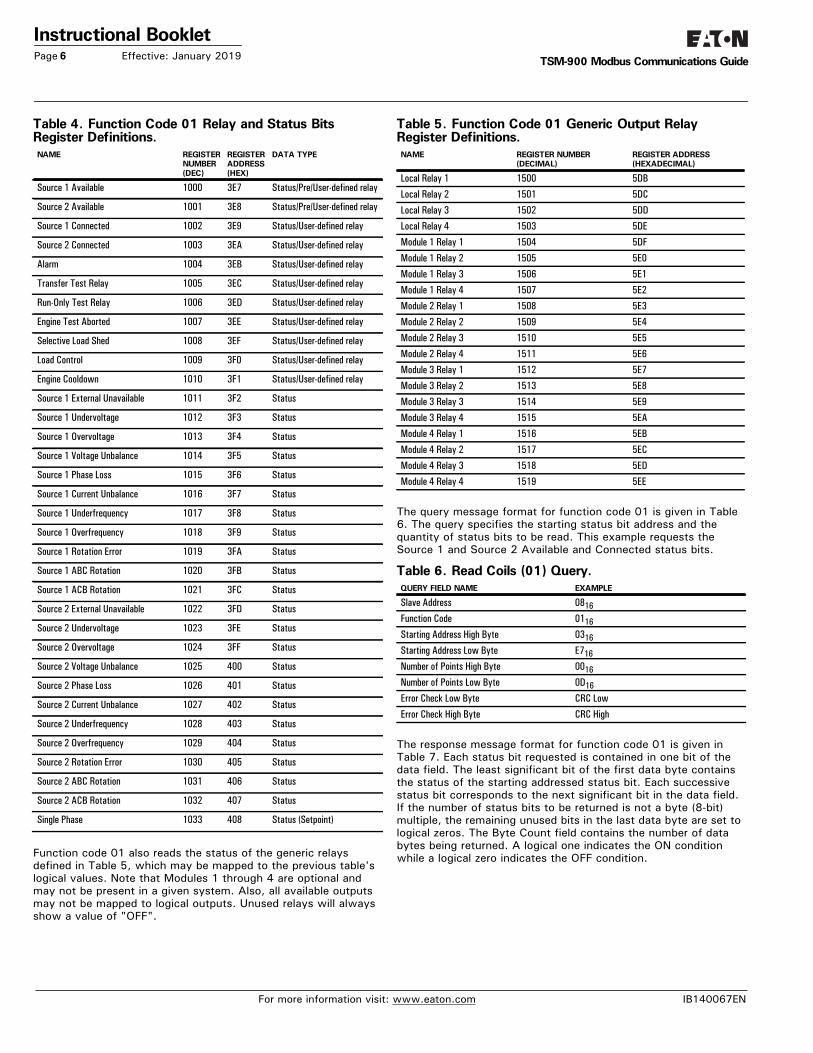
Table 4. Function Code 01 Relay and Status BitsRegister Definitions.
Function code 01 also reads the status of the generic relays defined in Table 5, which may be mapped to the previous table's logical values. Note that Modules 1 through 4 are optional and may not be present in a given system. Also, all available outputs may not be mapped to logical outputs. Unused relays will always show a value of "OFF".
Table 5. Function Code 01 Generic Output RelayRegister Definitions.
The query message format for function code 01 is given in Table 6. The query specifies the starting status bit address and the quantity of status bits to be read. This example requests the Source 1 and Source 2 Available and Connected status bits.
Table 6. Read Coils (01) Query.
The response message format for function code 01 is given in Table 7. Each status bit requested is contained in one bit of the data field. The least significant bit of the first data byte contains the status of the starting addressed status bit. Each successive status bit corresponds to the next significant bit in the data field. If the number of status bits to be returned is not a byte (8-bit) multiple, the remaining unused bits in the last data byte are set to logical zeros. The Byte Count field contains the number of data bytes being returned. A logical one indicates the ON condition while a logical zero indicates the OFF condition.
NAME REGISTER
NUMBER
(DEC)
REGISTER
ADDRESS
(HEX)
DATA TYPE
Source 1 Available 1000 3E7 Status/Pre/User-defined relay
Source 2 Available 1001 3E8 Status/Pre/User-defined relay
Source 1 Connected 1002 3E9 Status/User-defined relay
Source 2 Connected 1003 3EA Status/User-defined relay
Alarm 1004 3EB Status/User-defined relay
Transfer Test Relay 1005 3EC Status/User-defined relay
Run-Only Test Relay 1006 3ED Status/User-defined relay
Engine Test Aborted 1007 3EE Status/User-defined relay
Selective Load Shed 1008 3EF Status/User-defined relay
Load Control 1009 3F0 Status/User-defined relay
Engine Cooldown 1010 3F1 Status/User-defined relay
Source 1 External Unavailable 1011 3F2 Status
Source 1 Undervoltage 1012 3F3 Status
Source 1 Overvoltage 1013 3F4 Status
Source 1 Voltage Unbalance 1014 3F5 Status
Source 1 Phase Loss 1015 3F6 Status
Source 1 Current Unbalance 1016 3F7 Status
Source 1 Underfrequency 1017 3F8 Status
Source 1 Overfrequency 1018 3F9 Status
Source 1 Rotation Error 1019 3FA Status
Source 1 ABC Rotation 1020 3FB Status
Source 1 ACB Rotation 1021 3FC Status
Source 2 External Unavailable 1022 3FD Status
Source 2 Undervoltage 1023 3FE Status
Source 2 Overvoltage 1024 3FF Status
Source 2 Voltage Unbalance 1025 400 Status
Source 2 Phase Loss 1026 401 Status
Source 2 Current Unbalance 1027 402 Status
Source 2 Underfrequency 1028 403 Status
Source 2 Overfrequency 1029 404 Status
Source 2 Rotation Error 1030 405 Status
Source 2 ABC Rotation 1031 406 Status
Source 2 ACB Rotation 1032 407 Status
Single Phase 1033 408 Status (Setpoint)
NAME REGISTER NUMBER
(DECIMAL)
REGISTER ADDRESS
(HEXADECIMAL)
Local Relay 1 1500 5DB
Local Relay 2 1501 5DC
Local Relay 3 1502 5DD
Local Relay 4 1503 5DE
Module 1 Relay 1 1504 5DF
Module 1 Relay 2 1505 5E0
Module 1 Relay 3 1506 5E1
Module 1 Relay 4 1507 5E2
Module 2 Relay 1 1508 5E3
Module 2 Relay 2 1509 5E4
Module 2 Relay 3 1510 5E5
Module 2 Relay 4 1511 5E6
Module 3 Relay 1 1512 5E7
Module 3 Relay 2 1513 5E8
Module 3 Relay 3 1514 5E9
Module 3 Relay 4 1515 5EA
Module 4 Relay 1 1516 5EB
Module 4 Relay 2 1517 5EC
Module 4 Relay 3 1518 5ED
Module 4 Relay 4 1519 5EE
QUERY FIELD NAME EXAMPLE
Slave Address 0816Function Code 0116Starting Address High Byte 0316Starting Address Low Byte E716Number of Points High Byte 0016Number of Points Low Byte 0D16Error Check Low Byte CRC Low
Error Check High Byte CRC High
For more information visit: www.eaton.com IB140067EN

Instructional BookletEffective: January 2019 Page 7
TSM-900 Modbus Communications Guide
Table 7. Read Coils (01) Response.
3.2 Function Code 02 - Read Discrete Inputs
(Programmable Inputs Status)
Function code 02 reads the ON / OFF status of the programmable inputs in the TSM-900. "ON" means that the particular input fea-ture is active, regardless of the open/closed state of that input. "OFF" means that it is not active. For example, Lockout is ON/active when the associated input is Open, while Test Engine is ON/active when the associated input is Closed.Table 8 shows all of the possible programmable inputs available on the controller and accessory I/O modules. Typically, not all pro-grammable inputs are included in a given transfer switch imple-mentation. Unused inputs will always show a value of "OFF".
Table 8. Function Code 02 Programmable Input RegisterDefinitions.
Function code 2 also reads the status of the generic inputs defined in Table 9, which may be mapped to the previous table's logical values. A Logic 1 indicates that the input is Open while a logic 0 indicates that the input is closed. Note that Modules 1 through 4 are optional and may not be present in a given system. Also all available inputs may not be mapped to logical inputs. Any inputs not mapped to logical inputs will show the actual state of the input, while the inputs for modules which are not present will always show a value of "OFF".
Table 9. Function Code 02 Generic Input RegisterDefinitions.
The query message format for function code 02 is given in Table 10. The query specifies the starting address (which is always one less than the starting register number) and the quantity of binary inputs to be read.
Table 10. Read Input Status (02) Query.
The response message format for function code 02 is given in Table 11. Each binary input status requested is contained in one bit of the data field. The least significant bit of the first data byte contains the input status of the starting addressed input. Each successive input status bit corresponds to the next significant bit in the data field. If the number of inputs to be returned is not a byte (8-bit) multiple, the remaining unused bits in the last data byte are set to logical zeroes. The Byte Count field contains the number of data bytes being returned. A logical one indicates the ON condition while a logical zero indicates the OFF condition.
RESPONSE FIELD NAME EXAMPLE
Slave Address 0816Function Code 0116Byte Count 0216Data from Status Bits at X (e.g. 100010 through 100310) 0316Data from Status Bits at X+8 0116Error Check Low Byte CRC Low
Error Check High Byte CRC High
NAME
REGISTER NUMBER
(DECIMAL)
REGISTER ADDRESS
(HEXADECIMAL)
S1 Available 2000 7CF
S2 Available 2001 7D0
On Bypass 2002 7D1
Bypass Aux S1 Switch 2003 7D2
Bypass Aux S2 Switch 2004 7D3
Gen Start 2005 7D4
Door Open 2006 7D5
General Alarm 2007 7D6
ATS Not In Auto 2008 7D7
Lockout 2009 7D8
Manual Retransfer Enable 2010 7D9
Retransfer Request 2011 7DA
Go To Emergency 2012 7DB
Emergency Inhibit 2013 7DC
Go To Neutral 2014 7DD
Bypass Timers 2015 7DE
Engine Test 2016 7DF
Engine Test Mode 2017 7E0
Test Status 2018 7E1
NAME
REGISTER NUMBER
(DECIMAL) REGISTER ADDRESS (HEX)
Contact 1 2500 9C3
Contact 2 2501 9C4
Contact 3 2502 9C5
Contact 4 2503 9C6
Module 1 Contact 1 2504 9C7
Module 1 Contact 2 2505 9C8
Module 1 Contact 3 2506 9C9
Module 1 Contact 4 2507 9CA
Module 2 Contact 1 2508 9CB
Module 2 Contact 2 2509 9CC
Module 2 Contact 3 2510 9CD
Module 2 Contact 4 2511 9CE
Module 3 Contact 1 2512 9CF
Module 3 Contact 2 2513 9D0
Module 3 Contact 3 2514 9D1
Module 3 Contact 4 2515 9D2
Module 4 Contact 1 2516 9D3
Module 4 Contact 2 2517 9D4
Module 4 Contact 3 2518 9D5
Module 4 Contact 4 2519 9D6
QUERY FIELD NAME EXAMPLE
Slave Address 3416Function Code 0216Starting Address High Byte 0716Starting Address Low Byte D016Number of Points High Byte 0016Number of Points Low Byte 0316Error Check Low Byte CRC Low
Error Check High Byte CRC High
IB140067EN For more information visit: www.eaton.com

Instructional BookletPage 8 Effective: January 2019
TSM-900 Modbus Communications Guide
Table 11. Read Input Status (02) Response.
3.3 Function Code 03 - Read Holding Registers
(Setpoints)
Function code 03, Read Holding Registers, is used to read the set-points registers.Setpoints registers have been reserved to hold configuration infor-mation parameters that are programmable. Setpoints information starts at register number 3000 (i.e., holding register address BB716)
Setpoints Notes:
1. For various functional reasons in the controller, setpoints are broken up into six groups. The six groups of setpoints and their corresponding register numbers/addresses are defined in Table 12 through Table 17. This grouping has no effect on reading setpoints via Modbus.
2. Several setpoints are repeated as "Read Only" setpoints in various groups. This does not affect reading of these set-points, but does affect writing (Function codes 6 and 16).
3. Many setpoints are packed two to a register. These are shown in the following tables as two setpoints with the same register number/address and HOB or LOB. These are best understood in hexadecimal format where HOB indicates the upper eight bits and LOB indicates the lower eight bits of the 16-bit register. For example Group 0, register 8 is "Number of Generators and Number of Phases". A typical value for this register is 10316 meaning 1 generator and 3 phases. The reg-ister value in base 10 is 259.
To convert one of these dual setpoint registers from base 10, divide the register value by 256. The answer without the dec-imal is the HOB setpoint value. Multiply this answer by 256 and subtract it from the original register value to determine the LOB setpoint value t.
Again using the example above starting with a value of 259:
259 ÷ 256 = 1.0117, so the "Number of Generators" is 1
259 - (1 * 256) = 3, so the "Number of Phases" is 3
4. 4.The TSM-900 only supports fixed point values, thus the scale factor indicates what a decimal value has been multi-plied by prior to sending out via Modbus. For example, the various frequency values have a scale factor of 10. A typical reading may be 601, which is 60.1 Hz.
5. Setpoints are written using function code 6 or 16 (1016) as described in sections 3.6 and 3.8.
RESPONSE FIELD NAME EXAMPLE
Slave Address 3416Function Code 0216Byte Count 0116Data from Status Bits at X (e.g. 200010 through 200310) 0116Error Check Low Byte CRC Low
Error Check High Byte CRC High
For more information visit: www.eaton.com IB140067EN

Instructional BookletEffective: January 2019 Page 9
TSM-900 Modbus Communications Guide
Table 12. Function Code 03 Group 0 Setpoints Register Definitions.
Table 13. Function Code 03 Group 1 Setpoints Register Definitions.
Table 14. Function Code 03 Group 2 Setpoints Register Definitions.
.
NAME REGISTER NUMBER (DECIMAL) REGISTER ADDRESS (HEX) DATA RANGE SCALE FACTOR UNITS
Language 3000 HOB BB7 HOB 0 = English - -
Style (Read-Only) 3000 LOB BB7 LOB 1 = TSM-900 - -
CT Wiring Invert 3001 HOB BB8 HOB 0 = Normal, 1 = Invert - -
Sign Convention 3001 LOB BB8 LOB 0 = IEEE, 1 = IEEE Alternate - -
Line Frequency 3002 BB9 50 or 60 1 Hz
PT Ratio 3003 BBA 0 = None, 20 to 5000 10 -
CT Ratio 3004 BBB 0 = None, 100 to 5000 1 -
NTP Synchronization 3005 HOB BBC HOB 0 = Disabled, 1 = Enabled - -
Auto Clock DST Adjust 3005 LOB BBC LOB 0 = Disabled, 1 = Enabled - -
Time Zone Offset 3006 BBD -760 to + 840 - Mins.
System Voltage 3007 BBE 115 (50 Hz) or 120 (60 Hz) to 600 1 V
Sequence Check 3008 HOB BBF HOB 0 = Off, 1 = ABC, 2 = ACB - -
Number of Phases 3008 LOB BBF LOB 1 or 3 - -
Modbus Comm. Settings 3009 HOB BC0 HOB Baud Rate, Stop Bits, Parity0 = 9600 bps, 1, Even1 = 9600 bps, 1, Odd2 = 9600 bps, 2, None3 = 9600 bps, 1, None4 = 19200 bps, 1, Even5 = 19200 bps, 1, Odd6 = 19200 bps, 2, None7 = 19200 bps, 1, None8 = Disabled
- -
Modbus Address 3009 LOB BC0 LOB 1 - 247 - -
Name Register Number (decimal) Register Address (hex) Data Range Scale Factor Units
Line-to-Ground voltage display 3010 BC1 0 = Disabled, 1 = Enabled - -
Datalogging Interval 3011 BC2 1 to 120 - Mins
NAME REGISTER NUMBER (DECIMAL) REGISTER ADDRESS (HEX) DATA RANGE SCALE FACTOR UNITS
reserved for future use 3023 BCE See Setpoints Group 0 1 Sec.
Table 15. Function Code 03 Group 3 Setpoints Register Definitions
NAME REGISTER NUMBER (DEC) REGISTER ADDRESS (HEX) DATA RANGE
SCALE
FACTOR UNITS
System Voltage (Read-Only) 3012 BC3 See Setpoints Group 0 - -
System Frequency (Read-Only) 3013 BC4 See Setpoints Group 0 - -
Source 1 Undervoltage Dropout 3014 BC5 0 = disable,70% to 97% of System Voltage 1 V
Source 2 Undervoltage Dropout 3015 BC6 0 = disable,70% to 97% of System Voltage 1 V
Source 2 % UV Dropout (Read-Only) 3016 HOB BC7 HOB 0, 70 to 97 1 %
Source 1 % UV Dropout (Read-Only) 3016 LOB BC7 LOB 0, 70 to 97 1 %
Source 1 Undervoltage Pickup 3017 BC8 0 = disable, (dropout + 2%) to 99% of System Voltage 1 V
Source 2 Undervoltage Pickup 3018 BC9 0 = disable, (dropout + 2%) to 99% of System Voltage 1 V
IB140067EN For more information visit: www.eaton.com

Instructional BookletPage 10 Effective: January 2019
TSM-900 Modbus Communications Guide
Source 2 % UV Pickup (Read-Only) 3019 HOB BCA HOB 0, (dropout% + 2) to 99 1 %
Source 1 % UV Pickup (Read-Only) 3019 LOB BCA LOB 0, (dropout% + 2) to 99 1 %
Source 1 Overvoltage Dropout 3020 BCB 0 = disable, 105% to 120% of System Voltage 1 V
Source 2 Overvoltage Dropout 3021 BCC 0 = disable, 105% to 120% of System Voltage 1 V
Source 2 % OV Dropout (Read-Only) 3022 HOB BCD HOB 0, 105 to 120 1 %
Source 1 % OV Dropout (Read-Only) 3022 LOB BCD LOB 0, 105 to 120 1 %
Source 1 Overvoltage Pickup 3023 BCE 0 = disable, 103% to (dropout - 2%) of System Voltage 1 V
Source 2 Overvoltage Pickup 3024 BCF 0 = disable, 103% to (dropout - 2%) of System Voltage 1 V
Source 2 % OV Pickup (Read-Only) 3025 HOB BD0 HOB 0, 103 to (dropout% – 2) 1 %
Source 1 % OV Pickup (Read-Only) 3025 LOB BD0 LOB 0, 103 to (dropout% – 2) 1 %
Source 1 Underfrequency Dropout 3026 BD1 0 = Disable, 90% to 97% of Line Frequency 10 Hz
Source 2 Underfrequency Dropout 3027 BD2 0 = Disable, 90% to 97% of Line Frequency 10 Hz
Source 1 % Underfrequency Dropout (Read-Only) 3028 BD3 0, 90 to 97 1 %
Source 2 % Underfrequency Dropout (Read-Only) 3029 BD4 0, 90 to 97 1 %
Source 1 Underfrequency Pickup 3030 BD5 0 = Disable, (dropout + 10) to 99% of Line Frequency 10 Hz
Source 2 Underfrequency Pickup 3031 BD6 0 = Disable, (dropout + 10) to 99% of Line Frequency 10 Hz
Source 1 % Underfrequency Pickup (Read-Only) 3032 BD7 0 = Disable, (dropout% + 1) to 99 1 %
Source 2 % Underfrequency Pickup (Read-Only) 3033 BD8 0 = Disable, (dropout% + 1) to 99 1 %
Source 1 Overfrequency Dropout 3034 BD9 0 = Disable, 103% to 110% of Line Frequency 10 Hz
Source 2 Overfrequency Dropout 3035 BDA 0 = Disable, 103% to 110% of Line Frequency 10 Hz
Source 1 % Overfrequency Dropout (Read-Only) 3036 BDB 0, 103 to 110 1 %
Source 2 % Overfrequency Dropout (Read-Only) 3037 BDC 0, 103 to 110 1 %
Source 1 Overfrequency Pickup 3038 BDD 0 = Disable, 101% of Line Frequency to (dropout - 10) 10 Hz
Source 2 Overfrequency Pickup 3039 BDE 0 = Disable, 101% of Line Frequency to (dropout - 10) 10 Hz
Source 1 % Overfrequency Pickup (Read-Only) 3040 BDF 0, 101 to (dropout% - 1) 1 %
Source 2 % Overfrequency Pickup (Read-Only) 3041 BE0 0, 101 to (dropout% - 1) 1 %
Source 2 Voltage Unbalance Dropout % 3042 HOB BE1 HOB 0 = disable, 5 to 20 1 %
Source 1 Voltage Unbalance Dropout % 3042 LOB BE1 LOB 0 = disable, 5 to 20 1 %
Source 2 Voltage Unbalance Pickup % 3043 HOB BE2 HOB 0 = disable, 3 to (dropout - 2) 1 %
Source 1 Voltage Unbalance Pickup % 3043 LOB BE2 LOB 0 = disable, 3 to (dropout - 2) 1 %
Source 2 Voltage Phase Loss Dropout % 3044 HOB BE3 HOB 0 = disable, 20 to 60 1 %
Source 1 Voltage Phase Loss Dropout % 3044 LOB BE3 LOB 0 = disable, 20 to 60 1 %
Source 2 Voltage Phase Loss Pickup % 3045 HOB BE4 HOB 0 = disable, 18 to (dropout - 2) 1 %
Source 1 Voltage Phase Loss Pickup % 3045 LOB BE4 LOB 0 = disable, 18 to (dropout - 2) 1 %
Current Unbalance/Phase Loss Dropout % 3046 LOB BE5 LOB 0 = disable, 5 to 60 1 %
Current Unbalance/Phase Loss Enable % 3046 HOB BE5 HOB 1 to 100 (% of maximum load current) 1 %
Current Unbalance/Phase Loss Pickup % 3047 BE6 0 = disable, 3 to (dropout - 2) 1 %
Negative Sequence Time Delay 3048 BE7 10 to 30 1 Sec.
Table 15. Function Code 03 Group 3 Setpoints Register Definitions
NAME REGISTER NUMBER (DEC) REGISTER ADDRESS (HEX) DATA RANGE
SCALE
FACTOR UNITS
(Continued).
For more information visit: www.eaton.com IB140067EN

Instructional BookletEffective: January 2019 Page 11
TSM-900 Modbus Communications Guide
Table 16. Function Code 03 Group 4 Setpoints Register Definitions
NAME REGISTER NUMBER (DECIMAL) REGISTER ADDRESS (HEX) DATA RANGE
SCALE
FACTOR UNITS
Plant Exerciser 2 Test Mode 3049 HOB BE8 HOB 0 = Disabled1 = Run Unloaded,2 = Run Loaded
- -
Plant Exerciser 1 Test Mode 3049 LOB BE8 LOB 0 = Disabled1 = Run Unloaded,2 = Run Loaded
- -
Engine Test Mode 3050 BE9 0 = Disabled1 = Run Unloaded,2 = Run Loaded
- -
Engine Test Relays Config. 3051 BEA 0 = Transfer relay only for transfers1 = Both relays for transfers
- -
Plant Exerciser 1 Duration Timer 3052 BEB 0 to 600 1 Min.
Plant Exerciser 2 Duration Timer 3053 BEC 0 to 600 1 Min.
Engine Run Timer 3054 BED 0 to 600 1 Min.
Time Delay, Emergency Fail 3055 BEE 0 to 6 1 Sec.
Time Delay, Engine Cooldown 3056 BEF 0 to 9,999 1 Sec.
Time Delay, Normal to Emergency 3057 BF0 0 to 9,999 1 Sec.
Time Delay, Emergency to Normal 3058 BF1 0 to 9,999 1 Sec.
Plant Exerciser 1 Schedule Mode 3059 BF2 0=daily, 1=weekly, 2=14-day, 3=28-day, 4=dates
- -
Plant Exerciser 1 Month 1 3060 HOB BF3 HOB 1 = January to12 = December
- -
Plant Exerciser 1 Date 1 3060 LOB BF3 LOB 1 to 28, 30, or 31 (month dependent) - -
Plant Exerciser 1 Month 2 3061 HOB BF4 HOB 1 = January to12 = December
- -
Plant Exerciser 1 Date 2 3061 LOB BF4 LOB 1 to 28, 30, or 31 (month dependent) - -
Plant Exerciser 1 Month 3 3062 HOB BF5 HOB 1 = January to12 = December
- -
Plant Exerciser 1 Date 3 3062 LOB BF5 LOB 1 to 28, 30, or 31 (month dependent) - -
Plant Exerciser 1 Month 4 3063 HOB BF6 HOB 1 = January to12 = December
- -
Plant Exerciser 1 Date 4 3063 LOB BF6 LOB 1 to 28, 30, or 31 (month dependent) - -
Plant Exerciser 1 Month 5 3064 HOB BF7 HOB 1 = January to12 = December
- -
Plant Exerciser 1 Date 5 3064 LOB BF7 LOB 1 to 28, 30, or 31 (month dependent) - -
Plant Exerciser 1 Month 6 3065 HOB BF8 HOB 1 = January to12 = December
- -
Plant Exerciser 1 Date 6 3065 LOB BF8 LOB 1 to 28, 30, or 31 (month dependent) - -
Plant Exerciser 1 Month 7 3066 HOB BF9 HOB 1 = January to12 = December
- -
Plant Exerciser 1 Date 7 3066 LOB BF9 LOB 1 to 28, 30, or 31 (month dependent) - -
Plant Exerciser 1 Month 8 3067 HOB BFA HOB 1 = January to12 = December
- -
Plant Exerciser 1 Date 8 3067 LOB BFA LOB 1 to 28, 30, or 31 (month dependent) - -
Plant Exerciser 1 Month 9 3068 HOB BFB HOB 1 = January to12 = December
- -
Plant Exerciser 1 Date 9 3068 LOB BFB LOB 1 to 28, 30, or 31 (month dependent) - -
IB140067EN For more information visit: www.eaton.com

Instructional BookletPage 12 Effective: January 2019
TSM-900 Modbus Communications Guide
Plant Exerciser 1 Month 10 3069 HOB BFC HOB 1 = January to12 = December
- -
Plant Exerciser 1 Date 10 3069 LOB BFC LOB 1 to 28, 30, or 31 (month dependent) - -
Plant Exerciser 1 Month 11 3070 HOB BFD HOB 1 = January to12 = December
- -
Plant Exerciser 1 Date 11 3070 LOB BFD LOB 1 to 28, 30, or 31 (month dependent) - -
Plant Exerciser 1 Month 12 3071 HOB BFE HOB 1 = January to12 = December
- -
Plant Exerciser 1 Date 12 3071 LOB BFE LOB 1 to 28, 30, or 31 (month dependent) - -
Plant Exerciser 1 Hour 3072 HOB BFF HOB 0 to 23 - -
Plant Exerciser 1 Minute 3072 LOB BFF LOB 0 to 59 - -
Plant Exerciser 1 Day 3073 C00 1 = Sunday to 7 = Saturday - -
Plant Exerciser 2 Schedule Mode 3074 C01 0=daily, 1=weekly, 2=14-day, 3=28-day, 4=dates
- -
Plant Exerciser 2 Month 1 3075 HOB C02 HOB 1 = January to12 = December
- -
Plant Exerciser 2 Date 1 3075 LOB C02 LOB 1 to 28, 30, or 31 (month dependent) - -
Plant Exerciser 2 Month 2 3076 HOB C03 HOB 1 = January to12 = December
- -
Plant Exerciser 2 Date 2 3076 LOB C03 LOB 1 to 28, 30, or 31 (month dependent) - -
Plant Exerciser 2 Month 3 3077 HOB C04 HOB 1 = January to12 = December
- -
Plant Exerciser 2 Date 3 3077 LOB C04 LOB 1 to 28, 30, or 31 (month dependent) - -
Plant Exerciser 2 Month 4 3078 HOB C05 HOB 1 = January to12 = December
- -
Plant Exerciser 2 Date 4 3078 LOB C05 LOB 1 to 28, 30, or 31 (month dependent) - -
Plant Exerciser 2 Month 5 3079 HOB C06 HOB 1 = January to12 = December
- -
Plant Exerciser 2 Date 5 3079 LOB C06 LOB 1 to 28, 30, or 31 (month dependent) - -
Plant Exerciser 2 Month 6 3080 HOB C07 HOB 1 = January to12 = December
- -
Plant Exerciser 2 Date 6 3080 LOB C07 LOB 1 to 28, 30, or 31 (month dependent) - -
Plant Exerciser 2 Month 7 3081 HOB C08 HOB 1 = January to12 = December
- -
Plant Exerciser 2 Date 7 3081 LOB C08 LOB 1 to 28, 30, or 31 (month dependent) - -
Plant Exerciser 2 Month 8 3082 HOB C09 HOB 1 = January to12 = December
- -
Plant Exerciser 2 Date 8 3082 LOB C09 LOB 1 to 28, 30, or 31 (month dependent) - -
Plant Exerciser 2 Month 9 3083 HOB C0A HOB 1 = January to12 = December
- -
Plant Exerciser 2 Date 9 3083 LOB C0A LOB 1 to 28, 30, or 31 (month dependent) - -
Plant Exerciser 2 Month 10 3084 HOB C0B HOB 1 = January to12 = December
- -
Plant Exerciser 2 Date 10 3084 LOB C0B LOB 1 to 28, 30, or 31 (month dependent) - -
Plant Exerciser 2 Month 11 3085 HOB C0C HOB 1 = January to12 = December
- -
Plant Exerciser 2 Date 11 3085 LOB C0C LOB 1 to 28, 30, or 31 (month dependent) - -
Plant Exerciser 2 Month 12 3086 HOB C0D HOB 1 = January to12 = December
- -
Table 16. Function Code 03 Group 4 Setpoints Register Definitions
NAME REGISTER NUMBER (DECIMAL) REGISTER ADDRESS (HEX) DATA RANGE
SCALE
FACTOR UNITS
(Continued).
For more information visit: www.eaton.com IB140067EN

Instructional BookletEffective: January 2019 Page 13
TSM-900 Modbus Communications Guide
.
Plant Exerciser 2 Date 12 3086 LOB C0D LOB 1 to 28, 30, or 31 (month dependent) - -
Plant Exerciser 2 Hour 3087 HOB C0E HOB 0 to 23 - -
Plant Exerciser 2 Minute 3087 LOB C0E LOB 0 to 59 - -
Plant Exerciser 2 Day 3088 C0F 1 = Sunday to 7 = Saturday - -
Table 16. Function Code 03 Group 4 Setpoints Register Definitions
NAME REGISTER NUMBER (DECIMAL) REGISTER ADDRESS (HEX) DATA RANGE
SCALE
FACTOR UNITS
Table 17. Function Code 03 Group 5 Setpoints Register Definitions.
NAME
REGISTER NUMBER
(DECIMAL)
REGISTER ADDRESS
(HEX) DATA RANGE
SCALE
FACTOR UNITS
Number of Accessory I/O Modules 3089 HOB C10 HOB 0 to 4 - -
Style (Read-Only) 3089 LOB C10 LOB See Setpoints Group 0
Selective Load Shed Limit 3090 C11 5 to 3,000 1 KW
Local Programmable Inputs Factory Lock (Read-Only) 3091 C12 0 to 15 - -
Accessory I/O Module Programmable Inputs Factory Lock (Read-Only) 3092 C13 0 – 65,535 - -
Local Programmable Outputs Factory Lock (Read-Only) 3093 C14 0 to 15 - -
Accessory I/O Module Programmable Outputs Factory Lock (Read-Only) 3094 C15 0 – 65,535 - -
Selective Load Restore Limit 3095 C16 1 to(Selective Load Shed – 1)
1 KW
Local Input 1 Mapping 3096 C17 - -
Local Input 2 Mapping 3097 C18 - -
Local Input 3 Mapping 3098 C19 - -
Local Input 4 Mapping 3099 C1A - -
Local Output 2 Mapping 3100 HOB C1B HOB
Local Output 1 Mapping 3100 LOB C1B LOB - -
Local Output 4 Mapping 3101 HOB C1C HOB - -
Local Output 3 Mapping 3101 LOB C1C LOB - -
Module 1 Input 1 Mapping 3102 C1D - -
Module 1 Input 2 Mapping 3103 C1E - -
Module 1 Input 3 Mapping 3104 C1F - -
Module 1 Input 4 Mapping 3105 C20 - -
Module 1 Output 2 Mapping 3106 HOB C21 HOB - -
Module 1 Output 1 Mapping 3106 LOB C21 LOB - -
Module 1 Output 4 Mapping 3107 HOB C22 HOB - -
Module 1 Output 3 Mapping 3107 LOB C22 LOB - -
Module 2 Input 1 Mapping 3108 C23 - -
Module 2 Input 2 Mapping 3109 C24 - -
Module 2 Input 3 Mapping 3110 C25 - -
Module 2 Input 4 Mapping 3111 C26 - -
Module 2 Output 2 Mapping 3112 HOB C27 HOB - -
Module 2 Output 1 Mapping 3112 LOB C27 LOB - -
Module 2 Output 4 Mapping 3113 HOB C28 HOB - -
Module 2 Output 3 Mapping 3113 LOB C28 LOB - -
Module 3 Input 1 Mapping 3114 C29 - -
Module 3 Input 2 Mapping 3115 C2A - -
(Continued).
IB140067EN For more information visit: www.eaton.com

Instructional BookletPage 14 Effective: January 2019
TSM-900 Modbus Communications Guide
Table 18. Programmable Input Definitions. Table 19. Programmable Output Definitions.
Module 3 Input 3 Mapping 3116 C2B - -
Module 3 Input 4 Mapping 3117 C2C - -
Module 3 Output 2 Mapping 3118 HOB C2D HOB - -
Module 3 Output 1 Mapping 3118 LOB C2D LOB - -
Module 3 Output 4 Mapping 3119 HOB C2E HOB - -
Module 3 Output 3 Mapping 3119 LOB C2E LOB - -
Module 4 Input 1 Mapping 3120 C2F - -
Module 4 Input 2 Mapping 3121 C30 - -
Module 4 Input 3 Mapping 3122 C31 - -
Module 4 Input 4 Mapping 3123 C32 - -
Module 4 Output 2 Mapping 3124 HOB C33 HOB - -
Module 4 Output 1 Mapping 3124 LOB C33 LOB - -
Module 4 Output 4 Mapping 3125 HOB C34 HOB - -
Module 4 Output 3 Mapping 3125 LOB C34 LOB - -
Table 17. Function Code 03 Group 5 Setpoints Register Definitions.
NAME
REGISTER NUMBER
(DECIMAL)
REGISTER ADDRESS
(HEX) DATA RANGE
SCALE
FACTOR UNITS
VALUE DEFINITION
0 Disabled
1 S1 Available
2 S2 Available
3 Transfer Switch on Bypass
4 Bypass Aux S1 In
5 Bypass Aux S2 In
6 Gen Start Contact
7 Door Open
8 General Alarm
9 ATS Not In Automatic
10 Lockout
11 Enable Manual Retransfer
12 Manual Retransfer Request
13 Go To Emergency
14 Emergency Inhibit
15 Go To Neutral
16 Bypass Timers
17 Remote Engine Test
18 Engine Test Mode Select
19 Test Status
20 Remote I/O
VALUE DEFINITION
0 Disabled
1 Source 1 Available
2 Source 2 Available
3 Transfer Switch On Bypass
4 Source 1 Connected
5 Source 2 Connected
6 Gen Start
7 Door Open
8 Alarm
9 ATS Not In Automatic
10 Lockout
11 Enable Manual Retransfer
12 Manual Retransfer Request
13 Go To Emergency
14 Emergency Inhibit
15 Go To Neutral
16 ATS In Test
17 Transfer Test Contact Status
18 Run-Only Test Contact Status
19 Engine Test Aborted
20 Selective Load Shed
21 Load Bank Control
22 Cooldown In Progress
23 Remote I/O
(Continued).
For more information visit: www.eaton.com IB140067EN

Instructional BookletEffective: January 2019 Page 15
TSM-900 Modbus Communications Guide
Table 20. Write Setpoints Status and Multi-RegisterConfiguration Definitions.
The query message format for function code 03 is given in Table 21. The query specifies the starting register address (which is always one less than the starting register number) and the quan-tity of registers to be read.
Table 21. Read Setpoints Registers (03) Query.
The response message format for function code 03 is given in Table 22. The contents of each 16-bit register are returned as two bytes, with the high-order byte returned first. The Byte Count field contains the number of data bytes being returned, which is calculated as two times the number of registers requested.
Table 22. Read Setpoints Registers (03) Response.
3.4 Function Code 04 - Read Input Registers (Actual
Values)
Actual Value registers contain dynamic information such as device status and metered values, like voltages and frequencies (Table 23), fixed information such as firmware version numbers (Table 24), and historical information such as event data (Table 25) and high-speed capture data (Table 27). Actual value regis-ters are read-only and are accessed using function code 04.Table 23 provides a real-time view into various metered values, statistical information, and statuses.Note:
1. Most values are 16 bits (2 bytes) in length. However, the system counters are 32 bits (4 bytes) in length. These values are contained in two successive registers. The arrangement of the bytes in the 4-byte system counter values may be con-figured by setting the Multi-Register Configuration. See sec-tion 3.6.
2. The TSM-900 only supports fixed-point values, thus the scale factor indicates what a decimal value has been multiplied by prior to sending out via Modbus. For example, the various frequency values have a scale factor of 10. A typical reading may be 601, which is 60.1 Hz.
3. The time and data values are packed two bytes of data per register, indicated in the table with a colon ":" between val-ues.
4. TOC is Time of Change, and indicates the last time that a timer/counter was updated. TOR is Time of Reset and indi-cates the last time that a timer/counter was reset (via front panel display interface or Modbus command).
5. A * before a register address or number indicates a break in the normal sequential numbering, typically due to new regis-ters added after the product was released.
NAME
REGISTER
NUMBER
(DEC)
REGISTER
ADDRESS
(HEX) DATA RANGE
SCALE
FACTOR UNITS
Write Setpoints Status (Read-Only)
3126 C35 0 = No Error1-0xFFFF = Error while writing setpoints
- -
Multi-Register Configuration
3500 DAB 0 = High-Order Word in Lowest Register Number 1 - 0xFFFF = Low-Order Word in Lowest Register Number
- -
QUERY FIELD NAME EXAMPLE
Slave Address 2116Function Code 0316Starting Address High Byte 0B16Starting Address Low Byte B916Number of Registers High Byte 0016Number of Registers Low Byte 0216Error Check Low Byte CRC Low
Error Check High Byte CRC High
QUERY FIELD NAME EXAMPLE
Slave Address 2116Function Code 0316Byte Count 0416Data from High Byte of Regiser X (e.g., 0BB916) 0016Data from Low Byte of Regiser X (e.g., 0BB916) 0316Data from High Byte of Regiser X+1 (e.g., 0BBA16) 0016Data from Low Byte of Regiser X+1 (e.g., 0BBA16) 0516Error Check Low Byte CRC Low
Error Check High Byte CRC High
IB140067EN For more information visit: www.eaton.com

Instructional BookletPage 16 Effective: January 2019
TSM-900 Modbus Communications Guide
.
Table 23. Function Code 04 Actual Values (Dynamic Data) Register Definitions.
CATEGORY NAME UNITS
REGISTER NUMBER
(DEC)
REGISTER ADDRESS
(HEX)
SCALE
FACTOR FORMAT
Measured Values
Source 1 VAB V 6145 1800 1 Uint16
Source 1 VBC V 6146 1801 1 Uint16
Source 1 VCA V 6147 1802 1 Uint16
Source 1 VAG V 6148 1803 1 Uint16
Source 1 VBG V 6149 1804 1 Uint16
Source 1 VCG V 6150 1805 1 Uint16
Source 2 VAB V 6151 1806 1 Uint16
Source 2 VBC V 6152 1807 1 Uint16
Source 2 VCA V 6153 1808 1 Uint16
Source 2 VAG V 6154 1809 1 Uint16
Source 2 VBG V 6155 180A 1 Uint16
Source 2 VCG V 6156 180B 1 Uint16
Source 1/ Source 2 Max Voltage Difference V 6157 180C 1 Uint16
Load VAB V 6158 180D 1 Uint16
Load VBC V 6159 180E 1 Uint16
Load VCA V 6160 180F 1 Uint16
Load VAG V 6161 1810 1 Uint16
Load VBG V 6162 1811 1 Uint16
Load VCG V 6163 1812 1 Uint16
Source 1 Frequency Hz 6164 1813 10 Uint16
Source 2 Frequency Hz 6165 1814 10 Uint16
Source 1/ Source 2 Frequency Difference Hz 6166 1815 10 Uint16
Load Frequency Hz 6167 1816 10 Uint16
Load IA A 6168 1817 1 Uint16
Load IB A 6169 1818 1 Uint16
Load IC A 6170 1819 1 Uint16
Source 1 Voltage Unbalance % 6171 181A 10 Uint16
Source 2 Voltage Unbalance % 6172 181B 10 Uint16
Load Current Unbalance % 6173 181C 10 Uint16
Source 1/ Source 2 Phase Difference Deg 6174 181D 1 Uint16
Phase A Active Power high register W 6175 181E 1 Int32
Phase A Active Power low register W 6176 181F 1 Int32
Phase A Reactive Power high register VAR 6177 1820 1 Int32
Phase A Reactive Power low register VAR 6178 1821 1 Int32
Phase A Apparent Power high register VA 6179 1822 1 Uint32
Phase A Apparent Power low register VA 6180 1823 1 Uint32
Phase A Power Factor (Apparent) 6181 1824 100 Int16
Phase B Active Power high register W 6182 1825 1 Int32
Phase B Active Power low register W 6183 1826 1 Int32
Phase B Reactive Power high register VAR 6184 1827 1 Int32
Phase B Reactive Power low register VAR 6185 1828 1 Int32
Phase B Apparent Power high register VA 6186 1829 1 Uint32
(Continued).
For more information visit: www.eaton.com IB140067EN

Instructional BookletEffective: January 2019 Page 17
TSM-900 Modbus Communications Guide
Phase B Apparent Power low register VA 6187 182A 1 Uint32
Phase B Power Factor (Apparent) 6188 182B 100 Int16
Phase C Active Power high register W 6189 182C 1 Int32
Phase C Active Power low register W 6190 182D 1 Int32
Phase C Reactive Power high register VAR 6191 182E 1 Int32
Phase C Reactive Power low register VAR 6192 182F 1 Int32
Phase C Apparent Power high register VA 6193 1830 1 Uint32
Phase C Apparent Power low register VA 6194 1831 1 Uint32
Phase C Power Factor (Apparent) 6195 1832 100 Int16
Total Active Power high register W 6196 1833 1 Int32
Total Active Power low register W 6197 1834 1 Int32
Total Reactive Power high register VAR 6198 1835 1 Int32
Total Reactive Power low register VAR 6199 1836 1 Int32
Total Apparent Power high register VA 6200 1837 1 Uint32
Total Apparent Power low register VA 6201 1838 1 Uint32
Power Factor (Apparent) 6202 1839 100 Int16
Timers
TDEC Timer seconds 6203 183A 1 Uint16
TDEF Timer seconds 6204 183B 1 Uint16
Engine Run Timer seconds 6205 183C 1 Uint16
S1 Negative Sequence Timer seconds 6206 183D 1 Uint16
S1 Negative Sequence Timer seconds 6207 183E 1 Uint16
System Counters
Transfer Time(valid when connected to Source 2, else zero)
seconds 6208 183F 100 Uint16
Transfer Time(always returns last transfer time)
seconds 6355 18D2 100 Uint16
Transfer Time TOC month : date 1-12 : 1-31 6209 1840 - Uint16
Transfer Time TOC year : day 0-99 : 1-7 6210 1841 - Uint16
Transfer Time TOC hour : minute 0-23 : 0-59 6211 1842 - Uint16
Transfer Time TOC second : 1/100 second 0-59 : 0-99 6212 1843 - Uint16
Transfer Test Time high register minutes 6213 1844 - Uint16
Transfer Test Time low register minutes 6214 1845 - Uint16
Transfer Test TOC month : date 1-12 : 1-31 6215 1846 - Uint16
Transfer Test TOC year : day 0-99 : 1-7 6216 1847 - Uint16
Transfer Test TOC hour : minute 0-23 : 0-59 6217 1848 - Uint16
Transfer Test TOC second : 1/100 second 0-59 : 0-99 6218 1849 - Uint16
Transfer Test TOR month : date 1-12 : 1-31 6219 184A - Uint16
Transfer Test TOR year : day 0-99 : 1-7 6220 184B - Uint16
Transfer Test TOR hour : minute 0-23 : 0-59 6221 184C - Uint16
Transfer Test TOR second : 1/100 second 0-59 : 0-99 6222 184D - Uint16
Run-Only Test Time high register minutes 6223 184E - Uint16
Run-Only Test Time low register minutes 6224 184F - Uint16
Run-Only Test TOC month : date 1-12 : 1-31 6225 1850 - Uint16
Run-Only Test TOC year : day 0-99 : 1-7 6226 1851 - Uint16
Table 23. Function Code 04 Actual Values (Dynamic Data) Register Definitions.
CATEGORY NAME UNITS
REGISTER NUMBER
(DEC)
REGISTER ADDRESS
(HEX)
SCALE
FACTOR FORMAT
(Continued).
IB140067EN For more information visit: www.eaton.com

Instructional BookletPage 18 Effective: January 2019
TSM-900 Modbus Communications Guide
Run-Only Test TOC hour : minute 0-23 : 0-59 6227 1852 - Uint16
Run-Only Test TOC second : 1/100 second 0-59 : 0-99 6228 1853 - Uint16
Run-Only Test TOR month : date 1-12 : 1-31 6229 1854 - Uint16
Run-Only Test TOR year : day 0-99 : 1-7 6230 1855 - Uint16
Run-Only Test TOR hour : minute 0-23 : 0-59 6231 1856 - Uint16
Run-Only Test TOR second : 1/100 second 0-59 : 0-99 6232 1857 - Uint16
S1 Available Time high register minutes 6233 1858 - Uint16
S1 Available Time low register minutes 6234 1859 - Uint16
S1 Available TOC month : date 1-12 : 1-31 6235 185A - Uint16
S1 Available TOC year : day 0-99 : 1-7 6236 185B - Uint16
S1 Available TOC hour : minute 0-23 : 0-59 6237 185C - Uint16
S1 Available TOC second : 1/100 second 0-59 : 0-99 6238 185D - Uint16
S1 Available TOR month : date 1-12 : 1-31 6239 185E - Uint16
S1 Available TOR year : day 0-99 : 1-7 6240 185F - Uint16
S1 Available TOR hour : minute 0-23 : 0-59 6241 1860 - Uint16
S1 Available TOR second : 1/100 second 0-59 : 0-99 6242 1861 - Uint16
S2 Available Time high register minutes 6243 1862 - Uint16
S2 Available Time low register minutes 6244 1863 - Uint16
S2 Available TOC month : date 1-12 : 1-31 6245 1864 - Uint16
S2 Available TOC year : day 0-99 : 1-7 6246 1865 - Uint16
S2 Available TOC hour : minute 0-23 : 0-59 6247 1866 - Uint16
S2 Available TOC second : 1/100 second 0-59 : 0-99 6248 1867 - Uint16
S2 Available TOR month : date 1-12 : 1-31 6249 1868 - Uint16
S2 Available TOR year : day 0-99 : 1-7 6250 1869 - Uint16
S2 Available TOR hour : minute 0-23 : 0-59 6251 186A - Uint16
S2 Available TOR second : 1/100 second 0-59 : 0-99 6252 186B - Uint16
S1 Connect Time high register minutes 6253 186C - Uint16
S1 Connect Time low register minutes 6254 186D - Uint16
S1 Connect TOC month : date 1-12 : 1-31 6255 186E - Uint16
S1 Connect TOC year : day 0-99 : 1-7 6256 186F - Uint16
S1 Connect TOC hour : minute 0-23 : 0-59 6257 1870 - Uint16
S1 Connect TOC second : 1/100 second 0-59 : 0-99 6258 1871 - Uint16
S1 Connect TOR month : date 1-12 : 1-31 6259 1872 - Uint16
S1 Connect TOR year : day 0-99 : 1-7 6260 1873 - Uint16
S1 Connect TOR hour : minute 0-23 : 0-59 6261 1874 - Uint16
S1 Connect TOR second : 1/100 second 0-59 : 0-99 6262 1875 - Uint16
S2 Connect Time high register minutes 6263 1876 - Uint16
S2 Connect Time low register minutes 6264 1877 - Uint16
S2 Connect TOC month : date 1-12 : 1-31 6265 1878 - Uint16
S2 Connect TOC year : day 0-99 : 1-7 6266 1879 - Uint16
S2 Connect TOC hour : minute 0-23 : 0-59 6267 187A - Uint16
S2 Connect TOC second : 1/100 second 0-59 : 0-99 6268 187B - Uint16
Table 23. Function Code 04 Actual Values (Dynamic Data) Register Definitions.
CATEGORY NAME UNITS
REGISTER NUMBER
(DEC)
REGISTER ADDRESS
(HEX)
SCALE
FACTOR FORMAT
(Continued).
For more information visit: www.eaton.com IB140067EN

Instructional BookletEffective: January 2019 Page 19
TSM-900 Modbus Communications Guide
S2 Connect TOR month : date 1-12 : 1-31 6269 187C - Uint16
S2 Connect TOR year : day 0-99 : 1-7 6270 187D - Uint16
S2 Connect TOR hour : minute 0-23 : 0-59 6271 187E - Uint16
S2 Connect TOR second : 1/100 second 0-59 : 0-99 6272 187F - Uint16
Load EnergizedTime high register minutes 6273 1880 - Uint16
Load Energized Time low register minutes 6274 1881 - Uint16
Load Energized TOC month : date 1-12 : 1-31 6275 1882 - Uint16
Load Energized TOC year : day 0-99 : 1-7 6276 1883 - Uint16
Load Energized TOC hour : minute 0-23 : 0-59 6277 1884 - Uint16
Load Energized TOC second : 1/100 second 0-59 : 0-99 6278 1885 - Uint16
Load Energized TOR month : date 1-12 : 1-31 6279 1886 - Uint16
Load Energized TOR year : day 0-99 : 1-7 6280 1887 - Uint16
Load Energized TOR hour : minute 0-23 : 0-59 6281 1888 - Uint16
Load Energized TOR second : 1/100 second 0-59 : 0-99 6282 1889 - Uint16
Tier 4 Time high register minutes 6283 188A - Uint16
Tier 4 Time low register minutes 6284 188B - Uint16
Tier 4 TOC month : date 1-12 : 1-31 6285 188C - Uint16
Tier 4 TOC year : day 0-99 : 1-7 6286 188D - Uint16
Tier 4 TOC hour : minute 0-23 : 0-59 6287 188E - Uint16
Tier 4 TOC second : 1/100 second 0-59 : 0-99 6288 188F - Uint16
Tier 4 TOR month : date 1-12 : 1-31 6289 1890 - Uint16
Tier 4 TOR year : day 0-99 : 1-7 6290 1891 - Uint16
Tier 4 TOR hour : minute 0-23 : 0-59 6291 1892 - Uint16
Tier 4 TOR second : 1/100 second 0-59 : 0-99 6292 1893 - Uint16
Number of Transfers 6293 1894 - Uint16
Number of Transfers TOC month : date 1-12 : 1-31 6294 1895 - Uint16
Number of Transfers TOC year : day 0-99 : 1-7 6295 1896 - Uint16
Number of Transfers TOC hour : minute 0-23 : 0-59 6296 1897 - Uint16
Number of Transfers TOC sec:1/100 sec 0-59 : 0-99 6297 1898 - Uint16
Number of Transfers TOR month : date 1-12 : 1-31 6298 1899 - Uint16
Number of Transfers TOR year : day 0-99 : 1-7 6299 189A - Uint16
Number of Transfers TOR hour : minute 0-23 : 0-59 6300 189B 1 Uint16
Number of Transfers TOR sec:1/100 sec 0-59 : 0-99 6301 189C - Uint16
Number of Transfer Tests 6302 189D - Uint16
Number of Transfer Tests TOC month : date 1-12 : 1-31 6303 189E - Uint16
Number of Transfer Tests TOC year : day 0-99 : 1-7 6304 189F - Uint16
Number of Transfer Tests TOC hour : minute 0-23 : 0-59 6305 18A0 - Uint16
Number of Transfer Tests TOC sec:1/100 sec 0-59 : 0-99 6306 18A1 - Uint16
Number of Transfer Tests TOR month : date 1-12 : 1-31 6307 18A2 - Uint16
Number of Transfer Tests TOR year : day 0-99 : 1-7 6308 18A3 - Uint16
Number of Transfer Tests TOR hour : minute 0-23 : 0-59 6309 18A4 1 Uint16
Number of Transfer Tests TOR sec:1/100 sec 0-59 : 0-99 6310 18A5 - Uint16
Table 23. Function Code 04 Actual Values (Dynamic Data) Register Definitions.
CATEGORY NAME UNITS
REGISTER NUMBER
(DEC)
REGISTER ADDRESS
(HEX)
SCALE
FACTOR FORMAT
(Continued).
IB140067EN For more information visit: www.eaton.com

Instructional BookletPage 20 Effective: January 2019
TSM-900 Modbus Communications Guide
Table 24. Decoding for Primary Status Register.
Table 25. Decoding for Secondary Status Register.
Table 26. Decoding for Cause of Status Register.
Number of Run-Only Tests 6311 18A6 - Uint16
Number of Run-Only Tests TOC month : date 1-12 : 1-31 6312 18A7 - Uint16
Number of Run-Only Tests TOC year : day 0-99 : 1-7 6313 18A8 - Uint16
Number of Run-Only Tests TOC hour : minute 0-23 : 0-59 6314 18A9 - Uint16
Number of Run-Only Tests TOC sec:1/100 sec 0-59 : 0-99 6315 18AA - Uint16
Number of Run-Only Tests TOR month : date 1-12 : 1-31 6316 18AB - Uint16
Number of Run-Only Tests TOR year : day 0-99 : 1-7 6317 18AC - Uint16
Number of Run-Only Tests TOR hour : minute 0-23 : 0-59 6318 18AD 1 Uint16
Number of Run-Only Tests TOR sec:1/100 sec 0-59 : 0-99 6319 18AE - Uint16
Transfer Switch Status Information
Primary Status Table 24 6320 18AF 1 Uint16
Secondary Status Table 25 6321 18B0 1 Uint16
Cause of Status Table 26 6322 18B1 - Uint16
Source 1 Status Table 27 6323 18B2 - Uint16
Source 2 Status Table 27 6324 18B3 - Uint16
Binary Status Bits Table 28 6325 18B4 - Uint16
Binary Status2 Bits Table 29 6326 18B5 - Uint16
Alarm Status Bits Table 30 6327 18B6 - Uint16
Table 23. Function Code 04 Actual Values (Dynamic Data) Register Definitions.
CATEGORY NAME UNITS
REGISTER NUMBER
(DEC)
REGISTER ADDRESS
(HEX)
SCALE
FACTOR FORMAT
CODE DEFINITION
4 Alarmed
8 Starting
9 Operational
11 Locked-Out
12 Transferred
27 On Good Source
CODE DEFINITION
1 Not Applicable
3 Test Mode
7 Powered Up Since Last Alarm Reset
CODE DEFINITION
0 Unknown
1 Normal Operating Mode
11 Overvoltage
12 Undervoltage
15 Underfrequency
16 Overfrequency
17 Current Unbalance
18 Voltage Unbalance
39 Diagnostic Warning #1 (A/D Calibration)
68 Reverse Sequence
71 Alarm Active
74 Lockout
77 Setpoints Error
113 Calibration
132 Plant Exercise
136 Real Time Clock
153 Monitor Mode (ATS Not in Automatic)
2043 Phase Loss
2044 RAM Error
2045 Non-volatile Memory Error
2046 Watchdog
2047 ROM Error
(Continued).
For more information visit: www.eaton.com IB140067EN

Instructional BookletEffective: January 2019 Page 21
TSM-900 Modbus Communications Guide
Table 27. Decoding for Source 1 / Source 2 StatusRegisters.
Table 28. Decoding for Binary Status Register.
Table 29. Decoding for Binary Status Register 2.
Table 30. Decoding for Alarm Status Register.
Table 31 contains fixed data which typically does not change.
Note:
1. The ASCII strings are packed two characters per register, with the HOB in the lowest numbered register containing the leftmost character in the string, going to the LOB in the high-est numbered register containing the rightmost character in the string. Unused characters are NULL (0x00) and padded on the right side of the string.
2. The Display and Gen Start firmware/revision numbers will be zero for up to 70 seconds after power-on.
Table 31. Function Code 04 Actual Values (Fixed Data) Register Definitions
Table 32 contains historical event log entries. Each entry is the latest occurrence for that type of event.Note:
1. Most values are 16 bits (2 bytes) in length. However, the Event IDs are 32 bits (4 bytes) in length. These values are contained in two successive registers. The arrangement of the bytes in the 4-byte system counter values may be config-ured by writing the Multi-Register Configuration. See section 3.6.
2. The Event ID is a sequential number generated by the control-ler at the time of an event. It can be useful for sorting or if the timestamp is ambiguous, such as if events occur during both the hour before and the hour after switching back from day-light savings time to standard time.
3. Although Table 33 shows all of the "Event Codes", each event type only uses a subset of the codes.
4. The various Input and Output events coincide with all possi-ble programmable input and output types. Only those that are actually used will be updated.
5. The S1/S2 Unavailable Events and the Transfer Step events contain a snapshot of various voltages/currents and statuses at the time that the event occurred.
CODE DEFINITION
0 Normal
1 Undervoltage
2 Overvoltage
3 Underfrequency
4 Overfrequency
5 Voltage Unbalance
6 Phase Reversal
7 Phase Loss
8 Current Unbalance
9 External Available Input
CODE DEFINITION
0 Source 1 Connected
1 Source 2 Connected
2 ATS Transferred
3 Alarm
4 Source 1 Available
5 Source 2 Available
6 Rotation ACB
7 Waiting for Transfer
8 Engine Transfer Test
9 Engine Run-only Test
10 Transfer Switch in Test
11 Transfer in Progress
12 Single Phase
13 Transfer Switch in Bypass
14 Source 1 Available External Input
15 Source 2 Available External Input
CODE DEFINITION
0 DCT Module Detected
1 ATS Not in Automatic
2 Go to Emergency
3 Emergency Inhibit
4 Go to Neutral
5 - 15 Reserved for internal use
CODE DEFINITION
0 Lockout
1 Engine Test Aborted
2 Generator Unavailable
3 External Alarm
4 Door Alarm
5 - 14 Reserved for Future Use
15 Infernal Controller Electronic Fault
CATEGORY NAME UNITS
REGISTER
NUMBER
(DEC)
REGISTER
ADDRESS
(HEX)
SCALE
FACTOR FORMAT
Controller Info
Product ID (TSM-900) – start
- 6228 18B7 - ASCII
… - … … - ASCII
Product ID – end - 6331 18BA - ASCII
Hardware Revision - 6332 18BB - Uint16
DSP Firmware Version : Revision
- 6333 18BC - Uint16
Display Firmware Ver-sion : Revision
- 6334 18BD - Uint16
Gen Start Firmware Version : Revision
- 6335 18BD - Uint16
Serial Number – start - 6336 18BF - ASCII
…(8) - … … - ASCII
Serial Number – end - 6345 18B8 - ASCII
Date Code – start - 6346 18C9 - ASCII
…(2) - … … - ASCII
Date Code – end - 6249 18CC - ASCII
GO Number – start - 6250 18CD - ASCII
…(3) - … … - ASCII
GO Number – end - 6354 18D1 - ASCII
IB140067EN For more information visit: www.eaton.com

Instructional BookletPage 22 Effective: January 2019
TSM-900 Modbus Communications Guide
Table 32. Function Code 04 Actual Values (Event Data) Register Definitions (Continued).CATEGORY NAME UNITS OR VALUE LIMITS REGISTER NUMBER (DEC) REGISTER ADDRESS (HEX) SCALE FACTOR FORMAT
Power-Up Event
Event ID low register - 7000 1B57 - Uint32
Event ID high register - 7001 1B58 - Uint32
Event Timestamp month : date 1-12 : 1-31 7002 1B59 - Uint16
Event Timestamp year : day 0-99 : 1-7 7003 1B5A - Uint16
Event Timestamp hour : minute 0-23 : 0-59 7004 1B5B - Uint16
Event Timestamp second : 1/100 second 0-59 : 0-99 7005 1B5C - Uint16
Event Code Table33 7006 1B5D - Uint16
Setpoint Download Same format as Power-Up Event - 7007 1B5E - -
Counter/Timer Reset
Same format as Power-Up Event - 7014 1B65 - -
Bypass Timer Same format as Power-Up Event - 7021 1B6C - -
Internal Alarm Same format as Power-Up Event - 7028 1B73 - -
Reset Alarm Same format as Power-Up Event - 7035 1B7A - -
Plant Exercise Same format as Power-Up Event - 7042 1B81 - -
Transfer Test Relay Same format as Power-Up Event - 7049 1B88 - -
Run-Only Test Relay Same format as Power-Up Event - 7056 1B8F - -
S1 Avail. Input Same format as Power-Up Event - 7063 1B96 - -
S2 Avail. Input Same format as Power-Up Event - 7070 1B9D - -
On Bypass Input Same format as Power-Up Event - 7077 1BA4 - -
Bypass S1 Aux. Input Same format as Power-Up Event - 7084 1BAB - -
Bypass S2 Aux. Input Same format as Power-Up Event - 7091 1BB2 - -
Generator Start Input Same format as Power-Up Event - 7098 1BB9 - -
Door Open Input Same format as Power-Up Event - 7105 1BC0 - -
General Alarm Input Same format as Power-Up Event - 7112 1BC7 - -
ATS Not In Auto. Input Same format as Power-Up Event - 7119 1BCE - -
Lockout Input Same format as Power-Up Event - 7126 1BD5 - -
Manual Retransfer Enable Input
Same format as Power-Up Event - 7133 1BDC - -
Manual Retransfer Request Input
Same format as Power-Up Event - 7140 1BE3 - -
Go To Emergency Input Same format as Power-Up Event - 7147 1BEA - -
Emergency Inhibit Input
Same format as Power-Up Event - 7154 1BF1 - -
Go To Neutral Input Same format as Power-Up Event - 7161 1BF8 - -
Bypass Timers Input Same format as Power-Up Event - 7168 1BFF - -
Engine Test Input Same format as Power-Up Event - 7175 1C06 - -
Engine Test Mode Input Same format as Power-Up Event - 7182 1C0D - -
Test Status Input Same format as Power-Up Event - 7189 1C14 - -
S1 Avail. Output Same format as Power-Up Event - 7196 1C1B - -
S2 Avail. Output Same format as Power-Up Event - 7203 1C22 - -
Transfer Switch On Bypess Output
Same format as Power-Up Event - 7210 1C29 - -
S1 Conn. Output Same format as Power-Up Event - 7217 1C30 - -
S2 Conn. Output Same format as Power-Up Event - 7224 1C37 - -
Gen Start Output Same format as Power-Up Event - 7231 1C3E - -
Door Open Output Same format as Power-Up Event - 7238 1C45 - -
For more information visit: www.eaton.com IB140067EN

Instructional BookletEffective: January 2019 Page 23
TSM-900 Modbus Communications Guide
Alarm Output Same format as Power-Up Event - 7245 1C4C - -
ATS Not In Automatic Output
Same format as Power-Up Event - 7252 1C53 - -
Lockout Output Same format as Power-Up Event - 7259 1C5A - -
Manual Retransfer Enable Output
Same format as Power-Up Event - 7266 1C61 - -
Manual Retransfer Request Output
Same format as Power-Up Event - 7273 1C68 - -
Go To Emergency Out-put
Same format as Power-Up Event - 7280 1C6F - -
Emergency Inhibit Out-put
Same format as Power-Up Event - 7287 1C76 - -
Go To Neutral Output Same format as Power-Up Event - 7294 1C7D - -
ATS In Test Output Same format as Power-Up Event - 7301 1C84 - -
Transfer Test Contact Status Output
Same format as Power-Up Event - 7308 1C8B - -
Run-Only Test Contact Status Output
Same format as Power-Up Event - 7315 1C92 - -
Engine Test Aborted Output
Same format as Power-Up Event - 7322 1C99 - -
Selective Load Shed Output
Same format as Power-Up Event - 7329 1CA0 - -
Load Bank Control Out-put
Same format as Power-Up Event - 7336 1CA7 - -
Cooldown In Progress Output
Same format as Power-Up Event - 7343 1CAE - -
Time Adjustment Event
Event ID low register - 7350 1CB5 - -
Event ID high register - 7351 1CB6 - Uint32
Old Time month : date 1-12 : 1-31 7352 1CB7 - Uint16
Old Time year : day 0-99 : 1-7 7353 1CB8 - Uint16
Old Time hour : minute 0-23 : 0-59 7354 1CB9 - Uint16
Old Time second : 1/100 second 0-59 : 0-99 7355 1CBA - Uint16
Event Code 7356 1CBB - Uint16
New Time month : date 1-12 : 1-31 7357 1CBC - Uint16
New Time year : day 0-99 : 1-7 7358 1CBD - Uint16
New Time hour : minute 0-23 : 0-59 7359 1CBE - Uint16
New Time second : 1/100 second 0-59 : 0-99 7360 1CBF - Uint16
Table 32. Function Code 04 Actual Values (Event Data) Register Definitions (Continued).CATEGORY NAME UNITS OR VALUE LIMITS REGISTER NUMBER (DEC) REGISTER ADDRESS (HEX) SCALE FACTOR FORMAT
IB140067EN For more information visit: www.eaton.com

Instructional BookletPage 24 Effective: January 2019
TSM-900 Modbus Communications Guide
Source 1 Unavailable Event
Event ID low register - 7361 1CC0 - Uint32
Event ID high register - 7362 1CC1 - Uint32
Event Time Stamp month : date 1-12 : 1-31 7363 1CC2 - Uint16
Event Time Stamp year : day 0-99 : 1-7 7364 1CC3 - Uint16
Event Time Stamp hour : minute 0-23 : 0-59 7365 1CC4 - Uint16
Event Time Stamp second : 1/100 second 0-59 : 0-99 7366 1CC5 - Uint16
Validity bits low register - 7367 1CC6 - Uint16
Validity bits high register - 7368 1CC7 - Uint16
Event Code : Cause of Alarm Code 0 : 7369 1CC8 - Uint16
Source 1 VAB V 7370 1CC9 1 Uint16
Source 1 VBC V 7371 1CCA 1 Uint16
Source 1 VCA V 7372 1CCB 1 Uint16
Source 2 VAB V 7373 1CCC 1 Uint16
Source 2 VBC V 7374 1CCD 1 Uint16
Source 2 VCA V 7375 1CCE 1 Uint16
Load VAB V 7376 1CCF 1 Uint16
Load VBC V 7377 1CD0 1 Uint16
Load VCA V 7378 1CD1 1 Uint16
Load IA A 7379 1CD2 1 Uint16
Load IB A 7380 1CD3 1 Uint16
Load IC A 7381 1CD4 1 Uint16
Source 1 Frequency Hz 7382 1CD5 10 Uint16
Source 2 Frequency Hz 7381 1CD4 10 Uint16
Load Frequency Hz 7382 1CD5 10 Uint16
Source 1 Status : Source 2 Status : 7383 1CD6 - Uint16
Binary Status Bits 7384 1CD7 - Uint16
Binary Status Validity Mask 0xFFFF 7385 1CD8 - Uint16
S2 Unavailable Event Same format as Source 1 Unavailable Event
7386 1CD9 - -
Table 32. Function Code 04 Actual Values (Event Data) Register Definitions (Continued).CATEGORY NAME UNITS OR VALUE LIMITS REGISTER NUMBER (DEC) REGISTER ADDRESS (HEX) SCALE FACTOR FORMAT
For more information visit: www.eaton.com IB140067EN

Instructional BookletEffective: January 2019 Page 25
TSM-900 Modbus Communications Guide
Transfer Connected to Source 1 Event
Event ID low register - 7387 1CDA - Uint32
Event ID high register - 7388 1CDB - Uint32
Event Time Stamp month : date 1-12 : 1-31 7389 1CDC - Uint16
Event Time Stamp year : day 0-99 : 1-7 7390 1CDD - Uint16
Event Time Stamp hour : minute 0-23 : 0-59 7391 1CDE - Uint16
Event Time Stamp second : 1/100 second 0-59 : 0-99 7392 1CDF - Uint16
Validity bits low register - 7393 1CE0 - Uint16
Validity bits high register - 7394 1CE1 - Uint16
Event Code 7395 1CE2 - Uint16
Source 1 VAB V 7396 1CE3 1 Uint16
Source 1 VBC V 7397 1CE4 1 Uint16
Source 1 VCA V 7398 1CE5 1 Uint16
Source 2 VAB V 7399 1CE6 1 Uint16
Source 2 VBC V 7400 1CE7 1 Uint16
Source 2 VCA V 7401 1CE8 1 Uint16
Load VAB V 7402 1CE9 1 Uint16
Load VBC V 7403 1CEA 1 Uint16
Load VCA V 7404 1CEB 1 Uint16
Load IA A 7405 1CEC 1 Uint16
Load IB A 7406 1CED 1 Uint16
Load IC A 7407 1CEE 1 Uint16
Source 1 Frequency Hz 7408 1CEF 10 Uint16
Source 2 Frequency Hz 7409 1CF0 10 Uint16
Load Frequency Hz 7410 1CF1 10 Uint16
Source 1 Status : Source 2 Status : 7411 1CF2 - Uint16
Binary Status Bits 7441 1D10 - Uint16
Binary Status Validity Mask 0xFFFF 7471 1D2E - Uint16
Transfer ID - 7501 1D4C - Uint16
Next Sample : Post Transfer Counter 0-199 : 0-100 7502 1D4D - Uint16
Spare - 7503 1D4E - Uint16
Transfer To Neutral Event
Same format as Transfer Connected to Source 1 Event
- 7504 1D4F - -
Transfer To Parallel Event
Same format as Transfer Connected to Source 1 Event
- 7505 1D50 - -
Transfer Connected to Source 2 Event
Same format as Transfer Connected to Source 1 Event
- 7506 1D51 - -
Transfer Time Event
Event ID low register - 7507 1D52 - Uint32
Event ID high register - 7508 1D53 - Uint32
Event Time Stamp month : date 1-12 : 1-31 7509 1D54 - Uint16
Event Time Stamp year : day 0-99 : 1-7 7510 1D55 - Uint16
Event Time Stamp hour : minute 0-23 : 0-59 7511 1D56 - Uint16
Event Time Stamp second : 1/100 second 0-59 : 0-99 7512 1D57 - Uint16
Event Code 7513 1D58 - Uint16
Transfer Time (milliseconds) 7514 1D59 Uint16
Table 32. Function Code 04 Actual Values (Event Data) Register Definitions (Continued).CATEGORY NAME UNITS OR VALUE LIMITS REGISTER NUMBER (DEC) REGISTER ADDRESS (HEX) SCALE FACTOR FORMAT
IB140067EN For more information visit: www.eaton.com

Instructional BookletPage 26 Effective: January 2019
TSM-900 Modbus Communications Guide
Table 33. Decoding for Event Code (Continued).CODE DEFINITION
0 Controller Powered Up, All OK
1 Controller Powered Up, Real Time Clock Failed to Power Up Properly.
2 Setpoints Downloaded (Front Cover or Modbus Port)
3 Real Time Clock adjusted (More than 1 Minute Change)
4 Generator Transfer Test Timer/Counter was Reset
5 Generator Run-Only Test Timer/Counter was Reset
6 Source 1 Available Timer/Counter was Reset
7 Source 2 Available Timer/Counter was Reset
8 Source 1 Connected Timer/Counter was Reset
9 Source 2 Connected Timer/Counter was Reset
10 Load Energized Timer/Counter was Reset
11 Number of Transfers Counter was Reset
12 Number of Generator Transfer Tests Counter was Reset
13 Number of Generator Run-Only Tests Counter was Reset
14 Transfer Timers were Manually Bypassed
15 Source 1 became Available
16 Source 2 became Available
17 Source 1 went Unavailable
18 Source 2 went Unavailable
19 Internal Controller Alarm
20 Manual Alarm Reset Occurred
21 Engine Run Test Requested (Front Panel)
22 Engine Run Test Completed Properly
23 Engine Run Test Failed (Generator Failed)
24 Engine Run Test Aborted (Manual Abort or Other Source Failed)
25 Transferred to Source 2
26 Transferred to Source 1
27 Transferred to Neutral (load disconnected from both sources)
28 Transferred to Parallel (load connected to both sources)
29 Tier 4 Timer/Counter was Reset
30 Engine Run Test Requested (Programmable Input)
31 Engine Run Test Requested (Modbus Port)
32 Plant Exercise 1
33 Plant Exercise 2
34 Transfer Time Complete
35 Transfer Test Relay On
36 Run-Only Test Relay On
37 Transfer Test Relay Off
38 Run-Only Test Relay Off
39 Source 1 Available Input On
40 Source 2 Available Input On
41 Transfer Switch On Bypass Input On
42 Bypass Source 1 Auxiliary Input On
43 Bypass Source 2 Auxiliary Input On
44 Generator Start Input On
45 Door Open Input On
46 General Alarm Input On
47 ATS Not In Automatic Input On
48 Lockout Input On
49 Manual Retransfer Enable Input On
50 Manual Retransfer Request Input On
51 Go To Emergency Input On
52 Emergency Inhibit Input On
53 Go To Neutral Input ON
54 Bypass Timers Input On
55 Engine Test Input On
56 Engine Test Mode Input On
56 Test Status Input On
58 Remote I/O Input On
59 Source 1 Available Input Off
60 Source 2 Available Input Off
61 Transfer Switch On Bypass Input Off
62 Bypass Source 1 Auxiliary Input Off
63 Bypass Source 2 Auxiliary Input Off
64 Generator Start Input Off
65 Door Open Input Off
66 General Alarm Input Off
66 ATS Not In Automatic Input Off
68 Lockout Input Off
69 Manual Retransfer Enable Input Off
70 Manual Retransfer Request Input Off
71 Go To Emergency Input Off
72 Emergency Inhibit Input Off
73 Go To Neutral Input Off
74 Bypass Timers Input Off
75 Engine Test Input Off
76 Engine Test Mode Input Off
77 Test Status Input Off
78 Remote I/O Input Off
79 Source 1 Available Output On
80 Source 2 Available Output On
81 Transfer Switch On Bypass Output On
82 Source 1 Connected Output On
83 Source 2 Connected Output On
84 Generator Start Output On
85 Door Open Output On
86 General Alarm Output On
87 ATS Not In Automatic Output On
88 Lockout Output On
89 Manual Retransfer Enable Output On
90 Manual Retransfer Request Output On
91 Go To Emergency Output On
92 Emergency Inhibit Output On
93 Go To Neutral Output ON
94 Engine Test Mode Output On
95 Transfer Test Output On
96 Run-Only Test Output On
97 Engine Test Aborted Output On
98 Selective Load Shed Output On
Table 33. Decoding for Event Code (Continued).CODE DEFINITION
For more information visit: www.eaton.com IB140067EN

Instructional BookletEffective: January 2019 Page 27
TSM-900 Modbus Communications Guide
Table 34 contains high-speed capture data. The data is sampled continuously every 20ms and written into a "circular buffer" so that historical data is always available. When a transfer occurs an additional 100 samples are taken (2 seconds worth), then all 200 samples (4 seconds worth) of the data is stored in non-vola-tile memory. There are two sets of high-speed data that are alter-nated for each new transfer event..
Note:
1. Most values are 16 bits (two bytes) in length. However, the Event IDs are 32 bits (4 bytes) in length. These values are contained in two successive registers. The arrangement of the bytes in the 4-byte system counter values may be config-ured by writing the Multi-Register Configuration. See section 3.6.
2. The Event ID of the samples will always match the Event ID of the Transfer that triggered storage of the samples.
3. The time stamp is the time of the first data point, which is ideally two seconds earlier than the time stamp of the associ-ated Transfer Event.
4. Because the data is continuously written into a circular buf-fer, the "Next Sample" value from the Transfer Event is used to determine which sample is the first data point. This counter starts at 0, which corresponds to the first sample and goes through 199, which corresponds to the 200th sample. As an example, a Next Sample Value of 40, would mean that the 41st data point is the first (oldest) sample, the 200th data point is the 160th sample, the 1st data point is the 161st sample, and the 40th data point is the last (newest) sample..
5. If for some reason (such as a power failure) less than 100 samples are taken after the transfer step event, the "Post Transfer Counter" value from the Transfer Step x Event shows how many samples occurred before the transfer. As an example, a value of 150 would mean the first 150 samples ( 3 seconds worth) occurred before the transfer step, and the last 50 samples (1 seconds worth) occurred after the step event..
99 Load Control Output On
100 Generator Cooldown Output On
101 Remote I/O Output On
102 S1 Available Output Off
103 S2 Available Output Off
104 Transfer Switch On Bypass Output Off
105 Source 1 Connected Output Off
106 Source 2 Connected Output Off
107 Generator Start Output Off
108 Door Open Output Off
109 General Alarm Output Off
110 ATS Not In Automatic Output Off
111 Lockout Output Off
112 Manual Retransfer Enable Output Off
113 Manual Retransfer Request Output Off
114 Go To Emergency Output Off
115 Emergency Inhibit Output Off
116 Go To Neutral Output OFF
117 Engine Test Mode Output Off
118 Transfer Test Output Off
119 Run-Only Test Output Off
120 Engine Test Aborted Output Off
121 Selective Load Shed Output Off
122 Load Control Output Off
123 Generator Cooldown Output Off
124 Remote I/O Output Off
0xFF No Event Code (error occurred)
Table 33. Decoding for Event Code (Continued).CODE DEFINITION
IB140067EN For more information visit: www.eaton.com

Instructional BookletPage 28 Effective: January 2019
TSM-900 Modbus Communications Guide
Table 34. Function Code 04 Actual Values (Hi-Speed Capture Data) Register Definitions. (Continued)
CATEGORY NAME UNITS OR VALUE LIMITS REGISTER NUMBER (DEC) REGISTER ADDRESS (HEX) SCALE FACTOR FORMAT
High-Speed Samples 0
Event ID low register - 8000 1F3F - Uint32
Event ID high register - 8001 1F40 - Uint32
Event Timestamp month : date 1-12 : 1-31 8002 1F41 - Uint16
Event Timestamp year : day 0-99 : 1-7 8003 1F42 - Uint16
Event Timestamp hour : minute 0-23 : 0-59 8004 1F43 - Uint16
Event Timestamp second : 1/100 second 0-59 : 0-99 8005 1F44 - Uint16
Source 1 VAB Sample 1 V 8006 1F45 1 Uint16
··· V ··· ··· 1 Uint16
Source 1 VAB Sample 200 V 8205 200C 1 Uint16
Source 1 VBC Sample 1 V 8206 200D 1 Uint16
··· V ··· ··· 1 Uint16
Source 1 VBC Sample 200 V 8405 20D4 1 Uint16
Source 1 VCA Sample 1 V 8406 20D5 1 Uint16
··· V ··· ··· 1 Uint16
Source 1 VCA Sample 200 V 8605 219C 1 Uint16
Source 2 VAB Sample 1 V 8606 219D 1 Uint16
··· V ··· ··· 1 Uint16
Source 2 VAB Sample 200 V 8805 2264 1 Uint16
Source 2 VBC Sample 1 V 8806 2265 1 Uint16
··· V ··· ··· 1 Uint16
Source 2 VBC Sample 200 V 9005 232C 1 Uint16
Source 2 VCA Sample 1 V 9006 232D 1 Uint16
··· V ··· ··· 1 Uint16
Source 2 VCA Sample 200 V 9205 23F4 1 Uint16
Load VAB Sample 1 V 9206 23F5 1 Uint16
··· V ··· ··· 1 Uint16
Load VAB Sample 200 V 9405 24BC 1 Uint16
Load VBC Sample 1 V 9406 24BD 1 Uint16
··· V ··· ··· 1 Uint16
Load VBC Sample 200 V 9605 2584 1 Uint16
Load VCA Sample 1 V 9606 2585 1 Uint16
··· V ··· ··· 1 Uint16
Load VCA Sample 200 V 9805 264C 1 Uint16
Load IA Sample 1 A 9806 264D 1 Uint16
··· A ··· ··· 1 Uint16
Load IA Sample 200 A 10005 2714 1 Uint16
Load IB Sample 1 A 10006 2715 1 Uint16
··· A ··· ··· 1 Uint16
Load IB Sample 200 A 10205 27DC 1 Uint16
Load IC Sample 1 A 10206 27DD 1 Uint16
··· A ··· ··· 1 Uint16
Load IC Sample 200 A 10405 28A4 1 Uint16
Source 1 Frequency Sample 1 Hz 10406 28A5 10 Uint16
··· Hz ··· ··· 10 Uint16
Source 1 Frequency Sample 200 Hz 10605 296C 10 Uint16
Source 2 Frequency Sample 1 Hz 10606 296D 10 Uint16
··· Hz ··· ··· 10 Uint16
Source 2 Frequency Sample 200 Hz 10805 2A34 10 Uint16
Load Frequency Sample 1 Hz 10806 2A35 10 Uint16
··· Hz ··· ··· 10 Uint16
Load Frequency Sample 200 Hz 11005 2AFC 10 Uint16
For more information visit: www.eaton.com IB140067EN

Instructional BookletEffective: January 2019 Page 29
TSM-900 Modbus Communications Guide
CATEGORY NAME UNITS OR VALUE LIMITS REGISTER NUMBER (DEC) REGISTER ADDRESS (HEX) SCALE FACTOR FORMAT
Source 1 Status Sample 1 - 11006 2AFD - Uint16
··· - ··· ··· - Uint16
Source 1 Status Sample 200 - 11205 2BC4 - Uint16
Source 2 Status Sample 1 - 11206 2BC5 - Uint16
··· - ··· ··· - Uint16
Source 2 Status Sample 200 - 11405 2C8C - Uint16
High-Speed Samples 1
Event ID low register - 12000 2EDF - Uint32
Event ID high register - 12001 2EE0 - Uint32
Event Timestamp month : date 1-12 : 1-31 12002 2EE1 - Uint16
Event Timestamp year : day 0-99 : 1-7 12003 2EE2 - Uint16
Event Timestamp hour : minute 0-23 : 0-59 12004 2EE3 - Uint16
Event Timestamp second : 1/100 second 0-59 : 0-99 12005 2EE4 - Uint16
Source 1 VAB Sample 1 V 12006 2EE5 1 Uint16
··· V ··· ··· 1 Uint16
Source 1 VAB Sample 200 V 12205 2FAC 1 Uint16
Source 1 VBC Sample 1 V 12206 2FAD 1 Uint16
··· V ··· ··· 1 Uint16
Source 1 VBC Sample 200 V 12405 3074 1 Uint16
Source 1 VCA Sample 1 V 12406 3075 1 Uint16
··· V ··· ··· 1 Uint16
Source 1 VCA Sample 200 V 12605 313C 1 Uint16
Source 2 VAB Sample 1 V 12606 313D 1 Uint16
··· V ··· ··· 1 Uint16
Source 2 VAB Sample 200 V 12805 3204 1 Uint16
Source 2 VBC Sample 1 V 12806 3205 1 Uint16
··· V ··· ··· 1 Uint16
Source 2 VBC Sample 200 V 13005 32CC 1 Uint16
Source 2 VCA Sample 1 V 13006 32CD 1 Uint16
··· V ··· ··· 1 Uint16
Source 2 VCA Sample 200 V 13205 3394 1 Uint16
Load VAB Sample 1 V 13206 3395 1 Uint16
··· V ··· ··· 1 Uint16
Load VAB Sample 200 V 13405 345C 1 Uint16
Load VBC Sample 1 V 13406 345D 1 Uint16
··· V ··· ··· 1 Uint16
Load VBC Sample 200 V 13605 3524 1 Uint16
Load VCA Sample 1 V 13606 3525 1 Uint16
··· V ··· ··· 1 Uint16
Load VCA Sample 200 V 13805 35EC 1 Uint16
Load IA Sample 1 A 13806 35ED 1 Uint16
··· A ··· ··· 1 Uint16
Load IA Sample 200 A 14005 36B4 1 Uint16
Load IB Sample 1 A 14006 36B5 1 Uint16
··· A ··· ··· 1 Uint16
Load IB Sample 200 A 14205 377C 1 Uint16
Load IC Sample 1 A 14206 377D 1 Uint16
··· A ··· ··· 1 Uint16
Load IC Sample 200 A 14405 3844 1 Uint16
Source 1 Frequency Sample 1 Hz 14406 3845 10 Uint16
··· Hz ··· ··· 10 Uint16
Source 1 Frequency Sample 200 Hz 14605 390C 10 Uint16
Source 2 Frequency Sample 1 Hz 14606 390D 10 Uint16
Table 34. Function Code 04 Actual Values (Hi-Speed Capture Data) Register Definitions. (Continued)
IB140067EN For more information visit: www.eaton.com

Instructional BookletPage 30 Effective: January 2019
TSM-900 Modbus Communications Guide
For more information visit: www.eaton.com IB140067EN
CATEGORY NAME UNITS OR VALUE LIMITS REGISTER NUMBER (DEC) REGISTER ADDRESS (HEX) SCALE FACTOR FORMAT
··· Hz ··· ··· 10 Uint16
Source 2 Frequency Sample 200 Hz 14805 39D4 10 Uint16
Load Frequency Sample 1 Hz 14806 39D5 10 Uint16
··· Hz ··· ··· 10 Uint16
Load Frequency Sample 200 Hz 15005 3A9C 10 Uint16
Source 1 Status Sample 1 - 15006 3A9D - Uint16
··· - ··· ··· - Uint16
Source 1 Status Sample 200 - 15205 3B64 - Uint16
Source 2 Status Sample 1 - 15206 3B65 - Uint16
··· - ··· ··· - Uint16
Source 2 Status Sample 200 - 15405 3C2C - Uint16
Table 34. Function Code 04 Actual Values (Hi-Speed Capture Data) Register Definitions. (Continued)
Table 35. Function Code 04 Actual Values (Logging Data) Register Definitions
CATEGORY NAME UNITS REGISTER NUMBER (DEC) REGISTER ADDRESS (HEX) SCALE FACTOR FORMAT
Data Log 1 (Oldest interval)
Time of Log month : date 1-12 : 1-31 20,000 4E1F - Uint16
Time of Log year : day 0-99 : 1-7 20,001 4E20 - Uint16
Time of Log hour : minute 0-23 : 0-59 20,002 4E21 - Uint16
Time of Log second : 1/100 second 0-59 : 0-99 20,003 4E22 - Uint16
Source 1 VAB V 20,004 4E23 1 Uint16
Source 1 VBC V 20,005 4E24 1 Uint16
Source 1 VCA V 20,006 4E25 1 Uint16
Source 1 Frequency Hz 20,007 4E26 10 Uint16
Source 2 VAB V 20,008 4E27 1 Uint16
Source 2 VBC V 20,009 4E28 1 Uint16
Source 2 VCA V 20,010 4E29 1 Uint16
Source 2 Frequency Hz 20,011 4E2A 10 Uint16
Load VAB V 20,012 4E2B 1 Uint16
Load VBC V 20,013 4E2C 1 Uint16
Load VCA V 20,014 4E2D 1 Uint16
Load Frequency Hz 20,015 4E2E 10 Uint16
Load IA A 20,016 4E2F 1 Uint16
Load IB A 20,017 4E30 1 Uint16
Load IC A 20,018 4E31 1 Uint16
Total Active Power high register W 20,019 4E32 1 Int32
Total Active Power low register W 20,020 4E33 1 Int32
Total Reactive Power high register VAR 20,021 4E34 1 Int32
Total Reactive Power low register VAR 20,022 4E35 1 Int32
Total Apparent Power high register VA 20,023 4E36 1 Uint32
Total Apparent Power low register VA 20,024 4E37 1 Uint32
Power Factor (Apparent) 20,025 4E38 100 Int16
Data Log 2 Same Format as Data Log 1 - 20,026 4E39 - -
Data Log 3 Same Format as Data Log 1 - 20,052 4E37 - -
…(145) Same Format as Data Log 1 - - - - -
Data Log 149 Same Format as Data Log 1 - 23,848 5D27 - -
Data Log 150 (Newest) Same Format as Data Log 1 - 23,874 5D41 - -

Instructional BookletEffective: January 2019 Page 31
TSM-900 Modbus Communications Guide
Table 36. Function Code 04 Actual Values (Statistical Data) Register Definitions (Continued).
CATEGORY NAME UNITS
REGISTER
NUMBER (DEC)
REGISTER
ADDRESS (HEX)
SCALE
FACTOR FORMAT
Source 1 Max/Min Statistics
Time of S1 Statistics Cleared month : date 1-12 : 1-31 25,000 61A7 - Uint16
Time of S1 Statistics Cleared year : day 0-99 : 1-7 25,001 61A8 - Uint16
Time of S1 Statistics Cleared hour : minute 0-23 : 0-59 25,002 61A9 - Uint16
Time of S1 Stats Cleared sec. : 1/100 sec. 0-59 : 0-99 25,003 61AA - Uint16
Time of Source 1 VAB Max month : date 1-12 : 1-31 25,004 61AB - Uint16
Time of Source 1 VAB Max year : day 0-99 : 1-7 25,005 61AC - Uint16
Time of Source 1 VAB Max hour : minute 0-23 : 0-59 25,006 61AD - Uint16
Time of Source 1 VAB Max sec. : 1/100 sec. 0-59 : 0-99 25,007 61AE - Uint16
Source 1 VAB Max V 25,008 61AF 1 Uint16
Time of Source 1 VAB Min month : date 1-12 : 1-31 25,009 61B0 - Uint16
Time of Source 1 VAB Min year : day 0-99 : 1-7 25,010 61B1 - Uint16
Time of Source 1 VAB Min hour : minute 0-23 : 0-59 25,011 61B2 - Uint16
Time of Source 1 VAB Min sec. : 1/100sec. 0-59 : 0-99 25,012 61B3 - Uint16
Source 1 VAB Min V 25,013 61B4 1 Uint16
Source 1 VBC Max/Min date/time/V 25,014 61B5 1 Uint16
Source 1 VCA Max/Min date/time/V 25,024 61BF 1 Uint16
Source 1 VAN Max/Min date/time/V 25,034 61C9 1 Uint16
Source 1 VBN Max/Min date/time/V 25,044 61D3 1 Uint16
Source 1 VCN Max/Min date/time/V 25,054 61DD 1 Uint16
Source 1 Vunbalance. Max/Min date/time/% 25,064 61E7 10 Uint16
Source 1 Freq. Max/Min date/time/Hz 25,074 61F1 10 Uint16
Source 2 Max/Min Statistics
Time of Source 2 Statistics Cleared date/time 25,084 61FB - Uint16
Source 2 VAB Max/Min date/time/V 25,088 61FF 1 Uint16
Source 2 VBC Max/Min date/time/V 25,098 6209 1 Uint16
Source 2 VCA Max/Min date/time/V 25,108 6213 1 Uint16
Source 2 VAN Max/Min date/time/V 25,118 621D 1 Uint16
Source 2 VBN Max/Min date/time/V 25,128 6227 1 Uint16
Source 2 VCN Max/Min date/time/V 25,138 6231 1 Uint16
Source 2 Vunbalance. Max/Min date/time/% 25,148 623B 10 Uint16
Source 2 Freq. Max/Min date/time/Hz 25,158 6245 10 Uint16
Load Max/Min Statistics
Time of Load Statistics Cleared date/time 25,168 624F - Uint16
Load VAB Max/Min date/time/V 25,172 6253 1 Uint16
Load VBC Max/Min date/time/V 25,182 625D 1 Uint16
Load VCA Max/Min date/time/V 25,192 6267 1 Uint16
Load VAN Max/Min date/time/V 25,202 6271 1 Uint16
Load VBN Max/Min date/time/V 25,212 627B 1 Uint16
Load VCN Max/Min date/time/V 25,222 6285 1 Uint16
Load Freq. Max/Min date/time/Hz 25,232 628F 10 Uint16
IB140067EN For more information visit: www.eaton.com

Instructional BookletPage 32 Effective: January 2019
TSM-900 Modbus Communications Guide
Load Current Max/Min Statistics
Time of Load Current Statistics Cleared date/time 25,242 6299 - Uint16
Load Ia Max/Min date/time/A 25,246 629D 1 Uint16
Load Ib Max/Min date/time/A 25,256 62A7 1 Uint16
Load Ic Max/Min date/time/A 25,266 62A1 1 Uint16
Load Iunbalance Max/Min date/time/% 25,276 62BB 10 Uint16
Phase and Total Power Max/Min
Statistics
Time of Load Total Power Statistics Cleared date/time 25,286 62C5 - Uint16
Load Total Active Power Max/Min date/time/W 25,290 62C9 1 Int32
Load Total Reactive Power Max/Min date/time/VAR
25,302 62D5 1 Int32
Load Total Apparent Power Max/Min date/time/VA 25,314 62E1 1 Uint32
Load Total Power Factor Max/Min date/time/PF 25,326 62ED 100 Int16
Time of Load Phase A Power Stats Cleared date/time 25,336 62F7 - Uint16
Load Phase A Active Power Max/Min date/time/W 25,340 62FB 1 Int32
Load Phase A Reactive Power Max/Min date/time/VAR
25,352 6307 1 Int32
Load Phase A Apparent Power Max/Min date/time/VA 25,364 6313 1 Uint32
Load Phase A Power Factor Max/Min date/time/PF 25,376 631F 100 Int16
Time of Load Phase B Power Stats Cleared date/time 25,386 6329 - Uint16
Load Phase B Active Power Max/Min date/time/W 25,390 632D 1 Int32
Load Phase B Reactive Power Max/Min date/time/VAR
25,402 6339 1 Int32
Load Phase B Apparent Power Max/Min date/time/VA 25,414 6345 1 Uint32
Load Phase B Power Factor Max/Min date/time/PF 25,426 6351 100 Int16
Time of Load Phase C Power Stats Cleared date/time 25,436 635B - Uint16
Load Phase C Active Power Max/Min date/time/W 25,440 635F 1 Int32
Load Phase C Reactive Power Max/Min date/time/VAR
25,452 636B 1 Int32
Load Phase C Apparent Power Max/Min date/time/VA 25,464 6377 1 Uint32
Load Phase C Power Factor Max/Min date/time/PF 25,476 6383 100 Int16
Time of Demand Data Start month : date 1-12 : 1-31 25,486 638D - Uint16
Time of Demand Data Start year : day 0-99 : 1-7 25,487 638E - Uint16
Time of Demand Data Start hour : minute 0-23 : 0-59 25,488 638F - Uint16
Time of Demand Data Start sec. : 1/100 sec. 0-59 : 0-99 25,489 6390 - Uint16
Time of Demand Data End month : date 1-12 : 1-31 25,490 6391 - Uint16
Time of Demand Data End year : day 0-99 : 1-7 25,491 6392 - Uint16
Time of Demand Data End hour : minute 0-23 : 0-59 25,492 6393 - Uint16
Demand Data Time of Demand Data End sec. : 1/100 sec. 0-59 : 0-99 25,493 6394 - Uint16
Load IA Demand A 25,494 6395 1 Uint16
Load IB Demand A 25,495 6396 1 Uint16
Load IC Demand A 25,496 6397 1 Uint16
Total Active Power Demand high register W 25,497 6398 1 Int32
Total Active Power low Demand register W 25,498 6399 1 Int32
Total Reactive Power Demand high register VAR 25,499 639A 1 Int32
Total Reactive Power Demand low register VAR 25,500 639B 1 Int32
Table 36. Function Code 04 Actual Values (Statistical Data) Register Definitions (Continued).
CATEGORY NAME UNITS
REGISTER
NUMBER (DEC)
REGISTER
ADDRESS (HEX)
SCALE
FACTOR FORMAT
For more information visit: www.eaton.com IB140067EN

Instructional BookletEffective: January 2019 Page 33
TSM-900 Modbus Communications Guide
Total Apparent Power Demand high register VA 25,501 639C 1 Uint32
Demand Data Total Apparent Power Demand low register VA 25,502 639D 1 Uint32
Cont. Power Factor (Apparent) Demand 25,503 639E 100 Int16
Time of Peak Demand Cleared month : date 1-12 : 1-31 25,504 639F - Uint16
Time Peak Demand Cleared year : day 0-99 : 1-7 25,505 63A0 - Uint16
Time of Peak Demand Cleared hour : minute 0-23 : 0-59 25,506 63A1 - Uint16
Time of Peak Demand Cleared sec. : 1/100 sec. 0-59 : 0-99 25,507 63A2 - Uint16
Time of Load IA Peak Demand month : date 1-12 : 1-31 25,508 63A3 - Uint16
Time of Load IA Peak Demand year : day 0-99 : 1-7 25,509 63A4 - Uint16
Time of Load IA Peak Demand hour : minute 0-23 : 0-59 25,510 63A5 - Uint16
Time of Load IA Peak Demand sec. : 1/100 sec. 0-59 : 0-99 25,511 63A6 - Uint16
Load IA Peak Demand A 25,512 63A7 1 Uint16
Time of Load IB Peak Demand month : date 1-12 : 1-31 25,513 63A8 - Uint16
Time of Load IB Peak Demand year : day 0-99 : 1-7 25,514 63A9 - Uint16
Time of Load IB Peak Demand hour : minute 0-23 : 0-59 25,515 63AA - Uint16
Peak Demand Data
Time of Load IB Peak Demand sec. : 1/100 sec. 0-59 : 0-99 25,516 63AB - Uint16
Load IB Peak Demand A 25,517 63AC 1 Uint16
Time of Load IC Peak Demand month : date 1-12 : 1-31 25,518 63AD - Uint16
Time of Load IC Peak Demand year : day 0-99 : 1-7 25,519 63AE - Uint16
Time of Load IC Peak Demand hour : minute 0-23 : 0-59 25,520 63AF - Uint16
Time of Load IC Peak Demand sec. : 1/100 sec. 0-59 : 0-99 25,521 63B0 - Uint16
Load IC Peak Demand A 25,522 63B1 1 Uint16
Time of Total Active Power Peak Demand month : date 1-12 : 1-31 25,523 63B2 - Uint16
Time of Total Active Power Peak Demand year : day 0-99 : 1-7 25,524 63B2 - Uint16
Time of Total Active Power Peak Demand hour : minute 0-23 : 0-59 25,525 63B4 - Uint16
Time of Total Active Power Peak Demand Sec. : 1/100 sec. 0-59 : 0-99 25,526 63B5 - Uint16
Total Active Power Peak Demand high register W 25,527 63B6 1 Int32
Total Active Power Peak Demand Low register W 25,528 63B7 1 Int32
Time of Total Reactive Power Peak Demand month : date 1-12 : 1-31 25,529 63B8 - Uint16
Time of Total Reactive Power Peak Demand year : day 0-99 : 1-7 25,530 63B9 - Uint16
Time of Total Reactive Power Peak Demand hour : minute 0-23 : 0-59 25,531 63BA - Uint16
Time of Total Reactive Power Peak Demand sec. : 1/100 sec. 0-59 : 0-99 25,532 63BB - Uint16
Total Reactive Power Peak Demand high register VAR 25,533 63BC 1 Int32
Total Reactive Power Peak Demand Low register VAR 25,534 63BD 1 Int32
Time of Total Apparent Power Peak Demand month : date 1-12 : 1-31 25,535 63BE - Uint16
Time of Total Apparent Power Peak Demand year : day 0-99 : 1-7 25,536 63BF - Uint16
Time of Total Apparent Power Peak Demand hour : minute 0-23 : 0-59 25,537 63C0 - Uint16
Time of Total Apparent Power Peak Demand sec. : 1/100 sec. 0-59 : 0-99 25,538 63C1 - Uint16
Total Apparent Power Peak Demand high register VA 25,539 63C2 1 Uint32
Total Apparent Power Peak Demand Low register VA 25,540 63C3 1 Uint32
Time of Total Power Factor Peak Demand month : date 1-12 : 1-31 25,541 63C4 - Uint16
Time of Total Power Factor Peak Demand year : day 0-99 : 1-7 25,542 63C5 - Uint16
Table 36. Function Code 04 Actual Values (Statistical Data) Register Definitions (Continued).
CATEGORY NAME UNITS
REGISTER
NUMBER (DEC)
REGISTER
ADDRESS (HEX)
SCALE
FACTOR FORMAT
IB140067EN For more information visit: www.eaton.com

Instructional BookletPage 34 Effective: January 2019
TSM-900 Modbus Communications Guide
The query message format for function code 04 in given in Table 37. The query specifies the starting register address (which is always one less than the starting register number) and the quan-tity of registers to be read.
Table 37. Read Actual Value Registers (04) Query.
The response message format is given in Table 38. The contents of each 16-bit register are returned as two bytes, with the high-order byte returned first. The Byte Count field contains the num-ber of data bytes being returned, which is calculated as two times the number of registers requested.
Table 38. Read Actual Value Registers (04) Response.
3.5 Function Code 05 - Write Single Coil (Programmable
Outputs and Operation Commands)
Function code 05 executes a Write Coil Command to control the programmable output relays of the TSM-900 by sending the Coil Value (0xFF00 for coil ON, 0x0000 for coil OFF) to the appropri-ate register address.Note: The programmable output must be mapped to "Remote I/O" (via Group 5 setpoints), otherwise the command is ignored and the TSM-900 responds with an exception code (01 - ILLEGAL FUNCTION). The register numbers/addresses of all possible programmable relays are shown in Table 39. Note that Modules 1 through 4 are optional and may not be present in a given system.
Table 39. Function Code 05 Programmable RelayRegister Definitions.
Function code 05 is also used to execute Operation Commands by sending the value of 0xFF00 to the appropriate register address. These commands are used to clear various historical counters/tim-ers and to provide some remote control capabilities of the ATS. Table 40 contains the registers associated with the Operation Commands supported by the TSM-900.
Peak Demand Data (cont.)
Time of Total Power Factor Peak Demand hour : minute 0-23 : 0-59 25,543 63C6 - Uint16
Time of Total Power Factor Peak Demand sec. : 1/100 sec. 0-59 : 0-99 25,544 63C7 - Uint16
Total Power Factor Peak Demand 25,545 63C8 100 Int16
Table 36. Function Code 04 Actual Values (Statistical Data) Register Definitions (Continued).
CATEGORY NAME UNITS
REGISTER
NUMBER (DEC)
REGISTER
ADDRESS (HEX)
SCALE
FACTOR FORMAT
QUERY FIELD NAME EXAMPLE
Slave Address 2116Function Code 0416Starting Address High Byte 2016Starting Address Low Byte 0216Number of Registers High Byte 0016Number of Registers Low Byte 0216Error Check Low Byte CRC Low
Error Check High Byte CRC High
RESPONSE FIELD NAME EXAMPLE
Slave Address 2116Function Code 0416Byte Count 0416Data from High Byte of Register X (e.g., 200216) 0216Data from Low Byte of Register X (e.g., 200216) 5816Data from High Byte of Register X + 1 (e.g., 200316) 0116Data from Low Byte of Register X + 1 (e.g., 200316) 2C16Error Check Low Byte CRC Low
Error Check High Byte CRC High
NAME
REGISTER NUMBER
(DECIMAL)
REGISTER ADDRESS
(HEXADECIMAL)
Write Local Relay 1 5500 157B
Write Local Relay 2 5501 157C
Write Local Relay 3 5502 157D
Write Local Relay 4 5503 157E
Write Module 1 Relay 1 5504 157F
Write Module 1 Relay 2 5505 1580
Write Module 1 Relay 3 5506 1581
Write Module 1 Relay 4 5507 1582
Write Module 2 Relay 1 5508 1583
Write Module 2 Relay 2 5509 1584
Write Module 2 Relay 3 5510 1585
Write Module 2 Relay 4 5511 1586
Write Module 3 Relay 1 5512 1587
Write Module 3 Relay 2 5513 1588
Write Module 3 Relay 3 5514 1589
Write Module 3 Relay 4 5515 158A
Write Module 4 Relay 1 5516 158B
Write Module 4 Relay 2 5517 158C
Write Module 4 Relay 3 5518 158D
Write Module 4 Relay 4 5519 158E
For more information visit: www.eaton.com IB140067EN

Instructional BookletEffective: January 2019 Page 35
TSM-900 Modbus Communications Guide
Table 40. Function Code 05 Operation CommandRegister Definitions.
The query message format for function code 05 is given in Table 41. This example is for initiating an ATS Test.
Table 41. Operation Command (05) Query.
The response message format for function code 05 is an echo to the query as shown in Table 42.
Table 42. Operation Command (05) Response.
3.6 Function Code 06 - Write Single Register (Setpoint
Data and Multi-Register Configuration)
Function code 06 is used to write a single setpoint register as defined in Table 12 through Table 17.Note:
1. As noted in Section 3.3, many setpoints are packed two set-points per register, in which case both setpoints will be writ-ten with a single register write.
2. The controller checks the validity of all setpoints and only stores valid values. After writing a setpoint, the same set-point can be read back to verify that it was accepted by the controller, or the "Write Setpoints Status" register (shown in Table 20) can be read.
Function code 06 is also used to write the Multi-Register Configu-ration register (Table 20), which determines the order of words when transmitting 32-bit (two-word) values.When the value is equal to 0 (factory default), the order is: high-order (most-significant) word in the first register space, and the low-order (least-significant) word in the second register space. This order is required for proper handling by the Power Xpert Gateway:
Table 43. Multi-Register Configuration = 0.
When the value is not equal to 0, the order is: low-order (least-sig-nificant) word in the first register space, and the high-order (most-significant) word in the second register space:
Table 44. Multi-Register Configuration = 1.
For each word, the most-significant byte is always transmitted first. Within a byte, the least-significant bit is always transmitted first.
NAME REGISTER NUMBER
(DECIMAL)
REGISTER ADDRESS
(HEXADECIMAL)
Reset Number of Transfers 5000 1387
Reset Number of Transfer Tests 5001 1388
Reset Number of Run-Only Tests 5002 1389
Reset S1 Available Time 5003 138A
Reset S1 Connect Time 5004 138B
Reset S2 Available Time 5005 138C
Reset S2 Connect Time 5006 138D
Reset Load Energized Time 5007 138E
Reset Tier 4 Timer 5008 138F
Reset Transfer Test Time 5009 1390
Reset Run-Only Test Time 5010 1391
Reset Source 1 Voltage/Frequency min/max 5011 1392
Reset Source 2 Voltage/Frequency min/max 5012 1393
Reset Load Voltage/Frequency min/max 5013 1394
Reset Load Current min/max 5014 1395
Reset Total Power min/max 5015 1396
Reset Phase A Power min/max 5016 1397
Reset Phase B Power min/max 5017 1398
Reset Phase C Power min/max 5018 1399
Reset Peak Demand Current/Power/PF 5019 139A
Reset Alarms 5020 139B
Initiate ATS Test 5021 139C
Cancel ATS Test 5022 139D
Bypass TDNE/TDEN 5023 139E
QUERY FIELD NAME EXAMPLE
Slave Address 3416Function Code 0516Operation Register Address High Byte 1316Operation Register Address Low Byte 8F16Coil Value High Byte FF16Coil Value Low Byte 0016Error Check Low Byte CRC Low
Error Check High Byte CRC High
RESPONSE FIELD NAME EXAMPLE
Slave Address 3416
Function Code 0516
Operation Address Register High Byte 1316
Operation Address Register Low Byte 8F16
Execute Command High Byte FF16
Execute Command Low Byte 0016
Error Check Low Byte CRC Low
Error Check High Byte CRC High
REGISTER X REGISTER X + 1
Byte 3 Byte 2 Byte 1 Byte 0
Bits 31...24
Bits 23...16
Bits 15...8
Bits 7...0
REGISTER X REGISTER X + 1
Byte 1 Byte 0 Byte 3 Byte 2
Bits 15...8
Bits 7...0
Bits 31...24
Bits 23...16
IB140067EN For more information visit: www.eaton.com

Instructional BookletPage 36 Effective: January 2019
TSM-900 Modbus Communications Guide
3.7 Function Code 08 - Diagnostics (TSM-900
Diagnostic Counters Commands)
Function code 08 is used to read and clear the Diagnostic Count-ers related to Modbus communications as detailed in Table 45.
Table 45. Diagnostics Sub-Function Decoding.
The query message format for function code 08 is given in Table 46.
Table 46. Diagnostics (05) Query.
The query response format for function code 08 is given in Table 47.
Table 47. Diagnostics (05) Response.
Note: For a Clear Counters sub-function (sub-function code 0A16), the response data should echo the sent data.
3.8 Function Code 16 - Write Multiple Registers (
Setpoints)
Function code 16 writes the setpoints registers.Setpoints registers have been reserved to hold configuration infor-mation parameters that are programmable. Setpoints information starts at register number 3000 (i.e., holding register address BB716). Section 3.3 describes reading of setpoints and provides additional notes that aren't repeated here.
Note:
1. Each setpoint is verified by the controller to be within the valid range as shown in Table 12 through Table 17. An invalid value of any setpoint within a setpoint group will cause all val-ues within that group to be discarded. When writing large numbers of setpoints that span multiple groups, it is possible to have some setpoints saved (where all setpoints in a partic-ular group are valid) while others are discarded (due to one or more invalid setpoints within another particular group).
2. Setpoints designated as Read Only must be written exactly as read. Any attempted change of a Read Only value within a group will cause all setpoints being written to that group to be discarded.
3. The "Write Setpoints Status" register shown in Table 20 can be read as a quick indication that all setpoint changes were accepted (value is zero). A non-zero value will require investi-gation into which setpoint value was incorrect.
4. Validation of setpoints and writing to non-volatile memory takes additional processing time, therefore when writing large numbers of setpoints it may be necessary to increase the maximum timeout waiting for a response from the controller.
Table 48 shows an example of a Write Multiple Registers message to program all Group 2 setpoints. The message specifies the start-ing register address (BCE16), the number of registers to be written to (0916), and the setpoint data values of the registers. The set-point values for each 16-bit register are transmitted as two bytes, with the high-order byte transmitted first.
NAME SUB-FUNCTION CODE
Return Query Data 0016Clear Counters 0A16Return Bus Message Count 0B16Return Bus Communication Error Count 0C16Return Bus Exception Error Count 0D16Return Slave Message Count 0E16Return Slave No Response Count 0F16Return Slave NAK Count 1016Return Slave Busy Count 1116Return Bus Character Overrun Count 1216
QUERY FIELD NAME EXAMPLE
Slave Address 2116Function Code 0816Sub-function Code High Byte 0016Sub-function Code Low Byte 0B16Data High Byte xx16Data Low Byte xx16Error Check Low Byte CRC Low
Error Check High Byte CRC High
RESPONSE FIELD NAME EXAMPLE
Slave Address 2116Function Code 0816Sub-function Code High Byte 0016Sub-function Code Low Byte 0B16Data High Byte A316Data Low Byte 1416Error Check Low Byte CRC Low
Error Check High Byte CRC High
For more information visit: www.eaton.com IB140067EN

Instructional BookletEffective: January 2019 Page 37
TSM-900 Modbus Communications Guide
Table 48. Write Setpoints (16) Query. The response message format is given in Table 49. The response echoes the starting register address and the number of setpoint registers from the query message.
Table 49. Write Setpoints (16) Response.
3.9 Exception Codes
Under certain circumstances, the TSM-900 will return an excep-tion code. The exception codes are shown in Table 50.
Note: As per the Modbus specification, error code 0x03 for Invalid Data indicates that something about the Modbus message is incorrect (for exam-ple an invalid byte count), but is not used to show that the controller doesn't accept the data embedded in a valid message (for example an invalid setpoint).
Table 50. Exception Codes.
QUERY FIELD NAME EXAMPLE
Slave Address 2116Function Code 1616Starting Address High Byte 0B16Starting Address Low Byte CE16Number of Registers High Byte 0016Number of Registers Low Byte 0916Register Value (Number of Generators) High Byte 0016Register Value (Number of Generators) Low Byte 0116Register Value (Time Delay, Normal to Emergency) High Byte 0016Register Value (Time Delay, Normal to Emergency) Low Byte 0016Register Value (Time Delay, Emergency to Normal) High Byte 0016Register Value (Time Delay, Emergency to Normal) Low Byte 1E16Register Value (Time Delay, Pre-transfer) High Byte 0016Register Value (Time Delay, Pre-transfer) Low Byte 1E16Register Value (Time Delay, Post-transfer) High Byte 0016Register Value (Time Delay, Post-transfer) Low Byte 1E16Register Value (Time Delay, Engine 1 Start) High Byte 0016Register Value (Time Delay, Engine 1 Start) Low Byte 1E16Register Value (Time Delay, Engine 2 Start) High Byte 0016Register Value (Time Delay, Engine 2 Start) Low Byte 1E16Register Value (Time Delay, Engine Cooldown) High Byte 0016Register Value (Time Delay, Engine Cooldown) Low Byte 1E16Register Value (Time Delay, Emergency Fail) High Byte 0016Register Value (Time Delay, Emergency Fail) Low Byte 0716Error Check Low Byte CRC Low
Error Check High Byte CRC High
RESPONSE FIELD NAME EXAMPLE
Slave Address 4216Function Code 1016 (1610)
Starting Register Value (TDES) Address High Byte 0B16Starting Register Value (TDES) Address Low Byte CE16Number of Registers High Byte 0016Number of Registers Low Byte 0916Error Check Low Byte CRC Low
Error Check High Byte CRC High
EXCEPTION CODE (HEX) DESCRIPTION
01 Invalid Function
02 Invalid Register
03 Invalid Data
IB140067EN For more information visit: www.eaton.com

Instructional BookletPage 38 Effective: January 2019
TSM-900 Modbus Communications Guide
This instruction booklet is published solely for information pur-poses and should not be considered all-inclusive. If further infor-mation is required, you should consult an authorized Eaton sales representative.
The sale of the product shown in this literature is subject to the terms and conditions outlined in appropriate Eaton selling policies or other contractual agreement between the parties. This litera-ture is not intended to and does not enlarge or add to any such contract. The sole source governing the rights and remedies of any purchaser of this equipment is the contract between the pur-chaser and Eaton.
NO WARRANTIES, EXPRESSED OR IMPLIED, INCLUDING WAR-RANTIES OF FITNESS FOR A PARTICULAR PURPOSE OR MER-CHANTABILITY, OR WARRANTIES ARISING FROM COURSE OF DEALING OR USAGE OF TRADE, ARE MADE REGARDING THE INFORMATION, RECOMMENDATIONS, AND DESCRIPTIONS CONTAINED HEREIN. In no event will Eaton be responsible to the purchaser or user in contract, in tort (including negligence), strict liability or otherwise for any special, indirect, incidental or conse-quential damage or loss whatsoever, including but not limited to damage or loss of use of equipment, plant or power system, cost of capital, loss of power, additional expenses in the use of exist-ing power facilities, or claims against the purchaser or user by its customers resulting from the use of the information, recommen-dations and description contained herein.
CSA is a registered trademark of the Canadian Standards Associa-tion. National Electrical Code and NEC are registered trademarks of the National Fire Protection Association, Quincy, Mass. NEMA is the registered trademark and service mark of the National Elec-trical Manufacturers Association. Uniform Building Code (UBC) is a trademark of the International Conference of Building Officials (ICBO). UL is a federally registered trademark of Underwriters Lab-oratories Inc.
January 2019
© 2019 Eaton All Rights ReservedPrinted in USAPublication No.IB140067EN/TBG1437
EatonElectrical Sector1000 Eaton BoulevardCleveland, OH 44122United StatesFor Transfer Switches:877-ETN CARE (877-366-2273)option 2, option 4, and then option 3Eaton.com