Embed Size (px)
Citation preview
No Rev Date Repo/Course Page
0001 P5A 2014-12-01 TSEI01 1 of 27
Title TSEI01 Analog Circuits
File TSEI01_0001_LM_analogElektronikLabbar_P5A.odt
Type LM -- Laboratory Manual Area iks : courses
Created J Jacob Wikner Approved J Jacob Wikner
Issued J Jacob Wikner, jacwi50 Class Public
Laboratory Manual
TSEI01 Analog Circuits
Description
The purpose of this series of laboratory exercises is to provide the student with hands-onexperience of mainly amplifier structures. We will use the MultiSim tool (Circuit Design Suite) fromNational Instruments as well as their ELVIS+ platform for measurements. The measurement andsimulation systems have the same look-and-feel. More information is conveniently downloadedfrom National Instruments' home page. For example, you can find a tutorial at:
• http://www.ni.com/pdf/manuals/374482d.pdf
In short the labs consist of:
• 1) Simulation in MultiSim and get to know the tool. We will work with one of the tutorialmanuals from National Instruments and simulate a variety of test circuits to understand theconcepts of for example transient analysis, AC analysis, and possibly DC analysis.
• 2) Simulation in MultiSim: Stability of Operational Amplifiers. Negative feedback.
• 3) Project exercise: Design a RIAA1 amplifier. During two four-hour sessions you willdesign an RIAA amplifier, simulate it, build it and demonstrate it.
Notice that the labs do not contain a bunch of fill-in-the-box-so-that-I-can-go-home exercises.Instead some of the questions are found in the text flow and some of the questions cannot beanswered just with a number or so.
✗ The scope of the labs are compiled in blue boxes, like these.
✗ Questions are also found here.
Also notice that you have to hand in a laboratory plan, 48 hours before the laboratory starts, to thelaboratory assistant. He will then check if you are prepared enough to conveniently manage thelab within the scheduled hours. Handing in the plan and showing up on the labs are part of theobligatory attendance on the laboratories.
Read Lab 0 instructions in this manual in order to know more on how to prepare the laboratoryplan. Some comments:
✗ Tips and important information are given in these kind of boxes.
1Recording Industry Association of America (RIAA).
This document is released by Electronics Systems (ES), Dep't of E.E., Linköping University. Repository refers to ES Print Date: 12/01/14, 16:03
No Rev Date Repo/Course Page
0001 P5A 2014-12-01 TSEI01 2 of 27
Title TSEI01 Analog Circuits ID jacwi50
✗ Please, please, read the instructions carefully.
✗ Also, save a tree - you do not necessarily have to print this manual.
✗ Further on, notice that laboratory 1 and 2 are "simple" (give or take), but they are crucial for the preparations of your project that you will do in lab 3.
✗ If you finalize laboratories early, why not start with the next one ...
Outline
-LAB0-
Introduction....................................................................................................................................................... 41 Introduction................................................................................................................................................................... 4
2 Preparations.................................................................................................................................................................. 5
3 Examination.................................................................................................................................................................. 5
-LAB1-
Simulation with SPICE...................................................................................................................................... 71 Introduction................................................................................................................................................................... 7
2 Examination.................................................................................................................................................................. 8
-LAB2-
Opamps and Negative feedback....................................................................................................................... 91 Introduction................................................................................................................................................................... 9
2 Preparations................................................................................................................................................................ 10
3 Simulation setup and running the simulations............................................................................................................10
4 Measurements, i.e., the hardware part.......................................................................................................................15
5 Examination................................................................................................................................................................ 22
6 Concluding remarks.................................................................................................................................................... 22
-LAB3-
RIAA Amplifier Stages.................................................................................................................................... 231 Introduction................................................................................................................................................................. 23
2 Specification............................................................................................................................................................... 24
3 Simulation................................................................................................................................................................... 25
4 Measurements............................................................................................................................................................ 26
5 Resources................................................................................................................................................................... 26
6 Examination................................................................................................................................................................ 26
7 Report template.......................................................................................................................................................... 26
This document is released by Electronics Systems (ES), Dep't of E.E., Linköping University. Repository refers to ES Print Date: 12/01/14, 16:03
No Rev Date Repo/Course Page
0001 P5A 2014-12-01 TSEI01 3 of 27
Title TSEI01 Analog Circuits ID jacwi50
List of Tables
Table 3.1: Example of a laboratory preparation plan...........................................................................................................6
Table 3.1: AC analysis settings..........................................................................................................................................12
Table 3.2: Transient analysis settings................................................................................................................................14
List of Figures
Figure 2.1: Example snapshot of the captured schematics..................................................................................................8
Figure 3.1: Three-stage amplifier chain. Notice that R1 should be 100 kOhm..................................................................11
Figure 4.1.1: Exaggerated examples of bad (top) and good (bottom) practices................................................................16
Figure 4.1.2: Photo of the ELVIS+ board top left pin-out....................................................................................................17
Figure 4.1.3: Photo of the ELVIS+ board lower left pin-out................................................................................................18
Figure 4.1.4: Example view of the instrument launcher.....................................................................................................19
Figure 4.1.5: Function generator example window.............................................................................................................19
Figure 4.2.1: Bode plotter screenshot. Remember to set the parameters in the Measurement Settings pane.................20
Figure 4.3.1: Oscilloscope screenshot. Choose channels on top......................................................................................22
Figure 2.1: Example of RIAA equalization characteristics [source: wikipedia]...................................................................25
History
Rev Date Comment Created/Issued by
P1A 2014-11-13 Updated for the new labs in the TSEI12 version of the course. New document number and title. Reduces the contents of lab 1 quite significantly. Illustrated lab 0 a bit more clearly.Distributed to students.
J Jacob Wikner
P2A 2014-11-18 Updated the manual with the second laboratory. J Jacob Wikner
P3A 2014-11-24 Updated the manual with the second laboratory, hardware parts.
J Jacob Wikner
P4A 2014-11-26 Updated with information for the third laboratory. J Jacob Wikner
P5A 2014-12-01 Finalized the third laboratory. J Jacob Wikner
This document is released by Electronics Systems (ES), Dep't of E.E., Linköping University. Repository refers to ES Print Date: 12/01/14, 16:03
No Rev Date Repo/Course Page
0001 P5A 2014-12-01 TSEI01 4 of 27
Title TSEI01 Analog Circuits ID jacwi50
-LAB0-
INTRODUCTION
1 Introduction
This first part of the document just outlines the scope of the laboratories. The first two labs areessentially just to get started with the tool. During the first laboratory we will capture a schematicand simulate it, in the second laboratory we will then get a schematic, enter it into the simulatorand verify its functionality. After that you will connect it also with hardware components.
The third laboratory is a miniproject. In this case, you will more or less just get the specificationand then it is up to you (with some guidance) to synthesize and design the analog circuitrequested.
This manual will not describe conceptual descriptions of simulation, testing, measurements, etc.Those aspects are covered by the main course book, and to be honest, after a few minutes in thelaboratory, you will understand what simulations are about.
We will use the Multisim environment from National Instruments and it is installed in theTransistorn and Freja labs.
✗ Make sure you are able to log on to the windows machines at ISY!
This document is released by Electronics Systems (ES), Dep't of E.E., Linköping University. Repository refers to ES Print Date: 12/01/14, 16:03
No Rev Date Repo/Course Page
0001 P5A 2014-12-01 TSEI01 5 of 27
Title TSEI01 Analog Circuits ID jacwi50
Now, if you can login to the machines, you will quite easily find the tools that we are going to useunder the Start menu. Browse through something like: All Programs : National Instruments :Design Suite : Multisim.
2 Preparations
As mentioned in the lecture and on the course home page. In order for you to be able to start thelaboratory, you need to submit a laboration plan report to the laboratory assistant (LA) andexaminer (EX) two days in advance of the lab, by the latest. Send them to both:
Make sure to mark the e-mail subject with TSEI01 : Laboratory Plan 1/2/3
The report should be something like 1/2 to 1 A4 page where you in text, supported with figures ifneeded, explain how you plan to execute the laboratory. Also consider the time involved - whatcan I do in four hours. How do I divide the work.
For example Table 3.1 might give you a hint, or two.
3 Examination
In each part of this laboratory manual you will find a section called Examination. That section willclearly define what you need to show the LA in order to pass. Study those also when you prepareyour plan.
This document is released by Electronics Systems (ES), Dep't of E.E., Linköping University. Repository refers to ES Print Date: 12/01/14, 16:03
No Rev Date Repo/Course Page
0001 P5A 2014-12-01 TSEI01 6 of 27
Title TSEI01 Analog Circuits ID jacwi50
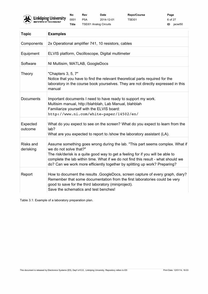
Topic Examples
Components 2x Operational amplifier 741, 10 resistors, cables
Equipment ELVIS platform, Oscilloscope, Digital multimeter
Software NI Multisim, MATLAB, GoogleDocs
Theory "Chapters 3, 5, 7"Notice that you have to find the relevant theoretical parts required for the laboratory in the course book yourselves. They are not directly expressed in this manual
Documents Important documents I need to have ready to support my work.Multisim manual, http://blahblah, Lab Manual, blahblahFamiliarize yourself with the ELVIS board: http://www.ni.com/whitepaper/14502/en/
Expected outcome
What do you expect to see on the screen? What do you expect to learn from the lab? What are you expected to report to /show the laboratory assistant (LA).
Risks and derisking
Assume something goes wrong during the lab. "This part seems complex. What ifwe do not solve that?"The risk/derisk is a quite good way to get a feeling for if you will be able to complete the lab within time. What if we do not find this result - what should we do? Can we work more efficiently together by splitting up work? Preparing?
Report How to document the results .GoogleDocs, screen capture of every graph, diary?Remember that some documentation from the first laboratories could be very good to save for the third laboratory (miniproject).Save the schematics and test benches!
Table 3.1: Example of a laboratory preparation plan.
This document is released by Electronics Systems (ES), Dep't of E.E., Linköping University. Repository refers to ES Print Date: 12/01/14, 16:03
No Rev Date Repo/Course Page
0001 P5A 2014-12-01 TSEI01 7 of 27
Title TSEI01 Analog Circuits ID jacwi50
-LAB1-
SIMULATION WITH SPICE
1 Introduction
In this first laboratory of the TSEI01 course you will simply get used to the simulator and the toolfrom National Instruments. The software is easily located under the Start menu (Windows 7),Programs, National Instruments, Design Suite.
Open the "Getting Started" [PDF] from the Help menu and simply follow the steps through it. Thedocument is called "NI Circuit Design Suite, Getting started NI Circuit Design Suite". (Notice thatthere are some different revisions of the document floating around if you would google for it).
✗ Go through chapter 1 and chapter 2 of the manual.
The latest version of the document can also be downloaded from
• http://www.ni.com/pdf/manuals/374482d.pdf
Supporting documents can also be videos and there are plenty of those in various flavours, e.g.:
• https://www.youtube.com/watch?v=tgCPDBtRcso • https://www.youtube.com/watch?v=pg4DI5s8FNo • https://www.youtube.com/watch?v=QVR86gaLhUc • https://www.youtube.com/watch?v=vZA47ojNOLs
This document is released by Electronics Systems (ES), Dep't of E.E., Linköping University. Repository refers to ES Print Date: 12/01/14, 16:03
No Rev Date Repo/Course Page
0001 P5A 2014-12-01 TSEI01 8 of 27
Title TSEI01 Analog Circuits ID jacwi50
some of these channels have more videos on how to simulate and operate the tool. Pop somepopcorn and watch some videos.
2 Examination
The examination of this first laboratory consists of two elements:
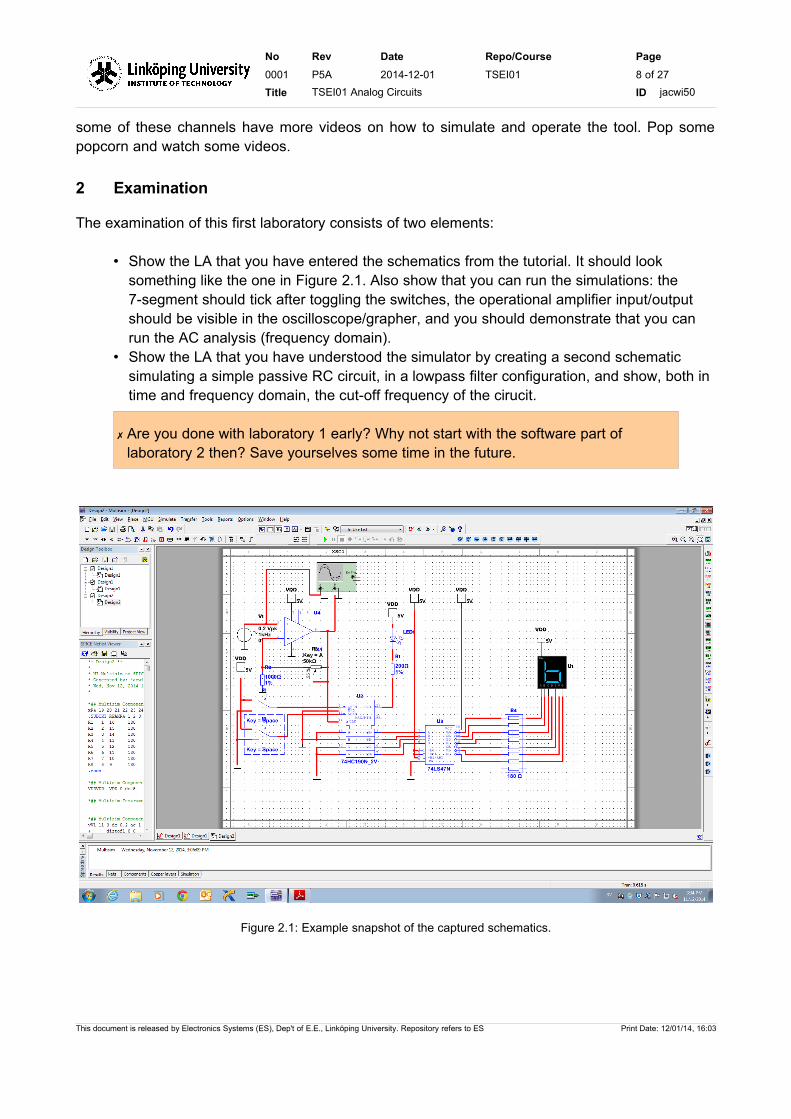
• Show the LA that you have entered the schematics from the tutorial. It should look something like the one in Figure 2.1. Also show that you can run the simulations: the 7-segment should tick after toggling the switches, the operational amplifier input/output should be visible in the oscilloscope/grapher, and you should demonstrate that you can run the AC analysis (frequency domain).
• Show the LA that you have understood the simulator by creating a second schematic simulating a simple passive RC circuit, in a lowpass filter configuration, and show, both in time and frequency domain, the cut-off frequency of the cirucit.
✗ Are you done with laboratory 1 early? Why not start with the software part of laboratory 2 then? Save yourselves some time in the future.
This document is released by Electronics Systems (ES), Dep't of E.E., Linköping University. Repository refers to ES Print Date: 12/01/14, 16:03
Figure 2.1: Example snapshot of the captured schematics.
No Rev Date Repo/Course Page
0001 P5A 2014-12-01 TSEI01 9 of 27
Title TSEI01 Analog Circuits ID jacwi50
-LAB2-
OPAMPS AND NEGATIVE
FEEDBACK
1 Introduction
In this laboratory we will look at different ways of feedback and compensation of your operationalamplifier in order to improve the overall performance of the system with respect to stability andlinearity. In Bengt Molin's book we can read a about the history of feedback and conclude that itwas surprisingly difficult to understand and introduce as a design concept for electrical circuits.Today, even though the maths can be a bit troublesome from time to time, we see it as a quitenatural way of stabilizing a circuit.
The task of this laboratory is to
✗ Dimension the feedback in a three-stage amplifier (using operational amplifiers) such that the total phase margin is ϕm=45 degrees.
✗ The compensated amplifier's frequency and step responses should be simulated and also measured.
In the first part of the laboratory you will simulate an electronic circuit using a set of operationalamplifiers. You will investigate how feedback can be applied and what the consequences are.
This document is released by Electronics Systems (ES), Dep't of E.E., Linköping University. Repository refers to ES Print Date: 12/01/14, 16:03
No Rev Date Repo/Course Page
0001 P5A 2014-12-01 TSEI01 10 of 27
Title TSEI01 Analog Circuits ID jacwi50
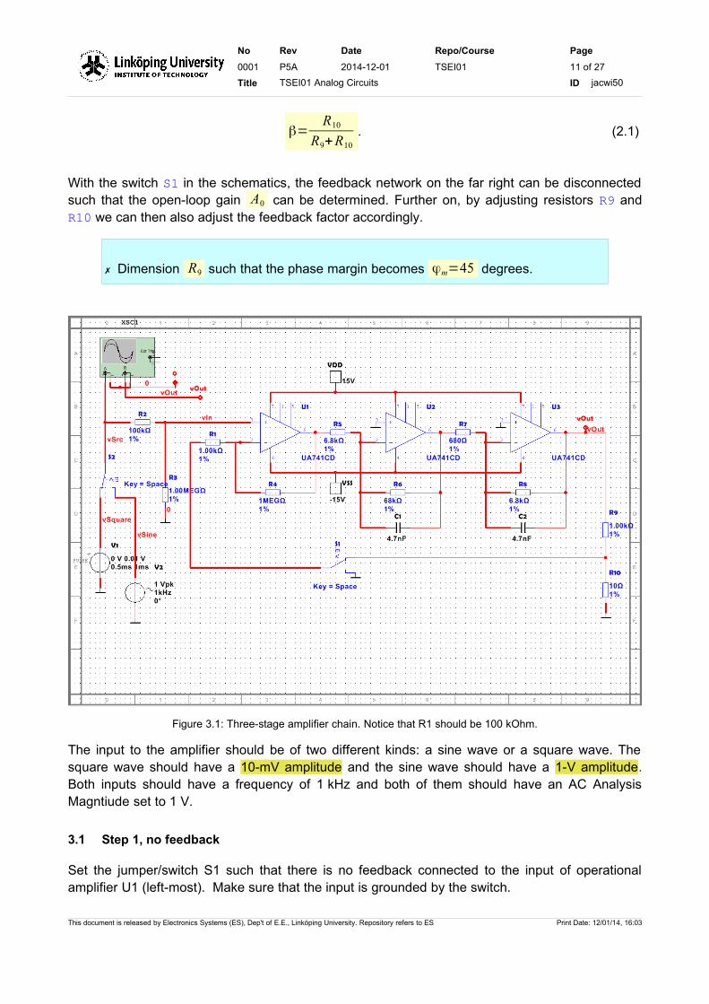
The circuit schematic is given to you and can be downloaded from the course webpage:
http://www.isy.liu.se/edu/kurs/TSEI01/laboration/TSEI01_PM_laboratory2.ms12
and reprinted in Figure 3.1 as it looks in the simulator.
In the second part of the laboratory you will also set up the design in a hardware test bench andevaluate it in "real life".
✗ Tip! You are most likely two people in the lab group. Save yourself some time: one of you will setup the simulator and one of you will start arranging with the hardware platform and connect the circuits. The laboratory assistant provides you with components.
2 Preparations
Do not forget to hand in your lab preparation plan! Suggestions on topics to plan are found inTable 3.1. In this laboratory the following things could be discussed (examples)
• Phase margin. What is the concept of phase margin and what is the impact on e.g. the step-response of your amplifier?
• DC gain. What is the total DC gain, in open-loop configuration, of the amplifier in Figure 3.1?
• Feedback factor. What is the relationship between feedback factor and gain, phase margin, and amplitude margin?
• Download datasheets, read chapters in book, refresh lecture notes and lesson exercises.
and more.
3 Simulation setup and running the simulations
As mentioned, the amplifier schematics is shown in Figure 2.1. As you see we have preparedmost of the schematics for you, but the feedback (right-most part) is not really dimensioned as itshould be.
Notice the type of operational amplifier (UA741CD). Datasheets for that particular type are foundon the web and you would there also find descriptions of the pin-outs, open-loop gain, and anyother parameter that might be vital for you.
In this case, the feedback factor β is essentially given by how much voltage is fed back from theoutput to the input of the amplifier by using the resistive divider:
This document is released by Electronics Systems (ES), Dep't of E.E., Linköping University. Repository refers to ES Print Date: 12/01/14, 16:03
No Rev Date Repo/Course Page
0001 P5A 2014-12-01 TSEI01 11 of 27
Title TSEI01 Analog Circuits ID jacwi50
β=R10
R9+R10. (2.1)
With the switch S1 in the schematics, the feedback network on the far right can be disconnectedsuch that the open-loop gain A0 can be determined. Further on, by adjusting resistors R9 andR10 we can then also adjust the feedback factor accordingly.
✗ Dimension R9 such that the phase margin becomes ϕm=45 degrees.
The input to the amplifier should be of two different kinds: a sine wave or a square wave. Thesquare wave should have a 10-mV amplitude and the sine wave should have a 1-V amplitude.Both inputs should have a frequency of 1 kHz and both of them should have an AC AnalysisMagntiude set to 1 V.
3.1 Step 1, no feedback
Set the jumper/switch S1 such that there is no feedback connected to the input of operationalamplifier U1 (left-most). Make sure that the input is grounded by the switch.
This document is released by Electronics Systems (ES), Dep't of E.E., Linköping University. Repository refers to ES Print Date: 12/01/14, 16:03
Figure 3.1: Three-stage amplifier chain. Notice that R1 should be 100 kOhm.
No Rev Date Repo/Course Page
0001 P5A 2014-12-01 TSEI01 12 of 27
Title TSEI01 Analog Circuits ID jacwi50
When you dimension the feedback you should set R10=10 and R9 should eventually be a valuetaken from the standard E12 series [browse the web to find this table of values]. Start your firsttrials to understand the circuit and check its functionality with a sine wave input signal at a 1-kHzfrequency and a 1-V amplitude.
Start the simulation and observe the input and output waveforms in the time-domain by doubleclicking the oscilloscope.
✗ What happens with the output signal vOut?
Now configure an AC analysis in the following way.
Simulate > Analyses > AC Analysis...Frequency ParametersStart frequency (FSTART): 1 HzStop frequency (FSTOP): 100 MHzSweep type: decadeNumber of points per decade: 100Vertical scale: logarithmicOutputV(vOut) > Add >Simulate
Table 3.1: AC analysis settings.
The grapher view window pops up and you can see the magnitude function and the phasediagram, essentially your Bode plot.
✗ We will determine the feedback factor β for a phase margin of ϕm=45 degrees.
To establish the feedback factor, we first find the point where the phase is −180−ϕm=135degrees. In the grapher viewer you can select cursors and add to both the magnitude graph aswell as the phase graph. In the phase diagram pull one of them to ϕ=−135 . Find the frequencyfor which this happens, i.e., the x-value. (Yes, the values in the small white box are a bit cryptical,but move the cursor back and forth and you will see which cursor is affecting which value).
✗ What x-value, i.e., frequency, do you get?
Now, determine the open-loop gain A0 when the phase is at ϕ=−135 . This can be done byplacing the mouse pointer in the magnitude diagram and move the cursors to the same x-valuefrequency.
This document is released by Electronics Systems (ES), Dep't of E.E., Linköping University. Repository refers to ES Print Date: 12/01/14, 16:03
No Rev Date Repo/Course Page
0001 P5A 2014-12-01 TSEI01 13 of 27
Title TSEI01 Analog Circuits ID jacwi50
✗ What A0 value do you get for the point where ϕ=−135 ?
According to theory (you have read the chapters in the book?) we should now let the feedbackfactor be a function of the amplitude margin
β=1A0
(c.f. amplitude margin) and β=R10
R9+R10(2.2)
which, if we assume R10=10 , can give us the value of R9 . Round the value to the closest valuein the E12 series.
✗ Which R9 value do you get?
✗ Which value do you take from the E12 series?
3.2 Step 2, with feedback
Now set jumper/switch in a position such that feedback is guaranteed and apply the feedbacksettings derived from the previous part of the lab.
Re-run the simulation and observe the results in both time domain and frequency domain.
✗ What overall DC gain do you get?
✗ What bandwidth?
✗ What unity-gain frequency do you get?
✗ What does the sinusoid look like now?
Toggle the input signal to use a pulse train with a 1-kHz frequency and 10-mV swing and run atransient analysis. In this case use the grapher viewer rather than the oscilloscope. The settingsare found in Table 3.2.
Apply a step response and observe and capture the behavior.
✗ How large is the overshoot? How does this correspond to theory?
This document is released by Electronics Systems (ES), Dep't of E.E., Linköping University. Repository refers to ES Print Date: 12/01/14, 16:03
No Rev Date Repo/Course Page
0001 P5A 2014-12-01 TSEI01 14 of 27
Title TSEI01 Analog Circuits ID jacwi50
Simulate > Analyses > Transient Analysis ...
Analysis parametersInitial Conditions User definedStart Time (TSTART) 0End Time (TSTOP) 0.002 sMaximum time step (TMAX)Minimum number of time points 1000
OutputV(vOut)> Add >
Simulate
Table 3.2: Transient analysis settings.
3.3 Intermediate examination
Before you get too wild you might want to double check with the laboratory assistant that you haveeverything set up correctly in order to continue with the hardware lab (Section 4).
✗ Reasonable value on R9 found?
✗ All the questions in the blue boxes answered?
This document is released by Electronics Systems (ES), Dep't of E.E., Linköping University. Repository refers to ES Print Date: 12/01/14, 16:03
No Rev Date Repo/Course Page
0001 P5A 2014-12-01 TSEI01 15 of 27
Title TSEI01 Analog Circuits ID jacwi50
4 Measurements, i.e., the hardware part
You now also have to measure the amplifier setup in real life. For this purpose you will use theELVIS+ board. There is plenty of information on the web about the platform as well as tutorials onNational Instruments home page and included also in the software. We will not repeat them in thisdocument, nor will we describe the way a component is physically placed in detail. Trial-and-erroris a good strategy also here. The ELVIS+ board is more or less bullet-proof and it is easy topick-and-place components and move them around. If you by accident short to signals, ELVIS willnot mind.
✗ Read more about the hardware platform! Identify components, knobs, buttons, what-have-you on the board. Notice that there are two ON-buttons.
✗ Understand how all the holes on the ELVIS+ board are connected "underneath".
Once you have a pretty good understanding, you will start to connect your amplifier, more or lessas it is shown in Figure 3.1, on the board by placing all the components. Jumpers/switches are ofcourse not there, supplies and signals are taken from the ELVIS+. The oscilloscope is alsoprovided to you by the ELVIS+ board.
✗ Show the assistant that you have ELVIS+ up and running and then ask the laboratory assistant for components that you need to hook up your circuit.
The most complex component is probably the operation amplifier and you need search for theUA741CD component on the internet to find the pin-out, for example
• http://cdn.instructables.com/FXE/J8RT/GAFDTBQ1/FXEJ8RTGAFDTBQ1.LARGE.gif
or simply the datasheet from the hardware provider. At this point in the laboratory series, youprobably do not have to care for the offset adjustment pins (5 and 1) unless your specific sampleof operational amplifier happens to have bad quality. The supplies should connect to the fixed+15/-15 available on the ELVIS+ board. Use the long +/- vertical rails to distribute the voltagesacross your design.
4.1 Connecting the cables
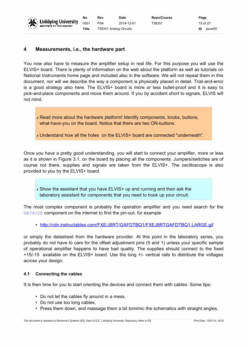
It is then time for you to start orienting the devices and connect them with cables. Some tips:
• Do not let the cables fly around in a mess. • Do not use too long cables, • Press them down, and massage them a bit tomimic the schematics with straight angles.
This document is released by Electronics Systems (ES), Dep't of E.E., Linköping University. Repository refers to ES Print Date: 12/01/14, 16:03
No Rev Date Repo/Course Page
0001 P5A 2014-12-01 TSEI01 16 of 27
Title TSEI01 Analog Circuits ID jacwi50
• Do not use cables for interconnects provided to you locally by the board. • Use color-coded cables, supply/ground/input/output
Figure 4.1.1 shows some bad and good examples for inspiration. Use common sense and createa circuit that you can proudly present: "this is my design".
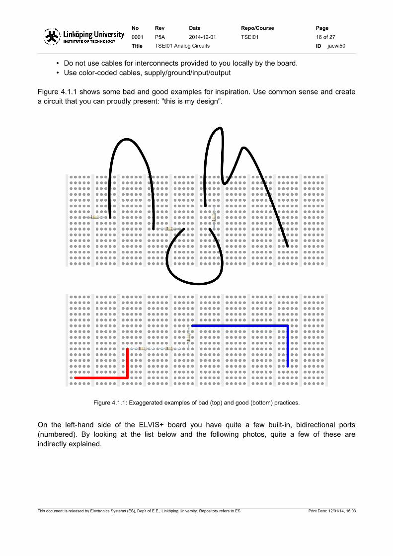
On the left-hand side of the ELVIS+ board you have quite a few built-in, bidirectional ports(numbered). By looking at the list below and the following photos, quite a few of these areindirectly explained.
This document is released by Electronics Systems (ES), Dep't of E.E., Linköping University. Repository refers to ES Print Date: 12/01/14, 16:03
Figure 4.1.1: Exaggerated examples of bad (top) and good (bottom) practices.
No Rev Date Repo/Course Page
0001 P5A 2014-12-01 TSEI01 17 of 27
Title TSEI01 Analog Circuits ID jacwi50
Connect them according to this:
✗ Obviously there are many ways to connect input and output signals, but in our case,to simplify debugging if needed, please use the same settings as recommended in the lab manual.
• AI0+ (row 1) should be connected to the function generator (FGEN, row 33)• AI0 (row 2) should be connected to ground (AIGND, row 18)• AI1+ (row 3) should be connected to the output of the amplifier, vOut in Figure 3.1.• AI1 (row 4) should be connected to ground (AIGND, row 18)• AI0+ (row 1) should also be connected to the input of your amplifier, i.e., vSrc in Figure
3.1.
This document is released by Electronics Systems (ES), Dep't of E.E., Linköping University. Repository refers to ES Print Date: 12/01/14, 16:03
Figure 4.1.2: Photo of the ELVIS+ board top left pin-out.
No Rev Date Repo/Course Page
0001 P5A 2014-12-01 TSEI01 18 of 27
Title TSEI01 Analog Circuits ID jacwi50
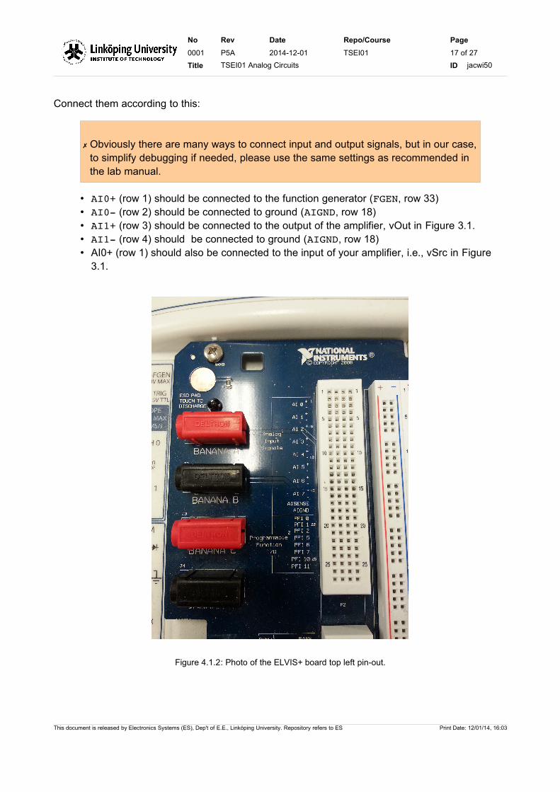
Verify that
• FGEN (row 33) is connected to AI0+ (row 1) and the input of the amplifier.• Power supplies (positive and negative) and ground to the amplifiers are found on rows 51,
52, and 53.
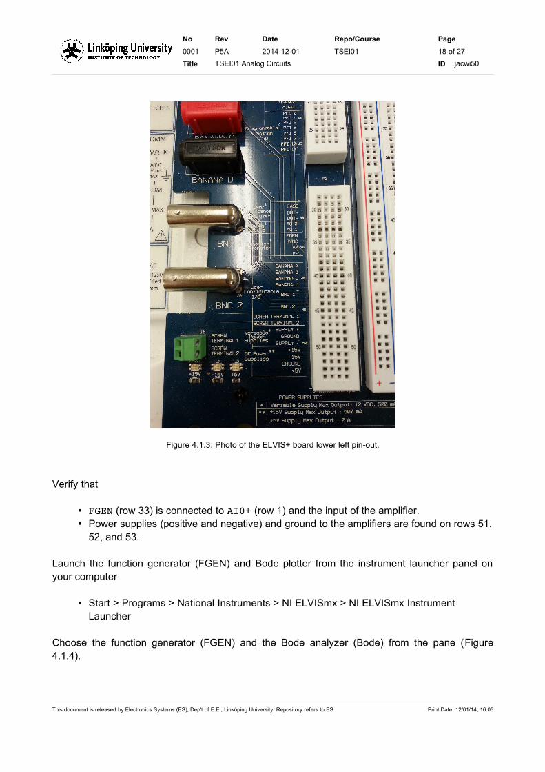
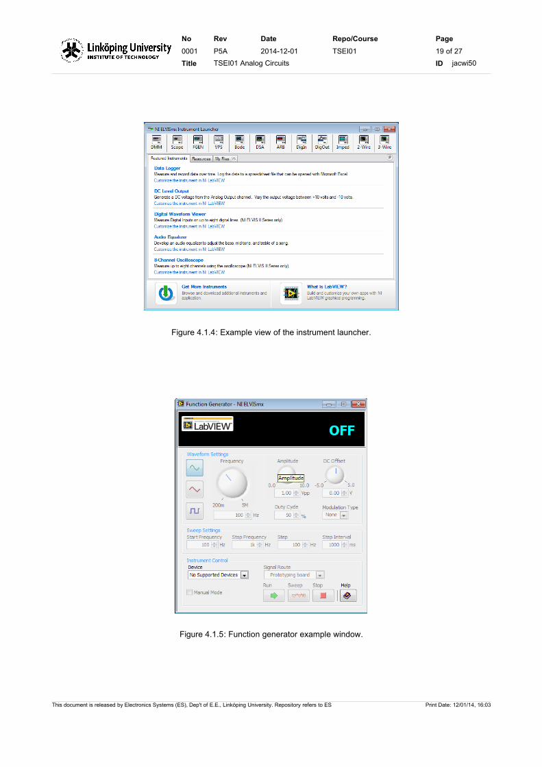
Launch the function generator (FGEN) and Bode plotter from the instrument launcher panel onyour computer
• Start > Programs > National Instruments > NI ELVISmx > NI ELVISmx Instrument Launcher
Choose the function generator (FGEN) and the Bode analyzer (Bode) from the pane (Figure4.1.4).
This document is released by Electronics Systems (ES), Dep't of E.E., Linköping University. Repository refers to ES Print Date: 12/01/14, 16:03
Figure 4.1.3: Photo of the ELVIS+ board lower left pin-out.
No Rev Date Repo/Course Page
0001 P5A 2014-12-01 TSEI01 19 of 27
Title TSEI01 Analog Circuits ID jacwi50
This document is released by Electronics Systems (ES), Dep't of E.E., Linköping University. Repository refers to ES Print Date: 12/01/14, 16:03
Figure 4.1.4: Example view of the instrument launcher.
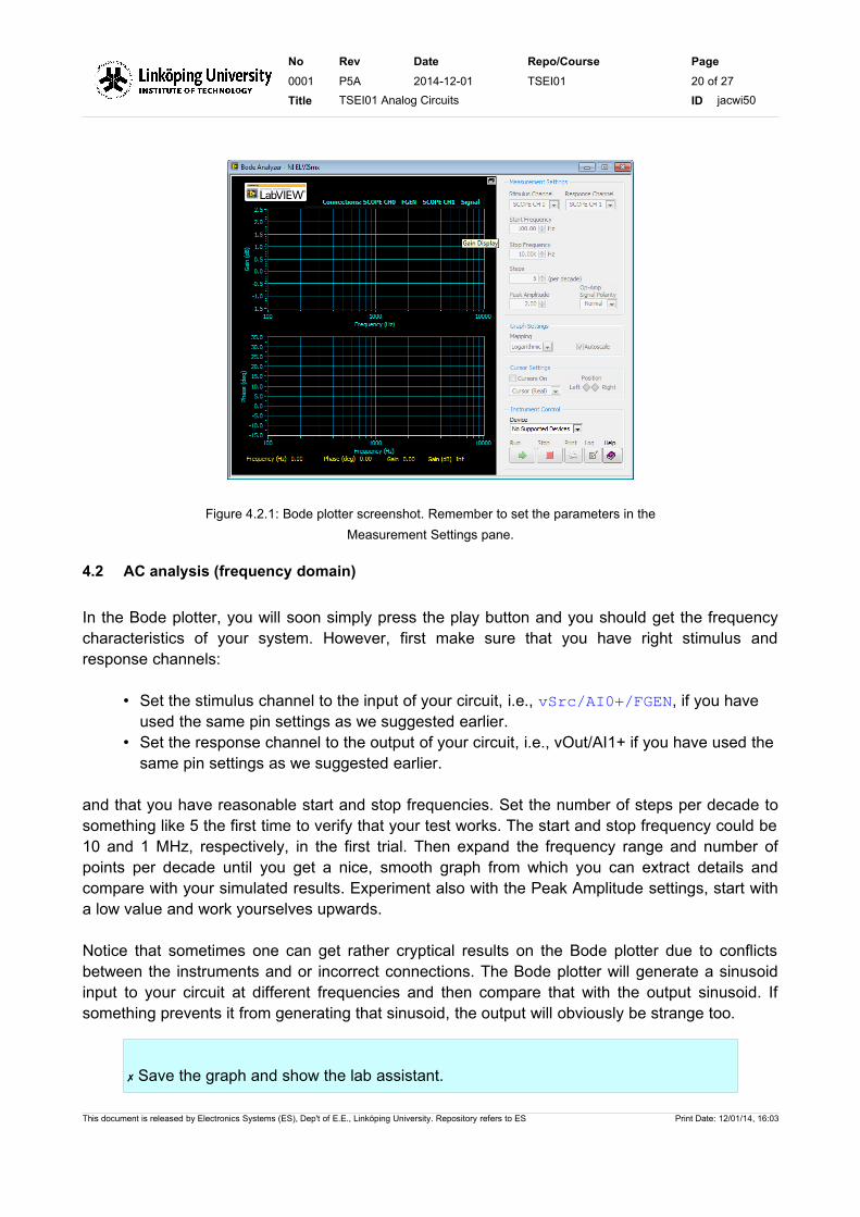
Figure 4.1.5: Function generator example window.
No Rev Date Repo/Course Page
0001 P5A 2014-12-01 TSEI01 20 of 27
Title TSEI01 Analog Circuits ID jacwi50
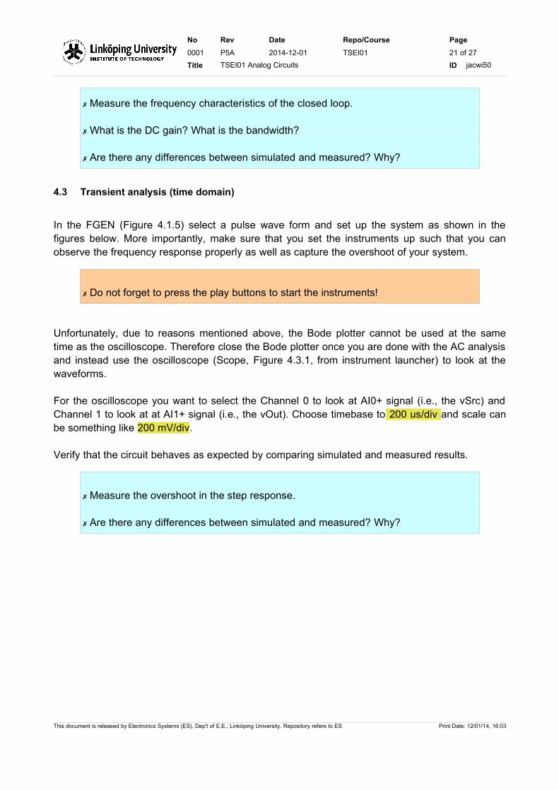
4.2 AC analysis (frequency domain)
In the Bode plotter, you will soon simply press the play button and you should get the frequencycharacteristics of your system. However, first make sure that you have right stimulus andresponse channels:
• Set the stimulus channel to the input of your circuit, i.e., vSrc/AI0+/FGEN, if you have used the same pin settings as we suggested earlier.
• Set the response channel to the output of your circuit, i.e., vOut/AI1+ if you have used the same pin settings as we suggested earlier.
and that you have reasonable start and stop frequencies. Set the number of steps per decade tosomething like 5 the first time to verify that your test works. The start and stop frequency could be10 and 1 MHz, respectively, in the first trial. Then expand the frequency range and number ofpoints per decade until you get a nice, smooth graph from which you can extract details andcompare with your simulated results. Experiment also with the Peak Amplitude settings, start witha low value and work yourselves upwards.
Notice that sometimes one can get rather cryptical results on the Bode plotter due to conflictsbetween the instruments and or incorrect connections. The Bode plotter will generate a sinusoidinput to your circuit at different frequencies and then compare that with the output sinusoid. Ifsomething prevents it from generating that sinusoid, the output will obviously be strange too.
✗ Save the graph and show the lab assistant.
This document is released by Electronics Systems (ES), Dep't of E.E., Linköping University. Repository refers to ES Print Date: 12/01/14, 16:03
Figure 4.2.1: Bode plotter screenshot. Remember to set the parameters in the
Measurement Settings pane.
No Rev Date Repo/Course Page
0001 P5A 2014-12-01 TSEI01 21 of 27
Title TSEI01 Analog Circuits ID jacwi50
✗ Measure the frequency characteristics of the closed loop.
✗ What is the DC gain? What is the bandwidth?
✗ Are there any differences between simulated and measured? Why?
4.3 Transient analysis (time domain)
In the FGEN (Figure 4.1.5) select a pulse wave form and set up the system as shown in thefigures below. More importantly, make sure that you set the instruments up such that you canobserve the frequency response properly as well as capture the overshoot of your system.
✗ Do not forget to press the play buttons to start the instruments!
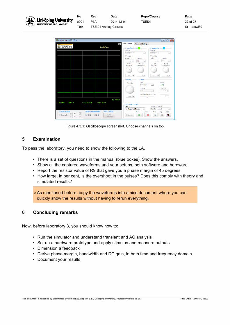
Unfortunately, due to reasons mentioned above, the Bode plotter cannot be used at the sametime as the oscilloscope. Therefore close the Bode plotter once you are done with the AC analysisand instead use the oscilloscope (Scope, Figure 4.3.1, from instrument launcher) to look at thewaveforms.
For the oscilloscope you want to select the Channel 0 to look at AI0+ signal (i.e., the vSrc) andChannel 1 to look at at AI1+ signal (i.e., the vOut). Choose timebase to 200 us/div and scale canbe something like 200 mV/div.
Verify that the circuit behaves as expected by comparing simulated and measured results.
✗ Measure the overshoot in the step response.
✗ Are there any differences between simulated and measured? Why?
This document is released by Electronics Systems (ES), Dep't of E.E., Linköping University. Repository refers to ES Print Date: 12/01/14, 16:03
No Rev Date Repo/Course Page
0001 P5A 2014-12-01 TSEI01 22 of 27
Title TSEI01 Analog Circuits ID jacwi50
5 Examination
To pass the laboratory, you need to show the following to the LA.
• There is a set of questions in the manual`(blue boxes). Show the answers.• Show all the captured waveforms and your setups, both software and hardware.• Report the resistor value of R9 that gave you a phase margin of 45 degrees.• How large, in per cent, is the overshoot in the pulses? Does this comply with theory and
simulated results?
✗ As mentioned before, copy the waveforms into a nice document where you can quickly show the results without having to rerun everything.
6 Concluding remarks
Now, before laboratory 3, you should know how to:
• Run the simulator and understand transient and AC analysis• Set up a hardware prototype and apply stimulus and measure outputs• Dimension a feedback• Derive phase margin, bandwidth and DC gain, in both time and frequency domain• Document your results
This document is released by Electronics Systems (ES), Dep't of E.E., Linköping University. Repository refers to ES Print Date: 12/01/14, 16:03
Figure 4.3.1: Oscilloscope screenshot. Choose channels on top.
No Rev Date Repo/Course Page
0001 P5A 2014-12-01 TSEI01 23 of 27
Title TSEI01 Analog Circuits ID jacwi50
-LAB3-
RIAA AMPLIFIER STAGES
1 Introduction
In modern stereo amplifiers you rarely find an analog input for a record player (phono) any more.Your exercise is therefore to design and build an RIAA-compensated2 amplifier which then can beconnected between the record player and the normal line input of the stereo.
✗ Notice that in this lab, you will not find the schematic per se in this manual, but a strategic search for e.g. "non-inverting shelving filters" would be a good start.
You will design an amplifier containing three amplifier stages. The first stage should be atransistor-based stage. The second and third should be opamp-based. It would also be practicalto use two operational amplifier stages that are architecturally identical, but with differentcomponent values. Even though it is not optimum from a noise point of view, set them to have thesame gain (approximately).
✗ Work in parallel! You are at least two people in the group - work in parallel to speed up the process and improve the learning curve.
2Search on the internet why an equalization is needed - it is quite a fascinating story.
This document is released by Electronics Systems (ES), Dep't of E.E., Linköping University. Repository refers to ES Print Date: 12/01/14, 16:03
No Rev Date Repo/Course Page
0001 P5A 2014-12-01 TSEI01 24 of 27
Title TSEI01 Analog Circuits ID jacwi50
2 Specification
For the RIAA equalization (once again search on the web resources for a closer description) werequire the following specification:
• Input sensitivity: 1 mV• Input resistance: > 4 kOhm• Total gain at low frequencies: 64 dB• Output resistance: < 1 kOhm• Supply voltages: -/+ 15 V
• The amplifier should be designed with - in mentioned order - one transistor stage (NPN, BC546B) and two operational amplifier stages (UA741CD).
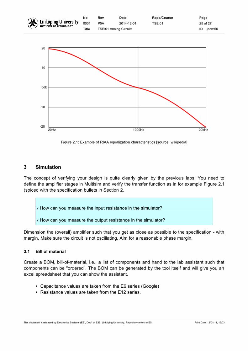
The RIAA compensation/equalization, i.e., placement of important poles and zeros, should beaccomplished with the operational amplifier stages (i.e., do not include the single-transistor stagein this case). See Figure 2.1 for an example of the RIAA equalization curve. It is perhaps not veryobvious from this picture, but it contains two poles and one zero.
✗ Where are the poles and zero located in the RIAA equalization curve?
✗ How do you guarantee the specified output resistance?
The rest of the gain and suitable input resistance is accomplished by the transistor stage, i.e., thetransistor stage should be placed at the input of your design.
• Use the BC546B BJT transistor • Use the uA741 operational amplifier.
✗ Think of how you should isolate the potential DC offsets between amplifier stages (where applicable)!
✗ The design must first be verified in the simulator, otherwise debugging can become very, very tedious.
This document is released by Electronics Systems (ES), Dep't of E.E., Linköping University. Repository refers to ES Print Date: 12/01/14, 16:03
No Rev Date Repo/Course Page
0001 P5A 2014-12-01 TSEI01 25 of 27
Title TSEI01 Analog Circuits ID jacwi50
3 Simulation
The concept of verifying your design is quite clearly given by the previous labs. You need todefine the amplifier stages in Multisim and verify the transfer function as in for example Figure 2.1(spiced with the specification bullets in Section 2.
✗ How can you measure the input resistance in the simulator?
✗ How can you measure the output resistance in the simulator?
Dimension the (overall) amplifier such that you get as close as possible to the specification - withmargin. Make sure the circuit is not oscillating. Aim for a reasonable phase margin.
3.1 Bill of material
Create a BOM, bill-of-material, i.e., a list of components and hand to the lab assistant such thatcomponents can be "ordered". The BOM can be generated by the tool itself and will give you anexcel spreadsheet that you can show the assistant.
• Capacitance values are taken from the E6 series (Google)• Resistance values are taken from the E12 series.
This document is released by Electronics Systems (ES), Dep't of E.E., Linköping University. Repository refers to ES Print Date: 12/01/14, 16:03
Figure 2.1: Example of RIAA equalization characteristics [source: wikipedia]
No Rev Date Repo/Course Page
0001 P5A 2014-12-01 TSEI01 26 of 27
Title TSEI01 Analog Circuits ID jacwi50
4 Measurements
You have access to the positive and negative +/-15 V supplies on the ELVIS+ board.
In the measurements verify the functionality with sine wave generator (FGEN) in ELVIS+ and theBode plotter. Very same way as you did in Lab 2.
Once you have verified that theory, simulation, and measurements agree, ask the lab assistant forhelp to connect your amplifier to the stereo such that your design can be compared to a referenceamplifier.
5 Resources
Much of the information is most conveniently found on the internet.
• Google: RIAA equalization Bode plot
• http://www.onsemi.com/pub_link/Collateral/BC546-D.PDF
• http://pdf.datasheetcatalog.com/datasheet/philips/BC546_547_3.pdf
• http://www.ti.com/lit/ds/symlink/lm741.pdf
6 Examination
6.1 Step 1
In order to avoid coming back to the lab on off-hours in case something was forgotten, you wouldhave to show your intermediate results such that the lab assistant can guide you towards a robustdesign (i.e., show the BOM).
Further on, address the blue boxes in the manual.
In order to eventually pass the laboratory/mini project, the amplifier must work sufficiently goodand a report must be handed it containing schematics, chosen values, measured and simulatedresults as well as motivation, conclusions, etc. See below.
7 Report template
There is no template for the report. You have to convince the examiner that you should pass thecourse. However, one should obviously follow good writing procedures, such as for example:
• http://www.liu.se/cmts/kursutbudet/tfke33/lathund-for-rapportskrivning/1.71024/Lathund200 6-01-20.pdf
This document is released by Electronics Systems (ES), Dep't of E.E., Linköping University. Repository refers to ES Print Date: 12/01/14, 16:03
No Rev Date Repo/Course Page
0001 P5A 2014-12-01 TSEI01 27 of 27
Title TSEI01 Analog Circuits ID jacwi50
Make sure to document as much as possible. Take window snapshots and save graphs, etc., toinclude in the report. You have to supply theoretical results, simulated results, and measuredresults. You should also comment on the audio quality.
✗ Insert an executive summary of your results on the first page of your report!
This document is released by Electronics Systems (ES), Dep't of E.E., Linköping University. Repository refers to ES Print Date: 12/01/14, 16:03