Embed Size (px)
Citation preview

TSEA44: Computer hardware – a system on a chipKent Palmkvist, Erik Bertilssonhttp://www.isy.liu.se/edu/kurs/TSEA44Based on slides by Andreas Ehliar
What is the course about?● How to build a complete embedded computer using an
FPGA and a few other components. Why?– Only one chip– The computer can easily be tailored to your needs.
● Special instructions● Accelerators● DMA transfer
– The computer can be simulated– A logic analyzer can be added in the FPGA
● Add performance counters– It's fun!
2017-10-30 2TSEA44: Computer hardware – a system on a chip
Prerequisites (expected knowledge!)● Digital logic design. You will design both a data path and a
control unit for an accelerator.● Binary arithmetic. Signed/unsigned numbers.● VHDL or Verilog. SystemVerilog (SV) is the language used
in the course.● Computer Architecture. It is extremely important to
understand how a CPU executes code. You will also design part of a DMA-controller. Bus cycles are central.
● ASM and C programming. Most of the programming is done in C, with a few cases of inline asm.
2017-10-30 3TSEA44: Computer hardware – a system on a chip
Course organisation● Lab 0: learn enough Verilog, 4 hours
– Individual work and demonstration● Lab course: 4 mini projects
– 6 groups * 3 students in the lab● Lectures: 8*2 hours
– 1 guest lecture from ARM● Examination 6 credits:
– 3 written reports/group
– Oral individual questions
2017-10-30 4TSEA44: Computer hardware – a system on a chip
10/30/2017 22:32

Lab course is based on an application2004 - trackingwww.robocup.org/2012/06/robocup-the-small-sized-league/
Funny/impressive youtube video available
2017-10-30 5TSEA44: Computer hardware – a system on a chip
5
cameraour FPGA computer
1 robotB/W
VGA
Lab course is based on an application2015-17 – JPEG compression
● Take 2-D DCT on 8x8-blocks● Quantize = Divide and set small values to zero● RLE + Huffman code
2017-10-30 6TSEA44: Computer hardware – a system on a chip
CPUbitfield instr.
• 2-D DCT acc• Quantization• DMA
I/O camera
eth
Acc.
Memtestbild.raw -> testbild.jpg
Lab info● 0) Build an UART in Verilog● 1) Interface your UART
Test performance counters Test a SW-DCT2 application
● 2+3) Build an HW accelerator for 2-D DCT and add a DMA controller
● 4) Design your own instruction to handle bitfields
2017-10-30 7TSEA44: Computer hardware – a system on a chip
FPGA CPU
bit instr.
2-D DCTQuantization
DMA
UART
eth
mem
Lab tasks and examination● Lab 0 (individual work and demonstration)
– Build an UART in Verilog
– Demonstration
– Deadline 10 November● Lab 1 (in groups of 2 or 3 students)
– Interface to the Wishbone bus
– Demonstration (individual questions)Written report
2017-10-30 8TSEA44: Computer hardware – a system on a chip
10/30/2017 22:32
Lab tasks and examination, cont.● Lab 2+3
– Design a JPEG accelerator + DMA
– Demonstration (with individual questions)Written report
● Lab 4
– Custom Instruction
– Demonstration (with individual questions)Written report
2017-10-30 9TSEA44: Computer hardware – a system on a chip
Written report requirements● A readable short report typically consisting of
– Introduction
– Design, where you explain with text and diagrams how your design works
– Results, that you have measured
– Conclusions
– Appendix: All Verilog and C code with comments!
2017-10-30 10TSEA44: Computer hardware – a system on a chip
Competition – fastest JPEG compression● An unaccelerated JPEG compression
(using jpegfiles) takes roughly 13.0 Mcycles (@ 25MHz) 2 FPS (Frames ≃Per Second)
● Our record: ~ 100 000 cycles (everything in hardware)
● Goal: Highest framrate. Exception: At over 25 FPS, the smallest implementation wins
● Deadline: 19/12 2017
2017-10-30 11TSEA44: Computer hardware – a system on a chip
wunderb.jpg320 x 240
The hardware, lab0● Zedboard
– Programming connection attop of the board
– Serial port at bottom of the board
– Only use PL part ofof the chip
2017-10-30 12TSEA44: Computer hardware – a system on a chip
10/30/2017 22:32

The hardware, lab0 - lab4● 6 boxes with FPGA boards
–
2017-10-30 13TSEA44: Computer hardware – a system on a chip
The soft computer● OR1200 CPU● Memory
– RAM (+ SDRAM)
– ROM (+ FLASH)● I/O
– Serial
– Parallel
– Ethernet
– Camera
2017-10-30 14TSEA44: Computer hardware – a system on a chip
Opencores● Open source
initiative for hardwaremodels
● From simple to very complex models
● Note page is showing only FPGA proven LGPL licensed models
2017-10-30 15TSEA44: Computer hardware – a system on a chip
Processor core: Openrisc 1200● Initially developed within opcores initiative● Split into a new website
– Openrisc.io● Complete risc processor including synthesizable code,
instructions set simulator etc.
2017-10-30 16TSEA44: Computer hardware – a system on a chip
10/30/2017 22:32

(System)Verilog● The course uses SystemVerilog● SystemVerilog is easy to learn if you know VHDL/C● Our soft computer (80% downloaded from OpenCores) is
written in Verilog● It is possible to use both languages in a design● You need to understand parts of the computer
2017-10-30 17TSEA44: Computer hardware – a system on a chip
(System)Verilog vs VHDLAn edge-trigged D-flip/flop
2017-10-30 18TSEA44: Computer hardware – a system on a chip
d q
clk
C-like syntax
module dff( input clk, d, output reg q);
always_ff @(posedge clk)q <= d;
endmodule
Ada-like syntax
entity dff isport (clk,d : in std_logic; q: out std_logic);end dff;
architecture firsttry of dff is beginprocess (clk) begin if rising_edge(clk) then q <= d; end if;end process;end firsttry;
(System)Verilog vs VHDLUsing the D-flip/flop, instantiation
2017-10-30 19TSEA44: Computer hardware – a system on a chip
// instantiation
wire a,b,c,grr;...
dff ff1(.clk(c),.d(a), .q(grr));
dff ff2(.clk(c), .d(grrr), .q(b));
d qac
bd qff2 ff2
grr
Watch out! Verilog allows implicit declarations (but this can be disabled)
You get a lab skeleton● dafk_tb.sv . Testbench.
– dafk_top.sv . To be synthesized in the FPGA. – eth_top.sv. Ethernet controller.– pkmc_top.sv. Memory controller.– or1200_top.sv. The OR1200 CPU.– parport.sv. Simple parallel port.– romram.sv . The boot code resides here.– uart_top.sv . UART 16550.– dvga_top.sv . VGA controller.– wb_top.sv . The wishbone bus.
– eth_phy.v Simulation model for the PHY chip.– flash.v Simulation model.– sdram.v Simulation model.– sram.v . Simulation model
2017-10-30 20TSEA44: Computer hardware – a system on a chip
10/30/2017 22:32
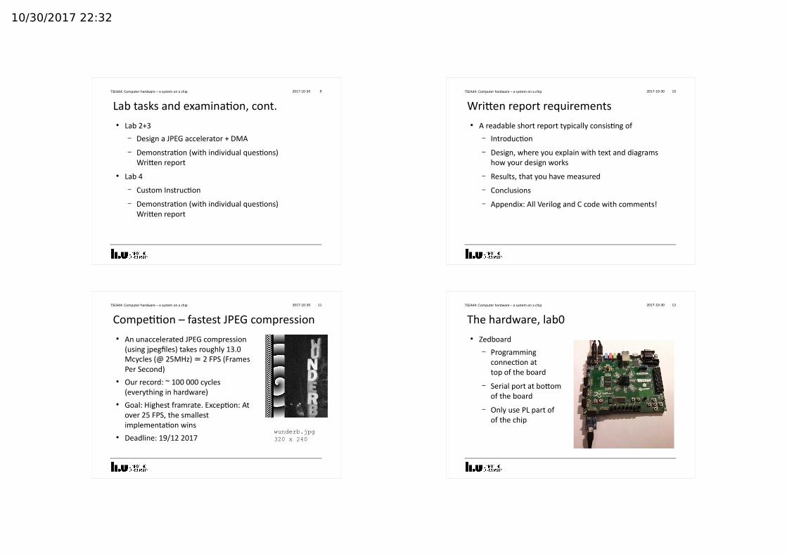
The Wishbone bus● A multi-master bus
– Signals: adress (32), data_out (32), data_in (32), control
– Two data buses and muxes are used instead of tristate
2017-10-30 21TSEA44: Computer hardware – a system on a chip
M0
M1
S0
S1
S2
CPU
The environment2017-10-30 22TSEA44: Computer hardware – a system on a chip
eth
Home directory
Fileserver
130.236.x.y
LinuxXilinx ISEModelSimgtktermTFTPmake simmake dafkor32-uclinux-gccprecision
pc 192.168.0.n
FPGAmonitor(rs232)uClinux * tftp * jpegtest
192.168.0.m
rs232
ProgrammingCable IV
130.236.z.w
Host
Board
Software under linux● C-compiler (GNU tool chain)
– or-32-uclinux-gcc● Software simulator
– or-32-uclinux-sim● A very simple boot monitor (24 kB
+ 8 kB RAM inside FPGA)
– dct_sw, dma_dct_sw, jpegtest● uClinux boots from flash
– jpegtest
2017-10-30 23TSEA44: Computer hardware – a system on a chip
host
board
Booting uClinux
2017-10-30 24TSEA44: Computer hardware – a system on a chip
uClinux/OR32Flat model support (C) 1998,1999 Kenneth Albanowski, D. Jeff DionneCalibrating delay loop.. ok - 2.00 BogoMIPSMemory available: 53000k/62325k RAM, 0k/0k ROM (667892k kernel data, 2182k code)Swansea University Computer Society NET3.035 for Linux 2.0NET3: Unix domain sockets 0.13 for Linux NET3.035.Swansea University Computer Society TCP/IP for NET3.034IP Protocols: ICMP, UDP, TCPuClinux version 2.0.38.1pre3 (olles@kotte) (gcc version 3.2.3) #180 Sat Sep 11 09:01:55 CEST 2004Serial driver version 4.13p1 with no serial options enabledttyS00 at 0x90000000 (irq = 2) is a 16550ARamdisk driver initialized : 16 ramdisks of 2048K sizeBlkmem copyright 1998,1999 D. Jeff DionneBlkmem copyright 1998 Kenneth AlbanowskiBlkmem 0 disk images:loop: registered device at major 7eth0: Open Ethernet Core Version 1.0RAMDISK: Romfs filesystem found at block 0RAMDISK: Loading 1608 blocks into ram disk... done.VFS: Mounted root (romfs filesystem).Executing shell ...Shell invoked to run file: /etc/rcCommand: #!/bin/shCommand: setenv PATH /bin:/sbin:/usr/binCommand: hostname benderCommand: #Command: mount -t proc none /proc... More of the sameCommand: #Command: # start web serverCommand: /sbin/boa -d &[12]/>
10/30/2017 22:32
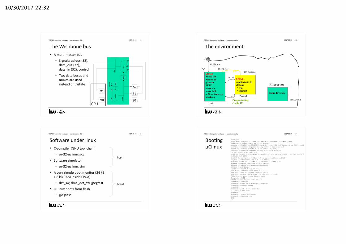
Web server2017-10-30 25TSEA44: Computer hardware – a system on a chip
Lecture info1 Course Intro, FPGA
2 Verilog (lab0)
3 A soft CPU
4 A soft computer (lab1)
5 HW acceleration (lab2), guest lecture from ARM
6 FPGAs
7 Test benches, SV
8 Custom instructions (lab4)
2017-10-30 26TSEA44: Computer hardware – a system on a chip
BooksLilja,Saptnekar: Designing Digital Computer Systems with Verilog, Cambridge University Press
Sutherland et al: SystemVerilog for Design, Springer
Spear: SystemVerilog for Verification, Springer
2017-10-30 27TSEA44: Computer hardware – a system on a chip
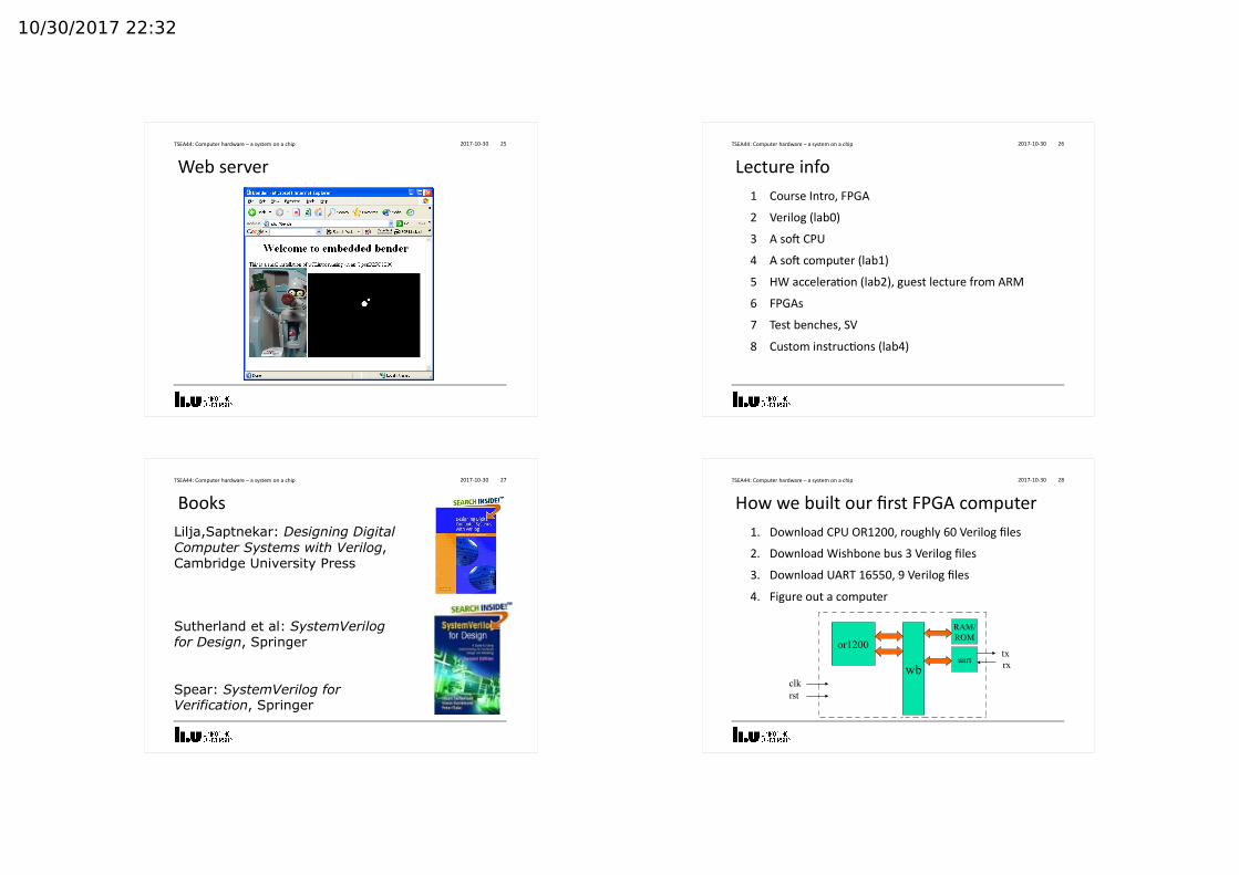
How we built our first FPGA computer1. Download CPU OR1200, roughly 60 Verilog files
2. Download Wishbone bus 3 Verilog files
3. Download UART 16550, 9 Verilog files
4. Figure out a computer
2017-10-30 28TSEA44: Computer hardware – a system on a chip
wb
or1200uart
RAM/ROM
txrx
clkrst
10/30/2017 22:32
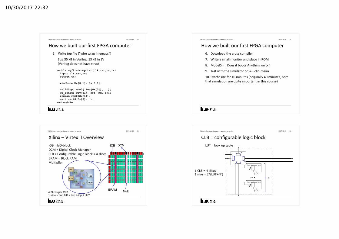
How we built our first FPGA computer5. Write top file (”wire wrap in emacs”)
Size 35 kB in Verilog, 13 kB in SV(Verilog does not have struct)
2017-10-30 29TSEA44: Computer hardware – a system on a chip
module myfirstcomputer(clk,rst,rx,tx) input clk,rst,rx; output tx;
wishbone Mx[0:1], Sx[0:1];
or1200cpu cpu0(.iwb(Mx[0]), … ); wb_conbus wb0(clk, rst, Mx, Sx); romram rom0(Sx[1]); uart uart0(Sx[0], …);end module
How we built our first FPGA computer6. Download the cross compiler
7. Write a small monitor and place in ROM
8. ModelSim. Does it boot? Anything on tx?
9. Test with the simulator or32-uclinux-sim
10. Synthesize for 10 minutes (originally 40 minutes, note that simulation are quite important in this course)
2017-10-30 30TSEA44: Computer hardware – a system on a chip
Xilinx – Virtex II OverviewIOB = I/O-blockDCM = Digital Clock ManagerCLB = Configurable Logic Block = 4 slicesBRAM = Block RAMMultiplier
2017-10-30 31TSEA44: Computer hardware – a system on a chip
IOB DCM
BRAM Mult4 Slices per CLB1 slice = two F/F + two 4-input LUT
CLB = configurable logic blockLUT = look up table
2017-10-30 32TSEA44: Computer hardware – a system on a chip
4
1
look up table 16x1
4
1
look up table 16x1
… 8
1 CLB = 4 slices1 slice = 2*(LUT+FF)
10/30/2017 22:32
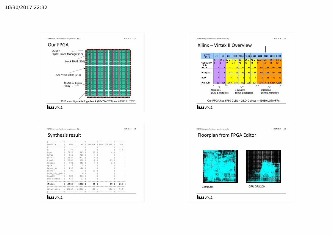
Our FPGA2017-10-30 33TSEA44: Computer hardware – a system on a chip
DCM = Digital Clock Manager (12)
IOB = I/O Block (912)
CLB = configurable logic block (80x72=5760) => 46080 LUT/FF
block RAM (120)
18x18 multiplier(120)
Xilinx – Virtex II Overview
2017-10-30 34TSEA44: Computer hardware – a system on a chip
6 Columns BRAM & Multipliers
4 Columns BRAM & Multipliers
2 Columns BRAM & Multipliers
Our FPGA has 5760 CLBs = 23.040 slices = 46080 LUTs+FFs
Synthesis result2017-10-30 35TSEA44: Computer hardware – a system on a chip
|------------+-------+-------+--------+------------+-------||Module | LUT | FF | RAMB16 | MULT_18x18 | IOB ||------------+-------+-------+--------+------------+-------||/ | 64 | | | | 216 ||cpu | 5029 | 1345 | 12 | 4 | ||dvga | 813 | 755 | 4 | | ||eth3 | 3022 | 2337 | 4 | | ||jpg0 | 2203 | 900 | 2 | 13 | ||leela | 685 | 552 | 4 | 2 | ||pia | 2 | 5 | | | ||pkmc_mc | 218 | 122 | | | ||rom0 | 82 | 3 | 12 | | ||sys_sig_gen | | 6 | | | ||uart2 | 825 | 346 | | | ||wb_conbus | 616 | 11 | | | ||------------+-------+-------+--------+------------+-------+|Total | 13559 | 6382 | 38 | 19 | 216 ||------------+-------+-------+--------+------------+-------+ |Available + 46080 + 46080 + 120 + 120 + 912 ||------------+-------+-------+--------+------------+-------+
Floorplan from FPGA Editor2017-10-30 36TSEA44: Computer hardware – a system on a chip
Computer CPU OR1200
10/30/2017 22:32
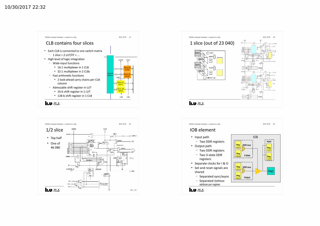
CLB contains four slices● Each CLB is connected to one switch matrix
– 1 slice = 2 LUT/FF + ...● High level of logic integration
– Wide-input functions● 16:1 multiplexer in 1 CLB● 32:1 multiplexer in 2 CLBs
– Fast arithmetic functions● 2 look-ahead carry chains per CLB
column– Adressable shift register in LUT
● 16-b shift register in 1 LUT● 128-b shift register in 1 CLB
2017-10-30 37TSEA44: Computer hardware – a system on a chip
CIN
SwitchMatrix
COUTCOUT
Slice S0X0Y0
Slice S1X0Y1
Slice S2X1Y0
Slice S3X1Y1
CIN
SHIFT
1 slice (out of 23 040)2017-10-30 38TSEA44: Computer hardware – a system on a chip
1/2 slice ● Top half● One of
46 080
2017-10-30 39TSEA44: Computer hardware – a system on a chip
IOB element● Input path
– Two DDR registers● Output path
– Two DDR registers– Two 3-state DDR
registers● Separate clocks for I & O● Set and reset signals are
shared– Separated sync/async– Separated Set/Reset
attribute per register
2017-10-30 40TSEA44: Computer hardware – a system on a chip
Reg
Reg
DDR mux
3-State
OCK1
OCK2
Reg
Reg
DDR mux
Output
OCK1
OCK2
PAD
Reg
Reg
Input
ICK1
ICK2
IOB
10/30/2017 22:32
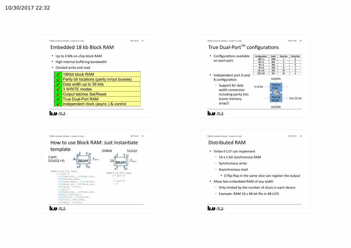
Embedded 18 kb Block RAM● Up to 3 Mb on-chip block RAM● High internal buffering bandwidth● Clocked write and read
2017-10-30 41TSEA44: Computer hardware – a system on a chip
18Kbit block RAMParity bit locations (parity in/out busses)Data width up to 36 bits3 WRITE modesOutput latches Set/ResetTrue Dual-Port RAMIndependent clock (async.) & control
True Dual-PortTM configurations● Configurations available
on each port:
● Independent port A and B configuration.– Support for data
width conversion including parity bits (same memory array!)
2017-10-30 42TSEA44: Computer hardware – a system on a chip
Configuration Depth Data bits Parity bits16K x 1 16Kb 1 08K x 2 8Kb 2 04K x 4 4Kb 4 02K x 9 2Kb 8 1
1K x 18 1Kb 16 2512 x 36 512 32 4
ADDRB
ADDRA
Port A:8 bit
Port B:32 bit
Out 32-bit
In 8-bit
How to use Block RAM: Just Instantiate template
2017-10-30 43TSEA44: Computer hardware – a system on a chip
32
32
9
32
32
9BRAM
8
8
11
32
32
9BRAM
RAMB16_S36_S36 inmem (// port A .CLKA(wb.clk), .SSRA(wb.rst), .ADDRA(bram_addr), .DIA(bram_data), .DIPA(4'h0), .ENA(bram_ce), .WEA(bram_we), .DOA(doa), .DOPA(), // port B .CLKB(wb.clk), .SSRB(wb.rst), .ADDRB({3'h0,rdc}), .DIB(32'h0), .DIPB(4'h0), .ENB(1'b1),.WEB(1'b0), .DOB(dob), .DOPB());
RAMB16_S9_S36 inmem (// port A … // port B … );
2-port 512x32(+4)
2048x8 512x32
Distributed RAM● Virtex-II LUT can implement
– 16 x 1-bit synchronous RAM
– Synchronous write
– Asynchronous read● D flip-flop in the same slice can register the output
● Allow fast embedded RAM of any width
– Only limited by the number of slices in each device
– Example: RAM 16 x 48-bit fits in 48 LUTs
2017-10-30 44TSEA44: Computer hardware – a system on a chip
10/30/2017 22:32
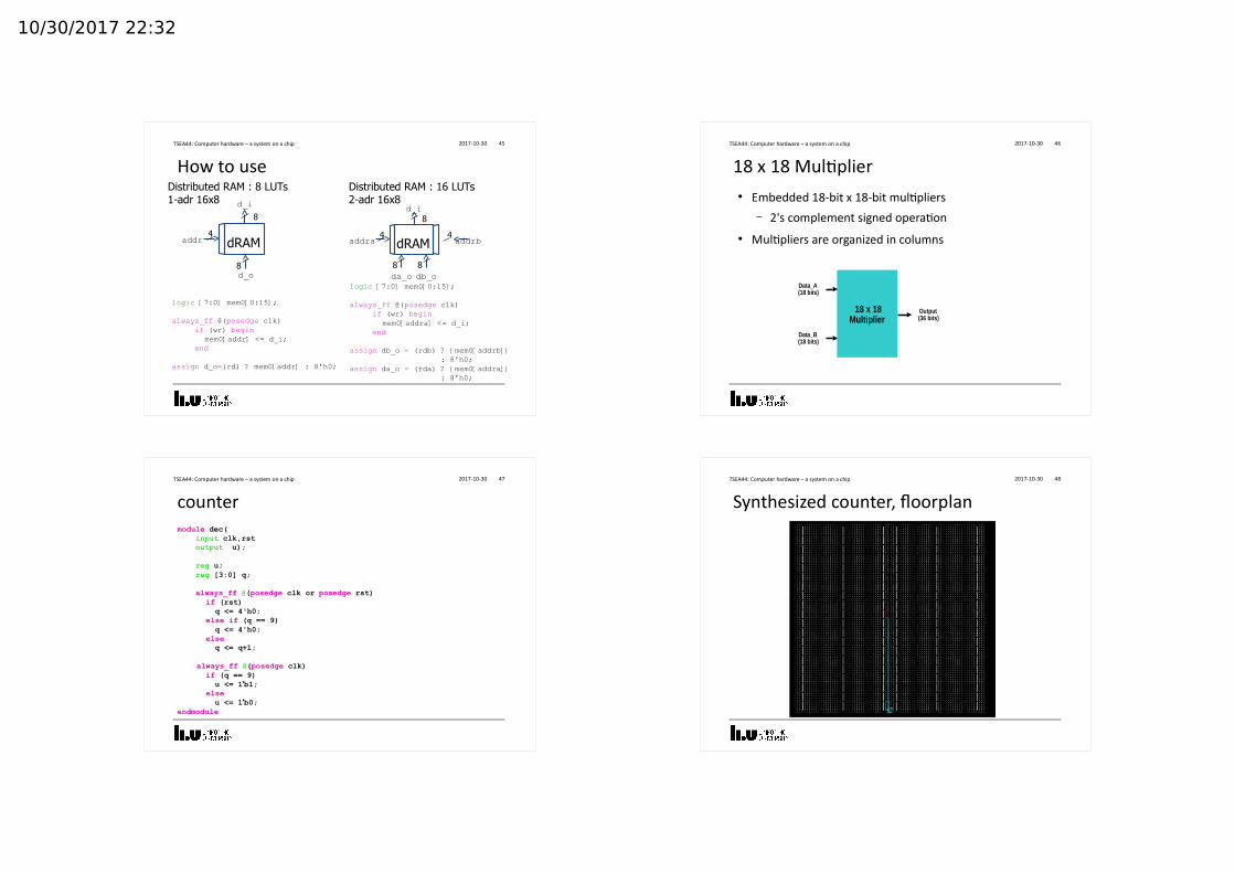
How to use 2017-10-30 45TSEA44: Computer hardware – a system on a chip
8
4
8
dRAMaddr
d_i
d_o
Distributed RAM : 8 LUTs 1-adr 16x8
logic [7:0] mem0[0:15];
always_ff @(posedge clk) if (wr) begin
mem0[addr] <= d_i; end
assign d_o=(rd) ? mem0[addr] : 8'h0;
Distributed RAM : 16 LUTs2-adr 16x8
8
4
8
4dRAM
8
addra addrb
d_i
da_o db_ologic [7:0] mem0[0:15];
always_ff @(posedge clk) if (wr) begin
mem0[addra] <= d_i; end
assign db_o = (rdb) ? {mem0[addrb]} : 8'h0;assign da_o = (rda) ? {mem0[addra]} : 8'h0;
18 x 18 Multiplier● Embedded 18-bit x 18-bit multipliers
– 2's complement signed operation● Multipliers are organized in columns
2017-10-30 46TSEA44: Computer hardware – a system on a chip
18 x 18Multiplier
Output (36 bits)
Data_A (18 bits)
Data_B (18 bits)
countermodule dec( input clk,rst output u);
reg u; reg [3:0] q;
always_ff @(posedge clk or posedge rst) if (rst)
q <= 4'h0; else if (q == 9) q <= 4'h0; else q <= q+1;
always_ff @(posedge clk) if (q == 9)
u <= 1'b1; else u <= 1'b0;
endmodule
2017-10-30 47TSEA44: Computer hardware – a system on a chip
Synthesized counter, floorplan2017-10-30 48TSEA44: Computer hardware – a system on a chip
10/30/2017 22:32

Syntesized counter, detailed floorplan2017-10-30 49TSEA44: Computer hardware – a system on a chip
urst
clk
2 slices
Synthesized counter, logic description2017-10-30 50TSEA44: Computer hardware – a system on a chip
2 slices = 4 LUTs
LUT
q0q1q2q3
LUT
q0q1q2q3
LUT
q0q1q2q3
LUT
q0q0
q1
q2
q3
q0q1q2q3
u+
padu+ u
I/O-buffe
r
0123011 )( qqqqqqq
Hints for lab work● Remember to think hardware!
– Draw block diagrams
– Each block should be simple to translate to verilog● Counters● Registers● Boolean expressions, arithmetic operations● State machines
– Use testbenches and simulate to verify behavor
– Finally test on hardware
2017-10-30 51TSEA44: Computer hardware – a system on a chip
www.liu.se
10/30/2017 22:32