Embed Size (px)
Citation preview
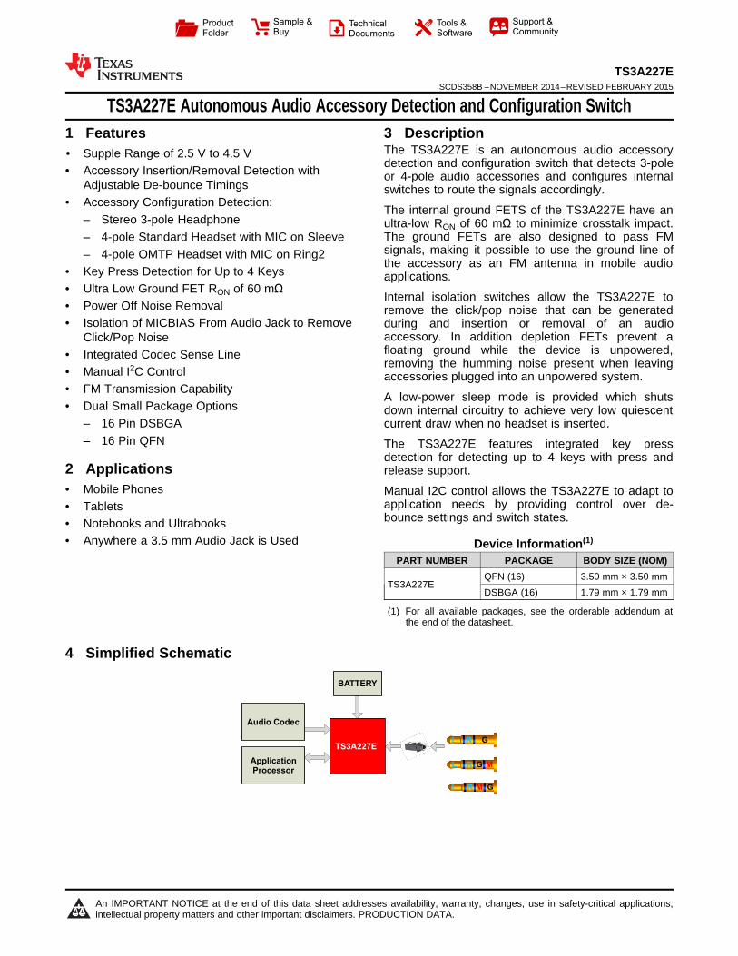
BATTERY
ApplicationProcessor
TS3A227E
Audio Codec
L R G
L R G M
L R GM
Product
Folder
Sample &Buy
Technical
Documents
Tools &
Software
Support &Community
TS3A227ESCDS358B –NOVEMBER 2014–REVISED FEBRUARY 2015
TS3A227E Autonomous Audio Accessory Detection and Configuration Switch1 Features 3 Description
The TS3A227E is an autonomous audio accessory1• Supple Range of 2.5 V to 4.5 V
detection and configuration switch that detects 3-pole• Accessory Insertion/Removal Detection with or 4-pole audio accessories and configures internalAdjustable De-bounce Timings switches to route the signals accordingly.
• Accessory Configuration Detection: The internal ground FETS of the TS3A227E have an– Stereo 3-pole Headphone ultra-low RON of 60 mΩ to minimize crosstalk impact.
The ground FETs are also designed to pass FM– 4-pole Standard Headset with MIC on Sleevesignals, making it possible to use the ground line of– 4-pole OMTP Headset with MIC on Ring2the accessory as an FM antenna in mobile audio
• Key Press Detection for Up to 4 Keys applications.• Ultra Low Ground FET RON of 60 mΩ
Internal isolation switches allow the TS3A227E to• Power Off Noise Removal remove the click/pop noise that can be generated• Isolation of MICBIAS From Audio Jack to Remove during and insertion or removal of an audio
accessory. In addition depletion FETs prevent aClick/Pop Noisefloating ground while the device is unpowered,• Integrated Codec Sense Lineremoving the humming noise present when leaving
• Manual I2C Control accessories plugged into an unpowered system.• FM Transmission Capability
A low-power sleep mode is provided which shuts• Dual Small Package Options down internal circuitry to achieve very low quiescent
– 16 Pin DSBGA current draw when no headset is inserted.– 16 Pin QFN The TS3A227E features integrated key press
detection for detecting up to 4 keys with press and2 Applications release support.• Mobile Phones Manual I2C control allows the TS3A227E to adapt to
application needs by providing control over de-• Tabletsbounce settings and switch states.• Notebooks and Ultrabooks
• Anywhere a 3.5 mm Audio Jack is Used Device Information(1)
PART NUMBER PACKAGE BODY SIZE (NOM)QFN (16) 3.50 mm × 3.50 mm
TS3A227EDSBGA (16) 1.79 mm × 1.79 mm
(1) For all available packages, see the orderable addendum atthe end of the datasheet.
4 Simplified Schematic
1
An IMPORTANT NOTICE at the end of this data sheet addresses availability, warranty, changes, use in safety-critical applications,intellectual property matters and other important disclaimers. PRODUCTION DATA.
TS3A227ESCDS358B –NOVEMBER 2014–REVISED FEBRUARY 2015 www.ti.com
Table of Contents9.2 Functional Block Diagram ....................................... 181 Features .................................................................. 19.3 Feature Description................................................. 192 Applications ........................................................... 19.4 Device Functional Modes........................................ 203 Description ............................................................. 19.5 Register Maps ........................................................ 244 Simplified Schematic............................................. 19.6 Register Field Descriptions ..................................... 245 Revision History..................................................... 2
10 Application and Implementation........................ 336 Pin Configuration and Functions ......................... 310.1 Application Information.......................................... 337 Specifications......................................................... 4 10.2 Typical Application ............................................... 33
7.1 Absolute Maximum Ratings ...................................... 4 11 Power Supply Recommendations ..................... 477.2 ESD Ratings ............................................................ 412 Layout................................................................... 487.3 Recommended Operating Conditions....................... 5
12.1 Layout Guidelines ................................................. 487.4 Thermal Information .................................................. 512.2 Layout Example (QFN) ......................................... 487.5 Electrical Characteristics........................................... 612.3 Layout Example (DSBGA) .................................... 497.6 I2C Interface Timing Characteristics ......................... 8
13 Device and Documentation Support ................. 507.7 Timing Diagrams....................................................... 913.1 Trademarks ........................................................... 507.8 Typical Characteristics ............................................ 1213.2 Electrostatic Discharge Caution............................ 508 Parameter Measurement Information ................ 1213.3 Glossary ................................................................ 509 Detailed Description ............................................ 17
14 Mechanical, Packaging, and Orderable9.1 Overview ................................................................. 17 Information ........................................................... 50
5 Revision History
Changes from Revision A (December 2014) to Revision B Page
• Added DSBGA package to the Thermal Information table. ................................................................................................... 5• Updated SWITCH RESISTANCE for the DSBGA package. ................................................................................................. 6
Changes from Original (July 2014) to Revision A Page
• Initial release of full version document. ................................................................................................................................. 1
2 Submit Documentation Feedback Copyright © 2014–2015, Texas Instruments Incorporated
Product Folder Links: TS3A227E
GND
TIP
GND
SDA
VDD
MIC
P
GNDA
RING2
SLEEVE
SCL
THERMALPAD
16 15 14 13
5 6 7 8
1
2
3
4
12
11
10
9
RIN
G2_S
EN
SE
SLE
EV
E_S
EN
SE
GN
D_S
EN
SE
DE
T_T
RIG
GE
R
MC
_P
RE
SE
NT
INT
4 3 2 1
D
C
B
AVDD
SLEEVE_SENSE
GND
INT
SDA
SCL
GND
TIP
RING2
MICP
RING2_SENSE
MIC_PRESENT
GND_
SENSE
DET_TRIGGER
SLEEVE GNDA
TS3A227Ewww.ti.com SCDS358B –NOVEMBER 2014–REVISED FEBRUARY 2015
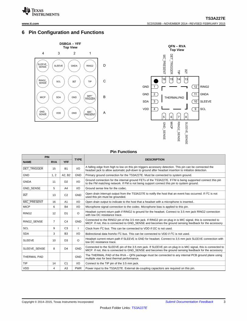
6 Pin Configuration and Functions
DSBGA – YFFQFN – RVATop ViewTop View
Pin FunctionsPIN
TYPE DESCRIPTIONNAME RVA YFF
A falling edge from high to low on this pin triggers accessory detection. This pin can be connected theDET_TRIGGER 15 B1 I/O headset jack to allow automatic pull-down to ground after headset insertion to initialize detection.
GND 1, 2 A2, B2 GND Primary ground connection for the TS3A227E. Must be connected to system ground.
Ground connection for the internal ground FETs of the TS3A227E. If FM is being supported connect this pinGNDA 11 D2 I/O to the FM matching network. If FM is not being support connect this pin to system ground.
GND_SENSE 5 A4 I/O Ground sense line for the codec.
Open drain interrupt output from the TS3A227E to notify the host that an event has occurred. If I2C is notINT 13 C2 GND used this pin must be grounded.
MIC_PRESENT 16 A1 I/O Open drain output to indicate to the host that a headset with a microphone is inserted..
MICP 6 B4 I/O Microphone signal connection to the codec. Microphone bias is applied to this pin.
Headset current return path if RING2 is ground for the headset. Connect to 3.5 mm jack RING2 connectionRING2 12 D1 O with low DC resistance trace.
Connected to the RING2 pin of the 3.5 mm jack. If RING2 pin on plug in is MIC signal, this is connected toRING2_SENSE 7 C4 GND MICP. If not, this is connected to GND_SENSE and becomes the ground sensing feedback for the accessory
SCL 9 C3 I Clock from I2C bus. This can be connected to VDD if I2C is not used.
SDA 3 B3 I/O Bidirectional data from/to I2C bus. This can be connected to VDD if I2C is not used.
Headset current return path if SLEEVE is GND for headset. Connect to 3.5 mm jack SLEEVE connection withSLEEVE 10 D3 O low DC resistance trace.
Connected to the SLEEVE pin of the 3.5 mm jack. If SLEEVE pin on plug in is MIC signal, this is connected toSLEEVE_SENSE 8 D4 GND MICP. If not, this is connected to GND_SENSE and becomes the ground sensing feedback for the accessory
The THERMAL PAD of the RVA – QFN package must be connected to any internal PCB ground plane usingTHERMAL PAD GND multiple vias for best thermal performance.
TIP 14 C1 I/O Connect to the TIP pin of the 3.5 mm jack.
VDD 4 A3 PWR Power input to the TS3A227E. External de-coupling capacitors are required on this pin.
Copyright © 2014–2015, Texas Instruments Incorporated Submit Documentation Feedback 3
Product Folder Links: TS3A227E
TS3A227ESCDS358B –NOVEMBER 2014–REVISED FEBRUARY 2015 www.ti.com
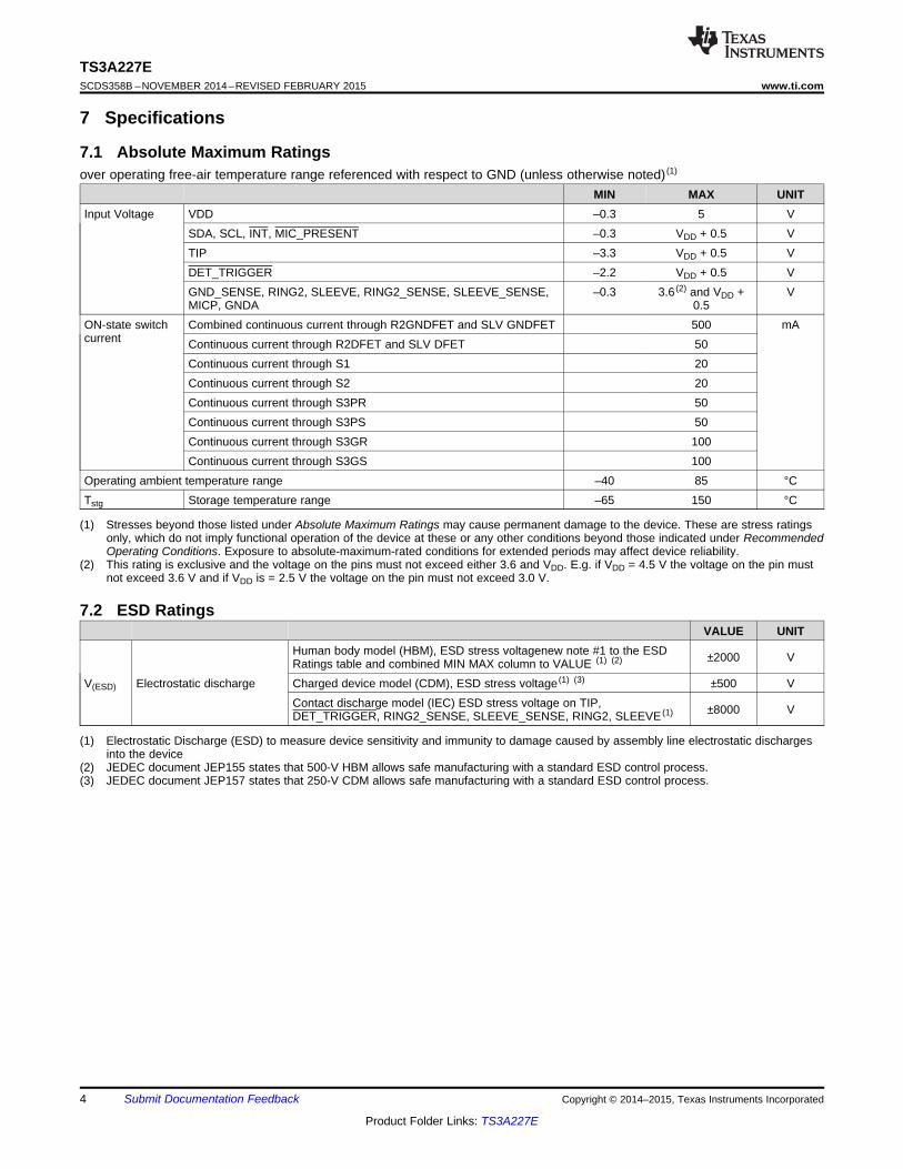
7 Specifications
7.1 Absolute Maximum Ratingsover operating free-air temperature range referenced with respect to GND (unless otherwise noted) (1)
MIN MAX UNITInput Voltage VDD –0.3 5 V
SDA, SCL, INT, MIC_PRESENT –0.3 VDD + 0.5 VTIP –3.3 VDD + 0.5 VDET_TRIGGER –2.2 VDD + 0.5 VGND_SENSE, RING2, SLEEVE, RING2_SENSE, SLEEVE_SENSE, –0.3 3.6 (2) and VDD + VMICP, GNDA 0.5
ON-state switch Combined continuous current through R2GNDFET and SLV GNDFET 500 mAcurrent Continuous current through R2DFET and SLV DFET 50
Continuous current through S1 20Continuous current through S2 20Continuous current through S3PR 50Continuous current through S3PS 50Continuous current through S3GR 100Continuous current through S3GS 100
Operating ambient temperature range –40 85 °CTstg Storage temperature range –65 150 °C
(1) Stresses beyond those listed under Absolute Maximum Ratings may cause permanent damage to the device. These are stress ratingsonly, which do not imply functional operation of the device at these or any other conditions beyond those indicated under RecommendedOperating Conditions. Exposure to absolute-maximum-rated conditions for extended periods may affect device reliability.
(2) This rating is exclusive and the voltage on the pins must not exceed either 3.6 and VDD. E.g. if VDD = 4.5 V the voltage on the pin mustnot exceed 3.6 V and if VDD is = 2.5 V the voltage on the pin must not exceed 3.0 V.
7.2 ESD RatingsVALUE UNIT
Human body model (HBM), ESD stress voltagenew note #1 to the ESD ±2000 VRatings table and combined MIN MAX column to VALUE (1) (2)
V(ESD) Electrostatic discharge Charged device model (CDM), ESD stress voltage (1) (3) ±500 VContact discharge model (IEC) ESD stress voltage on TIP, ±8000 VDET_TRIGGER, RING2_SENSE, SLEEVE_SENSE, RING2, SLEEVE (1)
(1) Electrostatic Discharge (ESD) to measure device sensitivity and immunity to damage caused by assembly line electrostatic dischargesinto the device
(2) JEDEC document JEP155 states that 500-V HBM allows safe manufacturing with a standard ESD control process.(3) JEDEC document JEP157 states that 250-V CDM allows safe manufacturing with a standard ESD control process.
4 Submit Documentation Feedback Copyright © 2014–2015, Texas Instruments Incorporated
Product Folder Links: TS3A227E
TS3A227Ewww.ti.com SCDS358B –NOVEMBER 2014–REVISED FEBRUARY 2015
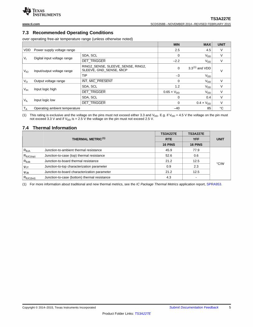
7.3 Recommended Operating Conditionsover operating free-air temperature range (unless otherwise noted)
MIN MAX UNITVDD Power supply voltage range 2.5 4.5 V
SDA, SCL 0 VDD VVI Digital input voltage range
DET_TRIGGER –2.2 VDD VRING2_SENSE, SLEEVE_SENSE, RING2, 0 3.3 (1) and VDDSLEEVE, GND_SENSE, MICPVIO Input/output voltage range VTIP –3 VDD
VO Output voltage range INT, MIC_PRESENT 0 VDD VSDA, SCL 1.2 VDD V
VIH Input logic highDET_TRIGGER 0.65 × VDD VDD VSDA, SCL 0 0.4 V
VIL Input logic lowDET_TRIGGER 0 0.4 × VDD V
TA Operating ambient temperature –40 85 °C
(1) This rating is exclusive and the voltage on the pins must not exceed either 3.3 and VDD. E.g. if VDD = 4.5 V the voltage on the pin mustnot exceed 3.3 V and if VDD is = 2.5 V the voltage on the pin must not exceed 2.5 V.
7.4 Thermal InformationTS3A227E TS3A227E
THERMAL METRIC (1) RTE YFF UNIT16 PINS 16 PINS
RθJA Junction-to-ambient thermal resistance 45.9 77.9RθJC(top) Junction-to-case (top) thermal resistance 52.6 0.6RθJB Junction-to-board thermal resistance 21.2 12.5
°C/WψJT Junction-to-top characterization parameter 0.9 2.3ψJB Junction-to-board characterization parameter 21.2 12.5RθJC(bot) Junction-to-case (bottom) thermal resistance 4.3 -
(1) For more information about traditional and new thermal metrics, see the IC Package Thermal Metrics application report, SPRA953.
Copyright © 2014–2015, Texas Instruments Incorporated Submit Documentation Feedback 5
Product Folder Links: TS3A227E
TS3A227ESCDS358B –NOVEMBER 2014–REVISED FEBRUARY 2015 www.ti.com
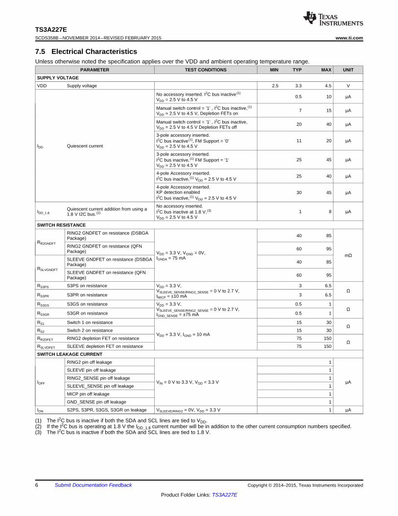
7.5 Electrical CharacteristicsUnless otherwise noted the specification applies over the VDD and ambient operating temperature range.
PARAMETER TEST CONDITIONS MIN TYP MAX UNIT
SUPPLY VOLTAGE
VDD Supply voltage 2.5 3.3 4.5 V
No accessory inserted. I2C bus inactive (1)0.5 10 µAVDD = 2.5 V to 4.5 V
Manual switch control = ’1’ , I2C bus inactive, (1)7 15 µAVDD = 2.5 V to 4.5 V, Depletion FETs on
Manual switch control = ’1’ , I2C bus inactive, 20 40 µAVDD = 2.5 V to 4.5 V Depletion FETs off
3-pole accessory inserted.11 20 µAI2C bus inactive(1), FM Support = ’0’
IDD Quiescent current VDD = 2.5 V to 4.5 V
3-pole accessory inserted.25 45 µAI2C bus inactive, (1) FM Support = ’1’
VDD = 2.5 V to 4.5 V
4-pole Accessory inserted. 25 40 µAI2C bus inactive, (1) VDD = 2.5 V to 4.5 V
4-pole Accessory inserted.KP detection enabled 30 45 µAI2C bus inactive, (1) VDD = 2.5 V to 4.5 V
No accessory inserted.Quiescent current addition from using aIDD_1.8 1 8 µAI2C bus inactive at 1.8 V, (3)1.8 V I2C bus. (2)
VDD = 2.5 V to 4.5 V
SWITCH RESISTANCE
RING2 GNDFET on resistance (DSBGA 40 85Package)RR2GNDFT
RING2 GNDFET on resistance (QFN 60 95Package) VDD = 3.3 V, VGND = 0V, mΩIGNDA = 75 mASLEEVE GNDFET on resistance (DSBGA 40 85Package)RSLVGNDFT
SLEEVE GNDFET on resistance (QFN 60 95Package)
RS3PS S3PS on resistance VDD = 3.3 V, 3 6.5VSLEEVE_SENSE/RING2_SENSE = 0 V to 2.7 V, Ω
RS3PR S3PR on resistance 3 6.5IMICP = ±10 mA
RS3GS S3GS on resistance VDD = 3.3 V, 0.5 1VSLEEVE_SENSE/RING2_SENSE = 0 V to 2.7 V, Ω
RS3GR S3GR on resistance 0.5 1IGND_SENSE = ±75 mA
RS1 Switch 1 on resistance 15 30Ω
RS2 Switch 2 on resistance 15 30VDD = 3.3 V, IGND = 10 mA
RR2DFET RING2 depletion FET on resistance 75 150Ω
RSLVDFET SLEEVE depletion FET on resistance 75 150
SWITCH LEAKAGE CURRENT
RING2 pin off leakage 1
SLEEVE pin off leakage 1
RING2_SENSE pin off leakage 1IOFF VIN = 0 V to 3.3 V, VDD = 3.3 V µA
SLEEVE_SENSE pin off leakage 1
MICP pin off leakage 1
GND_SENSE pin off leakage 1
ION S2PS, S3PR, S3GS, S3GR on leakage VSLEEVE/RING2 = 0V, VDD = 3.3 V 1 µA
(1) The I2C bus is inactive if both the SDA and SCL lines are tied to VDD.(2) If the I2C bus is operating at 1.8 V the IDD_1.8 current number will be in addition to the other current consumption numbers specified.(3) The I2C bus is inactive if both the SDA and SCL lines are tied to 1.8 V.
6 Submit Documentation Feedback Copyright © 2014–2015, Texas Instruments Incorporated
Product Folder Links: TS3A227E
TS3A227Ewww.ti.com SCDS358B –NOVEMBER 2014–REVISED FEBRUARY 2015
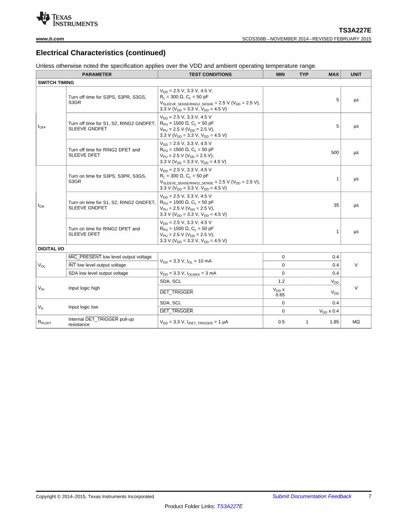
Electrical Characteristics (continued)Unless otherwise noted the specification applies over the VDD and ambient operating temperature range.
PARAMETER TEST CONDITIONS MIN TYP MAX UNIT
SWITCH TIMING
VDD = 2.5 V, 3.3 V, 4.5 V,RL = 300 Ω, CL = 50 pFTurn off time for S3PS, S3PR, S3GS, 5 µsS3GR VSLEEVE_SENSE/RING2_SENSE = 2.5 V (VDD = 2.5 V),3.3 V (VDD = 3.3 V, VDD = 4.5 V)
VDD = 2.5 V, 3.3 V, 4.5 VRPU = 1500 Ω, CL = 50 pFTurn off time for S1, S2, RING2 GNDFET,tOFF 5 µsSLEEVE GNDFET VPU = 2.5 V (VDD = 2.5 V),3.3 V (VDD = 3.3 V, VDD = 4.5 V)
VDD = 2.5 V, 3.3 V, 4.5 VRPU = 1500 Ω, CL = 50 pFTurn off time for RING2 DFET and 500 µsSLEEVE DFET VPU = 2.5 V (VDD = 2.5 V),3.3 V (VDD = 3.3 V, VDD = 4.5 V)
VDD = 2.5 V, 3.3 V, 4.5 VRL = 300 Ω, CL = 50 pFTurn on time for S3PS, S3PR, S3GS, 1 µsS3GR VSLEEVE_SENSE/RING2_SENSE = 2.5 V (VDD = 2.5 V),3.3 V (VDD = 3.3 V, VDD = 4.5 V)
VDD = 2.5 V, 3.3 V, 4.5 VRPU = 1500 Ω, CL = 50 pFTurn on time for S1, S2, RING2 GNDFET,tON 35 µsSLEEVE GNDFET VPU = 2.5 V (VDD = 2.5 V),3.3 V (VDD = 3.3 V, VDD = 4.5 V)
VDD = 2.5 V, 3.3 V, 4.5 VRPU = 1500 Ω, CL = 50 pFTurn on time for RING2 DFET and 1 µsSLEEVE DFET VPU = 2.5 V (VDD = 2.5 V),3.3 V (VDD = 3.3 V, VDD = 4.5 V)
DIGITAL I/O
MIC_PRESENT low level output voltage 0 0.4VDD = 3.3 V, IOL = 10 mA
VOL INT low level output voltage 0 0.4 V
SDA low level output voltage VDD = 3.3 V, IOLMAX = 3 mA 0 0.4
SDA, SCL 1.2 VDD
VIH Input logic high VVDD xDET_TRIGGER VDD0.65
SDA, SCL 0 0.4VIL Input logic low
DET_TRIGGER 0 VDD x 0.4
Internal DET_TRIGGER pull-upRPU/DT VDD = 3.3 V, I/DET_TRIGGER = 1 µA 0.5 1 1.85 MΩresistance
Copyright © 2014–2015, Texas Instruments Incorporated Submit Documentation Feedback 7
Product Folder Links: TS3A227E
TS3A227ESCDS358B –NOVEMBER 2014–REVISED FEBRUARY 2015 www.ti.com
Electrical Characteristics (continued)Unless otherwise noted the specification applies over the VDD and ambient operating temperature range.
PARAMETER TEST CONDITIONS MIN TYP MAX UNIT
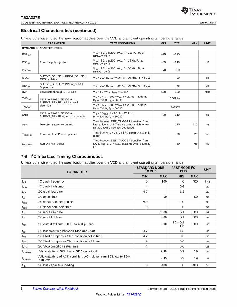
DYNAMIC CHARACTERISTICS
VDD = 3.3 V ± 200 mVPP, f = 217 Hz, RL atPSR217 –95 –120RING2= 50 Ω
VDD = 3.3 V ± 200 mVPP, f = 1 kHz, RL atPSR1k Power supply rejection –85 –110 dBRING2= 50 Ω
VDD = 3.3 V ± 200 mVPP, f = 20 kHz, RL atPSR20k –70 –90RING2= 50 Ω
SLEEVE_SENSE or RING2_SENSE toISOS3 VIN = 200 mVPP, f = 20 Hz – 20 kHz, RL = 50 Ω –90 dBMICP Isolation
SLEEVE_SENSE to RING2_SENSESEPS3 VIN = 200 mVPP, f = 20 Hz – 20 kHz, RL = 50 Ω –75 dBSeparation
BW Bandwidth through GNDFETs VIN = 60 mVPP, IBIAS = 10 mA 120 150 MHz
VIN = 1.5 V + 200 mVPP, f = 20 Hz – 20 kHz,THD200 0.003 %MICP to RING2_SENSE or RS = 600 Ω, RL = 600 ΩSLEEVE_SENSE total harmonic
VIN = 1.5 V + 500 mVPP, f = 20 Hz – 20 kHz,distortionTHD500 0.002%RS = 600 Ω, RL = 600 Ω
VIN = 1 VRMS, f = 20 Hz – 20 kHz,MICP to RING2_SENSE orSNR –90 –110 dBSLEEVE_SENSE signal to noise ratio RS = 600 Ω, RL = 600 Ω
Time between DET_TRIGGER transition fromtDET Detection sequence duration high to low and INT transition from high to low. 175 210 ms
Default 90 ms insertion debounce.
Time from VDD > 2.5 V till I2C communication isTpower-up Power up time Power-up time 20 25 msready
Time between DET_TRIGGER transition fromtREMOVAL Removal wait period low to high and RING2/SLEEVE DFETs turning 50 65 ms
on
7.6 I2C Interface Timing CharacteristicsUnless otherwise noted the specification applies over the VDD and ambient operating temperature range
STANDARD MODE FAST MODE I2C UNITI2C BUS BUSPARAMETERMIN MAX MIN MAX
fscl I2C clock frequency 0 100 0 400 kHztsch I2C clock high time 4 0.6 µstscl I2C clock low time 4.7 1.3 µstsp I2C spike time 50 50 nstsds I2C serial data setup time 250 100 nstsdh I2C serial data hold time 0 0 nsticr I2C input rise time 1000 21 300 nsticf I2C input fall time 300 21 300 ns
20 + 0.1tocf I2C output fall time; 10 pF to 400 pF bus 300 300 µsCbtbuf I2C bus free time between Stop and Start 4.7 1.3 µststs I2C Start or repeater Start condition setup time 4.7 0.6 µststh I2C Start or repeater Start condition hold time 4 0.6 µstsps I2C Stop condition setup time 4 0.6 µstvd(data) Valid data time; SCL low to SDA output valid 3.45 0.3 0.9 µs
Valid data time of ACK condition; ACK signal from SCL low to SDAtvd(ack) 3.45 0.3 0.9 µs(out) lowCb I2C bus capacitive loading 0 400 0 400 pF
8 Submit Documentation Feedback Copyright © 2014–2015, Texas Instruments Incorporated
Product Folder Links: TS3A227E
DET_TRIGGER
INT
Insertion
de-bounce time
(90 ms default )Accessory detection time
(A) (B) (D) (E) (F)
Removal
wait time
MIC_PRESENT High
(C)
TS3A227Ewww.ti.com SCDS358B –NOVEMBER 2014–REVISED FEBRUARY 2015
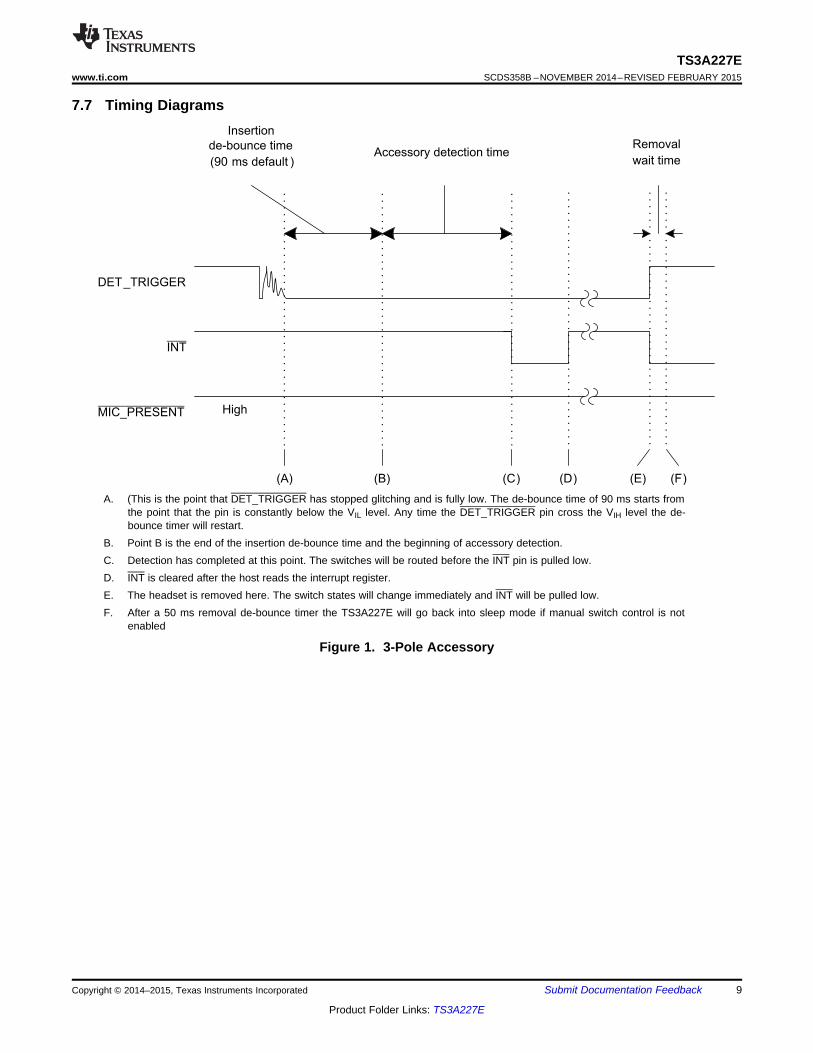
7.7 Timing Diagrams
A. (This is the point that DET_TRIGGER has stopped glitching and is fully low. The de-bounce time of 90 ms starts fromthe point that the pin is constantly below the VIL level. Any time the DET_TRIGGER pin cross the VIH level the de-bounce timer will restart.
B. Point B is the end of the insertion de-bounce time and the beginning of accessory detection.C. Detection has completed at this point. The switches will be routed before the INT pin is pulled low.D. INT is cleared after the host reads the interrupt register.E. The headset is removed here. The switch states will change immediately and INT will be pulled low.F. After a 50 ms removal de-bounce timer the TS3A227E will go back into sleep mode if manual switch control is not
enabled
Figure 1. 3-Pole Accessory
Copyright © 2014–2015, Texas Instruments Incorporated Submit Documentation Feedback 9
Product Folder Links: TS3A227E
DET_TRIGGER
INT
Insertion
de-bounce time
(90 ms default )Accessory detection time
(A) (B) (D) (E) (F)
Removal
wait time
MIC_PRESENT High
(C)
TS3A227ESCDS358B –NOVEMBER 2014–REVISED FEBRUARY 2015 www.ti.com
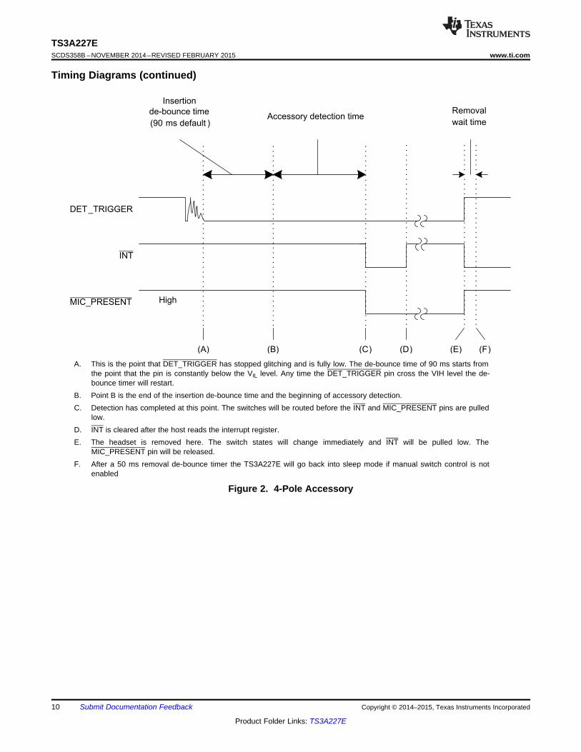
Timing Diagrams (continued)
A. This is the point that DET_TRIGGER has stopped glitching and is fully low. The de-bounce time of 90 ms starts fromthe point that the pin is constantly below the VIL level. Any time the DET_TRIGGER pin cross the VIH level the de-bounce timer will restart.
B. Point B is the end of the insertion de-bounce time and the beginning of accessory detection.C. Detection has completed at this point. The switches will be routed before the INT and MIC_PRESENT pins are pulled
low.D. INT is cleared after the host reads the interrupt register.E. The headset is removed here. The switch states will change immediately and INT will be pulled low. The
MIC_PRESENT pin will be released.F. After a 50 ms removal de-bounce timer the TS3A227E will go back into sleep mode if manual switch control is not
enabled
Figure 2. 4-Pole Accessory
10 Submit Documentation Feedback Copyright © 2014–2015, Texas Instruments Incorporated
Product Folder Links: TS3A227E
DET_TRIGGER
INT
Insertion
de-bounce time
(90 ms default )Accessory detection time
(A) (B) (C) (D) (E) (F)
Removal
wait time
MIC_PRESENT High
TS3A227Ewww.ti.com SCDS358B –NOVEMBER 2014–REVISED FEBRUARY 2015
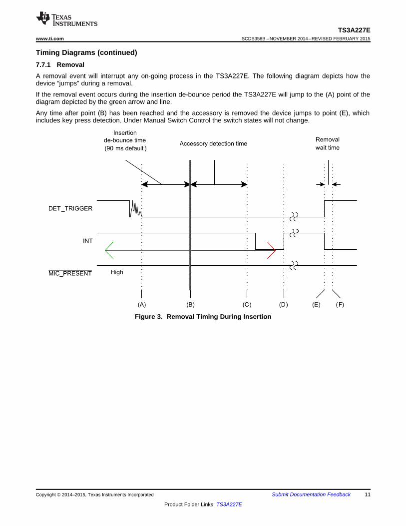
Timing Diagrams (continued)7.7.1 RemovalA removal event will interrupt any on-going process in the TS3A227E. The following diagram depicts how thedevice “jumps” during a removal.
If the removal event occurs during the insertion de-bounce period the TS3A227E will jump to the (A) point of thediagram depicted by the green arrow and line.
Any time after point (B) has been reached and the accessory is removed the device jumps to point (E), whichincludes key press detection. Under Manual Switch Control the switch states will not change.
Figure 3. Removal Timing During Insertion
Copyright © 2014–2015, Texas Instruments Incorporated Submit Documentation Feedback 11
Product Folder Links: TS3A227E
IGNDR2/SLV DFET
VSLEEVE/RING2
Channel ON
RON = VSLEEVE/RING2 / IGND
IGNDAR2/SLV GNDFET
VSLEEVE/RING2
Channel ON
RON = VSLEEVE/RING2 / IGNDA
Frequency (Hz)
THD
(%)
10 2030 50 100 200 5001000 10000 1000000
0.0005
0.001
0.0015
0.002
0.0025
0.003
0.0035
D001
200 mVpp500 mVpp
TS3A227ESCDS358B –NOVEMBER 2014–REVISED FEBRUARY 2015 www.ti.com
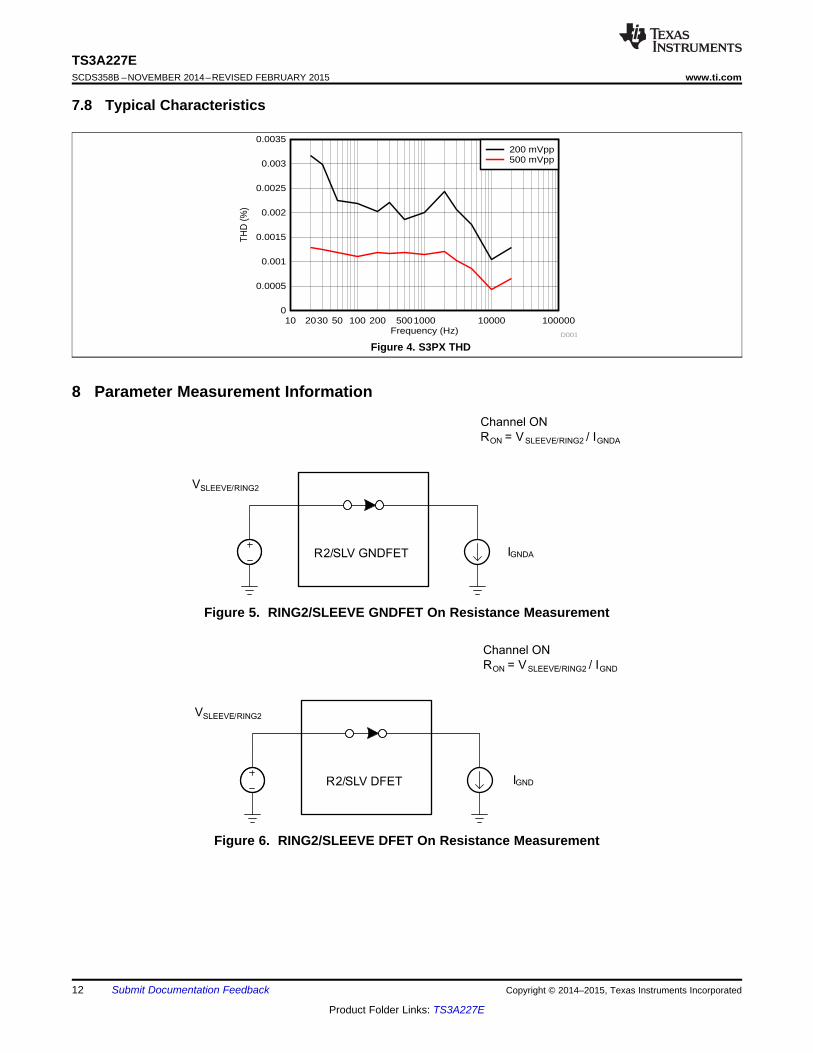
7.8 Typical Characteristics
Figure 4. S3PX THD
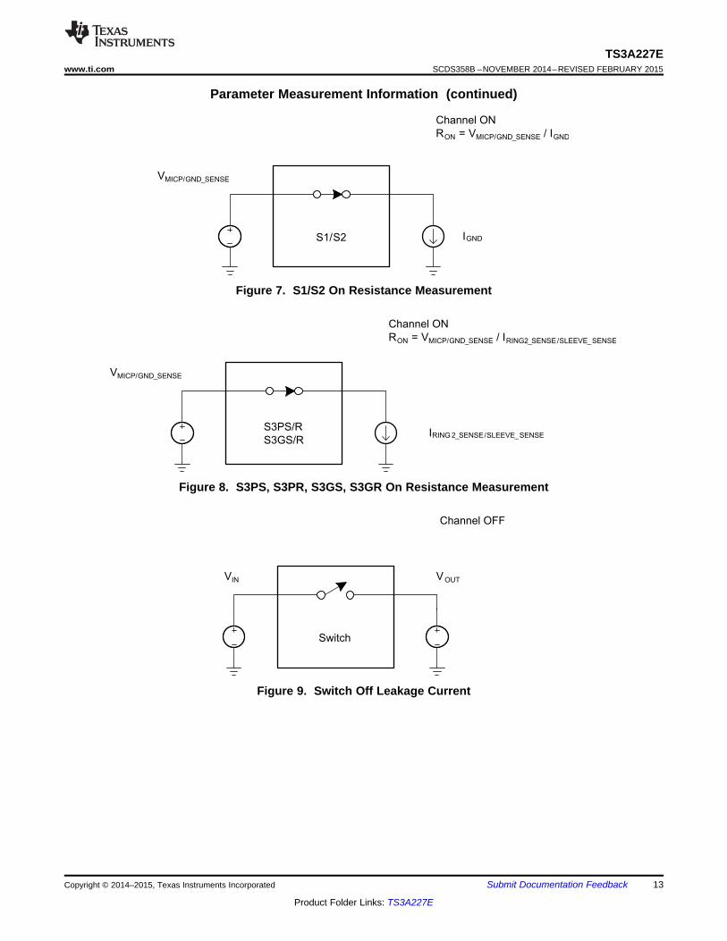
8 Parameter Measurement Information
Figure 5. RING2/SLEEVE GNDFET On Resistance Measurement
Figure 6. RING2/SLEEVE DFET On Resistance Measurement
12 Submit Documentation Feedback Copyright © 2014–2015, Texas Instruments Incorporated
Product Folder Links: TS3A227E
VOUT
Switch
VIN
Channel OFF
IRING 2_SENSE/SLEEVE_SENSES3PS/R
S3GS/R
VMICP/GND_SENSE
Channel ON
RON = VMICP/GND_SENSE / IRING2_SENSE/SLEEVE_SENSE
IGNDS1/S2
VMICP/GND_SENSE
Channel ON
RON = VMICP/GND_SENSE / IGND
TS3A227Ewww.ti.com SCDS358B –NOVEMBER 2014–REVISED FEBRUARY 2015
Parameter Measurement Information (continued)
Figure 7. S1/S2 On Resistance Measurement
Figure 8. S3PS, S3PR, S3GS, S3GR On Resistance Measurement
Figure 9. Switch Off Leakage Current
Copyright © 2014–2015, Texas Instruments Incorporated Submit Documentation Feedback 13
Product Folder Links: TS3A227E
Switch
Network Analyzer
Source
Signal
50 Ω
50 Ω
Channel Off
VMICP/GND_SENSE
VSLEEVE_SENSE/RING2_SENSE
50 Ω
Switch
Channel ON
VDD
3.3 V ± 200 mVPP
Reference
Test
Source Generator
Source
Signal
50 Ω
VOUT
Switch
Channel ON
ILeakage
TS3A227ESCDS358B –NOVEMBER 2014–REVISED FEBRUARY 2015 www.ti.com
Parameter Measurement Information (continued)
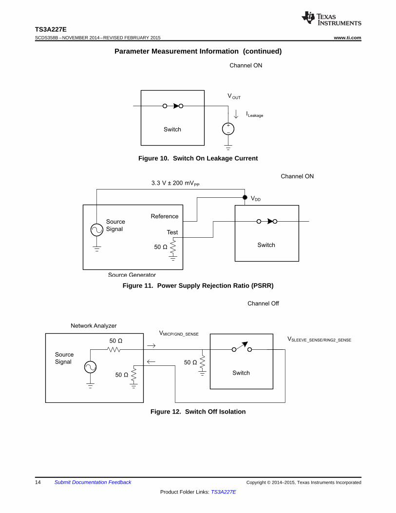
Figure 10. Switch On Leakage Current
Figure 11. Power Supply Rejection Ratio (PSRR)
Figure 12. Switch Off Isolation
14 Submit Documentation Feedback Copyright © 2014–2015, Texas Instruments Incorporated
Product Folder Links: TS3A227E
Audio Analyzer
Source
Signal
600 Ω
600 Ω VMICP VSLEEVE_SENSE/RING2_SENSE
Switch
Network Analyzer
Source
Signal
50 Ω
50 Ω VMICP VSLEEVE_SENSE
50 Ω
50 ΩVGND_SENSE VRING2_SENSE
Switches
TS3A227Ewww.ti.com SCDS358B –NOVEMBER 2014–REVISED FEBRUARY 2015
Parameter Measurement Information (continued)
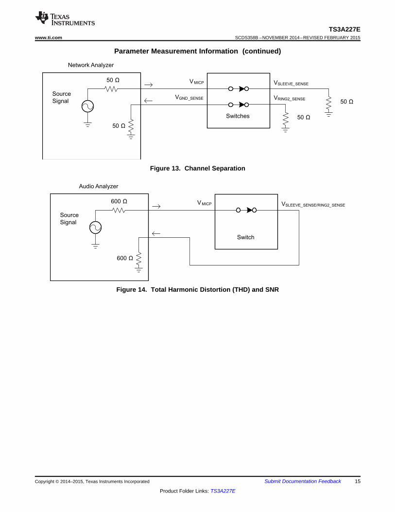
Figure 13. Channel Separation
Figure 14. Total Harmonic Distortion (THD) and SNR
Copyright © 2014–2015, Texas Instruments Incorporated Submit Documentation Feedback 15
Product Folder Links: TS3A227E
Digital
Core
SDA
SCL
RPU
CL
VPU
VTEST
VTEST
SCL
VTEST
70
%
30
%
tOFF
tON
VTEST
SCL
VTEST
90
%
10
%
tON
tOFF
VMICP/GND_SENSE
Digital
Core
SDA
SCL
RL CL
VTEST
TS3A227ESCDS358B –NOVEMBER 2014–REVISED FEBRUARY 2015 www.ti.com
Parameter Measurement Information (continued)
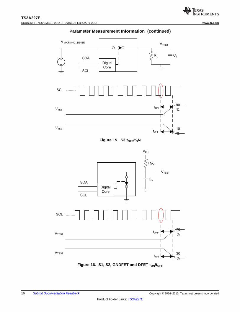
Figure 15. S3 tOFF/tON
Figure 16. S1, S2, GNDFET and DFET tON/tOFF
16 Submit Documentation Feedback Copyright © 2014–2015, Texas Instruments Incorporated
Product Folder Links: TS3A227E
TS3A227Ewww.ti.com SCDS358B –NOVEMBER 2014–REVISED FEBRUARY 2015
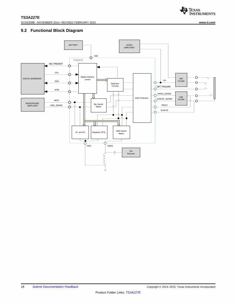
9 Detailed Description
9.1 OverviewThe TS3A227E is an autonomous audio accessory switch with adjustable de-bounce settings, ultra-low RONground FETs, depletion FETs and manual I2C control.
The detection sequence is initiated via the external DET_TRIGGER pin or via I2C command. The deviceincorporates internal de-bounce timings that remove the need for external RC circuits, reducing cost and overallPCB footprint. Additionally all switches of the TS3A227E and the internal de-bounce timings can be controlledthrough I2C.
Before an insertion, TS3A227E isolates the MICBIAS voltage output from the audio jack to remove click/popnoise that can be created during an insertion event. In addition the device also includes depletion FETs toground the accessory SLEEVE and RING2 pins when VDD is not powered. This removes the humming noisethat can be created when plugging an accessory into and unpowered system.
The TS3A227E detects the presence and configuration of the microphone in an attached headset upon insertion.Upon detection of a microphone the TS3A227E automatically connects a system analog microphone pin (MICP)to the appropriate audio jack connection. The device also automatically routes the device GNDA pin to theheadset ground. After a 4-pole headset insertion the host can enable the Key Press detection feature of theTS3A227E.
The device also features an ultra-low power sleep mode to conserve battery life when an accessory is notinserted.
For FM transmission the ground FETs of the device can be used as an FM transmission path by placing the FMreceiver and matching network on the GNDA pin. The FM support bit must be set to ‘1’ through I2C for FMtransmission to pass.
Copyright © 2014–2015, Texas Instruments Incorporated Submit Documentation Feedback 17
Product Folder Links: TS3A227E
BATTERY
DIGITAL BASEBAND
MIC_PRESENT
SCL
SDA
INTB
VDD
MICROPHONE
AMPLIFIER
EMI
FILTER
EMI
FILTER
RING2_SENSE
SLEEVE_SENSE
TIP
DET_TRIGGER
RING2
SLEEVE
MICP
GND_SENSE
AUDIO
AMPLIFIER
Mic Switch
Matrix
ESD Protection
Depletion FETsGND Switch
Matrix
TS3A227E
Detection
Circuitry
Digital interface
control
GND GNDA
FM
Receiver
S1 and S2
TS3A227ESCDS358B –NOVEMBER 2014–REVISED FEBRUARY 2015 www.ti.com
9.2 Functional Block Diagram
18 Submit Documentation Feedback Copyright © 2014–2015, Texas Instruments Incorporated
Product Folder Links: TS3A227E
R M GL
16-2 kΩ
16-2 kΩ
600-4kΩ
OMTP
4-pole TRRS
Tip Ring1 SleeveRing2
R G ML
16-2 kΩ
16-2 kΩ
600-4kΩ
Standard
Tip Ring Sleeve
3-pole TRS
R GL
16-2 kΩ
16-2 kΩ
TRS
TS3A227Ewww.ti.com SCDS358B –NOVEMBER 2014–REVISED FEBRUARY 2015
9.3 Feature Description
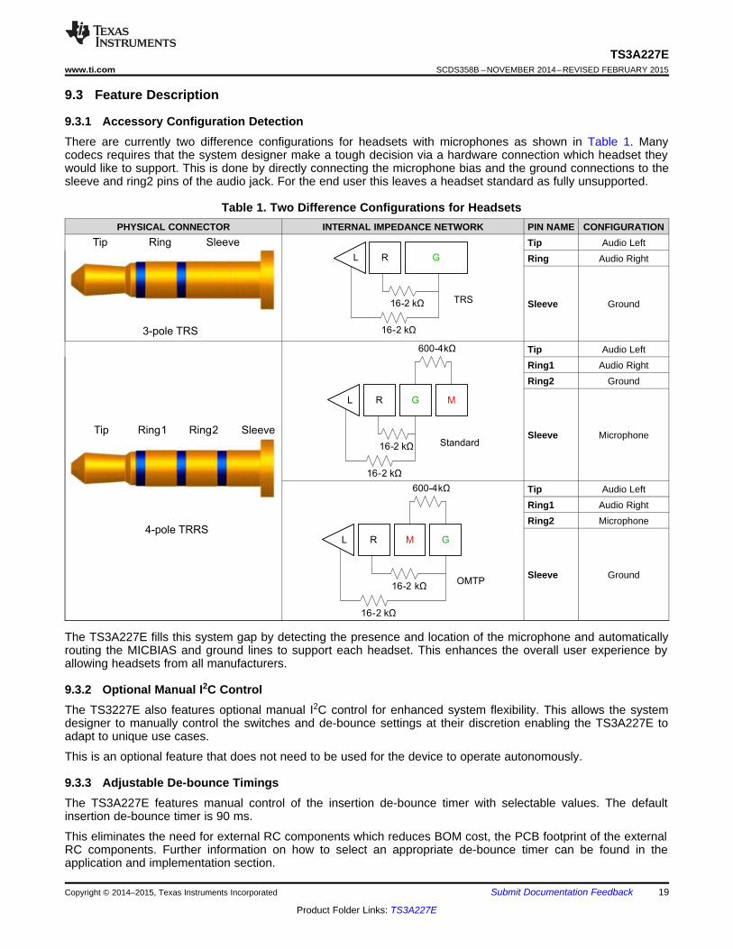
9.3.1 Accessory Configuration DetectionThere are currently two difference configurations for headsets with microphones as shown in Table 1. Manycodecs requires that the system designer make a tough decision via a hardware connection which headset theywould like to support. This is done by directly connecting the microphone bias and the ground connections to thesleeve and ring2 pins of the audio jack. For the end user this leaves a headset standard as fully unsupported.
Table 1. Two Difference Configurations for HeadsetsPHYSICAL CONNECTOR INTERNAL IMPEDANCE NETWORK PIN NAME CONFIGURATION
Tip Audio LeftRing Audio Right
Sleeve Ground
Tip Audio LeftRing1 Audio RightRing2 Ground
Sleeve Microphone
Tip Audio LeftRing1 Audio RightRing2 Microphone
Sleeve Ground
The TS3A227E fills this system gap by detecting the presence and location of the microphone and automaticallyrouting the MICBIAS and ground lines to support each headset. This enhances the overall user experience byallowing headsets from all manufacturers.
9.3.2 Optional Manual I2C ControlThe TS3227E also features optional manual I2C control for enhanced system flexibility. This allows the systemdesigner to manually control the switches and de-bounce settings at their discretion enabling the TS3A227E toadapt to unique use cases.
This is an optional feature that does not need to be used for the device to operate autonomously.
9.3.3 Adjustable De-bounce TimingsThe TS3A227E features manual control of the insertion de-bounce timer with selectable values. The defaultinsertion de-bounce timer is 90 ms.
This eliminates the need for external RC components which reduces BOM cost, the PCB footprint of the externalRC components. Further information on how to select an appropriate de-bounce timer can be found in theapplication and implementation section.
Copyright © 2014–2015, Texas Instruments Incorporated Submit Documentation Feedback 19
Product Folder Links: TS3A227E
TS3A227ESCDS358B –NOVEMBER 2014–REVISED FEBRUARY 2015 www.ti.com
9.3.4 Key Press DetectionAfter a headset is inserted, the host can enable Key Press detection through the I2C registers. This will configurethe TS3A227E to detect up to 4 different keys and report when the key is pressed and released.
9.3.5 Click Pop Noise ReductionDuring an accessory insertion and removal event the TS3A227E use special techniques to remove the click/popnoise that can occur with a traditional implementation creating a better user experience.
9.3.6 Power off Noise RemovalIn a system that intends to support both headset types, the end user can place the system into sleep mode andleave a headset/speaker plugged into the audio jack. If the audio jack switch is turned off to conserve power inthe sleep mode this would typically mean the headset/speaker ground would not be connected because there isno power to turn on the ground FETs. This creates an audible humming noise at the speaker/headset output thatcan be discomforting to listen to.
By utilizing always on depletion FETs this issue can be removed and the headset/speaker can be connected toground even with the device unpowered.
9.3.7 Sleep ModeThe TS3A227E will automatically enter a low power sleep when no accessory is inserted and manual switchcontrol is not enabled. After an accessory is inserted the device will wake, run detection, and configure theswitches as necessary.
9.3.8 Codec Sense LineIn the complex systems of today, there is an increasing amount of ICs on any given board. The issue this createsis that a codec can be far away from the audio jack and there is a potential difference between the grounding ofthe codec and the grounding of the headset.
By incorporating a ground sense line into the TS3A227E the codec can compensate for this offset and create ahigher quality audio experience.
9.3.9 FM SupportFM can be picked up using the headset ground line and passed through the ground FETs of the TS3A227E. Byhaving a bandwidth of 200 MHz the full FM band can be passed through these FETs to a FM matching networkand the FM receiver.
9.4 Device Functional Modes
9.4.1 Sleep ModeThe device will realize a sleep mode of 1 µA if the following are true:• No accessory is inserted• Manual Switch Control = ‘0’
The TS3A227E will respond to I2C communication and insertion events while in sleep mode. The user can setthe de-bounce settings and device configuration as desired while in the sleep mode. If the user sets the ManualSwitch Control bit to ‘1’ the device will turn on all blocks and come out of sleep mode.
If there is no accessory inserted and the users exits manual switch control, the switches will revert to the no-insertion state and all unnecessary blocks of the TS3A227E will turn off and enter the sleep mode.
20 Submit Documentation Feedback Copyright © 2014–2015, Texas Instruments Incorporated
Product Folder Links: TS3A227E
TS3A227Ewww.ti.com SCDS358B –NOVEMBER 2014–REVISED FEBRUARY 2015
Device Functional Modes (continued)9.4.2 Manual Switch ControlThe TS3A227E supports manual switch control that can be utilized by setting Bit6 of the Device Settings 1register to ‘1’.
Key operational characteristics of manual switch control are below.1. Enabling the manual switch control does not disable automatic insertion and accessory type detection.2. Manual Switch Control is blocked during accessory type detection which includes an automatic detection
sequence or a manual SW triggered detection sequence. Any changes to the switch control registers, orsetting the device to manual switch control will not update the switches until after the accessory typedetection has completed.
3. Manual Switch Control is also blocked during de-bounce periods.4. Excluding items 2 and 3 above, immediately after the system enables manual switch control the switch states
will change to reflect the switch control registers. It is advised to set the desired state of the switches beforeenabling manual switch control.
5. Turning off the depletion FETs of the device will result in increased power consumption as defined in theelectrical characteristics table.
6. Immediately upon setting Manual Switch Control = ‘0’ the device will automatically configure the switches tothe latest detection state. If an accessory is inserted but the TS3A227E has not run detection due toAuto_Det_EN = ‘0’, the switch status will revert to the no insertion state.
7. The device cannot be in sleep mode and utilize manual switch control at the same time.
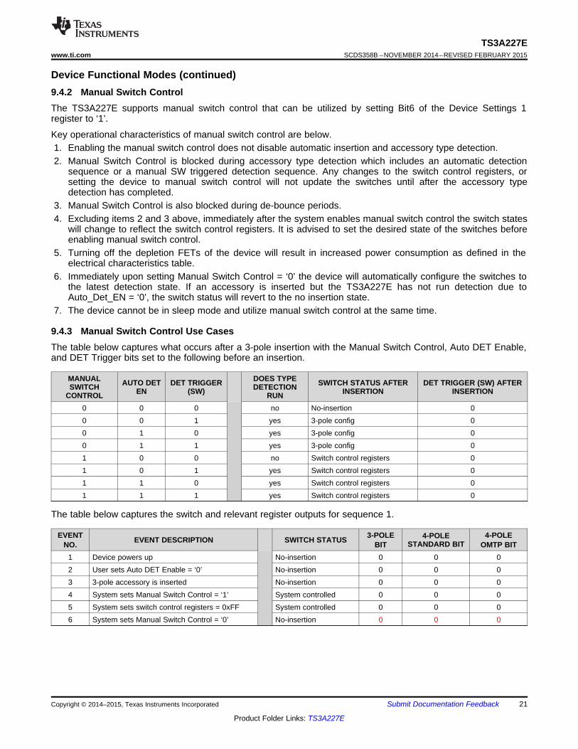
9.4.3 Manual Switch Control Use CasesThe table below captures what occurs after a 3-pole insertion with the Manual Switch Control, Auto DET Enable,and DET Trigger bits set to the following before an insertion.
MANUAL DOES TYPEAUTO DET DET TRIGGER SWITCH STATUS AFTER DET TRIGGER (SW) AFTERSWITCH DETECTIONEN (SW) INSERTION INSERTIONCONTROL RUN0 0 0 no No-insertion 00 0 1 yes 3-pole config 00 1 0 yes 3-pole config 00 1 1 yes 3-pole config 01 0 0 no Switch control registers 01 0 1 yes Switch control registers 01 1 0 yes Switch control registers 01 1 1 yes Switch control registers 0
The table below captures the switch and relevant register outputs for sequence 1.
EVENT 3-POLE 4-POLE4-POLEEVENT DESCRIPTION SWITCH STATUS STANDARD BITNO. BIT OMTP BIT1 Device powers up No-insertion 0 0 02 User sets Auto DET Enable = ‘0’ No-insertion 0 0 03 3-pole accessory is inserted No-insertion 0 0 04 System sets Manual Switch Control = ‘1’ System controlled 0 0 05 System sets switch control registers = 0xFF System controlled 0 0 06 System sets Manual Switch Control = ‘0’ No-insertion 0 0 0
Copyright © 2014–2015, Texas Instruments Incorporated Submit Documentation Feedback 21
Product Folder Links: TS3A227E
TS3A227ESCDS358B –NOVEMBER 2014–REVISED FEBRUARY 2015 www.ti.com
In sequence 1 at event 3 the switch status does not change because the system set the Auto DET Enable = ‘0’.When the accessory is inserted we will not run detection and not change the switches because of this.
At event 6 the system turns off manual switch control, the switch state reverts back to the No-insertion statebecause the TS3A227E has not ran detection.
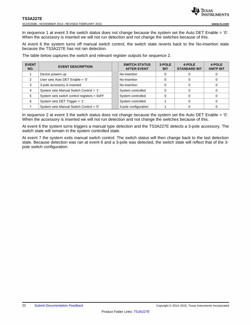
The table below captures the switch and relevant register outputs for sequence 2.
EVENT SWITCH STATUS 3-POLE 4-POLE 4-POLEEVENT DESCRIPTIONNO. AFTER EVENT BIT STANDARD BIT OMTP BIT1 Device powers up No-insertion 0 0 02 User sets Auto DET Enable = ‘0’ No-insertion 0 0 03 3-pole accessory is inserted No-insertion 0 0 04 System sets Manual Switch Control = ‘1’ System controlled 0 0 05 System sets switch control registers = 0xFF System controlled 0 0 06 System sets DET Trigger = ‘1’ System controlled 1 0 07 System sets Manual Switch Control = '0' 3-pole configuration 1 0 0
In sequence 2 at event 3 the switch status does not change because the system set the Auto DET Enable = ‘0’.When the accessory is inserted we will not run detection and not change the switches because of this.
At event 6 the system turns triggers a manual type detection and the TS3A227E detects a 3-pole accessory. Theswitch state will remain in the system controlled state.
At event 7 the system exits manual switch control. The switch status will then change back to the last detectionstate. Because detection was ran at event 6 and a 3-pole was detected, the switch state will reflect that of the 3-pole switch configuration.
22 Submit Documentation Feedback Copyright © 2014–2015, Texas Instruments Incorporated
Product Folder Links: TS3A227E
TS3A227E
MICP
GND_SENSE
S3PR
SLEEVE
S3PS
S3GS
S3GR
S1 S2RING2
GNDFET
SLEEVE
GNDFET
RING2
DFET
SLEEVE
DFET
RING2
SLEEVE_SENSE
RING 2_SENSE
GND GNDGNDA
Audio Jack
L R G M
FM
Receiver
TS3A227Ewww.ti.com SCDS358B –NOVEMBER 2014–REVISED FEBRUARY 2015
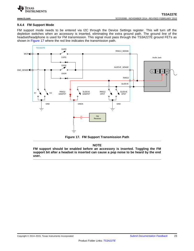
9.4.4 FM Support ModeFM support mode needs to be entered via I2C through the Device Settings register. This will turn off thedepletion switches when an accessory is inserted, eliminating the extra ground path. The ground line of theheadset/headphone is used for FM transmission. This signal must pass through the TS3A227E ground FETs asshown in Figure 17 where the red line indicates the transmission path.
Figure 17. FM Support Transmission Path
NOTEFM support should be enabled before an accessory is inserted. Toggling the FMsupport bit after a headset is inserted can cause a pop noise to be heard by the enduser.
Copyright © 2014–2015, Texas Instruments Incorporated Submit Documentation Feedback 23
Product Folder Links: TS3A227E
TS3A227ESCDS358B –NOVEMBER 2014–REVISED FEBRUARY 2015 www.ti.com
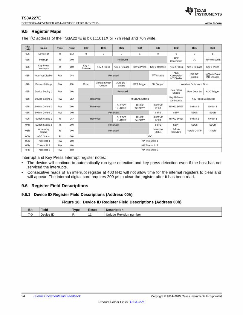
9.5 Register MapsThe I2C address of the TS3A227E is b’0111011X or 77h read and 76h write.
Addr Name Type Reset Bit7 Bit6 Bit5 Bit4 Bit3 Bit2 Bit1 Bit0(xxh)
00h Device ID R 11h 0 0 0 1 0 0 0 1
ADC01h Interrupt R 00h Reserved DC Ins/Rem EventConversion
Key Press Key 402h R 00h Key 4 Press Key 3 Release Key 3 Press Key 2 Release Key 2 Press Key 1 Release Key 1 PressInterrupts Release
ADC DC INT Ins/Rem Event03h Interrupt Disable R/W 08h Reserved INT Disable Conversion Disable INT DisableINT Disable
Manual Switch Auto DET04h Device Settings R/W 23h Reset DET Trigger FM Support Insertion De-bounce TimeControl Enable
Key Press05h Device Setting 1 R/W 00h Reserved Raw Data En ADC TriggerEnable
Key Release06h Device Setting 2 R/W 0Eh Reserved MICBIAS Setting Key Press De-bounce
De-bounce
RING2SLEEVE SLEEVE07h Switch Control 1 R/W 00h Reserved RING2 DFET Switch 2 Switch 1GNDFET DFETGNDFET
08h Switch Control 2 R/W 00h Reserved S3PS S3PR S3GS S3GR
RING2SLEEVE SLEEVE09h Switch Status 1 R 0Ch Reserved RING2 DFET Switch 2 Switch 1GNDFET DFETGNDFET
0Ah Switch Status 2 R 00h Reserved S3PS S3PR S3GS S3GR
Accessory Insertion 4-Pole0Bh R 00h Reserved 4-pole OMTP 3-poleStatus Status Standard
0Ch ADC Output R 00h ADC
0Dh Threshold 1 R/W 20h KP Threshold 1
0Eh Threshold 2 R/W 40h KP Threshold 2
0Fh Threshold 3 R/W 68h KP Threshold 3
Interrupt and Key Press Interrupt register notes:• The device will continue to automatically run type detection and key press detection even if the host has not
serviced the interrupts.• Consecutive reads of an interrupt register at 400 kHz will not allow time for the internal registers to clear and
will appear. The internal digital core requires 200 µs to clear the register after it has been read.
9.6 Register Field Descriptions
9.6.1 Device ID Register Field Descriptions (Address 00h)
Figure 18. Device ID Register Field Descriptions (Address 00h)
Bit Field Type Reset Description7-0 Device ID R 11h Unique Revision number
24 Submit Documentation Feedback Copyright © 2014–2015, Texas Instruments Incorporated
Product Folder Links: TS3A227E
TS3A227Ewww.ti.com SCDS358B –NOVEMBER 2014–REVISED FEBRUARY 2015
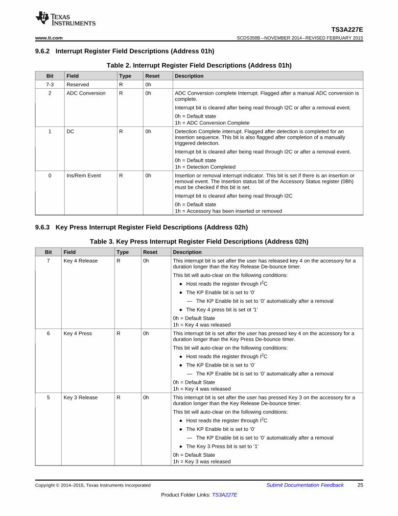
9.6.2 Interrupt Register Field Descriptions (Address 01h)
Table 2. Interrupt Register Field Descriptions (Address 01h)Bit Field Type Reset Description7-3 Reserved R 0h2 ADC Conversion R 0h ADC Conversion complete Interrupt. Flagged after a manual ADC conversion is
complete.Interrupt bit is cleared after being read through I2C or after a removal event.0h = Default state1h = ADC Conversion Complete
1 DC R 0h Detection Complete interrupt. Flagged after detection is completed for aninsertion sequence. This bit is also flagged after completion of a manuallytriggered detection.Interrupt bit is cleared after being read through I2C or after a removal event.0h = Default state1h = Detection Completed
0 Ins/Rem Event R 0h Insertion or removal interrupt indicator. This bit is set if there is an insertion orremoval event. The Insertion status bit of the Accessory Status register (0Bh)must be checked if this bit is set.Interrupt bit is cleared after being read through I2C0h = Default state1h = Accessory has been inserted or removed
9.6.3 Key Press Interrupt Register Field Descriptions (Address 02h)
Table 3. Key Press Interrupt Register Field Descriptions (Address 02h)Bit Field Type Reset Description7 Key 4 Release R 0h This interrupt bit is set after the user has released key 4 on the accessory for a
duration longer than the Key Release De-bounce timer.This bit will auto-clear on the following conditions:
● Host reads the register through I2C● The KP Enable bit is set to ‘0’
— The KP Enable bit is set to ‘0’ automatically after a removal● The Key 4 press bit is set ot '1'
0h = Default State1h = Key 4 was released
6 Key 4 Press R 0h This interrupt bit is set after the user has pressed key 4 on the accessory for aduration longer than the Key Press De-bounce timer.This bit will auto-clear on the following conditions:
● Host reads the register through I2C● The KP Enable bit is set to ‘0’
— The KP Enable bit is set to ‘0’ automatically after a removal0h = Default State1h = Key 4 was released
5 Key 3 Release R 0h This interrupt bit is set after the user has pressed Key 3 on the accessory for aduration longer than the Key Release De-bounce timer.This bit will auto-clear on the following conditions:
● Host reads the register through I2C● The KP Enable bit is set to ‘0’
— The KP Enable bit is set to ‘0’ automatically after a removal● The Key 3 Press bit is set to ‘1’
0h = Default State1h = Key 3 was released
Copyright © 2014–2015, Texas Instruments Incorporated Submit Documentation Feedback 25
Product Folder Links: TS3A227E
TS3A227ESCDS358B –NOVEMBER 2014–REVISED FEBRUARY 2015 www.ti.com
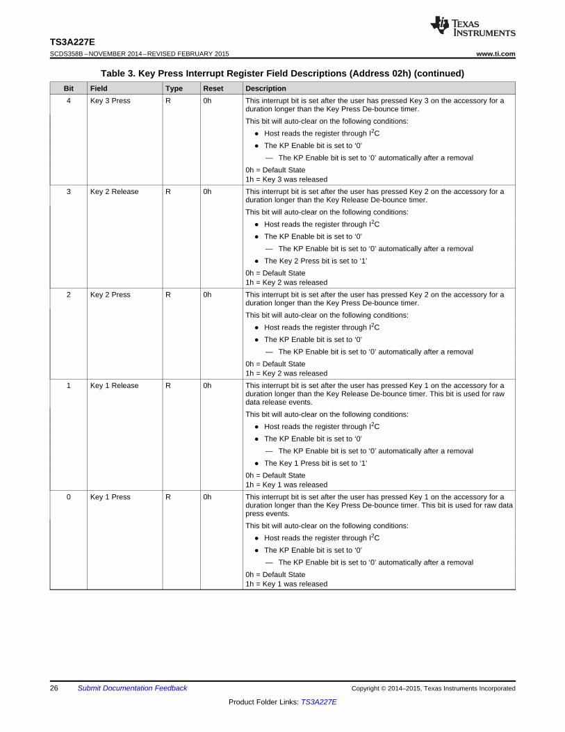
Table 3. Key Press Interrupt Register Field Descriptions (Address 02h) (continued)Bit Field Type Reset Description4 Key 3 Press R 0h This interrupt bit is set after the user has pressed Key 3 on the accessory for a
duration longer than the Key Press De-bounce timer.This bit will auto-clear on the following conditions:
● Host reads the register through I2C● The KP Enable bit is set to ‘0’
— The KP Enable bit is set to ‘0’ automatically after a removal0h = Default State1h = Key 3 was released
3 Key 2 Release R 0h This interrupt bit is set after the user has pressed Key 2 on the accessory for aduration longer than the Key Release De-bounce timer.This bit will auto-clear on the following conditions:
● Host reads the register through I2C● The KP Enable bit is set to ‘0’
— The KP Enable bit is set to ‘0’ automatically after a removal● The Key 2 Press bit is set to ‘1’
0h = Default State1h = Key 2 was released
2 Key 2 Press R 0h This interrupt bit is set after the user has pressed Key 2 on the accessory for aduration longer than the Key Press De-bounce timer.This bit will auto-clear on the following conditions:
● Host reads the register through I2C● The KP Enable bit is set to ‘0’
— The KP Enable bit is set to ‘0’ automatically after a removal0h = Default State1h = Key 2 was released
1 Key 1 Release R 0h This interrupt bit is set after the user has pressed Key 1 on the accessory for aduration longer than the Key Release De-bounce timer. This bit is used for rawdata release events.This bit will auto-clear on the following conditions:
● Host reads the register through I2C● The KP Enable bit is set to ‘0’
— The KP Enable bit is set to ‘0’ automatically after a removal● The Key 1 Press bit is set to ‘1’
0h = Default State1h = Key 1 was released
0 Key 1 Press R 0h This interrupt bit is set after the user has pressed Key 1 on the accessory for aduration longer than the Key Press De-bounce timer. This bit is used for raw datapress events.This bit will auto-clear on the following conditions:
● Host reads the register through I2C● The KP Enable bit is set to ‘0’
— The KP Enable bit is set to ‘0’ automatically after a removal0h = Default State1h = Key 1 was released
26 Submit Documentation Feedback Copyright © 2014–2015, Texas Instruments Incorporated
Product Folder Links: TS3A227E
TS3A227Ewww.ti.com SCDS358B –NOVEMBER 2014–REVISED FEBRUARY 2015
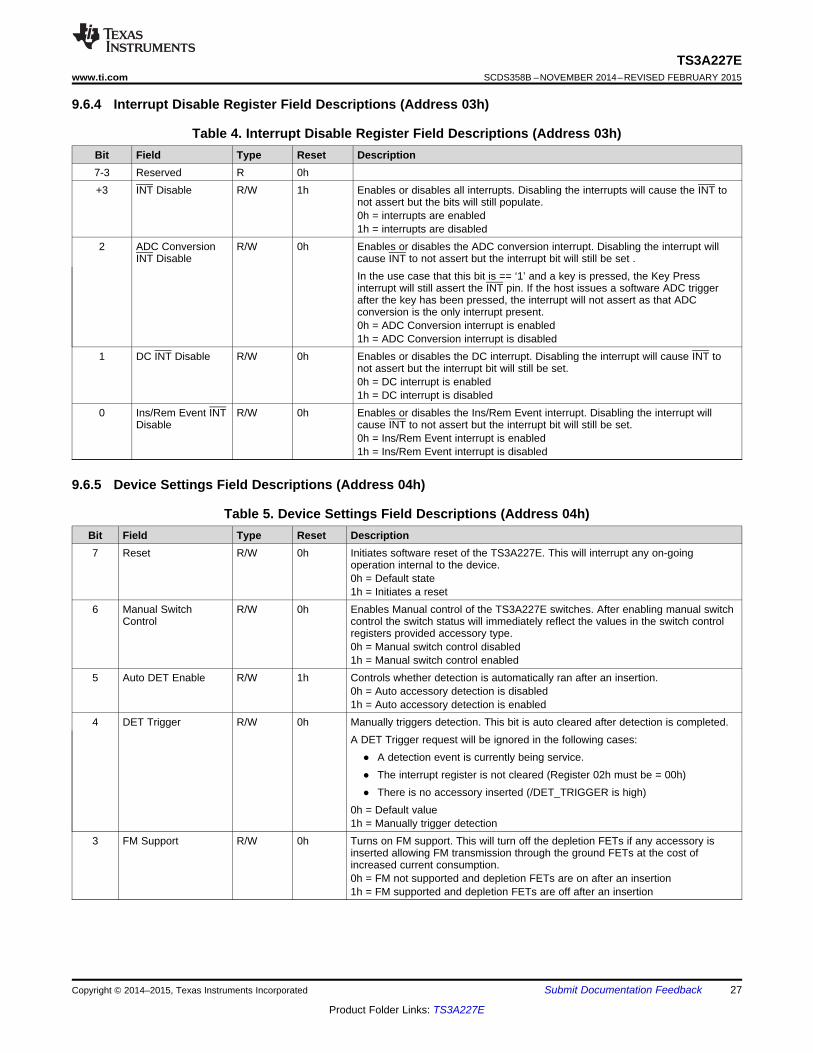
9.6.4 Interrupt Disable Register Field Descriptions (Address 03h)
Table 4. Interrupt Disable Register Field Descriptions (Address 03h)Bit Field Type Reset Description7-3 Reserved R 0h+3 INT Disable R/W 1h Enables or disables all interrupts. Disabling the interrupts will cause the INT to
not assert but the bits will still populate.0h = interrupts are enabled1h = interrupts are disabled
2 ADC Conversion R/W 0h Enables or disables the ADC conversion interrupt. Disabling the interrupt willINT Disable cause INT to not assert but the interrupt bit will still be set .
In the use case that this bit is == ‘1’ and a key is pressed, the Key Pressinterrupt will still assert the INT pin. If the host issues a software ADC triggerafter the key has been pressed, the interrupt will not assert as that ADCconversion is the only interrupt present.0h = ADC Conversion interrupt is enabled1h = ADC Conversion interrupt is disabled
1 DC INT Disable R/W 0h Enables or disables the DC interrupt. Disabling the interrupt will cause INT tonot assert but the interrupt bit will still be set.0h = DC interrupt is enabled1h = DC interrupt is disabled
0 Ins/Rem Event INT R/W 0h Enables or disables the Ins/Rem Event interrupt. Disabling the interrupt willDisable cause INT to not assert but the interrupt bit will still be set.
0h = Ins/Rem Event interrupt is enabled1h = Ins/Rem Event interrupt is disabled
9.6.5 Device Settings Field Descriptions (Address 04h)
Table 5. Device Settings Field Descriptions (Address 04h)Bit Field Type Reset Description7 Reset R/W 0h Initiates software reset of the TS3A227E. This will interrupt any on-going
operation internal to the device.0h = Default state1h = Initiates a reset
6 Manual Switch R/W 0h Enables Manual control of the TS3A227E switches. After enabling manual switchControl control the switch status will immediately reflect the values in the switch control
registers provided accessory type.0h = Manual switch control disabled1h = Manual switch control enabled
5 Auto DET Enable R/W 1h Controls whether detection is automatically ran after an insertion.0h = Auto accessory detection is disabled1h = Auto accessory detection is enabled
4 DET Trigger R/W 0h Manually triggers detection. This bit is auto cleared after detection is completed.A DET Trigger request will be ignored in the following cases:● A detection event is currently being service.● The interrupt register is not cleared (Register 02h must be = 00h)● There is no accessory inserted (/DET_TRIGGER is high)
0h = Default value1h = Manually trigger detection
3 FM Support R/W 0h Turns on FM support. This will turn off the depletion FETs if any accessory isinserted allowing FM transmission through the ground FETs at the cost ofincreased current consumption.0h = FM not supported and depletion FETs are on after an insertion1h = FM supported and depletion FETs are off after an insertion
Copyright © 2014–2015, Texas Instruments Incorporated Submit Documentation Feedback 27
Product Folder Links: TS3A227E
TS3A227ESCDS358B –NOVEMBER 2014–REVISED FEBRUARY 2015 www.ti.com
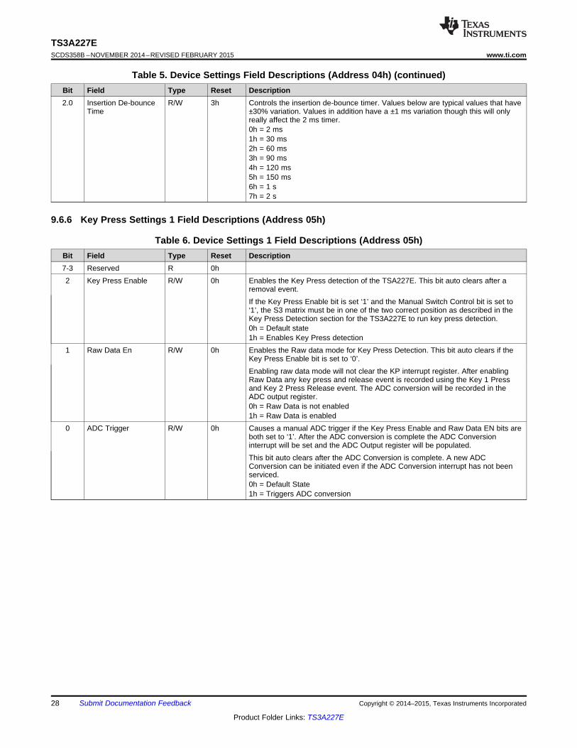
Table 5. Device Settings Field Descriptions (Address 04h) (continued)Bit Field Type Reset Description2.0 Insertion De-bounce R/W 3h Controls the insertion de-bounce timer. Values below are typical values that have
Time ±30% variation. Values in addition have a ±1 ms variation though this will onlyreally affect the 2 ms timer.0h = 2 ms1h = 30 ms2h = 60 ms3h = 90 ms4h = 120 ms5h = 150 ms6h = 1 s7h = 2 s
9.6.6 Key Press Settings 1 Field Descriptions (Address 05h)
Table 6. Device Settings 1 Field Descriptions (Address 05h)Bit Field Type Reset Description7-3 Reserved R 0h2 Key Press Enable R/W 0h Enables the Key Press detection of the TSA227E. This bit auto clears after a
removal event.If the Key Press Enable bit is set ‘1’ and the Manual Switch Control bit is set to‘1’, the S3 matrix must be in one of the two correct position as described in theKey Press Detection section for the TS3A227E to run key press detection.0h = Default state1h = Enables Key Press detection
1 Raw Data En R/W 0h Enables the Raw data mode for Key Press Detection. This bit auto clears if theKey Press Enable bit is set to ‘0’.Enabling raw data mode will not clear the KP interrupt register. After enablingRaw Data any key press and release event is recorded using the Key 1 Pressand Key 2 Press Release event. The ADC conversion will be recorded in theADC output register.0h = Raw Data is not enabled1h = Raw Data is enabled
0 ADC Trigger R/W 0h Causes a manual ADC trigger if the Key Press Enable and Raw Data EN bits areboth set to ‘1’. After the ADC conversion is complete the ADC Conversioninterrupt will be set and the ADC Output register will be populated.This bit auto clears after the ADC Conversion is complete. A new ADCConversion can be initiated even if the ADC Conversion interrupt has not beenserviced.0h = Default State1h = Triggers ADC conversion
28 Submit Documentation Feedback Copyright © 2014–2015, Texas Instruments Incorporated
Product Folder Links: TS3A227E
TS3A227Ewww.ti.com SCDS358B –NOVEMBER 2014–REVISED FEBRUARY 2015
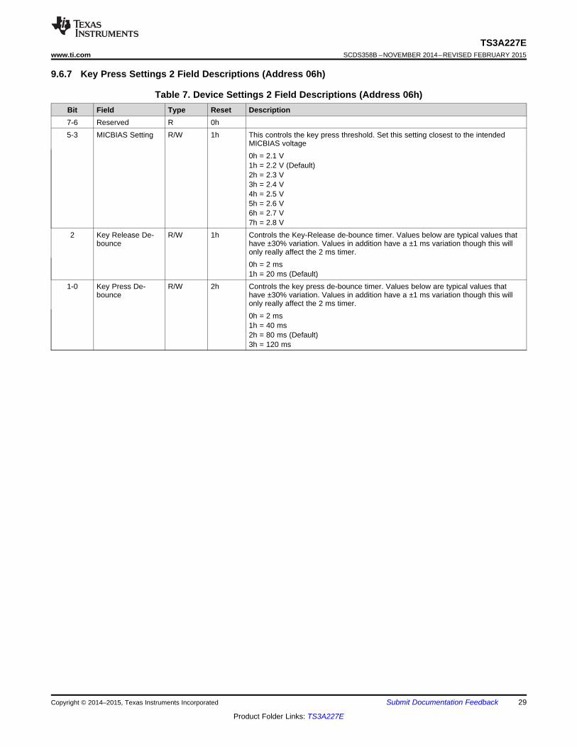
9.6.7 Key Press Settings 2 Field Descriptions (Address 06h)
Table 7. Device Settings 2 Field Descriptions (Address 06h)Bit Field Type Reset Description7-6 Reserved R 0h5-3 MICBIAS Setting R/W 1h This controls the key press threshold. Set this setting closest to the intended
MICBIAS voltage0h = 2.1 V1h = 2.2 V (Default)2h = 2.3 V3h = 2.4 V4h = 2.5 V5h = 2.6 V6h = 2.7 V7h = 2.8 V
2 Key Release De- R/W 1h Controls the Key-Release de-bounce timer. Values below are typical values thatbounce have ±30% variation. Values in addition have a ±1 ms variation though this will
only really affect the 2 ms timer.0h = 2 ms1h = 20 ms (Default)
1-0 Key Press De- R/W 2h Controls the key press de-bounce timer. Values below are typical values thatbounce have ±30% variation. Values in addition have a ±1 ms variation though this will
only really affect the 2 ms timer.0h = 2 ms1h = 40 ms2h = 80 ms (Default)3h = 120 ms
Copyright © 2014–2015, Texas Instruments Incorporated Submit Documentation Feedback 29
Product Folder Links: TS3A227E
TS3A227ESCDS358B –NOVEMBER 2014–REVISED FEBRUARY 2015 www.ti.com
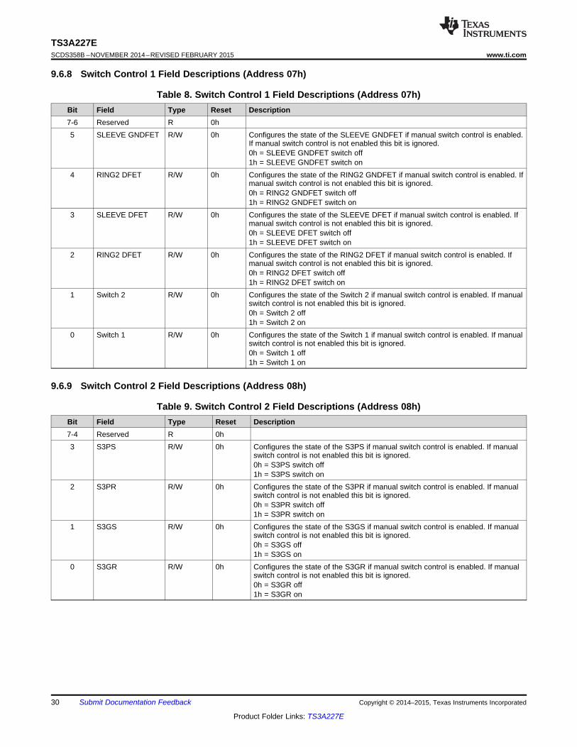
9.6.8 Switch Control 1 Field Descriptions (Address 07h)
Table 8. Switch Control 1 Field Descriptions (Address 07h)Bit Field Type Reset Description7-6 Reserved R 0h5 SLEEVE GNDFET R/W 0h Configures the state of the SLEEVE GNDFET if manual switch control is enabled.
If manual switch control is not enabled this bit is ignored.0h = SLEEVE GNDFET switch off1h = SLEEVE GNDFET switch on
4 RING2 DFET R/W 0h Configures the state of the RING2 GNDFET if manual switch control is enabled. Ifmanual switch control is not enabled this bit is ignored.0h = RING2 GNDFET switch off1h = RING2 GNDFET switch on
3 SLEEVE DFET R/W 0h Configures the state of the SLEEVE DFET if manual switch control is enabled. Ifmanual switch control is not enabled this bit is ignored.0h = SLEEVE DFET switch off1h = SLEEVE DFET switch on
2 RING2 DFET R/W 0h Configures the state of the RING2 DFET if manual switch control is enabled. Ifmanual switch control is not enabled this bit is ignored.0h = RING2 DFET switch off1h = RING2 DFET switch on
1 Switch 2 R/W 0h Configures the state of the Switch 2 if manual switch control is enabled. If manualswitch control is not enabled this bit is ignored.0h = Switch 2 off1h = Switch 2 on
0 Switch 1 R/W 0h Configures the state of the Switch 1 if manual switch control is enabled. If manualswitch control is not enabled this bit is ignored.0h = Switch 1 off1h = Switch 1 on
9.6.9 Switch Control 2 Field Descriptions (Address 08h)
Table 9. Switch Control 2 Field Descriptions (Address 08h)Bit Field Type Reset Description7-4 Reserved R 0h3 S3PS R/W 0h Configures the state of the S3PS if manual switch control is enabled. If manual
switch control is not enabled this bit is ignored.0h = S3PS switch off1h = S3PS switch on
2 S3PR R/W 0h Configures the state of the S3PR if manual switch control is enabled. If manualswitch control is not enabled this bit is ignored.0h = S3PR switch off1h = S3PR switch on
1 S3GS R/W 0h Configures the state of the S3GS if manual switch control is enabled. If manualswitch control is not enabled this bit is ignored.0h = S3GS off1h = S3GS on
0 S3GR R/W 0h Configures the state of the S3GR if manual switch control is enabled. If manualswitch control is not enabled this bit is ignored.0h = S3GR off1h = S3GR on
30 Submit Documentation Feedback Copyright © 2014–2015, Texas Instruments Incorporated
Product Folder Links: TS3A227E
TS3A227Ewww.ti.com SCDS358B –NOVEMBER 2014–REVISED FEBRUARY 2015
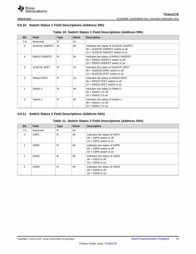
9.6.10 Switch Status 1 Field Descriptions (Address 09h)
Table 10. Switch Status 1 Field Descriptions (Address 09h)Bit Field Type Reset Description7-6 Reserved R 0h5 SLEEVE GNDFET R 0h Indicates the status of SLEEVE GNDFET
0h = SLEEVE GNDFET switch is off1h = SLEEVE GNDFET switch is on
4 RING2 GNDFET R 0h Indicates the status of RING2 GNDFET0h = RING2 GNDFET switch is off1h = RING2 GNDFET switch is on
3 SLEEVE DFET R 1h Indicates the status of SLEEVE DFET0h = SLEEVE DFET switch is off1h = SLEEVE DFET switch is on
2 RING2 DFET R 1h Indicates the status of RING2 DFET0h = RING2 DFET switch is off1h = RING2 DFET switch is on
1 Switch 2 R 0h Indicates the status of Switch 20h = Switch 2 is off1h = Switch 2 is on
0 Switch 1 R 0h Indicates the status of Switch 10h = Switch 1 is off1h = Switch 1 is on
9.6.11 Switch Status 2 Field Descriptions (Address 0Ah)
Table 11. Switch Status 2 Field Descriptions (Address 0Ah)Bit Field Type Reset Description7-4 Reserved R 0h3 S3PS R 0h Indicates the status of S3PS
0h = S3PS switch is off1h = S3PS switch is on
2 S3PR R 0h Indicates the status of S3PR0h = S3PR switch is off1h = S3PR switch is on
1 S3GS R 0h Indicates the status of S3GS0h = S3GS is off1h = S3GS is on
0 S3GR R 0h Indicates the status of S3GR0h = S3GR is off1h = S3GR is on
Copyright © 2014–2015, Texas Instruments Incorporated Submit Documentation Feedback 31
Product Folder Links: TS3A227E
TS3A227ESCDS358B –NOVEMBER 2014–REVISED FEBRUARY 2015 www.ti.com
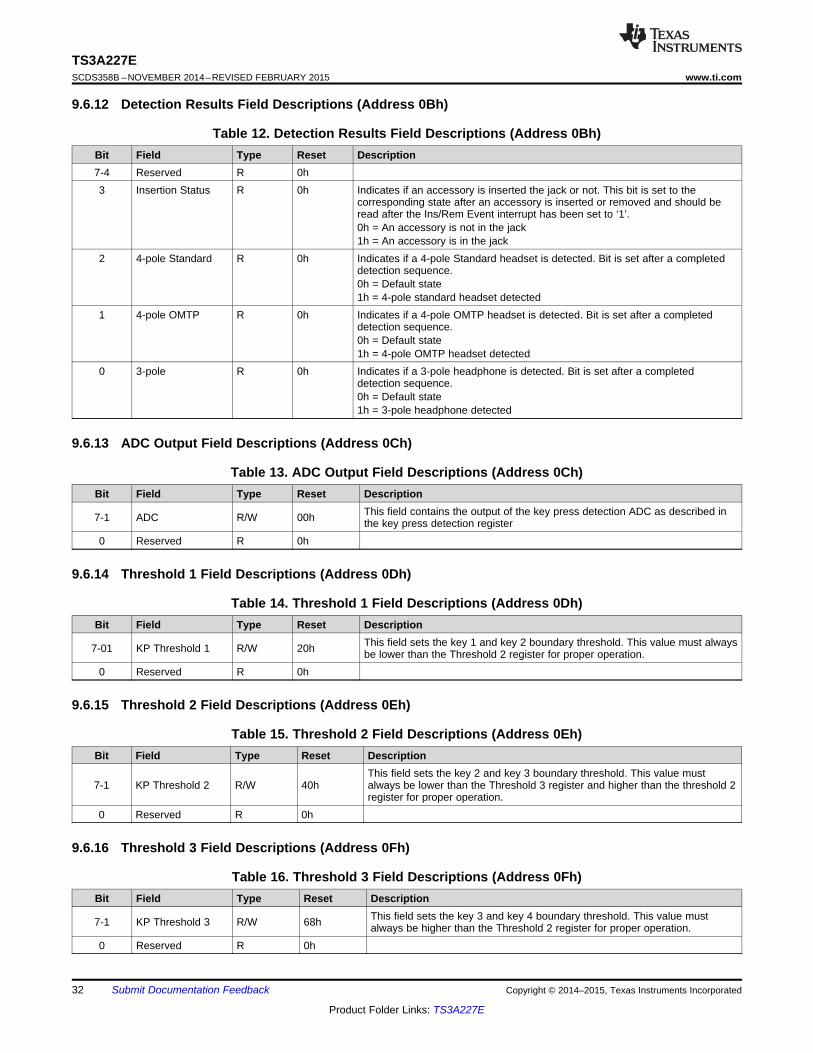
9.6.12 Detection Results Field Descriptions (Address 0Bh)
Table 12. Detection Results Field Descriptions (Address 0Bh)Bit Field Type Reset Description7-4 Reserved R 0h3 Insertion Status R 0h Indicates if an accessory is inserted the jack or not. This bit is set to the
corresponding state after an accessory is inserted or removed and should beread after the Ins/Rem Event interrupt has been set to ‘1’.0h = An accessory is not in the jack1h = An accessory is in the jack
2 4-pole Standard R 0h Indicates if a 4-pole Standard headset is detected. Bit is set after a completeddetection sequence.0h = Default state1h = 4-pole standard headset detected
1 4-pole OMTP R 0h Indicates if a 4-pole OMTP headset is detected. Bit is set after a completeddetection sequence.0h = Default state1h = 4-pole OMTP headset detected
0 3-pole R 0h Indicates if a 3-pole headphone is detected. Bit is set after a completeddetection sequence.0h = Default state1h = 3-pole headphone detected
9.6.13 ADC Output Field Descriptions (Address 0Ch)
Table 13. ADC Output Field Descriptions (Address 0Ch)Bit Field Type Reset Description
This field contains the output of the key press detection ADC as described in7-1 ADC R/W 00h the key press detection register0 Reserved R 0h
9.6.14 Threshold 1 Field Descriptions (Address 0Dh)
Table 14. Threshold 1 Field Descriptions (Address 0Dh)Bit Field Type Reset Description
This field sets the key 1 and key 2 boundary threshold. This value must always7-01 KP Threshold 1 R/W 20h be lower than the Threshold 2 register for proper operation.0 Reserved R 0h
9.6.15 Threshold 2 Field Descriptions (Address 0Eh)
Table 15. Threshold 2 Field Descriptions (Address 0Eh)Bit Field Type Reset Description
This field sets the key 2 and key 3 boundary threshold. This value must7-1 KP Threshold 2 R/W 40h always be lower than the Threshold 3 register and higher than the threshold 2
register for proper operation.0 Reserved R 0h
9.6.16 Threshold 3 Field Descriptions (Address 0Fh)
Table 16. Threshold 3 Field Descriptions (Address 0Fh)Bit Field Type Reset Description
This field sets the key 3 and key 4 boundary threshold. This value must7-1 KP Threshold 3 R/W 68h always be higher than the Threshold 2 register for proper operation.0 Reserved R 0h
32 Submit Documentation Feedback Copyright © 2014–2015, Texas Instruments Incorporated
Product Folder Links: TS3A227E
4
16
9
3
13
6
5
1 2
11
10
12
8
7
14
15
MIC_PRESENT
SCL
SDA
INT
MICP
GND_SENSE
VDD
RING 2_SENSE
SLEEVE_SENSE
TIP
DET_TRIGGER
RING2
SLEEVE
GND
GNDA
GND
L1
C4
FM Network
R5
R6C3
GND_SENSE
MICI
MICBIAS
Application
Processor
C1 C2
3.3 V
R4
R1R2
R3
TS3A227ERVAR
TS3A227Ewww.ti.com SCDS358B –NOVEMBER 2014–REVISED FEBRUARY 2015
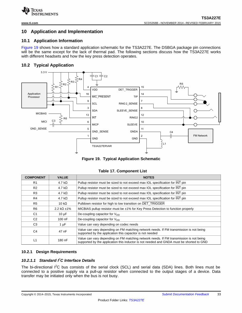
10 Application and Implementation
10.1 Application InformationFigure 19 shows how a standard application schematic for the TS3A227E. The DSBGA package pin connectionswill be the same except for the lack of thermal pad. The following sections discuss how the TS3A227E workswith different headsets and how the key press detection operates.
10.2 Typical Application
Figure 19. Typical Application Schematic
Table 17. Component ListCOMPONENT VALUE NOTES
R1 4.7 kΩ Pullup resistor must be sized to not exceed max IOL specification for INT pinR2 4.7 kΩ Pullup resistor must be sized to not exceed max IOL specification for INT pinR3 4.7 kΩ Pullup resistor must be sized to not exceed max IOL specification for INT pinR4 4.7 kΩ Pullup resistor must be sized to not exceed max IOL specification for INT pinR5 10 kΩ Pulldown resistor for high to low transition on DET_TRIGGERR6 2.2 kΩ ±1% MICBIAS pullup resistor must be ±1% for Key Press Detection to function properlyC1 10 µF De-coupling capacitor for VDD
C2 100 nF De-coupling capacitor for VDD
C3 1 µF Value can vary depending on codec needsValue can vary depending on FM matching network needs. If FM transmission is not beingC4 47 nF supported by the application this capacitor is not neededValue can vary depending on FM matching network needs. If FM transmission is not beingL1 180 nF supported by the application this inductor is not needed and GNDA must be shorted to GND
10.2.1 Design Requirements
10.2.1.1 Standard I2C Interface DetailsThe bi-directional I2C bus consists of the serial clock (SCL) and serial data (SDA) lines. Both lines must beconnected to a positive supply via a pull-up resistor when connected to the output stages of a device. Datatransfer may be initiated only when the bus is not busy.
Copyright © 2014–2015, Texas Instruments Incorporated Submit Documentation Feedback 33
Product Folder Links: TS3A227E
ST A6 A5 A4 A3 A2 A1 A0 0
START R/W
ACK From slave
A 0 0 0 0 0 0 0 0 A
Auto Increment
Register Address N
Slave Address Sub Address
ACK From slave
D7 D6 D5 D4 D3 D2 D1 D0 A
Data to Register N
Data Byte
ACK From slave
D7 D6 D5 D4 D3 D2 D1 D0 A
Data to Register N
Data Byte
ACK From slave
SP
STOP
1 2 8 9
Clock pulse for
acknowledgment
SCL
ST
Start
Condition
SDA Output
by
Transmitter
SDA Output
by Receiver
NACK
ACK
TS3A227ESCDS358B –NOVEMBER 2014–REVISED FEBRUARY 2015 www.ti.com
I2C communication with this device is initiated by the master sending a START condition, a high-to-low transitionon the SDA line while the SCL line is high. After the start condition, the device address byte is send, MSB first,including the data direction bit (R/W). This device does not respond to the general call address. After receivingthe valid address byte (0x77 read, 0x76 write), this device responds with an ACK, a low on the SDA line duringthe high of the ACK-related clock pulse.
The data byte follows the address ACK. The R/W bit is kept low for transfer from the master to the slave. Thedata byte is followed by an ACK sent from this device. Data are output only if complete bytes are received andacknowledged. The output data is valid at time (tpv) after the low-to-high transition of SCL, during the clock cyclefor the ACK.
On the I2C bus, only one data bit is transferred during each clock pulse. The data on the SDA line must remainstable during the high pulse of the clock period, as changes in the data line at this time are interpreted as controlcommands (START or STOP).
A Stop condition, a low-to-high transition on the SDA line while the SCL line is high, is sent by the master. Thenumber of data bytes transferred between the start and the stop conditions from the transmitter to receiver is notlimited. Each byte of eight bits is followed by one ACK bit. The transmitter must release the SDA line before thereceiver can send an ACK bit.
A slave receiver that is addressed must generate an ACK after the reception of each byte. The device thatacknowledges has to pull down the SDA line during the ACK clock pulse so that the SDA line is stable low duringthe high pulse of the ACK-related clock period. Setup and fold times must be taken into account.
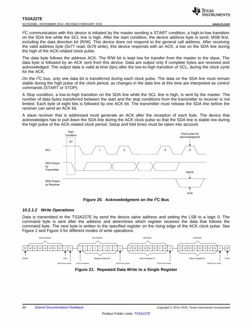
Figure 20. Acknowledgment on the I2C Bus
10.2.1.2 Write OperationsData is transmitted to the TS3A227E by send the device salve address and setting the LSB to a logic 0. Thecommand byte is sent after the address and determines which register receives the data that follows thecommand byte. The next byte is written to the specified register on the rising edge of the ACK clock pulse. SeeFigure 2 and Figure 3 for different modes of write operations.
Figure 21. Repeated Data Write to a Single Register
34 Submit Documentation Feedback Copyright © 2014–2015, Texas Instruments Incorporated
Product Folder Links: TS3A227E
ST A6 A5 A4 A3 A2 A1 A0 0
START R/W
ACK From slave
A 0 0 0 0 0 0 0 0 A
Auto Increment
Register Address N
Slave Address Sub Address
ACK From slave
RS
Re-start
A6 A5 A4 A3 A2 A1 A0 1
R/W
ACK From slave
A
Slave Address
D7 D6 D5 D4 D3 D2 D1 D0 A
Data from Register N
Data Byte
ACK From master
D7 D6 D5 D4 D3 D2 D1 D0 A
Data from Register N
Data Byte
ACK From master
D7 D6 D5 D4 D3 D2 D1 D0 NA
Data from Register N
Data Byte
NACK From master
SP
Stop
TS3A227Ewww.ti.com SCDS358B –NOVEMBER 2014–REVISED FEBRUARY 2015
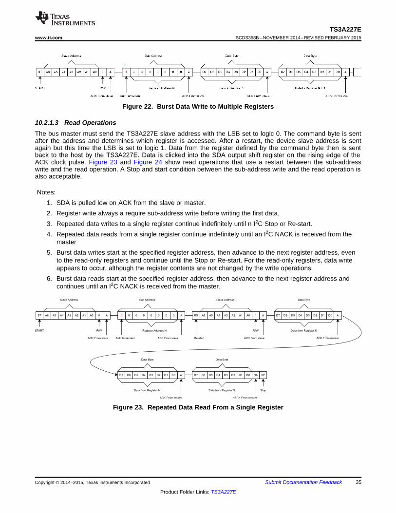
Figure 22. Burst Data Write to Multiple Registers
10.2.1.3 Read OperationsThe bus master must send the TS3A227E slave address with the LSB set to logic 0. The command byte is sentafter the address and determines which register is accessed. After a restart, the device slave address is sentagain but this time the LSB is set to logic 1. Data from the register defined by the command byte then is sentback to the host by the TS3A227E. Data is clicked into the SDA output shift register on the rising edge of theACK clock pulse. Figure 23 and Figure 24 show read operations that use a restart between the sub-addresswrite and the read operation. A Stop and start condition between the sub-address write and the read operation isalso acceptable.
Notes:1. SDA is pulled low on ACK from the slave or master.2. Register write always a require sub-address write before writing the first data.3. Repeated data writes to a single register continue indefinitely until n I2C Stop or Re-start.4. Repeated data reads from a single register continue indefinitely until an I2C NACK is received from the
master5. Burst data writes start at the specified register address, then advance to the next register address, even
to the read-only registers and continue until the Stop or Re-start. For the read-only registers, data writeappears to occur, although the register contents are not changed by the write operations.
6. Burst data reads start at the specified register address, then advance to the next register address andcontinues until an I2C NACK is received from the master.
Figure 23. Repeated Data Read From a Single Register
Copyright © 2014–2015, Texas Instruments Incorporated Submit Documentation Feedback 35
Product Folder Links: TS3A227E
TS3A227E
MICP
GND_SENSE
S3PRRING 2
SLEEVE
S3PS
S3GS
S3GR
S1 S2RING2
GNDFET
SLEEVE
GNDFET
RING2
DFET
SLEEVE
DFET
GND GNDGNDA
Audio Jack
RING1
TIPL R ? ?
DET_TRIGGER
High to Low
VDD
ST A6 A5 A4 A3 A2 A1 A0 0
START R/W
ACK From slave
A 0 0 0 0 0 0 0 0 A
Auto Increment
Register Address N
Slave Address Sub Address
ACK From slave
RS
Re-start
A6 A5 A4 A3 A2 A1 A0 1
R/W
ACK From slave
A
Slave Address
D7 D6 D5 D4 D3 D2 D1 D0 A
Data from Register N
Data Byte
ACK From master
D7 D6 D5 D4 D3 D2 D1 D0 A
Data from Register N
Data Byte
ACK From master
D7 D6 D5 D4 D3 D2 D1 D0 NA
Data from Register N
Data Byte
NACK From master
SP
Stop
TS3A227ESCDS358B –NOVEMBER 2014–REVISED FEBRUARY 2015 www.ti.com
Figure 24. Burst Data Read From Multiple Registers
10.2.2 Detailed Design Procedure
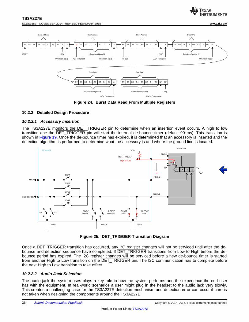
10.2.2.1 Accessory InsertionThe TS3A227E monitors the DET_TRIGGER pin to determine when an insertion event occurs. A high to lowtransition one the DET_TRIGGER pin will start the internal de-bounce timer (default 90 ms). This transition isshown in Figure 19. Once the de-bounce timer has expired, it is determined that an accessory is inserted and thedetection algorithm is performed to determine what the accessory is and where the ground line is located.
Figure 25. DET_TRIGGER Transition Diagram
Once a DET_TRIGGER transition has occurred, any I2C register changes will not be serviced until after the de-bounce and detection sequence have completed. If DET_TRIGGER transitions from Low to High before the de-bounce period has expired. The I2C register changes will be serviced before a new de-bounce timer is startedfrom another High to Low transition on the DET_TRIGGER pin. The I2C communication has to complete beforethe next High to Low transition to take effect.
10.2.2.2 Audio Jack SelectionThe audio jack the system uses plays a key role in how the system performs and the experience the end userhas with the equipment. In real-world scenarios a user might plug in the headset to the audio jack very slowly.This creates a challenging case for the TS3A227E detection mechanism and detection error can occur if care isnot taken when designing the components around the TS3A227E.
36 Submit Documentation Feedback Copyright © 2014–2015, Texas Instruments Incorporated
Product Folder Links: TS3A227E
TS3A227E
MICP
GND_SENSE
S3PR
SLEEVE
S3PS
S3GS
S3GR
S1 S2RING2
GNDFET
SLEEVE
GNDFET
RING2
DFET
SLEEVE
DFET
RING2
SLEEVE_SENSE
RING 2_SENSE
GND GNDGNDA
TS3A227Ewww.ti.com SCDS358B –NOVEMBER 2014–REVISED FEBRUARY 2015
The main concern for slow plug-in is the detection process may have already started before the headset is fullyinserted into the jack. If the detection is running with the headset out of position, a false impedancemeasurement may occur. For best performance a jack should be chosen that puts the detection mechanism onthe TIP pin at the end of physical jack to ensure that it is fully inserted.
The TS3A227E EVM contains test points for all the jack pins and can be blue wired to prototype audio jacks fortesting.
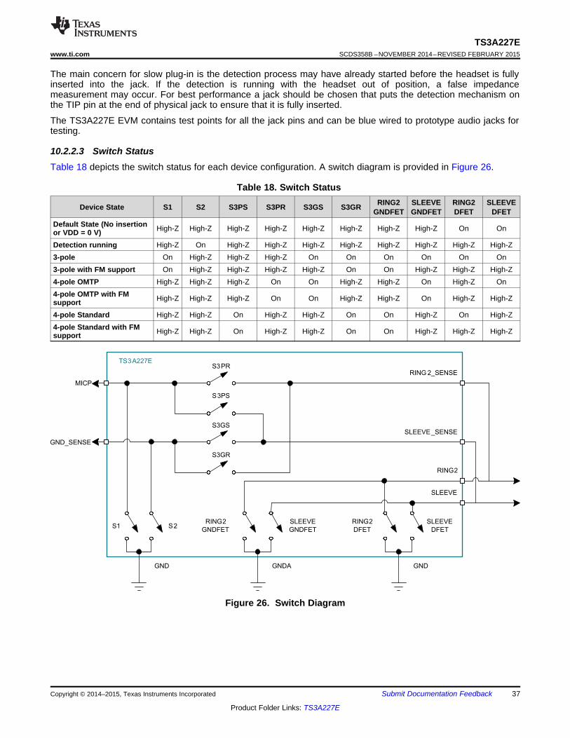
10.2.2.3 Switch StatusTable 18 depicts the switch status for each device configuration. A switch diagram is provided in Figure 26.
Table 18. Switch StatusRING2 SLEEVE RING2 SLEEVEDevice State S1 S2 S3PS S3PR S3GS S3GR GNDFET GNDFET DFET DFET
Default State (No insertion High-Z High-Z High-Z High-Z High-Z High-Z High-Z High-Z On Onor VDD = 0 V)Detection running High-Z On High-Z High-Z High-Z High-Z High-Z High-Z High-Z High-Z3-pole On High-Z High-Z High-Z On On On On On On3-pole with FM support On High-Z High-Z High-Z High-Z On On High-Z High-Z High-Z4-pole OMTP High-Z High-Z High-Z On On High-Z High-Z On High-Z On4-pole OMTP with FM High-Z High-Z High-Z On On High-Z High-Z On High-Z High-Zsupport4-pole Standard High-Z High-Z On High-Z High-Z On On High-Z On High-Z4-pole Standard with FM High-Z High-Z On High-Z High-Z On On High-Z High-Z High-Zsupport
Figure 26. Switch Diagram
Copyright © 2014–2015, Texas Instruments Incorporated Submit Documentation Feedback 37
Product Folder Links: TS3A227E
TS3A227E
MICP
GND_SENSE
S3PR
SLEEVE
S3PS
S3GS
S3GR
S1 S2RING2
GNDFET
SLEEVE
GNDFET
RING2
DFET
SLEEVE
DFET
RING2
SLEEVE_SENSE
RING 2_SENSE
GND GNDGNDA
Audio Jack
L R ? ?
TS3A227E
MICP
GND_SENSE
S3PR
SLEEVE
S3PS
S3GS
S3GR
S1 S2RING2
GNDFET
SLEEVE
GNDFET
RING2
DFET
SLEEVE
DFET
RING2
SLEEVE_SENSE
RING 2_SENSE
GND GNDGNDA
Audio Jack
TS3A227ESCDS358B –NOVEMBER 2014–REVISED FEBRUARY 2015 www.ti.com
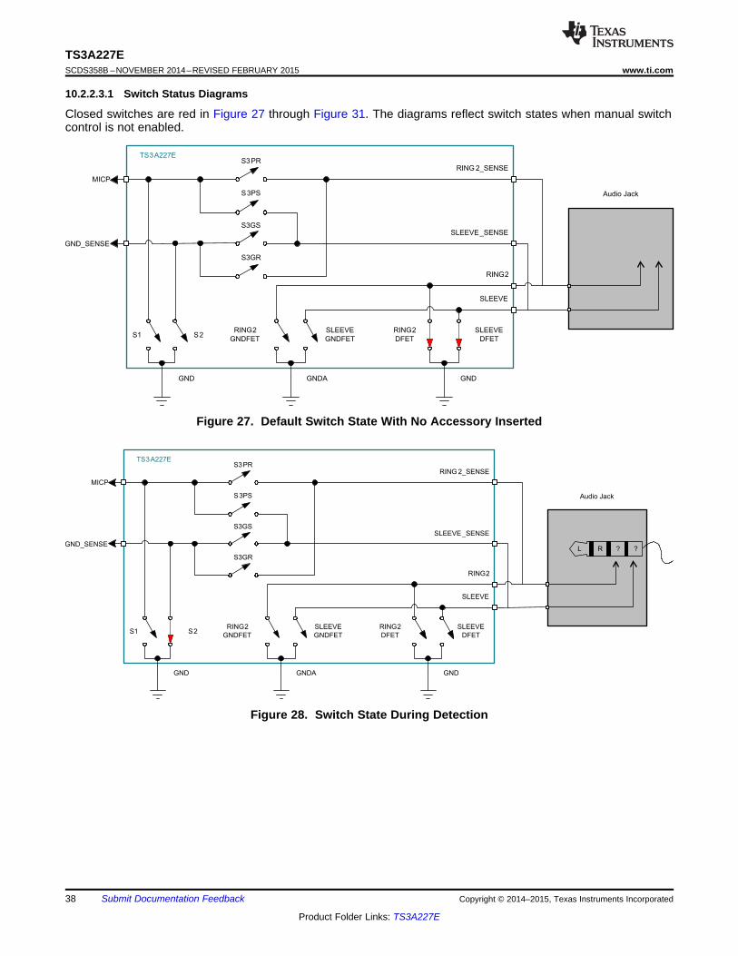
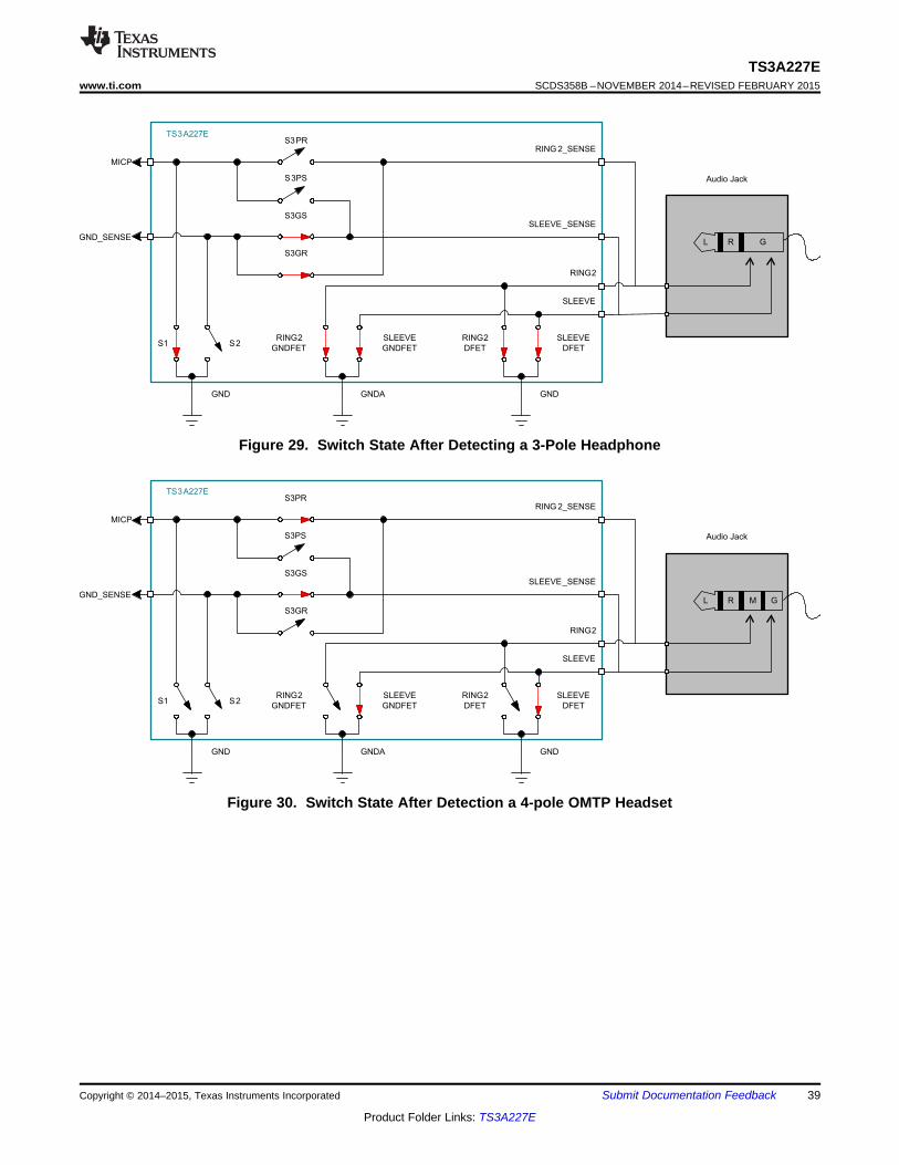
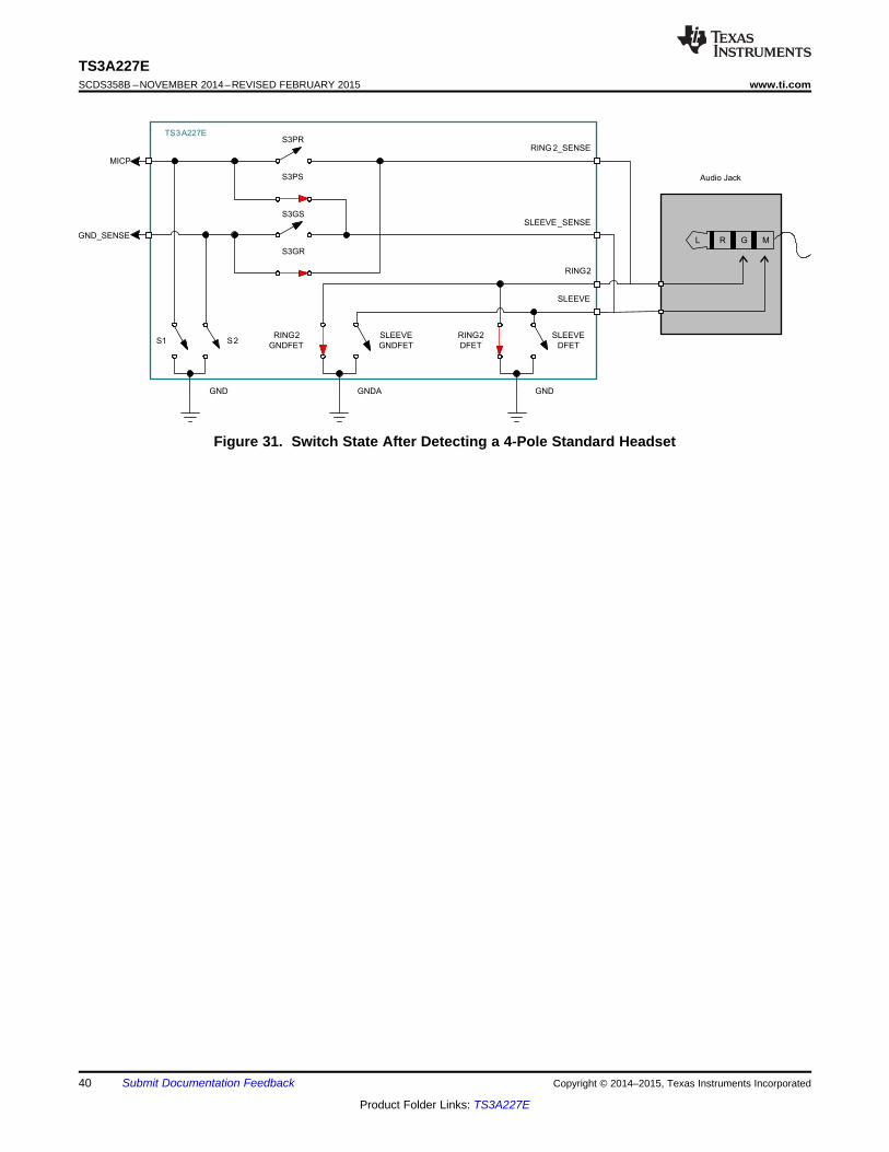
10.2.2.3.1 Switch Status Diagrams
Closed switches are red in Figure 27 through Figure 31. The diagrams reflect switch states when manual switchcontrol is not enabled.
Figure 27. Default Switch State With No Accessory Inserted
Figure 28. Switch State During Detection
38 Submit Documentation Feedback Copyright © 2014–2015, Texas Instruments Incorporated
Product Folder Links: TS3A227E
TS3A227E
MICP
GND_SENSE
S3PR
SLEEVE
S3PS
S3GS
S3GR
S1 S2RING2
GNDFET
SLEEVE
GNDFET
RING2
DFET
SLEEVE
DFET
RING2
SLEEVE_SENSE
RING 2_SENSE
GND GNDGNDA
Audio Jack
L R M G
TS3A227E
MICP
GND_SENSE
S3PR
SLEEVE
S3PS
S3GS
S3GR
S1 S2RING2
GNDFET
SLEEVE
GNDFET
RING2
DFET
SLEEVE
DFET
RING2
SLEEVE_SENSE
RING 2_SENSE
GND GNDGNDA
Audio Jack
L R G
TS3A227Ewww.ti.com SCDS358B –NOVEMBER 2014–REVISED FEBRUARY 2015
Figure 29. Switch State After Detecting a 3-Pole Headphone
Figure 30. Switch State After Detection a 4-pole OMTP Headset
Copyright © 2014–2015, Texas Instruments Incorporated Submit Documentation Feedback 39
Product Folder Links: TS3A227E
TS3A227E
MICP
GND_SENSE
S3PR
SLEEVE
S3PS
S3GS
S3GR
S1 S2RING2
GNDFET
SLEEVE
GNDFET
RING2
DFET
SLEEVE
DFET
RING2
SLEEVE_SENSE
RING 2_SENSE
GND GNDGNDA
Audio Jack
L R G M
TS3A227ESCDS358B –NOVEMBER 2014–REVISED FEBRUARY 2015 www.ti.com
Figure 31. Switch State After Detecting a 4-Pole Standard Headset
40 Submit Documentation Feedback Copyright © 2014–2015, Texas Instruments Incorporated
Product Folder Links: TS3A227E
2.2 kΩ
MICBIAS
Key2 Key3
MIC
Key4Key1
SLEEVE/RING2
TS3A227Ewww.ti.com SCDS358B –NOVEMBER 2014–REVISED FEBRUARY 2015
10.2.2.4 Key Press Detection
10.2.2.4.1 Key Press Thresholds
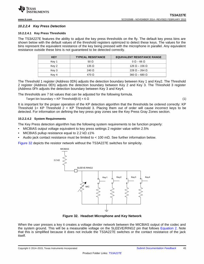
The TS3A227E features the ability to adjust the key press thresholds on the fly. The default key press bins areshown below with the default values of the threshold registers optimized to detect these keys. The values for thebins represent the equivalent resistance of the key being pressed with the microphone in parallel. Any equivalentresistance outside these bins is not guaranteed to be detected correctly.
KEY TYPICAL RESISTANCE EQUIVALENT RESISTANCE RANGEKey 1 50 Ω 0 Ω – 66 ΩKey 2 135 Ω 126 Ω – 156 ΩKey 3 240 Ω 228 Ω – 264 ΩKey 4 470 Ω 360 Ω – 680 Ω
The Threshold 1 register (Address 0Dh) adjusts the detection boundary between Key 1 and Key2. The Threshold2 register (Address 0Eh) adjusts the detection boundary between Key 2 and Key 3. The Threshold 3 register(Address 0Fh adjusts the detection boundary between Key 3 and Key4.
The thresholds are 7 bit values that can be adjusted for the following formula.Target bin boundary = KP Threshold[6:0] × 6 Ω (1)
It is important for the proper operation of the KP detection algorithm that the thresholds be ordered correctly: KPThreshold 1< KP Threshold 2 < KP Threshold 3. Placing them out of order will cause incorrect keys to bedetected. For information on defining the key press gray zones see the Key Press Gray Zones section.
10.2.2.4.2 System Requirements
The Key Press detection algorithm has the following system requirements to be function properly:• MICBIAS output voltage equivalent to key press settings 2 register value within 2.5%• MICBIAS pullup resistance equal to 2.2 kΩ ±1%• Audio jack contact resistance must be limited to < 100 mΩ. See further information below.
Figure 32 depicts the resistor network without the TS3A227E switches for simplicity.
Figure 32. Headset Microphone and Key Network
When the user presses a key it creates a voltage divider network between the MICBIAS output of the codec andthe system ground. This will be a measurable voltage on the SLEEVE/RING2 pin that follows Equation 2. Notethat this is simplified because it does not include the TS3A227E switches or the contact resistance of the jackitself.
Copyright © 2014–2015, Texas Instruments Incorporated Submit Documentation Feedback 41
Product Folder Links: TS3A227E
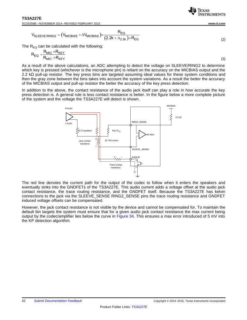
2.2 kΩ
Key R EQ
R Audio
L Audio
MICBIAS
32 Ω speakers
Jack contact
resistance
20-100 mohm
RING2_SENSE
SLEEVE _SENSE
SLEEVE
Trace routing
resistance
KP ADC
MIC KEYEQ
MIC KEY
R RR
R R
´
=
+
( )( )
EQSLEEVE/RING2 MICBIAS MICBIAS
2.2k EQ
RV V V
2.2k R= + D ´
+ D +
TS3A227ESCDS358B –NOVEMBER 2014–REVISED FEBRUARY 2015 www.ti.com
(2)
The REQ can be calculated with the following:
(3)
As a result of the above calculations, an ADC attempting to detect the voltage on SLEEVE/RING2 to determinewhich key is pressed (whichever is the microphone pin) is reliant on the accuracy on the MICBIAS output and the2.2 kΩ pull-up resistor. The key press bins are targeted assuming ideal values for these system conditions andthen the gray zone between the bins takes into account the system variations. As a result the better the accuracyof the MICBIAS output and pull-up resistor the better the accuracy of the key press detection.
In addition to the above, the contact resistance of the audio jack itself can play a role in how accurate the keypress detection is. A general rule is less contact resistance is better. In the figure below a more complete pictureof the system and the voltage the TS3A227E will detect is shown.
The red line denotes the current path for the output of the codec to follow when it enters the speakers andeventually sinks into the GNDFETs of the TS3A227E. This audio current adds a voltage offset at the audio jackcontact resistance, the trace routing resistance, and the GNDFET itself. Because the TS3A227E has kelvinconnections to the jack via the SLEEVE_SENSE RING2_SENSE pins the trace routing resistance and GNDFETinduced voltage offsets can be compensated.
However, the jack contact resistance is not visible by the device and cannot be compensated for. To maintain thedefault bin targets the system must ensure that for a given audio jack contact resistance the max current beingoutput by the codec/amplifier lies below the curve in Figure 34. This ensures a max error introduced of 5 mV intothe KP detection algorithm.
42 Submit Documentation Feedback Copyright © 2014–2015, Texas Instruments Incorporated
Product Folder Links: TS3A227E
5 mV 5 mVGray Zone 0.015 0.025 0.01 96 1.5 2 6
2.22.2
128
é ùæ öê úç ÷æ ö
= ± + + + ´ W+ + + ´ Wê úç ÷ç ÷è øê úç ÷ç ÷ê úè øë û
MICBIAS
Contact MAX
128
R I
V
´
Contact MAX
MICBIAS
R I
V
´
TS3A227Ewww.ti.com SCDS358B –NOVEMBER 2014–REVISED FEBRUARY 2015
10.2.2.4.3 Key Press Grey Zones
When defining custom bins and thresholds it is important to also correctly define the “gray zone” between thebins to ensure that the system will always correctly identify the key that is being pressed. The gray zone regionaccounts for the absolute error in key press detection, encompasses the error of the internal ADC along witherrors from system tolerances and variation. The equation below can be used to determine the gray zonerequired between each of the bins. Note that the size of the gray zone will vary depending on the actual value ofthe key press threshold.
Gray Zone = ± [(Ɛ(ADC,GAIN) + ƐMICBIAS + ƐRBIAS + Ɛ(CONT,GAIN) ) × R(KP Threshold) + (Ɛ(ADC,OFF) + Ɛ(CONT,OFF) + KBUFF ) × 6 Ω] (4)
TERM DESCRIPTION VALUE UNITƐ(ADC,GAIN) Internal ADC gain error 0.015%ƐMICBIAS Codec MICBIAS output voltage variation. Default bin values assume an output variation of 2.5%. 0.025% (1)
MICBIAS resistor variation. Default bin values assume a 1% tolerance of the 2.2 kΩ MICBIASƐRBIAS 0.01% (1)resistor.
ƐCONT.GAIN Gain error introduced by contact resistance of the audio jack.
KP threshold target identified by system. E.g. the KP Threshold between bins 1 and 2 for the Defined byƐKP Threshold Ωdefault key press bins is 96 Ω. system (1)
ƐADC,OFF Internal ADC offset and linearity error 1.5 LSB
ƐCONT,OFF Offset error introduced by contact resistance of the audio jack. LSB
Buffer constant added to total system gray zone to ensure bin values are detected correctly. It isKBUFF recommended to use a minimum of 2 for this when defining key gray zones to ensure system 2 LSB
level margins.Defined byRContact Max contact resistance of audio jack Ωsystem (1)
Defined byIMAX Maximum combined (Right and Left) audio output current into the jack. Asystem (1)
Defined byVMICBIAS MICBIAS output voltage of the codec Vsystem (1)
(1) These values can vary depending on the system
Example Calculation
The default KP Threshold 1 value for the TS3A227E is 10h or 96 Ω. Using the Gray Zone equation the specifiedgray zone between keys 1 and 2 can be confirmed assuming the following:• VMICBIAS = 2.2 V• IMAX × RContact = 5 mV• R(KP Threshold) = 96 Ω• Default values for all other terms
(5)
This yields a gray zone of ± 27 Ω. The KP Threshold 1 gray zone can be used to identify the upper limit of key 1and the lower limit of key 2:
Bin 1 upper limit = KP Threshold 1 – Gray Zone 1Bin 2 lower limit = KP Threshold 1 + Gray Zone 1
This formula yields an upper limit of 69 Ω. Because each LSB is 6 Ω we round down to the even number of 66 Ω.For the beginning of key 2 we set the value at (96 Ω + 27 Ω) or 126 Ω (123 Ω rounded up to the nearest LSB).This method can be used to define the rest of the key bin thresholds.
Copyright © 2014–2015, Texas Instruments Incorporated Submit Documentation Feedback 43
Product Folder Links: TS3A227E
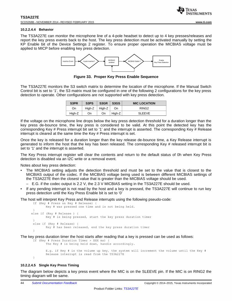
MICBIAS
enabled
Enable
Key Press DetectionMICBIAS Stable ?4-pole inserted ?Insertion Event
TS3A227ESCDS358B –NOVEMBER 2014–REVISED FEBRUARY 2015 www.ti.com
10.2.2.4.4 Behavior
The TS3A227E can monitor the microphone line of a 4-pole headset to detect up to 4 key presses/releases andreport the key press events back to the host. The key press detection must be activated manually by setting theKP Enable bit of the Device Settings 2 register. To ensure proper operation the MICBIAS voltage must beapplied to MICP before enabling key press detection.
Figure 33. Proper Key Press Enable Sequence
The TS3A227E monitors the S3 switch matrix to determine the location of the microphone. If the Manual SwitchControl bit is set to ‘1’, the S3 matrix must be configured in one of the following 2 configurations for the key pressdetection to operate. Other configurations are not supported with key press detection.
S3PR S3PS S3GR S3GS MIC LOCATIONOn High-Z High-Z On RING2
High-Z On On High-Z SLEEVE
If the voltage on the microphone line drops below the key press detection threshold for a duration longer than thekey press de-bounce time, the key press is considered to be valid. At this point the detected key has thecorresponding Key # Press interrupt bit set to ‘1’ and the interrupt is asserted. The corresponding Key # Releaseinterrupt is cleared at the same time the Key # Press interrupt is set.
Once the key is released for a duration longer than the key release de-bounce time, a Key Release interrupt isgenerated to inform the host that the key has been released. The corresponding Key # released interrupt bit isset to ‘1’ and the interrupt is asserted.
The Key Press interrupt register will clear the contents and return to the default status of 0h when Key Pressdetection is disabled via an I2C write or a removal event.
Notes about key press detection:• The MICBIAS setting adjusts the detection threshold and must be set to the value that is closest to the
MICBIAS output of the codec. If the MICBIAS voltage being used is between different MICBIAS settings ofthe TS3A227E then the closest value that is greater than the MICBIAS voltage should be used.– E.G. if the codec output is 2.2 V, the 2.3 V MICBIAS setting in the TS3A227E should be used.
• If any pending interrupt is not read by the host and a key is pressed, the TS3A227E will continue to run keypress detection until the Key Press Enable bit is set to ‘0’
The host will interpret Key Press and Release interrupts using the following pseudo-code:If (Key # Press && Key # Release) {
Key # was pressed one time and is not being held.}
else if (Key # Release ) {Key # is being pressed, start the key press duration timer
}else if (Key # Release) {
Key # has been released, end the key press duration timer}
The key press duration timer the host starts after reading that a key is pressed can be used as follows:If (Key # Press Duration Timer > XXX ms) {
The Key # is being held down, handle accordingly.
E.g. if Key # is the volume up key, the system will increment the volume until the Key #Release interrupt is read from the TS3A227E
}
10.2.2.4.5 Single Key Press Timing
The diagram below depicts a key press event where the MIC is on the SLEEVE pin. If the MIC is on RING2 thetiming diagram will be same.
44 Submit Documentation Feedback Copyright © 2014–2015, Texas Instruments Incorporated
Product Folder Links: TS3A227E
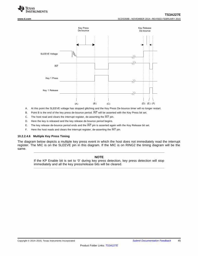
SLEEVE Voltage
INT
Key PressDe-bounce
(A)
Key Release
De-bounce
(C)
Key 1 Press
Key 1 Release
(D) (E) (F)(B)
TS3A227Ewww.ti.com SCDS358B –NOVEMBER 2014–REVISED FEBRUARY 2015
A. At this point the SLEEVE voltage has stopped glitching and the Key Press De-bounce timer will no longer restart.B. Point B is the end of the key press de-bounce period. INT will be asserted with the Key Press bit set.C. The host read and clears the interrupt register, de-asserting the INT pin.D. Here the key is released and the key release de-bounce period begins.E. The key release de-bounce period ends and the INT pin is asserted again with the Key Release bit set.F. Here the host reads and clears the interrupt register, de-asserting the INT pin.
10.2.2.4.6 Multiple Key Press Timing
The diagram below depicts a multiple key press event in which the host does not immediately read the interruptregister. The MIC is on the SLEEVE pin in this diagram. If the MIC is on RING2 the timing diagram will be thesame.
NOTEIf the KP Enable bit is set to ‘0’ during key press detection, key press detection will stopimmediately and all the key press/release bits will be cleared.
Copyright © 2014–2015, Texas Instruments Incorporated Submit Documentation Feedback 45
Product Folder Links: TS3A227E
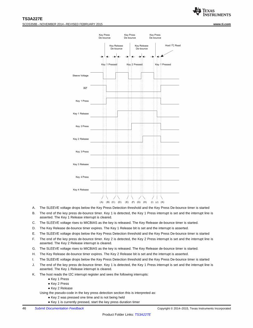
Key 1 Pressed
Sleeve Voltage
INT
Key 1 Press
Key 1 Release
Key 2 Press
Key 2 Release
(A) (B) (C) (D) (E) (F) (G) (H) (I) (J) (K)
Key 2 Pressed Key 1 Pressed
Key 3 Press
Key 3 Release
Key 4 Press
Key 4 Release
Key Press
De-bounce
Key Press
De-bounce
Key Press
De-bounce
Key Release
De-bounce
Key Release
De-bounce
Host I 2C Read
TS3A227ESCDS358B –NOVEMBER 2014–REVISED FEBRUARY 2015 www.ti.com
A. The SLEEVE voltage drops below the Key Press Detection threshold and the Key Press De-bounce timer is startedB. The end of the key press de-bounce timer. Key 1 is detected, the Key 1 Press interrupt is set and the interrupt line is
asserted. The Key 1 Release interrupt is cleared.C. The SLEEVE voltage rises to MICBIAS as the key is released. The Key Release de-bounce timer is started.D. The Key Release de-bounce timer expires. The Key 1 Release bit is set and the interrupt is asserted.E. The SLEEVE voltage drops below the Key Press Detection threshold and the Key Press De-bounce timer is startedF. The end of the key press de-bounce timer. Key 2 is detected, the Key 2 Press interrupt is set and the interrupt line is
asserted. The Key 2 Release interrupt is cleared.G. The SLEEVE voltage rises to MICBIAS as the key is released. The Key Release de-bounce timer is started.H. The Key Release de-bounce timer expires. The Key 2 Release bit is set and the interrupt is asserted.I. The SLEEVE voltage drops below the Key Press Detection threshold and the Key Press De-bounce timer is startedJ. The end of the key press de-bounce timer. Key 1 is detected, the Key 1 Press interrupt is set and the interrupt line is
asserted. The Key 1 Release interrupt is cleared.K. The host reads the I2C interrupt register and sees the following interrupts:
mmm● Key 1 Pressmmm● Key 2 Pressmmm● Key 2 ReleaseUsing the pseudo-code in the key press detection section this is interpreted as:mmm● Key 2 was pressed one time and is not being heldmmm● Key 1 is currently pressed, start the key press duration timer
46 Submit Documentation Feedback Copyright © 2014–2015, Texas Instruments Incorporated
Product Folder Links: TS3A227E
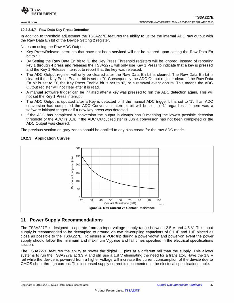
Contact Resistance (m:)
Max
Cur
rent
Sup
porte
d (m
A)
20 30 40 50 60 70 80 90 1000
50
100
150
200
250
300
D001
TS3A227Ewww.ti.com SCDS358B –NOVEMBER 2014–REVISED FEBRUARY 2015
10.2.2.4.7 Raw Data Key Press Detection
In addition to threshold adjustment the TS3A227E features the ability to utilize the internal ADC raw output withthe Raw Data En bit of the Device Setting 2 register.
Notes on using the Raw ADC Output:• Key Press/Release interrupts that have not been serviced will not be cleared upon setting the Raw Data En
bit to ‘1’.• By Setting the Raw Data En bit to ‘1’ the Key Press Threshold registers will be ignored. Instead of reporting
key 1 through 4 press and releases the TS3A227E will only use Key 1 Press to indicate that a key is pressedand the Key 1 Release interrupt to report that the key was released.
• The ADC Output register will only be cleared after the Raw Data En bit is cleared. The Raw Data En bit iscleared if the Key Press Enable bit is set to ‘0’. Consequently the ADC Output register clears if the Raw DataEn bit is set to ‘0’, the Key Press Enable bit is set to ‘0’, or a removal event occurs. This means the ADCOutput register will not clear after it is read.
• A manual software trigger can be initiated after a key was pressed to run the ADC detection again. This willnot set the Key 1 Press interrupt.
• The ADC Output is updated after a Key is detected or if the manual ADC trigger bit is set to ‘1’. If an ADCconversion has completed the ADC Conversion interrupt bit will be set to ‘1’ regardless if there was asoftware initiated trigger or if a new key press was detected.
• If the ADC has completed a conversion the output is always non 0 meaning the lowest possible detectionthreshold of the ADC is 01h. If the ADC Output register is 00h a conversion has not been completed or theADC Output was cleared.
The previous section on gray zones should be applied to any bins create for the raw ADC mode.
10.2.3 Application Curves
Figure 34. Max Current vs Contact Resistance
11 Power Supply RecommendationsThe TS3A227E is designed to operate from an input voltage supply range between 2.5 V and 4.5 V. This inputsupply is recommended to be decoupled to ground via two de-coupling capacitors of 0.1µF and 1µF placed asclose as possible to the TS3A227E. To ensure a POR trip during a power-down and power-on event the powersupply should follow the minimum and maximum VDD rise and fall times specified in the electrical specificationssection.
The TS3A227E features the ability to power the digital IO pins at a different rail than the supply. This allowssystems to run the TS3A227E at 3.3 V and still use a 1.8 V eliminating the need for a translator. Have the 1.8 Vrail while the device is powered from a higher voltage will increase the current consumption of the device due toCMOS shoot through current. This increased supply current is documented in the electrical specifications table.
Copyright © 2014–2015, Texas Instruments Incorporated Submit Documentation Feedback 47
Product Folder Links: TS3A227E
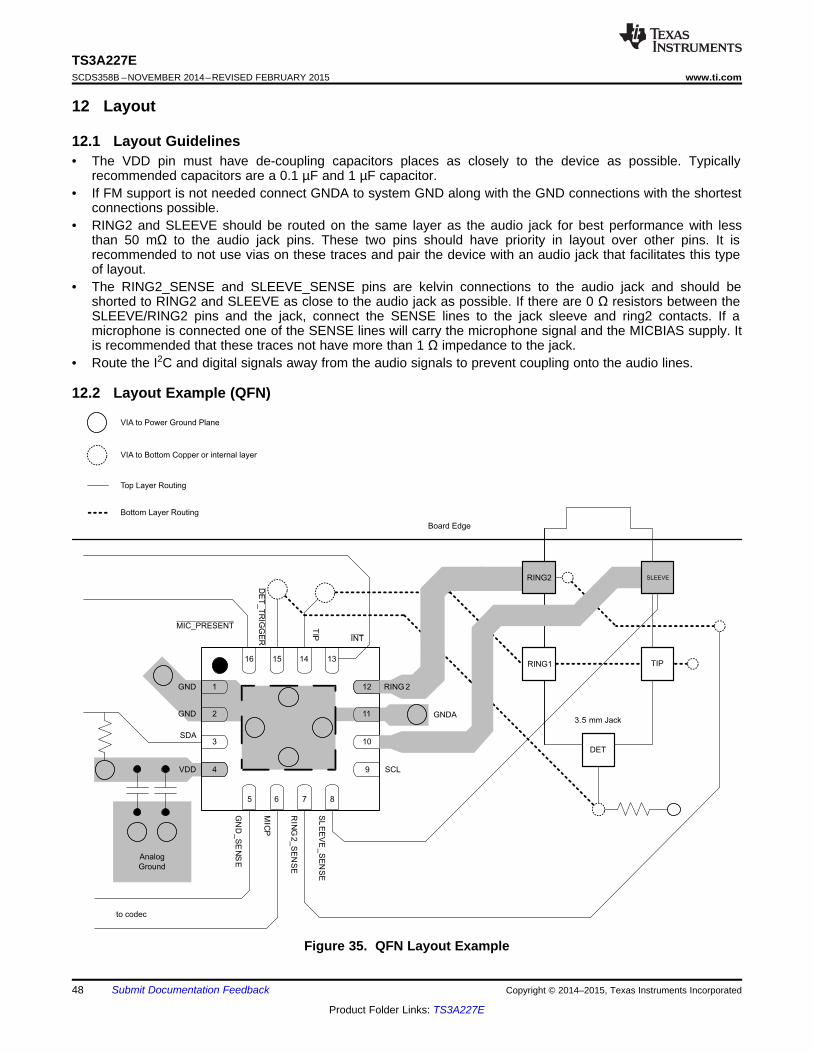
MIC_PRESENT
INT
GND
TIP
GND
SDA
VDD
GN
D_S
EN
SE
MIC
P
RIN
G2_S
EN
SE
SL
EE
VE
_S
EN
SE
SLEEVE
SCL
16 15 14 13
5 6 7 8
1
2
3
4
12
11
10
9
DET
TIPRING1
3.5 mm Jack
RING 2
GNDA
Analog
Ground
VIA to Power Ground Plane
VIA to Bottom Copper or internal layer
Board Edge
to codec
Top Layer Routing
Bottom Layer Routing
RING2 SLEEVE
DE
T_
TR
IGG
ER
TS3A227ESCDS358B –NOVEMBER 2014–REVISED FEBRUARY 2015 www.ti.com
12 Layout
12.1 Layout Guidelines• The VDD pin must have de-coupling capacitors places as closely to the device as possible. Typically
recommended capacitors are a 0.1 µF and 1 µF capacitor.• If FM support is not needed connect GNDA to system GND along with the GND connections with the shortest
connections possible.• RING2 and SLEEVE should be routed on the same layer as the audio jack for best performance with less
than 50 mΩ to the audio jack pins. These two pins should have priority in layout over other pins. It isrecommended to not use vias on these traces and pair the device with an audio jack that facilitates this typeof layout.
• The RING2_SENSE and SLEEVE_SENSE pins are kelvin connections to the audio jack and should beshorted to RING2 and SLEEVE as close to the audio jack as possible. If there are 0 Ω resistors between theSLEEVE/RING2 pins and the jack, connect the SENSE lines to the jack sleeve and ring2 contacts. If amicrophone is connected one of the SENSE lines will carry the microphone signal and the MICBIAS supply. Itis recommended that these traces not have more than 1 Ω impedance to the jack.
• Route the I2C and digital signals away from the audio signals to prevent coupling onto the audio lines.
12.2 Layout Example (QFN)
Figure 35. QFN Layout Example
48 Submit Documentation Feedback Copyright © 2014–2015, Texas Instruments Incorporated
Product Folder Links: TS3A227E
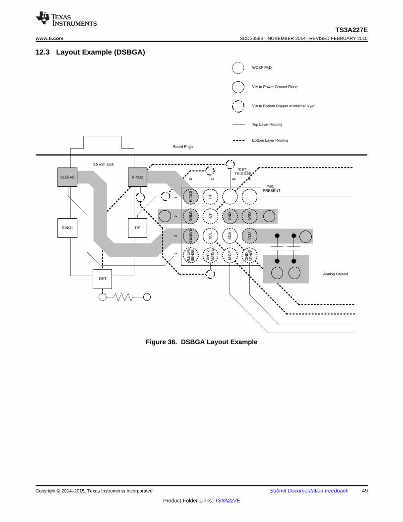
DET
RING1
3.5 mm Jack
Analog Ground
VIA to Power Ground Plane
VIA to Bottom Copper or internal layer
Board Edge
Top Layer Routing
Bottom Layer Routing
41
D C B A
2
RIN
G2
/MIC_PRESENT
/DET_TRIGGER
SD
AG
ND
GN
DV
DD
GN
DA
SLEEVE
SLE
EV
E
TIP
3RING2
SLE
EV
ES
EN
SE
TIP
RIN
G2_
SE
NS
ES
CL
WCSP PAD
MIC
P
GN
D_
SE
NS
E
INT
TS3A227Ewww.ti.com SCDS358B –NOVEMBER 2014–REVISED FEBRUARY 2015
12.3 Layout Example (DSBGA)
Figure 36. DSBGA Layout Example
Copyright © 2014–2015, Texas Instruments Incorporated Submit Documentation Feedback 49
Product Folder Links: TS3A227E
TS3A227ESCDS358B –NOVEMBER 2014–REVISED FEBRUARY 2015 www.ti.com
13 Device and Documentation Support
13.1 TrademarksAll trademarks are the property of their respective owners.
13.2 Electrostatic Discharge CautionThese devices have limited built-in ESD protection. The leads should be shorted together or the device placed in conductive foamduring storage or handling to prevent electrostatic damage to the MOS gates.
13.3 GlossarySLYZ022 — TI Glossary.
This glossary lists and explains terms, acronyms, and definitions.
14 Mechanical, Packaging, and Orderable InformationThe following pages include mechanical, packaging, and orderable information. This information is the mostcurrent data available for the designated devices. This data is subject to change without notice and revision ofthis document. For browser-based versions of this data sheet, refer to the left-hand navigation.
50 Submit Documentation Feedback Copyright © 2014–2015, Texas Instruments Incorporated
Product Folder Links: TS3A227E
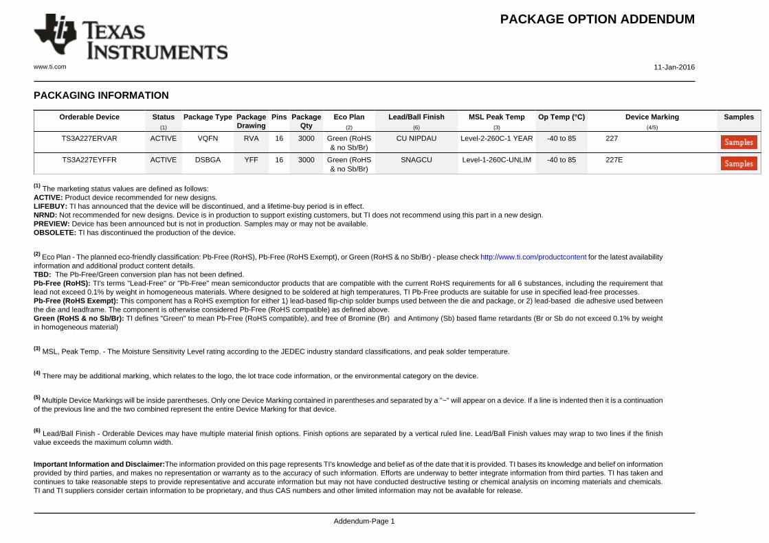
PACKAGE OPTION ADDENDUM
www.ti.com 11-Jan-2016
Addendum-Page 1
PACKAGING INFORMATION
Orderable Device Status(1)
Package Type PackageDrawing
Pins PackageQty
Eco Plan(2)
Lead/Ball Finish(6)
MSL Peak Temp(3)
Op Temp (°C) Device Marking(4/5)
Samples
TS3A227ERVAR ACTIVE VQFN RVA 16 3000 Green (RoHS& no Sb/Br)
CU NIPDAU Level-2-260C-1 YEAR -40 to 85 227
TS3A227EYFFR ACTIVE DSBGA YFF 16 3000 Green (RoHS& no Sb/Br)
SNAGCU Level-1-260C-UNLIM -40 to 85 227E
(1) The marketing status values are defined as follows:ACTIVE: Product device recommended for new designs.LIFEBUY: TI has announced that the device will be discontinued, and a lifetime-buy period is in effect.NRND: Not recommended for new designs. Device is in production to support existing customers, but TI does not recommend using this part in a new design.PREVIEW: Device has been announced but is not in production. Samples may or may not be available.OBSOLETE: TI has discontinued the production of the device.
(2) Eco Plan - The planned eco-friendly classification: Pb-Free (RoHS), Pb-Free (RoHS Exempt), or Green (RoHS & no Sb/Br) - please check http://www.ti.com/productcontent for the latest availabilityinformation and additional product content details.TBD: The Pb-Free/Green conversion plan has not been defined.Pb-Free (RoHS): TI's terms "Lead-Free" or "Pb-Free" mean semiconductor products that are compatible with the current RoHS requirements for all 6 substances, including the requirement thatlead not exceed 0.1% by weight in homogeneous materials. Where designed to be soldered at high temperatures, TI Pb-Free products are suitable for use in specified lead-free processes.Pb-Free (RoHS Exempt): This component has a RoHS exemption for either 1) lead-based flip-chip solder bumps used between the die and package, or 2) lead-based die adhesive used betweenthe die and leadframe. The component is otherwise considered Pb-Free (RoHS compatible) as defined above.Green (RoHS & no Sb/Br): TI defines "Green" to mean Pb-Free (RoHS compatible), and free of Bromine (Br) and Antimony (Sb) based flame retardants (Br or Sb do not exceed 0.1% by weightin homogeneous material)
(3) MSL, Peak Temp. - The Moisture Sensitivity Level rating according to the JEDEC industry standard classifications, and peak solder temperature.
(4) There may be additional marking, which relates to the logo, the lot trace code information, or the environmental category on the device.
(5) Multiple Device Markings will be inside parentheses. Only one Device Marking contained in parentheses and separated by a "~" will appear on a device. If a line is indented then it is a continuationof the previous line and the two combined represent the entire Device Marking for that device.
(6) Lead/Ball Finish - Orderable Devices may have multiple material finish options. Finish options are separated by a vertical ruled line. Lead/Ball Finish values may wrap to two lines if the finishvalue exceeds the maximum column width.
Important Information and Disclaimer:The information provided on this page represents TI's knowledge and belief as of the date that it is provided. TI bases its knowledge and belief on informationprovided by third parties, and makes no representation or warranty as to the accuracy of such information. Efforts are underway to better integrate information from third parties. TI has taken andcontinues to take reasonable steps to provide representative and accurate information but may not have conducted destructive testing or chemical analysis on incoming materials and chemicals.TI and TI suppliers consider certain information to be proprietary, and thus CAS numbers and other limited information may not be available for release.

PACKAGE OPTION ADDENDUM
www.ti.com 11-Jan-2016
Addendum-Page 2
In no event shall TI's liability arising out of such information exceed the total purchase price of the TI part(s) at issue in this document sold by TI to Customer on an annual basis.
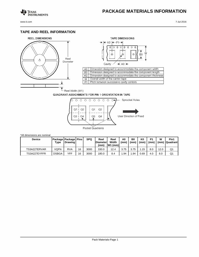
TAPE AND REEL INFORMATION
*All dimensions are nominal
Device PackageType
PackageDrawing
Pins SPQ ReelDiameter
(mm)
ReelWidth
W1 (mm)
A0(mm)
B0(mm)
K0(mm)
P1(mm)
W(mm)
Pin1Quadrant
TS3A227ERVAR VQFN RVA 16 3000 330.0 12.4 3.75 3.75 1.15 8.0 12.0 Q1
TS3A227EYFFR DSBGA YFF 16 3000 180.0 8.4 1.94 1.94 0.69 4.0 8.0 Q1
PACKAGE MATERIALS INFORMATION
www.ti.com 7-Jul-2016
Pack Materials-Page 1
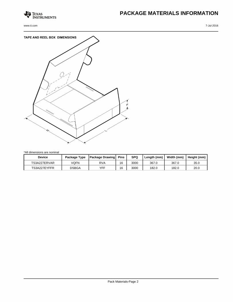
*All dimensions are nominal
Device Package Type Package Drawing Pins SPQ Length (mm) Width (mm) Height (mm)
TS3A227ERVAR VQFN RVA 16 3000 367.0 367.0 35.0
TS3A227EYFFR DSBGA YFF 16 3000 182.0 182.0 20.0
PACKAGE MATERIALS INFORMATION
www.ti.com 7-Jul-2016
Pack Materials-Page 2
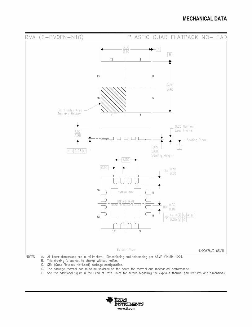
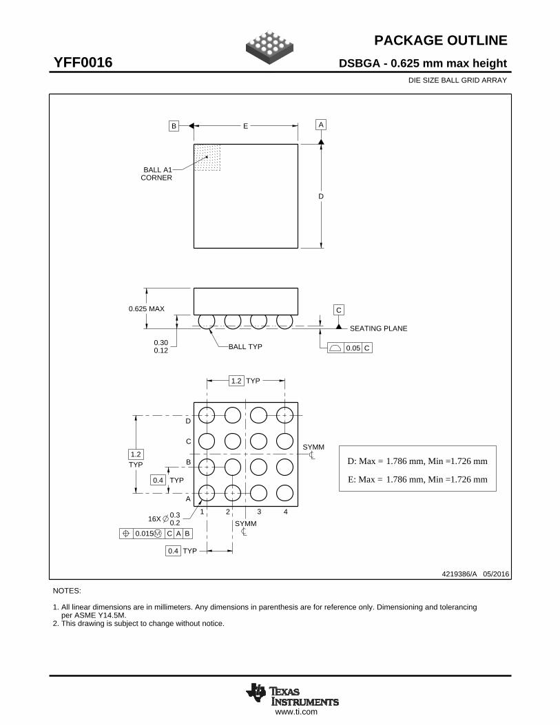
www.ti.com
PACKAGE OUTLINE
C0.625 MAX
0.300.12
1.2TYP
1.2 TYP
0.4 TYP
0.4 TYP
16X 0.30.2
B E A
D
DSBGA - 0.625 mm max heightYFF0016DIE SIZE BALL GRID ARRAY
4219386/A 05/2016
NOTES: 1. All linear dimensions are in millimeters. Any dimensions in parenthesis are for reference only. Dimensioning and tolerancing per ASME Y14.5M.2. This drawing is subject to change without notice.
BALL A1CORNER
SEATING PLANE
BALL TYP 0.05 C
B
1 2 3
0.015 C A B
SYMM
SYMM
A
C
D
4
SCALE 8.000
D: Max =
E: Max =
1.786 mm, Min =
1.786 mm, Min =
1.726 mm
1.726 mm
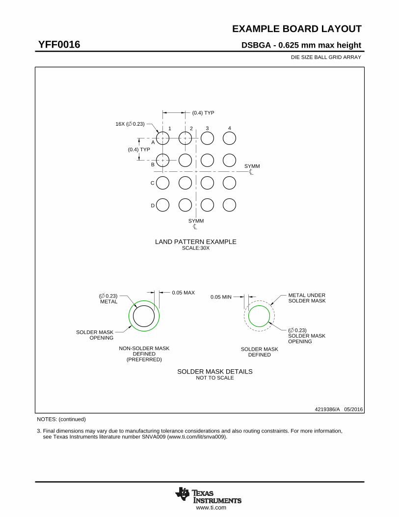
www.ti.com
EXAMPLE BOARD LAYOUT
16X ( 0.23)
(0.4) TYP
(0.4) TYP
( 0.23)METAL
0.05 MAX
SOLDER MASKOPENING
METAL UNDERSOLDER MASK
( 0.23)SOLDER MASKOPENING
0.05 MIN
DSBGA - 0.625 mm max heightYFF0016DIE SIZE BALL GRID ARRAY
4219386/A 05/2016
NOTES: (continued) 3. Final dimensions may vary due to manufacturing tolerance considerations and also routing constraints. For more information, see Texas Instruments literature number SNVA009 (www.ti.com/lit/snva009).
SYMM
SYMM
LAND PATTERN EXAMPLESCALE:30X
C
1 2 3
A
B
D
4
NON-SOLDER MASKDEFINED
(PREFERRED)
SOLDER MASK DETAILSNOT TO SCALE
SOLDER MASKDEFINED
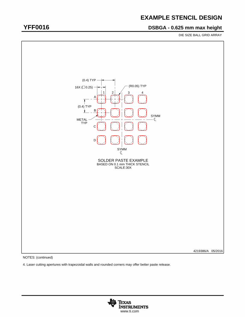
www.ti.com
EXAMPLE STENCIL DESIGN
(0.4) TYP
(0.4) TYP
16X ( 0.25) (R0.05) TYP
METALTYP
DSBGA - 0.625 mm max heightYFF0016DIE SIZE BALL GRID ARRAY
4219386/A 05/2016
NOTES: (continued) 4. Laser cutting apertures with trapezoidal walls and rounded corners may offer better paste release.
SYMM
SYMM
C
1 2 3A
B
D
SOLDER PASTE EXAMPLEBASED ON 0.1 mm THICK STENCIL
SCALE:30X
4

IMPORTANT NOTICE
Texas Instruments Incorporated (TI) reserves the right to make corrections, enhancements, improvements and other changes to itssemiconductor products and services per JESD46, latest issue, and to discontinue any product or service per JESD48, latest issue. Buyersshould obtain the latest relevant information before placing orders and should verify that such information is current and complete.TI’s published terms of sale for semiconductor products (http://www.ti.com/sc/docs/stdterms.htm) apply to the sale of packaged integratedcircuit products that TI has qualified and released to market. Additional terms may apply to the use or sale of other types of TI products andservices.Reproduction of significant portions of TI information in TI data sheets is permissible only if reproduction is without alteration and isaccompanied by all associated warranties, conditions, limitations, and notices. TI is not responsible or liable for such reproduceddocumentation. Information of third parties may be subject to additional restrictions. Resale of TI products or services with statementsdifferent from or beyond the parameters stated by TI for that product or service voids all express and any implied warranties for theassociated TI product or service and is an unfair and deceptive business practice. TI is not responsible or liable for any such statements.Buyers and others who are developing systems that incorporate TI products (collectively, “Designers”) understand and agree that Designersremain responsible for using their independent analysis, evaluation and judgment in designing their applications and that Designers havefull and exclusive responsibility to assure the safety of Designers' applications and compliance of their applications (and of all TI productsused in or for Designers’ applications) with all applicable regulations, laws and other applicable requirements. Designer represents that, withrespect to their applications, Designer has all the necessary expertise to create and implement safeguards that (1) anticipate dangerousconsequences of failures, (2) monitor failures and their consequences, and (3) lessen the likelihood of failures that might cause harm andtake appropriate actions. Designer agrees that prior to using or distributing any applications that include TI products, Designer willthoroughly test such applications and the functionality of such TI products as used in such applications.TI’s provision of technical, application or other design advice, quality characterization, reliability data or other services or information,including, but not limited to, reference designs and materials relating to evaluation modules, (collectively, “TI Resources”) are intended toassist designers who are developing applications that incorporate TI products; by downloading, accessing or using TI Resources in anyway, Designer (individually or, if Designer is acting on behalf of a company, Designer’s company) agrees to use any particular TI Resourcesolely for this purpose and subject to the terms of this Notice.TI’s provision of TI Resources does not expand or otherwise alter TI’s applicable published warranties or warranty disclaimers for TIproducts, and no additional obligations or liabilities arise from TI providing such TI Resources. TI reserves the right to make corrections,enhancements, improvements and other changes to its TI Resources. TI has not conducted any testing other than that specificallydescribed in the published documentation for a particular TI Resource.Designer is authorized to use, copy and modify any individual TI Resource only in connection with the development of applications thatinclude the TI product(s) identified in such TI Resource. NO OTHER LICENSE, EXPRESS OR IMPLIED, BY ESTOPPEL OR OTHERWISETO ANY OTHER TI INTELLECTUAL PROPERTY RIGHT, AND NO LICENSE TO ANY TECHNOLOGY OR INTELLECTUAL PROPERTYRIGHT OF TI OR ANY THIRD PARTY IS GRANTED HEREIN, including but not limited to any patent right, copyright, mask work right, orother intellectual property right relating to any combination, machine, or process in which TI products or services are used. Informationregarding or referencing third-party products or services does not constitute a license to use such products or services, or a warranty orendorsement thereof. Use of TI Resources may require a license from a third party under the patents or other intellectual property of thethird party, or a license from TI under the patents or other intellectual property of TI.TI RESOURCES ARE PROVIDED “AS IS” AND WITH ALL FAULTS. TI DISCLAIMS ALL OTHER WARRANTIES ORREPRESENTATIONS, EXPRESS OR IMPLIED, REGARDING RESOURCES OR USE THEREOF, INCLUDING BUT NOT LIMITED TOACCURACY OR COMPLETENESS, TITLE, ANY EPIDEMIC FAILURE WARRANTY AND ANY IMPLIED WARRANTIES OFMERCHANTABILITY, FITNESS FOR A PARTICULAR PURPOSE, AND NON-INFRINGEMENT OF ANY THIRD PARTY INTELLECTUALPROPERTY RIGHTS. TI SHALL NOT BE LIABLE FOR AND SHALL NOT DEFEND OR INDEMNIFY DESIGNER AGAINST ANY CLAIM,INCLUDING BUT NOT LIMITED TO ANY INFRINGEMENT CLAIM THAT RELATES TO OR IS BASED ON ANY COMBINATION OFPRODUCTS EVEN IF DESCRIBED IN TI RESOURCES OR OTHERWISE. IN NO EVENT SHALL TI BE LIABLE FOR ANY ACTUAL,DIRECT, SPECIAL, COLLATERAL, INDIRECT, PUNITIVE, INCIDENTAL, CONSEQUENTIAL OR EXEMPLARY DAMAGES INCONNECTION WITH OR ARISING OUT OF TI RESOURCES OR USE THEREOF, AND REGARDLESS OF WHETHER TI HAS BEENADVISED OF THE POSSIBILITY OF SUCH DAMAGES.Unless TI has explicitly designated an individual product as meeting the requirements of a particular industry standard (e.g., ISO/TS 16949and ISO 26262), TI is not responsible for any failure to meet such industry standard requirements.Where TI specifically promotes products as facilitating functional safety or as compliant with industry functional safety standards, suchproducts are intended to help enable customers to design and create their own applications that meet applicable functional safety standardsand requirements. Using products in an application does not by itself establish any safety features in the application. Designers mustensure compliance with safety-related requirements and standards applicable to their applications. Designer may not use any TI products inlife-critical medical equipment unless authorized officers of the parties have executed a special contract specifically governing such use.Life-critical medical equipment is medical equipment where failure of such equipment would cause serious bodily injury or death (e.g., lifesupport, pacemakers, defibrillators, heart pumps, neurostimulators, and implantables). Such equipment includes, without limitation, allmedical devices identified by the U.S. Food and Drug Administration as Class III devices and equivalent classifications outside the U.S.TI may expressly designate certain products as completing a particular qualification (e.g., Q100, Military Grade, or Enhanced Product).Designers agree that it has the necessary expertise to select the product with the appropriate qualification designation for their applicationsand that proper product selection is at Designers’ own risk. Designers are solely responsible for compliance with all legal and regulatoryrequirements in connection with such selection.Designer will fully indemnify TI and its representatives against any damages, costs, losses, and/or liabilities arising out of Designer’s non-compliance with the terms and provisions of this Notice.
Mailing Address: Texas Instruments, Post Office Box 655303, Dallas, Texas 75265Copyright © 2017, Texas Instruments Incorporated


![F3JR MB R20 1211[31731]ncandelier.free.fr/asus/ASUS_F3JR_R20.pdfH_D#50 H_TMS H_TDO H_TCK H_TRST# H_PREQ# +VCCP +VCCP +VCCP +VCCP GND GND GND GND GND GND GND TPC26T 1 T1 R8 1 2 56Ohm](https://img.pdfslide.us/doc/110x75/5faf0ab01979a324157ec2b6/f3jr-mb-r20-121131731-hd50-htms-htdo-htck-htrst-hpreq-vccp-vccp-vccp.jpg)


![Wireless Starter Kit Mainboard - Silicon Labs · vcom_enable pti0[0..2] vmcu gnd gnd gnd gnd vmcu vrf 5v 3v3 gnd vrf gnd gnd gnd gnd gnd usb_vbus usb_vreg usb_vbus 5v 5v_dbg …](https://img.pdfslide.us/doc/110x75/5ac0fbea7f8b9a4e7c8c7c14/wireless-starter-kit-mainboard-silicon-labs-pti002-vmcu-gnd-gnd-gnd-gnd-vmcu.jpg)