Embed Size (px)
Citation preview
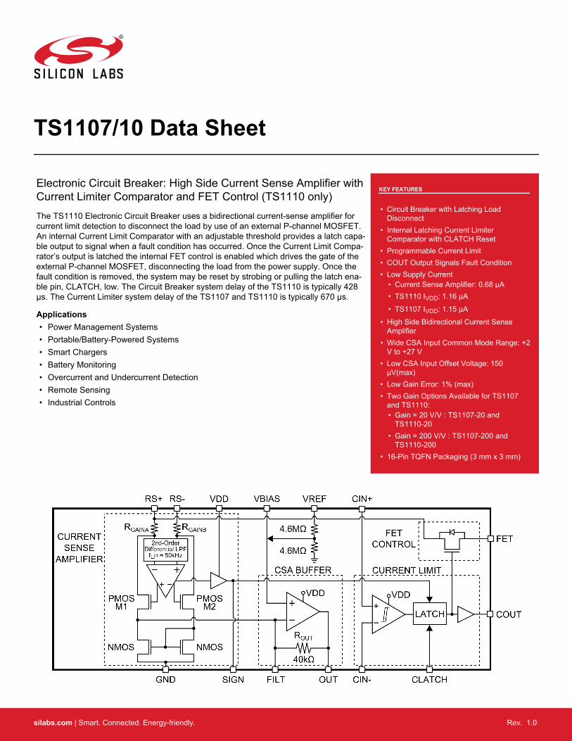
TS1107/10 Data Sheet
Electronic Circuit Breaker: High Side Current Sense Amplifier withCurrent Limiter Comparator and FET Control (TS1110 only)The TS1110 Electronic Circuit Breaker uses a bidirectional current-sense amplifier forcurrent limit detection to disconnect the load by use of an external P-channel MOSFET.An internal Current Limit Comparator with an adjustable threshold provides a latch capa-ble output to signal when a fault condition has occurred. Once the Current Limit Compa-rator’s output is latched the internal FET control is enabled which drives the gate of theexternal P-channel MOSFET, disconnecting the load from the power supply. Once thefault condition is removed, the system may be reset by strobing or pulling the latch ena-ble pin, CLATCH, low. The Circuit Breaker system delay of the TS1110 is typically 428µs. The Current Limiter system delay of the TS1107 and TS1110 is typically 670 µs.
Applications• Power Management Systems• Portable/Battery-Powered Systems• Smart Chargers• Battery Monitoring• Overcurrent and Undercurrent Detection• Remote Sensing• Industrial Controls
KEY FEATURES
• Circuit Breaker with Latching LoadDisconnect
• Internal Latching Current LimiterComparator with CLATCH Reset
• Programmable Current Limit• COUT Output Signals Fault Condition• Low Supply Current
• Current Sense Amplifier: 0.68 µA• TS1110 IVDD: 1.16 µA
• TS1107 IVDD: 1.15 µA
• High Side Bidirectional Current SenseAmplifier
• Wide CSA Input Common Mode Range: +2V to +27 V
• Low CSA Input Offset Voltage: 150µV(max)
• Low Gain Error: 1% (max)• Two Gain Options Available for TS1107
and TS1110:• Gain = 20 V/V : TS1107-20 and
TS1110-20• Gain = 200 V/V : TS1107-200 and
TS1110-200• 16-Pin TQFN Packaging (3 mm x 3 mm)
silabs.com | Smart. Connected. Energy-friendly. Rev. 1.0

1. Ordering Information
Table 1.1. Ordering Part Numbers
Ordering Part Number Description FET Control Gain V/V
TS1107-20ITQ1633 Electronic Circuit Breaker: High Side Current Sense Amplifier with CurrentLimiter Comparator
No 20
TS1107-200ITQ1633 Electronic Circuit Breaker: High Side Current Sense Amplifier with CurrentLimiter Comparator
No 200
TS1110-20ITQ1633 Electronic Circuit Breaker: High Side Current Sense Amplifier with CurrentLimiter Comparator and FET Control
Yes 20
TS1110-200ITQ1633 Electronic Circuit Breaker: High Side Current Sense Amplifier with CurrentLimiter Comparator and FET Control
Yes 200
Note: Adding the suffix “T” to the part number (e.g. TS1107-200ITQ1633T) denotes tape and reel.
TS1107/10 Data SheetOrdering Information
silabs.com | Smart. Connected. Energy-friendly. Rev. 1.0 | 1

2. System Overview
2.1 Functional Block Diagrams
Figure 2.1. TS1110 Current Limit with FET Control Block Diagram
Figure 2.2. TS1107 Current Limit Block Diagram
TS1107/10 Data SheetSystem Overview
silabs.com | Smart. Connected. Energy-friendly. Rev. 1.0 | 2

2.2 Current Sense Amplifier + Output Buffer
The internal configuration of the TS1107/10 bidirectional current-sense amplifier is a variation of the TS1101 bidirectional current-senseamplifier. The TS1107/10 current-sense amplifier is configured for fully differential input/output operation.
Referring to the block diagram, the inputs of the TS1107/10’s differential input/output amplifier are connected to RS+ and RS– acrossan external RSENSE resistor that is used to measure current. At the non-inverting input of the current-sense amplifier, the applied volt-age difference in voltage between RS+ and RS– is ILOAD x RSENSE. Since the RS– terminal is the non-inverting input of the internal op-amp, the current-sense op-amp action drives PMOS[1/2] to drive current across RGAIN[A/B] to equalize voltage at its inputs.
Thus, since the M1 PMOS source is connected to the inverting input of the internal op-amp and since the voltage drop across RGAINA isthe same as the external VSENSE, the M1 PMOS drain-source current is equal to:
IDS (M 1) =VSENSERGAINA
or
IDS (M 1) =ILOAD × RSENSE
RGAINA
The drain terminal of the M1 PMOS is connected to the transimpedance amplifier’s gain resistor, ROUT, via the inverting terminal. Thenon-inverting terminal of the transimpedance amplifier is internally connected to VBIAS, therefore the output voltage of the TS1107/10at the OUT terminal is:
VOUT = VBIAS − ILOAD × RSENSE ×ROUTRGAINA
When the voltage at the RS– terminal is greater than the voltage at the RS+ terminal, the external VSENSE voltage drop is impressedupon RGAINB. The voltage drop across RGAINB is then converted into a current by the M2 PMOS. The M2 PMOS drain-source current isthe input current for the NMOS current mirror which is matched with a 1-to-1 ratio. The transimpedance amplifier sources the M2 PMOSdrain-source current for the NMOS current mirror. Therefore the output voltage of the TS1107/10 at the OUT terminal is:
VOUT = VBIAS + ILOAD × RSENSE ×ROUTRGAINB
When M1 is conducting current (VRS+ > VRS–), the TS1107/10’s internal amplifier holds M2 OFF. When M2 is conducting current (VRS–> VRS+), the internal amplifier holds M1 OFF. In either case, the disabled PMOS does not contribute to the resultant output voltage.
The current-sense amplifier’s gain accuracy is therefore the ratio match of ROUT to RGAIN[A/B]. For each of the gain options available,The following table lists the values for RGAIN[A/B].
Table 2.1. Internal Gain Setting Resistors (Typical Values)
GAIN (V/V) RGAIN[A/B] (Ω) ROUT (Ω) Part Number
20 2 k 40 k TS1110-20
200 200 40 k TS1110-200
20 2 k 40 k TS1107-20
200 200 40 k TS1107-200
The TS1107/10 allows access to the inverting terminal of the transimpedance amplifier by the FILT pin, whereby a series RC filter maybe connected to reduce noise at the OUT terminal. The recommended RC filter is 4 kΩ and 0.47 μF connected in series from FILT toGND to suppress the noise. Any capacitance at the OUT terminal should be minimized for stable operation of the buffer.
TS1107/10 Data SheetSystem Overview
silabs.com | Smart. Connected. Energy-friendly. Rev. 1.0 | 3

2.3 Sign Output
The TS1107/10 SIGN output indicates the load current’s direction. The SIGN output is a logic HIGH when M1 is conducting current(VRS+ > VRS–). Alternatively, the SIGN output is a logic LOW when M2 is conducting current (VRS– > VRS+). The SIGN comparator’stransfer characteristic is illustrated in Figure 1. Unlike other current-sense amplifiers that implement an OUT/SIGN arrangement, theTS1107/10 exhibits no “dead zone” at ILOAD switchover.
Figure 2.3. TS1107/10 Sign Output Transfer Characteristic
2.4 Current Limit Comparator
The TS1107/10 provides a comparator which can be used for current limit detection. The current limit threshold can be set to detecteither positive or negative current, though it provides fastest response in the positive direction. In a typical configuration, the invertingterminal, CIN– is connected to OUT. The non-inverting terminal of the comparator, CIN+, should be supplied with an external voltage ora resistor divider from the supply voltage, which is used as the threshold voltage for the current limiter. The output of the comparator islatch capable only when the Sign Comparator is HIGH (VRS+>VRS–), and CLATCH is held HIGH. Once the comparator output (COUT)is triggered, COUT will latch HIGH and maintain the HIGH state as long as CLATCH is held HIGH. To reset COUT to the default com-parator output state, CLATCH must be held or strobed LOW.
2.5 FET Control (TS1110 Only)
A “circuit breaker” feature is supplied within the TS1110 as a FET control which drives the gate drive of an external P-channel MOS-FET. When the Current Limit Comparator’s output goes HIGH and the LATCH feature is enabled, the FET control output will latch HIGHthereby disconnecting current flow to the load by holding the gate of the external PMOS HIGH. To resume current flow to the load, theFET control must be brought low by holding or strobing CLATCH low. The output of the comparator controls the gate logic of an internalFET whereby the source is connected to the non-inverting terminal of the CSA, RS+, while the drain is fed to the FET pin. The FET pinis intended to drive the gate of an external PMOS, where the PMOS source is connected to the inverting terminal of the CSA, RS–, andthe drain is connected to the external load. FET will maintain its logic LOW state while the comparator output, COUT, is LOW. WhenCOUT is latched HIGH, the FET pin will latch to a HIGH state, thereby switching and holding the external PMOS OFF. The FET controlfeatures a Turn ON Time, tFET(ON), of 720 ns(typ) and a Turn OFF Time, tFET(OFF), of 2.9 ms(typ) when driving a 860 pF gate capaci-tance. Note that the FET Control is a pull-up only. A pull-down resistor is required from the external FET’s gate to ground to ensure theFET is normally ON.
2.6 VREF Divider
The TS1107/10 provides an internal voltage divider network to set VBIAS, eliminating the need for externally setting the voltage. TheVREF Divider is activated once the voltage applied to VREF is 0.9 V or greater. The VREF divider connects to VBIAS, where the VBIASvoltage is equal to 50% of VREF . The VREF Divider exhibits a total series resistance of 9.2 MΩ from VREF to GND.
TS1107/10 Data SheetSystem Overview
silabs.com | Smart. Connected. Energy-friendly. Rev. 1.0 | 4

2.7 Selecting a Sense Resistor
Selecting the optimal value for the external RSENSE is based on the following criteria and for each commentary follows:1. RSENSE Voltage Loss2. VOUT Swing vs. Desired VSENSE and Applied Supply Voltage at VDD3. Total ILOAD Accuracy4. Circuit Efficiency and Power Dissipation5. RSENSE Kelvin Connections
2.7.1 RSENSE Voltage Loss
For lowest IR power dissipation in RSENSE, the smallest usable resistor value for RSENSE should be selected.
2.7.2 VOUT Swing vs. Desired VSENSE and Applied Supply Voltage at VDD
Although the Current Sense Amplifier draws its power from the voltage at its RS+ and RS– terminals, the signal voltage at the OUTterminal is provided by a buffer, and is therefore bounded by the buffer’s output range. As shown in the Electrical Characteristics table,the CSA Buffer has a maximum and minimum output voltage of:
VOUT (max ) = VDD(min) − 0.2V
VOUT (min ) = 0.2V
Therefore, the full-scale sense voltage should be chosen so that the OUT voltage is neither greater nor less than the maximum andminimum output voltage defined above. To satisfy this requirement, the positive full-scale sense voltage, VSENSE(pos_max), should bechosen so that:
VSENSE (pos_max) <VBIAS − VOUT (min )
GAIN
The negative full-scale sense voltage, VSENSE(neg_min), should be chosen so that:
VSENSE (neg_min ) <VOUT (max ) − VBIAS
GAIN
For best performance, RSENSE should be chosen so that the full-scale VSENSE is less than ±75 mV.
2.7.3 Total Load Current Accuracy
In the TS1107/10’s linear region where VOUT(min) < VOUT < VOUT(max), there are two specifications related to the circuit’s accuracy: a)the TS1107/10 CSA’s input offset voltage (VOS(max) = 150 μV), b) the TS1107/10 CSA’s gain error (GE(max) = 1%). An expression forthe TS1110’s total error is given by:
VOUT = VBIAS − GAIN × (1 ± GE) × VSENSE ± (GAIN × VOS)A large value for RSENSE permits the use of smaller load currents to be measured more accurately because the effects of offset voltag-es are less significant when compared to larger VSENSE voltages. Due care though should be exercised as previously mentioned withlarge values of RSENSE.
2.7.4 Circuit Efficiency and Power Dissipation
IR loses in RSENSE can be large especially at high load currents. It is important to select the smallest, usable RSENSE value to minimizepower dissipation and to keep the physical size of RSENSE small. If the external RSENSE is allowed to dissipate significant power, thenits inherent temperature coefficient may alter its design center value, thereby reducing load current measurement accuracy. Preciselybecause the TS1107/10 CSA’s input stage was designed to exhibit a very low input offset voltage, small RSENSE values can be used toreduce power dissipation and minimize local hot spots on the pcb.
TS1107/10 Data SheetSystem Overview
silabs.com | Smart. Connected. Energy-friendly. Rev. 1.0 | 5

2.7.5 RSENSE Kelvin Connections
For optimal VSENSE accuracy in the presence of large load currents, parasitic pcb track resistance should be minimized. Kelvin-sensepcb connections between RSENSE and the TS1107/10’s RS+ and RS– terminals are strongly recommended. The drawing below illus-trates the connections between the current-sense amplifier and the current-sense resistor. The pcb layout should be balanced andsymmetrical to minimize wiring-induced errors. In addition, the pcb layout for RSENSE should include good thermal management techni-ques for optimal RSENSE power dissipation.
Figure 2.4. Making PCB Connections to RSENSE
2.7.6 RSENSE Composition
Current-shunt resistors are available in metal film, metal strip, and wire-wound constructions. Wire-wound current-shunt resistors areconstructed with wire spirally wound onto a core. As a result, these types of current shunt resistors exhibit the largest self-inductance. Inapplications where the load current contains high-frequency transients, metal film or metal strip current sense resistors are recommen-ded.
2.7.7 Internal Noise Filter
In power management and motor control applications, current-sense amplifiers are required to measure load currents accurately in thepresence of both externally-generated differential and common-mode noise. An example of differential-mode noise that can appear atthe inputs of a current-sense amplifier is high-frequency ripple. High-frequency ripple (whether injected into the circuit inductively or ca-pacitively) can produce a differential-mode voltage drop across the external current-shunt resistor, RSENSE. An example of externally-generated, common-mode noise is the high-frequency output ripple of a switching regulator that can result in common-mode noise in-jection into both inputs of a current-sense amplifier.
Even though the load current signal bandwidth is dc, the input stage of any current-sense amplifier can rectify unwanted, out-of-bandnoise that can result in an apparent error voltage at its output. Against common-mode injection noise, the current-sense amplifier’s in-ternal common-mode rejection ratio is 130 dB (typ).
To counter the effects of externally-injected noise, the TS1107/10 incorporates a 50 kHz (typ), 2nd-order differential low-pass filter asshown in the TS1107/10’s block diagram, thereby eliminating the need for an external low-pass filter which can generate errors in theoffset voltage and the gain error.
2.7.8 PC Board Layout and Power-Supply Bypassing
For optimal circuit performance, the TS1107/10 should be in very close proximity to the external current-sense resistor and the pcbtracks from RSENSE to the RS+ and the RS– input terminals of the TS1107/10 should be short and symmetric. Also recommended aresurface mount resistors and capacitors, as well as a ground plane.
TS1107/10 Data SheetSystem Overview
silabs.com | Smart. Connected. Energy-friendly. Rev. 1.0 | 6

3. Electrical Characteristics
Table 3.1. Recommended Operating Conditions1
Parameter Symbol Conditions Min Typ Max Units
System Specifications
Operating Voltage Range VDD 1.7 — 5.25 V
Common-Mode Input Range VCM VRS+, Guaranteed by CMRR 2 — 27 V
Note:1. All devices 100% production tested at TA = +25 °C. Limits over Temperature are guaranteed by design and characterization.
Table 3.2. DC Characteristics1
Parameter Symbol Conditions Min Typ Max Units
System Specifications
No Load Input Supply Current IRS+ + IRS– See Note 2 — 0.68 1.2 μA
IVDD See Note 2 TS1107 — 1.15 1.84 μA
TS1110 — 1.16 1.85 μA
Current Sense Amplifier
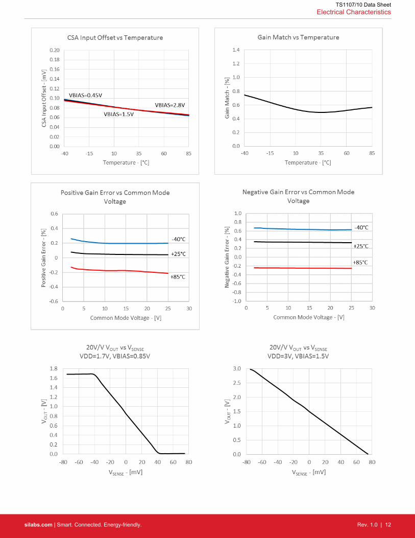
Common Mode Rejection Ratio CMRR 2 V < VRS+ < 27 V 120 130 — dB
Input Offset Voltage3 VOS TA = +25 °C — ±100 ±150 μV
–40 °C < TA < +85 °C — — ±200 μV
VOS Hysteresis4 VHYS TA = +25 °C — 10 — μV
Gain G TS1107-20, TS1110-20 — 20 — V/V
TS1107-200, TS1110-200 — 200 — V/V
Positive Gain Error5 GE+ TA = +25 °C — ±0.1 ±0.6 %
–40 °C < TA < +85 °C — — ±1 %
Negative Gain Error5 GE– TA = +25 °C — ±0.6 ±1 %
–40 °C < TA < +85 °C — — ±1.4 %
Gain Match5 GM TA = +25 °C — ±0.6 ±1 %
–40 °C < TA < +85 °C — — ±1.4 %
Transfer Resistance ROUT From FILT to OUT 28 40 52.8 kΩ
CSA Buffer
Input Bias Current IBuffer_BIAS –40 °C < TA < +85 °C — 0.3 — nA
Input referred DC Offset VBuffer_OS — — ±2.5 mV
Offset Drift TCVBuffer_OS –40 °C < TA < +85 °C — 0.6 — μV/°C
Input Common Mode Range VBuffer_CM –40 °C < TA < +85 °C 0.2 — VDD –0.2
V
TS1107/10 Data SheetElectrical Characteristics
silabs.com | Smart. Connected. Energy-friendly. Rev. 1.0 | 7

Parameter Symbol Conditions Min Typ Max Units
Output Range VOUT(min,max) IOUT = ±150 μA 0.2 — VDD –0.2
V
Sign Comparator Parameters
Output Low Voltage VSIGN_OL VDD = 1.8 V, ISINK = 35 μA — — 0.2 V
Output High Voltage VSIGN_OH VDD = 1.8 V, ISOURCE = 35 μA VDD – 0.2 — — V
Comparator
Input Bias Current ICIN–_BIAS CIN– — 0.3 — nA
Input Bias Current ICIN+_BIAS CIN+ — 0.3 — nA
Input referred DC offset VC_OS –40 °C < TA < +85 °C — — ±4 mV
Input Common Mode Range VC_CM 0.4 — VDD V
COUT Output Range VCOUT(min,max) ICOUT = ±500 μA; VDD = 1.7 V 0.4 — VDD –0.4
V
CLATCH Input Voltage CLATCHLo Low CMOS Logic Level — — 0.4 V
CLATCHHi High CMOS Logic Level VDD – 0.4 — — V
FET Control (TS1110 Only)
FET Leakage IFET_Leakage TA = +25 °C — — 4.5 nA
FET Sourcing Current IFET_Source(max) TA = +25 °C — 3.2 17.4 mA
FET Internal On Resistance RFET_ON TA = +25 °C — 487 794 Ω
VREF Divider
VREF Activation voltage VREF(min) VREF Rising edge — — 0.9 V
Resistor on VREF RVREF — 9.2 — MΩ
VBIAS VVBIAS VREF = 1 V 0.495 0.5 0.505 V
Note:1. RS+ = RS– = 3.6 V; VSENSE =(VRS+ – VRS–) = 0 V; VDD = 3 V; VBIAS = 1.5 V; CIN+ = 0.75 V; VREF = GND; CLATCH = GND;
RFET = 1 MΩ; FILT connected to 4 kΩ and 470 nF in series to GND. TA = TJ = –40 °C to +85 °C unless otherwise noted. Typicalvalues are at TA=+25 °C.
2. Extrapolated to VOUT = VFILT; IRS+ + IRS– is the total current into the RS+ and the RS– pins.3. Input offset voltage VOS is extrapolated from a VOUT(+) measurement with VSENSE set to +1 mV and a VOUT(–) measurement with
VSENSE set to –1 mV; average VOS = (VOUT(–) – VOUT(+))/(2 x GAIN).4. Amplitude of VSENSE lower or higher than VOS required to cause the comparator to switch output states.5. Gain error is calculated by applying two values for VSENSE and then calculating the error of the actual slope vs. the ideal transfer
characteristic. For GAIN = 20 V/V, the applied VSENSE for GE± is ±25 mV and ±60 mV. For GAIN = 200 V/V, the applied VSENSEfor GE± is ±2.5 mV and ±6 mV
TS1107/10 Data SheetElectrical Characteristics
silabs.com | Smart. Connected. Energy-friendly. Rev. 1.0 | 8

Table 3.3. AC Characteristics1
Parameter Symbol Conditions Min Typ Max Units
CSA Buffer
Output Settling time tOUT_s 1% Final value,VOUT = 1.3 V
Gain = 20 V/V — 1.35 — msec
Sign Comparator
Propagation Delay tSIGN_PD VSENSE = ±1 mV — 3 — msec
VSENSE = ±10 mV — 0.4 — msec
Comparator
Rising Propagation Delay tC_PDR Overdrive = 10 mV, CCOUT = 15 pF — 9 — μs
Comparator Hysteresis VC_HYS CIN– falling — 20 — mV
FET Control (TS1110 Only)
FET Turn ON Time TFET(ON) See Note 2 — 0.255 — μs
Note:1. RS+ = RS– = 3.6 V, VSENSE = (VRS+ – VRS–) = 0 V, VDD = 3 V, VBIAS = 1.5 V. TA = TJ = –40 °C to +85 °C unless otherwise
noted. Typical values are at TA = +25 °C.2. Delay after comparator is triggered. Refer to FET ON Time vs. Gate Capacitance graph.
Table 3.4. Thermal Conditions
Parameter Symbol Conditions Min Typ Max Units
Operating Temperature Range TOP –40 — +85 °C
TS1107/10 Data SheetElectrical Characteristics
silabs.com | Smart. Connected. Energy-friendly. Rev. 1.0 | 9

Table 3.5. Absolute Maximum Limits
Parameter Symbol Conditions Min Typ Max Units
RS+ Voltage VRS+ –0.3 — 27 V
RS– Voltage VRS– –0.3 — 27 V
FET Voltage (TS1110 Only) VFET –0.3 — 27 V
Supply Voltage VDD –0.3 — 6 V
OUT Voltage VOUT –0.3 — 6 V
SIGN Voltage VSIGN –0.3 — 6 V
FILT Voltage VFILT –0.3 — 6 V
CLATCH Voltage VCLATCH –0.3 — 6 V
COUT Voltage VCOUT –0.3 — 6 V
VREF Voltage VVREF –0.3 — 6 V
CIN+ Voltage VCIN+ –0.3 — VDD + 0.3 V
CIN– Voltage VCIN– –0.3 — VDD + 0.3 V
VBIAS Voltage VVBIAS –0.3 — VDD + 0.3 V
RS+ to RS– Voltage VRS+ – VRS– — — 27 V
Short Circuit Duration: OUT to GND — — Continuous
Continuous Input Current (Any Pin) –20 — 20 mA
Junction Temperature — — 150 °C
Storage Temperature Range –65 — 150 °C
Lead Temperature (Soldering, 10 s) — — 300 °C
Soldering Temperature (Reflow) — — 260 °C
ESD Tolerance
Human Body Model — — 2000 V
Machine Model — — 200 V
TS1107/10 Data SheetElectrical Characteristics
silabs.com | Smart. Connected. Energy-friendly. Rev. 1.0 | 10

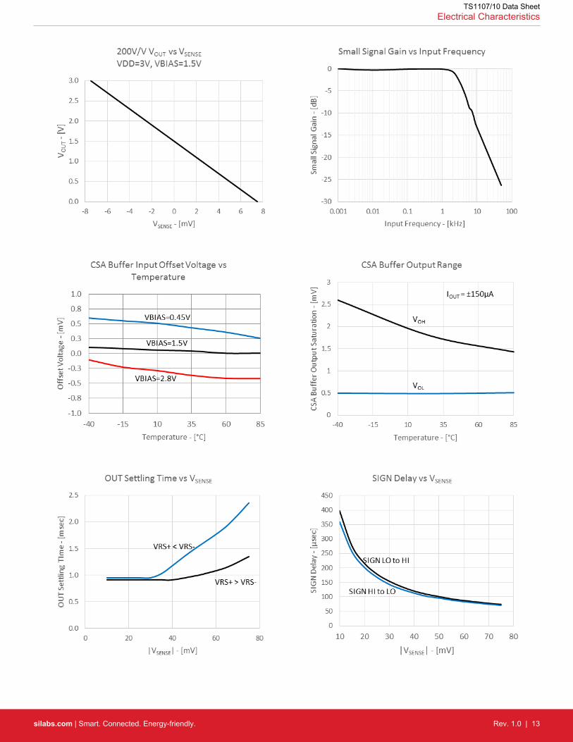
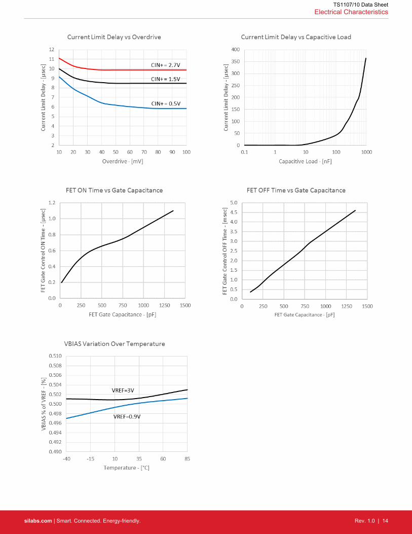
For the following graphs, VRS+ = VRS– = 3.6 V; VDD = 3 V; VREF = GND; VBIAS = 1.5 V, CIN+ = 0.75 V, CLATCH = VDD, CIN– =OUT, RFET = 1 MΩ, CFET = 820 pF, and TA = +25 �C unless otherwise noted.
TS1107/10 Data SheetElectrical Characteristics
silabs.com | Smart. Connected. Energy-friendly. Rev. 1.0 | 11
TS1107/10 Data SheetElectrical Characteristics
silabs.com | Smart. Connected. Energy-friendly. Rev. 1.0 | 12
TS1107/10 Data SheetElectrical Characteristics
silabs.com | Smart. Connected. Energy-friendly. Rev. 1.0 | 13
TS1107/10 Data SheetElectrical Characteristics
silabs.com | Smart. Connected. Energy-friendly. Rev. 1.0 | 14

TS1107/10 Data SheetElectrical Characteristics
silabs.com | Smart. Connected. Energy-friendly. Rev. 1.0 | 15

4. Typical Application Circuit
Figure 4.1. TS1110 Typical Application Circuit
Figure 4.2. TS1107 Typical Application Circuit
TS1107/10 Data SheetTypical Application Circuit
silabs.com | Smart. Connected. Energy-friendly. Rev. 1.0 | 16

5. Pin Descriptions
TS1110 TS1107
Table 5.1. Pin Descriptions
Pin Label Function
1 SIGN Sign output. SIGN is HIGH for VRS+ > VRS– and LOW for VRS– > VRS+.
2 VDD External power supply pin. Connect this to the system’s VDD supply.
3 VBIAS Bias voltage for CSA output. When VREF is activated, leave open.
4 GND Ground. Connect to analog ground.
5 CIN– Inverting terminal of Current Limiter Comparator. Connect to OUT.
6 CIN+ Non-inverting terminal of Current Limiter Comparator. Connect an external reference voltage to set cur-rent limit.
7 NC No connection. Leave open.
8 VREF Voltage reference. To activate, a minimum voltage of 0.9V is required. To disable voltage divider, con-nect to analog ground, GND.
9 OUT CSA buffered output. Connect to CIN–.
10 FILT Inverting terminal of CSA Buffer. Connect a series RC Filter of 4kΩ and 0.47µF, otherwise leave open.
11 RS+ External Sense Resistor Power-Side Connection
12 RS– External Sense Resistor Load-Side Connection. For TS1110 only, connect external PFET’s source toRS– pin and connect load to PFET’s drain. For TS1107, connect load directly to RS– pin.
13 FET TS1110 External PFET Gate Connection. Connect an external pull-down resistor of 1MΩ.
NC TS1107 No connection. Leave open.
14 NC No connection. Leave open.
15 CLATCH Current Limiter Comparator Latch Enable. CLATCH must be HIGH for latch enable. To disable latch,CLACTH must be held LOW.
16 COUT Current Limiter Comparator Output.
Exposed Pad EPAD Exposed backside paddle. For best electrical and thermal performance, solder to analog ground.
TS1107/10 Data SheetPin Descriptions
silabs.com | Smart. Connected. Energy-friendly. Rev. 1.0 | 17

6. Packaging
Figure 6.1. TS1107/10 3x3 mm 16-QFN Package Diagram
Table 6.1. Package Dimensions
Dimension Min Nom Max
A 0.70 0.75 0.80
A1 0.00 0.02 0.05
b 0.20 0.25 0.30
C1 1.50 REF
C2 0.25 REF
D 3.00 BSC
D2 1.90 2.00 2.10
e 0.50 BSC
E 3.00 BSC
E2 1.90 2.00 2.10
L 0.20 0.25 0.30
aaa — — 0.05
bbb — — 0.05
ccc — — 0.05
ddd — — 0.10
Note:1. All dimensions shown are in millimeters (mm) unless otherwise noted.2. Dimensioning and Tolerancing per ANSI Y14.5M-1994.
TS1107/10 Data SheetPackaging
silabs.com | Smart. Connected. Energy-friendly. Rev. 1.0 | 18

7. Top Marking
Figure 7.1. Top Marking
Table 7.1. Top Marking Explanation
Mark Method Laser
Pin 1 Mark: Circle = 0.50 mm Diameter (lower left corner)
Font Size: 0.50 mm (20 mils)
Line 1 Mark Format: Product ID Note: A = 20 gain, B = 200 gain
Line 2 Mark Format: TTTT – Mfg Code Manufacturing code
Line 3 Mark Format: YY = Year; WW = Work Week Year and week of assembly
TS1107/10 Data SheetTop Marking
silabs.com | Smart. Connected. Energy-friendly. Rev. 1.0 | 19

Table of Contents
1. Ordering Information . . . . . . . . . . . . . . . . . . . . . . . . . . . . 1
2. System Overview . . . . . . . . . . . . . . . . . . . . . . . . . . . . . . 22.1 Functional Block Diagrams . . . . . . . . . . . . . . . . . . . . . . . . . 2
2.2 Current Sense Amplifier + Output Buffer . . . . . . . . . . . . . . . . . . . . . 3
2.3 Sign Output . . . . . . . . . . . . . . . . . . . . . . . . . . . . . . 4
2.4 Current Limit Comparator . . . . . . . . . . . . . . . . . . . . . . . . . . 4
2.5 FET Control (TS1110 Only) . . . . . . . . . . . . . . . . . . . . . . . . . 4
2.6 VREF Divider . . . . . . . . . . . . . . . . . . . . . . . . . . . . . . 4
2.7 Selecting a Sense Resistor . . . . . . . . . . . . . . . . . . . . . . . . . 52.7.1 RSENSE Voltage Loss . . . . . . . . . . . . . . . . . . . . . . . . . . 52.7.2 VOUT Swing vs. Desired VSENSE and Applied Supply Voltage at VDD. . . . . . . . . . 52.7.3 Total Load Current Accuracy . . . . . . . . . . . . . . . . . . . . . . . . 52.7.4 Circuit Efficiency and Power Dissipation . . . . . . . . . . . . . . . . . . . . 52.7.5 RSENSE Kelvin Connections . . . . . . . . . . . . . . . . . . . . . . . . 62.7.6 RSENSE Composition . . . . . . . . . . . . . . . . . . . . . . . . . . 62.7.7 Internal Noise Filter . . . . . . . . . . . . . . . . . . . . . . . . . . . 62.7.8 PC Board Layout and Power-Supply Bypassing . . . . . . . . . . . . . . . . . . 6
3. Electrical Characteristics . . . . . . . . . . . . . . . . . . . . . . . . . . . 7
4. Typical Application Circuit . . . . . . . . . . . . . . . . . . . . . . . . . 16
5. Pin Descriptions . . . . . . . . . . . . . . . . . . . . . . . . . . . . . 17
6. Packaging . . . . . . . . . . . . . . . . . . . . . . . . . . . . . . . 18
7. Top Marking. . . . . . . . . . . . . . . . . . . . . . . . . . . . . . . 19
Table of Contents 20

DisclaimerSilicon Laboratories intends to provide customers with the latest, accurate, and in-depth documentation of all peripherals and modules available for system and software implementers using or intending to use the Silicon Laboratories products. Characterization data, available modules and peripherals, memory sizes and memory addresses refer to each specific device, and "Typical" parameters provided can and do vary in different applications. Application examples described herein are for illustrative purposes only. Silicon Laboratories reserves the right to make changes without further notice and limitation to product information, specifications, and descriptions herein, and does not give warranties as to the accuracy or completeness of the included information. Silicon Laboratories shall have no liability for the consequences of use of the information supplied herein. This document does not imply or express copyright licenses granted hereunder to design or fabricate any integrated circuits. The products must not be used within any Life Support System without the specific written consent of Silicon Laboratories. A "Life Support System" is any product or system intended to support or sustain life and/or health, which, if it fails, can be reasonably expected to result in significant personal injury or death. Silicon Laboratories products are generally not intended for military applications. Silicon Laboratories products shall under no circumstances be used in weapons of mass destruction including (but not limited to) nuclear, biological or chemical weapons, or missiles capable of delivering such weapons.
Trademark InformationSilicon Laboratories Inc., Silicon Laboratories, Silicon Labs, SiLabs and the Silicon Labs logo, CMEMS®, EFM, EFM32, EFR, Energy Micro, Energy Micro logo and combinations thereof, "the world’s most energy friendly microcontrollers", Ember®, EZLink®, EZMac®, EZRadio®, EZRadioPRO®, DSPLL®, ISOmodem ®, Precision32®, ProSLIC®, SiPHY®, USBXpress® and others are trademarks or registered trademarks of Silicon Laboratories Inc. ARM, CORTEX, Cortex-M3 and THUMB are trademarks or registered trademarks of ARM Holdings. Keil is a registered trademark of ARM Limited. All other products or brand names mentioned herein are trademarks of their respective holders.
http://www.silabs.com
Silicon Laboratories Inc.400 West Cesar ChavezAustin, TX 78701USA
Smart.Connected.Energy-Friendly
Productswww.silabs.com/products
Qualitywww.silabs.com/quality
Support and Communitycommunity.silabs.com