Embed Size (px)
Citation preview
TRP 5000
INSTRUCTION MANUAL
CONTENTS
Page
1. INTRODUCTION
1 - 1
2. OPERATING INSTRUCTIONS
2.1 Distress Operation on 2182 kHz
2.2 Tuning to 2182 kHz
2.3 Tuning to a Frequency Other than 2182 kHz
2.4 Operating Controls and their Functions
2.5 Filter Cleaning
2 – 1
2 – 1
2 – 1
2 – 2
2 – 2
2 – 2
2 – 5
3. INSTALLATION
3.1 Types of Installations
3.2 Removal of Units
3.3 Mounting the Cabinet
3.4 Connection to the Permanent Installation
3.5 Earth Connections
3.6 Antennas
3.7 Remote Speaker
3.8 Transmitter-on Indication
3.9 Replacement of Power Pack
3.10 Optional Terminal Strips 3.11 Programming of MEMOFIY /238\ , General 3.12 Ordering Programmed PROM’s 3.13 Instruction for use of PROGRAMMING IINIT /241\ 3.14 Adjustment of Antenna Tuning
3 – 1
3 – 1
3 – 1
3 – 1
3 – 1
3 – 2
3 – 3
3 – 5
3 – 5
3 – 5
3 – 5
3 – 7
3 – 8
3 – 14
3 – 17
4. TECHNICAL DATA
4 – 1
5. TECHNICAL DESCRIPTION
5.1 Mechanical
5.2 Circuit Description General
5.3 Circuit Summary, Exciter E 5000
5.4 Circuit Description, Exciter E 5000
5.5 Circuit Summary, Transmitter Power Amplifier T 5000
5.6 Circuit Description, Transmitter Power Amplifier T 5000
5.7 Circuit Summary, 24 V DO Power Pack P 5000
5.8 Circuit Description, 24 V DC Power Pack P 5000
5.9 Circuit Summary, AC Power Pack P5001
5.10 Circuit Description, AC Power Pack P 5001
5 – 1
5 – 1
5 – 1
5 – 2
5 – 3
5 – 10
5 – 10
5 – 11
5 – 12
5 – 14
5 – 14

TRP 5000
INSTRUCTION MANUAL
CONTENTS
Page
6. SIMPLE SERVICE
6.1 Incorrect Operation
6.2 Battery
6.3 Checking the Antenna Tuning
6.4 Using the CHECK SWITCH
6.5 Replacement of Fuses
6 - 1
6 - 1
6 – 1
6 – 1
6 – 1
6 - 2
7. REPAIR AND ALIGNMENT
7.1 Introduction
7.2 Cross Slot Screws
7.3 Locating Sub-units and Components
7.4 Locating Faults
7.5 Test Points
7.6 AC Voltages
7.7 DC Voltages
7.8 Replacement of Valves
7.9 Adjustments
7.10 /232\ Realignment of 1.4 MHz EXCITER
7.11 /233\ Realignment of RF TRANSLATOFT
7.12 /234\ Realignment of CONTROL CIRCUIT AND TONE
GENERATORS
7.13 /235\ Realignment of HARMONIC GENERATOR
7.14 /236\ Realignment of VCO
7.15 /240\ Realignment of MASTER OSCILLATOR
7.16 /251\ Realignment of DRIVER
7.17 /254\ Realignment of VOLTAGE REGULATORS
7 - 1
7 - 1
7 - 1
7 - 1
7 - 1
7 - 1
7 - 1
7 – 2
7 – 2
7 – 3
7 – 4
7 – 5
7 – 8
7 – 9
7 – 10
7 – 10
7 – 10
7 – 10
8. PARTS LISTS AND CIRCUIT DIAGRAMS
8.1 Numbering
8.2 Switches
8.3 Terminals 8.4 Voltages
8.5 Test Points
8.6 Symbol Explanation 8.7 Abbreviations
8.8 Parts Lists
8.8 Block diagram, Exciter E 5000
8 - 1
8 - 1
8 - 1
8 - 1
8 - 1
8 - 2
8 - 2
8 - 5
8 - 60

LIST OF ILLUSTRATIONS
Page Front panel and operating controls
PROM-types which can be installed in the MEMORY /238\
Drilling plan for mounting of TRP 5000
TRP 5000 cabinet, standard version
TRP 5000 cabinet, optional terminal strips installed
Terminal Strip A
Terminal Strip B
Terminal Strip C
Terminal Strip D
Installation of external antenna relay
Initial tab settings, Lower GT band
Initial tab settings, Upper CT band
Initial tab settings, 4-6 MHz bands
Initial tab settings, 8-16 MHz bands
Initial tab settings, 22-25 MHz bands
T 5000 Tuning Chart
Programming Work Sheet
Function table for 234IC5
Function table for 235IC4
Location of circuit boards, E 5000
Location of circuit boards, T 5000
Location of circuit boards, P 5000
Location of circuit boards, P 5001
1-2
3-6
3-20
3-21
3-22
3-23
3-24
3-25
3-26
3-27
3-28
3-29
3-30
3-31
3-32
3-33
3-34
7-11
7-12
8-56
8-57
8-58
8-59

LIST OF DIAGRAMS
Page
Block Diagram, Exciter E 5000
Block Diagram, Transmitter Power Amplifier, T 5000
Block Diagram, 24 V DC Power Pack, P 5000
Block Diagram, AC Power Pack, P 5001
Keying circuit, simplified diagram, 24 V DC
Keying circuit, simplified diagram, AC
/230\ E 5000 Wiring Diagram, /231\ Motherboard
/232\ 1.4 MHz Exciter
/233\ RF Translator
/234\ Control Circuit and Tone Generators
/235\ Harmonic Generator
/236\ VCO
/237\ Frequency Dividers
/238\ Memory
/239\ Display and Keyboard
/240\ Master Oscillator
/241 \Programming Unit
/250\ T 5000 Wiring diagram
/251\ Driver
1252\ Meter Circuit
1253\ Band indicator
/254\ Voltage Regulators
/260\ P 5000 24 V DC Power Pack Wiring Diagram
/261\ Converter-driver, LT-rectifiers and Stabilisers
/262\ HT-rectifiers and Base Keying Circuit
/262\ Driver and Grid Voltage Stabilisers
/264\ input Voltage Sensor
/265\ P 5001 AC Power Pack Wiring Diagram
/266\ LT-stabilisers
/267\ HT-rectifiers
/268\ Driver and Grid Voltage Stabilisers
TRP 5000 Cabinet Wiring
Terminal Strip A
8-60
8-61
8-62
8-63
8-64
8-65
8-67
8-69
8-71
8-73
8-75
8-77
8-79
8-81
8-83
8-85
8-87
8-89
8-91
8-93
8-95
8-97
8-99
8-101
8-103
8-105
8-107
8-109
8-111
8-113
8-115
8-116
8-117

1. Introduction
1.1 The TRP 5000 is a single side band radiotelephone transmitter receiver
combination for duplex, semi-duplex and simplex telephone traffic in
the 1.6-4 MHz coastal telephone band and in the maritime mobile short
wave bands between 4 and 27.5 MHz. In addition the TRP 5000 provides
facilities for radiotelegraph and telex transmission and reception
The TRP 5000 is composed of the T5000transmitter power amplifier, the P
5000 (24 V DC) or the P 5001 (AC) power pack, the E 5000 exciter and
the R 5000 receiver. This instruction manual describes the Transmitter
Power Amplifier, the Exciter and the Power Packs, while the Receiver is
covered in a separate manual.
The transmitter is fully synthesised and provides keyboard selection of
up to 256 pre-programmed frequencies, which can be freely distributed
in the maritime frequency bands.
Silicon transistors and integrated circuits are used throughout except
for the transmitter power amplifier stage. These features in
conjunction with the fact that no crystal ovens are used enable the
transmitter to be ready for operation within 30 seconds after being
switched on.
The cabinet is a sturdy 19-inch rack construction containing all
necessary inter- connections.
Because we are constant processing the experience gained during the
production and operation of our equipment, it is possible for minor
modifications to occur relative to the information given in this
instruction manual. Wherever practicable, however, any corrections will
be listed on a correction sheet at the back of the front cover of this
manual.

1 - 1

1 - 2

2. Operating Instructions
2.1 Distress Operation on,2182 kHz
Set controls as fellows:
A SUPPLY to TRANSMIT
B C BANDs to 2182 kHz
D VOLUME clockwise
E SENSITIVITY fully clockwise
F MODE to TRANSMIT ALARM
G Press and release ALARM START
The alarm signal is now transmitted for approx. 45 seconds and may be
monitored in the handset earpiece. When the alarm signal ceases depress
handset key and, speaking clearly into microphone, transmit distress
message.
If it is required to repeat the alarm signal transmission, it Is only
necessary to press and release the ALARM START push button again.
An alarm signal transmission may be interrupted at any time by turning the
MODE switch to A3H.
NOTE: In the TRANSMIT ALARM mode on 2182 kHz the power output of the
transmitter is automatically set to FULL POWER SIMPLEX independent of
the setting of the POWER switch.
2.2 Tuning to 2182 kHz
1. Set SUPPLY switch to TRANSMIT.
30 seconds after switching on the transmitter is ready for operation.
2. Set BAND switch to 2182 kHz.
The band-indicator lamp will show constant light indicatingthat2182
kHz is selected. The FREQUENCY NO display will extinguish.
3. Press TUNE button and adjust TUNING control for maximum deflection on
ANTENNA CURRENT meter.
The tuning range on 2182 kHz is reduced so that power is transmitted
even when the TUNIN-G control is not adjusted.
The transmitter is now ready for operation.
NOTE: The type of service used on 2182 kHz is A3H, simplex. This mode is
automatically selected when the BAND switch is set to 2182 kHz, and the
MODE switch can therefore be set to any position except TESTALARM. The
equipment will also work in the simplex mode even if the POWER switch is
in a DUPLEX position.

2 - 1

2.3 Tuning to a Frequency Other than 2182 kHz
1. Set SUPPLY switch to TRANSMIT.
30 seconds after switching on the transmitter is ready for operation,
2. Set BAND switch to any band except 2182 kHz
3. Turn DIMMER control fully clockwise
4. If FREQUENCY NO display does not show zero, clear display using C key
of keyboard.
5. Look up desired frequency in frequency chart and read Frequency -No
6. Key Frequency No. into keyboard. The selected Frequency No. will be
displayed.
7. Set BAND switch to position indicated by flashing band indicator lamp.
If no flashing occurs the BAND switch is already correctly set.
8. Press TUNE button and adjust TUNING control for maximum deflection on
ANTENNA CURRENT meter.
9 Select desired type of service with MODE and POWER switches.
Transmitter is now ready for operation
NOTE: Transmission is inhibited if the mode setting does not correspond
with the frequency selected. On radiotelephone frequencies the transmitter
can be keyed only in the modes A3A, A3J, A3H, and TRANSMIT ALARM. On
wireless telegram frequencies the transmitter can be keyed only in the
modes Al, A2H, and Fl.
2.4 Operating Controls and their Functions
2.4.1 The SUPPLY switch has four positions
OFF Receiver and transmitter are switched off.
REGEIVE ONLY Power Pack is started up and supplies power to Receiver
(and grid bias to transmitter output valves). Remote
speaker of receiver is connected to receiver output.
STAND BY Power Pack supplies power to Receiver, Exciter, band
indicator, and filaments of transmitter output valves.
Remote speaker of receiver is connected to receiver
output.
TRANSMIT Transmitter can be keyed. Remote speaker of receiver is
disconnected.
NOTE:A built-in delay circuit protects the output valves of the
transmitter from being keyed for the first 30 sec. after switching to
STAND BY or TRANSMIT.
2 - 2

2.4.2. The POWER switch has six positions
LOW POWER
SIMPLEX
Transmitter is keyed from handset key, morse key, or
telex equipment dependent on mode of operation. Receiver
is muted while transmitting.
Transmitter can be driven to approx. 1/20 Of full output
power.
MEDIUM POWER
SIMPLEX
As above, but transmitter can be driven to approx. 1/4 of
full output power.
FULL POWER
SIMPLEX
As above, but transmitter can be driven to full power.
FULL POWER
DUPLEX
Transmitter is keyed constantly in the Fl, A3A, A3J, A3H
and TRANSMIT ALARM modes (provided the selected frequency
is in accordance with the mode setting). Receiver is on
but built-in speaker is disconnected.
In the A2H and Al modes the operation is simplex
independent of the setting of the POWER switch.
Transmitter can be driven to full output power.
MEDIUM POWER
DUPLEX
As above, but transmitter can be driven to approx. 1/4 of
full output power.
LOW POWER
DUPLEX
As above, but transmitter can be driven to approx. 1/20
of full output power.
NOTE: With the BAND switch set to 2182 kHz, simplex is automatically selected,
independent of the POWER switch setting, and if at the same time the MODE switch
is set to TRANSMITALARM, the transmitter is automatically set to full power.
The MODE switch has eight positions
A2H Transmission of modulated radiotelegraphy. Only the
morse key input is open. The transmitter can only be
keyed if a telegraphy frequency is selected.
Al Transmission of un-modulated radiotelegraphy. Only the
morse key input is open. The transmitter can only be
keyed if a telegraphy frequency is selected.
F1 Transmission of telex. Only the telex inputs are open.
Trans- mission is only possible if a telegraphy
frequency is selected.
TEST ALARM The built-in two tone alarm generator is connected to
the receiver AF amplifier. Transmitter cannot be keyed.
A3A Transmission of single-side band signal with reduced
carrier. Transmission is only possible if a radio
telephony frequency is selected. The transmitter can be
keyed from the hand set key or by setting the POWER
switch to DUPLEX.
A3J As above, but carrier suppressed
A3H As above, but full carrier.
TRANSMIT ALARM The two-tone alarm generator is connected to the
receiver AF amplifier and the alarm generator is ready
for transmission of an alarm signal. The mode is A3H as
above.

2 - 3

2.4.4 The ALARM START push-button is used to start the alarm generator after
the MODE switch has been turned to the TRANSMIT ALARM position. The
push-button is depressed and released and the alarm signal will be
transmitted for approx. 45 seconds.
The push-button is also used for starting the alarm generator in the
TEST ALARM position.
2.4.5 The KEYBOARD is used for frequency selection. It controls the frequency
memory. The programmed frequencies are listed in the frequency chart.
Each frequency is supplied with a number and this number is keyed into
the keyboard. The frequency number selected is displayed on the
FREQUENCY NO display.
The display is cleared by using the C-key, which resets the display to
zero.
The display extinguishes when the BAND switch is set to 2182 kHz, but
keyboard entry is still possible and the display will show the selected
Frequency No. when the BAND switch is turned away from 2182 kHz.
If an un-programmed Frequency No is selected, the display will start to
flash, indicating that transmission is not possible.
2.4.6 The DIMMER controls the intensity of the FREQUENCY NO display.
2.4.7 The TUNING control is used for tuning the antenna circuit to maximum
antenna current indicated on the ANTENNA CURRENT meter.
2.4.8 The BAND switch has 16 positions:
2182 kHz The FREQUENCY NO display is extinguished and the band-
indicator lamp shows constant light indicating that 2182 kHz is
selected. The range of the TUNING control is reduced. The A3H,
simplex mode is automatically selected.
Bands A to H cover the coastal telephone band 1.6 to 4 MHz.
The 4 MHz, 6 MHz, 8 MHz, 12 MHz, 16 MHz, 22 MHz, and 25 MHz positions
cover the maritime short-wave bands.
A band indicator lamp at each position shows by flashing light where to
set the BAND switch in accordance with the Frequency No selected. The
light will extinguish when the BAND switch is set at the correct
position.
2.4.9 The TUNE push-button is used when tuning the antenna circuit. The
transmitter is keyed and a tune signal is generated. During tuning, the
receiver is muted.

2 – 4

2.4.10 The CHECK SWITCH is not normally operative. Pulling the switch knob out
will switch the ANTENNA CURRENT meter to read the voltage or current
selected with the switch. When released, the knob will return to its
original position.
The switch has eight positions:
LEVEL Check of anode AG voltage swing
VA Check of anode DC voltage
Vs1 Check of screen grid voltage of valve no. 1
Vs2 Check of screen grid voltage of valve no. 2
VG Check of grid bias
I1 Check of cathode current of valve no. 1
I2 Check of cathode current of valve no. 2
VD Check of supply voltage to driver amplifier.
2.5 Filter Cleaning
The air filter on the transmitter power amplifier front panel should be
cleaned periodically. The filter element is easily removed without the
use of tools. Wash in warm water and dry thoroughly.

2 - 5

Installation
Correct installation of the equipment is important for maximum performance
and reliability. Antennas and earth connections must be installed with the
greatest care, especially where duplex telephony is desired.
3.1 Types of Installation
The TRP 5000 radiotelephone may be powered from either a
24V battery or from 110/115/120/220/230/240V-AC mains.
The TRP 5000 is composed of the following units:
For 24V battery operation:
Type T 5000 transmitter power amplifier
Type P 5000 power pack
Type E 5000 / E5001 exciter
Type R 5000 / R5001 receiver
For AC mains operation (single-phase or two-phase):
Type T 5000 transmitter power amplifier
Type P 5001 power pack
Type E 5000 / E5001 exciter
Type R 5000 / R5001 receiver
The units are connected together in the TRP5000 cabinet in which also the
connections to the permanent installation are made.
3.2 Removal of units
After removal of the front-panel screws, the units may be pulled out as
far as the built-in stops permit. The cables may be unplugged and the
individual units removed entirely from the cabinet after having released
the stop latches. This is done by pushing the unit slightly back into the
cabinet (approx. 10 mm) and pressing the two nylon knobs of the latches at
the sides of the unit while pulling the unit out.
For ease of removal of the units start with the lowest and proceed
upwards. The reverse order is used when refitting the units.
3.3 Mounting the Cabinet
The cabinet is supplied with shock absorbers. The drawing on page3-
20showsthe drilling plan for the necessary holes.
3.4 Connection to the Permanent Installation
Check that the correct power pack is installed in the equipment and, in
case of AC operation, set f or the correct mains voltage. The drawing of
Terminal strip A on page 3-23 shows the marking of the terminals to be
used for the installation. Necessary cable cross sections are also
indicated. All cables except the transmitter antenna and earth leads are
brought through the cut out in the cabinet rear wall in a loop that is
large enough to take up any play between the equipment and the bulkhead.
3 – 1

A mains switch and fuses are to be provided in the supply leads. External
fuse ratings are listed in Table 3.1.
Power Pack Supply Voltage External Fuses
P 5000
24V
DC
5OA
P 5001
110V
115V
120V
50-60
Hz
20A
P 5001
220V
230V
240V
50-60
Hz
15A
Table 3.1
3.4.1 Supply Voltage Changing in P 5001 (AC operation) :
Voltage Changing in the P 5001 power pack is carried out by unsoldering
the connections to and between the terminals of the two transformers
265 TI and 265 T2.
The necessary connections are shown on the diagram of P 5001.
When changing voltage it is also necessary to replace the fuse in the
power pack input lead. Fuse rating is given on the P 5001 diagram.
3.5 Earth Connections
As the transmitter earth connection is always a part of the total
antenna system, it is of the utmost importance that the earth
connection is constructed to have the smallest possible RF-impedance.
Losses in the earth connection will result in a decrease in radiated
power which means that the range of the transmitter will be reduced. A
poor earth connection will further impede or even make duplex
communication impossible.
3.5.1 Transmitter Earth Terminal:
The transmitter earth terminal is located on the top of the cabinet.
3.5.1.1 Steel Ships:
From the transmitter earth terminal a 100x0.5 mm copper strap is run
un-interrupted to two 1/2" bolts welded to the hull as close to the
equipment as possible

3 – 2

3.5.1.2 Wooden Ships:
From the transmitter earth terminal a 100x0.5 mm copper strap is run,
preferably uninterrupted, to an earth bolt welded to an earth plate
having a minimum area of 1 m2 mounted under the water line. Should it,
however, be necessary to break the copper strap, for example to pass
through a deck, two 1/2" bolts should be used for this feed through.
The copper strap should then be continued below deck, after connection
to the same two bolts.
The copper strap must not be passed through iron pipes and should be
kept a minimum distance of 0.5 m from iron parts of some extent. If
this minimum distance cannot be kept the copper strap must be
effectively connected to these parts using a strap having the same
dimensions.
On wooden ships having a superstructure of metal, this superstructure
should also be effectively connected to the copper strap.
5.2.2 Receiver Earth Terminal
The receiver earth terminal is located on terminal strip A at the
cabinet rear wall
3.5.2.1 Steel Ships
A flexible 2.5 MM2earth wire is run from the receiver earth terminal to
a separate/2" earth bolt welded to the hull as close to the equipment
as possible. This earth bolt must not be used for earthing other
equipment, and the receiver earth wire shall be as far as possible from
the transmitter copper strap.
3.5.2.2 Wooden Ships
A flexible 2.5 MM2 earth wire is run from the receiver earth terminal
directly to the transmitter earth bolt on the earth plate. The earth
wire should be run a minimum distance of 0.5 m from the transmitter
copper strap.
3.5.3 Other Cables
Other cables should be placed as far away as possible from the
transmitter and receiver earth leads and under no circumstances
parallel with the transmitter copper strap closer than 0.7 meter and,
for the receiver earth lead, closer than 0.2 meter.
3.5.4 Earthing the Battery
RF earth connections will cause neither battery nor mains leads to be
connected to the hull. If it is desired to connect the battery to the
hull, it is important to make the connection right at the battery,
never in the transmitter. In cases where the installation is carried
out so as to include the facility for charging during operation through
a dropping resistor from a balanced ship's mains (110/220V DC), the
battery must not be earthed.
3.6 Antennas
In order to minimise duplex noise, the transmitting and receiving
antennas should be kept as far away from each other as possible. Stays,
wires, steel masts etc. should either be earthed effectively or
insulated.

3 – 3

Like wise in order to minimise duplex noise, every other electric
installation such as cable braiding (screens) and instruments should be
earthed effectively, and the instruments in question should be fitted
with noise-interference suppression devices.
The Antennas should be suspended well in the clear, away from objects
whose influence on the antennas may vary, such as derricks etc.
Insulators should be of the best type having low leakage even when wet.
3.6.1 Transmitter Antenna Terminal:
The transmitter antenna terminal is located on the top of the cabinet.
3.6.2 Transmitter Antenna
The transmitter antenna tuning system will tune a minimum impedance of
150 p Fin series with 6 ohms at 1.6 MHz which normally corresponds to a
wire length of approx.14 m.
To ensure the greatest possible radiated power the transmitter antenna
should be as long as possible and although a length of 14 meter can be
tuned it is strongly recommended never to use lengths less than 20 m as
the radiated power from short antennas will result in unsatisfactory
communication. There are no limitations
regardingthemaximumlengthoftheantranna.Theantennashouldbeterminatedin a
feed-through insulator in the roof or side wall of the radio room. The
feed-through insulator should be located in such a way that the
distance between the insulator and the transmitter antenna terminal is
as short as possible to avoid losses and radiated RF-power inside the
radio-room which might disturb other equipment.
A short length of coaxial cable type RG8-U, of which only the braid and
the outer insulation is used, is inserted between the feed-through
insulator and the transmitter antenna terminal. Both ends of the
coaxial screen are soldered to cable shoes of suitable dimensions for
the feed-through insulator and the transmitter antenna terminal.
lf, for practical reasons, it should be necessary to mount the feed-
through insulator some distance f rom the transmitter, the connection f
rom the insulatorto the vicinity of the transmitter should be done with
a -length of copper tubing mounted on stand-off insulators. A length of
coaxial cabie, as described above, should then be inserted between the
last stand-off and the transmitter antenna terminal; any play between
the transmitter and buikhead will then be taken up by the cable.
3.6.3 Receiver Antenna Terminal:
The receiver antenna terminal is located on term in al strip A at the
cabinet rear wall.
3.6.4 Receiver Antenna:
Length: 7-50 m. The receiving antenna should be brought in by a length
of coaxial cable, which should be as short as possible, especially in
the case of a short antenna.
3 – 4

If a long coaxial cable is used in order to separate receiver and
transmitter antennas it wilt often be advantageous to insert an
impedance matching transformer at the antenna end of the coaxial cable.
While the receiver input impedance is always 50 ohm at frequencies
above 4 MHz, the receiver is normally supplied with a high impedance
input at frequencies below 4 MHz. It is however possible to change the
receiver input impedance to 50 ohms also at frequencies below 4 MHz.
Reference is made to the receiver instruction manual.
Antenna Relay:
As shown on the drawing on page 3-27, an antenna relay may be installed
in the antenna circuit. The relay may be installed if the transmitting
antenna is to be used for other purposes, for instance for an extra
receiver, or if it is desired to perform the installation as a simplex
installation with only one antenna. The relay coil should be rated for
24V DC. It should be connected to terminals 3 (+) and 4 (-) on terminal
strip A and protected with a suitable diode.
3.7 Remote Speaker
If a remote speaker is to be installed it should be connected to
terminals 1 and 2 of terminal strip A
Note that the remote speaker will be connected to the receiver only
when the SUPPLY switch is at RECEIVE ONLY and STAND-BY.
An audio power of 5 watts is available into a 4 ohms load. This power
can be shared between several loudspeakers if so desired. The built-in
speaker in the power pack has an impedance of 8 ohms. When connecting
the remote speaker(s) the minimum value of the total impedance should
be 4 ohms including the built-in speaker. If 5 watts is required in the
remote speaker(s), the built-in speaker must be switched off.
3.8 Transmitter-On Indication
Indication of the transmitter-on condition can be obtained by means of
a voltage (24V at max. 0.2A) which is controlled by the transmit relay
and can be taken off between terminals 3 (+) and 4 (-) of terminal
strip A.
3.9 Replacement of Power Pack
Two different power packs are available for operation of the equipment.
The P 5000 is used for24V battery operation. If the equipment is to be
operated from AC-mains the P5001 power pack must be used. Replacing a
power pack involves no modifications of transmitter or receiver.
3.10 Optional Terminal Strips
Three optional terminal strips are available. The terminal strips are
supplied with cables .and plugs and are to be mounted on the cabinet
back wall as shown on page 3-22.
Output Terminal Strip B gives a number of extra output facilities as
shown on page 3-24 and is to be connected to the Power Pack.
3-5

Input Terminal strip C, shown on page 3-25, is to be connected to the
Exciter.
Output Terminal Strip D, shown on page 3-26, is intended to be
connected to the Transmitter Power Amplifier and can be used for
example where it is desired to control an ATU. The corresponding socket
in the T5000 is only mounted and wired on special order, but a BAND
switch wafer which can be wired to give the BAND position is always
supplied as an integral part of the Transmitter Power Amplifier.
PROM-types which can be installed in the MEMORY of /238\
Manufacturer Types
INTERSIL
INTERSIL
IM 5600
IM 5610
TI
TI
TI
TI
TI
TI
SN 54188
SN 54188 A
SN 54S188
SN 74188
SN 74188 A
SN 74188
Only these PROM-
types can be
programmed by means
of the optional
PROGRAMMING UNIT
/241\
Table 3.11

3 - 6

3.11 Programming of MEMORY /238\, General
3.11.1 The building block of the memory, located on printed circuit board /238\
, is the Programmable Read Only Memory, in short PROM.
A PROM is not re-programmable, because programming a bit position is
like blowing a fuse.
3.11.2 On printed circuit board /238\ 24 PROM’s can be mounted in separate
sockets. The24soeketsareformed into eight columns (No. 1 to No.8), each
containing three sockets (A, B, and C). The necessary information
associated to a Frequency No is stored in three PROM’s in a column. Each
column can contain information of 32 different Frequency Nos. The
association between the Frequency No’s and the column No’s is shown in
table 3.12.9.
3.11.3 The programming of the PROM’s can done in two ways.
The optional PROGRAMMING UNIT /241\ can be used for this job as
described in paragraph 3.13. But only the eight peace’s shown in the
table 3.11.1 can be programmed by means of printed circuit board /241\
The other way is to let the local PROM-distributor do the programming.
In this case all the PROM-type shown in table 3.1 1.1 can be used in the
MEMORY /238\.
3.11.4 The MEMORY /238\ controls the Band Indicator of Transmitter Power
Amplifier. This implies that the distribution of the coastal telephone
frequencies in the bands A to H have to be decided in advance when
programming the memory.
Each position of the Transmitter Power Amplifier BAND switch can, in
principle, be adjusted to any frequency, but once adjusted (during
installation on board a ship) the frequency coverage of each band is
limited. In order to obtain a reasonable output power, the difference
between the highest and the lowest frequency within a band should not
exceed approx. 200 kHz.
Table 3.11.2 suggests a subdivision of the coastal telephone band based on
article 7, section 4 (1976) of the Radio Regulations. If, however,
special frequencies are to be covered, another subdivision may be
necessary. Further, table 3.11.2 shows the frequency ranges of the HF
bands covered by the Exciter.
Transmitting
frequency (kHz)
BAND Transmitting
frequency (kHz)
BAND
1605-1670
1950-2150
2150-2350
2350-2550
2550-2750
3000-3200
3200-3400
3400-3600
A
B
C
D
E
F
G
H
4063 - 4219.4
6200 - 6325.4
8195 - 8435.4
12330 - 12652.3
16460 - 16859.4
22000 - 22310.5
25010 - 25600
4 MHz
6 MHz
8 MHz
12 MHz
16 MHz
22 MHz
25 MHz
Table 3.11.2

3 - 7

3.11.5 Information about the transmitting mode of every Frequency No. in use
must be stored in the memory, whether it is a radiotelephone frequency
(A3A,A3J, orA3H)or a wireless telegraph frequency (Al, A2H, or Fl).
3.11.6 Programming Frequency No. zero can be done in two ways.
If it is convenient that this Frequency No. contains the information
associated with an often used transmitting frequency, the programming
instructions do not differ from the instructions concerning any other
Frequency No.
On the other hand, if it is not desired to store any transmitting
frequency information associated with Frequency No. zero, this can
either be done as described in paragraph 3.12.14, if it is convenient
to let the local PROM-distributor do the programming, or in paragraph
3.13.22 If the programming is performed by means of the optional
PROGRAMMING UNIT /241\
3.11.7 The easiest method of checking the programmed frequencies when the
PROM's have been mounted in the MEMORY /238\ is by connecting a
frequency counter to the output BNC socket, 231SK7, of the Exciter. The
output socket is the one carrying no colour code. It is normal
connected to the Transmitter Power Amplifier via a coaxial cable.
Unplug the cable and connect the counter to this socket.
The check is made with the SUPPLY switch in STAND BY. The frequency
measured is the transmitting frequency, ft. Radiotelephone frequencies
are measured in the A3H mode, DUPLEX. Wireless telegraph frequencies
are measured in the Al mode, morse key down.
3.12 Ordering programmed PROM’s
3.12.1 To make it possible for the local PROM-distributor to do the
programming the customer must fill in a Word Pattern Sheet, supplied by
the distributor, for each PROM which is to be programmed.
3.12.2 First of all one must find out which of the 32 input addresses of the
PROM corresponds to the wanted Frequency No. It is done in accordance
with table 3.12.1.
Frequency No.
(both
included)
Input Address
equal to:
0- 31
32- 63
64- 95
96-127
128-159
160-191
192-223
224-255
(Frequency No.)
(Frequency No.) – 32
(Frequency No.) - 64
(Frequency No.) – 96
(Frequency No.) –128
(Frequency No.) –160
(Frequency No.) –192
(Frequency No.) -224
Table 3.12.1
3 - 8

3.12.3 Now the proper BAND corresponding to the transmitting frequency is to be
found. If it is a coastal telephone frequency paragraph 3.11.4 describes
what to do-
The encoding of the different BAND’s is shown in table 3.12.2.
BAND Code
A
B
c
D
E
F
G
H
4 MHz
6 MHz
8 MHz
12 MHz
16 MHz
22 MHz
25 MHz
MF
0000
0001
0010
0011
0100
0101
0110
0111
1000
1001
1010
1011
1100
1101
1110
1111
Table 3.12.2
3.12.4 The transmitting mode is encoded as follows
MODE CODE
A3H, A3A, or A3J
Al, A2H, or Fl
0
1
Table 3.12.3
3.12.5. Calculate the synthesiser frequency fs from the transmitting frequency
ft as shown in tabie3.12.4. Observe that the transmitting frequency ft
is the carrier frequency in the modes A2H, Al, A3A, A3J and A3H. In the
Fl-mode ft is the assigned frequency, provided that the centre
frequency of the AF output from the telex equipment is 1500 Hz. If the
AF centre frequency is 1700 Hz, subtract 200Hz from the assigned
frequency to obtain ft.
BAND
Fs
Synthesiser
frequency
1605-4000 KHz
4 MHz
6 MHz
8 MHz
12 MHz
16 MHz
22 MHz
25 MHz
ft + 1400 KHz
ft + 1400 KHz
ft - 2800 KHz
ft - 4200 KHz
ft - 8400 KHz
ft - 12600 KHz
ft - 18200 KHz
ft - 21000 KHz
Table 3.12.4

3 - 9

3.12.6 Each of the four least significant digits of the synthesiser frequency
("100 kHz", "10 kHz", "l kHz", and "100 Hz") are encoded as follows:
Number Code
0
1
2
3
4
5
6
7
8
9
1001
1000
0111
0110
0101
0100
0011
0010
0001
0000
Table 3.12.5
3.12.7 The most significant digit of the synthesiser frequency ("l MHz")
is encoded as follows.
Number Code
3
4
5
10
01
00
Table 3.12.6
3.12.8 In order to store this information 3 PROM’s must be programmed at the
same input address. These 3 PROM’s are labelled A, B, and C. The total
amount of information should now be arranged as follows:
Input
Address
Control
bit
Band Mode Synthesiser frequency
1MHz 100KHz 10KHz 1KHz 100Hz
1 07 06050403 02 0100 07060504 03020100 07060504 03020100
PROM-C PROM-B PROM-A
(00 to 07 indicates outputs to be programmed).
Table 3.12.7
3.12.9 NB. The code of the "Control bit- is always to be 1 for each Frequency
No. to be programmed.

3 - 10

3.12.10 Example 1:
Assume that the telex frequency 4170.0KHz is to be programmed at
Frequency No. 83.
The input address can be found from table 3.12.1:
Input address = 83-64 = 19
(1)
According to paragraph 3.12.9 the Control bit is set to 1
(2)
According to table 3.12.2:
BAND = 4 MHz Code = 1000
(3)
The code for the Fl mode is, according to table 3.12.3 :
1
(4)
The synthesiser frequency can be calculated from table 3.12.4
fs = 4170.0KHz + 1400.0KHz = 5570.0KHz
By use of table 3.12.5 and table 3.12.6 the associated codes can be
found :
Digit Number Code
1 MHz
100 KHz
10 KHz
1 KHz
100 Hz
5
5
7
0
0
00
0100
0010
1001
1001
(5)
(6)
(7)
(8)
(9)
The total amount of information is now to be arranged :
(1) (2) (3) (4) (5) (6) (7) (8) (9)
Input
Address
Control
bit
Band Mode Synthesiser frequency
1MHz 100KHz 10KHz 1KHz 100Hz
19 1 1000 1 00 0100 0100 1001 1001
1 07 06050403 02 0100 07060504 03020100 07060504 03020100
PROM-C PROM-B PROM-A
Table 3.12.8a

3 – 11

Example 2:
Assume that a radio telephone frequency 3550.0KHz is to be programmed at
Frequency No. 228.
The input address can be found from table 3.12.1:
Input address = 228-224 = 4
(1)
According to paragraph 3.12.9 the Control bit is set
to 1
(2)
According to table 3.11.2 and table 3.12.2:
BAND = H, Code = 0111
(3)
The code for the radio telephony mode is, according
to table 3.12.3: 0
(4)
The synthesiser frequency can be calculated from tabie 3.12.4:
fs = 3550.0KHz + 1400.0KHz = 4950.0KHz
By use of table 3.12.5 and table 3.12.6 the associated codes can be
found:
Digit Number Code
1 MHz
100 KHz
10 KHz
1 KHz
100 Hz
4
9
5
0
0
01
0000
0010
1001
1001
(5)
(6)
(7)
(8)
(9)
The total amount of information is now to be arranged:
(1) (2) (3) (4) (5) (6) (7) (8) (9)
Input
Address
Control
bit
Band Mode Synthesiser frequency
1MHz 100KHz 10KHz 1KHz 100Hz
4 1 0111 0 01 0000 0100 1001 1001
1 07 06050403 02 0100 07060504 03020100 07060504 03020100
PROM-C PROM-B PROM-A
Table 3.12.8b
3 – 12
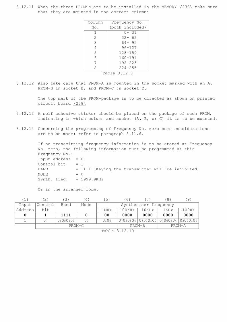
3.12.11 When the three PROM’s are to be installed in the MEMORY /238\ make sure
that they are mounted in the correct column:
Column
No.
Frequency No.
(both included)
1
2
3
4
5
6
7
8
0- 31
32- 63
64- 95
96-127
128-159
160-191
192-223
224-255
Table 3.12.9
3.12.12 Also take care that PROM-A is mounted in the socket marked with an A,
PROM-B in socket B, and PROM-C ;n socket C.
The top mark of the PROM-package is to be directed as shown on printed
circuit board /238\
3.12.13 A self adhesive sticker should be placed on the package of each PROM,
indicating in which column and socket (A, B, or C) it is to be mounted.
3.12.14 Concerning the programming of Frequency No. zero some considerations
are to be made; refer to paragraph 3.11.6.
If no transmitting frequency information is to be stored at Frequency
No. zero, the following information must be programmed at this
Frequency No.:
Input address = 0
Control bit = 1
BAND = 1111 (Keying the transmitter will be inhibited)
MODE = 0
Synth. freq. = 5999.9KHz
Or in the arranged form:
(1) (2) (3) (4) (5) (6) (7) (8) (9)
Input
Address
Control
bit
Band Mode Synthesiser frequency
1MHz 100KHz 10KHz 1KHz 100Hz
0 1 1111 0 00 0000 0000 0000 0000
1 07 06050403 02 0100 07060504 03020100 07060504 03020100
PROM-C PROM-B PROM-A
Table 3.12.10

3 - 13

3.13 Instruction for use of PROGRAMMING UNIT /241\
3.13.1 Three sockets are located in the PROGRAMMINGUNIT. From MEMORY /238\ the
three PROM’s in the column No. found from table 3.12.9 are moved to
board /241\ and mounted in these three sockets.
Take care that the one placed in socket A on /238\ is mounted in the
socket marked with an A, socket B in socket B, and socket C in socket
C. Also take care that the top mark of the PROM package is directed as
shown on /241\.
3.13.2 A minor dis-advantage associated with the use of the PROM as the memory
building block is that a few per cent of the PROM’s cannot be
programmed in one or more bit positions due to tolerance problems in
the manufacturing process. In this case section 3.13.17 describes what
to do.
3.13.3 Because PROM is not re-programmable the greatest care should be taken
concerning the programming procedure.
3.13.4 For each Frequency No. the following information must be stored in the
PROMS. This information should be written on a Programming Work Sheet
as shown on page 3-34.
3.13.5 The proper BAND corresponding to the transmitting frequency is to be
found from table 3.11.2 if it is a coastal telephone frequency,
otherwise it is self explanatory.
3.13.6 It must be decided whether it is to be a radiotelephone
frequency(RT=A3H,A3A,or A3J) or a wireless telegraph frequency (WT =
Al, A2H, or Fl).
3.13.7 Furthermore the synthesiser frequency must be calculated from the
transmitting frequency as shown on the screening lid to the right of
the PROGRAMMING UNIT or in table 3.12.4.
3.13.8 By means of the ON-OFF switch on /241\ this unit is turned on.
3.13.9 A the sliders of the programming tool are now adjusted according tot
his information. In the other window some holes will appear and these
are the positions which must be programmed.
3.13.10 By means of the Keyboard on the front panel the Frequency No., which is
to be programmed, is selected. (The displays may flash during the
programming procedure, but this is unimportant).
3.13.11 If the lamp of the grey pushbutton is now lit, it means that the
Frequency No. chosen has already been programmed once, and further
programming is automatically inhibited.
3.13.12 On the other hand if the above mentioned lamp is unlit, it means that
programming can now be done.
3.13.13 The Programming Pin is now placed in the extreme right hole in the
window. The lamp of the red pushbutton will light as long as the
Programming Pin does not have proper contact with the Underlying
socket-terminal or if this hole position has already been programmed.

3 – 14

3.13.14 Now activate the red pushbutton.
3.13.15 If the programming was done successfully the lamp of the red push
button will now light and the Pin is moved to the next hole.
3.13.16 If the programming was not done successfully, the red push button must
be activated repeatedly until the lamp is lit.
3.13.17 If it turns out that it is impossible to program this hole position,
the only thing to do is to choose another Frequency No. and start to
program all over again. Later on, when the PROM’s are installed on
/238\ , the transmitter is automatically prevented from being keyed, if
this unsuccessfully programmed Frequency No. is chosen; this will also
be indicated by the displays, which will begin to flash.
3.13.18 If all the hole positions in the window have been successfully
programmed, the Programming Pin must be placed in the hole in the
middle of the tool, and this position is then to be programmed.
3.13.19 This will make the lamp of the grey pushbutton light, thus indicating
that this Frequency No. is correctly programmed; any attempt to program
further information at this Frequency No. is now automatically
prevented.
3.13.20 If, later on, it turns out that nevertheless a mistake was made, when
the sliders were adjusted, and the »Enable» hole position had been
programmed, it is still possible to »Disable» the Frequency No. This is
done as follows.
3.13.21 Adjust the "MHz"-slider so that a black field appears in the window;
two holes will now appear in the other window; now push and keep down
the grey pushbutton until both of these two hole positions are
programmed, as normal by means of the Programming Pin and the red
pushbutton. When this has been accomplished, it will prevent the
transmitter from being keyed when the PROM’s are mounted on /238\. If
this Frequency No. is chosen; this will also be indicated by means of
the flashing displays.
3.13.22 Concerning the programming of Frequency No. Zero some considerations
are to be made, refer to paragraph 3.11.6.
3.13.23 If no transmitting frequency information is to be stored at Frequency
No. zero, the following procedure must be followed.
Adjust the Band-slider so that an "MF" appears in the window; only the
associated four hole positions and after wards the Enable position in
the middle of the tool must be programmed.
This will, when the three PROM’s are mounted on /238\, prevent the
displays and the Band Indicator from flashing and also prevent the
transmitter from being keyed when Frequency No. zero is chosen.
3.13.24 When the programming of the Frequency No’s has been accomplished the
PRO- GRAMMING UNIT is turned off, the Programming Pin is placed in its
holding clips, and the three PROM’s are moved back to the MEMORY /238\.
Take care that the PROM’s are mounted in the correct way and in the
correct sockets.

3 - 15

3.13.25 A self adhesive sticker should be placed on the package of each PROM
indicating in which column and socket (A, B, or C) it is to be mounted.
3.13.26 Programming procedure step by step
l. Calculate for each Frequency No. the synthesiser frequency from the
transmitting frequency as shown in table 13.12.4, find the correct BAND
(for a coastal telephone frequency table 3.11.2 is used), and decide
whether it is to be a radiotelephone frequency (RT) or a radiotelegraph
frequency (WT)
2. Mount the three PROMS in their respective sockets on /241\. (Take care
that they are correctly positioned).
3. Turn on the PROGRAMMING UNIT
4. Adjust the seven sliders according to step 1
5. Select by means of the Keyboard the Frequency No. to be programmed (The
displays may now flash, but this is unimportant).
If the lamp of the grey pushbutton lights, the Frequency No. chosen has
already been programmed and a new Frequency No. must be selected.
6. Place the Programming Pin in one of the holes in the window of the
tool; beginning from the right.
If this hole position is un-programmed the lamp of the red pushbutton
will extinguish.
7. Activate the red pushbutton
The lamp of the red pushbutton will now light if the programming was
successful.
As long as there are un-programmed hole positions the steps 6 and 7 are
repeated.
If the lamp of the red pushbutton does not light, step 7 is repeated
until it lights. (]f this turns out to be impossible then proceed to
step g).
8. Program "Enable" hole position in the middle of the Programming Tool,
thus enabling this Frequency No.
If there are more Frequency No’s to program then go back to step 4,
otherwise to step 16.
If there is a hole position, which cannot be programmed
9. Select a new un-programmed Frequency No. and start from step 6
If it turns out, after having performed step 8, that a mistake was made
concerning the information already programmed:
10. Adjust the "MHz"-slider, so that a black field appears in the window
11. Place the Programming Pin in one of the two associated holes
3 - 16

12. Push and keep down during step 13 the grey pushbutton.
13. Activate the red pushbutton.
14. Move the Programming Pin to the other hole and repeat the steps 12 and
13.
15. Go back to step 4 and repeat through to step 8
16. Turn off the Programming Unit.
17. Place the Programming Pin in its holding clips.
18. Place a self adhesive sticker on the package of each PROM, indicating
in which column and socket (A, B, or C) it is to be mounted on MEMORY
/238\.
19. Move the three PROM’s to /238\. (Take care that they are mounted in the
correct way and in the correct sockets).
3.14.1 The drum switch of the antenna tuning circuit becomes accessible by
pulling the Transmitter Power Amplifier unit partly out of the cabinet.
As connections to earth and antenna are maintained, it is possible to
perform the adjustments with the Transmitter Power Amplifier in this
position. When adjustment has been completed it ought to be checked
with the unit in place. Minor corrections may be necessary.
The safety switch, that normal prevents keying when the transmitter
power amplifier unit is pulled out, has to be disabled. The piston of
the switch has to be pulled outwards to the locked position.
Note: Extreme care has to be taken as high tension is now accessible when the
SUPPLY switch is in position TRANSMIT.
The various components of the antenna tuning circuit are selected by
means of the drum switch which can be programmed individually for each
band by inserting programming tabs into the appropriate wafers. The
distribution of frequencies into the bands has been determined when
programming the MEMORY /238\ as described in section 13.11.
It is important that the adjustments are made with the antenna in its
normal working positioned that no cranes, derriks, etc. are near, as
these will influence the tuning.
The meter on the front panel indicates the actual antenna current.
Since the antenna impedance varies considerably over the frequency
range, the antenna current will vary correspondingly, even though the
output power is the same. If the antenna length is approximately half a
wavelength or a multiple thereof, the meter reading will be very low.
If this is un-desirable, a higher reading can only be obtained by
shortening or lengthening the antenna.
Due to the wide adjustment range when programming the drum switch,
attention must be drawn to the possibility of erroneously adjusting to
the second harmonic frequency. The only sure method of checking this is
by means of a frequency counter or an oscilloscope connected to a loop
around the antenna insulator of the transmitter. Check one frequency in
each band. (A3H or A3A DUPLEX, TUNE button not pressed).
3 - 17

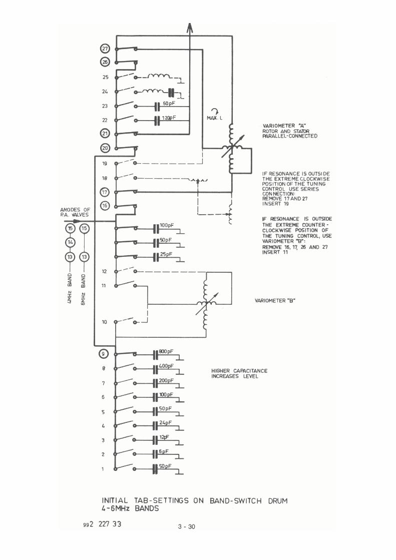
3.14.2 Band’s A to H
The configuration is basically an L-network, the series inductance of
which consist of may consist of variometer -A-.The rotor and stator of
variometer can be used on the lower frequencies, giving a high value of
inductance. The parallel connection is to be used on the higher
frequencies, giving a lower value of inductance. The transition
frequency depends on the antenna.
The shunt capacitance, in parallel to the P.A. valves, can be selected
between 6 and 1600pF in steps of 6 pF by means of 1 to 9. Increasing
the shunt capacitance while still having resonance (by adjusting the
variometer by means of the tuning knob) decreases the voltage swing on
the P.A. valves ( the load presented to the valves becomes lower) and
vice versa.
If the antenna is long, it may be necessary to use the shortening
capacitors or the output capacitor (wafers 22, 23, and 24 or any
combination of these) in order to obtain resonance. If the antenna is
short, it may be necessary to use the output capacitor (wafer 24) on
the lowest frequencies.
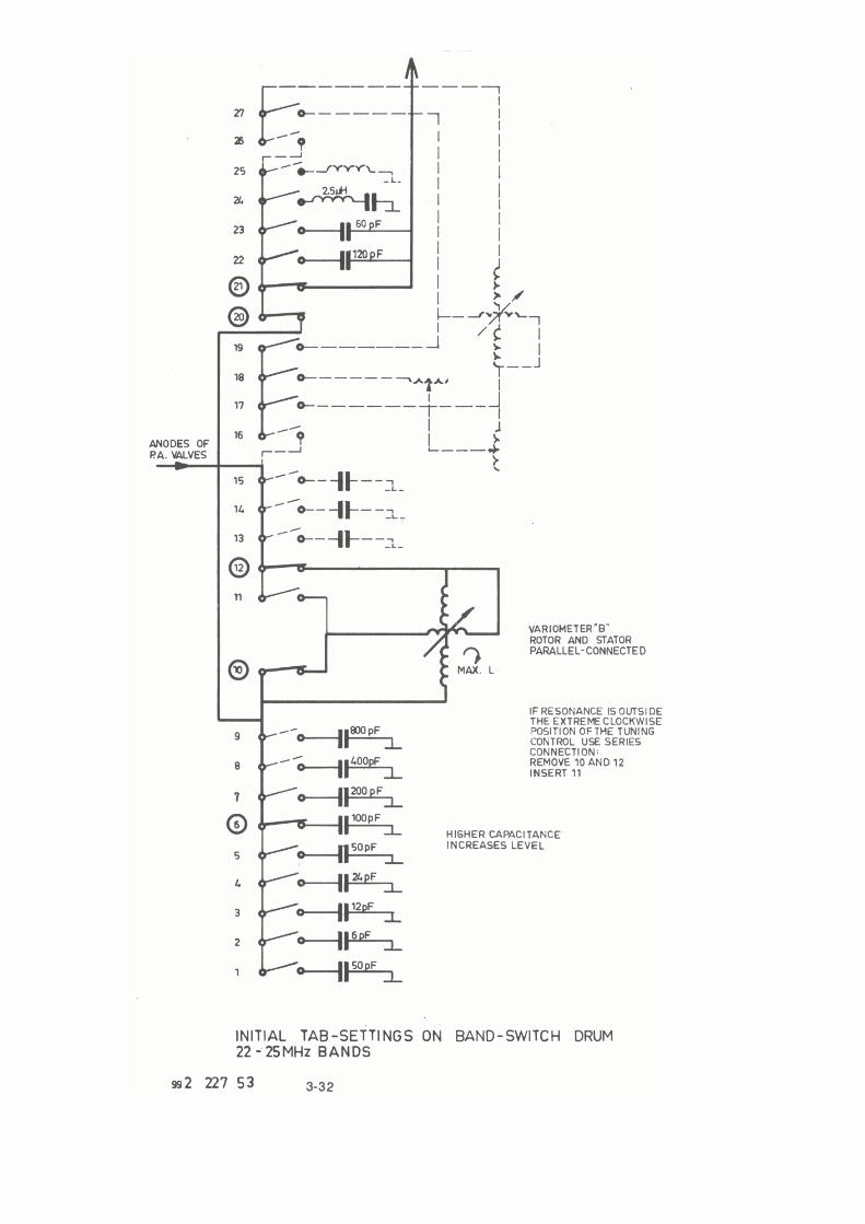
The configuration is basically, a 27-network. The series inductance may
consist of either variometer –A- or variometer -B-. The rotor and
stator of variometer -B- may be connected either in series or in
parallel. The parallel connection is to be used only in the higher
frequency bands. The transition frequency depends on the antenna.
The shunt capacitance, in parallel to the P. A. valves, is pre-set on
each band by means of wafers 13, 14, end 15.
The output capacitance can be selected between 6 and 1600 pF by means
of wafers 1 to 9. increasing the output capacitance, while still having
resonance, increases the voltage swing on the P. A. valves and vice
versa.
On frequencies above 8 MHz the output capacitance can be reduced, it
necessary, by means of the coils at wafers 24 and 25. The coil at after
24 is to be used only on the 22 MHz and 25 MHz band’s, where the
impedance of the series connected capacitor, is negligible. Due to un-avoidable stray capacitance’s, resonance in variometer –A-
can occur on one or more of the short wave band’s. It shows up as a
sudden dip in the ANTENNA CURRENT meter-reading when the TUNING control
is rotated slowly over its range. Such resonance’s within a band must
be avoided as they can cause flash-over. This is avoided by showing
variometer -A- of the band in question by inserting tabs in wafers 27
or 17 and 19 or all three.
3.14.4 Adjustment Procedure:
3.14.4.1 1.Set SUPPLY switch to STAND BY and POWER switch to MEDIUM POWER
SIMPLEX.
2. Insert tabs for the band in question as shown on Pages 3-28 to 3-32. 3. Set SUPPLY switch to TRANSMIT and press TUNE button while rotating
the TUMNG control until resonance is obtained, i.e. maximum
deflection on ANTENNA CURRENT meter without being at the extreme of
the tuning range (inspect rotor position of the variometer used).
3 - 18

4. Set CHECK SWITCH to LEVEL and pull the knob while pressing the TUNE
button. Observe Level-reading on meter. Reading should be as near 3
as possible but never above.
5. Set SUPPLY switch to STAND BY and adjust Level by selecting
appropriate tab settings on wafers 1 to 9 (refer to sections 3.14.2
and 3.14.3). Revert to point 3.
3.14.4.2 If resonance is obtained at, or is outside, one of the extreme
positions of the TUNING knob, select another variometer configuration.
3.14.4.3 If resonance cannot be obtained, remove tab on wafer 21 and insert one
or both of the shortening capacitors (wafers 22 and 23), always use the
largest possible capacitance.
3.14.4.4 If on bands A to H resonance still cannot be c>btained, insert the
output capacitor (wafer 24), if necessary in combination with one or
both of the shortening capacitors.
3.14.4.5 If Level-reading is too high, even with none of the capacitors l to 9
connected, insert the coil at wafer 25 on the 8,12 or 16 MHz bands, or
the coil at wafer 24 on the 22 or 25 MHz bands.
3.14.4.6 If flash-over occurs on 22 MHz at contact 25, insert tab in wafer 25.
3.14.5 2182 KHz:
The adjustment is performed as described above for a frequency in the
lower CT band. In order to reduce the range of the TUNING control
proceed as follows:
1. Move tab on wafer 19 to wafer 18.
2. Place one end of the clip-on lead on the middle of »2182 KHz Fine
Tuning Coil«.
3. With the other end of the clip-on lead, select that winding on the stator of Variometer »A« or the »2182 kHz Coil«, below, which gives
the highest level reading.
4. Rotate TUNING control to it se enter position and select that winding on the"2182 kHz Fine Tuning Coil" which gives maximum Level-reading.
3 - 19

MOUNTING OF TRP 5000
3 – 21

TRP 5000 CABINET, STANDARD VERSION

3 – 22

TRP 5000 CABINET, ALL OPTIONAL TERMINALS STRIPS INSTALLED
3 - 23

TRP 5000
CABINET WIRING
TERMINAL STRIP A
(mounted on cabinet back wall)
b Blue
be Beige
bk Black
bn Brown
g Green
or Orange
p Pink
r Red
s Slate (grey)
v Violet
w White
y Yellow
tt transparent
Note 1: Max cable length
to battery
Minimum
conductor size
5 Meter 2 x 10 mm2
9 meter 2 x 16 mm2
13 meter 2 x 25 mm2
NOTE 2
AN AUDIO POWER OF 5 WATTS IS AVAILABLE INTO A,40 OHMS LOAD.THIS POWER CAN BE SHARED BETWEEN SEVERAL LOUDSPEAKERS IF S0 DESIRED. THE BUILT-IN SPEAKER IN THE POWER PACK HAS AN IMPEDANCE OF 80 OHMS. WHEN CONNECTING, REMOTE SPEAKERS THE MINIMUM VALUE OF THE TOTAL IMPEDANCE SHOULD BE MORE THAN 4OHMS INCLUDING THE BUILT-IN SPEAKER IN ORDER TO OBTAIN MAXIMUM POWER OUTPUT. IF 5 WATTS IS REQUIRED IN REMOTE SPEAKER(S) THE BUILT-IN SPEAKER MUST BE DISCONNECTED. 991 202 73 3 – 23

TRP 5000
OUTPUT TERMINAL STRIP B
OPTIONAL
(Terminal strip to be mounted on cabinet back wall)
3 – 24

TRP 5000
INPUT TERMINAL STRIP C
OPTIONAL
(Terminal strip to be mounted on cabinet back wall)

3 - 25


Installation of external antenna relay for integral receiver (simplex one
antenna installation) or extra receiver.
3 – 27


T 5000 TUNING CHART
Ship : ________________________ Harbour: ___________________________________
Technician : Date: T 5000 serial no.: ________
Supply voltage : V DC/AC-50/60Hz Antenna: _______________________
CHECK SWITCH readings are taken with POWER switch in position FULL POWER DUPLEX
and MODE switch in position A3J
CHECK
SWITCH
TUNE
button not
pressed
TUNE button
pressed
VA
VS1
VS2
VG
I1
I2
VD
Freq. KHz (not 2182):
Level readings are taken with POWER switch in position MEDIUM POWER SIMPLEX and
Tune button pressed. ANTANNA CURRENT readings are taken with POWER switch in
position FULL POWER SIMPLEX and TUNE button pressed. Readings are taken on that
frequency in each band wich gives the highes Level reading.
Mark in plan below positions an drum switch in witch programming tabs have beenn
inserted.
Band
Freq.KHz
LEVEL
Ant.
Cur-
rent
1 2
3
4
5
6
7
8
9
10
11
12
13
15
16
17
18
19
20
21
22
23
24
26
27
2182 ----
A
B
C
D
E
F
G
H
4MHz
6MHz
8Mhz
12MHz
16MHz
22MHz
25MHz

992 230 0 2 3 - 33

PROGRAMMING WORK SHEET.
Transmitting
Frequency (KHz)
Frequency
Correction (KHz)
Freq.
No.
Band Mode Synthesizer
Frequency (KHz)
992 221 71 3 - 34

4. Technical Data
Modes of operation
Duplex, semi-duplex and simplex A3A, A3H, A3J, and Fl.
Semi-duplex and simplex Al and A2H.
At 2182 kHz A3H simplex only
Power Output
Al, A2H, A3A, and A3J: 400 watts Peak Envelope Power
Fl: 250 watts
with reduction to less than 20 watts.
Operating frequencies
2182 kHz plus up to 256 synthesised frequencies. The frequencies can be freely
distributed in the maritime mobile bands up to 27.5 MHz.
Frequency Accuracy Better than ± 40 Hz
Frequency Stability
Better than ± 20 Hz in any 15 minute period.
Modulation characteristic.
Within 6 dB from 350 Hz to 2700 Hz
Alarm Generator
A two-tone alarm generator is incorporated.
Supply Voltage
24 V battery with P5000 Power Pack or 110/115/120 or 220/230/240 V single, or
two phase AC, 50-60 Hz with P5001 Power Pack.
Supply Voltage Variations
DC: - 10 to + 30%
AC: ± 10%
Consumption
24 V battery AC mains
RECEIVE ONLY
STAND BY
TRANSMIT (un-keyed)
A3J (un-modulated)
A3H (un-modulated)
TRANSMIT ALARM
Fl
Al (50% duty cycle)
2.5 A
6.5 A
9 A
27 A
34.5 A
39.5 A
36.5 A
35 A
85 VA
235 VA
270 VA
800 VA
1000 VA
1200 VA
1150 VA
1150 VA
Dimensions and weight
Height (cabinet only): 822 mm
With (cabinet only): 533 mm
Depth (cabinet only): 334 mm
Weight (DC): 83.5 kgs
Weight (AC): 89.5 kgs

4 - 1
5. Technical Description
5.1 Mechanical
5.1.1 The equipment consists of four main units: Transmitter Power Amplifier,
Power Pack, Exciter and Receiver. The Transmitter Power Amplifier is
built on an alodine treated aluminium chassis. The other units are built
on zinc plated and passivated iron chassis.
5.1.2 The cooling of the two P.A. valves is by forced air, provided by a blower
installed at the back of the Transmitter Power Amplifier chassis. The
air-intake is on the front panel where an air filter is mounted. The
filter element can be removed for cleaning.
5.1.3 The transmitter power amplifier T5000 contains four printed circuit
boards. The boards /251\ and /254\ become accessible after removal of the
lid of the tube compartment at the back of the chassis./252\ is mounted
on the CHECKSWITCH and /253\ becomes accessible after removal of the
front plate.
5.1.4 The Exciter E5000 contains five plug-inboards /234\ to /238\ and two
boards in separate screened cans /232\ and /238\ that become accessible
after removal of the respective lids. Board /239\ is mounted behind the
front panel. This board and the motherboard /231\ become accessible when
the front panel is tilted forward, this is possible after removal of the
two upper screws in each side fixing the front panel.
5.1.5 The 24V DC power pack P5000 contains four printed circuit boards /261\ to
/264\. The boards /261\ and /262\ are mounted below the chassis, while
board /263\ and /264\ are mounted on the back of the chassis front plate.
5.1.6 The AC power pack P5001 contains three printed circuit boards /266\ to
/268\. The boards /266\ and /267\ are mounted below the chassis, while
board /268\ is mounted on the back of the chassis front plate.
5.2 Circuit Description, General
Each printed circuit-board and also the chassis-mounted components, have
been allocated an identification number:
Exciter, E5000, /230\ to /241\
Transmitter Power Amplifier, T5000 /250\ to /254\
Power Pack, P5001 /260\ to /264\
Power Pack, P5001 /265\ to /268\
The designation of a component or terminal includes this number as a
prefix, e.g. 232R3 (resistor R3 on board /232\), or 232-12 (terminal No.
12 on board /232\.
For convenience in this section and on the circuit diagrams, the prefix
is omitted except where there is a risk of ambiguity.
5 - 1

5.3 Circuit Summary, Exciter E 5000
5.3.1 The circuit diagram is divided into a wiring diagram on page 8-67
showing the Motherboard /231\ and the interconnections between the
printed circuit boards, of which the Exciter is composed, and circuit
diagrams of the individual circuit boards. The block diagram on page 8-
60 illustrates the operation of the Exciter.
5.3.2 The signal path is contained on boards /232\ and /232\. The AF input
signal, after having passed an input selector and a compressor, is
converted to a 1,4 MHz (or 1,973 MHz) double side-band signal by mixing
with a 1.4MHz (or 1,973 MHz) signal derived from the master oscillator.
The upper side-band is removed in a crystal filter and the lower side-
band is applied to an amplifier, the gain of which is set in accordance
with the mode selected. At the output a 1.4MHz signal of appropriate
level for carrier re-insertion is applied in the modes A3A and A3H.
5.3.3 The 1.4 MHz (or 1,973 MHz) single side-band signal is fed to the RF
Translator /233\ that converts it to the desired transmission frequency.
The 1st mixer converts the signal to an upper side-band signal in the
range 1.6 to 4.3MHz, a low-pass filter removes the image frequency. The
gain of the amplifier following the filter can be controlled in steps
from the POWER-switch. The level setting circuitry at the output of the
amplifier allows the level to be set independently at each band.
The 2nd. mixer converts the signal to the different bands by mixing it
with fixed injection frequencies. The mixer is followed by switchable
band pass filters and an amplifier.
5.3.4 In the Al,A2 Hand TRANSMIT ALARM modes the AF signal is supplied from
the tone generators on board /234\. The 1.5kHz oscillator is used for
generating the carrier frequencies in the modes Al and A2H. A 1.5 kHz
shift command from the mode control circuit makes the synthesiser
decrease its output frequency by 1.5 kHz in these modes which means that
the output frequency of the exciter be comes the correct transmission
frequency. The 2.2 kHz oscillator in addition is used for generating the
side-band intheA2H mode giving a modulation frequency of 700Hz.
The Key-line output from the keying circuit to the Power Pack tells the
HT converter to start when the line goes high. However, this is
inhibited until the phase locked loops of the synthesiser and the
Harmonic Generator have locked or if an invalid frequency No. has been
selected. If the 1.4 MHz Reference Signal is missing, the key-line is
also inhibited, as the synthesiser cannot lock.
5.3.5 The Frequency Synthesiser, contained on board /236\ and /237\, consists
of a single loop using the so-called Side-step-technique. The loop is
able to generate any frequency from 3,000.0KHz to 5,999.9KHz in steps of
100Hz. In the Fl, Al, A2H modes the output frequency is automatically
decreased by 1.5KHz.
The Frequency Synthesiser loop is locked to a l KHz reference signal
derived from the 1.4 MHz reference frequency, so that the output
frequency will exhibit exactly the same stability as the master
oscillator . The output frequency of the loop is controlled from the
Memory /238\.
5 – 2

The Side-step principle is performed as follows. Assume that the output
frequency of the Frequency Synthesiser is (a.b.c.d.,e) KHz. Th is
frequency is divided by (abcd + 1)e times and (abcd) * (10-e) times, so
that the division ratio on the average is: ((abcd + 1)* e + (abcd)*(10-
e)) = abed.e. Thus the average output frequency of the variable counter
chain will become equal to the 1 KHz reference frequency of the loop, as
it should, if the loop is properly locked.
5.3.6 The injection frequency to the 2nd. mixer of the RF Translator is
supplied by the Harmonic Generator /235\. The frequencies are all
harmonies of the 1.4 MHz (or 1,973 MHz) reference frequency. The desired
harmonic is selected by a Band Selector control- led from the Memory.
The Band Selector also selects the correct band-pass filter and level
setting potentiometer of the RF Translator.
The Memory /238\ in which the necessary information associated to each
frequency No. is stored controls the synthesiser and the Harmonic
Generator, and supplies information to the Band indicator of the
Transmitter Power Amplifier. The memory address is selected from board
/239\ which contains the keyboard and a display showing the selected
Frequency No.
The 1,4 MHz (or 1,973 MHz) reference frequency is normally supplied from
the master oscillator of the receiver. However, if the receive r is not
installed in the cabinet, Master Oscillator /240\ (or /240a\ is
available for mounting in the Exciter.
5.4 Circuit Description, Exciter E 5000 or E 5001
5.4.1 /232\ 1.4 MHz (or 1,973 MHz) EXCITER
The AF input signals are connected to the compressor through an input
selector. The microphone and line inputs are open only if the terminals
4and 8 are both HIGH. The telex AF input is open only if terminal 8 is
LOW. The tone input is always open.
The gain of the compressor is controlled by means of the field effect
transistor TR2, which functions as a variable emitter resistor for the
left hand transistor in IC1. The control voltage is provided by a
rectifier consisting of the pair of ICI transistors to the right, which
detect the side-band level at the output of the crystal filter X1. When
terminal 4 is LOW the compressor is off, as the resistance of TR2 is
kept at its maximum value.
The compressed audio signal and a 1.4MHz (or 1,973 MHz) signal from the
carrier level regulator IC2 are fed to the balanced mixer IC3. The
output is a 1.4MHz (or 1,973 MHz) double side-band suppressed carrier
signal, which is amplified in TR4 and fed through crystal filter X1 that
removes the upper side-band and suppresses the carrier still further.
The gain of the amplifier stage following the filter is controlled from
terminals 13, 14, and 15 by inserting different emitter resistors. In
the A3H-rnode all terminals are HIGH and the gain is determined by R70.
Carrier re-insertion is performed by applying the 1.4MHz signal from the
carrier level regulator to TR6 via an attenuator controlled from the
same terminals.
5 – 3
5.4.2 /233\ RF TRANSLATOR
The lst. mixer converts the 1.4 MHz (or 1,973 MHz for LSB) LSB-signal to
an USB-signal in the frequency range 1.6 to 4.3 MHz, by mixing it with
the injection frequency from the VCO of the synthesiser. The image
signal is removed in the 4.3MHz low-pass filter and the wanted signal is
applied to TR1. The gain of this stage is controlled from the POWER
switch via terminals 1 and 2. The load-resistance at the collector is
adjustable and can be set individually at each band by means of variable
resistors.
The 2nd. mixer converts the signal to the transmission frequency. The
injection frequency is fixed for each band. In the bands 1.6 to 4 MHz
and the4 MHz HF band the injection frequency is zero, which means that
the output frequency is the same as the input frequency. The mixer works
as an amplifier since the one pair of transistors are cut off by means
of Dl 1 or 01 2.
The mixer is followed by a number of band pass-filters and an amplifier.
A filter is selected by taking one of the terminals 12 to 21 LOW, while
keeping the others HIGH. At the same time the corresponding level
setting potentiometer is selected.
5.4.3 /234\ CONTROL CIRCUIT AND TONE GENERATORS
The mode control signals from the MODE-switch, and the 2182 khz and MF
information from the transmitter power amplifier, are the input signals
to the programmable Read Only Memory (PROM), IC5, of the Mode Selector.
The PROM has been programmed to give at the output the desired control
signals corresponding with the wanted mode.
The Mode Selector controls the input selector and the mode setting of
the 1.4MHZ (or 1,973 MHz) Exciter /232\ via the respective control
leads. The 1.5 kHz SHIFT output. tells, when HIGH, the synthesiser to
decrease its frequency by 1.5 kHz.
In the Fl-mode, the anode voltage of the P.A. valves is lowered by means
of are lay in the Power Pack controlled from transistor TR5. Automatic
selection of FULL POWER is carried out by means of transistor TR4, when
2182kHz (terminal 14a LOW) and TRANSMIT ALARM (output 06 of IC5 LOW) are
selected. The mode selector further controls the Key Selector.
Keying of the transmitter is only possible from the MORSE KEY input in
the A2H and Al modes, from the TELEX KEY input in the F1 mode, from the
HANDSET KEY input in the A3A, A3J, A3 Hand TRANSMIT ALARM modes, and
from the DUPLEX input in the Fl, A3A, A3J, A3H or TRANSMIT ALARM modes,
provided 2182 kHz is not selected, as the DUPLEX input is then
inhibited. Furthermore the information on terminal 24a (WT) from MEMORY
/238\ has to be in accordance with the mode selected (except on 2182
kHz): HIGH at A2H, Al, and Fl, LOW at A3A, A3J, A3H, or TRANSMIT ALARM.
The keying signal at IC2, pin 8 controls, via an inverter, transistor
TR9, supplying +12V to RF TRANSLATOR /233\ when keyed, and activating
the key-line to the power pack. In SIMPLEX it supplies base current to
TR8, controlling the muting of the receiver.
The Two-tone Alarm Signal Generator incorporates the 45 sec. Timer, the
2Hz Astable Multivibrator, and the 2.2 kHz and 1.3 kHz Oscillators. The
45 sec. Timer is enabled from the Mode Selector in
5 – 4

TEST ALARM and TRANSMIT ALARM, and can be started by pushing the ALARM
START push-button that applies +12 V to terminal 2c. Via the voltage
divider R32 and R33, a keying signal is applied to the Key Selector. The
2Hz Astable Muitivibrator starts and supplies base current to TR6 and
TR11 alternatively. The audio signal from the oscillators is, via the
Tone Keyer, applied to the l.4MHz EXCITER /232\ and, via the Side Tone
Keyer, applied to the receiver audio amplifier.
In the Al-mode the 1.5 kHz oscillator is started. The audio signal is
keyed in the Side-tone Keyer and the Tone Keyer which are both
controlled from the morse key. Capacitor C8 and adjoining components at
the gain control input of IC7 serve to shape the tone pulses correctly.
In the A2H-mode, the 2.2 kHz oscillator as well as the 1.5khz oscillator
are on. R54 is connected to ground in IC4, thereby reducing the peak
level of the audio signal at the Tone Keyer input to the same level as
when only one tone is present. The Side-tone Keyer is connected to the
1.5 kHz oscillator only, as TR12 is turned off by means of D24.
When the TUNE-button of the Transmitter Power Amplifier is activated,
terminal 18c is LOW. A2H is selected by means of Dl and D3, the
transmitter is keyed via IC2 pin 9, and the Side-tone Keyer is turned
off by means of IC,9 pin 1.
5.4.3 /235\ HARMONIC GENERATOR
There is one phase looked loop and its associated lock detector located
on this printed circuit board.
The reference frequency of 1.4 MHz for this loop is derived from the
TCXO, in order to accomplish the necessary degree of frequency stability
of the output signal from the Voltage Controlled Oscillator.
The fixed reference frequency of 1.4 M Hz is fed to one of the two input
ports of the Phase / Frequency Detector. The output from the loop
Divider is fed, via IC2, to the other input port of the Phase /
Frequency Detector, which in the case of a frequency difference between
the two signals will produce a DC-error voltage.
The purpose of the Low Pass Filter is to remove the pulses from the
output of the Phase/Frequency Detector, thus allowing only the DC-error
voltage to pass on to the vari-cap diodes of the Voltage Controlled
Oscillator.
The outputs of the VCO are amplitude regulated and fed to the RF-
TRANSLATOR /233\ and Pre-scaler respectively.
The division ratio of the Pre-scaler and the Loop Divider is controlled
by four outputs of the Band Decoder, IC4, which is again controlled by
the BAND-information stored in the MEMORY /238\.
Four other outputs of the Band Decoder select, via the Band Selector
IC1, the proper band of the VCO and the proper band pass filter of the
RF TRANSLATOR /233\.
The Lock Detector detects any frequency difference between the two
signals fed to the input ports of the Phase/Frequency Detector. When a
frequency difference is observed, the Lock Detector turns on TR9, thus
pulling down the KEYLINE to a low level voltage, as long as frequency
equality is not accomplished.
5 - 5

5.4.5 /236\ VCO
The Loop Filter and Voltage Controlled Oscillator are located on this
printed circuit board.
The Loop Filter consists of an active4th order low pass filter and an
integrator. The purpose of the Loop Filter is to remove the pulses from
the output of the Phase/Frequency Detector on board /237\ and allow only
the DC-information to pass on to the vari-cap diodes of the VCO. The VCO
is amplitude stabilised.
The selection of one of the three bands of the VGO is carried out by
means of a decoding circuit on /237\.
5.4.6 /237\ FREQUENCY DIVIDERS A
There are two divider chains, their associated buffer amplifiers, a
2182KHz pre-selection circuit, a lock detector, and a phase 1 frequency
detector located on this printed circuit board.
The Reference Divider divides the 1.4 MHz from the TCXO by 1400, thus
providing the 1KHz reference frequency for the Phase/Frequency Detector.
The Loop Divider chain consists of four programmable, decimal counters,
IC16, IC20, IC23, and IC26, which are loaded at the end of each counting
cycle with the data blocks supplied by the Memory /238\ or the 2182 kHz
Pre-selection circuit. The Side-step Control consists of a decimal
counter, IC6, a four bit comparator, IC10, and gating circuitry. A data
block, containing the information about the 100 Hz setting is fed to the
comparator. At the end of each counting cycle IC6 is incremented by one
and its outputs (B) are compared with the content of the data block (A).
As long as B is less than A the division ratio of the four programmable
counters are equal to the BCD 9’s complement of their four associated
data blocks. When B becomes equal to or greater than A the division
ratio is incremented by one. This change of the division ratio is
controlled by output pin 5 of IC10, which selects one of the two
decoding branches, branch 1 and branch 2, consisting of parts of IC3,
IC4, ICS, and IC8, and one half of IC1.
When the mode Fl, Al, or A2H is chosen, the division ratio is decreased
by one and two alternately, independent of the above mentioned side
stepping procedure. This is controlled by the "1.5 kHz SHIFT" line and
performed by the other half of IC1, where output pin 9 is changed at the
conclusion of each counting cycle, thus shifting between the two
decoding branches, branch 3 and branch 4, alternately. This means that
the division ratio is decreased by 1.5 on the average. Because the
reference frequency of the loop is 1 kHz, this means that the output
frequency of the loop is decreased by 1.5 kHz.
The output from the Loop Divider chains fed to the Phase / Frequency
Detector and is here compared to the fixed l KHz reference frequency. In
case of a frequency difference the detector will produce a DC-error
voltage which will correct the VCO en board /236\ to establish the
wanted frequency equality.
The two inputs /238\ -9a and /238\ -10a containing information about the
MHz setting is decoded in order to select the proper band of the VCO on
board /236\. If both of the two inputs are HIGH, the Disable output line
is activated.
5 - 6

The Look Detector consists of IC15 and IC17. If the loop is in look,
output pin 9 of IC19 will always be L0W when the output pulse from the
Loop Divider is generator, so output pin 9 of IC15 stays LOW.
In an unlocked condition of the loop, output pin 9 of IC19 will be at a
LOW or HIGH logic level at random when the output pulse from the loop
Divider is generated. The first mono-stable multivibrator of IC17 is
triggered by the corresponding output changes of IC15, thus, via the
last half of IC17, inhibiting the Keyline.
If the reference signal of the loop is missing, this is detected by the last half of IC17, again inhibiting the Keyline.
5.4.7 /338\ MEMORY
This printed circuit board contains 24 sockets, organised as eight
columns (No. one to No. eight) by three rows (A, B, and C). Thus up to
24 Programmable Read Only Memories (PROMS) corresponding to 256
different Frequency Nos. can be mounted in the MEMORY.
The PROM used here is organised as 32 words by 8 bits. Because 24 bits
are needed as control information for each Frequency No. three PROM’s
must be driven in parallel, corresponding to an extended memory block
organised as 32 words by 24 bits.
A memory block consisting of three PROM’s is mounted in one of the eight
columns. The PROM’s in column No. one contain the necessary 24 bits
associated with the Frequency Nos. from 0 to 31, column No. two contains
the 24 bits associated with the Frequency No’s from 32-63 and so on (see
table 3.12.1).
From board /239\ the binary encoded Frequency No. selects, via 5/6 IC1,
one of 32 words and, via IC2, one of eight columns.
5.4.8 /339\ DISPLAY AND KEYBOARD
When a key is depressed the associated key-number is encoded to the BCD
code by means of IC2 and IC4. This BCD coded data block is fed to the
input ports of the first register IC8 of the Digit Register Stack.
When a key is depressed or released some sort of bouncing effect will
always appear before the key has settled. This bouncing is removed by
means of the Key Bounce Eliminator, consisting of IC5 and the associated
extern at components. A clock pulse is produced when the key has
settled, after being activated, and then the data block mentioned above
is read into the first register of the Digit Register Stack, and the
data blocks already stored in this Stack are shifted to the next
register. The outputs of the Digit Register Stack are the BCD code of
the Frequency No. chosen. Via the three BCD to 7-segment decoder-
drivers, IC12, IC14, and IC19, the Frequency No. is displayed. The BCD
encoded Frequency No. is converted to its associated binary code before
it leaves this board, by means of IC15, IC16, IC20, and IC21, in order
to select the proper information stored in the Memory /238\. ]t is not
possible to choose a Frequency No. greater than 255, if such an attempt
is done a decoding circuitry of 3/4 IC7 automatically clears the Digit
Register Stack.
By means of the variable voltage regulator consisting of TRI, TR2, and
associated components the three Led-displays can be dimmed continuously.
5 – 7

When the BAND switch is turned into the 2182 kHz position, terminal 11
receives a LOW level signal which, via 3/4 IC6, activates the ripple
blanking outputs of IC12, and IC19. The displays are then blanked, but
the original Frequency No. is stored.
If a HIGH level is applied to terminal 13 (Disable) or a LOW level to
terminal 14 (Programmed Frequency No.), the Blanking Oscillator
consisting of IC3 and associated components starts a 1Hz oscillation and
the Key-line is inhibited. Thus the displays, via 3/4 IC6 and IC12,
IC14, and IC19, will start to flash with a frequency of 1 Hz. However,
if the BAND switch is turned to its 2182 kHz position, the levels of
terminals 13 and 14 do not affect the Key-line.
5.4.9 /240\ MASTER OSCILLATOR
The oscillator itself is a sealed unit containing a highly stable
temperature compensated crystal oscillator, TCXO, at 11.2 MHz. The
output signal of the TCXO is amplified in the transistors TRI to TR3 and
fed to the binary counter IC1 that divides the input frequency by 8. The
1.4 MHz square wave signal is filtered in a tuned Circuit C6, T1, and
the re-suiting sine wave signal is fed to the output terminals.
TCXO's of two different manufactures may be used. In both cases crystal
oscillator ageing is very small (less than 10-11 per anum)and will be
greatest during the first few years. Ageing will normally cause an
increase in frequency, which in the one case can be compensated for by
introducing the connection indicated by the dotted line in the circuit
diagram (this will reduce the frequency by approx. 2*10-6) and in the
other case by changing the factory selected resistor.
The resistor should be selected at 25°C ambient temperature to give a
TCXO output frequency offset from the nominal frequency (11.2 MHz) by
the amount marked on the can.
Frequency adjustment should be carried out only if a high quality coun-
ter is available for control of the frequency. It must be ensured that
the accuracy of the counter at the time of use is better than 10-7.
5.4.10 /241\ PROGRAMMING UNIT (Optional)
The purpose of this printed circuit board is to make it possible to
program manually the PROM’s used as building blocks in the MEMORY /238\.
The only types of PROM’S, which can be programmed by means of the
PROGRAMMING UNIT are the TI-types shown in table 3.11.1. Three PROM’s
together can contain the information of 32 different Frequency No’s. The
three PROM’s are placed in SK1, SK2 and SK3. Their input word address is
chosen by means of the key-board on the front panel, thus selecting
one of the 32 possible words in each of the three PROM’S.
A programmed output will be greater than 2V (HIGH), an un-programmed
output will be less than 0.8V (LOW). To prevent an attempt being made,
by mistake, to program new information into a word which has already
been programmed once, one bit location, pin 9 of the PROM placed in SK1,
must always be programmed if the rest of the bit locations of a
Frequency No. have been correctly programmed.
Half of IC4 is always sensing the voltage level on pin 9 of SK1. If this
voltage level is HIGH, pin 5 of IC4 will also become HIGH after the
first positive transition of the clock pulse at pin 3, thus disabling
IC2 and thereby IC6 and IC8 from being activated by the key S1.
5 - 8

By activating the key S2, the output of pin 9 of SK1 will be forced LOW,
as for an un-programmed Frequency No., thus permitting the user via the
key S1 to activate IC and there by IC6 and IC8.
Their outputs are combined by means of 4/6 IC5, 2/4 IC7 and 1/4 IC3 into
three pulse-trains, one for the Vcc-pins and one for the Enable pins of
the three PROM’s and lastly one for the transistor TR1. This transistor
sinks the programming current from the PROM-output to which the
Programming Pin is connected.
The three pulse-trains are shown below.
The two voltage levels of the Vcc-pins of the PROM’s are stabilised by
means of D3 and IC9.
In order to keep the PROM’s as cool as possible, which is very essential
to obtain good programming re-suits, their Vcc supply line only receives
a 5V pulse in 5msec out of 100msec during the period of time where no
programming takes place. This pulsed operation is controlled by a clock-
pulse generated by IC1 openin,0 and closing, via 214 1G3 and 216 ICS,
the transistorTR2.
At the end of each 5msec period the logic levels of pin 9 of SK1 and the
Programming Pin are read into the two D-flipflops of IC4; a HIGH level,
corresponding to a programmed bit location will make the associated lamp
light.
When the key SK1 is activated and MON1 of IC2 is triggered, the clock
generator IC1 is stopped. Once the programming pulse-trains have been
accomplished the clock generator is allowed to start again after a delay
of approximately 30msec.
A delay circuit consisting of R71, R72, C12 and D4 prevents the Vcc-
programming pulse from being generated when the PROGRAMMING UNIT is
first switched on. This prevents false generated signals to IC2. This is
accomplished by turning off TR2 via 1/4 IC3 and 2/6 IC5 until all the
voltage levels have stabilised.
5 – 9

5.5 Circuit Summary, Transmitter Power Amplifier T 5000
5.5.1 The circuit diagram is divided into a wiring diagram On page 8-89
showing the interconnections between the printed circuit boards of which
the Transmitter Power Amplifier is composed, and circuit diagrams of the
individual circuit boards. The block diagram on page 8-61 illustrates
the operation of the Transmitter Power Amplifier.
5.5.2 The RF signal from the Exciter is amplified in the DRIVER /251\ and
applied to the P.A. output valves. Antenna tuning is pre-selected with
the BAND switch, and fine tuning is performed with the TUNING control.
5.5.3 Antenna current measuring and CHECK SWITCH circuits are contained on
printed circuit board /252\.
5.5.4 Visual indication of whereto set the BAND-switch in accordance with the
frequency selected is performed by the BAND INDICATOR /253\. When
2182kHz is selected, information is supplied to the Exciter. If the BAND
switch is incorrectly set, the Key-line inhibit output prevents keying
of the transmitter.
5.5.5 Regulation of grid and screen grid voltages, as well as filament
voltages f or the P.A. output valves, is carried out on printed circuit
board /254\.
5.5 Circuit Description, Transmitter Power Amplifier T5000 DRIVER
5.6.1 /251\ DRIVER
A preamplifier consisting of TR1 and TR2 in parallel amplifies the
signal which is then applied to a class-a push-pull stage consisting of
the transistors TR3 and TR4. The DC current of these transistors is set
by means of the variable resistor R7. Coarse setting is by means of the
resistors R13-R15. The compensation network at the output provides a
flat response over the frequency range.
5.6.2 /252\ METER CIRCUIT
The printed circuit board is an integral part of the CHECK SWITCH and
contains voltage dividers for metering different voltages of the
transmitter Power Amplifier. Dl rectifies the current of the antenna
current transformer. D2, R11, and R13 provide compression of the meter
scale. TR1 inverts the negative grid voltage to a positive current in
the meter when checking VG.
5.6.3 /253\ BAND INDICATOR
The purpose of the Band Indicator is to show where to set the BAND
switch in accordance with the frequency selected. This is done by means
of 16 light emitting diodes, 15 of which are controlled from two 1 of 10
decoders IC3 and IC5. These decode the binary band information from the
Exciter and make one of the lamps flash if the BAND switch is
incorrectly set. The BAND switch information and the information from
the Exciter are compared in the Comparator, IC4. If they are not equal
the output will be LOW and will via lC6and IC7, start the 1Hz
Muitivibrator (FLASH ENABLE: HIGH) that controls the decoders via 2/4
IC1. At the same time the Key-line output is LOW thus inhibiting
transmission.

5 – 10

When "2182 kHz" is selected by means of the BAND switch the information
is HIGH on al] four input leads from the BAND switch. In that case the
output from 1/2 IC2, pin 8, is HIGH and as terminal 7 is open and thus
HIGH too, the output of 1/4 IC1, pin 11, is LOW, telling the Exciter to
select 2182 kHz. The light emitting diode Dl will show constant light.
5.6.4 /254\ VOLTAGE REGULATORS
The Grid Voltage Regulator consists of two integrated circuits IC1 and
IC2 that operate as zener diodes having a very low temperature
coefficient. The actual grid voltage is set by means of the variable
resistor R1.
The screen grid voltage of the power amplifier tube Vl is fixed and
determined by two 150V zener diodes 250 Dl and 250 D3. In order to be
able to equalise the currents of the two tubes, the screen grid voltage
of V2 is made adjustable. The zener diodes 250 D5 and 250 D6 are
connected to a voltage-regulator containing transistor 250 TR1, the
collector voltage of which can be set by means of variable resistor R3.
The 6V filament voltages of, the power amplifier tubes has to be
controlled within very narrow limits to obtain maximum tube life. This
is done in the Filament Voltage Regulator. In order to reduce current
consumption the filaments of the two tubes are series connected, which
means that the voltage of each tube has to be control- led. The
regulator of V2 consists of the NPN darlington transistor 250 TR1 in
connection with the zener diode D4 and resistor R15. When the voltage of
the filament reaches 6V, the transistor starts to conduct and shunts the
filament by which the voltage is kept constant. The regulator of V, is
identical except the transistor is a PNP darlington. The collector
currents of the two transistors pass the diodes D5 and D6, and the
voltage across these diodes is applied to a current regulator consisting
of TR1 and 250 TR2. TR3 serves to limit the peak current.
5.7 Circuit Summary, 24V DC Power Pack P5000
5.7.1 The circuit diagram is divided into a wiring diagram On page 8-99
showing the interconnections between the printed circuit boards of which
the Power Pack is composed, and circuit diagrams of the individual
circuit boards. The block diagram on page 8-62 illustrates the operation
of the Power Pack.
5.7.2 Filament supply for the transmitter power amplifier output valves is
obtained directly from the battery, while the remaining necessary supply
voltages for transmitter Power Amplifier, Exciter and Receiver are
generated in converters. Converter transformers give full isolation
between the battery voltage and the chassis, permit- ting these to be
earthed without causing the supply leads to be earthed.
5.7.3 Low tension voltages for Exciter and Receiver and negative grid voltage
for the Transmitter Power Amplifier are generated by the LT-converter
followed by rectifiers and stabilisers.
The LT-converter frequency is determined by an RC-coupled oscillator
followed by a bi-stable muitivibrator.

5 - 11

5.7.4 High tensions for the P.A. valves are generated by the HT-converter
followed by rectifiers. To avoid excessive anode voltage to the P.A.-
valves at high battery voltages an input voltage sensor is incorporated
in the power pack. When the input voltage exceeds a certain voltage a
relay in the input voltage sensor circuit will operate and decrease the
anode voltage.
Supply voltage f or the driver stage in the transmitter power amplifier
is also generated in the HT-converter followed by rectifiers and a
voltage stabiliser.
The HT-converter is driven from two secondary windings on the LT-
converter transformer.
5.7.5 To fulfil the input voltage requirements of the blower in the
transmitter power amplifier, a separate blower converter is
incorporated.
5.8 Circuit Description, 24V DC Power Pack P5000
5.8.1 /260\ LT-, HT-, AND BLOWER-CONVERTER
Relay RL1 serves as a mains switch. The current which energises RL1 is
controlled by the POWER switch. Turning the switch from OFF to RECEIVE
ONLY connects the relay coil to the battery voltage. Diode 261 Dl
ensures that the relay cannot operate if the battery voltage does not
have the correct polarity. The contacts of RL1 are protected against
excessive capacitor charging current by resistor R2. The resistor
ensures that the capacitors after the relay are always charged before
the contacts are closed.
The LT-converter is composed of transistors TR10 and TR12, and the
square-wave output signal is coupled through transformer T3 to the LT-
and grid voltage-rectifiers and as a drive signal to the HT-converter.
The HT-converter contains transistors TR4, TR6, TR8 and TR11 and the
output signal is coupled through transformer T2 to the HT-rectifiers.
The Blower-converter contains transistors TRI and TR2 and the output
transformer T1 transforms the square wave output voltage to the correct
level.
Included in the Power Pack is also a loudspeaker connected to the
associated receiver AF-output.
5.8.2 /261\ CONVERTER DRIVER LT-RECTIFIERS AND LT-STABILIZERS.
A bi-stable muiti-vibrator composed of transistors TR2 and TR4 is driven
by oscillator IC1 with a nominal frequency of 440Hz. The output signals
from the muiti-vibrator are therefore square waves with a repetition
frequency of 220Hz, and these signals having a phase difference of 180"
are, after current amplification in transistors TR1 and TR3, used as
driving signals for the LT-converter.
One output signal from the LT-converter is rectified in diodes D11 and
D12 which are followed by two voltage stabilisers both having a nominal
voltage of 7.5 V.
Another output signal from the LT-converter is rectified in diodes D16
and D17 followed by a voltage stabiliser having a nominal output voltage
of 15.7V.

The board contains also the keying relay RL1 for the complete TRP5000
equipment. The contacts of the relay are used to disconnect the speaker
built into the Power Pack, and to key the grid bias of the P.A. valves.
5 - 12

5.8.3 /262\ HT-RECTIFIERS AND BASE KEYING CIRCUIT.
The current which energises relays RL1 and RL2 passes Transmitter Power
Amplifier safety switch 250S1 and Power Pack safety switch 260S2 and is
controlled by keying relay 261RL1. Via the contacts of RL1 and RL2, base
drive is applied to the HT-converter transistors and the square wave
output is rectified in six bridge circuits. The DC-outputs of each
bridge are series connected to obtain the anode supply voltage for the
Transmitter Power Amplifier, while the DC-output from the second bridge
above ground is used as screen grid supply voltage.
When the MODE switch of the associated Exciter is set to Fl, the anode
voltage is lowered by opening the contacts of relay RL3 and thereby the
anode dissipation in the Transmitter Power Amplifier is de-creased.
The anode voltage is further controlled by relay 264RL1 which in the
case of high battery voltage will de-crease the available anode-voltage
by disconnecting the input voltage to one of the six bridge rectifier
circuits.
5.8.4 /263\ DRIVER- AND GRID-VOLTAGE STABILIZERS, BLOWER CONVERTER DRIVER AND
TIMER
An output voltage from the HT-converter transformer 260T2 is fed to
rectifiers Dl and D2 followed by a voltage stabiliser having a nominal
output voltage of 28 V.
An output voltage from the IT-converter transformer 260T3 is fed to
bridge rectifier D3, D4, DS and D6 followed by a zener diode stabiliser.
The stabilised voltage is negative with respect to chassis and is
further stabilised in the Transmitter Power Amplifier to be used as grid
voltage.
To avoid the transmitter being keyed before the filaments of the P.A.
valves have reached their operating-temperature, a 30 seconds timer is
included. The timer is composed of integrated circuit 101 and will
commence the timing period when the POWER switch 260S1 is turned from
RECEIVE only to STAND BY. Until the 30 seconds period has elapsed the
keying relay 26 RL1 con not be operated.
The blower in the Transmitter Power Amplifier requires a 50 Hz input
voltage. A bi-stable muitivibrator composed of transistors TR2 and TR4
is driven by oscillator TR1 with the nominal frequency 100Hz. The output
signals from the muitivibrator are therefore square waves with a
repetition frequency of 50 Hz, and these signals which have a phase
difference of 180˚ are used as driving signals for the Blower-converter.
5.8.5 /264\ INPUT VOTAGE SENSOR
A Schmitt-trigger having a hysterisis of approx. 2 volts is used as an
input voltage sensor. If the battery input voltage exceeds a certain
value relay RL1 will open and decrease the anode voltage by opening one
of the secondary windings on the HT-transformer 260T2. When the battery
voltage is approx. 2 volts below the trigger point relay RL1 will close,
increase the anode voltage and thereby ensure that the anode dissipation
of the P.A. valves are within safe limits.
The -board also carries a noise suppression filter for the Blower-
converter.

5 - 13

5.9 Circuit Summary, AC Power Pack P5001
The circuit diagram is divided into a wiring diagram on page 8-109
showing the interconnections between the printed circuit boards of which
the Power Pack is composed, and circuit diagrams of the individual
circuit boards. The block diagram on page 8-63 illustrates the operation
of the Power Pack.
All necessary supply voltages for Transmitter Power Amplifier, Exciter
and Receiver are obtained through transformers T1 and T2. The
transformers give full isolation between the mains input voltage and
chassis, permitting these to be earthed without causing the mains leads
to be earthed.
Low tension voltages for Exciter and Receiver and negative grid voltage
for the Transmitter Power Amplifier are obtained through transformer T1
followed by rectifiers and stabilisers.
Transformer T1 also carries secondary windings for filament supply to
the P.A. valves and for the blower in the Transmitter Power Amplifier.
High tension for the Transmitter Power Amplifier is obtained through
transformer T2 followed by rectifiers.
Supply voltage for the driver stage in the Transmitter Power Amplifier
is also obtained from transformerT2followed by rectifiers and a voltage
stabiliser. Included in the Power Pack is also a loudspeaker connected
to the associated receiver AF-output.
5.11 Circuit Description, AC Power Pack P5001
5.10.1 /265\ TRANSFORMERS
A double mechanically operated safety switch is inserted in the mains
input leads. The primary current of transformer TI is controlled by the
POWER switch. Turning the switch from OFF to RECEIVE ONLY connects the
transformer to the mains and low tension is supplied to the Receiver.
Relay RL1 connects the primary windings of transformer T2 to the mains.
5.10.2 /266\ LT-STABILISERS
One output voltage from transformer 265 T1 is rectified in the chassis
mounted diodes 265 D1 and 265 D2. Two voltage stabilisers, one supplying
the Receiver and one the Exciter, have a nominal voltage of 7.5V.
Another output voltage from transformer 265 T1 is rectified in diodes D8
and D9 followed by a voltage stabiliser having a nominal output voltage
of 15.7V. This voltage is supplied to both Receiver and Exciter.
The board also contains the keying relay RL2 f or the complete TRP5000
equipment. The contacts of the relay are used to disconnect the speaker
built into the Power Pack and to key the grid bias of the P.A. valves.

5 - 14

5.10.3 /267\ HT-RECTIFIERS A
HT-transformer 267 T2 has six secondary HT-windings. Each winding is
connected to a bridge rectifier and the DC-outputs are series connected
to obtain the anode supply voltage for the Transmitter Power Amplifier,
while the DC-output from the second bridge above ground is used as
screen grid supply voltage.
When the MODE switch of the associated Exciter is set to Fl, the anode
voltage is lowered by Opening the contacts of relay RL1 and thereby the
anode dissipation in the Transmitter Power Amplifier is decreased.
5.10.4 /268\ DRIVER AND GRID VOLTAGE STABILIZERS
An output voltage from the HT-transformer 265 T2 is fed to rectifiers Dl
and D2 followed by a voltage stabiliser having a nominal output voltage
of 28V.
An output voltage from the transformer 265 T1 is fed to bridge rectifier
D3, D4, D7 and D8 followed by a zener diode stabiliser. The stabilised
voltage is negative with respect to chassis and is further stabilised in
the Transmitter Power Amplifier to be used as grid voltage.
To avoid the transmitter being keyed before the filaments of the P.A.
valves have reached their operating temperatures a 30 seconds timer is
included. The timer is composed of integrated circuit 1G1 and will
commence the timing period when the POWER switch 265S2 is turned from
RECEIVE ONLY to STANDBY. Until the 30 seconds period has elapsed the
keying relay cannot be operated.
The board contains also a filament-voltage rectifier D5 and D6, and
relay RL1 is used to apply power to the blower in the Transmitter Power
Amplifier.

5 - 15
6. Simple Service
6.1 Incorrect Operation
If the equipment is not functioning correctly, a check should be made
that it is being operated properly. Go through adjustment procedures 2.2
and 2.3 if necessary.
6.2 Battery
The condition of the battery should be checked at frequent intervals.
The battery must always be fully charged and should be topped up
frequently with distilled water (liquid should rise 5 to 10 mm above the
plates).
6.3 Checking the Antenna Tuning
The antenna tuning may be checked by adjusting the transmitter as
described in section 2.3, preferably on one of the frequencies that was
listed in the TUNING CHART when the equipment was installed.
Then set POWER switch to SIMPLEX, MEDIUM and CHECK SWITCH to LEVEL. Pull
the CHECK SWITCH knob out and press TUNE button. Note the meter reading.
Set POWER switch to SIMPLEX, FUIL and press TUNE button. Note ANTENNA
CURRENT reading.
Compare the readings with the readings listed in the TUNING CHART. ]f
the two readings differ appreciably from the listed values, and the
transmitter is otherwise functioning normally, the fault can be expected
to be in the antenna system or in the transmitter earth connection.
Accordingly, the following cheeks should be made:
Have any changes been made in antenna or earth connections since the
installation was made?
Have any changes been made in the rigging of the vessel, or in the
placement of derricks etc.?
Is leakage present on the antenna, possibly caused by moisture or dirt
on the antenna insulators?
6.4 Using the CHECK SWITCH
The CHECK SWITCH is not normally operative. Pulling the switch knob out
will switch the ANTENNA CURRENT meter to read the voltage or current
selected with the switch. When released, the knob will return to its
original position.
The meter reading in all positions except LEVEL is approx. 3 under
normal conditions, i.e. transmitter adjusted as described in section
2.3, POWER switch set to FULL and TUNE button pressed.

6 - 1

Position of
CHECK SWITCH
Check of Deflection to
3 corresponds
to approx.
Actual deflection
VA
Vs1
VS2
VG
I1
I2
VD
anode DC voltage
screen grid voltage
of valve no. 1
screen grid voltage
of valve no. 2
control grid bias
cathode current of
valve no. 1
cathode current of
valve no. 2
supply voltage to
driver amplifier
1700
300
300
-49
165
165
28
V
V
V
V
mA
mA
V
2.4 to 3.5
dependent on supply voltage
2.4 to 3.6 dependent
on valve characteristics
2.3 to 3.7 dependent
on valve characteristics
Table 6.4.1
If the meter shows no reading in these positions, reference should be
made to section 6.5.
With POWER switch set to DUPLEX, FULL and TUNE button not pressed, valve
current readings, I1 and I2, in the A3J mode, un-modulated will be
approx. 1.4, and in the A3H mode, un-modulated approx.2.3.
6.5 Replacement of Fuses
All fuses, except the high tension fuse, are accessible on the front
panel of the Power Pack. The high tension fuse becomes accessible when
the Power Pack is pulled out.
Note: Set SUPPLY switch to OFF and open external supply voltage switch
before opening the equipment and replacing fuses. Short circuit both
ends of high tension fuse to chassis using an insulated tool before
touching it.
Fuse ratings are given in table 6.5.1 and table 6.5.2 below. Fuses with
marked ratings within 5 per cent of the ratings given must be used. Note
that slow or fast blowing fuses must be used where specified.

6 - 2

Fuse Rating Designation Front Panel Fuses
(from left to right)
Symptom if fuse is blown
1.6A fast
1.6A fast
3.15A fast
40A fast
8A fast
1.6A fast
0.5A fast
0.5A HT
260FS 5
260FS 6
260FS 3
260FS 2
260FS 1
260FS 4
260FS 8
260FS 7
7-5v to Receiver
15-7V to Receiver and
Exciter
7-5V to Exciter
24V battery input
(LT-and HT-converters)
24V battery input
(RL1, filament supply,
blower)
28V to Driver in T5000
600V screen grid
supply
no light in display
no light in displays,
negative deflection in
CHECK SWITCH position VG
no light in displays
no light in displays
no light in displays,
no cabinet light
no reading in CHECK
SWITCH position VD
no reading in CHECK
SWITCH positions Vs1
and Vs2
no reading in CHECK
SWITCH position Va
High Tension Fuse
1700V to anodes
Fuse Ratings, 24V-DC Power Pack P5000
Table 6.5.1.
Fuse Rating Designation Front Panel Fuses
(from left to right)
Symptom if fuse is blown
1.6A fast
1.6A fast
3.15A fast
8/16A slow
8A fast
1.6A fast
0.5A fast
0.5A HT
265FS 3
265FS 7
265FS 2
265FS 1
265FS 8
265FS 6
265FS 5
265FS 4
7-5v to Receiver
15-7V to Receiver and
Exciter
7-5V to Exciter
mains input
filament supply,
28V to Driver in T5000
600V screen grid
supply
no light in display
no light in displays,
negative deflection in
CHECK SWITCH position VG
no light in displays
no light in displays
no cabinet light
no reading in CHECK
SWITCH positions I1
and I2
no reading in CHECK
SWITCH position VD
no reading in CHECK
SWITCH positions Vs1
and Vs2
no reading in CHECK
SWITCH position Va
High Tension Fuse
1700V to anodes
Fuse Ratings, AC Power Pack P5001
Table 6.5.2.

6 - 3

7. REPAIR AND ALIGMENT
7.1 Introduction
Repair and adjustments on the equipment shout be preformed only by
qualified technicians, to whom this chapter is addressed. Before
attempting any repairs or adjustments, a study of Chapter 5, Technical
Description, is recommended.
7.2 Cross-Slot Srews
The cross-slot screws used to secure the printed circuit boards are
Pozidriv screws. A Pozidriv screwdriver No.1 should be used in order to
avoid demage such screws.
7.3 Locating Subunits and Components
Locations of circuit boards in the equipment appear from the photographs
on pages 8-56 and 8-59. Locations components on each circuit board
appears on the component location drawings against the respective
circuit diagrams.
7.4 Locating Faults
Fault findings, as described in section 7.5 below, is aided by test
points provided for the purpose of permitting rapid localization of
faulty circuit boardson the basis of DC measurements. Since not all
types of faults can be traced by means of DC measurements, supplementary
AC measurements with an oscilloscope may be required; see section 7.6.
To facilitate fault finding on each individual circuit board, typical
voltages are listed on the circuit diagrams.
7.5 Test Points
Several circuit boards contain one or more test points. They are small
pin-type terminals, colour coded following the standard colour code in
addition to being numbered. In the circuit diagrams, test points are
maked [TP1] , [TP2] etc., and typical voltages at the test points are
listed there.
The terminals of the circuit boards may to a great extent also regarded
as test poits. Tipical voltages are therefore also listed against
relevant terminals on the circuit diagrams.
If a voltage measured at a test point differs markedly from the listed
value it is faily certain indication that the circuit board in question
is faulty, assuming that the voltages applied to the circuit board are
the correct ones. This should likewise be checked.

7 – 1

7.6 AC Voltages
AC voltages listed in the circuit diagrams are typical voltages.
Voltages specific are based on measurement with an oscilloscope having
an input impedance of 10Mohms in parallel with 7pF, a sensitivity of the
order of 50mV/div and a frequency range of not less than DC - 50MHz.
AC voltage values measured in the signal path of the transmitter can be
measured only if the transmitter is modulated with a two-tone signal.
This can be done by pressing the TUNE button of the transmitter.
7.7 DC Voltages
DC voltages listed in the circuit diagrams are based on measurement with
a 25kohms/volt multimeter. If a stated voltage is dependent on the
setting of a control, this is also stated on the circuit diagrams.
Typical logic levels (LOW/HIGH) are indicated in brackets.
7.8 Replacement of Valves
7.8.1 Replacement of one or both of the valves in the transmitter power
Amplifier normally requires re-adjustment of the quiescent current and
RF drive voltage to the valves.
Note: Set SUPPLY switch to OFF before opening the equipment. Short
anodes of valves to chassis, using an insulated tool, before touching
the valves.
The adjustment procedure following a valve replacement must be performed
as follows.
7.8.2 Adjustment of Quiescent Current:
The quiescent current of each valve must be 75mA and may be measured by
means of the built-in meter. Readings in position I1 and I2 of the CHECK
SWITCH (pulled) should be 1.4 in the A3J-mode, un-modulated. The
adjustment is made by means of the trimming potentiometers 254R1 and
254R3 located behind the two membane grommets in the upper left corner
of the valve chassis. The left hand potentiometer controls the screen
grid voltage of valve No.2. The right hand potentiometer controls the
grid bias of both valves. Use a 2mm wide screw driver for the
adjustments.
1. Pull the Transmitter Power Amplifier unit out as far as the built-in
stops permit, and pull the piston of the safety switch outwards to the
locked position.
2. Set SUPPLY switch to TRANSMIT, POWER switch to SIMPLEX and MODE switch
to A3J.
2. Key a Frequency No. programmed to a radiotelephone frequency into the
keyboard and set BAND switch accordingly.
30 seconds after switching to TRANSMIT the transmitter can be keyed.
Keying is performed by setting the POWER switch to DUPLEX or by pressing
the handset key. If the handset key is used, remove the microphone
capsule in order to avoid unwanted modulation of the transmitter.

7 - 2

Note: Extreme care must be taken as high tension is now accessible.
4. Key the transmitter and adjust I1 by means of 254R1 (right) to 1.4 on
the meter scale.
5. Key the transmitter and adjust I2 by means of 254R3 (left) to the
same value.
6. Keep the transmitter keyed for a period of 5-10 minutes and repeat
points 4.and 5. if necessary.
7.8.3 Adjustment drive voltage:
Due to the spread in valve characteristics it may also be necessary to
re-adjust the grid drive to the valves.
Adjustments are made separately for the CT-band (1.6 to 4 MHz) and each
HF-band by means of the Level Setting potentiometers on printed circuit
board /233\ in the Exciter. These become accessible by removing the lid
of the screened can below the chassis.
The potentiometers are adjusted so that a maximum valve current of
between 165mA and 175mA is obtained per valve with POWER switch set to
FULL and TUNE button pressed. This corresponds to a deflection of
between 3.0 and 3.2 on the built-in meter with the CHECK SWITCH (pulled)
in position 11 and 12. Note that maximum current is obtained when the
ANTENNA TUNING is de-tuned. If the two currents vary slightly, the
highest reading must not exceed 3.2.
7.9 Adjustments
The following sections describe alignment procedures for printed circuit
boards that contain adjustable components. Bear in mind that no adjust-
ments should be carried out unless there is a clear indication that it
is really necessary. Moreover, adjustments should be carried out only by
qualified technician with the necessary equipment at his disposal.
When a unit or printed circuit board is replaced, adjustments are in
some cases necessary. These cases are listed in the table blow.
Replacement of
unit or board
Adjustment
required of
Procedure given
in section
E 5000/E 5001
/232\
/233\
/234\
T 5000
/254\
Level Setting
232R15
Level Setting
232R15
Level Setting
Antenna Tuning
Quiescent current
7.8.3.
7.10.2
7.8.3
7.10.2.
7.8.3
3.14
7.8.2

7 – 3

7.10 /232\ Realignment of 1.4 MHz (1.973 MHz) EXCITER
Measuring equipment:
Oscilloscope having a sensitivity better than 50mV/div. Input impedance
10Mohm in parallel with 20pF or less.
7.10.1 Realignment of 232R6, Microphone Sensitivity:
The microphone sensitivity potentiometer is normally fully clockwise,
corresponding to full sensitivity. When the transmitter is installed
where there is a high acoustic noise level it can be advantageous to
reduce the sensitivity by turning the potentiometer half or fully
anticlockwise. This has the effect of reducing the back- ground noise
coming up in speech pauses. The compressor ensures that the transmitter
is still fully modulated by the speech signal.
7.10.2 Realignment of 232R15:
Control settings: SUPPLY switch: STAND BY
1. Connect oscilloscope to test point 232TP7.
2. Unsolder brown lead to terminal 232-4.
3. Set potentiometer 232R15 to the middle of its range.
4. Press TUNE button and adjust sensitivity of oscilloscope to give a
full screen peak to peak deflection.
5. Re-solder brown lead to terminal 232-4.
6. Press TUNE button and adjust 232R15 to give exactly the same
deflection on oscilloscope as before.
7.10.3 Realignment of 232R42, Balance:
Control settings: SUPPLY switch: STAND BY
MODE switch: A3J
BAND switch-: not 2182 kHz
1. Connect oscilloscope to test point 232TP6
2. Adjust potentiometer 232R42 for minimum deflection on oscilloscope.
7.10.4 Realignment of 232R46, Carrier Level
Control settings: SUPPLY switch: STAND BY
MODE switch: A3H
1. Connect oscilloscope to 232C42 / 232L6
2. Press TUNE button and adjust sensitivity of oscilloscope to give a
full screen peak to peak deflection.
3. Un-solder grey lead to terminal 232-13.

7 - 4

4. Press TUNE button and adjust 232R46 to give exactly the same peak
deflection as before.
5. Re-solder grey lead to terminal 232-13.
Above procedure implies that 232R15 is correctly adjusted (point
7.10.2.).
7.10.5 Realignment of 232T1:
Control settings: SUPPLY switch: STAND BY
1. Connect oscilloscope to test point 232TP7.
2. Press TUNE button and adjust 232 T1 for maximum deflection on
oscilloscope.
7.10.6 Realignment of 232L6:
Control settings: SUPPLY switch: STAND BY
1. Connect oscilloscope to 232C42 / 232L6.
2. Connect a shorting strap across capacitor 233C1.
3. Press TUNE button and adjust 232L6 for maximum deflection on
oscilloscope.
4. Remove shorting strap.
7.11 /233\ Realignment of RF TRANSLATOR
Measuring equipment:
Oscilloscope having a sensitivity better than 50mV/div. Input impedance
10Mohms in parallel with 20pF or less. Frequency range up to 50 MHz.
Standard Signal Generator covering the range 2-11 MHz and having a
frequency accuracy better than 10-3.
Receiver, heterodyne voltmeter or spectrum analyser covering the range
2-11MHz.
7.11.1 Realignment of Level Setting potentiometers:
The Level Setting potentiometers control the RF drive voltage to the
power output valves. Alignment procedure is given in section 7.8.3.
7.11.2 Realignment of 233 R4:
Control settings: SUPPLY switch: STANDBY
MODE switch: A3H
POWER switch: DUPLEX
FREQUENCY NO: A radiotelephone frequency
below 2800 kHz
1. Connect oscilloscope to output BNC socket 231SK7.
2. Adjust 233R4 for minimum interference signal.

7 - 5

7.11.3 Realignment of 233R57:
Control settings: SUPPLY switch: STAND BY
MODE switch: A3H
POWER switch: DUPLEX
BAND switch: Not 2182 kHz
FREQUENCY NO: A radiotelephone frequency in the
6 MHz band.
1. Connect oscilloscope to output BNC socket 231 SK7.
2. Adjust 233R4 tor minimum interference signa!.
7.11.4 Realignment of 233T1:
Control settings: SUPPLY switch: STAND BY
1. Connect oscilloscope to 232C42 / 232L6.
2. Press TUNE button and adjust 233T1 tor minimum detlection on oscilloscope.
7.11.5 Realignment ot 4.3 MHz Low Pass Filter:
Contral settings: SUPPLY switch: STAND BY
MODE switch: A3J
POWER switch: DUPLEX
BAND switch: Not 2182 kHz
FREQUENCY NO: Any radiotelephone frequency
1. Remove strap between terminals 233-6 and 233-7 and connect signal generator between same two terminals (233-7 is graund).
2. Connect receiver input via a coaxial cable to test point 233TP3 thraugh a 10 nF capacitor, and to ground at 233R16.
3. Set signal generator to 4.6 MHz, 100mV.
4. Set receiver to same trequency and adjust tor a beat note.
5. Adjust 233L4 tor minimum signal (adjust receiver sensitivity to obtain a clear minimum).
6. Set signal generator and receiver to 4.7 MHz.
7. Adjust 233L5 tor minimum signal.
8. Set signal generator and receiver to 5.0 MHz.
9. Adjust 233L3 tor minimum signal.
10.Set signal generator and receiver to 6.14 MHz.
11.Adjust 233L6 tor minimum signal.
12.Set signal generator and receiver to 10.35 MHz.
13.Adjust 233L2 tor minimum signal.
14.Remove signal generator and receiver and strap terminals 233-6
and 233-7 together.
7 - 6

7.11.6 Realignment of 1.6-4 MHz filter:
Control settings: SUPPLY switch: STAND BY
MODE switch: A3J
POWER switch: DUPLEX
BAND switch: Not 2182 kHz
FREQUENCY NO: A radiotelephone frequency between
1.6 and 4 MHz
1. Conneet signal generator to test point 233TP3 through a 10 nF capacitor and to ground at 233R16.
2. Connect receiver input to BNC socket 231SK7.
3. Set signal generator to 4.43 MHz, 100 mV.
4. Set receiver to same frequency and adjust for a beat note.
5. Adjust 233L22 for minimum signal (adjust receiver sensitivity to obtain a clear minimum).
6. Set signal generator and receiver to 4.83 MHz.
7. Adjust 233L24 for minimum signal.
8. Set signal generator and receiver to 7.13 MHz.
9. Adjust 233L20 for minimum signal.
7.11.7 Realignment of Band Pass Filters 4-25 MHz:
Control Settings: SUPPLY switch: STAND BY
MODE switch: A3J
POWER switch: DUPLEX
BAND switch: Not 2182 kHz
1. Connect signal generator to test point 233TP3 through a 10nF capacitor and to ground at 233R16.
2. Connect oscilloscope to BNC socket 231SK7 through a coaxial cable terminated into 50 ohms at the oscilloscope.
3. Select by means of the keyboard a radiotelephone frequency in the band to be realigned.
4. Set signal generator to alignment frequency given in table below.
5. Connect a 1 kohm resistor between the alignment terminals across 233L32.
6. Adjust the input coil of the filter in question for maximum deflection on oscilloscope.
7. Move the 1 kohm resistor to the alignment terminals across 233R56.
8. Adjust the output coil of the filter for maximum deflection on the oscilloscope.
9. Remove 1 kohm resistor.
7 - 7

Band Alignment frequency
applied to 233TP3
Input
Coil
Output
Coil
4 MHz
6 MHz
8 MHz
12 MHz
16 MHz
22 MHz
25 MHz
4140 kHz
2062 kHz
2715 kHz
2690 kHz
2660 kHz
2560 kHz
2900 kHz
233L13
233L14
233LI5
233L16
233L17
233L18
233L19
233L25
233L26
233L27
233L28
233L29
233L30
233L31
7.12 /234\ Realignment of CONTROL CIRCUIT AND TONE GENERATORS
Measuring equipment:
Frequency Counter having an accuracy better than 10-4 and a sensitivity
of at least 0.5 V.
Extender Board /259\.
7.12.1 Realignment of 234T1 and 234T2:
Control settings: SUPPLY switch: STAND BY
MODE switch: TEST ALARM
1. Insert extender board.
2. Connect frequency counter between terminals 234-32c arid 234-4c
(ground),
3. Connect the adjustment terminals marked 1 and 2 together.
4. Depress and release ALARM START pushbutton.
5. Adjust 234 T1 until counter reads 2200 Hz ± 1 Hz.
6. Remove connection referred to in point 3 above.
7. Connect the terminals marked 2 and 3.
8. Depress and release ALARM START button.
9. Adjust 234 T2 until counter reads 1300 Hz ± 1 Hz.
10. Remove connection referred to in point 7 above.
7.12.2 Realignment of 234T3:
Control settings: SUPPLY switch: STAND BY MODE switch: Al
1. Insert extender board,
2. Connect frequency counter between terminals 234-32e and 234-4e
(ground),
3. Depress morse key or alternatively short circuit the terminals of the
jack socket 230SK2.
4. Adjust 234T3 until counter reads 1500 Hz ± 1 Hz

7 -8

7.13 /235\ Realignment of HARMONIC GENERATOR
Measuring equipment:
DC Voltmeter having an internal resistance of 25kohms or more.
Extender board /259\.
Control settings: SUPPLY switch: STAND BY
BAND switch: Not 2182 kHz
Board /235\ exists in two versions. The diagram no’s. are 992 203 3
Version 2 and 992 203 3 Version 4. The printed circuit board of the
latter version is labelled 4. Two different alignment procedures are
applicable.
Version 2:
1. Insert extender board.
2. Connect voltmeter to test point 235TP1.
3. Connect pin no. 11 of 235IC7 (74LS03) to ground.
4. Note voltmeter deflection and remove connection referred to in point
3.
5. Select a Frequency No. where no PROM’s are installed on MEMORY board
/238\.
6. Adjust 235 L2 for exactly the same deflection as in point 4 above.
7. Select by means of the Keyboard a frequency in the 25 MHz band and
adjust 235L4 for the same deflection.
8. Select a frequency in the 22MHz band and adjust 235L5 for the same
deflection.
9. Select a frequency in the 16MHz band and adjust 235L6 for the same
deflection,
10. Select a frequency in the 12MHz band and adjust 235L7 for the same
deflection.
11. Select a frequency in the 8MHz band and adjust 235L8 for the same
deflection,
12. Select a frequency in the 6MHz band and adjust 235L9 for the same
deflection.
Version 4:
1. Insert extender board.
2. Connect voltmeter to test point 235TP4.
3. Select a Frequency No. where no PROM’s are installed on the MEMORY
board /238\ and adjust 235L2 f or 3.8 volts on the voltmeter.
4. Select by means of the Keyboard a frequency in the 25 MHz band and
adjust 235L4 for 3.8 volts.
5. Select a frequency in the 22 MHz band and adjust 235L5 for 3.8 volts.
6. Select a frequency in the 16 MHz band and adjust 235L6 for 3.8 volts.
7. Select a frequency in the 12 MHz band and adjust 235L7 for 3.8 volts.
8. Select a frequency in the 8 MHz band and adjust 235L8 for 3.8 volts.
9. Select a frequency in the 6 MHz band and adjust 235L9 for 3.8 volts.

7 - 9

7.14 /236\ Realignment of VCO Measuring equipment:
Frequency Counter having an accuracy better than 10-3 and a sensitivity
of at least 0.5 V.
Extender Board /259\
Control settings: SUPPLY switch: STAND BY
BAND switch: Not 2182 kHz
1. Insert extender board
2. Connect terminal 236-2a to terminal 236-4a (ground).
3. Connect frequency counter between terminal 236-30c and terminal 236-
26e (ground).
4. Select by means of the Keyboard a frequency in the range 1600 to
2599.9 kHz.
5. Adjust 236T1 until the counter reads 4.30 MHz.
6. Select a frequency in the range 2600 to 3599.9 kHz.
7. Adjust 236L2 until the counter reads 5.35 MHz.
8. Select a frequency in the 4 MHz band.
9. Adjust 236L3 until the counter reads 6.45 MHz.
10. Remove connection referred to under point 2 above.
7.15 /240\ Realignment of MASTER OSCILLATOR
Measuring equipment:
Oscilloscope having an input impedance of 10Mohms in parallel with 20PF
or less.
Control settings: SUPPLY switch: STAND BY
1. Connect oscilloscope to terminals 240-2 and 240-3 (ground).
2. Adjust 240 T1 for maximum deflection on oscilloscope.
7.16 /251\ Realignment of DRIVER
Measuring equipment:
DC Voltmeter.
1. Disconnect HT-supply to Transmitter Power Amplifier by removing the
plug to 250SK1.
2. Connect voltmeter to emitter of 251 TR3 or 251TR4,
3. Set SUPPLY switch to TRANSMIT, select a Frequency No. and set BAND
and MODE switches accordingly.
4. Key the transmitter and adjust 251 R7 for 1.1V on the voltmeter (if
maximum voltage is below 1.1V strap terminals 251-2 and 251-3
together etc.)
7.17 /254\ Realignment of VOLTAGE REGULATORS
Potentiometers 254R1 and 254R3 control the quiescent current of the
power output valves. Alignment procedure is given in section 7.8.2.
7 - 10

Input Output
MF
2182 KHz
Mode switch
A
4
A
3
A
2
A
1
A
0
O
7
O
6
O
5
O
4
O
3
O
2
O
1
O
0
Mode of
operation
0 0 0 0 0 0 A2H 1 1 1 1 1 0 1 1 A2H
1 0 0 0 0 1 A1 1 1 1 1 1 0 1 1 A2H
2 0 0 0 1 0 F1 1 1 1 1 1 0 1 1 A2H
3 0 0 0 1 1 Test Alarm 1 1 1 1 1 0 1 1 A2H
4 0 0 1 0 0 A3A 1 1 1 1 1 0 1 1 A2H
5 0 0 1 0 1 A3J 1 1 1 1 1 0 1 1 A2H
6 0 0 1 1 0 A3H 1 1 1 1 1 0 1 1 A2H
7 0 0 1 1 1 Transmit Alarm 1 1 1 1 1 0 1 1 A2H
8 0 1 0 0 0 A2H 1 1 1 1 1 0 1 1 A2H
9 0 1 0 0 1 A1 0 1 1 1 1 0 1 1 A1
10 0 1 0 1 0 F1 1 1 1 1 1 0 1 1 A2H
11 0 1 0 1 1 Test Alarm 0 0 1 0 1 1 1 1 Test Alarm
12 0 1 1 0 0 A3A 1 1 1 1 1 0 1 1 A2H
13 0 1 1 0 1 A3J 1 1 1 1 1 0 1 1 A2H
14 0 1 1 1 0 A3H 1 1 1 1 1 0 1 1 A2H
15 0 1 1 1 1 Transmit Alarm 1 1 1 1 1 0 1 1 A2H
16 1 0 0 0 0 A2H 0 1 0 0 1 1 1 1 A3H
17 1 0 0 0 1 A1 0 1 0 0 1 1 1 1 A3H
18 1 0 0 1 0 F1 0 1 0 0 1 1 1 1 A3H
19 1 0 0 1 1 Test Alarm 0 0 1 0 1 1 1 1 Test Alarm
20 1 0 1 0 0 A3A 0 1 0 0 1 1 1 1 A3H
21 1 0 1 0 1 A3J 0 1 0 0 1 1 1 1 A3H
22 1 0 1 1 0 A3H 0 1 0 0 1 1 1 1 A3H
23 1 0 1 1 1 Transmit Alarm 0 0 0 0 1 1 1 1 Transmit Alarm
24 1 1 0 0 0 A2H 1 1 1 1 1 0 1 1 A2H
25 1 1 0 0 1 A1 0 1 1 1 1 0 1 1 A1
26 1 1 0 1 0 F1 0 1 1 0 0 1 0 1 F1
27 1 1 0 1 1 Test Alarm 0 0 1 0 1 1 1 1 Test Alarm
28 1 1 1 0 0 A3A 0 1 0 0 1 1 1 0 A3A
29 1 1 1 0 1 A3J 0 1 0 0 1 0 1 1 A3J
30 1 1 1 1 0 A3H 0 1 0 0 1 1 1 1 A3H
31 1 1 1 1 1 Transmit Alarm 0 0 0 0 1 1 1 1 Transmit Alarm
Function table for 234IC5
32x8 bit PROM of control circuit and tone generators /234\

7 - 11

Input Output
2182 KHz
Band 8
Band 4
Band 2
Band 1
A
4
A
3
A
2
A
1
A
0
O
7
O
6
O
5
O
4
O
3
O
2
O
1
O
0
0 0 0 0 0 0 \ 1 1 1 1 0 0 0 1
1 0 0 0 0 1 | 1 1 1 1 0 0 0 1
2 0 0 0 1 0 | 1 1 1 1 0 0 0 1
3 0 0 0 1 1 | 1 1 1 1 0 0 0 1
4 0 0 1 0 0 | 1 1 1 1 0 0 0 1
5 0 0 1 0 1 | 1 1 1 1 0 0 0 1
6 0 0 1 1 0 | 1 1 1 1 0 0 0 1
7 0 0 1 1 1 | 1 1 1 1 0 0 0 1
8 0 1 0 0 0 | 1 1 1 1 0 0 0 1
9 0 1 0 0 1 | 1 1 1 1 0 0 0 1
10 0 1 0 1 0 >2182 MHz 1 1 1 1 0 0 0 1
11 0 1 0 1 1 | 1 1 1 1 0 0 0 1
12 0 1 1 0 0 | 1 1 1 1 0 0 0 1
13 0 1 1 0 1 | 1 1 1 1 0 0 0 1
14 0 1 1 1 0 | 1 1 1 1 0 0 0 1
15 0 1 1 1 1 / 1 1 1 1 0 0 0 1
16 1 0 0 0 0 A 1 1 1 1 0 0 0 1
17 1 0 0 0 1 B 1 1 1 1 0 0 0 1
18 1 0 0 1 0 C 1 1 1 1 0 0 0 1
19 1 0 0 1 1 D 1 1 1 1 0 0 0 1
20 1 0 1 0 0 E 1 1 1 1 0 0 0 1
21 1 0 1 0 1 F 1 1 1 1 0 0 0 1
22 1 0 1 1 0 G 1 1 1 1 0 0 0 1
23 1 0 1 1 1 H 1 1 1 1 0 0 0 1
24 1 1 0 0 0 4 MHz 1 1 1 1 1 0 1 1
25 1 1 0 0 1 6 MHz 1 1 0 1 1 0 1 1
26 1 1 0 1 0 8 MHz 1 1 0 0 0 1 0 1
27 1 1 0 1 1 12 MHz 1 0 0 1 0 1 1 0
28 1 1 1 0 0 16 MHz 0 0 1 1 0 1 1 1
29 1 1 1 0 1 22 MHz 0 1 0 0 1 0 1 1
30 1 1 1 1 0 25 MHz 0 0 0 0 1 0 0 1
31 1 1 1 1 1 MF 1 1 1 1 0 0 0 0
Function table for 235IC4
32x8 bit PROM of Harmonic Generators /235\

7 - 12