Embed Size (px)
Citation preview
Elmos Semiconductor AG Data Sheet QM-No.: 25DS0159E.01
This document contains information on a pre-production product. Elmos Semiconductor AG reserves the right to change specifications and information herein without notice.
Triple 55mA Linear LED Controller E522.90/91/92/93Preliminary Information - Aug 3, 2016
1/24
Features
Applications
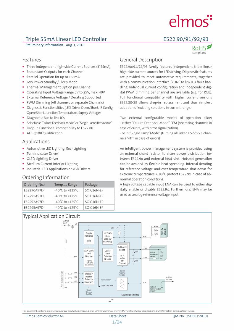
Typical Application Circuit
Three independent high-side Current Sources (3*55mA)
Redundant Outputs for each Channel
Parallel Operation for up to 165mA
Low Power Standby / Sleep Mode
Thermal Management Option per Channel
Operating Input Voltage Range 5V to 25V, max. 40V
External Reference Voltage / Derating Supported
PWM Dimming (All channels or separate Channels)
Diagnostic Functionalities (LED Driver Open/Short, IR Config
Open/Short, Junction Temperature, Supply Voltage)
Diagnostic Bus to link ICs
Selectable “Failure Feedback Mode” or “Single Lamp Behaviour”
Drop-In Functional compatibility to E522.80
AEC-Q100 Qualification
Automotive LED Lighting, Rear Lighting
Turn Indicator Driver
OLED Lighting Driver
Medium Current Interior Lighting
Industrial LED Applications or RGB Drivers
General DescriptionE522.90/91/92/93 family features independent triple linear
high-side current sources for LED driving. Diagnostic features
are provided to meet automotive requirements, together
with a communication interface “RUN” to link ICs fault han-
dling. Individual current configuration and independent dig-
ital PWM dimming per channel are available (e.g. for RGB).
Full functional compatibility with higher current versions
E522.80-83 allows drop-in replacement and thus simplest
adaption of existing solutions in current range.
Two external configurable modes of operation allow
- either “Failure Feedback Mode” FFM (operating channels in
case of errors, with error signalization)
- or in “Single Lamp Mode” (turning all linked E522.9x s chan-
nels “off” in case of errors)
An intelligent power management system is provided using
an external shunt resistor to share power distribution be-
tween E522.9x and external heat sink. Hotspot generation
can be avoided by flexible heat spreading. Internal derating
for reference voltage and over-temperature shut-down for
extreme temperatures >180°C protect E522.9x in case of ab-
normal operation conditions.
A high voltage capable input ENA can be used to either dig-
itally enable or disable E522.9x. Furthermore, ENA may be
used as analog reference voltage input.
Ordering InformationOrdering-No.: TempAmb Range Package
E52290A97D -40°C to +125°C SOIC16N-EP
E52291A97D -40°C to +125°C SOIC16N-EP
E52292A97D -40°C to +125°C SOIC16N-EP
E52293A97D -40°C to +125°C SOIC16N-EP
LEDxA
RUN
RUNx
RUNy
RUNz
LEDxB
SLM
GND
IR 1
VS
IR 2
IR 3
From
Con
trolle
r / to
GND
E522.90/91/92/93
SupplyReference
OVT
HV DIAGOpen
Drain I/Owith Pullup
E522
.9xE5
22.8x
Open /Short
Detection@ LEDx
Error Detection
CurrentReferencefor LEDx
ENA
OFF
CurrentReferencefor LEDx
Single Lamp Mode
ENA Dimmand
Derating
- High VS- High Temp
- Ext. Derating
Disable /ResistorDriver for
External R
OFF
ThermalManagementResistor
OptionalFailure FeedbackCircuitry
to BCM /Controller
SwitchedSupply
3x CurrentSource
up to55mAper
Channel
ENA
2/24
Triple 55mA Linear LED Controller E522.90/91/92/93Preliminary Information - Aug 3, 2016
Elmos Semiconductor AG Data Sheet QM-No.: 25DS0159E.01
This document contains information on a pre-production product. Elmos Semiconductor AG reserves the right to change specifications and information herein without notice.
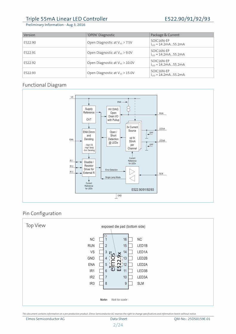
Functional Diagram
Pin Configuration
Top View
Note: Not to scale
LEDxA
RUN
RUNx
RUNy
RUNz
LEDxB
SLM
GND
IR 1
VS
IR 2
IR 3
From
Con
trolle
r / to
GND
E522.90/91/92/93
SupplyReference
OVT
HV DIAGOpen
Drain I/Owith Pullup
E522
.9xE5
22.8x
Open /Short
Detection@ LEDx
Error Detection
CurrentReferencefor LEDx
ENA
OFF
CurrentReferencefor LEDx
Single Lamp Mode
ENA Dimmand
Derating
- High VS- High Temp
- Ext. Derating
Disable /ResistorDriver for
External R
OFF
ThermalManagementResistor
OptionalFailure FeedbackCircuitry
to BCM /Controller
SwitchedSupply
3x CurrentSource
up to55mAper
Channel
ENA
Version ‘OPEN’ Diagnostic Package & Current
E522.90 Open Diagnostic at VVS > 7.5V SOIC16N-EPILED = 14.2mA...55.2mA
E522.91 Open Diagnostic at VVS > 9.0V SOIC16N-EPILED = 14.2mA...55.2mA
E522.92 Open Diagnostic at VVS > 10.0V SOIC16N-EPILED = 14.2mA...55.2mA
E522.93 Open Diagnostic at VVS > 15.0V SOIC16N-EPILED = 14.2mA...55.2mA
1 16NC NC2 15RUN LED1B3 14VS LED1A4 13GND LED2B5 12ENA LED2A6 11IR1 LED3B7 10IR2 LED3A8 9IR3 SLM
exposed die pad (bottom side)
E522
.9x
3/24
Triple 55mA Linear LED Controller E522.90/91/92/93Preliminary Information - Aug 3, 2016
Elmos Semiconductor AG Data Sheet QM-No.: 25DS0159E.01
This document contains information on a pre-production product. Elmos Semiconductor AG reserves the right to change specifications and information herein without notice.
Pin Description
Pin Name Type 1) Description1 NC A_I Not connected internally2 RUN HV_A_IO RUN Diagnostic Bus Interface to link E522.9x or E522.8x Products3 VS HV_S High-Voltage Supply Input4 GND S Ground Connection5 ENA HV_A_I High-Voltage Enable and optional analog Referencevoltage Input6 IR1 A_IO Current Configuration Channel 1, digital Input for Channel 1 dimming7 IR2 A_IO Current Configuration Channel 2, digital Input for Channel 2 dimming8 IR3 A_IO Current Configuration Channel 3, digital Input for Channel 3 dimming9 SLM A_IO Operating Mode Configuration (“Single Lamp Mode” or “Failure Feedback” Operation)10 LED3A HV_A_O Bypass Output Channel 3, connect to LED directly11 LED3B HV_A_O Priority Output Channel 3, connect to LED via thermal Shunt12 LED2A HV_A_O Bypass Output Channel 2, connect to LED directly13 LED2B HV_A_O Priority Output Channel 2, connect to LED via thermal Shunt14 LED1A HV_A_O Bypass Output Channel 1, connect to LED directly15 LED1B HV_A_O Priority Output Channel 1, connect to LED via thermal Shunt16 NC A_I Not connected internally
- Exposed Pad Exposed Pad, Connect to GND for thermal connection
1) A = Analog, D = Digital, S = Supply, I = Input, O = Output, B = Bidirectional, HV = High Voltage
4/24
Triple 55mA Linear LED Controller E522.90/91/92/93Preliminary Information - Aug 3, 2016
Elmos Semiconductor AG Data Sheet QM-No.: 25DS0159E.01
This document contains information on a pre-production product. Elmos Semiconductor AG reserves the right to change specifications and information herein without notice.
1 Absolute Maximum RatingsStresses beyond these absolute maximum ratings listed below may cause permanent damage to the device. These are stress ratings only; opera-
tion of the device at these or any other conditions beyond those listed in the operational sections of this document is not implied. Exposure to
absolute maximum rated conditions for extended periods may affect device reliability. All voltages referred to VGND. Currents flowing into ter-
minals are positive, those drawn out of a terminal are negative.
No. Description Condition Symbol Min Max Unit
1 VS Pin Voltage VVS -0.3 40 V
2 ENA Pin Voltage VENA -0.3 40 V
3 IR1,2,3 Pin Voltage 1) VIR,x -0.3 5.5 V
4 IR1,2,3 Pin Current IIR,x -1 1 mA
5 LEDx Current ILED.x -70 100 mA
6 LEDxA/B Pin Voltage VLED,x -1 VVS V
7 RUN Pin Voltage VRUN -0.3 VVS V
8 RUN Pin Current IRUN -5 5 mA
9 SLM Pin Voltage VSLM -0.3 6.5 V
10 Junction Temperature Continuous TJ -40 150 °C
11 Ambient Temperature Info Parameter 2) TA -40 125 °C
12 Storage Temperature Unsoldered Device TST -40 125 °C
13 Power Dissipation tLIFETIME < 1h PV,MAX 2.5 W
14 Thermal Resistance Junction to Exposed Die Pad 3) RTH,J-C 6 K/W
No. Description Condition Symbol Min Max Unit
1 ESD HBM Protection at all Pins 1) VESD,HBM -2 2 kV
2 ESD CDM Protection at Corner Pins 2) VESD,CDM,1 -750 750 V
3 ESD CDM Protection at all other Pins 2) VESD,CDM,2 -500 500 V
1) see parameter VIR, CLMP for clamping behaviour
2) consider maximum junction temperature and cooling measures to define ambient operating range
3) Typical thermal resistance to EP is RTH,J-C = 3K/W (not production tested)
1) According to AEC-Q 100-002, Human Body Model, 1.5kΩ resistance, 100pF capacitance.
2) According to AEC-Q 100-011, Charged Device Model, pulse rise time (10% to 90%) <400ps, 1Ω resistance.
2 ESD
5/24
Triple 55mA Linear LED Controller E522.90/91/92/93Preliminary Information - Aug 3, 2016
Elmos Semiconductor AG Data Sheet QM-No.: 25DS0159E.01
This document contains information on a pre-production product. Elmos Semiconductor AG reserves the right to change specifications and information herein without notice.
No. Description Condition Symbol Min Typ Max Unit
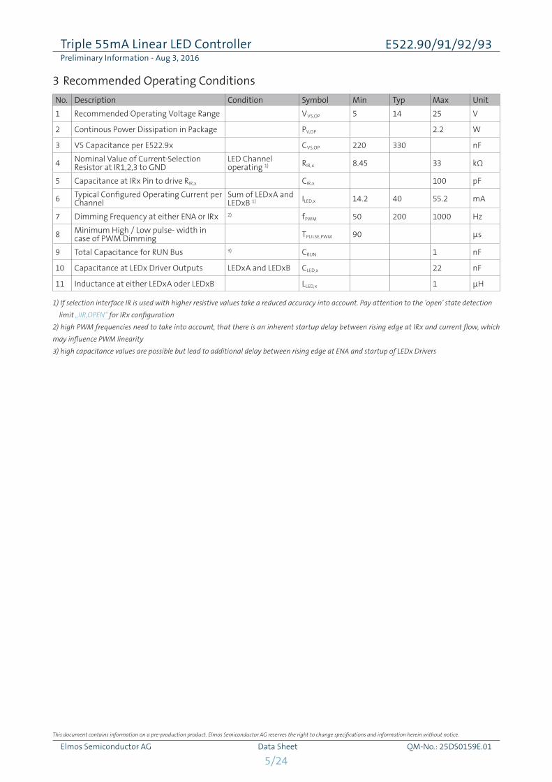
1 Recommended Operating Voltage Range VVS,OP 5 14 25 V
2 Continous Power Dissipation in Package PV,OP 2.2 W
3 VS Capacitance per E522.9x CVS,OP 220 330 nF
4 Nominal Value of Current-Selection Resistor at IR1,2,3 to GND
LED Channel operating 1) RIR,x 8.45 33 kΩ
5 Capacitance at IRx Pin to drive RIR,x CIR,x 100 pF
6 Typical Configured Operating Current per Channel
Sum of LEDxA and LEDxB 1) ILED,x 14.2 40 55.2 mA
7 Dimming Frequency at either ENA or IRx 2) fPWM 50 200 1000 Hz
8 Minimum High / Low pulse- width in case of PWM Dimming TPULSE,PWM 90 µs
9 Total Capacitance for RUN Bus 3) CRUN 1 nF
10 Capacitance at LEDx Driver Outputs LEDxA and LEDxB CLED,x 22 nF
11 Inductance at either LEDxA oder LEDxB LLED,x 1 µH
3 Recommended Operating Conditions
1) If selection interface IR is used with higher resistive values take a reduced accuracy into account. Pay attention to the ‘open’ state detection
limit „IIR,OPEN“ for IRx configuration
2) high PWM frequencies need to take into account, that there is an inherent startup delay between rising edge at IRx and current flow, which
may influence PWM linearity
3) high capacitance values are possible but lead to additional delay between rising edge at ENA and startup of LEDx Drivers
6/24
Triple 55mA Linear LED Controller E522.90/91/92/93Preliminary Information - Aug 3, 2016
Elmos Semiconductor AG Data Sheet QM-No.: 25DS0159E.01
This document contains information on a pre-production product. Elmos Semiconductor AG reserves the right to change specifications and information herein without notice.
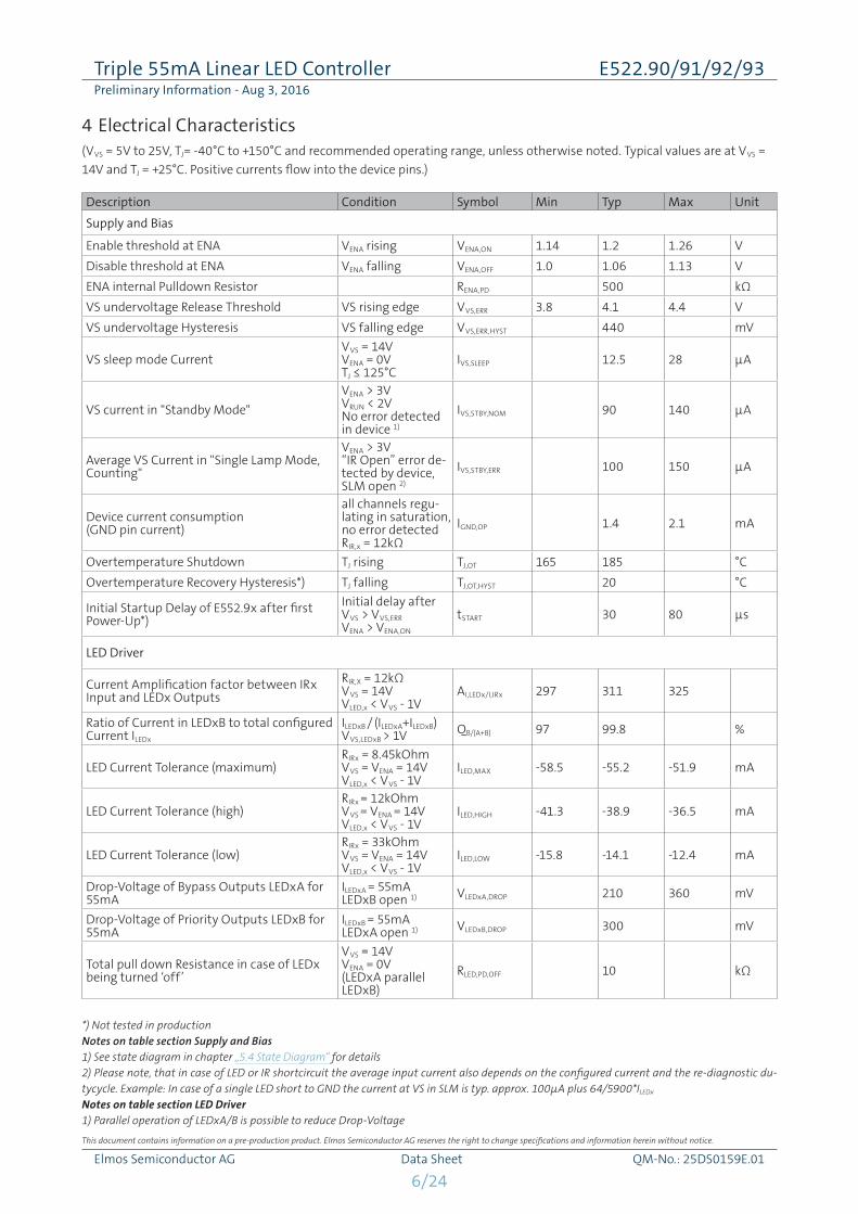
4 Electrical Characteristics(VVS = 5V to 25V, TJ= -40°C to +150°C and recommended operating range, unless otherwise noted. Typical values are at VVS =
14V and TJ = +25°C. Positive currents flow into the device pins.)
Description Condition Symbol Min Typ Max Unit
Supply and Bias
Enable threshold at ENA VENA rising VENA,ON 1.14 1.2 1.26 V
Disable threshold at ENA VENA falling VENA,OFF 1.0 1.06 1.13 V
ENA internal Pulldown Resistor RENA,PD 500 kΩ
VS undervoltage Release Threshold VS rising edge VVS,ERR 3.8 4.1 4.4 V
VS undervoltage Hysteresis VS falling edge VVS,ERR,HYST 440 mV
VS sleep mode CurrentVVS = 14VVENA = 0VTJ ≤ 125°C
IVS,SLEEP 12.5 28 µA
VS current in "Standby Mode"
VENA > 3VVRUN < 2VNo error detected in device 1)
IVS,STBY,NOM 90 140 µA
Average VS Current in "Single Lamp Mode, Counting"
VENA > 3V“IR Open” error de-tected by device,SLM open 2)
IVS,STBY,ERR 100 150 µA
Device current consumption (GND pin current)
all channels regu-lating in saturation,no error detectedRIR,x = 12kΩ
IGND,OP 1.4 2.1 mA
Overtemperature Shutdown TJ rising TJ,OT 165 185 °C
Overtemperature Recovery Hysteresis*) TJ falling TJ,OT,HYST 20 °C
Initial Startup Delay of E552.9x after first Power-Up*)
Initial delay after VVS > VVS,ERR
VENA > VENA,ON
tSTART 30 80 µs
LED Driver
Current Amplification factor between IRx Input and LEDx Outputs
RIR,X = 12kΩVVS = 14VVLED,x < VVS - 1V
AI,LEDx/I,IRx 297 311 325
Ratio of Current in LEDxB to total configured Current ILEDx
ILEDxB / (ILEDxA+ILEDxB)VVS,LEDxB > 1V QB/(A+B) 97 99.8 %
LED Current Tolerance (maximum)RIRx = 8.45kOhmVVS = VENA = 14VVLED,x < VVS - 1V
ILED,MAX -58.5 -55.2 -51.9 mA
LED Current Tolerance (high)RIRx = 12kOhmVVS = VENA = 14VVLED,x < VVS - 1V
ILED,HIGH -41.3 -38.9 -36.5 mA
LED Current Tolerance (low)RIRx = 33kOhmVVS = VENA = 14VVLED,x < VVS - 1V
ILED,LOW -15.8 -14.1 -12.4 mA
Drop-Voltage of Bypass Outputs LEDxA for 55mA
ILEDxA = 55mALEDxB open 1) VLEDxA,DROP 210 360 mV
Drop-Voltage of Priority Outputs LEDxB for 55mA
ILEDxB = 55mALEDxA open 1) VLEDxB,DROP 300 mV
Total pull down Resistance in case of LEDx being turned ‘off’
VVS = 14VVENA = 0V(LEDxA parallel LEDxB)
RLED,PD,OFF 10 kΩ
*) Not tested in productionNotes on table section Supply and Bias1) See state diagram in chapter „5.4 State Diagram“ for details2) Please note, that in case of LED or IR shortcircuit the average input current also depends on the configured current and the re-diagnostic du-tycycle. Example: In case of a single LED short to GND the current at VS in SLM is typ. approx. 100µA plus 64/5900*ILEDx
Notes on table section LED Driver1) Parallel operation of LEDxA/B is possible to reduce Drop-Voltage
7/24
Triple 55mA Linear LED Controller E522.90/91/92/93Preliminary Information - Aug 3, 2016
Elmos Semiconductor AG Data Sheet QM-No.: 25DS0159E.01
This document contains information on a pre-production product. Elmos Semiconductor AG reserves the right to change specifications and information herein without notice.
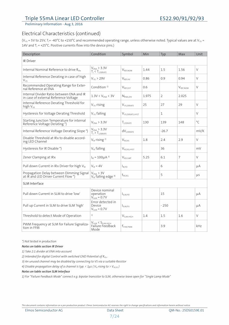
(VVS = 5V to 25V, TJ= -40°C to +150°C and recommended operating range, unless otherwise noted. Typical values are at VVS =
14V and TJ = +25°C. Positive currents flow into the device pins.)
Description Condition Symbol Min Typ Max Unit
IR Driver
Internal Nominal Reference to drive RIRxVENA > 3.3VTJ < TJ,DERATE
VREF,NOM 1.44 1.5 1.56 V
Internal Reference Derating in case of high VVS
VVS > 29V VREF,HV 0.86 0.9 0.94 V
Recommended Operating Range for Exter-nal Reference at ENA Condition 1) VREF,EXT 0.6 VREF,NOM V
Internal Divider Ratio between ENA and IR in case of external Reference Voltage 1.3V < VENA < 3V NENA,DIV 1.975 2 2.025
Internal Reference Derating Threshold for high VVS
VVS rising VVS,DERATE 25 27 29 V
Hysteresis for Voltage Derating Threshold VVS falling VVS,DERATE,HYST 1 V
Starting Junction Temperature for internal Reference Voltage Derating *) VENA > 3.3V TJ,DERATE 130 139 148 °C
Internal Reference Voltage Derating Slope *) VENA > 3.3VTJ > TJ,DERATE
dVJ,DERATE -26.7 mV/K
Disable Threshold at IRx to disable accord-ing LED Channel VIR rising 2) VIR,DIS 1.8 2.4 2.9 V
Hysteresis for IR Disable *) VIR falling VIR,DIS,HYST 36 mV
Zener Clamping at IRx IIR = 100µA 3) VIR,CLMP 5.25 6.1 7 V
Pull down Current in IRx Driver for high VIR VIR = 4V IIR,PD 6 µA
Propagation Delay between Dimming Signalat IR and LED Driver Current Flow *)
VENA > 3VVIR falling edge 4) tIR,DEL 5 µs
SLM Interface
Pull down Current in SLM to drive 'low'Device nominal operationVSLM = 0.7V
ISLM,PD 15 µA
Pull up Current in SLM to drive SLM 'high'Error detected in DeviceVSLM = 0.7V
ISLM,PU - 250 µA
Threshold to detect Mode of Operation 1) VSLM,HIGH 1.4 1.5 1.6 V
PWM Frequency at SLM for Failure Signaliza-tion in FFM
VSLM < SSLM,HIGH
Failure Feedback Mode
fFFM,PWM 3.9 kHz
Electrical Characteristics (continued)
*) Not tested in production
Notes on table section IR Driver
1) Take 2:1 divider at ENA into account
2) Intended for digital Control with switched GND Potential of RIR,x
3) An unused channel may be disabled by connecting to VS via a suitable Resistor
4) Disable propagation delay of a channel is typ. < 1µs ( VIR rising to > VIR,DIS )
Notes on table section SLM Interface
1) For “Failure Feedback Mode” connect e.g. bipolar transistor to SLM, otherwise leave open for “Single Lamp Mode”
8/24
Triple 55mA Linear LED Controller E522.90/91/92/93Preliminary Information - Aug 3, 2016
Elmos Semiconductor AG Data Sheet QM-No.: 25DS0159E.01
This document contains information on a pre-production product. Elmos Semiconductor AG reserves the right to change specifications and information herein without notice.
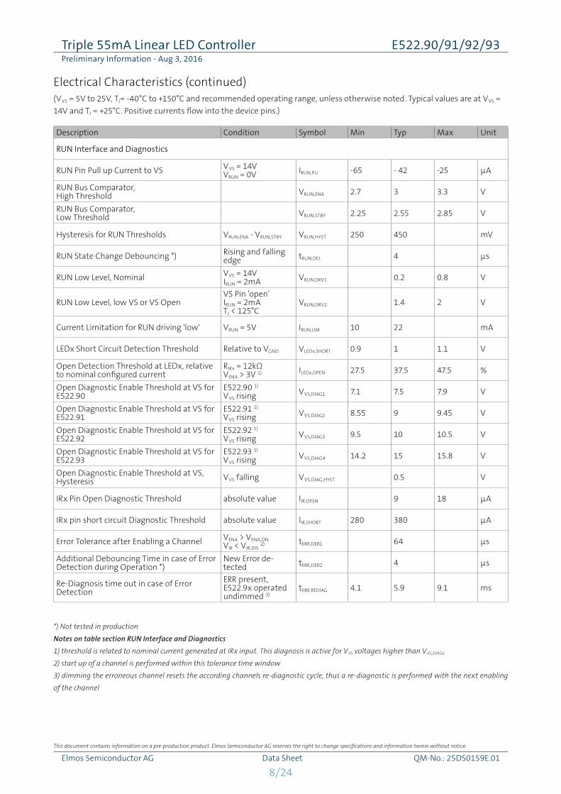
Description Condition Symbol Min Typ Max Unit
RUN Interface and Diagnostics
RUN Pin Pull up Current to VS VVS = 14VVRUN = 0V IRUN,PU -65 - 42 -25 µA
RUN Bus Comparator,High Threshold VRUN,ENA 2.7 3 3.3 V
RUN Bus Comparator,Low Threshold VRUN,STBY 2.25 2.55 2.85 V
Hysteresis for RUN Thresholds VRUN,ENA - VRUN,STBY VRUN,HYST 250 450 mV
RUN State Change Debouncing *) Rising and falling edge tRUN,DEL 4 µs
RUN Low Level, Nominal VVS = 14VIRUN = 2mA VRUN,DRV1 0.2 0.8 V
RUN Low Level, low VS or VS OpenVS Pin ‘open’IRUN = 2mATJ < 125°C
VRUN,DRV2 1.4 2 V
Current Limitation for RUN driving 'low' VRUN = 5V IRUN,LIM 10 22 mA
LEDx Short Circuit Detection Threshold Relative to VGND VLEDx,SHORT 0.9 1 1.1 V
Open Detection Threshold at LEDx, relative to nominal configured current
RIRx = 12kΩVENA > 3V 1) ILEDx,OPEN 27.5 37.5 47.5 %
Open Diagnostic Enable Threshold at VS for E522.90
E522.90 1)
VVS rising VVS,DIAG1 7.1 7.5 7.9 V
Open Diagnostic Enable Threshold at VS for E522.91
E522.91 1)
VVS rising VVS,DIAG2 8.55 9 9.45 V
Open Diagnostic Enable Threshold at VS for E522.92
E522.92 1)
VVS rising VVS,DIAG3 9.5 10 10.5 V
Open Diagnostic Enable Threshold at VS for E522.93
E522.93 1)
VVS rising VVS,DIAG4 14.2 15 15.8 V
Open Diagnostic Enable Threshold at VS, Hysteresis VVS falling VVS,DIAG,HYST 0.5 V
IRx Pin Open Diagnostic Threshold absolute value IIR,OPEN 9 18 µA
IRx pin short circuit Diagnostic Threshold absolute value IIR,SHORT 280 380 µA
Error Tolerance after Enabling a Channel VENA > VENA,ON
VIR < VIR,DIS 2) tERR,DEB1 64 µs
Additional Debouncing Time in case of Error Detection during Operation *)
New Error de-tected tERR,DEB2 4 µs
Re-Diagnosis time out in case of Error Detection
ERR present, E522.9x operated undimmed 3)
tERR,REDIAG 4.1 5.9 9.1 ms
*) Not tested in production
Notes on table section RUN Interface and Diagnostics
1) threshold is related to nominal current generated at IRx input. This diagnosis is active for VVS voltages higher than VVS,DIAGx
2) start up of a channel is performed within this tolerance time window
3) dimming the erroneous channel resets the according channels re-diagnostic cycle, thus a re-diagnostic is performed with the next enabling
of the channel
(VVS = 5V to 25V, TJ= -40°C to +150°C and recommended operating range, unless otherwise noted. Typical values are at VVS =
14V and TJ = +25°C. Positive currents flow into the device pins.)
Electrical Characteristics (continued)
9/24
Triple 55mA Linear LED Controller E522.90/91/92/93Preliminary Information - Aug 3, 2016
Elmos Semiconductor AG Data Sheet QM-No.: 25DS0159E.01
This document contains information on a pre-production product. Elmos Semiconductor AG reserves the right to change specifications and information herein without notice.
E522.90/91/92/93 family devices provide independent triple linear current controller for LED driving, which can optionally be
operated in parallel for higher current requirements. These family members support individual current configuration and in-
dependent digital PWM dimming per channel (see IR interface).
Various diagnostic features are provided to meet automotive requirements, together with a communication interface named
“RUN” to link ICs to generate more than three channels. ICs linked in this way can be operated as a combined cluster of drivers,
turning ‘on’ and ‘off’ in parallel (e.g. turning all drivers ‘off’ in case of hardware failures).
Two external configurable modes of operation allow
- either “Failure Feedback Mode” FFM (operating channels in case of errors, with error signalization)
- or in “Single Lamp Mode” (turning all linked E522.9x/E522.8x s channels “off” in case of errors)
Typical exemplary application topologies are presented in „5.7 Exemplary Application Topologies“.
More information on the LEDx drivers and power management can be found in „5.2 LED Driver“.
For more details on the configuration and dimming via IRx interface see „5.3 IR Driver“.
A detailed overview of functional states is given in „5.4 State Diagram“.
Configuration of FFM or Single Lamp Mode is described in „5.5 SLM Interface“.
Diagnostic features are located in „5.6 RUN Interface and Diagnostics“.
Dimensioning formulars can be found in „5.8 Dimensioning Formulas and Power Calculation“
Device Family members for more simple implementations are provided with E522.84-87, featuring a high degree of functional
compatibility to E522.90-93 at e.g. “RUN” pin. For higher output currents at full functional compatibility with E522.9x there are
E522.80-83 available. Please refer to the according datasheets for more details on those products.
High-side drivers for LEDX provide the current configured by the according IRX pin, reproducing the IIRx with a typical amplifi-
cation factor of 311:1. In E522.90-93 there are two outputs LEDxA and LEDxB per channel. The outputs can either be used for
redundancy (in parallel) or for advanced thermal management to share the IC power with external power sinks as follows (see
Typical Application Diagram):
5 Functional Description5.1 Overview
5.2 LED Driver
5 8 11 14 17 20 23 26 29 320
0,1
0,2
0,3
0,4
0,5
0,6
0,7
0,8
0,9
1
Power Distribution Principle in E522.90/91/92/93 Applications
Power as a function of V ( VS )Exemplary for V ( LED ) = 6V and different ext. Shunts
( Single-Channel Calculation for 55mA )
P (LED)P (R1 = 62 Ohm)P (E522.9x) @ R1P (R2 = 120 Ohm)P (E522.9x) @ R2P (R3 = 180 Ohm)P (E522.9x) @ R3
V (VS) [ V ]
P [
W ]
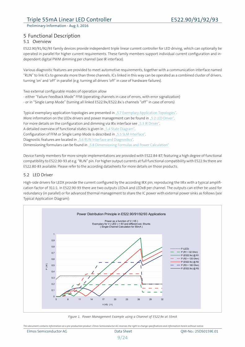
Figure 1. Power Management Example using a Channel of E522.9x at 55mA
10/24
Triple 55mA Linear LED Controller E522.90/91/92/93Preliminary Information - Aug 3, 2016
Elmos Semiconductor AG Data Sheet QM-No.: 25DS0159E.01
This document contains information on a pre-production product. Elmos Semiconductor AG reserves the right to change specifications and information herein without notice.
To handle the power that is generated in linear LED drivers, the E522.90-93 device family offers an advanced power distribu-
tion feature. The channels current is regulated as a sum of currents in LEDxA and LEDxB. The priority output LEDxB drives the
current as long as the voltage headroom allows to. If current in LEDxB drops below the target value, the bypass output LEDxA
is automatically activated to deliver the remaining current.
This distribution of current allows to share some of the linear regulator power with the external Power-Shunt. „Figure 1. Power
Management Example using a Channel of E522.9x at 55mA“ shows the basic power generation per channel in (as a function
of VVS)
- the LED load driven
- in the external power shunt, given for exemplary values R1=68Ω, R2=120Ω, R3=180Ω
- plus the remaining power for one channel in E522.9x
For calculations, this principle offers two points of virtually “zero” power in E522.9x, one for the VVS,Z1 = VLED and a second “zero”
power point at VVS,Z2 = VLED + ILED * RPOWERSHUNT. Beyond VVS,Z2 the power in E522.9x starts to increase linearly as for common linear
LED drivers. For E522.9x the local power maximum between VVS,Z1 and VVS,Z2 is always 0.25 * RPOWERSHUNT * ILED2 .
At the voltage derating threshold VVS,DERATE the internal reference is reduced to 60% of nominal, thus the overall system power
is reduced as shown to avoid excessive heat generation in case of e.g. load dump pulses.
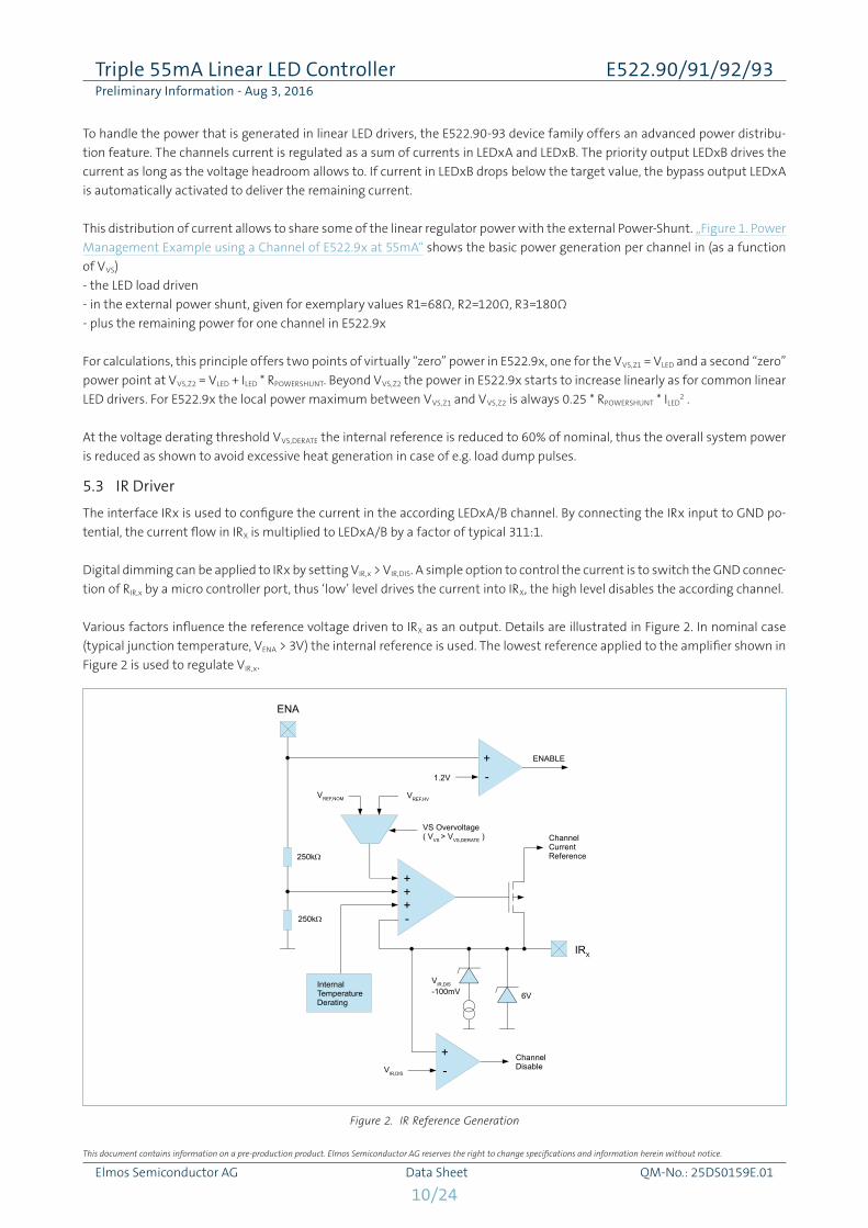
The interface IRx is used to configure the current in the according LEDxA/B channel. By connecting the IRx input to GND po-
tential, the current flow in IRX is multiplied to LEDxA/B by a factor of typical 311:1.
Digital dimming can be applied to IRx by setting VIR,x > VIR,DIS. A simple option to control the current is to switch the GND connec-
tion of RIR,x by a micro controller port, thus ‘low’ level drives the current into IRX, the high level disables the according channel.
Various factors influence the reference voltage driven to IRX as an output. Details are illustrated in Figure 2. In nominal case
(typical junction temperature, VENA > 3V) the internal reference is used. The lowest reference applied to the amplifier shown in
Figure 2 is used to regulate VIR,x.
5.3 IR Driver
+++-
+-1.2V
ENABLE
VREF,NOM
250kΩ
250kΩ
InternalTemperatureDerating
VREF,HV
VS Overvoltage( VVS > VVS,DERATE )
ENA
ChannelCurrent Reference
+-VIR,DIS
ChannelDisable
IRX
VIR,DIS
-100mV 6V
Figure 2. IR Reference Generation
11/24
Triple 55mA Linear LED Controller E522.90/91/92/93Preliminary Information - Aug 3, 2016
Elmos Semiconductor AG Data Sheet QM-No.: 25DS0159E.01
This document contains information on a pre-production product. Elmos Semiconductor AG reserves the right to change specifications and information herein without notice.
In case that less than three current drivers are needed, the internal clamping as shown in „Figure 2. IR Reference Generation“
allows to connect this input to e.g. VS directly by a resistor of typ. 100kΩ.
Note that this resistor will contribute to the overall sleep mode or standby current of the application.
Connecting the IRX inputs statically to other supply voltages VSUPPLY > VIR,DIS is also possible to effectively disable the according
channel. Please note, that the maximum supply voltage to turn IRX ‘off’ may be restricted by the clamping voltage at this pin,
see parameter „VIR,CLMP“.
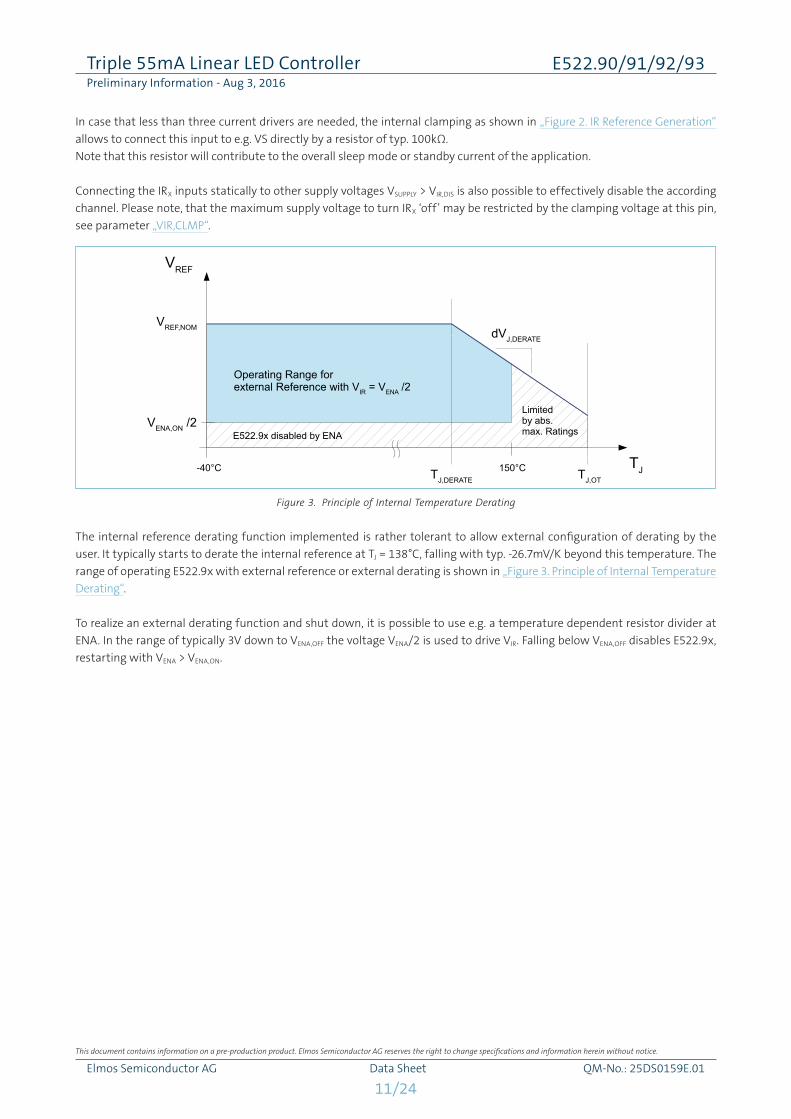
The internal reference derating function implemented is rather tolerant to allow external configuration of derating by the
user. It typically starts to derate the internal reference at TJ = 138°C, falling with typ. -26.7mV/K beyond this temperature. The
range of operating E522.9x with external reference or external derating is shown in „Figure 3. Principle of Internal Temperature
Derating“.
To realize an external derating function and shut down, it is possible to use e.g. a temperature dependent resistor divider at
ENA. In the range of typically 3V down to VENA,OFF the voltage VENA/2 is used to drive VIR. Falling below VENA,OFF disables E522.9x,
restarting with VENA > VENA,ON.
TJ
VREF
TJ,DERATE
dVJ,DERATE
TJ,OT
Operating Range forexternal Reference with VIR = VENA /2
VREF,NOM
VENA,ON /2
150°C-40°C
E522.9x disabled by ENA
Limitedby abs.max. Ratings
Figure 3. Principle of Internal Temperature Derating
12/24
Triple 55mA Linear LED Controller E522.90/91/92/93Preliminary Information - Aug 3, 2016
Elmos Semiconductor AG Data Sheet QM-No.: 25DS0159E.01
This document contains information on a pre-production product. Elmos Semiconductor AG reserves the right to change specifications and information herein without notice.
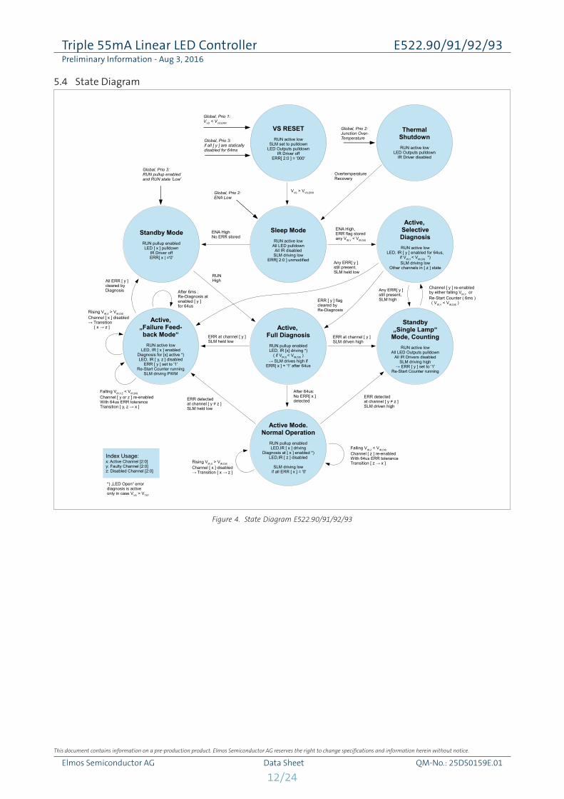
5.4 State Diagram
Active, Full Diagnosis
RUN pullup enabledLED, IR [x] driving *)
( if VIR,X < VIR,DIS )→ SLM drives high if
ERR[ x ] = '1' after 64us
Sleep ModeRUN active low
All LED pulldownAll IR disabled
SLM driving lowERR[ 2:0 ] unmodified
VVS > VVS,ERR
Active,„Failure Feed-back Mode“
RUN active lowLED, IR [ x ] enabled
Diagnosis for [x] active *)LED, IR [ y, z ] disabled
ERR [ y ] set to '1'Re-Start Counter running
SLM driving PWM
Standby„Single Lamp“
Mode, CountingRUN active low
All LED Outputs pulldownAll IR Drivers disabled
SLM driving high→ ERR [ y ] set to '1'
Re-Start Counter running
ERR at channel [ y ]SLM driven high
ERR at channel [ y ]SLM held low
Active, SelectiveDiagnosisRUN active low
LED, IR [ y ] enabled for 64us,if VIR,Y < VIR,DIS *)SLM driving low
Other channels in [ z ] state
ENA High,ERR flag storedany VIR,Y < VIR,DIS
Standby ModeRUN pullup enabledLED [ x ] pulldown
IR Driver offERR[ x | ='0'
RUNHigh
Channel [ y ] re-enabledby either falling VIR,Y orRe-Start Counter ( 6ms ) ( VIR,Y < VIR,DIS )
Global, Prio 1:VVS < VVS,ERR
Active Mode.Normal Operation
RUN pullup enabledLED,IR [ x ] driving
Diagnosis at [ x ] enabled *)LED,IR [ z ] disabled
SLM driving low if all ERR [ x ] = '0'
After 64us:No ERR[ x ]detected
ERR detectedat channel [ y ≠ z ]SLM driven high
ERR detectedat channel [ y ≠ z ]SLM held low
Global, Prio 3:RUN pullup enabledand RUN state 'Low'
Any ERR[ y ] still present,SLM highERR [ y ] flag
cleared byRe-Diagnosis
ThermalShutdownRUN active low
LED Outputs pulldownIR Driver disabled
Global, Prio 2:Junction Over-Temperature
*) „LED Open“ errordiagnosis is activeonly in case VVS > VTST
ENA HighNo ERR stored
OvertemperatureRecovery
Global, Prio 2:ENA Low
Any ERR[ y ]still present,SLM held low
Rising VIR,X > VIR,DIS
Channel [ x ] disabled→ Transition [ x → z ]
Falling VIR,Y,Z < VIR,DIS
Channel [ y or z ] re-enabledWith 64us ERR tolerance Transition [ y, z → x ]
Index Usage:x: Active Channel [2:0]y: Faulty Channel [2:0]z: Disabled Channel [2:0]
After 6ms :Re-Diagnosis atenabled [ y ] for 64us
Rising VIR,X > VIR,DIS
Channel [ x ] disabled→ Transition [ x → z ]
Falling VIR,Z < VIR,DIS
Channel [ z ] re-enabledWith 64us ERR tolerance Transition [ z → x ]
All ERR [ y ]cleared byDiagnosis
Global, Prio 3:if all [ y ] are staticallydisabled for 64ms
VS RESETRUN active low
SLM set to pulldownLED Outputs pulldown
IR Driver offERR[ 2:0 ] = '000'
Figure 4. State Diagram E522.90/91/92/93
13/24
Triple 55mA Linear LED Controller E522.90/91/92/93Preliminary Information - Aug 3, 2016
Elmos Semiconductor AG Data Sheet QM-No.: 25DS0159E.01
This document contains information on a pre-production product. Elmos Semiconductor AG reserves the right to change specifications and information herein without notice.
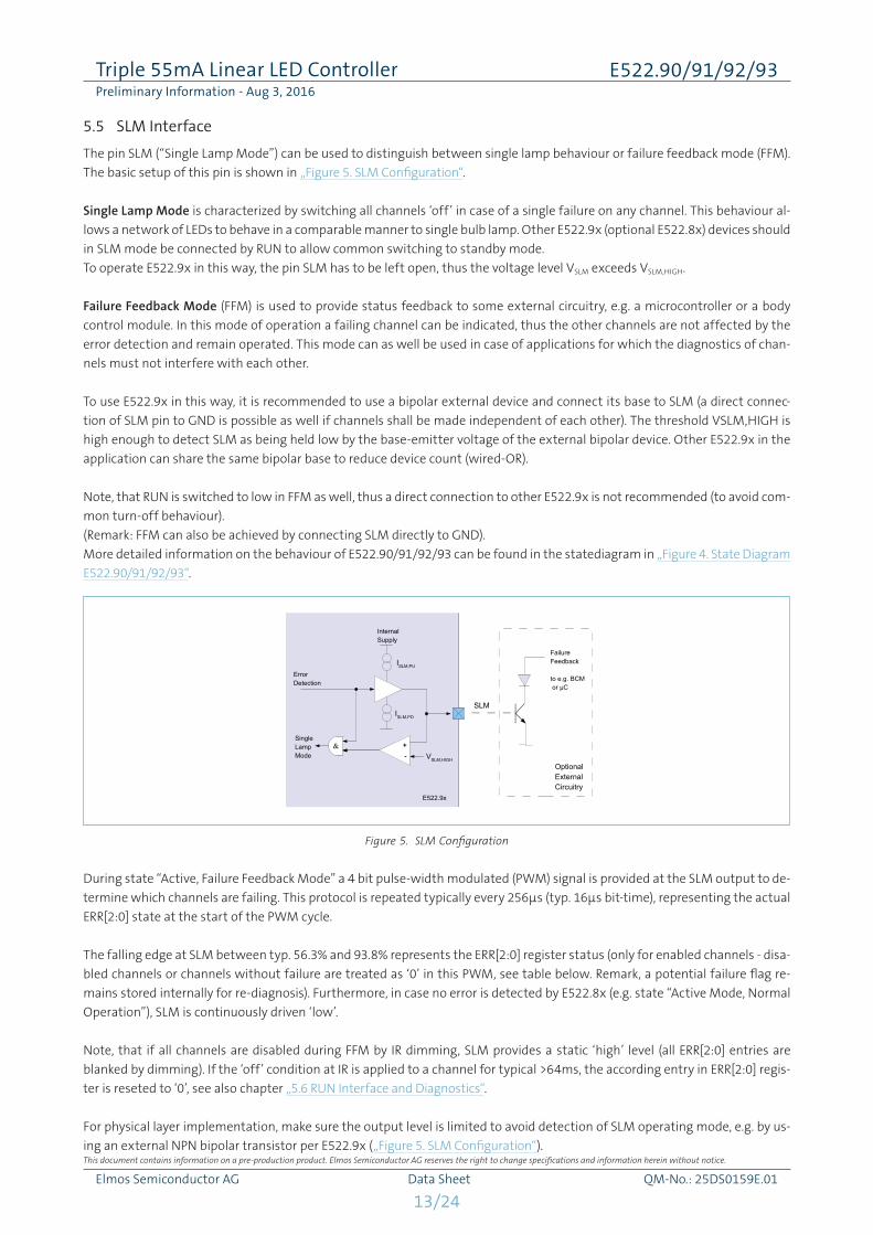
5.5 SLM Interface
The pin SLM (“Single Lamp Mode”) can be used to distinguish between single lamp behaviour or failure feedback mode (FFM).
The basic setup of this pin is shown in „Figure 5. SLM Configuration“.
Single Lamp Mode is characterized by switching all channels ‘off’ in case of a single failure on any channel. This behaviour al-
lows a network of LEDs to behave in a comparable manner to single bulb lamp. Other E522.9x (optional E522.8x) devices should
in SLM mode be connected by RUN to allow common switching to standby mode.
To operate E522.9x in this way, the pin SLM has to be left open, thus the voltage level VSLM exceeds VSLM,HIGH.
Failure Feedback Mode (FFM) is used to provide status feedback to some external circuitry, e.g. a microcontroller or a body
control module. In this mode of operation a failing channel can be indicated, thus the other channels are not affected by the
error detection and remain operated. This mode can as well be used in case of applications for which the diagnostics of chan-
nels must not interfere with each other.
To use E522.9x in this way, it is recommended to use a bipolar external device and connect its base to SLM (a direct connec-
tion of SLM pin to GND is possible as well if channels shall be made independent of each other). The threshold VSLM,HIGH is
high enough to detect SLM as being held low by the base-emitter voltage of the external bipolar device. Other E522.9x in the
application can share the same bipolar base to reduce device count (wired-OR).
Note, that RUN is switched to low in FFM as well, thus a direct connection to other E522.9x is not recommended (to avoid com-
mon turn-off behaviour).
(Remark: FFM can also be achieved by connecting SLM directly to GND).
More detailed information on the behaviour of E522.90/91/92/93 can be found in the statediagram in „Figure 4. State Diagram
E522.90/91/92/93“.
During state “Active, Failure Feedback Mode” a 4 bit pulse-width modulated (PWM) signal is provided at the SLM output to de-
termine which channels are failing. This protocol is repeated typically every 256µs (typ. 16µs bit-time), representing the actual
ERR[2:0] state at the start of the PWM cycle.
The falling edge at SLM between typ. 56.3% and 93.8% represents the ERR[2:0] register status (only for enabled channels - disa-
bled channels or channels without failure are treated as ‘0’ in this PWM, see table below. Remark, a potential failure flag re-
mains stored internally for re-diagnosis). Furthermore, in case no error is detected by E522.8x (e.g. state “Active Mode, Normal
Operation”), SLM is continuously driven ‘low’.
Note, that if all channels are disabled during FFM by IR dimming, SLM provides a static ‘high’ level (all ERR[2:0] entries are
blanked by dimming). If the ‘off’ condition at IR is applied to a channel for typical >64ms, the according entry in ERR[2:0] regis-
ter is reseted to ‘0’, see also chapter „5.6 RUN Interface and Diagnostics“.
For physical layer implementation, make sure the output level is limited to avoid detection of SLM operating mode, e.g. by us-
ing an external NPN bipolar transistor per E522.9x („Figure 5. SLM Configuration“).
InternalSupply
VSLM,HIGH
ErrorDetection
SingleLampMode
ISLM,PU
ISLM,PD
SLM
FailureFeedback
to e.g. BCM or µC
E522.9x
OptionalExternalCircuitry
+-
&
Figure 5. SLM Configuration
14/24
Triple 55mA Linear LED Controller E522.90/91/92/93Preliminary Information - Aug 3, 2016
Elmos Semiconductor AG Data Sheet QM-No.: 25DS0159E.01
This document contains information on a pre-production product. Elmos Semiconductor AG reserves the right to change specifications and information herein without notice.
PWM Dutycycle ERR[2], channel LEDx3 ERR[1], channel LEDx2 ERR[0], channel LEDx1100% '0' '0' '0'93.8% '0' '0' '1'87.5% '0' '1' '0'81.3% '0' '1' '1'75.0% '1' '0' '0'68.8% '1' '0' '1'62.5% '1' '1' '0'56.3% '1' '1' '1'
Table 1. PWM Dutycycle Reference Table for State “Active, Failure Feedback Mode”
Digital ‘0’ represents either correct operation at LEDx or disabled channels ( VIR,x > VIR,DIS )
Example A: PWM in case of channel LEDx2 failure detection (all channels enabled):
ERR[2:0] = ‘010’ ( no failures blanked by dimming at IRx )
=> PWM Dutycycle of 87.5%
Example B: PWM in case of channel LEDx2 & LEDx3 failure detection (channel LEDx2 disabled):
ERR[2:0] = ‘110’ ( failure at channel 2 is blanked by dimming, thus the relevant register value becomes ‘100’ )
=> PWM Dutycycle of 75.0%
Diagnostic features provided in E522.90-93 include the monitoring of
High resistive IRX drivers for each channel (e.g. in case of ‘open’ connection for any of the connected devices)
Short-circuit at IRX drivers to GND for each channel
Short circuit of LEDxA/B to GND for each channel (checking for a static threshold of VLEDx,SHORT)
Open LEDxA connections for each channel (E522.9x family members provide different thresholds of VVS to enable this
monitor, thus avoiding wrong ‘OPEN’ error detection in case VVS is smaller than the forward voltage of the LEDs (VLED)
Internal junction overtemperature (disabling all channels)
VVS voltage monitoring for undervoltage (providing defined behaviour for slow supply ramping)
The driver “OPEN” detection is relative to the actual current configured at IRX. This detection is active if the supply VVS is higher
than VVS,DIAGx, which is a family member specific threshold.
If a defect at any of the channels is detected, it is stored for selective re-diagnosis. Dimming at either ENA or VIR does not delete
this information. A diagnosis cycle showing removal of the erroneous conditions, VS under-voltage or permanent disable of all
failing channels via IR input (see below) resets the stored flag(s) to ‘0’.
Erroneous channels can be deactivated and removed from state consideration by setting the according VIR,y > VIR,DIS. Once the
disable request exceeds a length of typ. 64ms (in any mode other than ‘Sleep Mode’ or ‘VS Reset’), the channel will no longer
be considered for SLM or FFM state. In this way, e.g. a SLM application may be re-enabled (without the erroneous channel). For
details see statediagram, global transitions into VS_RESET state.
Re-diagnosis in case of continuous operation is performed on a regular time-basis of tERR,REDIAG to allow replacement of defect
loads / LEDs for such applications.
A loss of VS connection for a single E522.9x is propagated via RUN being set to low, as well as for ENA being ‘low’ (e.g. in case
of ‘OPEN’ failure at ENA).
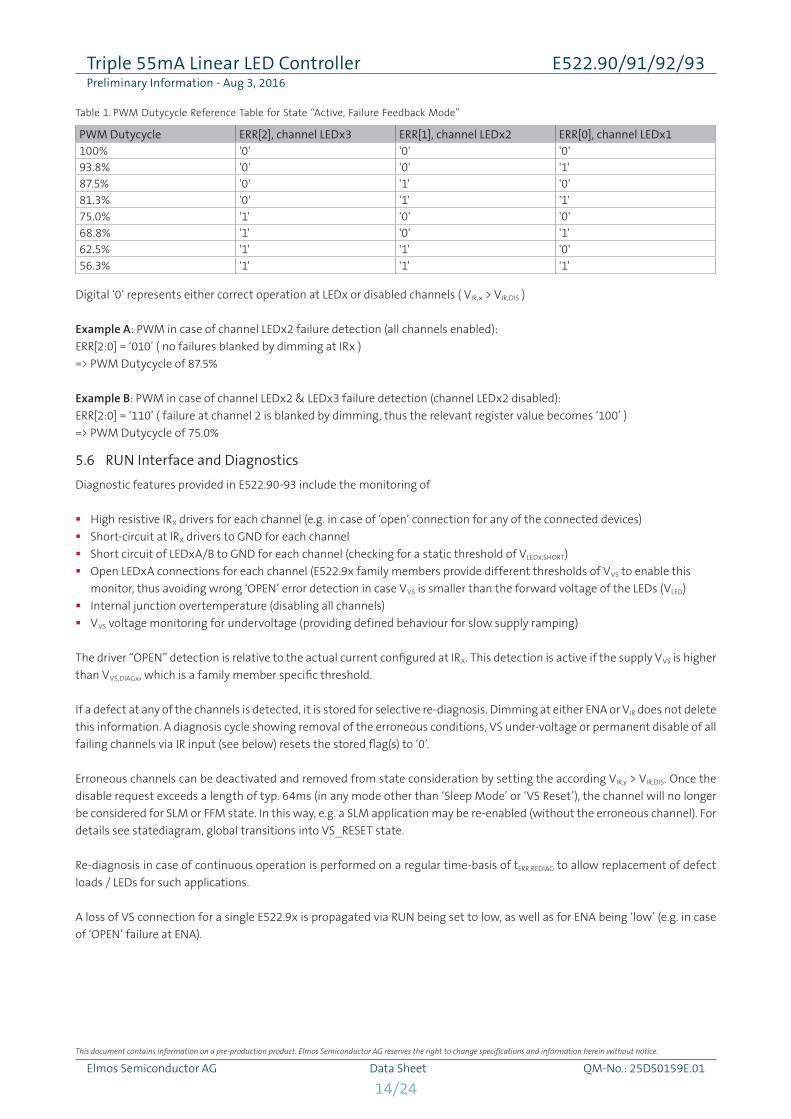
5.6 RUN Interface and Diagnostics
15/24
Triple 55mA Linear LED Controller E522.90/91/92/93Preliminary Information - Aug 3, 2016
Elmos Semiconductor AG Data Sheet QM-No.: 25DS0159E.01
This document contains information on a pre-production product. Elmos Semiconductor AG reserves the right to change specifications and information herein without notice.
The basic structure of the RUN interface is shown in Figure 6. Please note, that the purpose of the RUN bus is to form a direct
connection to other family members E522.9x or local circuitry, preferably on the same PCB. Only in this case or if RUN is unused,
the components CRUN and RRUN,PU may be omitted. They are recommended to protect the bus for additional requirements (e.g.
EMC). The interface itself is not designed for usage in a wiring harness without adequate protective measures.
The limits for usable values for CRUN and RRUN,PU are given by the tolerable delay at startup or from standby together with the cur-
rent limitation for the RUN interface (see „RUN Interface and Diagnostics“). Furthermore, RRUN,PU can contribute to sleepmode
current consumption due to RUN being driven active low in this case.
RUN
VRUN,ENA
IRUN,PU
VRUN,STBY
e.g. Sleepmodeor Fault detected
VS
VS
RRUN,PU*)
CRUN*)
to e.g. other E522.9x or E522.8x
e.g. Sleepmode
RUN Levelto Statemachine
*) see decription
E522.9x
Figure 6. RUN Interface
16/24
Triple 55mA Linear LED Controller E522.90/91/92/93Preliminary Information - Aug 3, 2016
Elmos Semiconductor AG Data Sheet QM-No.: 25DS0159E.01
This document contains information on a pre-production product. Elmos Semiconductor AG reserves the right to change specifications and information herein without notice.
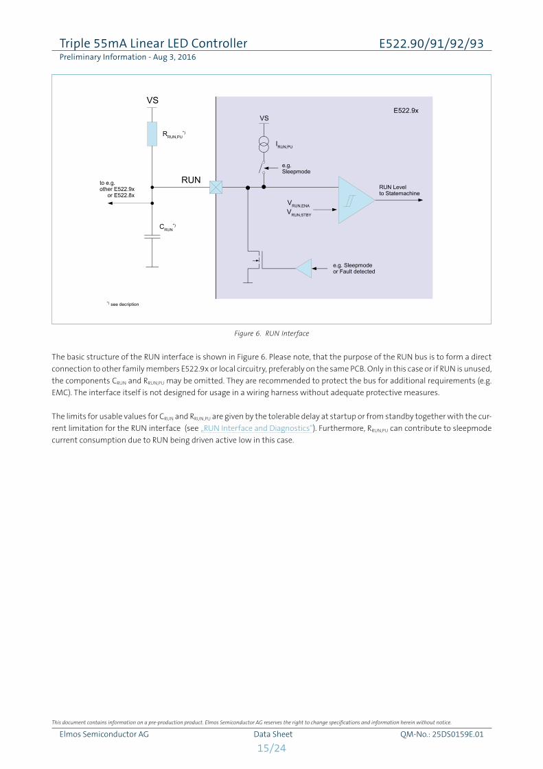
This chapter provides various exemplary Application topologies and use-cases for E522.90/91/92/93. From basic setup to full
automotive setup there are typical options given, which of course can be combined to more complex systems. Please make
sure, that examples taken from this chapter fulfil your application requirements.
This is an exemplary basic implementation using E522.90/91/92/93 Family members. The basic features are
- Permanent operation of all LED strings
- Individual current configuration for each LED String
- Channels diagnostic does not interfere between channels (FFM mode used - see SLM pin and RUN pin open)
- Capacitors at the LED loads are used to improve PSRR of the circuit or to protect LEDs from ESD pulses
RGB driving is possible using the individual current configuration per channel of the LEDs via IR. An additional µController drives
the resistors to GND (enable of channel) or to its supply (disable of channel).
-External controller provides colour mixtures by dimming at either IR1,2,3 or ENA
- Optionally, instead of digital signals, an analog reference can be generated by the controllers DAC to the ENA pin (with respect
to the input impedance of ENA)
- Diagnostic feedback is provided from SLM by failure-feedback mode, indicating potential issues for a channel via PWM signal.
In this way e.g. redundancy can be build for the colours, compensating a single channel fail with another LED string
Hint: Make sure, that the voltage drop across the controller ports is low to make sure, that reference current
remains accurate.
5.7 Exemplary Application Topologies
5.7.1 Basic Application Topology
LED1BRUN
VS
GND
ENA
IR1
IR2
IR3
LED1A
LED2B
LED2A
LED3B
LED3A
SLM
E522.90
Figure 7. Basic Topology
5.7.2 Basic µC RGB Setup
LED1BRUN
VS
GND
ENA
IR1
IR2
ExternalµC
IR3
LED1A
LED2B
LED2A
LED3B
LED3A
SLM
E522.90
Figure 8. RGB µC Topology
17/24
Triple 55mA Linear LED Controller E522.90/91/92/93Preliminary Information - Aug 3, 2016
Elmos Semiconductor AG Data Sheet QM-No.: 25DS0159E.01
This document contains information on a pre-production product. Elmos Semiconductor AG reserves the right to change specifications and information herein without notice.
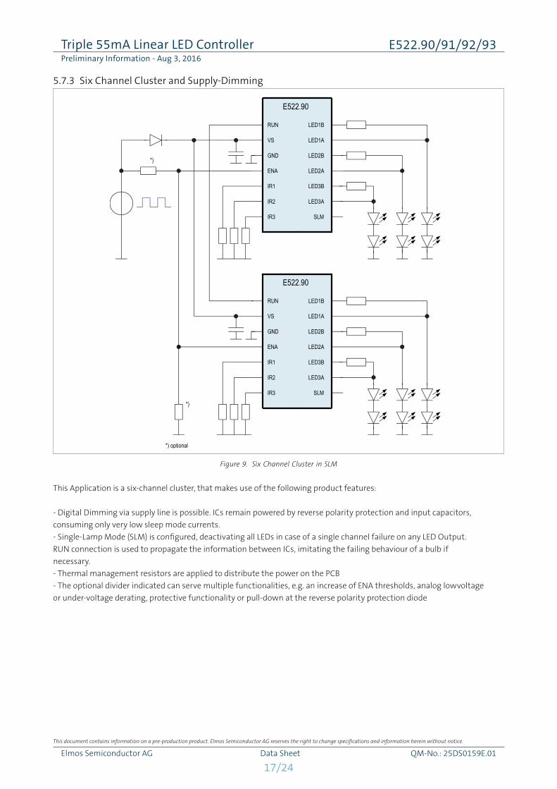
5.7.3 Six Channel Cluster and Supply-Dimming
RUN
VS
GND
ENA
*)
*)
IR1
IR2
IR3
LED1B
LED1A
LED2B
LED2A
LED3B
LED3A
SLM
E522.90
RUN
VS
GND
*) optional
ENA
IR1
IR2
IR3
LED1B
LED1A
LED2B
LED2A
LED3B
LED3A
SLM
E522.90
Figure 9. Six Channel Cluster in SLM
This Application is a six-channel cluster, that makes use of the following product features:
- Digital Dimming via supply line is possible. ICs remain powered by reverse polarity protection and input capacitors,
consuming only very low sleep mode currents.
- Single-Lamp Mode (SLM) is configured, deactivating all LEDs in case of a single channel failure on any LED Output.
RUN connection is used to propagate the information between ICs, imitating the failing behaviour of a bulb if
necessary.
- Thermal management resistors are applied to distribute the power on the PCB
- The optional divider indicated can serve multiple functionalities, e.g. an increase of ENA thresholds, analog lowvoltage
or under-voltage derating, protective functionality or pull-down at the reverse polarity protection diode
18/24
Triple 55mA Linear LED Controller E522.90/91/92/93Preliminary Information - Aug 3, 2016
Elmos Semiconductor AG Data Sheet QM-No.: 25DS0159E.01
This document contains information on a pre-production product. Elmos Semiconductor AG reserves the right to change specifications and information herein without notice.
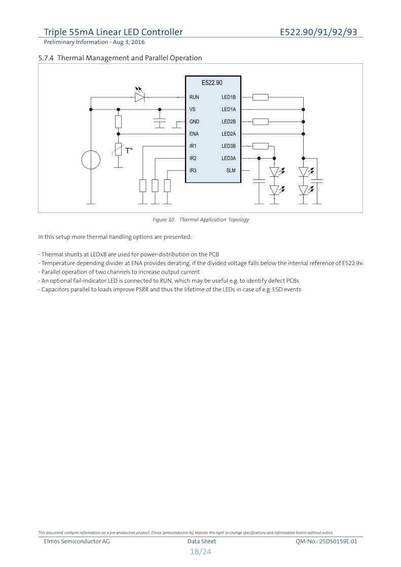
In this setup more thermal handling options are presented:
- Thermal shunts at LEDxB are used for power-distribution on the PCB
- Temperature depending divider at ENA provides derating, if the divided voltage falls below the internal reference of E522.9x
- Parallel operation of two channels to increase output current
- An optional fail-indicator LED is connected to RUN, which may be useful e.g. to identify defect PCBs
- Capacitors parallel to loads improve PSRR and thus the lifetime of the LEDs in case of e.g. ESD events
5.7.4 Thermal Management and Parallel Operation
RUN
VS
GND
ENA
IR1
IR2
IR3
LED1B
LED1A
LED2B
LED2A
LED3B
LED3A
SLM
E522.90
T°
Figure 10. Thermal Application Topology
19/24
Triple 55mA Linear LED Controller E522.90/91/92/93Preliminary Information - Aug 3, 2016
Elmos Semiconductor AG Data Sheet QM-No.: 25DS0159E.01
This document contains information on a pre-production product. Elmos Semiconductor AG reserves the right to change specifications and information herein without notice.
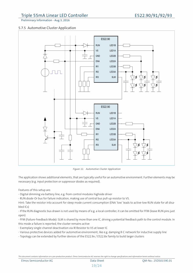
5.7.5 Automotive Cluster Application
RUN
VS
GND
ENA
IR1
IR2
IR3
LED1B
LED1A
LED2B
LED2A
LED3B
LED3A
SLM
E522.90
RUN
VS
GND
ENA
IR1
IR2
IR3
LED1B
LED1A
LED2B
LED2A
LED3B
LED3A
SLM
E522.90
Figure 11. Automotive Cluster Application
The application shows additional elements, that are typically useful for an automotive environment. Further elements may be
necessary (e.g. input protection or suppressor diodes as required).
Features of this setup are:
- Digital dimming via battery line, e.g. from control modules highside driver
- RUN diode-Or bus for failure indication, making use of central bus pull-up resistor to VS.
Hint: Take the resistor into account for sleep mode current consumption (ENA ‘low’ leads to active-low RUN state for all disa-
bled ICs)
- If the RUN diagnostic bus drawn is not used by means of e.g. a local controller, it can be omitted for FFM (leave RUN pins just
open)
- FFM (Failure-Feedback Mode): SLM is shared by more than one IC, driving a potential feedback path to the control module. In
this mode a failure is reported, the cluster remains active
- Exemplary single-channel deactivation via IR Resistor to VS at lower IC
- Various protective devices added for automotive environment, like e.g. damping R-C network for inductive supply line
- Topology can be extended by further devices of the E522.9x / E522.8x family to build larger clusters
20/24
Triple 55mA Linear LED Controller E522.90/91/92/93Preliminary Information - Aug 3, 2016
Elmos Semiconductor AG Data Sheet QM-No.: 25DS0159E.01
This document contains information on a pre-production product. Elmos Semiconductor AG reserves the right to change specifications and information herein without notice.
The following section provides initial dimensioning formulas for E522.9x applications. All values derived in this section must
be verified by suitable prototyping measures.
Typical values for calculations are AI,LEDx/I,IRx = 311 and typ. VIR,NOM generated internally of 1.5V. Details on reference generation
can also be found in „Figure 2. IR Reference Generation“ of chapter „5.3 IR Driver“.
The power shunt RSHUNT located at pin LEDxB is recommended to be calculated from it s maximum static power rating PR,SHUNT.
Please note, that this rating is usually a function of ambient temperature as well. Further details about the thermal distribu-
tion principle can be found in the according chapter „5.2 LED Driver“ and „Figure 1. Power Management Example using a Chan-
nel of E522.9x at 55mA“.
To calculate the power in E522.9x for a typical application, the load voltage VLOAD,LEDx must be taken into account per channel.
The maximum static supply voltage level is assumed to be VVS,MAX. Part of the total power in the linear regulating system is dis-
sipated by RSHUNT. In addition the input reverse-protection diode (e.g. in automotive environments) reduces the input voltage of
E522.9x by it s forward voltage drop (VDIO,REV).
The power formulas are valid, in case the current per channel is fully driven via pin LEDxB through RSHUNT (which should be the
case at VVS,MAX). It is recommended to design the external power shunts in this way. If the devices are operated between VVS,Z1
and VVS,Z2 (see „Figure 1. Power Management Example using a Channel of E522.9x at 55mA“ and according description), make
sure RSHUNT can dissipate sufficient power during input voltage transients higher than VVS,MAX.
If in fact the current is driven by both outputs LEDxA and LEDxB, there is a local maximum of power in E522.9x per channel.
Each local maximum is up to 1/4 of the maximum power the thermal shunt is designed for (see above, e.g. 0.9 * PR,SHUNT).
which can be re-written to
5.8 Dimensioning Formulas and Power Calculation
I LED , x=AI , LEDx/ I , IRx⋅V IR
RIR
RIR=AI , LEDx/ I , IRx⋅V IR
I LED , x
RSHUNT=0.9⋅PR ,SHUNT
I LED2
PE522.9x=(V VS , MAX−V DIO , REV )⋅(∑ I LEDx+I GND ,OP)−∑ PLOAD−∑ PR , SHUNT
∑ P LOAD= I LED1⋅V VLED1+ I LED2⋅V LED2+ I LED3⋅V LED3
∑ P R, SHUNT=I LED12 ⋅RSHUNT1+ I LED2
2 ⋅RSHUNT2+I LED32 ⋅RSHUNT3
21/24
Triple 55mA Linear LED Controller E522.90/91/92/93Preliminary Information - Aug 3, 2016
Elmos Semiconductor AG Data Sheet QM-No.: 25DS0159E.01
This document contains information on a pre-production product. Elmos Semiconductor AG reserves the right to change specifications and information herein without notice.
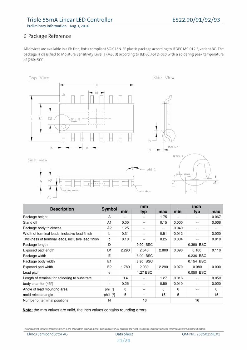
All devices are available in a Pb free, RoHs compliant SOIC16N-EP plastic package according to JEDEC MS-012-F, variant BC. The
package is classified to Moisture Sensitivity Level 3 (MSL 3) according to JEDEC J-STD-020 with a soldering peak temperature
of (260+5)°C.
6 Package ReferenceSpecificationQM-No.:
08SP0637.01
Title:
Package Outline Specification16 lead small outline package (150mil)
with exposed pad(SO16n - ep)
Package Outline and Dimensions are according JEDEC MS-012-F, variant BC.
Description Symbolmm inch
min typ max min typ maxPackage height A -- -- 1.75 -- -- 0.067
Stand off A1 0.00 -- 0.15 0.000 -- 0.006
Package body thickness A2 1.25 -- -- 0.049 -- --
Width of terminal leads, inclusive lead finish b 0.31 -- 0.51 0.012 -- 0.020
Thickness of terminal leads, inclusive lead finish c 0.10 -- 0.25 0.004 -- 0.010
Package length D 9.90 BSC 0.390 BSC
Exposed pad length D1 2.290 2.540 2.800 0.090 0.100 0.110
Package width E 6.00 BSC 0.236 BSC
Package body width E1 3.90 BSC 0.154 BSC
Exposed pad width E2 1.780 2.030 2.290 0.070 0.080 0.090
Lead pitch e 1.27 BSC 0.050 BSC
Length of terminal for soldering to substrate L 0.4 -- 1.27 0.016 -- 0.050
body chamfer (45°) h 0.25 -- 0.50 0.010 -- 0.020
Angle of lead mounting area phi [°] 0 -- 8 0 -- 8
mold release angle phi1 [°] 5 -- 15 5 -- 15
Number of terminal positions N 16 16
Note: the mm values are valid, the inch values contains rounding errorsNote 1: for assembler specific pin1 identification please see QM-document 08SP0363.xx (Pin 1 Specification)
27/03/15 ©Elmos GROUP / Transfer, reproduction, distribution and/or editing, in part or completely, without the priorwritten consent, are prohibited.
Page 1 of 1
22/24
Triple 55mA Linear LED Controller E522.90/91/92/93Preliminary Information - Aug 3, 2016
Elmos Semiconductor AG Data Sheet QM-No.: 25DS0159E.01
This document contains information on a pre-production product. Elmos Semiconductor AG reserves the right to change specifications and information herein without notice.
7 Functional SafetyThe development of this product is based on a process according to an ISO/TS16949 certified quality management system.
Functional safety requirements according to ISO 26262 have not been submitted to Elmos and therefore have not been con-
sidered for the development of this product.
23/24
Triple 55mA Linear LED Controller E522.90/91/92/93Preliminary Information - Aug 3, 2016
Elmos Semiconductor AG Data Sheet QM-No.: 25DS0159E.01
This document contains information on a pre-production product. Elmos Semiconductor AG reserves the right to change specifications and information herein without notice.
8 Record of RevisionChapter Revision Change and Reason for Change Date Released Elmos- .00 Initial revision Feb 15, 2016 DHOE/ZOE
- .01 Product Clasification changed from “Product Preview” to “Prelimi-nary information” Aug 3, 2016 ASU/ZOE
5.5 .01 Text after Figure 5 revised and Table 1 description revised Aug 3, 2016 ASU/ZOE
WARNING – Life Support Applications Policy
Elmos Semiconductor AG is continually working to improve the quality and reliability of its products. Nevertheless, semicon-
ductor devices in general can malfunction or fail due to their inherent electrical sensitivity and vulnerability to physical stress.
It is the responsibility of the buyer, when utilizing Elmos Semiconductor AG products, to observe standards of safety, and to
avoid situations in which malfunction or failure of an Elmos Semiconductor AG Product could cause loss of human life, body
injury or damage to property. In the development of your design, please ensure that Elmos Semiconductor AG products are
used within specifi ed operating ranges as set forth in the most recent product specifi cations.
General Disclaimer
Information furnished by Elmos Semiconductor AG is believed to be accurate and reliable. However, no responsibility is as-
sumed by Elmos Semiconductor AG for its use, nor for any infringements of patents or other rights of third parties, which may
result from its use. No license is granted by implication or otherwise under any patent or patent rights of Elmos Semiconductor
AG. Elmos Semiconductor AG reserves the right to make changes to this document or the products contained therein without
prior notice, to improve performance, reliability, or manufacturability.
Application Disclaimer
Circuit diagrams may contain components not manufactured by Elmos Semiconductor AG, which are included as means of
illustrating typical applications. Consequently, complete information suffi cient for construction purposes is not necessarily
given. The information in the application examples has been carefully checked and is believed to be entirely reliable. However,
no responsibility is assumed for inaccuracies. Furthermore, such information does not convey to the purchaser of the semicon-
ductor devices described any license under the patent rights of Elmos Semiconductor AG or others.
Contact Information
HeadquartersElmos Semiconductor AGHeinrich-Hertz-Str. 1 • D-44227 Dortmund (Germany) : +492317549100 : [email protected] : www.elmos.com
Sales and Application Support Offi ce North AmericaElmos NA. Inc.32255 Northwestern Highway • Suite 220 Farmington HillsMI 48334 (USA) : +12488653200 : [email protected]
Sales and Application Support Offi ce ChinaElmos Semiconductor Technology (Shanghai) Co., Ltd.Unit 16B, 16F Zhao Feng World Trade Building, No. 369 Jiang Su Road, Chang Ning District,Shanghai, PR China, 200050 : +86216210 0908 : [email protected]
Sales and Application Support Offi ce KoreaElmos KoreaB-1007, U-Space 2, #670 Daewangpangyo-ro, Sampyoung-dong, Bunddang-gu, Sungnam-siKyounggi-do 463-400 Korea : +82317141131 : [email protected]
Sales and Application Support Offi ce JapanElmos Japan K.K.BR Shibaura N Bldg. 7F 3-20-9 Shibaura, Minato-ku, Tokyo 108-0023 Japan : +81334517101 : [email protected]
Sales and Application Support Offi ce SingaporeElmos Semiconductor Singapore Pte Ltd.3A International Business Park#09-13 ICON@IBP • 609935 Singapore : +65 6908 1261 : [email protected]
© Elmos Semiconductor AG, 2016. Reproduction, in part or whole, without the prior written consent of Elmos Semiconductor AG, is prohibited.
24/24
Triple 55mA Linear LED Controller E522.90/91/92/93Preliminary Information - Aug 3, 2016
Elmos Semiconductor AG Data Sheet QM-No.: 25DS0159E.01
This document contains information on a pre-production product. Elmos Semiconductor AG reserves the right to change specifications and information herein without notice.


![Amiodarone Treatment in the Early Phase of Acute Myocardial ......overall survival rates in patients with ischemic heart disease [9]. Acute amiodarone treatment inhibits multiple ion-chan-nels,](https://img.pdfslide.us/doc/110x75/6035ad8129eed26d70253d34/amiodarone-treatment-in-the-early-phase-of-acute-myocardial-overall-survival.jpg)