Embed Size (px)
Citation preview

1 of 13 070299
FEATURES§ Real time clock counts seconds, minutes,
hours, date of the month, month, day of theweek, and year with leap year compensationvalid up to 2100
§ 31 x 8 RAM for scratchpad data storage§ Serial I/O for minimum pin count§ 2.0–5.5 volt full operation§ Uses less than 300 nA at 2.0 volts§ Single–byte or multiple–byte (burst mode)
data transfer for read or write of clock orRAM data
§ 8–pin DIP or optional 8–pin SOICs forsurface mount
§ Simple 3–wire interface§ TTL–compatible (VCC = 5V)§ Optional industrial temperature range –40°C
to +85°C§ DS1202 compatible§ Added features over DS1202§ Optional trickle charge capability to VCC1§ Dual power supply pins for primary and
backup power supplies§ Backup power supply pin can be used for
battery or super cap input§ Additional scratchpad memory (7 bytes)
PIN ASSIGNMENT
PIN DESCRIPTIONX1, X2 – 32.768 kHz Crystal PinsGND – GroundRST – ResetI/O – Data Input/OutputSCLK – Serial ClockVCC1, VCC2 – Power Supply Pins
ORDERING INFORMATIONPART # DESCRIPTIONDS1302 Serial Timekeeping Chip;
8–pin DIPDS1302S Serial Timekeeping Chip;
8–pin SOIC (200-mil)DS1302Z Serial Timekeeping Chip;
8–pin SOIC (150-mil)
DESCRIPTIONThe DS1302 Trickle Charge Timekeeping Chip contains a real time clock/calendar and 31 bytes of staticRAM. It communicates with a microprocessor via a simple serial interface. The real time clock/calendarprovides seconds, minutes, hours, day, date, month, and year information. The end of the month date isautomatically adjusted for months with less than 31 days, including corrections for leap year. The clockoperates in either the 24–hour or 12–hour format with an AM/PM indicator.
DS1302Trickle Charge Timekeeping Chip
www.dalsemi.com
VCC2
X1
X2
GND
VCC1
SCLK
I/O
RST
8
7
6
5
1
2
3
4
DS13028-Pin DIP (300-Mil)
VCC2
X1
X2
GND
VCC1
SCLK
I/O
RST
8
76
5
1
2
3
4
DS1302S 8-Pin SOIC (200-Mil)DS1302Z 8-Pin SOIC (150-Mil)

DS1302
2 of 13
Interfacing the DS1302 with a microprocessor is simplified by using synchronous serial communication.Only three wires are required to communicate with the clock/RAM: (1) RST (Reset), (2) I/O (Data line),and (3) SCLK (Serial clock). Data can be transferred to and from the clock/RAM 1 byte at a time or in aburst of up to 31 bytes. The DS1302 is designed to operate on very low power and retain data and clockinformation on less than 1 microwatt.
The DS1302 is the successor to the DS1202. In addition to the basic timekeeping functions of theDS1202, the DS1302 has the additional features of dual power pins for primary and back–up powersupplies, programmable trickle charger for VCC1, and seven additional bytes of scratchpad memory.
OPERATIONThe main elements of the Serial Timekeeper are shown in Figure 1: shift register, control logic, oscillator,real time clock, and RAM. To initiate any transfer of data, RST is taken high and 8 bits are loaded intothe shift register providing both address and command information. Data is serially input on the risingedge of the SCLK. The first 8 bits specify which of 40 bytes will be accessed, whether a read or writecycle will take place, and whether a byte or burst mode transfer is to occur. After the first eight clockcycles have loaded the command word into the shift register, additional clocks will output data for a reador input data for a write. The number of clock pulses equals 8 plus 8 for byte mode or 8 plus up to 248 forburst mode.
COMMAND BYTEThe command byte is shown in Figure 2. Each data transfer is initiated by a command byte. The MSB(Bit 7) must be a logic 1. If it is 0, writes to the DS1302 will be disabled. Bit 6 specifies clock/calendardata if logic 0 or RAM data if logic 1. Bits 1 through 5 specify the designated registers to be input oroutput, and the LSB (bit 0) specifies a write operation (input) if logic 0 or read operation (output) if logic1. The command byte is always input starting with the LSB (bit 0).
DS1302 BLOCK DIAGRAM Figure 1

DS1302
3 of 13
ADDRESS/COMMAND BYTE Figure 2
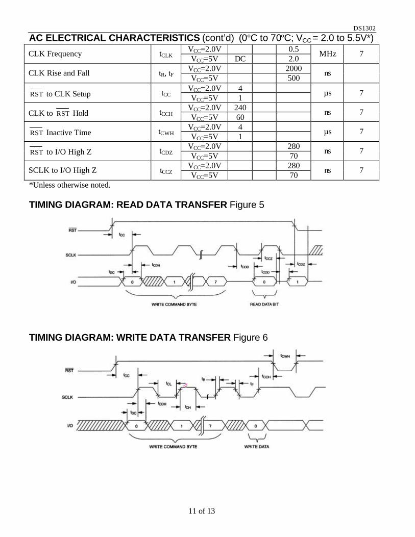
RESET AND CLOCK CONTROLAll data transfers are initiated by driving the RST input high. The RST input serves two functions. First,RST turns on the control logic which allows access to the shift register for the address/commandsequence. Second, the RST signal provides a method of terminating either single byte or multiple bytedata transfer.
A clock cycle is a sequence of a falling edge followed by a rising edge. For data inputs, data must bevalid during the rising edge of the clock and data bits are output on the falling edge of clock. If the RSTinput is low all data transfer terminates and the I/O pin goes to a high impedance state. Data transfer isillustrated in Figure 3. At power–up, RST must be a logic 0 until VCC ] 2.0 volts. Also SCLK must be ata logic 0 when RST is driven to a logic 1 state.
DATA INPUTFollowing the eight SCLK cycles that input a write command byte, a data byte is input on the rising edgeof the next eight SCLK cycles. Additional SCLK cycles are ignored should they inadvertently occur. Datais input starting with bit 0.
DATA OUTPUTFollowing the eight SCLK cycles that input a read command byte, a data byte is output on the fallingedge of the next eight SCLK cycles. Note that the first data bit to be transmitted occurs on the first fallingedge after the last bit of the command byte is written. Additional SCLK cycles retransmit the data bytesshould they inadvertently occur so long as RST remains high. This operation permits continuous burstmode read capability. Also, the I/O pin is tri–stated upon each rising edge of SCLK. Data is outputstarting with bit 0.
BURST MODEBurst mode may be specified for either the clock/calendar or the RAM registers by addressing location 31decimal (address/command bits 1 through 5 = logic 1). As before, bit 6 specifies clock or RAM and bit 0specifies read or write. There is no data storage capacity at locations 9 through 31 in the Clock/CalendarRegisters or location 31 in the RAM registers. Reads or writes in burst mode start with bit 0 of address 0.
As in the case with the DS1202, when writing to the clock registers in the burst mode, the first eightregisters must be written in order for the data to be transferred. However, when writing to RAM in burstmode it is not necessary to write all 31 bytes for the data to transfer. Each byte that is written to will betransferred to RAM regardless of whether all 31 bytes are written or not.
DS1302
4 of 13
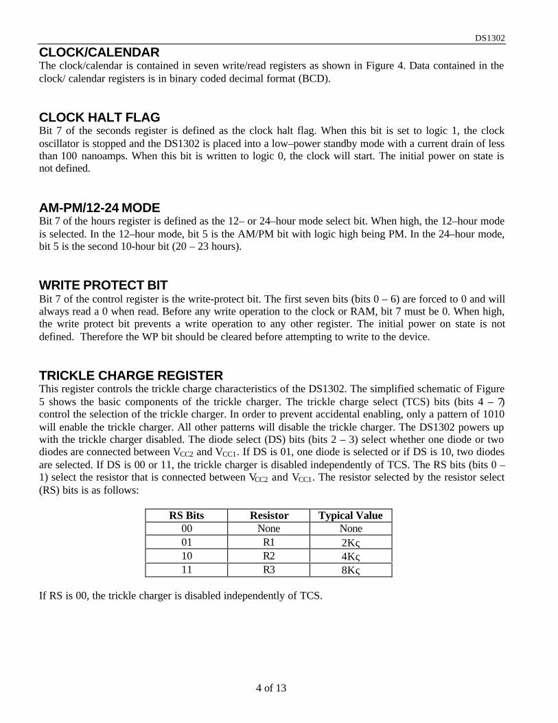
CLOCK/CALENDARThe clock/calendar is contained in seven write/read registers as shown in Figure 4. Data contained in theclock/ calendar registers is in binary coded decimal format (BCD).
CLOCK HALT FLAGBit 7 of the seconds register is defined as the clock halt flag. When this bit is set to logic 1, the clockoscillator is stopped and the DS1302 is placed into a low–power standby mode with a current drain of lessthan 100 nanoamps. When this bit is written to logic 0, the clock will start. The initial power on state isnot defined.
AM-PM/12-24 MODEBit 7 of the hours register is defined as the 12– or 24–hour mode select bit. When high, the 12–hour modeis selected. In the 12–hour mode, bit 5 is the AM/PM bit with logic high being PM. In the 24–hour mode,bit 5 is the second 10-hour bit (20 – 23 hours).
WRITE PROTECT BITBit 7 of the control register is the write-protect bit. The first seven bits (bits 0 – 6) are forced to 0 and willalways read a 0 when read. Before any write operation to the clock or RAM, bit 7 must be 0. When high,the write protect bit prevents a write operation to any other register. The initial power on state is notdefined. Therefore the WP bit should be cleared before attempting to write to the device.
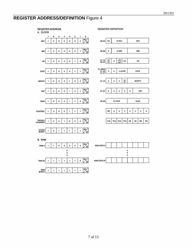
TRICKLE CHARGE REGISTERThis register controls the trickle charge characteristics of the DS1302. The simplified schematic of Figure5 shows the basic components of the trickle charger. The trickle charge select (TCS) bits (bits 4 – 7)control the selection of the trickle charger. In order to prevent accidental enabling, only a pattern of 1010will enable the trickle charger. All other patterns will disable the trickle charger. The DS1302 powers upwith the trickle charger disabled. The diode select (DS) bits (bits 2 – 3) select whether one diode or twodiodes are connected between VCC2 and VCC1. If DS is 01, one diode is selected or if DS is 10, two diodesare selected. If DS is 00 or 11, the trickle charger is disabled independently of TCS. The RS bits (bits 0 –1) select the resistor that is connected between VCC2 and VCC1. The resistor selected by the resistor select(RS) bits is as follows:
RS Bits Resistor Typical Value00 None None01 R1 2Kς10 R2 4Kς11 R3 8Kς
If RS is 00, the trickle charger is disabled independently of TCS.

DS1302
5 of 13
Diode and resistor selection is determined by the user according to the maximum current desired forbattery or super cap charging. The maximum charging current can be calculated as illustrated in thefollowing example. Assume that a system power supply of 5V is applied to VCC2 and a super cap isconnected to VCC1. Also assume that the trickle charger has been enabled with one diode and resistor R1between VCC2 and VCC1. The maximum current Imax would therefore be calculated as follows:
Imax = (5.0V – diode drop) / R1~ (5.0V – 0.7V) / 2Kς
~ 2.2 mA
Obviously, as the super cap charges, the voltage drop between VCC2 and VCC1 will decrease and thereforethe charge current will decrease.
CLOCK/CALENDAR BURST MODEThe clock/calendar command byte specifies burst mode operation. In this mode the first eightclock/calendar registers can be consecutively read or written (see Figure 4) starting with bit 0 of address0.
If the write protect bit is set high when a write clock/calendar burst mode is specified, no data transferwill occur to any of the eight clock/calendar registers (this includes the control register). The tricklecharger is not accessible in burst mode.
RAMThe static RAM is 31 x 8 bytes addressed consecutively in the RAM address space.
RAM BURST MODEThe RAM command byte specifies burst mode operation. In this mode, the 31 RAM registers can beconsecutively read or written (see Figure 4) starting with bit 0 of address 0.
REGISTER SUMMARYA register data format summary is shown in Figure 4.
CRYSTAL SELECTIONA 32.768 kHz crystal can be directly connected to the DS1302 via pins 2 and 3 (X1, X2). The crystalselected for use should have a specified load capacitance (CL) of 6 pF. For more information on crystalselection and crystal layout consideration, please consult Application Note 58, “Crystal Considerationswith Dallas Real Time Clocks."
POWER CONTROLVCC1 provides low power operation in single supply and battery operated systems as well as low powerbattery backup.
VCC2 provides the primary power in dual supply systems where VCC1 is connected to a backup source tomaintain the time and data in the absence of primary power.
The DS1302 will operate from the larger of VCC1 or VCC2. When VCC2 is greater than VCC1 + 0.2V, VCC2
will power the DS1302. When VCC2 is less than VCC1, VCC1 will power the DS1302.

DS1302
6 of 13
DATA TRANSFER SUMMARY Figure 3
DS1302
7 of 13
REGISTER ADDRESS/DEFINITION Figure 4
DS1302
8 of 13
DS1302 PROGRAMMABLE TRICKLE CHARGER Figure 5
DS1302
9 of 13
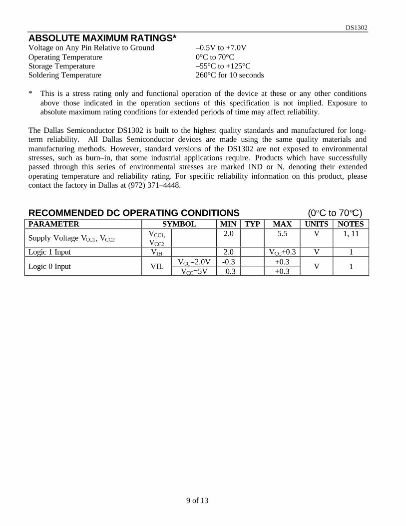
ABSOLUTE MAXIMUM RATINGS*Voltage on Any Pin Relative to Ground –0.5V to +7.0VOperating Temperature 0°C to 70°CStorage Temperature –55°C to +125°CSoldering Temperature 260°C for 10 seconds
* This is a stress rating only and functional operation of the device at these or any other conditionsabove those indicated in the operation sections of this specification is not implied. Exposure toabsolute maximum rating conditions for extended periods of time may affect reliability.
The Dallas Semiconductor DS1302 is built to the highest quality standards and manufactured for long-term reliability. All Dallas Semiconductor devices are made using the same quality materials andmanufacturing methods. However, standard versions of the DS1302 are not exposed to environmentalstresses, such as burn–in, that some industrial applications require. Products which have successfullypassed through this series of environmental stresses are marked IND or N, denoting their extendedoperating temperature and reliability rating. For specific reliability information on this product, pleasecontact the factory in Dallas at (972) 371–4448.
RECOMMENDED DC OPERATING CONDITIONS (0ºC to 70ºC)PARAMETER SYMBOL MIN TYP MAX UNITS NOTES
Supply Voltage VCC1, VCC2VCC1,VCC2
2.0 5.5 V 1, 11
Logic 1 Input VIH 2.0 VCC+0.3 V 1VCC=2.0V -0.3 +0.3Logic 0 Input VILVCC=5V –0.3 +0.3
V 1
DS1302
10 of 13
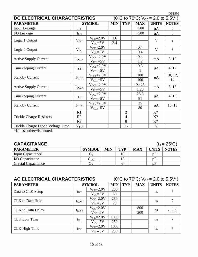
DC ELECTRICAL CHARACTERISTICS (0ºC to 70ºC; VCC = 2.0 to 5.5V*)PARAMETER SYMBOL MIN TYP MAX UNITS NOTESInput Leakage ILI +500 µA 6I/O Leakage ILO +500 µA 6
VCC=2.0V 1.6Logic 1 Output VOH VCC=5V 2.4V 2
VCC=2.0V 0.4Logic 0 Output VOL VCC=5V 0.4V 3
VCC1=2.0V 0.4Active Supply Current ICC1A VCC1=5V 1.2mA 5, 12
VCC1=2.0V 0.3Timekeeping Current ICC1T VCC1=5V 1µA 4, 12
VCC1=2.0V 100Standby Current ICC1S VCC1=5V 100nA 10, 12,
14VCC2=2.0V 0.425Active Supply Current ICC2A VCC2=5V 1.28
mA 5, 13
VCC2=2.0V 25.3Timekeeping Current ICC2T VCC2=5V 81µA 4, 13
VCC2=2.0V 25Standby Current ICC2S VCC2=5V 80µA 10, 13
Trickle Charge ResistorsR1R2R3
248
K?K?K?
Trickle Charge Diode Voltage Drop VTD 0.7 V*Unless otherwise noted.
CAPACITANCE (tA = 25ºC)PARAMETER SYMBOL MIN TYP MAX UNITS NOTESInput Capacitance CI 10 pFI/O Capacitance CI/O 15 pFCrystal Capacitance CX 6 pF
AC ELECTRICAL CHARACTERISTICS (0ºC to 70ºC; VCC = 2.0 to 5.5V*)PARAMETER SYMBOL MIN TYP MAX UNITS NOTES
VCC=2.0V 200Data to CLK Setup tDC VCC=5V 50ns 7
VCC=2.0V 280CLK to Data Hold tCDH VCC=5V 70ns 7
VCC=2.0V 800CLK to Data Delay tCDD VCC=5V 200ns 7, 8, 9
VCC=2.0V 1000CLK Low Time tCL VCC=5V 250ns 7
VCC=2.0V 1000CLK High Time tCH VCC=5V 250ns 7
DS1302
11 of 13
AC ELECTRICAL CHARACTERISTICS (cont’d) (0ºC to 70ºC; VCC = 2.0 to 5.5V*)VCC=2.0V 0.5CLK Frequency tCLK VCC=5V DC 2.0
MHz 7
VCC=2.0V 2000CLK Rise and Fall tR, tF VCC=5V 500ns
VCC=2.0V 4RST to CLK Setup tCC VCC=5V 1
µs 7
VCC=2.0V 240CLK to RST Hold tCCH VCC=5V 60
ns 7
VCC=2.0V 4RST Inactive Time tCWH VCC=5V 1
µs 7
VCC=2.0V 280RST to I/O High Z tCDZ VCC=5V 70
ns 7
VCC=2.0V 280SCLK to I/O High Z tCCZ VCC=5V 70ns 7
*Unless otherwise noted.
TIMING DIAGRAM: READ DATA TRANSFER Figure 5
TIMING DIAGRAM: WRITE DATA TRANSFER Figure 6

DS1302
12 of 13
NOTES:1. All voltages are referenced to ground.2. Logic one voltages are specified at a source current of 1 mA at VCC=5V and 0.4 mA at VCC=2.0V,
VOH=VCC for capacitive loads.3. Logic zero voltages are specified at a sink current of 4 mA at VCC=5V and 1.5 mA at VCC=2.0V,
VOL=GND for capacitive loads.4. ICC1T and ICC2T are specified with I/O open, RST set to a logic “0”, and clock halt flag=0 (oscillator
enabled).5. ICC1A and ICC2A are specified with the I/O pin open, RST high, SCLK=2 MHz at VCC=5V; SCLK=500
kHz, VCC=2.0V and clock halt flag=0 (oscillator enabled).6. RST , SCLK, and I/O all have 40K? pull–down resistors to ground.7. Measured at VIH=2.0V or VIL=0.8V and 10 ms maximum rise and fall time.8. Measured at VOH=2.4V or VOL=0.4V.9. Load capacitance = 50 pF.10. ICC1S and ICC2S are specified with RST , I/O, and SCLK open. The clock halt flag must be set to logic
one (oscillator disabled).11. VCC=VCC2, when VCC2>VCC1 +0.2V; VCC=VCC1, when VCC1>VCC2.12. VCC2=0 volts.13. VCC1=0 volts.14. Typical values are at 25°C.
DS1302 SERIAL TIMEKEEPER 8–PIN DIP (300-MIL)
PKG 8-PINDIM MIN MAX
A IN.MM
0.3609.14
0.40010.16
B IN.MM
0.2406.10
0.2606.60
C IN.MM
0.1203.05
0.1403.56
D IN.MM
0.3007.62
0.3258.26
E IN.MM
0.0150.38
0.0401.02
F IN.MM
0.1203.04
0.1403.56
G IN.MM
0.0902.29
0.1102.79
H IN.MM
0.3208.13
0.3709.40
J IN.MM
0.0080.20
0.0120.30
K IN.MM
0.0150.38
0.0210.53
DS1302
13 of 13
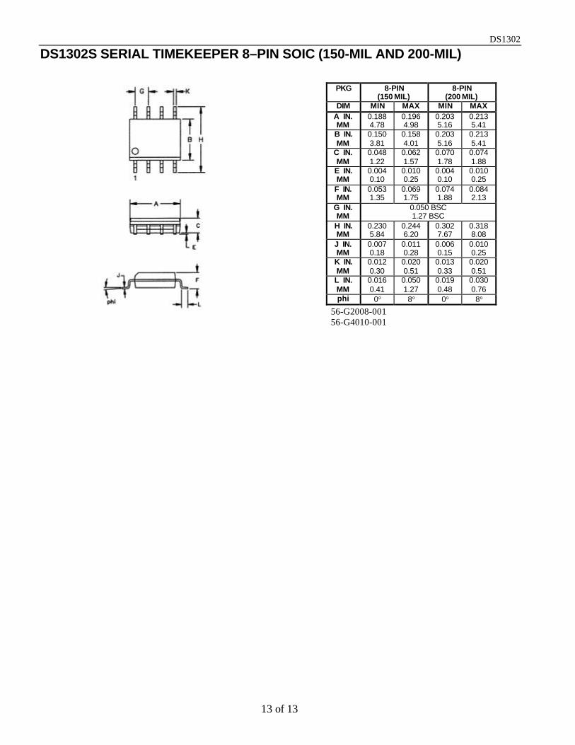
DS1302S SERIAL TIMEKEEPER 8–PIN SOIC (150-MIL AND 200-MIL)
PKG 8-PIN(150 MIL)
8-PIN(200 MIL)
DIM MIN MAX MIN MAXA IN.MM
0.1884.78
0.1964.98
0.2035.16
0.2135.41
B IN.MM
0.1503.81
0.1584.01
0.2035.16
0.2135.41
C IN.MM
0.0481.22
0.0621.57
0.0701.78
0.0741.88
E IN.MM
0.0040.10
0.0100.25
0.0040.10
0.0100.25
F IN.MM
0.0531.35
0.0691.75
0.0741.88
0.0842.13
G IN.MM
0.050 BSC1.27 BSC
H IN.MM
0.2305.84
0.2446.20
0.3027.67
0.3188.08
J IN.MM
0.0070.18
0.0110.28
0.0060.15
0.0100.25
K IN.MM
0.0120.30
0.0200.51
0.0130.33
0.0200.51
L IN.MM
0.0160.41
0.0501.27
0.0190.48
0.0300.76
phi 0° 8° 0° 8°
56-G2008-00156-G4010-001