Embed Size (px)
Citation preview

Transport phenomena in metallic
nanostructures: An ab initio approach
Habilitationsschrift
zur Erlangung des akademischen Grades
Dr. rer. nat. habil.
vorgelegt von
Dr. rer. nat. Peter Zahn
geboren in Jena
Institut fur Theoretische Physik
Fakultat Mathematik und Naturwissenschaften
Technische Universitat Dresden
2003


Fur Manuel und Alexander.


5
Gutachter
1. Gutachter: Prof. K. Becker, TU Dresden
2. Gutachter: Prof. I. Mertig, Martin-Luther Universitat Halle
3. Gutachter: Prof. P. Levy, New York University, USA
4. Gutachter: Prof. W. Butler, University of Alabama, USA
Datum des Einreichens der Arbeit: 4. September 2003


Abstract
A powerful formalism for the calculation of the residual resistivity of metallic nanostructured
materials without adjustable parameters is presented. The electronic structure of the un-
perturbed system is calculated using a screended KKR multiple scattering Green’s function
formalism in the framework of density functional theory. The scattering potential of point
defects is calculated self-consistently by solving a Dyson equation for the Green’s function
of the perturbed system. Using the ab initio scattering probabilities the residual resistivity
was calculated solving the quasiclassical Boltzmann equation. Examples are given for the
resistivity of ultrathin Cu films and the conductance anomaly during the growth of a Co/Cu
multilayer. Furthermore, the influence of surfaces, ordered and disordered interface alloys
and defects at different positions in the multilayer on the effect of Giant Magnetoresistance
is investigated. The self-consistent calculation of the scattering properties and the improved
treatment of the Boltzmann transport equation including vertex corrections provide a power-
ful tool for a comprehensive theoretical description and a helpful insight into the microscopic
processes determining the transport properties of magnetic nanostructured materials.
Kurzfassung
Im Rahmen der vorliegenden Arbeit werden ab initio Berechnungen des Restwiderstandes
von metallischen Nanostrukturen vorgestellt. Die elektronische Struktur der idealen Systeme
wird mit Hilfe einer Screened KKR Greenschen Funktionsmethode im Rahmen der Vielfach-
streutheorie auf der Grundlage der Dichtefunktionaltheorie berechnet. Die Potentiale von
Punktdefekten werden selbstkonsistent mit Hilfe einer Dyson-Gleichung fur die Greensche
Funktion des gestorten Systems berechnet. Unter Nuztung der ab initio Ubergangswahr-
scheinlichkeiten wird der Restwiderstand durch Losung der quasi-klassischen Boltzmann-
Gleichung bestimmt. Ergebnisse fur ultradunne Cu-Filme und die Leitfahigkeitsanomalie
wahrend des Wachstums von Co/Cu-Vielfachschichten werden vorgestellt. Der Einfluß von
Oberflachen, geordneten und ungeordneten Grenzflachenlegierungen und von Defekten an
verschiedenen Positionen in der Vielfachschicht auf den Effekt des Giant Magnetoresistance
wird untersucht. Die selbstkonsistente Berechnung der Streueigenschaften und die verbesserte
Losung der Boltzmann-Transportgleichung unter Einbeziehung der Vertex-Korrekturen stellen
ein leistungsfahiges Werkzeug zur umfassenden theoretischen Beschreibung dar. Sie verhelfen
zu nutzlichen Einsichten in die mikroskopischen Prozesse, die die Transporteigenschaften von
nanostrukturierten Materialen bestimmen.


Contents
1 Introduction 3
2 Formalism 9
2.1 Density functional theory . . . . . . . . . . . . . . . . . . . . . . . . . . . . . 9
2.2 Greens function method and KKR scheme . . . . . . . . . . . . . . . . . . . . 12
2.3 Screened KKR method . . . . . . . . . . . . . . . . . . . . . . . . . . . . . . . 15
2.4 Point defects in metals and T matrix . . . . . . . . . . . . . . . . . . . . . . . 21
3 Transport Theory 25
3.1 Boltzmann theory . . . . . . . . . . . . . . . . . . . . . . . . . . . . . . . . 26
3.2 Transition Probability . . . . . . . . . . . . . . . . . . . . . . . . . . . . . . . 28
3.3 Scattering Anisotropy . . . . . . . . . . . . . . . . . . . . . . . . . . . . . . . 32
3.4 Transport coefficients . . . . . . . . . . . . . . . . . . . . . . . . . . . . . . . . 37
3.5 Kubo vs. Boltzmann formalism . . . . . . . . . . . . . . . . . . . . . . . . . 41
3.6 Fuchs-Sondheimer transport theory . . . . . . . . . . . . . . . . . . . . . . 45
3.7 Landauer formalism . . . . . . . . . . . . . . . . . . . . . . . . . . . . . . . 48
4 Transport in ultrathin films 51
4.1 Introduction . . . . . . . . . . . . . . . . . . . . . . . . . . . . . . . . . . . . . 51
4.2 Ultrathin Cu films . . . . . . . . . . . . . . . . . . . . . . . . . . . . . . . . . 52
4.3 Conductance anomaly during growth . . . . . . . . . . . . . . . . . . . . . . . 53
5 Giant magnetoresistance 59
5.1 Influence of surface scattering . . . . . . . . . . . . . . . . . . . . . . . . . . . 59
5.2 Influence of interface scattering . . . . . . . . . . . . . . . . . . . . . . . . . . 64
5.3 Position and material dependence . . . . . . . . . . . . . . . . . . . . . . . . . 71
6 Summary and outlook 79
1
2 CONTENTS
A Formal solution of Boltzmann equation 81
A.1 Exact solution in k-space . . . . . . . . . . . . . . . . . . . . . . . . . . . . . 81
A.2 Degenerate kernel solution . . . . . . . . . . . . . . . . . . . . . . . . . . . . . 82
A.3 Variational solution . . . . . . . . . . . . . . . . . . . . . . . . . . . . . . . . . 82
A.4 Ziman solution . . . . . . . . . . . . . . . . . . . . . . . . . . . . . . . . . . . 83
List of Figures 85
References 87
Acknowledgment 97
Eidesstattliche Versicherung 99

Chapter 1
Introduction
The information technology revolution is based on an exponential rate of technological
progress. For example, internet traffic doubles every 6 months, wireless capacity doubles ev-
ery 9 months, and magnetic information storage capacity doubles every 15 months. Moore’s
law which indicates that the performance of semiconductor devices doubles every 18 month
has been valid for three decades. But, fundamental laws of physics limit the shrinkage of
semiconductor components on which Moore’s law is based, at least on current technologies.
The continuation of the information technology revolution relies on new ideas for information
storage and processing, leading to future applications. One option is to look for mechanisms
that operate at the nanoscale and exploit quantum effects [1]. Nanotechnology covers a
wide range of different technologies involved in the investigation, manipulation and control
of matter on the very small scale, atom-by-atom and molecule-by-molecule. Such technol-
ogy opens the possibility to develop materials and products with ’nano-scale’ structures or
to build devices and systems the same size as biological cells with highly desirable proper-
ties. It is possible today, to fabricate metallic hybrid structures with dimensions down to
atomic distances in a reproducible manner [2]. Figure 1.1 shows an expressive example of a
sputtered Co/Cu multilayer with a nominal layer thickness of 2nm. Artifical solids can be
prepared by these techniques in complex compositions, different geometries and even in pe-
riodic structures. By the reduced size of the components of the nanostructured systems new
physical properties arise. The surfaces and interfaces are not any more a small perturbation
of the bulk properties. Caused by the quantum properties of the electrons, now surfaces and
interfaces determine the properties of the whole system to a large extent.
In the field of metallic systems layered structures of magnetic and non-magnetic materials
dominated the common interest. In these multilayers ferromagnetic layers are separated by
non-magnetic spacer layers. The phenomenon of interlayer exchange coupling (IEC), discov-
ered 1986 by Grunberg et al., favors one relative orientation of the magnetization direction
of the ferromagnetic layers [4]. That is, forced by the exchange interaction mediated by the
conduction electrons of the non-magnetic spacer layer, the moments of adjacent magnetic
layers are aligned parallel or antiparallel in zero magnetic field. The sign and strength of
the coupling are mainly determined by the material and the thickness of the non-magnetic
3

4 1. INTRODUCTION
Fig. 1.1: Energy filtered transmission electron micrograph of a Co/Cu multilayer with
a nominal layer thickness of 2nm after annealing at 400C, a Cu penetration into a Co
layer is evident in the central region [3]
spacer layer [5, 6]. The thickness of the individual layers is typically in the range of 5 to 100
A, corresponding to 3 to 50 monolayers (ML), and stacks with up to 200 double layers were
prepared. Typically used material combinations are Co/Cu and Fe/Cr, which are favored by
two features. First, their lattice constants and structures fit very well. Second, the electronic
properties of the non-(ferro)magnetic material are very similar to one spin channel of the
magnetic material. This favors the occurrence of the interlayer exchange coupling effect.
Investigating the transport properties of these structures a new phenomenon, the effect of
giant magnetoresistance (GMR) was found in 1988 [7, 8]. This is a drastic change in the
electrical resistivity under an external magnetic field. The magnetic field induces a change
in the relative orientation of the magnetic layers. The GMR systems dominate nowadays
widely the hard disk reading sensor technology, since the stray field of a hard disk causes
this magnetization rotation in highly sensitive layers. The main advantage of GMR systems
with respect to systems exploiting the anisotropic magnetoresistance is the larger signal am-
plitude of the resistivity change and the high potential for sensor miniaturization. Figure 1.2
illustrates the size development of the read heads driven by the exponentially increasing areal
density of magnetic storage. The areal density has been increasing at a compound growth
rate (CGR) of 60% per year since 1991 and 100% since 1998. Other applications in control
and measurement techniques are under development.
The large technological interest on these systems has initiated a large number of experimental
as well as theoretical investigations to elucidate the microscopic origin of the phenomena.
In addition to model calculations ab-initio schemes are of increasing importance for the

1. INTRODUCTION 5
Fig. 1.2: Evolution of IBM hard disk areal density and dimension of read heads [9]
understanding, because they are able to include the material specific properties.
Density Functional Theory (DFT) has been developed to be a powerful tool for the description
of the microscopic electronic structure [10, 11, 12, 13] and the derived macroscopic properties.
It determines the ground state energy of an interacting many-body electron system based on
the electron density instead of using the wave function. In addition to this fundamental
theorem, W. Kohn provided methods which made it possible to set up equations give the
system’s electron density and energy. ”For his development of the density-functional theory”
one half of the Nobel prize in chemistry was awarded to him in 1998 [14].
In contrary to fully quantum-mechanical many-body calculations the numerical effort to solve
the effective one-particle problem is much smaller, but is still determined by the size of the
considered system. In nanostructured materials with a periodicity in certain directions the
size of the problem is determined by the number N of atoms in the unit cell. In systems
without periodicity N is determined by the active region where quantum effects and prop-
erties different from bulk behavior occur. In general, the numerical effort increases with the
third power of N . Even the capability of recent high-performance computer facilities are
overstrained with these demands for complex nanostructures. So, linear scaling electronic
structure codes were developed, which comprise the accuracy of the ab initio methods and
the numerical advantages of tight-binding (TB) methods. This was ultimately necessary for
the description of nanostructured materials with up to 500 atoms per unit cell.
Korringa [15], Kohn and Rostoker [16] (KKR) provided the basis for one of the earliest
and up to now one of the most accurate electronic structure methods. It is a multiple
scattering formalism to determine the Greens function and the eigenfunctions of a given
potential by the superposition of partially scattered waves caused by scattering centers the
potential is devided into. This allows for a separation of the properties of the local scattering
6 1. INTRODUCTION
centers and their geometrical arrangement. In the framework of the TB formulation short
ranged (screened) structure constants are introduced to speed up the scheme. In this work a
TB formulation of the KKR method (Screened KKR) using an appropriate chosen reference
system is applied, which was suggested by ZELLER et al. [17].
In the field of magnetoelectronics the interplay of the spin degree of freedom of the electrons
and the electrical transport properties are of special interest. Microscopic insights into trans-
port phenomena are essential to understand new phenomena and to develop new materials,
functional devices and applications. The most powerful concepts are the so-called quasiclas-
sical or the full quantum-mechanical description. In the first approach electronic structure
is treated quantum-mechanically and the transport coefficients are calculated in a classical
manner solving a kinetic equation for the distribution function of the single-particle states,
called the Boltzmann equation. The fully quantum-mechanical treatment is based on the
Kubo formalism [18]. In both formalisms a linear response to the external field is assumed.
In systems with metallic conductivity this assumption is appropriate. To describe systems
with larger resistivities, where larger voltages have to be applied, non-equilibrium approaches
like the Keldysh Greens function formalism have to be exploited [19].
The transport calculations presented here are based on the quasiclassical approach assuming
diffusive transport in the limit of zero temperature. In contrast to bulk systems nanostruc-
tures contain besides the atomic length scale at least one additional length scale defined by
the dimension of the components. The mean free path of the electrons is the averaged travel-
ing distance between successive scattering events. The quasiclassical approach is valid as long
as the mean free path is larger than the typical diameter of the components and at the same
time shorter than the macroscopic dimension of the device. To solve the Boltzmann equation
the transition probabilities for eigenstates of the unperturbed system have to be provided.
Exploiting the multiple scattering Greens function formalism the scattering potential of given
defects is determined self-consistently. The resulting scattering probability is derived by solv-
ing the Dyson equation for the Greens function of the perturbed system and the scattering
matrix. The resulting electron state-dependent relaxation times and vectors of the mean free
path allow for detailed investigations of the microscopic origins of the resistivity.
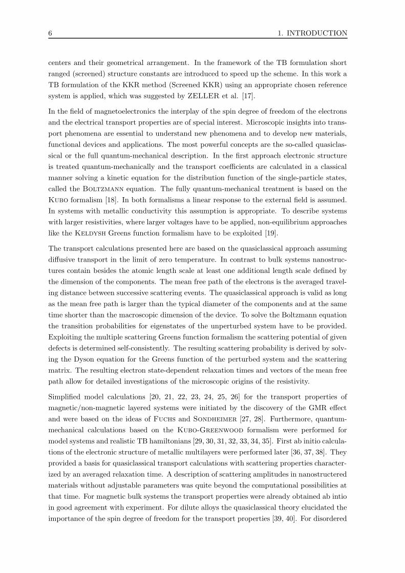
Simplified model calculations [20, 21, 22, 23, 24, 25, 26] for the transport properties of
magnetic/non-magnetic layered systems were initiated by the discovery of the GMR effect
and were based on the ideas of Fuchs and Sondheimer [27, 28]. Furthermore, quantum-
mechanical calculations based on the Kubo-Greenwood formalism were performed for
model systems and realistic TB hamiltonians [29, 30, 31, 32, 33, 34, 35]. First ab initio calcula-
tions of the electronic structure of metallic multilayers were performed later [36, 37, 38]. They
provided a basis for quasiclassical transport calculations with scattering properties character-
ized by an averaged relaxation time. A description of scattering amplitudes in nanostructered
materials without adjustable parameters was quite beyond the computational possibilities at
that time. For magnetic bulk systems the transport properties were already obtained ab intio
in good agreement with experiment. For dilute alloys the quasiclassical theory elucidated the
importance of the spin degree of freedom for the transport properties [39, 40]. For disordered

1. INTRODUCTION 7
alloys with arbitrary concentrations the coherent potential approximation (CPA) was applied
within the quantum-mechanical transport theory to describe the random scattering potential
[41, 42]. The formalism was successfully applied to magnetic multilayers some times later
[43, 44, 45, 46]. This includes the treatment of the scattering properties on the same level as
the ab initio electronic structure. The method does not allow for an easy understanding of
the microscopic processes which cause the macroscopic transport coefficients. The scattering
at lattice imperfections and defects causes a shift in self energy, which is complex, in general.
It requires an additional eigenchannel decomposition of the Greens function to single out the
influence on individual states. The contributions of the eigenstate channels are easily pro-
vided by the quasiclassical theory by the deviation of the single-particle distribution function
from equlibrium.
A formalism calculating the electronic structure and the transport coefficients of layered
nanostructured materials without adjustable parameters will be presented in this work. The
formalism will be applied to ultrathin metallic films with thicknesses of a few atoms. Fur-
thermore, the microscopic origins of the GMR effect will be elucidated. The intrinsic part
of the effect is caused by electronic structure changes connected with the rearrangement of
the magnetic order. In addition, the importance of the extrinsic part of the effect caused by
spin-dependent scattering at magnetic and non-magnetic impurities will be demonstrated.
This work is organized as follows: The basic ideas of Density functional theory and the
KKR-Greens function method are illustrated in Chapter 2. The quasiclassical transport
theory based on the Boltzmann equation is described in detail in Chapter 3. The differ-
ent approximations and computational schemes to solve this equation will be discussed. In
section 3.3 the importance of the vertex corrections in cases of anisotropic scattering will
be illustrated. The equivalence of the quasiclassical theory and the Kubo formula will be
demonstrated for the weak scattering limit in section 3.5. Results for transport phenomena
in ultrathin films are described in Chapter 4. A detailed comparison to experimental results
is given. Ab intio results for the effect of giant magnetoresistance are presented in Chapter
5. The influence of the intrinsic electronic structure, of ordered alloys at interfaces, and of
defects at various positions in the multilayer is discussed. Special emphasis is drawn on the
material dependence of the GMR effect. In the last chapter a summary and prospect to
future developments and investigations are given.


Chapter 2
Density functional theory and KKR
Greens function method
To provide a parameter free description of transport properties of metallic solids several
aspects have to be considered. One of them is the calculation of the electronic structure of the
translational invariant system. For the systems under consideration with a reduced dimension
or a rather complex structure including different materials an efficient calculational scheme is
required. The fundamental concept used for this purpose is density functional theory (DFT).
We will give a short summary of the basics. A comprehensive review of the formal aspects
of density functional theory was given recently by Eschrig [13]. To allow for the treatment
of complex structures with many atoms in the unit cell a numerical scheme scaling linear
with the system size is required. The Screened KKR method meets this requirement and
will be introduced in section 2.3, including test results demonstrating the high accuracy of
the extended scheme. The hierarchy of the KKR Greens function formalism allows for the
treatment of periodic systems and systems with defects on equal footing. The consideration
of perturbed systems is the second ingredient for transport calculations. We focus on the self
consistent determination of the electronic properties of point defects in section 2.4.
2.1 Density functional theory
The Hamilton-operator of a system of N interacting electrons at the positions ri with spin
σi (xi = (ri, σi)) in an external field V (r) is given by
H (x1, . . . , xn) = −N∑
i
∇2ri +
N∑
i,ji6=j
1
|ri − rj|+
N∑
i
V (ri) (2.1)
= T + U + W .
T is the kinetic energy, U the interaction of the electrons and W the potential energy in the
external potential V (r) provided by the nuclei of the atoms. Using the adiabatic approxima-
tion (Born-Oppenheimer) at zero temperature these are considered to be fixed on a lattice.
9

10 2. FORMALISM
Natural units will be used throughout by putting ~ = 2m = ε2
2 = 1. That means, lengths are
given in atomic units, the Bohr radius a0 = 0.529177A, and energies in units of Rydberg
1Ry = 13.6058eV .
The exact solutions of this Hamilton operator are the antisymmetric many-body wave func-
tion |Ψ 〉 which contains all information about the system. But this solution is accessible for
very small systems only. Even if it would be possible to calculate |Ψ 〉 the information would
be very complex. So it was natural to introduce the electron density n(r)
n(r) = 〈Ψ |n|Ψ 〉= 〈Ψ(x1, ..,xN ) |
∑
i
δ(r − ri)|Ψ(x1, ..,xN ) 〉 . (2.2)
The fundamental statement of density functional theory (DFT) is the theorem by Hohen-
berg and Kohn from 1964 [10]: Despite a constant shift the external potential V (r) is
a unique functional of the ground state density n(r). All properties derived from H are
uniquely defined by n(r) using V [n]. The authors introduced a variational principle which
was later generalized by Levy [47] and Lieb [48], which allows to calculate the ground state
energy of a system of N electrons
E0 [V ] = minn(r)|
Rd3rn(r)=N
∫d3rV (r)n(r) + F [n] (2.3)
with a universal functional F [n] which is uniquely defined for all systems described by the
above hamiltonian. As proven by Lieb every (physical meaningful) density n(r) can be
represented by a determinantal fermionic wave function Ψ
n(r) =∑
α
|ψα(r)|2 , (2.4)
using the non-interacting single-particle wave functions |ψα 〉. So the energy functional can
be redefined by
F [n] = T [n] + EH [n] + Exc [n] , with (2.5)
T [n] = −∑
α
〈ψα |∇2r|ψα 〉 , and
EH [n] =
∫∫dr dr′
n(r)n(r′)|r− r′| . (2.6)
T [n] represents the kinetic energy of non-interacting particles of density n(r), EH contains
the Hartree interaction including the self-interaction. Particle conserving variations of the
wave functions |ψα 〉 yield the Kohn-Sham equations
(−∇2r + Veff (r))ψα(r) = Eα ψα(r) , (2.7)
Veff (r) = V (r) + 2
∫dr′
n(r′)|r− r′| +
∂Exc [n]
∂n(r). (2.8)
Under certain conditions the Lagrange multiplier Eα can be interpreted as energy spectrum
of non-interacting quasi-particles described by the |ψα 〉 [12]. These equations have to be

2.1. DENSITY FUNCTIONAL THEORY 11
iterated for a given particle number N =∫drn(r) and external potential V (r) unless self
consistency is achieved. This procedure to find the ground state energy and density of N
electrons in a given external potential is exact, but it requires the knowledge of the exchange-
correlation (xc) potential
Vxc(r) =∂Exc [n]
∂n(r), (2.9)
which is unknown for most systems. The best known system is the homogenous electron gas
for which Vxc and the density εxc of exchange-correlation energy can be evaluated by means
of quantum Monte Carlo calculations as it was done by Ceperley and Alder [49] for the
non-relativistic case and by Kenny et al. for the relativistic case [50]. Adapting this to
systems with a non-homogeneous electron density the local density approximation (LDA) for
the exchange-correlation energy is obtained by
Exc [n] =
∫d3rn(r)εxc(n(r)) , (2.10)
with εxc(n(r)) depending on the density at the position r only. The approximated xc-potential
becomes
Vxc(n(r)) =d
dn(n εxc(n))|n=n(r) . (2.11)
von Barth and Hedin have shown that the Kohn-Sham variational principle can be re-
formulated for the case of magnetic systems by introducing the particle and magnetization
density, respectively [51]
n(r) = n↑(r) + n↓(r) ,
m(r) = n↑(r) − n↓(r) . (2.12)
This yields spin-dependent Kohn-Sham equations
(−∇2 + V σ
eff (r))ψσα(r) = Eσ
α ψσα(r) , (2.13)
with V σxc(r) =
∂
∂nσ
((n↑ + n↓
)εxc(n
↑, n↓))nσ=nσ(r)
, (2.14)
if a spin-diagonal density matrix is assumed. Different parameterizations for εxc(n) and
εxc(n↑, n↓) are proposed in the literature [52, 51, 53]. Throughout this work a parameteri-
zation following Vosko, Wilk, and Nusair [54] was used. Relativistic effects are neglected
because their influence is small for 3d transition metals, which are the main focus concerning
the considered materials.
Using the local density approximation of DFT a large variety of ground state properties of
transition metal bulk materials, molecules and even atoms can be well described despite the
fact that the density is often varying rapidly in space [12]. The reason for this success is
that the exchange-correlation energy is caused mainly by the spherical part of the exchange-
correlation hole due to the isotropy of the Coulomb interaction [55, 56]. This part of the
exchange hole is not so much different for the homogenous and inhomogeneous electron gas.
More difficulties arise in regions with rapidly varying effective potential Vxc(r) like at surfaces
or in systems with localized electrons like atoms.

12 2. FORMALISM
2.2 Greens function method and KKR scheme
Korringa [15], Kohn and Rostoker [16] (KKR) invented one of the earliest, but up to
now one of the most accurate electronic structure method, which is based on the multiple
scattering method first derived by Rayleigh and others [57, 58]. It is a multiple scattering
formalism to determine the Greens function and the eigenfunctions of a given potential by the
superposition of partially scattered waves caused by scattering centers the potential is devided
into. This allows for a separation of the properties of the local scattering centers and their
geometrical arrangement. The electronic properties are derived from the one-particle Greens
function (GF) of the considered system which is characterized by the external potential V (r)
and is divided into a number of non-overlapping scattering centers. Using multiple-scattering
theory the solution of the Schrodinger equation is separated into the single scattering
problem describing the potential properties and the multiple scattering problem reflecting
the structural properties of the system. Dupree [59], Beeby [60] and Holzwarth [61]
extended the method to the treatment of localized defects. In the following years the method
was elaborated further to allow for calculations of periodic crystals and to treat localized
defects [62, 63, 59, 60, 64]. Zeller and Dederichs developed the formalism insofar as self-
consistent calculations of real systems in framework of density functional theory, like defects
in metals, were accessible [65, 66, 67]. The method was extended to the treatment of the
full cell potential [68, 69], the calculation of forces and lattice relaxations [70, 71], surfaces
and layered systems [72, 73], and point defects at surfaces [74, 75, 76]. A special summary of
multiple scattering methods related to KKR is given in the proceedings of a MRS symposium
[77] and a review of the recent conceptual improvements is given in ref. [78].
The problem to solve is the Kohn-Sham equation (2.7) for the one-particle wave functions
for the effective hamiltonian
H(r) = −∇2r + Veff (r) . (2.15)
Instead of solving this equation and summing up the electron density by Eq. (2.4) the same
information is obtained using the one-particle Greens function
(E − H(r))G(r, r′, E) = δ(r− r′) (2.16)
in real space representation at energy E (in general complex). Throughout this section the
spin σ will be omitted for reasons of clarity. For magnetic systems all properties are spin de-
pendent. Using the completeness of the set of eigenfunctions ψα(r) the spectral representation
of the retarded Greens function is obtained
G(r, r′, E) = limγ→+0
∑
α
ψα(r)ψ∗α(r′)E + ıγ − Eα
, (2.17)
which is analytical on the physical sheet of the complex energy plane (Im E ≥ 0). The
particle density is obtained from the diagonal part of the Greens function
n(r, E) = − 1
πIm G(r, r, E) , (2.18)

2.2. GREENS FUNCTION METHOD AND KKR SCHEME 13
which can be used to calculate the particle density instead of evaluating Eq. (2.4)
n(r) =
∫ EF
−∞dE n(r, E) = − 1
π
∫ EF
−∞dE Im G(r, r, E) , (2.19)
with EF the Fermi level. To perform the energy integration efficiently a Fermi-Dirac
distribution function is introduced and the integration path can be shifted into the complex
energy plane including a number of Matsubara poles [74]. This formulation circumvents
the explicit solution of the eigenvalue problem for the determination of the electron density
and is justifying the spirit of density functional theory.
The effective potential Veff (r) is divided into discrete scattering centers, which are assumed
to be non-overlapping. This is achieved by using the full potential approach which treats
the potential in every Wigner-Seitz-cell of the considered system exact including the cell
shape. In contrast, using the muffin tin (MT) or atomic sphere approximation (ASA) instead
a spherical symmetry of the potential inside the sphere around every atomic position Rn is
assumed
V (r) =∑
n
V n(r−Rn) , V n(r) = V n(|r|) =
V n(r) r ≤ Sn
0 r > Sn. (2.20)
with Sn the muffin tin radius or the Wigner-Seitz-radius, respectively. Throughout this
work the ASA approximation will be used.
The eigensolutions of the spherical potentials V n(r) are classified by the angular momentum
quantum number L = (l,m)
RnL(r) = Rn` (r, E)YL (r) ,
HnL (r) = Hn
` (r, E)YL (r) . (2.21)
r denotes the unit vector in direction of r. According to their behavior in the vicinity of the
origin (r → 0) they are called regular and irregular solutions, respectively. The scattering
properties of an isolated potential at given energy E = κ2 are described by the scattering
phase shifts ηn` (E), or likewise by the single-site scattering matrix
tn` (E) =
∫ S
0dr r2j`(κr)V n(r)Rn` (r, E)
= − 1
κsin ηn` (E) eıη
n` (E) , (2.22)
which contains the spherical Bessel function j`(x) as solution for a vanishing potential.
Expanding the Greens function of the system and the δ distribution in terms of the spherical
harmonics
G(Rn + r,Rn′ + r′, E) =∑
LL′Gnn
′LL′(r, r
′, E) YL (r) YL′ (r′) , (2.23)
δ(Rn + r − Rn′ − r′) =1
rr′δnn′ δ(r − r′)
∑
L
YL (r) YL (r′) . (2.24)

14 2. FORMALISM
the so-called structure constants Gnn′LL′(E) of the Greens function are obtained
n = n′ : GnnLL′(r, r
′, E) = δLL′ κ Rn` (r<, E) Hn` (r>, E) , (2.25)
n 6= n′ : Gnn′
LL′ (r, r′, E) = Gnn
′LL′ (E) Rn` (r, E) Rn
′`′ (r
′, E) . (2.26)
The term n = n′ describes the scattering at one center and the second the influence of the
geometrical arrangement of the scattering potentials.
One major advantage of the Greens function method is the hierarchy of the Greens functions
provided by Dyson s equation. Two Greens functions G and G derived from hamiltonians
H and H
H = −∇2r + V , (E − H )G = 1
H = −∇2r + V
= H + ∆V , (E −H )G = 1 , (2.27)
which differ by a potential difference ∆V (r) = 〈 r |∆V | r 〉 only, are connected by a Dyson
equation
G = G + G ∆V G . (2.28)
Using the angular momentum expansion in cell-centered coordinates the single-site and mul-
tiple scattering contributions can be separated and a linear system of equations is obtained
for the structure constants [59, 79, 80]
Gnn′
LL′(E) = Gnn′
LL′ (E) +∑
n′′L′′L′′′Gnn
′′LL′′(E) ∆tn
′′L′′L′′′(E)Gn
′′n′L′′′L′(E) . (2.29)
In the case of spherical scattering potentials the ∆tn matrices are diagonal
∆tnLL′(E) = δLL′(tn` (E)− tn` (E)
)= δLL′∆t
n` (E) . (2.30)
Using a lattice with a basis of N atoms at the positions rµ the site index n in Eq. (2.20) is to
be replaced by an atomic index µ and a cell index n of the unit cell considered. In this case
the structure constants G nn′,µµ′
LL′ (E), the potentials V n,µ(r), and the single site scattering
matrices t n,µ` (E) depend on the combined index (n, µ). For translational invariant system
the potentials and single-site t matrices are independent from the cell index n and a Fourier
transformation with respect to k can be used to transform the algebraic Dyson equation
Gµµ′
LL′(k, E) = Gµµ′
LL′(k, E) +∑
µ′′L′′Gµµ
′′LL′′(k, E)∆tµ
′′`′′ (E)Gµ
′′µ′L′′L′(k, E) . (2.31)
Starting from the free electron gas the structure constants gnn′
LL′ (E) for vanishing potential
are known analytically [81] and the ∆tµ′′`′′ (E) have to be replaced by the t matrices of the
system under consideration. The free space structure constants decay very slowly in real space
(with∣∣∣Rn −Rn′
∣∣∣). So, the determination of the Fourier transformed structure constants
gµµ′
LL′ (k, E) is very time-consuming, despite it can be done very efficiently by the Ewald

2.3. SCREENED KKR METHOD 15
summation technique [62, 82]. To obtain the charge density Eq. (2.31) has to be solved and
an integration in reciprocal space over the Brillouin zone has to be performed.
The matrix equation (2.31) can be solved in a different manner. Omitting the dependence
on k and E and using a matrix notation one obtains
G = [1− g ∆t]−1 G
= [G−1 −∆t]−1
= G− G M−1 G
= −∆t−1 − ∆t−1 M−1 ∆t−1 , (2.32)
with M = G − ∆t−1 .
The solution using the KKR matrix M is most advantageous in the framework of Screened
KKR.
To determine the eigenstates |ψk 〉 of the hamiltonian H the definition of the Greens function
is used
G −1|ψk 〉 = 0 . (2.33)
Furthermore a reference system H is used to reduce the numerical effort to solve this equation.
Using the solution of the Dyson equation (2.29), the angular momentum expansion for the
Greens function in Eq. (2.23), and for the wave function
ψk(Rn + rµ + r) =
∑
L
eıkRnCµL (k) Rµ` (r, E) YL(r) , (2.34)
an algebraic eigenvalue problem for the eigenvector C = CµL (k) is obtained
G−1(1− G∆t) C = 0 , (2.35)
G = Gµµ′LL′(k, E) , ∆t = δLL′ tµ` (E) ,
which contains the structure constants defined in Eq. (2.26) and the difference of the single-
site scattering matrices defined in Eq. (2.30). The index k is a combined index for the wave
vector k and the band index ν. The zeros of the KKR-matrix G(E,k) − ∆t−1(E) define
the single particle eigenvalue spectrum Ek for a given vector k with band index ν. The
eigenvalues of the reference system, determined by det[G−1(E,k)
]= 0, have to be excluded.
As discussed in the next section, a reference system with eigenvalues well above the energy
range of the valence bands is used in the framework of the Screened KKR. This speeds up
the eigenvalue determination, in addition to the advantages in the self-consistency cycle.
2.3 Screened KKR method
Much work was done during the last years to improve the performance of first-principle
calculations based on density functional theory. The aim was to obtain a better scaling of
the numerical effort than the O(N 3) scaling of the traditional electronic structure calculations.

16 2. FORMALISM
Within the traditional KKR scheme the scaling with the cube of N is caused by the matrix
inversion used to solve the Dyson equation (2.29). Due to the long range of the free structure
constants gnn′
LL′ (E) the matrix gµµ′
LL′ (k, E) and so M is dense and requires a large effort for
inversion. In this respect the concept of screening was introduced [83, 84] by which the KKR
method can be transformed into a tight-binding formulation with short-ranged interactions.
It was shown by Andersen et al., that by generalizing the screening concept of the tight-
binding LMTO method to energy-dependent screening parameters and by optimizing these
parameters exponentially decaying structure constants can be obtained [83]. This concept was
implemented for surfaces and interfaces by Szunyogh et al. [85] and successfully applied to
relativistic ab intio calculations of surfaces [86, 87]. Unfortunately, the decay of the screened
structure constants obtained by this optimization procedure was not sufficiently fast and
limited the accuracy of the method.
Fig. 2.1: Reference system of muffin-tin potentials of constant hight
A physically and mathematically more simple and transparent method to obtain a tight-
binding form of the KKR method was suggested by Zeller et al. [17], and is based on the
concept of a favorably chosen reference system. The implementation used is this work is based
on this concept, which will be sketched briefly. One has to emphasize that the reformulation
using the reference system is an exact transformation of the formalism and the accuracy of
the Screened KKR method can be tailored by the properties of the reference system to the
same level as the primary KKR scheme. Furthermore, in the Screened KKR scheme there are
no restrictions concerning the properties of the real system as in the classical TB methods or
methods based on the short ranged density matrix [88].
Beside the construction of the free structure constants the main numerical effort is required
to solve the Dyson equation (2.29). This equation can be replaced by two equations of the
same structure by introducing a reference system, labeled by a tilde in the following
G = g + g t G , (2.36)
G = G + G ∆t G , (2.37)
with ∆t = t − t .
The geometrical structure of the reference system has to be the same as the system under
consideration and it is assumed that the starting point of the calculation is the free space.
This formulation is an exact transformation done without any additional approximation. By

2.3. SCREENED KKR METHOD 17
choosing the single-site t matrices t = tn` (E) appropriate the screening of the structure
constants G = Gnn′LL′ (E) can be tuned. For self-consistent electronic structure calculations
the Greens function has to be determined for energies typically below 1 Rydberg. By choosing
the reference system without eigenstates in that energy range the desired exponential decay
can be obtained. A particular choice of the reference system is sketched in Fig. 2.1. It is an
infinite array of repulsive, constant potentials of height Vshf within non-overlapping spheres
around each scattering center and zero potential in the interstitial region. Another possibility
is to choose potential wells of infinite height. The eigenstates of these reference systems are
shifted to higher energy in comparison to the free space. Figure 2.2 summarizes the behavior
0.5 1 2 4 8 16 32 INF64 128Vshf [Ry]
0.5
1
2
34567
EB
ot,l [R
y] lmax = 3lmax = 3lmax = 4lmax = 4lmax = 6lmax = 6
Fig. 2.2: Band bottom EBot,` of reference systems containing muffin-tin potentials of
constant height Vshf and infinite height (∞)
of the bottom of the bands of the reference systems in dependence on the potential height
Vshf and maximum angular momentum `max choosing touching muffin-tin spheres. For not
to high potentials first-order perturbation theory indicates that the shift of the eigenstates
is proportional to the potential height times the space filling of the spheres. This behavior
can be recognized in Fig. 2.2 for potentials smaller than 4 Ry. For higher potentials the
values saturate. The maximum is obtained for the reference potentials of infinite height and
it depends on the `max-cut-off of the Greens function expansion. The limit for `max →∞ for
a Cu lattice (fcc structure, lattice constant 6.76a.u.) is estimated to be around 7.5Ry. This
value depends on the crystal structure and space filling of the reference potentials and scales
inversely with the lattice constant squared. For energies well below the lowest eigenstate of
the reference system the structure constants G = Gnn′LL′ (E) indeed decay exponentially with
the real space distance [17, 89]. By choosing the reference potentials sufficiently high (larger
about 4 Ry) this behavior is obtained for the whole energy range involved in the calculation
of the valence electron density.
By solving Eq. (2.36) the screened structure constants are obtained. Exploiting the short-
ranged character of them, the solution of this equation can be done in real space on a finite
cluster enclosing Nc sites Rn. This circumvents the calculation of the Fourier transformed
free structure constants. In general, the system under consideration has extended states and
the Greens function is long-ranged. So, Eq. (2.37) has to be solved in reciprocal space and the

18 2. FORMALISM
screened structure constants can be Fourier transformed with negligible effort, because the
real space sum is limited by the number of sites in the cluster used to solve Eq. (2.36). This
scheme is exceptional advantageous for systems with a complex structure and many atoms
in the unit cell. Caused by the finite range of the real space structure constants Gnn′
LL′ (E)
only couplings with a finite range occur in the Fourier transformed structure constants
Gµµ′
LL′(k, E).
System Unit Cell Gµµ′
LL′ Effort
Wire ∝ N2 ... 2.3
Multilayer ∝ N
Fig. 2.3: Non-zero (LL′)-blocks in screened structure constant matrix Gµµ′
LL′(k, E) and
numerical effort for different geometries
Especially for layered systems described by large prolonged unit cells the occurring elements
are restricted to regions close to the main diagonal. This is similar to the tight-binding
hamiltonian matrix of a one-dimensional system. The dots in Fig. 2.3 symbolize blocks of the
dimension ((`max+1)2× (`max+1)2) connecting sites µ and µ′ in the unit cell. By combining
a number of sites to one principal layer one can obtain that only neighboring principle layers
couple. The matrix Gµµ′
LL′(k, E) in the generalized principle layer indices becomes tridiagonal
or cyclic tridiagonal form. For this type of matrices efficient algorithms were implemented
to calculate the diagonal elements of the inverse matrix entering Eq. (2.32) to obtain the
electron density using Eq. (2.18). The numerical effort for this type of systems scales linearly
with the number N of atoms in the unit cell. A small overhead due to the calculation of the
screened structure constants on the finite clusters occurs, but even for systems with about
10 atoms the total numerical effort is less than with the traditional KKR scheme. This is
illustrated in Fig. 2.4. The scaling with the `max-cut-off of the angular momentum expansion
of the Greens function is proportional to the cube of (`max+1)2 stemming from the treatment
of the super-blocks.
For systems with a one-dimensional geometry the shape of the unit cell is disk like, as shown
in Fig. 2.3. The non-zero blocks in the matrix Gµµ′
LL′(k, E) are distributed equally, but for large

2.3. SCREENED KKR METHOD 19
2 4 8 16 32 64N
0
20
40
60
T [s
]
TTB, lmax=2TTB, lmax=3TTB, lmax=4TSt
Fig. 2.4: Computing time TTB for solving the Dyson equation as a function of N the
number of layers in the slab: time in seconds per k-point on an IBM-390H-Workstation,
for comparison with standard KKR (`max = 3, TSt ∝ N 3)
systems their density is small. Efficient sparse-matrix techniques were designed on the basis
of algorithm from the literature [90, 91] which exploit explicitely the block-sparse character
of the matrix. The scaling is approximately proportional to the square of N , and depends
slightly on the geometrical structure and dimensions of the unit cell.
322 4 6 8 16 INF1Vshf [Ryd]
10−5
10−4
10−3
10−2
∆c
l=3, R=0.77 RMT
l=4, R=0.81 RMT
l=5, R=0.82 RMT
l=3, R=RMT
l=4, R=RMT
l=5, R=RMT
Fig. 2.5: Deviations of the numerically determined eigenvectors of free electrons from
the exact result (Eq. (2.38)) at fixed energy E = 0.5Ryd as a function of Vshf and the
`max-cut-off; open symbols for muffin tin potentials of finite height, closed symbols for
potentials of infinite height with optimized radii; arrows indicate the optimum with
respect to Vshf ; cluster size is 79, from [92]

20 2. FORMALISM
The case of a vanishing Potential V = 0 is a challenging test for every method with localized
orbitals. It is well known that the standard KKR [93] and the screened KKR with finite
reference potentials [17, 94] fulfill the empty lattice test and give exact results for band
structure and density of states. The accuracy will be demonstrated in Fig. 2.5 by comparing
the eigenvectors obtained in Eq. (2.35) for a free electron gas with the analytically known
expansion coefficients (see ref. [81]) in dependence on the chosen reference system and the
maximum angular momentum `max. Results for the deviation of the obtained expansion
coefficients
∆c =
`max∑
`=0
|C`(E) − C`(E)| (2.38)
are shown for muffin tin reference potentials of different height and infinite high potentials
with an optimized radius [92]. The size of the cluster to calculate the reference structure
constants by Eq. (2.36) was fixed to 79 sites on a face-centered-cubic lattice. The optimum
for a fixed `max is marked by an arrow and is caused by two reasons: (1) for small potentials
the screening of the reference structure constants is weak and the real space solution of
Eq. (2.36) introduces systematic errors. (2) For higher reference potentials the deviations
increase because of the finite `max cut-off used, which prevents the description of the strong
angular variation of the wave functions next to the touching points of the spheres with high
potential. So the optimum for the reference system is to use either muffin-tin spheres of
medium height, e.g. 4 Ry, or infinitely high potentials with a reduced radius, about 20 %
smaller than the muffin-tin radius.
Another accuracy demonstration of the method is given in Fig. 2.6 by the deviation of energy
eigenvalues obtained from the zeros of Eq. (2.33) for a free electron gas on a body-centered-
cubic parent lattice. The deviation ∆Ek for a fixed wave vector ( 12 ,
12 , 0)2π
a is given as a
function of the height and the radius of the used reference system, and in addition on the
size Nc of the cluster used to determine the reference Greens function in real space. The
precision rises by about 4 orders of magnitude by increasing the cluster size from Nc = 15 to
Nc = 169. The higher effort to solve Eq. (2.37) is justified by the obtained accuracy of about
10−6Ry.
The method in it’s present form is able to treat system of various geometries. The self consis-
tent calculation of multilayers, either periodic (bulk) or finite (slabs) in direction perpendicu-
lar to the layers, interfaces and surfaces of complex structure, and quasi one-dimensional sys-
tems is feasible. The method was successfully applied to the calculation of periodic multilayer
systems with ideal interfaces [94], finite multilayers [95], multilayers including ordered alloys
[96], free-standing nanowires [97, 98], monoatomic rows on vicinal surfaces [99], magnetic
anisotropies of surfaces, including ordered and disordered metal overlayers [100, 101, 102].
It has to be pointed out, that the transformation on the screened structure constants is exact
and that the method works for all materials, i.e. metals, semiconductors, and insulators.
This is in contrast to other modern O(N) methods which gain their advantage essentially
from the short-ranged behavior of the density matrix of the system under consideration,
recently reviewed by Goedecker [88]. The short-range interactions in the screened KKR
2.4. POINT DEFECTS IN METALS AND T MATRIX 21
0,75 0,8 0,85 0,9 0,95 1R/RMT
10-6
10-5
10-4
10-3
∆Ek [Ry]
Vshf=2RyVshf=4RyVshf=8RyVshf=16RyVshf=32RyVshf=128RyVshf=∞
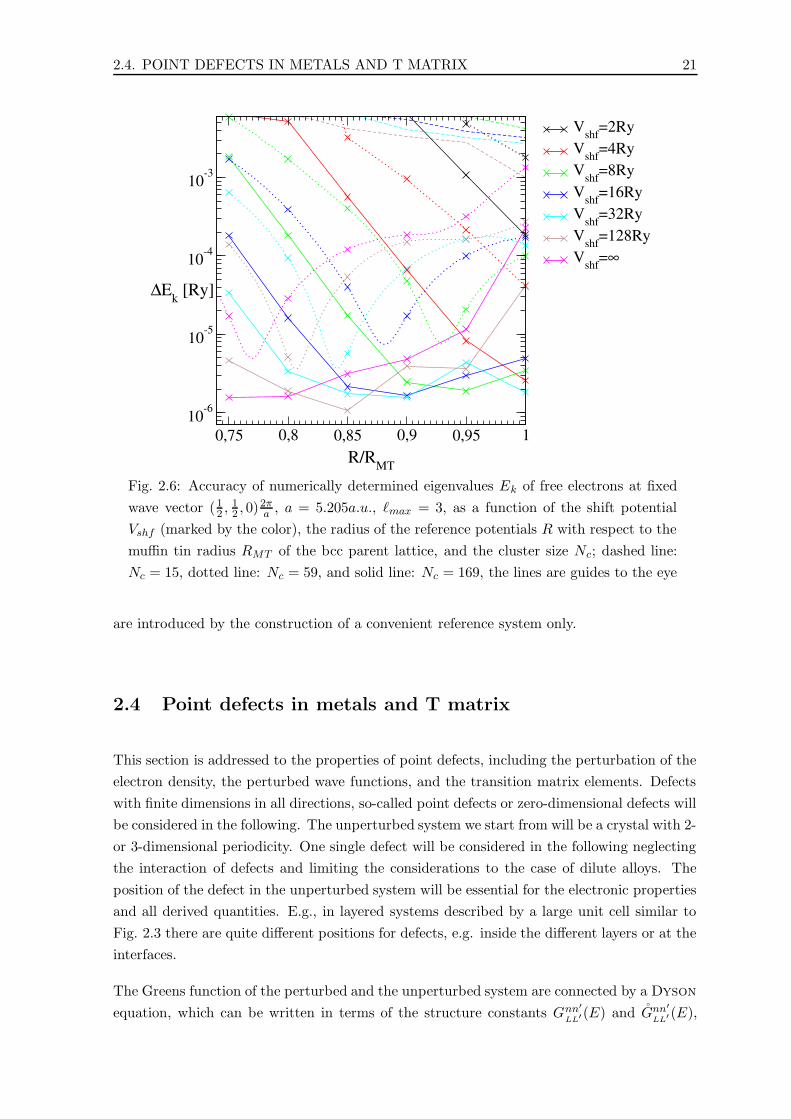
Fig. 2.6: Accuracy of numerically determined eigenvalues Ek of free electrons at fixed
wave vector ( 12 ,
12 , 0)2π
a , a = 5.205a.u., `max = 3, as a function of the shift potential
Vshf (marked by the color), the radius of the reference potentials R with respect to the
muffin tin radius RMT of the bcc parent lattice, and the cluster size Nc; dashed line:
Nc = 15, dotted line: Nc = 59, and solid line: Nc = 169, the lines are guides to the eye
are introduced by the construction of a convenient reference system only.
2.4 Point defects in metals and T matrix
This section is addressed to the properties of point defects, including the perturbation of the
electron density, the perturbed wave functions, and the transition matrix elements. Defects
with finite dimensions in all directions, so-called point defects or zero-dimensional defects will
be considered in the following. The unperturbed system we start from will be a crystal with 2-
or 3-dimensional periodicity. One single defect will be considered in the following neglecting
the interaction of defects and limiting the considerations to the case of dilute alloys. The
position of the defect in the unperturbed system will be essential for the electronic properties
and all derived quantities. E.g., in layered systems described by a large unit cell similar to
Fig. 2.3 there are quite different positions for defects, e.g. inside the different layers or at the
interfaces.
The Greens function of the perturbed and the unperturbed system are connected by a Dyson
equation, which can be written in terms of the structure constants Gnn′LL′(E) and Gnn
′LL′ (E),

22 2. FORMALISM
respectively
Gnn′
LL′(E) = Gnn′
LL′ (E) +∑
n′′L′′Gnn
′′LL′′(E) ∆tn
′′`′′ (E)Gn
′′n′L′′L′(E) , (2.39)
assuming spherical potentials (ASA). The reference system G is now the periodic system
without defect and G describes the system with one defect at a specific position µ0. The
explicit dependence on µ0 will be suppressed in the following. The difference of the single-site
scattering matrices ∆tn′′`′′ (E) describes the potential perturbation caused by the defects. Due
to the effective screening of the perturbation in metallic systems the charge and magnetization
deviations are restricted mainly to the vicinity of the defect. The solution of Eq. (2.39) will
be restricted to a number of neighboring sites next to the defect. Using the Greens function
G of the perturbed system the changes in charge and magnetization density can be calculated
and allow for a self consistent electronic structure calculation.
The perturbation of the potential ∆V causes scattering processes of the unperturbed Bloch
states which keep the spin and the energy unchanged. The neglect of spin-flip processes is
justified by experimental results that in 3d transition metals the scattering cross section for
these processes is about 2 orders of magnitude smaller than for spin-conserving processes
[103]. The scattering at the potential perturbation ∆V can be expressed by the transition
operator T
∆V G = T G , (2.40)
∆V |ψk 〉 = T | ψk 〉 , (2.41)
T = ∆V(
1− G∆V)−1
(2.42)
= ∆V(
1 + G∆V),
providing that |ψk 〉 can be calculated from | ψk 〉 by a Lippman -Schwinger equation.
The single-particle wave function of the unperturbed system is a Bloch wave characterized
by the angular momentum expansion coefficients CµL (k)
〈Rn + rµ + r || ψk 〉 = ψk(Rn + rµ + r) =
1√V
∑
L
C n,µL (k) Rµ` (r, E) YL(r) ,
with C n,µL (k) = eıkRn
CµL (k) , (2.43)
and V the normalization volume of the wave function. The spin index for magnetic systems
and the explicit energy dependence of the wave functions will be dropped throughout this
section for the sake of simplicity. In contrast, the perturbed wave function of the system with
defect depends on the position of the defect in the unit cell µ0 and is not even more a single
Bloch state
ψk(Rn + rµ + r) =
1√V
∑
L
C n,µL (k) Rµ` (r, E) YL(r) , (2.44)
which means that the C n,µL (k) depend strongly on the cell index n. The perturbed and
unperturbed wave functions are connected by a Lippman -Schwinger equation including the

2.4. POINT DEFECTS IN METALS AND T MATRIX 23
Greens function of the unperturbed system and the potential difference. This can be expressed
in terms of the structural Greens function matrix G =G nn′,µµ′
LL′
and the difference of the
single-site t matrices using Eq. (2.30)
C n,µL (k) =
∑
n′µ′L′D nn′,µµ′
LL′ (E) C n′,µ′
L′ (k) , (2.45)
with D nn′,µµ′
LL′ (E) =[1− G∆t
]−1nn′,µµ′
LL′ (2.46)
=[1 +G∆t
]nn′,µµ′
LL′ .
The summation is restricted to sites (n′, µ′) in the vicinity of the defect.
Now the matrix elements of the transition operator T can be expressed in terms of the
potential perturbation and the unperturbed Bloch states
Tkk′ = 〈 ψk |∆V |ψk′ 〉 = 〈 ψk |T | ψk′ 〉 (2.47)
=
∫d3rψ∗k(r)∆V (r)ψk′(r) . (2.48)
Using the angular momentum expansion of the wave functions in Eq. (2.43) and Eq. (2.45)
the matrix element is obtained by
Tkk′ =1
V
∑
nµL
C∗ n,µL (k)∆ n,µL (E)C n,µ
L (k′) , (2.49)
with ∆ n,µL (E) = e−2ıηµ` (E)∆t n,µL (E) , (2.50)
and ηµ` (E) the scattering phase shifts of the unperturbed system. Using the angular momen-
tum expansion of the transition operator
T nn′,µµ′
LL′ (E) = ∆ n,µL (E)D nn′,µµ′
LL′ (E) , (2.51)
and the generalized wave function coefficients
Q n,µL (k′) =
∑
n′µ′L′T nn′,µµ′
LL′ (E) C n′,µ′
L′ (k′) , (2.52)
the matrix elements Tkk′ can be expressed as
Tkk′ =1
V
∑
nn′µµ′LL′C∗ n,µL (k) T nn′,µµ′
LL′ (E)C n′,µ′
L′ (k′) (2.53)
=1
V
∑
nµL
C∗ n,µL (k)Q n,µL (k′) . (2.54)
This formalism describes the potential scattering of electrons, which is elastic by definition,
caused by point defects without adjustable parameters. It provides the basis for transition
probabilities and scattering cross sections entering the transport theory. The derivation of
these quantities will be described in section 3.2.


Chapter 3
Transport theory
In this chapter the fundamentals of the transport theory used in the calculations will be
sketched. The different solutions of the linearized Boltzmann equation will be introduced,
the microscopic description of the scattering probability amplitude, the anisotropy of the
scattering, and the resulting conductivity will be discussed. The phenomenon of giant Mag-
netoresistance (GMR) will be introduced.
To describe the transport coefficients from ab initio theory one has two general options. One
is based on Kubos linear response formalism [18, 104], which was adapted to the conductivity
of disordered alloys [105, 106], and was successfully applied to bulk and multilayer materials
[41, 44, 107, 108, 109]. The method does not allow for an microscopic understanding of the
processes which cause the macroscopic transport coefficients. This is the major advantage
of the semiclassical Boltzmann formalism. It allows for a detailed characterization of the
microscopic scattering processes and the dependence on the electronic structure of host and
defects.
To describe the transport properties of layered structures a semiclassical approach based on
the formalism of Fuchs and Sondheimer was introduced and applied to the GMR effect
[20, 21, 22, 23, 24, 25]. The validity of this model is limited by the basic assumption that the
mean free path of the electrons is larger than the thickness of a single layer. For most of the
experimentally investigated systems this is not given. The decay of the GMR ratio for very
large layer thicknesses is reproduced by these models. The basic ideas of the model will be
sketched in section 3.6.
To describe the GMR for the current-perpendicular-to-layer geometry the Landauer ap-
proach was adapted to investigate the influence of the coherent electronic structure of the
system [38] and the influence of scattering centers in the layers [110, 111, 108]. The formalism
will be outlined in section 3.7.
The equivalence of the semiclassical Boltzmann approach to the fully quantum-mechanically
Kubo formalism will be shown in section 3.5, and the limits for the applicability will be
formulated.
25

26 3. TRANSPORT THEORY
3.1 Boltzmann theory
The Boltzmann theory is based on a classical distribution function fk(r, t) which gives
the number of carriers in quantum-mechanical state k, and can depend on the position in
real space r, too. k denotes the wave vector k and the band index ν. In the following
derivations the spin is neglected for the sake of simplicity and an explicit dependence of the
distribution function on time and magnetic field are excluded. The real space dependence
vanishes due to the restriction to homogenous systems. In the steady state the total rate of
change has to vanish, and from the conservation of phase space volume a master equation
for the distribution functions is derived
dr
dt
∂fk∂r
+dk
dt
∂fk∂k− ∂fk
∂t
∣∣∣∣scatt
= 0 . (3.1)
It describes the partial changes of the distribution function due to diffusion, the influence
of external fields and scattering processes. The first term describes the diffusion due to the
group velocity of the carriers. For homogeneous electric fields, that means on the length scale
of the mean free path, the diffusion term can be neglected. The mean free path has to be
larger than the periodicity of the structure, what is given in the weak scattering limit. The
second term is determined by the external electric field E with e the electron charge e = − |e|
k = eE . (3.2)
Introducing the velocity of the carriers by the group velocity of the states k one arrives at
k∂fk∂Ek
∂Ek∂k− ∂fk
∂t
∣∣∣∣scatt
= 0 with vk =∂Ek∂k
. (3.3)
The third term in Eq. (3.1) describes the change of carriers in state k due to scattering, and
is related to the microscopic transition probability Pkk′ [Eq. (3.13)] by
∂fk∂t
∣∣∣∣scatt
=∑
k′fk′ (1− fk)Pk′k − fk
(1− f ′k
)Pkk′ . (3.4)
The second term is the scattering out term, which counts the carriers which are scattered
out of the state k and the first, the scattering-in term counts the reverse processes. These
processes can be caused, e.g. by lattice defects, imperfections or thermally activated quasi
particles.
The distribution function in the steady state will be split up into the equilibrium distribution
function fk given by the Fermi-Dirac distribution at temperature T and a perturbation gk
fk = fk + gk with fk =
(eEk−µkBT + 1
)−1
. (3.5)
Exploiting the microscopic reversibility Pkk′ = Pk′k and considering energy conserving scat-
tering processes only [Eq. (3.13)] the change of the distribution function due to scattering is
given by
∂fk∂t
∣∣∣∣scatt
=∑
k′Pkk′ (gk′ − gk) . (3.6)

3.1. BOLTZMANN THEORY 27
In the limit of linear response the proportionality of gk and the external field E is given by
the vector mean free path Λk using the ansatz
gk = −e∂fk∂E
ΛkE . (3.7)
Neglecting higher order terms in E one obtains with Eq. (3.3) and Eq. (3.6) the linearized
Boltzmann equation
vk =∑
k′Pkk′ (Λk −Λk′) . (3.8)
Introducing the Boltzmann relaxation time
τBk =
[∑
k′Pkk′
]−1
, (3.9)
this can be expressed by
Λk = τBk
[vk +
∑
k′Pkk′Λk′
]. (3.10)
The first term on the r.h.s describes the means free path in relaxation time approximation
known from textbooks, which describes the distance between two successive scattering events
out of the state k. The second term on the r.h.s. is the so-called scattering-in term which
counts the scattering events from state k ′ back to the considered state k. It causes the vertex
corrections in the expansion of the mean free path. As will be shown in section 3.3, only the
antisymmetric part PAkk′ of the transition probability contributes to this term. In the limit of
well defined bands (dilute alloys or weak scattering) it will be shown that the conductivity
tensor using this solution is the same as that obtained by the Kubo-Greenwood formalism.
The Boltzmann equation is a coupled integral equation to determine the vector of mean
free path, where the integration has to be performed over the states with a given energy.
In the limit of zero temperature this has to be done for the states on the anisotropic Fermi
surface of the system under consideration. This case will be considered in the next section.
For magnetic systems the spin variable σ has to be considered, which can easily be included
formally by k = (k, ν, σ). For the discussion of non spin-conserving scattering processes see
section 3.2. In the following, the iterative and the relaxation time solutions for Eq. (3.10)
will be sketched briefly. Other schemes for the solution are discussed in appendix A.
3.1.1 Iterative solution
The iterative scheme to solve Eq. (3.10) was proposed by Colerigde and implemented first
by v. Ek and Mertig [112, 113, 39] for point defects in bulk materials. As a starting
point for the vector of mean free path Λk on the r.h.s. of the Boltzmann equation (3.10)
one can use the relaxation time approximation in Eq. (3.11) or the Ziman solution from
Eq. (A.15). Iterating with this starting point one can achieve convergence for the l.h.s of
28 3. TRANSPORT THEORY
Eq. (3.10) within at least 10 iterations. In all calculations of the present work this scheme
was used. A convergence quality for the relative deviation of the vector mean free path
from one to the next iteration of 10−5 was achieved for system with a resistivity larger than
1µΩcmat%. In the other cases the matrix τP with τ defined in Eq. (A.1) is relatively large
and has eigenvalues with an absolute value close to 1. This is caused by large anisotropies
in the scattering probability due to weak scattering. In these cases the forward scattering is
dominating One has to keep in mind that the matrix P in Eq. (3.10) is determined by the
antisymmetric part PAkk′ of the transition probability matrix defined in Eq. (3.27), whereas
the relaxation times τBk are determined by the symmetric part P Skk′ of this matrix.
3.1.2 Relaxation time approximation
Neglecting the vertex corrections in Eq. (3.10) by setting P Akk′ to zero one obtains the relax-
ation time approximation widely used in the literature
Λk = τBk vk . (3.11)
As shown in section 3.3 this approximation is applicable in the cases of isotropic scattering,
when vertex corrections are of minor importance. Because the relaxation time τ Bk depends
on the state, this approximation will be called the anisotropic relaxation time approximation.
A further simplification can be achieved by averaging the relaxation time over all states at
given energy
τ =⟨τBk⟩Ek=E
. (3.12)
In this constant relaxation time approximation no state dependence of the scattering prop-
erties is left, but in magnetic systems a spin-dependence can be introduced by τ ↓ and τ↑ to
account for the different scattering properties in both spin channels.
3.2 Transition Probability
For non-time-dependent perturbations the microscopic transition probability is given by
Fermi’s Golden rule
Pkk′ = 2π |Tkk′|2 δ (Ek −Ek′) . (3.13)
The matrix elements of the scattering operator Tkk′ give the overlap of the non-perturbed
Bloch-state, the perturbation potential, and the perturbed Bloch-state, which is not any
more translational invariant. T kk′ includes the scattering at all impurities. In the following
it will be assumed that only one type of defect occurs and that the defect concentration is
low. So, the scattering at different defects can be considered as independent and instead of
summing up the scattering amplitudes the scattering probabilities are superimposed
Pkk′ = 2πcN |Tkk′ |2 δ (Ek −Ek′) . (3.14)

3.2. TRANSITION PROBABILITY 29
Tkk′ describes the scattering at one impurity. cN is the total number of impurities in the
sample with c the relative concentration of defects normalized to the number of unit cells
N . In a mono-atomic bulk material containing one type of impurities, e.g. a small concen-
tration of Cu atoms in a Co matrix, the scattering properties of all impurities are identical.
In nanostructured materials many different sites occur, e.g. at surfaces and interfaces. A
multilayer with a perfect structure as sketched in Fig. 5.6(a). Alloying of this structure with
one type of atom would create a bunch of different types of impurities depending on the posi-
tion of the impurity atoms in the superstructure. Assuming different defects, regardless their
origin (atom type or site dependence), with concentrations cα and single impurity scattering
matrices T αkk′ this can be extended to
Pkk′ = 2π∑
α
cαN |Tαkk′ |2 . (3.15)
Using the expression for the matrix elements of the scattering operator in Eq. (2.54) the
transition probability can be expressed by the generalized wave function coefficients, which
is in the case of one type of impurities
Pkk′ = 2πcN∑
nn′µµ′LL′C∗ n,µL (k)C n′,µ′
L′ (k)Q n,µL (k′)Q∗ n
′,µ′L′ (k′) . (3.16)
The Boltzmann relaxation time (see Eq. (3.9)) can be obtained by using the optical theorem
[τBk]−1
=∑
k′Pkk′ = −2cNIm Tkk . (3.17)
This avoids the evaluation of the k-space integral in Eq. (3.9). In magnetic systems the spin
k, ↑
k, ↓
k′, ↑
k′, ↓
P ↑↑kk′
P ↓↓kk′
P ↓↑kk′
P ↑↓kk′
Fig. 3.1: Spin-flip and spin-conserving transition probabilities in magnetic systems
degree of freedom has to be included and the transition probability contains matrix elements
of non-spin-conserving scattering processes. This can be expressed by expanding Pkk′ to a
2x2-matrix
P σσ′
kk′ =
P
↑↑kk′ P ↑↓kk′
P ↓↑kk′ P ↓↓kk′
. (3.18)
Sources of spin-flip scattering are the following: Spin-flip occurs first in collisions with spin
waves. It is considered as the principal mechanism of spin flip scattering in magnetic materials
at finite temperatures [114]. In the limit of zero temperature, the case studied in this work,
this contribution vanishes. It was experimentally shown, that the second source of spin flip,
the electron-electron collisions are negligible [115]. A non vanishing contribution of spin flip

30 3. TRANSPORT THEORY
scattering at zero temperature is caused by impurity scattering due to spin-orbit coupling. It
was shown that this contribution is about two orders of magnitude smaller than the non-spin
flip scattering cross section for 3d and 4sp impurities in Cu [103, 116], because the spin-orbit
coupling constant is small for these elements in comparison to the heavier elements above
Ag. The same order of magnitude is expected for other 3d host metals. In the following the
non-spin conserving probability amplitude P σσkk′will be omitted and the spin-conserving part
will be denoted by P σkk′ .
3.2.1 Scattering in nanostructures
The scattering properties of defects in nanostructures depend in addition to the material
on the position of the impurity in the structure. In layered systems a distinction is drawn
between surface, interface, and bulk defects. This characterizes the position of the defect on
the free surface of a layer or multilayer, at the interface between different materials of the
nanostructure or inside a layer where the local environment of the defect is similar to the bulk
situation. In these cases the scattering potential ∆V (r, µ) in Eq. (2.48) entering Eq. (3.13)
via Tkk′ depends explicitely on the position µ of the scatterer in the structure. Due to the
broken symmetry of the host the defect potential even for a single substitutional point defect
is no longer symmetric by inversion. This is illustrated in Fig. 3.2. The potential difference
Fig. 3.2: Anisotropy of the local electronic structure in the vicinity of a defect (blue)
at the interface of a nanostructure
in the vicinity of the defect is described by cell and site dependent functions ∆V n,µ′(r).
The implicit dependence on the position µ of the defect will be dropped in the notation.
The formulation of Eq. (2.49) is extended with respect to the case of point defects in bulk
materials because an explicit dependence of the wave function coefficients on the site µ ′ and
the dependence of ∆V on n and µ′ is considered without approximation
Pkk′(µ) = 2π |Tkk′(µ)|2 δ (Ek −Ek′) ,with (3.19)
Tkk′ =1
V
∑
nµ′L
C∗ n,µ′
L (k)Q n,µ′L (k′, µ) . (3.20)
The position dependence is fully contained in the generalized wave function coefficients
Q n,µ′L (k′, µ). This includes the character of the eigenstates of the system and the scat-
tering properties of a defect at a certain position µ in the nanostructure. Using a scattering

3.2. TRANSITION PROBABILITY 31
probability which depends explicitely on the defect position a Boltzmann equation has to
be solved for every defect species at all considered positions
Λk(µ) = τBk (µ)
[vk +
∑
k′Pkk′(µ)Λk′(µ)
]. (3.21)
This results in site-dependent relaxation times and vector mean free path which characterize
the scattering of a certain defect at a certain position in the nanostructure. They are caused
by the properties of the defect potential, which reflects the local environment of the defect,
as well as the character of the eigenstates of the unperturbed system.
As illustrated in Fig. 5.7 the eigenstates of layered structures are strongly modulated due
to quantum interference effects. The local electronic structure of defects differs especially at
interfaces and surfaces from the bulk behavior. Due to the short screening length in metallic
systems, defects, on an atomic scale, deep in the layers are quite similar to bulk defects with
respect to the local potential perturbation. In Fig. 3.3 the scattering properties of one defect
k, σ P σσkk′(µ′)
k, σ P σσkk′(µ)
Fig. 3.3: Schematic draw of the anisotropy of scattering probability P σσkk′(µ) in multi-
layers depending on the position µ of the defect in the structure
at different positions in the multilayer are sketched schematically. The left defect at the
interface causes a strong scattering in the ` = 2 channel comparable to the d-scattering in
Fig. 3.4. The right defect in the center of a layer shows an isotropic scattering. The strong
impact of the modulation of the eigenstates on the scattering properties will be discussed in
chapter 5.
3.2.2 δ-impurity Model
A simplified model for the scattering cross section was proposed by the author and suc-
cessfully applied to the transport properties of metallic multilayers and the effect of giant
magnetoresistance [94]. To focus on the influence of the superlattice wave functions on the
relaxation times the details of the scattering potential are neglected and δ-scatterers with a
spin-dependent scattering strength tσ at lattice sites rµ are assumed
∆V σ(rµ) = tσδ (r− rµ) , (3.22)

32 3. TRANSPORT THEORY
and the spin anisotropy is denoted by
β =(t↓/t↑
)2. (3.23)
Consequently, the spin-dependent relaxation time in Born approximation becomes
[τσk (µ)]−1 = 2πc∣∣∣Ψσ
k(rµ)∣∣∣2nσ(rµ, EF ) (tσ)2 + τ−1 . (3.24)
To avoid short circuit effects due to states with a tiny probability amplitude at the impurity
position a constant inverse relaxation time τ−1 is added. The amount of τ−1 is chosen to be
on average of the same order as the first term of Eq. (3.24). The result of Eq. (3.24) can also
be interpreted in terms of multiple scattering theory and would correspond to a single site
approximation neglecting backscattering effects. tσ would then be the difference of single site
transition matrices of impurity and host.
3.3 Anisotropy of scattering and importance of vertex correc-
tions
3.3.1 Scattering anisotropy in bulk materials
-1 -0,5 0 0,5 110-6
10-5
10-4
10-3
10-2
10-1
100
l=0l=1l=2Co, min.Cu
Pkk’
cos(k,k’)
Fig. 3.4: Pkk′(cos(k,k′)) [a.u.] for a free electron model system, EF = .683Ry, caused
by scatterers with ∆η` = π2 for one ` channel, and for atomic potentials corresponding
the Co minority band and to Cu, respectively
The anisotropy of the scattering probability Pkk′ determines the importance of the vertex
corrections in Eq. (3.10). Examples for a free electron model system and Co impurities in

3.3. SCATTERING ANISOTROPY 33
P (cos (k,k′)) P ↓kk′ P ↑kk′
-1 -0,5 0 0,5 1
10-5
10-4
10-3
10-2
min.maj.
Cu(Co), q=(100)
cos(k,q)
Pqk
0.00010 0.00148 0.02200 0.00001 0.00016 0.00250
-1 -0,5 0 0,5 110-6
10-5
10-4
10-3
10-2
10-1
100
min.maj.
Cu(Co), q=(110)
cos(k,q)
Pqk
0.00001 0.00141 0.20000 0.00001 0.00032 0.01000
Fig. 3.5: Anisotropic Scattering: transition probability Pkk′ for magnetic Co defects in
a Cu matrix; left column: Pkk′ as a function of the angle between k and k′; center and
right column: Pkk′ for for minority and majority channel, respectively; in the upper and
lower row the initial state k is fixed to (100) and (110), respectively, and is marked by
a black dot on the right hand side
bulk-Cu are given in Fig. 3.4 and Fig. 3.5. Assuming that the system without and with
defects is invariant under time-reversal symmetry, one obtains
v−k = −vk , and (3.25)
Λ−k = −Λk , (3.26)
where −k should denote the state with a reversed wave vector −k, but the same band index
ν. Using the symmetric and antisymmetric part of the transition probability matrix
P Skk′ =Pkk′ + Pk−k′
2, and
PAkk′ =Pkk′ − Pk−k′
2, (3.27)
one can write the Boltzmann equation (3.8) as
vk =∑
k′
(P Skk′Λk − PAkk′Λk′
). (3.28)
From this equation it is evident that the Boltzmann relaxation time is determined by
the symmetric part of Pkk′ and the vertex corrections in Eq. (3.10) by the antisymmetric
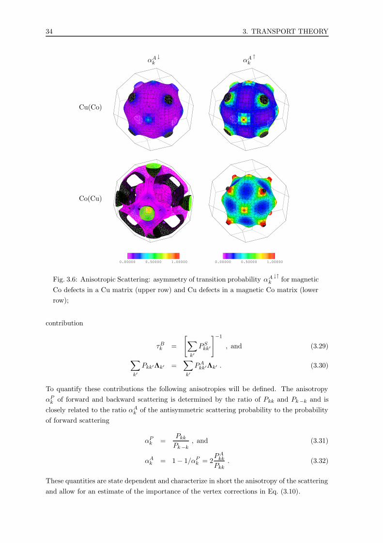
34 3. TRANSPORT THEORY
αAk↓
αAk↑
Cu(Co)
1.00000 5.09902 26.00000
Co(Cu)
0.00000 0.50000 1.00000 0.00000 0.50000 1.00000
Fig. 3.6: Anisotropic Scattering: asymmetry of transition probability αAk↓↑
for magnetic
Co defects in a Cu matrix (upper row) and Cu defects in a magnetic Co matrix (lower
row);
contribution
τBk =
[∑
k′P Skk′
]−1
, and (3.29)
∑
k′Pkk′Λk′ =
∑
k′PAkk′Λk′ . (3.30)
To quantify these contributions the following anisotropies will be defined. The anisotropy
αPk of forward and backward scattering is determined by the ratio of Pkk and Pk−k and is
closely related to the ratio αAk of the antisymmetric scattering probability to the probability
of forward scattering
αPk =PkkPk−k
, and (3.31)
αAk = 1− 1/αPk = 2PAkkPkk
. (3.32)
These quantities are state dependent and characterize in short the anisotropy of the scattering
and allow for an estimate of the importance of the vertex corrections in Eq. (3.10).

3.3. SCATTERING ANISOTROPY 35
The matrix elements of the transition operator are given in the single site approximation
using ASA potentials and the explicit structure of the ∆ n,µL matrix (Eq. (2.50)) by
Tk k = −1
κ
∑
`
(2`+ 1)∣∣∣CµL (k)
∣∣∣2
sin (η` − η`) eı(η`−η`) , and (3.33)
Tk−k = −1
κ
∑
`
(2`+ 1) (−1)`∣∣∣CµL (k)
∣∣∣2
sin (η` − η`) eı(η`−η`) . (3.34)
Here the symmetry of the wave function coefficients under spatial inversion was used
CµL (−k) = (−1)` CµL (k) . (3.35)
So the asymmetry of backward (Pk−k ∝ |Tk−k|2) and forward scattering (Pkk ∝ |Tkk|2) is
determined by the ` = 1 component of the scattering matrix, because terms with ` > 2 are
negligible in transition metal systems, due to the small scattering phase shifts for higher `.
To obtain a large asymmetry αAk , there has to be another than the ` = 1 component present
in the wave function expansion, and the scattering matrix. This means, that the asymmetry
αAk is negligible, if
• only one angular momentum component ` is dominating the scattering matrix (single
channel scattering),
• or the wave function is dominated by one angular momentum (e.g. pure d-state wave
function).
0.00000 0.50000 1.00000
Fig. 3.7: Cu eigenstates: angular momentum character of eigenstates according to
Eq. (2.34), from left to right ` = 0, ` = 1, and ` = 2
These cases are illustrated in Fig. 3.4 for the free electron case. The angle cos (k, k ′) = 1
corresponds to forward scattering and cos (k, k ′) = −1 to backward scattering. Figure 3.4
shows the transition probability Pkk′ for a model system of free electrons with a Fermi level
corresponding to Cu. For the cases of single channel scattering the difference of the phase
shifts η` − η` was chosen to be π2 in the labeled ` channel. The transition probabilities are
symmetric with respect to the angle cos (k,k′) and reflect the symmetry of the Legendre
polynomials PL(cos θ). No asymmetry of Pkk and Pk−k occurs. Furthermore, the scattering

36 3. TRANSPORT THEORY
at a Cu and Co minority potential was simulated. The dominant character of the ` = 2
scattering is evident from the symmetry of the curves and a small asymmetry of Pkk and
Pk−k occurs.
The variation with k of the asymmetry αPk of forward and backward scattering in the Cu
system is shown in Fig. 3.6, and is mainly determined by two ingredients: First, the character
of the Cu host states, and second, the dominance of certain ` components of the scattering
matrix, expressed by η` − η`. The ` character of the states is given in Fig. 3.7. In the neck
regions and in the (100) direction the large asymmetries in the majority channel are caused
by the strong p-character of the eigenstates. Whereas in the (110) direction the dominating
d character suppresses this asymmetry.
3.3.2 Vertex corrections in multilayers
The influence of the vertex corrections in the solution of the Boltzmann equation was
investigated for the Co9Cu7(100) multilayer. The resistances obtained by evaluation of the
vector mean free path by Eq. (3.10) ρ‖ and with Λk in relaxation time approximation ρ‖ are
compared in Fig. 3.8. The largest deviations occur in the minority channel for a Cr defect and
0,81
1,21,41,61,8
min.maj.
ρ ||0 /ρ||
Sc Ti V CrMnFe Co Ni CuZnFig. 3.8: Co9Cu7(100): different defects at Co interface site: ratio
ρ‖ρ‖
of CIP conduc-
tivities calculated with and without vertex corrections, respectively
in the majority channel for the defects from Fe to Zn. The latter is caused by the dominating
sp-scattering since the d-states are fully occupied. The large deviation for the Fe defect is
comparable to the case of Cu defects in a Co host with large asymmetries of the scattering
probability, compare the lower right panel in Fig. 3.6. For pure d scattering or dominating d
character of the states (minority channel) the corrections due to the vertex term are small.
Zhang and Butler proposed a simplified scheme to treat the vertex corrections [117]. The
main purpose was to increase the scattering probabilities to account for the asymmetry of
the scattering, which was determined by the anisotropy of the bulk relaxation times.

3.4. TRANSPORT COEFFICIENTS 37
3.4 Transport coefficients
3.4.1 Residual resistivity
To calculate the residual resistivity, that is the resistivity at zero temperature caused by
the scattering at defects only, the current density is expressed by means of the distribution
function from Eq. (3.5)
j = − eV
∑
k
vkgk . (3.36)
The contribution of the equilibrium occupation function f vanishes. In the limit of zero
temperature and linear response the non-zero contributions of gk are restricted to the Fermi
surface and the current density can be expressed by a Fermi surface integral, using the ansatz
in Eq. (3.7)
j = σE , (3.37)
ji = σijEj , (3.38)
σij =e2
(2π)3
∮
Ek=EF
dS
vkvikΛ
jk , (3.39)
with i and j the Cartesian coordinates and dS a differential Fermi surface element. In non-
magnetic systems a factor 2 has to be included to account for the spin-degeneracy.
In magnetic systems without spin-flip scattering both spin channels contribute to the cur-
rent in parallel applying Motts two-current-model [118]. So, the conductance is splitted in
majority and minority contributions
σ = σ↑ + σ↓ . (3.40)
The resistivity tensor is obtained by inverting the conductance tensor ρ = σ −1, in magnetic
systems for both spin channels likewise. Without spin-orbit coupling and without magnetic
fields the conductivity tensor is diagonal. In the present work metallic layered systems with
a tetragonal symmetry were investigated. In these cases the conductivity tensor contains 2
different entries. For the current in direction perpendicular to the planes of the layers (CPP
geometry), that is parallel to the crystal c-axis, the σCPP , and for the current in direction of
the plane of the layers the σCIP conductivity
σCPP = σzz = σ⊥ = ρ−1⊥ , and
σCIP = σxx = σyy = σ‖ = ρ−1‖ . (3.41)
A spin anisotropy is introduced to account for the individual contributions of the spin channels
in magnetic systems
αi =σii ↑
σii ↓=ρii ↓
ρii ↑. (3.42)

38 3. TRANSPORT THEORY
Applying the relaxation time approximation for the evaluation of the vector mean free path,
the Fermi surface integral for the conductivity contains the tensor of the Fermi velocities
scaled by the state dependent relaxation time
σij =e2
(2π)3
∫
Ek=EF
dS
vkvikv
jkτBk . (3.43)
Averaging over the state dependent relaxation times yields an expression which can be split up
in a Fermi surface integral which contains information about the band structure of the unper-
turbed system only, and a prefactor τ σ which contains the information about the scattering
properties. Despite that the approximation for the scattering properties is rather rough, it
allows for a clear distinction of the influence from the band structure and the scattering at
defects and imperfections.
As discussed by Tsymbal et al. [35] in the present Boltzmann formalism the contribution
of intraband transitions to the conductivity is neglected. Their contributions are small as long
as the imaginary part of the self energy of the states in the system with defects is smaller than
the averaged band separation, as it is shown in section 3.5. For all the systems considered in
this work this criterion is met at least for defect concentrations up to about 1%.
3.4.2 Giant magnetoresistance
The discovery of giant magnetoresistance (GMR) in magnetic multilayer systems [7, 8] ini-
tiated a variety of experimental and theoretical investigations to elucidate the microscopic
origin of the phenomenon. The effect was first discovered in metallic multilayers made up
of magnetic layers separated by non-(ferro)magnetic layers. The effect is closely linked to
the effect of Interlayer Exchange Coupling (IEC) which was discovered some years earlier
by Grunberg at al. [4]. In those samples a magnetic coupling of adjacent magnetic layers
occurs which is mediated by the electrons of the non-magnetic layer. The strength JAF and
sign of the coupling depends on the thickness of the non-magnetic layer and is illustrated in
Fig. 3.9.
d
JAF
∼ sin(2kF d)d2
Fig. 3.9: Interlayer exchange coupling: dependence of the antiferromagnetic coupling
strength JAF in dependence on the interlayer thickness d; in the thickness ranges of
ferromagnetic coupling the coupling strength is hard to obtain in experiment, see [119]

3.4. TRANSPORT COEFFICIENTS 39
Applying an external magnetic field the relative orientation of the magnetization directions
can be changed. That is, in systems without an intrinsic coupling of the magnetic layers the
switching of the magnetic layers can be triggered by their magnetic anisotropy caused by
different layer thicknesses, crystal structures and alloying. During this transition a drastic
change in the electrical resistivity was observed. The first experiments were carried out at
Fe/Cr multilayers and changes up to 50 % were achieved, see Fig. 3.10. To quantify the GMR
Fig. 3.10: Giant magnetoresistance: change of resistance and orientation of the mag-
netization directions in the Fe layers in dependence on the external magnetic field,
experimental reults from [7]
effect the following ratio was introduced
GMR =ρAP − ρP
ρP=
σP
σAP− 1 . (3.44)
This definition is the so-called optimistic one, because it can reach values much larger than 1.
It will be used throughout this work. Some authors prefer to use the pessimistic definition,
which takes in cases of positive GMR (ρAP > ρP ) smaller values, and is given by
GMR′ =ρAP − ρPρAP
= 1− σAP
σP. (3.45)
It was shown by several authors [36, 37, 38, 120] that GMR in magnetic multilayers is strongly
influenced by the electronic structure of the system as a function of the magnetic configura-
tion. That is the difference in Fermi velocities of the multilayers for parallel or antiparallel
alignment of magnetic moments in adjacent magnetic layers that establish GMR by them-
selves. Since this effect is a result of Bragg reflection in ideal multilayers it might be less
important in dirty samples which still have a remarkable GMR amplitude. Consequently,

40 3. TRANSPORT THEORY
spin-dependent scattering [20, 29, 121, 24, 26, 122] is assumed to play a crucial role for
GMR. It could be demonstrated in experiments [123, 124, 125] and theory [94, 126, 127] that
interface scattering is crucial for the size of the effect. The authors presented a systematic
analysis of impurity scattering cross sections as a function of position of the scatterer in the
multilayer and the results will be discussed in section 5.
3.4.3 Conductance of 2-dimensional systems
To describe the electronic structure of metallic slabs with a finite thickness a 2-dimensional
geometry was used. The system is modeled by a prolonged unit cell which is periodically
repeated in two directions, and the third dimension determines the extent of the system in
the direction perpendicular. To describe the surfaces correctly several layers with empty
spheres are added to provide a correct confinement of the valence electrons. The in-plane
conductivity σ‖ in relaxation time approximation (state and spin independent) is given by a
Fermi surface integral over the in-plane component of the Fermi velocity vσk squared [40]
σ =e2
4π2
∑
σ
∫d2kδ(Eσk −EF )
∣∣∣vσk ‖∣∣∣2τσk . (3.46)
The k-integration is performed over the two-dimensional Brillouin zone of the slab. The
Fermi surface reduces to a set of closed lines in the plane perpendicular to the growth di-
rection, see Fig. 4.5. The result of Eq. (3.46) is a slab conductivity per unit cell for a two-
dimensional system. If we consider only one monolayer then we obtain a conductivity per
atom which compares directly to the bulk conductivity. The conductance calculated for a
sample with a channel width W and length L, has the same unit as the specific conductivity
obtained by Eq. (3.46).
The wavefunctions Ψσk (rν + r) of the one-electron eigenstates are normalized to the volume
of the unit cell. Splitting up the real space integral into a sum over the atomic spheres a
site-dependent probability amplitude P σk (ν) of the eigenstate Eσ
k is defined
1 =
∫
unitcelld3r |Ψσ
k(r)|2 (3.47)
=∑
ν
∫
ASAν
d3r |Ψσk(rν + r)|2 =
∑
ν
P σk (ν) . (3.48)
rν are the basis vectors, denoting the different atomic layers, while the real space integration
in Eq. (3.48) is restricted to the atomic sphere (ASA).
To analyze the spatial distribution of the current a local conductivity is introduced by pro-
jecting the conductivity on each atomic layer ν
σσν =e2
4π2τ
∫d2kδ(Eσk −EF )
∣∣∣vσk ‖∣∣∣2P σk (ν) . (3.49)
Thus the total conductivity is just the sum over all the layers N of the slab, and spin directions
σ =∑
σ
N∑
ν=1
σσν . (3.50)

3.5. KUBO VS. BOLTZMANN FORMALISM 41
3.5 Equivalence of Kubo and Boltzmann formalism in the
weak scattering limit
Using the Kubo formalism the conductivity is evaluated fully quantum mechanically by the
current-current correlation function for the ground state [18]. It is a form of the fluctuation-
dissipation theorem, relating a transport coefficient, which characterizes a dissipative process,
to the fluctuations about the equilibrium. It gives the transport coefficient in the linear re-
sponse regime and there are no restrictions concerning the strength of the scattering occurring
in the system. Using the Boltzmann approach one has to assume that the energy bands
are still well defined in the case that impurities are added to the otherwise perfect sample.
This restricts the applicability of the Boltzmann formalism to the case of dilute alloys or
weak scattering, where the mean free path is much longer than the periodicity of the perfect
sample. Conditions for the weak scattering limit will be formulated in terms of scattering
properties and band structure characteristics. In the following the equivalence of both ap-
proaches in the cases of weak scattering and, or low defect concentration will be shown. The
representation in the framework of a Green’s function multiple-scattering formalism will be
used. In a more general context this was shown by Mahan [128].
First, the expression for the conductivity will be derived starting from the Kubo-Greenwood
formula and using the one-particle Green’s function. The Green’s function will be expressed
using the coherent-potential approximation (CPA) as first proposed by Veliciky and others
[105, 106, 129]. Second, using the Green’s function of the coherent medium and the transition
matrices of the single defects the correspondence of the higher order terms in the expansion
to the exact solution of the Boltzmann equation (A.2) will be demonstrated. The criteria
for the applicability of the Boltzmann approach can easily be deduced.
The zero temperature conductivity can be obtained from the current operator by the com-
monly used expression [18, 104, 105]
σij(E) =π
NΩ
⟨Tr J i δ(E −H )J j δ(E −H )
⟩conf
, with
J i = −2ıe∂
∂xi. (3.51)
It can be considered in terms of nonlocal conductivities connecting the external field in
direction i at one site to the induced current in direction j at another site. N denotes the
number of atoms in the sample, Ω is the volume per atom. For systems with a basis it is
replaced by the normalization volume V of the wave function introduced in section 2.4. We
consider a sample containing defects α at random positions with relative concentrations cα.
The defect concentrations cα give the number of defects per normalization volume. H is
the Hamilton operator of one realization of the random potential. The large brackets 〈〉confdenote the configurational average. xi is a Cartesian coordinate of the real space vector
r = (x1, x2, x3). Using the Green’s function the δ-functions can be replaced by
δ(E −H ) = − 1
πImG (E+) , with
= − 1
2πı
[G (E+)− G (E−)
], with E± = E ± ı0 , (3.52)

42 3. TRANSPORT THEORY
and the expression from equation (3.51) splits into 4 parts
σij(E) =1
4
(σij++ + σij−− − σij−+ − σij+−) , with (3.53)
σij±± = − 1
πNΩ
⟨Tr J iG (E±)J jG (E±)
⟩conf
.
To evaluate the average over the Green’s function G (E±) the CPA is used. Starting point
is the ideal system which can be periodic in certain directions and is characterized by the
Green’s function G (E) =(E − H
)−1. ∆V is the perturbation potential for one realization
of the defect distribution in the sample, and it defines the Green’s function
G (E) =(E − H −∆V
)−1. (3.54)
A coherent medium is introduced by averaging the Green’s function over all defect configu-
rations
g(E) = 〈G 〉conf =(E − H − Γ
)−1. (3.55)
Γ is the self energy which describes the shift and broadening of the eigenstates due to the
scattering at the defects, and is complex in general. These Green’s functions are connected
by a Dyson equation
G = g + g (∆V − Γ)G= g + gT g . (3.56)
The average of the scattering operator T vanishes due to the CPA condition in Eq. (3.55)
〈(∆V − Γ)G 〉conf = 〈T 〉conf = 0 . (3.57)
The single defect scattering matrix T α(E) characterizes the transition from the coherent
medium to a system with one defect of type α at a certain position
Tα(E) = ∆tα(E) (1− g(E) ∆tα(E))−1 , with ∆tα(E) = tα(E)− tc(E) . (3.58)
tc is the single site scattering matrix of the coherent medium. The matrix elements of the
current operator using the local angular momentum basis
〈 r ||α,L,E 〉 = Rα` (r, E)YL(r) = RαL(r, E) (3.59)
at a position occupied by a defect of type α are
J i αLL′(E1, E2) = −2ıe
∫d3rRαL(r, E1)
∂
∂xiRαL′(r, E2) . (3.60)
Averaged current operators are defined by
J i=∑
α
cαJ i α . (3.61)
Neglecting some correlations in the current-current correlation function the expression for
σij−+ and σij+− can be further simplified. It can be shown that the contribution of σ ij++

3.5. KUBO VS. BOLTZMANN FORMALISM 43
and σij−− is negligible due to the occurrence of k-space resonances in the former ones [106].
Furthermore the contribution of terms including on-site elements of the Green’s function only
will be omitted for the same reason. Defining functions
χL1L2;L3L4(E+, E−) =∑
n
g0nL2L3
(E+)g0nL4L1
(E−) , and (3.62)
WL1L2;L3L4(E+, E−) =∑
α
cαTαL1L4
(E+)TαL3L2(E−) , (3.63)
the following compact solution for σij+− is obtained
σij+− = − 1
πNΩ
∑
L1L2;L3L4
JiL1L2
(E−, E+)[(1− χW )−1 χ
]L1L2;L3L4
JjL3L4
(E+, E−)
= − 1
πNΩ
∑
L1L2;L3L4
JiL1L2
(E−, E+)
∞∑
γ=1
[(χW )γ−1 χ
]L1L2;L3L4
JjL3L4
(E+, E−)
= σij+−1 + σij+−
2 + . . . . (3.64)
Replacing (1− χW )−1 by the unity matrix the vertex corrections are neglected
σij+−1 = − 1
πNΩ
∑
L1L2;L3L4
JiL1L2
(E−, E+) [χ ]L1L2;L3L4JjL3L4
(E+, E−) , (3.65)
and the second term in the expansion is given by
σij+−2 = − 1
πNΩ
∑
L1L2;L3L4
JiL1L2
(E−, E+) [χWχ]L1L2;L3L4JjL3L4
(E+, E−) . (3.66)
In the following it will be demonstrated that the result neglecting the vertex corrections
σijNV C = −14
(σij+−
1 + σij−+1
)will recover the result of the Boltzmann equation without
vertex corrections in the case of well defined bands of the coherent medium. It corresponds
to the first term in the expansion of the exact solution of the Boltzmann equation (A.2).
Furthermore, both expansions are equivalent, as will be demonstrated for the second term of
σij+− and the expansion of Λk.
Due to the translational invariance of the coherent medium the real space sum in Eq. (3.65) is
evaluated by a Fourier transformation. Using the spectral expansion of the Green’s function
and assuming poles Ek0 = E+ in k-space the Green’s function of the coherent medium can
be expanded in the vicinity of these poles as
g(k, E+) =∑
k0
|k0 〉〈k0 |vk0 (k0 − k)
, with vk0 =∂Ek
∂k
∣∣∣∣k=k0
. (3.67)
The poles k0 are in general complex, even if the energy E is real. Exploiting the locality of
the current operator 〈k |J i|k′ 〉 = evikδkk′ one obtains for the conductivity contribution
σij+−1 = − e2
πΩΩBZ
∫d3k
∑
Ek0=E+
vik0vjk0
vk0 (k− k0) vk0 (k− k∗0), (3.68)

44 3. TRANSPORT THEORY
with ΩBZ the volume of the Brillouin zone. The integrand is determined by the poles δ(k−Re k0). Splitting the integration d3k = dkdk in direction parallel and perpendicular to vk0
and expanding k = Re k0 + kvk0 + k⊥ one obtains
σij+−1 = − e2
πΩΩBZ
∑
Ek0=E+
∫dkdk
vik0vjk0
vk0vk0
1
k2 + (vk0Im k0)2
. (3.69)
Evaluating the integral∫
dk, introducing the Boltzmann life time
τBk0=
1
2ImERek0
=1
2 |vk0Im k0|, (3.70)
replacing k0 by k, and using ΩΩBZ = (2π)3 one obtains
σij+−1 = − 2e2
(2π)3
∫
Ek=E+
dS
vkvikv
jkτ
Bk . (3.71)
From that point it is easily to recognize that σijNV C = −14
(σij+−
1 + σij−+1
)from Eq. (3.53)
is identical to the conductivity tensor obtained by evaluating the Boltzmann equation in
the relaxation time approximation in Eq. (3.43).
The second term in the expansion of σij+− in Eq. (3.64) is
σij+−2 = − N
πΩ
∑
n,m,αL1...L8
JiL1L2
(E−, E+)g0nL2L3
(E+)TαL1L4(E+)gn n+m
L4L5(E+)∗
JjL5L6
(E+, E−)gn+mmL6L7
(E−)TαL7L8(E−)gm0
L8L1(E−) .
(3.72)
The average over the sites n and m can be restricted to the configurations where both sites
are occupied by the same type of defect. The average over the other configurations vanishes
due to the CPA condition in Eq. (3.55). Introducing the matrix elements of the single defect
scattering matrices
Tαkk′(E+) = 〈 k |T α(E+)| k′ 〉 = 〈 k′ |T α(E−)| k 〉∗ . (3.73)
one obtains
σij+−2 = − e2N
πΩΩ2BZ
∑
Ek0=Ek1
=E+,α
∫d3kd3k′
vik0Tαk0k1
vjk1Tα ∗k0k1
cαN
vk0 (k− k0) vk1 (k′ − k1) vk0 (k− k∗0) vk1 (k′ − k∗1).
(3.74)
Evaluating the k-space integral similar to Eq. (3.68), and introducing the relaxation times
τBk one obtains
σij+−2 = − 4πe2N
(2π)3 ΩBZ
∫
Ek=E+
∫
Ek′=E+
dS
vk
dS
vk′
∑
α
cαN |Tαkk′ |2 vikvjk′τBk τBk′ , (3.75)

3.6. FUCHS-SONDHEIMER TRANSPORT THEORY 45
and using the expression for the microscopic transition probability from Eq. (3.15) this can
be transformed to
σij+−2 = − 2e2V
(2π)6
∫
Ek=E+
∫
Ek′=E+
dS
vk
dS
vk′vikv
jk′τ
Bk τ
Bk′Pkk′ . (3.76)
This corresponds to the second term in the expansion of [1− τP ] ∗ −1 in equation (A.2). As
can be seen easily both expansions are equivalent term by term in the limit of well defined
bands in the coherent medium. This is the case for low concentrations and is even valid in
the case of arbitrary concentration but weak scattering, as was shown by Butler [106].
The criterion of well-defined bands should be expressed for multilayers in terms of the mul-
tilayer periodicity in growth direction c and the mean free path Λ. The averaged band
separation ∆E is given by the band width EB, the number of atomic layers N forming one
multilayer period, and the number ne of electrons with given angular momentum (1 and 5 for
s and d electrons respectively). The averaged Fermi velocity is estimated by the band width
and a typical Brillouin zone diameter πa , with a the in-plane lattice constant
∆E =EBneN
, , and
vF =EBπa
=Λ
τB. (3.77)
The imaginary part of the self energy Γ′′ is related to the Boltzmann relaxation time by
Eq. (3.70) Γ′′ = 1/2τB . The criterion for well-defined bands is, that the imaginary parts of
the coherent medium energy bands are smaller than the averaged band separation, and can
be expressed by
∆E > 2Γ′′ , (3.78)
which can be transformed by use of (3.11), (3.70), and (3.77) to obtain
Λ >neπc . (3.79)
This criterion is met by all considered systems in this work for defect concentrations at
least up to 1%. This means, for defect concentrations up to this value the solution of the
Boltzmann equation is equivalent to the Kubo-Greenwood formalism and describes the
transport properties correctly.
3.6 Fuchs-Sondheimer transport theory
In the derivation of the Boltzmann theory in section 3.1 a homogeneous system on the
length scale of the mean free path (MFP) was assumed and the diffusion term in Eq. (3.1) was
neglected. Based on the ideas of Fuchs and Sondheimer a transport theory was developed
which assumes a distribution function, nonuniform in space, accounting for inhomogeneities,
like surfaces and interfaces.

46 3. TRANSPORT THEORY
Let us consider a thin metallic layer perpendicular to the z-axis: The master equation for the
deviation from the equilibrium distribution function using the relaxation time approximation
is written as
∂gk(z)
∂z+ k
∂fk(z)
∂k+gk(z)
τk= 0 . (3.80)
Introducing a position dependent vector MFP similar to Eq. (3.7) one obtains a differential
equation
τkvzk
∂
∂zΛk(z) + Λk(z) = τkvk = Λk , (3.81)
which contains the vector MFP of the bulk material Λk. It can be solved in general form
Λk(z) = Λk + λke− zτkvz
k . (3.82)
Assuming for λk = FkΛk the same direction as Λk the general solution can be written as
Λk(z) = Λk
(1 + Fke
− zτkvz
k
). (3.83)
The arbitrary real function Fk has to be determined by appropriate boundary conditions at
the film surfaces. Fuchs introduced the following boundary conditions for the distribution
function using a parameter P to characterize the fraction of specular reflected electrons. The
fraction (1 − P ) is scattered diffusive. To account for the incoming and outgoing waves at
the surface the states are labeled by their Fermi velocity in z-direction by k+ with vzk > 0
and k− with vzk < 0 assuming a common in-plane wave vector k‖. For the surface at z = −aand z = a the following boundary conditions apply
gk+(−a) = Pgk−(−a) ,
gk−(a) = Pgk+(a) . (3.84)
For magnetic systems all properties are spin-dependent. The resulting system of linear equa-
tions for the functions Fk can be solved easily and the film conductivity is calculated as
described in section 3.4.
For film thicknesses d large in comparison to the MFP the specific conductivity normalized
to the volume tends asymptotically to the bulk value σ
σ
σ=ρ
ρ= 1 +
3(1− P )Λ
8d(d >> Λ) , (3.85)
with Λ an average value over the states at the Fermi level. The additional resistivity contri-
bution is proportional to the diffusive surface scattering (1 − P ). For small film thicknesses
where the assumption of position dependent distribution functions is quite questionable the
layer conductivity tends to zero as
σ
σ=d
Λlog(
Λ/d)
(d << Λ) . (3.86)
This is illustrated in Fig. 3.11, left panel.
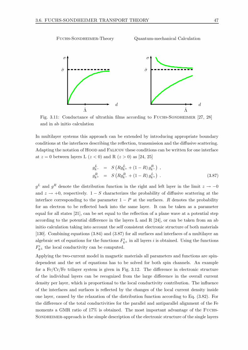
3.6. FUCHS-SONDHEIMER TRANSPORT THEORY 47
Fuchs-Sondheimer-Theory Quantum-mechanical Calculation
d
Λ
σ
σ
d
Λ
σ
σ
Fig. 3.11: Conductance of ultrathin films according to Fuchs-Sondheimer [27, 28]
and in ab initio calculation
In multilayer systems this approach can be extended by introducing appropriate boundary
conditions at the interfaces describing the reflection, transmission and the diffusive scattering.
Adapting the notation of Hood and Falicov these conditions can be written for one interface
at z = 0 between layers L (z < 0) and R (z > 0) as [24, 25]
gLk− = S(RgLk+ + (1−R) gRk−
),
gRk+ = S(RgRk− + (1−R) gLk+
). (3.87)
gL and gR denote the distribution function in the right and left layer in the limit z → −0
and z → +0, respectively. 1 − S characterizes the probability of diffusive scattering at the
interface corresponding to the parameter 1 − P at the surfaces. R denotes the probability
for an electron to be reflected back into the same layer. It can be taken as a parameter
equal for all states [21], can be set equal to the reflection of a plane wave at a potential step
according to the potential difference in the layers L and R [24], or can be taken from an ab
initio calculation taking into account the self consistent electronic structure of both materials
[130]. Combining equations (3.84) and (3.87) for all surfaces and interfaces of a multilayer an
algebraic set of equations for the functions F ik± in all layers i is obtained. Using the functions
F ik± the local conductivity can be computed.
Applying the two-current model in magnetic materials all parameters and functions are spin-
dependent and the set of equations has to be solved for both spin channels. An example
for a Fe/Cr/Fe trilayer system is given in Fig. 3.12. The difference in electronic structure
of the individual layers can be recognized from the large difference in the overall current
density per layer, which is proportional to the local conductivity contribution. The influence
of the interfaces and surfaces is reflected by the changes of the local current density inside
one layer, caused by the relaxation of the distribution function according to Eq. (3.82). For
the difference of the total conductivities for the parallel and antiparallel alignment of the Fe
moments a GMR ratio of 17% is obtained. The most important advantage of the Fuchs-
Sondheimer-approach is the simple description of the electronic structure of the single layers

48 3. TRANSPORT THEORY
by the bulk properties. This causes limitations of the method, because quantum-size effects
due to small layer thicknesses and their influence on the scattering properties can not be
included. This approach was successfully applied to GMR systems by many authors [20, 21,
22, 23, 24, 25].
Fig. 3.12: In-plane current density over the thickness of an Fe/Cr/Fe trilayer, solid and
dashed-dotted line for the minority and majority contribution in the parallel configu-
ration and the dotted and long dashed-dotted line for the antiparallel configuration,
respectively; parameter S↑ = 1, S↓ = 0, and P ↑,↓ = 0.5, from [24].
3.7 Landauer formalism
For mesoscopic systems where the system size plays a crucial role for transport properties
the Landauer-Buttiker theory is an established method [131, 132, 133, 134, 135]. The
considered device contains a scattering region which is connected to electron reservoirs by
ideal leads which feed the current into and take it out. The measuring geometry determines
the assumption to be made in the applying the formalism. A two-terminal device is charac-
terized by two reservoirs and current as well as voltage are measured at the same leads. It is
assumed that the transmission matrix elements are small compared to unity, which describes
a tunnel junction. In the case of zero temperature and within linear response the Landauer
conductance becomes
C =e2
h
∑
kL,kREkL=EkR=EF
TkLkR , (3.88)

3.7. LANDAUER FORMALISM 49
with TkLkR the quantum mechanical probability for a state kL incident from the left reservoir
to be transmitted into state kR of the right hand side reservoir. kL and kR are the quantum
numbers of the eigenstates in the left and right hand side electrode, respectively, which are
normalized to carry a unit current (〈 k |J z | k 〉 = 1). This formula was empirically derived for
one-dimensional systems. Fisher and Lee have later shown that Eq. (3.88) can be extended
to systems of higher dimensions using the transmission matrix t from either the left or the
right reservoir [136]
C =e2
hTr(t+t). (3.89)
For planar junctions with an in-plane periodicity and magnetic electrodes kL,R is a shorthand
notation for (k‖, ν, σ), the in-plane wave vector k‖, band index ν, and spin σ.
For ballistic transport, that is no scattering occurs in the sample, all states are not scattered
at all and the transmission matrix is the unity matrix with the dimension equal to the number
of eigenstates in the reservoirs. By this assumption the sum in Eq. (3.88) can be transformed
in a Fermi-surface integral [137]
C =e2
h
1
2
∑
Ek=EF
|nvk| , (3.90)
with n the unit vector of the current direction and vk the Fermi velocity of the Bloch eigen-
states of the system. Transforming the k sum into an integral one obtains the specific conduc-
tivity normalized to the junction area A as a Fermi surface integral weighted by the absolute
value of the Fermi velocity in current direction
C
A=e2
h
1
4π2
1
2
∮
Ek=EF
dS
vknvk . (3.91)
The similarities to the transport coefficients in the diffusive regime in Eq. (3.43) are obvious.
The conductance in Eq. (3.91) describes the transport between two identical electrodes con-
nected by a narrow region (point contact) of the same electronic structure. The transport
is determined by the ballistic motion of electrons if the diameter of the contact is small in
comparison to the MFP. Even though the electrons are not scattered, the conductance is fi-
nite due to the finite diameter of the contact and the finite number of transverse eigenmodes.
This is equivalent to the Sharvin contact resistance [138].
This idealized situation can be achieved in GMR experiments at least in the current-per-
pendicular-plane (CPP) configuration, if the total multilayer stack thickness is smaller than
the MFP. This formalism was applied by several authors to elucidate the intrinsic, from the
coherent electronic structure, origins of CPP-GMR [38, 139].


Chapter 4
Transport in ultrathin films
4.1 Introduction
The understanding of the size-dependent conductivity in thin-film multilayers is still an open
question. The conductivity of various magnetic/non-magnetic multilayer systems [140, 141,
142, 143, 144, 145] has been measured as a function of the thickness of the deposited layer.
These electrical measurements were made simultaneously by in-situ conductance monitoring,
and the experimental data show characteristic features for all investigated multilayers. First
of all, the conductance increases with increasing multilayer thickness. Second, the slope of
the conductance increase is different for the different metal layers, due to the corresponding
residual resistivity of the metals. Third, there is a characteristic drop in the total conductance
as soon as the magnetic layer is added on top of the non-magnetic layer. This behavior is
quite general and was originally related to additional scattering in the interface region due
to intermixing and disorder.
Several models have been developed to understand the origin of this behavior. Most of them
have assumed free-electron behavior within the constituent layers [146, 147, 148], extending
the Fuchs-Sondheimer approach [27, 28]. Disorder at the interface was introduced. A
quantum mechanical description including surface scattering was presented by Fishman and
Calecki [33, 149] and by Trivedi and Ashcroft [150]. A more realistic description of
the multilayer was based on a tight binding model including disorder at the interface [140].
Ab initio electronic structure calculations of magnetic multilayers have been performed by
several groups [37, 38, 44, 46, 94]. It was shown that the electronic structure of the multilayer
plays a very important role for the understanding of the transport properties and giant
magnetoresistance [7, 8]. None of the calculations were performed for the in-situ conductance-
monitoring considering the incremental conductance contributed by each atomic layer. The
aim of these investigations was the understanding of the size dependence and the evolution
of the Co/Cu multilayer conductivity during the growth, starting from ab-initio electronic
structure calculations.
To simulate the in situ conductance-monitoring of the Co/Cu multilayer during growth we
model the system by the following assumptions. We consider a monolayer growth along the
51

52 4. TRANSPORT IN ULTRATHIN FILMS
(001) direction. Co and Cu are assumed to occupy an ideal fcc lattice with a lattice constant
of 6.76 a.u., without any lattice mismatch or distortion at the interfaces and surfaces, while
no intermixing at the interfaces is allowed.
In the experimental setup an insulator or semiconductor buffer or target material is used,
which is simulated by vacuum in our calculation. That means a free standing slab with
2D periodicity in the plane is considered. For the calculations we started from a Cu slab
of 2 monolayers (ML) thickness. Cu was added layer by layer until a thickness of 5 ML
was reached which corresponds to about 9A. We continued by adding Co up to the same
thickness. Then the cycle was repeated. The short-hand notation for the considered systems
is Cun1/Con2/Cun3 ... denoting the individual layer thicknesses in monolayers starting from
the bottom Cu layer . Every multilayer corresponds to an experimental film after deposition of
a complete ideally flat atomic layer. The electronic structure was determined self-consistently
for each system under consideration. Concerning the magnetic configuration of the multilayer
slabs we assumed parallel alignment of the Co layer magnetization which is energetically
preferred in Co/Cu multilayers [151] with 5 ML Cu thickness.
4.2 Ultrathin Cu films
Growth
0 1 2 3 4 50
5
10
15
20
25 σσ/Nlinear regression
σ
N (Cu monolayer)
Fig. 4.1: Film conductivity (dots) and conductivity per atom (crosses) as a function of
Cu layer thickness in arbitrary units. [152]
Following the ideas of Fuchs and Sondheimer [27, 28] the conductivity of a simple metallic

4.3. CONDUCTANCE ANOMALY DURING GROWTH 53
film goes to zero with decreasing film thickness d, since in the limit of thin films: σ ∼κ ln(1/κ), where κ = d/Λ, and Λ denotes the mean free path. Considering no diffusive surface
scattering we obtain the bulk conductivity. In a realistic quantum mechanical calculation
where full band structure effects are present the situation is more complicated. Depending on
the electronic structure of the material a decrease or increase can be expected, as illustrated
in Fig. 3.11, right panel. In Fig. 4.1 we present the calculated conductivity of ultrathin
Cu slabs with thicknesses varying from two to five monolayers. The electronic structure was
determined self-consistently for every system and the constant relaxation time approximation
according to Eq. (3.12) was applied. These are specific conductivities for the 2D geometry.
Normalized to the thickness of the layers these values can be compared with the usual bulk
conductivity (compare section 3.4.3). The total slab conductivity increases almost linearly
with the number of Cu monolayers. The conductivity per atom tends to saturate to a constant
value after 4-5 ML. It is obvious that our calculated conductivity does not extrapolate to
zero as predicted by the Sondheimer model. This is a direct consequence of the quantum
mechanical treatment of the surface. In the Sondheimer model the surface is included by the
boundary condition for the classical electron distribution function. In the present calculation
the full quantum mechanical Hamiltonian for the surface is used. As a result new types of
eigenstates, like surface states, could appear which are not included in the Sondheimer model.
Due to the formation of surface states with a high in-plane group velocity the conductivity
per atom increases for very thin Cu slabs, see Fig. 4.1. It has to be mentioned that the
constant relaxation time that is used for all states at the Fermi level might be inaccurate to
obtain quantitative information.
4.3 Conductance anomaly during growth
The calculated conductivity of the Cu/Co slabs is shown in Fig. 4.3, together with the DOS
at the Fermi level. With our calculation we are able to reproduce the experimentally observed
behavior shown in Fig. 4.2. Our results show an increase with increasing slab thickness, while
there is a drop in the slab conductivity of about 20% when the first Co monolayer is deposited
on Cu. By adding more Co layers σ increases further, and we observe no significant effect
when we start depositing Cu again. A drop is again seen when we repeat the Co deposition on
top of Cu. The spin decomposition shows that for majority electrons we have a monotonous
increase in σ, while the peculiar, non-Ohmic conductivity variation stems from the minority
electrons. Here we point out that no specific surface scattering mechanism is included in the
calculation. Moreover, a constant spin-independent relaxation time was assumed, and the
difference in the spin channels comes solely from the contrast of electronic structure in the
two spin channels while differences in scattering which would require an anisotropic τ are
ignored in this approximation.
It is interesting to compare the evolution of the conductivity with the changes of the slab
DOS at the Fermi level, shown in Fig. 4.3. For the majority channel we observe a linear
increase with thickness since the local DOS at EF at the Co and Cu sites is very similar

54 4. TRANSPORT IN ULTRATHIN FILMS
⇒ ⇒ ⇒
of Cr~100 Å!/Au~3000 Å! through a shadow mask; substratesfor the pad deposition are 4-in. thermally oxidized Si waferscoated with 400 Å NiO. The Si wafer is cleaved into cou-pons after pad deposition to avoid sputtering onto and con-duction through the sample sides. Typical point-to-point re-sistances of the bare Si/SiO2 /NiO~/Au-contact! substrate,measured in situ immediately prior to spin-valve deposition,were 1 MV, with 0.5 MV measured in the four-wire geom-etry. Measurement and deposition take place at ambient tem-perature ~300 K!. A thermocouple located beneath thesample during similar depositions has shown very little tem-perature rise due to sputtering, with an increase of ,5 °Crecorded over 30 min continuous sputtering.
For this study, a series of NiO/Co~20!/Cu(t)/Co(50 Å)spin-valve structures in Cu thickness, t57.8, 11.0, 15.5, 23.3Å, was deposited and conductances measured in situ. To de-termine the periodicity of features observed, aNiO/Co~20!/@Cu~20!/Co(10 Å)]9 multilayer was measuredin comparison. All layers were formed by ion-beam sputter-ing in UHV with a base pressure of 231029 torr, primarybeam energy of 300 V, working Xe pressure of 431024 torr, and beam current of 5.060.1 mA. The NiOsubstrate was ion cleaned (Vbeam5300 V, PAr5431024 torr,45-s duration! in vacuum immediately prior to deposition.Thicknesses were controlled by deposition time, calibratedby x-ray reflectivity measurements of layer thickness. Aquartz microbalance has been used in some cases as second-ary confirmation of deposition rate. No magnetic field hasbeen applied and no exchange anisotropy introduced duringdeposition.
We have found in previous TEM investigation of ‘‘bot-tom’’ NiO-biased spin valves17 that the deposited layers donot display any net preferred crystal orientation. The pre-dominant growth mode of NiFe/Co/Cu/Co/NiFe on NiO inour system is such that there is local cube-on-cube epitaxybetween randomly oriented fcc NiO grains and columnargrains formed by the NiFe/Co/Cu/Co/NiFe layers. We as-sume here that the bottom NiFe layer does not affect theepitaxy strongly, and that NiO/Co/Cu/Co exhibits similarcrystalline ordering; this has been found to be the case in aHR-xTEM investigation of dc-magnetron sputtered NiO/Co/Cu/Co spin valves by Chopra et al.18
III. EXPERIMENTAL RESULTS
The full thickness-dependent conductivity data forNiO/Co~20!/Cu(t)/Co(50 Å) trilayers, t57.8, 11.0, 15.5,23.3 Å is presented in Fig. 1. Total film conductance mea-sured in situ is plotted vs total layer thickness; the interfacepositions ~Co on Cu, Cu on Co! are indicated by arrows. ForCo on NiO, the onset of normal metallic film conductance isfound at ;6 Å, approximately 3–4 ML coverage. The slopeof the thickness-dependent conductance G(t) increasesgradually and approaches a more linear behavior up to 20 Å.This behavior is consistent with the formation of a high den-sity of defects in the first several monolayers, causing ahigher bulk layer resistivity, after which the layer quality isimproved and lower layer resistivities are attained.
More striking features in conductance are observed at theinterfaces. For Cu on NiO/Co~20 Å!, a strong positive cur-vature is present in G(tCu): additional Cu layers contribute
relatively little to the film conductance for low coverage,with progressively greater incremental contributions atgreater thickness. We point out that the curvature in this plotis everywhere positive, with no kinks in the thickness-dependent conductance present. The incremental contribu-tions to conductance are plotted in more detail in Fig. 2;these are plotted in their inverse units ~resistivity! for easiercomparison with tabulated values. We define the incrementalresistivity as
r~ t !5S ]G~ t !]t D
21
.
The incremental resistivity may be identified with the bulkresistivity for the added layer only in the case where other
FIG. 1. Experimental film conductance G(t tot) measured in situduring deposition of NiO/Co~20!/Cu~tCu!/Co(40 Å) trilayers. Theposition of the interfaces ~starting points for deposition of Cu andCo! is marked for samples A – D . tCu57.8 Å ~A!, 11.0 Å ~B!,15.5 Å ~C!, 23.3 Å ~D!. Note the strong deviations from linearity inthe vicinity of the interfaces.
FIG. 2. Experimental incremental resistivity r(t) for sample D.Note that the rapid decrease in effective resistivity with increasingCu layer thickness is featureless. Saturation resistivities of 6 mV cmfor Cu and 16 mV cm for Co are estimated.
PRB 61 1331ELECTRONIC SCATTERING FROM Co/Cu . . .
Fig. 4.2: Experimental result of in-situ conductance during Cu/Co growth [140]
for the majority channel and corresponds to the free electron like states above the filled 3d
bands. The behavior of the minority DOS reflects the difference in the electronic structure
of the two materials. The DOS is much larger at the Co sites in comparison to Cu, this
causes the strong increase of the total DOS during the Co growth. The local DOS at the
Co surface or at a Co/Cu interface is enhanced in comparison to the bulk Co, and the total
DOS is strongly increased by adding the first two Co layers. Moreover, quantum confinement
effects are fully included in our calculation and cause the reduced increase when depositing
the third Co layer, and the small drop when the single Cu layer terminates the slab.
Let us now concentrate on the drop of the conductivity when adding one monolayer Co on the
Cu film. This behavior is accompanied by a strong increase in the total DOS since the Fermi
level crosses the Co minority band. The spin projected conductivities demonstrate that the
drop occurs in the minority channel. By means of an averaged spin-dependent Fermi velocity
vσ
vσ =
[∫d2kδ(Eσk −EF )vσk ‖
2/nσ(EF )
] 12
, (4.1)
one can rewrite Eq. (3.46) into
σ =e2
4π2τ∑
σ
nσ(EF ) vσ 2 . (4.2)
nσ(EF ) =∫
d2kδ(Eσk − EF ) is the total DOS at Fermi level. The expression in Eq. (4.2) is
useful to understand the microscopic origin of the conductivity drop. Following Eq. (4.2) the

4.3. CONDUCTANCE ANOMALY DURING GROWTH 55
2 3 4 5 51 52 53 54 55 551 552 553 554 555 ..51 ..52 ..530
10
20
30
40
MinMajΣ
0
50
100
150
200 DOS
Conductivity[arb.units]
[1/Ry]
Cu CuCo Co
Fig. 4.3: Evolution of total and spin projected DOS [states/Ry] at EF and total and
spin projected conductivity [arbitrary units] during Co/Cu multilayer growth. [152]
reduction of the conductivity is caused by a strong reduction of the averaged Fermi velocity
in the minority channel since the DOS is strongly increasing. For the majority band we have
a linear increase and no difference is seen when going from Cu to Co and vice versa since the
Co d states are below the Fermi level. To elucidate this Fermi velocity reduction the local
conductivity of the minority channel Eq. (3.49) is shown in Fig. 4.4, for nearly all slabs under
consideration. For the pure Cu slabs all Cu layers contribute equally to the conductivity, and
we observe only a small reduction at the surface layers. The situation changes drastically
when we consider a single monolayer of Co on the Cu slab. As we can see from Fig. 4.4
(third panel from bottom), the major contribution in the conductivity comes from the Co
layers, the Cu contributions however, are significantly decreased by almost a factor of four in
comparison to the Cu slabs without Co coverage. According to Eq. (4.2), this corresponds to
a reduction of the effective Fermi velocity by a factor of two and the total slab conductivity
is decreased, see Fig. 4.3. This reduction of the Fermi velocity stems from a drastic change of
the Fermi surface topology when adding a single Co layer on top of Cu as shown in Fig. 4.5.
The deposition of a simple Co layer destroys the free electron like Cu-slab Fermi surface in
the minority band while the majority Fermi surface is kept intact. As a result we end up

56 4. TRANSPORT IN ULTRATHIN FILMS
Cu Cu Co Co Cu CuVac0.00.51.01.52.0
Cu Cu Co Co Cu Cu Co0.00.51.01.52.0
Cu Cu Co Co Cu CuVac0.00.51.01.52.0
Cu Cu Co Co Cu CuVac0.00.51.01.52.0
Cu Cu Co Co Cu CuVac0.00.51.01.52.0
Cu Cu Co Co CuVac0.00.51.01.52.0
Cu Cu Co CoVac0.00.51.01.52.0
Cu CuVac0.00.51.01.52.0
Cu CuVac0.00.51.01.52.0
Cu Cu CoVac0.00.51.01.52.0
Cu Cu Co CoVac0.00.51.01.52.0
Fig. 4.4: Evolution of the local conductivity of the minority channel calculated by
Eq. (3.49) [arbitrary units] during film growth [152]
with a complicated minority Fermi surface dominated by Co d states of low velocity. Despite
the low velocity of the Co d-states, Co layers have a high conductivity σ because of the high
DOS. Moreover, Co surface and interface states produce a further enhancement.
The constant reduction of the Cu contribution implies also the experimentally found pro-
portionality of the conductivity drop in dependence on the Cu layer thickness [140]. The
conducting states have a large probability amplitude at the surface, which would give an am-
plification of the conductivity drop due to the enhanced scattering cross section [153]. This
is in line with numerical results of Tsymbal [140] assuming a larger potential disorder at the
Co/Cu interface in comparison to the bulk materials.
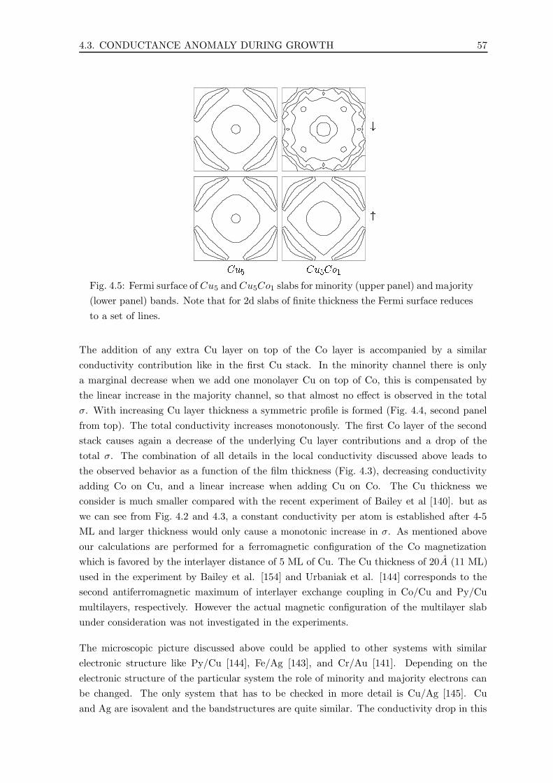
4.3. CONDUCTANCE ANOMALY DURING GROWTH 57
Fig. 4.5: Fermi surface of Cu5 andCu5Co1 slabs for minority (upper panel) and majority
(lower panel) bands. Note that for 2d slabs of finite thickness the Fermi surface reduces
to a set of lines.
The addition of any extra Cu layer on top of the Co layer is accompanied by a similar
conductivity contribution like in the first Cu stack. In the minority channel there is only
a marginal decrease when we add one monolayer Cu on top of Co, this is compensated by
the linear increase in the majority channel, so that almost no effect is observed in the total
σ. With increasing Cu layer thickness a symmetric profile is formed (Fig. 4.4, second panel
from top). The total conductivity increases monotonously. The first Co layer of the second
stack causes again a decrease of the underlying Cu layer contributions and a drop of the
total σ. The combination of all details in the local conductivity discussed above leads to
the observed behavior as a function of the film thickness (Fig. 4.3), decreasing conductivity
adding Co on Cu, and a linear increase when adding Cu on Co. The Cu thickness we
consider is much smaller compared with the recent experiment of Bailey et al [140]. but as
we can see from Fig. 4.2 and 4.3, a constant conductivity per atom is established after 4-5
ML and larger thickness would only cause a monotonic increase in σ. As mentioned above
our calculations are performed for a ferromagnetic configuration of the Co magnetization
which is favored by the interlayer distance of 5 ML of Cu. The Cu thickness of 20A (11 ML)
used in the experiment by Bailey et al. [154] and Urbaniak et al. [144] corresponds to the
second antiferromagnetic maximum of interlayer exchange coupling in Co/Cu and Py/Cu
multilayers, respectively. However the actual magnetic configuration of the multilayer slab
under consideration was not investigated in the experiments.
The microscopic picture discussed above could be applied to other systems with similar
electronic structure like Py/Cu [144], Fe/Ag [143], and Cr/Au [141]. Depending on the
electronic structure of the particular system the role of minority and majority electrons can
be changed. The only system that has to be checked in more detail is Cu/Ag [145]. Cu
and Ag are isovalent and the bandstructures are quite similar. The conductivity drop in this

58 4. TRANSPORT IN ULTRATHIN FILMS
system might be related to alloying only.
Based on ab-initio calculations of the conductivity of Cu/Co slabs we have shown that the
variation during growth can be explained by the changes of the electronic structure as a
function of the film thickness. In general the total conductivity of a multilayer slab increases
with increasing thickness. A pronounced conductivity drop is obtained when the first Co
layer is deposited on top of the Cu. Due to interaction of the Co d-electrons with the Cu
s-electrons the character of the minority Fermi surface is changed from sp to d-like. As a
consequence the local conductivity contributions of the Cu layers are reduced. Since the total
DOS at the Fermi level is increasing during film growth the effect is related to reduced Fermi
velocities. The microscopic picture can be generalized to any multilayer consisting of noble
and transition metal layers. This effect is not in contradiction to the conduction drop caused
by interface scattering discussed by Bailey et al. [154] but can be combined with it. Both
effects exist and interface scattering can even amplify the bandstructure effects.
Chapter 5
Giant magnetoresistance
5.1 Influence of surface scattering
Giant magnetoresistance (GMR) is observed in magnetic multilayers [7, 8], a sandwich of
alternating magnetic and non-magnetic metallic layers. The effect is caused by the change of
resistivity ρ or conductivity σ of a magnetic multilayer switching the magnetic layer moments
from an antiparallel (AP) to a parallel (P) configuration applying an external magnetic field.
Consensus exists that in GMR systems both spin currents are independent and form parallel
conducting channels. Both, the electronic structure of the magnetic multilayer [36, 38, 120, 37]
and the spin-dependent scattering processes in magnetic systems [155, 156, 157] can cause
huge differences in the conductivities of both channels. Usually a highly conducting channel
in P configuration exists which is closed in AP configuration. Despite important applications
[158] and the huge amount of GMR investigations in recent years [155], there are still open
questions not been answered by the existing theoretical models yet. One of them is the
finite-size dependence of GMR [159, 160, 161]. GMR rises with increasing number of bilayer
repeats until it saturates. Almost system-independent at least ten bilayers are required
to observe saturation in GMR. Generally GMR is measured in two different experimental
geometries: the current in the plane (CIP) and current perpendicular to the plane (CPP).
Although CPP-GMR shows in general a much larger effect the measurements we refer to here
[159, 160, 161] are performed in the experimentally less demanding CIP geometry. Some
of the experimental results under discussion are shown in figs.5.1 and 5.2. The GMR ratio
as a function of the number of bilayer repeats measured at room temperature is shown for
a Co(10A)/Cu(20A) multilayer (squares) [160] and for a Permalloy (Py) (21.4A)/Cu(10.5A)
multilayer (circles) [159] in Fig. 5.1. In addition, the conductance of the Py/Cu system for
P and AP configuration is shown as a function of bilayer repeats. The GMR ratio rises
and reaches full GMR for more than ten bilayer repeats. The conductance, however, shows
Ohmic behavior and increases linearly in both magnetic configurations where the conductance
of the system with P alignment is always larger than the conductance in zero magnetic
field which corresponds to AP alignment. Figure 5.2 shows results for the GMR ratio of a
Co(7A)/Cu(8A) multilayer measured at Helium temperature.
59

60 5. GIANT MAGNETORESISTANCE
0 5 10 15 20 25 30 35 40 450
10
20
30
40
50
60
70
80
90
number of bilayers
G [m
S] AP Py/Cu (0T)G
PG Py/Cu (100mT)
0
5
10
15
20
25
GM
R-ratio [%
]
CIP-GMR Py/Cu CIP-GMR Co/Cu
Fig. 5.1: Experimental data of CIP-conductance and CIP-GMR for Py/Cu and Co/Cu
magnetic multilayers [95]
Fig. 5.2: CIP-GMR ratio for a Co(7A)/Cu(8A) multilayer as a function of thickness.
The solid line represents a fit from Fuchs-Sondheimer model. From [162]
Originally, the variation with the number of bilayer repeats was discussed in terms of the
mean free path [163]. The longer the mean free path, the more magnetic layers are sensed
by the propagating electrons, and the higher is the GMR ratio. From this simple picture one
would expect that the number of bilayer repeats required for GMR saturation scales with
the mean free path. Surprisingly, this is not observed experimentally. The number of bilayer
repeats at which saturation is reached seems to be independent on the material composition
of the system and even on temperature [159, 160, 161]. The saturation length seems to be a
unique length scale related to the finite size of the system.
A slab version of the Screened KKR method was used. That is, we investigate free-standing
multilayer films embedded in vacuum, V ac5Co5(Cu7Co5)nV ac5 (001). The Co layer thickness
is fixed to 5 monolayers (ML) whereas the Cu layer thickness is 7 ML which corresponds to the
first antiferromagnetic maximum of interlayer exchange coupling (IEC) [164, 165, 166, 167].
The system is embedded in 5 ML vacuum to the left and right to account for charge relaxations
at the surfaces. The number of bilayer repeats n varies between 1 and 14. The new aspect of
these calculations, in comparison to superlattice calculations, [94] is that in addition to the
interfaces in the multilayer the influence of the surfaces is taken into account.

5.1. INFLUENCE OF SURFACE SCATTERING 61
n = 1
n = 2
n = 3
n = 4
n = 5
Fig. 5.3: Finite multilayer configurations V ac5Co5(Cu7Co5)nV ac5
The conductivities in P (for saturation field) and AP configuration (for zero magnetic field)
are calculated using Eq. (3.43). Obviously, the conductivity tensor reflects the differences in
electronic and magnetic properties of the P and AP configuration via the energy dispersion
εσk , the Fermi velocities vσk and the Fermi surface εσk = EF . The scattering is described by
anisotropic relaxation times τP,APk .
It has to be mentioned that the influence of an external magnetic field via a Lorentz force
which would cause normal magnetoresistance, is not taken into account. The influence of the
external magnetic field that changes the relative orientation of the layer magnetizations and
causes GMR, however, enters the calculation by the different electronic structure for P and
AP configurations.
Applying the δ-scattering model and evaluating Eq. (3.24), the spin-dependent relaxation
time caused by surface defects is in Born approximation determined by the probability am-
plitude∣∣∣Ψσ
k (rµ)∣∣∣2
of the eigenstate and the local density of states nσ (rµ, EF ) at the defect
position rµ. This result is obtained using the simplified model of the scattering potential
in Eq. (3.22). This simple dependence disappears if the transition matrix in Eq. (2.48) is
calculated by means of a self-consistent defect potential.
The relaxation time caused by equally distributed defects at both surfaces S and S ′ is con-
structed with Mathiessens’s rule, that is, the scattering operators are added
[τσk ]−1 =1
2
([τσk (rS)]−1 + [τσk (rS′)]
−1)). (5.1)
For the P configuration the spin-orientation of the scattering potential is always the same
at both surfaces. For the AP configuration the spin-orientation of the surface defects is the
same for odd number of magnetic layers but is opposite for even number of magnetic layers.
The important aspect of Eq. (3.24) is that quantum size effects of the wave function and the
local densities of states nσ(rs, EF ) related to the existing surfaces enter the relaxation time.
From the theoretical description follows that three features of the electronic structure are im-
portant for the conductivities. These are the Fermi velocities and Fermi surfaces in Eq. (3.46),
the local densities of states and the probability amplitudes in Eq. (3.24). All properties in-
clude information about finite-size effects and it will be demonstrated how this is reflected in
the variation of GMR with the number of bilayer repeats. The calculated GMR ratio and

62 5. GIANT MAGNETORESISTANCE
0 1 2 3 4 5 6 7 8 9 10 11 12 13 14 150
50
100
150
200
250
300
350
400
450
infinite magnetic multilayer
number of bilayers
σσ [a
.u.]
σσAP
σσP
0
5
10
15
20
25
30
35
GM
R-ratio [%
]
intrinsic GMR
CIP-GMR Vac5Co5(Cu7Co5)nVac5
Fig. 5.4: CIP-conductivities and CIP-GMR with isotropic relaxation times for finite
Co/Cu multilayers in dependence on the number of bilayers [95]
0 1 2 3 4 5 6 70
50
100
150
200
250
scattering-parameter:
(tmin)2=0.01
(tmaj)2=2
number of bilayers
σσ [a
.u.]
σσAP
σσP
0
5
10
15
20
25
30extrinsic GMR
CIP-GMR Vac5Co5(Cu7Co5)nVac5
GM
R-ratio [%
]
Fig. 5.5: CIP-conductivities and CIP-GMR with anisotropic relaxation times evaluating
Eq. (3.24) [95]
the corresponding conductivities of V ac5Co5(Cu7Co5)nV ac5 multilayer slabs based on the
assumption of isotropic relaxation times are shown in Fig. 5.4. Unexpectedly, the GMR ratio
does almost show no variation with the number of bilayer repeats although the conductivities
show the expected linear increase. The absolute value of the GMR ratio is about 25% which is
nearly the same result that can be obtained for translationally invariant Co5Cu7 multilayers
(30%). The interpretation of these behaviour is quite clear. The metal/vacuum surface acts
as an mirror. That is, the finite slab under consideration behaves like a periodically repeated
multilayer. The only differences occur due to the spilling out of charge at the surface and the
formation of surface states that do not exist in the superlattice. The metal/vacuum surface
corresponds to an ideally reflecting surface (p=1) in the Fuchs-Sondheimer model [28]. The
weak oscillations for a small number of bilayer repeats stem from the fact that the multilayer
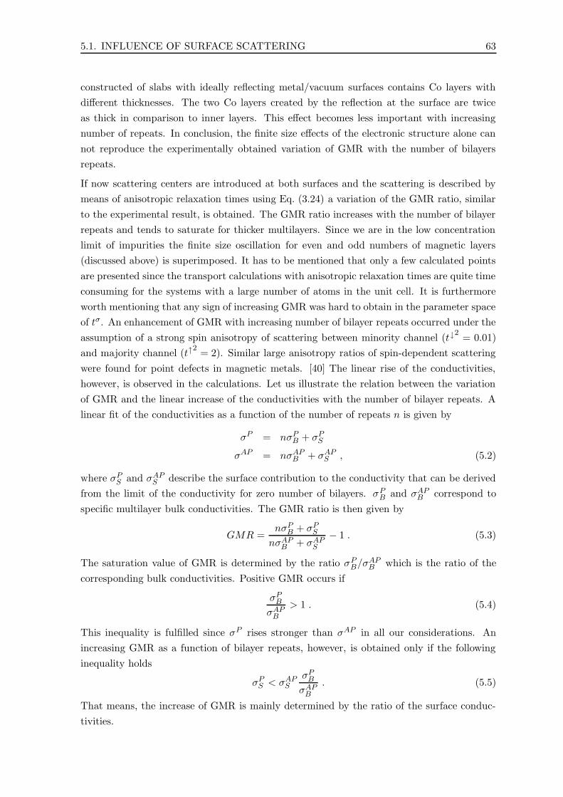
5.1. INFLUENCE OF SURFACE SCATTERING 63
constructed of slabs with ideally reflecting metal/vacuum surfaces contains Co layers with
different thicknesses. The two Co layers created by the reflection at the surface are twice
as thick in comparison to inner layers. This effect becomes less important with increasing
number of repeats. In conclusion, the finite size effects of the electronic structure alone can
not reproduce the experimentally obtained variation of GMR with the number of bilayers
repeats.
If now scattering centers are introduced at both surfaces and the scattering is described by
means of anisotropic relaxation times using Eq. (3.24) a variation of the GMR ratio, similar
to the experimental result, is obtained. The GMR ratio increases with the number of bilayer
repeats and tends to saturate for thicker multilayers. Since we are in the low concentration
limit of impurities the finite size oscillation for even and odd numbers of magnetic layers
(discussed above) is superimposed. It has to be mentioned that only a few calculated points
are presented since the transport calculations with anisotropic relaxation times are quite time
consuming for the systems with a large number of atoms in the unit cell. It is furthermore
worth mentioning that any sign of increasing GMR was hard to obtain in the parameter space
of tσ. An enhancement of GMR with increasing number of bilayer repeats occurred under the
assumption of a strong spin anisotropy of scattering between minority channel (t↓2
= 0.01)
and majority channel (t↑2
= 2). Similar large anisotropy ratios of spin-dependent scattering
were found for point defects in magnetic metals. [40] The linear rise of the conductivities,
however, is observed in the calculations. Let us illustrate the relation between the variation
of GMR and the linear increase of the conductivities with the number of bilayer repeats. A
linear fit of the conductivities as a function of the number of repeats n is given by
σP = nσPB + σPS
σAP = nσAPB + σAPS , (5.2)
where σPS and σAPS describe the surface contribution to the conductivity that can be derived
from the limit of the conductivity for zero number of bilayers. σPB and σAPB correspond to
specific multilayer bulk conductivities. The GMR ratio is then given by
GMR =nσPB + σPSnσAPB + σAPS
− 1 . (5.3)
The saturation value of GMR is determined by the ratio σPB/σAPB which is the ratio of the
corresponding bulk conductivities. Positive GMR occurs if
σPBσAPB
> 1 . (5.4)
This inequality is fulfilled since σP rises stronger than σAP in all our considerations. An
increasing GMR as a function of bilayer repeats, however, is obtained only if the following
inequality holds
σPS < σAPSσPBσAPB
. (5.5)
That means, the increase of GMR is mainly determined by the ratio of the surface conduc-
tivities.
64 5. GIANT MAGNETORESISTANCE
Another confirmation that the investigated phenomenon is related to scattering at the surfaces
can be found in the calculations of Blaas et al. [156]. In this work CIP-GMR of a finite
multilayer is deduced from the electronic structure of a multilayer embedded in an otherwise
semi-infinite system. The conductivity, however, is not calculated for the infinite system but
for the truncated subsystem (see Eq.1 in Ref. [156]). The boundary conditions which are
introduced by this procedure can be interpreted in terms of an arbitrary surface scattering.
As a result the authors obtain the correct variation of the GMR with the number of repeats
for a Co/Pt multilayer although they do not include any scattering otherwise.
The dependence of GMR on the number of bilayer repeats is a finite-size effect which is
related to scattering at surfaces or at the outermost interfaces if the multilayer is grown on a
buffer or protected by a nonmetallic cap layer. The theoretical results demonstrate that the
finite-size effects of the electronic structure are not able to explain the experimental results.
Surface scattering, however, breaks the translational symmetry. As a consequence the finite
size of the system shows up in the dependence of the GMR ratio as a function on the number
of bilayer repeats.
5.2 Influence of interface scattering
The real structure of the multilayers grown and investigated in experiment are much more
distorted and disturbed on the atomic scale than can ever be described by an ab initio
electronic structure method. So the theoretical methods have to be improved to describe
the key features of the nanostructures and the resulting physical properties correctly. With
respect to the transport properties of magnetic multilayers the theoretical methods became
much more powerful. As a result, the gap between the idealized structures investigated
by the theoreticians and the real structures revealing the physical effect could be bridged
to some extent. This development is sketched in Fig. 5.6. First ab intio calculations for
ballistic transport in point contacts [38] or diffusive transport using the isotropic relaxation
time approximation [37] assumed ideal samples sketched in Fig. 5.6(a). It was shown by
several authors [36, 38, 120, 37] that GMR in magnetic multilayers is strongly influenced
by the electronic structure of the system as a function of the magnetic configuration, it is
the difference in Fermi velocities of the multilayers for parallel or antiparallel alignment of
magnetic moments in adjacent magnetic layers that establish GMR by themselves. Since
this effect is a result of Bragg reflection in ideal multilayers it might be less important in
dirty samples which still have a remarkable GMR amplitude. Consequently, spin-dependent
scattering [20, 29, 121, 24, 26, 122] is assumed to play a crucial role for GMR. Although this
fact was accepted generally the question was still open if bulk or interface scattering dominates
the effect. For this purpose a simplified model for the scattering potential was introduced
to investigate the position dependence of defects on the GMR effect [94]. Furthermore the
influence of an ordered c(2x2) alloy was investigated [96]. These defect configurations are
sketched in Fig. 5.6(b). In recent experiments it succeeded to vary the defect configuration
in GMR samples in a reproducible and controllable manner. It was done by the insertion
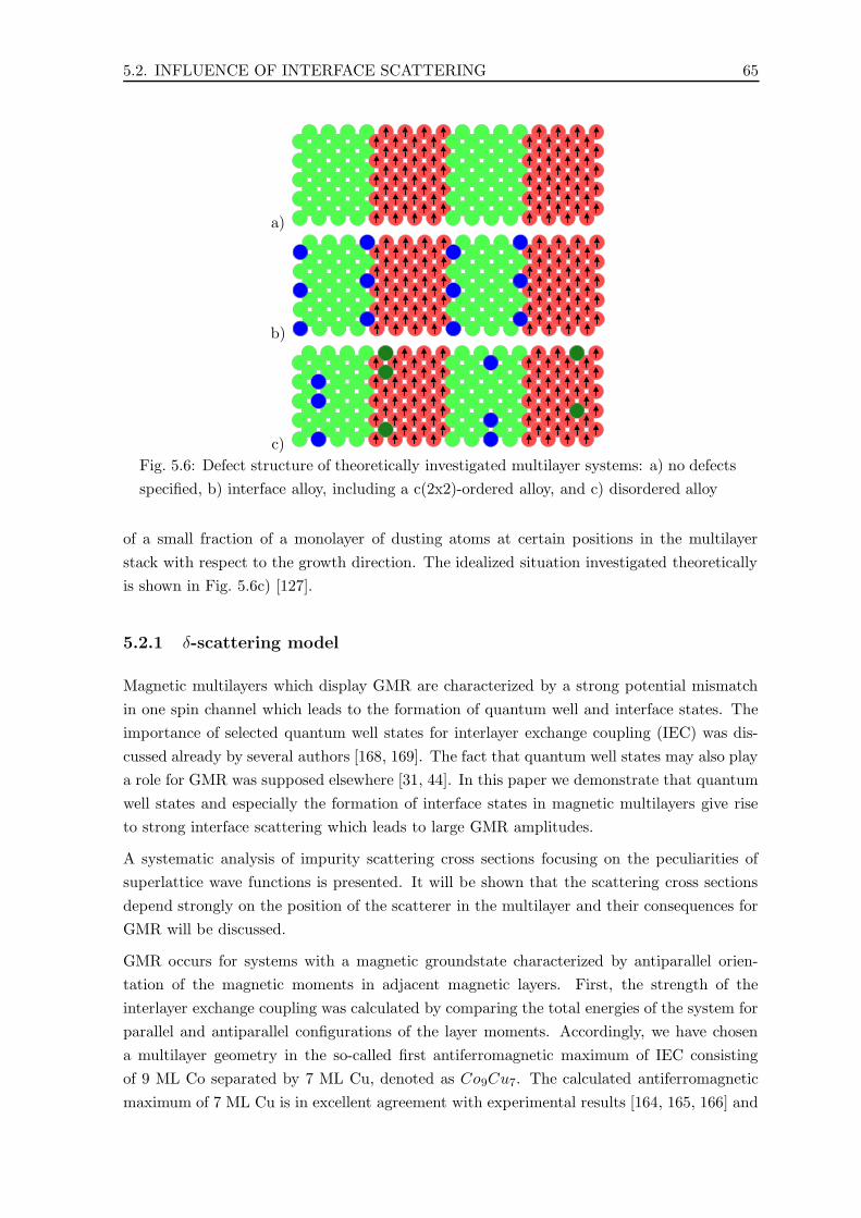
5.2. INFLUENCE OF INTERFACE SCATTERING 65
a)
b)
c)
Fig. 5.6: Defect structure of theoretically investigated multilayer systems: a) no defects
specified, b) interface alloy, including a c(2x2)-ordered alloy, and c) disordered alloy
of a small fraction of a monolayer of dusting atoms at certain positions in the multilayer
stack with respect to the growth direction. The idealized situation investigated theoretically
is shown in Fig. 5.6c) [127].
5.2.1 δ-scattering model
Magnetic multilayers which display GMR are characterized by a strong potential mismatch
in one spin channel which leads to the formation of quantum well and interface states. The
importance of selected quantum well states for interlayer exchange coupling (IEC) was dis-
cussed already by several authors [168, 169]. The fact that quantum well states may also play
a role for GMR was supposed elsewhere [31, 44]. In this paper we demonstrate that quantum
well states and especially the formation of interface states in magnetic multilayers give rise
to strong interface scattering which leads to large GMR amplitudes.
A systematic analysis of impurity scattering cross sections focusing on the peculiarities of
superlattice wave functions is presented. It will be shown that the scattering cross sections
depend strongly on the position of the scatterer in the multilayer and their consequences for
GMR will be discussed.
GMR occurs for systems with a magnetic groundstate characterized by antiparallel orien-
tation of the magnetic moments in adjacent magnetic layers. First, the strength of the
interlayer exchange coupling was calculated by comparing the total energies of the system for
parallel and antiparallel configurations of the layer moments. Accordingly, we have chosen
a multilayer geometry in the so-called first antiferromagnetic maximum of IEC consisting
of 9 ML Co separated by 7 ML Cu, denoted as Co9Cu7. The calculated antiferromagnetic
maximum of 7 ML Cu is in excellent agreement with experimental results [164, 165, 166] and

66 5. GIANT MAGNETORESISTANCE
other calculations [167]. The calculated coupling strength for this system is +1.66mJ/m2.
The structure of the superlattice was assumed to be a fcc lattice with a lattice constant of
6.76 a.u. Lattice distortions and mismatches are neglected. This is justified by structural
investigations where the mismatch between Co and Cu was found to be small and epitaxial
layer-by-layer growth was obtained under certain conditions [170]. An important ingredient
0
1
2
3
0
5
10
15
n(
r,E
F)
[1/R
y]
Co Cu
a)Maj.
Min.
0.0
0.1
0.0
0.2
0.0
0.2
0.0
0.1
|ψk(
r)|2
Co Cu
b)
c)
d)
e)
Fig. 5.7: Co9Cu7 in P configuration: local density of states at EF in [a.u.] (a), prob-
ability amplitude of an extended majority state (b) and of different quantum well and
interface states in minority band (c-e) [94]
to the microscopic understanding of the conductivity is the layerwise decomposed density
of states (LDOS). The LDOS are calculated from the diagonal part of the spin-dependent
one-particle Green function of the multilayer system. They can be resolved by means of the
spectral representation of the Greens function into a superposition of probability amplitudes
of all eigenstates at energy E.
The LDOS at EF of the P configuration is shown in Fig. 5.7(a) and is nearly the same at
all monolayers in the majority channel. The minority electrons are characterized by a very
inhomogeneous profil. The LDOS in the Co layers are much higher than in Cu layers. The
largest values are obtained for the Co layers at the interface. This is a general behaviour
independent on Co or Cu layer thicknesses. This profile can easily be interpreted by means
of probability amplitudes of the eigenstates. Due to a smooth potential profile most of the
eigenstates in the majority bands are extended with a continuous probability amplitude for
all layers [Fig. 5.7(b)]. In contrast, the minority electrons move in a multi-well potential with

5.2. INFLUENCE OF INTERFACE SCATTERING 67
a periodicity perpendicular to the layers (z-direction). For this reason quantum well states
appear which are well localized in z-direction but extended in plane. Besides quantum well
states with a localization in the center of the Co and Cu layers [Fig. 5.7(c),(d)] pronounced
interface states in the Co layer are formed as shown in Fig. 5.7e). The interface state can be
understood in terms of resonant scattering and compares to the virtual bound state of a Co
impurity in a Cu matrix [171].
In the AP configuration both spin channels are dominated by quantum well states. On aver-
age, these Bloch states are less extended than states in the majority band and less localized
than in the minority band. The localization of the eigenstates determine the propagation of
the electrons which has a direct influence on the transport properties.
Since the relaxation time in Eq. (3.24) is proportional to the spin-dependent LDOS at the
impurity site a strong position dependence of the conductivities is expected. Because of
the large enhancement of LDOS at the Co interface layer impurities in these positions will
be the most effective scatterers in comparison to all other positions. Furthermore, from
the knowledge of spectral weights and probability amplitudes, it can be concluded that Co
quantum well states are strongly scattered by defects at the interface position. The results
for GMR as a function of the impurity position in the supercell are shown in Fig. 5.8. The
0.0
0.5
1.0
1.5
2.0
2.5
3.0
Defect PositionCo Cu
GMR
Fig. 5.8: GMR of Co9Cu7: open symbols CIP-GMR, closed symbols for CPP-GMR,
tσ = 0 dashed and full line, β = 0.25 squares, β = 1.0 triangles, β = 4.0 circles. [94]
case of vanishing tσ describes the scattering at homogeneous distributed defects causing an
averaged spin-independent relaxation time τ , see Eq. (3.24), which leads to straight lines at
30% for CIP- and 125% for CPP-GMR. The triangles show GMR results for one impurity
with no spin anisotropy [Eq. (3.23)] (β = 1) at the corresponding position in the supercell.
The influence of a scatterer in the non-magnetic Cu layer is comparatively smaller for both
current directions. This is caused by the small LDOS in these layers for both magnetic
configurations, compare a). On the contrary, the GMR amplitude is strongly influenced by
defects in the ferromagnetic layer, especially at the interfaces. If we assume spin-dependent
scattering with an anisotropy ratio β > 1, that is stronger scattering of minority electrons, this

68 5. GIANT MAGNETORESISTANCE
tendency is enhanced. GMR amplitudes can be enlarged by a factor of 2. For opposite spin
anisotropy β < 1 the spin anisotropy of the local density of states compensates that from the
scattering and GMR is reduced in comparison to spin-independent scattering. From residual
resistivities of dilute alloys [103, 39, 172] it is well known that, depending on the valence
difference between impurity atom and host, opposite spin anisotropies exist. Consequently,
impurities with β > 1 at the Co interface position should cause large GMR amplitudes. In
particular, Cu impurities in bulk Co have an anisotropy of β = 1.85 [127].
Using wave functions of a periodic multilayer, it could be shown that quantum well and
interface states give large contributions mainly to CIP conductivity whereas CPP conductivity
is caused by extended states. Due to quantum well and interfaces states the GMR amplitude
depends strongly on the position of scatterers and favors interface scattering in agreement
with experiment [173]. The calculations suggest that smooth interfaces with impurities in
the Co layer and with large β values leads to high GMR amplitudes in Co/Cu multilayers.
5.2.2 c(2x2)-ordered interface alloy
The following investigations are focused on the magnetotransport properties of ordered inter-
face alloys in a Co/Cu(001) multilayer system. In the context of magnetoelectronics appli-
cations structural properties of the interfaces in nanostructured devices have attracted huge
attention. Especially, the properties of the ferromagnet/nonmagnet (FM/NM) interface are
expected to be crucial for new phenomena like the oscillatory interlayer exchange coupling
and GMR that occur in magnetic layered systems. Several experiments have shown that
even in the best homoepitaxially grown samples interdiffusion at the interfaces exists. The
formation of, even partially ordered surface alloys on a Cu(001) substrate was reported for,
e.g. Mn [174], Fe [175, 176] and Co [177]. Experiments on Co/Cu spin valve systems have
shown the high sensitivity of the magnetotransport on the interface properties by introduc-
ing 3d scattering centers at various positions in the Co and Cu layer [161]. The Co/Cu(001)
system is a model system for magnetism in systems with reduced dimension [178]. The lat-
tice mismatch is rather small (about 2%) and the materials are completely immiscible in
the bulk phase [179]. The systems were modeled as superlattices with a complex unit cell
periodically repeated in 3 dimensions and the electronic structure of the considered systems
was calculated self-consistently. That means, we consider infinite multilayer structures and
exclude the influence of surfaces. The Co layer thickness was fixed to 9 ML, ≈ 16A following
the experimentally investigated systems. We neglect all lattice relaxations at the interfaces.
All atomic positions are fixed to an ideal fcc lattice with a lattice constant of 6.76 a.u.. The
chosen lattice constant lies between the bulk lattice constant of magnetic fcc Co (6.7 a.u.)
and fcc Cu (6.83 a.u.). To simulate the c(2x2) ordered interface alloy we increase the cross
section of the supercell by a factor of 2. Every atomic layer is represented by 2 atoms in the
unit cell. In the Co interface layers one of the Co atoms is replaced by a 3d element (V, Cr,
Mn, Fe, Co, Ni, and Cu, respectively).
It was shown by several authors [6, 94, 180, 181, 182] that the structural properties of the

5.2. INFLUENCE OF INTERFACE SCATTERING 69
interfaces play an important role for the interlayer exchange coupling and GMR. The interface
structure depends strongly on growth conditions during the preparation process. Besides
mesoscopic roughness and interdiffusion the formation of an ordered interface alloy may
occur.
First of all we will discuss the stability of the interface alloys in a Co/Cu multilayer. For this
purpose we compare the total energy of three different interface configurations: 0) the ideal
atomically flat interface with c(1x1) symmetry, 1) one intermixed interface layer with the same
number of Co and Cu atoms equally distributed with c(2x2) symmetry, and 2) two intermixed
interface layers with c(2x2) symmetry. The considered superlattice of type 0 consist of 9 ML
Co and 7 ML Cu. For type 1 and 2 the number of Co layers is reduced by the intermixed
layers to keep the Cu thickness constant. All energies are normalized to an interface area
of the c(1x1) structure. We obtain the following formation energies: 190 meV for the ideal
interfaces, 240 meV for one intermixed atomic layer and 410 meV for two intermixed interface
layers. The energetical most favorable configuration is the ideal Co/Cu interface. This result
is in line with the immiscibility of the materials at low temperatures. The energy difference
of 50 meV between the ideal and the one intermixed layer configuration is of the order of the
total energy difference resolution of our method. Kinetic reasons during the growth process
can however stabilize the configuration with one intermixed layer. These results indicate that
the c(2x2) structures can really occur at interfaces in Co/Cu multilayers. The existence of
c(2x2) structures at surfaces of Co on Cu(001) was already shown experimentally [177].
In the following the magnetic behavior of the c(2x2) interface alloys will be discussed. We
denote the alloy constituents by impurities in the sense of a periodic impurity arrangement
in the interface atomic layer. The local density of states is comparable to that obtained for
3d impurities in bulk Co [183]. For V, Cr and Mn we obtain a sharp virtual bound state
above the Fermi level. The magnetic moments of the impurities are shown in Fig. 5.9. For
V Cr Mn Fe Co Ni Cu−3−2−1
012
µ
Fig. 5.9: Magnetic moments of the 3d constituents of an ordered c(2x2) interface alloy
Co(3d) at the Co/Cu(001) interface
the early 3d impurities V, Cr, and Mn our calculation yields the antiferromagnetic alignment
of the impurity moment relative to the Co moment as ground state. For the second half of
the 3d series Fe, Ni and Cu the ferromagnetic state is energetically preferred. The size of the
local moment nearly follows Hund’s rule with a maximum at half d-band filling.
For the calculation of transport properties we use Mott’s two-current model [118] neglecting

70 5. GIANT MAGNETORESISTANCE
spin flip scattering. For the considered systems assuming only non-Kondo-impurities this
assumption should be reasonable. The linearized Boltzmann equation in relaxation time ap-
proximation was solved and the spin dependent conductivity σσ is obtained from a Fermi
surface integral weighted with an isotropic relaxation time neglecting the anisotropy of the
scattering operator. Assuming the same spin independent relaxation times τ for both mag-
netic configurations of the Co moments (P,AP) this quantity does not enter the expression for
the GMR ratio. In Fig. 5.10 (upper panels) the spin resolved conductivity contributions for
V CrMnFe Co Ni Cu0.0
0.2
0.4
0.6GMR
0.0
1.0
2.0 σP
σAP
0.0
1.0
σmaj
σmin
V CrMnFe Co Ni Cu0.0
0.5
1.0
1.5
2.00.0
1.0
2.0
0.0
1.0
CIP CPP
Fig. 5.10: Spin resolved conductivities for the P configuration (top panels), conductivi-
ties for P and AP configuration (central panels) and GMR ratio (lower panels) for CIP
and CPP transport in dependence on interface alloy constituent
the P configuration are shown in dependence on the interface alloy constituent. The conduc-
tivities are calculated for current in-plane (CIP) and perpendicular-to-plane (CPP) geometry.
For defects with a moment parallel to the Co magnetization a large spin anisotropy occurs.
The conductivity is dominated by the fast majority channel, especially pronounced in the
CPP geometry. The occurrence of one dominating spin channel in the P configuration is
essential to establish a large GMR ratio. In Co/Cu systems the majority potential for both
materials is nearly equal whereas the minority potential has strong quantum well modula-
tions. For the AP configuration the effective potential for both spin channels is a mixing
of majority and minority potentials and causes averaged conductivities. The same effect is
produced by defects with an antiparallel moment relative to the Co moment causing a strong
perturbation of the majority potential even in the P configuration.

5.3. POSITION AND MATERIAL DEPENDENCE 71
In Fig. 5.10 (central panel) the total conductivities for the P and AP configuration are com-
pared. The relative difference determines the GMR ratio. We obtain a CIP-GMR ratio of
31% for the system with ideal interfaces. For the alloys of Fe, Ni, and Cu with a moment
parallel to the Co moment the value is increased by nearly a factor of 2. In the contrary, for
systems with alloys of V, Cr, and Mn with antiparallel moment the CIP-GMR ratio is reduced
systematically. As a result, we can conclude the following empirical rule for the influence of
interface alloys on CIP transport. Magnetically ordered structures with moments parallel to
the ferromagnetic layers increase the GMR ratio whereas alloy constituents with antiparallel
moments decrease the ratio.
In CPP geometry the GMR ratio changes by about 60% for alloys with parallel moments. In
the case of antiparallel moment of the alloy constituent the spin asymmetry of the conductiv-
ity in the P configuration changes the sign and the conductivity is dominated by the minority
channel. Additionally, the conductivity for AP configuration decreases rapidly for the earlier
3d elements and causes a strong enhancement of GMR for V and Cr interface alloys.
In summary, the GMR ratio is mainly determined by the difference of the coherent potential
surface of the layered structure for P and AP configuration. As a consequence a fast and slow
channel are obtained in P configuration expressed by the spin asymmetry of the conductivity.
Since the potentials are mixed in the AP configuration the fast channel is closed. This causes
the resistivity drop and is the origin of GMR. The GMR ratio decreases rapidly with the
vanishing spin asymmetry of the conductivity in P configuration due to alloy formation.
Magnetically ordered structures with moments antiparallel to the ferromagnetic layers (V,
Cr, and Mn, respectively) reduce the spin asymmetry and the GMR ratio. In contrary, alloy
constituents with moments parallel to the Co moments increase the spin asymmetry of the
conductivity in P configuration and accordingly increase the GMR ratio.
5.3 Position and material dependence
Several authors have shown [184, 185] that GMR in magnetic multilayers is strongly influ-
enced by changes in the electronic structure, especially the Fermi velocities, of the system in
dependence on the relative magnetization alignment in adjacent layers. In realistic samples,
however, spin-dependent scattering is considered to cause GMR. The effort to tailor GMR
systems with high rates was accompanied by a variety of experiments [173, 161] and calcu-
lations [122, 94, 46] which investigated the influence of dusting and doping by impurities.
Agreement was reached concerning the dominant role of interface scattering [173]. The re-
sults of Marrows et al. [161], however, demonstrated the strong dependence of GMR on
the position of the impurities with respect to the interfaces and on the valence difference
between impurity and host. The aim of these calculations was to determine scattering cross
sections and resulting GMR ratios from ab initio. They are focused on the dependence on
defect material and position for one of the standard systems of magnetoelectronics Co/Cu.
[127]

72 5. GIANT MAGNETORESISTANCE
We have chosen a multilayer geometry in the so-called first antiferromagnetic maximum of
interlayer exchange coupling consisting of 9 monolayers (ML) Co separated by 7 ML Cu,
denoted as Co9Cu7. The structure of the superlattice was assumed to be an fcc lattice with
a lattice constant of 6.76 a.u. grown in (001) direction. Each atomic plane is represented by
one atom in the prolonged unit cell with 32 atoms.
The impurity potential at a defined position in the superlattice is calculated self-consistently.
Charge relaxations up to the second atomic shell around the impurity atom are considered.
The Greens function of the multilayer with impurity is calculated by solving the Dyson
equation.
Based on this information the microscopic spin-conserving transition probability P σkk′ for
elastic scattering, that is on-shell-scattering of a superlattice Bloch wave k at an impurity
atom into a perturbed state k′ is calculated by Fermi’s Golden rule in Eq. (3.13). Spin-orbit
coupling and the resulting spin-flip processes are neglected by the non-relativistic scheme.
Summation over all final states leads to the spin and state dependent relaxation time τ σk (µ) =[∑k′ P
σkk′(µ)
]−1, which depends on the site index µ of the impurity position in the multilayer.
The k and spin-dependence of the scattering rates is treated fully quantum-mechanically
without adjustable parameter. Up to this point we consider a dilute alloy of impurity atoms
all of them occupying a chosen site µ in the unit cell. That is, the alloying is restricted to
certain atomic planes in the multilayer. These planes correspond to the impurity δ-layers
experimentally investigated by Marrows and Hickey [161].
The conductivity is calculated by solving the quasi-classical Boltzmann equation (3.10) which
depends now on the position µ and the species of the considered defect. Thus, the vector
mean free paths are obtained by
Λkσ(µ) = τσk (µ)
[vσk +
∑
kk′P σkk′(µ)Λk′
σ(µ)
]. (5.6)
This includes besides to the anisotropic relaxation times as the second term on the r.h.s
the computational demanding scattering-in term (vertex corrections) which describes the
anisotropy of the scattering as discussed in section 3.3 and completes the description of im-
purity scattering [186, 40]. A detailed analysis of the asymmetry of the scattering probabilities
as introduced in Eq. (3.32) is in progress. The band structure is included via Fermi velocities
vσk and the k′ summation over all states on the anisotropic Fermi surface. The impurity
scattering enters via the relaxation times τ σk (µ) and the microscopic transition probabilities
P σkk′(µ). To our knowledge, this was the first semi-classical calculation of GMR beyond the
mostly applied relaxation time approximation [20, 24, 37, 44, 94, 46] , which neglects the
scattering-in term. Zhang and Butler proposed a simplified method to include the vertex
corrections by renormalization of the electron life times using an adjustable parameter [117].
Based on the solution of Equation (5.6) the spin-dependent conductivity tensor σσ(µ) is
given by a Fermi surface integral following Eq. (3.39) and depends on the defect position and
species. With Mott’s two current model [118] the total conductivity σ(µ) = σ↑(µ) + σ↓(µ) is
obtained by spin summation.

5.3. POSITION AND MATERIAL DEPENDENCE 73
We consider the Co/Cu multilayer described above and investigate the scattering properties of
Cu impurities in the Co layers and Co impurities in the Cu layer. The eigenstates show strong
quantum confinement due to the superlattice potential. That is, the probability amplitude
is modulated by the layered structure and can even tend to zero at particular sites of the
supercell [44, 94]. As a consequence all Bloch states with a nearly zero probability amplitude
at the impurity site undergo a weak scattering and cause extremely large relaxation times.
The anisotropy of the scattering can be characterized much more descriptive by the spin and
state dependent relaxation times, rather than by the resulting vectors of mean free paths
including the vertex correction effects. The state dependent relaxation times are distributed
over several orders of magnitude, especially for defects inside the metallic layers as shown in
Fig. 5.11 by the probability n[norm.] to find a state with a given logarithm of the relaxation
time. This is a new effect that was never obtained in bulk systems and is related to the
modulation of the Bloch states due to the layered structure [94]. The analysis of the transport
100 101 102 103 104105 106 107
0.0
0.2
0.4
0.6
0.8
1.0
n [no
rm.]
τ [fs at%]100 101 102 103 104
105 106 1070.0
0.2
0.4
0.6
0.8
1.0
n [no
rm.]
τ [fs at%]
"!$#%&
100 101 102 103 104105 106 107
0.0
0.2
0.4
0.6
0.8
1.0
n [no
rm.]
τ [fs at%]100 101 102 103 104
105 106 1070.0
0.2
0.4
0.6
0.8
1.0
n [no
rm.]
τ [fs at%]
' )(*+,.-/(
100 101 102 103 104105 106 107
0.0
0.2
0.4
0.6
0.8
1.0
n [no
rm.]
τ [fs at%]100 101 102 103 104
105 106 1070.0
0.2
0.4
0.6
0.8
1.0
n [no
rm.]
τ [fs at%]
"-/(01(0
Fig. 5.11: Distribution of relaxation times for both spin directions caused by Cu impu-
rities in Co bulk and at the Co interface and center sites of a Co9/Cu7(001) multilayer
in parallel magnetic configuration, the vertical lines mark the averaged relaxation by
Eq. (3.12)
coefficients is focused on the current-in-plane (CIP) geometry. The total CIP-conductivities
caused by Co impurities at different positions in the Cu layer and Co defects in the Cu
layer are shown in Fig. 5.12(a) for both configurations of the Co magnetization (P, AP). The
conductivity differs by orders of magnitude as a function of impurity position (keep in mind
the logarithmic scale). The largest values occur for impurity positions where the quantum
confinement produces many Bloch states with low probability amplitude. These states with
large relaxation times, although not numerous, are highly conducting and nearly provoke
a short circuit. This effect is mainly obtained for impurities in the center of the layers.
This behavior is caused by the corresponding velocity components of Bloch states in current
direction, that is, all confined states like quantum well and interface states have mainly a
group velocity in direction of the planes and contribute mostly to the CIP conductivity [94].

74 5. GIANT MAGNETORESISTANCE
110
1001000 a)
Co layerCu layer
σ || [at%
/µΩ
cm]
P
AP
0,25
1
4
b)
σ || [at%
/µΩ
cm]
P
AP
Fig. 5.12: Conductivity of Co9Cu7 for P and AP alignment in dependence on the
position of Co impurities in Cu layer (left) and Cu impurities in Co layer (right), a)
Assuming scattering at the inserted δ-layer only, b) Assuming δ-layer scattering (50%)
and interface scattering (50%)
This peculiar behavior of conductivity is in agreement with the results of Blaas et al. [46]
who found higher resistivities with interdiffusion restricted to the interface layers than for
alloying with Cu atoms in the Co layers.
For comparison with experiments we have to mention that the large absolute values would
hardly be obtained experimentally since they correspond to idealized samples with perfect
flat interfaces and defects at well defined positions in the superlattice. As soon as we con-
sider an overall distribution of defects in the multilayer the highly conducting channels are
suppressed. This phenomenon of highly conducting electron channels confined to one layer
of a multilayer structure is called electron wave guide or channeling effect [44, 130] and was
also experimentally verified [187].
Structural investigations of Co/Cu multilayers on an atomic scale [188, 189] gave evidence that
most of the structural imperfections appear next to the interfaces. To investigate the influence
of more than one type of scattering center in one sample a simplified defect distribution was
assumed. To describe the existence of an overall distribution of non-interacting impurities in
the multilayer, layer-dependent relaxation times τ σk (µ) are superimposed
1
τσk=∑
µ
x(µ)
τσk (µ), (5.7)
including weighting factors x(µ) that account for the relative concentration of defects at the
corresponding positions µ in the unit cell. The conductivity is then calculated in relaxation
time approximation Λσk = τσk vσk . In addition to the specific δ-layer, Co defects in the Cu
interface atomic layer and Cu defects in the Co interface atomic layer are considered to
simulate an intermixed region at the interface. For the concentration weights x(µ) entering
equation (5.7) we choose 25% for defects in each interface layer and 50% for defects in the
δ-layer and the resulting conductivities are shown in Fig. 5.12(b). The GMR ratios derived
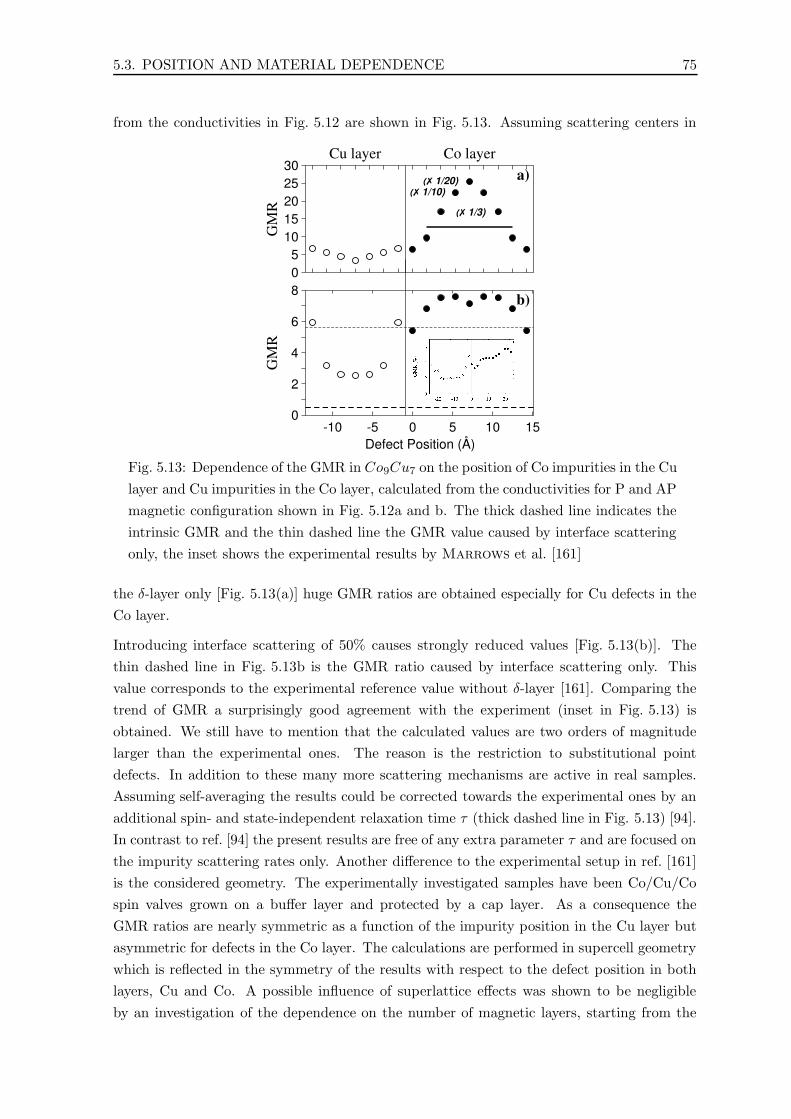
5.3. POSITION AND MATERIAL DEPENDENCE 75
from the conductivities in Fig. 5.12 are shown in Fig. 5.13. Assuming scattering centers in
05
1015202530
Co layerCu layer
(7 1/3)
(7 1/10)(7 1/20)
0 5 10 15-5-10Defect Position (Å)
0
2
4
6
8G
MR
GM
R
a)
b)
effect is larger for Ni—almost 50% higher. One possibleinterpretation is that the d-layer forms a second highly effec-tive spin-filter just behind the first filter of the Co/Cu inter-face. Although no value is reported in Ref. 13 for Ni, thevalue of aFe512 given for Fe in Co leads one to supposethat the value of aNi must also be @1, and likely to be evenhigher still than the value for Fe.
The effects of Cu impurities are also of particular interest.When close to the interface there is little effect, or a smallsuppression, due presumably to the artificial creation of amore interdiffused, alloyed interfacial layer. However, oncethe Cu is deep inside the layer we see an enhanced GMR,somewhat unexpected in the light of the fact that these arenonmagnetic impurities. An obvious comparison here is withthe large bulk spin anisotropy in the resistivity of Ni layersdoped with Cu observed by Vouille et al.19
Within the group of noble metals, the GMR is lower forAg impurities than for Cu, and lower still for Au. The be-havior is consistent with greater spin-orbit scattering—theheavier elements flip spins more readily, mixing the spincurrent channels. A comparison with, for example, Pd and Ptis consistent; the GMR recovers more rapidly as Pd is movedaway from the Co/Cu interface. Both these elements, withstrong Stoner susceptibility enhancements in the bulk, arereadily polarized by the Co matrix, leading to little loss inGMR.
On the other hand the graphs for Cr, Mo, Ru, Ta, and Wall show that the insertion of the d-layer at the interfacealmost totally suppresses the GMR. As the impurity ismoved back into the Co the GMR rises in a roughly linearfashion. For Ru and Ta the GMR appears to plateau whenthe dopant is ;10 and 20 Å from the interface, respectively.This is exactly the behavior expected given the importanceattached to interfacial scattering, but the length scale isgreater than that of only ;2.5 Å previously reported whenCo d-layers were inserted into NiFe,22 suggesting that thelengthscales involved in discussions of interfacial or bulkscattering must be highly material system dependent. For allof these materials but Ta, the reported a value is ,1. Thevalue of aTa51.23 appears to be an overestimate.
The data for Mn, V, and Nb also look similar. Theseelements have a values reported .1, and we see that thedependence on the position of the dopant layer is quite weak.The GMR is suppressed wherever the d-layer is placed.There is little or no suppression of the GMR when the ele-ments Ti or Zr, both with a.1, are introduced into the in-terfacial region of the Co layer. The effects of Hf are anoma-lous in this regard, possibly either aHf52.5 is anoverestimate, or the high nuclear charge of Hf leads to alarge spin-orbit scattering term. This is to be compared withthe results found for Ta.
It is also of interest to pose the question regarding theeffects of impurities in the Cu spacer layer. The reader’sattention is drawn to Fig. 2, where the GMR of the spinvalves with Co~Cu! impurities in the Cu~Co! layer~s! is pre-sented. The data for the Cu impurities ~solid symbols! istaken from Fig. 1. As we have seen, the GMR rises as the Cumoves back into the Co after a small suppression close to theinterface. On the other hand, Co impurities in the Cu spacer
strongly reduce the GMR with only a weak position depen-dence unless they are close to the interface. We should ex-pect that Co atoms or clusters isolated in the Cu should be-have ~super!paramagnetically, leading to spin-independentscattering when averaging over time or position in the film,as in practical measurements. The decay length of ;10 Å istherefore a direct measure of the range of significant ex-change interactions for the Co impurities in Cu. Further ex-periments with other impurities in the spacer layer are allconsistent with the same general picture: a position indepen-dent suppression of the GMR due to a shortening of themean-free path in the crucial spacer layer, unless the impu-rity is within two or three atomic sites of the interfacial re-gion, where the impurity can begin to affect nature of theinterfacial scattering.
We find that the experimental results are at odds with thepublished theoretical predictions of Zahn et al.20 in the fol-lowing important ways: impurities with a,1 suppress theGMR, usually to a great extent when at the interface, andstill have a considerable effect when several lattice constantsaway from the interface; impurities with a.1 sometimes doprovide an enhancement of the GMR, but it is only to befound when they are a few Å behind the Co/Cu interface;and impurities in the spacer layer have a dramatic effect bylowering the GMR. There are two omissions in the theory ofZahn et al., which may lead to inaccurate predictions: a lackof interband transitions, found to have an important effect onconductivity calculations when realistic levels of disorder areincluded;9 and vertex corrections are required for an accuratedescription of impurity scattering.28
The results of more sophisticated calculations by Binderet al.,29 are qualitatively much more in accord with the ob-servations that we report here. Self-consistently calculatedimpurity potentials were used, as well as a more correct de-scription of the microscopic transport processes includingstate-dependent relaxation times and proper account taken ofthe scattering-in term. In particular, the predictions of thechange in GMR when moving the d-layers of specific mate-rials from the interface in to the bulk of the Co show remark-able similarities with the observations and the sign of thischange exhibits strong correlations with the sign of the ex-change interaction calculated between the local moment ofthe impurity ion and the Co matrix.
FIG. 2. Dependence of the GMR on the position of Co impuri-ties in Cu ~open symbols! or Cu impurities in Co ~solid symbols!.x50 corresponds to the position of the Cu/Co interface.
RAPID COMMUNICATIONS
IMPURITY SCATTERING FROM d-LAYERS IN GIANT . . . PHYSICAL REVIEW B 63 220405~R!
220405-3
Fig. 5.13: Dependence of the GMR in Co9Cu7 on the position of Co impurities in the Cu
layer and Cu impurities in the Co layer, calculated from the conductivities for P and AP
magnetic configuration shown in Fig. 5.12a and b. The thick dashed line indicates the
intrinsic GMR and the thin dashed line the GMR value caused by interface scattering
only, the inset shows the experimental results by Marrows et al. [161]
the δ-layer only [Fig. 5.13(a)] huge GMR ratios are obtained especially for Cu defects in the
Co layer.
Introducing interface scattering of 50% causes strongly reduced values [Fig. 5.13(b)]. The
thin dashed line in Fig. 5.13b is the GMR ratio caused by interface scattering only. This
value corresponds to the experimental reference value without δ-layer [161]. Comparing the
trend of GMR a surprisingly good agreement with the experiment (inset in Fig. 5.13) is
obtained. We still have to mention that the calculated values are two orders of magnitude
larger than the experimental ones. The reason is the restriction to substitutional point
defects. In addition to these many more scattering mechanisms are active in real samples.
Assuming self-averaging the results could be corrected towards the experimental ones by an
additional spin- and state-independent relaxation time τ (thick dashed line in Fig. 5.13) [94].
In contrast to ref. [94] the present results are free of any extra parameter τ and are focused on
the impurity scattering rates only. Another difference to the experimental setup in ref. [161]
is the considered geometry. The experimentally investigated samples have been Co/Cu/Co
spin valves grown on a buffer layer and protected by a cap layer. As a consequence the
GMR ratios are nearly symmetric as a function of the impurity position in the Cu layer but
asymmetric for defects in the Co layer. The calculations are performed in supercell geometry
which is reflected in the symmetry of the results with respect to the defect position in both
layers, Cu and Co. A possible influence of superlattice effects was shown to be negligible
by an investigation of the dependence on the number of magnetic layers, starting from the

76 5. GIANT MAGNETORESISTANCE
trilayer system [95].
2354
0
2
4
6
0 5 10 15 20 25x (A)
GM
R (%
)
Cr α = 0.3
0
2
4
6
0 5 10 15 20 25x (Å)
GM
R (%
)
Mn α = 0.8
0
2
4
6
0 5 10 15 20 25x (Å)
GM
R (%
)
Fe α = 12
0
2
4
6
0 5 10 15 20 25x (Å)
GM
R (%
)
Ni
0
2
4
6
0 5 10 15 20 25x (Å)
GM
R (%
)
Cu
0
2
4
6
0 5 10 15 20 25x (Å)
GM
R (%
)
Zr α = 3.3
0
2
4
6
0 5 10 15 20 25x (Å)
GM
R (%
)
Nb α = 1
0
2
4
6
0 5 10 15 20 25x (Å)
GM
R (%
)
Mo α = 0.7
0
2
4
6
0 5 10 15 20 25x (Å)
GM
R (%
)
Ru α = 0.22
0
2
4
6
0 5 10 15 20 25x (Å)
GM
R (%
)
Pd
0
2
4
6
0 5 10 15 20 25x (Å)
GM
R (%
)
Ag
0
2
4
6
0 5 10 15 20 25x (Å)
GM
R (%
)
Ta α = 1.23
0
2
4
6
0 5 10 15 20 25x (Å)
GM
R (%
)
Pt
0
2
4
6
0 5 10 15 20 25x (Å)
GM
R (%
)
Au
0
2
4
6
0 5 10 15 20 25x (Å)
GM
R (%
)
Co
0
2
4
6
0 5 10 15 20 25x (Å)
GM
R (%
)
V α=1
0
2
4
6
0 5 10 15 20 25
Ir α = 0.33Os α = 0.29Re α = 0.3
Rh α = 1Tc
x (Å)
GM
R (%
)Ti α = 1.4
0
2
4
6
0 5 10 15 20 25x (Å)
GM
R (%
)
W α = 0.4
0
2
4
6
0 5 10 15 20 25x (Å)
GM
R (%
)
Hf α = 2.5
0
2
4
6
0 5 10 15 20 25x(Å)
GM
R(%
)
Al
0
2
4
6
0 5 10 15 20 25x(Å)
GM
R(%
)
Nd
0
2
4
6
0 5 10 15 20 25x(Å)
GM
R(%
)
Gd
0
2
4
6
0 5 10 15 20 25x(Å)
GM
R(%
)
Dy
0 5 10 15x(Å)
0
2
4
6
8
10
GM
R
Ti (α=0.4)
0 5 10 15x(Å)
0
2
4
6
8
10V (α=0.1)
0 5 10 15x(Å)
0
2
4
6
8
10Cr (α=0.04)
0 5 10 15x(Å)
0
2
4
6
8
10Mn (α=1.3)
0 5 10 15x(Å)
0
2
4
6
8
10Fe (α=45)
0 5 10 15x(Å)
0
2
4
6
8
10Co
0 5 10 15x(Å)
0
2
4
6
8
10Ni (α=568)
0 5 10 15x(Å)
0
2
4
6
8
10Cu (α=26)
276840
2
4
6
0 5 10 15 20 25x(A)
GM
R(%
)
Crα=0.3
0
2
4
6
0 5 10 15 20 25x(Å)
GM
R(%
)
Mnα=0.8
0
2
4
6
0 5 10 15 20 25x(Å)
GM
R(%
)
Feα=12
0
2
4
6
0 5 10 15 20 25x(Å)
GM
R(%
)
Ni
0
2
4
6
0 5 10 15 20 25x(Å)
GM
R(%
)
Cu
0
2
4
6
0 5 10 15 20 25x(Å)
GM
R(%
)
Zrα=3.3
0
2
4
6
0 5 10 15 20 25x(Å)
GM
R(%
)
Nbα=1
0
2
4
6
0 5 10 15 20 25x(Å)
GM
R(%
)
Moα=0.7
0
2
4
6
0 5 10 15 20 25x(Å)
GM
R(%
)
Ruα=0.22
0
2
4
6
0 5 10 15 20 25x(Å)
GM
R(%
)
Pd
0
2
4
6
0 5 10 15 20 25x(Å)
GM
R(%
)
Ag
0
2
4
6
0 5 10 15 20 25x(Å)
GM
R(%
)
Taα=1.23
0
2
4
6
0 5 10 15 20 25x(Å)
GM
R(%
)
Pt
0
2
4
6
0 5 10 15 20 25x(Å)
GM
R(%
)
Au
0
2
4
6
0 5 10 15 20 25x(Å)
GM
R(%
)
Co
0
2
4
6
0 5 10 15 20 25x(Å)
GM
R(%
)
Vα=1
0
2
4
6
0 5 10 15 20 25
Irα=0.33Osα=0.29Reα=0.3
Rhα=1Tc
x(Å)
GM
R(%
)
Tiα=1.4
0
2
4
6
0 5 10 15 20 25x(Å)
GM
R(%
)
Wα=0.4
0
2
4
6
0 5 10 15 20 25x(Å)
GM
R(%
)
Hfα=2.5
0
2
4
6
0 5 10 15 20 25x(Å)
GM
R(%
)
Al
0
2
4
6
0 5 10 15 20 25x(Å)
GM
R(%
)
Nd
0
2
4
6
0 5 10 15 20 25x(Å)
GM
R(%
)
Gd
0
2
4
6
0 5 10 15 20 25x(Å)
GM
R(%
)
Dy
0 5 10 15x(Å)
0
2
4
6
8
10
GM
R
Zr (α=0.4)
0 5 10 15x(Å)
0
2
4
6
8
10Nb (α=0.2)
0 5 10 15x(Å)
0
2
4
6
8
10Mo (α=0.1)
0 5 10 15x(Å)
0
2
4
6
8
10Tc (α=0.02)
0 5 10 15x(Å)
0
2
4
6
8
10Ru (α=0.02)
0 5 10 15x(Å)
0
2
4
6
8
10Rh (α=0.2)
0 5 10 15x(Å)
0
2
4
6
8
10Pd (α=12)
0 5 10 15x(Å)
0
2
4
6
8
10Ag (α=41)
Fig. 5.14: Dependence of the GMR on the position of 3d (a) and 4d (b) impurities in the
Co layer; upper row: experimental results by Marrow and Hickey (Fig. 1 from [161]);
lower row: our calculation. x = 0 corresponds to the position of the Cu/Co interface.
α values are calculated for the corresponding impurities in bulk Co
Figure 5.14 compiles the trend of GMR caused by 3d- [Fig. 5.14(a)] and 4d-transition metal
impurities [Fig. 5.14(b)] as a function of position in the Co layer. Experimental results from
ref. [161] are given in the upper row, and the calculated values are given below. The α values
for the anisotropy of the spin-dependent resistivities (Eq. (3.42)) stem from experiment and
calculations for 3d- and 4d-transition metal impurities in bulk Co, respectively.
The general trend of the absolute values of GMR as a function of impurity is well reproduced if
we concentrate on the comparison of the results between x=0-8A since geometry and total Co
layer thickness differ in experiment and calculation. Impurities with a scattering anisotropy
α > 1 (Fe, Ni, Cu, Pd, Ag) cause larger GMR values, whereas impurities with α < 1 give
rise to lower GMR rates with respect to the Co reference value. Even the opposite influence
of the isovalent elements Fe and Ru is reproduced. Fe impurities with high spin anisotropy
(α = 45) cause a strong GMR effect whereas the non-magnetic Ru impurities cause strong
scattering in both spin channels (α = 0.02) and lead to suppression of GMR.
The dependence of the GMR ratio as a function of impurity position is in most of the cases
very well reflected (consider, e.g., V, Cr, Mn, Cu or Mo, Ru, Pd). A discrepancy between
theory and experiment exists for Ti and Zr. The measurements obtain a decrease of GMR
moving the δ-layer from the interface into the center of the layer. The calculations predict

5.3. POSITION AND MATERIAL DEPENDENCE 77
an increase. The related spin anisotropies are also opposite (αexp > 1 and αtheory < 1).
This discrepancy could arise from the large atomic volume and the related lattice relaxation
around the impurity atom which is not taken into account in the calculation. The same
discussion holds for the noble metal impurities (Ag). The increase of GMR moving the δ-
layer from the interface into the Co layer is very well reflected for Cu impurities. Isovalent but
larger Ag impurities, however, show a much stronger change in the experimental results than
in the calculation. Furthermore, the calculated changes of GMR as a function of impurity
position for Fe and Ni are less pronounced. This is probably related to the neglect of spin-flip
scattering which is going to be important in systems with large spin anisotropy [40] and the
neglect of any other spin-dependent scattering mechanism.
In conclusion, the self-consistent calculation of the scattering properties and the improved
treatment of the Boltzmann transport equation including vertex corrections provide a power-
ful tool for a comprehensive theoretical description and a helpful insight into the microscopic
processes of CIP-GMR. The experimentally found trends concerning the doping with various
materials at different positions in the magnetic multilayer could be reproduced for many dif-
ferent systems which means that spin-dependent impurity scattering is the most important
source of GMR. The theoretical results show furthermore that interface scattering caused
by intermixing plays a crucial role and has to be taken into account in any system under
consideration. Selective doping of the multilayer with impurities in specific positions causes
variations of GMR which could be well understood by the modulation of spin-dependent
scattering due to quantum confinement in the layered system and by the spin anisotropy α
of the resistivities. The scale of discrepancies between calculations and experiments has to
be considered as a measure of the importance of additional scattering processes.


Chapter 6
Summary and outlook
A powerful formalism for the calculation of the residual resistivity of metallic nanostructured
materials without adjustable parameters is presented. The electronic structure of the unper-
turbed system is calculated using a screened KKR multiple scattering Greens function formal-
ism in the framework of density functional theory. The linear scaling of the numerical effort
allows for the treatment of systems with realistic dimensions comparable to experimentally
investigated samples. The scattering potential of point defects is calculated self-consistently
by solving a Dyson equation for the Greens function of the perturbed system. Assuming a
low concentration of defects (dilute limit) the scattering probability of the electrons (quasi-
particles) is derived from the scattering matrix of the single defects. This formalism was
expanded and applied to defects in metallic nanostructures for the first time. Using the ab
initio scattering probabilities the residual resistivity and conductivity were calculated using
the quasi-classical Boltzmann equation.
Based on ab-initio calculations of the conductivity of Cu/Co slabs we have shown that the
conductance anomalies during growth can be explained by the changes of the electronic
structure as a function of the film thickness. A pronounced conductivity drop is obtained
when the first Co layer is deposited on top of the Cu, in contrast to the increasing conductance
in the general case. Due to interaction of the Co d-electrons with the Cu s-electrons the
character of the minority Fermi surface is changed from sp to d-like. As a consequence,
the local conductivity contributions of the Cu layers are reduced. Since the total DOS at
the Fermi level is still increasing during film growth the effect is related to reduced Fermi
velocities. This microscopic picture can be generalized to any multilayer consisting of noble
and transition metal layers, e.g. Fe/Ag, Cr/Au, and Permalloy/Cu.
The GMR ratio is mainly determined by the difference of the coherent potential surface
of the layered structure for parallel (P) and antiparallel (AP) magnetic configuration. As
a consequence a fast and slow channel are obtained in P configuration expressed by the
spin asymmetry of the conductivity. Since the potentials are mixed in the AP configuration
the fast channel is closed. This causes the resistivity drop and is the origin of GMR. In
multilayer systems the pronounced difference of the transport in growth direction (CPP) and
perpendicular to this direction (CIP) were investigated.
79

80 6. SUMMARY AND OUTLOOK
We have shown using wave functions of a periodic Co/Cu multilayer that quantum well
states and interface states give large contributions mainly to CIP conductivity whereas CPP
conductivity is caused by extended states. The results assuming a simplified δ-scattering
model demonstrate that, due to quantum well and interface states, the GMR amplitude
depends strongly on the position of the scatterers and favors interface scattering in agreement
with experiment. The calculations suggested that smooth interfaces with impurities in the
Co layer and with large spin anisotropies of the scattering (β > 1) lead to high GMR ratios.
The GMR ratio of Co/Cu multilayers with ordered c(2x2) interface alloys of different materi-
als decreases rapidly with the vanishing spin asymmetry of the conductivity in P configuration
due to alloy formation. Magnetically ordered structures with moments antiparallel to the fer-
romagnetic layers (V, Cr, and Mn, respectively) reduce the spin asymmetry and the GMR
ratio. In contrary, alloy constituents with moments parallel to the Co moments increase the
spin asymmetry of the conductivity in P configuration and accordingly increase the GMR
ratio.
The experimentally found trends concerning the doping of Co/Cu multilayers with various
materials at different positions could be reproduced for many different systems, which means
that spin-dependent impurity scattering is an important source of GMR. The theoretical
results show furthermore that interface scattering caused by intermixing plays a crucial role
and has to be taken into account in any system under consideration. Selective doping of the
multilayer with impurities in specific positions causes variations of GMR which could be well
understood by the modulation of spin-dependent scattering due to quantum confinement in
the layered system and by the spin anisotropy of the scattering. The scale of discrepancies
between calculations and experiments has to be considered as a measure of the importance
of additional scattering processes.
The importance of vertex corrections in the solution of the Boltzmann equation is demon-
strated. They modify the deviation of the distribution functions from equilibrium for quite a
few states. In contrast, it turned out that the influence on the conductivity integral is small
for most systems, due to the contribution of all states near the Fermi level.
In conclusion, the self-consistent calculation of the scattering properties and the improved
treatment of the Boltzmann transport equation including vertex corrections provide a pow-
erful tool for a comprehensive theoretical description and a helpful insight into the microscopic
processes determining the transport properties of magnetic nanostructured materials.
Future projects are devoted to the conductance of ultrathin metallic films, investigating the
influence of defects, adatoms, and small clusters adsorbed on or in the surface. Furthermore
the influence of voids or holes causing a local constriction for the electron transport will be
considered.
The inclusion of spin-orbit-coupling will provide information about the spin scattering. The
spin diffusion length often denoted as the decisive length to obtain a conductance response
from magnetic rearrangements in magnetic multilayers will be accessible.

Appendix A
Formal solution of Boltzmann
equation
To solve the Boltzmann equation in the form of Eq. (3.8) or Eq. (3.10) different numerical
schemes were developed. In the following the exact solution in k-space, the degenerate kernel
solution, the variational solution, and the Ziman solution will be sketched. Their numerical
effort concerning the computational power and/or the neccessary memory space is much
larger than for the iterative scheme, which was used throughout this work and was discussed
in paragraph 3.1.1. The required memory space in this case is determined by the considered
cluster size of the defects. The deviation of the solution from the exact one can be controled
by an accuracy parameter. By the exact solution in k-space and the degenerate kernel solution
the exact solution of Eq. (3.8) is obtained, but the highest numerical effort is required.
A.1 Exact solution in k-space
One introduces a (super-)vector v containing the group velocities and a diagonal matrix τ
containing the Boltzmann relaxation times
v = vk ,τ =
δkk′τ
Bk
. (A.1)
Performing the k-space integration on a discrete mesh on the isoenergetic surface, one obtains
a compact solution for the (super)-vector Λ = Λk
Λ = [1− τP ]−1 τv or
Λk =∑
k′[1− τP ]−1
kk′ τBk′vk′ . (A.2)
This requires the inversion of a matrix with the dimension of the number of k-points necessary
for an appropriate sampling of the isoenergetic surface. For most systems this requires about
100.000 k-points in the Brillouin zone and the numerical effort is too large to handle with
up-to-date computers.
81

82 A. FORMAL SOLUTION OF BOLTZMANN EQUATION
A.2 Degenerate kernel solution
Assuming that the kernel of Eq. (3.10) is degenerated so the matrix P can be split up in a
product of terms depending on k and k ′ only
Pkk′ =∑
m
pm(k)qm(k′) = 〈 pk || qk′ 〉 , (A.3)
Using the expression for Pkk′ in Eq. (3.16) with the index m covering the site and angular
momentum indices m = (n, µ, L, n′, µ′, L′) one obtains
pm(k) = C∗ n,µL (k)C n′,µ′
L′ (k)
qm(k′) = Q n,µL (k′)Q∗ n
′,µ′L′ (k′) . (A.4)
Now generalized wave function vectors are introduced
〈P | =∑
k
〈 pk |
〈Q | =∑
k
〈 qk | , (A.5)
by means of which the Boltzmann relaxation time can be expressed in compact form
τBk = 〈 pk ||Q 〉 = 〈P || qk 〉 . (A.6)
The generalized vector of mean free paths is given by
|C 〉 =∑
k
| qk 〉Λk , (A.7)
and Eq. (3.10) can be expressed Λk = τBk (vk) 〈 pk ||C 〉. So |C 〉 is given by
|C 〉 =∑
k
τBk vk| qk 〉+∑
k
τBk | qk 〉〈 pk | |C 〉 (A.8)
which can be solved by
(1−A) |C 〉 = |W 〉 , with (A.9)
A =∑
k
τBk | qk 〉〈 pk |
〈W | =∑
k
τBk vk| qk 〉 .
From (1−A) |Q 〉 = 0 follows that Λ is determined up to a physical meaningless constant,
which does not contribute to the transport integral. From 〈P | (1−A) = 0 it follows, that
〈P ||W 〉 =∑
k vk has to vanish, which is given for systems with time reversal symmetry.
A.3 Variational solution
The variational solution of Eq. (3.8) was proposed by Kohler and Sondheimer [190, 191].
It expresses the vector of Fermi velocities 〈 k ||v 〉 = vk as a generalized (integral) function
of the generalized vector mean free path 〈 k ||Λ 〉 = Λk
|v 〉 = X|Λ 〉 , (A.10)

A.4. ZIMAN SOLUTION 83
with a scalar product defined as 〈v ||Λ 〉 =∑
k Λkvk. The functional X is equivalent to
τB − P in the exact solution. It can be shown, that for the exact solution of Eq. (A.10) the
expression
Λ|XΛ 〉 = Λ|v 〉 , (A.11)
is maximum and the solution can be obtained from a variational principle. By chosing trial
functions |Λi 〉 the solution vector is given by a linear combination of these functions
|Λ 〉 =∑
i
λi|Λi 〉 , (A.12)
and the expansion coefficient are obtained by solving a system of linear equations
vi =∑
j
Xijλi , with (A.13)
vi = Λi|v 〉 and X ij = 〈Λi ||XΛj 〉 .
The numerical effort to determine the trial functions Λi is similar to the iterative scheme.
The last step to determine the solution Λ is equivalent to the next step in the iterational
scheme. So, this scheme is not advantageous with respect to the iterative scheme.
A.4 Ziman solution
Under certain conditions another simplified solution of the Boltzmann equation is possible
as proposed by Ziman [192, 193]. Assuming the following conditions for the band structure
of the considered system
vk ‖ k ,
vk = |vk| = const ,
Pkk′ = P (cos θ) , with cos θ = kk′ , and (A.14)
Λk = τZvk . (A.15)
So, the bandstructure has to be isotropic with a constant Fermi velocity and the direction
of the Fermi velocity parallel to the wave vector k. Furthermore, the transition probability
depends on the angle between initial and final state only, and not on the direction of initial or
final state. In addition, it is assumed that the vector mean free path is parallel to the Fermi
velocity and the scaling factor is the Ziman relaxation time τ Z . In this case the projection
of equation (3.10) with the vector 1vk
vk yields
τZ = τBk
(1 +
∑
k′cos θPkk′τ
Z
). (A.16)
With the definition of the Boltzmann relaxation time in equation (3.9) one obtains
[τZ]−1
=∑
k′(1− cos θ)Pkk′ . (A.17)

84 A. FORMAL SOLUTION OF BOLTZMANN EQUATION
The largest effect is obtained for systems with large differences in the differential cross sections
for forward (θ = 0) and backward scattering (θ = π). In systems with a pronounced forward
scattering the Ziman relaxation time is larger than the Boltzmann relaxation time due
to the higher probability of momentum conserving scattering events from k to k + δk than
momentum relaxing events from k to −k.

List of Figures
1.1 Energy filtered TEM image of a Co/Cu multilayer . . . . . . . . . . . . . . . 4
1.2 Evolution of IBM hard disk areal density and dimension of read heads [9] . . 5
2.1 Repulsive reference system . . . . . . . . . . . . . . . . . . . . . . . . . . . . . 16
2.2 Band bottom of reference systems . . . . . . . . . . . . . . . . . . . . . . . . 17
2.3 Screened structure constant matrix . . . . . . . . . . . . . . . . . . . . . . . . 18
2.4 Computing time of Dyson equation . . . . . . . . . . . . . . . . . . . . . . . 19
2.5 Deviation in eigenvector Cµ` (k) determination . . . . . . . . . . . . . . . . . . 19
2.6 Accuracy of eigenvalue Ek determination . . . . . . . . . . . . . . . . . . . . . 21
3.1 Spin-flip and spin-conserving transition probabilities in magnetic systems . . 29
3.2 Anisotropy of the local electronic structure in the vicinity of a defect . . . . . 30
3.3 Schematic draw of scattering anisotropy in multilayers . . . . . . . . . . . . . 31
3.4 Single channel scattering Pkk′(cos(k,k′)) . . . . . . . . . . . . . . . . . . . . . 32
3.5 Anisotropic Scattering Cu(Co) . . . . . . . . . . . . . . . . . . . . . . . . . . 33
3.6 Anisotropic Scattering for Cu(Co) and Co(Cu): αAk↓↑
. . . . . . . . . . . . . 34
3.7 Cu eigenstates: ` character . . . . . . . . . . . . . . . . . . . . . . . . . . . . 35
3.8 Co9Cu7(100): vertex corrections . . . . . . . . . . . . . . . . . . . . . . . . . 36
3.9 Interlayer exchange coupling: schematic picture . . . . . . . . . . . . . . . . . 38
3.10 Giant magnetoresistance . . . . . . . . . . . . . . . . . . . . . . . . . . . . . . 39
3.11 Conductance of ultrathin films according to Fuchs-Sondheimer and in ab
initio calculation . . . . . . . . . . . . . . . . . . . . . . . . . . . . . . . . . . 47
3.12 Local current density in Fe/Cr/Fe trilayer . . . . . . . . . . . . . . . . . . . . 48
4.1 Film conductivity as a function of Cu layer thickness . . . . . . . . . . . . . . 52
4.2 Experimental result of in-situ conductance during Cu/Co growth [140] . . . 54
85

86 LIST OF FIGURES
4.3 Evolution of total and spin projected DOS at EF and total and spin projected
conductivity during Co/Cu multilayer growth . . . . . . . . . . . . . . . . . 55
4.4 Evolution of the local conductivity of the minority channel . . . . . . . . . . 56
4.5 2D-Fermi surface Co/Cu slab . . . . . . . . . . . . . . . . . . . . . . . . . . . 57
5.1 CIP-conductance and CIP-GMR for Py/Cu and Co/Cu multilayers . . . . . . 60
5.2 CIP-GMR ratio for a Co(7A)/Cu(8A) multilayer as a function of thickness . 60
5.3 Finite multilayer configurations V ac5Co5(Cu7Co5)nV ac5 . . . . . . . . . . . 61
5.4 CIP-conductivities and CIP-GMR with isotropic relaxation times for finite
Co/Cu multilayers in dependence on the number of bilayers . . . . . . . . . . 62
5.5 CIP-conductivities and CIP-GMR with anisotropic relaxation times . . . . . 62
5.6 Defect structure in multilayers . . . . . . . . . . . . . . . . . . . . . . . . . . 65
5.7 LDOS and typical Eigenstates in Co9Cu7 . . . . . . . . . . . . . . . . . . . . 66
5.8 CIP- and CPP-GMR of Co9Cu7 as a function of defect position . . . . . . . . 67
5.9 Magnetic moments of c(2x2) interface alloy . . . . . . . . . . . . . . . . . . . 69
5.10 Co/Cu: Spin resolved conductivities with c(2x2) interface alloy . . . . . . . . 70
5.11 Distribution of relaxation times for defects in a Co9/Cu7(001) multilayer . . 73
5.12 Conductivity of Co9Cu7 for P and AP alignment . . . . . . . . . . . . . . . . 74
5.13 GMR in Co9Cu7 in dependence on the position of Co impurities in the Cu
layer and Cu impurities in the Co layer . . . . . . . . . . . . . . . . . . . . . 75
5.14 Dependence of the GMR on the position of 3d and 4d impurities in the Co layer 76

Bibliography
[1] European Commission, Technology Road Map for Nanoelectronics (2000).
http://europa.eu.int/comm/research/briefings/nanotechnology en.html .
[2] B.A. Gurney, V.S. Speriosu, D.R. Wilhoit, H. Lefakis, R.E. Fontana Jr., D.E. Heim,
and M. Dovek, J. Appl. Phys. 81 (8), 3998(1997)
[3] W. Bruckner, S. Baunack, J. Thomas, M. Hecker, and C.M. Schneider, J. Appl. Phys.
91, 9696 (2002).
[4] P. Grunberg, R. Schreiber, Y. Pang, M.B. Brodsky, and H. Sowers, Phys. Rev. Lett.
57, 2442 (1986)
[5] S.S.P. Parkin, N. More, and K.P. Roche, Phys. Rev. Lett. 64, 2304 (1990).
[6] P. Bruno, Phys. Rev. B 52, 411 (1995).
[7] M.N. Baibich, J.M. Broto, A. Fert, F. Nguyen Van Dau, F. Petroff, P. Etienne, G.
Creuzet, A. Friederich, and J. Chazelas, Phys. Rev. Lett. 61, 2472 (1988)
[8] G. Binasch, P. Grunberg, F. Saurenbach, and W. Zinn, Phys. Rev. B 39, 4828 (1989).
[9] http://ssdweb01.storage.ibm.com/hardsoft/diskdrdl/technolo/gmr/gmr.htm
[10] P. Hohenberg and W. Kohn, Phys. Rev. 136, 864 (1964).
[11] W. Kohn and L.J. Sham, Phys. Rev. 140, A1133 (1965).
[12] R.O. Jones and O. Gunnarson, Rev. Mod. Phys. 61(3), 689 (1989).
[13] H. Eschrig, in TEUBNER-TEXTE zur Physik, The Fundamentals of Density Func-
tional Theory, B.G.Teubner Verlagsgesellschaft, Stuttgart-Leipzig (1996).
[14] http://www.nobel.se/chemistry/laureates/1998/index.html
[15] J. Korringa, Physica 13, 392 (1947).
[16] W. Kohn and N. Rostoker, Phys. Rev. 94, 1111 (1954).
[17] R. Zeller, P.H. Dederichs, B. Ujfalussy, L. Szunyogh, and P. Weinberger, Phys. Rev. B
52, 8807 (1995).
87

88 BIBLIOGRAPHY
[18] R. Kubo, J. Phys. Soc. Japan 12, 570 (1957).
[19] L.V. Keldysh, Sov. Phys. JETP 20 1018 (1965).
[20] R.E. Camley and J. Barnas, Phys. Rev. Lett. 63, 664 (1989).
[21] J. Barnas, A. Fuss, R. E. Camley, P. Grunberg, and W. Zinn, Phys. Rev. B 42, 8110
(1990).
[22] A. Barthelemy, and A. Fert, Phys. Rev. B 43, 13124 (1991).
[23] B.L. Johnson and R.E. Camley, Phys. Rev. B 44, 9997 (1991).
[24] R.Q. Hood, and L.M. Falicov, Phys. Rev. B 46, 8287 (1992).
[25] L. M. Falicov and R. Q. Hood, J. Magn. Magn. Mater. 121, 362 (1993).
[26] T. Valet and A. Fert, Phys. Rev. B 48, 7099 (1993).
[27] K. Fuchs, Proc. R. Soc. London, Ser. A 34, 100 (1938).
[28] E. H. Sondheimer, Adv. in Physics 1, 1 (1952).
[29] P.M. Levy, S. Zhang, and A. Fert, Phys. Rev. Lett. 65, 1643 (1990).
[30] I. Inoue, H. Itoh, and S. Maekawa, J. Magn. Magn. Mater. 121, 344 (1993).
[31] S. Zhang and P.M. Levy, Phys. Rev. B 47, 6776 (1993).
[32] Z. Tesanovic, M. J. Jaric, and S. Maekawa, Phys. Rev. Lett. 57, 2760 (1986).
[33] G. Fishman and D. Calecki, Phys. Rev. Lett. 62, 1302 (1989).
[34] H.E. Camblong, P.M. Levy, and S. Zhang, Phys. Rev. B 51, 16052 (1995).
[35] E.Yu. Tsymbal and D.G. Pettifor, Phys. Rev. B 54, 15314 (1996).
[36] T. Oguchi, J. Magn. Magn. Mater. 126, 519 (1993).
[37] P. Zahn, I. Mertig, M. Richter, and H. Eschrig, Phys. Rev. Lett. 75, 2996 (1995).
[38] K.M. Schep, P.J. Kelly, and G.E.W. Bauer, Phys. Rev. Lett. 74, 586 (1995).
[39] I. Mertig, R. Zeller, and P.H. Dederichs, Phys. Rev. B 47, 16178 (1993)
[40] I. Mertig, Rep. Prog. Phys. 62, 237 (1999).
[41] J. Banhart, H. Ebert, P. Weinberger, and J. Voitlander, Phys. Rev. B 50, 2104 (1994).
[42] J. Banhart, Phil. Mag. 77, 85 (1998).
[43] W.H. Butler, X.-G. Zhang, D.M.C. Nicholson, and J.M. MacLaren, Phys. Rev. B 52,
13399 (1995).
BIBLIOGRAPHY 89
[44] W.H. Butler, X.-G. Zhang, D.M.C. Nicholson, T.C. Schulthess, and J.M. MacLaren,
Phys. Rev. Lett. 76, 3216 (1996).
[45] P. Weinberger, P.M. Levy, J. Banhart, L. Szunyogh, and Ujfalussy, J. Phys. Cond.
Matter 8, 7677 (1996).
[46] C. Blaas, P. Weinberger, L. Szunyogh, P.M. Levy, and C. Sommers, Phys. Rev. B 60,
492 (1999).
[47] M. Levy, Phys. Rev. A 26, 1200 (1982).
[48] E.H. Lieb, Int. J. Quant. Chem. 24, 243 (1983).
[49] D.M. Ceperley and B.J. Alder, Phys. Rev. Lett. 45, 566 (1980).
[50] S.D. Kenny, G. Rajagopal, R.J. Needs, W.-K. Leung, M.J. Godfrey, A.J. Williamson,
and W.M.C. Foulkes, Phys. Rev. Lett. 77, 1099 (1997).
[51] U. v.Barth and L. Hedin, J. Phys. C 5, 1629 (1972).
[52] L. Hedin and B.J. Lundquist, J. Phys. C 4, 2064 (1971).
[53] V.L. Moruzzi, J.F. Janak, and A.R. Williams, Calculated Electronic Properties of Met-
als, Pergamon Press, New York (1978).
[54] S.H. Vosko, L. Wilk, and M. Nusair, Can. J. Phys. 58, 1200 (1980).
[55] O. Gunnarsson and B.I. Lundqvist, Phys. Rev. B 13, 4274 (1976).
[56] O. Gunnarsson, M. Jonson, and B.I. Lundqvist, Phys. Rev. B 20, 3136 (1979).
[57] Lord Rayleigh, Phil. Mag. 34, 481 (1892).
[58] P.P. Ewald, Annal. der Physik 49, 1 (1916); do. 49, 117 (1916).
[59] T.H. Dupree, Annals of Physics 15, 63 (1961).
[60] J.L. Beeby, Proc. R. Soc. London, Ser. A 302, 113 (1967).
[61] N.A.W. Holzwarth, Phys. Rev. B 11, 3718 (1975).
[62] F.S. Ham and B. Segall, Phys. Rev. 124, 1786 (1961).
[63] B. Segall, Phys. Rev. 124, 1797 (1961).
[64] J.S. Faulkner, H.L. Davis, and H.W. Joy, Phys. Rev. 161, 656 (1967).
[65] R. Zeller and P.H. Dederichs, Phys. Rev. Lett. 42, 1713 (1979).
[66] R. Podloucky, R. Zeller, and P.H. Dederichs, Phys. Rev. B 22, 5777 (1980).
[67] P.J. Braspenning, R. Zeller, A. Lodder, P.H. Dederichs, Phys. Rev. B 29, 703 (1984).

90 BIBLIOGRAPHY
[68] B. Drittler, PhD Thesis, RWTH Aachen, Berichte des Forschungszentrums Julich, Jul-
2445, (1991).
[69] P.H. Dederichs, B. Drittler, and R. Zeller, Mater. Res. Soc. Symp. Proc. 253, 185
(1992).
[70] N. Stefanou, P.J. Braspennung, R. Zeller, and P.H. Dederichs, Phys. Rev. B 36, 6372
(1987).
[71] N. Papanikolaou, R. Zeller, P.H. Dederichs, and S. Stefanou, Phys. Rev. B 55, 4157
(1997).
[72] R. Zeller, P. Lang, B. Drittler, and P.H. Dederichs Mater. Res. Soc. Symp. Proc. 253,
357 (1992)
[73] P. Lang, Diploma Thesis, RWTH Aachen (1991).
[74] K. Wildberger, P. Lang, R. Zeller, and P.H. Dederichs, Phys. Rev. B 52, 11502 (1995).
[75] K. Wildberger, P.H. Dederichs, P. Lang, V.S. Stepanyuk, and R. Zeller, Berichte des
Forschungszentrums Julich, Jul-3022 (1995).
[76] V.S. Stepanyuk, W. Hergert, K. Wildberger, R. Zeller, and P.H. Dederichs, Phys. Rev.
B 53, 2121 (1996).
[77] W.H. Butler, P.H. Dederichs, A. Gonis, and R.L. Weaver Application of Multiple Scat-
tering Theory to Material Science, MRS Symposia Proceedings No 253, Materials Re-
search Society, Pittsburgh (1992)
[78] N. Papanikolaou, R. Zeller, and P.H. Dederichs, J. Phys. Cond. Matter 14, 2799 (2002).
[79] G.J. Morgan, Proc. Phys. Soc. 89, 365 (1966).
[80] R. Zeller, J. Phys. C 20, 2347 (1987).
[81] I. Mertig, E. Mrosan, and P. Ziesche, Multiple Scattering Theory of Point Defects in
Metals: Electronic Properties, Teubner-Verlag, Leipzig (1987)
[82] H.L. Davis, in P.M. Marcus, J.F. Janak, and A.R. Williams, Computational Methods
in Band Theory: Efficient Numerical Techniques for the Calculation of KKR-Structure
Constants, Plenum Press, New York (1971).
[83] O.K. Andersen, A.V. Postnikov, and S.Yu. Savrasov, Mater. Res. Soc. Symp. Proc.
253, 37 (1992).
[84] O.K. Andersen and O. Jepsen, Phys. Rev. Lett. 53, 2571 (1984).
[85] L. Szunyogh, B. Ujfalussy, P. Weinberger, and J. Kollar, Phys. Rev. B 49, 2721 (1994).
[86] L. Szunyogh, B. Ujfalussy, and P. Weinberger, Phys. Rev. B 51, 9552 (1995).

BIBLIOGRAPHY 91
[87] B. Ujfalussy, L. Szunyogh, and P. Weinberger, Phys. Rev. B 51, 12836 (1995).
[88] S. Goedecker, Rev. Mod. Phys. 71, 1085 (1999).
[89] P. Zahn, PhD Thesis, TU Dresden (1998),
http://www.phy.tu-dresden.de/physik/publik/habildiss.htm .
[90] I.S. Duff, A. Erisman, and J.K. Reid, Direct Methods for Sparse Matrices, Oxford
University Press, Oxford (1989).
[91] G. Engeln-Mullges and F. Reutter, Numerik-Algorithmen, VDI-Verlag, Dusseldorf
(1996).
[92] P. Zahn, I. Mertig, R. Zeller, and P.H. Dederichs, Phil. Mag. B 78, 411 (1998).
[93] J.M. Ziman, The calculation of Bloch functions, in Solid State Physics, ed. by H. Ehren-
reich, F. Seitz, D. Turnbull, Vol. 26, p. 1, Academic Press, New York (1971).
[94] P. Zahn, J. Binder, I. Mertig, R. Zeller, and P.H. Dederichs, Phys. Rev. Lett. 80, 4309
(1998).
[95] F. Erler, P. Zahn, and I. Mertig, Phys. Rev. B 64, 094408 (2001).
[96] P. Zahn and I. Mertig, Phys. Rev. B 63, 104412 (2001).
[97] J. Opitz, P. Zahn, and I. Mertig, Phys. Rev. B 66, 245417 (2002).
[98] N. Papanikolaou, J. Opitz, P. Zahn, and I. Mertig, Phys. Rev. B 66, 165441 (2002).
[99] V. Bellini, N. Papanikolaou, R. Zeller, and P.H. Dederichs, Phys. Rev. B 64, 094403
(2001).
[100] U. Pustogowa, J. Zabloudil, C. Uiberacker, C. Blaas, P. Weinberger, L. Szunyogh, and
C. Sommers, Phys. Rev. B 60, 414 (1999).
[101] L. Szunyogh, P. Weinberger, and C. Sommers, Phys. Rev. B 60, 11910 (1999).
[102] S. Gallego, M.C. Munoz, J. Zabloudil, L. Szunyogh, and P. Weinberger, Phys. Rev. B
63, 064428 (2001).
[103] A. Fert and I.A. Campbell, J. Phys. F 6, 849 (1976)
[104] D.A. Greenwood, Proc. Phys. Soc. 71, 585 (1958).
[105] B. Velicky, Phys. Rev. 184, 614 (1969).
[106] W.H. Butler, Phys. Rev. B 31, 3260 (1985).
[107] C. Blaas, L. Szunyogh, P. Weinberger, C. Sommers, and P.M. Levy, Phys. Rev. B 63,
224408 (2001).

92 BIBLIOGRAPHY
[108] V. Drchal, J. Kudrnovsky, P. Bruno, P. H. Dederichs, I. Turek, and P. Weinberger,
Phys. Rev. B 65, 214414 (2002).
[109] P. Weinberger, Phys. Rep. 377, 281-387 (2003).
[110] J. Kudrnovsky, V. Drchal, C. Blaas, P. Weinberger, I. Turek, and P. Bruno, Phys. Rev.
B 62, 15089 (2000).
[111] K. Xia, P.J. Kelly, G.E.W. Bauer, I. Turek, J. Kudrnovsky, and V. Drchal, Phys. Rev.
B 63, 064407 (2001).
[112] P.T. Coleridge, J. Phys. F 2, 1016 (1972).
[113] J. van Ek and A. Lodder, Solid State Commun. 73, 373 (1990).
[114] A. Fert, J. Phys. C 2, 1784 (1969).
[115] A. Bourquard, E. Daniel, and A. Fert, Phys. Lett. A 26, 260 (1968).
[116] P. Monod and S. Schultz, J. Phys.(Paris) 43, 393 (1982).
[117] X.-G. Zhang and W.H. Butler, J. Appl. Phys. 87, 5176 (2000).
[118] N.C. Mott, Adv. Phys. 13, 325 (1964)
[119] S. Demokritov, J. A. Wolf, and P. Grunberg, Europhys. Lett. 15, 881 (1991).
[120] W.H. Butler, J.M. MacLaren, and X.G. Zhang, Mater. Res. Soc. Symp. Proc. 313, 59
(1993).
[121] J. Inoue, A. Oguri, and S. Maekawa, J. Phys. Soc. Japan 60, 376 (1991).
[122] P. M. Levy, Solid State Phys. 47, 367 (1994).
[123] S.S.P. Parkin, A. Modak, D.J. Smith, Phys. Rev. B 47, 9136 (1993).
[124] A. Enders, T. L. Monchesky, K. Myrtle, R. Urban, B. Heinrich, J. Kirschner, X.-G.
Zhang, and W. H. Butler, J. Appl. Phys. 89, 7110 (2001).
[125] J. Santamaria, M.-E. Gomez, M.-C. Cyrille, C. Leighton, K.M. Krishnan, and I.K.
Schuller, Phys. Rev. B 65, 012412 (2001).
[126] K.M. Schep, J.B.A.N. van Hoof, P.J. Kelly, G.E.W. Bauer, and J.E. Inglesfield, Phys.
Rev. B 56, 10805 (1997).
[127] P. Zahn, J. Binder, and I. Mertig, Phys. Rev. B 68, 1004xx(R) (2003).
[128] G.D. Mahan, Many-particle physics, Kluwer Academic, New York (2000).
[129] B.L. Gyorffy, Phys. Rev. B 5, 2382 (1972).
[130] M.D. Stiles, J. Appl. Phys. 79, 5805 (1996).
BIBLIOGRAPHY 93
[131] R. Landauer, IBM J. Res. Dev. 1, 223 (1957).
[132] R. Landauer, Phil. Mag. 21, 863 (1970).
[133] R. Landauer, Z. Physik B 21, 247 (1975).
[134] M. Buttiker, Y. Imry, R. Landauer, and S. Pinhas, Phys. Rev. B 31, 6207 (1985).
[135] S. Datta, Electronic Transport in Mesoskopic Systems, Cambridge University Press,
Cambridge (1995).
[136] D.S. Fisher and P.A. Lee, Phys. Rev. B 23, 6851 (1981).
[137] G.E.W. Bauer, A. Brataas, K.M. Schep, and P.J. Kelly, J. Appl. Phys. 75, 6704 (1994).
[138] Yu.V. Sharvin, Sov. Phys. JETP 21, 655 (1965).
[139] M.A.M. Gijs, Adv. in Physics 46, (1997).
[140] W.E. Bailey, S.X. Wang, and E.Y. Tsymbal, Phys. Rev. B 61, 1330 (2000).
[141] H. Bruckl, PhD Thesis, Universitat Regensburg (1992).
[142] H. Eckl, G. Reiss, H. Bruckl, and H. Hoffmann, J. Appl. Phys. 75, 362 (1994).
[143] S. Fahler, M. Weisheit, and H.-U. Krebs, Mater. Res. Soc. Symp. Proc. 502, 139 (1998).
[144] M. Urbaniak, T. Lucinski, and F. Stobiecki, J. Magn. Magn. Mater. 190, 187 (1998).
[145] S. Fahler, M. Weisheit, K. Sturm, and H.-U. Krebs, Appl. Surf. Sci. 154-155, 419
(2000).
[146] G. Palasantzas and J. Barnas, Phys. Rev. B 56, 7726 (1997).
[147] W.A. Harrison, Phys. Rev. B 61, 7766 (2000).
[148] G. Palasantzas, Y.-P. Zhao, G.-C. Wang, T.-M. Lu, J. Barnas, and J. Th. M. De Hosson,
Phys. Rev. B 61, 11109 (2000).
[149] G. Fishman and D. Calecki, Phys. Rev. B 43, 11581 (1991).
[150] N. Trivedi and N.W. Ashcroft, Phys. Rev. B 38, 12298 (1988).
[151] P. Lang, L. Nordstrom, K. Wildberger, R. Zeller, P.H. Dederichs, and T. Hoshino,
Phys. Rev. B 53, 9092 (1996).
[152] P. Zahn, N. Papanikolaou, F. Erler, and I. Mertig, Phys. Rev. B 65, 134432 (2002).
[153] P. Zahn, I. Mertig, R. Zeller, and P.H. Dederichs, Mater. Res. Soc. Symp. Proc. 475,
525 (1997).
[154] W.E. Bailey, C. Fery, K. Yamada, and S.X. Wang, J. Appl. Phys. 85, 7345 (1999).

94 BIBLIOGRAPHY
[155] A. Barthelemy, A. Fert, and F. Petroff, in Handbook of Magnetic Materials, Vol.12,
edited by K.H.J. Buschow, Elsivier, Amsterdam (1999).
[156] C. Blaas, P. Weinberger, L. Szunyogh, J. Kudrnovsky, V. Drchal, P.M. Levy, and C.
Sommers, Eur. Phys. J. B 9, 245 (1999).
[157] J. Binder, P. Zahn, and I. Mertig, J. Appl. Phys. 89, 7107 (2001).
[158] http://www.research.ibm.com/research/gmr.html
[159] L. van Loyen, D. Elefant, and C.M. Schneider, IFW Dresden, private communication
(1999).
[160] G. Reiss and A. Hutten, Universitat Bielefeld, private communication (1999).
[161] C.H. Marrows and B.J. Hickey, Phys. Rev. B 63, 220405 (2001).
[162] M. Perez, C.H. Marrows, and B.J. Hickey, J. Appl. Phys. 89, 7116 (2001).
[163] M. Gurvitch, Phys. Rev. B 34, 540 (1986)
[164] M.T. Johnson, S.T. Purcell, N.W.E. McGee, R. Coehoorn, J. aan de Stegge, and W.
Hoving, Phys. Rev. Lett. 68, 2688 (1992).
[165] Z.Q. Qiu, J. Pearson, and S.D. Bader, Phys. Rev. B 46, 8659 (1992).
[166] P.J.H. Bloemen, M.T. Johnson, M.T.H. van de Vorst, R. Coehoorn, J.J. de Vries, R.
Jungblut, J. aan de Stegge, A. Reinders, and W.J.M. de Jonge, Phys. Rev. Lett. 72,
764 (1994).
[167] P. Lang, PhD Thesis, RWTH Aachen (1995).
[168] C. Carbone, E. Vescovo, O. Rader, W. Gudat, and W. Eberhardt, Phys. Rev. Lett. 71,
2805 (1993).
[169] P. Lang, L. Nordstrom, R. Zeller, and P.H. Dederichs, Phys. Rev. Lett. 71, 1927 (1993).
[170] F. Giron, P. Boher, P. Houdy, P. Beauvillian, K. Le Dang, and P. Veillet, J. Magn.
Magn. Mater. 121, 24 (1993).
[171] P.H. Dederichs and R. Zeller, in Festkorperprobleme (Advances in Solid States Physics),
Volume XXI, pp. 243-269, Vieweg, Braunschweig (1981).
[172] I. Mertig, R. Zeller, and P.H. Dederichs, Phys. Rev. B 49, 11767 (1994).
[173] S.S.P. Parkin, Phys. Rev. Lett. 71, 1641 (1993).
[174] T. Flores, S. Junghans, and M. Wuttig, Surf. Sci. 371, 1 (1997).
[175] K.E. Johnson, D.D. Chambliss, R.J. Wilson, and S. Chiang, Surf. Sci. 313, L811 (1994).
[176] J. Shen, J. Giergel, A.K. Schmid, and J. Kirschner, Surf. Sci. 328, 32 (1995).

BIBLIOGRAPHY 95
[177] F. Nouvertne, U. May, A. Rampe, M. Gruyters, U. Korte, R. Berndt, and G.
Guntherodt, Surf. Sci. 436, L653 (1999).
[178] J.A.C. Bland and B. Heinrich (eds.), Ultrathin Magnetic Structures I+II, Springer,
Berlin, (1994).
[179] M. Hansen, Constitution of Binary Alloys, McGraw-Hill, New York, 1958.
[180] J. Kudrnovsky, V. Drchal, R. Coehoorn, M. Sob, and P. Weinberger, Phys. Rev. Lett.
78, 358 (1997).
[181] P.M. Levy, S. Maekawa, and P. Bruno, Phys. Rev. B 58, 5588 (1998).
[182] R. Schad, P. Belien, G. Verbanck, V.V. Moshchalkov, Y. Bruynseraede, H.E. Fischer,
S. Lefebvre, and M. Bessiere, Phys. Rev. B 59, 1242 (1999).
[183] V.S. Stepanyuk, R. Zeller, P.H. Dederichs, and I. Mertig, Phys. Rev. B 49, 5157 (1994).
[184] E. Tsymbal and D.G. Pettifor, Solid State Phys. 56, 113 (2001).
[185] I. Mertig and P.M. Levy, Theory of GMR in Spin dependent transport in magnetic
nanostructures, edited by S. Maekawa, Taylor & Francis, London (2002).
[186] J.C. Swihart, W.H. Butler, G.M. Stocks, D.M. Nicholson, and R.C. Ward, Phys. Rev.
Lett. 57, 1181 (1986).
[187] D.T. Dekadjevi, P.A. Ryan, B.J. Hickey, B.D. Fulthorpe, and B.K. Tanner, Phys. Rev.
Lett. 86, 5787 (2001).
[188] D.J. Larson, A.K. Petford-Long, A. Cerezo, G.D.W. Smith, D.T. Foord, and T.C.
Anthony, Appl. Phys. Lett. 73, 1125 (1998).
[189] J. Schleiwies, G. Schmitz, S. Heitmann, and A. Hutten, Appl. Phys. Lett. 78, 3439
(2001).
[190] M. Kohler, Z. Physik 124, 772 (1948), do. 125, 679 (1948).
[191] E.H. Sondheimer, Proc. R. Soc. London, Ser. A 203, 75 (1950).
[192] J.M. Ziman, Electrons and phonons, Oxford University Press, Oxford (1960).
[193] J.M. Ziman, Phys. Rev. 121, 1320 (1961).


97
Acknowledgment
At this point I would like to thank all the persons who contributed to the completion of this
work. If somebody is missing here, this is provoked by my unreliable memory, that is for
sure.
First of all, I would like to thank Prof. Dr. Ingrid Mertig. During the long time of our collab-
oration she was an open-minded and motivating discussion partner. Many of the presented
projects were initiated by her.
The intense collaboration with Prof. Peter H. Dederichs and many informative discussions
contributed much to the success of the work.
Dr. Rudi Zeller, the keen mind of the Julich KKR code could always assist with numerical
problems of the method.
Dr. Henning Wonn introduced me to the KKR Greens function multiple scattering method.
The intense collaboration with the Julich KKR-gang during the implementation of the Screen-
ed KKR for slabs and surfaces was the starting point for the large scale simulations. Thanks
to Karsten Wildberger, Alexander Settels and Valerio Bellini.
Prof. Heiner Muller-Krumbhaar was a generous host during my stays at the Theory 3 de-
partment of the IFF at Forschungszentrum Julich.
Prof. Klaus Becker continously supported the work as the head of the Solid state theory
group at the Dresden Institute of theoretical physics.
I am indepted to Jorg Binder for the support concerning the LATEX text processing system
and the self consistent defect calculations in the multilayers.
Helmut Eschrig and Manuel Richter introduced me to the general aspects of density func-
tional theory and the handling of large ab initio electronic structure codes.
Thanks to Dieter Elefant, Ludwig van Loyen and Claus M. Schneider for stimulating experi-
ments on metallic multilayers at the Leibniz-Institute of Solid State and Materials Research
(IFW) Dresden.
I am grateful to Peter M. Levy, Albert Fert and Patrick Bruno for stimulating discussions
about general aspects of transport in nanostructures and the appropriate theoretical descrip-
tion.
Susanne Mirbt arranged for a grant of the Swedish ‘Stiftelsen for Strategisk Forskning’ to
participate in the exciting scientific atmosphere in Uppsala. Many thanks to Borje Johannson
and Ole Eriksson for the cordial hospitality.
We had often controvers discussions with Velimir, Thomas, Olivier, Susanne, and Jonas dur-
ing the transport seminars in Uppsala. Special thanks to Susanne for the many improvements
of the English in the manuscript.

98
The members of the Dresden Institute of theoretical physics provided a warm atmosphere
which promoted the progress of the work.
My special thank is addressed to my wife Susann and my family.

Eidesstattliche Versicherung
Ich erklare hiermit, daß ich die vorliegende Arbeit
Transport phenomena in metallic nanostructures: An ab initio approach
ohne unzulaßige Hilfe Dritter und ohne Benutzung anderer als der angegebenen Hilfsmittel
angefertigt habe. Die wortlich oder inhaltlich ubernommenen Stellen aus fremden Quellen
sind als solche kenntlich gemacht.
Von mir wurde bisher weder im Inland noch im Ausland ein anderes Habilitationsgesuch
eingereicht.
Peter Zahn