Embed Size (px)
Citation preview
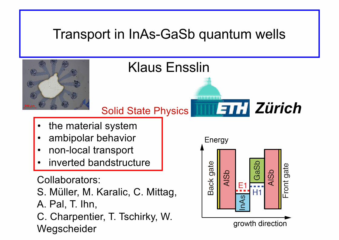
Transport in InAs-GaSb quantum wells
Klaus Ensslin
Solid State Physics• the material system• ambipolar behavior• non-local transport• inverted bandstructure
Zürich
Collaborators:S. Müller, M. Karalic, C. Mittag, A. Pal, T. Ihn, C. Charpentier, T. Tschirky, W. Wegscheider
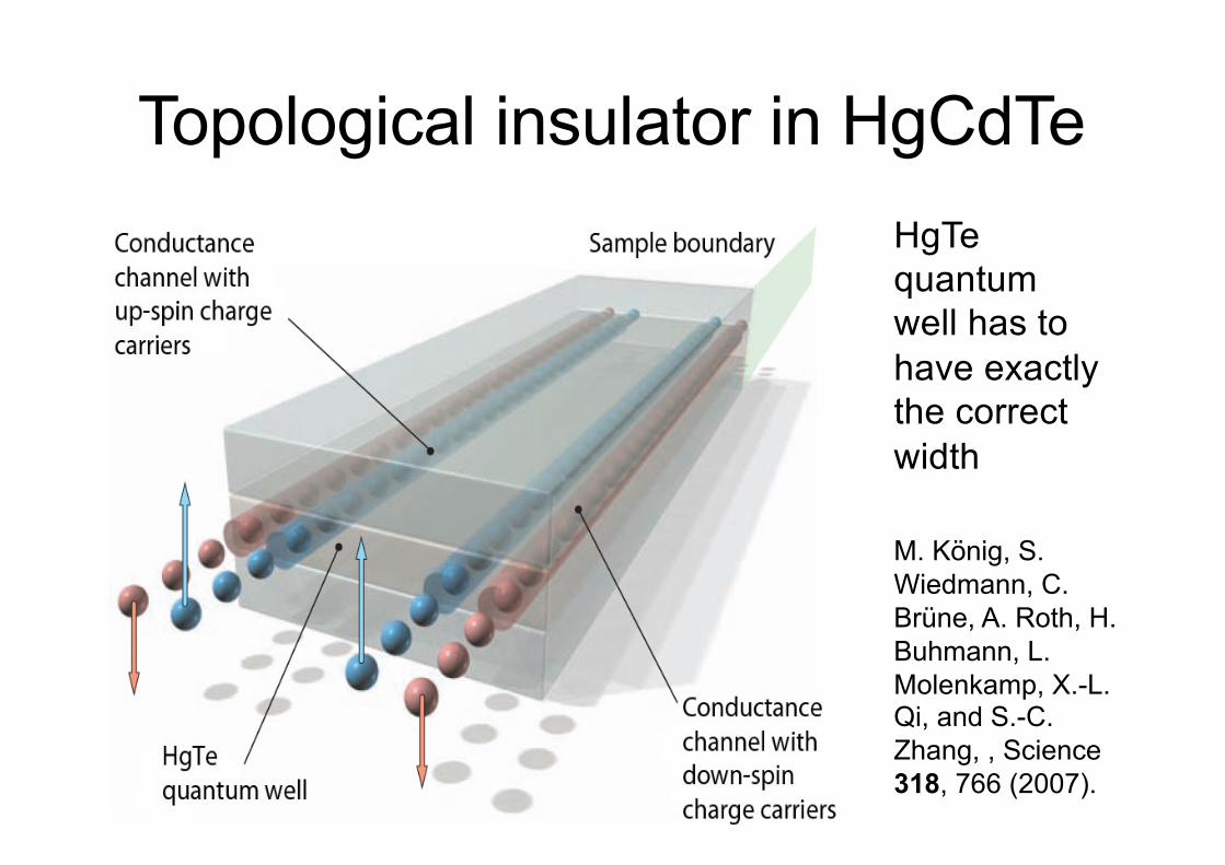
Topological insulator in HgCdTe
M. König, S. Wiedmann, C. Brüne, A. Roth, H. Buhmann, L. Molenkamp, X.-L. Qi, and S.-C. Zhang, , Science 318, 766 (2007).
HgTequantum well has to have exactly the correct width
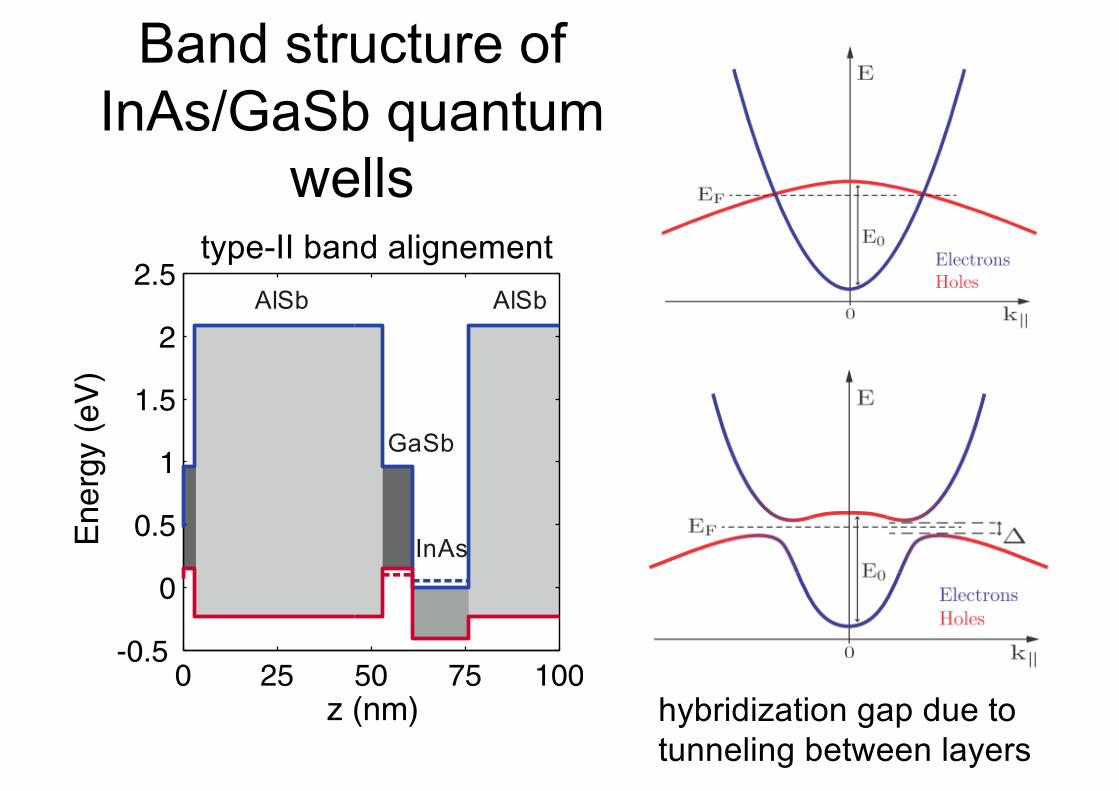
Band structure ofInAs/GaSb quantum
wells
InAs
GaSb
AlSb AlSb
type-II band alignement
hybridization gap due to tunneling between layers
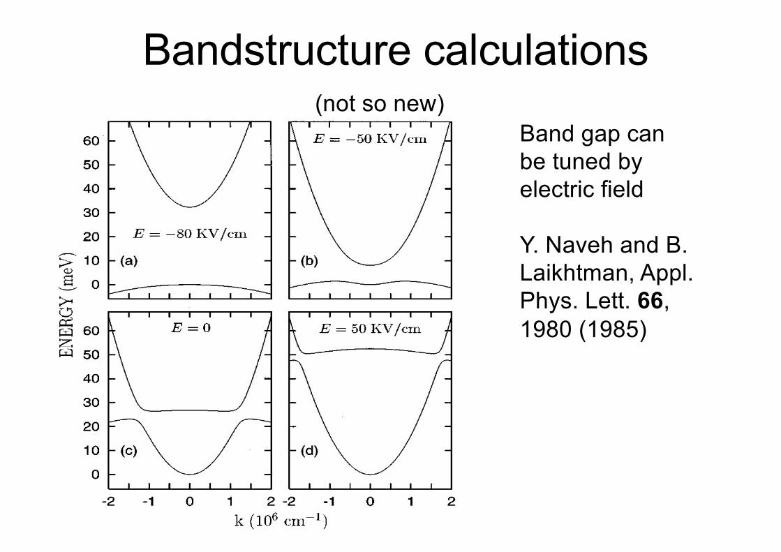
Y. Naveh and B. Laikhtman, Appl. Phys. Lett. 66, 1980 (1985)
Band gap can be tuned by electric field
(not so new)
Bandstructure calculations
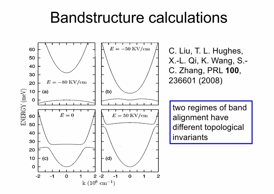
Bandstructure calculations
C. Liu, T. L. Hughes, X.-L. Qi, K. Wang, S.-C. Zhang, PRL 100, 236601 (2008)
two regimes of band alignment have different topological invariants
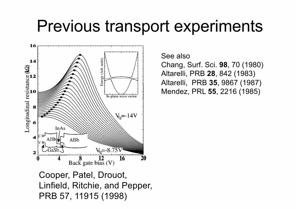
Cooper, Patel, Drouot, Linfield, Ritchie, and Pepper, PRB 57, 11915 (1998)
See alsoChang, Surf. Sci. 98, 70 (1980)Altarelli, PRB 28, 842 (1983)Altarelli, PRB 35, 9867 (1987)Mendez, PRL 55, 2216 (1985)
Previous transport experiments
Previous transport experiments
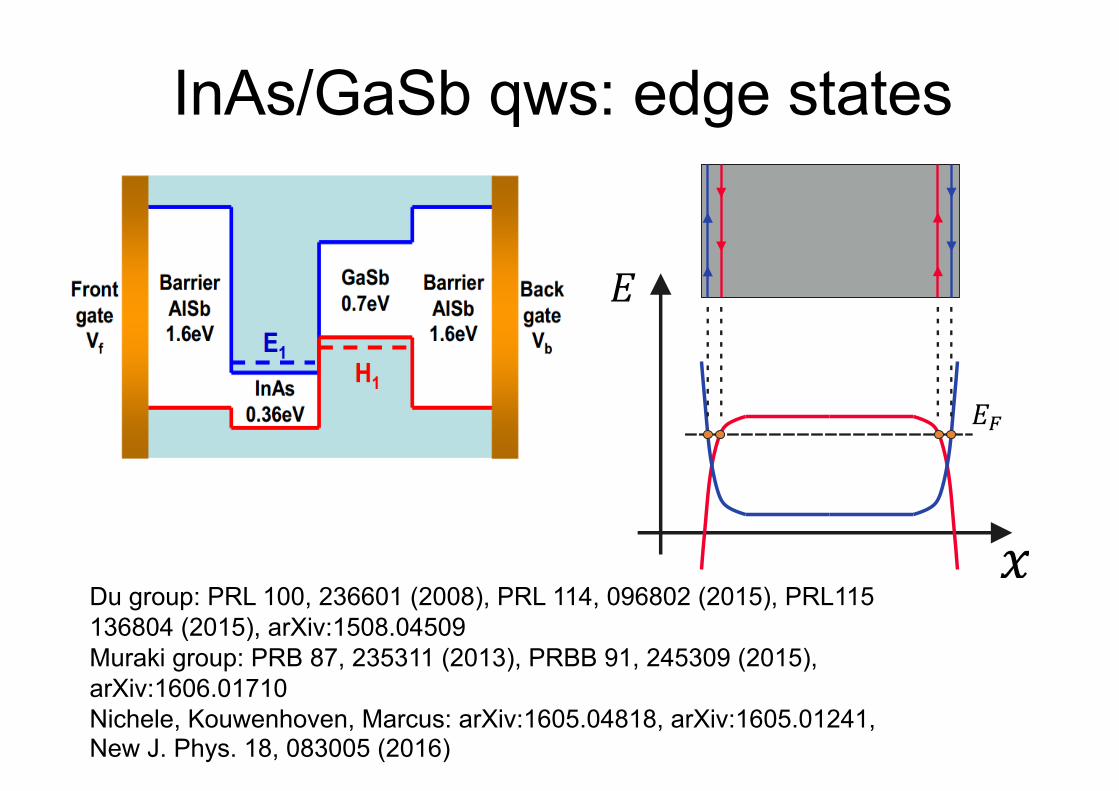
InAs/GaSb qws: edge states
Du group: PRL 100, 236601 (2008), PRL 114, 096802 (2015), PRL115 136804 (2015), arXiv:1508.04509Muraki group: PRB 87, 235311 (2013), PRBB 91, 245309 (2015), arXiv:1606.01710Nichele, Kouwenhoven, Marcus: arXiv:1605.04818, arXiv:1605.01241,New J. Phys. 18, 083005 (2016)
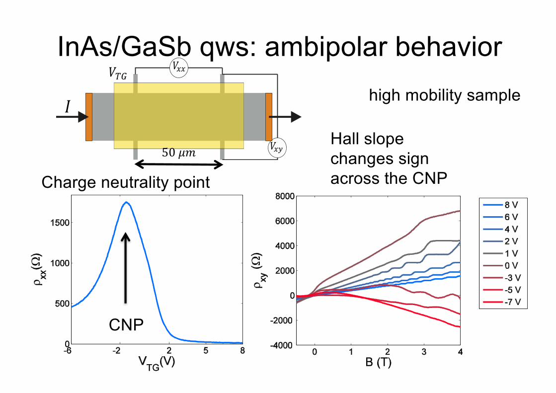
InAs/GaSb qws: ambipolar behavior
50𝜇𝑚
Charge neutrality point
CNP
Hall slopechanges signacross the CNP
high mobility sample
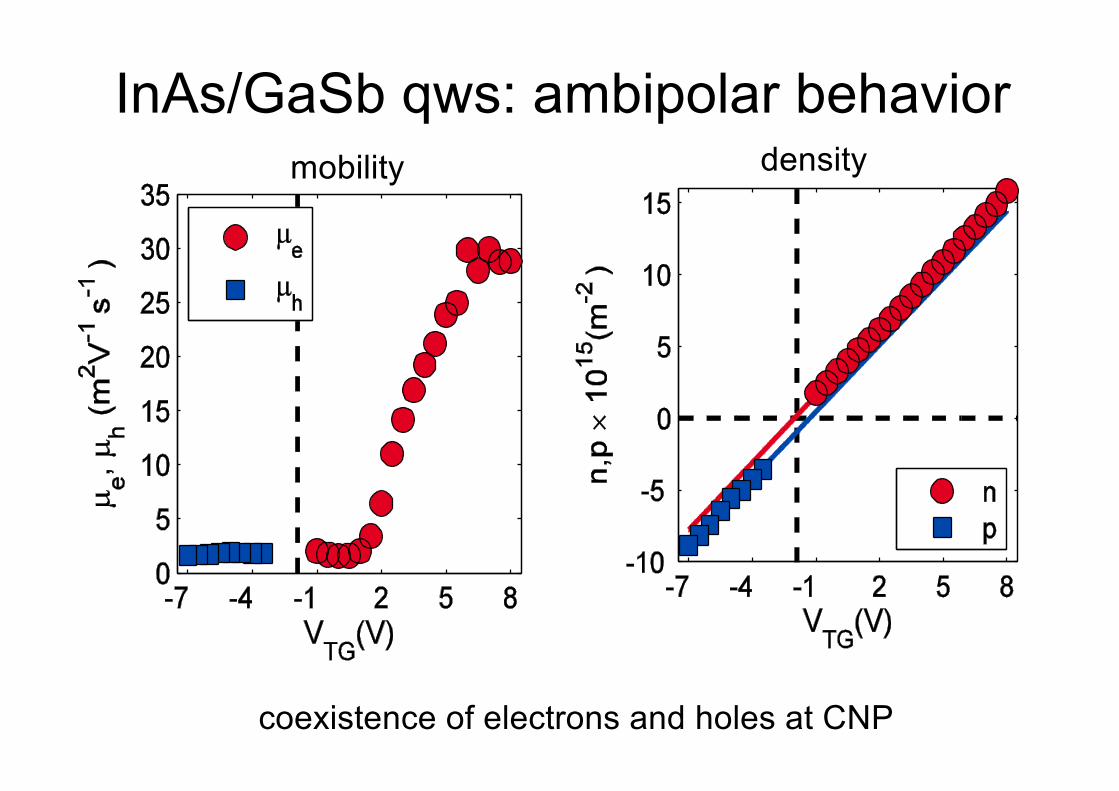
InAs/GaSb qws: ambipolar behaviormobility density
coexistence of electrons and holes at CNP
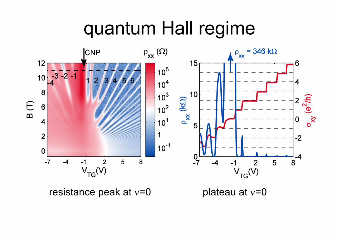
quantum Hall regime
resistance peak at n=0 plateau at n=0
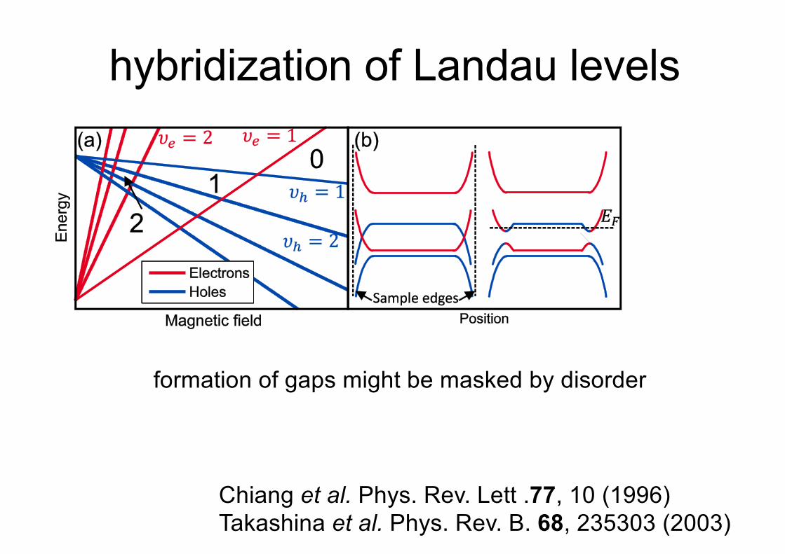
hybridization of Landau levels
Chiang et al. Phys. Rev. Lett .77, 10 (1996)Takashina et al. Phys. Rev. B. 68, 235303 (2003)
formation of gaps might be masked by disorder
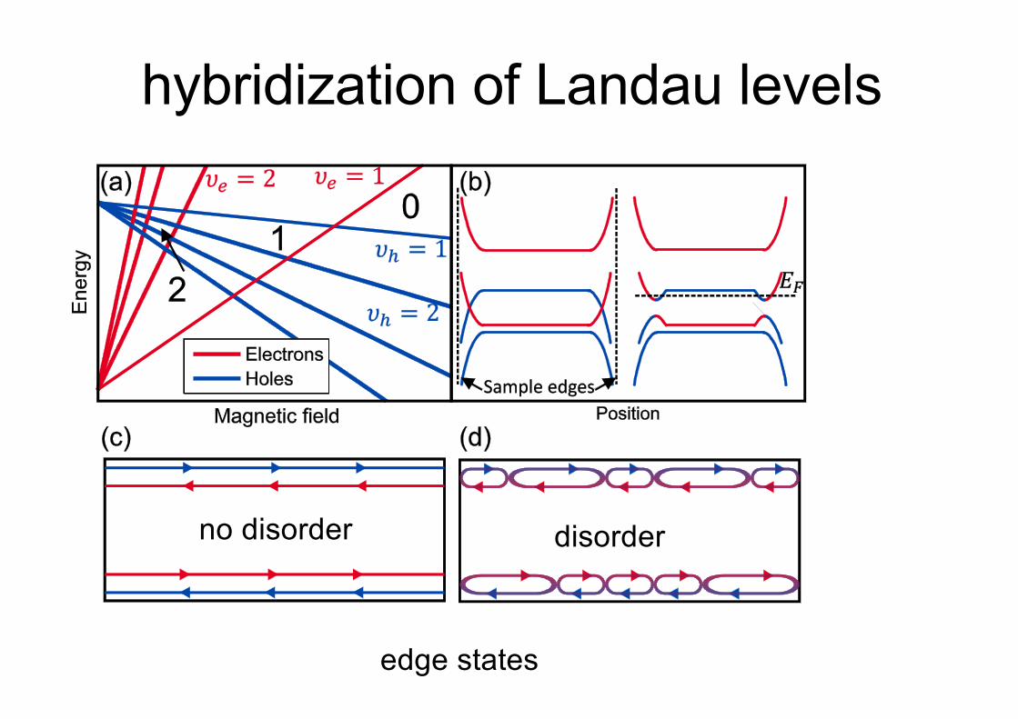
hybridization of Landau levels
edge states
no disorder disorder
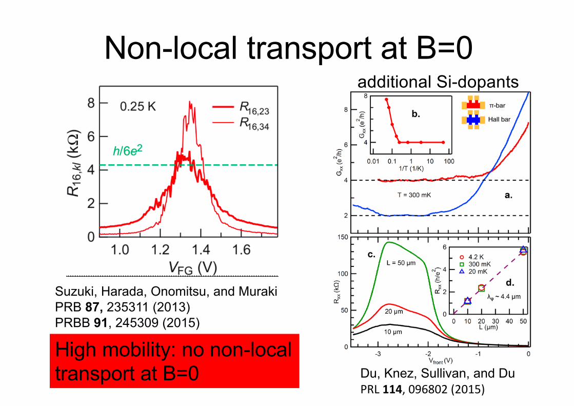
Non-local transport at B=0
10
Figure 2
Suzuki, Harada, Onomitsu, and MurakiPRB 87, 235311 (2013)PRBB 91, 245309 (2015)
Du, Knez, Sullivan, and DuPRL114,096802(2015)
High mobility: no non-local transport at B=0
additional Si-dopants
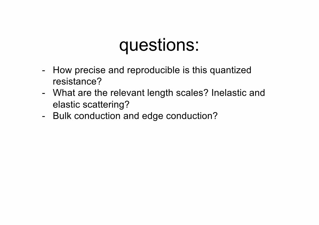
questions:- How precise and reproducible is this quantized
resistance?- What are the relevant length scales? Inelastic and
elastic scattering?- Bulk conduction and edge conduction?
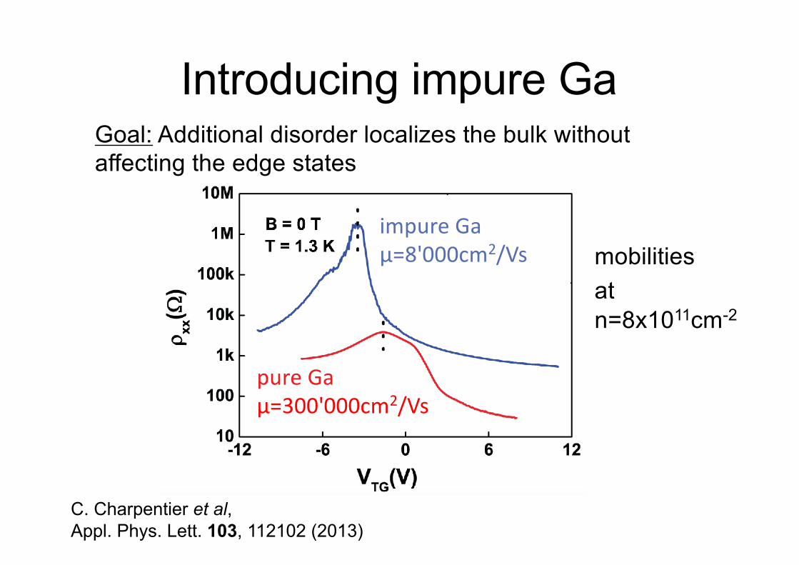
Introducing impure Ga
mobilitiesat n=8x1011cm-2
impureGaμ=8'000cm2/Vs
pureGaμ=300'000cm2/Vs
C. Charpentier et al,Appl. Phys. Lett. 103, 112102 (2013)
Goal: Additional disorder localizes the bulk without affecting the edge states
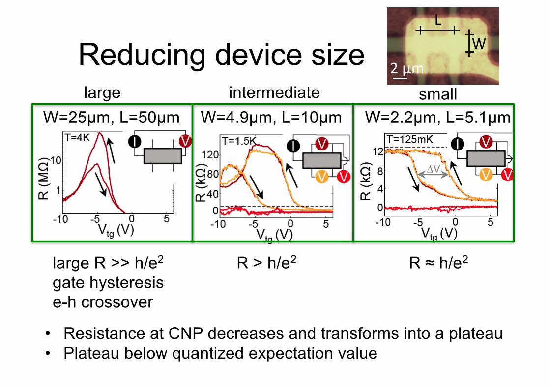
Reducing device size
W=4.9μm, L=10μm W=2.2μm, L=5.1μm
• Resistance at CNP decreases and transforms into a plateau• Plateau below quantized expectation value
LW
2 μm
W=25μm, L=50μm
large R >> h/e2
gate hysteresise-h crossover
R > h/e2
large intermediate
R ≈ h/e2
small
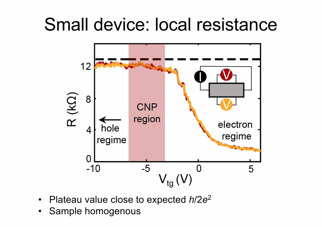
Small device: local resistance
• Plateau value close to expected h/2e2
• Sample homogenous
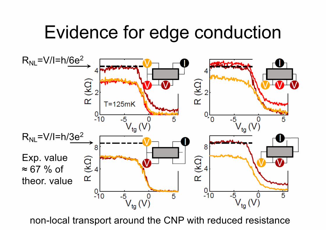
Evidence for edge conductionRNL=V/I=h/6e2
RNL=V/I=h/3e2
non-local transport around the CNP with reduced resistance
Exp. value ≈ 67 % of theor. value
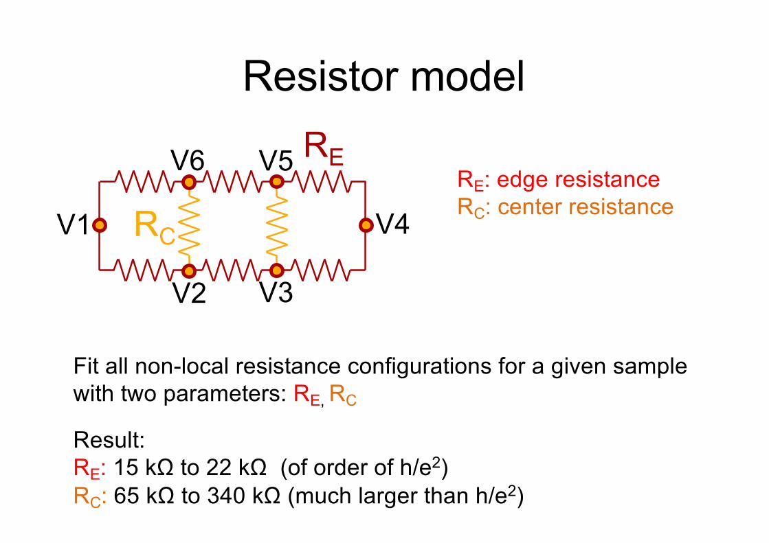
Resistor model
RE: edge resistanceRC: center resistance
4
voltage leads. In general we find that di↵erent contactconfigurations related by the generalized Onsager sym-metry relations [30] always give consistent results, as ex-pected. This reduces the set of independent four-terminalmeasurements in our six-terminal devices to ten, whichclassify into conventional configurations (Fig. 1(e)), non-local resistance configurations (NL-R config.) of type 1(Figs. 2(a,b)), where the current is driven between neigh-boring contacts, and non-local resistance configurationsof type 2 (Figs. 2(c,d)), where the current flows betweennext nearest neighboring contacts.
Additionally, geometric symmetries of the samples(e.g. reflections at the Hall bar axis, or inversions atthe Hall bar center) always gave consistent results. Thisobservation and the vanishing zero magnetic field Hallresistance (see Figs. 1(c,e)) give evidence for a homoge-neous bulk and excellent contact properties witnessingthe high quality of our devices.
Due to the Onsager symmetries the sketched schemat-ics in Fig. 1(e) and Figs. 2(a-c), represent all the possibleconfigurations. In Fig. 1(e) and Fig. 2 the expected quan-tization values for helical edge states of h/2e2 (Fig. 1(e)),h/6e2 (Figs. 2(a,b)) and h/3e2 (Figs. 2(c,d)) are shown asdashed black lines. In all configurations the experimen-tal plateau values are systematically below the expecta-tion. For all voltage drops, which are truly non-local (faraway from the current leads, vanishing local resistancein the electron regime, see Fig. 2(a) red and yellow, andFig. 2(c)), the ratios of plateau values of pairs of di↵er-ent configurations are exactly given by the ratios of theexpected plateau values in an ideal topological insulatorwithout residual bulk conductivity. Device B, for exam-ple, reaches about 66% of the expected plateau valuesin all truly non-local configurations. The mean plateauvalues together with their uncertainties and these scalingfactors are summarized in Table I for all devices and alltypes of configurations. The clear non-local signals to-gether with this consistent scaling are in agreement withthe theoretically proposed current carrying helical statesalong the edge.
Device C has an o↵-centered gate resulting in di↵er-ent gated edge segment lengths Les between consecu-tive contacts. Even though the length of these edge seg-ments varies by a factor of 4, the corresponding non-localplateau resistances remain constant, as shown exemplar-ily in Fig. 3(a) in color for the configuration schemati-cally described in the inset and with black circles for thecorresponding measurements related by symmetry. Thisindependence on edge length excludes trivial edge con-duction characterized by a resistance per length as indi-cated with the black dashed line strongly deviating fromthe measurements. This finding strongly supports thetheoretical expectation of ideal helical edges, but with atoo low plateau resistance value.
The independence of plateau resistances on edge lengthsuggests a resistor network model for the description oftransport in the plateau region of the devices similar asin Ref. 23 consisting of a series of resistors RE along the
V1
V2 V3
V5
V4
REV6
RC
FIG. 3. (a) Value of the non-local four-terminal plateau re-sistance as a function of the edge length Les. Black dashedline: Linear dependence of resistive edge states. (b) Resistornetwork: Here RC symbolizes a residual bulk resistance, RE
the edge-resistance and V1 through V6 the voltage probes.The bar graphs in (c)-(f) allow a comparison of samples Athrough D between the measured four-terminal resistances(filled bars), as schematically shown in the respective top rightcorners, and the calculated prediction with the model (dottedbars).
edge as schematically shown in Fig. 3(b) in red. The ob-served finite bulk conductance is accounted for by addingbulk leakage resistors RC to the model in Fig. 3(b). Al-though this model oversimplifies the real situation it mayserve as a tool to compare the relative relevance of edgeand bulk conduction.One measurement configuration (here the configura-
tion shown in Fig. 2(a)) is su�cient to calculate thetwo unknown resistors in the network model. The re-sult is a bulk coupling RC between 65.4 k⌦ (device D)and 339.5 k⌦ (device A), which is an order of magnitudelarger than the edge-resistance RE ranging from 15.3 k⌦(device D) to 21.9 k⌦ (device A) (for more details seeTable I), confirming the dominant edge conduction andthe model assumption. Even though, RC simplifies thedescription of the bulk contribution, the calculated pre-dictions of all possible measurement configurations basedon the configuration in Fig. 2(a) pass the test of beingcompared with the measurements as illustrated with thebar graphs in Figs. 3(c-f). Our analysis demonstratesthat one set of RE and RC is su�cient to describe allmeasurement configurations.Upon completion we became aware of the manuscript
by Suzuki et al. [31].
Fit all non-local resistance configurations for a given sample with two parameters: RE, RC
Result:RE: 15 kΩ to 22 kΩ (of order of h/e2)RC: 65 kΩ to 340 kΩ (much larger than h/e2)
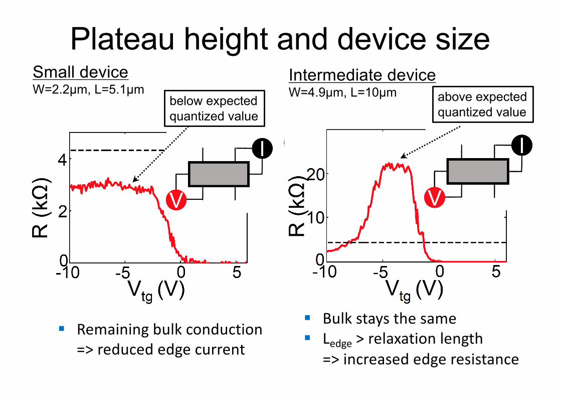
Plateau height and device sizeSmall deviceW=2.2μm, L=5.1μm
Intermediate deviceW=4.9μm, L=10μmbelow expected
quantized valueabove expectedquantized value
§ Remainingbulkconduction=>reducededgecurrent
§ Bulkstaysthesame§ Ledge >relaxationlength
=>increasededgeresistance
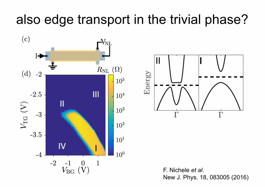
also edge transport in the trivial phase?
F. Nichele et al.New J. Phys. 18, 083005 (2016)
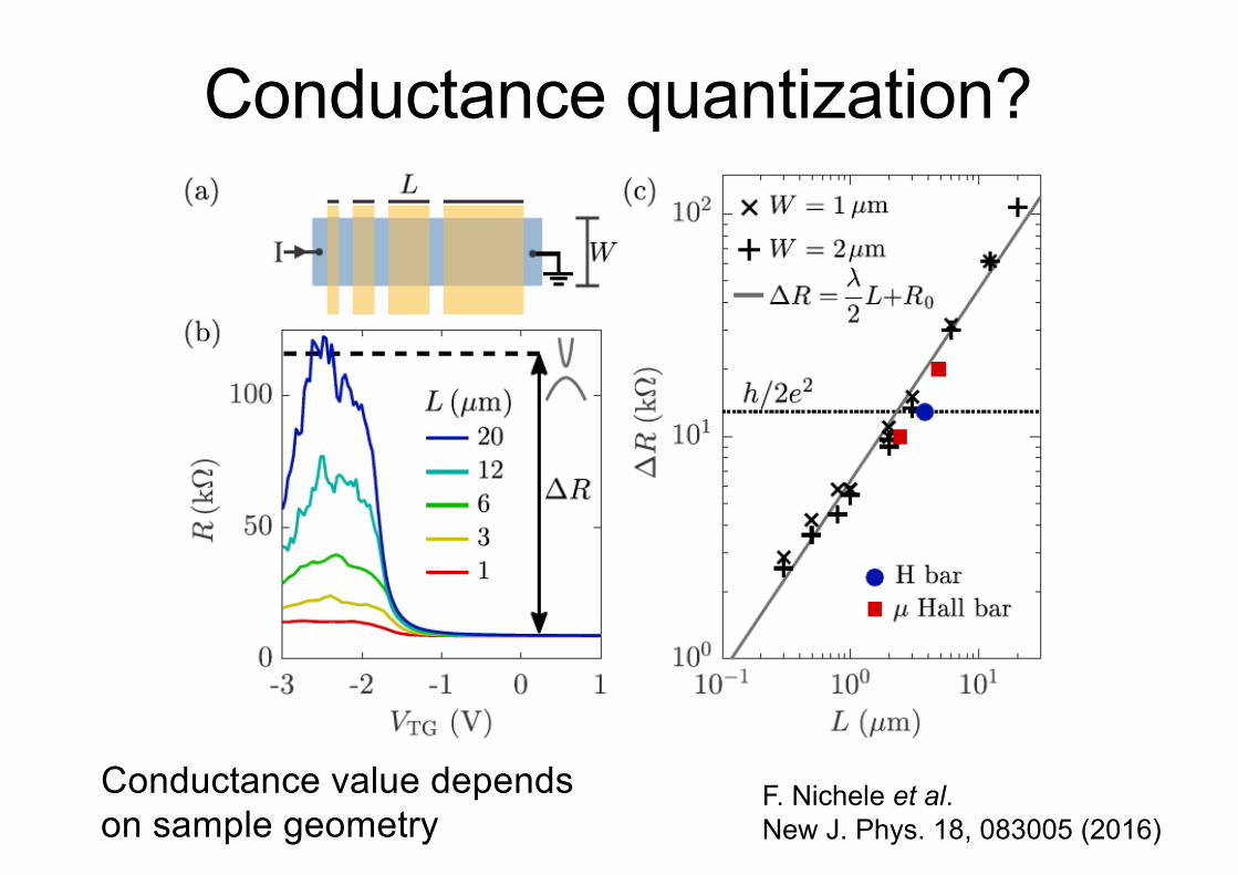
Conductance quantization?
Conductance value depends on sample geometry
F. Nichele et al.New J. Phys. 18, 083005 (2016)
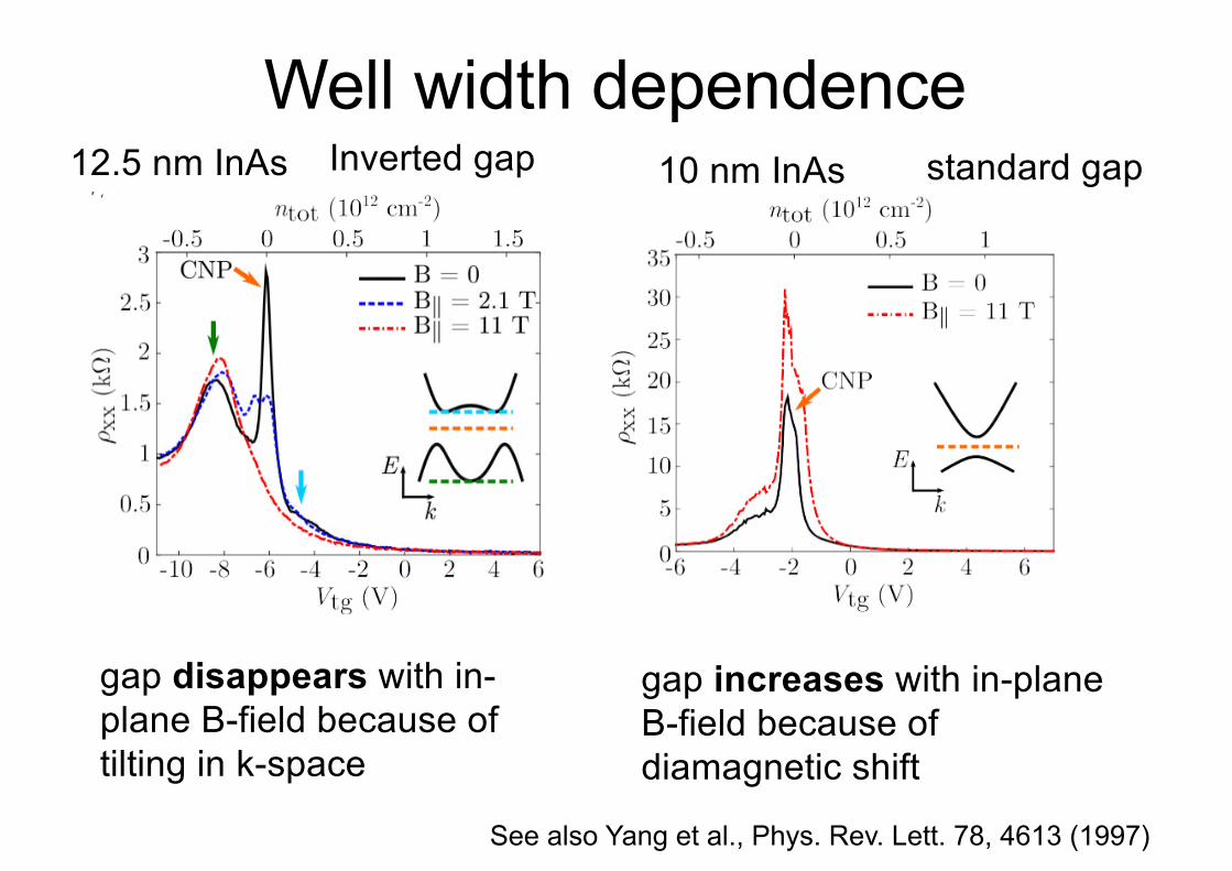
Well width dependence12.5 nm InAs 10 nm InAsInverted gap standard gap
gap disappears with in-plane B-field because of tilting in k-space
gap increases with in-plane B-field because of diamagnetic shift
See also Yang et al., Phys. Rev. Lett. 78, 4613 (1997)
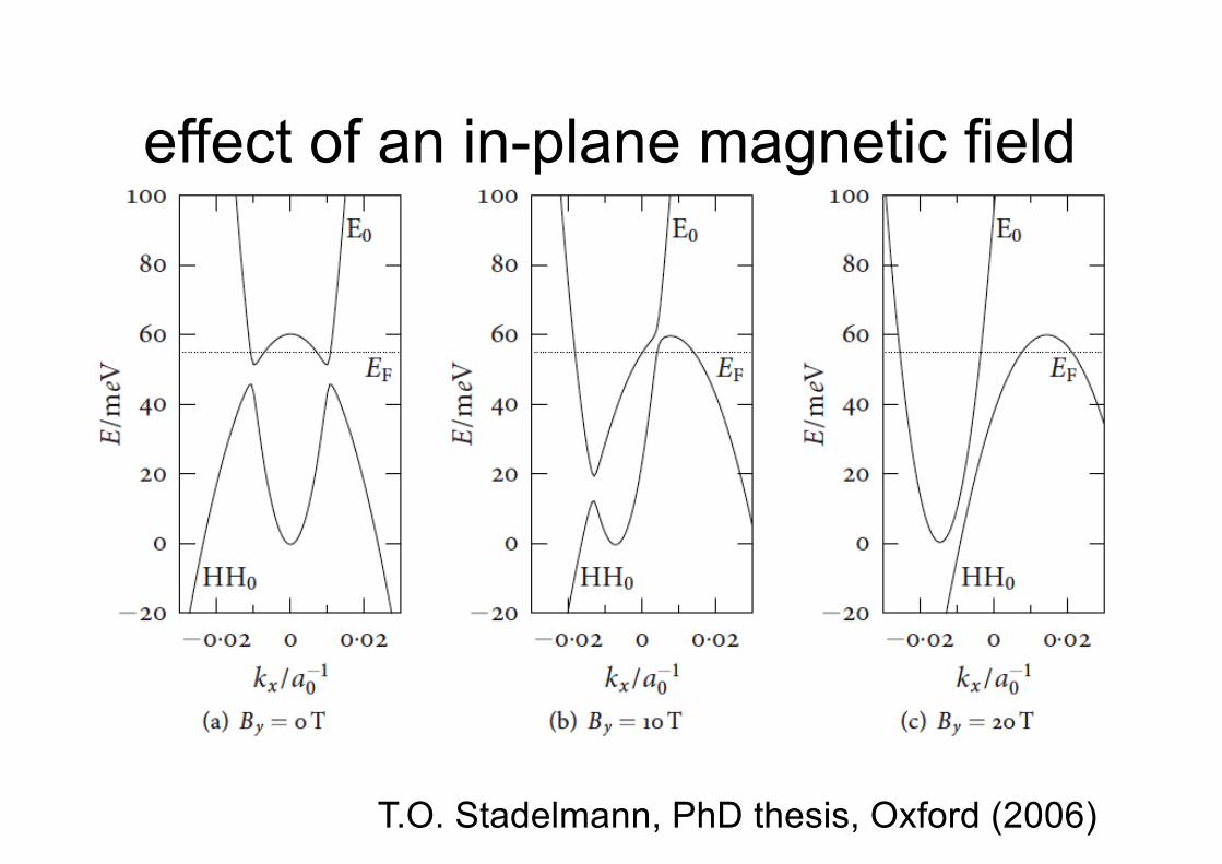
T.O. Stadelmann, PhD thesis, Oxford (2006)
effect of an in-plane magnetic field
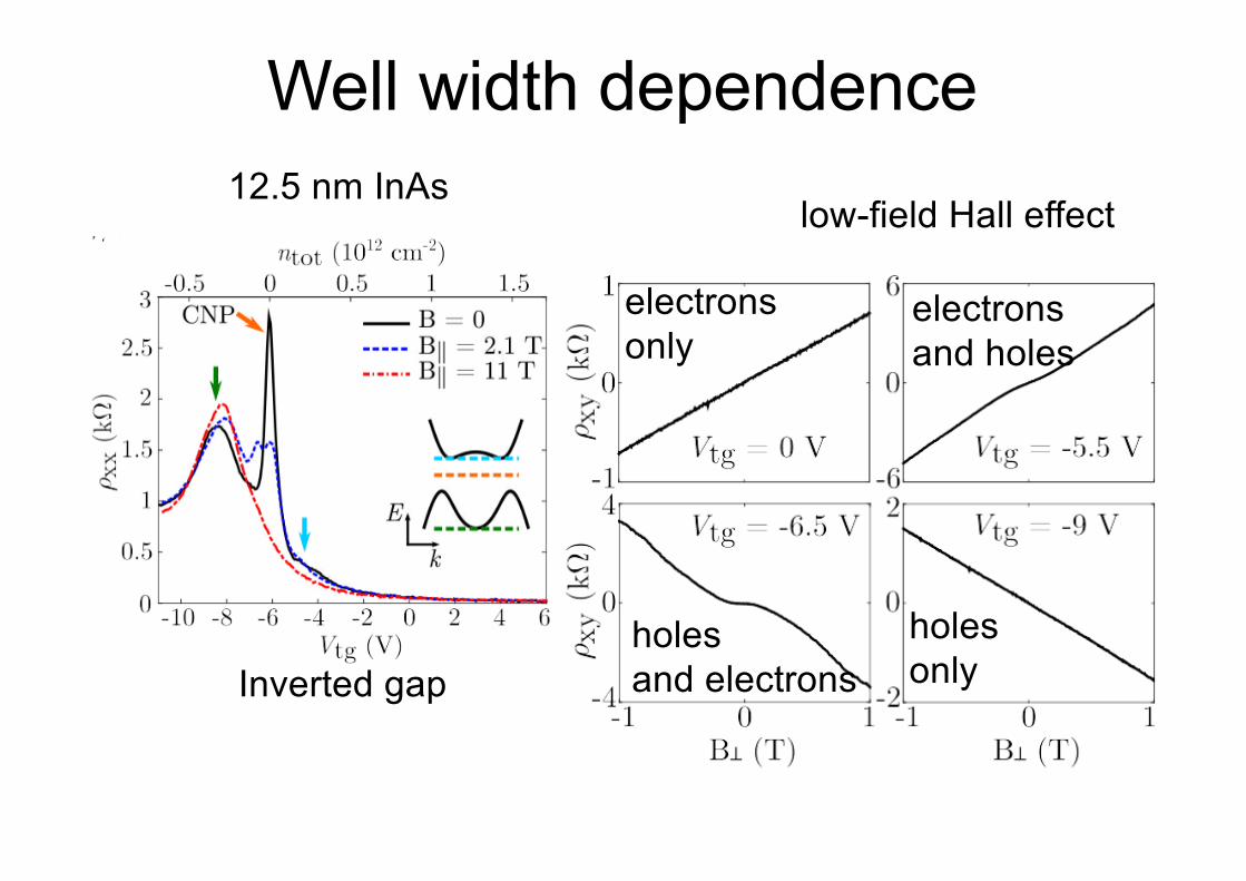
Well width dependence12.5 nm InAs
Inverted gap
low-field Hall effect
electrons only
holes only
electrons and holes
holes and electrons
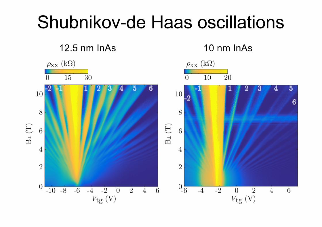
Shubnikov-de Haas oscillations12.5 nm InAs 10 nm InAs
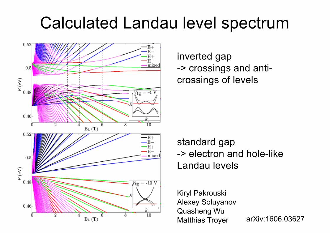
Calculated Landau level spectrum
standard gap-> electron and hole-like Landau levels
inverted gap-> crossings and anti-crossings of levels
arXiv:1606.03627
Kiryl PakrouskiAlexey SoluyanovQuasheng WuMatthias Troyer
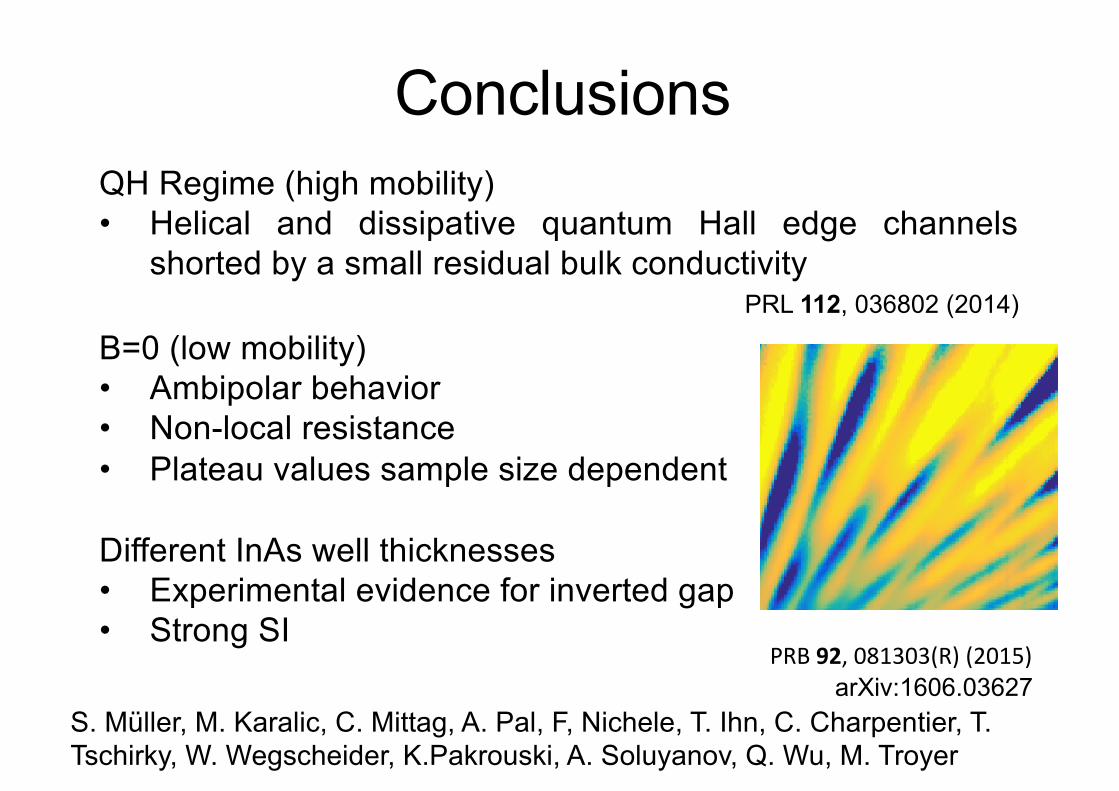
ConclusionsQH Regime (high mobility)• Helical and dissipative quantum Hall edge channels
shorted by a small residual bulk conductivityPRL 112, 036802 (2014)
B=0 (low mobility)• Ambipolar behavior • Non-local resistance• Plateau values sample size dependent
Different InAs well thicknesses• Experimental evidence for inverted gap• Strong SI
S. Müller, M. Karalic, C. Mittag, A. Pal, F, Nichele, T. Ihn, C. Charpentier, T. Tschirky, W. Wegscheider, K.Pakrouski, A. Soluyanov, Q. Wu, M. Troyer
PRB92,081303(R)(2015)arXiv:1606.03627
Thank youThomas Ihn
Susanne Müller
Werner Wegscheider
FabrizioNichele
Atin Pal
Matija Karalic
Christopher MittagThomasTschirky