Embed Size (px)
Citation preview
ORIGINAL PAPER
Transparent conducting zinc oxide as anti-reflection coating depositedby radio frequency magnetron sputtering
R Das1* and S Ray2
1School of Applied Science, Haldia Institute of Technology, Haldia 721657, WB, India
2Energy Research Unit, Indian Association for the Cultivation of Science, Kolkata 700 032, WB, India
Received: 06 July 2010 / Accepted: 09 February 2011 / Published online: 1 March 2012
Abstract: Highly transparent (visible transmission above 90%) and conducting ZnO:Al thin films with strong anti-
reflection property have been prepared by reactive radio frequency (rf) magnetron sputtering under Ar ? H2 ambient,
substrate temperature at 300�C. H2 ratio in the Ar and H2 gas fed from 0 to 40%. The electrical resistivity and sheet
resistance of ZnO:Al film are 2.8 9 10-4ohm-cm and less than 10X/h respectively. The % reflectance (R) is significantly
small (2% [ R [ 0.5%) in the wavelength range 1,000–1,500 nm and the refractive index (n) of the same ZnO:Al film is
1.49 at k = 1,100 nm. All ZnO:Al films have \002[ orientation with good surface topography.
Keywords: Magnetron sputtering; Transparent conducting ZnO:Al thin film; Broadband near infrared anti-reflection
coating; Hydrogen ambient; Telecommunication application
PACS No.: 77.55hf; 78.20.Ci; 78.40.-q
1. Introduction
Reflective and antireflective (AR) optical coatings have
been developed for a variety of applications, e.g., for optical
and electro-optical systems in telecommunications, medi-
cine, military products and consumer products. Now a days
physical vapor deposition (PVD) processes play dominant
role in the fabrication of high quality optical interference
coatings. E-beam evaporation is the preferred deposition
method for large-scale applications. The biggest challenges
are: (i) Identification of a material with suitable refractive
index. (ii) Selection of a stable and volatile precursor spe-
cies allowing the deposition of high quality films with low
absorption, low stress, low surface roughness, good stability
at high humidity, and (iii) High precision thickness control.
AR coatings have been widely used in glass lenses, eye-
glasses, lasers, mirrors, solar cells, IR diodes, multipurpose
broad and narrow band-pass filters, architectural and auto-
motive glass and displays such as cathode ray tubes, as well
as plasma, liquid crystal and flat panel displays [1–5]. Most
common material for a single layer coating is MgF2, which
has relatively low refractive index of 1.38 at visible wave-
length compared to glass. Several workers reported about
the double layer and multilayer coatings such as MgF2–
ZnS, MgF2–TiO2, and SiO2–SiN. Chopra et al. [6] exam-
ined the deposition of ZnSMgF2-SiO, ZnS-Na2AlF, and
GeZnS composite thin films and their multilayers. Belkind
et al. [7] used two tilted planar magnetrons for co-sputtering
some oxides (A12O3–SiO2, Al2O3–TiO2, ZrO2/TiO2) and
nitride TiN–ZrN. Sankur and Gunning [8, 9] used e-beam
deposition to produce mixed TiO2–SiO2, and discussed
changes in the microstructure of the deposited films. Cevro
[10] discussed about Ta2O5–SiO2 composite AR-coating in
near infra-red region. Shivalingappa et al. [11] described
e-beam technique for deposition of CeO2–SiO2 thin films.
Several researchers have worked on transparent con-
ducting ZnO films and reported the material properties for
different applications such as in photo-electronic devices
[12], displays thin film solar cells and recently in the fab-
rication of light emitting diodes [13]. Kluth et al. [14] and
Jin et al. [15] have developed ZnO:Al films suitable for
energy efficient windows of microcrystalline silicon solar
cell and as well as for the application as back reflector for
light trapping in solar cells. No scientific information
regarding anti-reflection properties of ZnO film has been
reported till date.
� 2012 IACS
*Corresponding author, E-mail: [email protected]
Indian J Phys (January 2012) 86(1):23–29
DOI 10.1007/s12648-012-0010-9
In this paper, we report the development of ZnO:Al
films on glass substrate prepared by reactive sputtering
using H2 as reactant gas and its Anti-reflection property in
the specific wavelength region. To prepare aluminium
doped zinc oxide films, rf-Magnetron Sputtering technique
is preferred rather than other chemical vapor deposition
(CVD) methods due to its uniform ion damage free films
over a large area with precise thickness control and high
rate of deposition [16–20]. Detail studies have been done
on the influence of hydrogen ambient on ZnO:Al films
properties. In this paper, attempt has been made to correlate
optical properties of ZnO:Al films with its electrical,
microstructural and surface properties.
2. Experimental details
Aluminium-doped zinc oxide films were deposited on
Corning 7059 glass using an rf-planar magnetron sputtering
system (Nordiko, UK) by both non-reactive and reactive
sputtering under different conditions. A sintered ceramic
disc of ZnO:Al2O3 (2 wt%) was used as the target. During
non-reactive sputtering inert gas like Ar was used in the
deposition chamber. In case of reactive sputtering hydro-
gen gas was incorporated with Ar gas in different propor-
tion as reactant. During each deposition the chamber
pressure was kept constant with the help of a throttle valve
and the gas flows were maintained by mass flow control-
lers. Substrates of Corning 7059 glass were placed parallel
to the target surface at a distance of 7 cm. The rf-power is
applied between two capacitively coupled electrodes.
Before each deposition, the base pressure inside the
deposition unit was brought down to 4 9 10-4 Pa by
water-cooled oil diffusion pump through a liquid nitrogen
trap. ZnO films were deposited at rf-power = 100 Watt,
chamber pressure = 0.4 Pa, and substrate temperature at
300�C.
The film thickness was measured using a surface profi-
lometer. The electrical resistivity of the films was mea-
sured at room temperature by the Van der Pauw method.
The carrier concentration and carrier mobility of the film
were estimated by Hall Effect. A double-beam UV–VIS-
NIR spectrophotometer combined with a photo multiplier
tube (PMT) and a Peltier-cooled PbS IR detector (ISR-
3100 Integrating Sphere with 60 mm diameter was
attached) was used to measure the optical transmittance
and diffuse reflectance spectra of the transparent conduct-
ing oxide (TCO) thin films in the wavelength range 220–
1,800 nm in 1 nm interval with the light beam of 8� angle
of incidence. Refractive indices of the films were measured
by Ellipsometry (J.J.Woollam, USA). The data acquisition
(w and D) versus wavelength in the range 250–1,100 nm
was done for three incident angles 56�, 59� and 62� for
each point. The orientations of the crystallographic planes
as well as the microstructural analysis were investigated by
X-ray diffraction (XRD) (Philips) using monochromatic
Cu–Ka radiation (35 K/20 mA) with wavelength 1.54 A.
The detail study of surface topography was performed by
atomic force microscopy (AFM) measurement using a
NanoScope III instrument with an etched silicon cantilever
having a tip radius of 10 nm and 35� apex angle. Data were
taken in air ambient in tapping mode. Total scans were
extended over areas of 2 9 2 lm. The elemental analysis
was done by energy dispersive spectroscopy (EDS) with
20 kV operating voltage attached with scanning electron
microscope (SEM) (JEOL JSM 6700F).
3. Results and discussions
3.1. Electrical properties
The dependence of electrical resistivities of ZnO:Al films
with rf-power and chamber pressure prepared under dif-
ferent gas ambients have been studied in detail and dis-
cussed elsewhere [21]. The lowest resistivity of ZnO:Al
films prepared at Ar atmosphere was 6.7 9 10-4 ohm-cm
under the optimum deposition condition (rf-power = 100
Watt, chamber pressure = 0.4 Pa, Ar-flow = 50 sccm and
substrate temperature at 300�C). ZnO films were also
prepared under Ar ? H2 plasma with same deposition
conditions using different hydrogen dilution ratio (CH).
The lowest resistivity (q) and sheet resistance (Rsh) of ZnO
film prepared under Ar ? H2 ambients were 2.8 9 10-4
ohm-cm and 6.8X/h respectively. It is interesting to note
that initially with increase of hydrogen dilution in the
deposition chamber, the resistivity of ZnO films decreases
and then increases with further increase of CH (CH = [H2/
(Ar ? H2)] 9 100%). Here the film thicknesses of ZnO
films are lying between 800 nm to 900 nm.
The carrier concentration of different ZnO films as
estimated from Hall effect measurements, varies from
4.8 9 1018 to 2.3 9 1021 cm-3 as the films were prepared
under Ar and Ar ? H2 ambients deposited under optimum
conditions. The Hall mobility of the films also decreases
from 23.9 to 8.5 cm2/V.s. The values of electrical param-
eters are shown in Table 1 and discussed below. The
decrease of the resistivity of ZnO:Al film when prepared
with CH B 10% may be consistent with hydrogen remov-
ing oxygen and thereby increasing the zinc–oxygen ratio in
the deposited films. These results in the formation of either
oxygen vacancies or interstitial zinc giving rise to donor
levels [22]. Oxygen vacancies are deep donors in ZnO and
should therefore not contribute significantly to the carrier
concentration. An alternative intrinsic donor is interstitial
zinc, which is a shallow donor but has higher formation
24 R. Das, S. Ray
energy than oxygen vacancies [23], which may increase the
carrier concentration. Therefore, the increase of carrier
concentration into the ZnO film may be attributed due to
incorporation of hydrogen, which is shallow donor level
and used for high n-type doping of ZnO [24]. Hydrogen
behaviors on ZnO as a donor have been reported by several
experimentalists [25–27]. Webb et al. [28] achieved higher
conductivity in sputtered zinc oxide films by introducing
hydrogen into the argon sputter gas. They observed that the
resistivity initially decreases with increasing added
hydrogen up to some optimum condition and then starts
increasing in higher hydrogen partial pressure. Here, it has
been observed from the experimental results that the ZnO
film deposited with higher CH [ 10% values, becomes
more resistive and growth rate becomes slower due to
simultaneous plasma etching during deposition. The
increase in resistivity beyond CH = 10% is due to decrease
in carrier concentration. Hydrogen may act as an ampho-
teric impurity in high hydrogen partial pressure incorpo-
rating as H- (an acceptor) in ZnO:Al film [24]. As a result,
ZnO:Al films deposited at higher CH values may show
increased compensation from an increase in the density of
acceptor levels resulting from changes in the growth
characteristics [29] and hence increases the resistivity.
3.2. Surface properties and elemental analysis
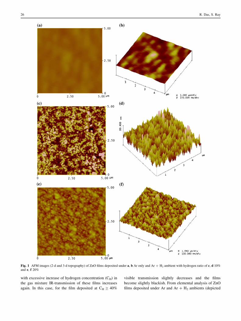
Figure 1a–f presents AFM images showing the 2d- and 3d
topography of ZnO films deposited under Ar and Ar ? H2
ambients.. Clearly the Ar ? H2 deposited ZnO film is
much rougher than the Ar deposited ZnO film.
Quantitative measurements of the root mean square
roughness values have been listed in Table 1. The mini-
mum and maximum values of surface roughness are 2.30
and 9.96 nm, respectively, for Ar and Ar ? H2 deposited
ZnO films. Significant variations in surface feature of dif-
ferent ZnO films are evident from the micrograph. With
incorporation of H2 in Ar as sputtering gas surface
roughness of ZnO films gradually increases to 9.96 nm but
with gradual increase of hydrogen dilution in deposition
chamber, the film growth rate decreases.
Elemental analysis of ZnO films deposited under Ar and
Ar ? H2 ambients, studied by EDS attached with SEM, are
shown in Table 2. The data acquisition has been done for 7
different spots/sample for 2.5 min of each spots. The
results for different spots are almost equivalent for a par-
ticular sample. There is a large increase of the Zn–O ratio
with increasing H2 content.
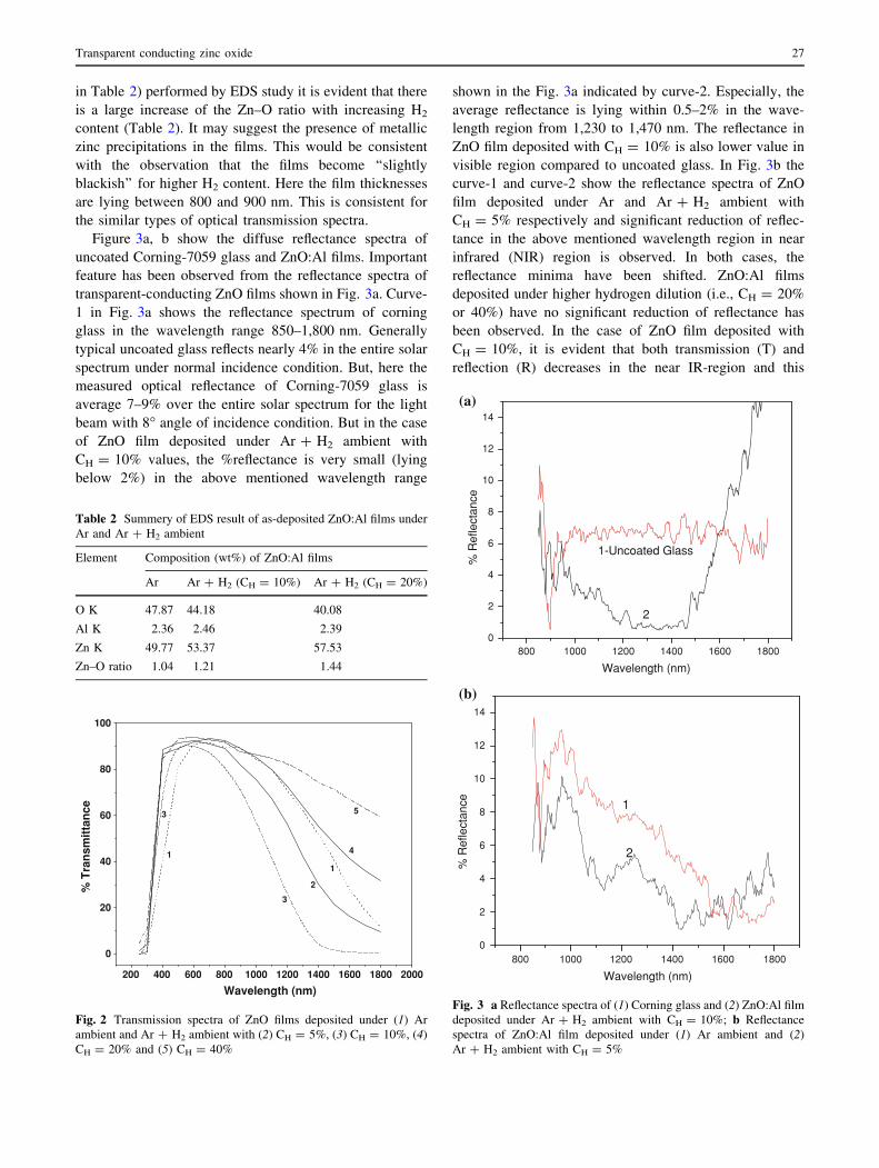
3.3. Optical properties
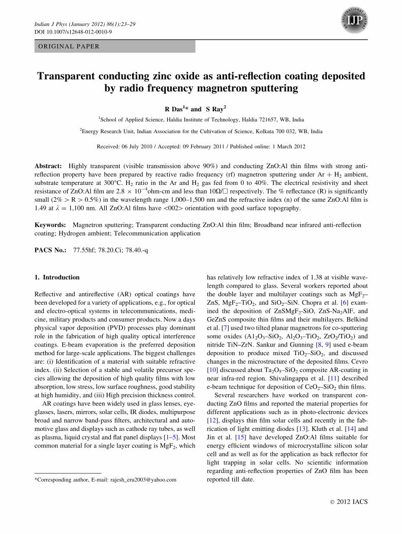
Optical transmittance and reflectance spectra of ZnO:Al
films deposited under Ar, and Ar ? H2 ambients are dis-
played in Figs. 2 and 3a, b, respectively. The average
transmittance of all ZnO:Al films in the visible range is
found to be above 90% shown in Fig. 2. Curve-1 shows the
optical transmittance of ZnO film deposited under Ar
ambient. Curve-2 shows the transmittance curve of the
ZnO film deposited with CH = 5% and here the transmis-
sion peak maxima has shifted towards shorter wavelength
side. For the ZnO film deposited with CH = 10% values
the whole spectrum (Curve-3) is shifted towards shorter
wavelength side. All the ZnO films provides an excellent
UV shielding as the absorption edge in the lower wave-
length side is at k = 300 nm. Important thing is that the
band gap absorption edge has been shifted towards lower
wavelength side for ZnO:Al films deposited under
Ar ? H2 ambient. In the longer wavelength side the
transmission of ZnO:Al films are different for different
films deposited under different conditions. In the case of
ZnO:Al film deposited with CH = 10%, the percentage
transmission is negligible at 1,400 nm compared to 60%
transmission at the same wavelength in case of Ar depos-
ited ZnO film. It is evident that initially the transmission in
IR-region decreases with the increase of CH value, but with
further increase of CH values the % transmission increases
in IR-range. At very low hydrogen dilution i.e. at
CH B 5%, carrier generation increases in the ZnO film but
not too high. On the other hand, it has been observed that
Table 1 The electrical, optical parameter and surface roughness of ZnO:Al films prepared under Ar and Ar ? H2 with different dilution ratio at
300�C
Sputtering
gas ambient
Film resistivity
Ohm-cm
Hall mobility
(l) (cm2/V.s)
Carrier concentration
ne (cm3)
Refractive index at Surface roughness
(nm) drms (nm)500 nm 1,100 nm
Ar 6.7 9 10-4 23.9 3.9 9 1020 1.46 1.71 2.28
Ar ? H2 with different hydrogen dilution (CH = [H2/(Ar ? H2)] 9 100%)
CH = 5 5.5 9 10-4 13.4 6.3 9 1020 1.45 1.52 6.75
CH = 10 2.8 9 10-4 9.7 2.3 9 1021 1.39 1.49 8.26
CH = 20 8.3 9 10-3 9.3 5.3 9 1019 1.48 1.47 9.24
CH = 40 6.7 9 10-2 8.5 4.8 9 1018 1.49 1.46 9.96
Transparent conducting zinc oxide 25
with excessive increase of hydrogen concentration (CH) in
the gas mixture IR-transmission of these films increases
again. In this case, for the film deposited at CH C 40%
visible transmission slightly decreases and the films
become slightly blackish. From elemental analysis of ZnO
films deposited under Ar and Ar ? H2 ambients (depicted
Fig. 1 AFM images (2-d and 3-d topography) of ZnO films deposited under a, b Ar only and Ar ? H2 ambient with hydrogen ratio of c, d 10%
and e, f 20%
26 R. Das, S. Ray
in Table 2) performed by EDS study it is evident that there
is a large increase of the Zn–O ratio with increasing H2
content (Table 2). It may suggest the presence of metallic
zinc precipitations in the films. This would be consistent
with the observation that the films become ‘‘slightly
blackish’’ for higher H2 content. Here the film thicknesses
are lying between 800 and 900 nm. This is consistent for
the similar types of optical transmission spectra.
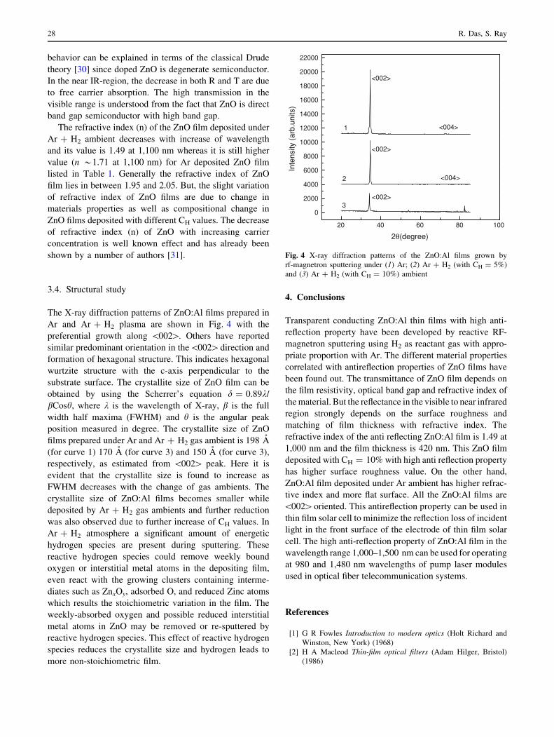
Figure 3a, b show the diffuse reflectance spectra of
uncoated Corning-7059 glass and ZnO:Al films. Important
feature has been observed from the reflectance spectra of
transparent-conducting ZnO films shown in Fig. 3a. Curve-
1 in Fig. 3a shows the reflectance spectrum of corning
glass in the wavelength range 850–1,800 nm. Generally
typical uncoated glass reflects nearly 4% in the entire solar
spectrum under normal incidence condition. But, here the
measured optical reflectance of Corning-7059 glass is
average 7–9% over the entire solar spectrum for the light
beam with 8� angle of incidence condition. But in the case
of ZnO film deposited under Ar ? H2 ambient with
CH = 10% values, the %reflectance is very small (lying
below 2%) in the above mentioned wavelength range
shown in the Fig. 3a indicated by curve-2. Especially, the
average reflectance is lying within 0.5–2% in the wave-
length region from 1,230 to 1,470 nm. The reflectance in
ZnO film deposited with CH = 10% is also lower value in
visible region compared to uncoated glass. In Fig. 3b the
curve-1 and curve-2 show the reflectance spectra of ZnO
film deposited under Ar and Ar ? H2 ambient with
CH = 5% respectively and significant reduction of reflec-
tance in the above mentioned wavelength region in near
infrared (NIR) region is observed. In both cases, the
reflectance minima have been shifted. ZnO:Al films
deposited under higher hydrogen dilution (i.e., CH = 20%
or 40%) have no significant reduction of reflectance has
been observed. In the case of ZnO film deposited with
CH = 10%, it is evident that both transmission (T) and
reflection (R) decreases in the near IR-region and this
Table 2 Summery of EDS result of as-deposited ZnO:Al films under
Ar and Ar ? H2 ambient
Element Composition (wt%) of ZnO:Al films
Ar Ar ? H2 (CH = 10%) Ar ? H2 (CH = 20%)
O K 47.87 44.18 40.08
Al K 2.36 2.46 2.39
Zn K 49.77 53.37 57.53
Zn–O ratio 1.04 1.21 1.44
200 400 600 800 1000 1200 1400 1600 1800 2000
0
20
40
60
80
100
3
1
5
4
3
2
1
% T
ran
smit
tan
ce
Wavelength (nm)
Fig. 2 Transmission spectra of ZnO films deposited under (1) Ar
ambient and Ar ? H2 ambient with (2) CH = 5%, (3) CH = 10%, (4)
CH = 20% and (5) CH = 40%
800 1000 1200 1400 1600 18000
2
4
6
8
(b)
(a)
10
12
14
2
1-Uncoated Glass
% R
efle
ctan
ce
Wavelength (nm)
800 1000 1200 1400 1600 1800
Wavelength (nm)
0
2
4
6
8
10
12
14
2
1
% R
efle
ctan
ce
Fig. 3 a Reflectance spectra of (1) Corning glass and (2) ZnO:Al film
deposited under Ar ? H2 ambient with CH = 10%; b Reflectance
spectra of ZnO:Al film deposited under (1) Ar ambient and (2)
Ar ? H2 ambient with CH = 5%
Transparent conducting zinc oxide 27
behavior can be explained in terms of the classical Drude
theory [30] since doped ZnO is degenerate semiconductor.
In the near IR-region, the decrease in both R and T are due
to free carrier absorption. The high transmission in the
visible range is understood from the fact that ZnO is direct
band gap semiconductor with high band gap.
The refractive index (n) of the ZnO film deposited under
Ar ? H2 ambient decreases with increase of wavelength
and its value is 1.49 at 1,100 nm whereas it is still higher
value (n *1.71 at 1,100 nm) for Ar deposited ZnO film
listed in Table 1. Generally the refractive index of ZnO
film lies in between 1.95 and 2.05. But, the slight variation
of refractive index of ZnO films are due to change in
materials properties as well as compositional change in
ZnO films deposited with different CH values. The decrease
of refractive index (n) of ZnO with increasing carrier
concentration is well known effect and has already been
shown by a number of authors [31].
3.4. Structural study
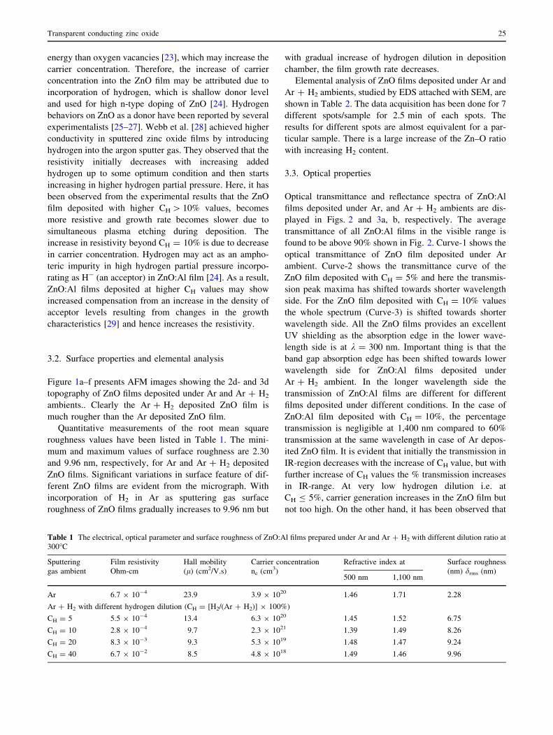
The X-ray diffraction patterns of ZnO:Al films prepared in
Ar and Ar ? H2 plasma are shown in Fig. 4 with the
preferential growth along \002[. Others have reported
similar predominant orientation in the\002[direction and
formation of hexagonal structure. This indicates hexagonal
wurtzite structure with the c-axis perpendicular to the
substrate surface. The crystallite size of ZnO film can be
obtained by using the Scherrer’s equation d = 0.89k/
bCosh, where k is the wavelength of X-ray, b is the full
width half maxima (FWHM) and h is the angular peak
position measured in degree. The crystallite size of ZnO
films prepared under Ar and Ar ? H2 gas ambient is 198 A
(for curve 1) 170 A (for curve 3) and 150 A (for curve 3),
respectively, as estimated from \002[ peak. Here it is
evident that the crystallite size is found to increase as
FWHM decreases with the change of gas ambients. The
crystallite size of ZnO:Al films becomes smaller while
deposited by Ar ? H2 gas ambients and further reduction
was also observed due to further increase of CH values. In
Ar ? H2 atmosphere a significant amount of energetic
hydrogen species are present during sputtering. These
reactive hydrogen species could remove weekly bound
oxygen or interstitial metal atoms in the depositing film,
even react with the growing clusters containing interme-
diates such as ZnxOy, adsorbed O, and reduced Zinc atoms
which results the stoichiometric variation in the film. The
weekly-absorbed oxygen and possible reduced interstitial
metal atoms in ZnO may be removed or re-sputtered by
reactive hydrogen species. This effect of reactive hydrogen
species reduces the crystallite size and hydrogen leads to
more non-stoichiometric film.
4. Conclusions
Transparent conducting ZnO:Al thin films with high anti-
reflection property have been developed by reactive RF-
magnetron sputtering using H2 as reactant gas with appro-
priate proportion with Ar. The different material properties
correlated with antireflection properties of ZnO films have
been found out. The transmittance of ZnO film depends on
the film resistivity, optical band gap and refractive index of
the material. But the reflectance in the visible to near infrared
region strongly depends on the surface roughness and
matching of film thickness with refractive index. The
refractive index of the anti reflecting ZnO:Al film is 1.49 at
1,000 nm and the film thickness is 420 nm. This ZnO film
deposited with CH = 10% with high anti reflection property
has higher surface roughness value. On the other hand,
ZnO:Al film deposited under Ar ambient has higher refrac-
tive index and more flat surface. All the ZnO:Al films are
\002[oriented. This antireflection property can be used in
thin film solar cell to minimize the reflection loss of incident
light in the front surface of the electrode of thin film solar
cell. The high anti-reflection property of ZnO:Al film in the
wavelength range 1,000–1,500 nm can be used for operating
at 980 and 1,480 nm wavelengths of pump laser modules
used in optical fiber telecommunication systems.
References
[1] G R Fowles Introduction to modern optics (Holt Richard and
Winston, New York) (1968)
[2] H A Macleod Thin-film optical filters (Adam Hilger, Bristol)
(1986)
20 40 60 80 100
0
2000
4000
6000
8000
10000
12000
14000
16000
18000
20000
22000
3
2
1
<004>
<004>
<002>
<002>
<002>
Inte
nsity
(ar
b.un
its)
2θ(degree)
Fig. 4 X-ray diffraction patterns of the ZnO:Al films grown by
rf-magnetron sputtering under (1) Ar; (2) Ar ? H2 (with CH = 5%)
and (3) Ar ? H2 (with CH = 10%) ambient
28 R. Das, S. Ray
[3] D Pekker and L Pekker Thin Solid Films 425 203 (2003)
[4] P Nubile Thin Solid Films 342 257 (1999)
[5] H G Shanbhogue, C L Nagendra, M N Annapurna and S A
Kumar Appl. Opt. 36 6339 (1997)
[6] K L Chopra, S K Sharma and V N Yadava Thin Solid Films 20209 (1974)
[7] A Belkind, R Laird, Z Orban and P White Rafalko Thin SolidFilms 219 (1–2), 46 (1992)
[8] H Sankur and W J Gunning J. Appl. Phys. 66 4747 (1989)
[9] N S Cluck, H Sankur, J Heuer, J DeNatale and W J Gunning
J. Appl. Phys. 69 3037 (1991)
[10] M Cevro Thin Solid Films 258 91 (1995)
[11] L Shivalingappa, K N Rao and S Mohan Vacuum 44 1031
(1993)
[12] R-Y Tsai and M-Y Hua Appl. Opt. 35(25) 5073 (1996)
[13] J Cho, J Nah, M-S Oh, J-H Song, K-H Yoon, H-Jin Jung and W-
K Choi Jpn. J. Appl. Phys. 40 L1040 (2001)
[14] O Kluth, B Rech, L Houben, S Wieder, H Wagner, A Loffl and
HW Schock Thin Solid Films 351 247 (1999)
[15] Z-C Jin, I Hamberg and C G Granqvist Appl. Phys. Lett. 51 149
(1987)
[16] B Saha, R Thapa, NS Das and KK Chattopadhyay, Indian J.Phys. 84 681 (2010)
[17] J Lee, T Tanaka, S Sasaki and S Uchiyama J. LightwaveTechnol. 16 884 (1998)
[18] B Saha, R Thapa, S Jana and KK Chattopadhyay Indian J. Phys.84 1341 (2010)
[19] Y Zheng, K Kikuchi, M Yamasaki, K Sonoi and K Uehara
Appl.Opt. 36 6335 (1997)
[20] R Thapa, B Saha, S Goswami and KK Chattopadhyay Indian J.Phys. 84 1347 (2010)
[21] S Ray, R Das and A K Barua Solar Energy Mater Solar Cells 74387 (2002)
[22] W Gopel and U Lampe Phys. Rev. B 22 6447 (1980)
[23] P Erhart, K Albe, and A Klein Phys. Rev. B 73 205203 (2006)
[24] Van de Walle Phys. Rev. Lett. 85 1012 (2000)
[25] E Mollow Z Phys. Chem. Solids 3 87 (1957)
[26] D G Thomas and J J Lander J. Chem. Phys. 25 1136 (1956)
[27] S J Baik, J H Jang, C H Lee, W Y Cho and K S Lim Appl. Phys.Lett. 70 3516 (1997)
[28] J B Webb, D F Williams and M Buchanan Appl. Phys. Lett. 39640 (1981)
[29] W C Mackrodt and R F Stewart J. Physique C 41 6 (1980)
[30] P Drude Z. Phy. D 1 1667 (1968)
[31] H Fujiwara and M Kondo Phys. Rev. B 71 075109 (2005)
Transparent conducting zinc oxide 29