Embed Size (px)
Citation preview
45
Transistor characteristics and approximation
Transistor Static Characteristics:
There are the curves which represents relationship between different d.c. currents
and voltages of a transistor. The three important characteristics of a transistor are:
1. Input characteristic,
2. Output characteristic,
3. Constant-current transfer characteristic.
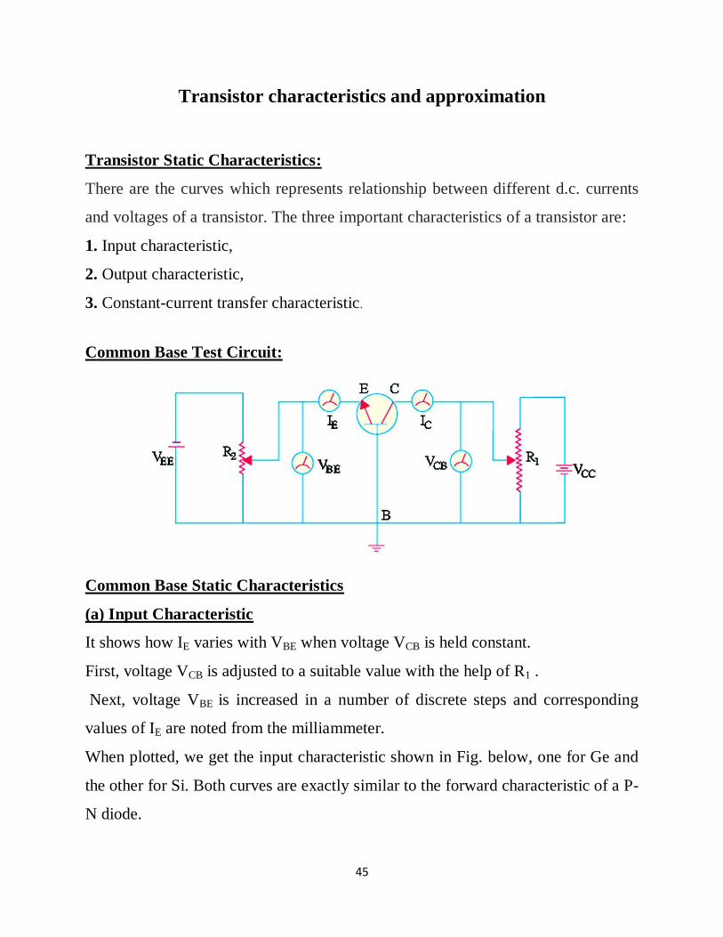
Common Base Test Circuit:
Common Base Static Characteristics
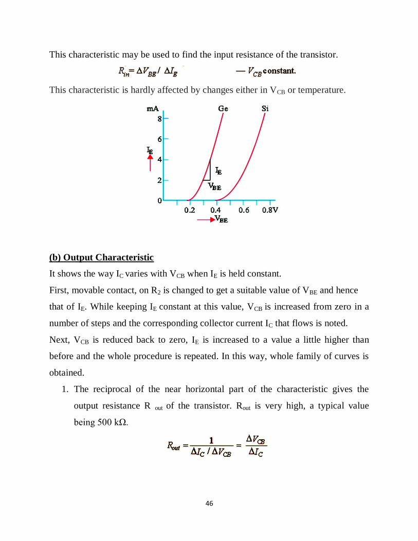
(a) Input Characteristic
It shows how IE varies with VBE when voltage VCB is held constant.
First, voltage VCB is adjusted to a suitable value with the help of R1 .
Next, voltage VBE is increased in a number of discrete steps and corresponding
values of IE are noted from the milliammeter.
When plotted, we get the input characteristic shown in Fig. below, one for Ge and
the other for Si. Both curves are exactly similar to the forward characteristic of a P-
N diode.
46
This characteristic may be used to find the input resistance of the transistor.
This characteristic is hardly affected by changes either in VCB or temperature.
(b) Output Characteristic
It shows the way IC varies with VCB when IE is held constant.
First, movable contact, on R2 is changed to get a suitable value of VBE and hence
that of IE. While keeping IE constant at this value, VCB is increased from zero in a
number of steps and the corresponding collector current IC that flows is noted.
Next, VCB is reduced back to zero, IE is increased to a value a little higher than
before and the whole procedure is repeated. In this way, whole family of curves is
obtained.
1. The reciprocal of the near horizontal part of the characteristic gives the
output resistance R out of the transistor. Rout is very high, a typical value
being 500 kΩ.
47
2. It is seen that IC flows even when VCB = 0. For example, it has a value = 1.8
mA corresponding to VCB = 0 for IE = 2 mA. It is due to the fact that
electrons are being injected into the base under the action of forward-biased
E/B junction and are being collected by the collector due to the action of the
internal junction voltage at the C/B junction. For reducing IC to zero, it is
essential to neutralize this potential barrier by applying a small forward bias
across C/B junction.
3. Another important feature of the characteristic is that a small amount of
collector current flows even when emitter current IE = 0. it is collector
leakage current ICBO.
4. This characteristic may be used to find αac of the transistor.
5. Another point worth noting is that although IC is practically independent of
VCB over the working range of the transistor, yet if VCB is permitted to
increase beyond a certain value, IC eventually increases rapidly due to
avalanche breakdown.
Current Transfer Characteristic
It shows how IC varies with changes in IE when VCB is held constant. For drawing
this characteristic, first VCB is set to a convenient value and then IE is increased in
steps and corresponding values of IC noted.
αac = Δ IC / Δ IE
48
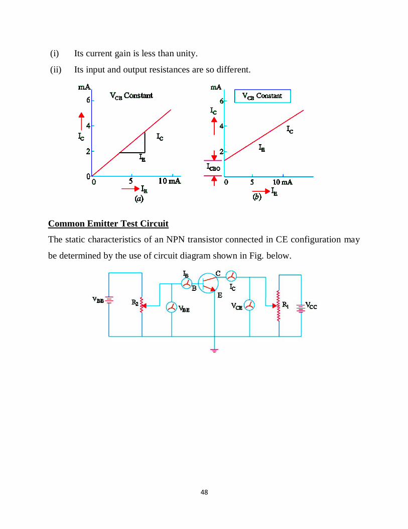
(i) Its current gain is less than unity.
(ii) Its input and output resistances are so different.
Common Emitter Test Circuit
The static characteristics of an NPN transistor connected in CE configuration may
be determined by the use of circuit diagram shown in Fig. below.
49
Common Emitter Static Characteristics
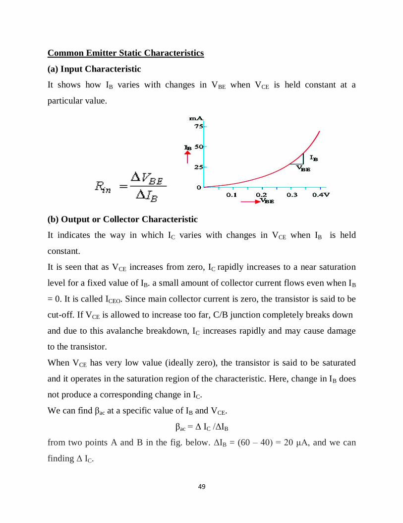
(a) Input Characteristic
It shows how IB varies with changes in VBE when VCE is held constant at a
particular value.
(b) Output or Collector Characteristic
It indicates the way in which IC varies with changes in VCE when IB is held
constant.
It is seen that as VCE increases from zero, IC rapidly increases to a near saturation
level for a fixed value of IB. a small amount of collector current flows even when IB
= 0. It is called ICEO. Since main collector current is zero, the transistor is said to be
cut-off. If VCE is allowed to increase too far, C/B junction completely breaks down
and due to this avalanche breakdown, IC increases rapidly and may cause damage
to the transistor.
When VCE has very low value (ideally zero), the transistor is said to be saturated
and it operates in the saturation region of the characteristic. Here, change in IB does
not produce a corresponding change in IC.
We can find βac at a specific value of IB and VCE.
βac = Δ IC /ΔIB
from two points A and B in the fig. below. ΔIB = (60 – 40) = 20 μA, and we can
finding Δ IC.
50
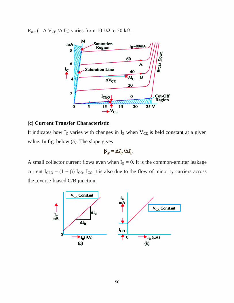
Rout (= Δ VCE /Δ IC) varies from 10 kΩ to 50 kΩ.
(c) Current Transfer Characteristic
It indicates how IC varies with changes in IB when VCE is held constant at a given
value. In fig. below (a). The slope gives
A small collector current flows even when IB = 0. It is the common-emitter leakage
current ICEO = (1 + β) ICO. ICO it is also due to the flow of minority carriers across
the reverse-biased C/B junction.
51
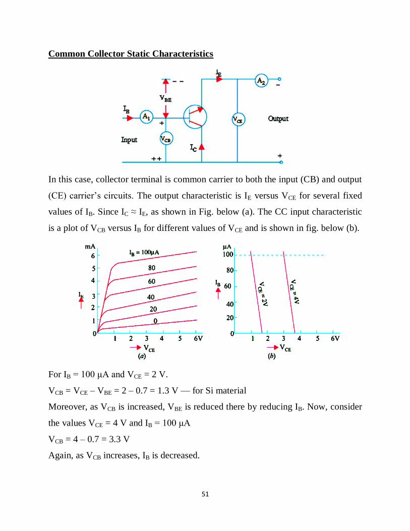
Common Collector Static Characteristics
In this case, collector terminal is common carrier to both the input (CB) and output
(CE) carrier’s circuits. The output characteristic is IE versus VCE for several fixed
values of IB. Since IC ≈ IE, as shown in Fig. below (a). The CC input characteristic
is a plot of VCB versus IB for different values of VCE and is shown in fig. below (b).
For IB = 100 μA and VCE = 2 V.
VCB = VCE – VBE = 2 – 0.7 = 1.3 V — for Si material
Moreover, as VCB is increased, VBE is reduced there by reducing IB. Now, consider
the values VCE = 4 V and IB = 100 μA
VCB = 4 – 0.7 = 3.3 V
Again, as VCB increases, IB is decreased.
52
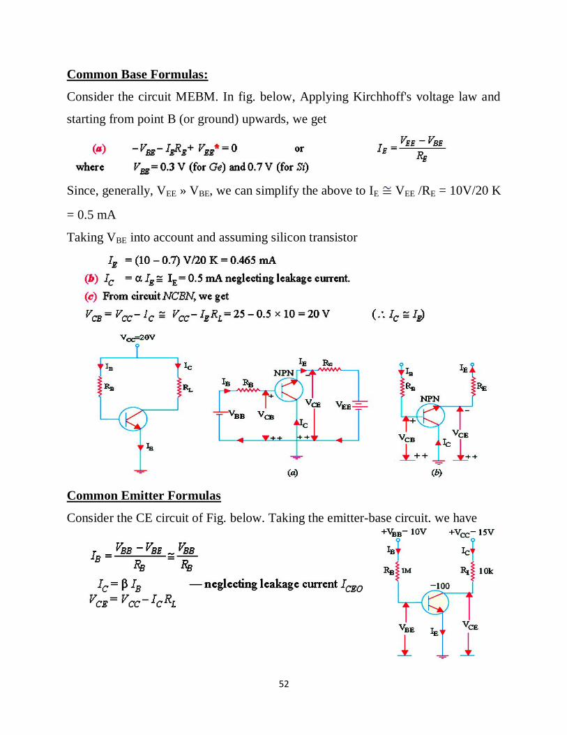
Common Base Formulas:
Consider the circuit MEBM. In fig. below, Applying Kirchhoff's voltage law and
starting from point B (or ground) upwards, we get
Since, generally, VEE » VBE, we can simplify the above to IE VEE /RE = 10V/20 K
= 0.5 mA
Taking VBE into account and assuming silicon transistor
Common Emitter Formulas
Consider the CE circuit of Fig. below. Taking the emitter-base circuit, we have
53
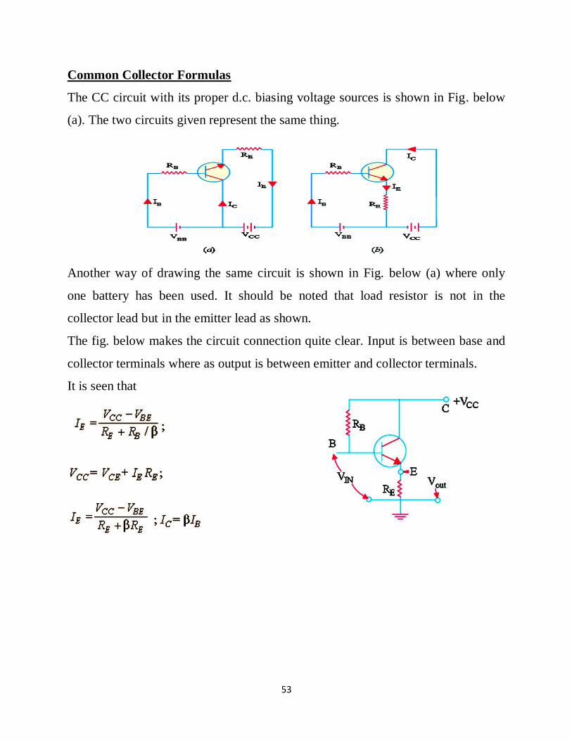
Common Collector Formulas
The CC circuit with its proper d.c. biasing voltage sources is shown in Fig. below
(a). The two circuits given represent the same thing.
Another way of drawing the same circuit is shown in Fig. below (a) where only
one battery has been used. It should be noted that load resistor is not in the
collector lead but in the emitter lead as shown.
The fig. below makes the circuit connection quite clear. Input is between base and
collector terminals where as output is between emitter and collector terminals.
It is seen that
54
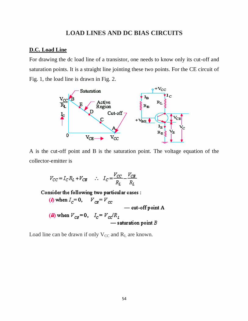
LOAD LINES AND DC BIAS CIRCUITS
D.C. Load Line
For drawing the dc load line of a transistor, one needs to know only its cut-off and
saturation points. It is a straight line jointing these two points. For the CE circuit of
Fig. 1, the load line is drawn in Fig. 2.
A is the cut-off point and B is the saturation point. The voltage equation of the
collector-emitter is
Load line can be drawn if only VCC and RL are known.
55
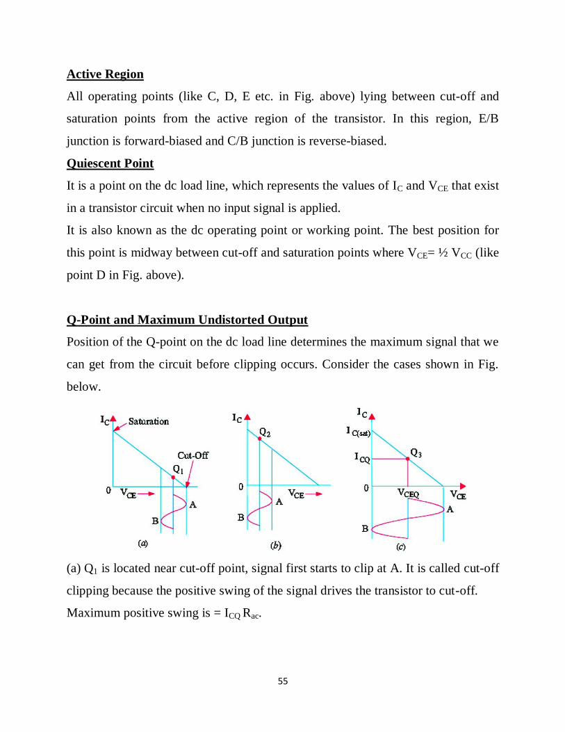
Active Region
All operating points (like C, D, E etc. in Fig. above) lying between cut-off and
saturation points from the active region of the transistor. In this region, E/B
junction is forward-biased and C/B junction is reverse-biased.
Quiescent Point
It is a point on the dc load line, which represents the values of IC and VCE that exist
in a transistor circuit when no input signal is applied.
It is also known as the dc operating point or working point. The best position for
this point is midway between cut-off and saturation points where VCE= ½ VCC (like
point D in Fig. above).
Q-Point and Maximum Undistorted Output
Position of the Q-point on the dc load line determines the maximum signal that we
can get from the circuit before clipping occurs. Consider the cases shown in Fig.
below.
(a) Q1 is located near cut-off point, signal first starts to clip at A. It is called cut-off
clipping because the positive swing of the signal drives the transistor to cut-off.
Maximum positive swing is = ICQ Rac.
56
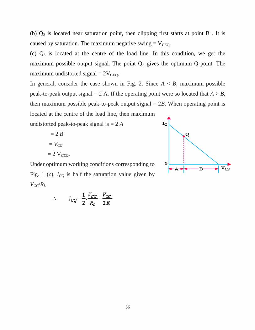
(b) Q2 is located near saturation point, then clipping first starts at point B . It is
caused by saturation. The maximum negative swing = VCEQ.
(c) Q3 is located at the centre of the load line. In this condition, we get the
maximum possible output signal. The point Q3 gives the optimum Q-point. The
maximum undistorted signal = 2VCEQ.
In general, consider the case shown in Fig. 2. Since A < B, maximum possible
peak-to-peak output signal = 2 A. If the operating point were so located that A > B,
then maximum possible peak-to-peak output signal = 2B. When operating point is
located at the centre of the load line, then maximum
undistorted peak-to-peak signal is = 2 A
= 2 B
= VCC
= 2 VCEQ.
Under optimum working conditions corresponding to
Fig. 1 (c), ICQ is half the saturation value given by
VCC/RL
57
Need For Biasing a Transistor
For normal operation of a transistor amplifier circuit, it is essential that there
should be a
(a) Forward bias on the emitter-base junction and
(b) Reverse bias on the collector-base junction.
In addition, amount of bias required is important for establishing the Q-point which
is dictated by the mode of operation desired. If the transistor is not biased
correctly, it would
1. Work inefficiently and
2. Produce distortion in the output signal.
Factors Affecting Bias Variations
In practice, it is found that even after careful selection, Q-point tends to shift its
position. This bias instability is the direct result of thermal instability which itself
is produced by cumulative increase in IC that may, if unchecked, lead to thermal
runaway. The collector current for CE circuit is given by
This equation has three variables: β, IB and ICO all of which are found to increase
with temperature. In particular, increase in ICO produces significant increase in
collector current IC. This leads to increased power dissipation with further increase
in temperature and hence IC. Being a cumulative process, it can lead to thermal
runaway which will destroy the transistor itself.
58
However, if by some circuit modification, IC is made to decrease with temperature
automatically, then decrease in the term βIB can be made to neutralize the increase
in the term (1 + β) ICO, thereby keeping IC constant. This will achieve thermal
stability resulting in bias stability.
Stability Factor
The degree of success achieved in stabilizing IC in the face of variations in ICO is
expressed in terms of current stability factor S. It is defined as the rate of change of
IC with respect to ICO when both β and IB (VBE) are held constant.
Larger the value of S, greater the thermal instability and vice versa. The stability
factor may be alternatively expressed by using the well-known equation
IC= I β+ (I + β) ICO
Which, on differentiation with respect to IC, yields.
59
Beta Sensitivity
Variations in β-value are caused by variations in the circuit operating conditions or
by the substitution of one transistor with another. Beta sensitivity Kβ is given by
Kβ is dimensionless ratio and can have values ranging from zero to unity.
Stability Factor for CB and CE Circuits
(i) CB Circuit
Here, collector current is given by
(ii) CE Circuit
If β = 100, then S = 101 which means that IC changes 101 times as much as ICO.
60
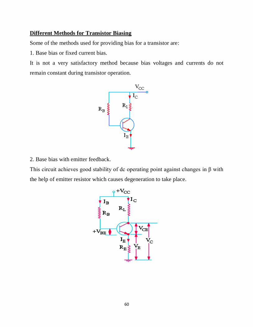
Different Methods for Transistor Biasing
Some of the methods used for providing bias for a transistor are:
1. Base bias or fixed current bias.
It is not a very satisfactory method because bias voltages and currents do not
remain constant during transistor operation.
2. Base bias with emitter feedback.
This circuit achieves good stability of dc operating point against changes in β with
the help of emitter resistor which causes degeneration to take place.
61
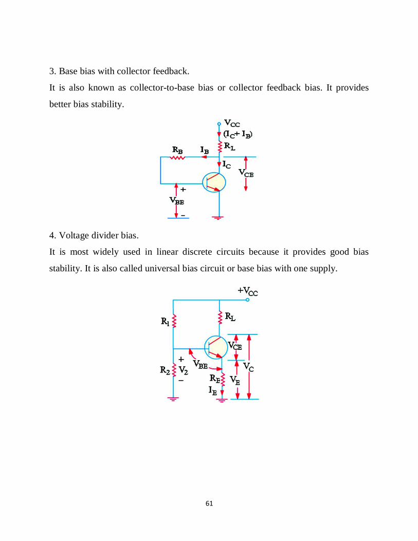
3. Base bias with collector feedback.
It is also known as collector-to-base bias or collector feedback bias. It provides
better bias stability.
4. Voltage divider bias.
It is most widely used in linear discrete circuits because it provides good bias
stability. It is also called universal bias circuit or base bias with one supply.
62
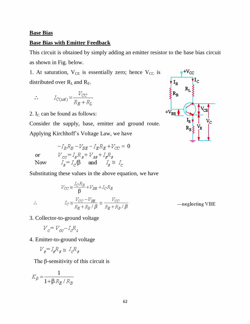
Base Bias
Base Bias with Emitter Feedback
This circuit is obtained by simply adding an emitter resistor to the base bias circuit
as shown in Fig. below.
1. At saturation, VCE is essentially zero; hence VCC is
distributed over RL and RE.
2. IC can be found as follows:
Consider the supply, base, emitter and ground route.
Applying Kirchhoff’s Voltage Law, we have
Substituting these values in the above equation, we have
3. Collector-to-ground voltage
4. Emitter-to-ground voltage
The β-sensitivity of this circuit is
63
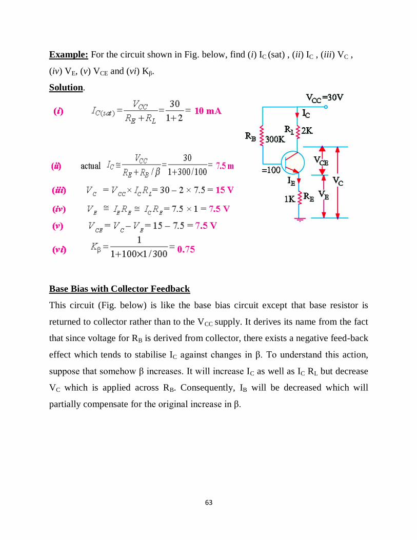
Example: For the circuit shown in Fig. below, find (i) IC (sat) , (ii) IC , (iii) VC ,
(iv) VE, (v) VCE and (vi) Kβ.
Solution.
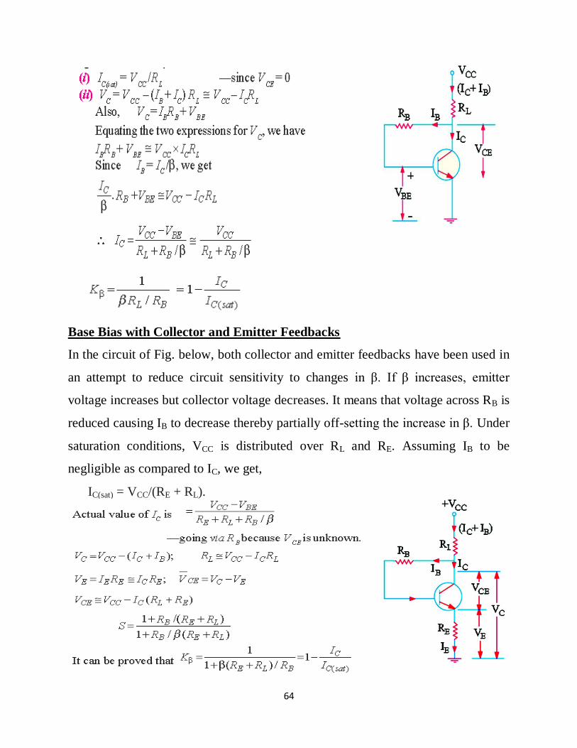
Base Bias with Collector Feedback
This circuit (Fig. below) is like the base bias circuit except that base resistor is
returned to collector rather than to the VCC supply. It derives its name from the fact
that since voltage for RB is derived from collector, there exists a negative feed-back
effect which tends to stabilise IC against changes in β. To understand this action,
suppose that somehow β increases. It will increase IC as well as IC RL but decrease
VC which is applied across RB. Consequently, IB will be decreased which will
partially compensate for the original increase in β.
64
Base Bias with Collector and Emitter Feedbacks
In the circuit of Fig. below, both collector and emitter feedbacks have been used in
an attempt to reduce circuit sensitivity to changes in β. If β increases, emitter
voltage increases but collector voltage decreases. It means that voltage across RB is
reduced causing IB to decrease thereby partially off-setting the increase in β. Under
saturation conditions, VCC is distributed over RL and RE. Assuming IB to be
negligible as compared to IC, we get,
IC(sat) = VCC/(RE + RL).
65
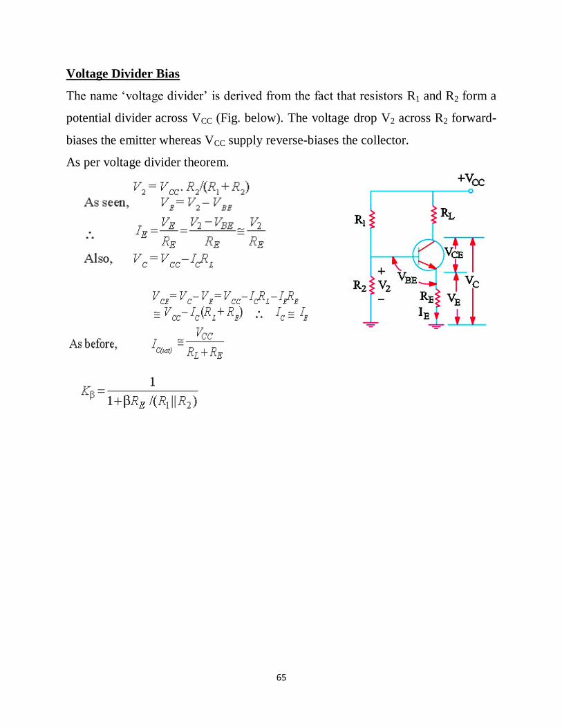
Voltage Divider Bias
The name ‘voltage divider’ is derived from the fact that resistors R1 and R2 form a
potential divider across VCC (Fig. below). The voltage drop V2 across R2 forward-
biases the emitter whereas VCC supply reverse-biases the collector.
As per voltage divider theorem.
66
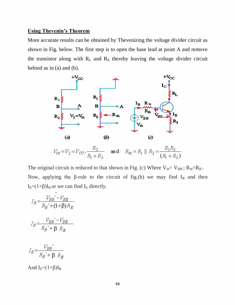
Using Thevenin’s Theorem
More accurate results can be obtained by Thevenizing the voltage divider circuit as
shown in Fig. below. The first step is to open the base lead at point A and remove
the transistor along with RL and RE thereby leaving the voltage divider circuit
behind as in (a) and (b).
The original circuit is reduced to that shown in Fig. (c) Where Vth= VBB´; Rth=RB´.
Now, applying the β-rule to the circuit of fig.(b) we may find IB and then
IE=(1+β)IB or we can find IE directly.
And IE=(1+β)IB
67
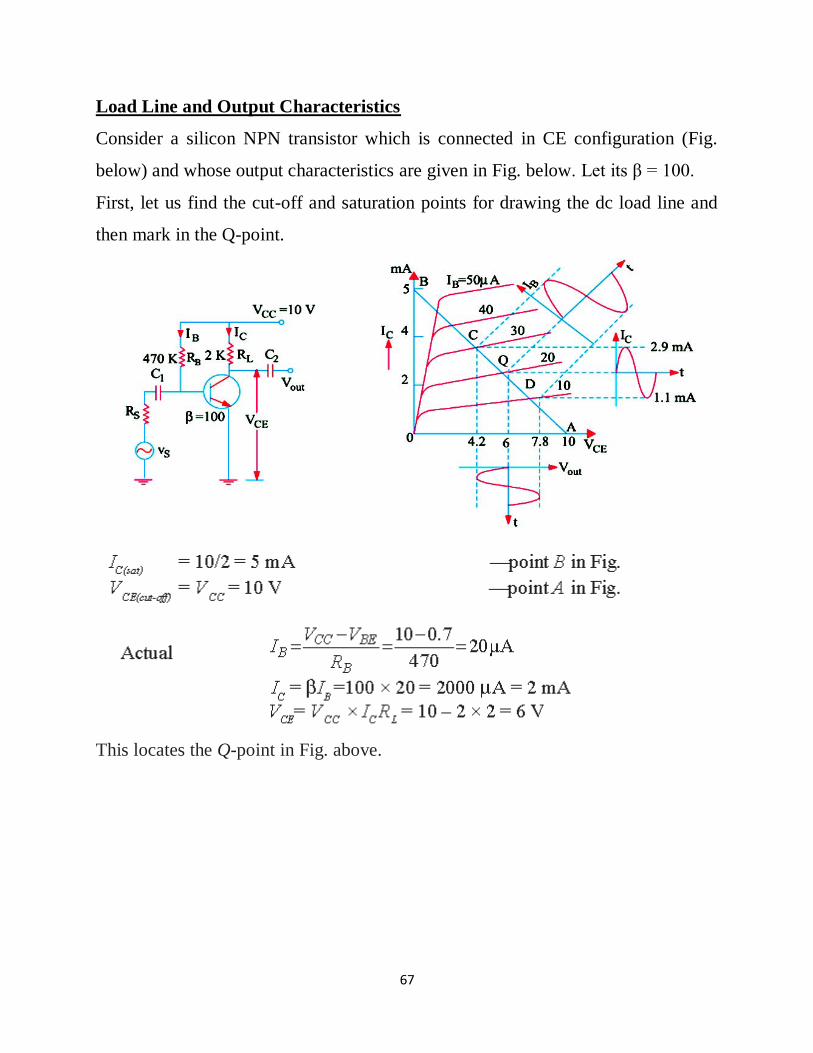
Load Line and Output Characteristics
Consider a silicon NPN transistor which is connected in CE configuration (Fig.
below) and whose output characteristics are given in Fig. below. Let its β = 100.
First, let us find the cut-off and saturation points for drawing the dc load line and
then mark in the Q-point.
This locates the Q-point in Fig. above.
68
Also
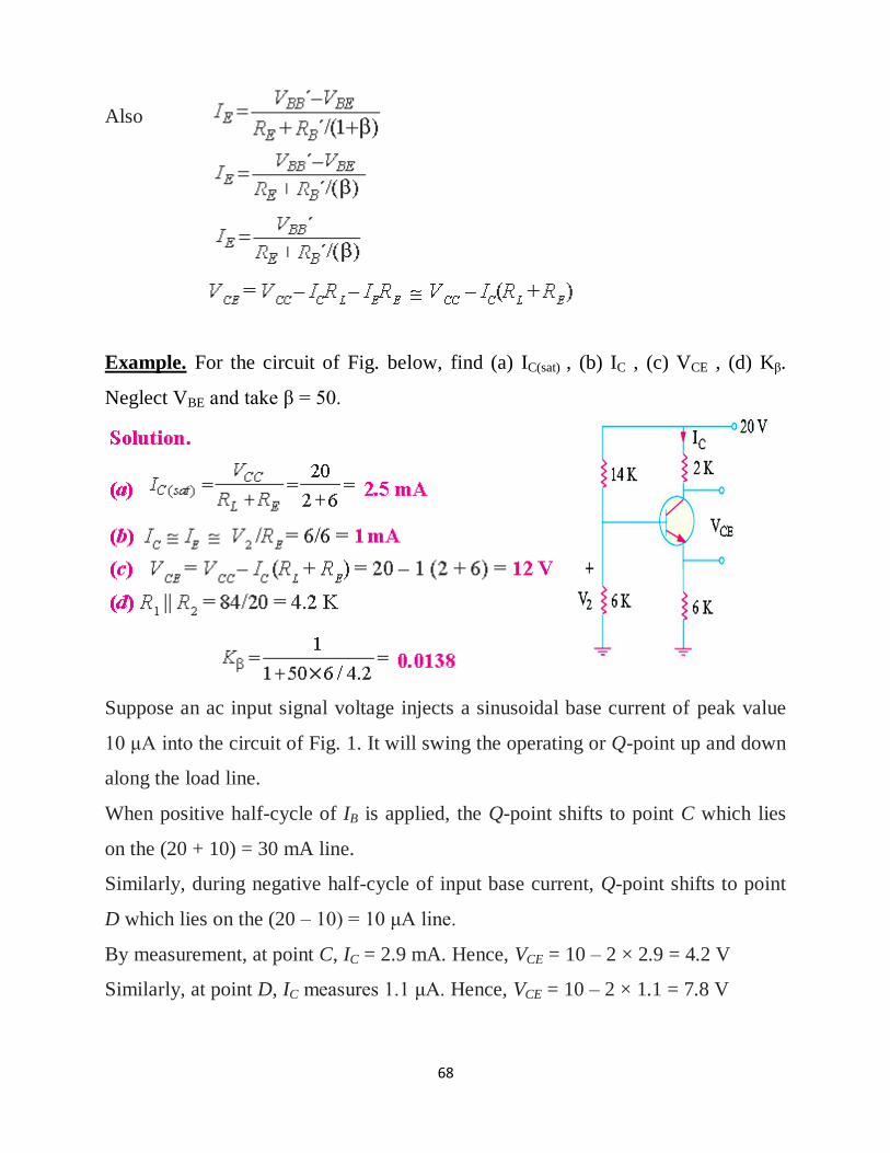
Example. For the circuit of Fig. below, find (a) IC(sat) , (b) IC , (c) VCE , (d) Kβ.
Neglect VBE and take β = 50.
Suppose an ac input signal voltage injects a sinusoidal base current of peak value
10 μA into the circuit of Fig. 1. It will swing the operating or Q-point up and down
along the load line.
When positive half-cycle of IB is applied, the Q-point shifts to point C which lies
on the (20 + 10) = 30 mA line.
Similarly, during negative half-cycle of input base current, Q-point shifts to point
D which lies on the (20 – 10) = 10 μA line.
By measurement, at point C, IC = 2.9 mA. Hence, VCE = 10 – 2 × 2.9 = 4.2 V
Similarly, at point D, IC measures 1.1 μA. Hence, VCE = 10 – 2 × 1.1 = 7.8 V
69
It is seen that VCE decreases from 6 V to 4.2 V by a peak value of (6-4.2) = 1.8 V
when base current goes positive. On the other hand, VCE increases from 6 V to 7.8
V by a peak value of (7.8 – 6) = 1.8 V when input base current signal goes
negative. Since changes in VCE represent changes in output voltage, it means that
when input signal is applied, IB varies according to the signal amplitude and causes
IC to vary. It may e noted that variation in voltage drop across RL are exactly the
same as in VCE.
Steady drop across RL when no signal is applied =2*2=4V. When signal goes
positive, drop across RL=2*2.9=5.8V.when base signal goes negative IC=1.1mA
and drop across RL= 2 × 1.1 = 2.2 V.
Hence, voltage variation is = 5.8 – 4 = 1.8 V during positive input half-cycle and
4 – 2.2 = 1.8 V during negative input half-cycle.
rms voltage variation = 1.8 2 = 1.27𝑉.
Now, proper dissipated in RL by ac component of output voltage is
𝑃𝑎𝑐 = 1.272 2 = 0.81 𝑚𝑊
𝑃𝑑𝑐 = 𝐼𝐶2𝑅𝐿 = 22 × 2 = 8𝑚𝑊
Total power dissipated in RL=8.81mW.
AC Load Line
It is the line along which Q-point shifts up and down when changes in output
voltage and current of an amplifier are caused by an ac signal.
This line is steeper than the dc line but the two intersect at the Q-point determined
by biasing dc voltage and currents.
AC load line takes into account the ac load resistance whereas dc load line
considers only the dc load resistance.
70
DC load line
The cut-off point for this line is where VCE=VCC. It is also written as VCE
(cut-off) saturation point is given by IC=VCC/RL. It is represented by straight line
AQB in Fig.1.
AC load line
The cut-off point is given by VCE(cut-off)=VCEQ+ICQRac ,where Rac is the ac
load resistance. Saturation point is given by
It is represented by straight line CQD in Fig.1. The slope of the ac load line is
given by y=-1/Rac.
It is seen from Fig. 1 that maximum possible positive signal swing is = ICQRac.
Similarly, maximum possible negative signal swing is VCEQ.
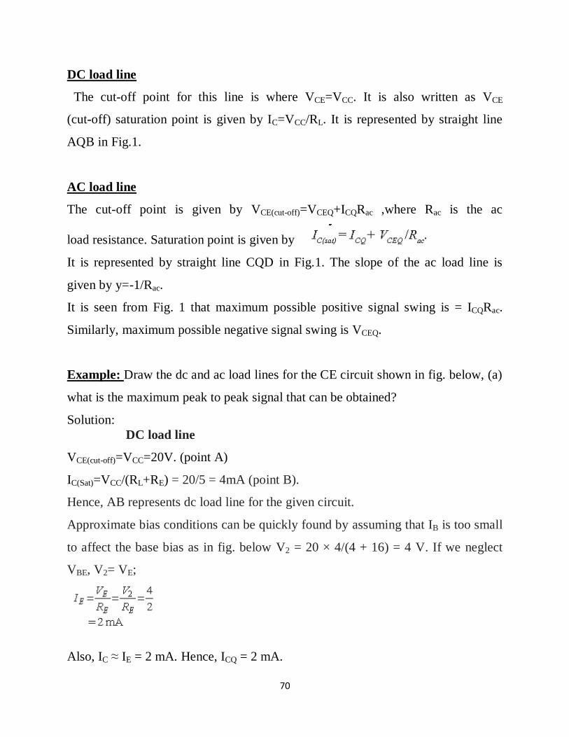
Example: Draw the dc and ac load lines for the CE circuit shown in fig. below, (a)
what is the maximum peak to peak signal that can be obtained?
Solution:
DC load line
VCE(cut-off)=VCC=20V. (point A)
IC(Sat)=VCC/(RL+RE) = 20/5 = 4mA (point B).
Hence, AB represents dc load line for the given circuit.
Approximate bias conditions can be quickly found by assuming that IB is too small
to affect the base bias as in fig. below V2 = 20 × 4/(4 + 16) = 4 V. If we neglect
VBE, V2= VE;
Also, IC ≈ IE = 2 mA. Hence, ICQ = 2 mA.
71
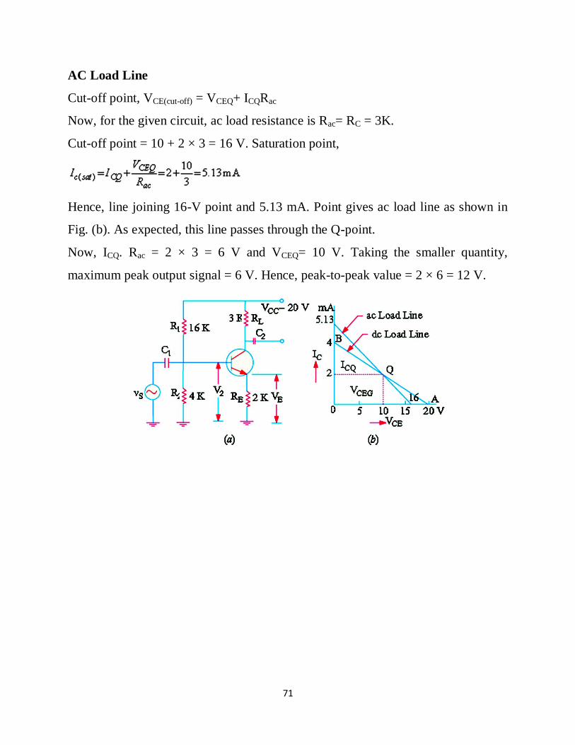
AC Load Line
Cut-off point, VCE(cut-off) = VCEQ+ ICQRac
Now, for the given circuit, ac load resistance is Rac= RC = 3K.
Cut-off point = 10 + 2 × 3 = 16 V. Saturation point,
Hence, line joining 16-V point and 5.13 mA. Point gives ac load line as shown in
Fig. (b). As expected, this line passes through the Q-point.
Now, ICQ. Rac = 2 × 3 = 6 V and VCEQ= 10 V. Taking the smaller quantity,
maximum peak output signal = 6 V. Hence, peak-to-peak value = 2 × 6 = 12 V.
72
What are h-parameter?
These are four constants which describe the behavior of a two-port linear
network. A linear network is one in which resistance, inductances and capacitances
remain fixed when voltage across them is changed.
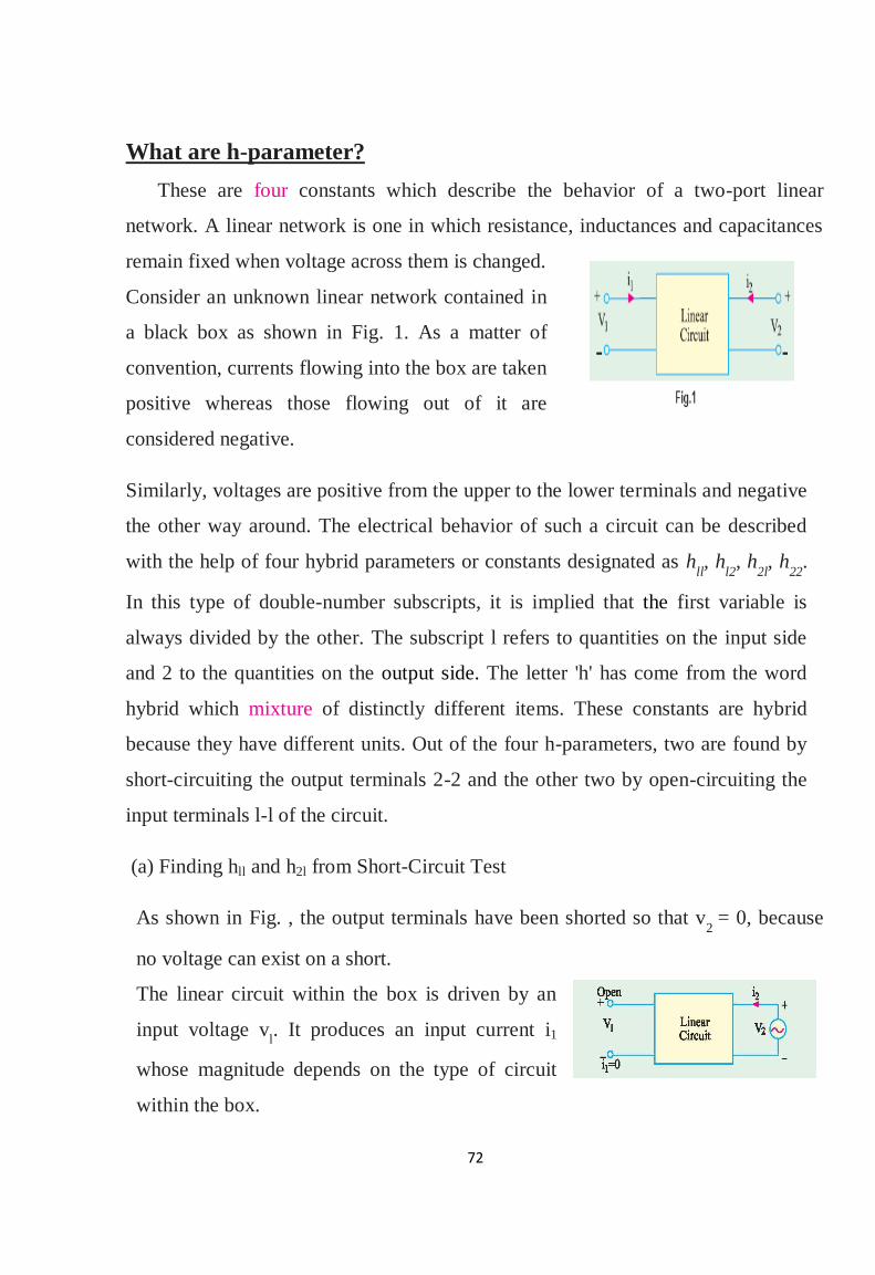
Consider an unknown linear network contained in
a black box as shown in Fig. 1. As a matter of
convention, currents flowing into the box are taken
positive whereas those flowing out of it are
considered negative.
Similarly, voltages are positive from the upper to the lower terminals and negative
the other way around. The electrical behavior of such a circuit can be described
with the help of four hybrid parameters or constants designated as hll, h
l2, h
2l, h
22.
In this type of double-number subscripts, it is implied that the first variable is
always divided by the other. The subscript l refers to quantities on the input side
and 2 to the quantities on the output side. The letter 'h' has come from the word
hybrid which mixture of distinctly different items. These constants are hybrid
because they have different units. Out of the four h-parameters, two are found by
short-circuiting the output terminals 2-2 and the other two by open-circuiting the
input terminals l-l of the circuit.
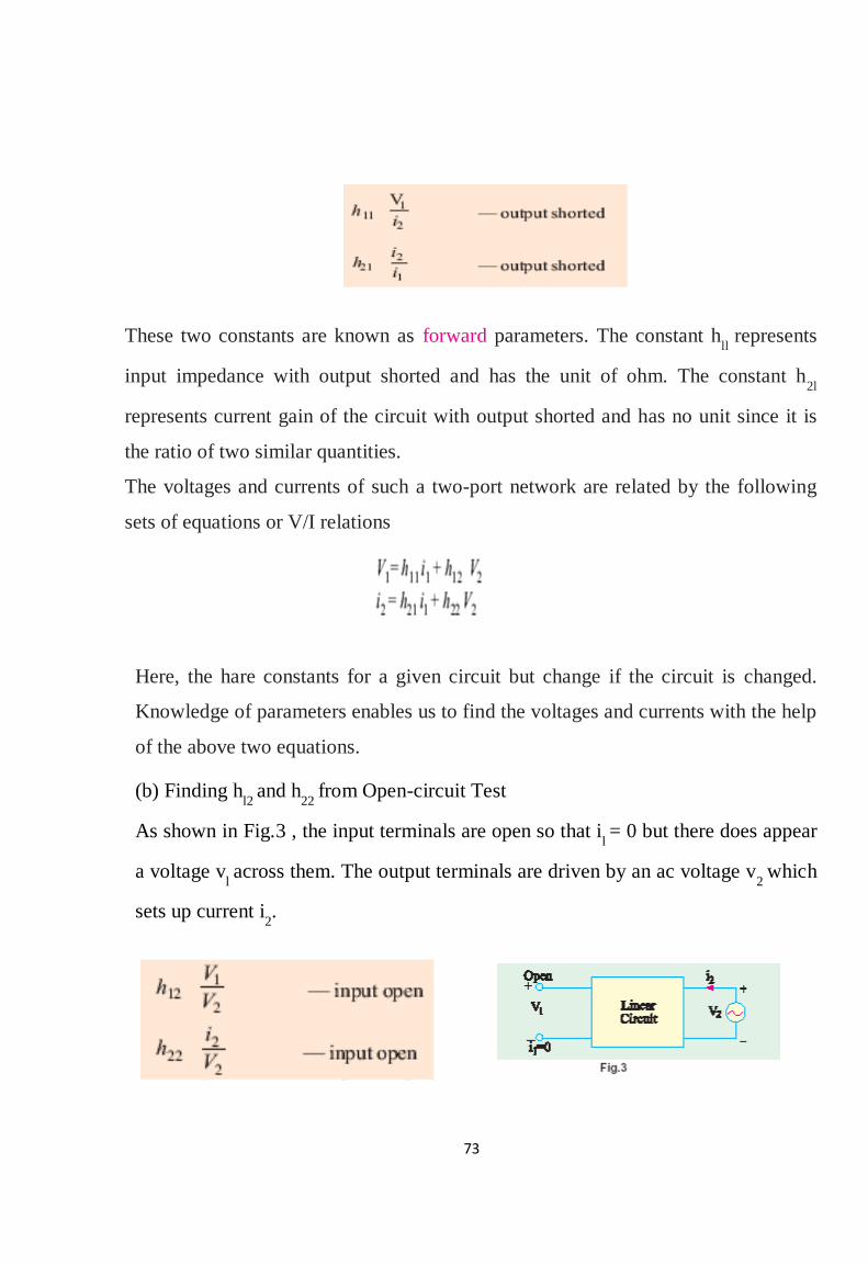
(a) Finding hll and h2l from Short-Circuit Test
As shown in Fig. , the output terminals have been shorted so that v2
= 0, because
no voltage can exist on a short.
The linear circuit within the box is driven by an
input voltage vl. It produces an input current i1
whose magnitude depends on the type of circuit
within the box.
73
These two constants are known as forward parameters. The constant hll
represents
input impedance with output shorted and has the unit of ohm. The constant h2l
represents current gain of the circuit with output shorted and has no unit since it is
the ratio of two similar quantities.
The voltages and currents of such a two-port network are related by the following
sets of equations or V/I relations
Here, the hare constants for a given circuit but change if the circuit is changed.
Knowledge of parameters enables us to find the voltages and currents with the help
of the above two equations.
(b) Finding hl2
and h22
from Open-circuit Test
As shown in Fig.3 , the input terminals are open so that il = 0 but there does appear
a voltage vl across them. The output terminals are driven by an ac voltage v
2 which
sets up current i2.
74
As seen, hl2
represents voltage gain (not forward gain which is v2
/ v l). Hence, it
has no units. The constant h22
represents admittance (which is reverse of
resistance) and has the unit of mho or Siemens, s.
It is actually the admittance looking into the output terminals with input terminals
open. Generally, these two constants are also referred to as reverse parameters.
The h-parameter Notation for Transistors
While using h-parameters for transistor circuits, their numerical subscripts are
replaced by the first letters for defining them.
A second subscript is added to the above parameters to indicate the particular
configuration. For example, for CE connection, the four parameters are written as
hie, hfe, hre, hoe. Similarly, for CB connection, these are written as hib
, hfb
, hrb
and for
CC connection as hic, hfc, hrc and hoc
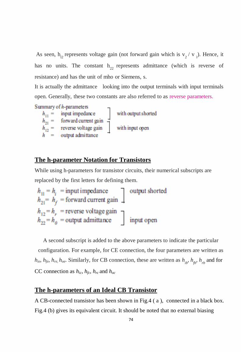
The h-parameters of an Ideal CB Transistor
A CB-connected transistor has been shown in Fig.4 ( a ), connected in a black box.
Fig.4 (b) gives its equivalent circuit. It should be noted that no external biasing
75
resistors or any signal source has been shown connected to the transistor.
(i) Forward Parameters
The two forward h-parameters can be found from the circuit of Fig.4 ( a) where a
short has been put across the output. The input impedance is simply re.
The output current equals the input current i.e. Since it flows out of the box, it is
taken as negative. The forward current gain is
(It also called the ac α of the CB circuit.)
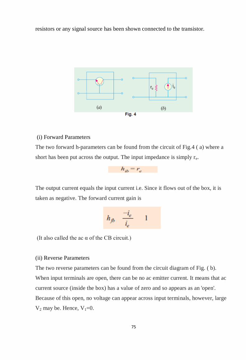
(ii) Reverse Parameters
The two reverse parameters can be found from the circuit diagram of Fig. ( b).
When input terminals are open, there can be no ac emitter current. It means that ac
current source (inside the box) has a value of zero and so appears as an 'open'.
Because of this open, no voltage can appear across input terminals, however, large
V2 may be. Hence, V1=0.
76
Similarly, the impedance, looking into the output terminals is infinite.
Consequently, its admittance (= l/∞) is zero.
The four h-parameters of an ideal transistor connected in CB configuration are;
The equivalent hybrid circuit is shown in Fig. 5.
In reality, output impedance is not infinity but very high so that hob
is extremely
small. Similarly, there is some amount of feedback between the output and the input
77
circuits (even when open) though it is very small. Hence, h is very small.
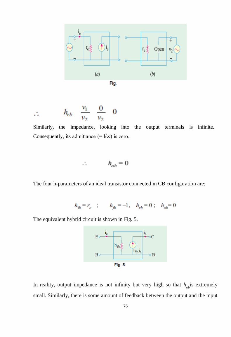
The h--parameters of an ideal CE Transistor
Fig 6 (a) shows a CE-connected ideal transistor contained in a black box where
shows its ac equivalent circuit in terms of its β and resistance values.
(a) Forward Parameters
The two forward h-parameters can be found from the circuit of Fig.7 (a)
Where output has been shorted. Obviously, the input impedance is simply βre
The forward current gain is given by
(It is also called the ac beta of the CE circuit)
(b) Reverse Parameters
These can be found by reference to the circuit of Fig.7 (b), where input terminals
are open but output terminals are driven by an are voltage source v2 With input
terminals open, there can be no base current so that ib = o. If ib= o, then collector
current source has zero value ib and looks like an open. Hence, there can be no v1
due to this open.
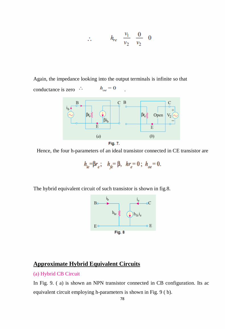
78
Again, the impedance looking into the output terminals is infinite so that
conductance is zero .
Hence, the four h-parameters of an ideal transistor connected in CE transistor are
The hybrid equivalent circuit of such transistor is shown in fig.8.
Approximate Hybrid Equivalent Circuits
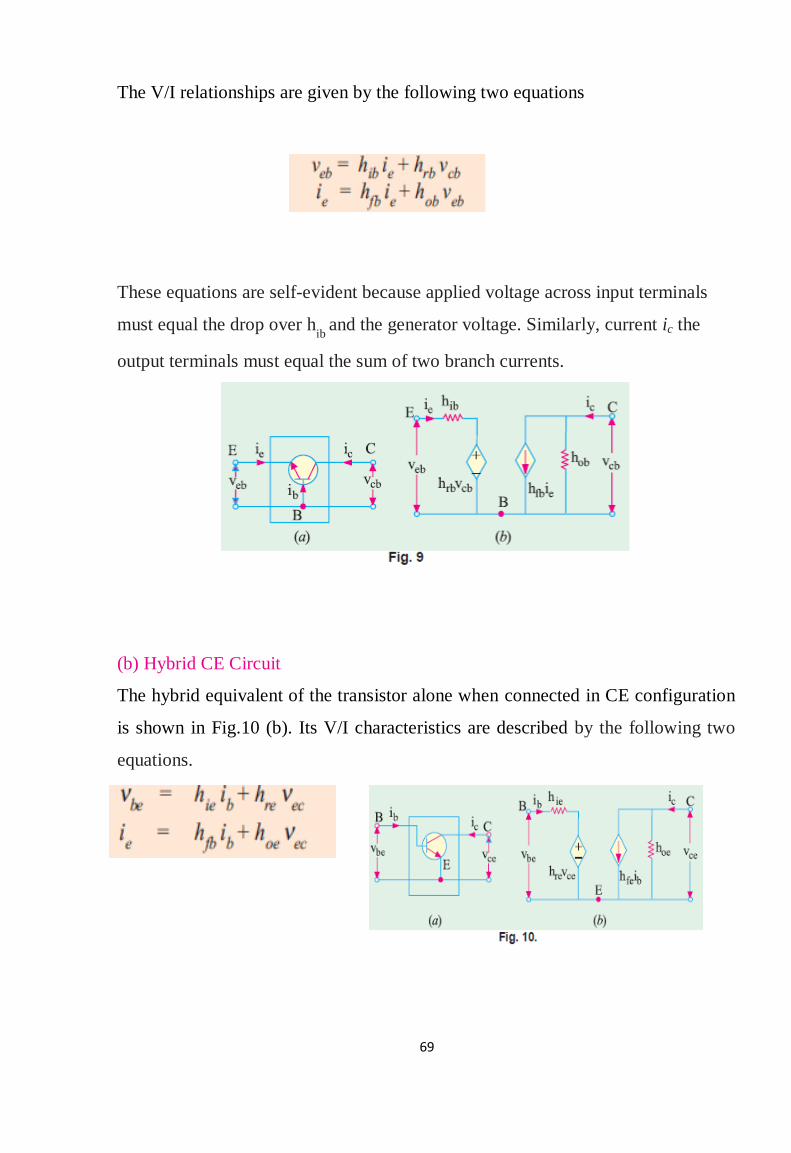
(a) Hybrid CB Circuit
In Fig. 9. ( a) is shown an NPN transistor connected in CB configuration. Its ac
equivalent circuit employing h-parameters is shown in Fig. 9 ( b).
69
The V/I relationships are given by the following two equations
These equations are self-evident because applied voltage across input terminals
must equal the drop over hib
and the generator voltage. Similarly, current ic the
output terminals must equal the sum of two branch currents.
(b) Hybrid CE Circuit
The hybrid equivalent of the transistor alone when connected in CE configuration
is shown in Fig.10 (b). Its V/I characteristics are described by the following two
equations.
70
Parameter CB CE
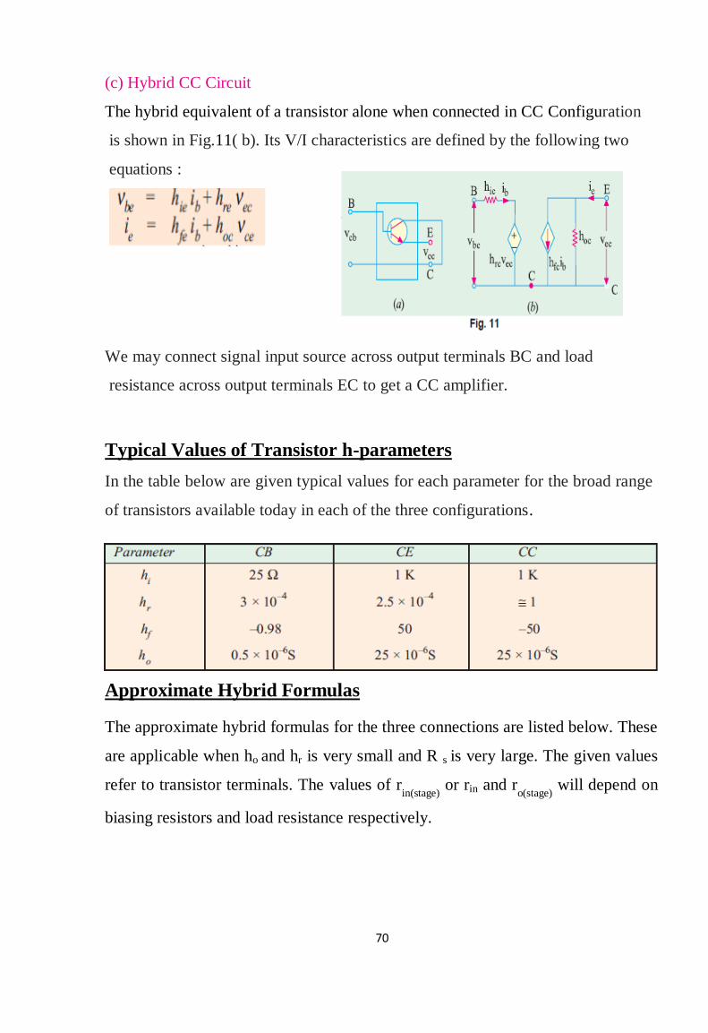
(c) Hybrid CC Circuit
The hybrid equivalent of a transistor alone when connected in CC Configuration
is shown in Fig.11( b). Its V/I characteristics are defined by the following two
equations :
We may connect signal input source across output terminals BC and load
resistance across output terminals EC to get a CC amplifier.
Typical Values of Transistor h-parameters
In the table below are given typical values for each parameter for the broad range
of transistors available today in each of the three configurations.
Approximate Hybrid Formulas
The approximate hybrid formulas for the three connections are listed below. These
are applicable when ho and hr is very small and R s is very large. The given values
refer to transistor terminals. The values of rin(stage)
or rin and ro(stage)
will depend on
biasing resistors and load resistance respectively.
71
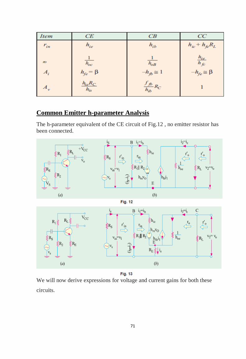
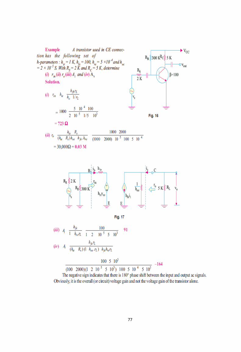
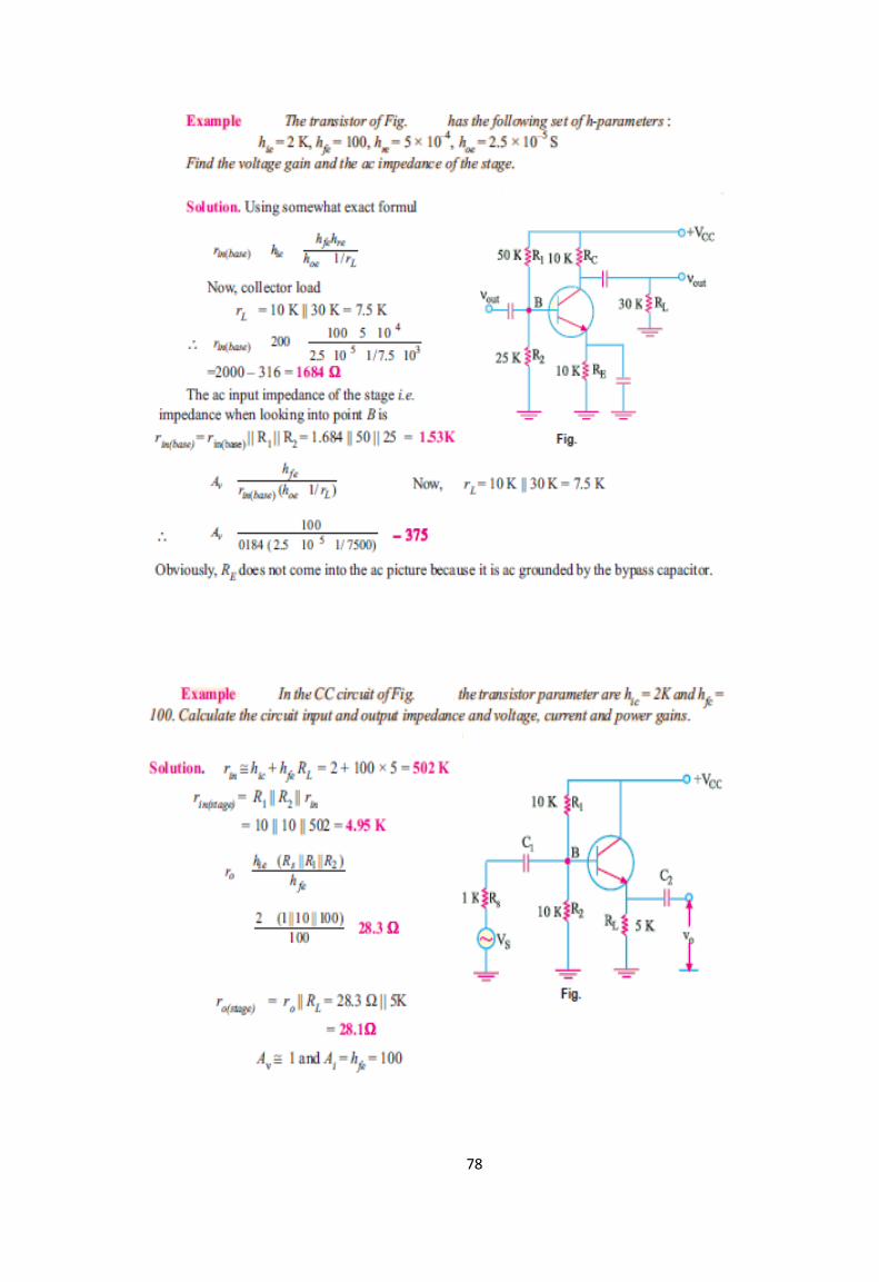
Common Emitter h-parameter Analysis
The h-parameter equivalent of the CE circuit of Fig.12 , no emitter resistor has
been connected.
We will now derive expressions for voltage and current gains for both these
circuits.
72
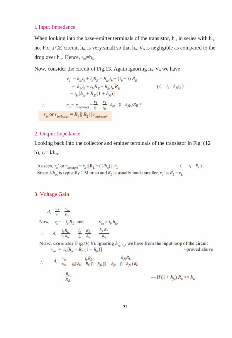
l. Input Impedance
When looking into the base-emitter terminals of the transistor, hie in series with hre
no. For a CE circuit, hre is very small so that hre Vo is negligible as compared to the
drop over hie. Hence, rin=hie.
Now, consider the circuit of Fig.13. Again ignoring hre Vo we have
2. Output Impedance
Looking back into the collector and emitter terminals of the transistor in Fig. (12
b), ro= l/hoe .
3. Voltage Gain
73
4. Current Gain
5. Power Gain
Common Collector h-parameter Analysis
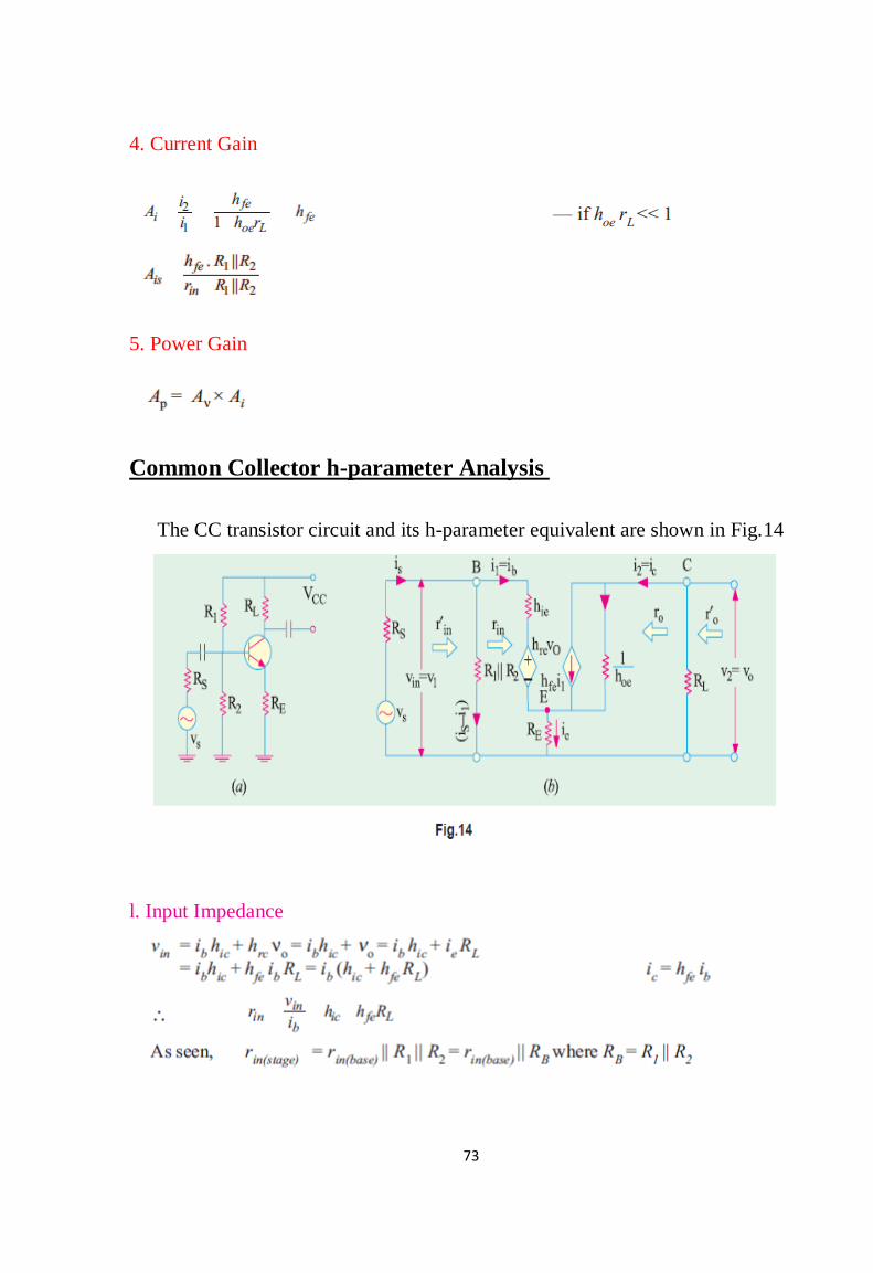
The CC transistor circuit and its h-parameter equivalent are shown in Fig.14
l. Input Impedance
74
2. Output Impedance
75
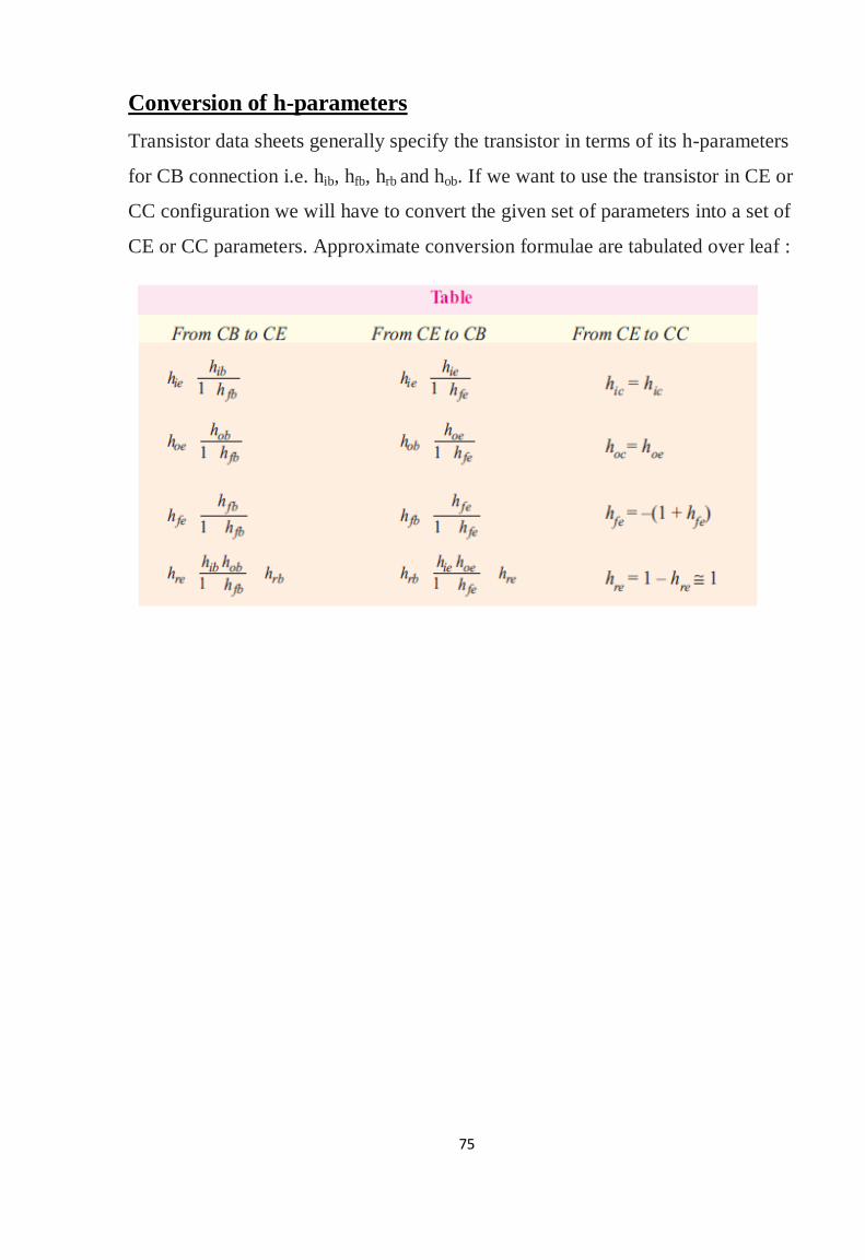
Conversion of h-parameters
Transistor data sheets generally specify the transistor in terms of its h-parameters
for CB connection i.e. hib, hfb, hrb and hob. If we want to use the transistor in CE or
CC configuration we will have to convert the given set of parameters into a set of
CE or CC parameters. Approximate conversion formulae are tabulated over leaf :
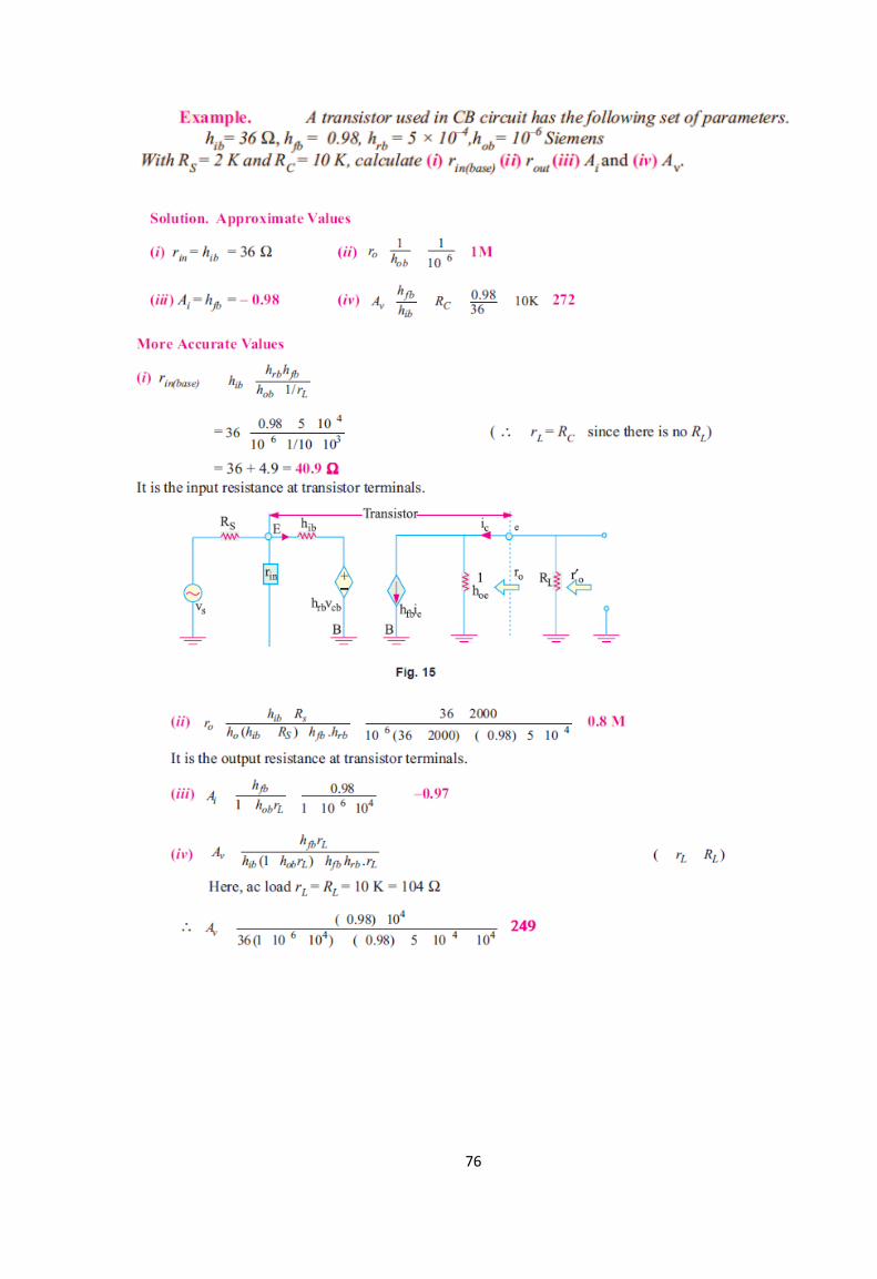
76
77
78
79
1.What is an OP-AMP ?
It is a very high-gain, amplifier which can amplify signals having frequency
ranging from 0 Hz to a little beyond 1 MHz. They are made with different
internal configurations in linear ICs. An OP-AMP is so named because it was
originally designed to perform mathematical operations like summation,
subtraction, multiplication, differentiation and integration etc. in analog computers.
Present day usage is much wider in scope but the popular name OP-AMP
continues.
Although an OP-AMP is a complete amplifier, it is so designed that external
components (resistors, capacitors etc.) can be connected to its terminals to change
its external characteristics. Hence, it is relatively easy to tailor this amplifier to fit a
particular application and it is, in fact, due to this versatility that OP-AMPs have
become so popular in industry.
2. OP-AMP Symbol
Standard triangular symbol for an OP-AMP is shown in Fig.1 (a) though the one
shown in Fig.1 (b) is also used often. In Fig.1 (b), the common ground line has
been omitted. It also does not show other necessary connections such as for dc
power and feedback etc. The OP-AMP’s input can be single ended or double-ended
(or differential input) depending on whether input voltage is applied to one input
terminal only or to both. Similarly, amplifier’s output can also be either single-
ended or double ended.
The most common configuration is two input terminals and a single output.
All OP-AMPs have a minimum of five terminals :
1. inverting input terminal, 2. non-inverting input terminal,
3. output terminal, 4. positive bias supply terminal,