Embed Size (px)
Citation preview

TRANSISTOR AMPLIFIERSAET 8
First Transistor developed at Bell Labs on December 16, 1947

TRANSISTOR AMPLIFIERS
Objective 1a
Identify Bipolar Transistor Amplifier Operating Principles

TRANSISTOR AMPLIFIERS
(1) Dynamic Operation(2) Configurations(3) Common Emitter(4) Common Collector(5) Common Base(6) Temperature Stabilization(7) Coupling
Overview
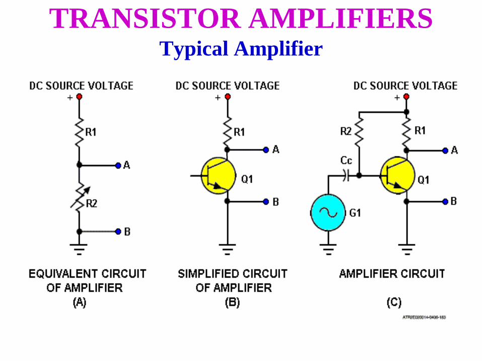
TRANSISTOR AMPLIFIERSTypical Amplifier

TRANSISTOR AMPLIFIERSTypical Amplifier
(A). Output taken from A to B:
Reduce the resistance of R2, voltage from A to B decreases.
Increase the resistance of R2, voltage from A to B increases.
(Voltage follows resistance)!

TRANSISTOR AMPLIFIERSTypical Amplifier
Resistor (R2) is replaced with transistor (Q1)
(B). Output taken from A to B:Reduce the resistance of Q1,
voltage from A to B decreases.
Increase the resistance of Q1, voltage from A to B increases.
(Voltage follows resistance)!

TRANSISTOR AMPLIFIERSTypical Amplifier
(C)An input signal from G1 is applied to the base through CC. The input signal changes the Bias on the base of the transistor controlling the current flow through the transistor.
The output, taken from A to B, will be a reproduction of the input signal only much larger.
TRANSISTOR AMPLIFIERS
Amplification: The ability of a circuit to receive a small change of input voltage or current (signal) and produce a largechange in the output voltage or current (signal).Amplification depends on the change in the transistor’s resistance caused by an input signal.

TRANSISTOR AMPLIFIERSCONFIGURATIONS

TRANSISTOR AMPLIFIERSCommon Emitter
Common Emitter is sometimes called the Grounded Emitter.
Input signal is applied to the base.
Output signal is taken from the collector.
The common line, (not used for signal) is connected to the emitter.

TRANSISTOR AMPLIFIERSCommon Collector
Common Collector (CC) is sometimes called Grounded Collector.The input signal is applied to the base.
The output signal is taken from the emitter.
The common line, (not used for signal) is connected to the collector.

TRANSISTOR AMPLIFIERSCommon Base
Common Base (CB) is sometimes called Grounded Base.
The input signal is applied to the emitter.
The output signal is taken from the collector.
The common line, (not used for signal) is connected to the base.

TRANSISTOR AMPLIFIERSCommon Emitter Amplifier
The purpose of the common emitter amplifier is to provide good current, voltage, and power gain.
180° phase shift

TRANSISTOR AMPLIFIERSCommon Emitter Amplifier Components
R1 determines forward bias
R2 aids in developing bias
R3 is the collector load resistor used to develop the output signal
R4 is the emitter resistor used for thermal stability

TRANSISTOR AMPLIFIERSCommon Emitter Amplifier Components
Q1 - transistor
C1 is the input coupling capacitor

TRANSISTOR AMPLIFIERSCommon Emitter Amplifier
Current paths and percentage of flow
IE = 100%, IC = 95%, IB = 5%
NPN – Current flows from Ground to +VCC

TRANSISTOR AMPLIFIERSCommon Emitter Amplifier
Signal path: When a signal is applied to an amplifier, four things occur.
Base, emitter & collector currents change at the rate of the input signal
Collector voltage changes at the rate of the input signal
Phase shift of 180°
There will be signal gain!

TRANSISTOR AMPLIFIERSCommon Emitter Amplifier
Static or Quiescent Operation
By definition, bias is defined as the average DC voltage (or current) used to establish the operating point in transistor circuits for a static or quiescent condition. A static condition means the circuit does not have an input signal and is fixed in a non-varying condition.

TRANSISTOR AMPLIFIERSTypical Amplifier with Bias - Static Condition
Transistor Current Path
600mv (.6v) Bias (emitter to base voltage) causes emitter current (IE), base current (IB), and collector current (IC) to flow.

TRANSISTOR AMPLIFIERSTypical Amplifier with Bias - Static Condition
Current enters the emitter and exits the base.
Current enters the emitter and exits the collector through R1 to VCC.
TRANSISTOR AMPLIFIERSCommon Emitter Amplifier
Dynamic Operation
The varying condition of a circuit is called its dynamic condition or operating condition. This occurs whenever an input signal is applied.

TRANSISTOR AMPLIFIERSTypical Amplifier with Bias - Dynamic
Dynamic condition: DC Bias with signal added (Varying condition) The output voltage has a much larger voltage change than the input.

TRANSISTOR AMPLIFIERSTypical Amplifier with Bias - Dynamic
Notice the .2V Pk-Pk signal at the input is using the .6v DC as its reference and the output 10V Pk-Pk signal is using the 15V DC as its reference.

TRANSISTOR AMPLIFIERSCommon Emitter Amplifier

TRANSISTOR AMPLIFIERSNPN Common Emitter Amplifier Operation
The negative alternation of the input signal applied to the base of the transistor causes forward bias to decrease and collector current to decrease.
The voltage drop across R3 decreases because IC decreased
The collector voltage (VC) increases
The bias decrease caused an increase in output voltage and produced a 180 phase inversion

TRANSISTOR AMPLIFIERSNPN Common Emitter Amplifier Operation
The positive alternation of the input signal applied to the base causes forward bias to increase and collector current to increase
The voltage drop across R3 increases because IC increased
The collector voltage (VC) decreases
The bias increase caused a decrease in output voltage and produced a 180 phase inversion

TRANSISTOR AMPLIFIERSCommon Emitter Amplifier

TRANSISTOR AMPLIFIERSCommon Emitter Amplifier
NPN with conventional power connectionVCC to base and
collector using respective resistors (R1 & R2).
TRANSISTOR AMPLIFIERSCommon Emitter Amplifier
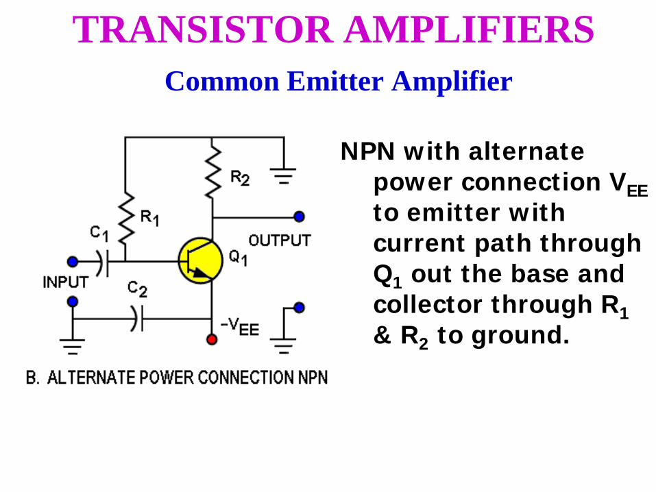
NPN with alternate power connection VEEto emitter with current path through Q1 out the base and collector through R1& R2 to ground.

TRANSISTOR AMPLIFIERSCommon Emitter Amplifier
PNP with conventional power connection-VCC to base and collector using respective resistors (R1 & R2).

TRANSISTOR AMPLIFIERSCommon Emitter Amplifier
PNP with alternate power connection +VEE to emitter with current path in the base and collector through R1 & R2 out the emitter to ground.

TRANSISTOR AMPLIFIERSCommon Emitter Amplifier
Characteristic Curve Graph
A transistor CHARACTERISTIC CURVE is a graph plotting of the relationships between currents and voltages in a transistor circuit.
The graph is then called a FAMILY of curves.

TRANSISTOR AMPLIFIERSCommon Emitter Amplifier
Characteristic Curve Graph
Graph shows base current (IB) changes vs. collector current (IC).
Graph shows a change in VCC vs. IC

Point B -Saturation
Point A -Cutoff
Base current - IB

TRANSISTOR AMPLIFIERSCommon Emitter Amplifier
Amplifier Gain – A ratio of the change in output to the change in input expressed as a formula:

TRANSISTOR AMPLIFIERSCommon Emitter Amplifier
Bias vs. Gain Characteristics
Optimum has the best gain
R2 is directly proportional to bias, resistance increases forward bias increases
R1 is inversely proportional to bias

TRANSISTOR AMPLIFIERSCommon Emitter Amplifier
Collector Load Resistor Changes
Increasing the resistance of R3 will cause a corresponding increase in the amount of change in collector voltage and increase in voltage gain.
Gain is directly proportional to the resistance value of R3.

Increasing R2 to 6KΩchanges the load line and gain increases from 10V to 12.5 volts.
Point B-Saturation

TRANSISTOR AMPLIFIERSClass of Operation
There are four classes of operation for amplifiers: A, AB, B and C
The class of operation is determined by the amount of forward bias.

TRANSISTOR AMPLIFIERSCommon Emitter Amplifier – Class A
Class A amplifiers have an exact reproduction of the input in the output. Conducts 100% of the timeThe collector current will flow for 360 degrees of the input signal

Class ‘A’ Amplifier Curve
IC
VCE
IB
0 uA
10 uA
20 uA
30 uA
40 uA
50 uA
60 uA
70 uA80 uA90 uA
Saturation
Cutoff
Q-Point

TRANSISTOR AMPLIFIERSCommon Emitter Amplifier – Class AB
Class AB amplifiers has some amplitude distortion and conducts 51% to 99% of the time.

Class ‘AB’ Amplifier Curve
IC
VCE
IB
0 uA
10 uA
20 uA
30 uA
40 uA
50 uA
60 uA
70 uA
80 uA
90 uA
Saturation
Cutoff
Q-Point

TRANSISTOR AMPLIFIERSCommon Emitter Amplifier – Class B
Class B amplifiers has amplitude and crossover distortion. Conducts 50% of the time.
The collector current will flow for 180 degrees of the input signal.

Class ‘B’ Amplifier Curve
IC
VCE
IB
0 uA
10 uA
20 uA
30 uA
40 uA
50 uA
60 uA
70 uA
80 uA
90 uA
Saturation
Cutoff
Q-Point
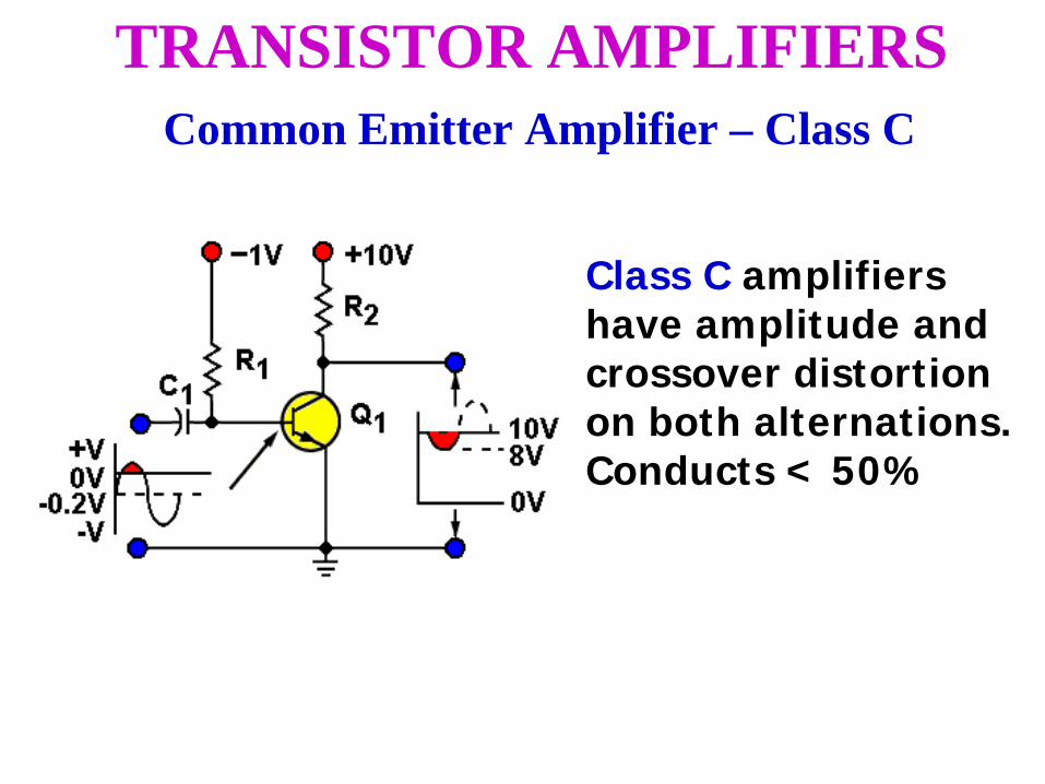
TRANSISTOR AMPLIFIERSCommon Emitter Amplifier – Class C
Class C amplifiers have amplitude and crossover distortion on both alternations. Conducts < 50%

Class ‘C’ Amplifier Curve
IC
VCE
IB
0 uA
10 uA
20 uA
30 uA
40 uA
50 uA
60 uA
70 uA
80 uA
90 uA
Saturation
CutoffQ-Point
TRANSISTOR AMPLIFIERS
Fidelity – The degree to which a device accurately reproduces at its output the characteristics of its input signal.
Class A has the best fidelity
Efficiency – The ratio between the output signal power and the total input power.
Class C has the best efficiency.

TRANSISTOR AMPLIFIERS
Amplitude Distortion – The result of changing a waveshape so its amplitude is no longer proportional to the original amplitude.
Amplitude distortion caused by too large input signal, excessive bias, or insufficient forward bias.

TRANSISTOR AMPLIFIERSClass of Operation Chart
TRANSISTOR AMPLIFIERSCommon Base Amplifier
The common base amplifier is also known as the grounded base amplifier.
The common base amplifier has a voltage gain greater than one, but it has a current gain less than one.
It is normally characterized by a very small input impedance and a high output impedance like the common emitter amplifier.
The input signal is in phase with the output signal.

TRANSISTOR AMPLIFIERSCommon Base Amplifier
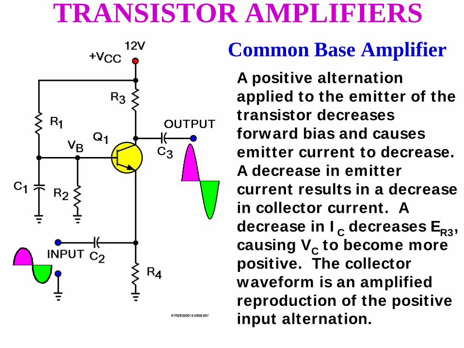
R1 provides forward bias for the emitter-base junction
R2 aids in developing forward bias
R3 is the collector load resistor
R4 develops the input signal

TRANSISTOR AMPLIFIERSCommon Base Amplifier
C1 places the base at AC ground
C2 is the input coupling capacitor
C3 is the Output coupling capacitor
Q1 NPN transistor
TRANSISTOR AMPLIFIERSCommon Base Amplifier
A positive alternation applied to the emitter of the transistor decreases forward bias and causes emitter current to decrease. A decrease in emitter current results in a decrease in collector current. A decrease in IC decreases ER3, causing VC to become more positive. The collector waveform is an amplified reproduction of the positive input alternation.
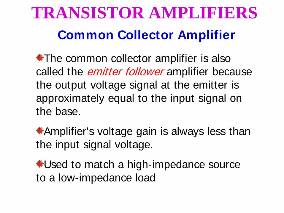
TRANSISTOR AMPLIFIERSCommon Collector Amplifier
The common collector amplifier is also called the emitter follower amplifier because the output voltage signal at the emitter is approximately equal to the input signal on the base.
Amplifier's voltage gain is always less than the input signal voltage.
Used to match a high-impedance source to a low-impedance load

TRANSISTOR AMPLIFIERSCommon Collector Amplifier
Common collector amplifier has a large current and power gain, excellent stability and frequency response.
The output impedance of this circuit is equal to the value of the emitter resistor, this circuit is used for impedance matching.
The input and output signals are in phase.

TRANSISTOR AMPLIFIERSCommon Collector Amplifier
Uses degenerative or negative feedback.
Degenerative feedback is the process of returning a part of the output of an amplifier to its input in such a manner that it cancels part of the input signal.
As a result, the common collector amplifierhas a voltage gain of less than 1.

TRANSISTOR AMPLIFIERSCommon Collector Amplifier
TRANSISTOR AMPLIFIERSCommon Collector Amplifier
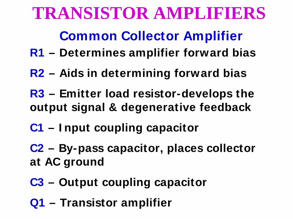
R1 – Determines amplifier forward bias
R2 – Aids in determining forward bias
R3 – Emitter load resistor-develops the output signal & degenerative feedback
C1 – Input coupling capacitor
C2 – By-pass capacitor, places collector at AC ground
C3 – Output coupling capacitor
Q1 – Transistor amplifier

TRANSISTOR AMPLIFIERSCommon Collector Amplifier
As the voltage on the base goes in a positive direction, the voltage on the emitter goes in a positive direction.
This positive voltage reverse biases the transistor decreasing ICresulting in an increase voltage drop across the transistor.

TRANSISTOR AMPLIFIERSCommon Collector Amplifier
As the voltage drop across the transistor increases the voltage drop across the load resistor R3 decreases, thus gain less than one.

TRANSISTOR AMPLIFIERS
Appraisal

TRANSISTOR AMPLIFIERS
1. In the common emitter configuration, the input is applied to the _______ and the output is taken from the ______ .
a. emitter; collector
b. base; collector
c. emitter; base
d. base; emitter

TRANSISTOR AMPLIFIERS
2. What is the purpose of resistors R1 and R2?
a. Amplify the input signal
b. Develop the output signal
c. Develop forward bias voltage for Q1
d. Block DC from the base of Q1

TRANSISTOR AMPLIFIERS
3. In a common collector amplifier, degenerative feedback is ______ out of phase with the input signal.
a. 0 degrees
b. 90 degrees
c. 180 degrees
d. 270 degrees

TRANSISTOR AMPLIFIERS
4. The common base amplifier has a voltage gain ______, but a current gain ______ .
a. less than one, less than one
b. greater than one, less than one
c. less than one, greater than one
d. greater than one, greater than one

TRANSISTOR AMPLIFIERS
5. In the common emitter configuration, R3 primarily affects
a. gain.
b. forward bias.
c. degeneration.
d. temperature stabilization.

TRANSISTOR AMPLIFIERS
6. What is the purpose of R4 in the common base amplifier?
a. Couple the output signal
b. Develop the input signal
c. Develop the output signal
d. Keep the base at AC ground

TRANSISTOR AMPLIFIERS
7. In the amplifier circuit shown, the purpose of C2 is to
a. couple the output signal.
b. develop the output signal.
c. place the collector at AC ground.
d. provide regenerative feeback.

TRANSISTOR AMPLIFIERS
8. The amplifiers class of operation is determined by
a. fidelity.
b. efficiency.
c. output waveform.
d. amount of forward bias.

TRANSISTOR AMPLIFIERS
9. With a transistor amplifier operating in class B, the collector current will flow for _____ of the input signal.
a. 90 degrees
b. 180 degrees
c. 360 degrees
d. more than 180 degrees but less than 360 degrees

TRANSISTOR AMPLIFIERS
10. In the transistor amplifier shown, what is the phase relationship between the input and output signals?
a. 0 degree phase shift
b. 90 degree phase shift
c. 180 degree phase shift
d. 270 degree phase shift

TRANSISTOR AMPLIFIER TEMPERATURE STABALIZATION

The process of minimizing undesired changes in a
transistor circuit caused by heat is called temperature
stabilization.
TEMPERATURE STABALIZATIONPURPOSE

Negative Temperature Coefficient
Transistors have a negative temperature coefficient
This means that as temperature increases the resistance of the transistor decreases.
TEMPERATURE STABALIZATION

Negative Temperature Coefficient
To compensate for temperature changes, all thermal stabilization circuits do the opposite to the transistor. As temperature increases, the thermal stabilization circuits reduce forward bias of the transistor, increasing its resistance.
TEMPERATURE STABALIZATION

TEMPERATURE STABALIZATIONCollector Current (IC) vs.Temperature Graph
Non-stabilized circuits
As temperature increases IC increases due to the resistance of the transistor decreasing.
This causes the transistor IC to move above its operating point.

TEMPERATURE STABALIZATIONSwamping Resistor Stabilization

TEMPERATURE STABALIZATIONSwamping Resistor Stabilization
Placing a resistor (R3) in the emitter for temperature stabilization is referred to as a “Swamping” resistor. Using swamping resistor (R3) for temperature stabilization results in degeneration feedback.
An increase in IC flows through the emitter resistor and develops an increase in voltage on the emitter.
This voltage opposes forward bias and reduces IB and IC.

TEMPERATURE STABALIZATIONSwamping Resistor with Bypass
Capacitor

TEMPERATURE STABALIZATIONSwamping Resistor with Bypass Capacitor
C2 is referred to as the “emitter bypass capacitor”.
By placing a large capacitor (C2) across R3, a signal ground is established and compensates for signal degeneration

TEMPERATURE STABALIZATIONThermistor Stabilization

TEMPERATURE STABALIZATIONThermistor Stabilization
A thermistor has a negative temperature coefficient of resistance.Bias is established by R1 and RT1 the thermistor.As temp. increases, resistance of RT1decreases, causing bias and IC to decreaseThis compensates for the change in IC due to temp. variations.
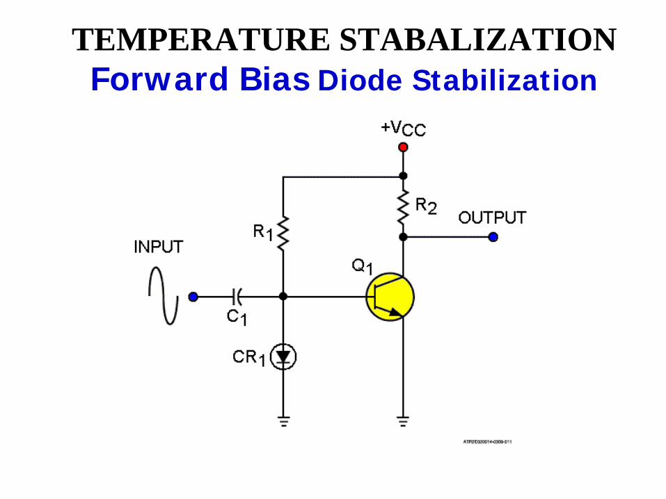
TEMPERATURE STABALIZATIONForward Bias Diode Stabilization
.

TEMPERATURE STABALIZATIONForward Bias Diode Stabilization
To more closely follow resistance changes of the transistor, replace the thermistor with a diode.
Diodes and transistors are made of the same materials, therefore, closely follow temperature changes.
As the amplifiers forward biased diode temperature increases its resistance decreases, thus forward bias decreases.

TEMPERATURE STABALIZATIONReverse Bias Diode Stabilization

TEMPERATURE STABALIZATIONReverse Bias Diode Stabilization
Used to reduce the effects of ICB on collector current.
As the reverse current of CR1 increases, it will cause a larger voltage drop across R1.
This will reduce the voltage across the base-emitter junction (VEB), causing base current to decrease, causing collector current will decrease.
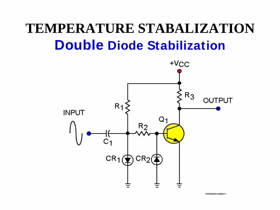
TEMPERATURE STABALIZATIONDouble Diode Stabilization

TEMPERATURE STABALIZATIONDouble Diode Stabilization
Forward biased diode CR1 compensates for changes in the resistance of the forward biased emitter-base junction due to temperature.
The reverse biased diode CR2compensates for the effects of ICB in the reverse biased collector-base junction.

TEMPERATURE STABALIZATIONHeat Sink
Heat sinks dissipate heat generated by high current through transistors
The transistor is connected directly to the heat sink and the fins dissipate the heat away from the junctions.

TEMPERATURE STABILIZATION
Appraisal
TEMPERATURE STABILIZATION
11. The “negative temperature coefficient” of a thermistor means that as temperature increases resistance ________ .
a. increases
b. decreases
c. Remains the same

TEMPERATURE STABILIZATION
12. Using the swamping resistor for thermal stability, what type of feedback is developed to control the amplifier?
a. Regenerative
b. Degenerative
c. Positive feedback

TEMPERATURE STABILIZATION
13. Which of the following devices is used to dissipate heat into the air?
a. Heat sink
b. Circuit board
c. Swamping resistor
d. Coupling capacitor
TRANSISTOR AMPLIFIER COUPLING

TRANSISTOR AMPLIFIER COUPLING
Purpose:
To achieve the high gain needed by most circuits, amplifiers are connected in series (or cascaded together) to form cascade amplifiers. The signal is couple from one amplifier stage to another.

TRANSISTOR AMPLIFIER COUPLING
Low gain amplifiers do not amplify the input signal enough to be of practical use. Using cascade amplifiers, high gain is achieved without incurring distortion.
The overall gain of a cascade amplifier is equal to the product of the individual gains, or: AV(TOTAL) = AV1 x AV2 x AV3
Cascade Amplifier Voltage Gain

TRANSISTOR AMPLIFIER COUPLINGCascade Amplifier Voltage Gain
The overall gain for this cascade amplifier, however, is 1000 (AV(TOTAL) = AV1 x AV2 x AV3 = 10 x 10 x 10 = 1000).

TRANSISTOR AMPLIFIER COUPLING
There are numerous types of circuits used to connect (or couple) one amplifier to another. The most commonly used are:
Direct Coupling
RC Coupling
LC Coupling
Transformer Coupling

Direct, RC, LC, and Transformer Coupling

LOW FREQUENCY GAIN LOSS
Three types of components cause low frequency gain loss in a cascade amplifier: coupling capacitors, inductors and transformers.
Coupling Capacitors cause low frequency gain loss because of their high capacitive reactance at low frequencies.
Inductors and Transformers cause low frequency gain loss at low frequencies for the opposite reason. They have low reactance at low frequencies.

Ø Components that cause high frequency gain loss are transistors, inductors and transformers.
Ø Stray capacitance caused by various wires and components will also cause high frequency gain loss.
HIGH FREQUENCY GAIN LOSS

Transistors - Interelement Capacitance
The emitter-base and collector-base junctions form an effective capacitance at high frequencies.
The signal bypasses the transistor thus preventing amplification.
Interelement capacitance causes loss of signal at high frequencies.
HIGH FREQUENCY GAIN LOSS

HIGH FREQUENCY GAIN LOSS
Inter-winding Capacitance
High frequency loss is due to inter-winding capacitance in which the individual coils can act as capacitors.
Only occurs at very high frequencies.

HIGH FREQUENCY GAIN LOSS
Stray Capacitance
Capacitance which exists between circuit components and wiring. The stray capacitance between two conductors could cause output signal amplitude to decrease.
Stray capacitance is not normally a problem in audio amplifiers. The highest frequency involved is about 20kHz and the capacitive reactance is still high.

DIRECT COUPLING
Note: The line connected between Q1collector and Q2 base enables AC and DC to be transferred from Q1 to Q2.
Direct coupling is the only type of coupling that can amplify DC voltages as well as AC signals.

DIRECT COUPLING
Has a poor high frequency response due to interelement capacitance of transistors.
R3 - Collector load resistor for Q1 and the base bias resistor for Q2.

Observe the loss of signal at the high frequencies which is due to the transistor’s inter-element capacitance.
DIRECT COUPLINGFrequency Response Graph
high frequency loss

When amplifying AC signals, direct coupling is normally used to amplify the audio range of frequencies (20Hz to 20kHz).
DIRECT COUPLINGFrequency Response Graph
high frequency loss

Resistive-Capacitive (RC)
RC coupling uses a capacitor to couple the signal between stages.
C2 – Passes AC and blocks (isolates) direct current between stages.

Resistive-Capacitive (RC)
Has a poor high frequency response due to transistor interelement capacitance.
Poor low frequency response due to XCof the capacitor.

Low frequency loss due to the high reactance of C1, C2and C3
High frequency loss due to the interelement capacitance of Q1and Q2
Resistive-Capacitive (RC)
low frequency loss
high frequency loss
Frequency Response Curve

LC coupling is used to amplify much higher frequencies.
RL is replaced with an inductor.
The gain of the amplifier is now determined by the inductor’s inductive reactance (XL).
Impedance Coupling (LC)

The main disadvantage of impedance coupling is that it is limited to high frequency use.
The reactance of the inductor at low frequencies is not large enough to produce good voltage gain.
Impedance Coupling (LC)

Frequency Response Curve
Loss of amplitude at low frequency is due to low reactance of the inductor.
Loss of amplitude at high frequency is due to inter-element capacitance of Q1 and Q2.
Impedance Coupling (LC)
low frequency loss high frequency
loss

Frequency Response Curve
The specific point (in this case 30MHz) that the amplifier will peak at is determined by the resonant frequency of the LC circuit.
Impedance Coupling (LC)
low frequency loss high frequency
loss

Transformer Coupling
The advantages of transformer coupling is that it provides isolation between stages so that one stage does not feedback and interfere with another stages, and is also used for impedance matching between stages.

Has a poor low frequency response due to low XL of transformer windings.
Transistor interelement capacitance and inter-winding capacitance of the transformer causes high frequency loss.
Transformer Coupling
Frequency Response Curve
low frequency loss
high frequency loss

TRANSISTOR AMPLIFIER COUPLING
Appraisal
TRANSISTOR AMPLIFIER COUPLING
14. What type of amplifier coupling is used that can amplify DC voltages as well as AC signals?
a. LC
b. RC
c. Direct
d. Transformer

TRANSISTOR AMPLIFIER COUPLING
15. What type of amplifier coupling is used for impedance matching and circuit isolation?
a. LC
b. RC
c. Direct
d. Transformer

TRANSISTOR AMPLIFIER COUPLING
a. C1, C2, and C3
b. R1 and R4
c. R2 and R5
d. Q1 and Q2
16. In the RC coupled amplifier, the low frequency gain loss is due to the reactance of components

TRANSISTOR AMPLIFIER COUPLING
a. C1, C2, and C3
b. R1 and R4
c. R2 and R5
d. Q1 and Q2
17. In the RC coupled amplifier, the high frequency gain loss is due to the inter-element capacitance of components

TRANSISTOR AMPLIFIER COUPLING
a. LC
18. In the following figure, what type of coupling is used between Q3 and Q4?
b. RC c. Direct d. Transformer

Appraisal Answers1. B
2. C
3. C
4. B
5. A
6. B
7. C
8. D
9. B
10. A
11. B
12. B
13. A
14. C
15. D
16. A
17. D
18. A

The End


![Welcome [images10.newegg.com]...or cigarette smoke may contaminate optical components, shortening the projector’s life span and darkening the image. - Locations near fire alarms](https://img.pdfslide.us/doc/110x75/5f04d31a7e708231d40fe46b/welcome-or-cigarette-smoke-may-contaminate-optical-components-shortening.jpg)


![Index [images10.newegg.com]images10.newegg.com/UploadFilesForNewegg/itemintelligence/UNITEC… · Index Index ... pressing function-key in your application program while the barcode](https://img.pdfslide.us/doc/110x75/5af4efbf7f8b9a4d4d8e5a53/index-index-index-pressing-function-key-in-your-application-program-while.jpg)