Embed Size (px)
Citation preview

Transient Modeling of Z-Source Chopper with and without ESR used
for Control of Capacitor Voltage BYAMAKESH NAYAK
1, SASWATI SWAPNA DASH
2
1Department of Electrical Engineering,
2Department of Electrical Engineering
KIIT University1, YMCA University of science and technology
2
1Bhubaneswar,odisha
2Faridabad,Haryana
INDIA [email protected]
2
Abstract: - The newly proposed Z-source chopper with two controlled switches is used to stabilize the duty
cycle above 0.5 is presented. The device has boost capability without polarity reversal in the range of duty
cycle 0 to 0.5 and buck-boost capability with polarity reversal of output voltage in the range of duty cycle 0.5 to
1. The above capabilities of the topology are studied through simulation. This paper also presents transient
modeling of the proposed Z-source chopper with and without ESR (equivalent series resistance). The effects of
ESR are studied in depth and based upon the transient modeling; the dc-link voltage is controlled by direct
measurement of capacitor voltage and inductor current. The presence of RHP (right-half-plane) zero in
developed average control-to-output model reveal that the output decreases initially before rising toward its
new steady-state value when a step increase in control input is applied. The non-minimum-phase transient
response can be reduced by proper feed-back control technique. Compensator for both voltage mode and
current mode control are designed using classical control technique through small-signal-analysis. Hysteresis
band modulator is used for finding out the switching function of switches. Performance of control method of
the compensated Z-source chopper is verified by simulation.
Key-Words: - Z-source chopper, Current mode control (CMC), Hysteresis band modulator, Buck-Boost
capabilities, Non–minimum–phase transient response, ESR (Equivalent series resistance), RHP (Right-half-
plane).
1 Introduction
Nowadays there is a rapid development in the
field of various applications of power electronics.
The previous literatures on Z-source chopper uses
only one controlled switch and other one is diode.
With one controlled switch and one uncontrolled
switch, the control range of duty cycle period is
limited to 0.5, because of diode will remain on the
entire period, if the duty cycle is above 0.5.Since the
duty cycle period is limited to 0.5,the circuit can be
only boost mode capability without polarity
reversal. The previous literatures only deal with one
controlled switch and diode with inductors and
capacitors arranged in X shape to boost up the
output voltage with polarity same as the input
voltage using shoot through technique [1] and the
performance analysis is done [2]. The duty cycle
period of previous literature circuit is limited to 0.5,
because of, above 0.5 the diode is forward biased
and therefore it remains on for whole the period
makes the circuit unstable. The unstable range of
duty cycle period can be eliminated using controlled
switch instead of diode so the output voltage can be
controlled by controlling the duty period range from
0 to 1. This paper now presents
the newly proposed Z-source chopper with battery
as input that can be used for both buck and boost the
input voltage. A simplified equivalent model of Z-
source with R-L load is shown in Fig-1.
Fig 1: Circuit diagram of Z-source chopper with
ESR of inductance and Capacitance
The newly proposed Z-source chopper is new
single-stage electronics power converter utilizing
impedance network with two controlled switches in
such a way that voltage-boost capability without
polarity reversal and boost-buck capability with
polarity reversal are achieved by introducing shoot-
through across the load. The above both voltage-
buck and boost capability feature of Z- source
s
SW2
S w 1
L
R l
R c
R a
L a
C
C
R c
L
R l
V g
i 1
i l
i l
i c
+
+
-
-
+
-
+
-
+
L
-
+
-
+
-
+
-
WSEAS TRANSACTIONS on CIRCUITS and SYSTEMS Byamakesh Nayak, Saswati Swapna Dash
E-ISSN: 2224-266X 175 Volume 13, 2014

converter can be used in fuel energy conversion
system and four quadrant speed control of dc motor
drive system. The effect of parasitic component of
inductor and capacitor are studied in detail. The
battery-side phenomenon is associated with the
value of inductance and capacitance in X shaped
network, and is studied using small-signal analysis
to show the presence of the right-half-plane (RHP)
zero in the control-to-load current, control-to-
inductor current and control-to-voltage transfer
functions [3],[4]. Transient modeling of Z-source
converter with R-L load is analyzed through state-
space average analysis method to show its non-
minimum-phase response caused by battery-side [5],
[6], [7]. The passive parameters such as inductor
and capacitor are selected based on ripple current
and ripple voltage respectively by considering worst
case condition. Dynamic modeling of Z-source with
R-L load has been formulated using state-space
averaged analysis method. Small signal model has
been derived from the state-space averaged dynamic
method for linearization. Based on small signal
linearization model the control law for output
voltage control is derived. Output voltage is
controlled by direct measurement of the voltage and
inductor current. The compensators for the voltage
loop and the current loop are designed based on the
frequency responses and as well as root locus
technique. A hysteresis band modulator is used for
improving transient response and tested in
MATLAB/SIMULINK simulation using an efficient
closed loop Z-source switching -functional model.
2 State-space Averaged Analysis of Z-
source Chopper with R-L load
Operation of Z-source chopper with R-L load can be
explained in two modes. Assuming continuous
conduction mode, there are two modes one is called
shoot through mode, where load is shorted by
turning on the switch-1 and other is input connected
mode where switch-1 is on to connect the input to
load. As shown in Fig1, this converter has three
energy storage elements so three state variables are
needed to represent state-space model of Z-source
chopper. The ESR (equivalent series resistance) of
inductor and capacitor are taken into consideration
for formulating state-space average model of Z-
source chopper. The KVL, KCL expressions in
terms of the inductor current, load current and
capacitor voltage when switch-1 is on (switch-2 is
off) are:
(1)
(2)
(3)
Where Rl and Rc represent ESR of inductance (L),
ESR of capacitance(C) of X shaped network of
chopper circuit. Ra and La is the load to z-source
chopper.
The (1), (2) and (3) can be represented in state-space
form as:
= and
Where,
, then
Where
And (4)
Similarly when switch-1 is off mode and the switch-
2 is conducting mode, the equations can be written
based on KCL and KVL as:
(5)
WSEAS TRANSACTIONS on CIRCUITS and SYSTEMS Byamakesh Nayak, Saswati Swapna Dash
E-ISSN: 2224-266X 176 Volume 13, 2014
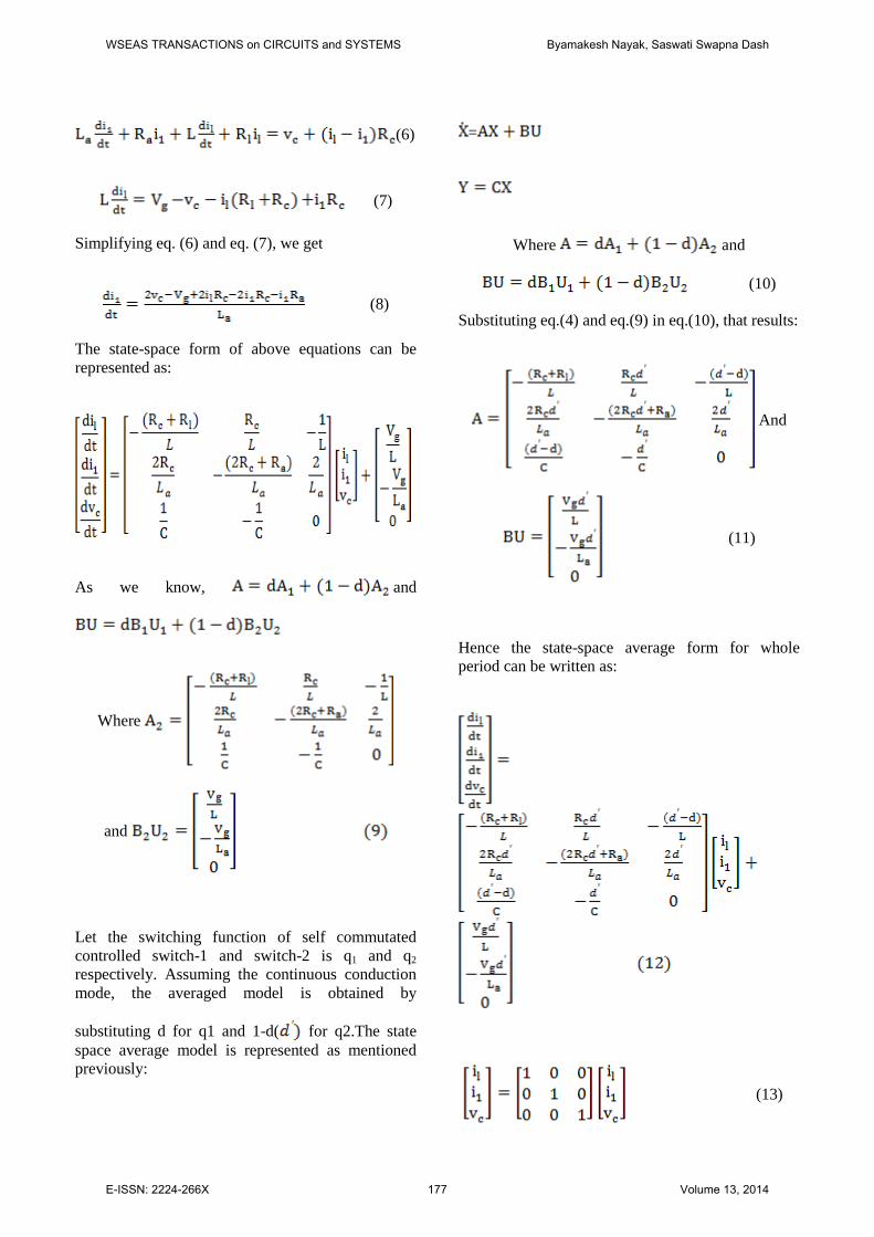
(6)
(7)
Simplifying eq. (6) and eq. (7), we get
(8)
The state-space form of above equations can be
represented as:
As we know, and
Where
and
Let the switching function of self commutated
controlled switch-1 and switch-2 is q1 and q2
respectively. Assuming the continuous conduction
mode, the averaged model is obtained by
substituting d for q1 and 1-d( for q2.The state
space average model is represented as mentioned
previously:
=
Where and
(10)
Substituting eq.(4) and eq.(9) in eq.(10), that results:
And
(11)
Hence the state-space average form for whole
period can be written as:
(13)
WSEAS TRANSACTIONS on CIRCUITS and SYSTEMS Byamakesh Nayak, Saswati Swapna Dash
E-ISSN: 2224-266X 177 Volume 13, 2014

3 Small Signal Analysis The state-space averaged model of Z-source
converter with R-L load shown in (12) has non
linear in nature as the control parameter (d) is in
matrix A. Therefore small signal analysis is required
to make the state-space to be linear. Due to small
variation of in steady state D the state variables
are changed to , , .The
state-space averaged model (12) and (13) with small
perturbation is modified as:
(14)
(15)
Subtracting steady-state representation of (12) from
(14) and (13) from (15) neglecting higher order
perturbation terms, the small signal model is:
(16)
(17)
4 Steady State Analysis and Design
Consideration
The steady state equations can be derived from
averaged state-space model (12) by simplification
and represented as:
(18)
(19)
Where
Under ideal condition (assuming ESR of inductance
and capacitance is zero) then A=0; B=Ra (2D-1),
which gives:
(20)
Selections of passive parameters of X shaped
network are based on minimization of current
ripples and voltage ripples. It is also shown that the
change of passive parameters affect the transient
responses. It is therefore important to carefully
select the Z-source L and C values to achieve a good
compromise between oscillatory response, ripple
factor and non minimum phase effect. Initially
selection is based on ripple factor. A battery of 12V
input is used in Z-source chopper to control the
voltage across the load resistor. Let us assume that
the voltage across the load of R (10Ω) is increased
to 5 times (60V).The load current is =6A. At rated
voltage operation the voltage gain of Z-source
chopper is found to be 5 (60/12) and hence D is
calculated from (20) under ideal condition and
found to be D=0.445 for 60V and .545 for 60V
with A. Let the current ripple of and the
capacitor voltage ripples ( ) are assumed to be
WSEAS TRANSACTIONS on CIRCUITS and SYSTEMS Byamakesh Nayak, Saswati Swapna Dash
E-ISSN: 2224-266X 178 Volume 13, 2014

maximum limit of , then
and V.Assuming the operation of switch
with switching frequency of 10KHz under full rated
voltage condition, when the switch 2 is on for a
period of (1-D)T second, then the inductor is
calculated as: -(-60) and
then L =5.4mH, Hence choose
mH.Similarly the value is calculated by
considering the switch1 in off condition using the
equation (3), which gives C=1.375mF
(approximately).
The ESR of capacitor depends on switching
frequency and capacitance value of capacitor. The
mathematical expression of ESR of capacitor is:
The ESR effect of capacitor is negligible if the
switching frequency is very high. The ESR of
inductance depends on number of turns, diameter of
wire and also switching frequency. The ESR of
inductance increases with increase in frequency.
The ESR sensitivity effect is shown in Fig 2.The
boost capability decreases with increase the ESR
value of capacitance and also inductance. The ESR
value of inductance is more dominant to decreases
the boost capability of Z-source converter compared
to ESR value of capacitor. From the figures, it is
also found that the Z-source chopper posses boost
capability with same polarity as input in the duty
ratio range between 0<D<0.5 and both boost and
buck capability with reverse polarity in the duty
ratio range between 0.5<D<1.
0 0.1 0.2 0.3 0.4 0.5 0.6 0.7 0.8 0.9 1-20
-15
-10
-5
0
5
10
15
20
Ideal Condition
RL=0.02 and RC=0ohm
RL=0.1 and RC=0ohm
Boost ModeBuck and Boost mode with
polarity reversal
0 0.1 0.2 0.3 0.4 0.5 0.6 0.7 0.8 0.9 1-20
-15
-10
-5
0
5
10
15
20
Ideal condition
RC=0.02 and RL=0ohm
RC=0.1 and RL=0ohm
Fig 2 (a, b): Voltage gain versus duty cycle of Z-
source chopper with and without ESR of inductance
and Capacitance.
The transfer functions (21), (22) and (23) are
derived from small signal model given in (16) and
(17) at D=0.4 using the parameters as given in
Table 1.here in table 1 the parameters are justified
from the Simulink model.
Table 1
Vg Ra RL
(ESR)
L La C RC
(ESR)
12V 10
Ω
0.02 Ω 4
mH
2
mH
1.375
mF
0.12 Ω
WSEAS TRANSACTIONS on CIRCUITS and SYSTEMS Byamakesh Nayak, Saswati Swapna Dash
E-ISSN: 2224-266X 179 Volume 13, 2014

(21)
(22)
(23)
Where is denoted
as control-to-inductor current, control-to-load
current, control-to-capacitor voltage transfer
functions respectively.
5 Transient Analysis Before attempting the closed loop control of Z-
source chopper it is necessary to study the transient
behaviour which depends on passive parameters and
its ESR value. To date, many methods for modeling
of power converters have been reported in the
literature[6]-[9].Here commonly adopted average
state space analysis with small signal method is
used to study the transient behaviour of open loop
system with step changes of duty cycle.
-100 -80 -60 -40 -20 0-500
-400
-300
-200
-100
0
100
200
300
400
500
Pole trajectories of control-to output transfer function
with change in D (ideal case)
D=0
D=0.5
D=1
-100 -80 -60 -40 -20 0-500
-400
-300
-200
-100
0
100
200
300
400
500
Pole trajectories of control-to output transfer function
with change in D (ESR of capacitance = 0.1ohm)
D=0
D=0.5
D=1
Fig 3 (a, b): Pole trajectories of Z-source chopper
with and without ESR Capacitance.
To control the wide range of output voltage, it is
important to study the movements of poles and zero
in order to maintain acceptable performance and
stability[10]-[15]. Fig 3(a, b) shows the poles
trajectories of control-to output transfer function
with change in D from 0 to 1 with and without the
ESR value. Under ideal case (without ESR) the one
of the pole is lying on the real axis and is far away
from the imaginary axis and therefore the effect of
this pole is negligible in transient response.
Therefore under ideal condition the system analysis
can be easily controlled by considering the system
as a second order system [16], [17]. The effect of
ESR is shown in the figure. The one of the pole
which is far away from the imaginary axis under
ideal case is moving towards the imaginary axis and
the movement speed depends upon the value of
ESR. The other two poles moves slightly away from
the imaginary axis. All the three poles are the
dominant poles and have impact on the transient
response particularly in the range of D from 0.4 to
0.7. The movement of poles away from imaginary
axis and one pole which is far away from the
imaginary axis moves towards the imaginary axis
due to ESR improves the transient response. The
overshoot and undershoot are reduced, which
reduces the system damping and also settling time.
Thus with ESR the transient responses are improved
but the boost capability of system is greatly reduced
with increase in ripples and incurred more loss in
system. The above conclusions are observed by
simulating the Z-source chopper by step changing
the D from 0.3 to 0.4 and 0.7 to 0.6.The simulated
WSEAS TRANSACTIONS on CIRCUITS and SYSTEMS Byamakesh Nayak, Saswati Swapna Dash
E-ISSN: 2224-266X 180 Volume 13, 2014

responses of control-to-capacitor voltage, control-
to-inductor current and control-to-load current
during step change in D from 0.3 to 0.4 and 0.7 to
0.6 are shown in Fig.(5) and Fig.(6) respectively.
0 50 100 150 200 250 300 350 400-400
-300
-200
-100
0
100
200
300
400
real axis
Imagin
ary
axis
RHP Zero trajectories under ideal condition with change in D
D=0D=0.5
D=.9
0 2000 4000 6000 8000 10000 12000 14000-1
-0.8
-0.6
-0.4
-0.2
0
0.2
0.4
0.6
0.8
1
Real axis
Imagin
ary
axis
RHP Zero trajectories of capacitor voltage under ideal condition with change in D
D=0
D=1
D=0.5
D=0.5
-50 0 50 100 150 200 250 300 350 400-400
-300
-200
-100
0
100
200
300
400
Real Axis
Imagin
ary
Axis
RHP Zero trajectories of load current with ESR (RC=0,1 ohm and RL=0 ohm)
with change in D
D=0.4 D=0.2
D=0.8
D=0.6
D=0.6
D=0.8
D=0
D=0.9
D=0.9
0 2000 4000 6000 8000 10000 12000 14000-1
-0.8
-0.6
-0.4
-0.2
0
0.2
0.4
0.6
0.8
1
RHP Zero of capacitor voltage with ESR (RC=0.1ohm and RL=0 ohm
with change in D
Real Axis
Imagin
ary
axis
D=0D=0.2
D=0.8D=0.6
D=0.4
D=0.9
Fig 4 (a, b, c, d): RHP Zero trajectories of Z-source
chopper of load current and capacitor voltage with
and without ESR.
It is necessary to study the non-minimum phase
effect of control-to-output transfer functions with
and without ESR to analysis the dip caused during
sudden change in the step command. As shown in
Fig.(4),the control-to-load current and control-to-
capacitor voltage transfer functions posses the non-
minimum-phase transient because of presence of
zero in right side of S plane (RHP zero) whereas
control -to- inductor current transfer function has
non-minimum-phase transient. Due to non-
minimum phase effect of control-to-inductor current
transfer function, the dip in transient response is
zero at the instant of step increase in D and it is
confirmed by Fig.5 (b).The dip will be created in
control-to-load current and control-to-capacitor
voltage transfer functions at the instant of step
increase in D because of the presence of Zero in
right side of S plane. The RHP zero movement of
control-to-load current and control-to-capacitor
voltage transfer functions due to change in D with
and without ESR are shown in Fig(4).The
movement of RHP zero towards imaginary axis is
faster with increase of ESR value as compared to
ideal condition (without ESR) especially, in the
range of D from 0.3 to 0.6. Therefore The increase
of ESR value of X network of Z-source chopper
increases the non- minimum-phase undershoot
(created large dip at the instant of change in D) . For
illustrating the non–minimum-phase undershoot of
the different transfer functions of Z-source chopper,
an initial condition of D=0.3 and 0.7 are assumed.
With step change of D from 0.3 to 0.4 at .4 second
and 0.7 to 0.6 at 1second, the simulations are carried
out in Matlab/simulink environment by taking
MOSFET as controlled switch.Fig.5(a,b,c) and
Fig.6(a,b,c,) show the step responses of control-to-
WSEAS TRANSACTIONS on CIRCUITS and SYSTEMS Byamakesh Nayak, Saswati Swapna Dash
E-ISSN: 2224-266X 181 Volume 13, 2014

capacitor voltage, control-to-inductor current and
control-to-load current respectively with and
without ESR. The figure of control-to-capacitor
voltage, control-to-load current clearly shows that
there is a large dip of load current and capacitor
voltage as compared to ideal condition at the instant
of transient before rising the towards their new
steady-state values non-minimum-phase features for
RHP zero. It is proved by other researcher that the
increase of inductance of X network of Z-source
parameters increases the system damping with a
reduced overshoot and undershoot but an increased
rise time and settling time due to shifting of
dominant poles toward the origin of complex
plane[7]. The increase of inductance of X network
of Z-source parameters increases the non-
minimum-phase undershoot due to shifting of RHP
zero toward the origin of complex plane, whereas
the increase of capacitance has negligible effect on
non-minimum-phase undershoot of load current and
capacitor voltage[7].
It is therefore concluded that the Shifting of RHP
zero towards imaginary axis due to ESR value
increases non-minimum-phase undershoot, whereas
movement of one of the poles towards imaginary
axis decreases the system settling time and
oscillatory response. Further with increase of ESR
value decreases the boost capability of Z-source
chopper and introduce large ripple in output signal.
For a more effective implementation of feedback
control for boosting operation of Z-source chopper
for voltage control, it is recommended that instead
of armature current feedback ,the inductor current
feedback can be used, which eliminate the non-
minimum-phase effect. In this paper the
compensators design are explained in next
subsection by taking the inductor current feedback.
0 0.1 0.2 0.3 0.4 0.5 0.6 0.7 0.80
5
10
15
20
25
30
35
40
45
Time (second)
Capacitor
Voltage in V
olt.
Simulated response of Z-source chopper of capacitor voltage
during step change in D from 0.4 to 0.4
Ideal Condition
With ESR
Initial dip at starting
0 0.1 0.2 0.3 0.4 0.5 0.6 0.7 0.8-2
0
2
4
6
8
10
12
14
16
Time (second)
Inducto
r C
urr
ent
In A
mp.
Simulated response of Z-sorce chopper of inductor current
during step change in D from 0.3 to 0.4.
Ideal Condition
With ESR
0 0.1 0.2 0.3 0.4 0.5 0.6 0.7 0.8-1
0
1
2
3
4
5
Simulated response of Z-source chopper of load current
during step change in D from 0.3 to 0.4.
Time (second)
Load C
urr
ent
In A
mp.
Ideal condition
With ESR
Initial dip at starting
Fig 5 (a, b, c): Simulated response of Z-source
capacitor voltage, inductor current and load current
during a step change in D from 0.3 to 0.4
respectively.
0 0.2 0.4 0.6 0.8 1 1.2 1.4 1.6 1.8 2-35
-30
-25
-20
-15
-10
-5
0
5
Time (second)
Capacitor
Voltage I
n V
olt
Simulated response of Z-source chopper of Capacitor voltage
during step change in D from 0.7 to 0.6.
Ideal Condition1
With ESR
WSEAS TRANSACTIONS on CIRCUITS and SYSTEMS Byamakesh Nayak, Saswati Swapna Dash
E-ISSN: 2224-266X 182 Volume 13, 2014

0 0.2 0.4 0.6 0.8 1 1.2 1.4 1.6 1.8 2-4
-2
0
2
4
6
8
10
12
Simulated response of Z-source chopper of inductor current
during step change in D from 0.7 to 0.6.
Time (second)
Inducto
r C
urr
ent
In A
mp.
Ideal Condition
With ESR
0 0.2 0.4 0.6 0.8 1 1.2 1.4 1.6 1.8 2-4
-2
0
2
4
6
8
10
12
Simulated response of Z-source chopper of inductor current
during step change in D from 0.7 to 0.6.
Time (second)
Inducto
r C
urr
ent
In A
mp.
Ideal Condition
With ESR
Fig 6 (a, b, c): Simulated response of Z-source
capacitor voltage, inductor current and load current
during a step change in D from 0.7to 0.6
respectively.
6 Current Mode Control of Z-Source
Chopper
Fig 7: Circuit diagram of Z-source chopper with
feedback control circuit
The derived transfer functions from small signal
model can be used for current mode control method.
In current mode control method there are two loops
one is inner input current loop and other is outer
capacitor voltage loop where actual voltage follow
the reference voltage. In inner loop, the direct
measurement of inductor current is compared with
the reference inductor current estimated from the
outer loop.
Fig 8 : Block diagram of closed loop capacitor
voltage control.
The error is compensated using Hence the
loop transfer function of inner current loop is
.The switching function is
determined from the output of through
hysteresis band controller.In outer voltage loop, the
direct measurement of capacitor voltage is
compared with reference voltage. The error is
compensated using .The output of is
the inductor input current command which is
processed by actual current by inner loop. The block
diagram of current control mode is shown in Fig 8.
The outer loop is highly coupled with inner loop
because of inductor current command is generated
from outer loop which is the command value of
inner loop [4]. The coupling behavior can be
represented by transfer function is as follows:
(24)
Substituting the value of in eq.(24):
(25)
Solving eq.(25) and eq.(23) then inductor current
command-to-speed transfer function will be
HB
Gvcd(S)
Gild(S)
Vc
il d
HB Gild(S
)
il d
Gvcd(S)/
Gild(S)
WSEAS TRANSACTIONS on CIRCUITS and SYSTEMS Byamakesh Nayak, Saswati Swapna Dash
E-ISSN: 2224-266X 183 Volume 13, 2014

(26)
7 Compensator Design
Based on the small signal expressions of the Z-
source chopper the compensators blocks
are designed using the design
specifications given in Table-1without ESR. First,
the inner current loop compensator is designed
based on frequency response. The bode plot of
at D=.3 and .4 is given in Fig.9 (a,b) It can
be observed that the three closed loop poles are on
the negative side of real axis of the complex plane.
One of the closed loop pole is very close to
imaginary axis (-80) and other two poles are far
away from the imaginary axis (-1.5*104 ,-5*10
3 ).
The phase margin of open loop transfer function at
D=0.4 is 900 at gain cross over frequency 1.5*10
4
rad/s. It is also observed that the closed loop pole
which is near to the imaginary axis moves towards
the imaginary axis with increase in D up to 0.5
whereas the far away poles moves away from the
imaginary axis, which increases the gain cross over
frequency(7.5*103
at D=0.3 to 1.5*104 at D=0.4).
Since gain cross over frequency increases with
increase in D from 0 to 0.5 the band width is
increased, which causes high picking behaviours to
noise. In order to reduce the high picking
behaviours and band width, the PI compensator is
used in inner loop which act as low pass filter. The
root locus technique is used for design of
compensator to place the closed loop poles in order
to get best performances. From root locus diagram
the inner compensator is designed and found to be
(27)
The compensated bode diagram and root locus of
inner loop transfer function is shown in Fig.10.In
this design the gain crossover frequency is
decreased from 7.5*103
rad/sec to 4.5*103. It is
important to note that the inner loop must be must
faster than the outer loop to prevent any clashes
between the two loops [5]. In outer speed control
loop, the PI compensator is used to meet the
capacitor voltage to command duty ratio (d) value
with good transient response. Although it is difficult
to get desired transient performances such as
increase of speed behaviours, decrease of overshoot
and settling time by using any of the classical
compensators, because of all the poles are not
available for placing at desired location, but the
gains of fixed compensator are determined in such a
way that the non dominant poles are placed far away
from the dominant poles to reduce the transient
effects created by dominant poles. Here the
uncompensated system is unstable because one of
the closed loop pole is closed to origin but in right
side of S-plane. Hence lead compensator is used to
improve transient response and make it stable by
moving the unstable pole towards left half of S-
plane. The drawback of lead compensator increases
the steady state error. The gains of lead compensator
are selected based upon the trade-off between
transient response and steady-state error. The
selection of gains of compensator is carried out by
root-locus method and it is verified by bode diagram
using Control toolbox in MATLAB environment.
The bode diagram of uncompensated and
compensated loop transfer functions of speed loop
are shown in Fig.11and Fig.12 respectively. The
compensator for capacitor voltage loop used for
control of output voltage derived from root locus
tool box is expressed as:
(28)
100
101
102
103
104
-180
-90
0
90
P.M.: 89.7 deg
Freq: 7.51e+003 rad/sec
Frequency (rad/sec)
-20
0
20
40
60
G.M.: Inf
Freq: NaN
Stable loop
Open-Loop Bode Editor (C)
-8000 -6000 -4000 -2000 0-400
-300
-200
-100
0
100
200
300
400
Root Locus Editor (C)
Real Axis
WSEAS TRANSACTIONS on CIRCUITS and SYSTEMS Byamakesh Nayak, Saswati Swapna Dash
E-ISSN: 2224-266X 184 Volume 13, 2014

100
105
-180
-90
0
90
P.M.: 89.8 deg
Freq: 1.5e+004 rad/sec
Frequency (rad/sec)
0
10
20
30
40
50
60
G.M.: Inf
Freq: NaN
Stable loop
Open-Loop Bode Editor (C)
-15000 -10000 -5000 0-300
-200
-100
0
100
200
300
Root Locus Editor (C)
Real Axis
Fig 9 (a, b): Root locus and Bode plot of
uncompensated for CM control (Fig.9(a)
for D=0.3 and Fig.9(b) for D=0.4).
10-2
100
102
104
-180
-90
0
90P.M.: 89.5 deg
Freq: 4.7e+003 rad/sec
Frequency (rad/sec)
-20
0
20
40
60
G.M.: Inf
Freq: NaN
Stable loop
Open-Loop Bode Editor (C)
-6000 -5000 -4000 -3000 -2000 -1000 0-400
-300
-200
-100
0
100
200
300
400
Root Locus Editor (C)
Real Axis
Fig 10: Root locus and Bode plot of compensated
for CM control.
100
102
104
106
90
180
270
360
P.M.: 90 deg
Freq: 293 rad/sec
Frequency (rad/sec)
-60
-40
-20
0
20
G.M.: 9.08 dB
Freq: 2.75e+003 rad/sec
Unstable loop
Open-Loop Bode Editor (C)
-4000 -2000 0 2000 4000-3000
-2000
-1000
0
1000
2000
3000
Root Locus Editor (C)
Real Axis
Fig 11: Root locus and Bode plot of uncompensated
for capacitor voltage control
10-2
100
102
104
106
90
180
270
360
450
P.M.: 88.2 deg
Freq: 330 rad/sec
Frequency (rad/sec)
-40
-30
-20
-10
0
10
G.M.: 8.27 dB
Freq: 2.77e+003 rad/sec
Stable loop
Open-Loop Bode Editor (C)
-6000 -4000 -2000 0 2000 4000-3000
-2000
-1000
0
1000
2000
3000
Root Locus Editor (C)
Real Axis
Fig 12: Root locus and Bode plot of compensated
for capacitor voltage control
8 Simulation Results In order to verify the proposed control strategy of
current mode control technique used for capacitor
voltage control, simulations are carried out using
Matlab/Simulink software. The same circuit
parameters are used as in Table-1 without ESR. The
designed compensators gain using (27) and (28) are
used for inner loop and outer loop respectively. Step
responses of 36V for 2 second and at 2 second step
response command increased to 60V are used to
observe the dynamic characteristics of capacitor
voltage, inductor current, and load current
respectively. Fig 13 (a,b,c) shows the capacitor
voltage, inductor current, and load current responses
of change of step reference from 36 V to 60V
respectively. It has been observed that both of the
speed responses reach the respective steady state
value without exhibiting the oscillation. The settling
time for high capacitor voltage response is higher
than the low capacitor voltage step response
command. It can be observed from Fig-13(a) that
there is no dip in voltage response at the time of
starting of transient due to sudden change of
command speed from 36V to 60 V. Settling time for
36V is 0.5 second and for 60V it is about 0.9
second. The ripple of load current, which depends
upon hysteresis band controller and inductance of
the circuit, is found to be with average steady
value 3.5Ampere for low voltage step command of
36V and average steady state value of 6Ampere for
high Voltage reference of 60V.
WSEAS TRANSACTIONS on CIRCUITS and SYSTEMS Byamakesh Nayak, Saswati Swapna Dash
E-ISSN: 2224-266X 185 Volume 13, 2014

0 0.5 1 1.5 2 2.5 3 3.5 40
10
20
30
40
50
60
70
Time (second)
Capacitor
Voltage I
n V
olt.
Response Of Capacitor Voltage
Actual Response
Step Command
0 0.5 1 1.5 2 2.5 3 3.5 40
5
10
15
20
25
30
35
Time (Second)
Inducto
r C
urr
ent
In A
mp.
Response Of Inductor Current
0 0.5 1 1.5 2 2.5 3 3.5 4-2
-1
0
1
2
3
4
5
6
7
Time (Second)
Load C
urr
ent
In A
mp.
Response Of Load Current
Fig 13(a, b, c): Capacitor voltage, Inductor Current ,
Load Current responses of closed loop Z-source
chopper control of R-L load for a change of step
response from 36 V to 60 V.
9 Conclusion
This paper presents detailed transient analysis on Z-
source chopper with ESR effect used for capacitor
voltage control under R-L load using small signal
model. The study of transfer function of control -to-
output has revealed that the existence of RHP zero
which depend on ESR value of passive parameters
and control parameter mainly on load current and
capacitor voltage causes dip in output responses due
to sudden change of capacitor voltage command.
However, the dip in inductor current is zero because
of non existence of RHP zero as a result; the inner
feedback inductor current control is used to study
the closed loop capacitor voltage control instead of
load current feedback. The compensators for the
capacitor voltage loop and the current loop are
designed based on the frequency responses and as
well as root locus technique. The oscillation and
slower rise time can be improved by suitable design
of compensator and using hysteresis band controller.
The simulation responses of capacitor voltage, load
current and inductor current for boosting of voltage
are presented by suitable design of compensators.
References:
[1] F.Z.Peng, Z source inverter, IEEE Transactions
on Industrial Application, Vol.39, No.2, 2003,
pp.504-510.
[2] B.K.Nayak, Saswati Swapna Dash, Performance
Analysis of Different Control Strategies in Z-
source Inverter, ETASR-Engineering,
Technology & Applied Science Research, Vol.3,
No.2, 2013, pp.391-395.
[3] J.Liu, J.Hu, and L.Xu, Dynamic Modeling and
Analysis of Z Source Converter Derivation of
AC Small Signal Model and Design-Oriented
Analysis, IEEE Transactions on Power
Electronics, Vol.22, No.5, 2007, pp 1786-1796.
[4] F.Z.Peng, M.Shen, and Z.Quin, Maximum boost
control of Z-source inverter, IEEE Transactions
on Power Electronics, Vol.20, No.4, 2005, pp
883-838.
[5] Gokhan Sen and Malik Elbuluk,Voltage and
Current Programmed Modes in control of the Z-
Source Converter, IEEE Transactions on
Industry Applications, Vol-46, No. 2, 2010,
pp.680-686.
[6] C.J.Gajanayake, D.Mahinda and Poh.Chiang
Loh, Small-Signal and Signal-Flow-Graph
Modeling of Switched Z-source Impedance
Network, IEEE Power Electronics Letter, Vol.3,
No.3 2005.
[7] Poh.Chiang Loh, D.M.Vilathgamuwa,
C.J.Gajanayake and C.W.Teo, Transient
WSEAS TRANSACTIONS on CIRCUITS and SYSTEMS Byamakesh Nayak, Saswati Swapna Dash
E-ISSN: 2224-266X 186 Volume 13, 2014

Modeling and Analysis of Pulse-
width_modulated Z-Source Inverter, IEEE
Transactions on Power Electronics, Vol.22,
No.2, 2007, pp.498-507.
[8] F.Z.Peng, X.M.Yuan, X.P.Fang, and Z.M.Quin,
Z source inverter for adjustable speed drives,
IEEE Power Electronics Letter, Vol.1, No.2,
2003, pp.33-35.
[9] K.Smedley,and S.Cuk, Switching flow graph
nonlinear modelling technique, IEEE
Transactions on Power Electronics, Vol.9,
No.4, 1994, pp.405-413.
[10] R.D.Middlebrook and S.Cuk, A general
unified approach to modelling switching
converter power stages, IEEE PESC
proceedings, 1976,pp.18-34.
[11] P.T.Krein, Elements of Power Electronics,
New York:Oxford University Press,1998.
[12] G.F.Franklin, J.D.Powel and A.Emami-
Naeini, Feedback Control of Dynamic Systems,
MA:Addison-Wesley,1994.
[13] R. Aaron Kelvin, Noreen L. Foster,
Dannielle P. Hazel and A. M. Hasanul Basher,
Closed-loop position control system using
labview, Southeast conference, 2002, pp.283-
286.
[14] R.Krishnan, Electric motor drives modeling,
analysis and control, Pearson education
(singapore) pvt.ltd, 2003.
[15] L.Umanand, Power electronic essentials
and applications, Wiley publishers, 2009.
[16] B.K. Nayak and S. S. Dash, Transient
modeling of Z-source chopper used for
adjustable speed control of DC motor drive,
IEEE Fifth Power India Conference, 2012, pp.
1-6.
[17] B.K.Nayak, Saswati Swapna Dash, Battery
Operated Closed Loop Speed Control of DC
Separately Excited Motor by Boost-Buck
Converter, IEEE International conference on
power electronics (IICPE-2012), 2012.
WSEAS TRANSACTIONS on CIRCUITS and SYSTEMS Byamakesh Nayak, Saswati Swapna Dash
E-ISSN: 2224-266X 187 Volume 13, 2014