Embed Size (px)
Citation preview

Design And Layout Of 2KB SRAM Memory For 180nm Technology
Industrial Training Report
Submitted By
Pramod M (05EC78)
BACHELOR OF TECHNOLOGY
October 2008
Department of Electronics and Communication Engineering
National Institute of Technology KarnatakaSurathkal

1
1

Design And Layout Of 2KB SRAM MemoryFor 180nm Technology
Pramod M & Minkle Eldho Paul
June 2008
1Department of Electronics and Communication,National Institute of Technol-ogy Karnataka

Abstract
This report details the training in the area of Mixed Signal Design at SankalpSemiconductor,Hubli. The training involved lectures on Mixed Signal Designflow and basic circuit theory including operation on MOSFETs.This reportcontains the implementation of SRAM memory in 180nm technology andthe issues involved in layout design.The memory is implemented using Ca-dence tools namely Schematic-Composer,Virtuso,Assura.The access time formemory is intended to be within 20ns.

Acknowledgment
We would like to thank Mr.Vivek G Pawar,CEO,Sankalp SemiconductorPvt. Ltd. for accommodating us for the training. We thank Dr. Sri-pathi Acharya for his support and our special thanks to Prof. P Sub-banna Bhat for guiding us through the project. We would like to ex-tend our gratitude to Prabhat Agarwal, Venkatesh Puttur, Ajit.S, DamodarCharate,Vidyasagar T for their support and guidance in layout design. Wethank Department of Electronics and Communication,BVBCET for provid-ing us lab facility for working on the project.
1
Contents
1 Introduction 3
2 Mixed Signal Design flow 4
3 Project Definition 6
4 Memory Architecture 7
5 Design of Individual Modules 85.1 Bit Cell . . . . . . . . . . . . . . . . . . . . . . . . . . . . . . 85.2 Precharge . . . . . . . . . . . . . . . . . . . . . . . . . . . . . 95.3 Sense Amplifier . . . . . . . . . . . . . . . . . . . . . . . . . . 105.4 Write Circuit . . . . . . . . . . . . . . . . . . . . . . . . . . . 115.5 Column Decoder . . . . . . . . . . . . . . . . . . . . . . . . . 125.6 Row Decoder . . . . . . . . . . . . . . . . . . . . . . . . . . . 12
6 2KB SRAM Memory 23
7 Conclusion 24
2

Chapter 1
Introduction
The Semiconductor industry tries to catchup with Moore’s law by scaling thesize of the devices. Reduction in the size of the device guarantees reductionof its parasitic capacitances but,the parasitics of the metal interconnect be-comes dominant and the leakage current of the device becomes significantlylarge.A well designed layout of chip ensures better performance.
In a typical CMOS chip, nearly 90% of the chip area is occupuied by dig-ital circuits whereas only around 10% is occupied by analog.As more andmore discrete components get intergrated into the chip, its important thatthe interface between them is well defined. As an example consider a mo-bile phone that can play FM and mp3 and record videos. This requies aseparate RF module for FM reception,an mp3 decoder, DSP processor forvideo compression, a memory module to store the video, power managementunit to signal sleep and wake cycle and most importantly the RF module forhigh frequncy telephone signal tranception. All these modules if integratedon a PCB requires a lot of area and the mobile becomes clumsy and powerhungy. Integrating all the modules on a single chip saves power and henceit becomes compact and reliable.This nessasiates a robust analog designfor the chip that can sense the analog world and process them digitally andprovide the results back to environment.
3

Chapter 2
Mixed Signal Design flow
In the design of a Analog MOS chip the following steps are involved [1].
1. System Specification: The system requirements are defined in thisstage by specifying quantities like power consumption, interface signals,frequency of operation, input and output relationship,technology forfabrication,supply voltage etc. are specified. Certain quantities maybe more specific to a particular design like for an op amp quantitieslike slew rate,bandwidth etc.
2. Architecture: The complete architecture of the design is specified,in this stage of top down design the specifications of the individualmodules in the whole system is defined.Multiple architectures undergoa system simulation and the most optimal design is chosen.
3. Circuit Design: Circuits for each of the modules are designed andsimulated for different process corners to meet the specifications.Thesecorners are :
(a) Process Corner: During the fabrication of the chip, there will beprocess variation across the wafer and across the chip. Due tothese variations devices may have different threshold voltages,thisaffects the speed of the device.The circuit must satisfy the specifi-cations even with these variations.So all the pmos are assumed tobe fast and the nmos to be slow and the simulation is done withthis assumption and for other permutations also.
(b) Temperature variations: The design has to be robust to tempera-ture variations in the range of −40◦C to 125◦C.
4

(c) Power Supply variations: The circuit must be able to reject thenoise in the power supply and tolerate a variation ±10%.
4. Layout: The circuit is laid out for a given technology and a DesignRule Check (DRC) and Layout vs Schematic (LVS) is performed. Oncethe layout is extracted for parasitics,this netlist is simulated and con-formed with the specifications(Back annotation).
5. Fabrication: The chip is fabricated and the prototype chip of thedesign is obtained.
6. Characterization: The fabricated chip is ccharacterizedfor its perfor-mance for all parameter variations.
7. Production and Testing: If the prototype meets the specificationsand if its feasible for mass production then multiple masks are manu-factured and the chips are mass produced.At this stage the testing ofthe chips is minimal as compared to the ccharacterization stage.
After each of the steps simulations are performed to ensure the specifica-tions are not violated. If the design deviates from the specifications the cyclerestarts from the previous steps.
5

Chapter 3
Project Definition
The following are the specifications for 2KB SRAM memory to be designedwith 180nm technology.
1. Access time tA (time to access the data after providing valid address ):20ns
2. Average power consumption of the chip: 50mW
3. Capacitance of Bit lines : 1pF
4. Size of the memory: 2KBytes
5. Power supply : 1.8V ± 10%.
6

Chapter 4
Memory Architecture
Since there are 2KBytes of memory locations to be aaccessedthe number ofaddress lines are log22
11 = 11 ie. A0 to A10. This is divide into 8 blocks of128 × 16 bit cells each.The ddiagrammaticrepresentation [2] of the memoryis show in fig 4.This figure also includes the different modules required forthe memory which will be detailed in the next chapter.
Figure 4.1: Sample architecture of memory:Courtesy [2]
7

Chapter 5
Design of Individual Modules
The SRAM memory will include the following blocks which will be detailedin the subsequent sections [3].
1. Bit Cell: This is the basic storage element in the memory.
2. Precharge Circuit: Ensure a reliable read operation.
3. Sense Amplifier: Amplifies the difference between the bit and bit linesthereby reducing tread.
4. Write Circuit: Selectively discharges either bit or bit line for writingdata.
5. Column Decoder: Selects one of the 16 columns of the bit cells ⇒ 4:16Decoder.
6. Row Decoder: Selects one of the 128 rows of bit cells⇒ 7:128 Decoder.
7. Column Mux: Bidirectional Mux as indicated by the column decoder.
5.1 Bit Cell
The sschematicof the bit cell is show in the figure 5.1 . It is the basic memorystoring element composed of two back to back inverter. Reducing the area ofthe bit cell is crucial since the array of bit cells(128×128) occupies the majorportion of the chip area. The sizing of the transistors becomes importantwhich prevent a read operation from changing the state of the cell.
8

Figure 5.1: Schematic of the bit cell
The figure 5.1 shows the layout of the bit cell using 180nm technology.Thedimensions of the bit cell is 3.6µm× 4.55µm.The supply to the bit cell is byMetal1 and runs horizontally whereas the ground lines uses Metal2 and runsvertically.The extracted netlist contained around 208 parasitic capacitors.The cell is designed ssymmetricallyso that the cells can be arrayed.
The simulation of the read and write operation is shown in figures 5.1and 5.1 respectively.
5.2 Precharge
The precharge circuit is used to charge the bit and bit bar lines to the supplyvoltage before a read or write operation. The load capacitance of the seen bythe precharge circuit is the large pparasiticcapacitance of the bit and bit bar
9

Figure 5.2: Layout of the bit cell
lines. This circuit uses a large pmos ttransistorof width 12µm and it is enableby EN signal.The figure 5.2 shows the schematic.
The layout of the precharge ccircuitis shown in figure 5.2. The Metal 1at the ccenterand at the extremes is connected to Vdd and the pmos sourceis connected to the bit and bit bar lines.
5.3 Sense Amplifier
The sense amplifier is similar to the bit cell with some slight alterations tothe circuit. The pass transistor uses a pmos instead of a nmos and it iscontrolled by the OE signal. The sense amplifier is enabled by a nmos at thesource of the inverter nmos pair as shown in the figure 5.3. The schematic
10

Figure 5.3: Simulation of Bit cell read operation
for the corresponding layout is shown in figure 5.3. As mentioned earlierthe size of the pmos is made large so as to increase the inverter tthresholdAfter extracting the layout of the sense amplifier for segments of length 1µmthe total number of capacitors were 346 each within 0.1fF. The simulationof the sense amplifier is shown in figure 5.3.The differential input at senseamplifier was 20mV siting on a common mode voltage of 1.79V, when thesense amplifier is enable this small difference eventually grows and the backto back inverter pair latch on to stable state,ie. If the bit line has large valuecompared to the bit then the Data will be latched to 1.8V and Data to 0V.
5.4 Write Circuit
This circuit selectively discharges either the bit or bit line depending onthe CE and WE signals.The schematic of the circuit is shown in figure5.4.The corresponding layout is show in figure 5.4. The number of parasiticcapacitances for this layout is around 709 capacitors each not more than0.1fF.
11

Figure 5.4: Simulation of bit cell write operation
5.5 Column Decoder
This is similar to a 4:16 decoder with all the outputs Nanded with invertedCE signal. This decoder produces a 1.8V at all its outputs when it is inactiveand when activated all outputs except the one indicated by the address isgrounded.This module uses two 3:8 decoders and a set of 16 nand gates asshown if figure 5.5.The layout and the simulation of the extracted netlist isshown in figure 5.5 and 5.5 respectively.
5.6 Row Decoder
This is a 7:128 decoder that selects one of the 128 columns as indicated by theaddress line A0 to A6 and the CE signals.It consists of two sets of eight 3:8decoders each and a set is enabled by another 3:8 decoder. The schematic ofthe 3:8 decoder and the 7:128 decoder is shown in figure 5.6. The simulationof the extracted netlist of the 7:128 decoder is shown if figure 5.6
12

Figure 5.5: Schematic of the precharge circuit
13

Figure 5.6: Layout of the precharge circuit
14

Figure 5.7: Schematic of Sense amplifier
Figure 5.8: Layout of Sense amplifier
15

Figure 5.9: Simulation of extracted netlist of Sense amplifier
16
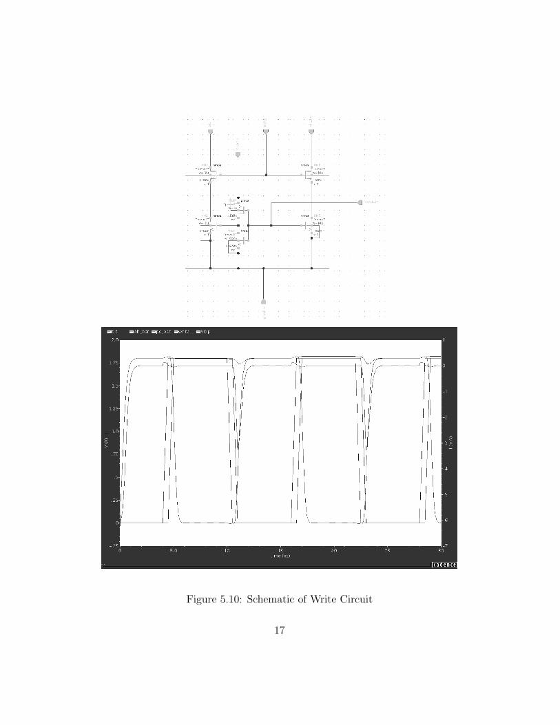
Figure 5.10: Schematic of Write Circuit
17

Figure 5.11: Layout of Write circuit
Figure 5.12: Schematic of Column Decoder
18

Figure 5.13: Layout of Column Decoder
19

Figure 5.14: Simulation of extracted netlist of Column Decoder
20

Figure 5.15: Schematic of 3:8 deoderdecoderayout of 7:128 decoder
21

Figure 5.16: Simulation of extracted netlist of 7:128 decoder
22

Chapter 6
2KB SRAM Memory
The complete layout of the Memory is shown in figure 7. In this diagramthe individual blocks described above are shown in the memory layout. Thememory occupies 598µm × 745µm which is less than 1mm2.The simulationof the whole schematic takes around 3700 seconds(little more than an hour)since the number of nets is around 38,000.
23

Chapter 7
Conclusion
In conclusion a 2KB SRAM was designed with 180nm technology to oper-ate at 50MHz. Each of the individual modules in the memory was layedlaidnd extracted for parasitics and simulated to meet the specifications.Theextracted netlist of the modules had parasitic capacitances not more that0.1fF.
24

Figure 7.1: Layout of 2KB SRAM
25

Bibliography
[1] Ken Kundert ”Principles of Top-Down Mixed-Signal Design” DesignersGuide Consulting, Inc.
[2] CY7C1049CV33 512K × 8 Static RAM, Cypress Semiconductor Corpo-ration
[3] Sourabh Khire, Gopikrishna Srinivasan, and Narayanan Terizhandur”SRAM MEMORY SYSTEM DESIGN”
[4] http://www.cedcc.psu.edu/khanjan/vssram.htm
26