Embed Size (px)
Citation preview
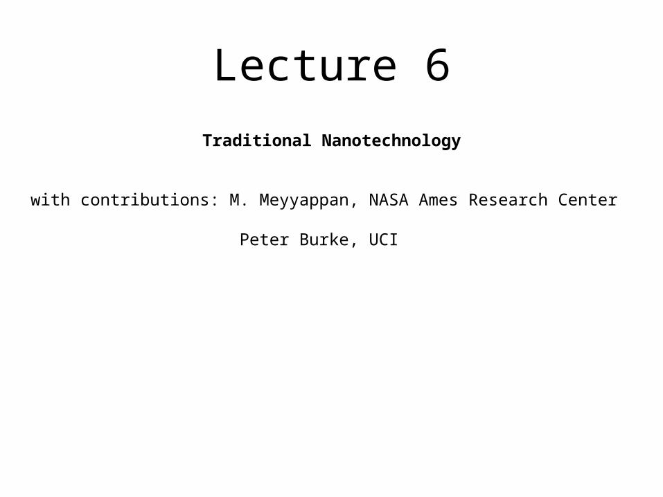
Traditional Nanotechnology
Lecture 6
with contributions: M. Meyyappan, NASA Ames Research Center
Peter Burke, UCI
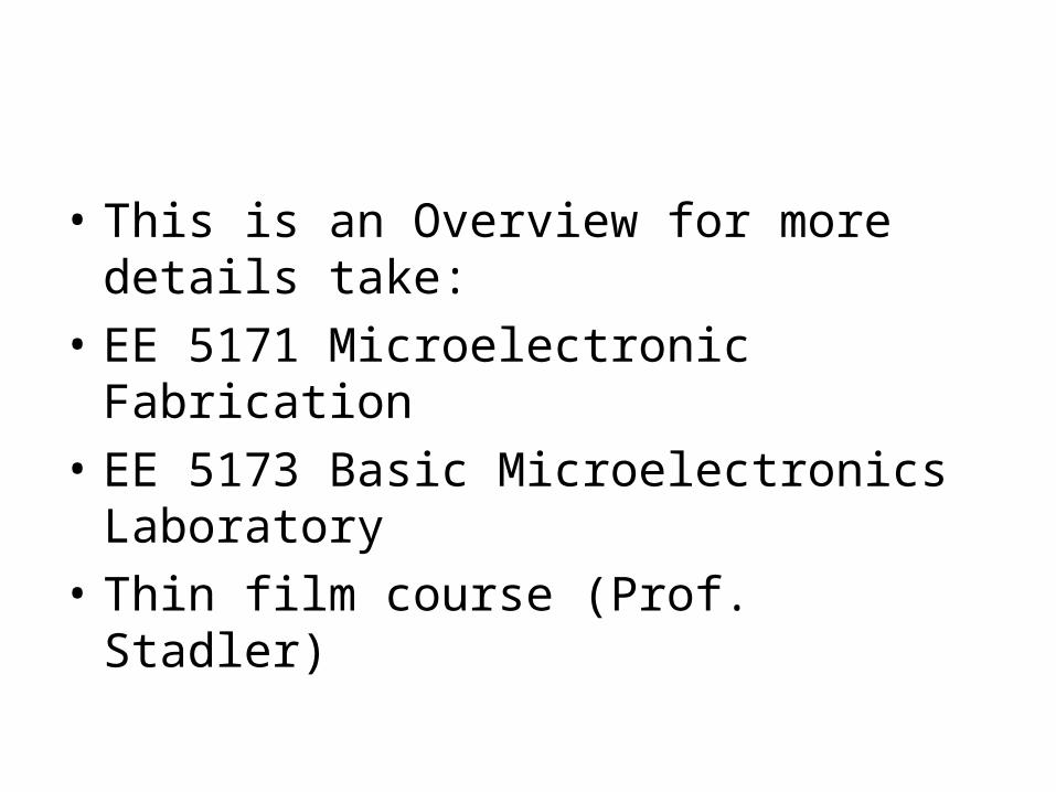
• This is an Overview for more details take:
• EE 5171 Microelectronic Fabrication
• EE 5173 Basic Microelectronics Laboratory
• Thin film course (Prof. Stadler)
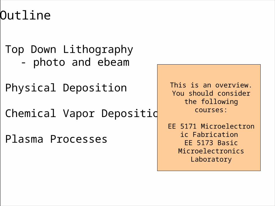
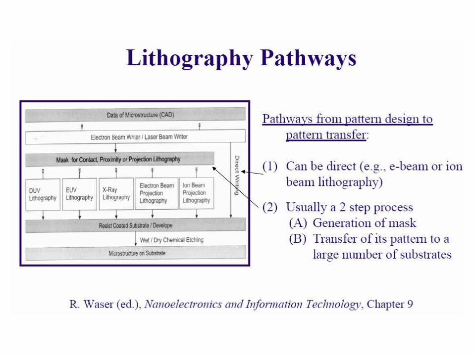
• Top Down Lithography - photo and ebeam
• Physical Deposition
• Chemical Vapor Deposition
• Plasma Processes
Outline
This is an overview. You should consider the following courses:
EE 5171 Microelectronic
Fabrication EE 5173 Basic
Microelectronics Laboratory

• Top Down Lithography - photo and ebeam
• Physical Deposition
• Chemical Vapor Deposition
• Plasma Processes
Outline
This is an overview. You should consider the following courses:
EE 5171 Microelectronic
Fabrication EE 5173 Basic
Microelectronics Laboratory
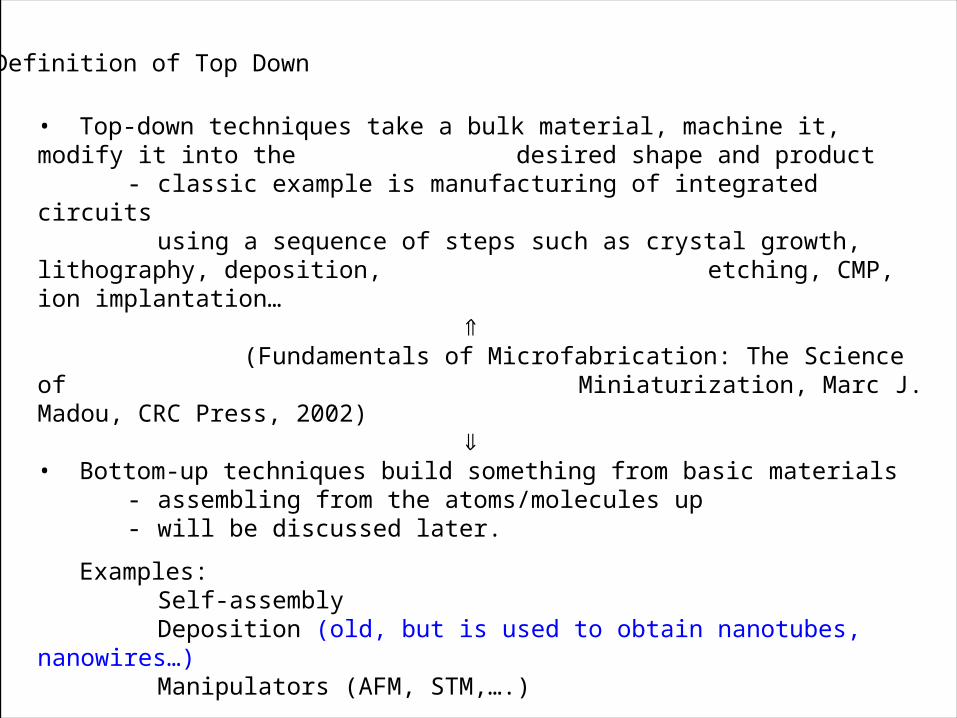
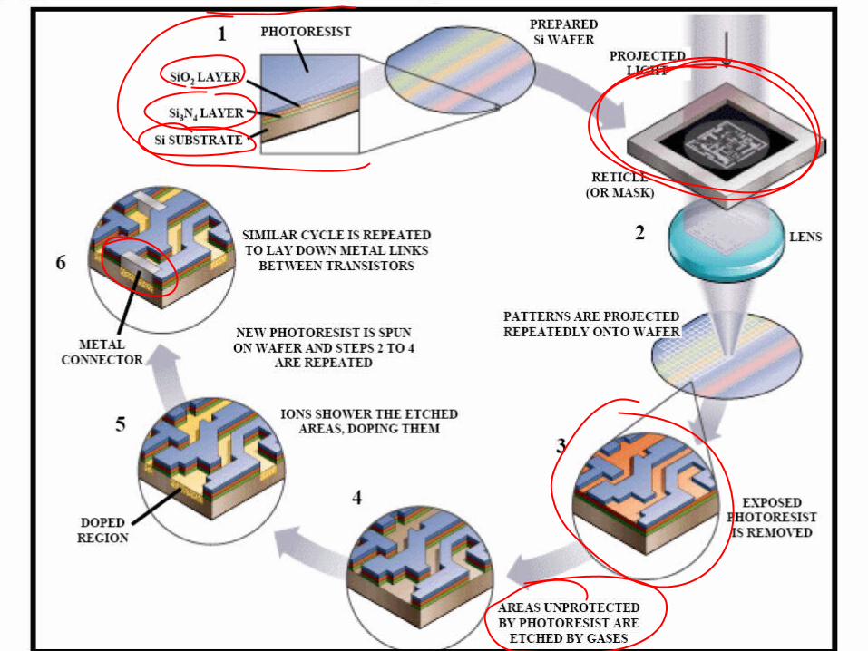
• Top-down techniques take a bulk material, machine it, modify it into the desired shape and product
- classic example is manufacturing of integrated circuits
using a sequence of steps such as crystal growth, lithography, deposition, etching, CMP, ion implantation…
(Fundamentals of Microfabrication: The Science
of Miniaturization, Marc J. Madou, CRC Press, 2002)
• Bottom-up techniques build something from basic materials
- assembling from the atoms/molecules up- will be discussed later.
Examples: Self-assemblyDeposition (old, but is used to obtain nanotubes,
nanowires…)Manipulators (AFM, STM,….)
Definition of Top Down
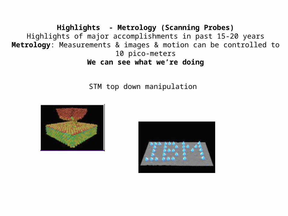
Highlights - Metrology (Scanning Probes)Highlights of major accomplishments in past 15-20 years
Metrology: Measurements & images & motion can be controlled to 10 pico-metersWe can see what we’re doing
STM top down manipulation
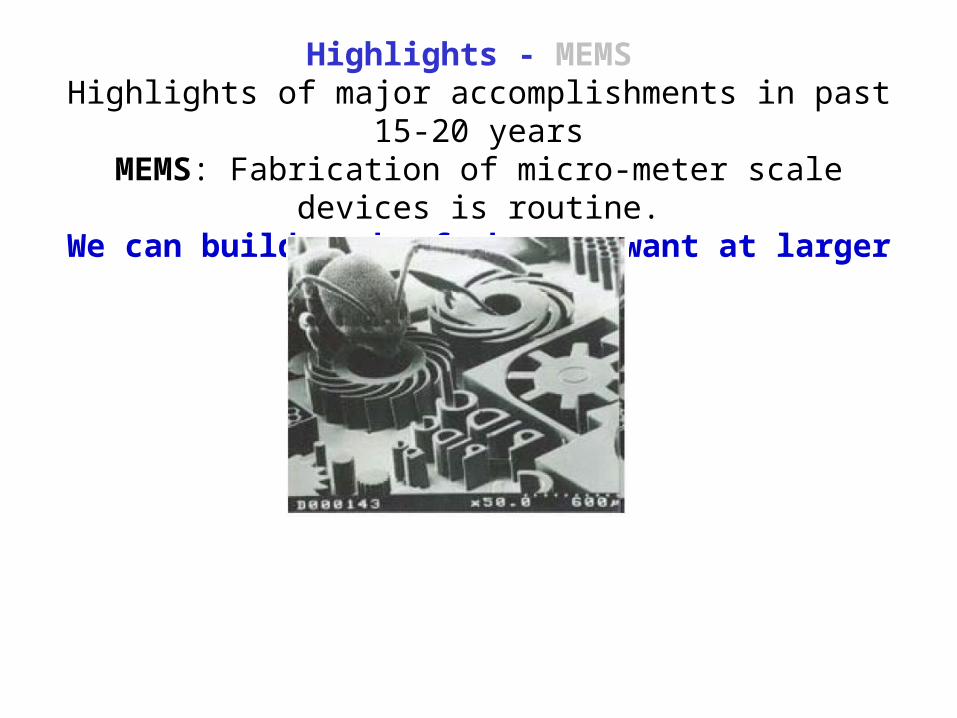
Highlights - MEMS Highlights of major accomplishments in past 15-20 years
MEMS: Fabrication of micro-meter scale devices is routine.We can build much of what we want at larger scales.
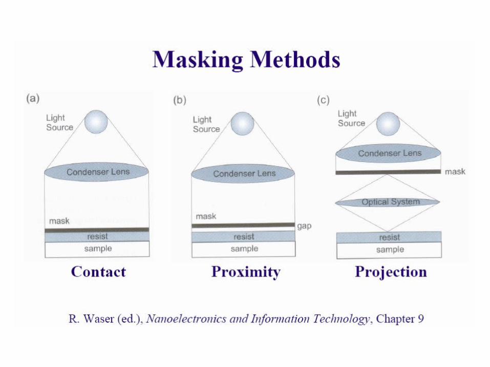
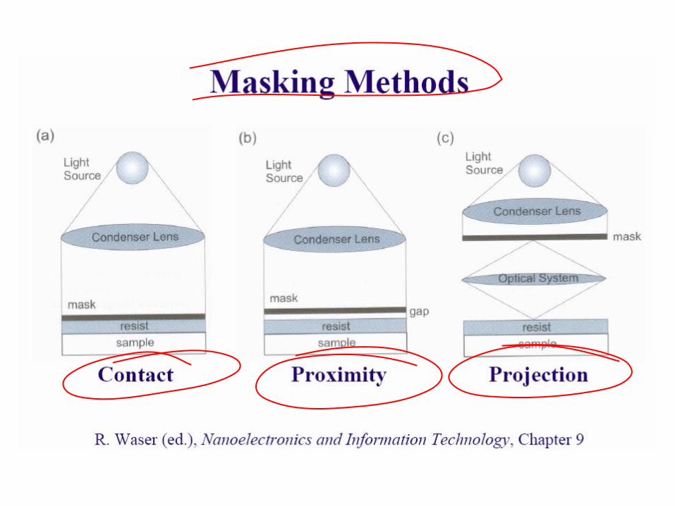
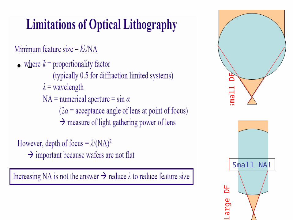
• -
smal
l DF
Small NA!
Larg
e D
F
smal
l DF
Small NA!
Larg
e D
epth
of
Foc
us
Small NA!
Larg
e D
F
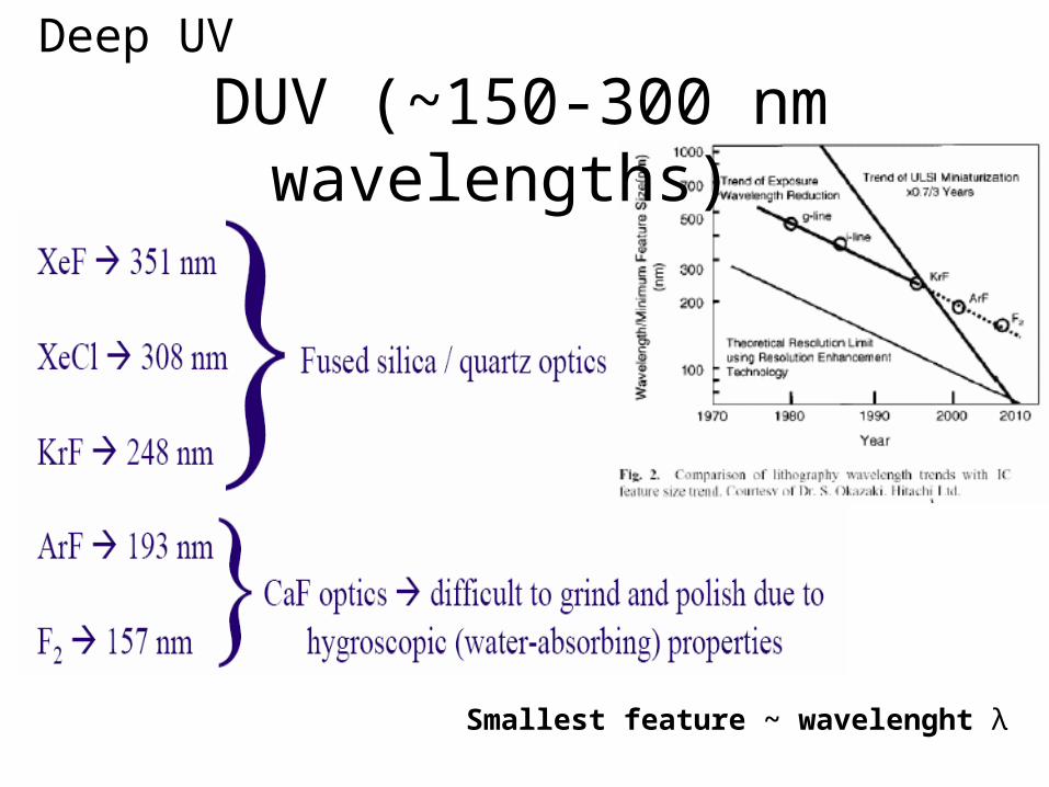
Smallest feature ~ wavelenght λ
DUV (~150-300 nm wavelengths) Deep UV
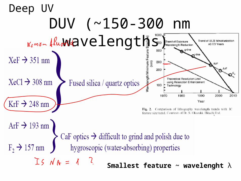
Smallest feature ~ wavelenght λ
DUV (~150-300 nm wavelengths) Deep UV
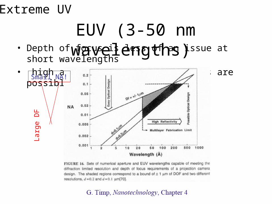
EUV (3-50 nm wavelengths) • Depth of focus is less of an issue at short wavelengths• high aspect ratio resist profiles are possible with EUV
Extreme UV
Small NA!
Larg
e D
F
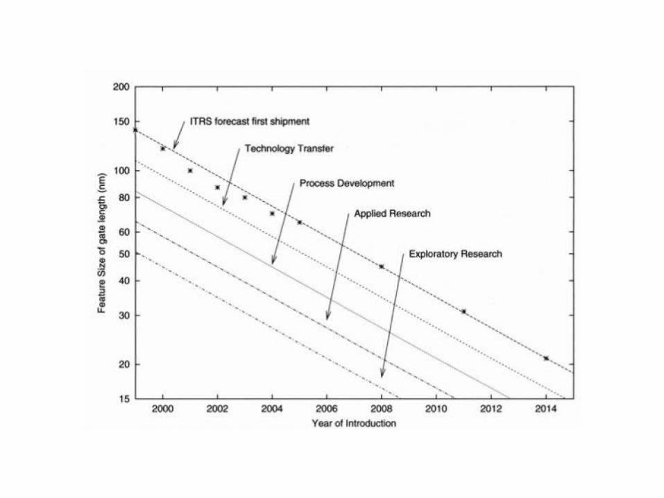
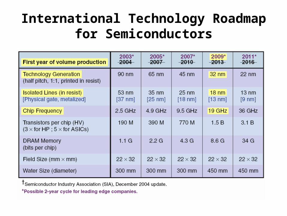
International Technology Roadmapfor Semiconductors
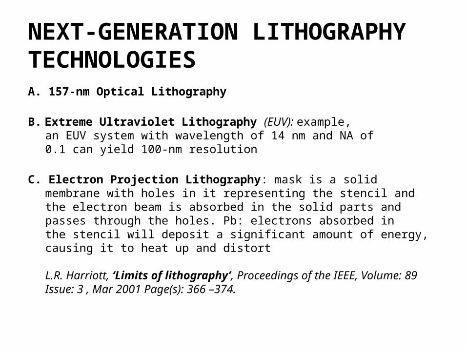
NEXT-GENERATION LITHOGRAPHYTECHNOLOGIESA. 157-nm Optical Lithography
B. Extreme Ultraviolet Lithography (EUV): example,an EUV system with wavelength of 14 nm and NA of0.1 can yield 100-nm resolution
C. Electron Projection Lithography: mask is a solidmembrane with holes in it representing the stencil andthe electron beam is absorbed in the solid parts andpasses through the holes. Pb: electrons absorbed inthe stencil will deposit a significant amount of energy,causing it to heat up and distort
L.R. Harriott, ‘Limits of lithography’, Proceedings of the IEEE, Volume: 89 Issue: 3 , Mar 2001 Page(s): 366 –374.
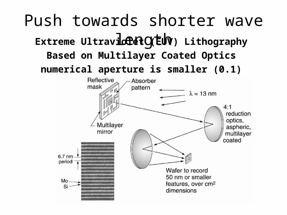
Push towards shorter wave lengthExtreme Ultraviolet (EUV) Lithography
Based on Multilayer Coated Optics
numerical aperture is smaller (0.1)
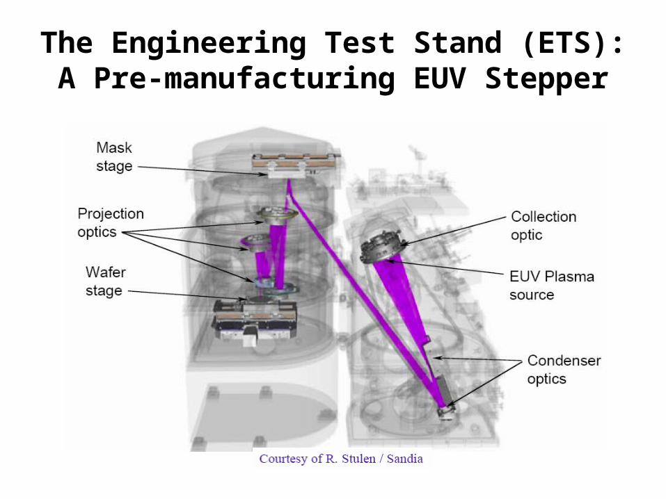
The Engineering Test Stand (ETS):A Pre-manufacturing EUV Stepper
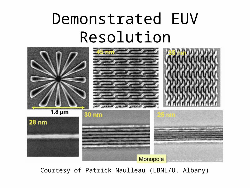
Demonstrated EUV Resolution
Courtesy of Patrick Naulleau (LBNL/U. Albany)
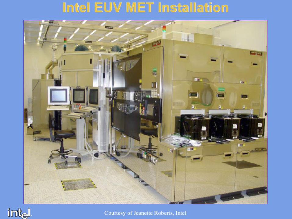
costs
very high cost (Intel and others team up to afford a fab)
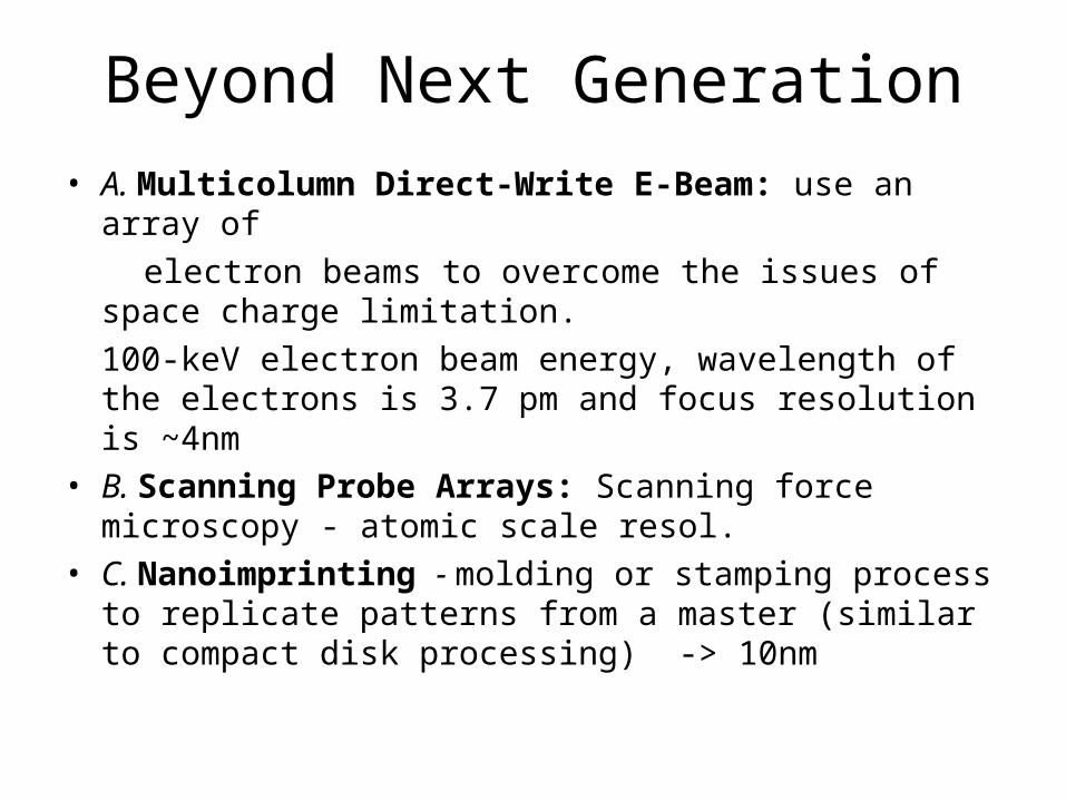
Beyond Next Generation
• A. Multicolumn Direct-Write E-Beam: use an array of
electron beams to overcome the issues of space charge limitation.
100-keV electron beam energy, wavelength of the electrons is 3.7 pm and focus resolution is ~4nm
• B. Scanning Probe Arrays: Scanning force microscopy - atomic scale resol.
• C. Nanoimprinting - molding or stamping process to replicate patterns from a master (similar to compact disk processing) -> 10nm
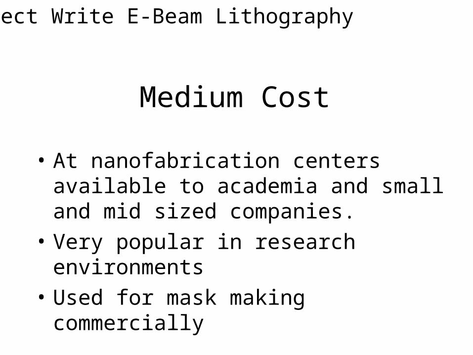
Medium Cost
• At nanofabrication centers available to academia and small and mid sized companies.
• Very popular in research environments
• Used for mask making commercially
Direct Write E-Beam Lithography
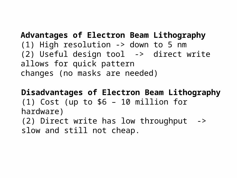
Advantages of Electron Beam Lithography(1) High resolution -> down to 5 nm(2) Useful design tool -> direct write allows for quick patternchanges (no masks are needed)
Disadvantages of Electron Beam Lithography(1) Cost (up to $6 – 10 million for hardware)(2) Direct write has low throughput -> slow and still not cheap.

SEM converted to do Lithography
• Scanning Electron Beam Lithography
Exposure source: electron beam
At acceleration voltage Vc=120kV, λ=0.0336Å
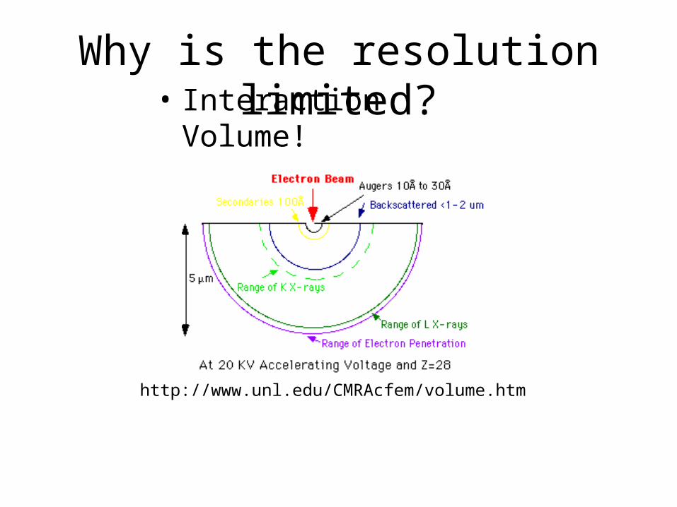
Why is the resolution limited?• Interaction Volume!
http://www.unl.edu/CMRAcfem/volume.htm
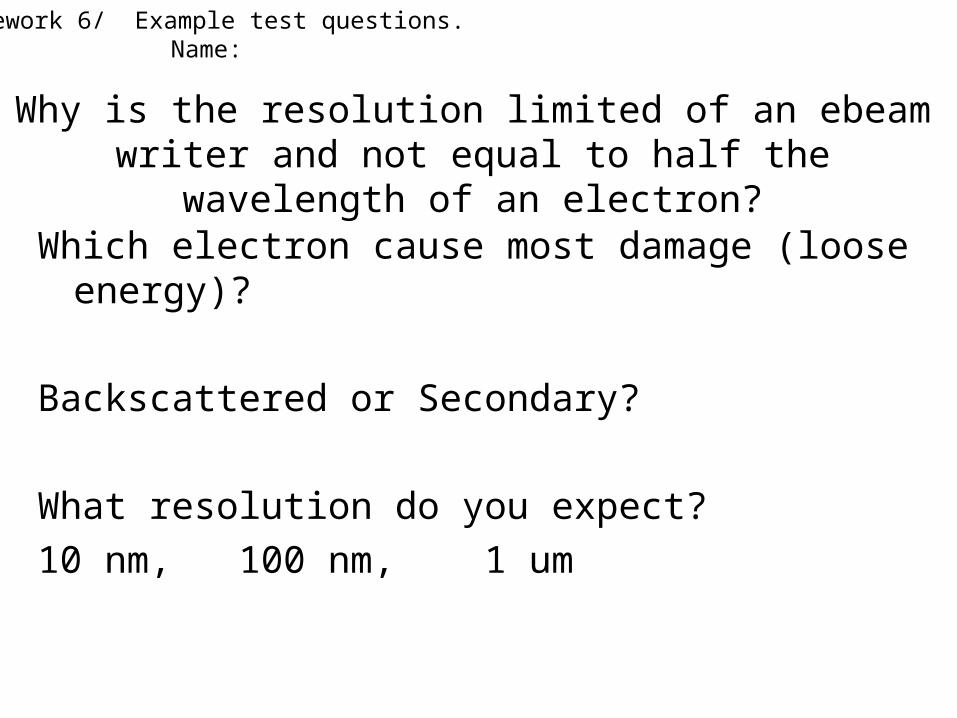
Which electron cause most damage (loose energy)?
Backscattered or Secondary?
What resolution do you expect?
10 nm, 100 nm, 1 um
Why is the resolution limited of an ebeam writer and not equal to half the wavelength of an electron?
Homework 6/ Example test questions.Name:
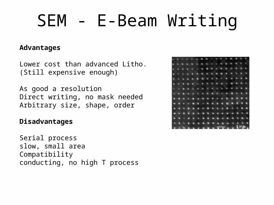
SEM - E-Beam Writing
Advantages
Lower cost than advanced Litho. (Still expensive enough)
As good a resolutionDirect writing, no mask neededArbitrary size, shape, order
Disadvantages
Serial processslow, small areaCompatibilityconducting, no high T process
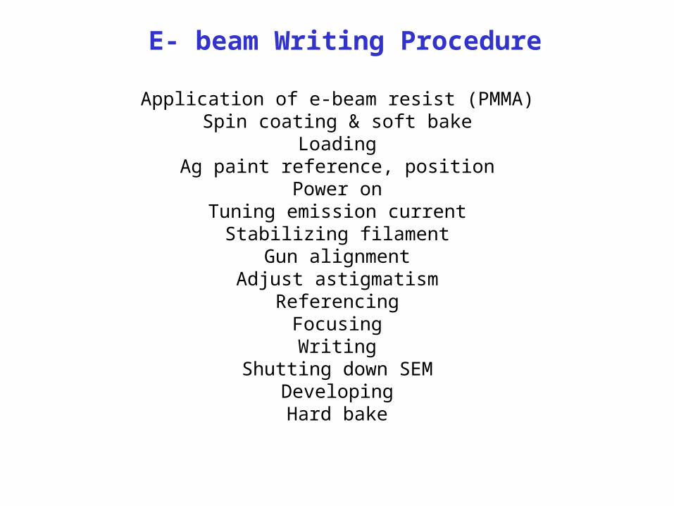
E- beam Writing Procedure
Application of e-beam resist (PMMA)Spin coating & soft bake
LoadingAg paint reference, position
Power onTuning emission current
Stabilizing filamentGun alignment
Adjust astigmatismReferencing
FocusingWriting
Shutting down SEMDevelopingHard bake
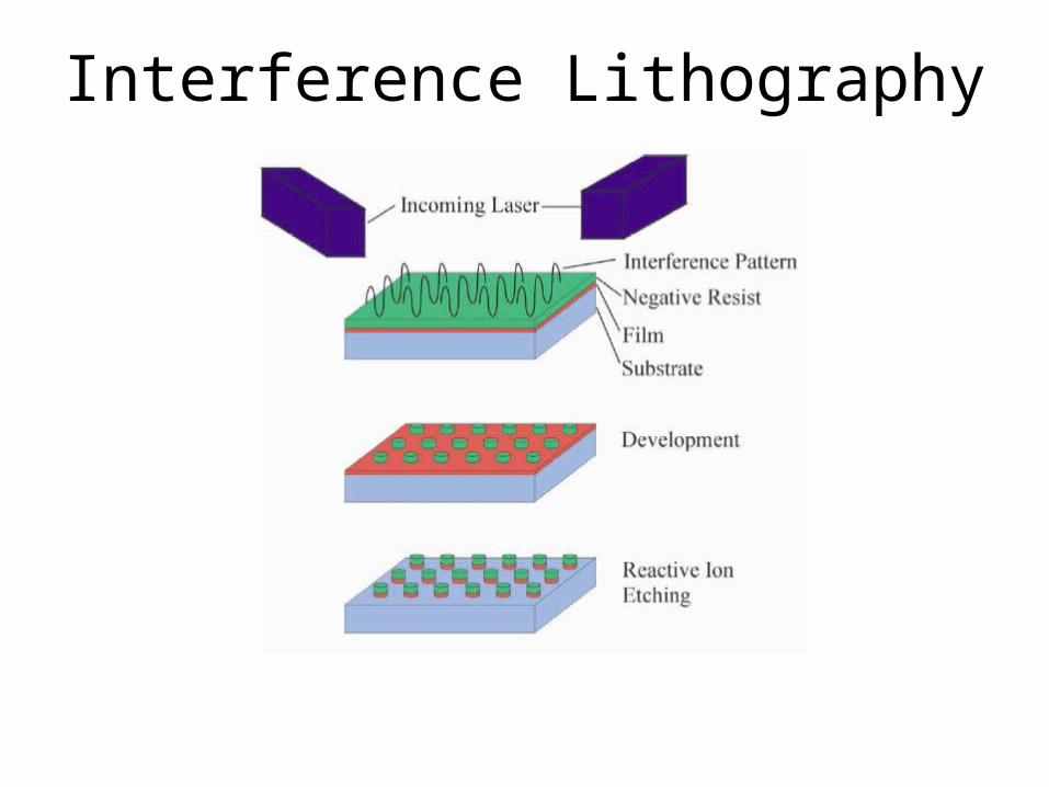
Interference Lithography
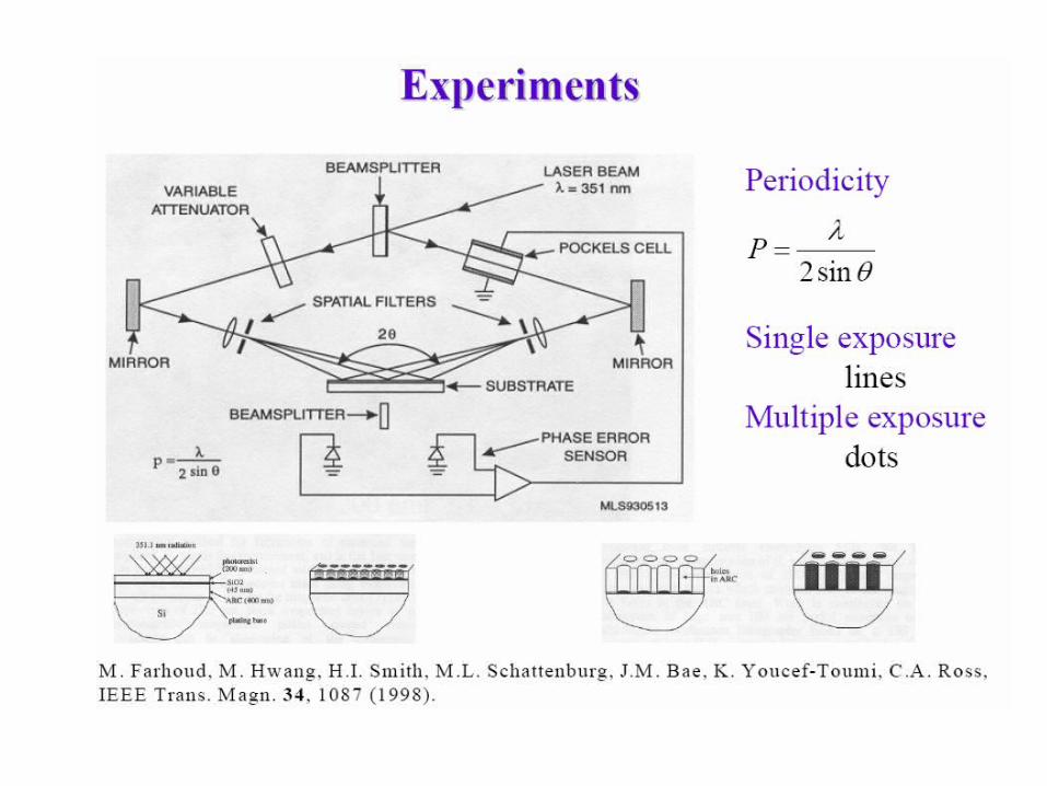
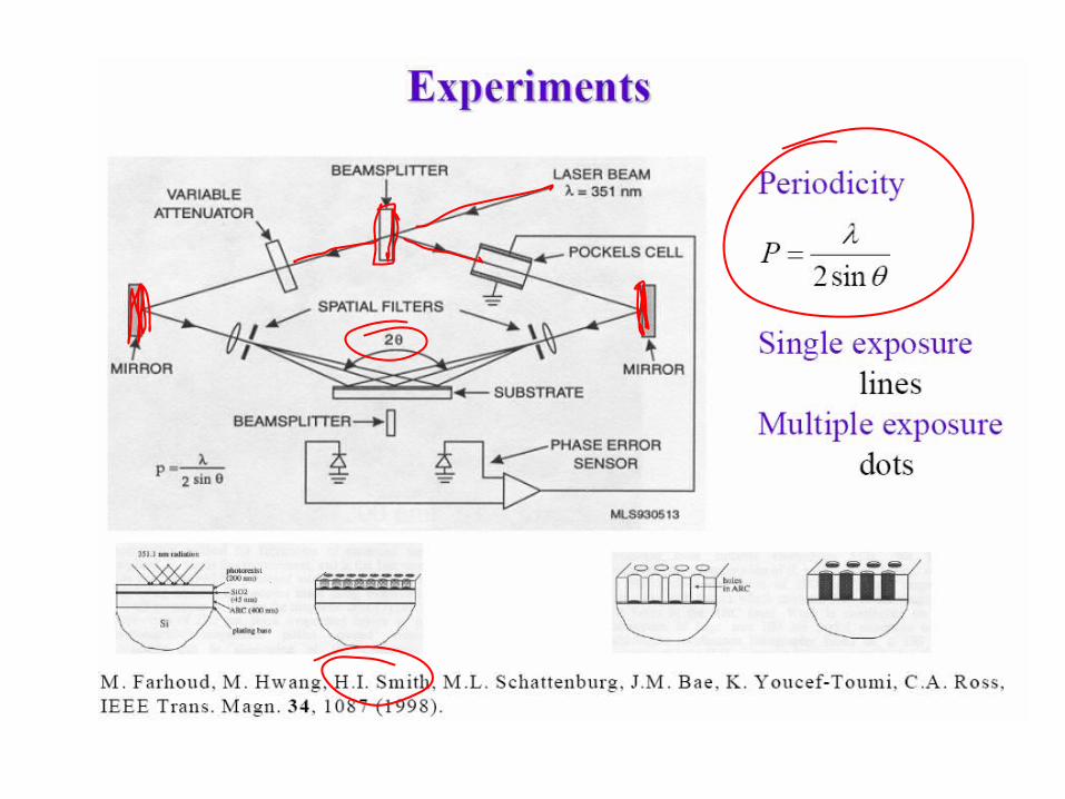
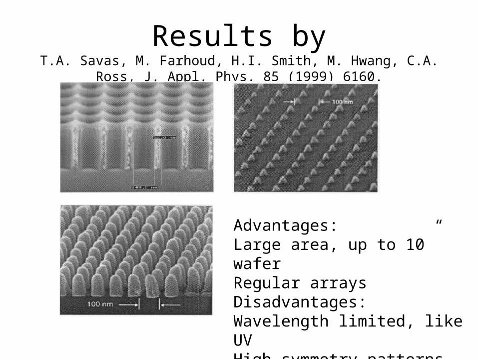
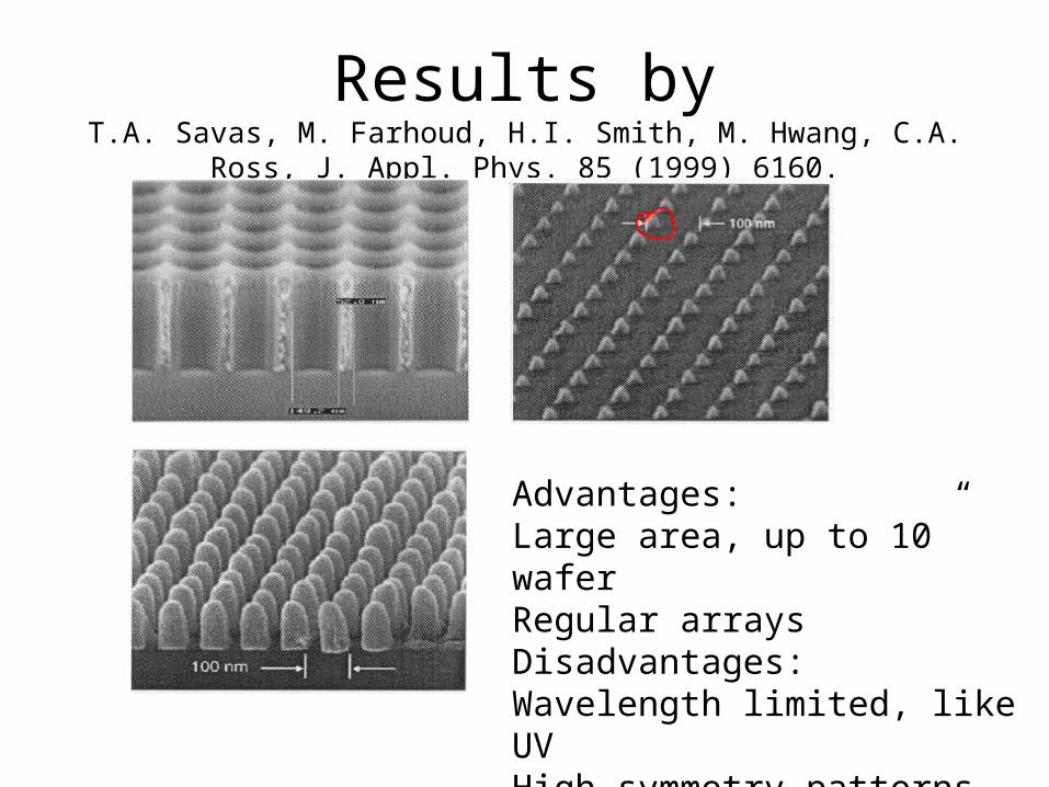
Results byT.A. Savas, M. Farhoud, H.I. Smith, M. Hwang, C.A. Ross, J. Appl.
Phys. 85 (1999) 6160.
Advantages:Large area, up to 10” waferRegular arraysDisadvantages:Wavelength limited, like UVHigh symmetry patterns
Results byT.A. Savas, M. Farhoud, H.I. Smith, M. Hwang, C.A. Ross, J. Appl.
Phys. 85 (1999) 6160.
Advantages:Large area, up to 10” waferRegular arraysDisadvantages:Wavelength limited, like UVHigh symmetry patterns
Homework 6/ Example test questions.Name:
• Name three top down Micro/Nanofabrication methods?
• Write down what limits the resolution in each cases?
• Write down the minimal line width that you expect?
• Classify the throughput using parallel (fast) and serial (slow)?
• Which once are available to small companies?
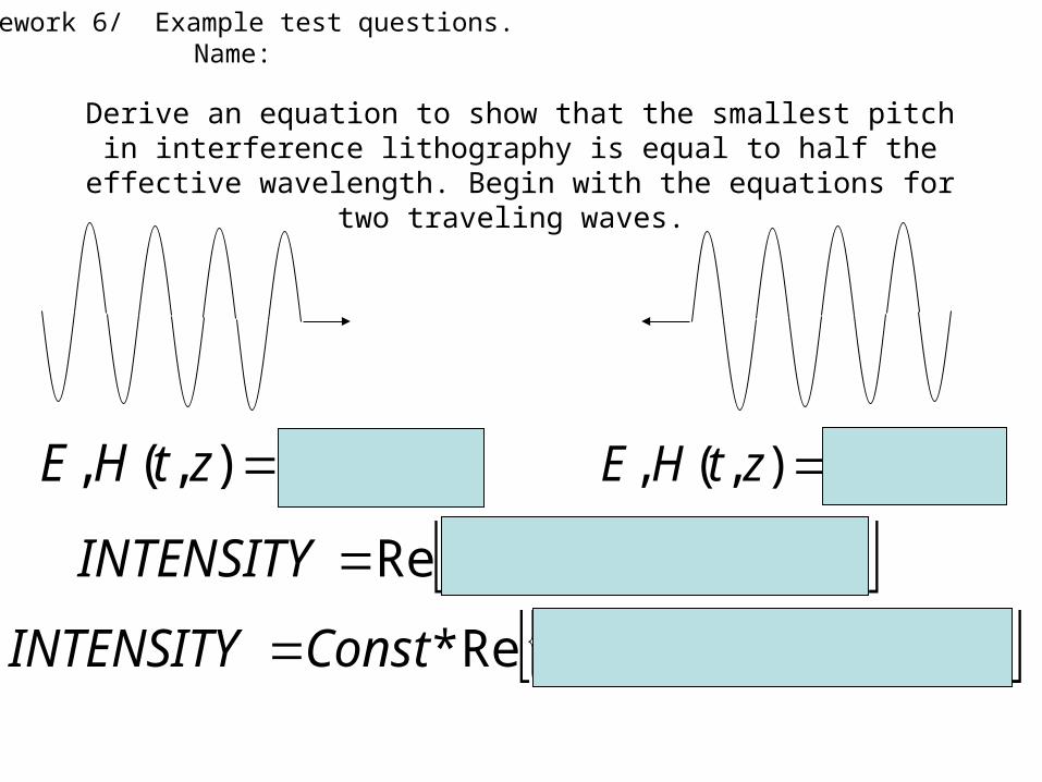
Derive an equation to show that the smallest pitch in interference lithography is equal to half the effective wavelength. Begin with the
equations for two traveling waves.
tjjkzeAeztHE ),(, tjjkzeAeztHE ),(,
22 )()(Re tjjkzjkz AeeeINTENSITY
tjkzjkzj eeeConstINTENSITY 222 )(21Re*
Homework 6/ Example test questions.Name:
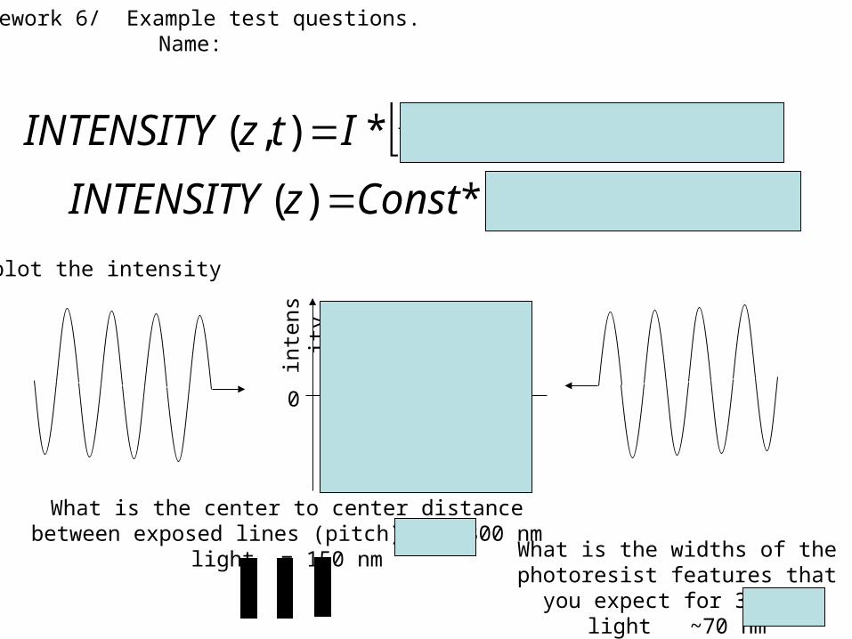
inte
nsity
0
)2cos()2cos(1*),( tkzItzINTENSITY
plot the intensity
)2cos(1*)( kzConstzINTENSITY
What is the center to center distance between exposed lines (pitch) for 300 nm light = 150 nm
What is the widths of the photoresist features that you
expect for 300 nm light ~70 nm
Homework 6/ Example test questions.Name:
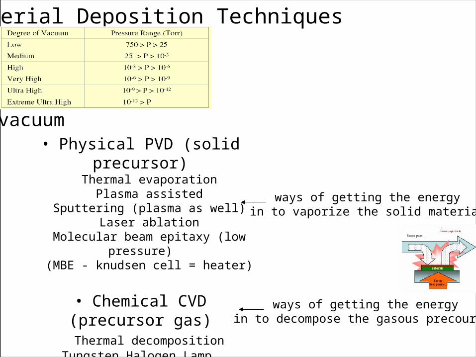
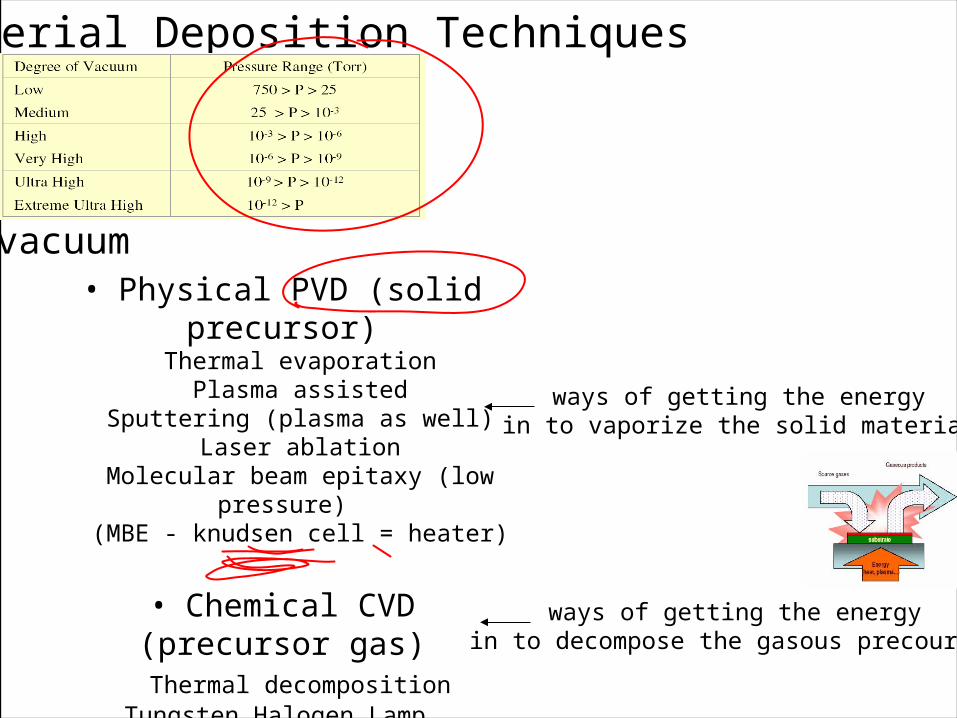
Material Deposition Techniques
• Physical PVD (solid precursor)Thermal evaporation
Plasma assistedSputtering (plasma as well)
Laser ablationMolecular beam epitaxy (low pressure)
(MBE - knudsen cell = heater)
• Chemical CVD (precursor gas)Thermal decomposition
Tungsten Halogen Lamp Plasma assisted
MBE (low pressure)
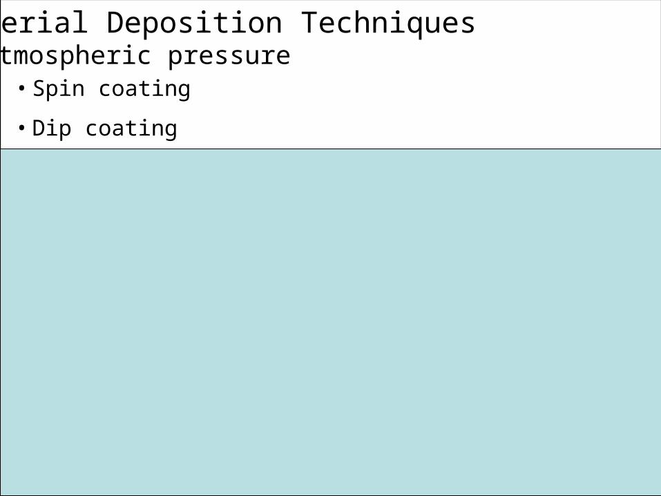
• Spin coating
• Dip coating
Material Deposition Techniques
vacuum (consider thin film class)
atmospheric pressure
ways of getting the energy in to vaporize the solid material
ways of getting the energy in to decompose the gasous precourser
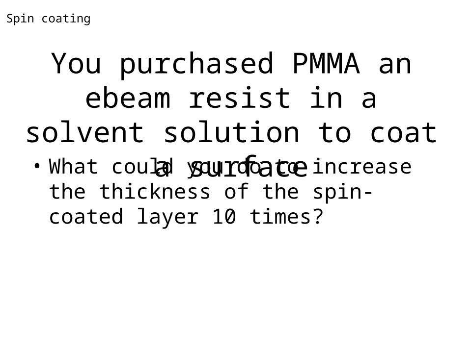
You purchased PMMA an ebeam resist in a solvent solution to coat a surface
• What could you do to increase the thickness of the spin-coated layer 10 times?
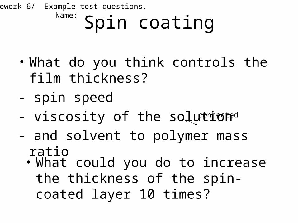
Spin coating
Spin coating
• What do you think controls the film thickness?
- spin speed
- viscosity of the solution
- and solvent to polymer mass ratio
connected
• What could you do to increase the thickness of the spin-coated layer 10 times?
Homework 6/ Example test questions.Name:
Gas phase processes
Material Deposition Techniques
• Physical PVD (solid precursor)Thermal evaporation
Plasma assistedSputtering (plasma as well)
Laser ablationMolecular beam epitaxy (low pressure)
(MBE - knudsen cell = heater)
• Chemical CVD (precursor gas)Thermal decomposition
Tungsten Halogen Lamp Plasma assisted
MBE (low pressure)
• Spin coating
• Dip coating
Material Deposition Techniques
vacuum
atmospheric pressure
ways of getting the energy in to vaporize the solid material
ways of getting the energy in to decompose the gasous precourser
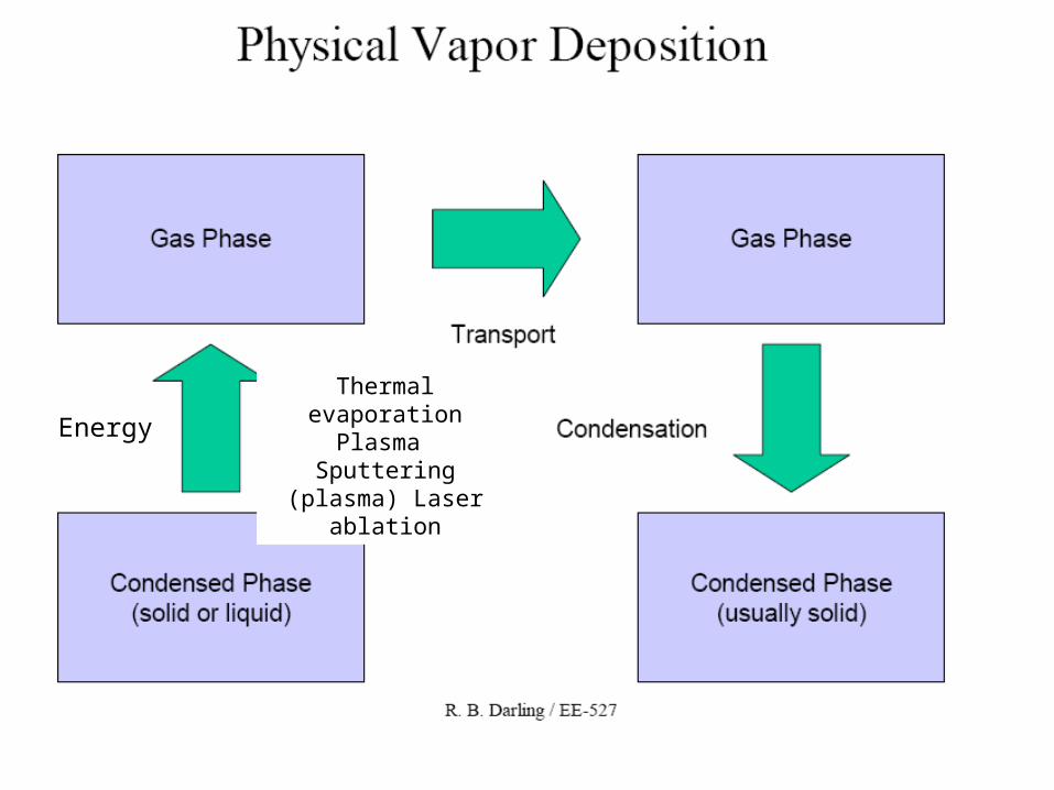
CVD and PVD deposition processes to deposit crystalline and non-crystalline films
Thermal evaporationPlasma
Sputtering (plasma) Laser ablation
Energy
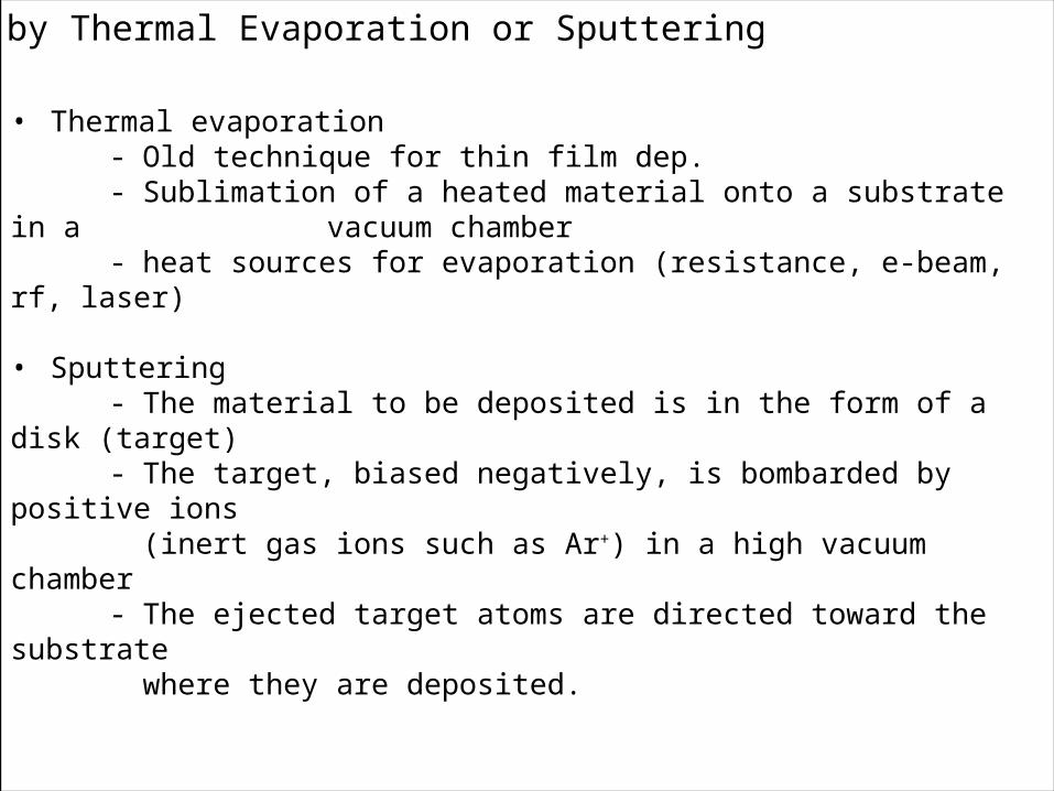
• Thermal evaporation- Old technique for thin film dep.- Sublimation of a heated material onto a substrate in a vacuum chamber- heat sources for evaporation (resistance, e-beam, rf, laser)
• Sputtering- The material to be deposited is in the form of a disk (target)- The target, biased negatively, is bombarded by positive ions
(inert gas ions such as Ar+) in a high vacuum chamber- The ejected target atoms are directed toward the substrate
where they are deposited.
PVD by Thermal Evaporation or Sputtering
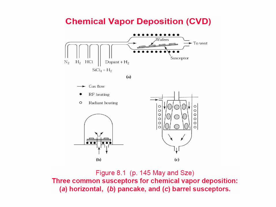
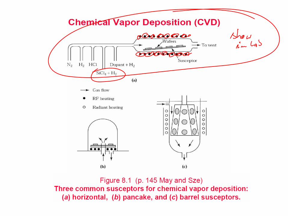
• Uses chemical precursors to deposit thin films or other nanostructures (carbon nanotubes, nanowires) on a substrate
• Energy to break the precursors into reactive radicals is supplied by heating
- Heating substrate only (by rf, inductive, resistive heaters) is accomplished in cold wall reactors- Hot wall reactor (such as a tube inside a furnace)
• Sequence of Key Steps(1) Diffusion of reactants to the substrate(2) Adsorption onto the surface(3) Surface chemical reaction(s) leading to deposition of solid(4) Gaseous byproducts desorption from the surface(5) Gaseous byproducts diffusing into the stream
Chemical Vapor Deposition
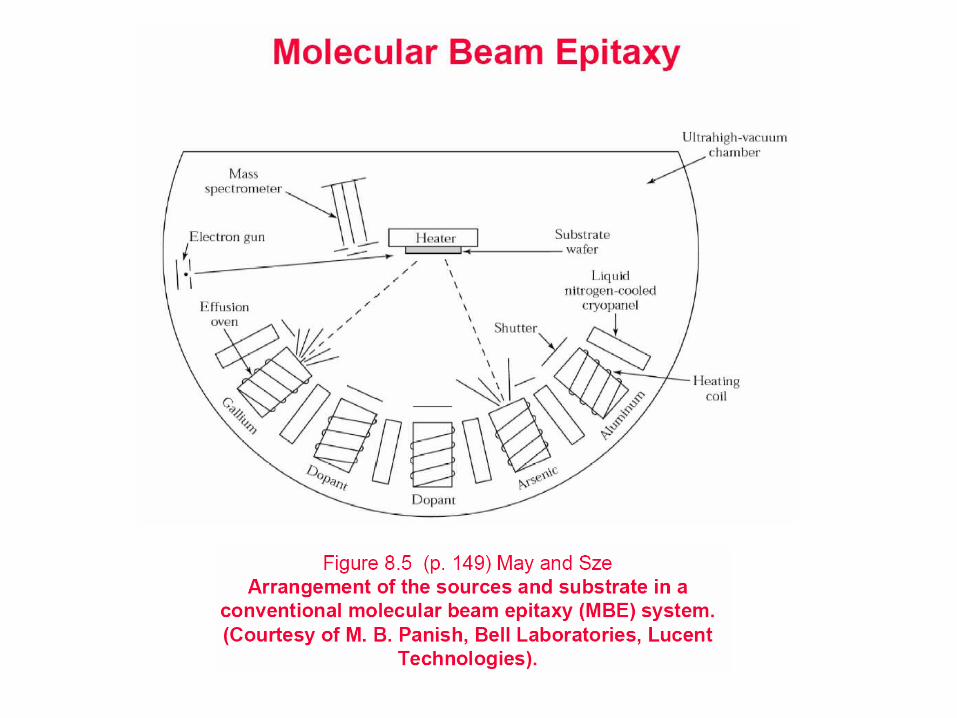
MBE (used to grow crystals and thin films with sub 1 nm control)
• Low-Temperature
• evaporation at very low deposition rates
• typically in ultra-high vacuum
• very well controlled
• grow films with good crystal structure
• expensive
• often use multiple sources to grow alloy films
• Knowledge section:
As usual we try to look at some relationships to enhance our knowledge
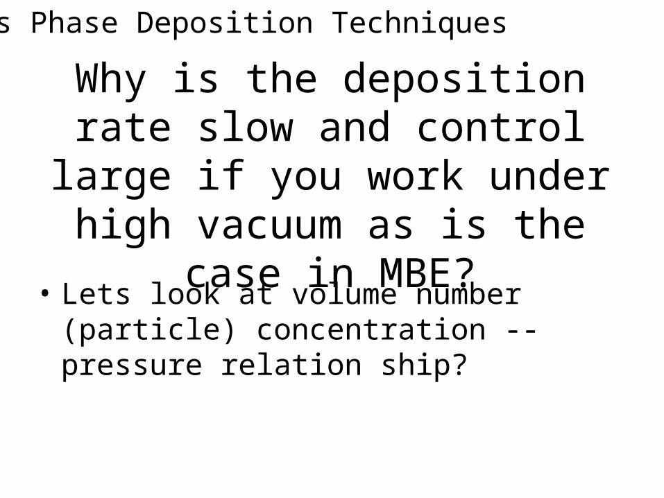
Why is the deposition rate slow and control large if you work under high vacuum as is the
case in MBE?
• Lets look at volume number (particle) concentration -- pressure relation ship?
Gas Phase Deposition Techniques
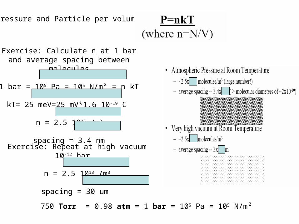
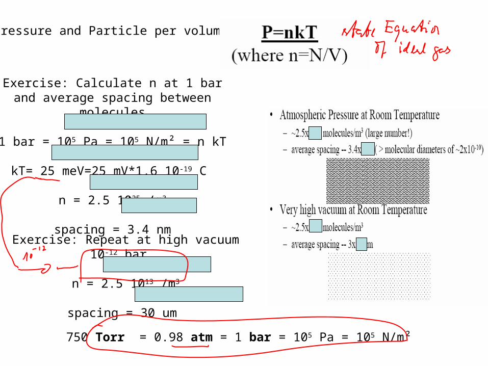
Exercise: Calculate n at 1 bar and average spacing between molecules
1 bar = 105 Pa = 105 N/m² = n kT
kT= 25 meV=25 mV*1.6 10-19 C
n = 2.5 1025 /m3
spacing = 3.4 nm
750 Torr = 0.98 atm = 1 bar = 105 Pa = 105 N/m²
Pressure and Particle per volume
Exercise: Repeat at high vacuum 10-12 bar
n = 2.5 1013 /m3
spacing = 30 um
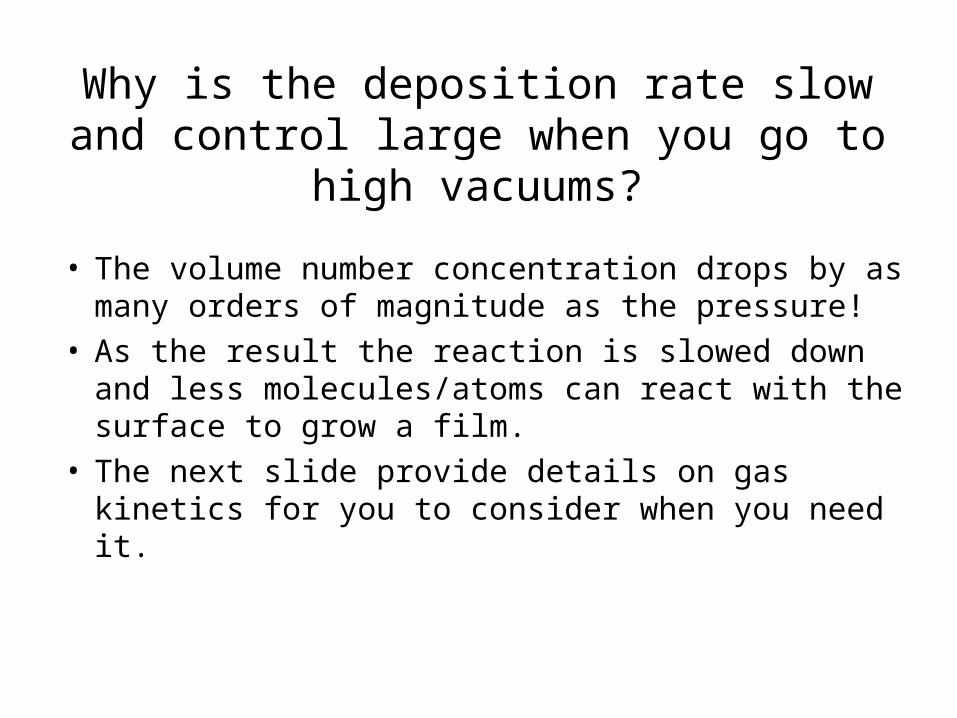
Why is the deposition rate slow and control large when you go to high vacuums?
• The volume number concentration drops by as many orders of magnitude as the pressure!
• As the result the reaction is slowed down and less molecules/atoms can react with the surface to grow a film.
• The next slide provide details on gas kinetics for you to consider when you need it.
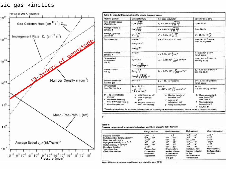
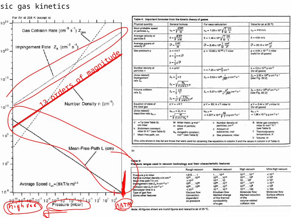
Basic gas kinetics
13 orders of m
agnitude
Basic gas kinetics
13 orders of m
agnitude
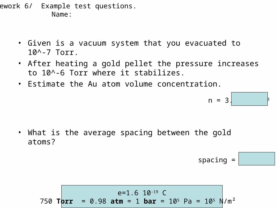
e=1.6 10-19 C750 Torr = 0.98 atm = 1 bar = 105 Pa = 105 N/m²
• Given is a vacuum system that you evacuated to 10^-7 Torr. • After heating a gold pellet the pressure increases to 10^-6 Torr
where it stabilizes.• Estimate the Au atom volume concentration.
• What is the average spacing between the gold atoms?
n = 3.3 1016 /m3
spacing = 3.1 um
Homework 6/ Example test questions.Name:

• Physical PVD (solid precursor)Thermal evaporation
Plasma assistedSputtering (plasma as well)
Laser ablationMolecular beam epitaxy (low pressure)
(MBE - knudsen cell = heater)
• Chemical CVD (precursor gas)Thermal decomposition
Tungsten Halogen Lamp Plasma assisted
MBE (low pressure)
• Spin coating
• Dip coating
Material Deposition Techniques
vacuum
atmospheric pressure
ways of getting the energy in to vaporize the solid material
ways of getting the energy in to decompose the gasous precourser
• How does this relate to Nanotechnology?
-- Traditional Nano
-- Nanomaterials
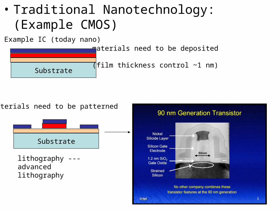
• Traditional Nanotechnology: (Example CMOS)
Substrate
Example IC (today nano)materials need to be deposited
(film thickness control ~1 nm)
Materials need to be patterned
Substrate
lithography --- advanced lithography
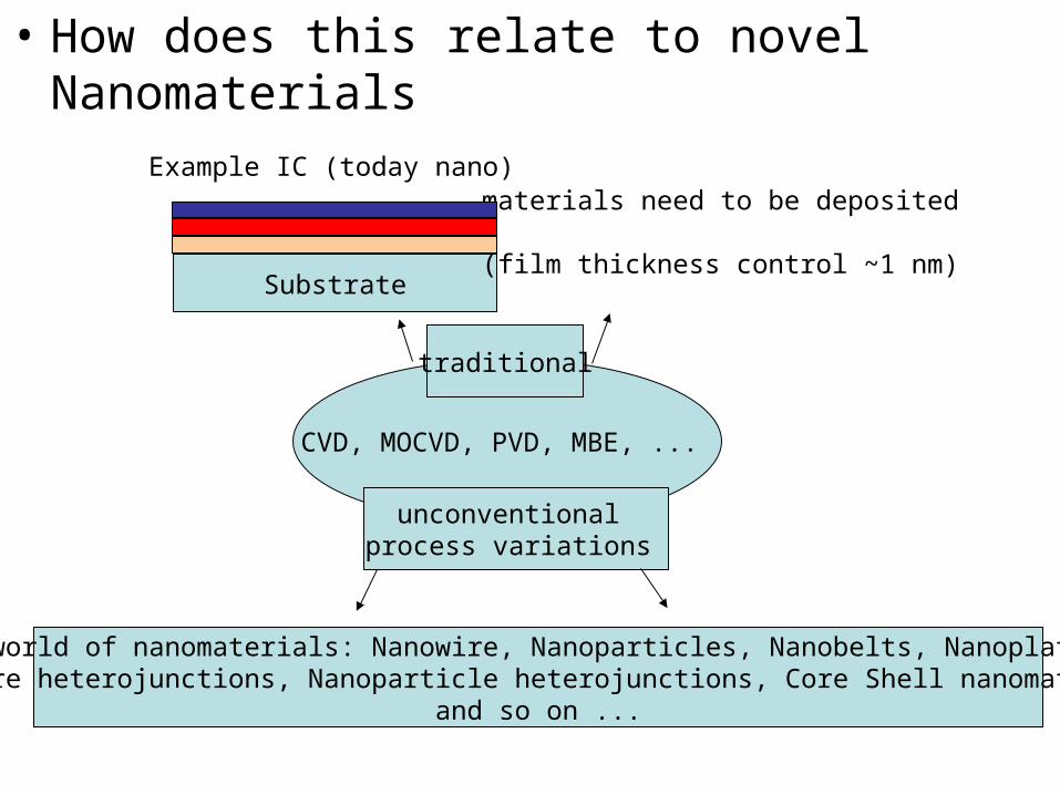
• How does this relate to novel Nanomaterials
Substrate
Example IC (today nano)materials need to be deposited
(film thickness control ~1 nm)
CVD, MOCVD, PVD, MBE, ...
unconventional process variations
traditional
The world of nanomaterials: Nanowire, Nanoparticles, Nanobelts, NanoplateletsNanowire heterojunctions, Nanoparticle heterojunctions, Core Shell nanomaterials
and so on ...
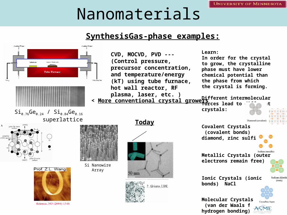
Nanomaterials
2 m
Si Nanowire Array
Si0.76Ge0.24 / Si0.84Ge0.16 superlattice
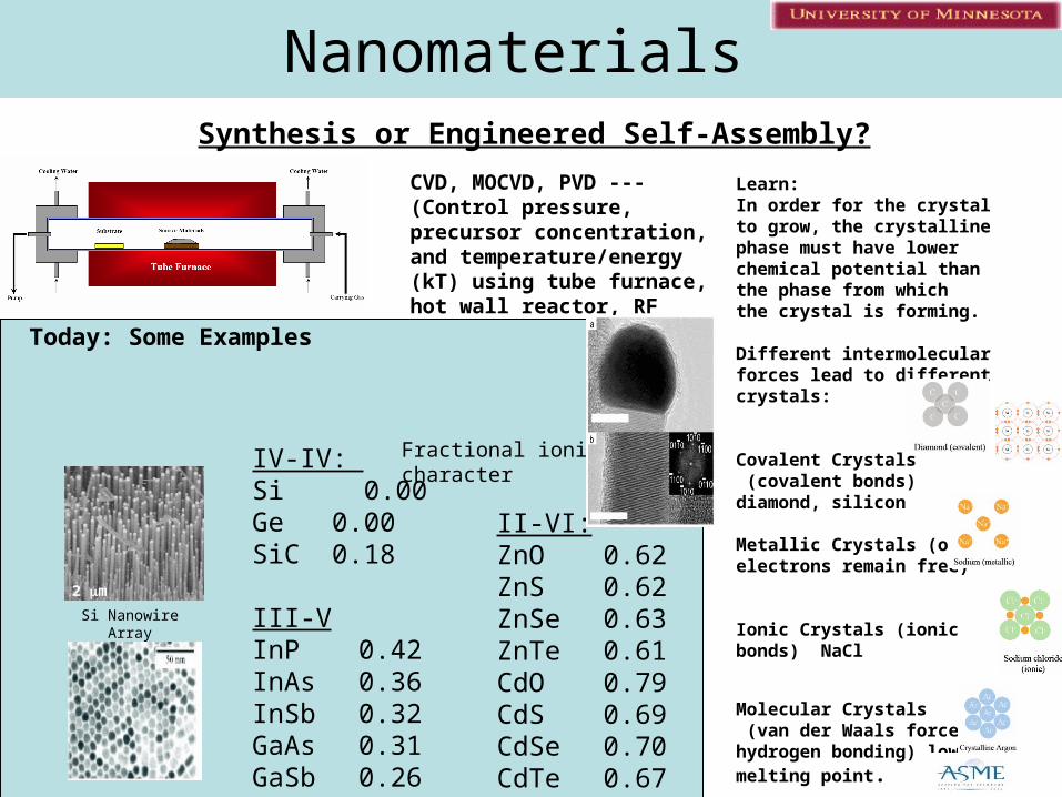
CVD, MOCVD, PVD --- (Control pressure, precursor concentration, and temperature/energy (kT) using tube furnace, hot wall reactor, RF plasma, laser, etc. )
< More conventional crystal growers
Learn: In order for the crystal to grow, the crystalline phase must have lower chemical potential than the phase from which the crystal is forming.
Different intermolecular forces lead to different crystals:
Covalent Crystals (covalent bonds) diamond, zinc sulfide
Metallic Crystals (outer electrons remain free)
Ionic Crystals (ionic bonds) NaCl
Molecular Crystals (van der Waals force or hydrogen bonding) lower melting point.
SynthesisGas-phase examples:
Today
Nanomaterials
CVD, MOCVD, PVD --- (Control pressure, precursor concentration, and temperature/energy (kT) using tube furnace, hot wall reactor, RF plasma, laser, etc. )
Learn: In order for the crystal to grow, the crystalline phase must have lower chemical potential than the phase from which the crystal is forming.
Different intermolecular forces lead to different crystals:
Covalent Crystals (covalent bonds) diamond, silicon
Metallic Crystals (outer electrons remain free)
Ionic Crystals (ionic bonds) NaCl
Molecular Crystals (van der Waals force or hydrogen bonding) lower melting point.
Synthesis or Engineered Self-Assembly?
2 m
Si Nanowire Array
Today: Some Examples
IV-IV: Si 0.00 Ge 0.00SiC 0.18
III-VInP 0.42InAs 0.36InSb 0.32GaAs 0.31GaSb 0.26
Fractional ionic character
II-VI:ZnO 0.62ZnS 0.62ZnSe 0.63ZnTe 0.61CdO 0.79CdS 0.69CdSe 0.70CdTe 0.67
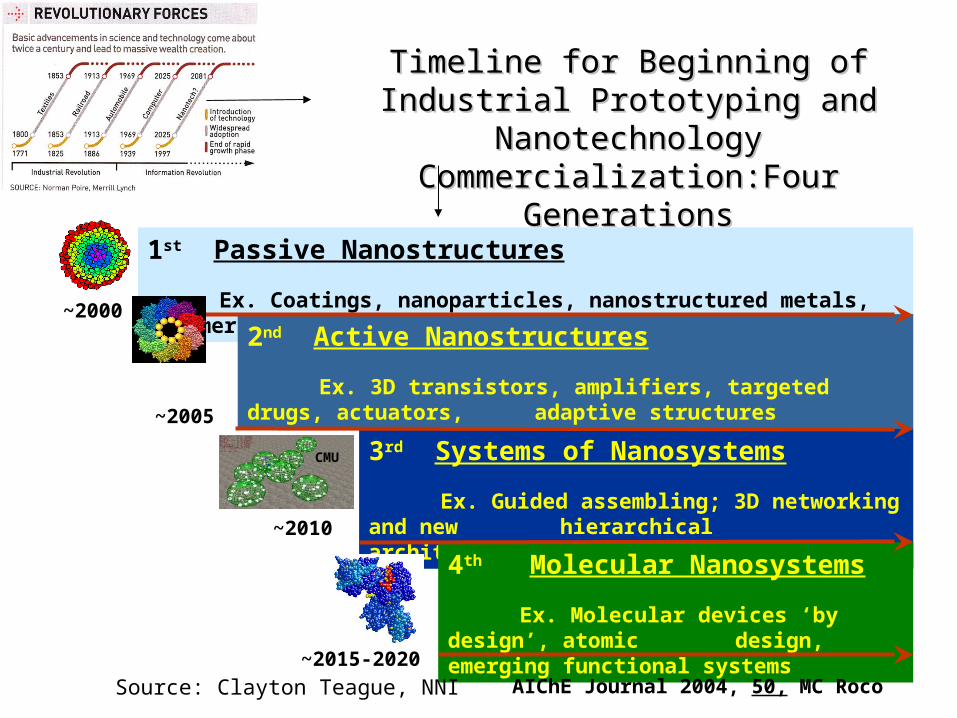
Timeline for Beginning of Industrial Timeline for Beginning of Industrial Prototyping and Nanotechnology Prototyping and Nanotechnology
Commercialization:Four GenerationsCommercialization:Four Generations
1st Passive Nanostructures
Ex. Coatings, nanoparticles, nanostructured metals, polymers, ceramics2nd Active Nanostructures
Ex. 3D transistors, amplifiers, targeted drugs, actuators, adaptive structures
3rd Systems of Nanosystems
Ex. Guided assembling; 3D networking and new hierarchical architectures, robotics, evolutionary4th Molecular Nanosystems
Ex. Molecular devices ‘by design’, atomic design, emerging functional systems
AIChE Journal 2004, 50, MC Roco
CMU
~2000
~2015-2020
~2005
~2010
Source: Clayton Teague, NNI
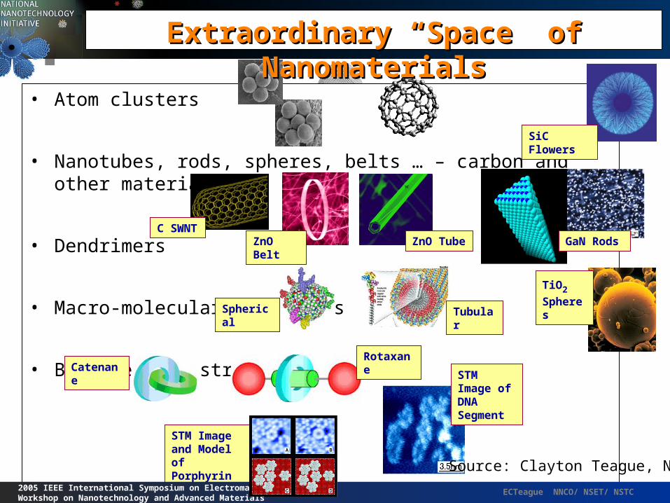
• Atom clusters
• Nanotubes, rods, spheres, belts … – carbon and other materials
• Dendrimers
• Macro-molecular structures
• Biomolecular structures
C SWNT ZnO
BeltZnO Tube
GaN Rods
SiC Flowers
TiO2
Spheres
STM Image of DNA Segment
Catenane
Rotaxane
Spherical
Tubular
STM Image and Model of Porphyrin
ECTeague NNCO/ NSET/ NSTC
2005 IEEE International Symposium on Electromagnetics Workshop on Nanotechnology and Advanced Materials
Extraordinary “Space” of NanomaterialsExtraordinary “Space” of Nanomaterials
Source: Clayton Teague, NNI

• 65 Minutes.....