Embed Size (px)
Citation preview

INSTRUCTION
Part No. 070-1735-00MANUAL
Product Group 26
TR 502TRACKINGGENERATOR
~ron~~coMnnirreo ro ExcFi_~Ervce
TEK MANUAL T~ON
First Printing NOV 1975Revised AUG 1984
TR 502
Part No._.070-1735-00Product Group 26
TRACKINGGENERATOR
Please Check for CHANGE lNFORMATlON at the Rear of This Manual
'Tronix®
Copyright © 1975 Tektronix, Inc . All rights reserved .Contents of this publication may not be reproduced inany form without the written permission of Tektronix, I nc .
Products of Tektronix, Inc . and its subsidiaries arecovered by U.S . and foreign patents and/or pendingpatents .
TEKTRONIX, TEK, SCOPE-MOBILE, and
areregistered trademarks of Tektronix, Inc . TELEQUIP-MENT is a registered trademark of Tektronix U.K .Limited .
Printed in U.S.A . Specification and price changeprivileges are reserved .

SECTION 5 CIRCUIT DESCRIPTION
TABLE OF CONTENTS
SECTION 8 ELECTRICAL PARTS LIST
Block Diagram Description
5-~
SECTION 9 DIAGRAMSandCIRCUITDetailed Circuit Description
5-1RF and Microwave Circuits
5-1
BOARD ILLUSTRATIONS
Bias Circuitry and Leveling Loop
5-2Phase Lock Loop
5-3
SECTION 10 MECHANICAL PARTS LIST
Operational Logic
5-4Power Supply Regulators
5-4
CHANGE INFORMATION
TR 502
SECTION 1 GENERAL INFORMATION
Page
SECTION 6 MAINTENANCE
PageAND SPECIFICATIONS
INSTRUCTIONS
Introduction
1-1
Preventive Maintenance
6-1Description
1-1
Cleaning
6-1ELECTRICALCHARACTERISTICS 1-2
Lubrication
6-1ENVIRONMENTAL
Visual Inspection
6-1CHARACTERISTICS
1-2
Transistor and IC Checks
6-1ACCESSORIES
1-2
Performance Checks andINSTALLATION
1-2
Recalibration Schedule
6-1REPACKAGING FOR SHIPMENT
1-3
Troubleshooting
6-2
SECTION 2 OPERATING INSTRUCTIONS
Troubleshooting Aids
6-2Diagrams
6-2Introduction
2-1
Circuit Board Illustrations
6-2About the Tracking Generator
2-1
Wiring Color Code
6-2Function of the Front Panel
Connectors
6-2Controls and Connectors
2-1
Capacitor Marking
6-2Operational Check
2-1
Diode Code
6-2
SECTION 3 PERFORMANCE CHECK
Transistor and IntegratedCircuit (IC) Electrode
Introduction
3-1
Configuration
6-2Preliminary Preparation
3-1
Finding Faulty Semiconductors
6-2Check Frequency Range
3-1
Diode Checks
6-3Check RF OUT Amplitude Range
3-1
IC Checks
6-4Check Flatness
3-1
General TroubleshootingPerformance Checks Which
Techniques
6-4Require Test Equipment
3-1
Corrective Maintenance
6-5Equipment Required
3-1
Obtaining Replacement Parts
6-5Check Amplitude Range
3-1
Parts Repair and ExchangeCheck Output Flatness
3-1
Program
6-5
Check Auxiliary Output Power
3-2
Soldering Technique
6-5
Check Residual FM
3-2
Transistor and IC Replacement
6-5Check for Spurious Signals
3-2
Replacing Square Pins for theMultipin Connectors
6-6SECTION 4 CALIBRATION PROCEDURE
Interconnecting Cable and Pin
Complete or Partial Calibration
4-1
Replacement
6-6
Adjustment and Test Point
Replacing Assemblies
6-6
Locations
4-1
Replacing Microwave
History Information
4-~
Assemblies
6-6
Equipment Required
q-1
Replacing the 2.2 GHz FourCavity Filter or Mixer
Preliminary Preparation
4-1
Assemblies
6-752.5 MHz Oscillator Mode Adjust 4-2Adjusting the NormalizingAttenuator
4-3
SECTION 7 OPTIONS and MODIFICATIONSOutput Level Calibration
4-3Sweep Trigger Level Adjustment 4-3

Fig . 1-1 . TR 502 Tracking Generator .

Introduction
Section 7-Options and Modifications: Provides dataThe abbreviations, graphic symbols, and logic sym-
on production options available.bology used in the text and diagrams of this manual are inaccord and based on ANSI Y1 .1-1972, ANSI Y32.2-1970,and ANSI Y32 .14-1973 (American National Standard
Section 8-Electrical Parts List : Provides informationInstitute, 345 East 47 Street ; New York, N.Y . 10017) .
necessary to order replaceable parts and assembliesrelated to the electrical functions of the instrument .
Change information has been integrated into themanual by goldenrod insert pages at the back of themanual and page revision . Original pages are identified bythe symbol @ and revised pages are identified by arevision date in the lower inside corner of the page . If theserial number of your instrument is lower than the oneonthe title page, the manual contains revisions that may notapply to your instrument. History or backlog informationall previously applicable to produced products with theupdated data is integrated when the page or diagram isrevised. The fol lowing describes the sections and informa-tion provided in this manual .
Section 1-General Information and Specifications :Contains instrument description, electrical specifications,environmental characteristics, accessories, installation,and repackaging for shipment instructions .
Section 2-Operating Instructions : Information relativeto operating and checking the instrument operation .
Section 3-Performance Check: Procedure to checkthe operational performance and electrical specificationsof the instrument . Two-part section provides an incominginspection type check and a detailed electrical perfor-mance verification .
Section 4-Calibration Procedure: Describes test
descriptionequipment setup and adjustment procedures required to
The TR 502 Tracking Generator operates with the 7L13calibrate the instrument .
or 7L12 Spectrum Analyzer to provide a calibrated rt signalfor swept frequency applications from 100 kHz to 1 .8 GHz.
Section 5-Circuit Description : Provides basic and
The output frequency of the TR 502 can be adjusted to
general circuit analysis that may be useful when servicing
track the spectrum analyzer frequency within 10 Hz . The
or operating the instrument .
TR 502, a two-wide unit compatible with the TM 500 Modu-lar Series instruments, is normally used with the TM 503(Option 07) Power Module . This permits the optional use of
Section
6-Maintenance
Instructions :
Describes
a digital counter such as the DC 508A with Option 07 . Aroutine and corrective maintenance procedures with
bright dot, on the spectrum display, identifies the frequencydetailed
instructions
for
replacing
assemblies,
sub-
location on the sweep that is indicated by the counter. High-assemblies, and individual components . An exploded
er range counters to 1 .8 GHz can be used by connectingdrawing is part of Section 10 .
their input to the TR 502 AUX RF OUT connector.
REV DEC 1981
GENERALINFORMATION ANDSPECIFICATIONS
Section 1-TR 502
Section 9-Diagrams : Provides functional blockdiagram and detailed circuit schematics . Located adja-cent to the diagram (usually on the back of the precedingdiagram) are pictorial layout drawings which show sub-assembly and component locations. Voltage and signallevel information, if applicable, is included to aid introubleshooting.
Section 10-Mechanical Parts List, Exploded Drawingsand Accessories: Provides information necessary to orderreplaceable mechanical parts . The Parts List is cross-referenced to the Electrical Parts List when appropriate .Exploded drawing shows sequence of assembly andidentifies assemblies .
Changes and Corrections : Provides updating informa-tion for the manual in the form of inserts . These inserts areincorporated into the manual text and diagrams when themanual is updated .

General Information and Specifications-TR 502
The following characteristics and features apply to theTR 502 and TR 502/7L13 Spectrum Analyzer system .They are applicable over the environmental specificationlimits for the TM 500- and 7000-Series mainframes .
Frequency Range:
TheTR 502 tracks the 7L13 tunedinput frequency from 100 kHz to1 .8 GHz.
Output Level : Two coaxial cables, 50 f2
Maximum Out-
0dBm ±0.5 dB .put Position
28.5 inchesLogic Interface Cable
(0 dBm) :
Adapter, "N male toBNC female"
Range:
0 to -59 dBm in 10 dB and 1 dB
Adapter, SMA Male tosteps .
BNC FemaleRetainer Plug-in
Relative Level
±0.2 dB/1 dB step to a maximum Manual, InstructionAccuracy :
of ±2.0 dB . A front panel controlprovides an additional 2 dB of
Optional Accessories
attenuation .
10 dB attenuator
Output Impedance :
50 S2 nominal, VSWR is 2:1 or lessto 1 .8 GHz .
Flatness :
ELECTRICAL CHARACTERISTICS
TR 502:
Within ±0 .65 dB, from 100 kHz to1 .8 GHz.
TR 502/7L13
Within ±1 .65 dB, from 100 kHz toSystem :
1 .3 GHz and within ±2 dB to 1 .8GHz.
Dynamic Range:
TR 502/7L13
110 dB or more .System :
Residual FM (peakto peak) : Installation
TR 502:
1 Hz or less . This instrument may be shipped installed in theTR 502/7L13 :
10 Hz or less .
TM 500-Series Power Module and ready for use as abench instrument, or it may be shipped as an individual
Auxiliary Output :
0.1 V rmsminimum, into 50 i2load .
unit. The instrument is held in the mainframe by means ofa mounting screw and shoulder washer through an
Spurious Output :
existing hole in a bottom cross-member . The retainerscrew threads into a bracket that is mounted on the back
Harmonic
20 dB or more below the carrier.
of theTR 502. (See list of accessories on ACCESSORIESContent:
tab page at the back of this manual.) Removethis screw to
Non-Harmonic
40 dB or more below the carrier.
free the TR 502 from the mainframe. If shipped as an
Content:
individual unit, install the bracket assembly by removingthe two center screws at the rear of the TR 502 and use
ENVIRONMENTAL CHARACTERISTICS
them to mount the bracket; install the TR 502 into theTM 500 Power Module as illustrated in Fig. 1-2. Afterinstallation, connect the TM 500 to a suitable power
This instrument will meet the electrical characteristics
source and proceed as directed in the Operating Instruc-
over the environmental limits of the TM 500-Series Test
tions section of this manual .
and Measurement System Power Module . Completedetails on test procedure, including failure criteria, etc.,can be obtained from Tektronix, Inc. Contact your localTektronix Field Office or representative .
Operating and Storage Requirements :
Operating Temperature Range:
0°C to +55°C.Storage Temperature Range:
-54°C to +75°C.
ACCESSORIESStandard Accessories
Refer to the Replaceable Mechanical Parts Section for partnumbers of standard and optional accessories.
Initial Inspection
INSTALLATION
This instrument was inspected both mechanically andelectrically before shipment . It should be free of mars orscratches and electrically meet or exceed allspecifications . To confirm this, inspect the instrument forphysical damage incurred in transit and test the electricalperformance by following the Operating Instructions inSection 2 and Performance Check Procedure in Section 3.If there is damage or deficiency, contact your localTektronix Field Office or representative .
REV . A, MAY, 1978
If the Tektronix instrument is to be shipped to aTektronix Service Center for service or replacement,attach a tag showing ; owner (with address) and the nameof an individual at your firm that can be contacted, pluscomplete instrument serial number and a description ofthe service required .
General Information and Specifications-TR 502
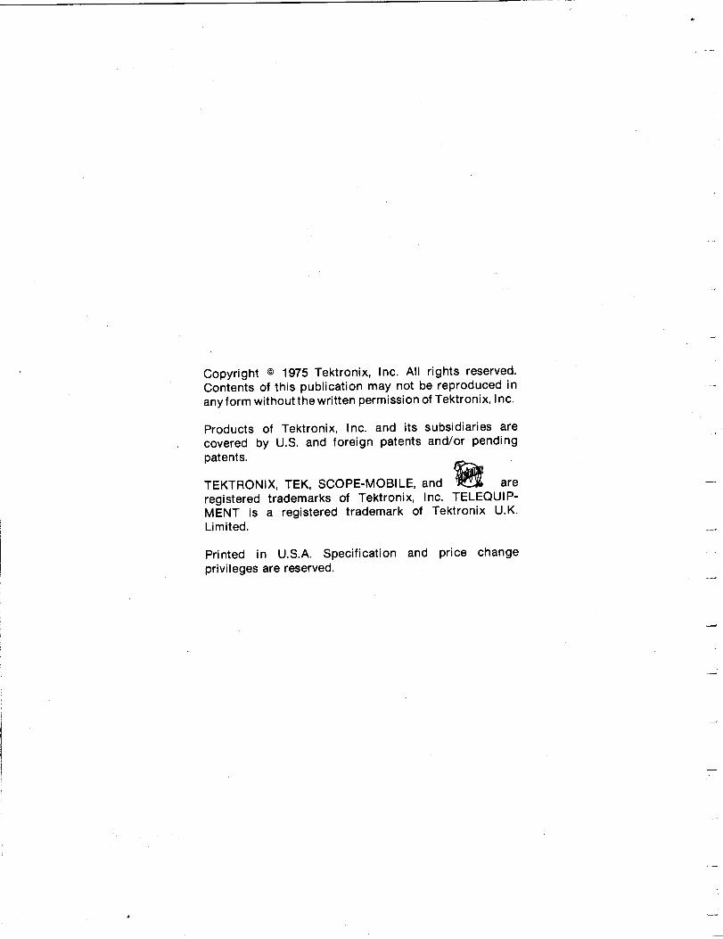
Fig . 1-2 . Plug-in Module Installation/Removal .
1735-2
REPACKAGING FOR SHIPMENT
2 . Wrap the instrument in heavy paper or polyethylenesheeting to protect the finish of the instrument . Protect thefront panel with urethane foam or cardboard strips .
3 . Cushion the instrument on all sides by tightlypacking dunnage or urethane foam between the cartonand the instrument, allowing three inches on all sides .
4 . Seal the carton with shipping tape or an industrialstapler .
Save and re-use the shipping container your instru-
TABLE 1-1ment was shipped in . If the original packaging is notavailable or unfit for use, repackage as follows :
Gross Weight (Ib)
Carton Test Strength (Ib)
10-30 27530-120
3751 . Obtain a shipping container made of heavy cor-
120-140
500rugated cardboard or wood with inside dimensions of no
140-160
600less than six inches more than the instrument dimensions ;this will allow room for cushioning . Refer to Table 1-1 for
If you have any questions, contact your local Tektronixcarton test strength requirements .
Field Office or representative .

Introduction
VAR dB : This control provides continuous output level
This section describes the function of the front panel
adjustment over a range of 2dB ; itaffects both the RF OUT
controls and connectors, installation of the TR 502 into
and AUX RF OUT levels .
the TM 500-Series mainframe, interface connections tothe
spectrum
analyzer
and
frequency
counter,
ad-
DOT INTENSITY: This control sets the brightness of the
justmentsrequiredtocalibratetheTR 502 to the spectrum
displayed frequency indicating dot when the TR 502 is
analyzer, and how to use the tracking generator.
used with a DC 502 Option 7, or equivalent frequencycounter, and the TR 502/7L13 Spectrum Analyzer isoperating in the sweep stop mode .
About the Tracking Generator
The TR 502 Tracking Generator is a two wide plug-inunit for the TM 500-Series (Option 7) Power Modules . Itoperates with the 7L13 or 7L12 Spectrum Analyzer toprovide a constant, level-calibrated rf signal source, thatprecisely tracks the spectrum analyzer input frequencyfrom 100 kHz to 1 .8 GHz. Signal output level is calibratedand adjustable from 0 dBm to -59 dBm in 1 dB steps. TheSpectrum Analyzer/Tracking Generator system can beused to display frequency response of carious devicessuch as filters, amplifiers, etc . that are connected betweenthe tracking generator RF OUTput and the spectrumanalyzer rf input connector.
When theTR 502 is installed in a modified three-wide or
AUXRF OUT: Asource of the output signal for auxiliarylarger, power module, a frequency counter such as the
test equipment such as a frequency counter. ThisDC 502 can be connected to the AUX OUT and used to
output connector must be terminated in a50 S2 load toaccurately measurethefrequencyforanyfixedpositionof
maintain flatness .span . When the analyzer is in the non-sweep mode, theTR 502 output is a cw signal and the counter readscontinuously . If a DC 502 Option 7, or similar counter is
INPUT CONNECTORS :used, the TRACKING GEN LOGIC is interfaced with the7L13 Spectrum Analyzer so operational logic from the
1st LO IN and 2nd LO IN : These interface to theTR 502 controls the sweep function of the spectrum
spectrum analyzer 1 st LO and 2nd LO Output connecanalyzer and the frequency counting of the counter. A dot
tors.i s displayed at sweep center to indicate where and whenthe frequency count is taken .
TRACK GEN LOGIC: Interfaces operational logicbetween the tracking generator and the spectrum
TheTR 502 is installed in theTM 500-Series mainframe
analyzer to operate the system with a compatible
by aligning the upperand lower guide rails with the plug-in
frequency counter.compartment tracks and pushing the TR 502 into thecompartment until the front panel is flush with themainframe front panel . To remove, pull the release latch todisengage the locking mechanism and pull t(~e unit out.
Operational Check and Calibration
See Fig . 1-2.
The TR 502 plugs into and receives its power from aTM 500-Series mainframe. It operates with the 7L13 or7L12 Spectrum Analyzer . The 1st and 2nd LO signal from
Function
of
the
Front
Panel
Controls
and
the spectrum analyzer are applied, via coaxial cables, toConnectors
the 1st and 2nd LO INput connectors for theTR 502. If the
The following is a description of the controls and
TR 502/7L13 system is used with a DC 502 Option 7
connectors on the TR 502:
Digital Counter, a third cable interfaces between theTR 502 and 7L13 Spectrum Analyzer to supply the
OUTPUT LEVEL: Selects 0 dB to 59 dB of attenuation in 1
necessary logic data for the various counter and spectrumdB steps of the calibrated output signal to the RF OUT ; it
analyzer operating modes. This interface cable is usedhas no effect on the output level of the AUX RF OUT.
when a counter is part of the system .
REV. A, MAY, 1978
OPERATINGINSTRUCTIONS
Section 2-TR 502
TRACK ADJUST: Adjusts the frequency offset betweenthe TR 502 Tracking Generator output signal and thetuned input frequency of the spectrum analyzer .
OUTPUT CONNECTORS :
RF OUT: A 0 dBm to -61 dB, 50 S2, signal source with afrequency, that tracks the spectrum analyzer . Outputlevel depends on the setting of OUTPUT LEVEL andVAR dB controls .
2-7

Operating Instructions-TR 502
1 .
Preliminary
c. Set the spectrum analyzerSpan/Divto Max, Resolu-
a.
Insert the TR 502 in a TM 500power unit mainframe
Lion to 3 MHz, Display Mode to 10 dB/Div, Reference
(TM 500Option 7) and the spectrum analyzer (7L13) into a
Level to 0 dBm, and switch on the power to all units.
7000-Series mainframe .
b .
Using the coaxial cables, supplied with the standardaccessories, connect the 1st and 2nd LO Output ports ofthe spectrum analyzer to the 1 st and 2nd LO Input ports of
2.
Check Output Levelthe TR 502, then connect the RF OUT to the RF Input ofthe spectrum analyzer . If a frequency counter is used,
a . Change the spectrum analyzer Reference Level to
connect the AUX RF OUTput of the TR 502 to the RF Input
0 dBm. Set the TR 502 OUTPUT LEVEL and VAR dB
of the counter. Fig . 2-1 illustrates system hookup .
controls for an output of 0 dBm (fully clockwise) .
2-2
FREQUENCYCOUNTER
AUXRF
RF
\" /
" .
OUTOUT
TRACK GEN
RF
"
TRACKINPUT ~1 LOGIC
IN
GEN
N-TO-BNCADAPTER
TR502
3mm, SMA-TO-BNCADAPTER
2nd LO
7st LO
d. Set the OUTPUT LEVEL of the TR 502 to -10 dBmand check for a level (±3 dB) across the spectrumanalyzer display (100 kHz to 1 .8 GHz) .
Fig. 2-1 . TR 502/7L13 Spectrum Analyzer System with a Frequency Counter.
aooo00000 0
0
1735-3A
REV. A, MAY, 1978

e. Rotate the VAR dB control through its range andnote that the display level decreases in accordance withthe calibrated scale on the front panel . Return the controlto its 0 dB position and/or the spectrum analyzer Ref Varcontrol to Cal .
a . Set the spectrum analyzer Reference Level to+10 dBm and the Display Mode to 2 dB/Div . Set theTR 502 OUTPUT LEVEL and VAR dB controls for anoutput of 0 dBm (fully clockwise) .
b. Decrease the spectrum analyzer Freq Span/Divtowards 200 Hz while adjusting the TRACKING ADJUSTcontrol for minimum frequency offset . This correspondsto maximum response on the display. .
REV . A, MAY,1978
NOTE
Operating Instructions-TR 502
b. Decrease the TR 502 OUTPUT LEVEL to -50 dBm
Measuring Frequencyin 10 dB increments and increase the spectrum analyzer
The TR 502 features a sweep-stop operational modesensitivity in 10 dB increments . Note that the display level
that stops the sweep at center screen, centers the dot,remains constant .
instructs the frequency counter to take a frequencymeasurement, then allows the sweep to continue . Gate
c. Return the TR 502 OUTPUT LEVEL to 0 dBm,
(count) time is determined by the phase lock mode of theanalyzer . When the analyzer is phase locked, the frequen-
change the spectrum analyzer Freq Span/Div to 1 MHz
cy count is accurate to the nearest 10 Hz and when theand the Display Mode to 2 dB/Div . Adjust the spectrum
analyzer is not phase locked the accuracy of the count is toanalyzer Ref Var control or the TR 502 VAR dB control to
the nearest 100 kHz. This sweep-stop mode can beset the display at some graticule division .
switched off by the DOT INTENSITY control . Logic data,to stop the spectrum analyzer sweep and operate the
d . Decrease the TR 502 OUTPUT LEVEL in 1 dB steps
counter, is transmitted through the interconnecting cablebetween the TRACK GEN LOGICconnectors and the data
and note that the display level decreases proportionately.
lines between the interface connectors of the TM 503Return theOUTPUT LEVELandVAR dB control to 0 dBm.
Option 7, orother compatible TM 500-Series mainframes .
In the non-sweep (Manual or External) the count iscontinuous . If the TR 502 is used with a 7L12 SpectrumAnalyzer, or the frequency counter is not compatible withthe operational logic of theTR 502, the analyzer should beoperated in the non-sweep modes to measure frequency.
3. Tracking Adjust
Connect and operate the system as follows:This control adjusts theTR 502outputfrequencytothe
input frequency of the spectrum analyzer .1 . Connect the AUX RF OUTthrough a 50 S2 cable to
the frequency counter Input. If the system has theTracking Generator Logic feature, connect the logicinterface cable to the TRACK GEN LOGIC connectors .Note : TM 500-Series mainframe must have the data linesbetween the interface connectors (Option 7 for TM 503) .
2. Turn the power on and set the VAR dB control tozero .
3. With the 7L13 in the sweep mode, turn the DOTINTENSITY on and adjust the brightness level of thefrequency dot.
4. Counter should now indicate the frequency of thedot .
NOTEIf the TR 502 is used with a 7L13 Spectrum Analyzerthe TRACKING ADJUST may run out of range at
The sweepstop trigger level of the TR 502should behigh resolution (3 kHz or less) settings because the
adjusted to match the 7L13 center screen level.IF in some early production 7L13 units maydeviate a
Accuracy of the dot is not affected however. If a holesmall amount from 105 MHz. If this occurs, notify or
exists between the sweep stop point and the dot, itcontact your local Tektronix Field Office or
can be removed by referring to the Calibrationrepresentative to correct this situation .
section for adjustment procedure.
2-3
WARNING
THE FOLLOWING SERVICING INSTRUCTIONSARE FOR USE BY QUALIFIED PERSONNELONLY . TO AVOID PERSONAL INJURY, DO NOTPERFORM ANY SERVICING OTHER THAN THATCONTAINED IN OPERATING INSTRUCTIONSUNLESS YOU ARE QUALIFIED TO DO SO .REFER TO OPERATORS SAFETY SUMMARY
AND SERVICE SAFETY SUMMARY PRIOR TOPERFORMING ANY SERVICE.
3. Check RF OUT Amplitude Range
PERFORMANCE CHECK
Introduction
d. Reduce the OUTPUT LEVEL from 0 dBm toThis section contains two parts: An operational check-
-50dBm in 10 dB steps while changing the spectrumout procedure, for incoming inspection and instrument
analyzer Reference Level from 0 dBm to -50 dBm . Thefamiliarization (this requires no test equipment) . And a
display level should return to the original reference level
performance check procedure, that requires test equip-
(within ±1 .0 division) after each step .ment as the measurement standard to verify instrumentspecifications such as output level and flatnesscharacteristics . The latter portion can be used to deter-
4. Check Flatnessmine if the instrument needs repair or recalibration.
a . Set the spectrum analyzer Freq Span/Div to MaxSpan with the Resolution control coupled (3 MHz) . Leavethe vertical display at 2 dB/Div and the Reference Level at
1 . Preliminary Preparation
0 dBm.
Connect the TR 502 to the 7L13 and/or 7L12 SpectrumAnalyzer and perform the preliminary front panel set-upprocedures and calibration described in the OperatingInstructions .
c.
Observe the display flatness . Display should be flat(within ±1 division or±2 dB) over the 100 kHzto 1 .8 GHz
2. Check Frequency Range
span (see Fig. 3-1) . Disregard the spectrum analyzer 0 Hza . Set the spectrum analyzer Reference Level to 0 dBm
response at the left edge of the display.by inserting rf attenuation . Set the vertical display to10 dB/Div, the Span/Div to Max Span with the Resolutioncoupled (3 MHz) and switch the Phase Lock on . Set the
PERFORMANCE CHECKS WHICHTR 5020UTPUTLEVELtoO dBm with theVAR dB control
REQUIRE TEST EQUIPMENTat 0 . Connect the TR 502 RF OUT to the 7L13 or 7L12 RFInput by means of a short 50 S2 coaxial cable.
b . The display should be a horizontal line near fullscreen amplitude over the full 1800 MHz span across thescreen .
a. Set the spectrum analyzer Center Frequency to500 MHz. Set the Freq Span/Div to 5 MHz with theResolution coupled . Switch the Display Mode to 2 dB/Divand leave the Reference Level at 0 dBm.
b. Reduce the TR 502 OUTPUT LEVEL setting from0 dBm to -9 dBm in 1 dB steps. Display level on thespectrum analyzer should drop by 4.5 ±1 division (9 dB±2.0 dB) .
b. Set the TR 502 OUTPUT LEVEL to -10 dBm.
Introduction
The following procedures check the amplitude rangeand accuracy, TR 502 output flatness, residual FM, aux-iliary output level, and output level of spurious signals.
Equipment Required
Section 3-TR 502
a. Power Meter: Measurement range up to 0 dBm .General MicrowaveMode1454AorHewIettPackardModel435A with 8482A Power Sensor .
b. Test Spectrum Analyzer : Tektronix 7L13 or 7L12 .
c. Mainframe for Spectrum Analyzer : Tektronix 7000-Series with storage; such as 7613 .
c . Rotate the VAR dB control through its full range.
1~ Check Amplitude Range and Output FlatnessThe display level on the spectrum analyzer should change
a. Set the spectrum analyzer Center Frequency toabout 1 division . Return the VAR dB control to its 0 dB
50 MHz and decrease the Freq Span/Div to 0 Hz so theposition .
frequency is not swept. Switch the Phase Lock on .

Performance Check-TR 502
b. Connect the TR 502 RF OUT to the power meter
b. Connect the TR 502 RF OUT to the input of a test
with a short length of 50 f2 coaxial cable . Set the VAR dB
7L13 or 7L12 Spectrum Analyzer . Set the test spectrum
control to 0 dB and theOUTPUT LEVELdBmselector to 0.
analyzer Reference Level at 0 dBm, the Freq Span/Div atThe power meter should indicate 0 dBm ±0 .5 dB .
200 Hz with the Resolution at 30 Hz . Adjust the TR 502output frequency with the spectrum analyzer so its outputis centered on the test spectrum analyzer display. Check
c. Reduce theOUTPUT LEVELdBm in 1 dB steps then
thedisplay for residual fm . Residual fm should not exceed
10 dB steps and check that the power meter reading
100 Hz with the 7L13 or 200 Hz with the 7L12 .
indicates the OUTPUT LEVEL, within 0.2 dB/dB step to amaximum of ±2.0 dB for the total 9 dB or 50 dB range.
d . Return the OUTPUT LEVEL dBm to 0andcheck theOUTPUT LEVEL at various frequency points throughoutthe 1 .8 GHz range.
e.
Power meter should indicate 0 dBm ±0.5 dB for allfrequency points checked.
4. Check For Spurious Signals
a. Leave the TR 502/Spectrum Analyzer system con-trols as previously set in step 3 and set the test spectrum
2. Check Auxiliary Output Power
analyzer controls as follows : Freq Span/Div to 20 MHz
a . Leave the spectrum analyzer controls as previously
with the Resolution coupled, Center Frequency 100 MHz,
set in step 1 . Connect the power meter to the TR 502 AUX
and Display Mode of 10 dB/Div .
RF OUT . Set the OUTPUT LEVEL dBm control to-10 dBm to terminate the RF OUT connector.
b. Check the harmonic related spurii (at 100 MHz,150 MHz, and 200 MHz) are at least 20 dB down from the
b. Tune the spectrum analyzer frequency over the
tracking generator output level at 50 MHz.100 kHz to 1 .8 GHz rangeandcheck that theAUXRF OUTpower is at least-7 dBm (0 .1 V rms into 50 S2) as indicatedon the power meter over the frequency range .
c. Tune the test spectrum analyzer frequency up to1800 MHz checking that all non-harmonic (not multiplesof 50 MHz) spurii are at least 40 dB down from the
NOTE
reference level at 50 MHz.
This specification is the minimum output level .Output varies with VAR d8 control setting. Instru-ment shouldput out-7d8m even with VARdB in thelow-power position .
3. Check Residual FM (peak to peak)
NOTE
Use a Freq Span/Div of 500 Hz with a Resolution of300 Hz when checking a 7L12/TR 502 System .
d . Tune the TR 502/Spectrum Analyzer system toother reference frequencies within the frequency rangeand check to ensure non-harmonic spurii are at least20 dB down from the reference.
a. Tune the spectrum analyzer frequency to 50 MHz.
This concludes the performance verification check for
Leave the Freq Span/Div at 0 Hz .
the TR 502/Spectrum Analyzer system .

CALIBRATION PROCEDURESection 4-TR 502
This section provides adjustment procedures and
Equipment Requiredinternal checks for the TR 502. After calibration, perform
The equipment that is required to recalibrate thisthe Performance Check in Section 3 to verify instrument
instrument includes the equipment listed for the Perfor-performance. The limits, tolerances and waveform il-
mance Check plus the following: ,lustrations in this procedure are aids to calibrate theinstrument and are not intended as circuit specifications .
DC Voltmeter or
0to 50 V range; Tektronix DM 501Multimeter :
of the TM 500-Series or a TriplettModel 630-PL .
Complete or Partial Calibration
The procedure is written in a logical sequence . If the
FrequencyCounter:
Frequency range to 60 MHz, shortinstrument is known to be completely out of calibration,
term stability 1 part in 10~; resolu-the sequence should be followed . The circuits, including
tion
200 Hz
@
52.5 MHz,
Tek-the microwave integrated circuits, for this instrument are
tronix 7D14 for the 7000-Series orvery stable . Complete calibration or recalibration may
a TM 500-Series Counter with Op,therefore be necessary only after a component has been
tion 01 .replaced or the instrument fails to meet performancerequirements. The Performance Check has been writtento lead you to the proper adjustment or circuit . We advise
Vertical Amplifier
Sensitivity 5 mV to 5 V. Bandwidthrecalibrating only those circuits that do not meet
Plug-In Unit :
50 MHz or better .specifications . Turn to the desired step and prepare theinstrument for calibration by referring to the preceding
1X Probe
Tektronix P6062A .setup and controls settings then adjust or calibrate as
(1pp MHz) :directed .
The 2.2 GHz four-cavity filter and mixer adjustmentsare only required if the filteror mixerassembly is replaced .The adjustment procedure for this filter is part of thereplacement instructions in the Maintenance Instructions(Section 6) of the manual .
10X Probe
Tektronix P6062A .(100 MHz) :
Plug-In Extender
Tektronix Part No . 067-0645-02.for TM 500:
Preliminary PreparationThe instrument should be cleaned and inspected, as
NOTEdescribed in the Maintenance section, before performinga complete calibration .
Instrument calibration should be performed with theambient temperature equal to the normal operating
Adjustment and Test Locations
temperature, after a warmup period, with power on,equal to the warmup requirements for the 7L13 or
Test point and adjustment locations are shown with or
7L12 to stabilize .adjacent to the written procedure. These points andadjustments are accessible with the outer covers removed .
History Information
The instrument and manual are periodically evaluatedand updated . If modifications require changes to thecalibration procedure, history information applicable toearlier instruments is integrated into or written as asubpart of the step .
Interaction
c. If adjustment of the 52.5 MHz Mode Adjust isAdjustments that interact with other circuits are noted
required, remove the cover plate to the honeycomband reference made to the affected circuit.
assembly to gain access to the mode adjustment .
REV DEC 1981
a. Check the front panel controls for smooth operationand proper indexing .
b. Turn the power to the TR 502 off. Remove theTR 502 from the TM 500 mainframe and connect itthrough a flexible plug-in extender to the mainframeinterface connector. Fig . 4-1 illustrates typical setup forcalibration . Turn the power on .

Calibration Procedure-TR 502
4-2
TM503
TUNING TOOL
RF OUT
D
POWER METER
1st LO IN
2nd LO IN
Fig . 4-1 . Setup for Calibration .
7000 SERIES OSCILLOSCOPE
1735-4
This adjustment is required only when tracking
Use a low-capacitance probe to minimize loading
accuracy is out of specifications or a frequency-
and connect the ground lead of the probe to the
determining component, such as the crystal or the
TR 502 chassis . Output of 05208 is approximately
IC (0520), has been replaced.
800 mV peak to peak .
1. 52.5 MHz Oscillator Mode Adjust
b. Adjust the Mode Adjust C524 (Fig . 4-2) so the
a. Connect a frequency counter, through a 1X probe,
52 .5 MHz
oscillator
starts
at
any
position
of
the
to receptacle K or W520 ; and the Input to a vertical
TRACKING ADJUST control as the power is turned off
amplifier, through a 10X probe, to receptacle K or W250
and on . (Power should be off long enough for the supply
(Fig . 4-2) .
voltage to decay before switching back on.)

Fig. 4-2. Location of receptacle K, w520, and C524 .
c. Check the frequency range of the TRACKINGADJUST and if necessary, adjust 0524 (Mode Adjust) sothe range is at least ±1 .0 kHz either side of 52 .5 MHz .
d . Replace the honeycomb cover then check theTRACKING ADJUST range to ensure that the trackingaccuracy is such that it tracks the 7L13 or 7L12 inputfrequency at the lowest resolution bandwidth settings(30 Hz for 7L13, 300 Hz for 7L12) .
2. Adjust the Normalizing Attenuator
NOTE
The range of this adjustment is broad. It should onlyrequire adjustment when fhe 2.095 GHz oscillaforand Amplitude Control assembly is replaced or theflatness is out of specification.
a. Set the spectrum analyzer Frequency Span/Div toMax and Time/Div to 10 ms .
b .
Adjust the Signal Level Normalization with 8215 for1 .5 V drop across R210 (Fig . 4-3) .
3. Output Level Calibration
a.
Apply the 50 MHz Calibrator signal to the spectrumanalyzer Input and tune the center frequency to 50 MHz.Reduce the Frequency Span/Div to 0 keeping the inputtuned to 50 MHz.
b. Remove the Calibrator signal to the analyzer andconnect a power meter (such as HP Model 435A) to theTR 502 RF OUT.
REV DEC 1981
Calibration Procedure-TR 502
c. Set the VAR dB control to -2 and adjust the MinOutput Level with 8225 (Fig.4-3) for-2 dBm output level .
d . Set the VAR dB control to 0 and adjust the MaxOutput Level with R220 (Fig . 4-3) for 0 dBm .
e .
Setthe VAR dB control to -1 and adjust theVAR dBLinearity with R222 (Fig . 4-3) for -1 dBm .
f.
Recheck the 0 and -1 positions because of interac-tion .
g. Check the output level calibration at -0.5 and -1 .5settings of the VAR dB control.
4. Sweep Trigger Level Adjustment
The Sweep Trigger Level is adjusted to match theTR 502 sweep stop trigger level to the 7L13 center screenlevel .
a. With the TR 502/7L13 and compatible frequencycounter (DC 502 with Option 7) connected as a systemand theTR 502 out of theTM 500 PowerModule compart-ment, on an extender cable, calibrate the 7L13 span so thecenter of the display is accurate (see 7L13 OperatingInstructions) .
Fig . 4-3. Location of Signal Level Normalisation AdjustmentR215, and Output Level Calibration Adjustments R225, R220,R222 .
4-3

Calibration Procedure-TR 502
Fig . 4-4 . Location of Trigger Level Adjustment .
b.
Set the 7L13 Freqeucney Span/Div to Max and turnthe TR 502 DOT INTENSITY control clockwise until thedot is visible on the analyzer display.
c.
Adjust the SweepTrigger Level R475 (Fig . 4-4) untilthe sweep stop point is next to the dot (Fig . 4-5) .
al *201d~ ~ 0~~7 art JI ~ +~~
(B) Sweep stop at center screen .
(A) Sweep stop prior to center screen .
Ar .
o r7
;rr
"" +
" " r"
This completes the calibration procedure for the
'
1735-sTR 502 . Verify its operation by the Performance Check inSection 3 .
Fig. 4-5 . How the sweep stop should align to the dot position .
CIRCUIT DESCRIPTION
This section describes the functions of the major
2.095 GHz oscillator and the phase-lock mixer circuit. Atcircuits and their relationship to each other. Thedescrip-
zero frequency the 1st LO is near 2.095 GHz which, iftion is general and is intended as an aid for the technician
allowed to feed back to the 2 .095 GHz oscillator, wouldand operator to facilitate servicing the instrument or
disable the phase-lock operation . The 6 dB attenuatoroperating it to its fullest capabilities . The section starts
provides the proper impedance termination into thewith a block diagram description, followed with a more
output mixer to reduce the effects of output impedancedetailed analysis of the major circuits . Thediagrams may
characteristics of the isolation amplifier.contain typical waveforms, voltage data, and signal levelsfor full screen display, to help understand circuit functionsand aid in troubleshooting .
The conversion loss through the output mixer isconstant with frequency. The amplitude level of the IFsignal tracks the amplitude of the rf signal with about 6 dB
BLOCK DIAGRAM DESCRIPTION
to 8 dB of loss . The IF level is therefore set by controllingthe rf input level . A constant output level is maintained bymeans of a feedback loop that controls the attenuation in
The spectrum analyzer (7L13 or 7L12) up-converts its
the 2.095 GHz signal path . The forward signal pathinput signal frequency to a 1st IF of 2.095 GHz, by the 1st
through the attenuator affects the signal level at the levelLO (local oscillator) frequency, then down-converts this
detector. The feedback path applies this level to the2 .095 GHz by the 2nd LO frequency to obtain an IF of
leveling attenuator as a correction signal so the output105 MHz. The TR 502 Tracking Generator reverses this
remains constant over the frequency range of the instrusequence to generate an output signal with a frequency
ment.equal to the input frequency to the spectrum analyzer . Forexample: an input signal frequency of 900 MHz to thespectrum analyzer is up-converted to 2.095 GHz by the
The input signal from the 1 st LO is 3 mW or more . Thismixing action with the 1st LO frequency of 2.995 GHz.
is amplified by the 2.1 GHz to 3.9 GHz amplifier so theThis signal
is then converted down to 105 MHz by
level into the LO port of the output mixer is between 5 mWheterodyning the 2.095 GHz with the 2nd LO signal
to 10 mW. Harmonics of the input signal frequencies arefrequency of 2.2 GHz. The TR 502 Tracking Generator
attenuated by the 2.1 GHz to 3 .9 GHz bandpass filter . Re-converts a 105 MHz reference signal to 2.095 GHz by
entrant modes of the bandpass filter are eliminated by ausing the 2nd LO signal (2 .2 GHz) in a phase-lock loop .
low-pass filter . Good termination for the amplifier andThis 2 .095 GHz is then mixed with the 1st LO signal of
bandpass filter is provided by the two isolators . Isolation2.995 GHz to generate an output of 900 MHz.
between the output mixer and the 1 st LO is provided by thetwo isolators and the amplifier. This isolation and the filterprevent signals in the 0 to 1 .8 GHz and 4.2 GHz to 6 GHz
The tracking generator 2.095 GHz oscillator is phase-
rangefrom getting back into the spectrum analyzer . Theselocked 105 MHz below the spectrum analyzer 2nd LO
signals, if allowed to feed back to the spectrum analyzer,
frequency. This difference frequency, from the mixer, is
would degrade the analyzer sensitivity and cause themaintained at 105 MHz by dividing it down to 52.5 MHz
baseline of the display to lift .and comparing this to a 52.5 MHz crystal-controlledoscillator . A voltage that is proportional to the phasedifference is fed back as an error signal to keep the
The operational logic interfaces the TR 502 to the2.095 GHz voltage-controlled oscillator offset 105 MHz
spectrum analyzer and an external digital counter. Thisbelow the 2nd LO input signal .
logic controls the sweep function of the spectrum analyzerand the frequency counting function of the frequencycounter for the various modes of operation .
The 2.095 GHz signal is passed through a directionalcoupler which couples some of the signal to the phase-
DETAILED DESCRIPTIONlock loop and directs the remaining energy through anormalizing attenuator (which establish amplitude level) a2.2 GHz low-pass filter (to attenuate harmonicsand upper
RF and Microwave Circuits
sidebands from the output mixer), a second leveling
TheRF section consists of microwave assemblies thatattenuator, an isolation amplifier, and a 6 dB attenuator
include microwave integrated circuits in metal enclosuresinto the output mixer. The isolation amplifier prevents
Because repair of these assemblies requires specialenergy, from the output mixer; feeding back into the
techniques and equipment we recommend replacing the
Section 5-TR 502
Circuit Description-TR 502
entire assembly if it should fail . The diagrams for these
The 2.095 GHz signal is fed from the directionalassemblies show only the basic configuration and il-
couplertoaPINdiodeattenuatorwiththediodeoperatinglustrate their function and do paths between the external
as a variable resistor . The circuit is basically a "T" typeconnectors .
attenuator with the resistance of the diode the inverse ofthe current . As the current increases the diode resistancevaries from open circuit to about 5 S2 (current increase
The input signal from the spectrum analyzer 1st LO is
from 0 to about 5 mA). This variable allows for the initialamplified to a level of about 10 mW by the 2.1 GHz to
adjustment of the output level range.3.9 GHz amplifier. Gain of the amplifier is nominally 6 dB .Because of gain characteristics, this amplifier operates asa limiter and provides a relatively constant output over a
The 2.2 GHz low-pass filter attenuates harmonics ofwide range of input signal levels . This limiting action
the 2.095 GHz frequency in the forward direction, andprovides a constant LO signal level to the output mixer
higher frequencies (i .e ., 2.2 GHz and higher) that getwhen the TR 502 is interfaced with different spectrum
through the isolation amplifier from the output mixer.analyzers .
The 2 to 4 GHz isolators have less than 0 :4 dB loss inthe forward direction and more than 20 dB loss in thereverse direction . The 4.5 GHz low-pass filter is a tubulartype filter used to attenuate the re-entrant mode of theinterdigital bandpass filter (third multiple of its pass-band). This bandpass filter attenuates harmonics of2 .1 GHz to 3 .9 GHz signals that are generated by thespectrum analyzer and the saturated 2.1 GHz to 3.9 GHzamplifier. This filter also attenuates any 0 to 1 .8 GHz and4.2 GHzto6 GHzsignals that return from the output mixerof the TR 502.
The mixer requires about 5 mW into the LO port and anominal -24 dBm into the rf port . The IF output of themixer is about -30 dBm over the frequency range of 0 to1 .8 GHz .
The 2nd LO signal from the spectrum analyzer isapplied through a 20 dB attenuator, a 2 .2 GHz low-passfilter, and a four-cavity bandpass filter to the mixer. The2.2 GHz low-pass filter attenuates or blocks the re-entrantmodes (6.6 GHz and 11 .0 GHz) of the multi-cavity band-pass filter . The pass-band of the filter is narrow enough toattenuate the 2 .095 GHz oscillator signal and prevent thissignal from getting back into the spectrum analyzer .Adjustment of the bandpass filter response is ac-complished by the four tuning screws, one foreach cavity .The signal then passes to a two-diode balanced mixerwhere it is mixed with the 2 .095 GHz oscillator signal . Themixer is adjusted for balance and coupling .
The 105 MHz IF signal from the mixer is passed througha directional coupler and an all-pass network to the105 MHz amplifier. The all-pass network terminates thehigh frequency energy that comes through the directionalcoupler.
The leveling attenuator is identical to the normalizingattenuator . The isolation amplifier gain is about 7 dB withgreater than 20 dB of reverse isolation . Its output drivesthe mixer through a 6 dB attenuator .
The lower conversion frequencies from the mixer passthrough a 3 dB attenuator and low-pass filter to thewideband amplifier. The 3 dB attenuator provides awideband (to 6.6 GHz) termination for the mixer. The low-pass filter attenuates 2 .095 GHz and its upper wdebandfrequency components (that come out of the mixer) fromreaching the wideband amplifier.
The low-pass filter is flat to 1 .8 GHzand rolls off with asharp notch at 2.095 GHz. The 0 to 1 .8 GHz signal is thenamplified about 40 dB by the wideband amplifier, thenpassed through another 1 .8 GHz low-pass filter to thepower divider and level detector .
The second 1 .8 GHz low-passfilterattenuatesfrequen-cies above 1 .8 GHz which may be generated by theamplifier. Harmonic distortion increases as the signalfrequency or level increases.
The level detector is a directional peak detector thatsenses the forward power but not the reflected or reversepower. Forward power i,s independent of the load . Powerloss through the divider to the RF OUT connector is about6 dB and 9 .5 dB to the AUX RF OUT connector. Power atthe AUX RF OUT port is therefore about 3.5 dB below thepower at the RF OUT port . The output attenuator providescalibrated 1 dB and 10 dB steps of output power to the RFOUT connector.
Bias and Leveling Loop Circuitry
The 2.095 GHz oscillator uses a resonant micro-strip
Bias for the amplifiers, in the microwave assembly andlinein.thecollectorofacommon-base transistor oscillator
the isolation amplifier, is supplied by five bias suppliesto establish its frequency . It is tuned (about 20 MHz) by
(U150, U160, U170, U180, and U240) on the Bias circuitvarying the collector voltage to change the collector-to-
board. The bias circuits and amplifier are connected as abase capacitance .
feedback loop with the collector load current of the

amplifier sensed as a voltage by the input resistor (R ;) tothe operational amplifier . This voltage is compared to a+10 V reference . The amplifier output drives the base ofthe rf amplifier to set the bias . The collector voltage istherefore held constant at+10 V . The load resistors fortheoutput amplifiers are R140, R162, R174, and the resistor inthe microwave assembly for the last amplifier stage . Theseresistors set the collector currents of the first twoamplifiers at about 10 mA, the third at 20 mA, and the lastat 30 mA. The load resistor for the isolation amplifier isR242 . Collector current is about 15 mA .
The +10 V reference for the bias circuits is generatedby a voltage regulator circuit using an operationalamplifier U250 . The reference for the regulator is a 6 .2 VZener diode VR258, which sets the voltage level at theinverting input of the amplifier . The amplifier boosts thisvoltage to +10 V . The +10 V supply provides the biascurrent for the 6.2 V Zener . A 7.5 V Zener (VR250) isconnected from the output to the +15 V supply to start theregulator . As soon as the output of the regulator exceeds7 .5 V the Zener diode no longer draws current and doesnot affect regulator operation .
Phase Lock Loop
Circuit Description-TR 502
The 2.095 GHz oscillator in the TR 502 is phase locked105 MHz below the 2.2 GHz signal from the spectrumanalyzer . The difference signal (105 MHz) from the mixeris amplified through four amplifier stages, then divideddown to 52.5 MHz and compared with 52 .5 MHz crystal-controlled oscillator signal . A voltage that is proportionalto the phase difference is fed back to correct the phase ofthe 2.095 GHz oscillator so that its resultant output islocked 105 MHz below the 2nd LO of the spectrumanalyzer .
U500 and U540 are differential amplifiers with emitterfollower outputs . The differential output of U500A drivesthe differential input of U500B and the output of U540Bdrives the differential input to U540A . Gain of each stage isabout 15 dB . The output level of the amplifier stagesremains relatively constant over an input level range from-45 dBm to +10 dBm . This output is applied to a divide-by-two counter (U550) and the resultant 52.5 MHz isapplied to the phase/frequency detector U545 for com-parison to the 52.5 MHz crystal-controlled oscillatorsignal .
Diode CR250, between the +15 V line and ground,
The reference 52 .5 MHz signal from the crystal-protects the microwave circuitry from any unintentional
controlled oscillator U520A is applied through a bufferapplication of negative voltage on the line .
stage (U520B) to the other input of the phase/frequencydetector . The crystal operates in its third overtone which is
The leveling
loop consists of a level detector and
selected by the low 0 resonant circuit tuned by C524 . Thetemperature-compensating diode driving a differential
frequency can be tuned through 52.5 MHz by C530 andamplifier . The output of the amplifier drives another
the voltage that is applied to the variable capacitanceamplifier
which
sets
the
attenuation
of
the
leveling
diode CR526 . Bias to the diode is varied by the front panelattenuator . The diodes are biased so their output is
TRACKING ADJUST control R10 . (Voltages for the ad-approximately +0 .4 V with no power into the detector . The
justment are supplied by U365B .) This control allows theoutput of the diodes drive the inputs of a differential
operator to set the TR 502 output frequency at theamplifier U200 . The output of the compensation diode is
spectrum analyzer inputfrequencyoroffsetthefrequencysummed with a voltage set by the leveling control circuit .
a slight amount .The temperature-compensating diode compensatesdetector output changes due to temperature . As the powerinto the detector increases, the output is an average
Theoutput of the detector is applied to a compensatingsignal, that is below +0 .4 V with the positive excursions of
amplifier U365A, 0420 . The compensating amplifier has athe signal clamped at +0.4 V .
buffered output that drives the collector of the 2 .095 GHztransistor oscillator . 0440 limits the output current if theoutput should inadvertently be shorted .
U200 is an operational amplifier configured as anintegrator . Its output is a correction signal which rangeseither in a positive or negative direction depending on the
Transistors 0445 and 0430 are the active componentsdifference
between
the
level detector voltage and
a
for a anti-latch circuit . This circuit, when activated, drivesreference voltage . This reference voltage depends on the
the compensating amplifier so its output tune voltageoutput of a voltage divider network, consisting of ad-
causes the 2.095 GHz oscillator to search through ajustments R225, R220, R222, and the front panel VAR dB
frequency band until it locks to the 2 .2 GHz, 2nd LOcontrol . Min Output Level adjustment R225, sets the offset
frequency, of the spectrum analyzer . When the tuneconstant or minimum level . Max Output Level adjustment
voltage drops to +3 V or less, 0445 is cut off . The collectorR220, sets the range of the VAR dB control to about 2 dB .
voltage rises towards Vcc and allows C432 to chargeThe VAR dB Linearity adjustment R222, shapes the
through R438 and R444 until it reaches 0.7 V above theresponse of the output level versus the rotation of the
gate potential of the programmable unijunction transistorcontrol so the dial is calibrated in dB . A 6.2 V Zener diode
0430. When the programmable unijunction transistor(CR262) sets the reference for the output level control
turns on, the charge on the capacitor C432 is transferredcircuitry .
to the cathode and through CR432 to the non-inverting
5-3

Circuit Description-TR 502
input of the operational amplifier and capacitor C428 . The
The phase lock logic line tells the counterhowaccurateoutput of the compensating amplifier steps positive to
to count. In the phase lock mode, .the count is to theabout +18 Vthen decays at a linear rate towards 0 V. As it
nearest 10 Hz and with phase lock off to the nearestpasses through the voltage required to generate an
100 kHz.oscillator frequency, that will lock to the 2nd LO of thespectrum analyzer, the phase lock circuit regains control .If the oscillator fails to start or lock, the cycle repeats.
The non-sweep logic line tells the counter if theanalyzer is in the sweep or non-sweep mode . If thespectrum analyzer scan operation is manual, external
0410 is the 25 mA current source for the 2.095 GHz
sweep, or off, this line goes low. If the line is high theoscillator . 0480 is the output of the +20 V supply for the
analyzer is in a sweep mode and sweep stop counting iscompensation amplifier circuitry .
enabled .
Operational Logic
Grounding pin B14 tells the counter that it should slaveto the tracking generator. Pin B17 is pulled low when a
This circuit provides the logic required to control an
counter is connected to the system . This enables theexternal digital counter plug-in unit (such as the DC 502
sv,,eep stop mode when the counter switch is closed andOption 7) and the 7L13 Spectrum Analyzer for various
the non-sweep line is high .counting modes . If the analyzer is operating in a sweepmode, the counter will count the center frequency as thesweep passes center . When the analyzer is operated in
The counter switch on the DOT INTENSITY controlmanual, external sweep, or a non-sweep mode, the
disables the stop sweep mode when it is open (controlcounter will count continuously .
fully ccw) . Turning the DOT INTENSITY towards thepositive end increases the Z axis blanking during sweepstop . 0450 supplies positive current through CR466 to the
In the sweep mode, the sweep is stopped at center
Zaxis blanking . During sweep mode, 0455 is turned on toscreen, centered, and held at center long enough for the
divert the current and prevent blanking .counter to make a count, then allowed to continue to theend of the sweep. The circuit can be switched off by theDOT INTENSITY control .
Threepower supply regulators (U350, U370, and 0390)A negative-going sweep voltage from the analyzer is
provide regulated +15 V, -15 V, and +5 V, for instrumentapplied to the input of the comparator U470 . When the
power. These IC regulators use external pass transistorssweep crosses the level set by the Sweep Trigger Level
that are located in the TM 500 mainframe (positiveadjust R475 the output of U470 steps high . This triggers
supplies) and on the Mother board of the TR 502 (-15 Vthe mono-stable multivibrator U455B and its output goes
supply) . All are short-circuit limited with foldback currentlow . This low is gated through U460C and U460B to stop
limiting . For example; the -15 V supply (U390) currentthe sweep . After the centering hold-off interval, set by
sensing resistor is R394, the foldback circuit includesC456 and R456, the output of U455B returns to its high
R398, R396 . If current delivered to the load becomesstate. This triggers U455A and its output produces a short
excessive, the voltage drop across R394 will be enough topositive pulse. A high on this line tells the counter to start
turn
the
current-limiting
transistor
0395
on .
Thisits count. The centering hold-off interval assumes that this
decreases the current through the pass transistor 0390start count signal does not go out to the counter until the
and limits the current to the load . Foldback current issweep has had time to center . When the count starts, a
approximately 50 mA (1 V/20 S~) . Power dissipation in thenegative gate is fed from the counter through U460C to
pass transistor is about 1 watt (50 mA x 20 V) . If the-15 VU460B for the duration of the count . This holds the sweep
line is shorted to ground, the current is limited to aboutwhile the count is made . When the count is finished the
35 mA (0.7 V/20 S2) . Power dissipation is now about 1 .2gate output steps high and the sweep is allowed to resume .
watts (35 mA x 35 V) .
Power Supply Regulators

Introduction
MAINTENANCE INSTRUCTIONS
Maintenance for the TR 502 consists of preventivesteps to reduce the possibility of instrumentfailure and thecorrective measures to take if trouble or a malfunctionshould occur.
PREVENTIVE MAINTENANCE
Preventive maintenance consists of cleaning, visualinspection, performance check, and if needed, a recalibra-tion . The preventive maintenance schedule that is es-tablished for the instrument should be based on theenvironment in which the instrument is operated and theamount of use. Under average conditions (laboratorysituation) a preventive maintenance check should beperformed every 1000 hours of instrument operation.
Cleaning
Clean the instrument often enough to prevent dust ordirt from accumulating in or on it . Dirt acts as a thermalinsulating blanket to prevent efficient heat dissipation andin a humid environment high resistance electrical leakagepaths are provided between conductors or components .
Do not allow water to get inside any enclosedassembly or components such as the hybridassemblies, RF attenuator assembly, poten-tiometers, etc. Do not clean any plastic materialswith organic cleaning solvents such as benzene,toluene, xylene, acetone or similar compoundsbecause they may damage the plastic.
Lubrication
No components in this insturment require lubrication .
Visual Inspection
CAUTION
Section 6-TR 502
After cleaning, carefully check the instrument for suchdefects as defective connections, damaged parts, andimproperly seated transistors and integrated circuits . Theremedy for most visible defects is obvious; however, ifheat-damaged parts are discovered, try to determine thecause of overheating before the damaged part is replaced,otherwise the damage may be repeated .
Exterior. Clean the dust from the outside of theinstrument by wiping or brushing the surface with a softcloth or small brush. The brush will remove dust from
Transistor and Integrated Circuit Checksaround the front panel selector buttons. Hardened dirt
Periodic checks of the transistors and integratedmay be removed with a cloth dampened with a mild
circuits are not recommended. The best measure ofdetergent solution . Abrasive cleaners should not be used .
performance is the actual operation of the component inthe circuit. Performance of these components isthoroughly checked during the performance check orInterior. Normally the interior of the instrument will not
recalibration . Any substandard transistors or integratedrequire cleaning
unless
it has
been left out of the
circuits will usually be detected at that time . More detailsmainframe plug-in compartment and uncovered for an
on checking semiconductor operation are given underextended period of time . Clean the interior by loosening
troubleshooting .accumulated dust with a dry soft brush, then remove theloosened dirt with low pressure air to blow the dust clear.(High velocity air can damage some components .)Hardened dirt or grease may be removed with a cotton
Performance Checks and Recalibration Scheduletipped applicator dampened with a solution of mild
The instrument performance should be checked afterdetergent in water. Abrasive cleaners should not be used .
each
1000 hours of operation or every six months,If the circuit board assemblies need cleaning, remove the
whichever occurs first, to ensure maximum performance .circuit board and wash with mild detergent solution, then
A performance check will also assist in locating defectsrinse and dry.
that may not be apparent during regular operation .Instructions for conducting a performance check areprovided in the Performance Check section of this
After cleaning, allow the interior to thoroughly dry
manual . Recalibration should only be done if the instru-before applying power to the instrument .
ment does not meet performance specifications .

Maintenance Instructions-TR 502
The following are a few aids and suggestions that mayassist in locating a problem. After the defective assemblyor component has been located, refer to the CorrectiveMaintenance part of this section for removal and replace-ment instructions .
Troubleshooting Aids
TROUBLESHOOTFNG
Diagrams . Circuit diagrams are on foldout pages in theDiagrams section of the manual . The circuit number andelectrical value of each component is shown on thediagrams (see the first tab page for definition of thereference symbology used to identify components in eachcircuit) . Each major assembly is assigned a block ofcomponent numbers. Refer to the Electrical Part Listsection for a complete description of each componentandassembly . Those portions of the circuit that are mountedon circuit boards are enclosed with a gray border with thename and assembly number shown on the border .
Nominal voltages and signal levels required to give fullscreen deflection are included on the diagrams .
Exploded drawing of the instrument is provided afterthe Mechanical Parts List .
6-2
numbers on the connector holder are determined bythe direction of the nomenclature marking (see Fig. 6-1) . All harmonica connectors are identified on theschematic and board with the prefix "P" .
Square-pin and Edge Connectors : Interface con-nectors between the circuit board and the mainframeuse an alpha prefix for the left (A) and right (B) sidefollowed by a numeral (e.g ., B17, A6).
Fig. 6-1 . Multipin (harmonica) circuit board connectors.
Capacitor Marking. The capacitance value of commonNOTE
disc capacitors and some electrolytics are marked inmicrofarads on the side ofthe componentbody . Thewhite
Corrections and modifications to the manual and
ceramic capacitors are color coded in picofarads . Tan-
instrument are described on inserts bound into the
talum capacitors are color coded as shown in Fig. 6-2.
rear of the manual . Check this section (changeinformation) for changes and corrections to themanual or instrument .
Diode Code . The cathode of each glass encased diodeis indicated by a stripe, a series of stripes, or a dot. Somediodes have a diode symbol printed on one side . Fig. 6-3illustrates diode types and polarity markings that are used
Circuit Board Illustrations. Electrical components,
in the instrument .connectors and test points are identified on circuit boardillustrations located on the inside fold of the correspon-ding circuit diagram orthe back of the preceding diagram .
Transistor and Integrated Circuit Electrode Configura-tion . Lead identification for the transistors is shown in Fig .6-4 . IC pin-out diagrams are shown, when necessary, on
Wiring Color Code. Color-coded wires are used to aid
the back of the adjoining pullout schematic diagram.
circuit tracing. Powersupplydcvoltage leads haveeitherawhite background, for positive voltage, or a violetbackground for negative voltage . Signal wires and coaxial
Fint}ing Faulty Semiconductors
cables use an identifying one-band or two-band color
Semiconductor failures account for the majority of
code .
electronic equipment failures . Most semiconductordevices (transistors and IC's) are socket-mounted .Substitution is often the most practical means for check
Connectors (Movable and Fixed) .
ing their performance. Thefollowing guidelines should befollowed when substituting these components :
Multiple Terminal (Harmonica) Connector Holders.The multi-connector holder is keyed with a triangle
1 .
First determine that circuit voltages are safe for the
symbol, one on the holder and one on the circuit board
substituted component so the replacement will not be
surface, the orientation of the triangle and the slot
damaged .

Polarity &~
~
1st Figure
Voltage2nd Figure
Multiplier
DIPPED TANTALUM CAPACITOR MARKING
A AND B CASE
CAPACITANCE AND VOLTAGE COLOR CODE
CODE FOR CAPACITANCERated
Voltage Color
VDC 25°C1st Figure ~ 2nd Figure ~ Multiplier
IN PICOFARADS
Maintenance Instructions-TR 502
3-4 Black 0 0 None
3~ Brown 1 1 X10
3-10
Red
2
2
X102
3-15
Oran e
3
3
X103
3-20 Yellow 4 4 X10⁴
3-25 Green 5 5 X10⁵
335
Blue
6
6
X106
Fig. 6-3. Diode polarity markings .
3-50 Violet 7 7 X10
Gray 8 8NOTE
3 White 9 9
(1733) 1735-9
C1664-74
If a substitute is not available, check the transistor
Fig. 6-2. Color code for some tantalum capacitors .
with a dynamic tester such as the Tektronix Type 576Curve Tracer or fhe 5CT1 N Curve Tracer for the5000-Series Mainframe . Static-type testers, such asa ohmmeter, can be used to check the resistance
2. Use only good components for substitution .
ratio across some semiconductor junctions if noother method is available . Use the high resistanceranges (R x 1000 or higher) so the external test
3. Turn the power off before a component is sub-
current is limited to less than 6 mA . If uncertain,stituted .
measure the external test current with an ammeter.Resistance ratio across the base-to-emitter or base-to-collector junction usually runs 100 :1 or higher.
4 .
Be sure the component (transistor or IC) is inserted
The ratio is measured by connecting the meter leadsproperly in the socket (see Fig . 6-4 or the manufacturers
across the terminals, noting the reading, then rever-data sheet) .
sing the leads and note the second reading .
5 . After the operational check, return the good com-
Diode Checks . Most diodes can be checked in theponentstotheiroriginalsocketstoreducecalibrationtime
circuit by taking measurements across the diode andand run-in period .
comparing these with voltages listed on the diagram .

Maintenance Instructions-TR 502
Forward-to-back resistance ratios can usually betaken by
Check calibration
and
performance after a faulty
referring to the schematic and pulling appropriate tran-
component has been replaced .
sistors and pin connectors to remove low resistance loopsaround the diode.
The following procedure is recommended to isolate a
Integrated Circuit (IC) Checks . Integrated circuits are
problem and expedite repairs.
most easily checked by direct replacement. When sub-stitution is impossible, check input and output signalstates as described in the Circuit Description and on the
1 .
Ensure that the malfunction exists in the instrument .
diagram . Use care when checking the signal state, at the
Check the operation of assoicated equipment and the
pins, so adjacent leads are not shorted . A convenient
operating procedure of the TR 502 (see Operating
means of clipping a test probe to the multi-pin IC's is with
Instructions) .
an IC test clip . This device also serves as an extractingtool . Lead configuration and data for the IC's, used in thisinstrument
are
provided
on
the
inside
fold
of
the
2.
Determine and evaluate all trouble symptoms . Try to
schematic or the back of the previous schematic.
isolate the problem to a circuit or assembly . The block
6-4
E3
B
Ei
~
E3
E3
C
C
C aa~E
C®a8E
CBaBE
~
C®®BE
C8®0 E
BE~~EE
1
Plastic-Cased Transistors
1
Metal Cased Transistors
Do not use an ohmmeter scale with a high externalcurrent to check the diode junction . Do not checkthe forward-to-back resistance ratio of mixer diodes .
Power Transistors
i
Integrated Circuits
Fig . 6-4 . Electrode configuration for semiconductor components .
1735-10
If the above procedure fails to locate the trouble, a more
detailed analysis must be performed . The Circuit Descrip-tion section describes the operational theory of eachcircuit and may aid to further evaluate the problem .
General Troubleshooting Techniques

diagram in the Diagrams section can aid in signal tracing
to order these replacement parts. Many standard elec-and circuit isolation . It and the diagrams show the signal
tropic components may be obtained locally in less timelevels required at various points to produce full screen
than that required to order from Tektronix, Inc. It is best todeflection .
duplicate the original component as closely as possible .Parts orientation and lead dress should be duplicatedbecause orientation may affect circuit interaction . If a
CA U T10N
component you have ordered has been replaced with anew or improved part, your local Field Office or represen-tative will contact you concerning the change in the part
When measuring voltages and waveforms, use ex-
number . After repair, the circuits may need recalibration .treme care in placing meter leads or probes .Because of high component density and limitedaccess within the instrument, an inadvertent move-
Parts Repair and Exchange Program. Tektronix repairment of the leads or probe could cause a short
centers provide replacement or repair service on majorcircuit . This may produce transient voltages which
assemblies as well as the unit . Return the instrument orcan destroy many components .
assembly to your local Field Office for this service. SeeRepackaging Instructions in Section 1 for shipping infor-mation .
3. Try to evaluate and determine the characteristics ofthe problem, such as component failure or calibration, andthe functional area most likely at fault .
4.
Visually inspect the area for such defects as brokenor loose connections, improperly seated components,overheated or burned components, chafed insulation, etc.Repair or replace all obvious defects . In the case ofoverheated components, try to determine the cause of theoverheated condition and correct before applying power.
5.
By successive electrical checks, locate the problem .At this time an oscilloscope is a valuable test item forevaluating circuit performance . If applicable, check thecalibration adjustments however, before changing anadjustment, note its position so it can be returned to theoriginal setting. This will facilitate recalibration after thetrouble has been located and repaired .
6. Determine the extent of the repair needed ; if com-plex, we recommendcontacting your local Tektronix Field
Transistor and Integrated Circuit Replacement
Office or representative . If the damage is minor, such as a
Transistors and IC's should not be replaced unless theycomponent replacement, see the Parts List for replace-
are actually defective . When they are removed, duringment procedures of the assemblies and sub-assemblies as
routine maintenance, return them to their original sockets.described under Corrective Maintenance.
Unnecessary replacement orswitching of semiconductordevices may affect the instrument adjustment . When anactive device is replaced, check the operation of the circuit
CORRECTIVE MAINTENANCE
affected .
Corrective maintenance consists of componentreplacement and instrument repair . Special techniquesand procedures required to replace components andassemblies in this instrument are described here .
Soldering Technique
Maintenance Instructions-TR 502
CAUTION
Disconnect the instrument from its power sourcebefore replacing or soldering components .
Because it is easy to damage the plating in the boardholes that the component is soldered to, we recommendcutting the old component free and leaving some leadlength to solder the new component leads to . If the leadsare pulled through the plated holes use caution . Excessiveheat or bent leads may damage the plating. Use a 15 wattpenci I-type iron, straighten the lead on the back side of theboard, then when the solder melts, gently pull the un-soldered lead through the hole . A desoldering tool shouldbe used to remove the old solder .
CA UTION
POWER switch must be turned off before removingor replacing semiconductors .
Obtaining Replacement Parts
Replacement semiconductors should be of the originalMost electrical and mechanical parts are available
type or a direct replacement. Fig . 6-4 shows the leadthrough your local Tektronix Field Office or represen-
configuration of the semmconductors used in this instru-tative . The Parts List section contains information on how
ment .
Maintenance Instructions-TR 502
An extracting tool should be used to remove the multi-
It is possible for the pin connectors to become dislodg-pin integrated circuits to prevent damage to the pins . This
ed from the plastic holders. If this happens, the connectortool is available from Tektronix, Inc . Order Tektronix Part
can be reinstalled as follows (see Fig . 6-5) :No . 003-0619-00. If an extracting tool is not available, usecare to avoid damaging the pins . Pull slowly and evenly on
1 .
Bend grooved portion of holder away from cable asboth ends of the IC . Try to avoid having oneend of the IC
shown .disengage from the socket before the other.
2. Re-insert the connector into its hole in the plug-inportion of the holder . Wires are positioned in the holder
Replacing the Square Pin for the Multi-Pin Con-
according to color-code system (see note below) .nectors
A pin replacement kit including necessary tools,instructions, andreplacement pins is available fromTektronix, Inc. Order Tektronix Part No . 040-0542-00.
It is important not to damage or d isturb the ferrule whenremoving the old stub of a broken pin. The ferrule ispressed into the circuit board and provides a base forsoldering the pin connector.
If the broken stub is long enough, grasp it with needle-
When plugging connector holders on to board pins, be
nose pliers, applying heatwith a small soldering iron to the
sure to match the triangle mark on the holder with the
pin base of the ferrule and pull the old pin out. If the broken
triangle mark on the circuit board .
stub is too short to grasp with pliers, use a small dowel(0.028 inch in diameter) to push the pin out. Use a pair of
REPLACING ASSEMBLIESdiagonal cutters to remove the ferrule from the new pinthen insert the pin into the old ferrule and solder to bothsides of the ferrule.
The modular construction of the TR 502 allows readyaccess to all circuit boards . In some cases, it may beadvantageous to replace the completely wired circuit
Interconnecting Cable and Pin Connector Re-
board (part numbers are provided in the Electrical andplacement
Mechanical Parts List) . Theexploded drawings associatedwith the Mechanical Parts List (located at the rear section
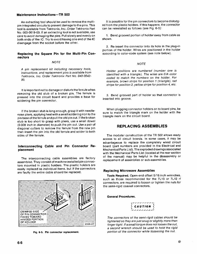
The interconnecting cable assemblies are factory
of the manual) may be helpful in the disassembly or
assembled . They consist of machine installed pin connec-
replacement of assemblies or sub-assemblies .
tors mounted in plastic holders. The plastic holders areeasily replaced as individual items, but if the connectorsare faulty the entire cable should be replaced .
Replacing Microwave Assemblies
CRIMPED SIDEOF PIN CONNECTORFACESTOWARDHINGED PORTION:OFHOLDER
NOTE
Tools Required . Open-end offset 5/16 inch wrenches,such as those recommended for the 7L13 or 7L12 rfconnectors, are required to loosen or tighten the nuts forthe semi-rigid coaxial connectors .
General Procedures .
NOTE
Holder positions are numbered (number one isidentified with a triangle). The wires are EIA colorcoded to match the numbers on the holder. Forexample, brown stripe for position 1 (triangle), redstripe for position 2, yellow stripe for position 4, etc.
3. Bend grooved part of holder so that connector is
inserted into groove .
CAUTION
The connectors of the semi-rigid cables should betightened so they are just snug or slightly more thanfin er ti ht. If a small for ue does not loosen the nut,9 9
qa second wrench should be used to hold the rigid
Fig. 6-5. Pin connector replacement .
portion of the connector while loosening the nut.

1 . Separate the two sections of the instrument asshown in Fig. 6-6.
2. Loosen and remove the semi-rigid coaxial cableconnectors to the applicable assembly, then, if theassembly has soldered connectors and ribbon cableunplug the multi-pin plug at the circuit board .
3. Loosen and remove the mounting screws andremove the assembly .
4. Reverse this procedure to replace the assembly .
Fig.6-6 . Procedure for separating the two sections of 4he7R 502.
Maintenance Instructions-TR 502
Fig. 6-7. Typical position 4or the mixer assembly in the 2.2 GHzfilter assembly .
Replacing the 2.2 GHz Four Cavity Filter Assembly(A320) or the Mixer Assembly (A310)The filter assembly is pretuned at the factory so only
slight adjustments are required after it is installed . Themixer affects filter response, therefore, if either assemblyis replaced, retuning the filter and adjusting the mixercoupling will be required . The orientation of the mixeraffects mixer balance and the suppression of a 2.2 GHzspur . If the mixer is positioned as shown in Fig. 6-7, thespur will usually be down 70 dB or more . If spurs shouldappear, adjust the orientation to minimize .
The following equipment is required to tune thefilter/mixer combination .
1 .
Power Supply with variable output from 0 to 10 V at0 to 40 mA: Tektronix PS 501 of the TM 500-Series .
2. Adapter: BNC female to subminature (SEALEC-TRO}female : Tektronix Part No . 175-1162-00 or SEALEC-TRO Part No . 51-077-6801 .
3. Adapter : BNC male to BNC male : Short length of50 S2 coaxial cable with BNC connectors or an adapter,Tektronix Part Number 103-0028-00.
4. Adapter: N female to BNC male . Tektronix Part No .103-0058-00.
6-7
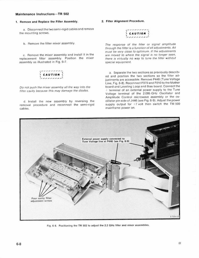
Maintenance Instructions-TR 502
1 . Remove and Replace the Filter Assembly .
2. Filter Alignment Procedure .
a .
Disconnect the two semi-rig id cables and removethe mounting screws .
b . Remove the filter mixer assembly .
c . Remove the mixer assembly and install it in thereplacement filter assembly . Position the mixerassembly as illustrated in Fig . 6-7 .
The response of the filter or signal amplitudethrough the filter is a function of all adjustments . Allmust be very close to optimum . If the adjustmentsare moved to where the signal is no longer seen,there is virtually no way to tune the filter withoutspecial equipment .
C A U T 10 N
a.
Separate the two sections as previously describ-N^
ed and position the two sections so the filter ad-justments are accessible . Remove P446 (Tune VoltageLine, Fig . 6-8) . Reconnect P370 and P210 to the Mother
Do not push the mixer assemby all the way into the
board and Leveling Loop and Bias board . Connect the
filter cavity because this may damage the diodes .
+ terminal of an external power supply to the TuneVoltage terminal of the 2 .095 GHz Oscillator andAmplitude Control microwave assembly or the os
d .
Install
the
new
assembly
by
reversing
the
cillator pin side of J446 (see Fig . 6-9) . Adjust the power
removal procedure and reconnect the semi-rigid
supply output for +7 volt then switch the TM 500
cables .
mainframe power on .
Fig . 6-8 . Positioning the TR 502 to adjust the 2.2 GHz filter and mixer assemblies .

b .
Connect the 2nd LO output of the spectrum
h .
Maximize the filter response signal amplitude byanalyzer to the 2nd LO INPUT of the TR 502.
adjusting the power supply voltage . Do not exceed20 volts.
c . Apply the 50 MHz Calibrator signal to the RFInput of the spectrum analyzer and set the FrequencySpan/Div to 5 MHz with a Resolution of 300 kHz. Usingthe 100 MHz signal as a reference, tune the CenterFrequency to 105 MHz by tuning the 100 MHz signalone division to the left of center . After the analyzercenter frequency has been set to 105 MHz, disconnectthe Calibrator signal to the RF Input .
d . Use a short 50 S2 cable and adapter to connectthe IF Output of the 2 .095 GHz Oscillator andAmplitude Control microwave assembly to the RF I nputof the spectrum analyzer .
e .
Adjust the voltage of the power supply to tune the2.095 GHz oscillator so the 105 MHz IF signal iscentered on screen .
f .
Move the cable from the spectrum analyzer (7L13or 7L12) 2nd LO Out to the 1 st LO Out so the 1 st LO Outsignal is now applied to the TR 502 2nd LO INconnector.
g . Set the spectrum analyzer Frequency Span/Divto 5 MHz, Resolution to 3 MHzand the DisplayMode to2 dB/Div .
Maintenance Instructions-TR 502
i . Loosen the mixer clamp, so the coupling andorientation can be adjusted, then position the mixer asindicated in Fig . 6-7 (apex of the 3 screws up) .
j .
Adjust the four cavities and the mixer coupling forthe best flat-top bandpass response . Keep the responsecentered at the reference frequency as you adjust andbe very careful to not lose the signal . Typical responsesare shown in Fig . 6-10 .
This completes the calibration of the TR 502. Perfor-ming the verification checks in the Performance Checksection to ensure that it meets specifications .
(A) Detuned filter/mixer response .
(B) Good response waveform for filter/mixer assembly.1735-15
Fig . 6-10 . Typical response characteristics of the filter/mixerFig. 6-9. Location of P446 on the Mother board.
assemblies .
ti-9

OPTION INFORMATIONYour instrument may be equipped with one or more options. This section
describes those options, or directs the reader to where the option is documented .
Section 7-TR 502

REPLACEABLEELECTRICAL PARTS
PARTS ORDERING INFORMATION
Replacement parts are available from orthrough your localTektronix, Inc. Field Officeor representative.
Changes to Tektronix instruments are sometimes made to accommodate improvedcomponents as they become available, and to give you the benefit of the latest circuitimprovements developed in our engineering department . It is therefore important, whenordering parts, to include the following information in your order : Part number, instrumenttype or number, serial number, and modification number if applicable .
If a part you have ordered has been replaced with a new or improved part, your localTektronix, Inc . Field Office or representative will contactyou concerning any change in partnumber .
Change information, if any, is located at the rear of this manual .
SPECIAL NOTES AND SYMBOLSX000
Part first added at this serial number
OOX
Part removed after this serial number
ITEM NAME
In the Parts List, an Item Name is separated from the description by a colon ( :) .Because of space limitations, an Item Name may sometimes appear as incomplete . Forfurther Item Name identification, the U .S . Federal Cataloging Handbook H6-t can beutilized where possible .
ABBREVIATIONS
ACTR ACTUATOR
PLSTC PLASTICASSY ASSEMBLY
QTZ QUARTZCAP CAPACITOR
RECP RECEPTACLECER CERAMIC
RES RESISTORCKT
CIRCUIT
RF
RADIO FREQUENCYCOMP COMPOSITION
SEL SELECTEDCONN CONNECTOR
SEMICOND SEMICONDUCTORELCTLT ELECTROLYTIC
SENS SENSITIVEELEC ELECTRICAL
VAR VARIABLEINCAND INCANDESCENT
WW
WIREWOUNDLED
LIGHT EMITTING DIODE
XFMR
TRANSFORMERNONWIR
NON WIREWOUND
XTAL
CRYSTAL

ReplaceableElectricalParts-TR5028-2CROSS INDEX-MFR. CODE NUMBER TO MANUFACTURER
Mfr. Code
Manufacturer
Address
City, State, Zip
01121
ALLEN-BRADLEY COMPANY
1201 2ND STREET SOUTH
, MILWAUKEE, WI 53204
01295
TEXAS INSTRUMENTS, INC.SEMICONDUCTOR GROUP
P.O . BOX 5012
DALLAS, TX 75222
02735
RCA CORPORATION, SOLID STATE DIVISION
ROUTE 202
SOMERVILLE, NY 08876
03508
GENERAL ELECTRIC COMPANY, SEMI-CONDUCTOR
`PRODUCTS DEPARTMENT
ELECTRONICS PARK
SYRACUSE, NY 13201
04222
AVX CERAMICS, DIVISION OF AVX CORP .
POBOX 867
MYRTLE BEACH, SC 29577
04423
TELONIC INDUSTRIES, INC.
21282 LAGUNA CANYON ROAD
LAGUNA BEACH, CA 92652
04713
MOTOROLA, INC., SEMICONDUCTOR PROD . DIV.
5005 E MCDOWELL RD,PO BOX 20923
PHOENIX, AZ 85036
07263
FAIRCHILD SEMICONDUCTOR, A DIV. OFFAIRCHILD CAMERA AND INSTRUMENT CORP.
464 ELLIS STREET
MOUNTAIN VIEW, CA 94042
14433
ITTSEMICONDUCTORS
3301 ELECTRONICS WAYPO BOX 3049
WEST PALM BEACH, FL 33402
15238
ITTSEMICONDUCTORS, A DIVISION OF INTERNATIONAL TELEPHONEANDTELEGRAPH CORP.
P.O. BOX 168, 500 BROADWAY
LAWRENCE, MA 01841
18203
ENGELMANN MICROWAVE CO .
SKYLINE DR .
MONTVILLE, NJ 07045
18324
SIGNETICS CORP .
811 E. ARGUES
SUNNYVALE, CA 94086
21847
AERTECH INDUSTRIES
825 STEWART DR .
SUNNYVALE, CA 94086
27014
NATIONAL SEMICONDUCTOR CORP.
2900 SEMICONDUCTOR DR .
SANTACLARA, CA 95051
32997
BOURNS, INC., TRIMPOT PRODUCTS DIV.
1200 COLUMBIA AVE.
RIVERSIDE, CA 92507
55680
NICHICON/AMERICA/CORP.
6435 N PROESEL AVENUE
CHICAGO, IL 60645
56289
SPRAGUE ELECTRIC CO .
87 MARSHALL ST .
NORTH ADAMS, MA 01247
59660
TUSONIX INC.
2155 N FORBES BLVD
TUCSON, AZ 85705
71034
BLILEY ELECTRIC CO .
2545 W. GRANDVIEW BLVD .
ERIE, PA 16512
72982
ERIE TECHNOLOGICAL PRODUCTS, INC.
644 W. 12TH ST .
ERIE, PA 16512
75042
TRW ELECTRONIC COMPONENTS, IRC FIXEDRESISTORS, PHILADELPHIA DIVISION
401 N. BROAD ST :
PHILADELPHIA, PA 19108
80009
TEKTRONIX, INC.
POBOX 500
BEAVERTON, OR 97077
91637
DALE ELECTRONICS, INC.
P. O. BOX609
COLUMBUS, NE 88601
96733
SAN FERNANDO ELECTRIC MFG CO
1501 FIRST ST
SAN FERNANDO, CA 91341
S0557
TOKYO SHIBAURA ELECTRIC CO ., LTD.
TOKYO, JAPAN
S3774
OSHINO ELECTRIC LAMP WORKS LTD
5 2 MINAMI SHINAGAWA 2 CHORESHINAGAWA KU
TOKYO, JAPAN
S4091
SANYO ELECTRIC CO LTD
OSAKAJAPAN
REV AUG 1984

Replaceable Electrical Parts-TR 502
Tektronix
Serial/Model No .
MfrCkt No .
Part No .
Eff
Dscont
Name & Description
Code
Mfr Part Number
A60
119-0738-00
AMPLIFIER:2 TO 4 GHZ
80009
119-0738-00A70
119-0633-00
ISOLATOR,RF REF:1 .2-4GHZ,20DB MIN
21847
ASI2040A80
015-1027-00
FILTER,LOW PASS:4 .5 GHZ
80009
015-1027-00A90
119-0751-00
FILTER,BANDPASS:INTERDIGITAL
80009 119-0751-00A100
119-0633-00
ISOLATOR,RF REF:1 .2-4GHZ,20DB MIN
21847
ASI2040A110
119-0732-00
MIXER ASSEMBLY:OUT PUT
80009
119-0732-00
A120
119-0736-00
AMPUDETASSY:0.1-1800MHZ
80009
119-0736-00A130
119-0740-00
ATTENUATOR ASSY:2-50 OHM,STEP ATTENUATOR
04423
OBDA140
119-0737-00
AMPTD CONT ASSY:2.095 GHZOSC
80009
119-0737-00A150
670-4145-00
CKT BOARD ASSY:LEVELING LOOP &L BIAS
80009
670-4145-00A310
119-0306-03
MIXER UNIT,BAL :
80009
119-0306-03A320
119-0735-01
FILTER,RFI :LOW PASS FILTER
80009
119-0735-01
A350A1
670-4144-00
B010100
8029999
CKT BOARD ASSY:MOTHER
80009
670-4144-00A350A1
670-4144-01
8030000
8030142
CKT BOARD ASSY:MOTHER
80009
670-4144-01A350A1
670-4144-02
8030143
8031078
CKT BOARD ASSY:MOTHER
80009
670-4144-01A350A1
670-4144-03
8031079
8031079
CKT BOARD ASSY:MOTHER
80009
670-4144-03A350A1
670-4144-04
8031080
CKT BOARD ASSY:MOTHER
80009
670-4144-04A350A2
670-4141-00
8010100
8010339
CKTBOARD ASSY:105 MHZ AMPLIFIER
80009
670-4141-00
A350A2
670-4141-01
B010340
CKT BOARD ASSY:105 MHZAMPLIFIER
80009
670-4141-01A350A3
670-4143-00
CKT BOARD ASSY:52.5 MHZ OSCILLATOR
80009
670-4143-00A350A4
670-4142-00
CKT BOARD ASSY:THETA-FREO DETECTOR
80009
670-4142-00
C150
283-0129-00
CAP.,FXD,CER DI :0 .56UF,20%,100V
56289
3C37X5R564M050B
C162
283-0129-00
CAP.,FXD,CER DI :0.56UF,20%,100V
56289
3C37XSR564M050BC174
283-0129-00
CAP.,FXD,CER DI :0.56UF,20%,100V
56289
3C37X5R564M050BC186
283-0129-00
CAP.,FXD,CER DI :0.56UF,20%,100V
56289
3C37X5R564M050BC202
283-0346-00
CAP.,FXD,CER DI :0.47UF,+80-20%,100V
72982
8131-M100F474ZC210
283-0341-00
CAP.,FXD,CER DI :0.047UF,10%,100V
72982
8121N153X7R0473KC212
283-0346-00
CAP.,FXD,CER DI :0 .47UF,+80-20%,100V
72982
8131-M100F474Z
C218
283-0346-00
CAP.,FXD,CER DI :0 .47UF,+80-20%,100V
72982
8131-M100F474ZC226
283-0346-00
CAP.,FXD,CER DI :0 .47UF,+80-20%,100V
72982
8131-M100F474ZC232
283-0129-00
CAP.,FXD,CER DI :0 .56UF,20%,t00V
56289
3C37X5R564MOSOBC250
290-0340-00
CAP.,FXD,ELCTLT:I0UF,10%,50V
56289 109D106X9050C2C254
283-0346-00
CAP.,FXD,CER DI :0 .47UF,+80-20%,100V
72982
8131-M100F474ZC260
290-0340-00
CAP.,FXD,ELCTLT:I0UF,10%,50V
56289 109D106X9050C2
C262
283-0346-00
CAP.,FXD,CER DI :0 .47UF,+80-20%,100V
72982
8131-M100F474ZC360
283-0197-00
CAP.,FXD,CER DI :470PF,5%,t00V
72982
8121N075COG0471JC362
283-0346-00
CAP.,FXD,CER DI :0 .47UF,+80-20%,100V
72982
8131-M100F474ZC364
281-0752-00
CAP.,FXD,CER DI :0.00175UF,10A
72982
1214-007C366
281-0752-00
CAP.,FXD,CER DI :0.00175UF,10A
72982
1214-007C374
283-0114-00
CAP.,FXD,CER D1 :0.0015UF,5%,200V
59660
805534YSD0152J
C384
290-0513-00 8010100 8031079 CAP.,FXD,ELCTLT:510UF,+75-10%,25V
56289 109D575C384
290-0917-00 8031080
CAP.,FXD,ELCTLT:220UF,+50-10%,25V
55680 TLB1V221TCANNAC386
281-0752-00
CAP.,FXD,CER DI :0.00175UF,10A
72982
1214-007C388
281-0752-00
CAP.,FXD,CER D1 :0 .00175UF,10A
72982
1214-007C390
281-0752-00
CAP.,FXD,CER DI :0 .00175UF,10A
72982
1214-007C404
283-0060-00
CAP.,FXD,CER DI :100PF,5%,200V
59660
855-535U2J101J
C408
283-0346-00
CAP.,FXD,CER DI :0 .47UF,+80-20%,100V
72982
8131-M100F474ZC410
283-0167-00
CAP.,FXD,CER DI :0 .1UF,10%,100V
72982
8131N145X5R0104KC412
283-0346-00
CAP.,FXD,CER DI :0 .47UF,+80-20%,100V
72982
8131-M100F4742C420
281-0752-00
CAP.,FXD,CER DI :0 .00175UF,10A
72982
1214-007C422
281-0752-00
CAP.,FXD,CER DI :0 .00175UF,10A
72982
1214-007C424
285-0882-00
CAP.,FXD,PLSTC:0 .047UF,10%,100V
56289 LP66A1B473K001
REV AUG 1984 8-3

Replaceable Electrical Parts-TR 502
Tektronix
Serial/Model No .
Mfr
Ckt No .
Part No .
Eff
Dscont
Name & Description
Code
Mfr Part Number
C428
285-0882-00
CAP.,FXD,PLSTC:0 .047UF,10%,100V
56289 LP66A1B473K001
C432
283-0346-00
CAP.,FXD,CER DI :0.47UF,+80-20%,100V
72982
8131-M100F474Z
C450
283-0114-00
CAP.,FXD,CER DI :0.0015UF,5%,200V
59660
805534YSD0152J
C452
283-0103-00
CAP.,FXD,CER DI :180PF,5%,500V
59660
831-518-Z500181J
C454
283-0116-00
CAP.,FXD,CER DI :820PF,5%,500V
59660
801547B821J
C456
290-0512-00
CAP.,FXD,ELCTLT :22UF,20%,15V
56289 196D226X0015KA1
C466
283-0196-00
CAP.,FXD,CER DI :270PF,10%,SOV
72982
8101B057X7R0271K
C480
283-0346-00
CAP.,FXD,CER DI :0 .47UF,+80-20%,100V
72982
8131-M100F474Z
C490
283-0346-00
CAP.,FXD,CER DI :0 .47UF,+80-20%,100V
72982
8131-M100F474Z
C494
283-0346-00
CAP.,FXD,CER DI :0 .47UF,+80-20%,100V
72982
8131-M100F474Z
C498
283-0346-00
CAP.,FXD,CER DI :0 .47UF,+80-20%,t00V
72982
8131-M100F474Z
C500
283-0103-00
8010100
8010339
CAP.,FXD,CER DI :180PF,5%,500V
59660
831-518-Z5D0181J
C500
283-0107-00
8010340
CAP.,FXD,CER DI :51PF,5%,200V
96733
R3017
C502
283-0114-00
8010100
8010339
CAP.,FXD,CER DI :0 .0015UF,5%,200V
59660
805534YSD0152J
C502
283-0204-00
8010340
CAP.,FXD,CER D1 :0 .01UF,20%,50V
96733
R2676
C506
283-0103-00
8010100
8010339
CAP.,FXD,CER DI :180PF,5%,500V
59660
831-518-Z5D0181J
C508
283-0103-00
8010100
8010339
CAP.,FXD,CER DI :180PF,5%,500V
59660
831-518-Z5D0181J
C510
283-0067-00
8010340
CAP.,FXD,CER D1 :0 .001UF,10%,20pV
59660
835-515-Z5D0102K
C512
283-0168-00
8010340
CAP.,FXD,CER DI :12PF,5%,100V
72982
8101B121COG0120J
C514
283-0103-00
8010100
8010339
CAP.,FXD,CER DI :180PF,5%,500V
59660
831-518-Z5D0181J
C514
283-0204-00
8010340
CAP.,FXD,CER DI :0.01UF,20%,50V
96733
R2676
C516
283-0346-00
8010100
8010339
CAP.,FXD,CER DI :0.47UF,+80-20%,100V
72982
8131-M100F474Z
C518
283-0103-00
B010100
8010339
CAP.,FXD,CER DI :180PF,5%,500V
59660
831-518-Z5D0181J
C520
283-0067-00
8010340
CAP.,FXD,CER DI :O.OOtUF,10%,200V
59660
835-515-Z5D0102K
C522
283-0346-00
CAP.,FXD,CER DI :0 .47UF,+80-20%,100V
72982
8131-M100F474Z
C523
283-0067-00
8010340
CAP.,FXD,CER DI :0 .001UF,10%,200V
59660
835-515-Z5D0102K
C524
281-0167-00
CAP.,VAR,CER DI :9-45PF,200V
59660
538-011 D9-45
C526
281-0508-00
CAP.,FXD,CER DI :12PF,+/-O.6PF,SOOV
04222
7001-COG-120J
C528
283-0346-00
CAP.,FXD,CER DI :0 .47UF,+80-20%,t00V
72982
8131-M100F474Z
C532
283-0346-00
CAP.,FXD,CER DI :0 .47UF,+80-20%,100V
72982
8131-M100F474Z
C542
283-0239-00
CAP.,FXD,CER DI :0 .022UF,10%,SOV
72982
8121N083X7R0223K
C544
283-0346-00
CAP.,FXD,CER DI :0.47UF,+80-20%,10pV
72982
8131-M100F474Z
C550
283-0346-00
CAP.,FXD,CER DI :0.47UF,+80-20%,100V
72982
8131-M100F474Z
CR212
152-0141-02
SEMICOND DVC,DI:SW,SI,30V,150MA,30V,D0-35
01295
1N4152R
CR214
152-0141-02
SEMICOND DVC,DI:SW,SI,30V,150MA,30V,D0-35
01295
1N4152R
CR216
152-0141-02
SEMICOND DVC,DI:SW,SI,30V,150MA,30V,D0-35
01295
1N4152R
CR250
152-0040-00
SEMICOND DEVICE:SILICON,600V,1A
15238
LG109
CR370
152-0242-00
SEMICOND DVC:SIG,SI,225V,0 .2A,D0-7
07263
FDH5004
CR372
152-0242-00
SEMICOND DVC:SIG,SI,225V,0 .2A,D0-7
07263
FDH5004
CR395
152-0333-00
SEMICOND DVC DI:SW,SI,55V,200MA,D0-35
03508
DJ2011
CR428
152-0574-00
SEMICOND DEVICE:SILICON,120V,0.15A
14433
WG1308
CR456
152-0141-02
SEMICOND DVC,DI:SW,SI,30V,150MA,30V,D0-35
01295
iN4152R
CR466
152-0141-02
SEMICOND DVC,DI:SW,SI,30V,150MA,30V,D0-35
01295
1N4152R
CR480
152-0061-00
SEMICOND DEVICE:SILICON,175V,100MA
07263
FDH2161
CR526
152-0595-00
SEMICOND DEVICE:VVC,SI,12V,120PF
04713
MV 1404
DS10
150-0048-01
LAMP,INCAND:5V,O.O6A,#683,AGED 8 SEL
S3774
OL683AS15 TPL
L250
108-0395-00
COIL,RF:64UH
80009 108-0395-00
L490
108-0537-00
COIL,RF:2000H
80009 108-0537-00
L506
108-0733-00 B010340
COIL,RF:FIXED,113NH
80009 108-0733-00
L520
108-0733-00 8010340
COIL,RF:FIXED,113NH
80009 108-0733-00
L526
108-0707-00
COIL,RF:150NH
80009 108-0707-00
L540
108-0724-00
COIL,RF:12.5NH
80009 108-0724-00
P120
015-1025-01
TERM.,COAX:3MM MALE,50 OHM,W/CH
18203
T186C5
0210
151-0103-00
TRANSISTOR:SILICON,NPN
80009 151-0103-00
8-4REV AUG 1984

Replaceable Electrical Parts-TR 502
Tektronix
Serial/Model No.
Mfr
Ckt No .
Part No.
Eff
Dscont
Name & Description
Code
Mfr Part Number
0390
151-0364-00
TRANSISTOR :SILICON,PNP
80009
151-0364-00
0395
151-0301-00
TRANSISTOR:SILICON,PNP
27014 2N2907A0410
151-0134-00
TRANSISTOR:SILICON,PNP
80009
151-0134-00
0420
151-0286-00 8010100 8031078 TRANSISTOR:SILICON,NPN
S0557 2SC515A
0420
151-0758-00
8031079
TRANSISTOR:NPN,SI,TO 200
S4091
2SC1757 W/350V
0430
151-0508-00
TRANSISTOR:UJT,SI,2N6027,T0-98
03508 X13T520
0440
151-0302-00
TRANSISTOR:SILICON,NPN
07263 5038487
0445
151-0302-00
TRANSISTOR:SILICON,NPN
07263 S038487
0450
151-0302-00
TRANSISTOR:SILICON,NPN
07263 S038487
0455
151-0302-00
TRANSISTOR:SILICON,NPN
07263 S038487
0480
151-0136-00
TRANSISTOR:SILICON,NPN
02735 35495
0500
151-0367-00
8010340
TRANSISTOR:SILICON,NPN,SEL FROM 3571TP
04713
SPS 8811
0505
151-0367-00
8010340
TRANSISTOR:SILICON,NPN,SEL FROM 3571TP
04713
SPS 8811
0510
151-0367-00
8010340
TRANSISTOR:SILICON,NPN,SEL FROM 3571TP
04713
SPS8811
R5
311-0645-00
RES.,VAR,NONWIR:50K OHM,20%,0.50W
01121
GS1N048S503MA
R10
311-1341-00
RES.,VAR,WWaOK OHM,5%,0.25%
01121
534-9608103)
R20
311-1298-00
RES.,VAR,NONWIR:IOK OHM,20%,0.50W
01121
W-7909
R150
321-0167-00
RES.,FXD,FILM:536 OHM,1%,0.125W
91637
MFF1816G536ROF
R152
315-0184-00
RES.,FXD,CMPSN :180K OHM,5%,0.25W
01121
CB1845
R154
315-0103-00
RES.,FXD,CMPSN:IOK OHM,5%,0.25W
01121
C81035
R156
315-0104-00
RES.,FXD,CMPSN:100K OHMS%,0.25W
01121
C81045
R158
315-0272-00
RES.,FXD,CMPSN:2 .7K OHMS%,0.25W
01121
CB2725
R160
321-0193-00
RES.,FXD,FILM:IK OHM,1%,0.125W
01121
ORD BY DESCR
R162
321-0167-00
RES.,FXD,FILM:5360HM,1%,0.125W
91637 MFF1816G536ROF
R164
315-0184-00
RES.,FXD,CMPSN:180K OHMS%,0.25W
01121
CB1845
R166
315-0103-00
RES.,FXD,CMPSNaOK OHMS%,0.25W
01121
CB1035
R168
315-0104-00
RES.,FXD,CMPSNa00K OHMS%,0.25W
01121
CB1045
R170
315-0272-00
RES.,FXD,CMPSN:2 .7K OHM,5%,0.25W
01121
CB2725
R172
321-0193-00
RES.,FXD,FILM :IK OHM,1%,0.125W
01121
ORD BY DESCR
R174
----------
(NOMINAL VALUE,SELECTED)
R176
315-0184-00
RES.,FXD,CMPSN:180K OHMS%,0.25W
01121
CB1845R178
315-0103-00
RES.,FXD,CMPSNaOK OHM,5%,0.25W
01121
CB1035R180
315-0104-00
RES.,FXD,CMPSN:100K OHM,5%,0.25W
01121
CB1045R182
315-0272-00
RES.,FXD,CMPSN:2 .7K OHM,5%,0.25W
01121
CB2725R184
321-0193-00
RES.,FXD,FILM :IK OHM,1%,0.125W
01121
ORD BY DESCR
R188
315-0184-00
RES.,FXD,CMPSN:180K OHM,5%,0.25W
01121
CB1845
R190
315-0103-00
RES.,FXD,CMPSN:IOK OHM,5%,0.25W
01121
CB1035
R192
315-0104-00
RES.,FXD,CMPSN:100K OHMS%,0.25W
01121
CB1045R194
315-0272-00
RES.,FXD,CMPSN:2 .7K OHMS%,0.25W
01121
CB2725
R196
321-0193-00
RES.,FXD,FILMaK OHM,1%,0.125W
01121
ORD BY DESCRR200
315-0101-00
RES.,FXD,CMPSN :100 OHMS%,0.25W
01121
CB1015
R202
321-0422-00
RES.,FXD,FILM:243K OHM,1%,0.125W
91637
MFF1816G24302F
R204
315-0243-00
RES.,FXD,CMPSN:24K OHM,5%,0.25W
01121
CB2435
R206
315-0912-00
RES.,FXD,CMPSN:9 .1K OHM,5%,0.25W
01121
CB9125
R207
315-0472-00
RES.,FXD,CMPSN:4 .7K OHM,5%,0.25W
01121
CB4725
R208
321-0251-00
RES.,FXD,FILM :4 .02K OHM,1%,0.125W
91637
MFF1816G40200FR209
315-0821-00
RES.,FXD,CMPSN:820 OHMS%,0.25W
01121
CB8215R210
321-0222-00
RES.,FXD,FILM :2K OHM,1%,0.125W
91637
MFF1816G20000F
R211
315-0472-00
RES.,FXD,CMPSN:4 .7K OHMS%,0.25W
01121
CB4725R212
315-0683-00
RES.,FXD,CMPSN:68K OHM,5%,0.25W
01121
CB6835R214
321-0228-00
RES.,FXD,FILM :2 .32K OHM,1%,0.125W
91637
MFF1816G23200FR215
311-1268-00
RES.,VAR,NONWIR :IOK OHM,10%,0.50W
32997
3329P-L58-103R218
315-0100-00
RES.,FXD,CMPSN:10 OHMS%,0.25W
01121
CB1005R220
311-1271-00
RES.,VAR,NONWIR :50K OHM,10%,0.50W
32997
3329P-L58-503
REV AUG 1984
8"5
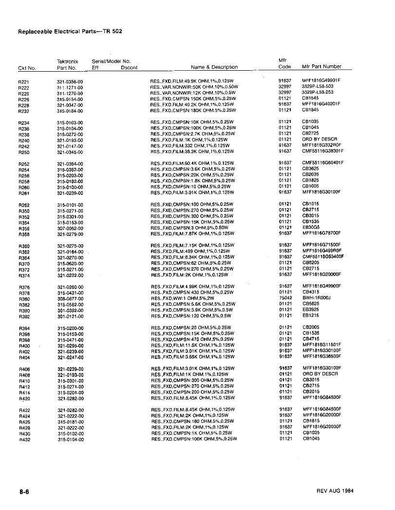
ReplaceableElectricalParts-TR502Tektronix
Serial/Model No .
MfrCkt No .
Part No .
Eff
Dscont
Name & Descriptio n
Code
Mfr Part Number
R221
321-0356-00
RES.,FXD,FILM :49.9K OHM,1%,0.125W
91637
MFF1816G49901F
R222
311-1271-00
RES.,VAR,NONWIR :50K OHM,10%,0.50W
32997
3329P-L58-503R225
311-1270-00
RES.,VAR,NONWIR:I2K OHM,10%,0.5W
32997
3329P-L58-253
R226
315-0154-00
RES.,FXD,CMPSN :150K OHMS%,0.25W
01121
CB1545R228
321-0347-00
RES.,FXD,FILM:40.2K OHM,1%,0.125W
91637
MFF1816G40201F
R232
315-0184-00
RES.,FXD,CMPSN :180K OHMS%,0.25W
01121
CB1845
R234
315-0103-00
RES.,FXD,CMPSN :IOK OHM,5%,0.25W
01121
CB1035R236
315-0104-00
RES.,FXD,CMPSNa00K OHMS%,0.25W
01121
CB1045R238
315-0272-00
RES.,FXD,CMPSN :2 .7K OHM,5%,0.25W
01121
C82725
R240
321-0193-00
RES.,FXD,FILMaK OHM,1%,0.125W
01121
ORD BY DESCR
R242
321-0147-00
RES.,FXD,FILM:332 OHM,1%,0.125W
91637
MFF1816G332ROF
R250
321-0345-00
RES.,FXD,FILM:38.3K OHM,1%,0.125W
91637
CMF55116G38301F
R252
321-0364-00
RES.,FXD,FILM:60.4K OHM,1%,0.125W
91637
CMF55116G60401F
R254
315-0362-00
RES.,FXD,CMPSN:3 .6K OHMS%,0.25W
01121
CB3625R256
315-0203-00
RES.,FXD,CMPSN:20K OHMS%,0.25W
01121
CB2035
R258
315-0182-00
RES.,FXD,CMPSN:I .BK OHM,5%,0.25W
01121
CB1825R260
315-0100-00
RES.,FXD,CMPSN:10 OHMS%,0.25W
01121
CB1005R261
321-0239-00
RES.,FXD,FILM :3 .O1K OHM,1%,0.125W
91637
MFF1816G30100F
R262
315-0101-00
RES.,FXD,CMPSN:100 OHM,5%,0.25W
01121
CB1015R350
315-0271-00
RES.,FXD,CMPSN:270 OHM,5%,0.25W
01121
C82715R352
315-0301-00
RES.,FXD,CMPSN:300 OHM,5%,0.25W
01121
C83015
R354
315-0153-00
RES.,FXD,CMPSN:I5K OHMS%,0.25W
01121
CB1535R356
307-0052-00
RES.,FXD,CMPSN:3 OHM,5%,0.50W
01121
EB30G5
R358
321-0279-00
RES.,FXD,FILM :7 .87K OHM,1%,0.125W
91637
MFF1816G78700F
R360
321-0275-00
RES.,FXD,FILM :7 .i5K OHM,1%,0.125W
91637
MFF1816G71500F
R362
321-0164-00
.
RES.,FXD,FILM:499 OHM,1%,0.125W
91637
MFF1816G499ROF
R364
321-0270-00
RES.,FXD,FILM :6 .34K OHM,1%,0.125W
91637
CMF55116G63400F
R370
315-0620-00
RES.,FXD,CMPSN:62 OHM,5%,0.25W
01121
CB6205
R372
315-0271-00
RES.,FXD,CMPSN :270 OHMS%,0.25W
01121
CB2715R374
321-0222-00
RES.,FXD,FILM:2K OHM,1%,0.125W
91637
MFF1816G20000F
R376
321-0260-00
RES.,FXD,FILM :4 .99K OHM,1%,0.125W
91637
MFF1816G49900FR378
315-0431-00
RES.,FXD,CMPSN :430 OHM,5%,0.25W
01121
CB4315R380
308-0677-00
RES.,FXD,WW :1 OHM,5%,2W
75042
BWH-1R000JR382
315-0562-00
RES.,FXD,CMPSN :5 .6K OHMS%,0.25W
01121
CB5625R390
301-0392-00
RES.,FXD,CMPSN :3 .9K OHM,5%,0.5W
01121
EB3925R392
301-0121-00
RES.,FXD,CMPSN :120 OHM,5%,0.5W
01121
EB1215
R394
315-0200-00
RES.,FXD,CMPSN :20 OHM,5%,0.25W
01121
CB2005
R396
315-0153-00
RES.,FXD,CMPSN :I5K OHMS%,025W
01121
C81535R398
315-0471-00
RES.,FXD,CMPSN :470 OHM,5%,0.25W
01121
CB4715
R400
321-0295-00
RES.,FXD,FILM :11.5K OHM,1%,0.125W
91637
MFF1816G11501FR402
321-0239-00
RES.,FXD,FILM :3.01KOHM,1%,0.125W
91637 MFF1816G30100FR404
321-0247-00
RES.,FXD,FILM :3 .65K OHM,1%,0.125W
91637
MFF1816G36500F
R406
321-0239-00
RES.,FXD,FILM :3 .01K OHM,1%,0.125W
91637
MFF1816G30100F
R408
321-0193-00
RES.,FXD,FILM:IK OHM,1%,0.125W
01121
ORD BY DESCR
R410
315-0301-00
RES.,FXD,CMPSN:300 OHM,5%,0.25W
01121
CB3015
R412
315-0271-00
RES.,FXD,CMPSN:270 OHM,5%,0.25W
01121
CB2715R414
315-0201-00
RES.,FXD,CMPSN:200 OHM,5%,0.25W
01121
CB2015R420
321-0282-00
RES.,FXD,FILM :8 .45K OHM,1%,0.125W
91637
MFF1816G84500F
R422
321-0282-00
RES.,FXD,FILM :8 .45K OHM,1%,0.125W
91637
MFF1816G84500FR424
321-0222-00
RES.,FXD,FILM :2K OHM,1%,0.125W
91637
MFF1816G20000FR426
315-0181-00
RES.,FXD,CMPSN:180 OHMS%,0.25W
01121
CB1615R428
321-0222-00
RES.,FXD,FILM :2K OHM,1%,0.125W
91637
MFF1816G20000FR430 315-0102-00
RES.,FXD,CMPSN:IKOHM,5%,0.25W
01121 CB1025R432
315-0104-00
RES.,FXD,CMPSN:100K OHM,5%,0.25W
01121
CB1045
8-6 REV AUG 1984

Replaceable Electrical Parts-TR 502
Tektronix
Serial/Model No .
MfrCkt No .
Part No .
Eff
Dscont
Name & Description
Code
Mfr Part Number
R434
315-0623-00
RES.,FXD,CMPSN :62K OHMS%,0.25W
01121
CB6235R436
315-0243-00
RES.,FXD,CMPSN :24K OHMS%,0.25W
01121
CB2435R438
315-0434-00
RES.,FXD,CMPSN :430K OHM,5%,0.25W
01121
CB4345R440
315-0471-00
RES.,FXD,CMPSN:470 OHM,5%,0.25W
01121
CB4715R441
315-0150-00
RES.,FXD,CMPSN:15 OHMS%,0.25W
01121
CB1505R442
315-0150-00
RES.,FXD,CMPSN:15 OHM,5%,0.25W
01121
CB1505
R444
315-0104-00
RES.,FXD,CMPSN:100K OHM,5%,0.25W
01121
CB1045R446
315-0203-00
RES.,FXD,CMPSN:20K OHM,5%,0.25W
01121
C82035R448
315-0682-00
RES.,FXD,CMPSN:6.8K OHMS%,0.25W
01121
CB6825R450 315-0102-00
RES.,FXD,CMPSN:IKOHM,S%,0.25W
01121 CB1025R451
315-0470-00
RES.,FXD,CMPSN:47 OHM,5%,0.25W
01121
CB4705R452
315-0302-00
RES.,FXD,CMPSN:3K OHMS%,0.25W
01121
CB3025
R453
315-0822-00
RES.,FXD,CMPSN:8 .2K OHMS%,0.25W
01121
CB8225R454
315-0432-00
RES.,FXD,CMPSN:4 .3K OHM,5%,0.25W
01121
CB4325R456
315-0153-00
RES.,FXD,CMPSN:I5K OHMS%,0.25W
01121
CB1535R458
315-0103-00
RES.,FXD,CMPSN:IOK OHM,5%,0.25W
01121
C81035R462
315-0103-00
RES.,FXD,CMPSN:IOK OHM,5%,0.25W
01121
CB1035R464
315-0103-00
RES.,FXD,CMPSNaOK OHMS%,0.25W
01121
CB1035
R466
315-0202-00
RES.,FXD,CMPSN:2K OHMS%,0.25W
01121
CB2025R470
315-0472-00
RES.,FXD,CMPSN:4 .7K OHM,5%,0.25W
01121
CB4725R472
315-0103-00
RES.,FXD,CMPSN :IOK OHMS%,0.25W
01121
C81035R474
315-0154-00
RES.,FXD,CMPSN :150K OHMS%,0.25W
01121
CB1545R475
311-1272-00
RES.,VAR,NONWIR:100K OHM,10%,O.SOW
32997
3329P-L58-104R476
315-0102-00
RES.,FXD,CMPSN :IK OHM,5%,0.25W
01121
CB1025
R480
315-0150-00
RES.,FXD,CMPSN:15 OHMS%,0.25W
01121
CB1505R482
315-0392-00
RES.,FXD,CMPSN:3 .9K OHMS%,0.25W
01121
CB3925R484
315-0271-00
RES.,FXD,CMPSN:270 OHM,5%,0.25W
01121
CB2715R494
315-0300-00
RES.,FXD,CMPSN:30 OHMS%,0.25W
01121
CB3005R498
315-0300-00
RES.,FXD,CMPSN:30 OHMS%,0.25W
01121
CB30058500
315-0680-00
8010100
B010339
RES.,FXD,CMPSN:68 OHMS%,0.25W
01121
C86805
RS00
315-0101-00
B010340
RES.,FXD,CMPSN:100 OHM,5%,0.25W
01121
CB1015R502
315-0471-00
8010100
8010339
RES.,FXD,CMPSN:470 OHMS%,0.25W
01121
CB4715R502
315-0200-00
B010340
RES.,FXD,CMPSN:20 OHMS%,0.25W
01121
C82005R504
315-0471-00
8010100
8010339
RES.,FXD,CMPSN:470 OHM,5%,0.25W
01121
CB4715R504
315-0432-00
8010340
RES.,FXD,CMPSN:4 .3K OHMS%,0.25W
01121
CB4325R506
315-0471-00
8010100
8010339
RES.,FXD,CMPSN:470 OHMS%,0.25W
01121
CB4715
R506
315-0301-00
8010340
RES.,FXD,CMPSN:300 OHMS%,0.25W
01121
CB3015R508
315-0471-00
8010100
8010339
RES.,FXD,CMPSN:470 OHMS%,0.25W
01121
CB4715R508
315-0302-00
8010340
RES.,FXD,CMPSN :3K OHM,5%,0.25W
01121
CB3025R510
315-0471-00
8010100
8010339
RES.,FXD,CMPSN :470 OHM,5%,0.25W
01121
CB4715R510
315-0301-00
8010340
RES.,FXD,CMPSN :300 OHM,5%,0.25W
01121
CB3015R512
315-0471-00
8010100
8010339
RES.,FXD,CMPSN:470 OHMS%,0.25W
01121
CB4715
R512
315-0432-00
8010340
RES.,FXD,CMPSN:4 .3K OHM,5%,0.25W
01121
CB4325R514
315-0471-00
8010100
8010339
RES.,FXD,CMPSN:470 OHM,5%,0.25W
01121
C84715R514
315-0200-00
8010340
RES.,FXD,CMPSN:20 OHM,5%,0.25W
01121
CB2005R516
315-0100-00
8010100
8010339
RES.,FXD,CMPSN:10 OHMS%,0.25W
01121
CB1005R516
315-0301-00
8010340
RES.,FXD,CMPSN:300 OHMS%,0.25W
01121
C83015R518
315-0471-00
8010100
8010339
RES.,FXD,CMPSN:470 OHM,5%,0.25W
01121
CB4715
R518
315-0302-00
B010340
RES.,FXD,CMPSN:3K OHM,5%,0.25W
01121
CB3025R520 315-0102-00
RES.,FXD,CMPSNaKOHM,5%,0.25W
01121 CB1025R521
317-0510-00
8010100
8010339
RES.,FXD,CMPSN:51 OHMS%,0.125W
01121
885105R521
315-0201-00
8010340
RES.,FXD,CMPSN:200 OHMS%,0.25W
01121
CB2015R522
315-0102-00
RES.,FXD,CMPSN:1 K OHMS%,0.25W
01121
CB1025
REV AUG 1984 8-7

Replaceable Electrical Parts-TR 502
Tektronix
Serial/Model No .
Mfr
Ckt No .
Part No .
Eff
Dscont
Name & Description
Code
Mfr Part Number
R523
317-0510-00
8010100
8010339
RES.,FXD,CMPSN :51 OHM,5%,0.125W
01121
885105
R523
315-0621-00 8010340
RES.,FXD,CMPSN:6200HM,5I,0.25W
01121 C86215
R524
315-0301-00
B010340
RES.,FXD,CMPSN:300 OHM,5%,0.25yU
01121
CB3015
R526
315-0200-00
RES.,FXD,CMPSN:20 OHMS%,0.25W
01121
CB2005
R532 315-0100-00
RES.,FXD,CMPSN:100HM,5I,0.25W
01121 CB1005
R536
315-0471-00
RES.,FXD,CMPSN:470 OHM,5%,0.25W
01121
CB4715
R538
315-0471-00
RES.,FXD,CMPSN :470 OHM,5%,0.25W
01121
CB4715
R539
315-0510-00
RES.,FXD,CMPSN :51 OHM,5%,0.25W
01121
C85105
R542
315-0100-00
RES.,FXD,CMPSN:10 OHM,5%,0.25W
01121
CB1005
R544
315-0511-00
RES.,FXD,CMPSN:510 OHMS%,0.25W
01121
C85115
R546
321-0097-00
RES.,FXD,FILM:100 OHM,1%,0.125W
91637
MFF1816G100ROF
R548
321-0097-00
RES.,FXD,FILM:100 OHM,1%,0.125W
91637
MFF1816G100ROF
R549 315-0511-00
RES.,FXD,CMPSN:S100HM,5I,0.25W
01121 C85115
R550
315-0271-00
RES.,FXD,CMPSN :270 OHM,5%,0.25VN
01121
CB2715
R552
315-0471-00
RES.,FXD,CMPSN :470 OHM,5%,0.25W
01121
CB4715
R554
315-0471-00
RES.,FXD,CMPSN:470 OHM,5%,0.25W
01121
CB4715
R556 315-0471-00
RES.,FXD,CMPSN:4700HM,5I,0.25W
01121 C84715
R558
315-0471-00
RES.,FXD,CMPSN:470 OHMS%,0.25W
01121
CB4715
R559
315-0471-00
RES.,FXD,CMPSN:470 OHM,5%,0.25W
01121
CB4715
T520
120-0487-00
8010340
XFMR,TOROID:5 TURNS BIFILAR
80009
120-0487-00
0150
156-0067-00
MICROCIRCUIT,LI:OPERATIONALAMPLIFIER
01295 MICROA741CP
U160
156-0067-00
MICROCIRCUIT,LI:OPERATIONAL AMPLIFIER
01295
MICROA741CP
U170
156-0067-00
MICROCIRCUIT,LI:OPERATIONAL AMPLIFIER
01295
MICROA741CP
U180
156-0067-00
MICROCIRCUIT,LI:OPERATIONAL AMPLIFIER
01295
MICROA741CP
U200
156-0067-00
MICROCIRCUIT,LI :OPERATIONAL AMPLIFIER
01295
MICROA741CP
U240
156-0067-00
MICROCIRCUIT,LI :OPERATIONALAMPLIFIER
01295 MICROA741CP
U250
156-0067-00
MICROCIRCUIT,LI:OPERATIONAL AMPLIFIER
01295
MICROA741CP
U350
156-0053-00
MICROCIRCUIT,LI:VOLTAGE REGULATOR
07263
SL21721
0365
156-0158-00
MICROCIRCUIT,LI:DUAL OPERATIONAL AMPLIFIER
18324
MC1458N
U370
156-0053-00
MICROCIRCUIT,LI:VOLTAGE REGULATOR
07263
SL21721
U390
156-0071-00
MICROCIRCUIT,LI:VOLTAGE REGULATOR
04713
MC1723CL
U450
156-0058-00
REPLACED BY 156:0058-02
U455
156-0172-00
REPLACED BY:156-0172-02
0460
156-0047-00
REPLACED BY 156:0047-02
U470
156-0096-00
MICROCIRCUIT,LI:VOLTAGE COMPARATOR
27014
LM311H
U500
156-0369-00
8010100
8010339
MICROCIRCUIT,DI:TRIPLE LINE RECEIVER
80009
156-0369-00
U520
156-0308-00
MICROCIRCUIT,DI:QUAD DIFF LINE RECEIVER
04713
SC22689P115
U540
156-0369-00
MICROCIRCUIT,DI:TRIPLE LINE RECEIVER
80009
156-0369-00
U545
156-0518-00
MICROCIRCUIT,DI:PHASE-FREQ DETECTOR
04713
MC12040L
U550
156-0230-00
MICROCIRCUIT,DI:DUAL D MA-SLAVE FLIP-FLOP
04713
MC10131 (L OR P)
VR250
152-0127-00
SEMICOND DEVICE:ZENER,0 .4W,7.5V,5%
04713
SZG35009K2
VR258
152-0461-00
SEMICOND DEVICE:ZENER,0 .4W,6.2V,5%,
04713
SZG25002K2
VR262
152-0461-00
SEMICOND DEVICE:ZENER,0.4W,6.2V,5%
04713
SZG25002K2
VR362
152-0461-00
SEMICOND DEVICE:ZENER,0.4W,6.2V,5%
04713
SZG25002K2
VR364
152-0461-00
SEMICOND DEVICE:ZENER,0 .4W,6.2V,5%
04713
SZG25002K2
VR480
152-0304-00
SEMICOND DEVICE:ZENER,0 .4W,20V,5%
15238
25411
W10
175-1746-00
CA ASSY,SP,ELEC :IF OUT
80009
175-1746-00
yk75
175-1720-00
CA ASSY,SP,ELEC:LOWPASS TO ISOLATOR
80009
175-1720-00
W85
175-1713-00
CA ASSY,SP,ELEC:INTERDIGITAL TO 4.5 GHZ
80009
175-1713-00
W95
175-1716-00
CAASSY,SP,ELEC:2 .1-3 .9 TO ISOLATOR
80009
175-1716-00
W105
175-1721-00
CAASSY,SP,ELEC:MIXER TO ISOLATOR
80009
175-1721-00
W130
175-1710-00
CAASSY,SP,ELEC:ATTENUATOR TO RF OUT
80009
175-1710-00
W135
175-1715-00
CAASSY,SP,ELEC :1 DB TO 10 DB
80009
175-1715-00
Y526
158-0098-00
XTAL UNIT,OTZ :52.5 MHZ AT 25 DEG SER RES
71034
K-3105-1
8-8REV AUG 1984

DIAGRAMS AND CIRCUIT BOARD ILLUSTRATIONSSymbols and Reference Designators
Graphic symbols for electrical and logic symbols, used on the diagrams, are based on ANSI Y32 .2, 1970, and ANSI
Y32 .14, 1973, "American National Standards Institute ." Logic symbols depict the logic function of the device in positivelogic . Copies of these standards can be obtained from the Institute of Electrical and Electronics Engineers, 345 East 47thStreet, New York, N.Y ., 11017. Exceptions and additions are shownon this sample diagram . Theseconform or are based onthe manufacturers data sheet and industry trends .
Resistor values are in ohms, unless noted otherwise, and the S2 symbol is omitted . Capacitor values >1 (e.g . 10) are inpicofarads (pF) and values <1 (e .g . 0.01) are in microfarads unless otherwise noted.
R~243oK-
}SV
REV. A MAY 1978
P~ O SWEEP BOARD A100
I
SWEEP AMPLIF~ER~
See Note on Diagram
aoo~- U435/iO
'
Internal Adjustmentowc~
Index on Plug to Circuit Board
R1o_
1OK-
2OK
~
~3
I
Line NameR12~
~ISV~--~ }_50
3
UIO4A
~~I~~ PO`~~T10K '1--Front Panel Control or Adjustment
tMo63vE~TICALOUTZ -
R3"2_OO "E'-- Destination Diagram No
V
4
Soldered, Interconnecting Board Lead�_Ulo
IC Type
IC With Open Collector
Section 9-TR 502
IC Type, Voltage & Pin Out Data
Test Voltage
Coaxial Connector
Refers to Waveform Adjacent toDiagram
Modified Component (see EPL)
Shield
Decoupled or Filtered Voltage
Part of Board - Name & Assembly No
Circuit Board Outline
Diagram Name & Number
RI Oro~-
1735-21

ITRACKGENLOGIC
I~-
I I
4,6 GHz
2.1-5.9 GHz2-4 GNZ
LOW PASS
BANDPA55
2-4 GNz2.1-3.9GHz ISOLATOR FILTER FILTER ISOLATORAMPLIFIER
sINO
alOdOm
a1SdBm
I
I
~
I
--~- '~~.1,
u
I
v
I
II
L-2.2GHz FOUR CAVITY FILTER ASS`Y-
I
2~O
HzOSG
S-12V
I
^
~
I _V
L AMPI\TUDE JCONTROL A55'Y
-98dBm @LOS MHz
v ~
v~ I
I
x
OPERATIONALLOGIC
I
LOCK LOOP
\\COMPENSATIONAMPLIFIER
-----------HONEYCOM
FILTER I
I ~ I____~_ I INORMALIZING I
I
I AMPLIFIERS
~9d61 I " 9GHs I
ILOW PASS
ILo
I FILTER IOUTPU
'VT1F
I ~ i n,
j
IMIXER -90d6m
IRF-29dBm
~
~ I- - - --
d6
I
AMPA1F10ER I
----T-GIAS BIAS C
I LEVELING IATTENUATOR
I
~
I I1 2.2GHzLOW PA95
I
I ATTEN IUATOR 1
I
SdBm
~I LO_W PASS
~ 20dB ~ BANDPASS IH@ I
'
M\XER
2095(olf~odBm ~ DIRECTION AI2u~0 2200M
rILTER I
I FILTER I
I
LOS@-38dBm --"
I
GOUPLCR
I
~-LEVELING LOOP
PHASE/FREQUENCYDETECTORA3S0A4
LOS MHzAMPLIFIERA3SOA2
SIGNALLEVELNORMA'
POWERREGUL
VOLTAGE CONTROLLECRYSTAL OBCILLATOItS2 .SMHZ.)
A3S0A~!

/
/-AMPLIFIER/DETEOTOR ASSIY -
/- - -
/I
I
I
I
i
I
LBGHZ
I PWR IIVDRID~
~
10 d9
/
I dB
/SLOW PASS ;
I
I
I
I
FILTER
I
I
STEP ATTEN
STEP ATTENLOw PASSI FILTER
I
I_ I I I
Od6m
I
I
I
I
I
I
Iu mI
I
;
I
I
I
I
u-- --_-------------
- ATTENUATOR-
BIAS BIAS BIAS BIAS 61AS
~1zFIER~2
ENCYTOR~4
VOLTAGE CONTROLLEDCRYSTAL OSCILLATORlS2,SMNZ.) A3SOA3
SIGNALLEVELNORMALIZATION
POWER SUPPLYREGULATORS
S.1 VfISV
~~-ISV
__--__---_-1
_-_-__-__-u
- - LEVELING LOOP ~ BIAS CKT BRD----
-4 dBm
BLOCK DIAGRAM lO
OUTPUT/------!' .--------LEVEL-darn
/
/
VAR dB
TRACkADJUST
AU% KvOUT
OdBm RF OUT

IoT LOIN
T8502
J
WNNQJOmFOJWOJrJaa
_,y_
OQJJ
UUIO
dIO
SOfON
a
2,2 GHzLOW-PASSFI LTER
NORMALIZINGATTEIJUATOR
-1 .7 VAB
FROM LEV ELIIUG ~ I OSC
iLOOP ~ BIAS BRD
TUNE VOLTAGE
,. .AA
+8V
I r~ ~ ~ r~s r~r
I
IIII
0dB _ _ _ ___ _
_
___ _
I_
ISOLATION
-----
_
----_ +9 .5ALAPLIFIEP
~~ ~ ~-T---
AF
S L
f
~~~
^,
COLLECTOR
-___-____-___
_________~_---IAD
LEVELIAJG
LEVEIINGATTENUATOR
I ATTENUATOR
2.095 GNzOSCILLATOR
-23 dBm
(
AMPLITUDECONTROLLEDOUTPUT
X
-38dBm euLOS MFiz
WIO
RF INPUTZ= SOIL
1F OUTPUT
TO A350LOS MHz AMPLIFIER
d
______~i_________~__________
LB GHs3dB I
LOW-PASS FILTERIIII
I
P200-7
GND SENSE p200_6
-LIoVACe- UORMALIZING
ATTENUATOR
LO OUTPUTlF INPUT
1'735 -23
QEV A JUN 1979
A120 o.l-IBOO~
PZOO
OZO
A310ASSEMBLY A32O 2 .ZOHz F01
~II
I
BANDPASS f

AIZO
0.1-ISOOAAHZ AMPLIFIER/DETECTOR ASSEMBLY
LB GHZ
I
w10E9A1JD I
WvDESA1JD I WIDE~AND I WIDEDAND
i
1.8GHzOW-PASS FILTER
I AMPLIFIER I AMPLIF1ER I AMPLIFIER I AMPLIFIER I LOW-PASSI
I
I
I
I FILTERI
I
I
II
P200
A3ZO 2.20Nz FOUR CAVITY FILTER ASSEMHLV
11I~
s1~
P190
N
d bW J0
of
of
N a0
0
~ ar-
r
r
wW
. >
V >
N >
W >
M>
W >
d ~
N> Nrn
W A
jJl
W m
JS
W ap
JJ:
W CI
JWJ>O
to y
J N
n O
JN
N O
Jm
~_
J~Jf
m +
O +
m +
U+
~ r
~ +
~ +
Ur ~ +
PICOO
AUXOUT
e
iil
MICROWAVE CIRCUITRY
W19S
-4 d8m
,= ?!?D
Aux RFY""~oUT

ZO_F4U iyOJF- QZw C7Z Q
a O
O OU w
TR502
P210n + 15V
L250
U250
P160
R258
_~~wR152
8150
GND A B C D
R164
A150
Leveling Loop & Bias Ckt Brd
0174
U170
R180Y--
R166
R178r--
R202
R20G
C202
8204
~~ C226
1735-16
R171

U160
R168
8180
R192r--
8166
R178 ~_M~190 P170
A150
Leveling Loop & Bias Ckt Brd
1735-16
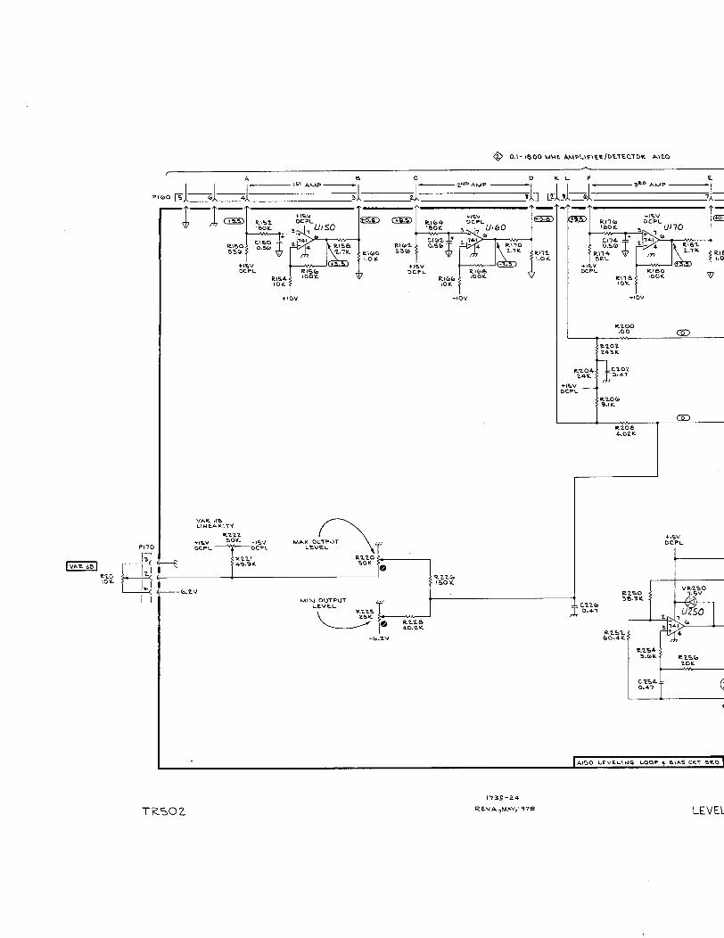
VAR dB
VAR dBLINEARITY
RI50 0.50590
8222+ISV SOK _ISV
PI70 ~
DCPL -~-DCPL
TR50Z
O.I-1800 MN2 AMPL1f1ERIDETECTOR A120
A
B
O
D
K L
FI5T A1.AP
3
2
2uoAMP
'
2
~
0
3RD AMP
+ISV
~
+ISV
+ISV®
~
R104
DCPL
~
+,R
DCPLIBOKUI7OIBOK UISO
I80K UNDO3 7
9 7
3 7t
+ 0
++ 741
uio21+ 741
. . . L+2_
2RISE
I
RI(p2
0.50
Rn0
I
O~SlO
2741
RI824
2
531
4
21Kl
~
_4
~27~.,K
8100 0 .$RI72
8114I'
RI B~LOK
~LOK SEL
\®LO
+
+3.
3.+ISV
+ISV
+ISV
+9. ~ RIS2
DCPL
DCPL 8150
DCPL R10B
DCPL 8180Rloly
TOOK
1
RO6
TOOK
~
RaK~
IOOK
t10V
MAX OUTPUTLEVEL
+1 OV
173$-24
REVA~!v1AY I197B
8200100v.M-
R202243K
8204 1C20224K '7'0.47
+IS~7
VDCPL
82009.1K
82084.02K
+1 OV
+ISvDCPL
$R221
R220i~
jI?49.9K
SOK
R20 Ir
OIDK
I I IR220ISOK
i-0.2V
VR2S08250 'LSV
MIN OUTPUT
98 "3KLEVEL
-I- C220R22S
0"47
U~O2SK
2 _R22B
040.2K
3 '141R2S2 4
-0.2V
00.4K
C 2S40.41
R2S49.(nK R2S0
20K
AISO LEVEl1\.IG LOOP ~ BIAS CKT BRO
LEVEL

DETECTOR A120
3RD AMP
+ISV7(p °CPL ~ +B 8188 DCPL
+o+ISV
OK .~ (/I7~ 180K y- U 18O DCPL+ l l02 ,41
a 1
k°6K
-
_ ..
a¬~i
v
_
v
R2p0100
kD2'~ K
`0202f~ 0 .47
82084.02 K
R2S43,loK
C2S40.41
+ISVDCPL
+lov
a iov
R21IC210
4.lKO.OS
+ISV DCPL
8212
C212~2~~ QZ/~
(e8K 0.412 -,
-1 .5,41 ~°
~ 82103+ 4 W
8201
2.OK4.7 K
u25o_ ,l41 G
jI 3
+IOV
O "4Ki
4
' R2S81 .8K
R2Slo20K
E
H
4TH AAAP
J
`G
4~
5~ 3~~P190
RI84LOK
JEL161G LOOP ~ elAS CKT BRD
®VR2S8la"2V
-ISV 8208DCPL 820
C218 ~-0 .41
+ISVDCPL
-ISV
R242- DCPL
8232
'~92
'
i8218 180K10
+9 . En AF
Oslo T
+ISVDCPL UL ~O
'Y+
2 7417 (°
®--~ f~-AE- 4
8238Z.7K 8240
I,OkR23fo
E'-5 AB8234 TOOKIOK ~
~ ~
AA
P210
+1 OV
L2S0(a4p .H
0250 ~
~ CR25010/~F
VR2SO
-ISV8250 I .SV
DGPL38 .3K
C2102-j- 100 ~R21o20~ 4l
lo,2V
LEVELItJG LOOP C AMPLIFIER BIAS CIRCUITRY
E2ln 1s.ol K
002(00 ~' R2O OH I+
AD
P310~
PIO A3SOA1 MOTHER 6RD-
~-TUtJE VOLTAGEII~ IO50
~ j--+15V4 1 I
ZONQU
a
OJH
Q
Zw
C7
Z
Q
a
~
O
O
U
TR502
P370
OOM
P446
aMU
an
C360
U35C
U370
M

8453
0450
C420G38f:
C490 L49U-lYYI-
Q455
R464
U460
A350A7
1Vlother Board
C364
C390
0422
Q480
+33 .5V R480
8434v
8436
R432
P360
P330
P350

A350A2 105 MHz Amplifier (SN 8010340 & UP)
A350A3 52.5 MHz Oscillator
A350A4
~/f Detector
1735-26
1735-19
1735-20
TR502

P3g0
2.1-3 .9Gi~s ~~ E-+ISVIAMPLIFIER
U
-3DdBmIOS MH2
IDS MHzFROMDIR CPLR
OWERON
TR502
WID ~JD(oO
' R4O1 - +S .IV
DSIO
DI4I
START COUIJTglg
~- +ISVI
gISB10
R500100
YA
e4
~ In
~ sA3 A9
=S] D9
A12 612 g7
A6
A,
A=62-A1=A'11 ehhvl
R'352~33.SV
300
R35fo
Rfn2
430
+ 't0' FO O
9.08350
V
270 RISK4U3SO
CR370 R3(pK+ISVfp
"' 10
~R494
+SD.SV
6 10 "' 2 1
~,
m
,
v0tt
cs 1
30
7 vc v, cL
ILIV cs U3~0c
RSSB+ ~
8V+723HC
INV27.D7K
C494R20CR372gV ,2SHC
V - VR
611 COMP
~0.41
VR IJI V- COMP
5 6
3 9 ~ ~RSfoO
~ R9743 S~ 91C37q
C38ro7.ISK
+7.5
Z.OOK
~ISOO
I,S6'.2v
~6-2V ~
®
C3fo047O
R3,'oU3lo5 R9(o4
4.89K34K
2
11.1SSS8V + ~
~.
0.
-ISV
.499 T
_s
R450IK
~S.I V
Rok9 U450D
1
0450E-~til
L +~ 91 11 1q IV
VC3fofn
C52gee 10115ccl8592
1750,
` I
0.47 T
Vcc2 16 ~C532 10rT7 8110,12 0520
0.4,
CS22
Y52fo0.47 'x'~CZ
S2.5MHn
R51420R502 C502
OI2o
Coiq
T52o
(~-~
R521 L520200 ; 113nH
R516R506 1.506 431K
30o
Q510R504
20
I13nHG500 4.3K
QSOS
00CSZ ~R316~
c
R5230523
}~-t~-'~
.ool
R520 Gooi
620
R 3KH R510 0510
300300 '001
/A9~pA2 105 ~N
AMP IFIEKn
Q45S Ra538.2K
P3~o I
+s.lvl
1c
2
1
U460CR4fo2~
12IOK
+S.IVIA18
GATE 13a5 .1 V1
Rar~a U450C
U460AIOKCOUNTER MODE
13 IZ
S6
Bll
L
R880f "O PS84
~~-(E
C3881750
"
0C3~o~'.R520'I
05208 RS99 I NI,SO
""9025"
TCRSZ~n
7 +
S
51
K FiMODEADJUST
y USZOA !o -RS3g +~~
Rszm
+ 2 ~
a,o2o
LS2~e
4 -
RS31aCS24
ISOnH
q,09-45 CS2fo
12
A350A3 52 5MH2 OSCILIATORI
+5.I 1VI
+Sdv1
R454 ;
R45fn ~ CpSlo4.3K
6204
15K
22NF
,4129 A ~
-14123+ISV I~
g 10
Q4'SO
ClR
OLR A
8
3
SWEEP STOP MODE ENA6LE
11
9
R452SK
1735-25REV NOV 1993
+S.IVI U455A
+°-CR4S~cIm I 14
~ 6 U455B13 Q
D 2
12 Q
03901750
PS10
IE~I 1
u ~-PSSO
U450AU460B
llo
3 4
+5.1V1
C4S0
9
STOP OWEEP
ISOO
D
l5ofIZ .or
OS420.021
85544l0
A350A1 Mo

N'~f'f
04558
14608
STOP SWEEP
L490200,uF
+5.1 VIC4900 . 4T
04508
A350A1 MOTHER 6RD
8390{ ~R'j92iS .IV
8.9K 120
A3SOA4 (QlS DETECTOR
R46~o2KJvJr
+ Ili 0450
'die 0460
C466 i210
R462,aoa
Halo
a .91Lj ry, Qg807,9,11 7
+20VVR4H20V
S .IVI
CRa(o(o
R4,04 ., K
A8 B6
Q390 Rio
a
RS9B RISK4,0Q395
+j9 .SV1
R480I CR460~Sw~-~--~-~~
+93 .SV
1C4B00 .41 ~, \
8464z,o
--vsv8498so
LC4960.4'I
R472 8414IOK 1SOK
-ISVI
+ISVI SWCEPTRfGGERlEV E4
OPERATIONAL LOCK LOGIC, VOLTAGE REGULATOR ~
0PHASE LOCK CIRCUITRY
flAOflR4,5
0~ 1 OOK
ISVI
-ISV 1HSV I
0470LMS11
' P350R4T0
I,K
SWEEP
I ~-~V
L AXIS
SWEEP STOP
NOW SWEEP LOGICPHASE LOCK LOGIC
~ ~S
P210LEVEl1uG100 P f,91AS SRD
TRACKGCuLOGIC

°~ oof
zmo,~amaMVM00JOFm2ZW _fn
~Nd~W
va
A350A2 105 MHz Amplifier (SN 8010339 & BELOW)
,)
Digitally signed byhttp://www.aa4df.com
1735-18

L
m
e
_
- - ~

PARTS ORDERING INFORMATION
INDENTATION SYSTEM
Replacement parts are available from or through your localTektronix, Inc. Field Office or representative .
If a part you have ordered has been replaced with a new or
Parts of Detail Partimproved
part,
your
local Tektronix,
Inc.
Field Office or
Attaching parts for Parts of Detail Partrepresentative will contact you concerning any change in part
_ - -
_ _ _number .
FIGURE AND INDEX NUMBERS
REPLACEABLEMECHANICAL PARTS
ABBREVIATIONS
ITEM NAME
Section 10-TR 502
This mechanical parts list is indented to indicate itemrelationships. Following is an example of the indentation systemused in the description column .
Changes to Tektronix instruments are sometimes made to
f 2 3 4 5
Name 8 Descriptionaccommodate improved components as they become available,and to give you the benefit of the latest circuit improvements
Assembly and/or Componentdeveloped
in our engineering department .
It is therefore
Attaching parts for Assembly and/or Componentimportant, when ordering parts, to include the following
- - -
- - -information in your order: Part number, instrument type or
Detail Part of Assembly and/or Componentnumber, serial number, and modification number if applicable .
Attaching parts for Detail Part
Change information, if any, is located at the rear of this
Attaching Parts always appear in the same indentation asmanual .
the item it mounts, whilethe detail parts are indented to the right .Indented items are part of, and included with, the next higher
SPECIAL NOTES AND SYMBOLS
indentation . The separation symbol---'---indicates the end ofattaching parts.
X000
Part first added at this serial number
OOX
Part removed after this serial number
Attaching parts must be purchased separately, unless otherwisespecified.
Items in this section are referenced by figure and indexnumbers to the illustrations .
in the Parts List, an Item Name is separated from thedescription by a colon (:) . Because of space limitations, an ItemName may sometimes appear as incomplete . For further ItemName identification, the U.S . Federal Cataloging Handbook H6-1cart be utilized where possible .
"
INCH
ELCTRN
ELECTRON
IN
INCH
SE
SINGLE END#
NUMBER SIZE
ELEC
ELECTRICAL
INCAND
INCANDESCENT
SECT
SECTIONACTR
ACTUATOR
ELCTLT
ELECTROLYTIC
INSUL
INSULATOR
SEMICOND SEMICONDUCTORADPTR ADAPTER
ELEM ELEMENT
INTL INTERNAL SHLD SHIELDALIGN
ALIGNMENT
EPL
ELECTRICAL PARTS LIST
LPHLDR
LAMPHOLDER
SHLDR
SHOULDEREDAL ALUMINUM
EOPT EQUIPMENT
MACH MACHINE
SKT SOCKETASSEM ASSEMBLED
EXT EXTERNAL
MECH MECHANICAL
SL SLIDEASSY
ASSEMBLY
FIL
FILLISTER HEAD
MTG
MOUNTING
SLFLKG
SELF-LOCKINGATTEN ATTENUATOR
FLEX FLEXIBLE
NIP NIPPLE
SLVG SLEEVINGAWG
AMERICAN WIRE GAGE
FLH
FLAT HEAD
NON WIRE NOT WIRE WOUND
SPR
SPRINGBD
BOARD
FLTR
FILTER
OBD
ORDER BV DESCRIPTION
SO
SQUAREBRKT
BRACKET
FR
FRAME or FRONT
OD
OUTSIDE DIAMETER
SST
STAINLESS STEELBRS
BRASS
FSTNR
FASTENER
OVH
OVAL HEAD
STL
STEELBRZ
BRONZE
FT
FOOT
PH BRZ
PHOSPHOR BRONZE
SW
SWITCHBSHG
BUSHING
FXD
FIXED
PL
PLAIN or PLATE
T
TUBECAB CABINET
GSKT GASKET
PLSTC PLASTIC
TERM TERMINALCAP
CAPACITOR
HDL
HANDLE
PN ,
PART NUMBER
THD
THREADCER
CERAMIC
HEX
HEXAGON
PNH
PAN HEAD
THK
THICKCHAS
CHASSIS
HEX HD
HEXAGONAL HEAD
PWR
POWER
TNSN
TENSIONCKT
CIRCUIT
HEX SOC
HEXAGONAL SOCKET
RCPT
RECEPTACLE
TPG
TAPPINGCOMP
COMPOSITION
HLCPS
HELICAL COMPRESSION
RES
RESISTOR
TRH
TRUSS HEADCONN
CONNECTOR
HLEXT
HELICAL EXTENSION
RGD
RIGID
V
VOLTAGECOV
COVER
HV
HIGH VOLTAGE
RLF
RELIEF
VAR
VARIABLECPLG
COUPLING
IC
INTEGRATED CIRCUIT
RTNR
RETAINER
W/
WITHCRT
CATHODE RAY TUBE
ID
INSIDE DIAMETER
SCH
SOCKET HEAD
WSHR
WASHERDEG DEGREE
(DENT IDENTIFICATION
SCOPE OSCILLOSCOPE
XFMR TRANSFORMEROWR DRAWER
IMPLR IMPELLER
SCR SCREW
XSTR TRANSISTOR

Replaceable Mechanical Parts-TR 502
CROSS INDEX-MFR. CODE NUMBER TO MANUFACTURER
Mfr . Code
Manufacturer
Address
City, State, Zip
OOOAH
STANDARD PRESSED STEEL CO ., UNBRAKO DIV . 8535 DICE ROAD
SANTA FE SPRINGS, CA 90670OOOCY
NORTHWEST FASTENER SALES, INC .
7923 SW CIRRUS DRIVE
BEAVERTON, OR 97005OOOFH
LEMOSA INC .
465 CALIFORNIA STREET
SAN FRANCISCO, CA 9410400779
AMP, INC.
P 0 BOX 3608
HARRISBURG, PA 1710508261
SPECTRA-STRIP CORP .
7100 LAMPSON AVE .
GARDEN GROVE, CA 9264212327
FREEWAY CORPORATION
9301 ALLEN DRIVE
CLEVELAND, OH 44125
18203
ENGELMANN MICROWAVE CO .
SKYLINE DR .
MONTVILLE, NJ 0704522526
BERG ELECTRONICS, INC .
YOUK EXPRESSWAY
NEW CUMBERLAND, PA 17070
24931
SPECIALITY CONNECTOR CO ., INC .
2620 ENDRESS PLACE
GREENWOOD, IN 4614245722
USM CORP ., PARKER-KALON FASTENER DIV .
CAMPBELLSVILLE, KY 4271870485
ATLANTIC INDIA RUBBER WORKS, INC .
571 W. POLK ST .
CHICAGO, IL 6060771785
TRW, CINCH CONNECTORS
1501 MORSE AVENUE
ELK GROVE VILLAGE, IL 6000773743
FISCHER SPECIAL MFG . CO .
446 MORGAN ST .
CINCINNATI, OH 4520673803
TEXAS INSTRUMENTS, INC ., METALLURGICALMATERIALS DIV.
34 FOREST STREET
ATTLEBORO, MA 0270375497
LAMSON AND SESSIONS CO .
5000 TIEDEMAN ROAD
CLEVELAND, OH 4414478189
ILLINOIS TOOL WORKS, INC .SHAKEPROOF DIVISION
ST . CHARLES ROAD
ELGIN, IL 6012079807
WROUGHT WASHER MFG . CO .
2100 S . 0 BAY ST .
MILWAUKEE, WI 5320780009
TEKTRONIX, INC .
P 0 BOX 500
BEAVERTON, OR 9707783309
ELECTRICAL SPECIALITY CO ., SUBSIDIARY OFBELDEN CORP .
213 E . HARRIS AVE . SOUTH
SAN FRANCISCO, CA 9408083385
CENTRAL SCREW CO .
2530 CRESCENT DR .
BROADVIEW, IL 6015387308
N. L . INDUSTRIES, INC ., SOUTHERN SCREWDIV .
P. 0. BOX 1360
STATESVILLE, NC 2867791836
KINGS ELECTRONICS CO ., INC .
40 MARBLEDALE ROAD
TUCKAHOE, NY 1070793907
TEXTRON INC . CAMCAR DIV
600 18TH AVE
ROCKFORD, IL 6110195987
WECKESSER CO ., INC .
4444 WEST IRVING PARK RD .
CHICAGO, IL 6064198291
SEALECTRO CORP .
225 HOYT
MAMARONECK, NY 10544
1 p_2
REV OCT 1981
1-1 337-1399-00
1 SHLD,ELECTRICAL:SIDE
80009 337-1399-00
-2 386-3417-00
1 PLATE,REAR :
80009 386-3417-00"""""'""(ATTACHING PARTS)"""""'
-3
213-0192-00
4
SCR,TPG,THD FOR:6-32 X 0.50 INCH,PNH STL
87308
ORO BY DESCR"""""'"(END ATTACHING PARTS)""""'
-4 343-0590-00
2 RETAINER,BLOCK:UPPER
80009 343-0590-00'"""""""(ATTACHING PARTS)'"""""`
-5
211-0101-00
4
SCREW,MACHINE:4-40 X G.25,FLH,100 DEG,STL
83385
ORO BY DESCR"""""'"(END ATTACHING PARTS)""""'
-6 343-0589-00
2 RETAINER,BLOCK:LOWER
80009 343-0589-00"""""""(ATTACHING PARTS)"""""'
-7
211-0101-00
4
SCREW,MACHINE:4-40 X 0.25,FLH,100 DEG,STL
83385
ORD BY DESCR"""""""(END ATTACHING PARTS)""""'
_g
_____ _____
1
CABLE ASSY,RF:50 OHM COAX(SEE W10 REPL)
-9
366-0494-00
1
KNOB:GRAY WITH SETSCREW
80009
366-0494-00213-0153-00
1
.SETSCREW:5-40 X 0.125,STL BK OXD,HEX
OOOCY
ORD BY DESCR-10
366-1645-00
1
KNOB:GRAY,FUNCTION ATTENUATOR
80009
366-1645-00213-0153-00
2
.SETSCREW:5-40 X 0.125,STL BK OXD,HEX
OOOCY
ORD BY DESCR-11
210-1011-00
1
WASHER,NONME'~AL :0 .13 ID X0.375 " OD,PLSTC
83309
ORD BY DESCR
-12 331-0402-01
1 MASK,DIAL:
80009 331-0402-01
-13 366-1639-00
1 KNOB:GRAY
80009 366-1639-00
213-0153-00
2
.SETSCREW:S-40 X 0.125,STL BK OXD,HEX
OOOCY
ORD BY DESCR
-14 432-0107-01
1 BASE,KNOB:W/PINS
80009 432-0107-01"***"""' ""(ATTACHING PARTS)"""""`
-15
210-0586-00
2
NUT,PL,ASSEM WA:4-40 X 0.25,STL,CD PL
78189
211-041800-00
-16
211-0025-00
2
SCREW,MACHINE:4-40 X 0.375 100 DEG,FLH ST
83385
ORD BY DESCR""""""'(END ATTACHING PARTS)""""'
_17
_____ _____
1
RESISTOR,VAR :(SEE R20 REPL)""""*""'(ATTACHING PARTS)'*""`° "'
-18
210-0583-00
1
NUT,PLAIN,HEX:0.25-32 X 0.312 INCH,BRS
73743
2X20317-402
-19
210-0940-00
1
WASHER,FLAT:0.25 ID X 0.375 INCH OD,STL
79807
ORD BY DESCR""""""(END ATTACHING PARTS)"""""'
_20
_____ _____
1
CABLE ASSY,RF:ATTEN TO RF OUT(SEE W130 REP-21
015-1025-01
1
TERM.,COAX:3MM MALE,50 OHM,W/CH
18203
T186C5
-22
366-1520-00
B010100
8030642
1
KNOB:SIL GY,0.594 X 0.25 X 0.47
80009
366-1520-00
366-1690-00
8030643
1
KNOB:SIL GY,0.53 X 0.23 X 1 .059
80009
366-1690-00`"""""'*"(ATTACHING PARTS)""*"'"*.
-23
214-1840-00
B010100
8030642
1
PIN,KNOB SECRG:0.094 OD X 0.120 INCH LONG
80009
214-1840-00'*"""""(END ATTACHING PARTS)""""'
-24 333-2080-00 8010100 8030447 1 PANEL,FRONT:LEFT
80009 333-2080-00
333-2080-01 8030448
1 PANEL,FRONT:LEFT
80009 333-2080-01-25
214-1513-01
8010100
8030642
1
LCH,PLUG-IN RET:
80009
214-1513-01105-0719-00 B030643
1 LATCH,RETAINING:PLUG-IN
80009 105-0719-00"""""""`(ATTACHING PARTS)'"""""'
-26
213-0254-00
1
SCREW,TPG,TF:2-32 X 0.250,100 DEG,FLH
45722
ORD BY DESCR""""""(END ATTACHING PARTS)""""'
105-0718-00
8030643
1
BAR,LATCH RLSE :
80009
105-0718-00_27
_____ _____
1
AMPTDCONT ASSY:2.072 GHZ_____ _____
-
(SEE A140 REPL)"""""""(ATTACHING PARTS)"""""'
-28
211-0100-00
4
SCREW,MACHINE:2-56 X 0.750 INCH,PNH,STL
83385
ORD BY DESCR""""""`(END ATTACHING PARTS)""""'
-29
210-0259-00
1
TERMINAL,LUG :0 .099 ID,LOCKING,BRS,CD PL
80009
210-0259-00-30
----------
1
AMPL/DET ASSY :0.1-1800MHZ----------
-
(SEE A120 REPL)""""""'"'(ATTACHING PARTS)'"""""'
-31
211-0100-00
4
SCREW,MACHINE:2-56 X 0.750 INCH,PNH,STL
83385
ORD BY DESCR"""""'"'(END ATTACHING PARTS)""""'
-32
210-0259-00
1
TERMINAL,LUG :0 .099 ID,LOCKING,BRS,CD PL
80009
210-0259-00-33 407-1726-00
1 BRACKET,HOUSING:ALUMINUM
80009 407-1726-00'""""""""(ATTACHING PARTS)"""""'
-34
210-0586-00
2
NUT,PL,ASSEM WA:4-40 X 0.25,STL,CD PL
78189
211-041800-00-35
211-0101-00
2
SCREW,MACHINE:4-40 X 0.25,FLH,100 DEG,STL
83385
ORD BY DESCR"'"""""'(END ATTACHING PARTS)""""'
-35.1
----------
1
MIXER,UNIT:BALANCE(SEE A310 REPL)
REV AUG 1984
Replaceable Mechanical Parts-TR 502
Fig. &Index
Tektronix
Serial/Model No .
Mfr
No .
Part No .
Eff
Dscont
Qty
1 2 3 4 5
Name & Description
Code
Mfr Part Number
10-3

ReplaceableMechanicalParts-TR502Fig.&Index
Tektronix
Serial/Model No .
Mfr
No .
Part No .
Eff
Dscont
Qty
1 2 3 4 5
Name & Descri ption
Code
Mfr Part Number
1-36
---------
1
FILTER,RFI :LOW PASS FILTER(SEE A320 REPL)""""*""`(ATTACHING PARTS)'*"""'*.
-37
211-0008-00
3
SCREW,MACHINE:4-40 X 0.250,PNH,STL,POZ
83385
ORD BY DESCR""'*"""(END ATTACHING PARTS)""""'
-38 386-3403-00 8010100 B030447 1 SUBPANEL,FRONT :
80009 386-3403-00
386-3403-01 8030448
1 SUBPANEL,FRONT :LEFT
80009 386-3403-01"""'*"""(ATTACHING PARTS)""*""*'
-39
213-0229-00
4
SCR,TPG,THD FOR:6-20 X0.375"100 DEG,FLH ST
93907
ORD BY DESCR""""""(END ATTACHING PARTS)""""'
-40
337-2242-00
1
SHIELD,ELEC:FRONT PANEL,LEFT
80009
337-2242-00
_41
_____ _____
1
CABLEASSY,RF:1 DB TO 10 DB(SEE W135 REPL)
-q2
_____ _____
1
ATTENUATOR ASSY:2-50 OHM,STEP ATTENUATOR(SEE A130 REPL)
-43
407-1724-00
1
BRACKET,ELEC SW:ALUMINUM
80009
407-1724-00*.*..* .* .�.* "(ATTACHING PARTS)'*'**,* .�.
-44
211-0101-00
2
SCREW,MACHINE:4-40 X 0.25,FLH,100 DEG,STL
83385
ORD BY DESCR.* .,*.*.�,*(END ATTACHING PARTS)""""'
-45
----------
1
CKT BOARDASSY:LEVELING LOOP & BIAS(SEE A150 REPL)***.�,*** .» "(ATTACHING PARTS)"""""'
-46
211-0008-00
4
SCREW,MACHINE:4-40 X 0.250,PNH,STL,POZ
83385
ORD BY DESCR""""""(END ATTACHING PARTS)""""'
____ ____
-
CKT BOARDASSY INCLUDES :-47
131-0608-00
29
.TERMINAL,PIN :0 .365 L X 0.025 PH BRZ GOLD
22526
48283-036
-48
136-0252-07
3
.SOCKET,PIN CONN:W/O DIMPLE
22526
75060-012
-49
136-0514-00
1
.SKT,PL-IN ELEC:MICROCIRCUIT,8 DIP
09922
DILBBP-108
-50
----------
1
CABLEASSY,RF:MIXER TO ISOL(SEE W105 REPL)
-51
_____ _____
1
MIXERASSEMBLY:OUTPUT(SEE A110 REPL)*,*�,.*�*,* "(ATTACHING PARTS)"""""'
-52
210-0586-00
2
NUT,PL,ASSEM WA:4-40 X 0.25,STL,CD PL
78189
211-041800-00*., ..***�,(END ATTACHING PARTS)""""`
-53
441-1297-00
1
CHASSIS,GEN:MAIN LEFT
80009
441-1297-00*.,.,*�***,* "(ATTACHING PARTS)"""""'
-54
211-0101-00
5
SCREW,MACHINE:4-40 X0.25,FLH,100 DEG,STL
83385
ORDBY DESCR""""""(END ATTACHING PARTS)""""'
-55 214-1061-00 8010117
1 SPRING,GROUND:FLAT
80009 214-1061-00
-56
426-1267-00
1
FRAMESECT,CAB .:TOP,LEFT
80009
426-1267-00
-57
426-1270-00
1
FRAME SECT,CAB .:BOTTOM,LEFT
80009
426-1270-00
-58 366-0497-01
1 KNOB:GRAY
80009 366-0497-01
213-0153-00
1
.SETSCREW:5-40 X 0.125,STL BK OXD,HEX
OOOCY
ORD BY DESCR
-59
210-0804-00
1
WASHER,FLAT:0 .17 ID X 0.375 INCH OD,STL
12327
ORD BY DESCR
-60 348-0093-00
1 GROMMET,RUBBER :0.3751NCH
70485 MOLDCM6368
-61
366-0494-00
1
KNOB:GRAY WITH SETSCREW
80009
366-0494-00
213-0153-00
1
.SETSCREW:5-40 X 0.125,STL BK OXD,HEX
OOOCY
ORD BY DESCR
_g2
_____ ____
1
RESISTOR,VAR :(SEE R10 REPL)*., ..*,*,"'"'"(ATTACHING PARTS)'*"'*"^"
-63
210-0583-00
1
NUT,PLAIN,HEX:0.25-32 X 0.312 INCH,BRS
73743
2X20317-402
-64
210-0940-00
2
WASHER,FLAT:0 .25 ID X 0.375 INCH OD,STL
79807
ORD BY DESCR
""""""(END ATTACHING PARTS)"""**.
-65
--------
1
RESISTOR,VAR:(SEE R5 REPL)"*"""""'(ATTACHING PARTS)""*'*""
-66
210-0583-00
1
NUT,PLAIN,HEX:0 .25-32 X 0.312 INCH,BRS
73743
2X20317-402
-67
210-0940-00
1
WASHER,FLAT:0 .25 ID X 0.375 INCH OD,STL
79807
ORDBY DESCR""""""(END ATTACHING PARTS)'*"""'
-68
131-1471-00
1
CONN,RCPT,ELEC :RA,3 EA MALE 8 FEMALE CONT
OOOFH
RA1306
-69 333-2081-00 B010100 8030447 1 PANEL,FRONT:RIGHT
80009 333-2081-00
333-2081-01 8030448
1 PANEL,FRONT:RIGHT
80009 333-2081-01
10-4
REV AUG 1984

Fig. &Index
Tektronix
Serial/Model No .
Mfr
No .
Part No .
Eff
Dscont
Qty
1 2 3 4 5
Name & Description
Code
Mfr Part Number
1-
644-0065-00
8010100
8031079
1
CONTROL ASSY:TRACKING GENERATOR
80009
644-0065-00644-0065-01
B031080
1
CONTROLASSY:TRACKING GENERATOR
80009
644-0065-01"""""""'(ATTACHING PARTS)"""""""
-70
211-0510-00
4
SCREW,MACHINE:6-32 X 0.375,PNH,STL,CD PL
83385
ORD BY DESCR""""""(END ATTACHING PARTS)""""'
_____ _____
-
HONEYCOMBASSY INCLUDES :-71 337-2250-00
1 .SHIELD,ELEC :COVER
80009 337-2250-00"""""'(ATTACHING PARTS)'*"""'"'""
-72
211-0087-01
17
.SCREW,MACHINE :2-56 X 0.188,FLH 82 DEG,STL
83385
ORD BY DESCR""'*""(END ATTACHING PARTS)""""`
-73
----------
1
.CKT BOARD ASSY:105 MHZ AMPLIFIER----------
-
.(SEE A350A2 REPL)"* ."..*".."(ATTACHING PARTS)""""""
-74
211-0162-00
4
.SCREW,MACHINE :2-56 X 0.188 INCH,SCH,SST
OOOAH
ORD BY DESCR""""'(END ATTACHING PARTS)"'"""'
----------
-
.CKT BOARD ASSY INCLUDES :-75
131-1425-00
1
..TERM SET,PIN:(36) 0.025 SO RTANG,0.150L
22526
65521-136-76
136-0263-04
2
..SOCKET,PIN TERM :FOR 0.025 INCH SO PIN
22526
75377-001-77
136-0260-02
1
..SKT,PL-IN ELEK:MICROCIRCUIT,16 DIP,LOW C
09922
DILBI6P-108T136-0252-07
9
..SOCKET,PIN CONN :W/O DIMPLE
22526
75060-012-78
214-2342-00
1
.HEAT SINK:MICROCIRCUIT
80009
214-2342-00"'*"'"""`(ATTACHING PARTS)'"""""`
-79
211-0159-00
2
.SCREW,MACHINE :2-56 X0.375 INCH,PNH STL
87308
ORD BY DESCR. '"'""'"""(END ATTACHING PARTS)"""""
-80 131-0594-00
1 .POST,BDG,ELEC:BLACK
22526 47356-81
162-0026-00
FT
.INS SLV,ELEC :0.0591D,PTFE,CLEAR,0.012 TK
T1133
ORD BY DESCR-82
----------
1
.CKT BOARD ASSY:THETA-FRED DETECTOR----- -----
-
.(SEE A350A4 REPL)-83
131-1425-00
1
..TERM SET,PIN:(36) 0.025 SO RTANG,0.150L
22526
65521-136-84
136-0263-04
8010100
B010339
5
..SOCKET,PIN TERM :FOR 0.025 INCH SO PIN
22526
75377-001136-0263-04
8010340
7
..SOCKET,PIN TERM :FOR 0.025 INCH SO PIN
22526
75377-001-85
136-0260-02
8010100
8010339
2
..SKT,PL-IN ELEK:MICROCIRCUIT,16 DIP,LOW C
09922
DILBI6P-108T136-0260-02
B010340
3
..SKT,PL-IN ELEK:MICROCIRCU1T,16 DIP,LOW C
09922
DIL816P-108T-86
136-0252-07
14
..SOCKET,PIN CONN:W/O DIMPLE
22526
75060-012-87
----- -----
1
.CKT BOARDASSY:52.5 MHZ OSCILLATOR----------
-
.(SEE A350A3 REPL)
. .., ..*"* ","(ATTACHING PARTS)""""'""-88
211-0162-00
4
.SCREW,MACHINE:2-56 X 0.188 INCH,SCH,SST
OOOAH
ORD BY DESCR""""'(END ATTACHING PARTS)""""`
----------
-
.CKT BOARD ASSY INCLUDES :-89
136-0260-02
1
..SKT,PL-IN ELEK:MICROCIRCUIT,16 DIP,LOW C
09922
DILBI6P-108T-90
136-0252-07
3
..SOCKET,PIN CONN:W/O DIMPLE
22526
75060-012-91
136-0263-04
4
..SOCKET,PIN TERM :FOR 0.025 INCH SO PIN
22526
75377-001-92 337-1912-00
1 .SHIELD,ELEC :HONEYCOMB
80009 337-1912-00"""""`""(ATTACHING PARTS)""""""
-93
211-0162-00
17
.SCREW,MACHINE:2-56 X 0.188 INCH,SCH,SST
OOOAH
ORD BY DESCR""""'(END ATTACHING PARTS)""""'
-94
----------
1
.CKT BOARDASSY:MOTHER(SEE A350A1 REPL)-95
136-0252-07
51
. .SOCKET,PIN CONN:W/O DIMPLE
22526
75060-012-96
131-0993-00
2
. .BUS,CONDUCTOR :2 WIRE BLACK
00779
850100-01-97
131-0608-00
27
. .TERMINAL,PIN:0.365 L X 0.025 PH BRZ GOLD
22526
48283-036-98
----------
1
. .TRANSISTOR :(SEE 0390 REPL). . "*"* """" '"(ATTACHING PARTS)"""'*"'
-99
210-0406-00
1
. .NUT,PLAIN,HEX :4-40 X 0.188,BRS,CD PL
73743
12161-50-100
211-0007-00
1
..SCREW,MACHINE :4-40 X 0.188,PNH STL,CD PL
83385
ORD BY DESCR. . """"(END ATTACHING PARTS)""""`
-101
136-0260-02
1
. .SKT,PL-IN ELEK:MICROCIRCUIT,i6 DIP,LOW C
09922
DILBI6P-108T-102
136-0269-02
3
..SKT,PL-IN ELEK:MICROCIRCUIT,14 DIP
09922
DILB149P-108-103
131-1729-00
1
..CONNECTOR,RCPT, :SMB SNAP-ON
98291
051-051-0219-1
REV AUG 1984
Replaceable Mechanical Parts-TR 502
10-5

ReplaceableMechanicalParts-TR502Fig . &Index
Tektronix
Serial/Model No .
MfrNo.
Part No .
Eff
Dscont
Qty
1 2 3 4 5
Name & Description
Code
Mfr Part Number
1-104
----------
1
..TRANSISTOR:(SEE 0420 REPL).* .*,****"",(ATTACHING PARTS)"""""'""
-105
210-0407-00
B010100
8031078
2
..NUT,PLAIN,HEX .:6-32 X0.25 INCH,BRS
73743
3038-0228-402
-106
211-0507-00
8010100
B031078
2
..SCREW,MACHINE :6-32 X 0.312,PNH STL,CD PL
83385
ORD BY DESCR
-107
210-0801-00
8010100
8031078
6
..WASHER,FLAT :0 .14 ID X 0.025 THK,BRS NI
12327
ORD BY DESCR
210-0586-00
8031079
1
..NUT,PL,ASSEM WA:4-40 X 0.25,STL,CD PL
78189
211-041800-00
343-1102-00
8031079
1
..RTNR,TRANSISTOR:GLASS FILLED NYLON
13103
8190. . """"(END ATTACHING PARTS)""'"""
-108
131-0593-00
7
..CONTACT,ELEC:1 .15 INCH LONG
22526
47354
_1pg
_____ _____
7
..CAP.,FXD,CER DI :(SEE C364,C366,C386,_____ ____
-
..C388,C390,C420,C422 REPL)
-110
136-0514-00
1
..SKT,PL-IN ELEC:MICROCIRCUIT,B DIP
09922
DILB8P-108
-111
131-0787-00
1
..TERMINAL,PIN:0 .64L X 0.025 SO
22526
47359
-112
200-0935-00
1
BASE,LAMPHOLDER:0 .29 OD X0.19 CASE
80009
200-0935-00
-113 378-0602-00
1 LENS,LIGHT:GREEN
80009 378-0602-00
-114
352-0157-00
1
LAMPHOLDER :WHITE PLASTIC
80009
352-0157-00
_115
_____ _____
1
AMPLIFIER ASSY:2-4GHZ(SEE A60 REPL)*..*.�.* .*,"'(ATTACHING PARTS)""""'*"
-116
210-0586-00
2
NUT,PL,ASSEM WA:4-40 X 0.25,STL,CD PL
78189
211-041800-00..* .,*.*�*.(END ATTACHING PARTS)""'*"'
-117
210-0202-00
1
TERMINAL,LUG :0.146 ID,LOCKING,BRZ,TIN PL
78189
2104-06-00-2520N.* ..*.**., . .* "(ATTACHING PARTS)""""""
-118
210-0586-00
1
NUT,PL,ASSEM WA:4-40 X 0.25,STL,CD PL
78189
211-041800-00""""""'(END ATTACHING PARTS)""""*
-119 386-3405-00 8010100 B030447 1 SUBPANEL,FRONT:RIGHT
80009 386-3405-00
386-3405-01 8030448
1 SUBPANEL,FRONT:RIGHT
80009 386-3405-01"*"""""'(ATTACHING PARTS)""'""""*
-120
213-0229-00
4
SCR,TPG,THD FOR:6-20 X0.375"100 DEG,FLH ST
93907
ORD BY DESCR""""""(END ATTACHING PARTS)"""""'*
-121
337-2241-00
8010100
8030447
1
SHIELD,ELEC:FRONT PANEL,LEFT
80009
337-2241-00
337-2242-01
B030448
1
SHIELD,ELEC:FRONT PANEL,LEFT
80009
337-2242-01
_122
____ ____
1
CABLE ASSY,RF:BANDPASS TO LP(SEE W85 REPL)_123
_____ ___
1
CABLE ASSY,RF:BANDPASS TO ISOL____ _____
-
(SEE W95 REPL)_12q
_____ _____
1
CABLE ASSY,RF:LOWPASS TO ISOL_____ ____
-
(SEE W75 REPL)-125 343-0013-00
1 CLAMP,LOOP :0 .3751D,PLASTIC
95987 3-8-6B*.,***.» .*..'(ATTACHING PARTS)"""""*
-126
211-0012-00
1
SCREW,MACHINE:4-40 X 0.375,PNH STL CD PL
83385
ORD BY DESCR
-127
210-0938-00
1
WASHER,FLAT:0 .109 ID X 0.25 INCH OD,STL
75497
AN960-3"""""'*(END ATTACHING PARTS)""""'
_12g
_____ _____
1
FILTER,LOW PASS:4.5 GHZ(SEE A80 REPL)_12g
_____ _____
1
ISOLATOR,RF REF:1 .2-4 GHZ(SEE A70 REPL)*�*.�.***,"'(ATTACHING PARTS)""*""""
-130
211-0008-00
3
SCREW,MACHINE:4-40 X 0.250,PNH,STL,POZ
83385
ORD BY DESCR""'*"""(END ATTACHING PARTS)""'"""
_1g1
_____ ____
1
ISOLATOR,RF REF:1 .2-4 GHZ(SEE A100 REPL).**.,., ..* ..*,(ATTACHING PARTS)"""""'
-132
211-0008-00
3
SCREW,MACHINE:4-40 X 0.250,PNH,STL,POZ
83385
ORD BY DESCR*..* ..* .*�,(END ATTACHING PARTS)""""*
-133
----------
1
BANDPASS FILTER :INTERDIGITAL(SEE A90 REPL)..* .**., .�.*"(ATTACHING PARTS)"""'""'
-134
211-0008-00
4
SCREW,MACHINE:4-40 X 0.250,PNH,STL,POZ
83385
ORD BY DESCR""'""""(END ATTACHING PARTS)""'""'
-135
441-1296-00
1
CHASSISGEN:MAIN,RIGHT
80009
441-1269-00*,*.�.* .,**,(ATTACHING PARTS)"""*""
-136
211-0101-00
8
SCREW,MACHINE:4-40 X 0.25,FLH,100 DEG,STL
83385
ORD BY DESCR""""""(END ATTACHING PARTS)""""`
-137
426-1268-00
1
FRAME SECT,CAB .:TOP,RIGHT
80009
426-1268-00
-138
426-1269-00
1
FRAME SECT,CAB .:BOTTOM,RIGHT
80009
426-1269-00
-139
131-0707-00
37
CONTACT,ELEC:22-26 AWG,BRS& CU BE GOLD
22526
47439
10-6 REV AUG 1984

Replaceable Mechanical Parts-TR 502
Fig. &Index
Tektronix
Serial/Model No .
MfrNo .
Part No .
Eff
Dscont
C2ty
1 2 3 4 5
Name & Description
Code
Mfr Part Number
1-140
352-0169-00
1
HLDR,TERM CONN :2 WIRE BLACK
80009
352-0169-00352-0169-01
1
HLDR TERM CONN :2 WIRE,BROWN
80009
352-0169-01352-0169-02
1
CONK BODY,PL,EL :2 WIRE RED
80009
352-0169-00-141
352-0161-03
1
CONK BODY,PL,EL :3 WIRE ORANGE
80009
352-0161-03352-0161-07
1
CONK BODY,PL,EL :3 WIRE VIOLET
80009
352-0161-07-142
352-0162-04
1
CONN BODY,PL,EL :4 WIRE YELLOW
80009
352-0162-04-143
352-0163-05
2
GONN BODY,PL,EL :5 WIRE GREEN
80009
352-0163-05-144
352-0164-00
1
CONN BODY,PL,EL :6 WIRE: 8E .4CK
80009
352-0164-00352-0164-05
1
CONN BODY,PL,EL :6 WIRE GREEN
80009
352-0164-OS-145
352-0165-09
1
CONN BODY,PL,EL :7 WIRE WHITE
80009
352-0165-09-146
352-0166-08
1
CONN BODY,PL,EL :B WIRE GRAY
80009
352-0166-08-147
175-0825-00
FT
WIRE,ELEGTRICAL:2 WIRE RIBBON
80009
175-0825-00-148
175-0826-00
FT
WIRE,ELEGTRICAL:3 WIRE RIBBON
80009
175-0826-00-149
175-0828-00
FT
WIRE,ELECTRICAL:S WIRE RIBBON
08261
SS-0526-710610C-150
175-0829-00
FT
WIRE,ELECTRICAL:6 WIRE RIBBON
08261
SS-0626-710610C
REV AUG 1984
1
REV OCT 198 1

REV OCT 1981
A110 \"51
33
TR 502 TRACKING GENERATOR

REV SEP 1982
:o
0
0
STANDARD ACCESSORIES
Fig . &Index
Tektronix
Serial/Model No .
MfrNo .
Part No .
Eff
Dscont
qty 1 2 3 4 5
Name & Description
Code
Mfr Part Number
-1
012-0649-00
2 CABLE ASSY,RF :50 OHM COAX,28 .5 INCH LONG
80009 012-0649-00-2
012-0648-00
1 CABLE ASSY,SP E :29 .5 INCH LONG
80009 012-0648-00-3
103-0045-00
1 ADAPTER,CONN :BNC FEMALE TON MALE
91836 KN99-35-4
015-1018-00 XB020264
1 ADAPTER,CONN :3MM MALE TO BNC FEMALE
24931 29SP 124-1-5 343-0604-00
1 RETAINER,PL-IN :
80009 343-0604-00-6
210-1248-00
1 WASHER,SHLDR :0 .12 ID X 0 .50D,SST
80009 210-1248-00-7
211-0025-00
1 SCREW,MACHINE :4-40 X 0 .375 100 DEG,FLH STL
83385 OBD
070-1735-00
1 MANUAL,TECH :INSTRUCTION
80009 070-1735-00
OPTIONAL ACCESSORIES
307-0553-00
1 ATTENUATOR,FXD:10 DB
18203 OBD
TR 502 TRACKING GENERATOR

MANUAL CHANGE INFORMATION
At Tektronix, we continually strive to keep up with latest electronic developmentsby adding circuit and component improvements to our instruments as soon as theyare developed and tested .
Sometimes, due to printing and shipping requirements, we can't get thesechanges immediately into printed manuals . Hence, your manual may contain newchange information on following pages .
A sing#e change may affect several sections . Since the change information sheetsare carried in the manual until all changes are permanently entered, someduplication may occur . If no such change pages appear following this page, yourmama! is correct as printed .

TEKTRGNIX MANUAL~~ CHANGE INi'GRMATIta~!
Date :
IU-30-1984Prodi!ct :
TR ~0~
1"lanual Pa~~t No . : 07u-1?Gti-C~t>Change Reference : C7/1U84
Product Group :
~6
DESCRIPTIQN
TCXT CHANGES
ADD the following on Page i after SECTIGN ~ C~PERr~TING INS7RUCTIUhj~ .
WARNINGTHE FOLLOWING SERVICING INSTRUCTIONSARE FOR USE BY QUALI FI ED PERSONNEL ONLY.TO AVOID PERSONAL INJURY, DO NOTPERFORM ANY SERVICING OTHER THAN THATCONTAINED IN OPERATING INSTRUCTIONSUNLESS YOU ARE QUALIFIED TO DO SO.
![WM-FX141 - Electronica.ro...— 7 — [AM] BAND: AM Signal generator [FM] BAND : FM Signal generator AM TRACKING ADJUSTMENT Adjust for a maximum reading on level meter. L1 620kHz(800kHz)](https://img.pdfslide.us/doc/110x75/614525d334130627ed50ccd1/wm-fx141-a-7-a-am-band-am-signal-generator-fm-band-fm-signal-generator.jpg)


![®ÉÏ ¾'üvÏ #] éÌÏ (¬ ' Ü ù Æ{ã - IPCtraining.ipc.org/demos/pdf/drm18g.pdf · ANSI Y32.2/ IEEE Std 315, section 22. DRM-18 RevG. PROMOTIONAL SAMPLE. Component Identification](https://img.pdfslide.us/doc/110x75/5ac83e3d7f8b9acb688c552a/v-y322-ieee-std-315-section-22-drm-18-revg-promotional-sample.jpg)