Embed Size (px)
Citation preview

ETSI TR 101 960 V1.2.2 (2006-01)
Technical Report
Access and Terminals (AT);Study on out of band spectrum requirements for
analogue PSTN terminals
ETSI
ETSI TR 101 960 V1.2.2 (2006-01) 2
Reference RTR/AT-010133
Keywords access, outband, PSTN
ETSI
650 Route des Lucioles F-06921 Sophia Antipolis Cedex - FRANCE
Tel.: +33 4 92 94 42 00 Fax: +33 4 93 65 47 16
Siret N° 348 623 562 00017 - NAF 742 C
Association à but non lucratif enregistrée à la Sous-Préfecture de Grasse (06) N° 7803/88
Important notice
Individual copies of the present document can be downloaded from: http://www.etsi.org
The present document may be made available in more than one electronic version or in print. In any case of existing or perceived difference in contents between such versions, the reference version is the Portable Document Format (PDF).
In case of dispute, the reference shall be the printing on ETSI printers of the PDF version kept on a specific network drive within ETSI Secretariat.
Users of the present document should be aware that the document may be subject to revision or change of status. Information on the current status of this and other ETSI documents is available at
http://portal.etsi.org/tb/status/status.asp
If you find errors in the present document, please send your comment to one of the following services: http://portal.etsi.org/chaircor/ETSI_support.asp
Copyright Notification
No part may be reproduced except as authorized by written permission. The copyright and the foregoing restriction extend to reproduction in all media.
© European Telecommunications Standards Institute 2006.
All rights reserved.
DECTTM, PLUGTESTSTM and UMTSTM are Trade Marks of ETSI registered for the benefit of its Members. TIPHONTM and the TIPHON logo are Trade Marks currently being registered by ETSI for the benefit of its Members. 3GPPTM is a Trade Mark of ETSI registered for the benefit of its Members and of the 3GPP Organizational Partners.
ETSI
ETSI TR 101 960 V1.2.2 (2006-01) 3
Contents
Intellectual Property Rights ................................................................................................................................4
Foreword.............................................................................................................................................................4
Introduction ........................................................................................................................................................4
1 Scope ........................................................................................................................................................5
2 References ................................................................................................................................................5
3 Definitions and abbreviations...................................................................................................................6 3.1 Definitions..........................................................................................................................................................6 3.2 Abbreviations .....................................................................................................................................................6
4 Various standards requirements ...............................................................................................................7 4.1 TBR 021 .............................................................................................................................................................7 4.2 TR 103 000-2-1 ..................................................................................................................................................7 4.3 FCC Part68 / EIA/TIA/IS-968............................................................................................................................8 4.4 AS/ACIF S002:2001 (incl. Amendment No.1) ..................................................................................................9 4.5 CNC-ST2-44-01 ...............................................................................................................................................10 4.6 NET 001/92 ......................................................................................................................................................10 4.7 HKTA 2011 Issue2...........................................................................................................................................11 4.8 NO. S/INT-02W/01..........................................................................................................................................12 4.9 STEL D-001-1996............................................................................................................................................12 4.10 JATE 04/2001 ..................................................................................................................................................12 4.11 Art20 1998........................................................................................................................................................13 4.12 PTC200-1997 ...................................................................................................................................................14 4.13 GOST 26557-85 ...............................................................................................................................................14 4.14 IDA TS PSTN1 issue4 2000.............................................................................................................................15 4.15 TE-001..............................................................................................................................................................16 4.16 PSTN 01 ...........................................................................................................................................................16 4.17 Estimated POTS model from TR 101 830-1 ....................................................................................................17
5 Comparison attempt between 10 kHz and 10 MHz................................................................................18
6 Proposal for an out-band spectrum requirement between 200 kHz and 30 MHz intended for spectral compatibility with xDSL...........................................................................................................21
7 Conclusion..............................................................................................................................................22
Annex A: Reference Impedances ..................................................................................................................23
A.1 Reference Impedance ZR ........................................................................................................................23
A.2 Reference Impedance ZRhf ......................................................................................................................23
History ..............................................................................................................................................................24

ETSI
ETSI TR 101 960 V1.2.2 (2006-01) 4
Intellectual Property Rights IPRs essential or potentially essential to the present document may have been declared to ETSI. The information pertaining to these essential IPRs, if any, is publicly available for ETSI members and non-members, and can be found in ETSI SR 000 314: "Intellectual Property Rights (IPRs); Essential, or potentially Essential, IPRs notified to ETSI in respect of ETSI standards", which is available from the ETSI Secretariat. Latest updates are available on the ETSI Web server (http://webapp.etsi.org/IPR/home.asp).
Pursuant to the ETSI IPR Policy, no investigation, including IPR searches, has been carried out by ETSI. No guarantee can be given as to the existence of other IPRs not referenced in ETSI SR 000 314 (or the updates on the ETSI Web server) which are, or may be, or may become, essential to the present document.
Foreword This Technical Report (TR) has been produced by ETSI Technical Committee Access and Terminals (AT).
Introduction The present document takes advantage of progress in other areas like:
• ongoing studies on frequency management on local loop;
• ongoing studies on measurement method;
• uploaded information from referenced and other authorities.
It facilitates a comparison among the requirements identified. For this purpose parameters like measurement bandwidth, were identified more precisely.
The present version of the document was enhanced with an extended scope.
The present document aims to facilitate further developments in standardization for the deployment of xDSL systems.
ETSI
ETSI TR 101 960 V1.2.2 (2006-01) 5
1 Scope The present document describes and enumerates various requirements on metallic (horizontal) out of band spectrum for analogue terminals connected to the PSTN. An attempt to create an envelop of the various requirements is made and a limit for an out of band spectrum requirement protecting xDSL service is proposed to facilitate the standard convergence in this sector.
2 References For the purposes of this Technical Report (TR), the following references apply:
[1] ETSI TBR 021: "Terminal Equipment (TE); Attachment requirements for pan-European approval for connection to the analogue Public Switched Telephone Networks (PSTNs) of TE (excluding TE supporting the voice telephony service) in which network addressing, if provided, is by means of Dual Tone Multi Frequency (DTMF) signalling".
[2] ETSI TR 103 000-2-1: " Access and Terminals (AT); Analogue Access to Public Telephone Network; Advisory Notes to Standards Harmonizing Terminal Interface; Part 2: Generally applicable Advisory Notes; Sub-part 1: Modification to sending spectral density requirements".
[3] TIA/EIA/IS-968 (2001): "Telecommunications - Telephone Terminal Equipment - Technical Requirements for Connection of Terminal Equipment to the Telephone Network (2001)". http://www.tiaonline.org/standards/
[4] AS/ACIF S002: "Analogue Interworking and Non interference Requirements for Customer Equipment Connected to the Public Switch Telephone Network". http://www.acif.org.au/documents_and_lists/standards/S002_2005
[5] CNC-st2-44-01: "Reglamento Técnico Equipos Terminales Telefónicos (Argentina)".
[6] NET 001/92: "Requisitos Mínimos Para Certificação de Equipamentos Terminais com Interfaceamento Analógico à Rede Telefõnica Pública (Brasil)".
[7] HKTA 2011 Issue2: "Network Connection Specification for Connection of Customer Premises Equipment (CPE) to Direct Exchange Lines (DEL) of the Public Switched Telephone Network (PSTN) in Hong-Kong".
[8] NO. S/INT-02W/01: "Requirements of Subscribers End Equipment (SEE) Connected to 2-Wire Cable Plant (India) (Department of Telecommunications, Telecommunications Engineering Centre".
[9] STEL D-001-1996: "Telecommunication Specification Modem Data Equipment (Indonesia)".
[10] JATE: "Japan Approvals Institute for Telecommunications Equipment".
[11] Art20: "Technical Criteria of Terminal Equipment (Korea) (Ministry of Information and Communication Proclamation N° 1998-18 of February 21 1998 and N° 1968-62 of March 9 1998)".
[12] PTC200-1997: "Requirements for Connection of Customer Equipment to Analogue Lines (New-Zealand)".
[13] GOST 26557-85: "Data transmission signals entering in the communication channels. Energetic parameters (Russia)".
[14] IDA TS PSTN1 issue4: "Type Approval Specification for Terminal Equipment for Connection to the Public Switched Telephone Network (Singapore)".
[15] TE-001: "Standard Specification For Telecommunication-Line Terminal Equipment for Connection to the Public Switched Telephone Network (South Africa)".

ETSI
ETSI TR 101 960 V1.2.2 (2006-01) 6
[16] PSTN 01: "Technical Specification for Terminal Equipment for Connection to Public Switched Telephone Network (Taiwan)".
[17] ETSI TR 101 830-1: "Transmission and Multiplexing (TM); Access networks; Spectral management on metallic access networks; Part 1: Definitions and signal library".
[18] ES 203 021 (all parts): "Access and Terminals (AT); Harmonized basic attachment requirements for Terminals for connection to analogue interfaces of the Telephone Networks; Update of the technical contents of TBR 021, EN 301 437, TBR 015, TBR 017".
[19] TR 101 830: "Transmission and Multiplexing (TM); Spectral managemant on metallic access networks".
3 Definitions and abbreviations
3.1 Definitions For the purposes of the present document, the following terms and definitions apply:
dBm: Power (dBm) = 10 log (Power1 /1 mWrms) where Power1 is measured in mWrms
dBV: Voltage (dBV) = 20 log (Voltage1 / 1 Vrms) where Voltage1 is measured in Vrms
out of band: any unwanted emission above 4,3 kHz
NOTE 1: Below 4,3 kHz applies to analogue telephony interfaces only.
NOTE 2: Some signals e.g. 12 kHz ± 0,2 kHz and 16 kHz ± 0,2 kHz signal frequencies are wanted and therefore allowed.
Public Switched Telephone Network (PSTN): used to describe the ordinary telephone system including subscriber lines, local exchanges and the complete system of trunks and the exchange hierarchy which makes up the network
reference impedance 120 ΩΩΩΩ: pure resistor of 120 Ω
reference impedance 135 ΩΩΩΩ: pure resistor of 135 Ω
reference impedance 300 ΩΩΩΩ: pure resistor of 300 Ω
reference impedance 600 ΩΩΩΩ: pure resistor of 600 Ω
reference impedance ZR: complex impedance made up of 270 Ω in series with a parallel combination of 750 Ω and 150 nF
reference impedance ZRhf: complex impedance made up of 120 Ω in series with a parallel combination of 150 Ω and
47 nF in series with a parallel combination of 750 Ω and 150 nF
3.2 Abbreviations For the purposes of the present document, the following abbreviations apply:
PSTN Public Switched Telephone Network Rbw Resolution bandwidth TE Terminal Equipment
ETSI
ETSI TR 101 960 V1.2.2 (2006-01) 7
4 Various standards requirements The disclosed information is simplified for comparison purpose. For more detail please refer to original document.
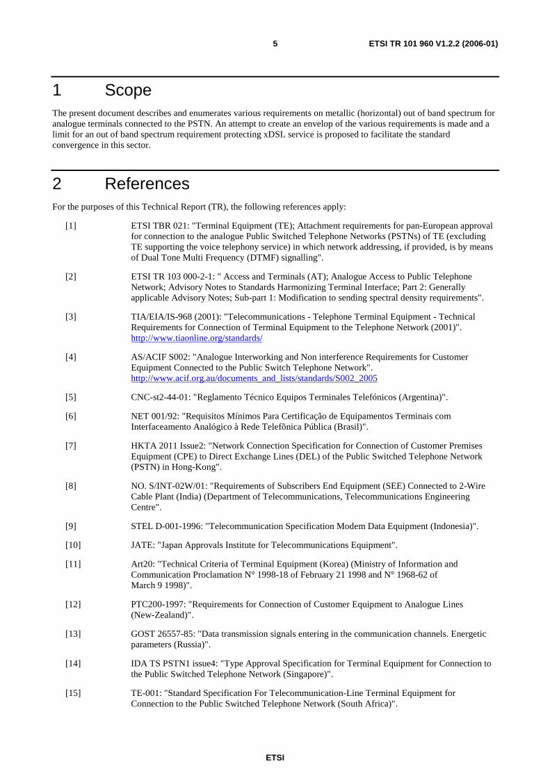
4.1 TBR 021 Requirement: As described in TBR 021 [1], clause 4.7.3.4 the total voltage level in a bandwidth, defined in table 4.1, wholly contained within the frequency range 4,3 kHz to 200 kHz, arising from normal operation of the TE when in an on-line, non-dialling state, and when terminated with ZR, shall not exceed the limits shown in table 4.1 and figure 4.1.
Table 4.1: Maximum sending level above 4,3 kHz
Points Frequency range (kHz)
Maximum sending level U in a specified
bandwidth (dBV)
Spectral Voltage U/√√√√B (dBV/√√√√Hz)
Measurement bandwidth (B)
Reference impedance
G to H 4,3 to 5,1 -40 decreasing to -44 -64,8 decreasing to -68,8 300 Hz ZR
H to I 5,1 to 8,9 -44 -68,8 300 Hz ZR
I to J 8,9 to 11 -44 decreasing to -58,5 -68,8 decreasing to -83,3 300 Hz ZR
J to K 11 to 200 -58,5 -88,5 1 kHz ZR
NOTE: Limits for intermediate frequencies can be found by drawing a straight line between the break points on a logarithmic (Hz) - linear (dB) scale.
-40
-44
-58,5
dBV
kHz4,3 5,1 8,9 200
G
H I
J K
300 Hz 1 kHz Measurementbandwidth
Maximum sending level (dBV)in measurement bandwidth
Not to scale
11
Figure 4.1: Maximum sending level above 4,3 kHz
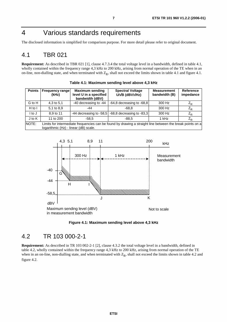
4.2 TR 103 000-2-1 Requirement: As described in TR 103 002-2-1 [2], clause 4.3.2 the total voltage level in a bandwidth, defined in table 4.2, wholly contained within the frequency range 4,3 kHz to 200 kHz, arising from normal operation of the TE when in an on-line, non-dialling state, and when terminated with ZR, shall not exceed the limits shown in table 4.2 and
figure 4.2.
ETSI
ETSI TR 101 960 V1.2.2 (2006-01) 8
Table 4.2: Maximum sending level above 4,3 kHz
Points Frequency range (kHz)
Maximum sending level U in a specified
bandwidth (dBV)
Spectral Voltage U/√√√√B (dBV/√√√√Hz)
Measurement bandwidth (B)
Reference impedance
G to H 4,3 to 6,0 -15 -39,8 300 Hz ZR
H to I 6,0 to 8,9 -15 decreasing to -44 -39,8 decreasing to -68,8
300 Hz ZR
I to J 8,9 to 12 -44 decreasing to -58,5
-68,8 decreasing to -83,3
300 Hz ZR
J to K 12 to 200 -58,5 -88,5 1 kHz ZR
NOTE: Limits for intermediate frequencies can be found by drawing a straight line between the break points on a logarithmic (Hz) - linear (dB) scale.
-15
-44
-58,5
dBV
kHz4,3 6,0 8,9 200
G H
I
J K
300 Hz 1 kHz
Measurementbandwidth
Maximum sending level (dBV)in measurement bandwidth
Not to scale
12
Figure 4.2: Maximum sending level above 4,3 kHz
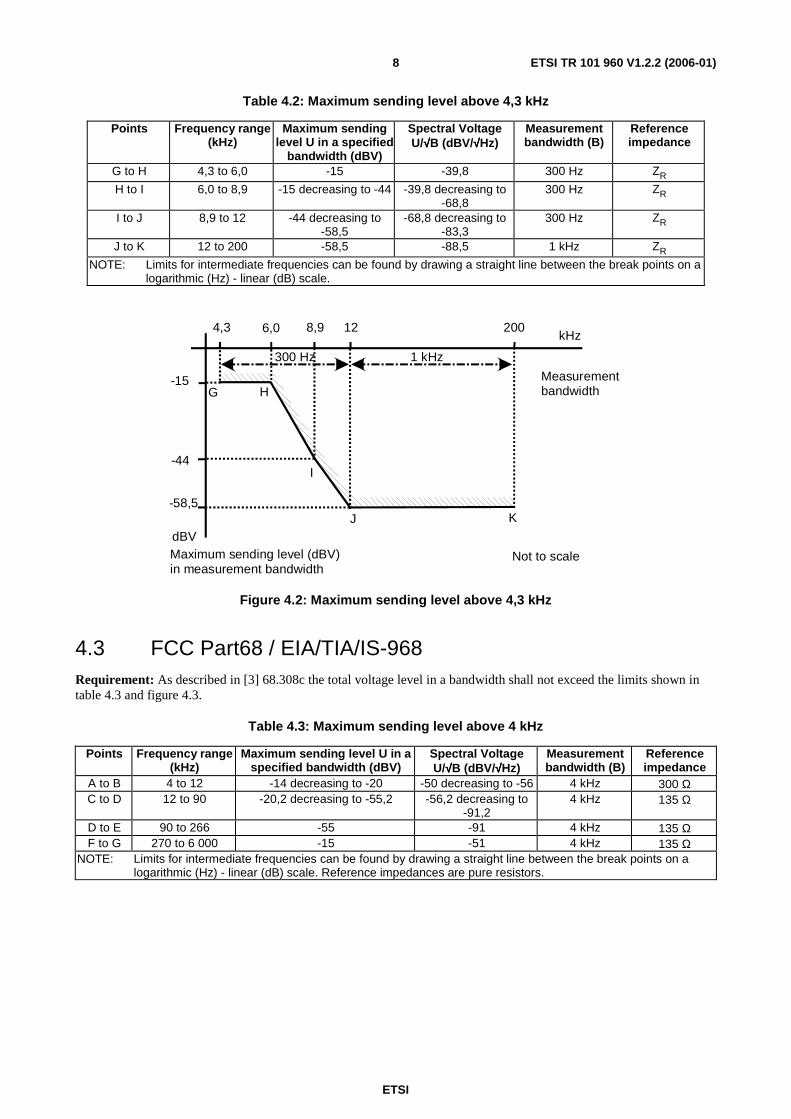
4.3 FCC Part68 / EIA/TIA/IS-968 Requirement: As described in [3] 68.308c the total voltage level in a bandwidth shall not exceed the limits shown in table 4.3 and figure 4.3.
Table 4.3: Maximum sending level above 4 kHz
Points Frequency range (kHz)
Maximum sending level U in a specified bandwidth (dBV)
Spectral Voltage U/√√√√B (dBV/√√√√Hz)
Measurement bandwidth (B)
Reference impedance
A to B 4 to 12 -14 decreasing to -20 -50 decreasing to -56 4 kHz 300 Ω C to D 12 to 90 -20,2 decreasing to -55,2 -56,2 decreasing to
-91,2 4 kHz 135 Ω
D to E 90 to 266 -55 -91 4 kHz 135 Ω F to G 270 to 6 000 -15 -51 4 kHz 135 Ω
NOTE: Limits for intermediate frequencies can be found by drawing a straight line between the break points on a logarithmic (Hz) - linear (dB) scale. Reference impedances are pure resistors.
ETSI
ETSI TR 101 960 V1.2.2 (2006-01) 9
E
B
A C
D
F G
-60
-50
-40
-30
-20
-10
0 1 10 100 1 000 10 000
kHz
dB
V
Figure 4.3: Maximum sending level above 4 kHz
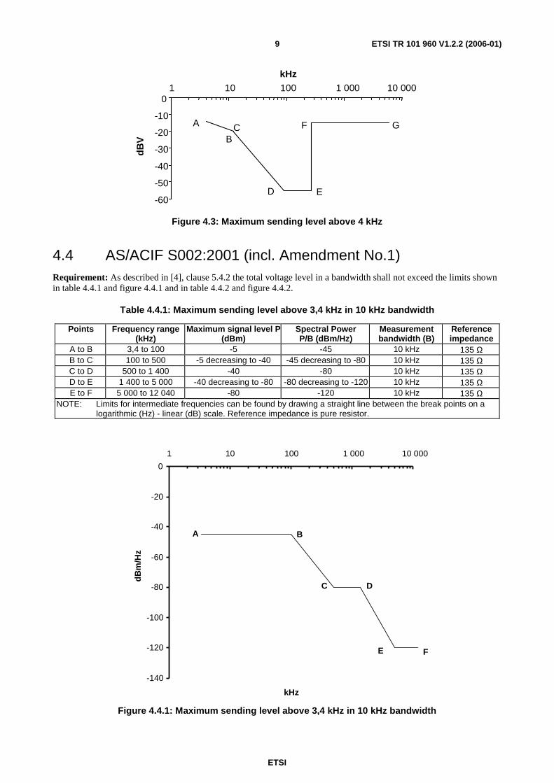
4.4 AS/ACIF S002:2001 (incl. Amendment No.1) Requirement: As described in [4], clause 5.4.2 the total voltage level in a bandwidth shall not exceed the limits shown in table 4.4.1 and figure 4.4.1 and in table 4.4.2 and figure 4.4.2.
Table 4.4.1: Maximum sending level above 3,4 kHz in 10 kHz bandwidth
Points Frequency range (kHz)
Maximum signal level P(dBm)
Spectral Power P/B (dBm/Hz)
Measurement bandwidth (B)
Reference impedance
A to B 3,4 to 100 -5 -45 10 kHz 135 Ω B to C 100 to 500 -5 decreasing to -40 -45 decreasing to -80 10 kHz 135 Ω C to D 500 to 1 400 -40 -80 10 kHz 135 Ω D to E 1 400 to 5 000 -40 decreasing to -80 -80 decreasing to -120 10 kHz 135 Ω E to F 5 000 to 12 040 -80 -120 10 kHz 135 Ω
NOTE: Limits for intermediate frequencies can be found by drawing a straight line between the break points on a logarithmic (Hz) - linear (dB) scale. Reference impedance is pure resistor.
F E
D C
B A
-140
-120
-100
-80
-60
-40
-20
0
1 10 100 1 000 10 000
kHz
dB
m/H
z
Figure 4.4.1: Maximum sending level above 3,4 kHz in 10 kHz bandwidth
ETSI
ETSI TR 101 960 V1.2.2 (2006-01) 10
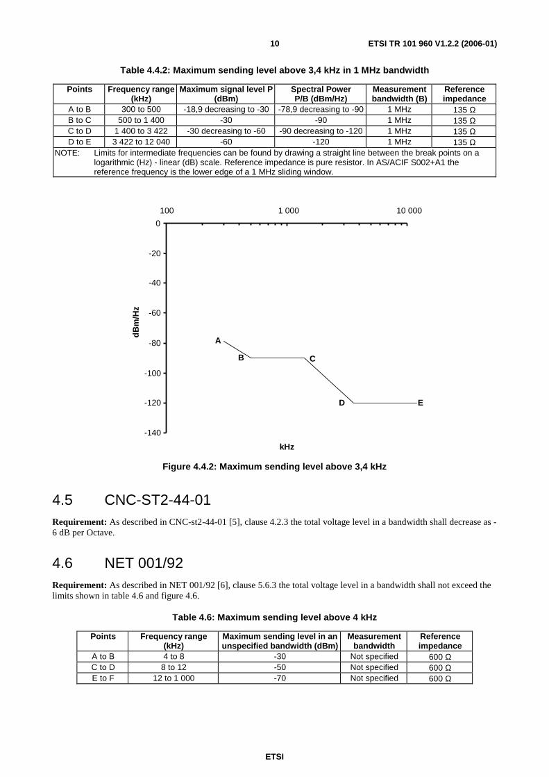
Table 4.4.2: Maximum sending level above 3,4 kHz in 1 MHz bandwidth
Points Frequency range (kHz)
Maximum signal level P (dBm)
Spectral Power P/B (dBm/Hz)
Measurement bandwidth (B)
Reference impedance
A to B 300 to 500 -18,9 decreasing to -30 -78,9 decreasing to -90 1 MHz 135 Ω B to C 500 to 1 400 -30 -90 1 MHz 135 Ω C to D 1 400 to 3 422 -30 decreasing to -60 -90 decreasing to -120 1 MHz 135 Ω D to E 3 422 to 12 040 -60 -120 1 MHz 135 Ω
NOTE: Limits for intermediate frequencies can be found by drawing a straight line between the break points on a logarithmic (Hz) - linear (dB) scale. Reference impedance is pure resistor. In AS/ACIF S002+A1 the reference frequency is the lower edge of a 1 MHz sliding window.
E D
C B
A
-140
-120
-100
-80
-60
-40
-20
0
100 1 000 10 000
kHz
dB
m/H
z
Figure 4.4.2: Maximum sending level above 3,4 kHz
4.5 CNC-ST2-44-01 Requirement: As described in CNC-st2-44-01 [5], clause 4.2.3 the total voltage level in a bandwidth shall decrease as -6 dB per Octave.
4.6 NET 001/92 Requirement: As described in NET 001/92 [6], clause 5.6.3 the total voltage level in a bandwidth shall not exceed the limits shown in table 4.6 and figure 4.6.
Table 4.6: Maximum sending level above 4 kHz
Points Frequency range (kHz)
Maximum sending level in an unspecified bandwidth (dBm)
Measurement bandwidth
Reference impedance
A to B 4 to 8 -30 Not specified 600 Ω C to D 8 to 12 -50 Not specified 600 Ω E to F 12 to 1 000 -70 Not specified 600 Ω

ETSI
ETSI TR 101 960 V1.2.2 (2006-01) 11
F
D
B
E
C
A
-80
-70
-60
-50
-40
-30
-20
-10
0 1 10 100 1 000
kHz
dB
m
Figure 4.6: Maximum sending level above 4 kHz
4.7 HKTA 2011 Issue2 Requirement: As described in [7], clause 3.4 the total voltage level in a bandwidth shall not exceed the limits shown in table 4.7 and figure 4.7.
Table 4.7: Maximum sending level above 4 kHz
Points Center frequency in (kHz)
Maximum sending level U in a specified bandwidth (dBV)
Spectral Voltage U/√√√√B (dBV/√√√√Hz)
Measurement bandwidth (B)
Reference impedance
A to B 8 to 12 -17,8 decreasing to -20 -56,8 decreasing to -59
8 kHz 300 Ω
B to C 12 to 90 -20 decreasing to -55,1 -59 decreasing to -94,1
8 kHz 135 Ω
D to E 90 to 266 -55 -94 8 kHz 135 Ω NOTE: Limits for intermediate frequencies can be found by drawing a straight line between the break points on a
logarithmic (Hz) - linear (dB) scale. Reference impedances are pure resistors.
E
A B
D C
-60
-50
-40
-30
-20
-10
0 1 10 100 1 000 kHz
dB
V
Figure 4.7: Maximum sending level above 4 kHz
ETSI
ETSI TR 101 960 V1.2.2 (2006-01) 12
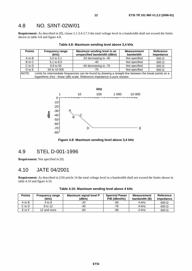
4.8 NO. S/INT-02W/01 Requirement: As described in [8], clause 2.1.3.4.3.7.3 the total voltage level in a bandwidth shall not exceed the limits shown in table 4.8 and figure 4.8.
Table 4.8: Maximum sending level above 3,4 kHz
Points Frequency range (kHz)
Maximum sending level in an unspecified bandwidth (dBm)
Measurement bandwidth
Reference Impedance
A to B 3,4 to 5,1 -33 decreasing to -40 Not specified 600 Ω B to C 5,1 to 8,9 -40 Not specified 600 Ω C to D 8,9 to 50 -40 decreasing to -70 Not specified 600 Ω D to E 50 to 10 000 -70 Not specified 600 Ω
NOTE: Limits for intermediate frequencies can be found by drawing a straight line between the break points on a logarithmic (Hz) - linear (dB) scale. Reference impedance is pure resistor.
E
C B
A
D -80 -70 -60 -50 -40 -30 -20 -10
0 1 10 100 1 000 10 000
kHz
dB
m
Figure 4.8: Maximum sending level above 3,4 kHz
4.9 STEL D-001-1996 Requirement: Not specified in [9].
4.10 JATE 04/2001 Requirement: As described in [10] article 14 the total voltage level in a bandwidth shall not exceed the limits shown in table 4.10 and figure 4.10.
Table 4.10: Maximum sending level above 4 kHz
Points Frequency range (kHz)
Maximum signal level P (dBm)
Spectral Power P/B (dBm/Hz)
Measurement bandwidth (B)
Reference impedance
A to B 4 to 8 -20 -56 4 kHz 600 Ω C to D 8 to 12 -40 -76 4 kHz 600 Ω E to F 12 and more -60 -96 4 kHz 600 Ω
ETSI
ETSI TR 101 960 V1.2.2 (2006-01) 13
F
D
B A
C
E
-70
-60
-50
-40
-30
-20
-10
0 1 10 100 1 000
kHz
dB
m
Figure 4.10: Maximum sending level above 4 kHz
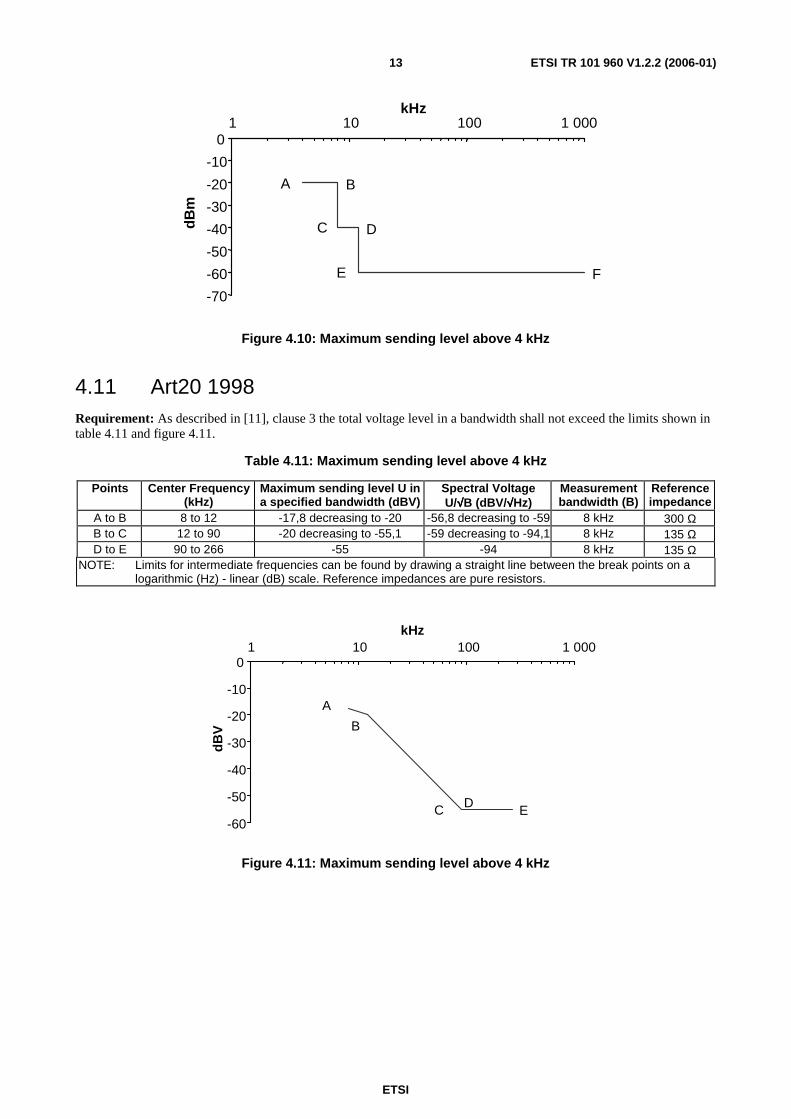
4.11 Art20 1998 Requirement: As described in [11], clause 3 the total voltage level in a bandwidth shall not exceed the limits shown in table 4.11 and figure 4.11.
Table 4.11: Maximum sending level above 4 kHz
Points Center Frequency (kHz)
Maximum sending level U in a specified bandwidth (dBV)
Spectral Voltage U/√√√√B (dBV/√√√√Hz)
Measurement bandwidth (B)
Reference impedance
A to B 8 to 12 -17,8 decreasing to -20 -56,8 decreasing to -59 8 kHz 300 Ω B to C 12 to 90 -20 decreasing to -55,1 -59 decreasing to -94,1 8 kHz 135 Ω D to E 90 to 266 -55 -94 8 kHz 135 Ω
NOTE: Limits for intermediate frequencies can be found by drawing a straight line between the break points on a logarithmic (Hz) - linear (dB) scale. Reference impedances are pure resistors.
E
A
B
D C -60
-50
-40
-30
-20
-10
0 1 10 100 1 000
kHz
dB
V
Figure 4.11: Maximum sending level above 4 kHz
ETSI
ETSI TR 101 960 V1.2.2 (2006-01) 14
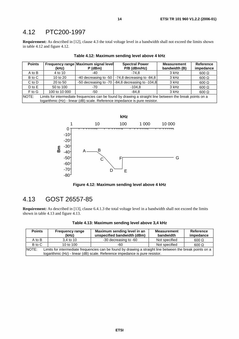
4.12 PTC200-1997 Requirement: As described in [12], clause 4.3 the total voltage level in a bandwidth shall not exceed the limits shown in table 4.12 and figure 4.12.
Table 4.12: Maximum sending level above 4 kHz
Points Frequency range (kHz)
Maximum signal level P (dBm)
Spectral Power P/B (dBm/Hz)
Measurement bandwidth (B)
Reference impedance
A to B 4 to 10 -40 -74,8 3 kHz 600 Ω B to C 10 to 20 -40 decreasing to -50 -74,8 decreasing to -84,8 3 kHz 600 Ω C to D 20 to 50 -50 decreasing to -70 -84,8 decreasing to -104,8 3 kHz 600 Ω D to E 50 to 100 -70 -104,8 3 kHz 600 Ω F to G 100 to 10 000 -50 -84,8 3 kHz 600 Ω
NOTE: Limits for intermediate frequencies can be found by drawing a straight line between the break points on a logarithmic (Hz) - linear (dB) scale. Reference impedance is pure resistor.
G
E
B A
C F
D -80 -70 -60 -50 -40 -30 -20 -10
0 1 10 100 1 000 10 000
kHz
Bm
Figure 4.12: Maximum sending level above 4 kHz
4.13 GOST 26557-85 Requirement: As described in [13], clause 6.4.1.3 the total voltage level in a bandwidth shall not exceed the limits shown in table 4.13 and figure 4.13.
Table 4.13: Maximum sending level above 3,4 kHz
Points Frequency range (kHz)
Maximum sending level in an unspecified bandwidth (dBm)
Measurement bandwidth
Reference impedance
A to B 3,4 to 10 -30 decreasing to -60 Not specified 600 Ω B to C 10 to 100 -60 Not specified 600 Ω
NOTE: Limits for intermediate frequencies can be found by drawing a straight line between the break points on a logarithmic (Hz) - linear (dB) scale. Reference impedance is pure resistor.

ETSI
ETSI TR 101 960 V1.2.2 (2006-01) 15
A
B C
-70
-60
-50
-40
-30
-20
-10
0
1 10 100
kHz
dB
m
Figure 4.13: Maximum sending level above 3,4 kHz
4.14 IDA TS PSTN1 issue4 2000 Requirement: As described in [14], clause 6.4.1.3 the total voltage level in a bandwidth shall not exceed the limits shown in table 4.14 and figure 4.14.
Table 4.14: Maximum sending level above 3,4 kHz
Points Frequency range (kHz)
Maximum sending level in an unspecified bandwidth (dBm)
Measurement bandwidth
Reference Impedance
A to B 3,4 to 50 -33 Not specified 600 Ω C to D 50 to 200 -70 Not specified 600 Ω
NOTE: Reference impedance is pure resistor.
kHz
D C
B A
- 80
- 70
- 60
- 50
- 40
- 30
- 20
- 10
0 1 10 100 1 000
Bm
Figure 4.14: Maximum sending level above 3,4 kHz
ETSI
ETSI TR 101 960 V1.2.2 (2006-01) 16
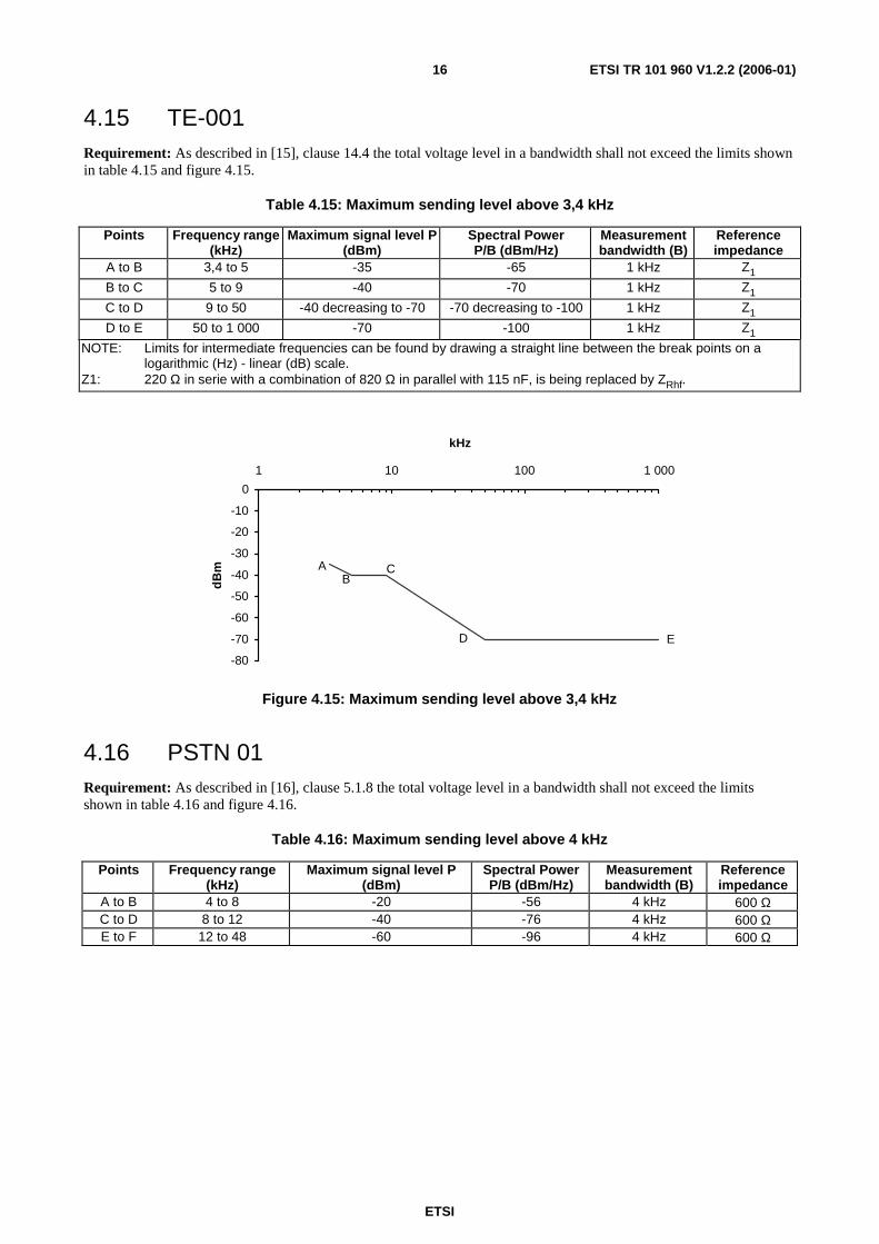
4.15 TE-001 Requirement: As described in [15], clause 14.4 the total voltage level in a bandwidth shall not exceed the limits shown in table 4.15 and figure 4.15.
Table 4.15: Maximum sending level above 3,4 kHz
Points Frequency range (kHz)
Maximum signal level P (dBm)
Spectral Power P/B (dBm/Hz)
Measurement bandwidth (B)
Reference impedance
A to B 3,4 to 5 -35 -65 1 kHz Z1
B to C 5 to 9 -40 -70 1 kHz Z1
C to D 9 to 50 -40 decreasing to -70 -70 decreasing to -100 1 kHz Z1
D to E 50 to 1 000 -70 -100 1 kHz Z1
NOTE: Limits for intermediate frequencies can be found by drawing a straight line between the break points on a logarithmic (Hz) - linear (dB) scale.
Z1: 220 Ω in serie with a combination of 820 Ω in parallel with 115 nF, is being replaced by ZRhf.
E
C B
A
D -80 -70 -60 -50 -40 -30 -20 -10
0 1 10 100 1 000
kHz
dB
m
Figure 4.15: Maximum sending level above 3,4 kHz
4.16 PSTN 01 Requirement: As described in [16], clause 5.1.8 the total voltage level in a bandwidth shall not exceed the limits shown in table 4.16 and figure 4.16.
Table 4.16: Maximum sending level above 4 kHz
Points Frequency range (kHz)
Maximum signal level P (dBm)
Spectral Power P/B (dBm/Hz)
Measurement bandwidth (B)
Reference impedance
A to B 4 to 8 -20 -56 4 kHz 600 Ω C to D 8 to 12 -40 -76 4 kHz 600 Ω E to F 12 to 48 -60 -96 4 kHz 600 Ω

ETSI
ETSI TR 101 960 V1.2.2 (2006-01) 17
F
D
B A
C
E
-70
-60
-50
-40
-30
-20
-10
0 1 10 100
kHz
dB
m
Figure 4.16: Maximum sending level above 4 kHz
4.17 Estimated POTS model from TR 101 830-1 Description: As described in [17], clause 8.1.3 the total voltage level in a bandwidth is estimated not to exceed the limits shown in table 4.17 and figure 4.17.
Table 4.17: Break points of the narrow-band voltage limits
Frequency (F)
Impedance (Z)
Signal Level (U)
Power Bandwidth (B)
Spectral Voltage (U/√√√√B)
30 Hz ZR -33,7 dBV 10 Hz -43,7 dBV/√Hz 100 Hz ZR -10,7 dBV 10 Hz -20,7 dBV/√Hz 200 Hz ZR -6,7 dBV 10 Hz -16,7 dBV/√Hz 3,8 kHz ZR -6,7 dBV 10 Hz -16,7 dBV/√Hz 3,9 kHz ZR -10,7 dBV 10 Hz -20,7 dBV/√Hz 4,0 kHz ZR -16,7 dBV 10 Hz -26,7 dBV/√Hz 4,3 kHz ZR -44,7 dBV 10 Hz -54,7 dBV/√Hz 4,3 kHz ZR -40 dBV 300 Hz -65 dBV/√Hz 5,1 kHz ZR -44 dBV 300 Hz -69 dBV/√Hz 8,9 kHz ZR -44 dBV 300 Hz -69 dBV/√Hz
11,0 kHz ZR -58,5 dBV 300 Hz -83,5 dBV/√Hz 11,0 kHz ZR -58,5 dBV 1 kHz -88,5 dBV/√Hz 200 kHz ZR -58,5 dBV 1 kHz -88,5 dBV/√Hz
200 kHz 135 Ω -60 dBV 1 kHz -90 dBV/√Hz 500 kHz 135 Ω -90 dBV 1 kHz -120 dBV/√Hz 500 kHz 135 Ω -60 dBV 1 MHz -120 dBV/√Hz 30 MHz 135 Ω -60 dBV 1 MHz -120 dBV/√Hz
NOTE: A voltage of 1 V, equals 0 dBV, and causes a power of +2,2 dBm in 600 Ω and +8,7 dBm in 135 Ω.

ETSI
ETSI TR 101 960 V1.2.2 (2006-01) 18
Spectral Voltage of POTS signals
-140
-120
-100
-80
-60
-40
-20
0
0,1 1 10 100 1000 10000frequency [kHz]
[dB
V /
sqrt
(Hz)
]
Figure 4.17: Spectral Voltage for POTS signal
5 Comparison attempt between 10 kHz and 10 MHz Hypothesis:
• All limits are translated into a dBm/Hz scale.
• Whenever Rbw is not defined in the specification, it is supposed to be 1 kHz.
NOTE: Those values are derived from formal documents but might not correspond exactly to the national applicable requirement because in some case assumption were made to overcome insufficient information (e.g. rbw definition).
It is not possible to directly compare various out of band spectrum requirements using different reference impedances and various resolution bandwidth. Three big categories are present:
• 135 Ω reference and narrow resolution bandwidth (less than 10 kHz).
• 135 Ω reference impedance and large resolution bandwidth (1 MHz).
• 600 Ω reference impedance and narrow resolution bandwidth (less than 10 kHz).

ETSI
ETSI TR 101 960 V1.2.2 (2006-01) 19
Above 10 kHz complexe impedance like Zr are considered as being reduced to their real part. For Zr it is 270 Ω.
Outband Spectrum Comparison 135 ΩΩΩΩ / small rbw
ACIF S002
TS 103 021 TBR21
US EIA/TIA
ADSL / 100 Ω
ETSI Proposal clause 6
-140
-120
-100
-80
-60
-40
-20
0 10 100 1 000 10 000 100 000
kHz
dB
m/H
z
Figure 5a
ETSI
ETSI TR 101 960 V1.2.2 (2006-01) 20
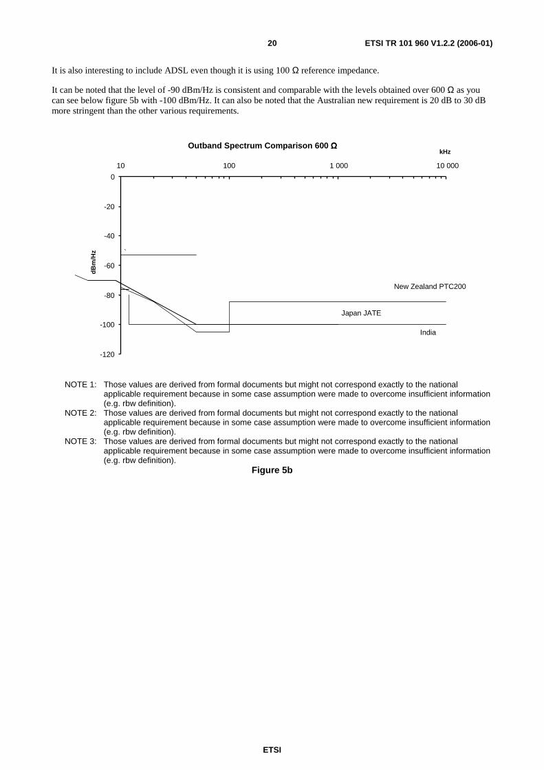
It is also interesting to include ADSL even though it is using 100 Ω reference impedance.
It can be noted that the level of -90 dBm/Hz is consistent and comparable with the levels obtained over 600 Ω as you can see below figure 5b with -100 dBm/Hz. It can also be noted that the Australian new requirement is 20 dB to 30 dB more stringent than the other various requirements.
Outband Spectrum Comparison 600 ΩΩΩΩ
India
Japan JATE
New Zealand PTC200
-120
-100
-80
-60
-40
-20
0 10 100 1 000 10 000
kHz
dB
m/H
z
NOTE 1: Those values are derived from formal documents but might not correspond exactly to the national applicable requirement because in some case assumption were made to overcome insufficient information (e.g. rbw definition).
NOTE 2: Those values are derived from formal documents but might not correspond exactly to the national applicable requirement because in some case assumption were made to overcome insufficient information (e.g. rbw definition).
NOTE 3: Those values are derived from formal documents but might not correspond exactly to the national applicable requirement because in some case assumption were made to overcome insufficient information (e.g. rbw definition).
Figure 5b
ETSI
ETSI TR 101 960 V1.2.2 (2006-01) 21
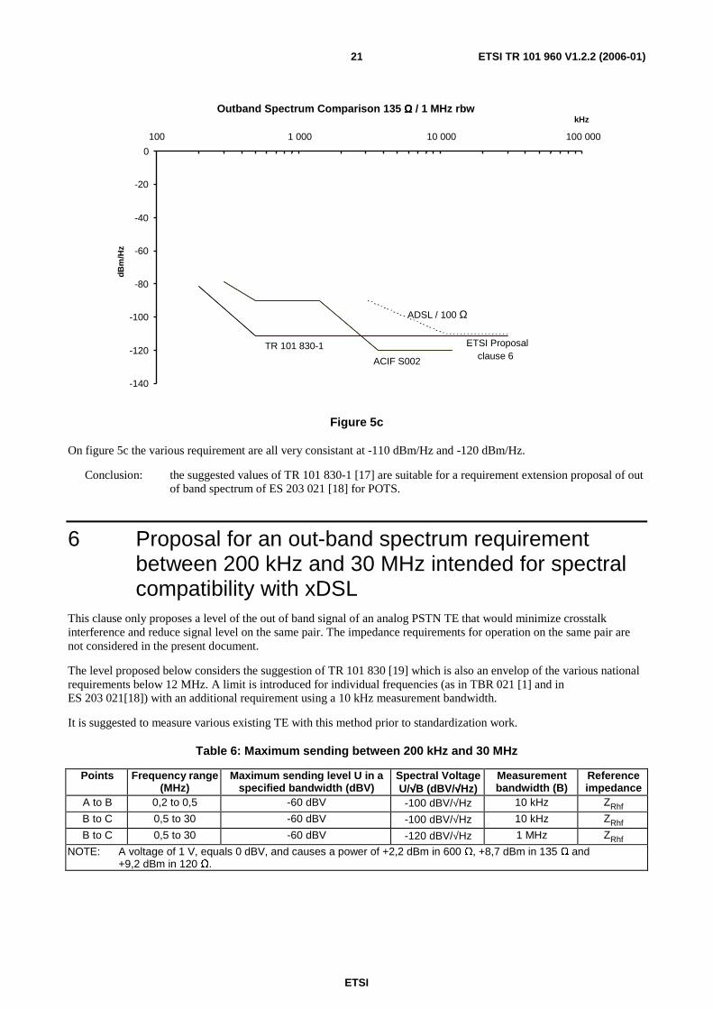
Outband Spectrum Comparison 135 ΩΩΩΩ / 1 MHz rbw
ACIF S002 ETSI Proposal
clause 6
ADSL / 100 Ω
TR 101 830-1
-140
-120
-100
-80
-60
-40
-20
0 100 1 000 10 000 100 000
kHz d
Bm
/Hz
Figure 5c
On figure 5c the various requirement are all very consistant at -110 dBm/Hz and -120 dBm/Hz.
Conclusion: the suggested values of TR 101 830-1 [17] are suitable for a requirement extension proposal of out of band spectrum of ES 203 021 [18] for POTS.
6 Proposal for an out-band spectrum requirement between 200 kHz and 30 MHz intended for spectral compatibility with xDSL
This clause only proposes a level of the out of band signal of an analog PSTN TE that would minimize crosstalk interference and reduce signal level on the same pair. The impedance requirements for operation on the same pair are not considered in the present document.
The level proposed below considers the suggestion of TR 101 830 [19] which is also an envelop of the various national requirements below 12 MHz. A limit is introduced for individual frequencies (as in TBR 021 [1] and in ES 203 021[18]) with an additional requirement using a 10 kHz measurement bandwidth.
It is suggested to measure various existing TE with this method prior to standardization work.
Table 6: Maximum sending between 200 kHz and 30 MHz
Points Frequency range (MHz)
Maximum sending level U in a specified bandwidth (dBV)
Spectral Voltage U/√√√√B (dBV/√√√√Hz)
Measurement bandwidth (B)
Reference impedance
A to B 0,2 to 0,5 -60 dBV -100 dBV/√Hz 10 kHz ZRhf
B to C 0,5 to 30 -60 dBV -100 dBV/√Hz 10 kHz ZRhf
B to C 0,5 to 30 -60 dBV -120 dBV/√Hz 1 MHz ZRhf
NOTE: A voltage of 1 V, equals 0 dBV, and causes a power of +2,2 dBm in 600 Ω, +8,7 dBm in 135 Ω and +9,2 dBm in 120 Ω.

ETSI
ETSI TR 101 960 V1.2.2 (2006-01) 22
7 Conclusion The possibility of a common measurement method and a limit value for the frequency domain of the requirements is discussed and suggestions for future global standardization work specified.
The information in the present document should be of assistance for spectrum management studies, PSTN and xDSL devices (terminals and conventional line access equipment).
Due to the fact that many parameters e.g. test impedance, resolution bandwidth the proposal for harmonization should not be definitely taken. Before standardization work establishes harmonized values it is extremely important to confirm (e.g. by field tests) that the suggested values are appropriate.

ETSI
ETSI TR 101 960 V1.2.2 (2006-01) 23
Annex A: Reference Impedances
A.1 Reference Impedance ZR
270 Ω
750 Ω
150 nF
Figure A.1: Reference impedance ZR
A.2 Reference Impedance ZRhf
120 ΩΩΩΩ 150 ΩΩΩΩ 750 ΩΩΩΩ
Figure A.2

ETSI
ETSI TR 101 960 V1.2.2 (2006-01) 24
History
Document history
V1.1.1 May 2002 Publication
V1.2.1 January 2004 Publication
V1.2.2 January 2006 Publication