Embed Size (px)
Citation preview
3PEAK
1
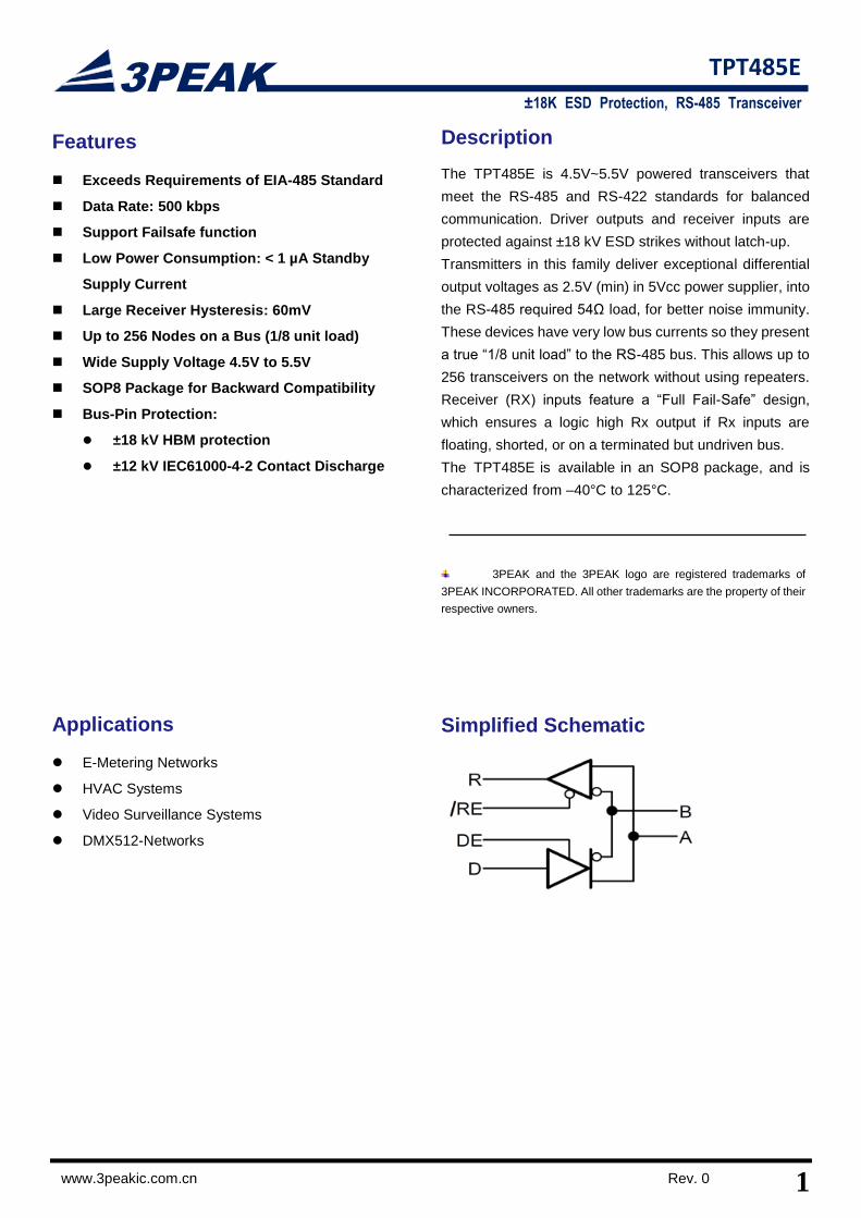
TPT485E
± 18K ESD Protection, RS-485 Transceiver
www.3peakic.com.cn Rev. 0
Features
Exceeds Requirements of EIA-485 Standard
Data Rate: 500 kbps
Support Failsafe function
Low Power Consumption: < 1 µA Standby
Supply Current
Large Receiver Hysteresis: 60mV
Up to 256 Nodes on a Bus (1/8 unit load)
Wide Supply Voltage 4.5V to 5.5V
SOP8 Package for Backward Compatibility
Bus-Pin Protection:
±18 kV HBM protection
±12 kV IEC61000-4-2 Contact Discharge
Applications
E-Metering Networks
HVAC Systems
Video Surveillance Systems
DMX512-Networks
Description
The TPT485E is 4.5V~5.5V powered transceivers that
meet the RS-485 and RS-422 standards for balanced
communication. Driver outputs and receiver inputs are
protected against ±18 kV ESD strikes without latch-up.
Transmitters in this family deliver exceptional differential
output voltages as 2.5V (min) in 5Vcc power supplier, into
the RS-485 required 54Ω load, for better noise immunity.
These devices have very low bus currents so they present
a true “1/8 unit load” to the RS-485 bus. This allows up to
256 transceivers on the network without using repeaters.
Receiver (RX) inputs feature a “Full Fail-Safe” design,
which ensures a logic high Rx output if Rx inputs are
floating, shorted, or on a terminated but undriven bus.
The TPT485E is available in an SOP8 package, and is
characterized from –40°C to 125°C.
3PEAK and the 3PEAK logo are registered trademarks of
3PEAK INCORPORATED. All other trademarks are the property of their
respective owners.
Simplified Schematic
2 Rev. 0 www.3peakic.com.cn
TPT485E
± 18K ESD Protection, RS-485 Transceiver
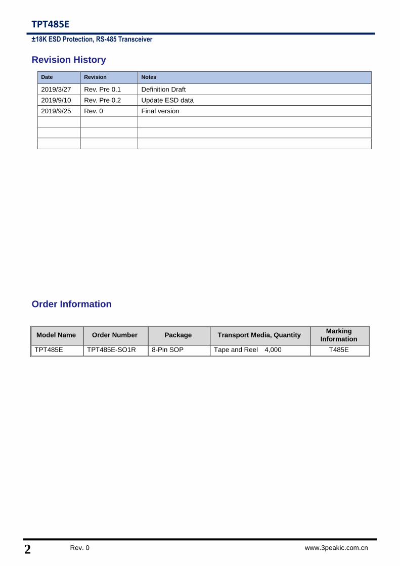
Revision History
Date Revision Notes
2019/3/27 Rev. Pre 0.1 Definition Draft
2019/9/10 Rev. Pre 0.2 Update ESD data
2019/9/25 Rev. 0 Final version
Order Information
Model Name Order Number Package Transport Media, Quantity Marking
Information
TPT485E TPT485E-SO1R 8-Pin SOP Tape and Reel 4,000 T485E
3
TPT485E
± 18K ESD Protection, RS-485 Transceiver
www.3peakic.com.cn Rev. 0
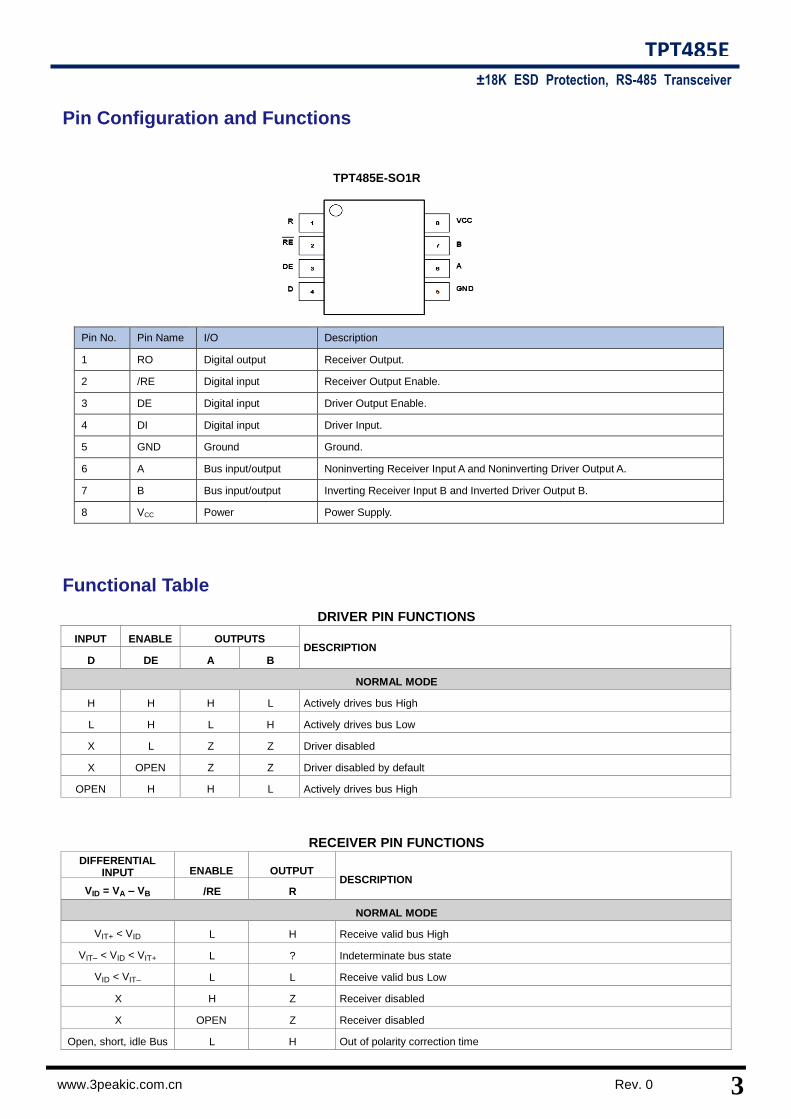
Pin Configuration and Functions
Pin No. Pin Name I/O Description
1 RO Digital output Receiver Output.
2 /RE Digital input Receiver Output Enable.
3 DE Digital input Driver Output Enable.
4 DI Digital input Driver Input.
5 GND Ground Ground.
6 A Bus input/output Noninverting Receiver Input A and Noninverting Driver Output A.
7 B Bus input/output Inverting Receiver Input B and Inverted Driver Output B.
8 VCC Power Power Supply.
Functional Table
DRIVER PIN FUNCTIONS
INPUT ENABLE OUTPUTS
DESCRIPTION
D DE A B
NORMAL MODE
H H H L Actively drives bus High
L H L H Actively drives bus Low
X L Z Z Driver disabled
X OPEN Z Z Driver disabled by default
OPEN H H L Actively drives bus High
RECEIVER PIN FUNCTIONS
DIFFERENTIAL INPUT
ENABLE
OUTPUT DESCRIPTION
VID = VA – VB /RE R
NORMAL MODE
VIT+ < VID L H Receive valid bus High
VIT– < VID < VIT+ L ? Indeterminate bus state
VID < VIT– L L Receive valid bus Low
X H Z Receiver disabled
X OPEN Z Receiver disabled
Open, short, idle Bus L H Out of polarity correction time
TPT485E-SO1R
4 Rev. 0 www.3peakic.com.cn
TPT485E
± 18K ESD Protection, RS-485 Transceiver
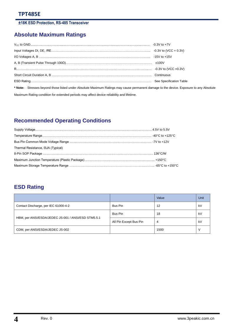
Absolute Maximum Ratings
VCC to GND......................................................................................................................................... -0.3V to +7V
Input Voltages DI, DE, /RE……………………………………………………….………………………..... -0.3V to (VCC + 0.3V)
I/O Voltages A, B ….......................…………………………………………………………………….…... -15V to +15V
A, B (Transient Pulse Through 100Ω)………………………………………………………….……….…… ±100V
R………………………………………………………………………………………………………….…..…. -0.3V to (VCC +0.3V)
Short Circuit Duration A, B …………………………………………………………………………….…….. Continuous
ESD Rating…………………………………………………………………………………………………..… See Specification Table
* Note: Stresses beyond those listed under Absolute Maximum Ratings may cause permanent damage to the device. Exposure to any Absolute
Maximum Rating condition for extended periods may affect device reliability and lifetime.
Recommended Operating Conditions
Supply Voltage………………………………………………………………………………….………..……. 4.5V to 5.5V
Temperature Range……………………………………………………………………………………...…… -40°C to +125°C
Bus Pin Common Mode Voltage Range ……………………………………………………………..…….. -7V to +12V
Thermal Resistance, ΘJA (Typical)
8-Pin SOP Package ………………………………………………………………….…………………...…… 136°C/W
Maximum Junction Temperature (Plastic Package) ……………………………………………...…………. +150°C
Maximum Storage Temperature Range …………………………………………………………..………….. -65°C to +150°C
ESD Rating
Value Unit
Contact Discharge, per IEC 61000-4-2 Bus Pin 12 kV
HBM, per ANSI/ESDA/JEDEC JS-001 / ANSI/ESD STM5.5.1
Bus Pin 18 kV
All Pin Except Bus Pin 4 kV
CDM, per ANSI/ESDA/JEDEC JS-002 1500 V
5
TPT485E
± 18K ESD Protection, RS-485 Transceiver
www.3peakic.com.cn Rev. 0
Electrical Characteristics
Test Conditions: VCC = 5V, Over operating free-air temperature range (unless otherwise noted)
Parameter Conditions Min Typ Max Units
Driver
|VOD| Driver differential-output voltage
magnitude
RL = 60 Ω,
-7V≤V test ≤12V See Figure 1B 2.0 3.5
V RL = 54 Ω (RS-485) See Figure 1A 2.0 3.4
RL = 100 Ω (RS-485) 2.7 3.7
⊿|VOD| Change in magnitude of driver
differential-output voltage RL = 54 Ω, CL=50pF See Figure 1A -50 50 mV
VOC(SS) Steady-stage common-mode
output voltage
Center of two 27-Ω
load resistors See Figure 1A
1 VCC/2 3 V
⊿VOC Change in differential driver
common-mode output voltage -65 65
mV
VOC(PP) Peak-to-peak driver common-
mode output voltage 600
|IOS| Driver short-circuit output current │IOS│ with A shorted to B 90 110 mA
Receiver
VIT+ Positive-going receiver differential-
input voltage threshold -100 -15 mV
VIT- Negative-going receiver
differential-input voltage threshold -240 -150 mV
VHYS(1)
Receiver differential-input voltage
threshold hysteresis (VIT+ – VIT– ) 60 mV
VIH Logic Input High Voltage DI, DE, RE 2 V
VIL Logic Input Low Voltage DI, DE, RE 0.8 V
VOH Receiver high-level output voltage IOH= -8 mA 4.0 VCC-0.3 V
VOL Receiver low-level output voltage IOL= 8 mA 0.2 0.4 V
Ii DE=0, VCC=0 or VCC=5.5V VI=12V 30 120 μA
VI=-7V -100 -50 μA
RA,RB Bus input impedance VA=-7V, VB=12V or VA=12V, VB=-7V 96 kΩ
IOZ Receiver high-impedance output
current VO = 0 V or VCC, /RE at VCC -1 1 μA
IOSR Receiver output short to ground
current REN=0, DE=VCC 80 95 mA
Logic
Iin Input current (RE, DE, D) 4.5V<VCC<5.5V -5 5 uA
Supply
ICC Supply current(quiescent)
Driver and receiver
enabled
DE = VCC, /RE =
GND, No LOAD 650 800
μA
Driver enabled,
receiver disabled
DE = /RE = VCC,
No LOAD 450 600
Driver disabled,
receiver enabled
DE = /RE = GND,
No LOAD 450 600
Driver and receiver
disabled
DE = GND, /RE =
D= VCC, No LOAD 0.5 2
6 Rev. 0 www.3peakic.com.cn
TPT485E
± 18K ESD Protection, RS-485 Transceiver
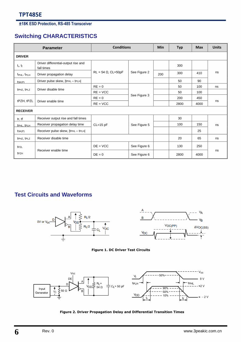
Switching CHARACTERISTICS
Test Circuits and Waveforms
Figure 1. DC Driver Test Circuits
Figure 2. Driver Propagation Delay and Differential Transition Times
Parameter Conditions Min Typ Max Units
DRIVER
tr, tf Driver differential-output rise and
fall times
RL = 54 Ω, CL=50pF See Figure 2
300
ns tPHL, tPLH
Driver propagation delay 200 300 410
tSK(P) Driver pulse skew, |tPHL – tPLH| 50 90
tPHZ, tPLZ Driver disable time RE = 0
See Figure 3
50 100 ns
RE = VCC 50 100
tPZH, tPZL Driver enable time RE = 0 200 450
ns RE = VCC 2800 4000
RECEIVER
tr, tf Receiver output rise and fall times
CL=15 pF See Figure 5
30
ns tPHL, tPLH Receiver propagation delay time 100 150
tSK(P) Receiver pulse skew, |tPHL – tPLH| 25
tPHZ, tPLZ Receiver disable time 20 65 ns
tPZL
tPZH Receiver enable time
DE = VCC See Figure 6 130 250
ns
DE = 0 See Figure 6 2800 4000
7
TPT485E
± 18K ESD Protection, RS-485 Transceiver
www.3peakic.com.cn Rev. 0
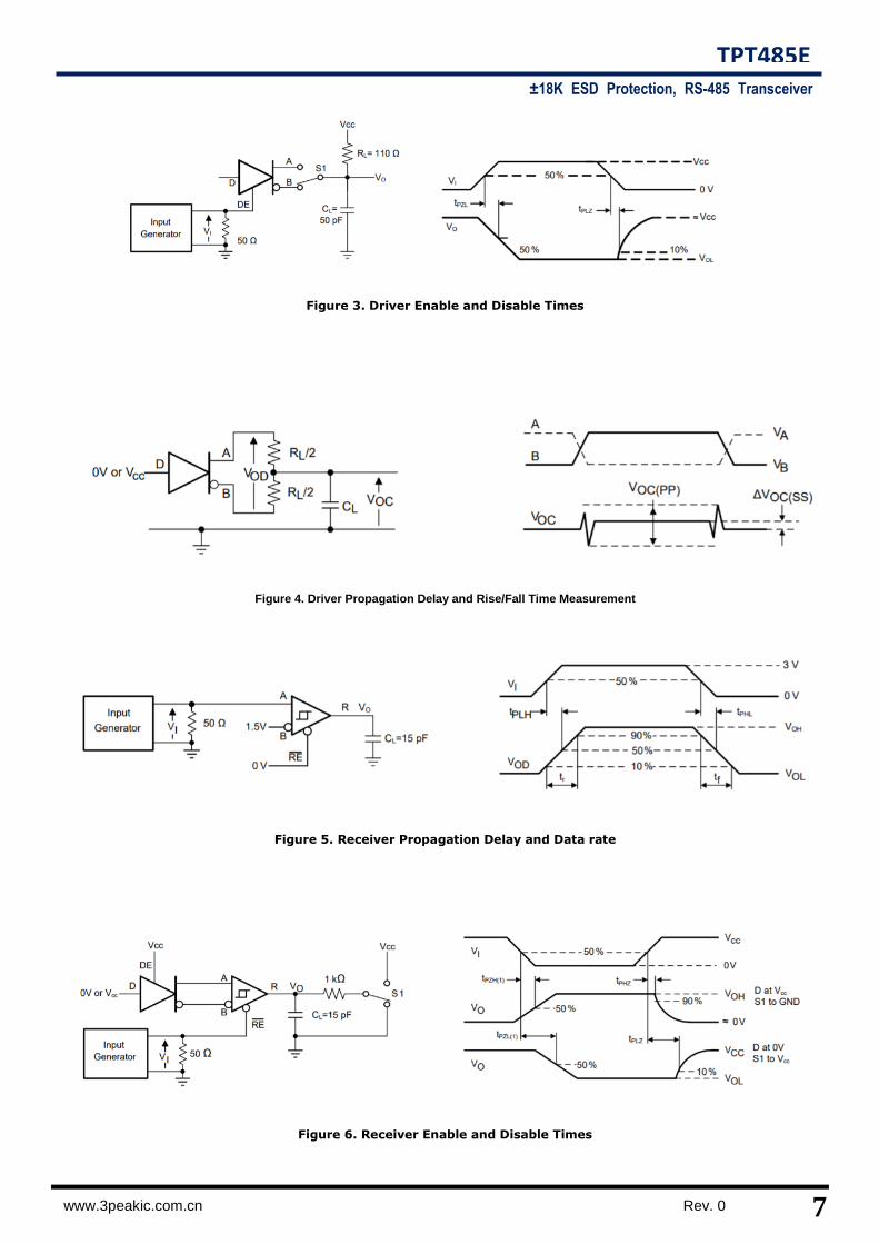
Figure 3. Driver Enable and Disable Times
Figure 4. Driver Propagation Delay and Rise/Fall Time Measurement
Figure 5. Receiver Propagation Delay and Data rate
Figure 6. Receiver Enable and Disable Times
8 Rev. 0 www.3peakic.com.cn
TPT485E
± 18K ESD Protection, RS-485 Transceiver
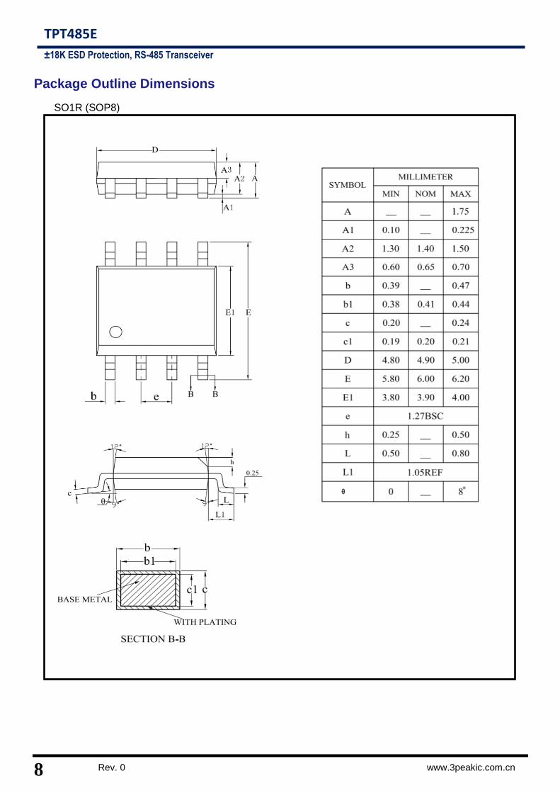
Package Outline Dimensions
SO1R (SOP8)