Embed Size (px)
Citation preview
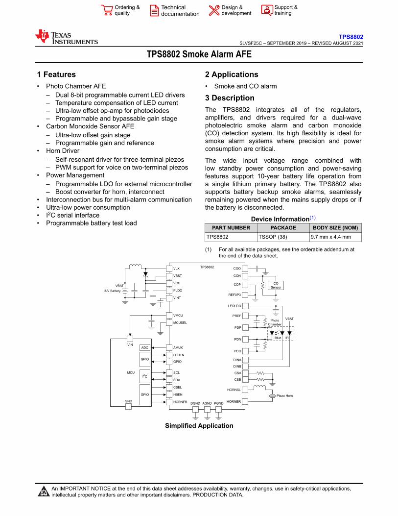
TPS8802 Smoke Alarm AFE
1 Features• Photo Chamber AFE
– Dual 8-bit programmable current LED drivers– Temperature compensation of LED current– Ultra-low offset op-amp for photodiodes– Programmable and bypassable gain stage
• Carbon Monoxide Sensor AFE– Ultra-low offset gain stage– Programmable gain and reference
• Horn Driver– Self-resonant driver for three-terminal piezos– PWM support for voice on two-terminal piezos
• Power Management– Programmable LDO for external microcontroller– Boost converter for horn, interconnect
• Interconnection bus for multi-alarm communication• Ultra-low power consumption• I2C serial interface• Programmable battery test load
2 Applications• Smoke and CO alarm
3 DescriptionThe TPS8802 integrates all of the regulators, amplifiers, and drivers required for a dual-wave photoelectric smoke alarm and carbon monoxide (CO) detection system. Its high flexibility is ideal for smoke alarm systems where precision and power consumption are critical.
The wide input voltage range combined with low standby power consumption and power-saving features support 10-year battery life operation from a single lithium primary battery. The TPS8802 also supports battery backup smoke alarms, seamlessly remaining powered when the mains supply drops or if the battery is disconnected.
Device Information(1)
PART NUMBER PACKAGE BODY SIZE (NOM)TPS8802 TSSOP (38) 9.7 mm x 4.4 mm
(1) For all available packages, see the orderable addendum at the end of the data sheet.
VBST
TPS8802
PLDO
AMUX
DGNDHORNBR
VCC
VINT
VMCU
MCUSEL
MCU
ADC
GPIO
I2C
GPIO
LEDEN
GPIO
SCL
SDA
CSEL
HBEN
HORNFB
VIN
AGND PGND
HORNSL
REF0P3
COP
CON
COO
CO
Sensor
VLX
3-V Battery
Piezo Horn
GND
VBAT
CSA
DINA
PDO
PDN
PDP
PREF
Photo
Chamber
LEDLDO
DINB
CSB
Blue IR
VBAT
Simplified Application
TPS8802SLVSF25C – SEPTEMBER 2019 – REVISED AUGUST 2021
An IMPORTANT NOTICE at the end of this data sheet addresses availability, warranty, changes, use in safety-critical applications, intellectual property matters and other important disclaimers. PRODUCTION DATA.
Table of Contents1 Features............................................................................12 Applications..................................................................... 13 Description.......................................................................14 Revision History.............................................................. 25 Pin Configuration and Functions...................................3
Pin Functions.................................................................... 36 Specifications.................................................................. 5
6.1 Absolute Maximum Ratings ....................................... 56.2 ESD Ratings............................................................... 56.3 Recommended Operating Conditions ........................56.4 Thermal Information....................................................66.5 Electrical Characteristics ............................................66.6 Typical Characteristics.............................................. 20
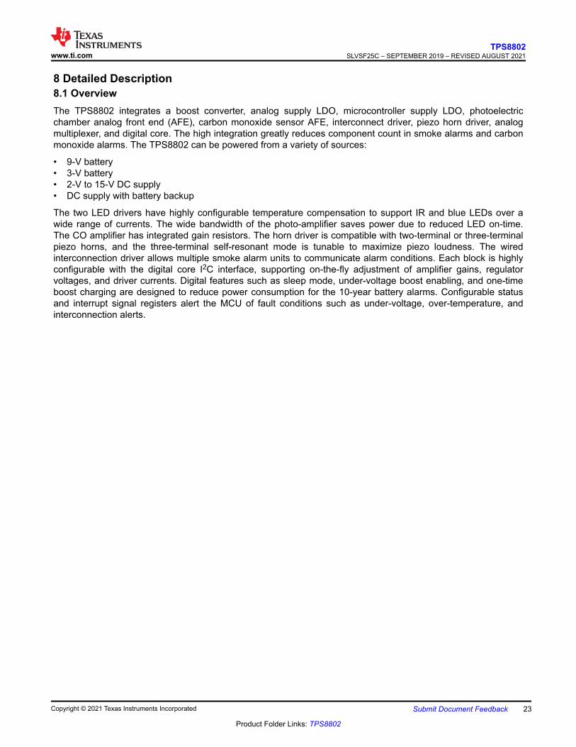
7 Typical Characteristics................................................. 228 Detailed Description......................................................23
8.1 Overview................................................................... 238.2 Functional Block Diagram......................................... 248.3 Feature Description...................................................25
8.4 Device Functional Modes..........................................408.5 Programming............................................................ 428.6 Register Maps...........................................................42
9 Application and Implementation.................................. 549.1 Application Information............................................. 549.2 Typical Application.................................................... 55
10 Power Supply Recommendations..............................6211 Layout...........................................................................63
11.1 Layout Guidelines................................................... 6311.2 Layout Example...................................................... 64
12 Device and Documentation Support..........................6812.1 Receiving Notification of Documentation Updates..6812.2 Support Resources................................................. 6812.3 Trademarks.............................................................6812.4 Electrostatic Discharge Caution..............................6812.5 Glossary..................................................................68
13 Mechanical, Packaging, and Orderable Information.................................................................... 69
4 Revision HistoryNOTE: Page numbers for previous revisions may differ from page numbers in the current version.
Changes from Revision B (March 2021) to Revision C (August 2021) Page• Updated Figure 3-1 ............................................................................................................................................1• Updated Figure 8-4 ..........................................................................................................................................29• Added Connect a capacitor with a value between 1 µF and 100 µF to the LEDLDO. to Section 8.3.4.2 ........30• Updated VCCLOW description in Section 8.6.2 .............................................................................................. 44• Updated Figure 9-1 ..........................................................................................................................................55• Updated Figure 9-10 ........................................................................................................................................59
Changes from Revision A (March 2020) to Revision B (March 2021) Page• Changed typical IMCULDO,Q based on measurement data...................................................................................6• Changed typical ICO,Q based on measurement data.......................................................................................... 6• Added requirement when enabling the boost converter and disabling the photo input amplifier......................33
Changes from Revision * (October 2019) to Revision A (March 2020) Page• Changed document status from Advanced Information to Production Data ......................................................1• Added typical value to VPDIN,OFS ....................................................................................................................... 6• Added typical value to VOFFS,CO ........................................................................................................................ 6• Added typical value to VMUX,OFFS ...................................................................................................................... 6
TPS8802SLVSF25C – SEPTEMBER 2019 – REVISED AUGUST 2021 www.ti.com
2 Submit Document Feedback Copyright © 2021 Texas Instruments Incorporated
Product Folder Links: TPS8802
5 Pin Configuration and Functions
Thermal
Pad
VCC
REF0P3
COP
PREF
CON
AMUX
COO
DGND
HBEN
LEDEN
CSEL
SCL
SDA
GPIO
INT_UNIT
INT_MCU
VMCU
PLDO
VINT
20
38
36
37
35
33
34
32
30
31
29
27
28
26
24
25
23
21
22
VBST
RESERVED
RESERVED
RESERVED
LEDLDO
PDP
AGND
PDN
CSA
PDO
DINA
DINB
CSB
MCUSEL
HORNSL
HORNBR
HORNFB
VLX
PGND
19
1
3
2
4
6
5
7
9
8
10
12
11
13
15
14
16
18
17
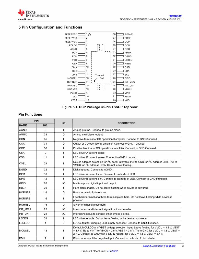
Figure 5-1. DCP Package 38-Pin TSSOP Top View
Pin FunctionsPIN
I/O DESCRIPTIONNAME NO.AGND 5 I Analog ground. Connect to ground plane.
AMUX 33 O Analog multiplexer output.
CON 35 I Negative terminal of CO operational amplifier. Connect to GND if unused.
COO 34 O Output of CO operational amplifier. Connect to GND if unused.
COP 36 I Positive terminal of CO operational amplifier. Connect to GND if unused.
CSA 9 I LED driver A current sense.
CSB 11 I LED driver B current sense. Connect to GND if unused.
CSEL 29 I Device address select pin for I2C serial interface. Pull to GND for I2C address 0x3F. Pull to VMCU for I2C address 0x2A. Do not leave floating.
DGND 32 I Digital ground. Connect to AGND.
DINA 10 I LED driver A current sink. Connect to cathode of LED.
DINB 12 I LED driver B current sink. Connect to cathode of LED. Connect to GND if unused.
GPIO 26 I/O Multi-purpose digital input and output.
HBEN 30 I Horn block enable. Do not leave floating while device is powered.
HORNBR 14 O Brass terminal of piezo horn.
HORNFB 16 I Feedback terminal of a three-terminal piezo horn. Do not leave floating while device is powered.
HORNSL 15 O Silver terminal of piezo horn.
INT_MCU 25 I/O Interconnect and interrupt signal to microcontroller.
INT_UNIT 24 I/O Interconnect bus to connect other smoke alarms.
LEDEN 31 I LED driver enable. Do not leave floating while device is powered.
LEDLDO 4 O LDO output for charging LED supply capacitor. Connect to GND if unused.
MCUSEL 13 IDefault MCULDO and VBST voltage selection input. Leave floating for VMCU = 3.3 V, VBST = 4.7 V. Tie to VINT for VMCU = 2.5 V, VBST = 3.8 V. Tie to GND for VMCU = 1.8 V, VBST = 2.7 V. Connect to GND with a 620-Ω resistor for VMCU = 1.5 V, VBST = 2.7 V.
PDN 7 I Photo input amplifier negative input. Connect to cathode of photodiode.
www.ti.comTPS8802
SLVSF25C – SEPTEMBER 2019 – REVISED AUGUST 2021
Copyright © 2021 Texas Instruments Incorporated Submit Document Feedback 3
Product Folder Links: TPS8802
PINI/O DESCRIPTION
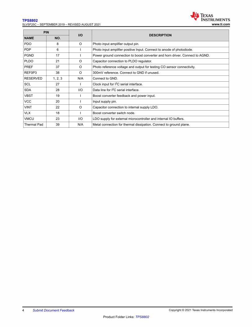
NAME NO.PDO 8 O Photo input amplifier output pin.
PDP 6 I Photo input amplifier positive Input. Connect to anode of photodiode.
PGND 17 I Power ground connection to boost converter and horn driver. Connect to AGND.
PLDO 21 O Capacitor connection to PLDO regulator.
PREF 37 O Photo reference voltage and output for testing CO sensor connectivity.
REF0P3 38 O 300mV reference. Connect to GND if unused.
RESERVED 1, 2, 3 N/A Connect to GND.
SCL 27 I Clock input for I2C serial interface.
SDA 28 I/O Data line for I2C serial interface.
VBST 19 I Boost converter feedback and power input.
VCC 20 I Input supply pin.
VINT 22 O Capacitor connection to internal supply LDO.
VLX 18 I Boost converter switch node.
VMCU 23 I/O LDO supply for external microcontroller and internal IO buffers.
Thermal Pad 39 N/A Metal connection for thermal dissipation. Connect to ground plane.
TPS8802SLVSF25C – SEPTEMBER 2019 – REVISED AUGUST 2021 www.ti.com
4 Submit Document Feedback Copyright © 2021 Texas Instruments Incorporated
Product Folder Links: TPS8802
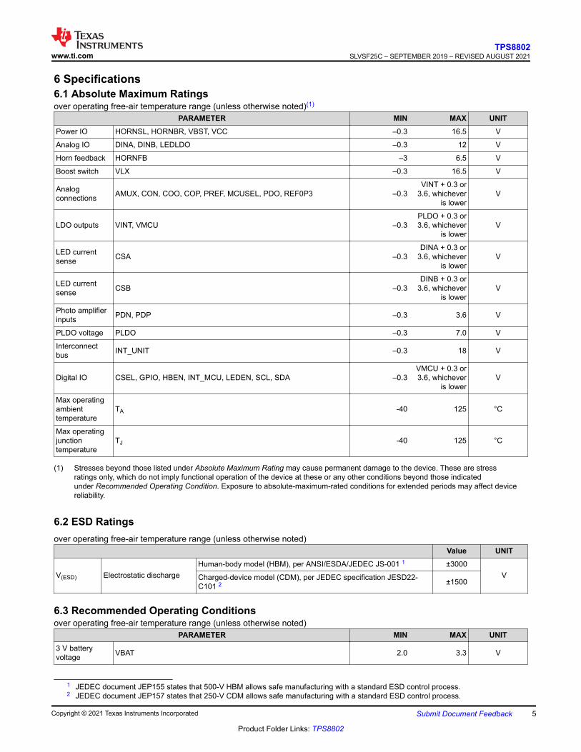
6 Specifications6.1 Absolute Maximum Ratingsover operating free-air temperature range (unless otherwise noted)(1)
PARAMETER MIN MAX UNITPower IO HORNSL, HORNBR, VBST, VCC –0.3 16.5 V
Analog IO DINA, DINB, LEDLDO –0.3 12 V
Horn feedback HORNFB –3 6.5 V
Boost switch VLX –0.3 16.5 V
Analog connections AMUX, CON, COO, COP, PREF, MCUSEL, PDO, REF0P3 –0.3
VINT + 0.3 or 3.6, whichever
is lowerV
LDO outputs VINT, VMCU –0.3PLDO + 0.3 or 3.6, whichever
is lowerV
LED current sense CSA –0.3
DINA + 0.3 or 3.6, whichever
is lowerV
LED current sense CSB –0.3
DINB + 0.3 or 3.6, whichever
is lowerV
Photo amplifier inputs PDN, PDP –0.3 3.6 V
PLDO voltage PLDO –0.3 7.0 V
Interconnect bus INT_UNIT –0.3 18 V
Digital IO CSEL, GPIO, HBEN, INT_MCU, LEDEN, SCL, SDA –0.3VMCU + 0.3 or 3.6, whichever
is lowerV
Max operating ambient temperature
TA -40 125 °C
Max operating junction temperature
TJ -40 125 °C
(1) Stresses beyond those listed under Absolute Maximum Rating may cause permanent damage to the device. These are stress ratings only, which do not imply functional operation of the device at these or any other conditions beyond those indicated under Recommended Operating Condition. Exposure to absolute-maximum-rated conditions for extended periods may affect device reliability.
6.2 ESD Ratingsover operating free-air temperature range (unless otherwise noted)
Value UNIT
V(ESD) Electrostatic dischargeHuman-body model (HBM), per ANSI/ESDA/JEDEC JS-001 1 ±3000
VCharged-device model (CDM), per JEDEC specification JESD22-C101 2 ±1500
6.3 Recommended Operating Conditionsover operating free-air temperature range (unless otherwise noted)
PARAMETER MIN MAX UNIT3 V battery voltage VBAT 2.0 3.3 V
1 JEDEC document JEP155 states that 500-V HBM allows safe manufacturing with a standard ESD control process.2 JEDEC document JEP157 states that 250-V CDM allows safe manufacturing with a standard ESD control process.
www.ti.comTPS8802
SLVSF25C – SEPTEMBER 2019 – REVISED AUGUST 2021
Copyright © 2021 Texas Instruments Incorporated Submit Document Feedback 5
Product Folder Links: TPS8802
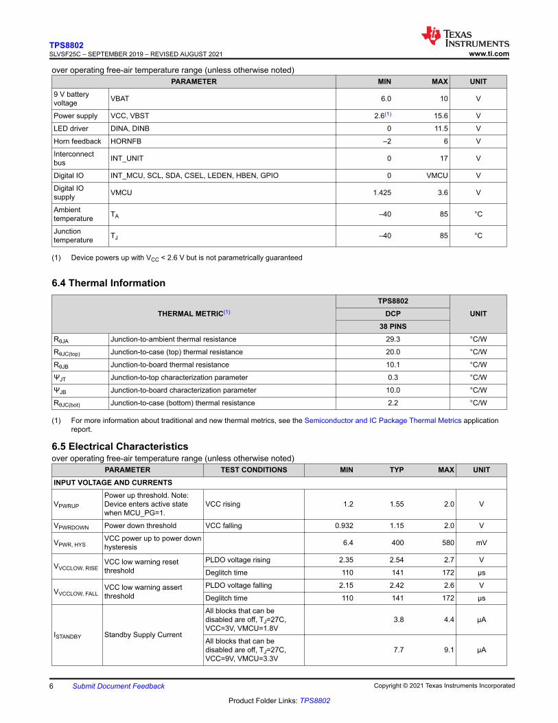
over operating free-air temperature range (unless otherwise noted)PARAMETER MIN MAX UNIT
9 V battery voltage VBAT 6.0 10 V
Power supply VCC, VBST 2.6(1) 15.6 V
LED driver DINA, DINB 0 11.5 V
Horn feedback HORNFB –2 6 V
Interconnect bus INT_UNIT 0 17 V
Digital IO INT_MCU, SCL, SDA, CSEL, LEDEN, HBEN, GPIO 0 VMCU V
Digital IO supply VMCU 1.425 3.6 V
Ambient temperature TA –40 85 °C
Junction temperature TJ –40 85 °C
(1) Device powers up with VCC < 2.6 V but is not parametrically guaranteed
6.4 Thermal Information
THERMAL METRIC(1)
TPS8802UNITDCP
38 PINSRθJA Junction-to-ambient thermal resistance 29.3 °C/W
RθJC(top) Junction-to-case (top) thermal resistance 20.0 °C/W
RθJB Junction-to-board thermal resistance 10.1 °C/W
ΨJT Junction-to-top characterization parameter 0.3 °C/W
ΨJB Junction-to-board characterization parameter 10.0 °C/W
RθJC(bot) Junction-to-case (bottom) thermal resistance 2.2 °C/W
(1) For more information about traditional and new thermal metrics, see the Semiconductor and IC Package Thermal Metrics application report.
6.5 Electrical Characteristicsover operating free-air temperature range (unless otherwise noted)
PARAMETER TEST CONDITIONS MIN TYP MAX UNITINPUT VOLTAGE AND CURRENTS
VPWRUP
Power up threshold. Note: Device enters active state when MCU_PG=1.
VCC rising 1.2 1.55 2.0 V
VPWRDOWN Power down threshold VCC falling 0.932 1.15 2.0 V
VPWR, HYSVCC power up to power down hysteresis 6.4 400 580 mV
VVCCLOW, RISEVCC low warning reset threshold
PLDO voltage rising 2.35 2.54 2.7 V
Deglitch time 110 141 172 µs
VVCCLOW, FALLVCC low warning assert threshold
PLDO voltage falling 2.15 2.42 2.6 V
Deglitch time 110 141 172 µs
ISTANDBY Standby Supply Current
All blocks that can be disabled are off, TJ=27C, VCC=3V, VMCU=1.8V
3.8 4.4 µA
All blocks that can be disabled are off, TJ=27C, VCC=9V, VMCU=3.3V
7.7 9.1 µA
TPS8802SLVSF25C – SEPTEMBER 2019 – REVISED AUGUST 2021 www.ti.com
6 Submit Document Feedback Copyright © 2021 Texas Instruments Incorporated
Product Folder Links: TPS8802
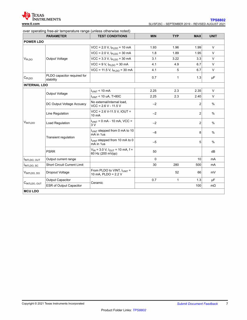
over operating free-air temperature range (unless otherwise noted)PARAMETER TEST CONDITIONS MIN TYP MAX UNIT
POWER LDO
VPLDO Output Voltage
VCC = 2.0 V, IPLDO = 10 mA 1.93 1.96 1.99 V
VCC = 2.0 V, IPLDO = 30 mA 1.8 1.89 1.95 V
VCC = 3.3 V, IPLDO = 30 mA 3.1 3.22 3.3 V
VCC = 9 V, IPLDO = 30 mA 4.1 4.9 6.7 V
VCC = 11.5 V, IPLDO = 30 mA 4.1 5 6.7 V
CPLDOPLDO capacitor required for stability 0.7 1 1.3 µF
INTERNAL LDO
VINTLDO
Output VoltageIVINT < 10 mA 2.25 2.3 2.35 V
IVINT < 10 uA, T>80C 2.25 2.3 2.40 V
DC Output Voltage Accuacy No external/internal load, VCC = 2.6 V - 11.5 V –2 2 %
Line Regulation VCC = 2.6 V-11.5 V, IOUT = 10 mA –2 2 %
Load Regulation IVINT = 0 mA - 10 mA, VCC = 3 V –2 2 %
Transient regulation
IVINT stepped from 0 mA to 10 mA in 1us –8 8 %
IVINT stepped from 10 mA to 0 mA in 1us –5 5 %
PSRR VIN = 3.0 V, IOUT = 10 mA, f = 60 Hz (200 mVpp) 50 dB
IINTLDO, OUT Output current range 0 10 mA
IINTLDO, SC Short Circuit Current Limit 30 280 500 mA
VINTLDO, DO Dropout Voltage From PLDO to VINT, IVINT = 10 mA, PLDO = 2.2 V 52 66 mV
CINTLDO, OUTOutput Capacitor
Ceramic0.7 1 1.3 µF
ESR of Output Capacitor 100 mΩ
MCU LDO
www.ti.comTPS8802
SLVSF25C – SEPTEMBER 2019 – REVISED AUGUST 2021
Copyright © 2021 Texas Instruments Incorporated Submit Document Feedback 7
Product Folder Links: TPS8802
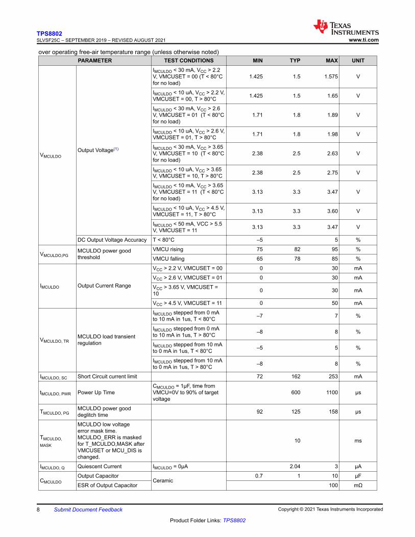
over operating free-air temperature range (unless otherwise noted)PARAMETER TEST CONDITIONS MIN TYP MAX UNIT
VMCULDOOutput Voltage(1)
IMCULDO < 30 mA, VCC > 2.2 V, VMCUSET = 00 (T < 80°C for no load)
1.425 1.5 1.575 V
IMCULDO < 10 uA, VCC > 2.2 V, VMCUSET = 00, T > 80°C 1.425 1.5 1.65 V
IMCULDO < 30 mA, VCC > 2.6 V, VMCUSET = 01 (T < 80°C for no load)
1.71 1.8 1.89 V
IMCULDO < 10 uA, VCC > 2.6 V, VMCUSET = 01, T > 80°C 1.71 1.8 1.98 V
IMCULDO < 30 mA, VCC > 3.65 V, VMCUSET = 10 (T < 80°C for no load)
2.38 2.5 2.63 V
IMCULDO < 10 uA, VCC > 3.65 V, VMCUSET = 10, T > 80°C 2.38 2.5 2.75 V
IMCULDO < 10 mA, VCC > 3.65 V, VMCUSET = 11 (T < 80°C for no load)
3.13 3.3 3.47 V
IMCULDO < 10 uA, VCC > 4.5 V, VMCUSET = 11, T > 80°C 3.13 3.3 3.60 V
IMCULDO < 50 mA, VCC > 5.5 V, VMCUSET = 11 3.13 3.3 3.47 V
DC Output Voltage Accuracy T < 80°C –5 5 %
VMCULDO,PGMCULDO power good threshold
VMCU rising 75 82 95 %
VMCU falling 65 78 85 %
IMCULDO Output Current Range
VCC > 2.2 V, VMCUSET = 00 0 30 mA
VCC > 2.6 V, VMCUSET = 01 0 30 mA
VCC > 3.65 V, VMCUSET = 10 0 30 mA
VCC > 4.5 V, VMCUSET = 11 0 50 mA
VMCULDO, TRMCULDO load transient regulation
IMCULDO stepped from 0 mA to 10 mA in 1us, T < 80°C –7 7 %
IMCULDO stepped from 0 mA to 10 mA in 1us, T > 80°C –8 8 %
IMCULDO stepped from 10 mA to 0 mA in 1us, T < 80°C –5 5 %
IMCULDO stepped from 10 mA to 0 mA in 1us, T > 80°C –8 8 %
IMCULDO, SC Short Circuit current limit 72 162 253 mA
tMCULDO, PWR Power Up TimeCMCULDO = 1µF, time from VMCU=0V to 90% of target voltage
600 1100 µs
TMCULDO, PGMCULDO power good deglitch time 92 125 158 µs
TMCULDO, MASK
MCULDO low voltage error mask time. MCULDO_ERR is masked for T_MCULDO,MASK after VMCUSET or MCU_DIS is changed.
10 ms
IMCULDO, Q Quiescent Current IMCULDO = 0µA 2.04 3 µA
CMCULDOOutput Capacitor
Ceramic0.7 1 10 µF
ESR of Output Capacitor 100 mΩ
TPS8802SLVSF25C – SEPTEMBER 2019 – REVISED AUGUST 2021 www.ti.com
8 Submit Document Feedback Copyright © 2021 Texas Instruments Incorporated
Product Folder Links: TPS8802
over operating free-air temperature range (unless otherwise noted)PARAMETER TEST CONDITIONS MIN TYP MAX UNIT
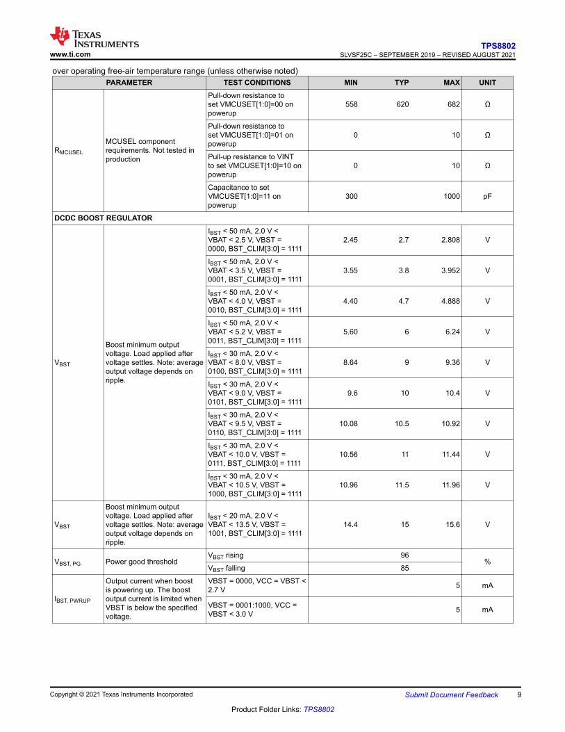
RMCUSEL
MCUSEL component requirements. Not tested in production
Pull-down resistance to set VMCUSET[1:0]=00 on powerup
558 620 682 Ω
Pull-down resistance to set VMCUSET[1:0]=01 on powerup
0 10 Ω
Pull-up resistance to VINT to set VMCUSET[1:0]=10 on powerup
0 10 Ω
Capacitance to set VMCUSET[1:0]=11 on powerup
300 1000 pF
DCDC BOOST REGULATOR
VBST
Boost minimum output voltage. Load applied after voltage settles. Note: average output voltage depends on ripple.
IBST < 50 mA, 2.0 V < VBAT < 2.5 V, VBST = 0000, BST_CLIM[3:0] = 1111
2.45 2.7 2.808 V
IBST < 50 mA, 2.0 V < VBAT < 3.5 V, VBST = 0001, BST_CLIM[3:0] = 1111
3.55 3.8 3.952 V
IBST < 50 mA, 2.0 V < VBAT < 4.0 V, VBST = 0010, BST_CLIM[3:0] = 1111
4.40 4.7 4.888 V
IBST < 50 mA, 2.0 V < VBAT < 5.2 V, VBST = 0011, BST_CLIM[3:0] = 1111
5.60 6 6.24 V
IBST < 30 mA, 2.0 V < VBAT < 8.0 V, VBST = 0100, BST_CLIM[3:0] = 1111
8.64 9 9.36 V
IBST < 30 mA, 2.0 V < VBAT < 9.0 V, VBST = 0101, BST_CLIM[3:0] = 1111
9.6 10 10.4 V
IBST < 30 mA, 2.0 V < VBAT < 9.5 V, VBST = 0110, BST_CLIM[3:0] = 1111
10.08 10.5 10.92 V
IBST < 30 mA, 2.0 V < VBAT < 10.0 V, VBST = 0111, BST_CLIM[3:0] = 1111
10.56 11 11.44 V
IBST < 30 mA, 2.0 V < VBAT < 10.5 V, VBST = 1000, BST_CLIM[3:0] = 1111
10.96 11.5 11.96 V
VBST
Boost minimum output voltage. Load applied after voltage settles. Note: average output voltage depends on ripple.
IBST < 20 mA, 2.0 V < VBAT < 13.5 V, VBST = 1001, BST_CLIM[3:0] = 1111
14.4 15 15.6 V
VBST, PG Power good thresholdVBST rising 96
%VBST falling 85
IBST, PWRUP
Output current when boost is powering up. The boost output current is limited when VBST is below the specified voltage.
VBST = 0000, VCC = VBST < 2.7 V 5 mA
VBST = 0001:1000, VCC = VBST < 3.0 V 5 mA
www.ti.comTPS8802
SLVSF25C – SEPTEMBER 2019 – REVISED AUGUST 2021
Copyright © 2021 Texas Instruments Incorporated Submit Document Feedback 9
Product Folder Links: TPS8802
over operating free-air temperature range (unless otherwise noted)PARAMETER TEST CONDITIONS MIN TYP MAX UNIT
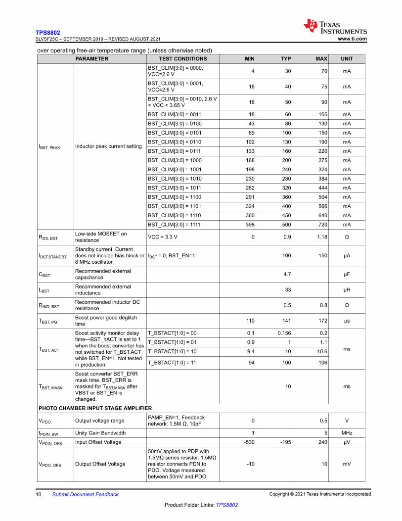
IBST, PEAK Inductor peak current setting
BST_CLIM[3:0] = 0000, VCC=2.6 V 4 30 70 mA
BST_CLIM[3:0] = 0001, VCC=2.6 V 18 40 75 mA
BST_CLIM[3:0] = 0010, 2.6 V < VCC < 3.65 V 18 50 90 mA
BST_CLIM[3:0] = 0011 18 60 105 mA
BST_CLIM[3:0] = 0100 43 80 130 mA
BST_CLIM[3:0] = 0101 69 100 150 mA
BST_CLIM[3:0] = 0110 102 130 190 mA
BST_CLIM[3:0] = 0111 133 160 220 mA
BST_CLIM[3:0] = 1000 168 200 275 mA
BST_CLIM[3:0] = 1001 198 240 324 mA
BST_CLIM[3:0] = 1010 230 280 384 mA
BST_CLIM[3:0] = 1011 262 320 444 mA
BST_CLIM[3:0] = 1100 291 360 504 mA
BST_CLIM[3:0] = 1101 324 400 566 mA
BST_CLIM[3:0] = 1110 360 450 640 mA
BST_CLIM[3:0] = 1111 398 500 720 mA
RDS, BSTLow-side MOSFET on resistance VCC = 3.3 V 0 0.9 1.18 Ω
IBST,STANDBY
Standby current. Current does not include bias block or 8 MHz oscillator.
IBST = 0, BST_EN=1. 100 150 µA
CBSTRecommended external capacitance 4.7 µF
LBSTRecommended external inductance 33 µH
RIND, BSTRecommended inductor DC resistance 0.5 0.8 Ω
TBST, PGBoost power good deglitch time 110 141 172 µs
TBST, ACT
Boost activity monitor delay time—BST_nACT is set to 1 when the boost converter has not switched for T_BST,ACT while BST_EN=1. Not tested in production.
T_BSTACT[1:0] = 00 0.1 0.156 0.2
msT_BSTACT[1:0] = 01 0.9 1 1.1
T_BSTACT[1:0] = 10 9.4 10 10.6
T_BSTACT[1:0] = 11 94 100 106
TBST, MASK
Boost converter BST_ERR mask time. BST_ERR is masked for TBST,MASK after VBST or BST_EN is changed.
10 ms
PHOTO CHAMBER INPUT STAGE AMPLIFIER
VPDO Output voltage range PAMP_EN=1, Feedback network: 1.5M Ω, 10pF 0 0.5 V
fPDIN, BW Unity Gain Bandwidth 1 5 MHz
VPDIN, OFS Input Offset Voltage -530 -195 240 µV
VPDO, OFS Output Offset Voltage
50mV applied to PDP with 1.5MΩ series resistor. 1.5MΩ resistor connects PDN to PDO. Voltage measured between 50mV and PDO.
-10 10 mV
TPS8802SLVSF25C – SEPTEMBER 2019 – REVISED AUGUST 2021 www.ti.com
10 Submit Document Feedback Copyright © 2021 Texas Instruments Incorporated
Product Folder Links: TPS8802
over operating free-air temperature range (unless otherwise noted)PARAMETER TEST CONDITIONS MIN TYP MAX UNIT
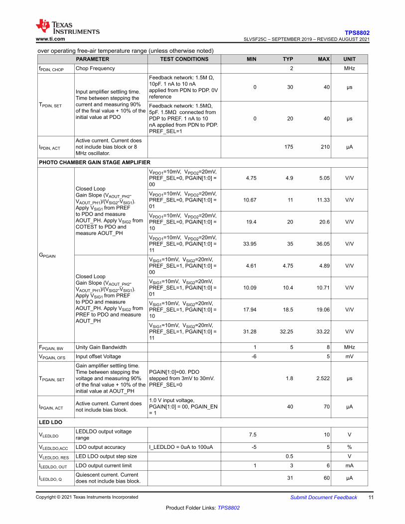
fPDIN, CHOP Chop Frequency 2 MHz
TPDIN, SET
Input amplifier settling time. Time between stepping the current and measuring 90% of the final value + 10% of the initial value at PDO
Feedback network: 1.5M Ω, 10pF. 1 nA to 10 nA applied from PDN to PDP. 0V reference
0 30 40 µs
Feedback network: 1.5MΩ, 5pF. 1.5MΩ connected from PDP to PREF. 1 nA to 10 nA applied from PDN to PDP. PREF_SEL=1
0 20 40 µs
IPDIN, ACT
Active current. Current does not include bias block or 8 MHz oscillator.
175 210 µA
PHOTO CHAMBER GAIN STAGE AMPLIFIER
GPGAIN
Closed Loop Gain Slope (VAOUT_PH2-VAOUT_PH1)/(VSIG2-VSIG1). Apply VSIG1 from PREF to PDO and measure AOUT_PH. Apply VSIG2 from COTEST to PDO and measure AOUT_PH
VPDO1=10mV, VPDO2=20mV, PREF_SEL=0, PGAIN[1:0] = 00
4.75 4.9 5.05 V/V
VPDO1=10mV, VPDO2=20mV, PREF_SEL=0, PGAIN[1:0] = 01
10.67 11 11.33 V/V
VPDO1=10mV, VPDO2=20mV, PREF_SEL=0, PGAIN[1:0] = 10
19.4 20 20.6 V/V
VPDO1=10mV, VPDO2=20mV, PREF_SEL=0, PGAIN[1:0] = 11
33.95 35 36.05 V/V
Closed Loop Gain Slope (VAOUT_PH2-VAOUT_PH1)/(VSIG2-VSIG1). Apply VSIG1 from PREF to PDO and measure AOUT_PH. Apply VSIG2 from PREF to PDO and measure AOUT_PH
VSIG1=10mV, VSIG2=20mV, PREF_SEL=1, PGAIN[1:0] = 00
4.61 4.75 4.89 V/V
VSIG1=10mV, VSIG2=20mV, PREF_SEL=1, PGAIN[1:0] = 01
10.09 10.4 10.71 V/V
VSIG1=10mV, VSIG2=20mV, PREF_SEL=1, PGAIN[1:0] = 10
17.94 18.5 19.06 V/V
VSIG1=10mV, VSIG2=20mV, PREF_SEL=1, PGAIN[1:0] = 11
31.28 32.25 33.22 V/V
FPGAIN, BW Unity Gain Bandwidth 1 5 8 MHz
VPGAIN, OFS Input offset Voltage -6 5 mV
TPGAIN, SET
Gain amplifier settling time. Time between stepping the voltage and measuring 90% of the final value + 10% of the initial value at AOUT_PH
PGAIN[1:0]=00. PDO stepped from 3mV to 30mV. PREF_SEL=0
1.8 2.522 µs
IPGAIN, ACTActive current. Current does not include bias block.
1.0 V input voltage, PGAIN[1:0] = 00, PGAIN_EN = 1
40 70 µA
LED LDO
VLEDLDOLEDLDO output voltage range 7.5 10 V
VLEDLDO,ACC LDO output accuracy I_LEDLDO = 0uA to 100uA -5 5 %
VLEDLDO, RES LED LDO output step size 0.5 V
ILEDLDO, OUT LDO output current limit 1 3 6 mA
ILEDLDO, QQuiescent current. Current does not include bias block. 31 60 µA
www.ti.comTPS8802
SLVSF25C – SEPTEMBER 2019 – REVISED AUGUST 2021
Copyright © 2021 Texas Instruments Incorporated Submit Document Feedback 11
Product Folder Links: TPS8802
over operating free-air temperature range (unless otherwise noted)PARAMETER TEST CONDITIONS MIN TYP MAX UNIT
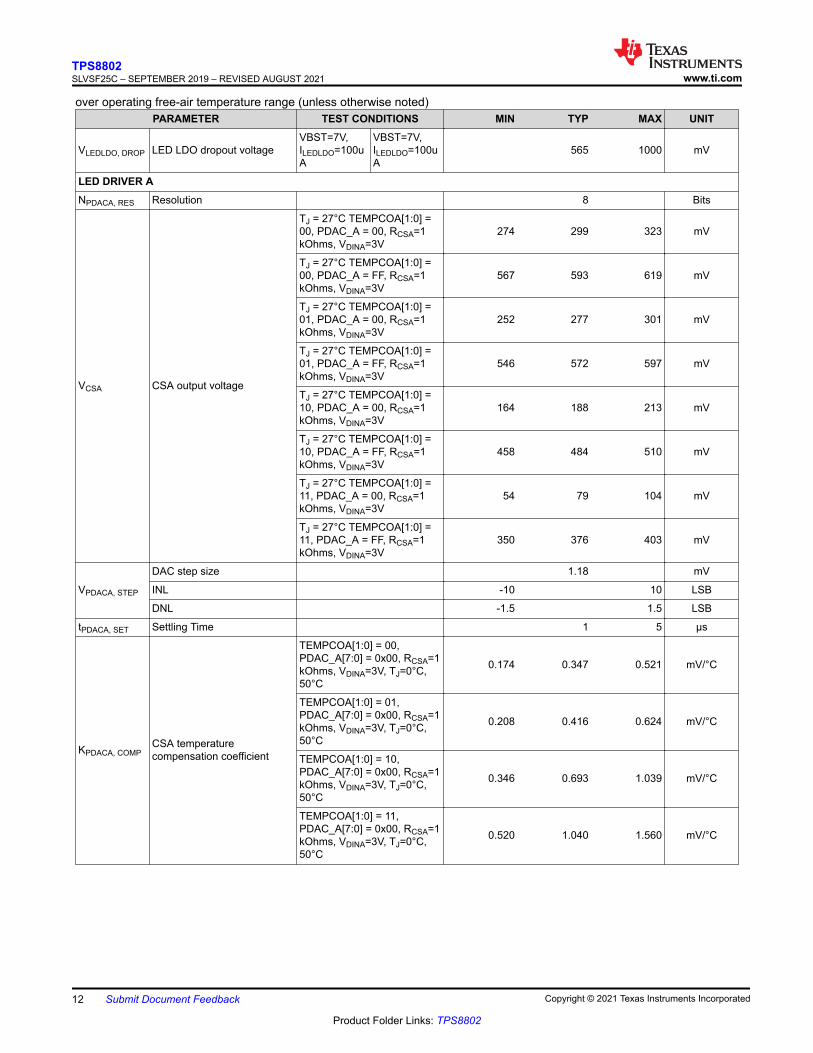
VLEDLDO, DROP LED LDO dropout voltageVBST=7V, ILEDLDO=100uA
VBST=7V, ILEDLDO=100uA
565 1000 mV
LED DRIVER ANPDACA, RES Resolution 8 Bits
VCSA CSA output voltage
TJ = 27°C TEMPCOA[1:0] = 00, PDAC_A = 00, RCSA=1 kOhms, VDINA=3V
274 299 323 mV
TJ = 27°C TEMPCOA[1:0] = 00, PDAC_A = FF, RCSA=1 kOhms, VDINA=3V
567 593 619 mV
TJ = 27°C TEMPCOA[1:0] = 01, PDAC_A = 00, RCSA=1 kOhms, VDINA=3V
252 277 301 mV
TJ = 27°C TEMPCOA[1:0] = 01, PDAC_A = FF, RCSA=1 kOhms, VDINA=3V
546 572 597 mV
TJ = 27°C TEMPCOA[1:0] = 10, PDAC_A = 00, RCSA=1 kOhms, VDINA=3V
164 188 213 mV
TJ = 27°C TEMPCOA[1:0] = 10, PDAC_A = FF, RCSA=1 kOhms, VDINA=3V
458 484 510 mV
TJ = 27°C TEMPCOA[1:0] = 11, PDAC_A = 00, RCSA=1 kOhms, VDINA=3V
54 79 104 mV
TJ = 27°C TEMPCOA[1:0] = 11, PDAC_A = FF, RCSA=1 kOhms, VDINA=3V
350 376 403 mV
VPDACA, STEP
DAC step size 1.18 mV
INL -10 10 LSB
DNL -1.5 1.5 LSB
tPDACA, SET Settling Time 1 5 µs
KPDACA, COMPCSA temperature compensation coefficient
TEMPCOA[1:0] = 00, PDAC_A[7:0] = 0x00, RCSA=1 kOhms, VDINA=3V, TJ=0°C, 50°C
0.174 0.347 0.521 mV/°C
TEMPCOA[1:0] = 01, PDAC_A[7:0] = 0x00, RCSA=1 kOhms, VDINA=3V, TJ=0°C, 50°C
0.208 0.416 0.624 mV/°C
TEMPCOA[1:0] = 10, PDAC_A[7:0] = 0x00, RCSA=1 kOhms, VDINA=3V, TJ=0°C, 50°C
0.346 0.693 1.039 mV/°C
TEMPCOA[1:0] = 11, PDAC_A[7:0] = 0x00, RCSA=1 kOhms, VDINA=3V, TJ=0°C, 50°C
0.520 1.040 1.560 mV/°C
TPS8802SLVSF25C – SEPTEMBER 2019 – REVISED AUGUST 2021 www.ti.com
12 Submit Document Feedback Copyright © 2021 Texas Instruments Incorporated
Product Folder Links: TPS8802
over operating free-air temperature range (unless otherwise noted)PARAMETER TEST CONDITIONS MIN TYP MAX UNIT
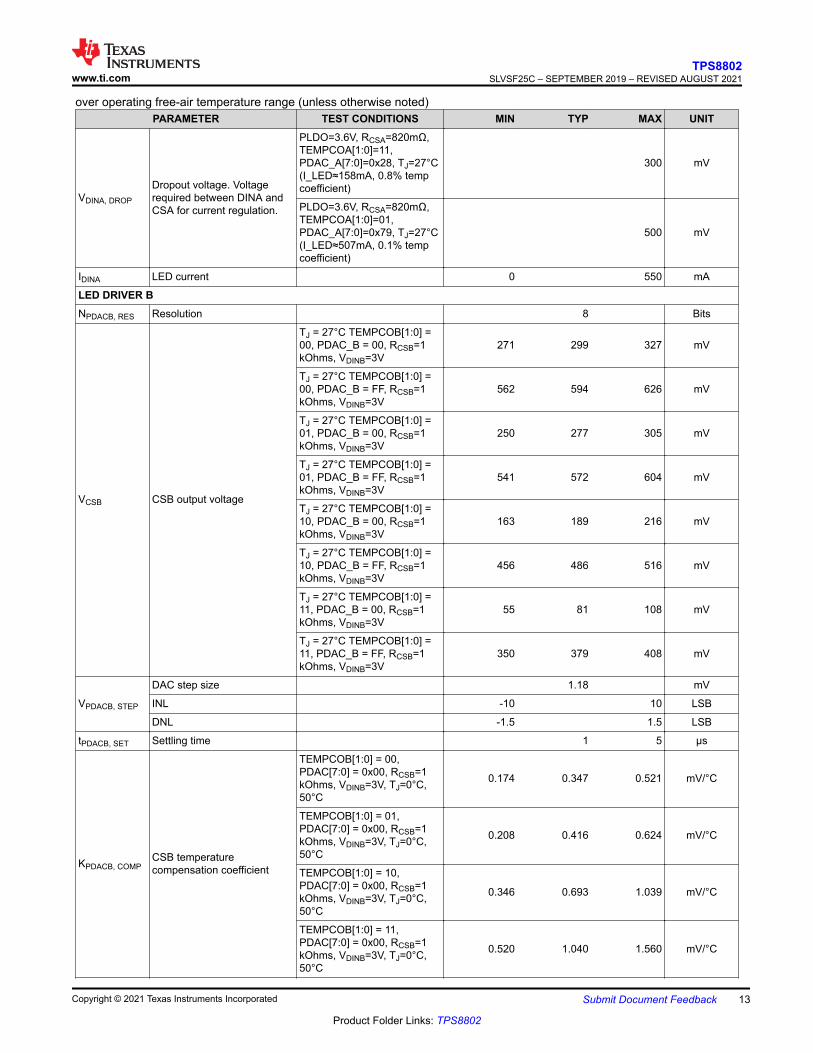
VDINA, DROP
Dropout voltage. Voltage required between DINA and CSA for current regulation.
PLDO=3.6V, RCSA=820mΩ, TEMPCOA[1:0]=11, PDAC_A[7:0]=0x28, TJ=27°C (I_LED≈158mA, 0.8% temp coefficient)
300 mV
PLDO=3.6V, RCSA=820mΩ, TEMPCOA[1:0]=01, PDAC_A[7:0]=0x79, TJ=27°C (I_LED≈507mA, 0.1% temp coefficient)
500 mV
IDINA LED current 0 550 mA
LED DRIVER BNPDACB, RES Resolution 8 Bits
VCSB CSB output voltage
TJ = 27°C TEMPCOB[1:0] = 00, PDAC_B = 00, RCSB=1 kOhms, VDINB=3V
271 299 327 mV
TJ = 27°C TEMPCOB[1:0] = 00, PDAC_B = FF, RCSB=1 kOhms, VDINB=3V
562 594 626 mV
TJ = 27°C TEMPCOB[1:0] = 01, PDAC_B = 00, RCSB=1 kOhms, VDINB=3V
250 277 305 mV
TJ = 27°C TEMPCOB[1:0] = 01, PDAC_B = FF, RCSB=1 kOhms, VDINB=3V
541 572 604 mV
TJ = 27°C TEMPCOB[1:0] = 10, PDAC_B = 00, RCSB=1 kOhms, VDINB=3V
163 189 216 mV
TJ = 27°C TEMPCOB[1:0] = 10, PDAC_B = FF, RCSB=1 kOhms, VDINB=3V
456 486 516 mV
TJ = 27°C TEMPCOB[1:0] = 11, PDAC_B = 00, RCSB=1 kOhms, VDINB=3V
55 81 108 mV
TJ = 27°C TEMPCOB[1:0] = 11, PDAC_B = FF, RCSB=1 kOhms, VDINB=3V
350 379 408 mV
VPDACB, STEP
DAC step size 1.18 mV
INL -10 10 LSB
DNL -1.5 1.5 LSB
tPDACB, SET Settling time 1 5 µs
KPDACB, COMPCSB temperature compensation coefficient
TEMPCOB[1:0] = 00, PDAC[7:0] = 0x00, RCSB=1 kOhms, VDINB=3V, TJ=0°C, 50°C
0.174 0.347 0.521 mV/°C
TEMPCOB[1:0] = 01, PDAC[7:0] = 0x00, RCSB=1 kOhms, VDINB=3V, TJ=0°C, 50°C
0.208 0.416 0.624 mV/°C
TEMPCOB[1:0] = 10, PDAC[7:0] = 0x00, RCSB=1 kOhms, VDINB=3V, TJ=0°C, 50°C
0.346 0.693 1.039 mV/°C
TEMPCOB[1:0] = 11, PDAC[7:0] = 0x00, RCSB=1 kOhms, VDINB=3V, TJ=0°C, 50°C
0.520 1.040 1.560 mV/°C
www.ti.comTPS8802
SLVSF25C – SEPTEMBER 2019 – REVISED AUGUST 2021
Copyright © 2021 Texas Instruments Incorporated Submit Document Feedback 13
Product Folder Links: TPS8802
over operating free-air temperature range (unless otherwise noted)PARAMETER TEST CONDITIONS MIN TYP MAX UNIT
VDINB, DROP
Dropout voltage. Voltage required between DINB and CSB for current regulation.
PLDO=3.6V, RCSA=820mΩ, TEMPCOB[1:0]=11, PDAC[7:0]=0x28, TJ=27°C (I_LED≈158mA, 0.8% temp coefficient)
300 mV
PLDO=3.6V, RCSA=820mΩ, TEMPCOB[1:0]=01, PDAC[7:0]=0x79, TJ=27°C (I_LED≈507mA, 0.1% temp coefficient)
500 mV
IDINB LED current 0 550 mA
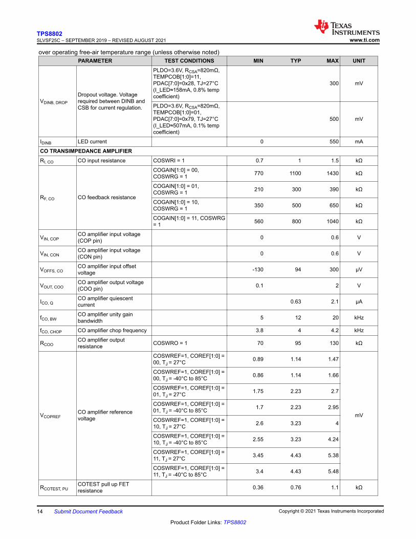
CO TRANSIMPEDANCE AMPLIFIERRI, CO CO input resistance COSWRI = 1 0.7 1 1.5 kΩ
RF, CO CO feedback resistance
COGAIN[1:0] = 00, COSWRG = 1 770 1100 1430 kΩ
COGAIN[1:0] = 01, COSWRG = 1 210 300 390 kΩ
COGAIN[1:0] = 10, COSWRG = 1 350 500 650 kΩ
COGAIN[1:0] = 11, COSWRG = 1 560 800 1040 kΩ
VIN, COPCO amplifier input voltage (COP pin) 0 0.6 V
VIN, CONCO amplifier input voltage (CON pin) 0 0.6 V
VOFFS, COCO amplifier input offset voltage -130 94 300 µV
VOUT, COOCO amplifier output voltage (COO pin) 0.1 2 V
ICO, QCO amplifier quiescent current 0.63 2.1 µA
fCO, BWCO amplifier unity gain bandwidth 5 12 20 kHz
fCO, CHOP CO amplifier chop frequency 3.8 4 4.2 kHz
RCOOCO amplifier output resistance COSWRO = 1 70 95 130 kΩ
VCOPREFCO amplifier reference voltage
COSWREF=1, COREF[1:0] = 00, TJ = 27°C 0.89 1.14 1.47
mV
COSWREF=1, COREF[1:0] = 00, TJ = -40°C to 85°C 0.86 1.14 1.66
COSWREF=1, COREF[1:0] = 01, TJ = 27°C 1.75 2.23 2.7
COSWREF=1, COREF[1:0] = 01, TJ = -40°C to 85°C 1.7 2.23 2.95
COSWREF=1, COREF[1:0] = 10, TJ = 27°C 2.6 3.23 4
COSWREF=1, COREF[1:0] = 10, TJ = -40°C to 85°C 2.55 3.23 4.24
COSWREF=1, COREF[1:0] = 11, TJ = 27°C 3.45 4.43 5.38
COSWREF=1, COREF[1:0] = 11, TJ = -40°C to 85°C 3.4 4.43 5.48
RCOTEST, PUCOTEST pull up FET resistance 0.36 0.76 1.1 kΩ
TPS8802SLVSF25C – SEPTEMBER 2019 – REVISED AUGUST 2021 www.ti.com
14 Submit Document Feedback Copyright © 2021 Texas Instruments Incorporated
Product Folder Links: TPS8802
over operating free-air temperature range (unless otherwise noted)PARAMETER TEST CONDITIONS MIN TYP MAX UNIT
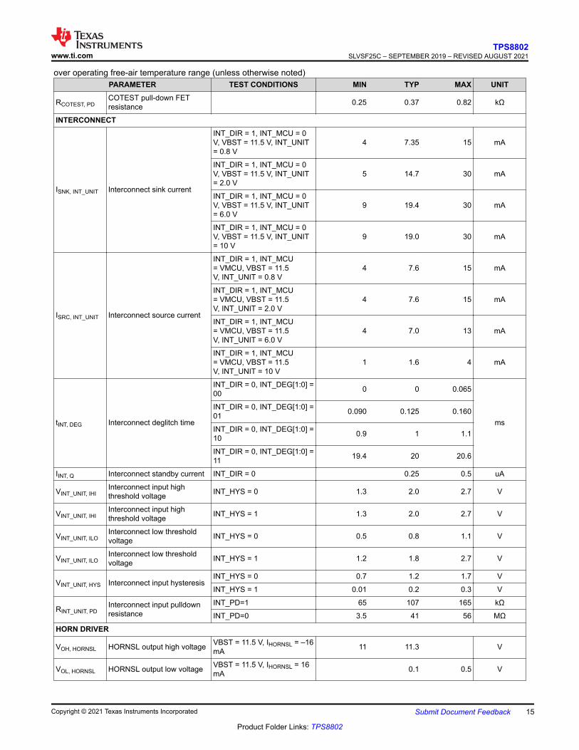
RCOTEST, PDCOTEST pull-down FET resistance 0.25 0.37 0.82 kΩ
INTERCONNECT
ISNK, INT_UNIT Interconnect sink current
INT_DIR = 1, INT_MCU = 0 V, VBST = 11.5 V, INT_UNIT = 0.8 V
4 7.35 15 mA
INT_DIR = 1, INT_MCU = 0 V, VBST = 11.5 V, INT_UNIT = 2.0 V
5 14.7 30 mA
INT_DIR = 1, INT_MCU = 0 V, VBST = 11.5 V, INT_UNIT = 6.0 V
9 19.4 30 mA
INT_DIR = 1, INT_MCU = 0 V, VBST = 11.5 V, INT_UNIT = 10 V
9 19.0 30 mA
ISRC, INT_UNIT Interconnect source current
INT_DIR = 1, INT_MCU = VMCU, VBST = 11.5 V, INT_UNIT = 0.8 V
4 7.6 15 mA
INT_DIR = 1, INT_MCU = VMCU, VBST = 11.5 V, INT_UNIT = 2.0 V
4 7.6 15 mA
INT_DIR = 1, INT_MCU = VMCU, VBST = 11.5 V, INT_UNIT = 6.0 V
4 7.0 13 mA
INT_DIR = 1, INT_MCU = VMCU, VBST = 11.5 V, INT_UNIT = 10 V
1 1.6 4 mA
tINT, DEG Interconnect deglitch time
INT_DIR = 0, INT_DEG[1:0] = 00 0 0 0.065
ms
INT_DIR = 0, INT_DEG[1:0] = 01 0.090 0.125 0.160
INT_DIR = 0, INT_DEG[1:0] = 10 0.9 1 1.1
INT_DIR = 0, INT_DEG[1:0] = 11 19.4 20 20.6
IINT, Q Interconnect standby current INT_DIR = 0 0.25 0.5 uA
VINT_UNIT, IHIInterconnect input high threshold voltage INT_HYS = 0 1.3 2.0 2.7 V
VINT_UNIT, IHIInterconnect input high threshold voltage INT_HYS = 1 1.3 2.0 2.7 V
VINT_UNIT, ILOInterconnect low threshold voltage INT_HYS = 0 0.5 0.8 1.1 V
VINT_UNIT, ILOInterconnect low threshold voltage INT_HYS = 1 1.2 1.8 2.7 V
VINT_UNIT, HYS Interconnect input hysteresisINT_HYS = 0 0.7 1.2 1.7 V
INT_HYS = 1 0.01 0.2 0.3 V
RINT_UNIT, PDInterconnect input pulldown resistance
INT_PD=1 65 107 165 kΩ
INT_PD=0 3.5 41 56 MΩ
HORN DRIVER
VOH, HORNSL HORNSL output high voltage VBST = 11.5 V, IHORNSL = –16 mA 11 11.3 V
VOL, HORNSL HORNSL output low voltage VBST = 11.5 V, IHORNSL = 16 mA 0.1 0.5 V
www.ti.comTPS8802
SLVSF25C – SEPTEMBER 2019 – REVISED AUGUST 2021
Copyright © 2021 Texas Instruments Incorporated Submit Document Feedback 15
Product Folder Links: TPS8802
over operating free-air temperature range (unless otherwise noted)PARAMETER TEST CONDITIONS MIN TYP MAX UNIT
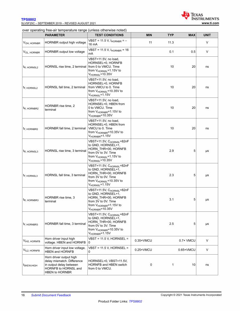
VOH, HORNBR HORNBR output high voltage VBST = 11.5 V, IHORNBR = –16 mA 11 11.3 V
VOL, HORNBR HORNBR output low voltage VBST = 11.5 V, IHORNBR = 16 mA 0.1 0.5 V
tR, HORNSL2 HORNSL rise time, 2 terminal
VBST=11.5V, no load, HORNSEL=0, HORNFB from 0 to VMCU. Time from VHORNSL=1.15V to VHORNSL=10.35V
10 20 ns
tF, HORNSL2 HORNSL fall time, 2 terminal
VBST=11.5V, no load, HORNSEL=0, HORNFB from VMCU to 0. Time from VHORNSL=10.35V to VHORNSL=1.15V
10 20 ns
tR, HORNBR2HORNBR rise time, 2 terminal
VBST=11.5V, no load, HORNSEL=0, HBEN from 0 to VMCU. Time from VHORNBR=1.15V to VHORNBR=10.35V
10 20 ns
tF, HORNBR2 HORNBR fall time, 2 terminal
VBST=11.5V, no load, HORNSEL=0, HBEN from VMCU to 0. Time from VHORNBR=10.35V to VHORNBR=1.15V
10 20 ns
tR, HORNSL3 HORNSL rise time, 3 terminal
VBST=11.5V, CHORNSL=82nF to GND, HORNSEL=1, HORN_THR=00, HORNFB from 0V to 3V. Time from VHORNSL=1.15V to VHORNSL=10.35V
2.9 5 µs
tF, HORNSL3 HORNSL fall time, 3 terminal
VBST=11.5V, CHORNSL=82nF to GND, HORNSEL=1, HORN_THR=00, HORNFB from 3V to 0V. Time from VHORNSL=10.35V to VHORNSL=1.15V
2.3 5 µs
tR, HORNBR3HORNBR rise time, 3 terminal
VBST=11.5V, CHORNSL=82nF to GND, HORNSEL=1, HORN_THR=00, HORNFB from 3V to 0V. Time from VHORNBR=1.15V to VHORNBR=10.35V
3.1 5 µs
tF, HORNBR3 HORNBR fall time, 3 terminal
VBST=11.5V, CHORNSL=82nF to GND, HORNSEL=1, HORN_THR=00, HORNFB from 0V to 3V. Time from VHORNBR=10.35V to VHORNBR=1.15V
2.5 5 µs
VIH2, HORNFBHorn driver input high voltage. HBEN and HORNFB
VBST = 11.5 V, HORNSEL = 0 0.35×VMCU 0.7× VMCU V
VIL2, HORNFBHorn driver input low voltage. HBEN and HORNFB
VBST = 11.5 V, HORNSEL = 0 0.25×VMCU 0.65×VMCU V
tSKEW,HIGH
Horn driver output high delay mismatch. Difference in output delay between HORNFB to HORNSL and HBEN to HORNBR
HORNSEL=0, VBST=11.5V, HORNFB and HBEN switch from 0 to VMCU.
0 1 10 ns
TPS8802SLVSF25C – SEPTEMBER 2019 – REVISED AUGUST 2021 www.ti.com
16 Submit Document Feedback Copyright © 2021 Texas Instruments Incorporated
Product Folder Links: TPS8802
over operating free-air temperature range (unless otherwise noted)PARAMETER TEST CONDITIONS MIN TYP MAX UNIT
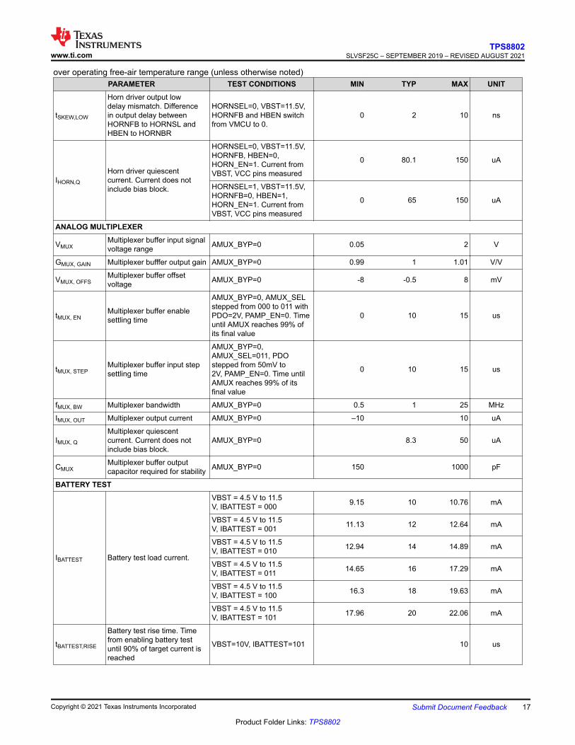
tSKEW,LOW
Horn driver output low delay mismatch. Difference in output delay between HORNFB to HORNSL and HBEN to HORNBR
HORNSEL=0, VBST=11.5V, HORNFB and HBEN switch from VMCU to 0.
0 2 10 ns
IHORN,Q
Horn driver quiescent current. Current does not include bias block.
HORNSEL=0, VBST=11.5V, HORNFB, HBEN=0, HORN_EN=1. Current from VBST, VCC pins measured
0 80.1 150 uA
HORNSEL=1, VBST=11.5V, HORNFB=0, HBEN=1, HORN_EN=1. Current from VBST, VCC pins measured
0 65 150 uA
ANALOG MULTIPLEXER
VMUXMultiplexer buffer input signal voltage range AMUX_BYP=0 0.05 2 V
GMUX, GAIN Multiplexer bufffer output gain AMUX_BYP=0 0.99 1 1.01 V/V
VMUX, OFFSMultiplexer buffer offset voltage AMUX_BYP=0 -8 -0.5 8 mV
tMUX, ENMultiplexer buffer enable settling time
AMUX_BYP=0, AMUX_SEL stepped from 000 to 011 with PDO=2V, PAMP_EN=0. Time until AMUX reaches 99% of its final value
0 10 15 us
tMUX, STEPMultiplexer buffer input step settling time
AMUX_BYP=0, AMUX_SEL=011, PDO stepped from 50mV to 2V, PAMP_EN=0. Time until AMUX reaches 99% of its final value
0 10 15 us
fMUX, BW Multiplexer bandwidth AMUX_BYP=0 0.5 1 25 MHz
IMUX, OUT Multiplexer output current AMUX_BYP=0 –10 10 uA
IMUX, Q
Multiplexer quiescent current. Current does not include bias block.
AMUX_BYP=0 8.3 50 uA
CMUXMultiplexer buffer output capacitor required for stability AMUX_BYP=0 150 1000 pF
BATTERY TEST
IBATTEST Battery test load current.
VBST = 4.5 V to 11.5 V, IBATTEST = 000 9.15 10 10.76 mA
VBST = 4.5 V to 11.5 V, IBATTEST = 001 11.13 12 12.64 mA
VBST = 4.5 V to 11.5 V, IBATTEST = 010 12.94 14 14.89 mA
VBST = 4.5 V to 11.5 V, IBATTEST = 011 14.65 16 17.29 mA
VBST = 4.5 V to 11.5 V, IBATTEST = 100 16.3 18 19.63 mA
VBST = 4.5 V to 11.5 V, IBATTEST = 101 17.96 20 22.06 mA
tBATTEST,RISE
Battery test rise time. Time from enabling battery test until 90% of target current is reached
VBST=10V, IBATTEST=101 10 us
www.ti.comTPS8802
SLVSF25C – SEPTEMBER 2019 – REVISED AUGUST 2021
Copyright © 2021 Texas Instruments Incorporated Submit Document Feedback 17
Product Folder Links: TPS8802
over operating free-air temperature range (unless otherwise noted)PARAMETER TEST CONDITIONS MIN TYP MAX UNIT
tBATTEST,FALL
Battery test fall time. Time from disabling battery test until 10% of initial current is reached
VBST=10V, IBATTEST=101 10 us
OSCILLATOR, REFERENCE SYSTEM
fOSC8Oscillator frequency 8 MHz
Frequency accuracy TA = -10°C to 70°C –3 3 %
fOSC32
Low-power Oscillator frequency 32 kHz
Frequency accuracy TA = -10°C to 70°C –3 3 %
TTIMEOUT Error timeout time 0.9 1 1.1 s
IREF0P3, QREF0P3 buffer quiescent current
VCC current difference between REF0P3_EN=0 and REF0P3=1. IREF0P3=0 µA
0.38 0.76 µA
CREF0P3REF0P3 output capacitor required for stability 0.7 1 1.5 nF
TREF0P3, SET REF0P3 settling timeFrom REF0P3 enabled to 99% of final output voltage. CREF0P3=1nF, IREF0P3=0 µA
1 1.8 ms
VREF0P3, OUT REF0P3 output voltageIREF0P3 = 10 µA 270 300 330 mV
IREF0P3 = -25 µA 270 300 330 mV
IVCCLOW,QVCC_LOW monitor quiescent current 0.9 2 uA
IO BUFFERS
VIO, ILO IO buffer input low threshold LEDEN, CSEL, INT_MCU, GPIO 0.3×VMCU 0.7× VMCU V
VIO, IHI IO buffer input high threshold LEDEN, CSEL, INT_MCU, GPIO 0.3×VMCU 0.7× VMCU V
IIO, LEAKIO buffer input leakage current
LEDEN 100 nA
HBEN 100 nA
CSEL 100 nA
VIO, OL IO buffer output low-level
INT_MCU, GPIO. IIO = 3 mA, VMCU = 1.8 V 0 0.19 0.6 V
INT_MCU, GPIO. IIO = 1 mA, VMCU = 1.5 V 0 0.20 0.6 V
VIO, OH
IO buffer output high-level. Spec is the voltage drop from VMCU (i.e. VMCU - VOH)
INT_MCU, GPIO. IIO = -3 mA, VMCU = 1.8 V 0 0.30 0.6 V
INT_MCU, GPIO. IIO = -1 mA, VMCU = 1.5 V 0 0.37 0.6 V
CIN, IO Input capacitance
LEDEN, CSEL 2 10 pF
HBEN 2 10 pF
INT_MCU, GPIO 2 10 pF
RIO,PDIO buffer input pulldown resistor INT_MCU, GPIO 0.8 10 50 MΩ
THERMAL WARNINGTWARNING Thermal trip point 110 C
THERMAL SHUTDOWN
TSHTDWNThermal trip point 125
CThermal hysteresis 5 15 20
TPS8802SLVSF25C – SEPTEMBER 2019 – REVISED AUGUST 2021 www.ti.com
18 Submit Document Feedback Copyright © 2021 Texas Instruments Incorporated
Product Folder Links: TPS8802
over operating free-air temperature range (unless otherwise noted)PARAMETER TEST CONDITIONS MIN TYP MAX UNIT
tOTS,MASK
Thermal error mask time. OTS_ERR is masked for tOTS,MASK after device fully powers up or OTS_EN set to 1
300 350 us
I2C IOVI2C,IL Low-level input voltage -0.5 0.3 × VMCU V
VI2C,IH High-level input voltage 0.7 × VMCU V
VI2C,HYSHysteresis of Schmitt triggerinputs 0.05 × VMCU V
VI2C,OL Low-level output voltage
3 mA sink current; VMCU >2V 0 0.4 V
2 mA sink current; VMCU < 2V 0 0.2 × VMCU V
II2C,OL Low-level output currentVOL = 0.4 V 2.5 mA
VOL = 0.6 V 4 mA
II2C,IN Input current to each I/O pin 0.1VMCU < VI < 0.9VMCUmax -10 10 µA
CI2C,IN Capacitance for each I/O pin 10 pF
tI2C,OF Output fall time
From VIHmin to VILmax, Standard-Mode 250 ns
From VIHmin to VILmax, Fast-Mode 250 ns
tI2C,SP
Pulse width of spikes that must be suppressed by the input filter
0 50 ns
I2C BUS LINES
fSCL
SCL clock frequency, Standard-Mode 0 100 kHz
SCL clock frequency Fast-Mode 0 400 kHz
tHD;STA
hold time (repeated) START condition, Standard-Mode
After this period, the first clock pulse is generated. 4 µs
hold time (repeated) START condition, Fast-Mode
After this period, the first clock pulse is generated. 0.6 µs
tSCL ,LOW
LOW period of the SCL clock, Standard-Mode 4.7 µs
LOW period of the SCL clock, Fast-Mode 1.3 µs
tSCL,HIGH
HIGH period of the SCL clock, Standard-Mode 4 µs
HIGH period of the SCL clock, Fast-Mode 0.6 µs
tSU;STA
set-up time for a repeated START condition, Standard-Mode
4.7 µs
set-up time for a repeated START condition, Fast-Mode 0.6 µs
tHD;DAT data hold time, Standard-Mode
CBUS compatible masters 5 µs
tHD;DAT I2C-bus devices 0 µs
tHD;DAT data hold time, Fast-ModeCBUS compatible masters 0 µs
tHD;DAT I2C-bus devices 0 µs
www.ti.comTPS8802
SLVSF25C – SEPTEMBER 2019 – REVISED AUGUST 2021
Copyright © 2021 Texas Instruments Incorporated Submit Document Feedback 19
Product Folder Links: TPS8802
over operating free-air temperature range (unless otherwise noted)PARAMETER TEST CONDITIONS MIN TYP MAX UNIT
tSU;DAT
data set-up time, Standard-Mode 250 ns
data set-up time, Fast-Mode 100 ns
tI2C,RISE
rise time of both SDA and SCL signals, Standard-Mode 1000 ns
rise time of both SDA and SCL signals, Fast-Mode 20 300 ns
tI2C,FALL
fall time of both SDA and SCL signals, Standard-Mode 300 ns
fall time of both SDA and SCL signals, Fast-Mode 20 × (VMCU /
5.5 V) 300 ns
tSU;STO
set-up time for STOP condition, Standard-Mode 4 µs
set-up time for STOP condition, Fast-Mode 0.6 µs
tBUF
bus free time between a STOP and START condition, Standard-Mode
4.7 µs
bus free time between a STOP and START condition, Fast-Mode
1.3 µs
tVD;DAT
data valid time, Standard-Mode 3.45 µs
data valid time, Fast-Mode 0.9 µs
tVD;ACK
data valid acknowledge time, Standard-Mode 3.45 µs
data valid acknowledge time, Fast-Mode 0.9 µs
CBUS
capacitive load for each bus line, Standard-Mode 400 pF
capacitive load for each bus line, Fast-Mode 250 pF
VNLnoise margin at the LOW level
for each connected device (including hysteresis) 0.1 × VMCU V
VNHnoise margin at the HIGH level
for each connected device (including hysteresis) 0.2 × VMCU V
(1) MCU LDO output voltage on power-up is determined by the MCUSEL pin state.
6.6 Typical CharacteristicsTA = 27°C, VCC = 3.65 V
TPS8802SLVSF25C – SEPTEMBER 2019 – REVISED AUGUST 2021 www.ti.com
20 Submit Document Feedback Copyright © 2021 Texas Instruments Incorporated
Product Folder Links: TPS8802
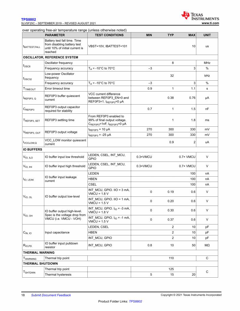
Current (µA)
Co
un
ts
0
5
10
15
20
25
30
35
40
16
2
16
4
16
6
16
8
17
0
17
2
17
4
17
6
17
8
18
0
18
2
1 1 1
5 5
13
16 16
1
µ = 175.41 µA σ = 3.25 µA N = 99 Units
Figure 6-1. 8 MHz Oscillator Current
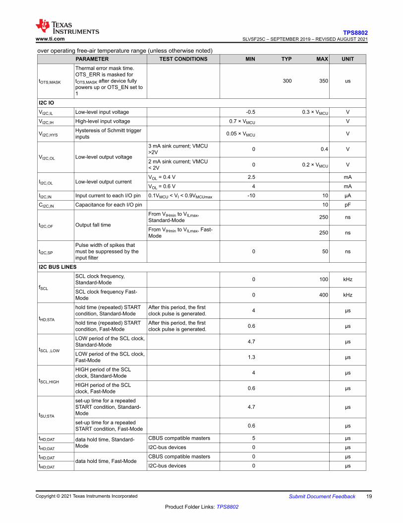
Current (µA)
Co
unts
0
5
10
15
20
25
30
35
60
61
62
63
64
65
66
67
1
10
22
32
26
7
1
µ = 63.44 µA σ = 1.13 µA N = 99 Units
Figure 6-2. Bias Block Current
www.ti.comTPS8802
SLVSF25C – SEPTEMBER 2019 – REVISED AUGUST 2021
Copyright © 2021 Texas Instruments Incorporated Submit Document Feedback 21
Product Folder Links: TPS8802
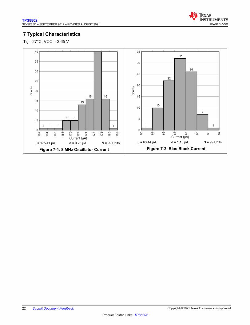
7 Typical CharacteristicsTA = 27°C, VCC = 3.65 V
Current (µA)
Co
un
ts
0
5
10
15
20
25
30
35
40
16
2
16
4
16
6
16
8
17
0
17
2
17
4
17
6
17
8
18
0
18
2
1 1 1
5 5
13
16 16
1
µ = 175.41 µA σ = 3.25 µA N = 99 Units
Figure 7-1. 8 MHz Oscillator Current
Current (µA)C
ou
nts
0
5
10
15
20
25
30
35
60
61
62
63
64
65
66
67
1
10
22
32
26
7
1
µ = 63.44 µA σ = 1.13 µA N = 99 Units
Figure 7-2. Bias Block Current
TPS8802SLVSF25C – SEPTEMBER 2019 – REVISED AUGUST 2021 www.ti.com
22 Submit Document Feedback Copyright © 2021 Texas Instruments Incorporated
Product Folder Links: TPS8802
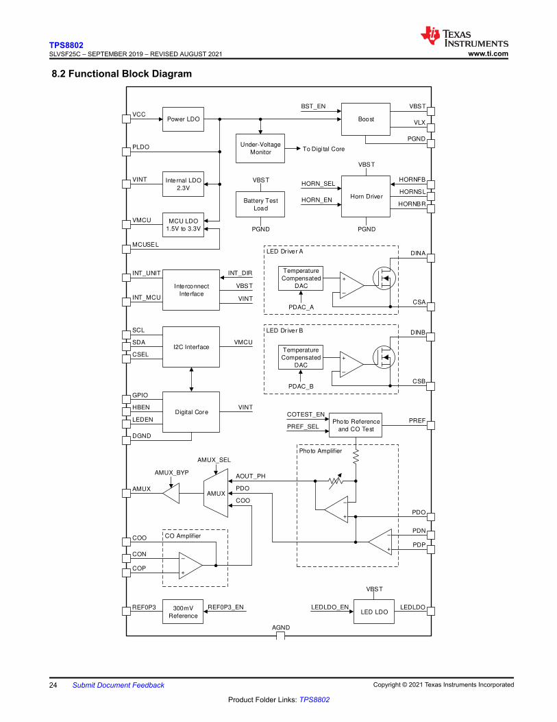
8 Detailed Description8.1 OverviewThe TPS8802 integrates a boost converter, analog supply LDO, microcontroller supply LDO, photoelectric chamber analog front end (AFE), carbon monoxide sensor AFE, interconnect driver, piezo horn driver, analog multiplexer, and digital core. The high integration greatly reduces component count in smoke alarms and carbon monoxide alarms. The TPS8802 can be powered from a variety of sources:
• 9-V battery• 3-V battery• 2-V to 15-V DC supply• DC supply with battery backup
The two LED drivers have highly configurable temperature compensation to support IR and blue LEDs over a wide range of currents. The wide bandwidth of the photo-amplifier saves power due to reduced LED on-time. The CO amplifier has integrated gain resistors. The horn driver is compatible with two-terminal or three-terminal piezo horns, and the three-terminal self-resonant mode is tunable to maximize piezo loudness. The wired interconnection driver allows multiple smoke alarm units to communicate alarm conditions. Each block is highly configurable with the digital core I2C interface, supporting on-the-fly adjustment of amplifier gains, regulator voltages, and driver currents. Digital features such as sleep mode, under-voltage boost enabling, and one-time boost charging are designed to reduce power consumption for the 10-year battery alarms. Configurable status and interrupt signal registers alert the MCU of fault conditions such as under-voltage, over-temperature, and interconnection alerts.
www.ti.comTPS8802
SLVSF25C – SEPTEMBER 2019 – REVISED AUGUST 2021
Copyright © 2021 Texas Instruments Incorporated Submit Document Feedback 23
Product Folder Links: TPS8802
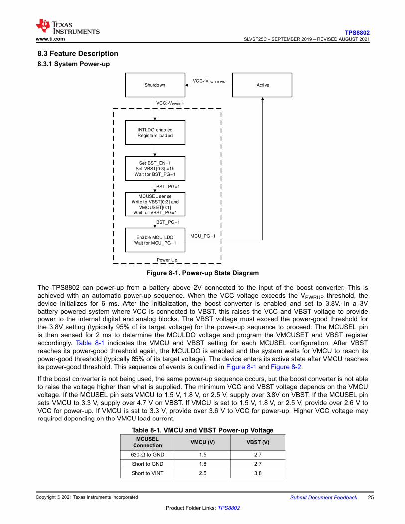
8.2 Functional Block Diagram
LED Dr iver A
CO Amplifier
Photo Amplifier
BoostPower LDO
Internal LDO
2.3V
Under-Voltage
Monitor
MCU LDO
1.5V to 3.3V
MCUSEL
VMCU
VINT
PLDO
VCC
VBST
Photo Reference
and CO Test
+
±
+
±
VLX
Horn Driver
Interconnect
Interface
I2C Interface
INT_UNIT
INT_MCU
SCL
SDA
CSEL
INT_DIR
HORN_SEL
HORN_EN
BST_EN
Digital Core
GPIO
HBEN
LEDEN
DGND
AMUX AMUX
AMUX_BYP AOUT_PH
PDO
COO
+
±
COO
CON
COP
VBST
VINT
HORNFB
HORNSL
HORNBR
AMUX_SEL
VBST
COTEST_EN
PREF_SEL
PGND
PGND
PDP
PDN
PDO
PREF
VMCU
VINT
+
±
Temperature
Compensated
DAC
DINA
CSA
AGND
PDAC_A
Battery Test
Load
PGND
VBST
LED LDO LEDLDO
LED Dr iver B
+
±
Temperature
Compensated
DAC
DINB
CSB PDAC_B
LEDLDO_EN
To Digi tal Core
300mV
Reference
REF0P3 REF0P3_EN
VBST
TPS8802SLVSF25C – SEPTEMBER 2019 – REVISED AUGUST 2021 www.ti.com
24 Submit Document Feedback Copyright © 2021 Texas Instruments Incorporated
Product Folder Links: TPS8802
8.3 Feature Description8.3.1 System Power-up
ActiveShutdown
VCC>VPWRUP
INTLDO enabled
Registers loaded
Set BST_EN=1
Set VBST[0:3] =1h
Wait for BST_PG=1
VCC<VPWRDOWN
MCUSEL sense
Write to VBST[0:3] and
VMCUSET[0:1]
Wait for VBST_PG=1
Enable MCU LDO
Wait for MCU_PG=1
BST_PG=1
BST_PG=1
MCU_PG=1
Power Up
Figure 8-1. Power-up State Diagram
The TPS8802 can power-up from a battery above 2V connected to the input of the boost converter. This is achieved with an automatic power-up sequence. When the VCC voltage exceeds the VPWRUP threshold, the device initializes for 6 ms. After the initialization, the boost converter is enabled and set to 3.8V. In a 3V battery powered system where VCC is connected to VBST, this raises the VCC and VBST voltage to provide power to the internal digital and analog blocks. The VBST voltage must exceed the power-good threshold for the 3.8V setting (typically 95% of its target voltage) for the power-up sequence to proceed. The MCUSEL pin is then sensed for 2 ms to determine the MCULDO voltage and program the VMCUSET and VBST register accordingly. Table 8-1 indicates the VMCU and VBST setting for each MCUSEL configuration. After VBST reaches its power-good threshold again, the MCULDO is enabled and the system waits for VMCU to reach its power-good threshold (typically 85% of its target voltage). The device enters its active state after VMCU reaches its power-good threshold. This sequence of events is outlined in Figure 8-1 and Figure 8-2.
If the boost converter is not being used, the same power-up sequence occurs, but the boost converter is not able to raise the voltage higher than what is supplied. The minimum VCC and VBST voltage depends on the VMCU voltage. If the MCUSEL pin sets VMCU to 1.5 V, 1.8 V, or 2.5 V, supply over 3.8V on VBST. If the MCUSEL pin sets VMCU to 3.3 V, supply over 4.7 V on VBST. If VMCU is set to 1.5 V, 1.8 V, or 2.5 V, provide over 2.6 V to VCC for power-up. If VMCU is set to 3.3 V, provide over 3.6 V to VCC for power-up. Higher VCC voltage may required depending on the VMCU load current.
Table 8-1. VMCU and VBST Power-up VoltageMCUSEL
Connection VMCU (V) VBST (V)
620-Ω to GND 1.5 2.7
Short to GND 1.8 2.7
Short to VINT 2.5 3.8
www.ti.comTPS8802
SLVSF25C – SEPTEMBER 2019 – REVISED AUGUST 2021
Copyright © 2021 Texas Instruments Incorporated Submit Document Feedback 25
Product Folder Links: TPS8802
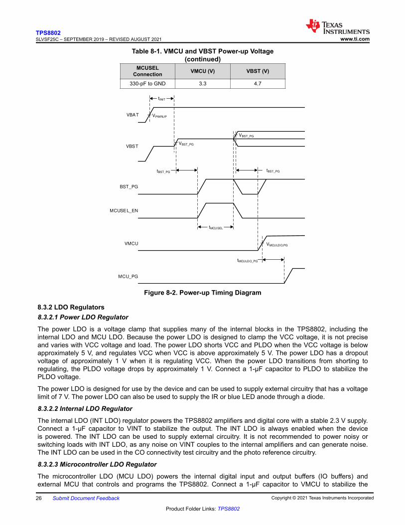
Table 8-1. VMCU and VBST Power-up Voltage (continued)
MCUSEL Connection VMCU (V) VBST (V)
330-pF to GND 3.3 4.7
VBAT
VBST
VPWRUP
tBST_PG
BST_PG
MCUSEL_EN
VBST_PG
tBST_PG
VBST_PG
VMCU
MCU_PG
tMCULDO_PG
VMCULDO,PG
ttMCUSELt
Figure 8-2. Power-up Timing Diagram
8.3.2 LDO Regulators8.3.2.1 Power LDO Regulator
The power LDO is a voltage clamp that supplies many of the internal blocks in the TPS8802, including the internal LDO and MCU LDO. Because the power LDO is designed to clamp the VCC voltage, it is not precise and varies with VCC voltage and load. The power LDO shorts VCC and PLDO when the VCC voltage is below approximately 5 V, and regulates VCC when VCC is above approximately 5 V. The power LDO has a dropout voltage of approximately 1 V when it is regulating VCC. When the power LDO transitions from shorting to regulating, the PLDO voltage drops by approximately 1 V. Connect a 1-µF capacitor to PLDO to stabilize the PLDO voltage.
The power LDO is designed for use by the device and can be used to supply external circuitry that has a voltage limit of 7 V. The power LDO can also be used to supply the IR or blue LED anode through a diode.
8.3.2.2 Internal LDO Regulator
The internal LDO (INT LDO) regulator powers the TPS8802 amplifiers and digital core with a stable 2.3 V supply. Connect a 1-µF capacitor to VINT to stabilize the output. The INT LDO is always enabled when the device is powered. The INT LDO can be used to supply external circuitry. It is not recommended to power noisy or switching loads with INT LDO, as any noise on VINT couples to the internal amplifiers and can generate noise. The INT LDO can be used in the CO connectivity test circuitry and the photo reference circuitry.
8.3.2.3 Microcontroller LDO Regulator
The microcontroller LDO (MCU LDO) powers the internal digital input and output buffers (IO buffers) and external MCU that controls and programs the TPS8802. Connect a 1-µF capacitor to VMCU to stabilize the
TPS8802SLVSF25C – SEPTEMBER 2019 – REVISED AUGUST 2021 www.ti.com
26 Submit Document Feedback Copyright © 2021 Texas Instruments Incorporated
Product Folder Links: TPS8802
output. The MCU LDO can be programmed to output 1.5 V, 1.8 V, 2.5 V, and 3.3 V. The default MCU LDO setting is determined by the configuration on the MCUSEL pin (see Table 8-1). After the device is powered, the MCU LDO voltage can be changed using the VMCUSET register. The MCU LDO can also be disabled using the MCU_DIS register.
The MCU LDO output VMCU powers the IO buffers on SCL, SDA, CSEL, INT_MCU, GPIO, LEDEN, HBEN, and HORNFB. The IO buffers level shift signals from the digital core to a level suitable for the microcontroller and signals from the microcontroller to a level suitable for the digital core. In general, connect VMCU to the microcontroller supply voltage to guarantee logic level compatibility. If the MCU LDO is disabled, connect an external supply to VMCU. This external supply can be a 3-V battery. Connecting a 3-V battery directly to VMCU allows the MCU LDO to be disabled, saving some power in the system. When a 3-V battery is connected to VMCU, set the MCU LDO to 1.5 V or 1.8 V on power-up. The battery voltage overrides the MCU LDO without excess power draw.
The MCU LDO has a power good signal MCU_PG that indicates whether the MCU LDO is above 85% the regulation voltage. A 125-µs deglitch filter prevents noise from affecting the MCU_PG signal. If MCU_PG is low after 10 ms of changing the MCU LDO voltage or enabling the MCU LDO, the MCU_ERR flag is set high. If the MCU_ERR flag is high and MCUERR_DIS is low, the MCU LDO fault state is entered. See Section 8.4.2.1 section for more information.
8.3.3 Photo Chamber AFE
+
±
10 pF
10 pF
Photodiode
To AMUX
+
±
VINT
PREF_SEL
PAMP_EN
PGAIN_EN
To AMUX
PDO
PDN
PDP
PREF
1.5 M
1.5 M
1
0
To CO Amp
Test
VINT
Photo Reference
PGAIN[1:0]
+±
+
±
50mV
5mV
PGAIN_ENPAMP_EN
470 k
VINT
Connect if
PGAIN set to
01, 10, or 11
Figure 8-3. Photo Amplifier Circuit
The TPS8802 photo amplifier connects to a photoelectric chamber photodiode and has two stages—an input stage and gain stage. When the photoelectric chamber LED is enabled, light scatters off smoke particles in the chamber into the photodiode, producing a signal proportional to the smoke concentration. The output of each photo amplifier stage is connected to the AMUX for ADC reading. This configuration provides high bandwidth and dynamic range for the photodiode signal chain as the gain stage is on-the-fly adjustable.
www.ti.comTPS8802
SLVSF25C – SEPTEMBER 2019 – REVISED AUGUST 2021
Copyright © 2021 Texas Instruments Incorporated Submit Document Feedback 27
Product Folder Links: TPS8802
8.3.3.1 Photo Input Amplifier
The input stage is a wide-bandwidth, low-offset op-amp designed for amplifying photodiode currents. In Figure 8-3, negative feedback causes the photodiode to conduct with zero voltage bias. The photo-current flows through resistors connected from PDP to a reference (GND or PREF) and PDN to PDO. These two resistors determine the gain of the input stage. The same value must be used for these two resistors because PDP and PDN leakage is amplified by these resistors. Capacitors installed in parallel with the resistors compensate the op-amp feedback loop for optimal response. The optimal compensation capacitance depends on the photodiode's capacitance. The compensation capacitance should be adjusted to minimize settling time without having overshoot on the output of the amplifier. Overshoot adds unnecessary noise in the output. The input stage outputs through the PDO pin, which is internally connected to the integrated photo gain stage and AMUX. When measuring the photo amplifier output, disable the boost converter to reduce the noise on the photo amplifier's output.
The input stage has the option of being referenced to GND or PREF. PREF is a reference that is normally pulled to VINT and is set to 50 mV when PREF_SEL = 1 and either PAMP_EN = 1 or PGAIN_EN = 1. The 50 mV reference keeps the input amplifier in a linear operating region when no signal is applied, improving the speed and zero-current sensitivity of the amplifier. It is generally recommended to set PREF_SEL=1 and connect the external gain resistor and compensation capacitor to PREF. Connect a 100-pF filtering capacitor from PREF to GND to reduce high frequency noise on PREF.
When measuring the photo amplifier output, it is recommended to take multiple ADC samples. Averaging ADC samples approximately reduces the noise by the square root of the amount of samples. The power consumed in a photoelectric smoke measurement is dominated by the LED power consumption, which is proportional to the LED on-time multiplied by the LED current. To maximize the signal-to-noise ratio for a given power level, set the LED pulse length to approximately twice the photo amplifier rise time and take multiple ADC samples while the output is stabilized.
In systems where the compensation capacitor is selected for a slower rise time and lower noise, take multiple ADC samples around the peak of the photo amplifier output.
8.3.3.2 Photo Gain Amplifier
The high-bandwidth, low noise photo gain amplifier connects to the output of the photo input stage to further amplify the photodiode signal. The gain amplifier is adjustable on-the-fly using the I2C interface. The gain amplifier has four settings:
• 5x (4.75x if PREF_SEL=1)• 11x (10.4x if PREF_SEL=1)• 20x (18.5x if PREF_SEL=1)• 35x (32.3x if PREF_SEL=1)
The gain stage has the option of being referenced to GND or PREF with the PREF_SEL bit. When PREF_SEL=1, a 5 mV reference offset counteracts the gain stage's input offset voltage to keep the gain stage output above 50 mV. The 5 mV reference offset is amplified by the gain stage, causing the output to change when the gain is changed, even when there is zero photo-current. It is recommended to connect a 470 kΩ resistor from PREF to VINT if the gain is set to 11x, 20x, or 35x. This resistor changes the PREF voltage to 70 mV and prevents the output from dropping below 50 mV in worst-case conditions. Referencing the gain stage to PREF causes the 50 mV reference to change with signal level due to the finite impedance of the reference. Because the reference is changing with the signal level, the gain is slightly less with PREF_SEL=1.
TPS8802SLVSF25C – SEPTEMBER 2019 – REVISED AUGUST 2021 www.ti.com
28 Submit Document Feedback Copyright © 2021 Texas Instruments Incorporated
Product Folder Links: TPS8802
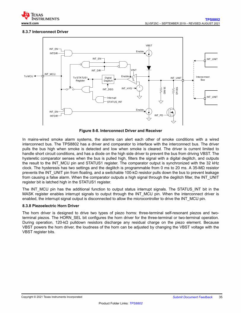
8.3.4 LED Driver
+
–
PDAC_A[7:0]
PLDO
DINA
CSA
1 k
100 F
VBAT LEDLDO
IR LED Blue LED
Blue/IR
LED
LEDPIN_EN
LEDEN
TEMPCOA[1:0]
+
–
PDAC_B[7:0]
PLDO
DINB
CSB
1 k
VBAT LEDLDO
IR LED Blue LED
Blue/IR
LEDTEMPCOB[1:0]
LEDSEL=0
LED LDO
VBST
LEDLDO_EN
LEDLDO[0:2]
LEDLDO
RCSA
100 F
RCSB
PGND
PGND
To MCU
LED
DAC
LED
DAC
GPIO
Logic
To MCU GPIO
GPIO[0:2]
0.1
0.1
Figure 8-4. LED Driver Circuit
8.3.4.1 LED Current Sink
The two LED drivers are current regulated, temperature compensated, and adjustable with an 8-bit DAC. When the LED driver is enabled, the CSA voltage is regulated, and the current through the CSA resistor also flows through the LED and the DINA pin. A current sense resistor connects to the CSA pin. The LED driver is enabled with the LEDEN pin and LEDPIN_EN bit. Both the pin and bit must be high for the LED driver to operate. The LEDSEL bit switches which driver the LEDEN signal connects to. The GPIO pin can be configured to enable either LED driver.
The LED driver is temperature compensated to account for reduced LED intensity with increasing temperature. Four temperature compensation settings are available to support a variety of IR and blue LEDs. Temperature compensation is implemented by varying the CSA regulated voltage with temperature, thus the temperature compensation also depends on the CSA resistor. Each temperature compensation setting has a different DAC output at room temperature. To achieve a specific temperature compensation and current, the PDAC, TEMPCO, and CSA resistor must all be adjusted according to the Section 9.2.2.2 procedure.
The two LED drivers are interchangeable and support both IR and blue LEDs. The only difference between the two LED drivers is a code CSA_BIN available to improve the LED A driver current accuracy for IR LEDs. CSA_BIN in register 0x00 categorizes CSA voltage for each unit as close to the minimum, below average, above average, or close to the maximum (see Section 8.6). Use CSA_BIN to adjust the DAC and compensate for the variation on the LED A driver's current. After adjusting the DAC, the effective variation is reduced by a factor of 4 for the TEMPCOA = 11, PDAC_A = 00 setting. IR LEDs typically require the TEMPCOA = 11 temperature compensation setting. Therefore, use the LED driver A for powering IR LEDs. If better accuracy is required,
www.ti.comTPS8802
SLVSF25C – SEPTEMBER 2019 – REVISED AUGUST 2021
Copyright © 2021 Texas Instruments Incorporated Submit Document Feedback 29
Product Folder Links: TPS8802
calibrate the LED driver current by connecting the CSA or CSB pin to the microcontroller ADC port, measuring the CSA or CSB voltage, and adjusting PDAC_A or PDAC_B until the required current is achieved.
Ensure that the LED current remains below 550 mA, the pulse width remains below 1 ms, and the duty cycle remains below 1%. There is no protection to prevent operation outside these conditions. Ensure the PDAC and TEMPCO registers are programmed before enabling the LED driver.
8.3.4.2 LED Voltage Supply
Enough voltage must be provided to the LED such that the DINA voltage is at least the dropout voltage (VDINA,DROP) above the CSA voltage while the LED driver is enabled. Ensure the DINA voltage does not exceed 11.5 V. Because of the high LED drive currents, a large capacitor connected to the LED anode is required to provide pulsed power to the LED. Any of the internal regulators ( PLDO, LEDLDO) or external supply (VBAT, VDC) meeting the voltage requirements can be used to charge the LED capacitor. Depending on the LED forward voltage, the LED anode can be connected to the battery or to the LEDLDO. Do not connect the LED anode directly to VBST in low-power applications, because the boost converter output voltage can exceed the DINA absolute maximum.
The LED LDO clamps the VBST voltage and blocks reverse current with an integrated diode. It is current limited to prevent inrush current caused by charging the large capacitor. The regulation voltage is adjustable in the LEDLDO register. The LED LDO may be operated with VBST below the regulation voltage. In this case, the LEDLDO voltage stabilizes to VBST minus a diode voltage drop.
The LED driver current and rise time can vary by a few millivolts and microseconds across the LED anode supply and VCC voltages. It is recommended to use a consistent LED anode voltage whenever the LED driver is enabled. If the LEDLDO is used to supply the LED anode, ensure the boost converter is enabled to the same voltage whenever the LEDLDO is enabled.
Connect a capacitor with a value between 1 µF and 100 µF to the LEDLDO.
TPS8802SLVSF25C – SEPTEMBER 2019 – REVISED AUGUST 2021 www.ti.com
30 Submit Document Feedback Copyright © 2021 Texas Instruments Incorporated
Product Folder Links: TPS8802
8.3.5 Carbon Monoxide Sensor AFE
+
±
COSWRI=1COSWRG=1
VINT
COO
CON
COP
To AMUX
COSWRO=1
10 k ±
100 k CO
Sensor
Working
Counter
0.22 F
100 k
PREF
RI=1 k
RO=100 k
COSWREF=1
VINT
COTEST_DIR
COTEST_EN
+
±
COREF[1:0]
To Photo Amp Reference
COAMP_EN
200 k
VINT
To MCU GPIO
For CO Connectivity Test
Use in place of pull-up resistor and
pull-down FET if PREF_SEL=0
100 k
To Photo
Amp
CO Connectivity Test
COGAIN[1:0]
+
±
300 mV
REF0P3REF0P3_EN
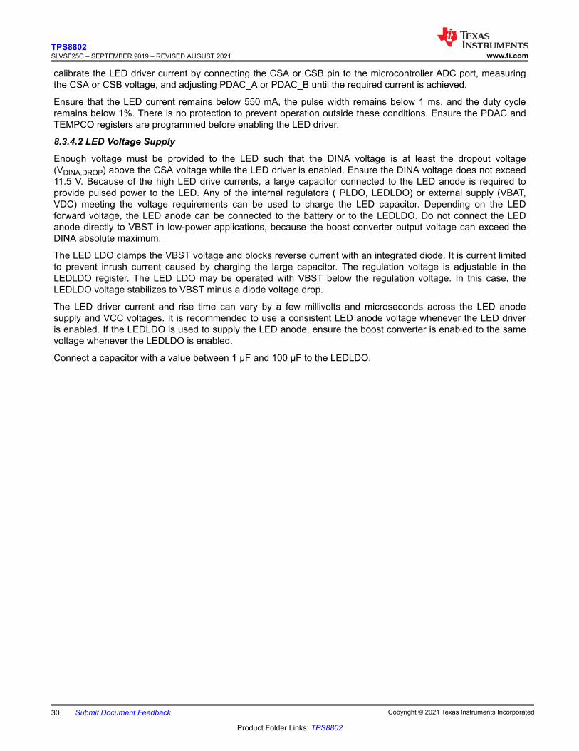
Figure 8-5. Carbon Monoxide Detection Circuit Referenced to GND
www.ti.comTPS8802
SLVSF25C – SEPTEMBER 2019 – REVISED AUGUST 2021
Copyright © 2021 Texas Instruments Incorporated Submit Document Feedback 31
Product Folder Links: TPS8802
+
±
COSWRI=1COSWRG=1
VINT
COO
CON
COP
To AMUX
COSWRO=1
10 k ±
100 k CO
Sensor
Working
Counter
0.22 F
PREF
RI=1 k
RO=100 k
COSWREF=0
VINT
COTEST_DIR
COTEST_EN
+
±
COREF[1:0]
To Photo Amp Reference
COAMP_EN
200 k
VINT
To MCU GPIO
For CO Connectivity Test
Use in place of pull-up resistor and
pull-down FET if PREF_SEL=0
100 k
To Photo
Amp
CO Connectivity Test
COGAIN[1:0]
+
±
300 mV
REF0P3REF0P3_EN100 k
1 nF
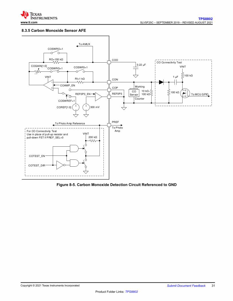
Figure 8-6. Carbon Monoxide Detection Circuit Referenced to 300mV
The TPS8802 CO AFE connects to an electrochemical CO sensor. The amplifier converts the microamps of sensor current into a voltage readable by an ADC. This is achieved with a low-offset, low-power op-amp with configurable input, gain, and output resistors.
8.3.5.1 CO Transimpedance Amplifier
The CO transimpedance amplifier is a low-offset, low-power op-amp with integrated input, gain, and output resistors. Each of these resistors can be disconnected using the COSW register bits if using external resistors. The input resistor limits amplifier current during a CO sensor connectivity test. The gain resistor amplifies the CO sensor signal. Adjust the gain resistor by changing the COGAIN register bits. Use the output resistor with an external capacitor to filter the CO amplifier output signal.
The CO amplifier has two integrated references. A programmable 1.25-mV to 5-mV reference COREF is internally connected to the op-amp positive terminal. A 300-mV reference is connected to the REF0P3 pin. When the millivolt reference is used, the CO sensor must be connected to GND. The millivolt reference is amplified to offset the amplifier output above GND. When the 300 mV reference is used, the reference offsets the CO amplifier output by 300 mV. In general, either reference can be used. The 300-mV reference offers better DC accuracy at the cost of extra power consumption. The 300 mV reference is generated with a reference and op-amp buffer for high precision. The REF0P3 pin must connect to a 1 nF capacitor for stability if it is enabled. The buffer is designed to source and sink small currents as required by the CO amplifier. The 300 mV reference and the 1.25 mV to 5mV reference cannot be enabled simultaneously.
TPS8802SLVSF25C – SEPTEMBER 2019 – REVISED AUGUST 2021 www.ti.com
32 Submit Document Feedback Copyright © 2021 Texas Instruments Incorporated
Product Folder Links: TPS8802
A resistor connected in parallel with the CO sensor prevents charge from accumulating across its terminals. The output of the CO amplifier is connected to the COO pin for continuous monitoring and the AMUX for periodic sampling.
8.3.5.2 CO Connectivity Test
The built-in CO connectivity test function connects to the PREF pin and is available when the photo amplifier is not referenced to PREF. The COTEST_EN and COTEST_DIR register bits program a pull-up and pull-down switch on PREF. A 200 kΩ pull-up resistor charges the 1 µF capacitor when the CO test is not in use. When PREF is pulled low, charge is injected into the amplifier and the output pulse shape can be used to determine if the sensor is connected. An external MOSFET and pull-up resistor achieves the same function as the internal COTEST circuitry.
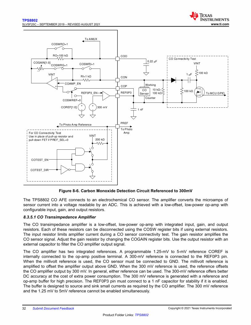
8.3.6 Boost Converter
DCDC
Boost
Hysteretic
Controller
4.7 F
33 H
4.7 F
To Battery
VBST
VLX
VBST_CLIM[3:0]
VBST[3:0]
BST_EN
BST_PG
BST_nACT
PGND
To LED LDO, Battery Test,
Horn Driver, Interconnect
BST_CHARGE
Figure 8-7. DC to DC Hysteretic Boost Circuit
The boost converter operates with a wide range of input and output voltages to support multiple battery configurations and driver voltages. The boost converter output VBST is internally connected to the LED LDO, interconnect driver, horn driver, and battery test load, and may be externally connected to VCC. The boost converter has a power-good register bit BST_PG to notify the MCU when the boost converter is above 95% of the target voltage. The BST_PG signal is deglitched for 200 μs to prevent load transients from causing a false indication. If the BST_PG signal is low after 10 ms of enabling the boost or changing the VBST setting, the BST_ERR signal latches high. The BST_PG signal reads low if the boost converter is disabled.
The boost converter is enabled if any of the following conditions are met:
• BST_EN = 1 or BST_CHARGE=1, except if SLP_BST = 1 and SLP_EN = 1• VCCLOW_BST = 1 and the deglitched VCCLOW comparator trips• Device is in MCULDO_ERR state
The SLP_BST signal disables the boost while the device is in sleep mode if the boost is enabled with BST_EN. The BST_CHARGE register bit enables the boost converter until the BST_PG signal is high, at which point BST_CHARGE resets to 0 and the boost converter is disabled. VCCLOW_BST enables the boost if the deglitched VCCLOW comparator trips. MCULDO_ERR state also enables the boost converter.
A specific I2C command sequence must be used when enabling the boost converter and disabling the photo amplifier. Do not enable the boost converter (changing BST_EN from 0 to 1) and disable the photo input amplifier (changing PAMP_EN from 1 to 0) in the same I2C command. Use either of the following I2C command sequences to enable the boost converter and disable the photo input amplifier:
• Write BST_EN=1 and PAMP_EN=1, then write BST_EN=1 and PAMP_EN=0• Write BST_EN=0 and PAMP_EN=0, then write BST_EN=1 and PAMP_EN=0
www.ti.comTPS8802
SLVSF25C – SEPTEMBER 2019 – REVISED AUGUST 2021
Copyright © 2021 Texas Instruments Incorporated Submit Document Feedback 33
Product Folder Links: TPS8802
8.3.6.1 Boost Hysteretic Control
The hysteretic control guarantees stability across input and output voltages and has a fast transient response. When the VBST voltage is below its target (as programmed in the VBOOST register), a charging cycle initiates by enabling the VLX switch until the current through the inductor exceeds the programmable inductor peak current setting. After the peak current is reached, the VLX switch is disabled and the inductor charges the VBST output capacitor. The charging cycle completes when the inductor current reaches zero, and a new cycle initiates when VBST drops again. Because of the hysteretic control scheme, the average output voltage varies depending on the input voltage, inductor peak current, inductance, output capacitor, output voltage, and output load.
When the VBST voltage is above the boost regulation voltage, the boost does not switch. In a battery backup system, the battery draws no power if the DC supply is providing a VBST voltage above the boost regulation voltage. The boost starts switching if the DC supply drops, drawing power from the battery to regulate VBST. A timer, BST_nACT, monitors the time that the boost is not switching to notify the MCU if the boost is inactive. This timer is programmable from 100 µs to 100 ms. This timer can be used to determine if the battery voltage is higher than the regulation voltage or if an DC supply is connected.
The default inductor peak current is 500 mA. This sets the boost converter to provide maximum output current. After the TPS8802 is powered, the peak current can be adjusted using the I2C interface to change the boost switching frequency or to limit the battery current. The switching frequency is inversely proportional to the square of the current limit. For example, changing the current limit from 500 mA to 50 mA causes the frequency to increase by a factor of 100. The peak current determines how much current the boost converter can output. Equation 1 calculates the maximum boost output current.
IOUT :max ; =D × VBAT × IPEAK
2 × VBST
(1)
Typical boost efficiency is shown in Figure 9-5. If the boost output current draw exceeds the maximum, the boost voltage drops until the converter can supply the output current draw.
8.3.6.2 Boost Soft Start
When the boost converter is enabled and the VBST voltage is below 3 V, the peak inductor current is automatically lowered to reduce inrush current. As a result, the boost converter cannot deliver full output current while the VBST voltage is low. For the 2.7-V boost setting, the inductor current is released to the register value when BST_PG = 1. Maintain the VBST load current below 5 mA during the soft-start period.
TPS8802SLVSF25C – SEPTEMBER 2019 – REVISED AUGUST 2021 www.ti.com
34 Submit Document Feedback Copyright © 2021 Texas Instruments Incorporated
Product Folder Links: TPS8802
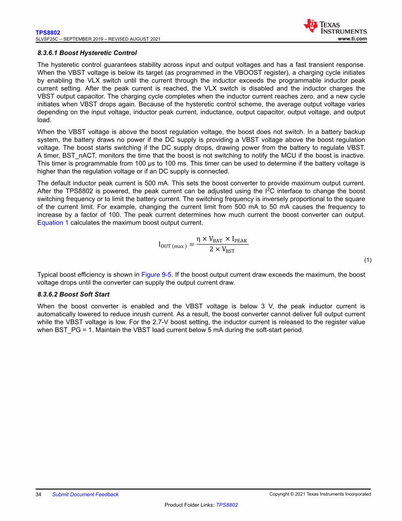
8.3.7 Interconnect Driver
VBST
+
±
+
±
INT_HYS
INT_UNITTo MCU Interconnect
Bus
INTDIR
VINT
INT_EN
INTDIR
INT_EN
INT_PD
35 M
Enable
Enable
Digital
Deglitch
INT_MCU
INT_DEG
INT_UNIT
INT_UNIT
Enable
Interrupt
STATUS_INT
INT_EN
INT_DIR
To STATUS1
Register
Figure 8-8. Interconnect Driver and Receiver
In mains-wired smoke alarm systems, the alarms can alert each other of smoke conditions with a wired interconnect bus. The TPS8802 has a driver and comparator to interface with the interconnect bus. The driver pulls the bus high when smoke is detected and low when smoke is cleared. The driver is current limited to handle short circuit conditions, and has a diode on the high side driver to prevent the bus from driving VBST. The hysteretic comparator senses when the bus is pulled high, filters the signal with a digital deglitch, and outputs the result to the INT_MCU pin and STATUS1 register. The comparator output is synchronized with the 32 kHz clock. The hysteresis has two settings and the deglitch is programmable from 0 ms to 20 ms. A 35-MΩ resistor prevents the INT_UNIT pin from floating, and a switchable 100-kΩ resistor pulls down the bus to prevent leakage from causing a false alarm. When the comparator outputs a high signal through the deglitch filter, the INT_UNIT register bit is latched high in the STATUS1 register.
The INT_MCU pin has the additional function to output status interrupt signals. The STATUS_INT bit in the MASK register enables interrupt signals to output through the INT_MCU pin. When the interconnect driver is enabled, the interrupt signal output is disconnected to allow the microcontroller to drive the INT_MCU pin.
8.3.8 Piezoelectric Horn Driver
The horn driver is designed to drive two types of piezo horns: three-terminal self-resonant piezos and two-terminal piezos. The HORN_SEL bit configures the horn driver for the three-terminal or two-terminal operation. During operation, 120-kΩ pulldown resistors discharge any residual charge on the piezo element. Because VBST powers the horn driver, the loudness of the horn can be adjusted by changing the VBST voltage with the VBST register bits.
www.ti.comTPS8802
SLVSF25C – SEPTEMBER 2019 – REVISED AUGUST 2021
Copyright © 2021 Texas Instruments Incorporated Submit Document Feedback 35
Product Folder Links: TPS8802
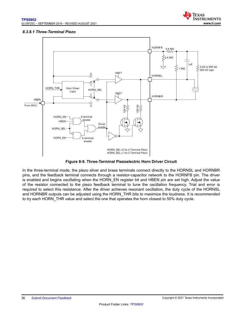
8.3.8.1 Three-Terminal Piezo
HBEN
VBST
HORN_SEL=0 for 2 Terminal Piezo
HORN_SEL=1 for 3 Terminal Piezo
From MCU
12
0 k
HORN_EN
HBEN
HORN_SEL
HORN_EN
3-terminal
enable
2-terminal
enable
HORN_SEL
12
0 k
Driver
enable
Horn Driver
LogicVBST
0
1
1
0
HORN_THR
5.6 M
HORNSL
HORNBR
HORNFB
1nF
2.4 M
0 k to 500 k
220 k (typ)1 M
Figure 8-9. Three-Terminal Piezoelectric Horn Driver Circuit
In the three-terminal mode, the piezo silver and brass terminals connect directly to the HORNSL and HORNBR pins, and the feedback terminal connects through a resistor-capacitor network to the HORNFB pin. The driver is enabled and begins oscillating when the HORN_EN register bit and HBEN pin are set high. Adjust the value of the resistor connected to the piezo feedback terminal to tune the oscillation frequency. Trial and error is required to select this resistance. After the driver achieves resonant oscillation, the duty cycle of the HORNSL and HORNBR outputs can be adjusted using the HORN_THR bits to maximize the loudness. It is recommended to try each HORN_THR value and select the one that operates the horn closest to 50% duty cycle.
TPS8802SLVSF25C – SEPTEMBER 2019 – REVISED AUGUST 2021 www.ti.com
36 Submit Document Feedback Copyright © 2021 Texas Instruments Incorporated
Product Folder Links: TPS8802
8.3.8.2 Two-Terminal Piezo
HBEN
VBST
HORN_SEL=0 for 2 Terminal Piezo
HORN_SEL=1 for 3 Terminal Piezo
HORNSL
HORNBR
HORNFB
From MCU
120
k
HORN_EN
HBEN
HORN_SEL
HORN_EN
3-terminal
enable
2-terminal
enable
HORN_SEL
120
k
Driver
enable
Horn Driver
LogicVBST
1 mH
From MCU
0
1
1
0
HORN_THR
Figure 8-10. Two-Terminal Piezoelectric Horn Driver Circuit
In the two-terminal mode, the piezo connects to the HORNSL and HORNBR terminals through an inductor. The HORNFB pin directly controls the HORNSL pin, and the HBEN pin directly controls the HORNBR pin. The two drivers are matched to minimize skew between the two outputs. The MCU sends a digital signal to control the driving voltage across the piezo. The signal can be a square wave of the oscillation frequency, a pulse width modulation (PWM) sine wave of the oscillation frequency, or a PWM arbitrary shape for voice applications. The inductor improves the rise time and fall time of the output and reduces power dissipation.
8.3.9 Battery Test
The battery test load is used to check the integrity of the battery connected to the TPS8802 device. When enabled, a load is connected to VBST. The load is programmable from 10 mA to 20 mA with the I_BATTEST register bits. This load emulates the horn driver current draw during an alarm condition. The boost input voltage, output voltage, and efficiency affect the current drawn from the battery because the battery test load is connected to VBST. Therefore, the battery current is programmable with the VBST register as well. Ensure VBST is greater than 4.5 V when enabling the battery test load. The load is enabled with the BATTEST_EN register bit or with the GPIO register bit and pin.
www.ti.comTPS8802
SLVSF25C – SEPTEMBER 2019 – REVISED AUGUST 2021
Copyright © 2021 Texas Instruments Incorporated Submit Document Feedback 37
Product Folder Links: TPS8802
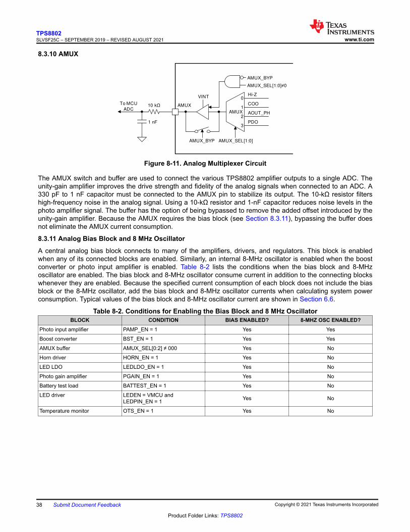
8.3.10 AMUX
Hi-Z
COO
AOUT_PH
PDO
0
1
2
3
AMUX_BYP
AMUX_SEL[1:0]0
VINT
AMUX_BYP
AMUX
10 k
1 nF
To MCU
ADCAMUX
AMUX_SEL[1:0]
Figure 8-11. Analog Multiplexer Circuit
The AMUX switch and buffer are used to connect the various TPS8802 amplifier outputs to a single ADC. The unity-gain amplifier improves the drive strength and fidelity of the analog signals when connected to an ADC. A 330 pF to 1 nF capacitor must be connected to the AMUX pin to stabilize its output. The 10-kΩ resistor filters high-frequency noise in the analog signal. Using a 10-kΩ resistor and 1-nF capacitor reduces noise levels in the photo amplifier signal. The buffer has the option of being bypassed to remove the added offset introduced by the unity-gain amplifier. Because the AMUX requires the bias block (see Section 8.3.11), bypassing the buffer does not eliminate the AMUX current consumption.
8.3.11 Analog Bias Block and 8 MHz Oscillator
A central analog bias block connects to many of the amplifiers, drivers, and regulators. This block is enabled when any of its connected blocks are enabled. Similarly, an internal 8-MHz oscillator is enabled when the boost converter or photo input amplifier is enabled. Table 8-2 lists the conditions when the bias block and 8-MHz oscillator are enabled. The bias block and 8-MHz oscillator consume current in addition to the connecting blocks whenever they are enabled. Because the specified current consumption of each block does not include the bias block or the 8-MHz oscillator, add the bias block and 8-MHz oscillator currents when calculating system power consumption. Typical values of the bias block and 8-MHz oscillator current are shown in Section 6.6.
Table 8-2. Conditions for Enabling the Bias Block and 8 MHz OscillatorBLOCK CONDITION BIAS ENABLED? 8-MHZ OSC ENABLED?
Photo input amplifier PAMP_EN = 1 Yes Yes
Boost converter BST_EN = 1 Yes Yes
AMUX buffer AMUX_SEL[0:2] ≠ 000 Yes No
Horn driver HORN_EN = 1 Yes No
LED LDO LEDLDO_EN = 1 Yes No
Photo gain amplifier PGAIN_EN = 1 Yes No
Battery test load BATTEST_EN = 1 Yes No
LED driver LEDEN = VMCU and LEDPIN_EN = 1 Yes No
Temperature monitor OTS_EN = 1 Yes No
TPS8802SLVSF25C – SEPTEMBER 2019 – REVISED AUGUST 2021 www.ti.com
38 Submit Document Feedback Copyright © 2021 Texas Instruments Incorporated
Product Folder Links: TPS8802
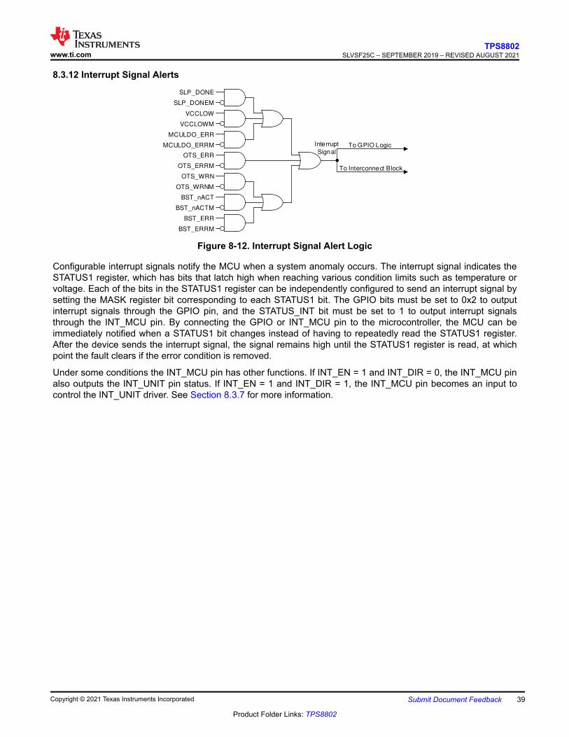
8.3.12 Interrupt Signal AlertsSLP_DONE
VCCLOW
SLP_DONEM
VCCLOWM
OTS_ERR
OTS_ERRM
MCULDO_ERR
MCULDO_ERRM
OTS_WRN
OTS_WRNM
BST_nACT
BST_nACTM
BST_ERR
BST_ERRM
To GPIO Logic
To Interconnect Block
Interrupt
Signal
Figure 8-12. Interrupt Signal Alert Logic
Configurable interrupt signals notify the MCU when a system anomaly occurs. The interrupt signal indicates the STATUS1 register, which has bits that latch high when reaching various condition limits such as temperature or voltage. Each of the bits in the STATUS1 register can be independently configured to send an interrupt signal by setting the MASK register bit corresponding to each STATUS1 bit. The GPIO bits must be set to 0x2 to output interrupt signals through the GPIO pin, and the STATUS_INT bit must be set to 1 to output interrupt signals through the INT_MCU pin. By connecting the GPIO or INT_MCU pin to the microcontroller, the MCU can be immediately notified when a STATUS1 bit changes instead of having to repeatedly read the STATUS1 register. After the device sends the interrupt signal, the signal remains high until the STATUS1 register is read, at which point the fault clears if the error condition is removed.
Under some conditions the INT_MCU pin has other functions. If INT_EN = 1 and INT_DIR = 0, the INT_MCU pin also outputs the INT_UNIT pin status. If INT_EN = 1 and INT_DIR = 1, the INT_MCU pin becomes an input to control the INT_UNIT driver. See Section 8.3.7 for more information.
www.ti.comTPS8802
SLVSF25C – SEPTEMBER 2019 – REVISED AUGUST 2021
Copyright © 2021 Texas Instruments Incorporated Submit Document Feedback 39
Product Folder Links: TPS8802
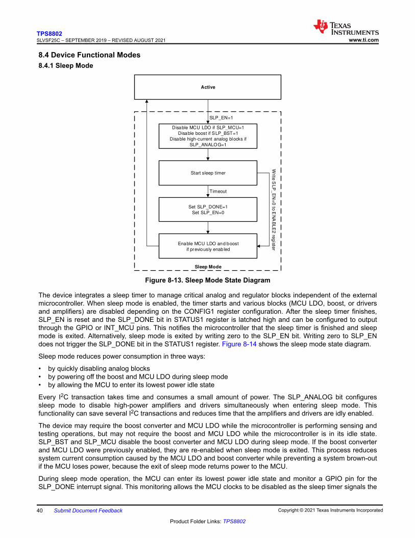
8.4 Device Functional Modes8.4.1 Sleep Mode
Active
Disable MCU LDO if SLP_MCU=1
Disable boost if SLP_BST=1
Disable high-current analog blocks if
SLP_ANALOG=1
SLP_EN=1
Start sleep timer
Set SLP_DONE=1
Set SLP_EN=0
Write
SLP
_E
N=
0 to
EN
AB
LE
2 re
giste
r
Enable MCU LDO and boost
if previously enabled
Timeout
Sleep Mode
Figure 8-13. Sleep Mode State Diagram
The device integrates a sleep timer to manage critical analog and regulator blocks independent of the external microcontroller. When sleep mode is enabled, the timer starts and various blocks (MCU LDO, boost, or drivers and amplifiers) are disabled depending on the CONFIG1 register configuration. After the sleep timer finishes, SLP_EN is reset and the SLP_DONE bit in STATUS1 register is latched high and can be configured to output through the GPIO or INT_MCU pins. This notifies the microcontroller that the sleep timer is finished and sleep mode is exited. Alternatively, sleep mode is exited by writing zero to the SLP_EN bit. Writing zero to SLP_EN does not trigger the SLP_DONE bit in the STATUS1 register. Figure 8-14 shows the sleep mode state diagram.
Sleep mode reduces power consumption in three ways:
• by quickly disabling analog blocks• by powering off the boost and MCU LDO during sleep mode• by allowing the MCU to enter its lowest power idle state
Every I2C transaction takes time and consumes a small amount of power. The SLP_ANALOG bit configures sleep mode to disable high-power amplifiers and drivers simultaneously when entering sleep mode. This functionality can save several I2C transactions and reduces time that the amplifiers and drivers are idly enabled.
The device may require the boost converter and MCU LDO while the microcontroller is performing sensing and testing operations, but may not require the boost and MCU LDO while the microcontroller is in its idle state. SLP_BST and SLP_MCU disable the boost converter and MCU LDO during sleep mode. If the boost converter and MCU LDO were previously enabled, they are re-enabled when sleep mode is exited. This process reduces system current consumption caused by the MCU LDO and boost converter while preventing a system brown-out if the MCU loses power, because the exit of sleep mode returns power to the MCU.
During sleep mode operation, the MCU can enter its lowest power idle state and monitor a GPIO pin for the SLP_DONE interrupt signal. This monitoring allows the MCU clocks to be disabled as the sleep timer signals the
TPS8802SLVSF25C – SEPTEMBER 2019 – REVISED AUGUST 2021 www.ti.com
40 Submit Document Feedback Copyright © 2021 Texas Instruments Incorporated
Product Folder Links: TPS8802
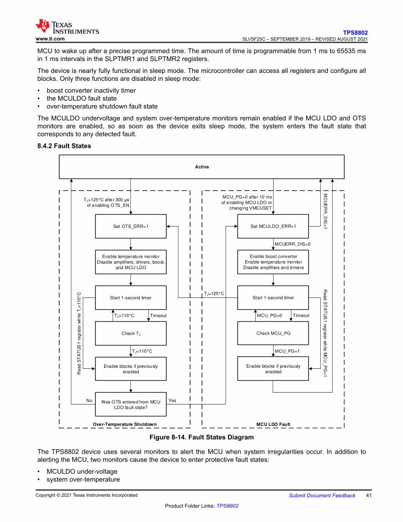
MCU to wake up after a precise programmed time. The amount of time is programmable from 1 ms to 65535 ms in 1 ms intervals in the SLPTMR1 and SLPTMR2 registers.
The device is nearly fully functional in sleep mode. The microcontroller can access all registers and configure all blocks. Only three functions are disabled in sleep mode:
• boost converter inactivity timer• the MCULDO fault state• over-temperature shutdown fault state
The MCULDO undervoltage and system over-temperature monitors remain enabled if the MCU LDO and OTS monitors are enabled, so as soon as the device exits sleep mode, the system enters the fault state that corresponds to any detected fault.
8.4.2 Fault States
Active
Set OTS_ERR=1
TJ>125°C after 300 µs
of enabling OTS_EN
Enable temperature monitor
Disable amplifiers, drivers, boost,
and MCU LDO
Start 1-second timer
Check TJ
TimeoutTJ>110°C
Enable blocks if previously
enabledRead S
TA
TU
S1 r
egis
ter
wh
ile T
J<
110
°C
Was OTS entered from MCU
LDO fault state?
Set MCULDO_ERR=1
Enable boost converter
Enable temperature monitor
Disable amplifiers and drivers
Start 1-second timer
Check MCU_PG
MCU_PG=0 Timeout
MCU_PG=1
MCU_PG=0 after 10 ms
of enabling MCU LDO or
changing VMCUSET
No Yes
Enable blocks if previously
enabled
TJ<110°C
TJ>125°C
Read S
TA
TU
S1 re
giste
r wh
ile M
CU
_P
G=
1
Over-Temperature Shutdown MCU LDO Fault
MCUERR_DIS=0
MC
UE
RR
_D
IS=
1
Figure 8-14. Fault States Diagram
The TPS8802 device uses several monitors to alert the MCU when system irregularities occur. In addition to alerting the MCU, two monitors cause the device to enter protective fault states:
• MCULDO under-voltage• system over-temperature
www.ti.comTPS8802
SLVSF25C – SEPTEMBER 2019 – REVISED AUGUST 2021
Copyright © 2021 Texas Instruments Incorporated Submit Document Feedback 41
Product Folder Links: TPS8802
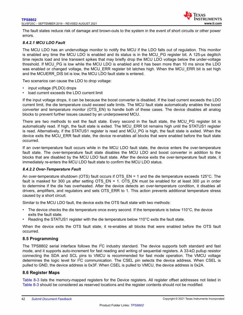
The fault states reduce risk of damage and brown-outs to the system in the event of short circuits or other power errors.
8.4.2.1 MCU LDO Fault
The MCU LDO has an undervoltage monitor to notify the MCU if the LDO falls out of regulation. This monitor is enabled any time the MCU LDO is enabled and its status is in the MCU_PG register bit. A 125-μs deglitch time rejects load and line transient spikes that may briefly drop the MCU LDO voltage below the under-voltage threshold. If MCU_PG is low while the MCU LDO is enabled and it has been more than 10 ms since the LDO was enabled or changed voltage, the MCU_ERR register bit latches high. When the MCU_ERR bit is set high and the MCUERR_DIS bit is low, the MCU LDO fault state is entered.
Two scenarios can cause the LDO to drop voltage:
• input voltage (PLDO) drops• load current exceeds the LDO current limit
If the input voltage drops, it can be because the boost converter is disabled. If the load current exceeds the LDO current limit, the die temperature could exceed safe limits. The MCU fault state automatically enables the boost converter and temperature monitor (OTS_EN) to handle both of these cases. The device disables all analog blocks to prevent further issues caused by an underpowered MCU.
There are two methods to exit the fault state. Every second in the fault state, the MCU_PG register bit is automatically read. If high, the fault state is exited. The MCU_ERR bit remains high until the STATUS1 register is read. Alternatively, if the STATUS1 register is read and MCU_PG is high, the fault state is exited. When the device exits the MCU_ERR fault state, the device re-enables all blocks that were enabled before the fault state occurred.
If an over-temperature fault occurs while in the MCU LDO fault state, the device enters the over-temperature fault state. The over-temperature fault state disables the MCU LDO and boost converter in addition to the blocks that are disabled by the MCU LDO fault state. After the device exits the over-temperature fault state, it immediately re-enters the MCU LDO fault state to confirm the MCU LDO status.
8.4.2.2 Over-Temperature Fault
An over-temperature shutdown (OTS) fault occurs if OTS_EN = 1 and the die temperature exceeds 125°C. The fault is masked for 300 μs after setting OTS_EN = 1. OTS_EN must be enabled for at least 300 μs in order to determine if the die has overheated. After the device detects an over-temperature condition, it disables all drivers, amplifiers, and regulators and sets OTS_ERR to 1. This action prevents additional temperature stress caused by a short circuit.
Similar to the MCU LDO fault, the device exits the OTS fault state with two methods:
• The device checks the die temperature once every second. If the temperature is below 110°C, the device exits the fault state.
• Reading the STATUS1 register with the die temperature below 110°C exits the fault state.
When the device exits the OTS fault state, it re-enables all blocks that were enabled before the OTS fault occurred.
8.5 ProgrammingThe TPS8802 serial interface follows the I2C industry standard. The device supports both standard and fast mode, and it supports auto-increment for fast reading and writing of sequential registers. A 33-kΩ pullup resistor connecting the SDA and SCL pins to VMCU is recommended for fast mode operation. The VMCU voltage determines the logic level for I2C communication. The CSEL pin selects the device address. When CSEL is pulled to GND, the device address is 0x3F. When CSEL is pulled to VMCU, the device address is 0x2A.
8.6 Register MapsTable 8-3 lists the memory-mapped registers for the Device registers. All register offset addresses not listed in Table 8-3 should be considered as reserved locations and the register contents should not be modified.
TPS8802SLVSF25C – SEPTEMBER 2019 – REVISED AUGUST 2021 www.ti.com
42 Submit Document Feedback Copyright © 2021 Texas Instruments Incorporated
Product Folder Links: TPS8802
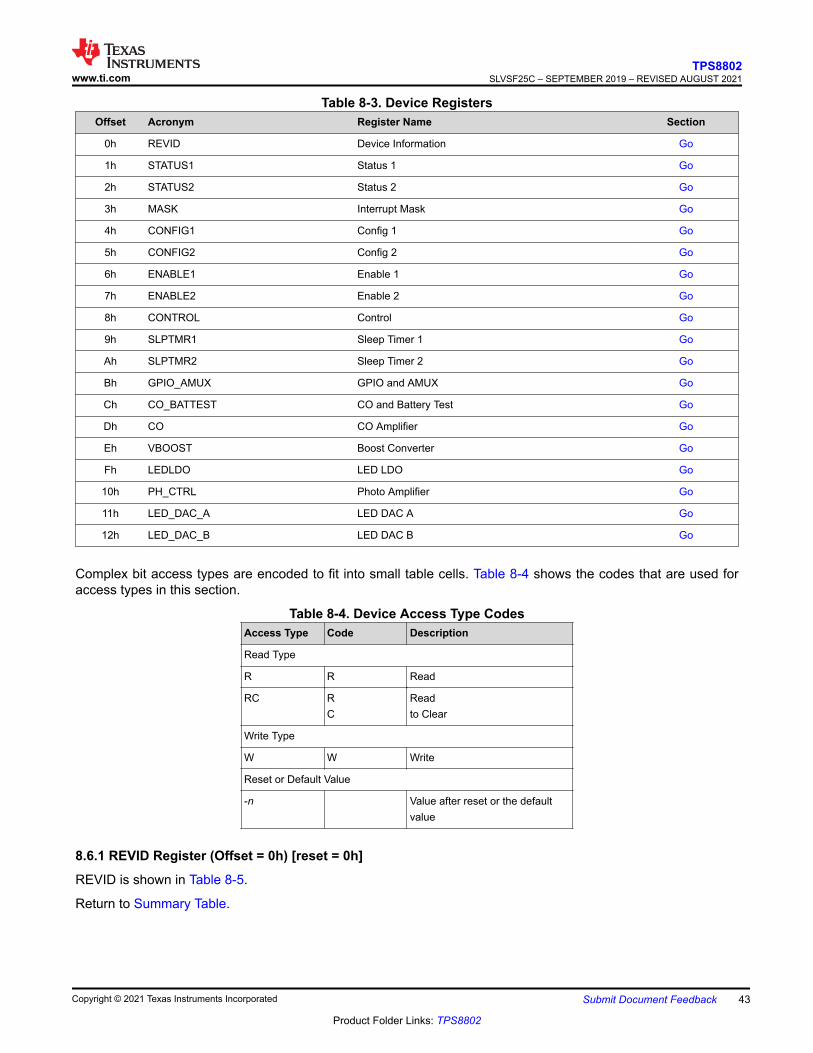
Table 8-3. Device RegistersOffset Acronym Register Name Section
0h REVID Device Information Go
1h STATUS1 Status 1 Go
2h STATUS2 Status 2 Go
3h MASK Interrupt Mask Go
4h CONFIG1 Config 1 Go
5h CONFIG2 Config 2 Go
6h ENABLE1 Enable 1 Go
7h ENABLE2 Enable 2 Go
8h CONTROL Control Go
9h SLPTMR1 Sleep Timer 1 Go
Ah SLPTMR2 Sleep Timer 2 Go
Bh GPIO_AMUX GPIO and AMUX Go
Ch CO_BATTEST CO and Battery Test Go
Dh CO CO Amplifier Go
Eh VBOOST Boost Converter Go
Fh LEDLDO LED LDO Go
10h PH_CTRL Photo Amplifier Go
11h LED_DAC_A LED DAC A Go
12h LED_DAC_B LED DAC B Go
Complex bit access types are encoded to fit into small table cells. Table 8-4 shows the codes that are used for access types in this section.
Table 8-4. Device Access Type CodesAccess Type Code Description
Read Type
R R Read
RC RC
Readto Clear
Write Type
W W Write
Reset or Default Value
-n Value after reset or the default value
8.6.1 REVID Register (Offset = 0h) [reset = 0h]
REVID is shown in Table 8-5.
Return to Summary Table.
www.ti.comTPS8802
SLVSF25C – SEPTEMBER 2019 – REVISED AUGUST 2021
Copyright © 2021 Texas Instruments Incorporated Submit Document Feedback 43
Product Folder Links: TPS8802
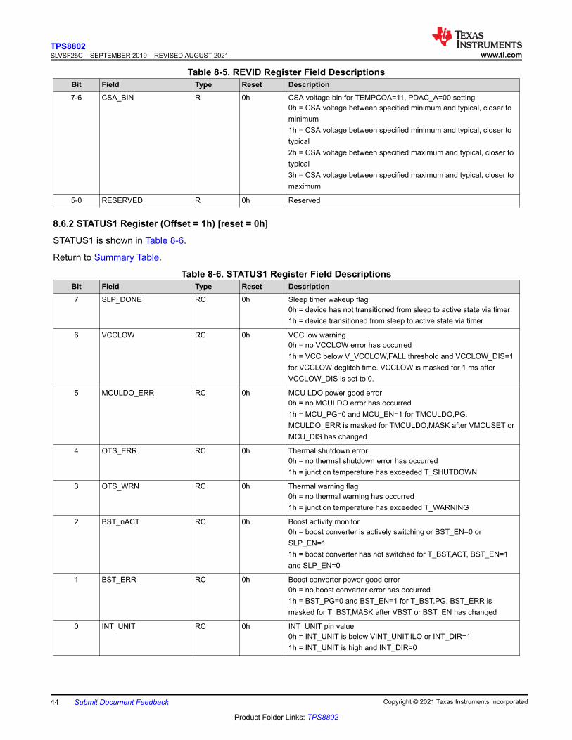
Table 8-5. REVID Register Field DescriptionsBit Field Type Reset Description7-6 CSA_BIN R 0h CSA voltage bin for TEMPCOA=11, PDAC_A=00 setting
0h = CSA voltage between specified minimum and typical, closer to minimum1h = CSA voltage between specified minimum and typical, closer to typical2h = CSA voltage between specified maximum and typical, closer to typical3h = CSA voltage between specified maximum and typical, closer to maximum
5-0 RESERVED R 0h Reserved
8.6.2 STATUS1 Register (Offset = 1h) [reset = 0h]
STATUS1 is shown in Table 8-6.
Return to Summary Table.
Table 8-6. STATUS1 Register Field DescriptionsBit Field Type Reset Description7 SLP_DONE RC 0h Sleep timer wakeup flag
0h = device has not transitioned from sleep to active state via timer1h = device transitioned from sleep to active state via timer
6 VCCLOW RC 0h VCC low warning0h = no VCCLOW error has occurred1h = VCC below V_VCCLOW,FALL threshold and VCCLOW_DIS=1 for VCCLOW deglitch time. VCCLOW is masked for 1 ms after VCCLOW_DIS is set to 0.
5 MCULDO_ERR RC 0h MCU LDO power good error0h = no MCULDO error has occurred1h = MCU_PG=0 and MCU_EN=1 for TMCULDO,PG. MCULDO_ERR is masked for TMCULDO,MASK after VMCUSET or MCU_DIS has changed
4 OTS_ERR RC 0h Thermal shutdown error0h = no thermal shutdown error has occurred1h = junction temperature has exceeded T_SHUTDOWN
3 OTS_WRN RC 0h Thermal warning flag0h = no thermal warning has occurred1h = junction temperature has exceeded T_WARNING
2 BST_nACT RC 0h Boost activity monitor0h = boost converter is actively switching or BST_EN=0 or SLP_EN=11h = boost converter has not switched for T_BST,ACT, BST_EN=1 and SLP_EN=0
1 BST_ERR RC 0h Boost converter power good error0h = no boost converter error has occurred1h = BST_PG=0 and BST_EN=1 for T_BST,PG. BST_ERR is masked for T_BST,MASK after VBST or BST_EN has changed
0 INT_UNIT RC 0h INT_UNIT pin value0h = INT_UNIT is below VINT_UNIT,ILO or INT_DIR=11h = INT_UNIT is high and INT_DIR=0
TPS8802SLVSF25C – SEPTEMBER 2019 – REVISED AUGUST 2021 www.ti.com
44 Submit Document Feedback Copyright © 2021 Texas Instruments Incorporated
Product Folder Links: TPS8802
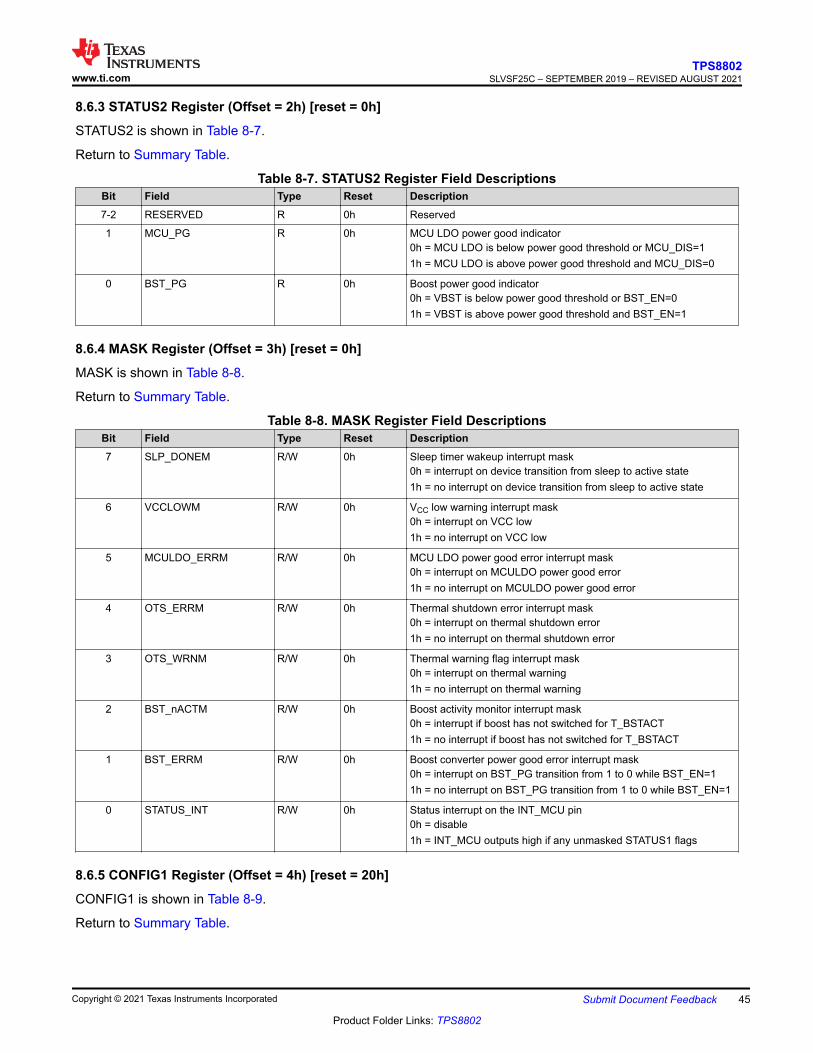
8.6.3 STATUS2 Register (Offset = 2h) [reset = 0h]
STATUS2 is shown in Table 8-7.
Return to Summary Table.
Table 8-7. STATUS2 Register Field DescriptionsBit Field Type Reset Description7-2 RESERVED R 0h Reserved
1 MCU_PG R 0h MCU LDO power good indicator0h = MCU LDO is below power good threshold or MCU_DIS=11h = MCU LDO is above power good threshold and MCU_DIS=0
0 BST_PG R 0h Boost power good indicator0h = VBST is below power good threshold or BST_EN=01h = VBST is above power good threshold and BST_EN=1
8.6.4 MASK Register (Offset = 3h) [reset = 0h]
MASK is shown in Table 8-8.
Return to Summary Table.
Table 8-8. MASK Register Field DescriptionsBit Field Type Reset Description7 SLP_DONEM R/W 0h Sleep timer wakeup interrupt mask
0h = interrupt on device transition from sleep to active state1h = no interrupt on device transition from sleep to active state
6 VCCLOWM R/W 0h VCC low warning interrupt mask0h = interrupt on VCC low1h = no interrupt on VCC low
5 MCULDO_ERRM R/W 0h MCU LDO power good error interrupt mask0h = interrupt on MCULDO power good error1h = no interrupt on MCULDO power good error
4 OTS_ERRM R/W 0h Thermal shutdown error interrupt mask0h = interrupt on thermal shutdown error1h = no interrupt on thermal shutdown error
3 OTS_WRNM R/W 0h Thermal warning flag interrupt mask0h = interrupt on thermal warning1h = no interrupt on thermal warning
2 BST_nACTM R/W 0h Boost activity monitor interrupt mask0h = interrupt if boost has not switched for T_BSTACT1h = no interrupt if boost has not switched for T_BSTACT
1 BST_ERRM R/W 0h Boost converter power good error interrupt mask0h = interrupt on BST_PG transition from 1 to 0 while BST_EN=11h = no interrupt on BST_PG transition from 1 to 0 while BST_EN=1
0 STATUS_INT R/W 0h Status interrupt on the INT_MCU pin0h = disable1h = INT_MCU outputs high if any unmasked STATUS1 flags
8.6.5 CONFIG1 Register (Offset = 4h) [reset = 20h]
CONFIG1 is shown in Table 8-9.
Return to Summary Table.
www.ti.comTPS8802
SLVSF25C – SEPTEMBER 2019 – REVISED AUGUST 2021
Copyright © 2021 Texas Instruments Incorporated Submit Document Feedback 45
Product Folder Links: TPS8802
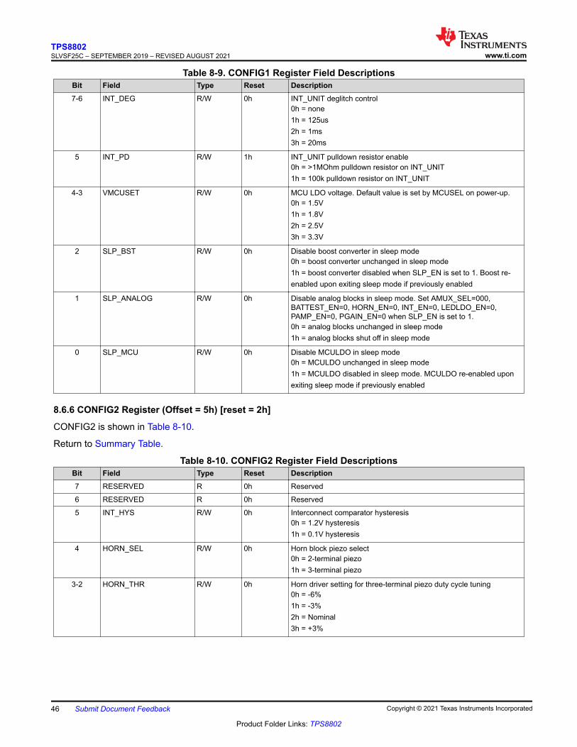
Table 8-9. CONFIG1 Register Field DescriptionsBit Field Type Reset Description7-6 INT_DEG R/W 0h INT_UNIT deglitch control
0h = none1h = 125us2h = 1ms3h = 20ms
5 INT_PD R/W 1h INT_UNIT pulldown resistor enable0h = >1MOhm pulldown resistor on INT_UNIT1h = 100k pulldown resistor on INT_UNIT
4-3 VMCUSET R/W 0h MCU LDO voltage. Default value is set by MCUSEL on power-up.0h = 1.5V1h = 1.8V2h = 2.5V3h = 3.3V
2 SLP_BST R/W 0h Disable boost converter in sleep mode0h = boost converter unchanged in sleep mode1h = boost converter disabled when SLP_EN is set to 1. Boost re-enabled upon exiting sleep mode if previously enabled
1 SLP_ANALOG R/W 0h Disable analog blocks in sleep mode. Set AMUX_SEL=000, BATTEST_EN=0, HORN_EN=0, INT_EN=0, LEDLDO_EN=0, PAMP_EN=0, PGAIN_EN=0 when SLP_EN is set to 1.0h = analog blocks unchanged in sleep mode1h = analog blocks shut off in sleep mode
0 SLP_MCU R/W 0h Disable MCULDO in sleep mode0h = MCULDO unchanged in sleep mode1h = MCULDO disabled in sleep mode. MCULDO re-enabled upon exiting sleep mode if previously enabled
8.6.6 CONFIG2 Register (Offset = 5h) [reset = 2h]
CONFIG2 is shown in Table 8-10.
Return to Summary Table.
Table 8-10. CONFIG2 Register Field DescriptionsBit Field Type Reset Description7 RESERVED R 0h Reserved
6 RESERVED R 0h Reserved
5 INT_HYS R/W 0h Interconnect comparator hysteresis0h = 1.2V hysteresis1h = 0.1V hysteresis
4 HORN_SEL R/W 0h Horn block piezo select0h = 2-terminal piezo1h = 3-terminal piezo
3-2 HORN_THR R/W 0h Horn driver setting for three-terminal piezo duty cycle tuning0h = -6%1h = -3%2h = Nominal3h = +3%
TPS8802SLVSF25C – SEPTEMBER 2019 – REVISED AUGUST 2021 www.ti.com
46 Submit Document Feedback Copyright © 2021 Texas Instruments Incorporated
Product Folder Links: TPS8802
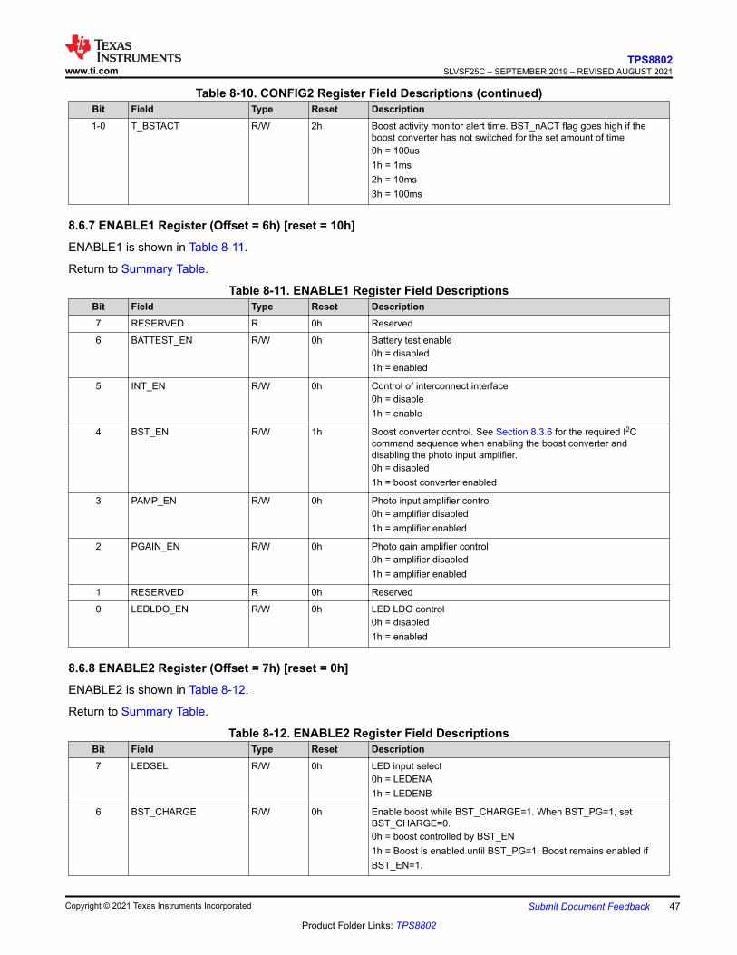
Table 8-10. CONFIG2 Register Field Descriptions (continued)Bit Field Type Reset Description1-0 T_BSTACT R/W 2h Boost activity monitor alert time. BST_nACT flag goes high if the
boost converter has not switched for the set amount of time0h = 100us1h = 1ms2h = 10ms3h = 100ms
8.6.7 ENABLE1 Register (Offset = 6h) [reset = 10h]
ENABLE1 is shown in Table 8-11.
Return to Summary Table.
Table 8-11. ENABLE1 Register Field DescriptionsBit Field Type Reset Description7 RESERVED R 0h Reserved
6 BATTEST_EN R/W 0h Battery test enable0h = disabled1h = enabled
5 INT_EN R/W 0h Control of interconnect interface0h = disable1h = enable
4 BST_EN R/W 1h Boost converter control. See Section 8.3.6 for the required I2C command sequence when enabling the boost converter and disabling the photo input amplifier.0h = disabled1h = boost converter enabled
3 PAMP_EN R/W 0h Photo input amplifier control0h = amplifier disabled1h = amplifier enabled
2 PGAIN_EN R/W 0h Photo gain amplifier control0h = amplifier disabled1h = amplifier enabled
1 RESERVED R 0h Reserved
0 LEDLDO_EN R/W 0h LED LDO control0h = disabled1h = enabled
8.6.8 ENABLE2 Register (Offset = 7h) [reset = 0h]
ENABLE2 is shown in Table 8-12.
Return to Summary Table.
Table 8-12. ENABLE2 Register Field DescriptionsBit Field Type Reset Description7 LEDSEL R/W 0h LED input select
0h = LEDENA1h = LEDENB
6 BST_CHARGE R/W 0h Enable boost while BST_CHARGE=1. When BST_PG=1, set BST_CHARGE=0.0h = boost controlled by BST_EN1h = Boost is enabled until BST_PG=1. Boost remains enabled if BST_EN=1.
www.ti.comTPS8802
SLVSF25C – SEPTEMBER 2019 – REVISED AUGUST 2021
Copyright © 2021 Texas Instruments Incorporated Submit Document Feedback 47
Product Folder Links: TPS8802
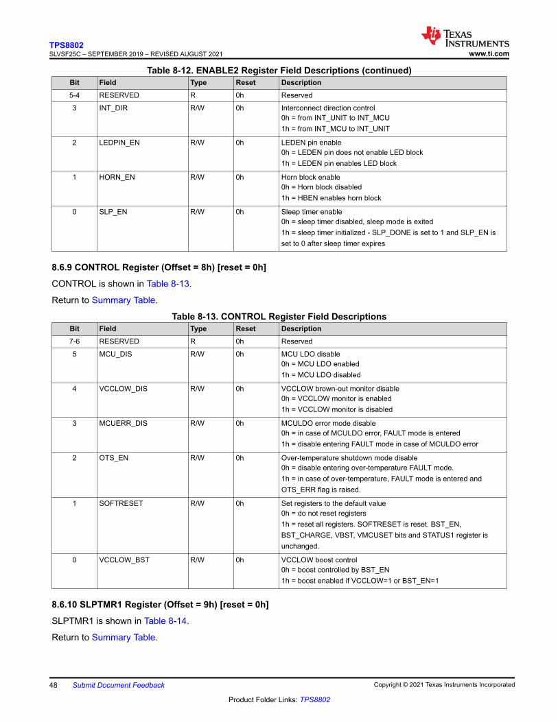
Table 8-12. ENABLE2 Register Field Descriptions (continued)Bit Field Type Reset Description5-4 RESERVED R 0h Reserved
3 INT_DIR R/W 0h Interconnect direction control0h = from INT_UNIT to INT_MCU1h = from INT_MCU to INT_UNIT
2 LEDPIN_EN R/W 0h LEDEN pin enable0h = LEDEN pin does not enable LED block1h = LEDEN pin enables LED block
1 HORN_EN R/W 0h Horn block enable0h = Horn block disabled1h = HBEN enables horn block
0 SLP_EN R/W 0h Sleep timer enable0h = sleep timer disabled, sleep mode is exited1h = sleep timer initialized - SLP_DONE is set to 1 and SLP_EN is set to 0 after sleep timer expires
8.6.9 CONTROL Register (Offset = 8h) [reset = 0h]
CONTROL is shown in Table 8-13.
Return to Summary Table.
Table 8-13. CONTROL Register Field DescriptionsBit Field Type Reset Description7-6 RESERVED R 0h Reserved
5 MCU_DIS R/W 0h MCU LDO disable0h = MCU LDO enabled1h = MCU LDO disabled
4 VCCLOW_DIS R/W 0h VCCLOW brown-out monitor disable0h = VCCLOW monitor is enabled1h = VCCLOW monitor is disabled
3 MCUERR_DIS R/W 0h MCULDO error mode disable0h = in case of MCULDO error, FAULT mode is entered1h = disable entering FAULT mode in case of MCULDO error
2 OTS_EN R/W 0h Over-temperature shutdown mode disable0h = disable entering over-temperature FAULT mode.1h = in case of over-temperature, FAULT mode is entered and OTS_ERR flag is raised.
1 SOFTRESET R/W 0h Set registers to the default value0h = do not reset registers1h = reset all registers. SOFTRESET is reset. BST_EN, BST_CHARGE, VBST, VMCUSET bits and STATUS1 register is unchanged.
0 VCCLOW_BST R/W 0h VCCLOW boost control0h = boost controlled by BST_EN1h = boost enabled if VCCLOW=1 or BST_EN=1
8.6.10 SLPTMR1 Register (Offset = 9h) [reset = 0h]
SLPTMR1 is shown in Table 8-14.
Return to Summary Table.
TPS8802SLVSF25C – SEPTEMBER 2019 – REVISED AUGUST 2021 www.ti.com
48 Submit Document Feedback Copyright © 2021 Texas Instruments Incorporated
Product Folder Links: TPS8802
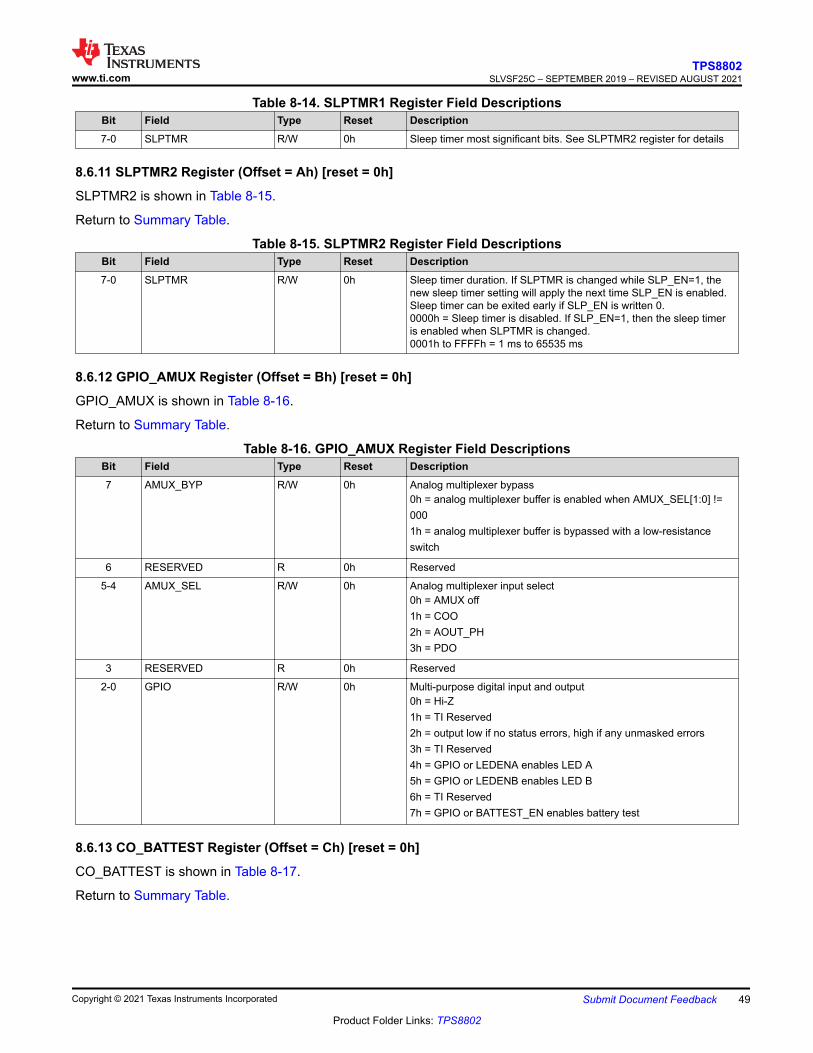
Table 8-14. SLPTMR1 Register Field DescriptionsBit Field Type Reset Description7-0 SLPTMR R/W 0h Sleep timer most significant bits. See SLPTMR2 register for details
8.6.11 SLPTMR2 Register (Offset = Ah) [reset = 0h]
SLPTMR2 is shown in Table 8-15.
Return to Summary Table.
Table 8-15. SLPTMR2 Register Field DescriptionsBit Field Type Reset Description7-0 SLPTMR R/W 0h Sleep timer duration. If SLPTMR is changed while SLP_EN=1, the
new sleep timer setting will apply the next time SLP_EN is enabled. Sleep timer can be exited early if SLP_EN is written 0.0000h = Sleep timer is disabled. If SLP_EN=1, then the sleep timer is enabled when SLPTMR is changed.0001h to FFFFh = 1 ms to 65535 ms
8.6.12 GPIO_AMUX Register (Offset = Bh) [reset = 0h]
GPIO_AMUX is shown in Table 8-16.
Return to Summary Table.
Table 8-16. GPIO_AMUX Register Field DescriptionsBit Field Type Reset Description7 AMUX_BYP R/W 0h Analog multiplexer bypass
0h = analog multiplexer buffer is enabled when AMUX_SEL[1:0] != 0001h = analog multiplexer buffer is bypassed with a low-resistance switch
6 RESERVED R 0h Reserved
5-4 AMUX_SEL R/W 0h Analog multiplexer input select0h = AMUX off1h = COO2h = AOUT_PH3h = PDO
3 RESERVED R 0h Reserved
2-0 GPIO R/W 0h Multi-purpose digital input and output0h = Hi-Z1h = TI Reserved2h = output low if no status errors, high if any unmasked errors3h = TI Reserved4h = GPIO or LEDENA enables LED A5h = GPIO or LEDENB enables LED B6h = TI Reserved7h = GPIO or BATTEST_EN enables battery test
8.6.13 CO_BATTEST Register (Offset = Ch) [reset = 0h]
CO_BATTEST is shown in Table 8-17.
Return to Summary Table.
www.ti.comTPS8802
SLVSF25C – SEPTEMBER 2019 – REVISED AUGUST 2021
Copyright © 2021 Texas Instruments Incorporated Submit Document Feedback 49
Product Folder Links: TPS8802
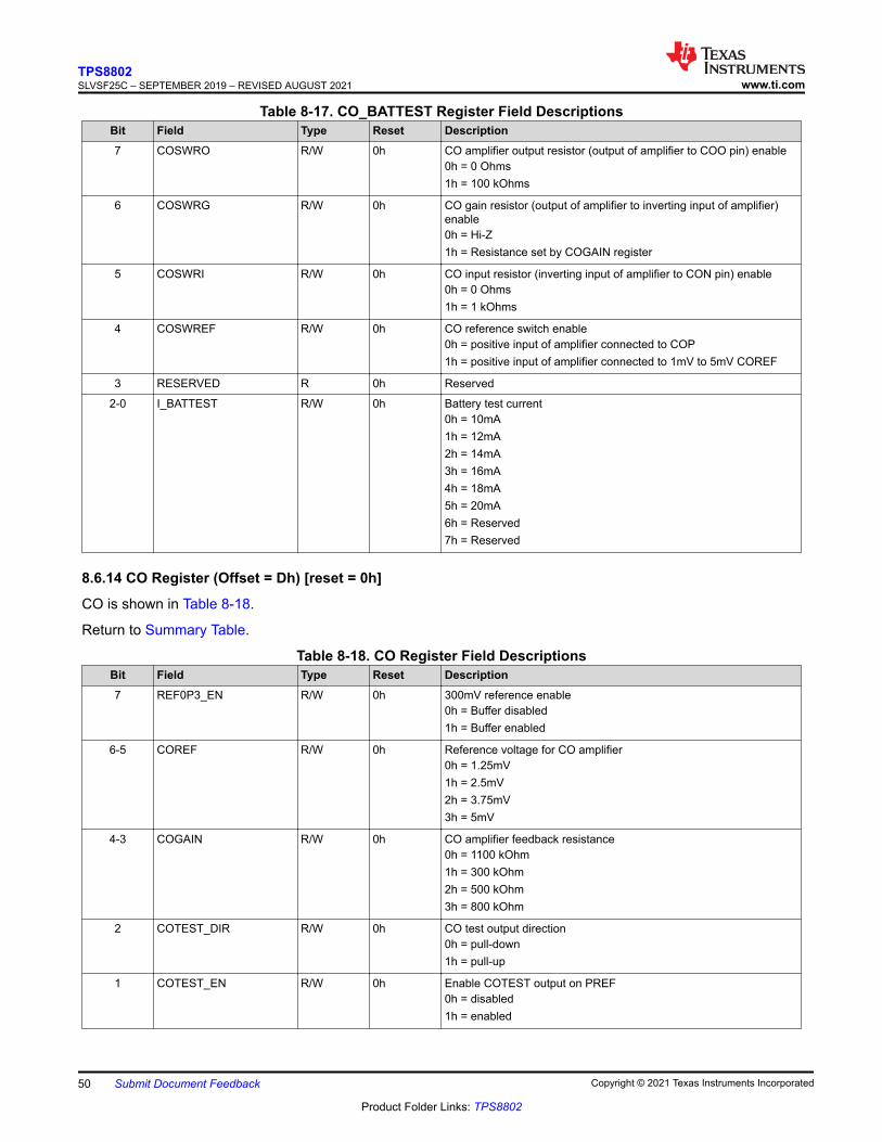
Table 8-17. CO_BATTEST Register Field DescriptionsBit Field Type Reset Description7 COSWRO R/W 0h CO amplifier output resistor (output of amplifier to COO pin) enable
0h = 0 Ohms1h = 100 kOhms
6 COSWRG R/W 0h CO gain resistor (output of amplifier to inverting input of amplifier) enable0h = Hi-Z1h = Resistance set by COGAIN register
5 COSWRI R/W 0h CO input resistor (inverting input of amplifier to CON pin) enable0h = 0 Ohms1h = 1 kOhms
4 COSWREF R/W 0h CO reference switch enable0h = positive input of amplifier connected to COP1h = positive input of amplifier connected to 1mV to 5mV COREF
3 RESERVED R 0h Reserved
2-0 I_BATTEST R/W 0h Battery test current0h = 10mA1h = 12mA2h = 14mA3h = 16mA4h = 18mA5h = 20mA6h = Reserved7h = Reserved
8.6.14 CO Register (Offset = Dh) [reset = 0h]
CO is shown in Table 8-18.
Return to Summary Table.
Table 8-18. CO Register Field DescriptionsBit Field Type Reset Description7 REF0P3_EN R/W 0h 300mV reference enable
0h = Buffer disabled1h = Buffer enabled
6-5 COREF R/W 0h Reference voltage for CO amplifier0h = 1.25mV1h = 2.5mV2h = 3.75mV3h = 5mV
4-3 COGAIN R/W 0h CO amplifier feedback resistance0h = 1100 kOhm1h = 300 kOhm2h = 500 kOhm3h = 800 kOhm
2 COTEST_DIR R/W 0h CO test output direction0h = pull-down1h = pull-up
1 COTEST_EN R/W 0h Enable COTEST output on PREF0h = disabled1h = enabled
TPS8802SLVSF25C – SEPTEMBER 2019 – REVISED AUGUST 2021 www.ti.com
50 Submit Document Feedback Copyright © 2021 Texas Instruments Incorporated
Product Folder Links: TPS8802
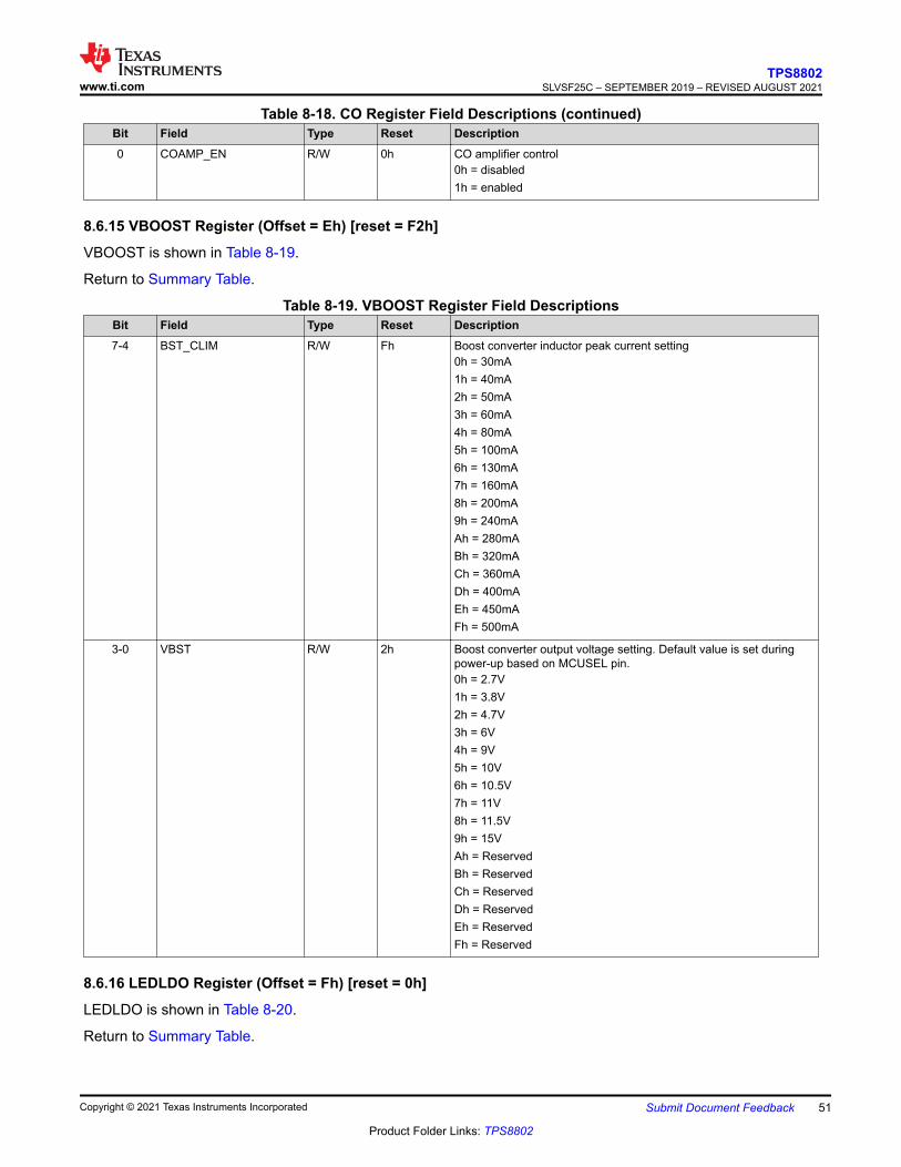
Table 8-18. CO Register Field Descriptions (continued)Bit Field Type Reset Description0 COAMP_EN R/W 0h CO amplifier control
0h = disabled1h = enabled
8.6.15 VBOOST Register (Offset = Eh) [reset = F2h]
VBOOST is shown in Table 8-19.
Return to Summary Table.
Table 8-19. VBOOST Register Field DescriptionsBit Field Type Reset Description7-4 BST_CLIM R/W Fh Boost converter inductor peak current setting
0h = 30mA1h = 40mA2h = 50mA3h = 60mA4h = 80mA5h = 100mA6h = 130mA7h = 160mA8h = 200mA9h = 240mAAh = 280mABh = 320mACh = 360mADh = 400mAEh = 450mAFh = 500mA
3-0 VBST R/W 2h Boost converter output voltage setting. Default value is set during power-up based on MCUSEL pin.0h = 2.7V1h = 3.8V2h = 4.7V3h = 6V4h = 9V5h = 10V6h = 10.5V7h = 11V8h = 11.5V9h = 15VAh = ReservedBh = ReservedCh = ReservedDh = ReservedEh = ReservedFh = Reserved
8.6.16 LEDLDO Register (Offset = Fh) [reset = 0h]
LEDLDO is shown in Table 8-20.
Return to Summary Table.
www.ti.comTPS8802
SLVSF25C – SEPTEMBER 2019 – REVISED AUGUST 2021
Copyright © 2021 Texas Instruments Incorporated Submit Document Feedback 51
Product Folder Links: TPS8802
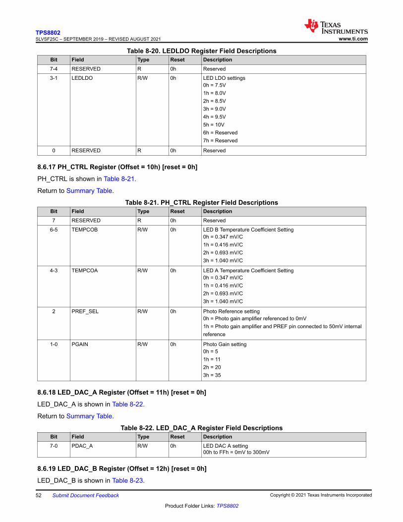
Table 8-20. LEDLDO Register Field DescriptionsBit Field Type Reset Description7-4 RESERVED R 0h Reserved
3-1 LEDLDO R/W 0h LED LDO settings0h = 7.5V1h = 8.0V2h = 8.5V3h = 9.0V4h = 9.5V5h = 10V6h = Reserved7h = Reserved
0 RESERVED R 0h Reserved
8.6.17 PH_CTRL Register (Offset = 10h) [reset = 0h]
PH_CTRL is shown in Table 8-21.
Return to Summary Table.
Table 8-21. PH_CTRL Register Field DescriptionsBit Field Type Reset Description7 RESERVED R 0h Reserved
6-5 TEMPCOB R/W 0h LED B Temperature Coefficient Setting0h = 0.347 mV/C1h = 0.416 mV/C2h = 0.693 mV/C3h = 1.040 mV/C
4-3 TEMPCOA R/W 0h LED A Temperature Coefficient Setting0h = 0.347 mV/C1h = 0.416 mV/C2h = 0.693 mV/C3h = 1.040 mV/C
2 PREF_SEL R/W 0h Photo Reference setting0h = Photo gain amplifier referenced to 0mV1h = Photo gain amplifier and PREF pin connected to 50mV internal reference
1-0 PGAIN R/W 0h Photo Gain setting0h = 51h = 112h = 203h = 35
8.6.18 LED_DAC_A Register (Offset = 11h) [reset = 0h]
LED_DAC_A is shown in Table 8-22.
Return to Summary Table.
Table 8-22. LED_DAC_A Register Field DescriptionsBit Field Type Reset Description7-0 PDAC_A R/W 0h LED DAC A setting
00h to FFh = 0mV to 300mV
8.6.19 LED_DAC_B Register (Offset = 12h) [reset = 0h]
LED_DAC_B is shown in Table 8-23.
TPS8802SLVSF25C – SEPTEMBER 2019 – REVISED AUGUST 2021 www.ti.com
52 Submit Document Feedback Copyright © 2021 Texas Instruments Incorporated
Product Folder Links: TPS8802
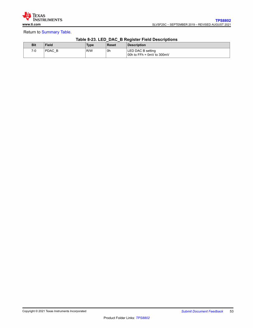
Return to Summary Table.
Table 8-23. LED_DAC_B Register Field DescriptionsBit Field Type Reset Description7-0 PDAC_B R/W 0h LED DAC B setting
00h to FFh = 0mV to 300mV
www.ti.comTPS8802
SLVSF25C – SEPTEMBER 2019 – REVISED AUGUST 2021
Copyright © 2021 Texas Instruments Incorporated Submit Document Feedback 53
Product Folder Links: TPS8802
9 Application and ImplementationNote
Information in the following applications sections is not part of the TI component specification, and TI does not warrant its accuracy or completeness. TI’s customers are responsible for determining suitability of components for their purposes, as well as validating and testing their design implementation to confirm system functionality.
9.1 Application InformationThe TPS8802 supports a variety of smoke alarm platforms:
• single-wave or dual-wave photoelectric smoke and CO detection• 3-V battery, 9-V battery, or AC/DC supply with battery backup• tone or voice alarm
TPS8802SLVSF25C – SEPTEMBER 2019 – REVISED AUGUST 2021 www.ti.com
54 Submit Document Feedback Copyright © 2021 Texas Instruments Incorporated
Product Folder Links: TPS8802
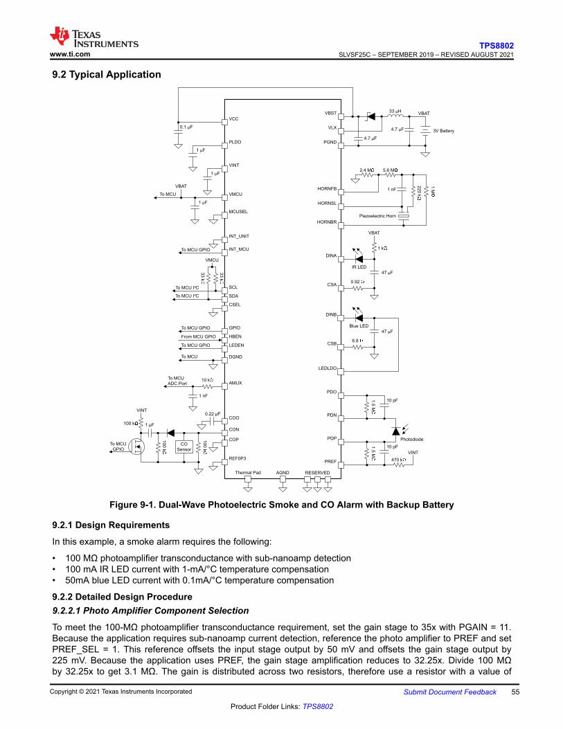
9.2 Typical Application
MCUSEL
VMCU
VINT
PLDO
VCC
VBST
VLX
INT_UNIT
INT_MCU
SCL
SDA
CSEL
GPIO
HBEN
LEDEN
DGND
AMUX
COO
CON
COP
REF0P3
HORNFB
HORNSL
HORNBR
PGND
PDP
PDN
PDO
PREF
DINA
CSA
2.4 M 5.6 M
22
0 k
1 M
47 μF
IR LED
0.92
3V Battery
1 μF
1 μF
1 nF
4.7 μF
4.7 μF
33 μH
0.1 μF
1 μF
To MCU
To MCU I²C
To MCU I²C
To MCU GPIO
To MCU GPIO
From MCU GPIO
To MCU GPIO
To MCU
ADC Port
CO
Sensor
1.5
M
10 pF
1.5
M
10 pF
Photodiode
10 k
1 nF
AGND RESERVED
DINB
CSB
47 μF
Blue LED
6.8
Piezoelectric Horn
LEDLDO
10
0 k
To MCU
Thermal Pad
VBAT
33
k
33
k
VMCU
0.22 µF
10
0 k
100 k
VINT
1 µF
To MCU
GPIO
470 k
VINT
VBAT
VBAT
1 k
Figure 9-1. Dual-Wave Photoelectric Smoke and CO Alarm with Backup Battery
9.2.1 Design Requirements
In this example, a smoke alarm requires the following:
• 100 MΩ photoamplifier transconductance with sub-nanoamp detection• 100 mA IR LED current with 1-mA/°C temperature compensation• 50mA blue LED current with 0.1mA/°C temperature compensation
9.2.2 Detailed Design Procedure9.2.2.1 Photo Amplifier Component Selection
To meet the 100-MΩ photoamplifier transconductance requirement, set the gain stage to 35x with PGAIN = 11. Because the application requires sub-nanoamp current detection, reference the photo amplifier to PREF and set PREF_SEL = 1. This reference offsets the input stage output by 50 mV and offsets the gain stage output by 225 mV. Because the application uses PREF, the gain stage amplification reduces to 32.25x. Divide 100 MΩ by 32.25x to get 3.1 MΩ. The gain is distributed across two resistors, therefore use a resistor with a value of
www.ti.comTPS8802
SLVSF25C – SEPTEMBER 2019 – REVISED AUGUST 2021
Copyright © 2021 Texas Instruments Incorporated Submit Document Feedback 55
Product Folder Links: TPS8802
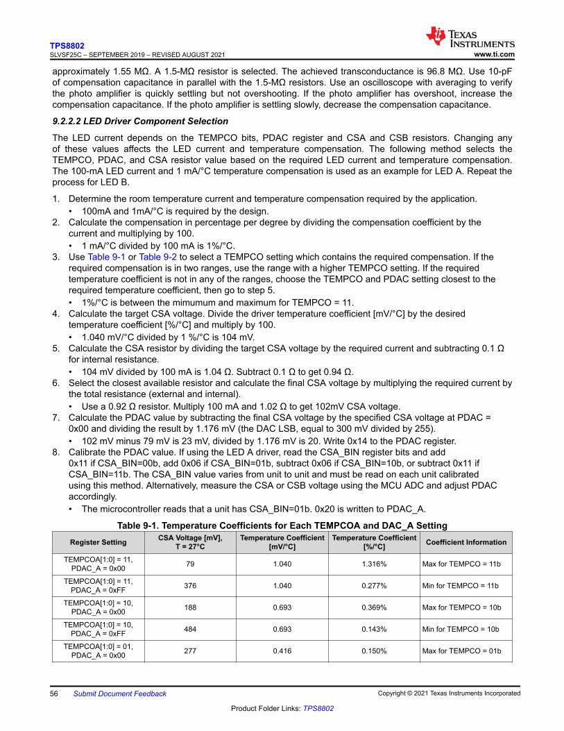
approximately 1.55 MΩ. A 1.5-MΩ resistor is selected. The achieved transconductance is 96.8 MΩ. Use 10-pF of compensation capacitance in parallel with the 1.5-MΩ resistors. Use an oscilloscope with averaging to verify the photo amplifier is quickly settling but not overshooting. If the photo amplifier has overshoot, increase the compensation capacitance. If the photo amplifier is settling slowly, decrease the compensation capacitance.
9.2.2.2 LED Driver Component Selection
The LED current depends on the TEMPCO bits, PDAC register and CSA and CSB resistors. Changing any of these values affects the LED current and temperature compensation. The following method selects the TEMPCO, PDAC, and CSA resistor value based on the required LED current and temperature compensation. The 100-mA LED current and 1 mA/°C temperature compensation is used as an example for LED A. Repeat the process for LED B.
1. Determine the room temperature current and temperature compensation required by the application.• 100mA and 1mA/°C is required by the design.
2. Calculate the compensation in percentage per degree by dividing the compensation coefficient by the current and multiplying by 100.• 1 mA/°C divided by 100 mA is 1%/°C.
3. Use Table 9-1 or Table 9-2 to select a TEMPCO setting which contains the required compensation. If the required compensation is in two ranges, use the range with a higher TEMPCO setting. If the required temperature coefficient is not in any of the ranges, choose the TEMPCO and PDAC setting closest to the required temperature coefficient, then go to step 5.• 1%/°C is between the mimumum and maximum for TEMPCO = 11.
4. Calculate the target CSA voltage. Divide the driver temperature coefficient [mV/°C] by the desired temperature coefficient [%/°C] and multiply by 100.• 1.040 mV/°C divided by 1 %/°C is 104 mV.
5. Calculate the CSA resistor by dividing the target CSA voltage by the required current and subtracting 0.1 Ω for internal resistance.• 104 mV divided by 100 mA is 1.04 Ω. Subtract 0.1 Ω to get 0.94 Ω.
6. Select the closest available resistor and calculate the final CSA voltage by multiplying the required current by the total resistance (external and internal).• Use a 0.92 Ω resistor. Multiply 100 mA and 1.02 Ω to get 102mV CSA voltage.
7. Calculate the PDAC value by subtracting the final CSA voltage by the specified CSA voltage at PDAC = 0x00 and dividing the result by 1.176 mV (the DAC LSB, equal to 300 mV divided by 255).• 102 mV minus 79 mV is 23 mV, divided by 1.176 mV is 20. Write 0x14 to the PDAC register.
8. Calibrate the PDAC value. If using the LED A driver, read the CSA_BIN register bits and add 0x11 if CSA_BIN=00b, add 0x06 if CSA_BIN=01b, subtract 0x06 if CSA_BIN=10b, or subtract 0x11 if CSA_BIN=11b. The CSA_BIN value varies from unit to unit and must be read on each unit calibrated using this method. Alternatively, measure the CSA or CSB voltage using the MCU ADC and adjust PDAC accordingly.• The microcontroller reads that a unit has CSA_BIN=01b. 0x20 is written to PDAC_A.
Table 9-1. Temperature Coefficients for Each TEMPCOA and DAC_A SettingRegister Setting CSA Voltage [mV],
T = 27°CTemperature Coefficient
[mV/°C]Temperature Coefficient
[%/°C] Coefficient Information
TEMPCOA[1:0] = 11, PDAC_A = 0x00 79 1.040 1.316% Max for TEMPCO = 11b
TEMPCOA[1:0] = 11, PDAC_A = 0xFF 376 1.040 0.277% Min for TEMPCO = 11b
TEMPCOA[1:0] = 10, PDAC_A = 0x00 188 0.693 0.369% Max for TEMPCO = 10b
TEMPCOA[1:0] = 10, PDAC_A = 0xFF 484 0.693 0.143% Min for TEMPCO = 10b
TEMPCOA[1:0] = 01, PDAC_A = 0x00 277 0.416 0.150% Max for TEMPCO = 01b
TPS8802SLVSF25C – SEPTEMBER 2019 – REVISED AUGUST 2021 www.ti.com
56 Submit Document Feedback Copyright © 2021 Texas Instruments Incorporated
Product Folder Links: TPS8802
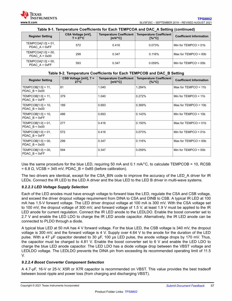
Table 9-1. Temperature Coefficients for Each TEMPCOA and DAC_A Setting (continued)Register Setting CSA Voltage [mV],
T = 27°CTemperature Coefficient
[mV/°C]Temperature Coefficient
[%/°C] Coefficient Information
TEMPCOA[1:0] = 01, PDAC_A = 0xFF 572 0.416 0.073% Min for TEMPCO = 01b
TEMPCOA[1:0] = 00, PDAC_A = 0x00 299 0.347 0.116% Max for TEMPCO = 00b
TEMPCOA[1:0] = 00, PDAC_A = 0xFF 593 0.347 0.059% Min for TEMPCO = 00b
Table 9-2. Temperature Coefficients for Each TEMPCOB and DAC_B SettingRegister Setting CSB Voltage [mV], T =
27°CTemperature Coefficient
[mV/°C]Temperature Coefficient
[%/°C] Coefficient Information
TEMPCOB[1:0] = 11, PDAC_B = 0x00
81 1.040 1.284% Max for TEMPCO = 11b
TEMPCOB[1:0] = 11, PDAC_B = 0xFF
379 1.040 0.272% Min for TEMPCO = 11b
TEMPCOB[1:0] = 10, PDAC_B = 0x00
189 0.693 0.369% Max for TEMPCO = 10b
TEMPCOB[1:0] = 10, PDAC_B = 0xFF
486 0.693 0.143% Min for TEMPCO = 10b
TEMPCOB[1:0] = 01, PDAC_B = 0x00
277 0.416 0.150% Max for TEMPCO = 01b
TEMPCOB[1:0] = 01, PDAC_B = 0xFF
572 0.416 0.073% Min for TEMPCO = 01b
TEMPCOB[1:0] = 00, PDAC_B = 0x00
299 0.347 0.116% Max for TEMPCO = 00b
TEMPCOB[1:0] = 00, PDAC_B = 0xFF
594 0.347 0.059% Min for TEMPCO = 00b
Use the same procedure for the blue LED, requiring 50 mA and 0.1 mA/°C, to calculate TEMPCOB = 10, RCSB = 6.8 Ω, VCSB = 345 mV, PDAC_B = 0x85 (before calibration).
The two drivers are identical, except for the CSA_BIN code to improve the accuracy of the LED_A driver for IR LEDs. Connect the IR LED to the LED A driver and the blue LED to the LED B driver in multi-wave systems.
9.2.2.3 LED Voltage Supply Selection
Each of the LED anodes must have enough voltage to forward bias the LED, regulate the CSA and CSB voltage, and exceed the driver dropout voltage requirement from DINA to CSA and DINB to CSB. A typical IR LED at 100 mA has 1.5-V forward voltage. The LED driver dropout voltage at 100 mA is 300 mV. With the CSA voltage set to 100 mV, the dropout voltage of 300 mV, and forward voltage of 1.5 V, at least 1.9 V must be applied to the IR LED anode for current regulation. Connect the IR LED anode to the LEDLDO. Enable the boost converter set to 2.7 V and enable the LED LDO to charge the IR LED anode capacitor. Alternatively, the IR LED anode can be connected to PLDO through a diode.
A typical blue LED at 50 mA has 4 V forward voltage. For the blue LED, the CSB voltage is 340 mV, the dropout voltage is 300 mV, and the forward voltage is 4 V. Supply over 4.64 V to the anode for the duration of the LED pulse. With a 47 µF capacitor derated to 30 µF, 100 µs LED pulse, the anode voltage drops by 170 mV. Thus, the capacitor must be charged to 4.81 V. Enable the boost converter set to 6 V and enable the LED LDO to charge the blue LED anode capacitor. The LED LDO has a diode voltage drop between the VBST voltage and LEDLDO voltage. The LEDLDO prevents the DINA pin from exceeding its recommended operating limit of 11.5 V.
9.2.2.4 Boost Converter Component Selection
A 4.7-μF, 16-V or 25-V, X5R or X7R capacitor is recommended on VBST. This value provides the best tradeoff between boost ripple and power loss (from charging and discharging VBST).
www.ti.comTPS8802
SLVSF25C – SEPTEMBER 2019 – REVISED AUGUST 2021
Copyright © 2021 Texas Instruments Incorporated Submit Document Feedback 57
Product Folder Links: TPS8802
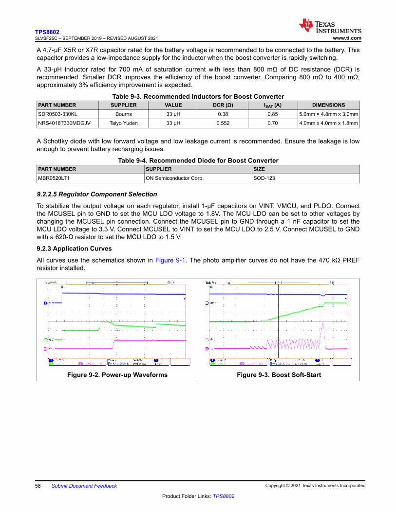
A 4.7-μF X5R or X7R capacitor rated for the battery voltage is recommended to be connected to the battery. This capacitor provides a low-impedance supply for the inductor when the boost converter is rapidly switching.
A 33-μH inductor rated for 700 mA of saturation current with less than 800 mΩ of DC resistance (DCR) is recommended. Smaller DCR improves the efficiency of the boost converter. Comparing 800 mΩ to 400 mΩ, approximately 3% efficiency improvement is expected.
Table 9-3. Recommended Inductors for Boost ConverterPART NUMBER SUPPLIER VALUE DCR (Ω) ISAT (A) DIMENSIONSSDR0503-330KL Bourns 33 μH 0.38 0.85 5.0mm × 4.8mm x 3.0mm
NRS4018T330MDGJV Taiyo Yuden 33 μH 0.552 0.70 4.0mm x 4.0mm x 1.8mm
A Schottky diode with low forward voltage and low leakage current is recommended. Ensure the leakage is low enough to prevent battery recharging issues.
Table 9-4. Recommended Diode for Boost ConverterPART NUMBER SUPPLIER SIZEMBR0520LT1 ON Semiconductor Corp. SOD-123
9.2.2.5 Regulator Component Selection
To stabilize the output voltage on each regulator, install 1-µF capacitors on VINT, VMCU, and PLDO. Connect the MCUSEL pin to GND to set the MCU LDO voltage to 1.8V. The MCU LDO can be set to other voltages by changing the MCUSEL pin connection. Connect the MCUSEL pin to GND through a 1 nF capacitor to set the MCU LDO voltage to 3.3 V. Connect MCUSEL to VINT to set the MCU LDO to 2.5 V. Connect MCUSEL to GND with a 620-Ω resistor to set the MCU LDO to 1.5 V.
9.2.3 Application Curves
All curves use the schematics shown in Figure 9-1. The photo amplifier curves do not have the 470 kΩ PREF resistor installed.
Figure 9-2. Power-up Waveforms Figure 9-3. Boost Soft-Start
TPS8802SLVSF25C – SEPTEMBER 2019 – REVISED AUGUST 2021 www.ti.com
58 Submit Document Feedback Copyright © 2021 Texas Instruments Incorporated
Product Folder Links: TPS8802
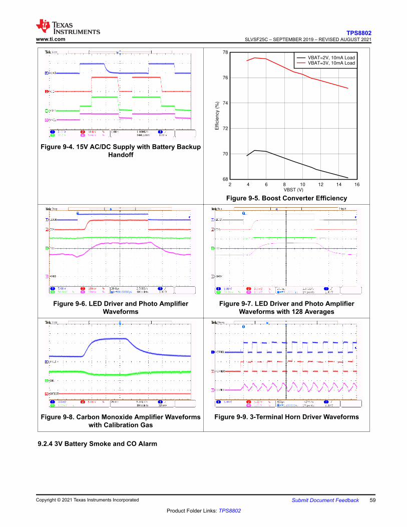
Figure 9-4. 15V AC/DC Supply with Battery Backup Handoff
VBST (V)
Effic
ien
cy (
%)
2 4 6 8 10 12 14 1668
70
72
74
76
78VBAT=2V, 10mA LoadVBAT=3V, 10mA Load
Figure 9-5. Boost Converter Efficiency
Figure 9-6. LED Driver and Photo Amplifier Waveforms
Figure 9-7. LED Driver and Photo Amplifier Waveforms with 128 Averages
Figure 9-8. Carbon Monoxide Amplifier Waveforms with Calibration Gas
Figure 9-9. 3-Terminal Horn Driver Waveforms
9.2.4 3V Battery Smoke and CO Alarm
www.ti.comTPS8802
SLVSF25C – SEPTEMBER 2019 – REVISED AUGUST 2021
Copyright © 2021 Texas Instruments Incorporated Submit Document Feedback 59
Product Folder Links: TPS8802
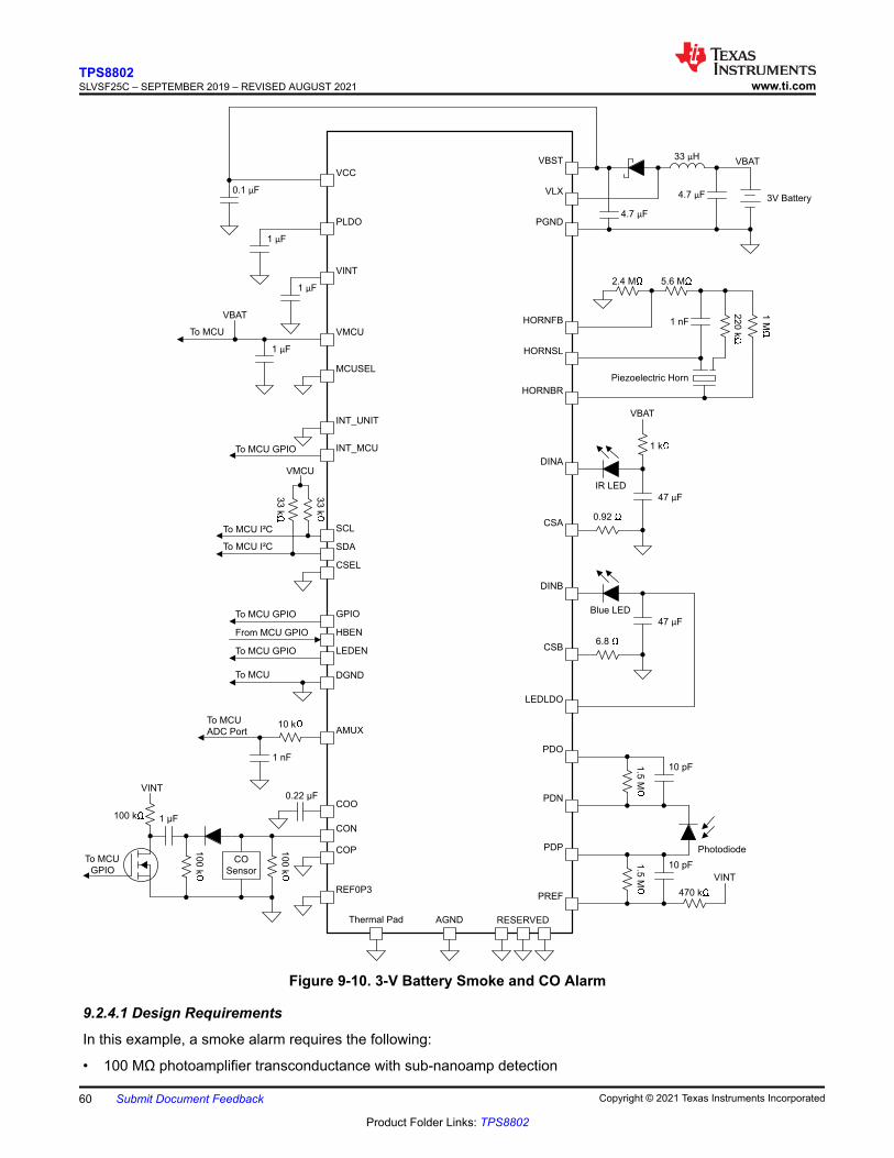
MCUSEL
VMCU
VINT
PLDO
VCC
VBST
VLX
INT_UNIT
INT_MCU
SCL
SDA
CSEL
GPIO
HBEN
LEDEN
DGND
AMUX
COO
CON
COP
REF0P3
HORNFB
HORNSL
HORNBR
PGND
PDP
PDN
PDO
PREF
DINA
CSA
2.4 M 5.6 M
220 k
1 M
47 μF
IR LED
0.92
3V Battery
1 μF
1 μF
1 nF
4.7 μF
4.7 μF
33 μH
0.1 μF
1 μF
To MCU
To MCU I²C
To MCU I²C
To MCU GPIO
To MCU GPIO
From MCU GPIO
To MCU GPIO
To MCU
ADC Port
CO
Sensor
1.5
M
10 pF
1.5
M
10 pF
Photodiode
10 k
1 nF
AGND RESERVED
DINB
CSB
47 μF
Blue LED
6.8
Piezoelectric Horn
LEDLDO
100 k
To MCU
Thermal Pad
VBAT
33 k
33 k
VMCU
0.22 µF
100 k
100 k
VINT
1 µF
To MCU
GPIO
470 k
VINT
VBAT
VBAT
1 k
Figure 9-10. 3-V Battery Smoke and CO Alarm
9.2.4.1 Design Requirements
In this example, a smoke alarm requires the following:
• 100 MΩ photoamplifier transconductance with sub-nanoamp detection
TPS8802SLVSF25C – SEPTEMBER 2019 – REVISED AUGUST 2021 www.ti.com
60 Submit Document Feedback Copyright © 2021 Texas Instruments Incorporated
Product Folder Links: TPS8802
• 100mA IR LED current with 1mA/°C temperature compensation• 50mA blue LED current with 0.1mA/°C temperature compensation• 10-year battery life with 3V lithium primary battery
9.2.4.2 Detailed Design Procedure
In this application, a 3V battery is the only power source. The 3V battery is used to directly power the IR LED and the MCU, saving power. The MCU LDO can be disabled after power-up. Ensure the MCU and IR LED can operate over the range of voltages supplied by the battery.
www.ti.comTPS8802
SLVSF25C – SEPTEMBER 2019 – REVISED AUGUST 2021
Copyright © 2021 Texas Instruments Incorporated Submit Document Feedback 61
Product Folder Links: TPS8802
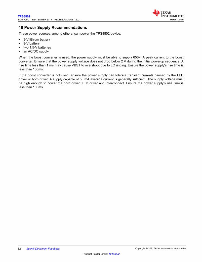
10 Power Supply RecommendationsThese power sources, among others, can power the TPS8802 device:
• 3-V lithium battery• 9-V battery• two 1.5-V batteries• an AC/DC supply
When the boost converter is used, the power supply must be able to supply 650-mA peak current to the boost converter. Ensure that the power supply voltage does not drop below 2 V during the initial powerup sequence. A rise time less than 1 ms may cause VBST to overshoot due to LC ringing. Ensure the power supply's rise time is less than 100ms.
If the boost converter is not used, ensure the power supply can tolerate transient currents caused by the LED driver or horn driver. A supply capable of 50 mA average current is generally sufficient. The supply voltage must be high enough to power the horn driver, LED driver and interconnect. Ensure the power supply's rise time is less than 100ms.
TPS8802SLVSF25C – SEPTEMBER 2019 – REVISED AUGUST 2021 www.ti.com
62 Submit Document Feedback Copyright © 2021 Texas Instruments Incorporated
Product Folder Links: TPS8802
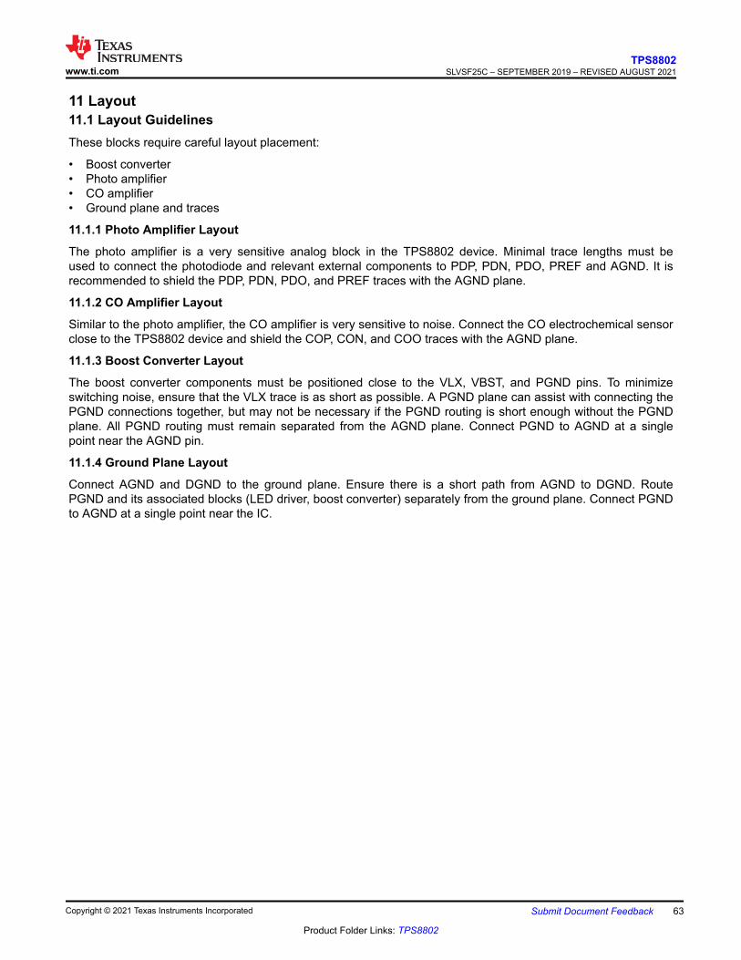
11 Layout11.1 Layout GuidelinesThese blocks require careful layout placement:
• Boost converter• Photo amplifier• CO amplifier• Ground plane and traces
11.1.1 Photo Amplifier Layout
The photo amplifier is a very sensitive analog block in the TPS8802 device. Minimal trace lengths must be used to connect the photodiode and relevant external components to PDP, PDN, PDO, PREF and AGND. It is recommended to shield the PDP, PDN, PDO, and PREF traces with the AGND plane.
11.1.2 CO Amplifier Layout
Similar to the photo amplifier, the CO amplifier is very sensitive to noise. Connect the CO electrochemical sensor close to the TPS8802 device and shield the COP, CON, and COO traces with the AGND plane.
11.1.3 Boost Converter Layout
The boost converter components must be positioned close to the VLX, VBST, and PGND pins. To minimize switching noise, ensure that the VLX trace is as short as possible. A PGND plane can assist with connecting the PGND connections together, but may not be necessary if the PGND routing is short enough without the PGND plane. All PGND routing must remain separated from the AGND plane. Connect PGND to AGND at a single point near the AGND pin.
11.1.4 Ground Plane Layout
Connect AGND and DGND to the ground plane. Ensure there is a short path from AGND to DGND. Route PGND and its associated blocks (LED driver, boost converter) separately from the ground plane. Connect PGND to AGND at a single point near the IC.
www.ti.comTPS8802
SLVSF25C – SEPTEMBER 2019 – REVISED AUGUST 2021
Copyright © 2021 Texas Instruments Incorporated Submit Document Feedback 63
Product Folder Links: TPS8802
11.2 Layout Example
Figure 11-1. Photo Amplifier Layout
TPS8802SLVSF25C – SEPTEMBER 2019 – REVISED AUGUST 2021 www.ti.com
64 Submit Document Feedback Copyright © 2021 Texas Instruments Incorporated
Product Folder Links: TPS8802
Figure 11-2. CO Amplifier Layout
www.ti.comTPS8802
SLVSF25C – SEPTEMBER 2019 – REVISED AUGUST 2021
Copyright © 2021 Texas Instruments Incorporated Submit Document Feedback 65
Product Folder Links: TPS8802
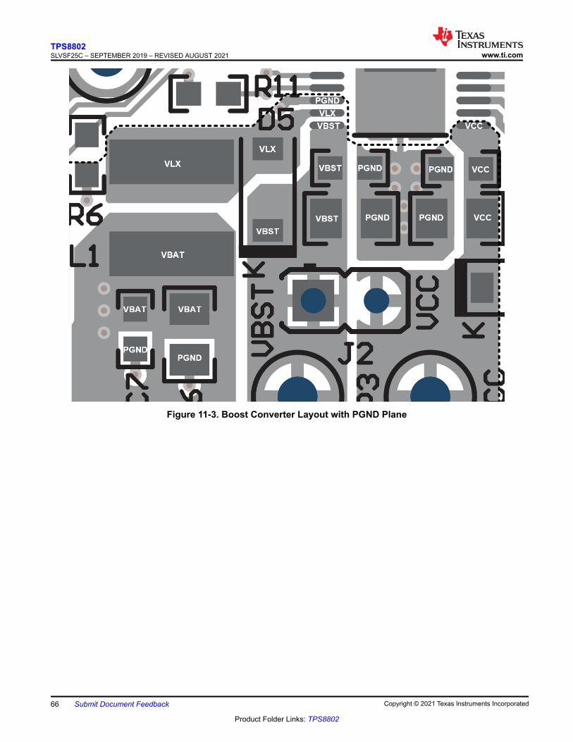
Figure 11-3. Boost Converter Layout with PGND Plane
TPS8802SLVSF25C – SEPTEMBER 2019 – REVISED AUGUST 2021 www.ti.com
66 Submit Document Feedback Copyright © 2021 Texas Instruments Incorporated
Product Folder Links: TPS8802
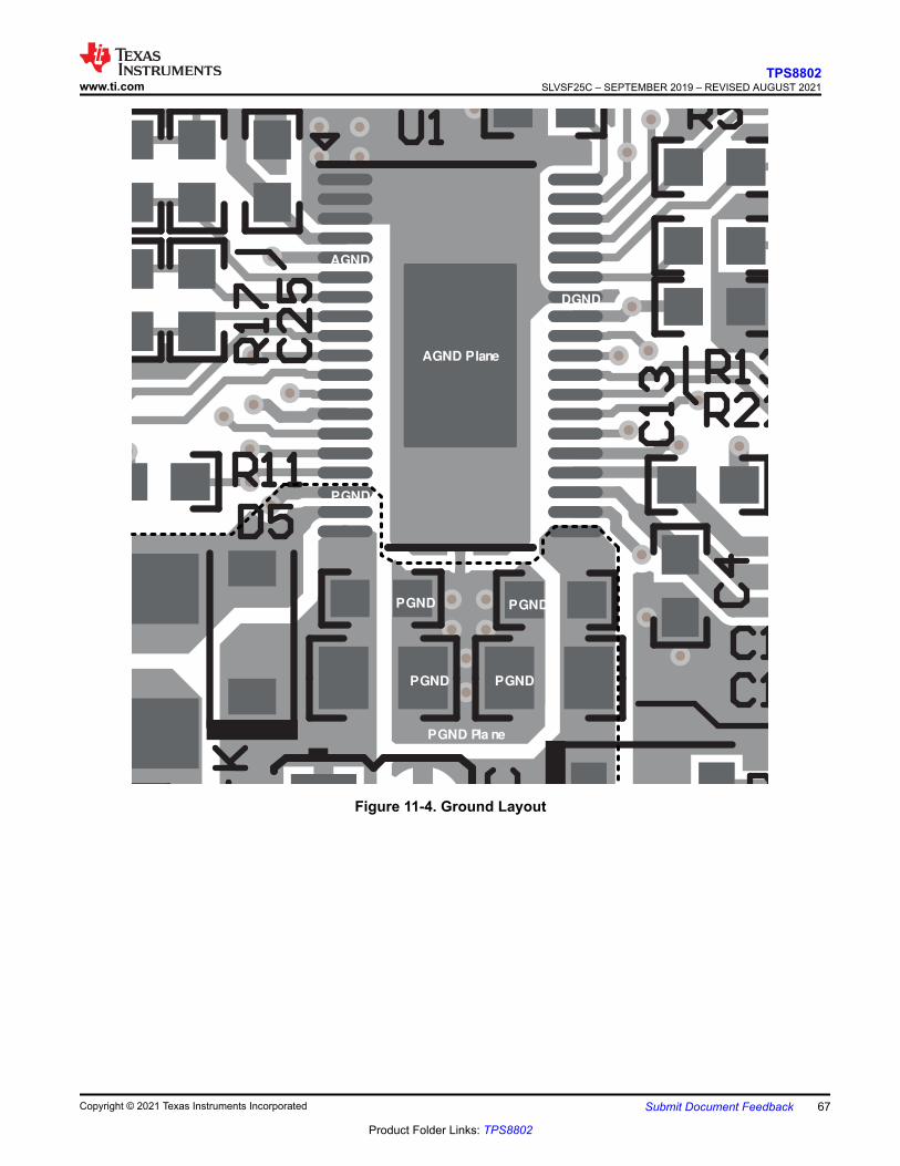
PGND
PGND
AGND
PGNDPGND
PGND
DGND
AGND Plane
PGND Pla ne
Figure 11-4. Ground Layout
www.ti.comTPS8802
SLVSF25C – SEPTEMBER 2019 – REVISED AUGUST 2021
Copyright © 2021 Texas Instruments Incorporated Submit Document Feedback 67
Product Folder Links: TPS8802
12 Device and Documentation Support12.1 Receiving Notification of Documentation UpdatesTo receive notification of documentation updates, navigate to the device product folder on ti.com. Click on Subscribe to updates to register and receive a weekly digest of any product information that has changed. For change details, review the revision history included in any revised document.
12.2 Support ResourcesTI E2E™ support forums are an engineer's go-to source for fast, verified answers and design help — straight from the experts. Search existing answers or ask your own question to get the quick design help you need.
Linked content is provided "AS IS" by the respective contributors. They do not constitute TI specifications and do not necessarily reflect TI's views; see TI's Terms of Use.
12.3 TrademarksTI E2E™ is a trademark of Texas Instruments.All trademarks are the property of their respective owners.12.4 Electrostatic Discharge Caution
This integrated circuit can be damaged by ESD. Texas Instruments recommends that all integrated circuits be handled with appropriate precautions. Failure to observe proper handling and installation procedures can cause damage.ESD damage can range from subtle performance degradation to complete device failure. Precision integrated circuits may be more susceptible to damage because very small parametric changes could cause the device not to meet its published specifications.
12.5 GlossaryTI Glossary This glossary lists and explains terms, acronyms, and definitions.
TPS8802SLVSF25C – SEPTEMBER 2019 – REVISED AUGUST 2021 www.ti.com
68 Submit Document Feedback Copyright © 2021 Texas Instruments Incorporated
Product Folder Links: TPS8802
13 Mechanical, Packaging, and Orderable InformationThe following pages include mechanical, packaging, and orderable information. This information is the most current data available for the designated devices. This data is subject to change without notice and revision of this document. For browser-based versions of this data sheet, refer to the left-hand navigation.
www.ti.comTPS8802
SLVSF25C – SEPTEMBER 2019 – REVISED AUGUST 2021
Copyright © 2021 Texas Instruments Incorporated Submit Document Feedback 69
Product Folder Links: TPS8802
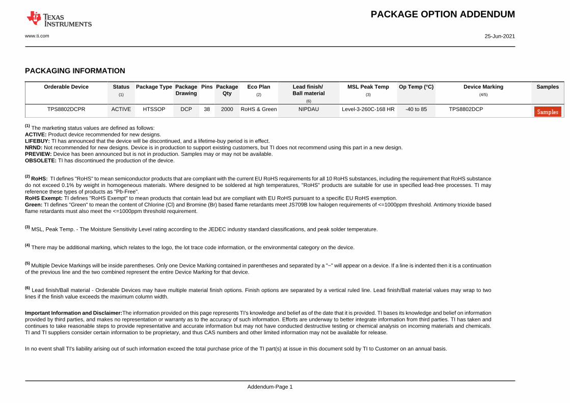
PACKAGE OPTION ADDENDUM
www.ti.com 25-Jun-2021
Addendum-Page 1
PACKAGING INFORMATION
Orderable Device Status(1)
Package Type PackageDrawing
Pins PackageQty
Eco Plan(2)
Lead finish/Ball material
(6)
MSL Peak Temp(3)
Op Temp (°C) Device Marking(4/5)
Samples
TPS8802DCPR ACTIVE HTSSOP DCP 38 2000 RoHS & Green NIPDAU Level-3-260C-168 HR -40 to 85 TPS8802DCP
(1) The marketing status values are defined as follows:ACTIVE: Product device recommended for new designs.LIFEBUY: TI has announced that the device will be discontinued, and a lifetime-buy period is in effect.NRND: Not recommended for new designs. Device is in production to support existing customers, but TI does not recommend using this part in a new design.PREVIEW: Device has been announced but is not in production. Samples may or may not be available.OBSOLETE: TI has discontinued the production of the device.
(2) RoHS: TI defines "RoHS" to mean semiconductor products that are compliant with the current EU RoHS requirements for all 10 RoHS substances, including the requirement that RoHS substancedo not exceed 0.1% by weight in homogeneous materials. Where designed to be soldered at high temperatures, "RoHS" products are suitable for use in specified lead-free processes. TI mayreference these types of products as "Pb-Free".RoHS Exempt: TI defines "RoHS Exempt" to mean products that contain lead but are compliant with EU RoHS pursuant to a specific EU RoHS exemption.Green: TI defines "Green" to mean the content of Chlorine (Cl) and Bromine (Br) based flame retardants meet JS709B low halogen requirements of <=1000ppm threshold. Antimony trioxide basedflame retardants must also meet the <=1000ppm threshold requirement.
(3) MSL, Peak Temp. - The Moisture Sensitivity Level rating according to the JEDEC industry standard classifications, and peak solder temperature.
(4) There may be additional marking, which relates to the logo, the lot trace code information, or the environmental category on the device.
(5) Multiple Device Markings will be inside parentheses. Only one Device Marking contained in parentheses and separated by a "~" will appear on a device. If a line is indented then it is a continuationof the previous line and the two combined represent the entire Device Marking for that device.
(6) Lead finish/Ball material - Orderable Devices may have multiple material finish options. Finish options are separated by a vertical ruled line. Lead finish/Ball material values may wrap to twolines if the finish value exceeds the maximum column width.
Important Information and Disclaimer:The information provided on this page represents TI's knowledge and belief as of the date that it is provided. TI bases its knowledge and belief on informationprovided by third parties, and makes no representation or warranty as to the accuracy of such information. Efforts are underway to better integrate information from third parties. TI has taken andcontinues to take reasonable steps to provide representative and accurate information but may not have conducted destructive testing or chemical analysis on incoming materials and chemicals.TI and TI suppliers consider certain information to be proprietary, and thus CAS numbers and other limited information may not be available for release.
In no event shall TI's liability arising out of such information exceed the total purchase price of the TI part(s) at issue in this document sold by TI to Customer on an annual basis.
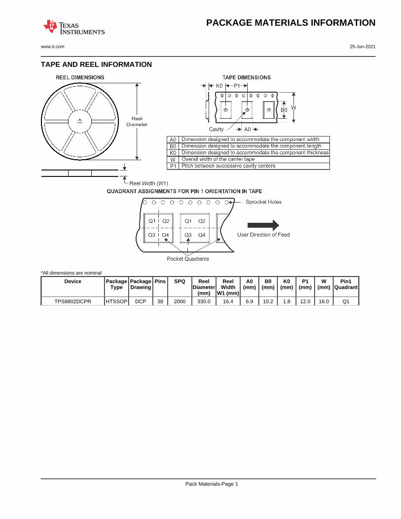
TAPE AND REEL INFORMATION
*All dimensions are nominal
Device PackageType
PackageDrawing
Pins SPQ ReelDiameter
(mm)
ReelWidth
W1 (mm)
A0(mm)
B0(mm)
K0(mm)
P1(mm)
W(mm)
Pin1Quadrant
TPS8802DCPR HTSSOP DCP 38 2000 330.0 16.4 6.9 10.2 1.8 12.0 16.0 Q1
PACKAGE MATERIALS INFORMATION
www.ti.com 25-Jun-2021
Pack Materials-Page 1
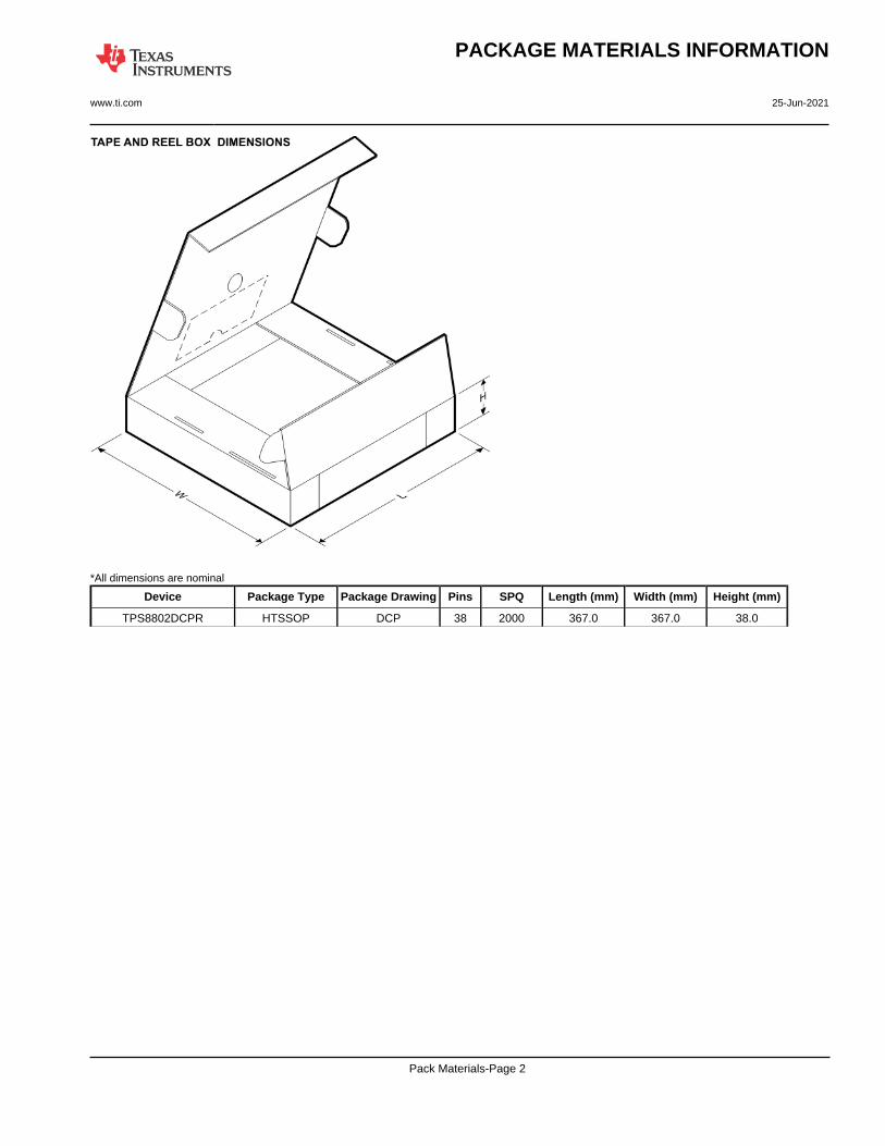
*All dimensions are nominal
Device Package Type Package Drawing Pins SPQ Length (mm) Width (mm) Height (mm)
TPS8802DCPR HTSSOP DCP 38 2000 367.0 367.0 38.0
PACKAGE MATERIALS INFORMATION
www.ti.com 25-Jun-2021
Pack Materials-Page 2
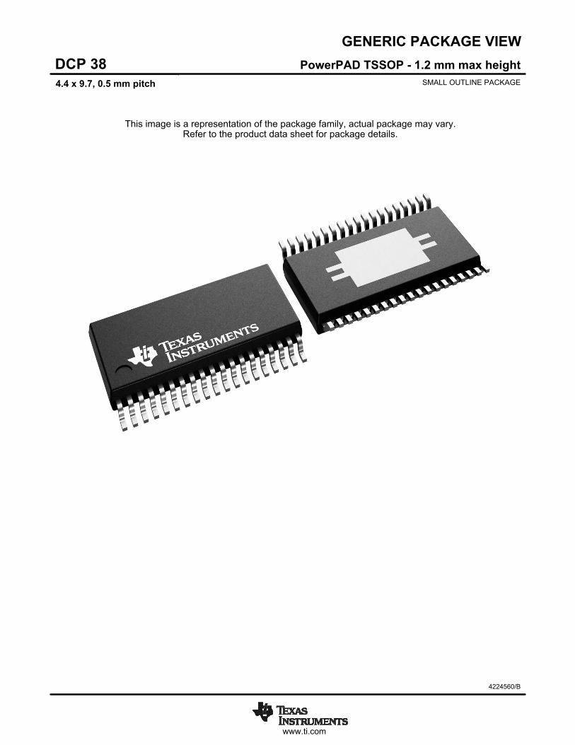
www.ti.com
GENERIC PACKAGE VIEW
This image is a representation of the package family, actual package may vary.Refer to the product data sheet for package details.
PowerPAD TSSOP - 1.2 mm max heightDCP 38SMALL OUTLINE PACKAGE4.4 x 9.7, 0.5 mm pitch
4224560/B
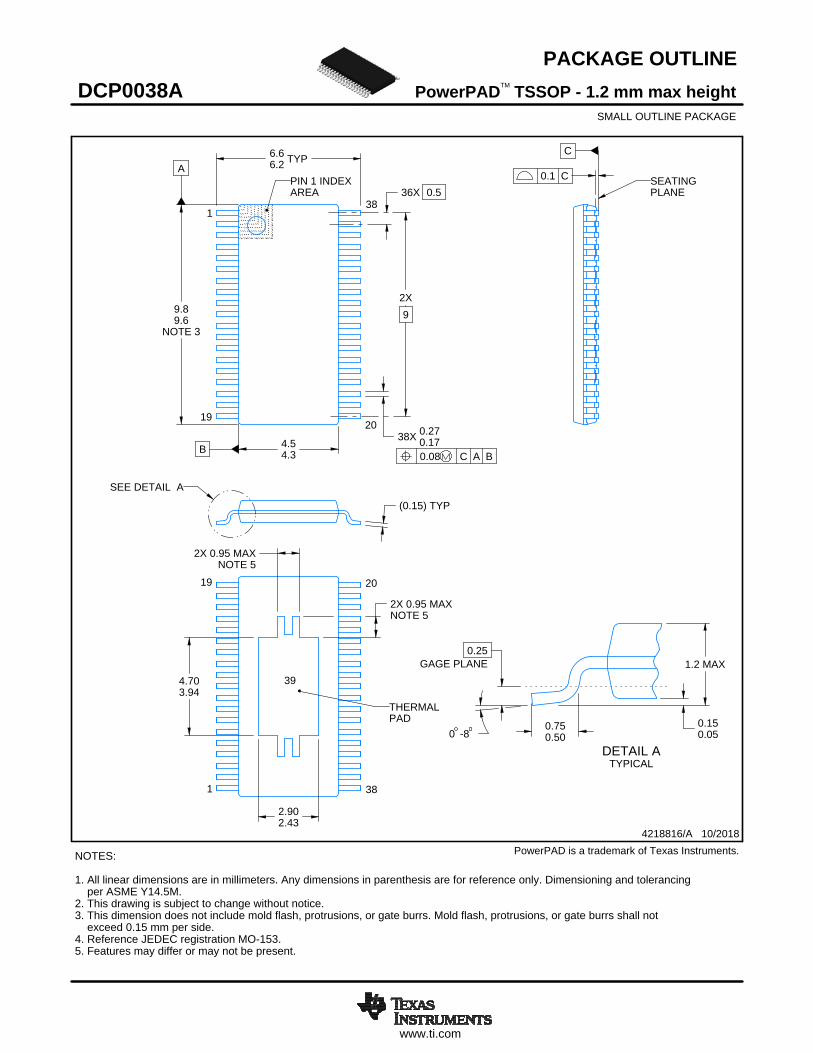
www.ti.com
PACKAGE OUTLINE
C
36X 0.5
2X9
38X 0.270.17
6.66.2 TYP
SEATINGPLANE
0.150.05
0.25GAGE PLANE
0 -8
1.2 MAX
2X 0.95 MAXNOTE 5
2X 0.95 MAXNOTE 5
4.703.94
2.902.43
B 4.54.3
A
9.89.6
NOTE 3
0.750.50
(0.15) TYP
PowerPAD TSSOP - 1.2 mm max heightDCP0038ASMALL OUTLINE PACKAGE
4218816/A 10/2018
1
1920
38
0.08 C A B
PIN 1 INDEXAREA
SEE DETAIL A
0.1 C
NOTES: 1. All linear dimensions are in millimeters. Any dimensions in parenthesis are for reference only. Dimensioning and tolerancing per ASME Y14.5M. 2. This drawing is subject to change without notice. 3. This dimension does not include mold flash, protrusions, or gate burrs. Mold flash, protrusions, or gate burrs shall not exceed 0.15 mm per side. 4. Reference JEDEC registration MO-153.5. Features may differ or may not be present.
TM
PowerPAD is a trademark of Texas Instruments.
A 20DETAIL ATYPICAL
SCALE 2.000
THERMALPAD
1
19 20
38
39
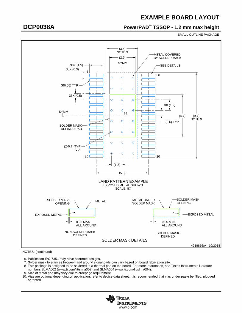
www.ti.com
EXAMPLE BOARD LAYOUT
0.05 MAXALL AROUND
0.05 MINALL AROUND
38X (1.5)38X (0.3)
36X (0.5)
(5.8)
(R0.05) TYP
(3.4)NOTE 9
(9.7)NOTE 9
( 0.2) TYPVIA
(2.9)
(4.7)
(1.2)
(0.6) TYP
3X (1.2)
PowerPAD TSSOP - 1.2 mm max heightDCP0038ASMALL OUTLINE PACKAGE
4218816/A 10/2018
NOTES: (continued) 6. Publication IPC-7351 may have alternate designs. 7. Solder mask tolerances between and around signal pads can vary based on board fabrication site. 8. This package is designed to be soldered to a thermal pad on the board. For more information, see Texas Instruments literature numbers SLMA002 (www.ti.com/lit/slma002) and SLMA004 (www.ti.com/lit/slma004). 9. Size of metal pad may vary due to creepage requirement.10. Vias are optional depending on application, refer to device data sheet. It is recommended that vias under paste be filled, plugged or tented.
TM
LAND PATTERN EXAMPLEEXPOSED METAL SHOWN
SCALE: 8X
SYMM
SYMM
1
19 20
38
METAL COVEREDBY SOLDER MASK
SOLDER MASKDEFINED PAD
SEE DETAILS
39
15.000
METALSOLDER MASKOPENING
METAL UNDERSOLDER MASK
SOLDER MASKOPENING
EXPOSED METALEXPOSED METAL
SOLDER MASK DETAILS
NON-SOLDER MASKDEFINED
SOLDER MASKDEFINED
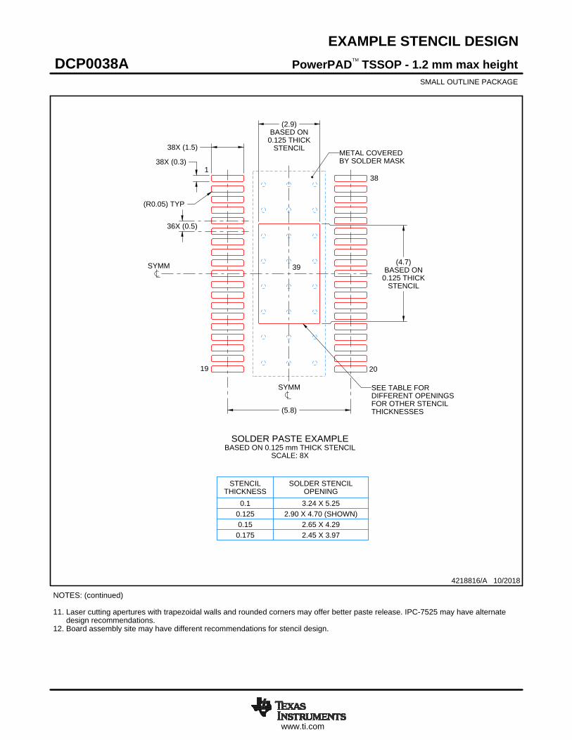
www.ti.com
EXAMPLE STENCIL DESIGN
38X (1.5)
38X (0.3)
36X (0.5)
(5.8)
(R0.05) TYP
(4.7)BASED ON
0.125 THICKSTENCIL
(2.9)BASED ON
0.125 THICKSTENCIL
PowerPAD TSSOP - 1.2 mm max heightDCP0038ASMALL OUTLINE PACKAGE
4218816/A 10/2018
2.45 X 3.970.1752.65 X 4.290.15
2.90 X 4.70 (SHOWN)0.1253.24 X 5.250.1
SOLDER STENCILOPENING
STENCILTHICKNESS
NOTES: (continued) 11. Laser cutting apertures with trapezoidal walls and rounded corners may offer better paste release. IPC-7525 may have alternate design recommendations. 12. Board assembly site may have different recommendations for stencil design.
TM
SOLDER PASTE EXAMPLEBASED ON 0.125 mm THICK STENCIL
SCALE: 8X
SYMM
SYMM
1
19 20
38
METAL COVEREDBY SOLDER MASK
SEE TABLE FORDIFFERENT OPENINGSFOR OTHER STENCILTHICKNESSES
39
IMPORTANT NOTICE AND DISCLAIMERTI PROVIDES TECHNICAL AND RELIABILITY DATA (INCLUDING DATASHEETS), DESIGN RESOURCES (INCLUDING REFERENCEDESIGNS), APPLICATION OR OTHER DESIGN ADVICE, WEB TOOLS, SAFETY INFORMATION, AND OTHER RESOURCES “AS IS”AND WITH ALL FAULTS, AND DISCLAIMS ALL WARRANTIES, EXPRESS AND IMPLIED, INCLUDING WITHOUT LIMITATION ANYIMPLIED WARRANTIES OF MERCHANTABILITY, FITNESS FOR A PARTICULAR PURPOSE OR NON-INFRINGEMENT OF THIRDPARTY INTELLECTUAL PROPERTY RIGHTS.These resources are intended for skilled developers designing with TI products. You are solely responsible for (1) selecting the appropriateTI products for your application, (2) designing, validating and testing your application, and (3) ensuring your application meets applicablestandards, and any other safety, security, or other requirements. These resources are subject to change without notice. TI grants youpermission to use these resources only for development of an application that uses the TI products described in the resource. Otherreproduction and display of these resources is prohibited. No license is granted to any other TI intellectual property right or to any third partyintellectual property right. TI disclaims responsibility for, and you will fully indemnify TI and its representatives against, any claims, damages,costs, losses, and liabilities arising out of your use of these resources.TI’s products are provided subject to TI’s Terms of Sale (https:www.ti.com/legal/termsofsale.html) or other applicable terms available eitheron ti.com or provided in conjunction with such TI products. TI’s provision of these resources does not expand or otherwise alter TI’sapplicable warranties or warranty disclaimers for TI products.IMPORTANT NOTICE
Mailing Address: Texas Instruments, Post Office Box 655303, Dallas, Texas 75265Copyright © 2021, Texas Instruments Incorporated