Embed Size (px)
Citation preview
Product
Folder
Order
Now
Technical
Documents
Tools &
Software
Support &Community
An IMPORTANT NOTICE at the end of this data sheet addresses availability, warranty, changes, use in safety-critical applications,intellectual property matters and other important disclaimers. PRODUCTION DATA.
TPS65094, TPS650940, TPS650941, TPS650942, TPS650944SWCS133B –SEPTEMBER 2015–REVISED FEBRUARY 2017
TPS65094x PMIC for Intel™ Apollo Lake Platform
1 Device Overview
1
1.1 Features1
• Wide VIN Range From 5.6 V to 21 V• Three Variable-Output Voltage Synchronous
Step-Down Controllers With D-CAP2™ Topology– 5 A for BUCK1 (VNN), 7 A for BUCK6 (VDDQ),
and 21 A for BUCK2 (VCCGI) Using ExternalFETs for Typical Applications
– I2C Dynamic Voltage Scaling (DVS) Control(0.5 V to 1.45 V in 10-mV Steps) for BUCK1 andBUCK2
– OTP-Programmable Default Output Voltage forBUCK6 (VDDQ)
• Three Variable-Output Voltage SynchronousStep-Down Converters With DCS-ControlTopology and I2C DVS Capabilities– VIN Range From 4.5 V to 5.5 V– 3 A of Output Current for BUCK3 (VCCRAM)– 2 A of Output Current for BUCK4 (V1P8A) and
BUCK5 (V1P24A) for Typical Applications
• Three LDO Regulators With Adjustable OutputVoltage– LDOA1: I2C-Selectable Output Voltage From
1.35 V to 3.3 V for up to 200 mA of OutputCurrent
– LDOA2 and LDOA3: I2C-Selectable OutputVoltage From 0.7 V to 1.5 V for up to 600 mA ofOutput Current
• VTT LDO for DDR Memory Termination• Three Load Switches With Slew Rate Control
– Up to 400 mA of Output Current With VoltageDrop Less Than 1.5% of Nominal Input Voltage
– RDSON < 96 mΩ at Input Voltage of 1.8 V• I2C Interface (Device Address 0x5E) Supports:
– Standard Mode (100 kHz)– Fast Mode (400 kHz)– Fast Mode Plus (1 MHz)
1.2 Applications• 2-, 3-, or 4-Series Cell Li-Ion Battery-Powered
Products (NVDC or Non-NVDC)• Wall-Powered Designs, Particularly From 12-V
Supply
• Tablets, Ultrabook™, and Notebook Computers• Mobile PCs and Mobile Internet Devices
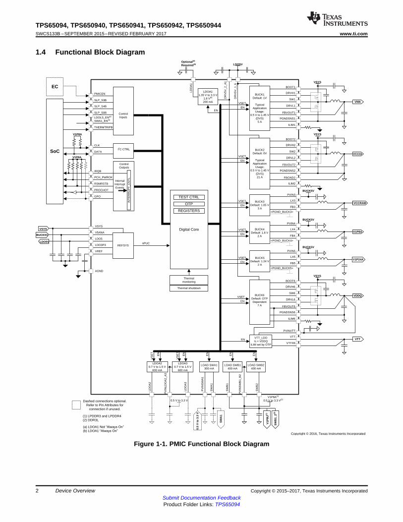
1.3 DescriptionThe TPS65094x device is a single-chip solution, power-management integrated chip (PMIC) designedspecifically for the latest Intel™ processors targeted for tablets, ultrabooks, notebooks, industrial PCs, andInternet-of-Things (IOT) applications using 2S, 3S, or 4S Li-Ion battery packs (NVDC or non-NVDC powerarchitectures), as well as wall-powered applications. The TPS65094x device is used for essential systemswith low-voltage rails merged for the smallest footprint and lowest-cost system-power solution. TheTPS65094x device provides the complete power solution based on the Intel Reference Designs. Six highlyefficient step-down voltage regulators (VRs), a sink or source LDO (VTT), and a load switch are controlledby power-up sequence logic to provide the proper power rails, sequencing, and protection—includingDDR3 and DDR4 memory power. The two regulators (BUCK1 and BUCK2) support dynamic voltagescaling (DVS) for maximum efficiency—including support for Connected Standby. The high-frequency VRsuse small inductors and capacitors to achieve a small solution size. An I2C interface allows simple controlby an embedded controller (EC) or by a system on chip (SoC). The PMIC comes in an 8-mm × 8-mmsingle-row VQFN package with a thermal pad for good thermal dissipation and ease of board routing.
(1) For more information, see the Mechanical Packaging and Orderable Information section.
Device Information (1)
PART NUMBER PACKAGE BODY SIZE (NOM)TPS65094x VQFN (64) 8.00 mm × 8.00 mm
IRQB
ControlOutputs
REFSYS
REGISTERS
Digital Core
INT
ER
RU
PT
_CN
TL
Thermalmonitoring
Thermal shutdown
OTP
TEST CTRL
I2C CTRL
SLP_S0B
PCH_PWROK
RSMRSTB
PROCHOT
InternalInterrupt Events
<PGND_BUCK3>
BUCK3Default: 1.05 V
3 A
VREF
BUCK1Default: 1V
Typical Application
Usage:0.5 V to 1.45 V
(DVS)5 A
VSYS
LDOA20.7 V to 1.5 V
600 mA
ControlInputs
SoC
VSYS
LOAD SWB2400 mA
PMICEN
SLP_S3B
SLP_S4B
LDOLS_EN(a)
SWA1_EN(b)
THERMTRIPB
VSYS
LDO5
LDO3P3
V5ANABUCK5V
nPUC
BOOT1
DRVH1
SW1
DRVL1
FBVOUT1
PGNDSNS1
ILIM1
BUCK2Default: 0V
Typical Application
Usage:0.5 V to 1.45 V
(DVS)21 A
VSYS
BOOT2
DRVH2
SW2
DRVL2
FBVOUT2
PGNDSNS2
ILIM2
PVIN3
LX3
FB3
BUCK5V
<PGND_BUCK4>
BUCK4Default: 1.8 V
2 A
PVIN4
LX4
FB4
<PGND_BUCK5>
BUCK5Default: 1.24 V
2 A
PVIN5
LX5
FB5
BUCK5V
BUCK6Default: OTP Dependent
7 A
VSYS
BOOT6
DRVH6
SW6
DRVL6
FBVOUT6
PGNDSNS6
ILIM6
LDO5V
VNN
VTT_LDO½ × VDDQ
ILIM set by OTP
VDDQ
VTT
PVINVTT
VTT
VTTFB
DR
V5V
_1_6
DR
V5V
_2_A
1
LDOA11.35 V to 3.3 V
1.8 V(b)
200 mA
LDO
A1
V1P8A
CLK
DATA
LOAD SWB1400 mA
LOAD SWA1300 mA
LDOA30.7 V to 1.5 V
600 mA
SW
B2
PV
INS
WB
1_B
2
SW
B1
SW
A1
PV
INS
WA
1
LDO
A3
PV
INLD
OA
2_A
3
LDO
A2
AGND
0.5
V t
o 3
.3 V
V1P
8U(1
)
SW
A1
VCCGI
VCCRAM
V1P8A
V1P24A
FBGND2
VSET
EN
VSET
EN
VSET
EN
VSET
EN
VSET
EN
VSET
EN
VS
ET
EN
VS
ET
EN
EN
EN
EN
EN
EN
LDO5V
BUCK5V
EC
0.5 V to 3.3 V
V1P8A
GPO
Dashed connections optional.Refer to Pin Attributes for
connection if unused.
SW
B1_
2(2)
(1) LPDDR3 and LPDDR4(2) DDR3L
(a) LDOA1 1RW�³$OZD\V�2Q´(b) LDOA1 ³$OZD\V�2Q´
Optional(a)
Required(b)
V1P8A(1)
0.5 V to 3.3 V(2)
Copyright © 2016, Texas Instruments Incorporated
2
TPS65094, TPS650940, TPS650941, TPS650942, TPS650944SWCS133B –SEPTEMBER 2015–REVISED FEBRUARY 2017 www.ti.com
Submit Documentation FeedbackProduct Folder Links: TPS65094
Device Overview Copyright © 2015–2017, Texas Instruments Incorporated
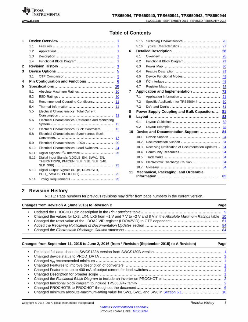
1.4 Functional Block Diagram
Figure 1-1. PMIC Functional Block Diagram
3
TPS65094, TPS650940, TPS650941, TPS650942, TPS650944www.ti.com SWCS133B –SEPTEMBER 2015–REVISED FEBRUARY 2017
Submit Documentation FeedbackProduct Folder Links: TPS65094
Revision HistoryCopyright © 2015–2017, Texas Instruments Incorporated
Table of Contents1 Device Overview ......................................... 1
1.1 Features .............................................. 11.2 Applications........................................... 11.3 Description............................................ 11.4 Functional Block Diagram ............................ 2
2 Revision History ......................................... 33 Device Options ........................................... 5
3.1 OTP Comparison ..................................... 54 Pin Configuration and Functions..................... 65 Specifications ........................................... 10
5.1 Absolute Maximum Ratings ......................... 105.2 ESD Ratings ........................................ 105.3 Recommended Operating Conditions............... 115.4 Thermal Information................................. 115.5 Electrical Characteristics: Total Current
Consumption ........................................ 115.6 Electrical Characteristics: Reference and Monitoring
System .............................................. 125.7 Electrical Characteristics: Buck Controllers ......... 135.8 Electrical Characteristics: Synchronous Buck
Converters........................................... 175.9 Electrical Characteristics: LDOs .................... 205.10 Electrical Characteristics: Load Switches ........... 245.11 Digital Signals: I2C Interface ........................ 255.12 Digital Input Signals (LDOLS_EN, SWA1_EN,
THERMTRIPB, PMICEN, SLP_S3B, SLP_S4B,SLP_S0B) ........................................... 25
5.13 Digital Output Signals (IRQB, RSMRSTB,PCH_PWROK, PROCHOT)......................... 25
5.14 Timing Requirements ............................... 25
5.15 Switching Characteristics ........................... 265.16 Typical Characteristics .............................. 27
6 Detailed Description ................................... 286.1 Overview ............................................ 286.2 Functional Block Diagram........................... 296.3 Power Map .......................................... 306.4 Feature Description ................................. 316.5 Device Functional Modes ........................... 486.6 I2C Interface ......................................... 486.7 Register Maps ....................................... 52
7 Application and Implementation .................... 717.1 Application Information .............................. 717.2 Specific Application for TPS650944 ................ 807.3 Do's and Don'ts ..................................... 81
8 Power Supply Coupling and Bulk Capacitors.... 819 Layout .................................................... 82
9.1 Layout Guidelines ................................... 829.2 Layout Example ..................................... 83
10 Device and Documentation Support ............... 8410.1 Device Support ..................................... 8410.2 Documentation Support ............................. 8410.3 Receiving Notification of Documentation Updates .. 8410.4 Community Resources .............................. 8410.5 Trademarks.......................................... 8410.6 Electrostatic Discharge Caution..................... 8410.7 Glossary ............................................. 84
11 Mechanical, Packaging, and OrderableInformation .............................................. 85
2 Revision HistoryNOTE: Page numbers for previous revisions may differ from page numbers in the current version.
Changes from Revision A (June 2016) to Revision B Page
• Updated the PROCHOT pin description in the Pin Functions table............................................................ 9• Changed the values for LX3, LX4, LX5 from –1 V and 7 V to –2 V and 8 V in the Absolute Maximum Ratings table 10• Changed the reset value of the LDOA2 VID register (LDOA2VID) to OTP dependent .................................... 61• Added the Receiving Notification of Documentation Updates section ....................................................... 84• Changed the Electrostatic Discharge Caution statement ...................................................................... 84
Changes from September 11, 2015 to June 2, 2016 (from * Revision (September 2015) to A Revision) Page
• Released full data sheet as SWCS133A version from SWCS130B version .................................................. 1• Changed device status to PROD_DATA .......................................................................................... 1• Changed VIN recommended minimum ............................................................................................. 1• Changed Features to improve description of converters ....................................................................... 1• Changed Features to up to 400 mA of output current for load switches ...................................................... 1• Changed Description for broader scope .......................................................................................... 1• Changed the Functional Block Diagram to include an inverter on PROCHOT pin........................................... 2• Changed functional block diagram to include TPS65094x family ............................................................. 2• Changed PROCHOTB to PROCHOT throughout the document ............................................................... 6• Changed minimum absolute-maximum-rating value for SW1, SW2, and SW6 in Section 5.1............................ 10
4
TPS65094, TPS650940, TPS650941, TPS650942, TPS650944SWCS133B –SEPTEMBER 2015–REVISED FEBRUARY 2017 www.ti.com
Submit Documentation FeedbackProduct Folder Links: TPS65094
Revision History Copyright © 2015–2017, Texas Instruments Incorporated
• Changed VSYS in Section 5.3, Recommended Operating Conditions ...................................................... 11• Deleted nominal value from PVINVTT in Section 5.3, Recommended Operating Conditions ........................... 11• Deleted (nu = symbol for efficiency) ............................................................................................. 13• Changed BUCK1 DC output voltage step size to show full range and be consistent in Section 5.7 .................... 13• Changed typo to match correct default of 1 V for ΔVOUT_TR in Section 5.7 ................................................. 13• Changed BUCK2 DC output voltage to show full range and be consistent in Section 5.7 ................................ 14• Changed set condition for BUCK6 for VOUT range in Section 5.7 to match BUCK1 and BUCK2 ........................ 15• Updated formatting and added new OTP information for BUCK6 in Section 5.7 ........................................... 15• Updated formatting for BUCK3 DC output voltage in Section 5.8 ............................................................ 17• Changed DC output voltage formatting for BUCK4 in Section 5.8 ........................................................... 18• Changed maximum IOUT value for BUCK4 in Section 5.8 to match device capabilities ................................... 18• Changed IOUT and ΔVOUT/ΔIOUT for VTT LDO in Section 5.9 for new OTPs ................................................. 23• Changed test conditions for VTT LDO overcurrent protection in Section 5.9 ............................................... 23• Changed Section 5.10 to show SWB1_2 RDSON is specified per output .................................................... 24• Changed fSW values in Section 5.15 to provide more values ................................................................. 26• Changed current to 1.9 A to match SoC requirements in Table 6-1 ......................................................... 28• Changed BUCK6, LDOA2, LDOA3 typical output voltage range to: OTP Dependent in Table 6-1 ...................... 28• Changed table note to include additional DDR types in Table 6-1 ........................................................... 28• Changed PMIC Functional Block Diagram to match specifications table ................................................... 29• Changed PROCHOTB to PROCHOT in the Apollo Lake Power Map ....................................................... 30• Changed current ratings in Apollo Lake Power Map ........................................................................... 30• Deleted SWBx PG from PG of PCH_PWROK in Table 6-2 ................................................................... 31• Changed BUCK1–2 to all BUCKs and LDOAs in Section 6.4.3.3 ............................................................ 36• Added Table 6-5 and Table 6-6 to Section 6.4.4.2 ............................................................................. 38• Added more DDR values to the table note in Table 6-7 ....................................................................... 39• Changed Section 6.4.5 to include LDOA1 and reset information ............................................................. 40• Changed Section 6.7 to include multiple DDRs ................................................................................. 40• Changed Figure 6-7 and Figure 6-8 to include alternate SWB1_2 Timing .................................................. 42• Changed SWB1_2 from: V3P3A to: V1P8U in Table 6-10 .................................................................... 42• Changed VDDQ voltage to OTP Dependent and SWBx to SWB1_2 in Table 6-11 ....................................... 44• Updated Figure 6-10 to include alternate SWB1_2 Timing .................................................................... 45• Changed Section 6.4.5.5 to include alternate SWB1_2 Timing ............................................................... 46• Changed Section 6.4.5.6 to include THERMTRIPB ........................................................................... 47• Added the TPS65094x family OTP values to Section 6.7 ..................................................................... 52• Replaced VID values with link to full VID table in Table 6-18 and Table 6-19 .............................................. 55• Updated naming of bits in the TEMPHOT register.............................................................................. 70
5
TPS65094, TPS650940, TPS650941, TPS650942, TPS650944www.ti.com SWCS133B –SEPTEMBER 2015–REVISED FEBRUARY 2017
Submit Documentation FeedbackProduct Folder Links: TPS65094
Device OptionsCopyright © 2015–2017, Texas Instruments Incorporated
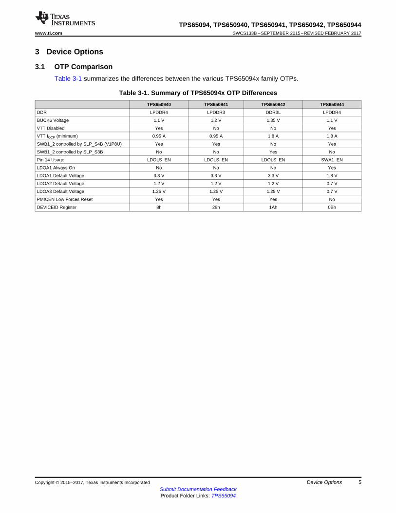
3 Device Options
3.1 OTP ComparisonTable 3-1 summarizes the differences between the various TPS65094x family OTPs.
Table 3-1. Summary of TPS65094x OTP DifferencesTPS650940 TPS650941 TPS650942 TPS650944
DDR LPDDR4 LPDDR3 DDR3L LPDDR4
BUCK6 Voltage 1.1 V 1.2 V 1.35 V 1.1 V
VTT Disabled Yes No No Yes
VTT IOCP (minimum) 0.95 A 0.95 A 1.8 A 1.8 A
SWB1_2 controlled by SLP_S4B (V1P8U) Yes Yes No Yes
SWB1_2 controlled by SLP_S3B No No Yes No
Pin 14 Usage LDOLS_EN LDOLS_EN LDOLS_EN SWA1_EN
LDOA1 Always On No No No Yes
LDOA1 Default Voltage 3.3 V 3.3 V 3.3 V 1.8 V
LDOA2 Default Voltage 1.2 V 1.2 V 1.2 V 0.7 V
LDOA3 Default Voltage 1.25 V 1.25 V 1.25 V 0.7 V
PMICEN Low Forces Reset Yes Yes Yes No
DEVICEID Register 8h 29h 1Ah 0Bh
1
2
3
4
5
6
7
8
9
10
11
12
13
14
15
16
1817
48
47
46
45
44
43
42
41
40
39
38
37
36
35
34
33
FBGND2
2019 2221 2423 2625 2827 3029 3231
6364 6162 5960 5758 5556 5354 5152 4950
FBVOUT2
DRVH2
SW2
BOOT2
PGNDSNS2
DRVL2
DRV5V_2_A1
LDOA1
LX3
PVIN3
FB3
PMICEN
LDOLS_EN orSWA1_EN
IRQB
RSMRSTB
VTTFB
VTT
PVINVTT
ILIM6
FBVOUT6
DRVH6
SW6
BOOT6
PGNDSNS6
DRVL6
DRV5V_1_6
DRVL1
PGNDSNS1
BOOT1
SW1
DRVH1
SW
B1
PV
INS
WB
1_B
2
SW
B2
LX5
PV
IN5
FB
5
FB
4
PV
IN4
LX4
FB
VO
UT
1
ILIM
1
SW
A1
PV
INS
WA
1
ILIM
2
SLP
_S4B
SLP
_S3B
SLP
_S0B
DA
TA
CLK
V5A
NA
LDO
5P0
VS
YS
LDO
3P3
VR
EF
AG
ND
LDO
A2
PV
INL
DO
A2_
A3
LDO
A3
TOP VIEWPGND/Thermal Pad
PR
OC
HO
T
GP
O
PC
H_P
WR
OK
TH
ER
MT
RIP
B
6
TPS65094, TPS650940, TPS650941, TPS650942, TPS650944SWCS133B –SEPTEMBER 2015–REVISED FEBRUARY 2017 www.ti.com
Submit Documentation FeedbackProduct Folder Links: TPS65094
Pin Configuration and Functions Copyright © 2015–2017, Texas Instruments Incorporated
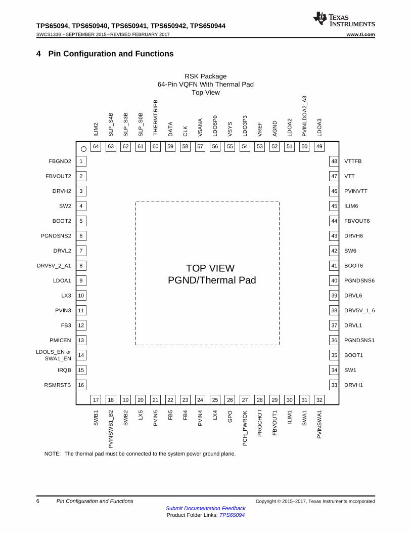
4 Pin Configuration and Functions
RSK Package64-Pin VQFN With Thermal Pad
Top View
NOTE: The thermal pad must be connected to the system power ground plane.
7
TPS65094, TPS650940, TPS650941, TPS650942, TPS650944www.ti.com SWCS133B –SEPTEMBER 2015–REVISED FEBRUARY 2017
Submit Documentation FeedbackProduct Folder Links: TPS65094
Pin Configuration and FunctionsCopyright © 2015–2017, Texas Instruments Incorporated
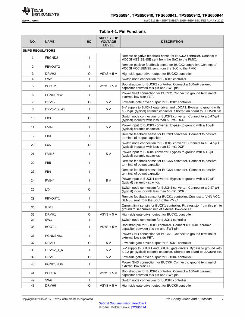
Table 4-1. Pin Functions
NO. NAME I/OSUPPLY, OP
VOLTAGELEVEL
DESCRIPTION
SMPS REGULATORS
1 FBGND2 I Remote negative feedback sense for BUCK2 controller. Connect toVCCGI VSS SENSE sent from the SoC to the PMIC.
2 FBVOUT2 I Remote positive feedback sense for BUCK2 controller. Connect toVCCGI VCC SENSE sent from the SoC to the PMIC.
3 DRVH2 O VSYS + 5 V High-side gate driver output for BUCK2 controller4 SW2 I Switch node connection for BUCK2 controller
5 BOOT2 I VSYS + 5 V Bootstrap pin for BUCK2 controller. Connect a 100-nF ceramiccapacitor between this pin and SW2 pin.
6 PGNDSNS2 I Power GND connection for BUCK2. Connect to ground terminal ofexternal low-side FET.
7 DRVL2 O 5 V Low-side gate driver output for BUCK2 controller
8 DRV5V_2_A1 I 5 V 5-V supply to BUCK2 gate driver and LDOA1. Bypass to ground witha 2.2-µF (typical) ceramic capacitor. Shorted on board to LDO5P0 pin.
10 LX3 O Switch node connection for BUCK3 converter. Connect to a 0.47-µH(typical) inductor with less than 50-mΩ DCR.
11 PVIN3 I 5 V Power input to BUCK3 converter. Bypass to ground with a 10-µF(typical) ceramic capacitor.
12 FB3 I Remote feedback sense for BUCK3 converter. Connect to positiveterminal of output capacitor.
20 LX5 O Switch node connection for BUCK5 converter. Connect to a 0.47-µH(typical) inductor with less than 50-mΩ DCR.
21 PVIN5 I 5 V Power input to BUCK5 converter. Bypass to ground with a 10-µF(typical) ceramic capacitor.
22 FB5 I Remote feedback sense for BUCK5 converter. Connect to positiveterminal of output capacitor.
23 FB4 I Remote feedback sense for BUCK4 converter. Connect to positiveterminal of output capacitor.
24 PVIN4 I 5 V Power input to BUCK4 converter. Bypass to ground with a 10-µF(typical) ceramic capacitor.
25 LX4 O Switch node connection for BUCK4 converter. Connect to a 0.47-µH(typical) inductor with less than 50-mΩ DCR.
29 FBVOUT1 I Remote feedback sense for BUCK1 controller. Connect to VNN VCCSENSE sent from the SoC to the PMIC.
30 ILIM1 I Current limit set pin for BUCK1 controller. Fit a resistor from this pin toground to set current limit of external low-side FET.
33 DRVH1 O VSYS + 5 V High-side gate driver output for BUCK1 controller34 SW1 I Switch node connection for BUCK1 controller
35 BOOT1 I VSYS + 5 V Bootstrap pin for BUCK1 controller. Connect a 100-nF ceramiccapacitor between this pin and SW1 pin.
36 PGNDSNS1 I Power GND connection for BUCK1. Connect to ground terminal ofexternal low-side FET.
37 DRVL1 O 5 V Low-side gate driver output for BUCK1 controller
38 DRV5V_1_6 I 5 V 5-V supply to BUCK1 and BUCK6 gate drivers. Bypass to ground witha 2.2-µF (typical) ceramic capacitor. Shorted on board to LDO5P0 pin.
39 DRVL6 O 5 V Low-side gate driver output for BUCK6 controller
40 PGNDSNS6 I Power GND connection for BUCK6. Connect to ground terminal ofexternal low-side FET.
41 BOOT6 I VSYS + 5 V Bootstrap pin for BUCK6 controller. Connect a 100-nF ceramiccapacitor between this pin and SW6 pin.
42 SW6 I Switch node connection for BUCK6 controller43 DRVH6 O VSYS + 5 V High-side gate driver output for BUCK6 controller
8
TPS65094, TPS650940, TPS650941, TPS650942, TPS650944SWCS133B –SEPTEMBER 2015–REVISED FEBRUARY 2017 www.ti.com
Submit Documentation FeedbackProduct Folder Links: TPS65094
Pin Configuration and Functions Copyright © 2015–2017, Texas Instruments Incorporated
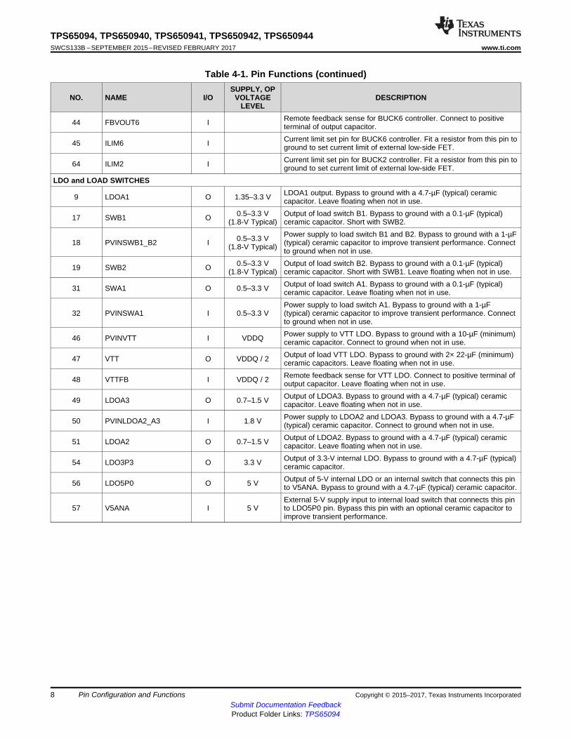
Table 4-1. Pin Functions (continued)
NO. NAME I/OSUPPLY, OP
VOLTAGELEVEL
DESCRIPTION
44 FBVOUT6 I Remote feedback sense for BUCK6 controller. Connect to positiveterminal of output capacitor.
45 ILIM6 I Current limit set pin for BUCK6 controller. Fit a resistor from this pin toground to set current limit of external low-side FET.
64 ILIM2 I Current limit set pin for BUCK2 controller. Fit a resistor from this pin toground to set current limit of external low-side FET.
LDO and LOAD SWITCHES
9 LDOA1 O 1.35–3.3 V LDOA1 output. Bypass to ground with a 4.7-µF (typical) ceramiccapacitor. Leave floating when not in use.
17 SWB1 O 0.5–3.3 V(1.8-V Typical)
Output of load switch B1. Bypass to ground with a 0.1-µF (typical)ceramic capacitor. Short with SWB2.
18 PVINSWB1_B2 I 0.5–3.3 V(1.8-V Typical)
Power supply to load switch B1 and B2. Bypass to ground with a 1-µF(typical) ceramic capacitor to improve transient performance. Connectto ground when not in use.
19 SWB2 O 0.5–3.3 V(1.8-V Typical)
Output of load switch B2. Bypass to ground with a 0.1-µF (typical)ceramic capacitor. Short with SWB1. Leave floating when not in use.
31 SWA1 O 0.5–3.3 V Output of load switch A1. Bypass to ground with a 0.1-µF (typical)ceramic capacitor. Leave floating when not in use.
32 PVINSWA1 I 0.5–3.3 VPower supply to load switch A1. Bypass to ground with a 1-µF(typical) ceramic capacitor to improve transient performance. Connectto ground when not in use.
46 PVINVTT I VDDQ Power supply to VTT LDO. Bypass to ground with a 10-µF (minimum)ceramic capacitor. Connect to ground when not in use.
47 VTT O VDDQ / 2 Output of load VTT LDO. Bypass to ground with 2× 22-µF (minimum)ceramic capacitors. Leave floating when not in use.
48 VTTFB I VDDQ / 2 Remote feedback sense for VTT LDO. Connect to positive terminal ofoutput capacitor. Leave floating when not in use.
49 LDOA3 O 0.7–1.5 V Output of LDOA3. Bypass to ground with a 4.7-µF (typical) ceramiccapacitor. Leave floating when not in use.
50 PVINLDOA2_A3 I 1.8 V Power supply to LDOA2 and LDOA3. Bypass to ground with a 4.7-µF(typical) ceramic capacitor. Connect to ground when not in use.
51 LDOA2 O 0.7–1.5 V Output of LDOA2. Bypass to ground with a 4.7-µF (typical) ceramiccapacitor. Leave floating when not in use.
54 LDO3P3 O 3.3 V Output of 3.3-V internal LDO. Bypass to ground with a 4.7-µF (typical)ceramic capacitor.
56 LDO5P0 O 5 V Output of 5-V internal LDO or an internal switch that connects this pinto V5ANA. Bypass to ground with a 4.7-µF (typical) ceramic capacitor.
57 V5ANA I 5 VExternal 5-V supply input to internal load switch that connects this pinto LDO5P0 pin. Bypass this pin with an optional ceramic capacitor toimprove transient performance.
9
TPS65094, TPS650940, TPS650941, TPS650942, TPS650944www.ti.com SWCS133B –SEPTEMBER 2015–REVISED FEBRUARY 2017
Submit Documentation FeedbackProduct Folder Links: TPS65094
Pin Configuration and FunctionsCopyright © 2015–2017, Texas Instruments Incorporated
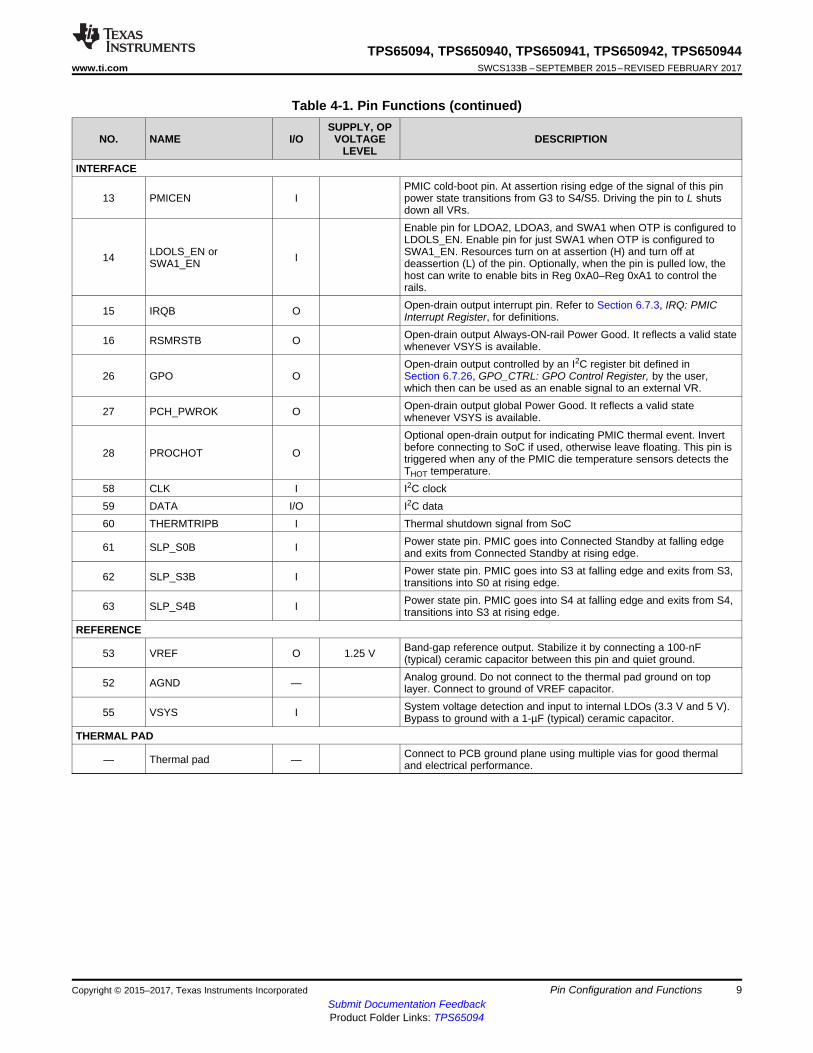
Table 4-1. Pin Functions (continued)
NO. NAME I/OSUPPLY, OP
VOLTAGELEVEL
DESCRIPTION
INTERFACE
13 PMICEN IPMIC cold-boot pin. At assertion rising edge of the signal of this pinpower state transitions from G3 to S4/S5. Driving the pin to L shutsdown all VRs.
14 LDOLS_EN orSWA1_EN I
Enable pin for LDOA2, LDOA3, and SWA1 when OTP is configured toLDOLS_EN. Enable pin for just SWA1 when OTP is configured toSWA1_EN. Resources turn on at assertion (H) and turn off atdeassertion (L) of the pin. Optionally, when the pin is pulled low, thehost can write to enable bits in Reg 0xA0–Reg 0xA1 to control therails.
15 IRQB O Open-drain output interrupt pin. Refer to Section 6.7.3, IRQ: PMICInterrupt Register, for definitions.
16 RSMRSTB O Open-drain output Always-ON-rail Power Good. It reflects a valid statewhenever VSYS is available.
26 GPO OOpen-drain output controlled by an I2C register bit defined inSection 6.7.26, GPO_CTRL: GPO Control Register, by the user,which then can be used as an enable signal to an external VR.
27 PCH_PWROK O Open-drain output global Power Good. It reflects a valid statewhenever VSYS is available.
28 PROCHOT O
Optional open-drain output for indicating PMIC thermal event. Invertbefore connecting to SoC if used, otherwise leave floating. This pin istriggered when any of the PMIC die temperature sensors detects theTHOT temperature.
58 CLK I I2C clock59 DATA I/O I2C data60 THERMTRIPB I Thermal shutdown signal from SoC
61 SLP_S0B I Power state pin. PMIC goes into Connected Standby at falling edgeand exits from Connected Standby at rising edge.
62 SLP_S3B I Power state pin. PMIC goes into S3 at falling edge and exits from S3,transitions into S0 at rising edge.
63 SLP_S4B I Power state pin. PMIC goes into S4 at falling edge and exits from S4,transitions into S3 at rising edge.
REFERENCE
53 VREF O 1.25 V Band-gap reference output. Stabilize it by connecting a 100-nF(typical) ceramic capacitor between this pin and quiet ground.
52 AGND — Analog ground. Do not connect to the thermal pad ground on toplayer. Connect to ground of VREF capacitor.
55 VSYS I System voltage detection and input to internal LDOs (3.3 V and 5 V).Bypass to ground with a 1-µF (typical) ceramic capacitor.
THERMAL PAD
— Thermal pad — Connect to PCB ground plane using multiple vias for good thermaland electrical performance.
10
TPS65094, TPS650940, TPS650941, TPS650942, TPS650944SWCS133B –SEPTEMBER 2015–REVISED FEBRUARY 2017 www.ti.com
Submit Documentation FeedbackProduct Folder Links: TPS65094
Specifications Copyright © 2015–2017, Texas Instruments Incorporated
(1) Stresses beyond those listed under Absolute Maximum Ratings may cause permanent damage to the device. These are stress ratingsonly, and functional operation of the device at these or any other conditions beyond those indicated under Recommended OperatingConditions is not implied. Exposure to absolute-maximum-rated conditions for extended periods may affect device reliability.
(2) Transient for less than 5 ns.(3) Transient for less than 20 ns.
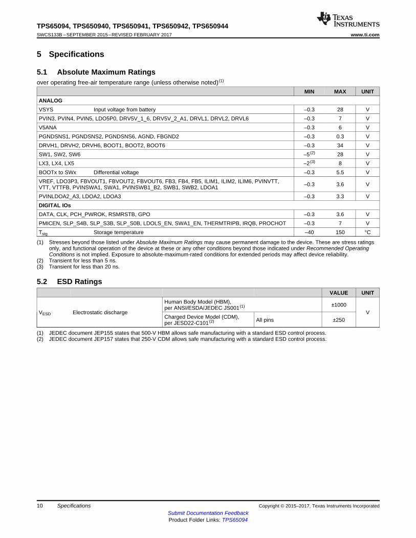
5 Specifications
5.1 Absolute Maximum Ratingsover operating free-air temperature range (unless otherwise noted) (1)
MIN MAX UNITANALOGVSYS Input voltage from battery –0.3 28 VPVIN3, PVIN4, PVIN5, LDO5P0, DRV5V_1_6, DRV5V_2_A1, DRVL1, DRVL2, DRVL6 –0.3 7 VV5ANA –0.3 6 VPGNDSNS1, PGNDSNS2, PGNDSNS6, AGND, FBGND2 –0.3 0.3 VDRVH1, DRVH2, DRVH6, BOOT1, BOOT2, BOOT6 –0.3 34 VSW1, SW2, SW6 –5 (2) 28 VLX3, LX4, LX5 –2 (3) 8 VBOOTx to SWx Differential voltage –0.3 5.5 VVREF, LDO3P3, FBVOUT1, FBVOUT2, FBVOUT6, FB3, FB4, FB5, ILIM1, ILIM2, ILIM6, PVINVTT,VTT, VTTFB, PVINSWA1, SWA1, PVINSWB1_B2, SWB1, SWB2, LDOA1 –0.3 3.6 V
PVINLDOA2_A3, LDOA2, LDOA3 –0.3 3.3 VDIGITAL IOsDATA, CLK, PCH_PWROK, RSMRSTB, GPO –0.3 3.6 VPMICEN, SLP_S4B, SLP_S3B, SLP_S0B, LDOLS_EN, SWA1_EN, THERMTRIPB, IRQB, PROCHOT –0.3 7 VTstg Storage temperature –40 150 °C
(1) JEDEC document JEP155 states that 500-V HBM allows safe manufacturing with a standard ESD control process.(2) JEDEC document JEP157 states that 250-V CDM allows safe manufacturing with a standard ESD control process.
5.2 ESD RatingsVALUE UNIT
VESD Electrostatic discharge
Human Body Model (HBM),per ANSI/ESDA/JEDEC JS001 (1) ±1000
VCharged Device Model (CDM),per JESD22-C101 (2) All pins ±250
11
TPS65094, TPS650940, TPS650941, TPS650942, TPS650944www.ti.com SWCS133B –SEPTEMBER 2015–REVISED FEBRUARY 2017
Submit Documentation FeedbackProduct Folder Links: TPS65094
SpecificationsCopyright © 2015–2017, Texas Instruments Incorporated
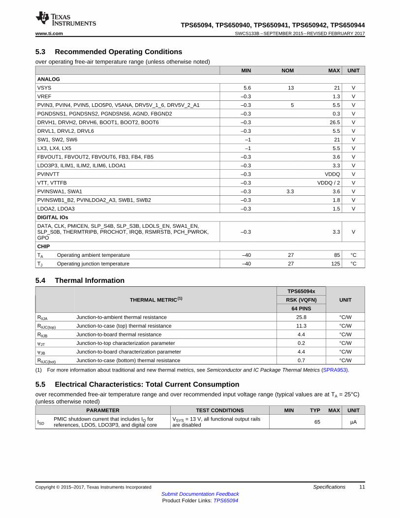
5.3 Recommended Operating Conditionsover operating free-air temperature range (unless otherwise noted)
MIN NOM MAX UNITANALOGVSYS 5.6 13 21 VVREF –0.3 1.3 VPVIN3, PVIN4, PVIN5, LDO5P0, V5ANA, DRV5V_1_6, DRV5V_2_A1 –0.3 5 5.5 VPGNDSNS1, PGNDSNS2, PGNDSNS6, AGND, FBGND2 –0.3 0.3 VDRVH1, DRVH2, DRVH6, BOOT1, BOOT2, BOOT6 –0.3 26.5 VDRVL1, DRVL2, DRVL6 –0.3 5.5 VSW1, SW2, SW6 –1 21 VLX3, LX4, LX5 –1 5.5 VFBVOUT1, FBVOUT2, FBVOUT6, FB3, FB4, FB5 –0.3 3.6 VLDO3P3, ILIM1, ILIM2, ILIM6, LDOA1 –0.3 3.3 VPVINVTT –0.3 VDDQ VVTT, VTTFB –0.3 VDDQ / 2 VPVINSWA1, SWA1 –0.3 3.3 3.6 VPVINSWB1_B2, PVINLDOA2_A3, SWB1, SWB2 –0.3 1.8 VLDOA2, LDOA3 –0.3 1.5 VDIGITAL IOsDATA, CLK, PMICEN, SLP_S4B, SLP_S3B, LDOLS_EN, SWA1_EN,SLP_S0B, THERMTRIPB, PROCHOT, IRQB, RSMRSTB, PCH_PWROK,GPO
–0.3 3.3 V
CHIPTA Operating ambient temperature –40 27 85 °CTJ Operating junction temperature –40 27 125 °C
(1) For more information about traditional and new thermal metrics, see Semiconductor and IC Package Thermal Metrics (SPRA953).
5.4 Thermal Information
THERMAL METRIC (1)TPS65094x
UNITRSK (VQFN)64 PINS
RθJA Junction-to-ambient thermal resistance 25.8 °C/WRθJC(top) Junction-to-case (top) thermal resistance 11.3 °C/WRθJB Junction-to-board thermal resistance 4.4 °C/WψJT Junction-to-top characterization parameter 0.2 °C/WψJB Junction-to-board characterization parameter 4.4 °C/WRθJC(bot) Junction-to-case (bottom) thermal resistance 0.7 °C/W
5.5 Electrical Characteristics: Total Current Consumptionover recommended free-air temperature range and over recommended input voltage range (typical values are at TA = 25°C)(unless otherwise noted)
PARAMETER TEST CONDITIONS MIN TYP MAX UNIT
ISDPMIC shutdown current that includes IQ forreferences, LDO5, LDO3P3, and digital core
VSYS = 13 V, all functional output railsare disabled 65 µA
12
TPS65094, TPS650940, TPS650941, TPS650942, TPS650944SWCS133B –SEPTEMBER 2015–REVISED FEBRUARY 2017 www.ti.com
Submit Documentation FeedbackProduct Folder Links: TPS65094
Specifications Copyright © 2015–2017, Texas Instruments Incorporated
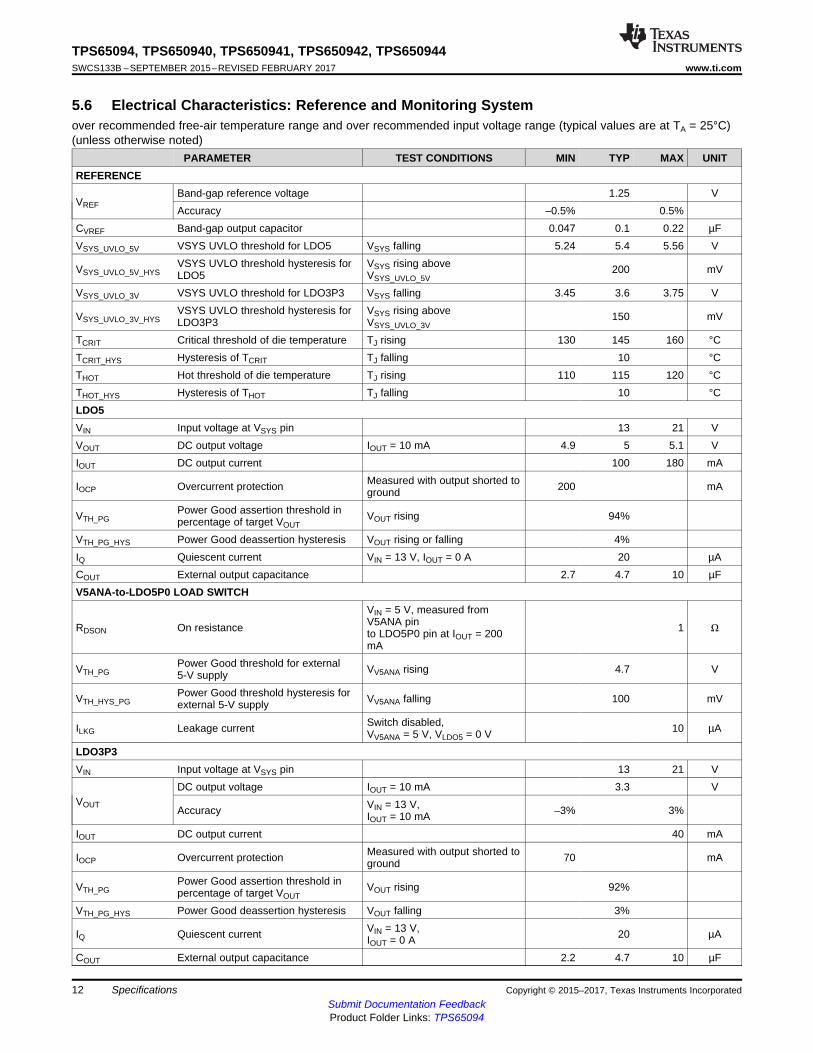
5.6 Electrical Characteristics: Reference and Monitoring Systemover recommended free-air temperature range and over recommended input voltage range (typical values are at TA = 25°C)(unless otherwise noted)
PARAMETER TEST CONDITIONS MIN TYP MAX UNITREFERENCE
VREFBand-gap reference voltage 1.25 VAccuracy –0.5% 0.5%
CVREF Band-gap output capacitor 0.047 0.1 0.22 µFVSYS_UVLO_5V VSYS UVLO threshold for LDO5 VSYS falling 5.24 5.4 5.56 V
VSYS_UVLO_5V_HYSVSYS UVLO threshold hysteresis forLDO5
VSYS rising aboveVSYS_UVLO_5V
200 mV
VSYS_UVLO_3V VSYS UVLO threshold for LDO3P3 VSYS falling 3.45 3.6 3.75 V
VSYS_UVLO_3V_HYSVSYS UVLO threshold hysteresis forLDO3P3
VSYS rising aboveVSYS_UVLO_3V
150 mV
TCRIT Critical threshold of die temperature TJ rising 130 145 160 °CTCRIT_HYS Hysteresis of TCRIT TJ falling 10 °CTHOT Hot threshold of die temperature TJ rising 110 115 120 °CTHOT_HYS Hysteresis of THOT TJ falling 10 °CLDO5VIN Input voltage at VSYS pin 13 21 VVOUT DC output voltage IOUT = 10 mA 4.9 5 5.1 VIOUT DC output current 100 180 mA
IOCP Overcurrent protection Measured with output shorted toground 200 mA
VTH_PGPower Good assertion threshold inpercentage of target VOUT
VOUT rising 94%
VTH_PG_HYS Power Good deassertion hysteresis VOUT rising or falling 4%IQ Quiescent current VIN = 13 V, IOUT = 0 A 20 µACOUT External output capacitance 2.7 4.7 10 µFV5ANA-to-LDO5P0 LOAD SWITCH
RDSON On resistance
VIN = 5 V, measured fromV5ANA pinto LDO5P0 pin at IOUT = 200mA
1 Ω
VTH_PGPower Good threshold for external5-V supply VV5ANA rising 4.7 V
VTH_HYS_PGPower Good threshold hysteresis forexternal 5-V supply VV5ANA falling 100 mV
ILKG Leakage current Switch disabled,VV5ANA = 5 V, VLDO5 = 0 V 10 µA
LDO3P3VIN Input voltage at VSYS pin 13 21 V
VOUT
DC output voltage IOUT = 10 mA 3.3 V
Accuracy VIN = 13 V,IOUT = 10 mA –3% 3%
IOUT DC output current 40 mA
IOCP Overcurrent protection Measured with output shorted toground 70 mA
VTH_PGPower Good assertion threshold inpercentage of target VOUT
VOUT rising 92%
VTH_PG_HYS Power Good deassertion hysteresis VOUT falling 3%
IQ Quiescent current VIN = 13 V,IOUT = 0 A 20 µA
COUT External output capacitance 2.2 4.7 10 µF
13
TPS65094, TPS650940, TPS650941, TPS650942, TPS650944www.ti.com SWCS133B –SEPTEMBER 2015–REVISED FEBRUARY 2017
Submit Documentation FeedbackProduct Folder Links: TPS65094
SpecificationsCopyright © 2015–2017, Texas Instruments Incorporated
(1) Frequency of transient load current ranges from 0 to 1 MHz with duty cycle of 50%. For cases where duty cycle and frequency arelimited by tr and tf, the highest frequency is set by 1 / (tr + tf), where tr is rise time (0% to 100%) and tf is fall time (100% to 0%).
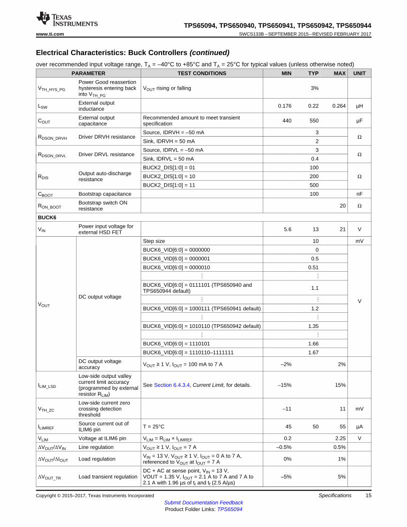
5.7 Electrical Characteristics: Buck Controllersover recommended input voltage range, TA = –40°C to +85°C and TA = 25°C for typical values (unless otherwise noted)
PARAMETER TEST CONDITIONS MIN TYP MAX UNITBUCK1
VINPower input voltage forexternal HSD FET 5.6 13 21 V
VOUT
DC output voltage
Step size 10 mVBUCK1_VID[6:0] = 0000000 0
V
BUCK1_VID[6:0] = 0000001 0.5BUCK1_VID[6:0] = 0000010 0.51
⋮ ⋮BUCK1_VID[6:0] = 0110011 (default) 1.00
⋮ ⋮BUCK1_VID[6:0] = 1110101 1.66BUCK1_VID[6:0] = 1110110–1111111 1.67
DC output voltageaccuracy
VOUT ≥ 1 V, IOUT = 100 mA to 5 A –2% 2%VOUT = 0.75 V, IOUT = 100 mA to 2.1 A –2.5% 2.5%VOUT ≤ 0.6 V, IOUT = 10 mA –3.5% 3.5%
Total output voltageaccuracy (DC + ripple) inDCM
IOUT = 10 mA, VOUT ≤ 0.785 V, VSYS = 13 V –20 40mV
IOUT = 10 mA, VOUT ≤ 0.785 V, VSYS = 21 V –20 55
SR(VOUT) Output DVS slew rate 2.5 3.125 mV/µs
ILIM_LSD
Low-side output valleycurrent limit accuracy(programmed by externalresistor RLIM)
See Section 6.4.3.4, Current Limit, for details. –15% 15%
VTH_ZC
Low-side current zerocrossing detectionthreshold
–11 11 mV
ILIMREFSource current out ofILIM1 pin T = 25°C 45 50 55 µA
VLIM Voltage at ILIM1 pin VLIM = RLIM × ILIMREF 0.2 2.25 VΔVOUT/ΔVIN Line regulation VOUT ≥ 1 V, IOUT = 5 A –0.5% 0.5%
ΔVOUT/ΔIOUT Load regulationVIN = 13 V, VOUT ≥ 1 V,IOUT = 0 A to 5 A,referenced to VOUT at IOUT = 5 A
0% 1%
ΔVOUT_TR(1) Load transient regulation
DC + AC at sense point, VIN = 13 V,VOUT = 1.00 V,IOUT = 1.5 A to 5 A and 5 A to 1.5 A with 1 µs oftr and tf –50 50 mVDC + AC at sense point, VIN = 13 V,VOUT = 0.75 V,IOUT = 0.3 A to 1.5 A and 1.5 A to 0.3 A with 1 µsof tr and tf
VTH_PG
Power Good deassertionthreshold in percentageof target VOUT
VOUT rising 108%
VOUT falling 92%
VTH_HYS_PG
Power Good reassertionhysteresis entering backinto VTH_PG
VOUT rising or falling 3%
COUTExternal outputcapacitance
Recommended amount to meet transientspecification 180 220 µF
LSWExternal outputinductance 0.376 0.47 0.564 µH
14
TPS65094, TPS650940, TPS650941, TPS650942, TPS650944SWCS133B –SEPTEMBER 2015–REVISED FEBRUARY 2017 www.ti.com
Submit Documentation FeedbackProduct Folder Links: TPS65094
Specifications Copyright © 2015–2017, Texas Instruments Incorporated
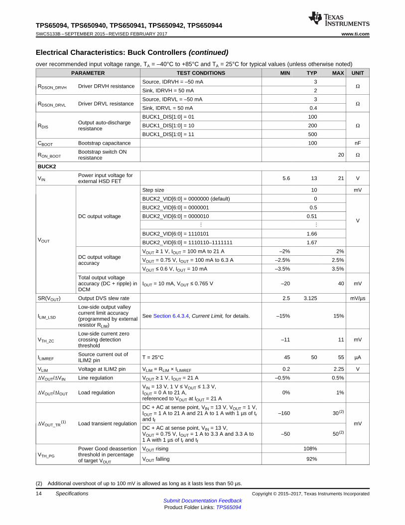
Electrical Characteristics: Buck Controllers (continued)over recommended input voltage range, TA = –40°C to +85°C and TA = 25°C for typical values (unless otherwise noted)
PARAMETER TEST CONDITIONS MIN TYP MAX UNIT
(2) Additional overshoot of up to 100 mV is allowed as long as it lasts less than 50 µs.
RDSON_DRVH Driver DRVH resistanceSource, IDRVH = –50 mA 3
ΩSink, IDRVH = 50 mA 2
RDSON_DRVL Driver DRVL resistanceSource, IDRVL = –50 mA 3
ΩSink, IDRVL = 50 mA 0.4
RDISOutput auto-dischargeresistance
BUCK1_DIS[1:0] = 01 100ΩBUCK1_DIS[1:0] = 10 200
BUCK1_DIS[1:0] = 11 500CBOOT Bootstrap capacitance 100 nF
RON_BOOTBootstrap switch ONresistance 20 Ω
BUCK2
VINPower input voltage forexternal HSD FET 5.6 13 21 V
VOUT
DC output voltage
Step size 10 mVBUCK2_VID[6:0] = 0000000 (default) 0
V
BUCK2_VID[6:0] = 0000001 0.5BUCK2_VID[6:0] = 0000010 0.51
⋮ ⋮BUCK2_VID[6:0] = 1110101 1.66BUCK2_VID[6:0] = 1110110–1111111 1.67
DC output voltageaccuracy
VOUT ≥ 1 V, IOUT = 100 mA to 21 A –2% 2%VOUT = 0.75 V, IOUT = 100 mA to 6.3 A –2.5% 2.5%VOUT ≤ 0.6 V, IOUT = 10 mA –3.5% 3.5%
Total output voltageaccuracy (DC + ripple) inDCM
IOUT = 10 mA, VOUT ≤ 0.765 V –20 40 mV
SR(VOUT) Output DVS slew rate 2.5 3.125 mV/µs
ILIM_LSD
Low-side output valleycurrent limit accuracy(programmed by externalresistor RLIM)
See Section 6.4.3.4, Current Limit, for details. –15% 15%
VTH_ZC
Low-side current zerocrossing detectionthreshold
–11 11 mV
ILIMREFSource current out ofILIM2 pin T = 25°C 45 50 55 µA
VLIM Voltage at ILIM2 pin VLIM = RLIM × ILIMREF 0.2 2.25 VΔVOUT/ΔVIN Line regulation VOUT ≥ 1 V, IOUT = 21 A –0.5% 0.5%
ΔVOUT/ΔIOUT Load regulationVIN = 13 V, 1 V ≤ VOUT ≤ 1.3 V,IOUT = 0 A to 21 A,referenced to VOUT at IOUT = 21 A
0% 1%
ΔVOUT_TR(1) Load transient regulation
DC + AC at sense point, VIN = 13 V, VOUT = 1 V,IOUT = 1 A to 21 A and 21 A to 1 A with 1 µs of trand tf
–160 30 (2)
mVDC + AC at sense point, VIN = 13 V,VOUT = 0.75 V, IOUT = 1 A to 3.3 A and 3.3 A to1 A with 1 µs of tr and tf
–50 50 (2)
VTH_PG
Power Good deassertionthreshold in percentageof target VOUT
VOUT rising 108%
VOUT falling 92%
15
TPS65094, TPS650940, TPS650941, TPS650942, TPS650944www.ti.com SWCS133B –SEPTEMBER 2015–REVISED FEBRUARY 2017
Submit Documentation FeedbackProduct Folder Links: TPS65094
SpecificationsCopyright © 2015–2017, Texas Instruments Incorporated
Electrical Characteristics: Buck Controllers (continued)over recommended input voltage range, TA = –40°C to +85°C and TA = 25°C for typical values (unless otherwise noted)
PARAMETER TEST CONDITIONS MIN TYP MAX UNIT
VTH_HYS_PG
Power Good reassertionhysteresis entering backinto VTH_PG
VOUT rising or falling 3%
LSWExternal outputinductance 0.176 0.22 0.264 µH
COUTExternal outputcapacitance
Recommended amount to meet transientspecification 440 550 µF
RDSON_DRVH Driver DRVH resistanceSource, IDRVH = –50 mA 3
ΩSink, IDRVH = 50 mA 2
RDSON_DRVL Driver DRVL resistanceSource, IDRVL = –50 mA 3
ΩSink, IDRVL = 50 mA 0.4
RDISOutput auto-dischargeresistance
BUCK2_DIS[1:0] = 01 100ΩBUCK2_DIS[1:0] = 10 200
BUCK2_DIS[1:0] = 11 500CBOOT Bootstrap capacitance 100 nF
RON_BOOTBootstrap switch ONresistance 20 Ω
BUCK6
VINPower input voltage forexternal HSD FET 5.6 13 21 V
VOUT
DC output voltage
Step size 10 mVBUCK6_VID[6:0] = 0000000 0
V
BUCK6_VID[6:0] = 0000001 0.5BUCK6_VID[6:0] = 0000010 0.51
⋮ ⋮BUCK6_VID[6:0] = 0111101 (TPS650940 andTPS650944 default) 1.1
⋮ ⋮BUCK6_VID[6:0] = 1000111 (TPS650941 default) 1.2
⋮ ⋮BUCK6_VID[6:0] = 1010110 (TPS650942 default) 1.35
⋮ ⋮BUCK6_VID[6:0] = 1110101 1.66BUCK6_VID[6:0] = 1110110–1111111 1.67
DC output voltageaccuracy VOUT ≥ 1 V, IOUT = 100 mA to 7 A –2% 2%
ILIM_LSD
Low-side output valleycurrent limit accuracy(programmed by externalresistor RLIM)
See Section 6.4.3.4, Current Limit, for details. –15% 15%
VTH_ZC
Low-side current zerocrossing detectionthreshold
–11 11 mV
ILIMREFSource current out ofILIM6 pin T = 25°C 45 50 55 µA
VLIM Voltage at ILIM6 pin VLIM = RLIM × ILIMREF 0.2 2.25 VΔVOUT/ΔVIN Line regulation VOUT ≥ 1 V, IOUT = 7 A –0.5% 0.5%
ΔVOUT/ΔIOUT Load regulation VIN = 13 V, VOUT ≥ 1 V, IOUT = 0 A to 7 A,referenced to VOUT at IOUT = 7 A 0% 1%
ΔVOUT_TR Load transient regulationDC + AC at sense point, VIN = 13 V,VOUT = 1.35 V, IOUT = 2.1 A to 7 A and 7 A to2.1 A with 1.96 µs of tr and tf (2.5 A/µs)
–5% 5%
16
TPS65094, TPS650940, TPS650941, TPS650942, TPS650944SWCS133B –SEPTEMBER 2015–REVISED FEBRUARY 2017 www.ti.com
Submit Documentation FeedbackProduct Folder Links: TPS65094
Specifications Copyright © 2015–2017, Texas Instruments Incorporated
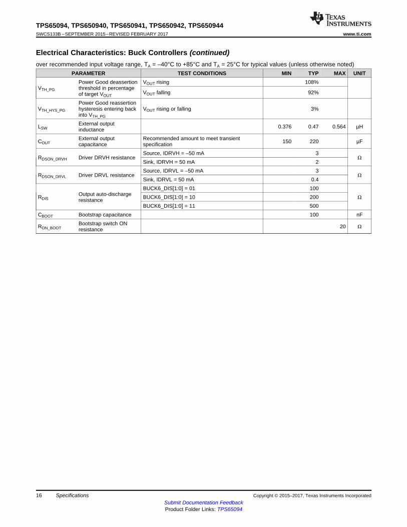
Electrical Characteristics: Buck Controllers (continued)over recommended input voltage range, TA = –40°C to +85°C and TA = 25°C for typical values (unless otherwise noted)
PARAMETER TEST CONDITIONS MIN TYP MAX UNIT
VTH_PG
Power Good deassertionthreshold in percentageof target VOUT
VOUT rising 108%
VOUT falling 92%
VTH_HYS_PG
Power Good reassertionhysteresis entering backinto VTH_PG
VOUT rising or falling 3%
LSWExternal outputinductance 0.376 0.47 0.564 µH
COUTExternal outputcapacitance
Recommended amount to meet transientspecification 150 220 µF
RDSON_DRVH Driver DRVH resistanceSource, IDRVH = –50 mA 3
ΩSink, IDRVH = 50 mA 2
RDSON_DRVL Driver DRVL resistanceSource, IDRVL = –50 mA 3
ΩSink, IDRVL = 50 mA 0.4
RDISOutput auto-dischargeresistance
BUCK6_DIS[1:0] = 01 100ΩBUCK6_DIS[1:0] = 10 200
BUCK6_DIS[1:0] = 11 500CBOOT Bootstrap capacitance 100 nF
RON_BOOTBootstrap switch ONresistance 20 Ω
17
TPS65094, TPS650940, TPS650941, TPS650942, TPS650944www.ti.com SWCS133B –SEPTEMBER 2015–REVISED FEBRUARY 2017
Submit Documentation FeedbackProduct Folder Links: TPS65094
SpecificationsCopyright © 2015–2017, Texas Instruments Incorporated
(1) Frequency of transient load current ranges from 0 to 1 MHz with duty cycle of 50%. For cases where duty cycle and frequency arelimited by tr and tf, the highest frequency is set by 1 / (tr + tf), where tr is rise time (0% to 100%) and tf is fall time (100% to 0%).
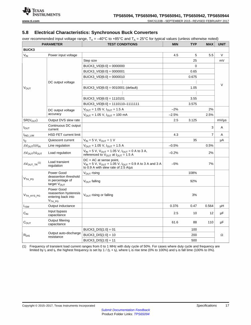
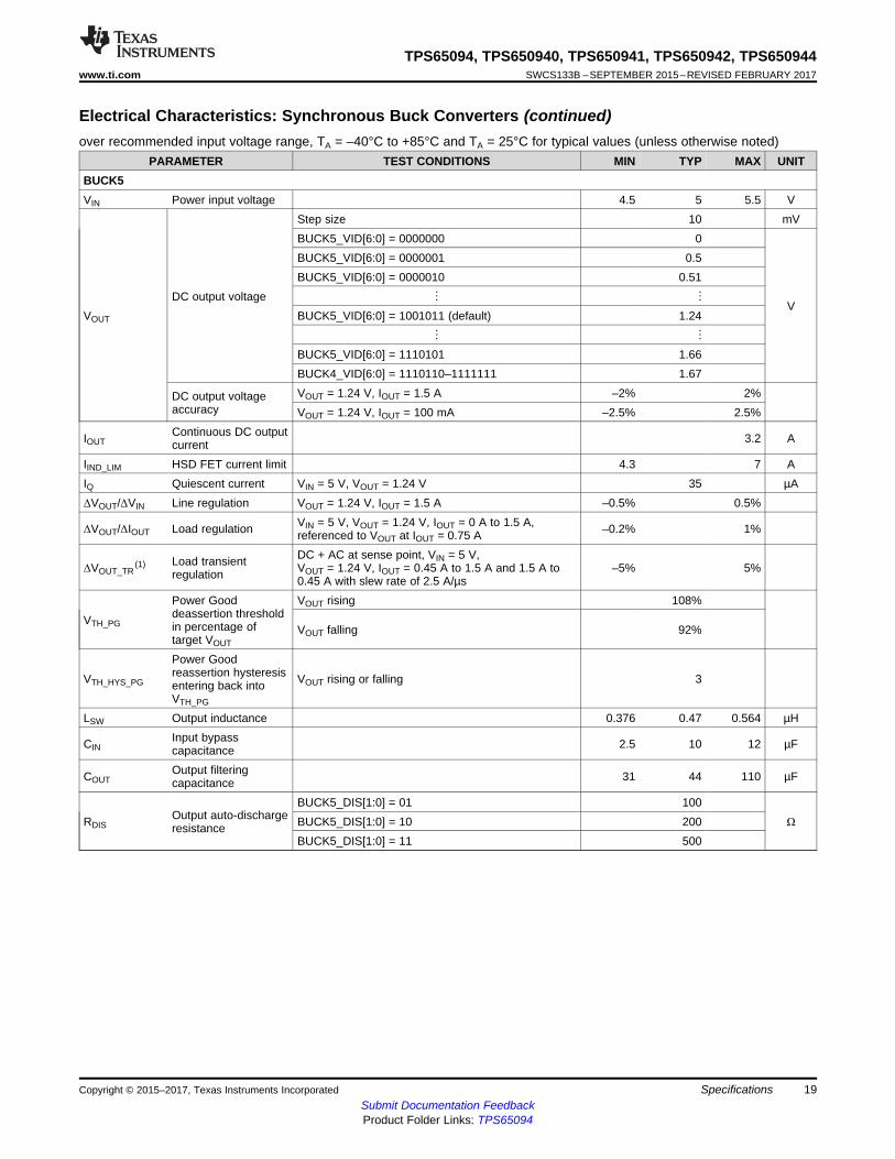
5.8 Electrical Characteristics: Synchronous Buck Convertersover recommended input voltage range, TA = –40°C to +85°C and TA = 25°C for typical values (unless otherwise noted)
PARAMETER TEST CONDITIONS MIN TYP MAX UNITBUCK3VIN Power input voltage 4.5 5 5.5 V
VOUT
DC output voltage
Step size 25 mVBUCK3_VID[6:0] = 0000000 0
V
BUCK3_VID[6:0] = 0000001 0.65BUCK3_VID[6:0] = 0000010 0.675
⋮ ⋮BUCK3_VID[6:0] = 0010001 (default) 1.05
⋮ ⋮BUCK3_VID[6:0] = 1110101 3.55BUCK3_VID[6:0] = 1110110–1111111 3.575
DC output voltageaccuracy
VOUT = 1.05 V, IOUT = 1.5 A –2% 2%VOUT = 1.05 V, IOUT = 100 mA –2.5% 2.5%
SR(VOUT) Output DVS slew rate 2.5 3.125 mV/µs
IOUTContinuous DC outputcurrent 3 A
IIND_LIM HSD FET current limit 4.3 7 AIQ Quiescent current VIN = 5 V, VOUT = 1 V 35 µAΔVOUT/ΔVIN Line regulation VOUT = 1.05 V, IOUT = 1.5 A –0.5% 0.5%
ΔVOUT/ΔIOUT Load regulation VIN = 5 V, VOUT = 1.05 V, IOUT = 0 A to 3 A,referenced to VOUT at IOUT = 1.5 A –0.2% 2%
ΔVOUT_TR(1) Load transient
regulation
DC + AC at sense point,VIN = 5 V, VOUT = 1.05 V, IOUT = 0.9 A to 3 A and 3 Ato 0.9 A with slew rate of 2.5 A/µs
–5% 7%
VTH_PG
Power Gooddeassertion thresholdin percentage oftarget VOUT
VOUT rising 108%
VOUT falling 92%
VTH_HYS_PG
Power Goodreassertion hysteresisentering back intoVTH_PG
VOUT rising or falling 3%
LSW Output inductance 0.376 0.47 0.564 µH
CINInput bypasscapacitance 2.5 10 12 µF
COUTOutput filteringcapacitance 61.6 88 110 µF
RDISOutput auto-dischargeresistance
BUCK3_DIS[1:0] = 01 100ΩBUCK3_DIS[1:0] = 10 200
BUCK3_DIS[1:0] = 11 500
18
TPS65094, TPS650940, TPS650941, TPS650942, TPS650944SWCS133B –SEPTEMBER 2015–REVISED FEBRUARY 2017 www.ti.com
Submit Documentation FeedbackProduct Folder Links: TPS65094
Specifications Copyright © 2015–2017, Texas Instruments Incorporated
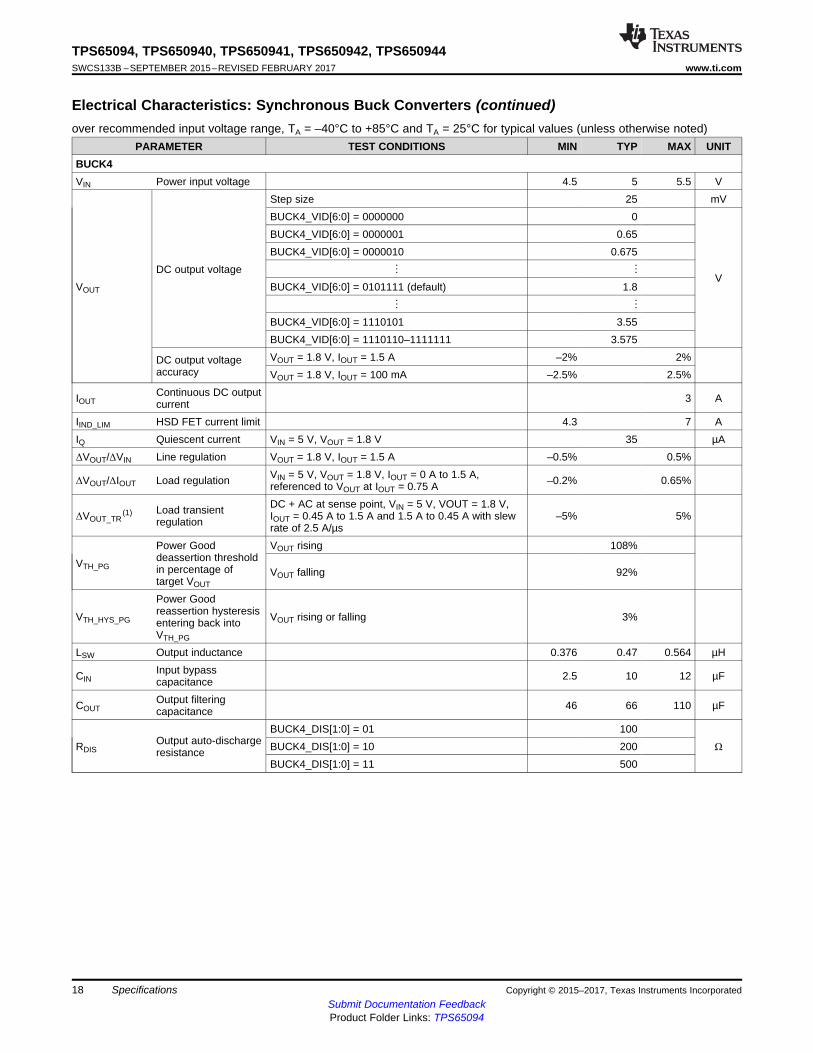
Electrical Characteristics: Synchronous Buck Converters (continued)over recommended input voltage range, TA = –40°C to +85°C and TA = 25°C for typical values (unless otherwise noted)
PARAMETER TEST CONDITIONS MIN TYP MAX UNITBUCK4VIN Power input voltage 4.5 5 5.5 V
VOUT
DC output voltage
Step size 25 mVBUCK4_VID[6:0] = 0000000 0
V
BUCK4_VID[6:0] = 0000001 0.65BUCK4_VID[6:0] = 0000010 0.675
⋮ ⋮BUCK4_VID[6:0] = 0101111 (default) 1.8
⋮ ⋮BUCK4_VID[6:0] = 1110101 3.55BUCK4_VID[6:0] = 1110110–1111111 3.575
DC output voltageaccuracy
VOUT = 1.8 V, IOUT = 1.5 A –2% 2%VOUT = 1.8 V, IOUT = 100 mA –2.5% 2.5%
IOUTContinuous DC outputcurrent 3 A
IIND_LIM HSD FET current limit 4.3 7 AIQ Quiescent current VIN = 5 V, VOUT = 1.8 V 35 µAΔVOUT/ΔVIN Line regulation VOUT = 1.8 V, IOUT = 1.5 A –0.5% 0.5%
ΔVOUT/ΔIOUT Load regulation VIN = 5 V, VOUT = 1.8 V, IOUT = 0 A to 1.5 A,referenced to VOUT at IOUT = 0.75 A –0.2% 0.65%
ΔVOUT_TR(1) Load transient
regulation
DC + AC at sense point, VIN = 5 V, VOUT = 1.8 V,IOUT = 0.45 A to 1.5 A and 1.5 A to 0.45 A with slewrate of 2.5 A/µs
–5% 5%
VTH_PG
Power Gooddeassertion thresholdin percentage oftarget VOUT
VOUT rising 108%
VOUT falling 92%
VTH_HYS_PG
Power Goodreassertion hysteresisentering back intoVTH_PG
VOUT rising or falling 3%
LSW Output inductance 0.376 0.47 0.564 µH
CINInput bypasscapacitance 2.5 10 12 µF
COUTOutput filteringcapacitance 46 66 110 µF
RDISOutput auto-dischargeresistance
BUCK4_DIS[1:0] = 01 100ΩBUCK4_DIS[1:0] = 10 200
BUCK4_DIS[1:0] = 11 500
19
TPS65094, TPS650940, TPS650941, TPS650942, TPS650944www.ti.com SWCS133B –SEPTEMBER 2015–REVISED FEBRUARY 2017
Submit Documentation FeedbackProduct Folder Links: TPS65094
SpecificationsCopyright © 2015–2017, Texas Instruments Incorporated
Electrical Characteristics: Synchronous Buck Converters (continued)over recommended input voltage range, TA = –40°C to +85°C and TA = 25°C for typical values (unless otherwise noted)
PARAMETER TEST CONDITIONS MIN TYP MAX UNITBUCK5VIN Power input voltage 4.5 5 5.5 V
VOUT
DC output voltage
Step size 10 mVBUCK5_VID[6:0] = 0000000 0
V
BUCK5_VID[6:0] = 0000001 0.5BUCK5_VID[6:0] = 0000010 0.51
⋮ ⋮BUCK5_VID[6:0] = 1001011 (default) 1.24
⋮ ⋮BUCK5_VID[6:0] = 1110101 1.66BUCK4_VID[6:0] = 1110110–1111111 1.67
DC output voltageaccuracy
VOUT = 1.24 V, IOUT = 1.5 A –2% 2%VOUT = 1.24 V, IOUT = 100 mA –2.5% 2.5%
IOUTContinuous DC outputcurrent 3.2 A
IIND_LIM HSD FET current limit 4.3 7 AIQ Quiescent current VIN = 5 V, VOUT = 1.24 V 35 µAΔVOUT/ΔVIN Line regulation VOUT = 1.24 V, IOUT = 1.5 A –0.5% 0.5%
ΔVOUT/ΔIOUT Load regulation VIN = 5 V, VOUT = 1.24 V, IOUT = 0 A to 1.5 A,referenced to VOUT at IOUT = 0.75 A –0.2% 1%
ΔVOUT_TR(1) Load transient
regulation
DC + AC at sense point, VIN = 5 V,VOUT = 1.24 V, IOUT = 0.45 A to 1.5 A and 1.5 A to0.45 A with slew rate of 2.5 A/µs
–5% 5%
VTH_PG
Power Gooddeassertion thresholdin percentage oftarget VOUT
VOUT rising 108%
VOUT falling 92%
VTH_HYS_PG
Power Goodreassertion hysteresisentering back intoVTH_PG
VOUT rising or falling 3
LSW Output inductance 0.376 0.47 0.564 µH
CINInput bypasscapacitance 2.5 10 12 µF
COUTOutput filteringcapacitance 31 44 110 µF
RDISOutput auto-dischargeresistance
BUCK5_DIS[1:0] = 01 100ΩBUCK5_DIS[1:0] = 10 200
BUCK5_DIS[1:0] = 11 500
20
TPS65094, TPS650940, TPS650941, TPS650942, TPS650944SWCS133B –SEPTEMBER 2015–REVISED FEBRUARY 2017 www.ti.com
Submit Documentation FeedbackProduct Folder Links: TPS65094
Specifications Copyright © 2015–2017, Texas Instruments Incorporated
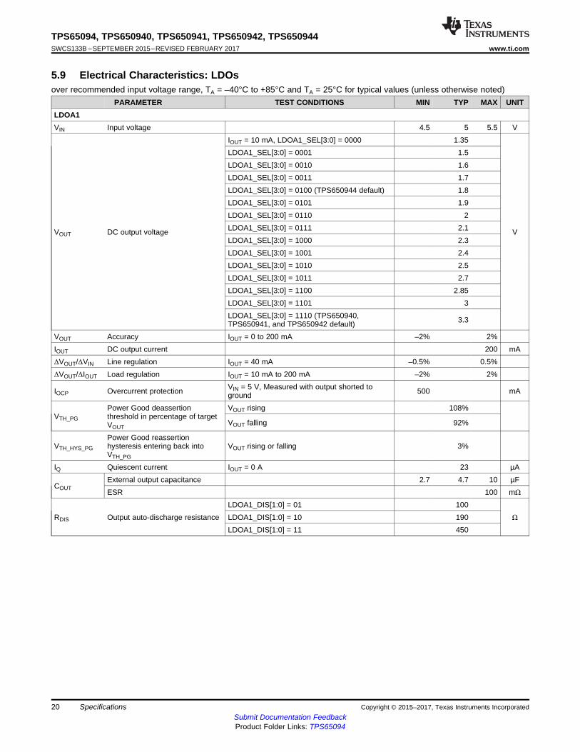
5.9 Electrical Characteristics: LDOsover recommended input voltage range, TA = –40°C to +85°C and TA = 25°C for typical values (unless otherwise noted)
PARAMETER TEST CONDITIONS MIN TYP MAX UNITLDOA1VIN Input voltage 4.5 5 5.5 V
VOUT DC output voltage
IOUT = 10 mA, LDOA1_SEL[3:0] = 0000 1.35
V
LDOA1_SEL[3:0] = 0001 1.5LDOA1_SEL[3:0] = 0010 1.6LDOA1_SEL[3:0] = 0011 1.7LDOA1_SEL[3:0] = 0100 (TPS650944 default) 1.8LDOA1_SEL[3:0] = 0101 1.9LDOA1_SEL[3:0] = 0110 2LDOA1_SEL[3:0] = 0111 2.1LDOA1_SEL[3:0] = 1000 2.3LDOA1_SEL[3:0] = 1001 2.4LDOA1_SEL[3:0] = 1010 2.5LDOA1_SEL[3:0] = 1011 2.7LDOA1_SEL[3:0] = 1100 2.85LDOA1_SEL[3:0] = 1101 3LDOA1_SEL[3:0] = 1110 (TPS650940,TPS650941, and TPS650942 default) 3.3
VOUT Accuracy IOUT = 0 to 200 mA –2% 2%IOUT DC output current 200 mAΔVOUT/ΔVIN Line regulation IOUT = 40 mA –0.5% 0.5%ΔVOUT/ΔIOUT Load regulation IOUT = 10 mA to 200 mA –2% 2%
IOCP Overcurrent protection VIN = 5 V, Measured with output shorted toground 500 mA
VTH_PG
Power Good deassertionthreshold in percentage of targetVOUT
VOUT rising 108%
VOUT falling 92%
VTH_HYS_PG
Power Good reassertionhysteresis entering back intoVTH_PG
VOUT rising or falling 3%
IQ Quiescent current IOUT = 0 A 23 µA
COUTExternal output capacitance 2.7 4.7 10 µFESR 100 mΩ
RDIS Output auto-discharge resistanceLDOA1_DIS[1:0] = 01 100
ΩLDOA1_DIS[1:0] = 10 190LDOA1_DIS[1:0] = 11 450
21
TPS65094, TPS650940, TPS650941, TPS650942, TPS650944www.ti.com SWCS133B –SEPTEMBER 2015–REVISED FEBRUARY 2017
Submit Documentation FeedbackProduct Folder Links: TPS65094
SpecificationsCopyright © 2015–2017, Texas Instruments Incorporated
Electrical Characteristics: LDOs (continued)over recommended input voltage range, TA = –40°C to +85°C and TA = 25°C for typical values (unless otherwise noted)
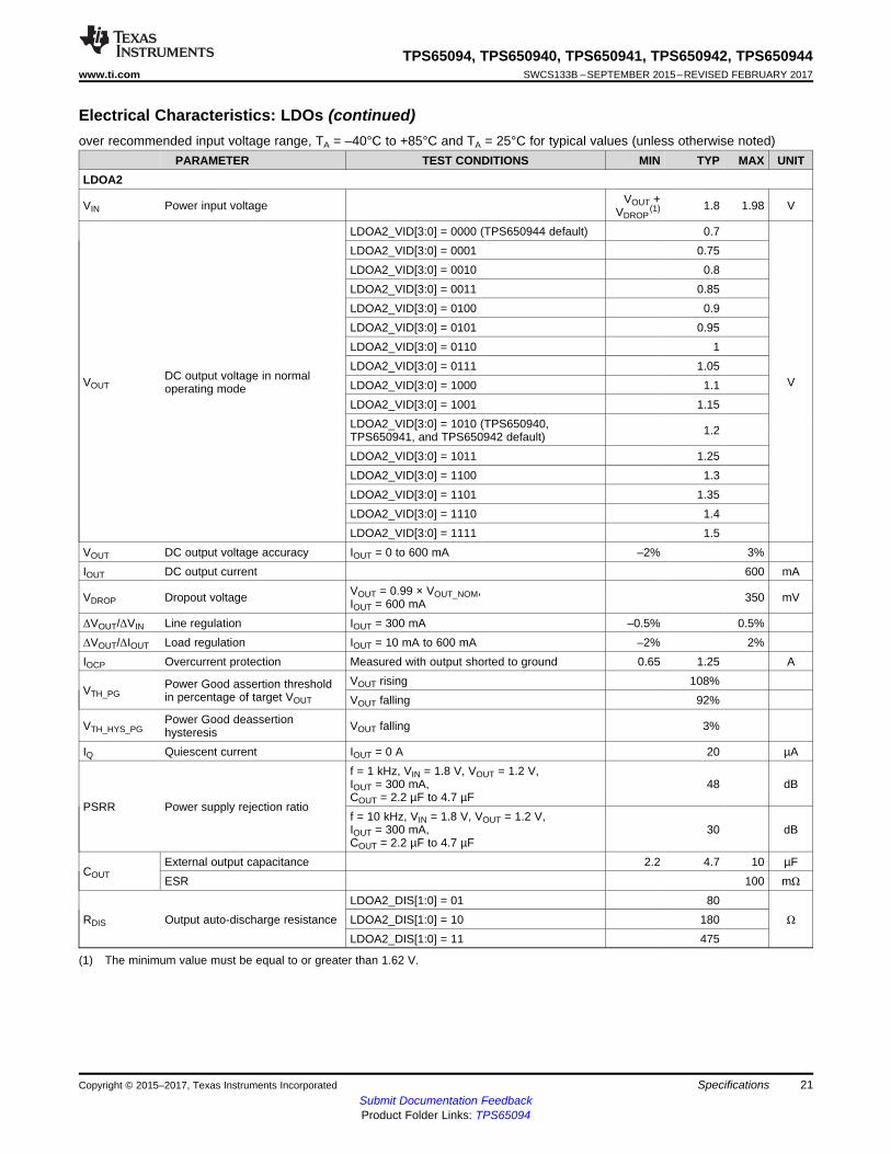
PARAMETER TEST CONDITIONS MIN TYP MAX UNIT
(1) The minimum value must be equal to or greater than 1.62 V.
LDOA2
VIN Power input voltage VOUT +VDROP
(1) 1.8 1.98 V
VOUTDC output voltage in normaloperating mode
LDOA2_VID[3:0] = 0000 (TPS650944 default) 0.7
V
LDOA2_VID[3:0] = 0001 0.75LDOA2_VID[3:0] = 0010 0.8LDOA2_VID[3:0] = 0011 0.85LDOA2_VID[3:0] = 0100 0.9LDOA2_VID[3:0] = 0101 0.95LDOA2_VID[3:0] = 0110 1LDOA2_VID[3:0] = 0111 1.05LDOA2_VID[3:0] = 1000 1.1LDOA2_VID[3:0] = 1001 1.15LDOA2_VID[3:0] = 1010 (TPS650940,TPS650941, and TPS650942 default) 1.2
LDOA2_VID[3:0] = 1011 1.25LDOA2_VID[3:0] = 1100 1.3LDOA2_VID[3:0] = 1101 1.35LDOA2_VID[3:0] = 1110 1.4LDOA2_VID[3:0] = 1111 1.5
VOUT DC output voltage accuracy IOUT = 0 to 600 mA –2% 3%IOUT DC output current 600 mA
VDROP Dropout voltage VOUT = 0.99 × VOUT_NOM,IOUT = 600 mA 350 mV
ΔVOUT/ΔVIN Line regulation IOUT = 300 mA –0.5% 0.5%ΔVOUT/ΔIOUT Load regulation IOUT = 10 mA to 600 mA –2% 2%IOCP Overcurrent protection Measured with output shorted to ground 0.65 1.25 A
VTH_PGPower Good assertion thresholdin percentage of target VOUT
VOUT rising 108%VOUT falling 92%
VTH_HYS_PGPower Good deassertionhysteresis VOUT falling 3%
IQ Quiescent current IOUT = 0 A 20 µA
PSRR Power supply rejection ratio
f = 1 kHz, VIN = 1.8 V, VOUT = 1.2 V,IOUT = 300 mA,COUT = 2.2 µF to 4.7 µF
48 dB
f = 10 kHz, VIN = 1.8 V, VOUT = 1.2 V,IOUT = 300 mA,COUT = 2.2 µF to 4.7 µF
30 dB
COUTExternal output capacitance 2.2 4.7 10 µFESR 100 mΩ
RDIS Output auto-discharge resistanceLDOA2_DIS[1:0] = 01 80
ΩLDOA2_DIS[1:0] = 10 180LDOA2_DIS[1:0] = 11 475
22
TPS65094, TPS650940, TPS650941, TPS650942, TPS650944SWCS133B –SEPTEMBER 2015–REVISED FEBRUARY 2017 www.ti.com
Submit Documentation FeedbackProduct Folder Links: TPS65094
Specifications Copyright © 2015–2017, Texas Instruments Incorporated
Electrical Characteristics: LDOs (continued)over recommended input voltage range, TA = –40°C to +85°C and TA = 25°C for typical values (unless otherwise noted)
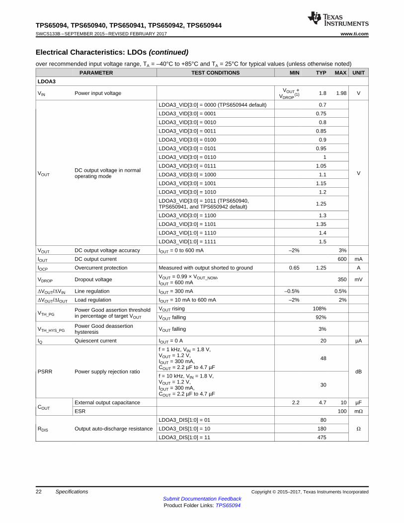
PARAMETER TEST CONDITIONS MIN TYP MAX UNITLDOA3
VIN Power input voltage VOUT +VDROP
(1) 1.8 1.98 V
VOUTDC output voltage in normaloperating mode
LDOA3_VID[3:0] = 0000 (TPS650944 default) 0.7
V
LDOA3_VID[3:0] = 0001 0.75LDOA3_VID[3:0] = 0010 0.8LDOA3_VID[3:0] = 0011 0.85LDOA3_VID[3:0] = 0100 0.9LDOA3_VID[3:0] = 0101 0.95LDOA3_VID[3:0] = 0110 1LDOA3_VID[3:0] = 0111 1.05LDOA3_VID[3:0] = 1000 1.1LDOA3_VID[3:0] = 1001 1.15LDOA3_VID[3:0] = 1010 1.2LDOA3_VID[3:0] = 1011 (TPS650940,TPS650941, and TPS650942 default) 1.25
LDOA3_VID[3:0] = 1100 1.3LDOA3_VID[3:0] = 1101 1.35LDOA3_VID[1:0] = 1110 1.4LDOA3_VID[1:0] = 1111 1.5
VOUT DC output voltage accuracy IOUT = 0 to 600 mA –2% 3%IOUT DC output current 600 mAIOCP Overcurrent protection Measured with output shorted to ground 0.65 1.25 A
VDROP Dropout voltage VOUT = 0.99 × VOUT_NOM,IOUT = 600 mA 350 mV
ΔVOUT/ΔVIN Line regulation IOUT = 300 mA –0.5% 0.5%ΔVOUT/ΔIOUT Load regulation IOUT = 10 mA to 600 mA –2% 2%
VTH_PGPower Good assertion thresholdin percentage of target VOUT
VOUT rising 108%VOUT falling 92%
VTH_HYS_PGPower Good deassertionhysteresis VOUT falling 3%
IQ Quiescent current IOUT = 0 A 20 µA
PSRR Power supply rejection ratio
f = 1 kHz, VIN = 1.8 V,VOUT = 1.2 V,IOUT = 300 mA,COUT = 2.2 µF to 4.7 µF
48
dBf = 10 kHz, VIN = 1.8 V,VOUT = 1.2 V,IOUT = 300 mA,COUT = 2.2 µF to 4.7 µF
30
COUTExternal output capacitance 2.2 4.7 10 µFESR 100 mΩ
RDIS Output auto-discharge resistanceLDOA3_DIS[1:0] = 01 80
ΩLDOA3_DIS[1:0] = 10 180LDOA3_DIS[1:0] = 11 475
23
TPS65094, TPS650940, TPS650941, TPS650942, TPS650944www.ti.com SWCS133B –SEPTEMBER 2015–REVISED FEBRUARY 2017
Submit Documentation FeedbackProduct Folder Links: TPS65094
SpecificationsCopyright © 2015–2017, Texas Instruments Incorporated
Electrical Characteristics: LDOs (continued)over recommended input voltage range, TA = –40°C to +85°C and TA = 25°C for typical values (unless otherwise noted)
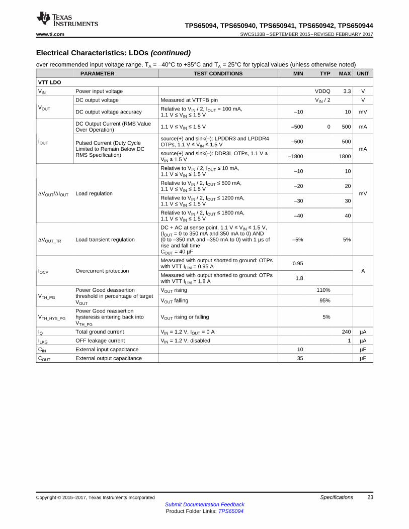
PARAMETER TEST CONDITIONS MIN TYP MAX UNITVTT LDOVIN Power input voltage VDDQ 3.3 V
VOUT
DC output voltage Measured at VTTFB pin VIN / 2 V
DC output voltage accuracy Relative to VIN / 2, IOUT = 100 mA,1.1 V ≤ VIN ≤ 1.5 V –10 10 mV
IOUT
DC Output Current (RMS ValueOver Operation) 1.1 V ≤ VIN ≤ 1.5 V –500 0 500 mA
Pulsed Current (Duty CycleLimited to Remain Below DCRMS Specification)
source(+) and sink(–): LPDDR3 and LPDDR4OTPs, 1.1 V ≤ VIN ≤ 1.5 V –500 500
mAsource(+) and sink(–): DDR3L OTPs, 1.1 V ≤VIN ≤ 1.5 V –1800 1800
ΔVOUT/ΔIOUT Load regulation
Relative to VIN / 2, IOUT ≤ 10 mA,1.1 V ≤ VIN ≤ 1.5 V –10 10
mV
Relative to VIN / 2, IOUT ≤ 500 mA,1.1 V ≤ VIN ≤ 1.5 V –20 20
Relative to VIN / 2, IOUT ≤ 1200 mA,1.1 V ≤ VIN ≤ 1.5 V –30 30
Relative to VIN / 2, IOUT ≤ 1800 mA,1.1 V ≤ VIN ≤ 1.5 V –40 40
ΔVOUT_TR Load transient regulation
DC + AC at sense point, 1.1 V ≤ VIN ≤ 1.5 V,(IOUT = 0 to 350 mA and 350 mA to 0) AND(0 to –350 mA and –350 mA to 0) with 1 µs ofrise and fall timeCOUT = 40 µF
–5% 5%
IOCP Overcurrent protection
Measured with output shorted to ground: OTPswith VTT ILIM = 0.95 A 0.95
AMeasured with output shorted to ground: OTPswith VTT ILIM = 1.8 A 1.8
VTH_PG
Power Good deassertionthreshold in percentage of targetVOUT
VOUT rising 110%
VOUT falling 95%
VTH_HYS_PG
Power Good reassertionhysteresis entering back intoVTH_PG
VOUT rising or falling 5%
IQ Total ground current VIN = 1.2 V, IOUT = 0 A 240 µAILKG OFF leakage current VIN = 1.2 V, disabled 1 µACIN External input capacitance 10 µFCOUT External output capacitance 35 µF
24
TPS65094, TPS650940, TPS650941, TPS650942, TPS650944SWCS133B –SEPTEMBER 2015–REVISED FEBRUARY 2017 www.ti.com
Submit Documentation FeedbackProduct Folder Links: TPS65094
Specifications Copyright © 2015–2017, Texas Instruments Incorporated
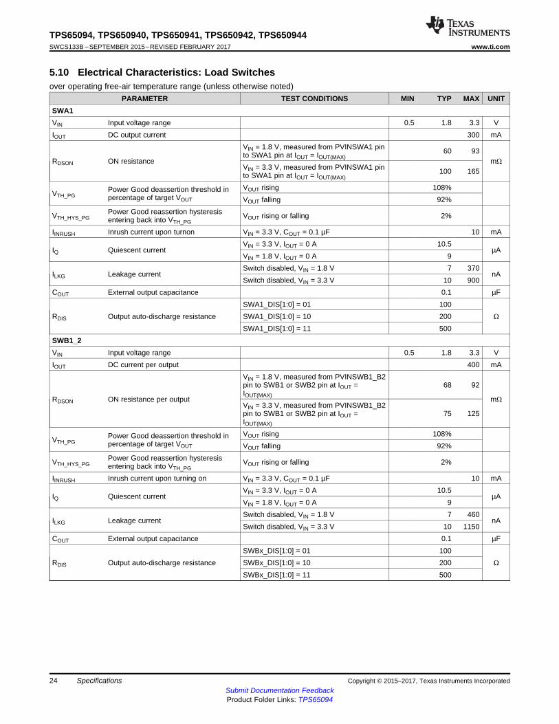
5.10 Electrical Characteristics: Load Switchesover operating free-air temperature range (unless otherwise noted)
PARAMETER TEST CONDITIONS MIN TYP MAX UNITSWA1VIN Input voltage range 0.5 1.8 3.3 VIOUT DC output current 300 mA
RDSON ON resistance
VIN = 1.8 V, measured from PVINSWA1 pinto SWA1 pin at IOUT = IOUT(MAX)
60 93mΩ
VIN = 3.3 V, measured from PVINSWA1 pinto SWA1 pin at IOUT = IOUT(MAX)
100 165
VTH_PGPower Good deassertion threshold inpercentage of target VOUT
VOUT rising 108%VOUT falling 92%
VTH_HYS_PGPower Good reassertion hysteresisentering back into VTH_PG
VOUT rising or falling 2%
IINRUSH Inrush current upon turnon VIN = 3.3 V, COUT = 0.1 µF 10 mA
IQ Quiescent currentVIN = 3.3 V, IOUT = 0 A 10.5
µAVIN = 1.8 V, IOUT = 0 A 9
ILKG Leakage currentSwitch disabled, VIN = 1.8 V 7 370
nASwitch disabled, VIN = 3.3 V 10 900
COUT External output capacitance 0.1 µF
RDIS Output auto-discharge resistanceSWA1_DIS[1:0] = 01 100
ΩSWA1_DIS[1:0] = 10 200SWA1_DIS[1:0] = 11 500
SWB1_2VIN Input voltage range 0.5 1.8 3.3 VIOUT DC current per output 400 mA
RDSON ON resistance per output
VIN = 1.8 V, measured from PVINSWB1_B2pin to SWB1 or SWB2 pin at IOUT =IOUT(MAX)
68 92
mΩVIN = 3.3 V, measured from PVINSWB1_B2pin to SWB1 or SWB2 pin at IOUT =IOUT(MAX)
75 125
VTH_PGPower Good deassertion threshold inpercentage of target VOUT
VOUT rising 108%VOUT falling 92%
VTH_HYS_PGPower Good reassertion hysteresisentering back into VTH_PG
VOUT rising or falling 2%
IINRUSH Inrush current upon turning on VIN = 3.3 V, COUT = 0.1 µF 10 mA
IQ Quiescent currentVIN = 3.3 V, IOUT = 0 A 10.5
µAVIN = 1.8 V, IOUT = 0 A 9
ILKG Leakage currentSwitch disabled, VIN = 1.8 V 7 460
nASwitch disabled, VIN = 3.3 V 10 1150
COUT External output capacitance 0.1 µF
RDIS Output auto-discharge resistanceSWBx_DIS[1:0] = 01 100
ΩSWBx_DIS[1:0] = 10 200SWBx_DIS[1:0] = 11 500
25
TPS65094, TPS650940, TPS650941, TPS650942, TPS650944www.ti.com SWCS133B –SEPTEMBER 2015–REVISED FEBRUARY 2017
Submit Documentation FeedbackProduct Folder Links: TPS65094
SpecificationsCopyright © 2015–2017, Texas Instruments Incorporated
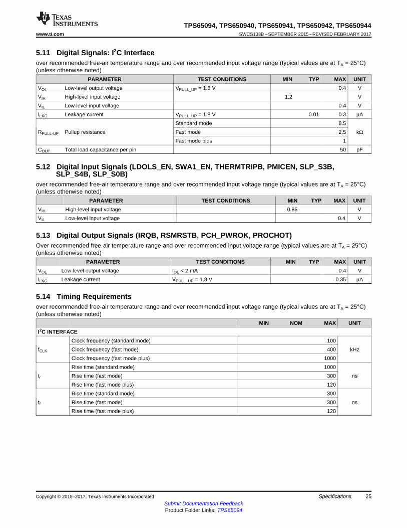
5.11 Digital Signals: I2C Interfaceover recommended free-air temperature range and over recommended input voltage range (typical values are at TA = 25°C)(unless otherwise noted)
PARAMETER TEST CONDITIONS MIN TYP MAX UNITVOL Low-level output voltage VPULL_UP = 1.8 V 0.4 VVIH High-level input voltage 1.2 VVIL Low-level input voltage 0.4 VILKG Leakage current VPULL_UP = 1.8 V 0.01 0.3 µA
RPULL-UP Pullup resistanceStandard mode 8.5
kΩFast mode 2.5Fast mode plus 1
COUT Total load capacitance per pin 50 pF
5.12 Digital Input Signals (LDOLS_EN, SWA1_EN, THERMTRIPB, PMICEN, SLP_S3B,SLP_S4B, SLP_S0B)
over recommended free-air temperature range and over recommended input voltage range (typical values are at TA = 25°C)(unless otherwise noted)
PARAMETER TEST CONDITIONS MIN TYP MAX UNITVIH High-level input voltage 0.85 VVIL Low-level input voltage 0.4 V
5.13 Digital Output Signals (IRQB, RSMRSTB, PCH_PWROK, PROCHOT)Over recommended free-air temperature range and over recommended input voltage range (typical values are at TA = 25°C)(unless otherwise noted)
PARAMETER TEST CONDITIONS MIN TYP MAX UNITVOL Low-level output voltage IOL < 2 mA 0.4 VILKG Leakage current VPULL_UP = 1.8 V 0.35 µA
5.14 Timing Requirementsover recommended free-air temperature range and over recommended input voltage range (typical values are at TA = 25°C)(unless otherwise noted)
MIN NOM MAX UNITI2C INTERFACE
fCLK
Clock frequency (standard mode) 100kHzClock frequency (fast mode) 400
Clock frequency (fast mode plus) 1000
tr
Rise time (standard mode) 1000nsRise time (fast mode) 300
Rise time (fast mode plus) 120
tf
Rise time (standard mode) 300nsRise time (fast mode) 300
Rise time (fast mode plus) 120
26
TPS65094, TPS650940, TPS650941, TPS650942, TPS650944SWCS133B –SEPTEMBER 2015–REVISED FEBRUARY 2017 www.ti.com
Submit Documentation FeedbackProduct Folder Links: TPS65094
Specifications Copyright © 2015–2017, Texas Instruments Incorporated
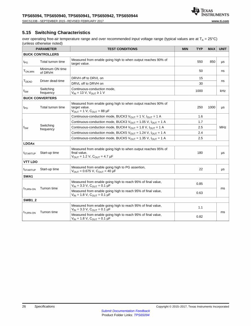
5.15 Switching Characteristicsover operating free-air temperature range and over recommended input voltage range (typical values are at TA = 25°C)(unless otherwise noted)
PARAMETER TEST CONDITIONS MIN TYP MAX UNITBUCK CONTROLLERS
tPG Total turnon time Measured from enable going high to when output reaches 90% oftarget value. 550 850 µs
TON,MINMinimum ON timeof DRVH 50 ns
TDEAD Driver dead-timeDRVH off to DRVL on 15
nsDRVL off to DRVH on 30
fSWSwitchingfrequency
Continuous-conduction mode,VIN = 13 V, VOUT ≥ 1 V 1000 kHz
BUCK CONVERTERS
tPG Total turnon timeMeasured from enable going high to when output reaches 90% oftarget value.VOUT = 1 V, COUT = 88 µF
250 1000 µs
fSWSwitchingfrequency
Continuous-conduction mode, BUCK3 VOUT = 1 V, IOUT = 1 A 1.6
MHzContinuous-conduction mode, BUCK3 VOUT = 1.05 V, IOUT = 1 A 1.7Continuous-conduction mode, BUCK4 VOUT = 1.8 V, IOUT = 1 A 2.5Continuous-conduction mode, BUCK5 VOUT = 1.24 V, IOUT = 1 A 2.4Continuous-conduction mode, BUCK5 VOUT = 1.35 V, IOUT = 1 A 2.5
LDOAx
tSTARTUP Start-up timeMeasured from enable going high to when output reaches 95% offinal value,VOUT = 1.2 V, COUT = 4.7 µF
180 µs
VTT LDO
tSTARTUP Start-up time Measured from enable going high to PG assertion,VOUT = 0.675 V, COUT = 40 µF 22 µs
SWA1
tTURN-ON Turnon time
Measured from enable going high to reach 95% of final value,VIN = 3.3 V, COUT = 0.1 µF 0.85
msMeasured from enable going high to reach 95% of final value,VIN = 1.8 V, COUT = 0.1 µF 0.63
SWB1_2
tTURN-ON Turnon time
Measured from enable going high to reach 95% of final value,VIN = 3.3 V, COUT = 0.1 µF 1.1
msMeasured from enable going high to reach 95% of final value,VIN = 1.8 V, COUT = 0.1 µF 0.82
Output Load (A)
Effi
cien
cy
0 0.25 0.5 0.75 1 1.25 1.583%
84%
85%
86%
87%
88%
89%
90%
91%
D004
VSYS = 4.5 VVSYS = 5 VVSYS = 5.5 V
Output Load (A)
Effi
cien
cy
0 0.25 0.5 0.75 1 1.25 1.580%
81%
82%
83%
84%
85%
86%
87%
88%
89%
90%
D005
VSYS = 4.5 VVSYS = 5 VVSYS = 5.5 V
Output Load (A)
Effi
cien
cy
0 1 2 3 4 5 6 776%
78%
80%
82%
84%
86%
88%
90%
92%
D011
VSYS = 5.4 VVSYS = 13 VVSYS = 18 V
Output Load (A)
Effi
cien
cy
0 0.5 1 1.5 2 2.5 369%
71%
73%
75%
77%
79%
81%
83%
85%
87%
89%
D003
VSYS = 4.5 VVSYS = 5 VVSYS = 5.5 V
Output Load (A)
Effi
cien
cy
0 0.5 1 1.5 2 2.5 3 3.5 4 4.5 568%
70%
72%
74%
76%
78%
80%
82%
84%
86%
88%
D001
VSYS = 5.4 VVSYS = 13 VVSYS = 18 V
Output Load (A)
Effi
cien
cy
0 3 6 9 12 15 18 2170%
72%
74%
76%
78%
80%
82%
84%
86%
88%
D002
VSYS = 5.4 VVSYS = 13 VVSYS = 18 V
27
TPS65094, TPS650940, TPS650941, TPS650942, TPS650944www.ti.com SWCS133B –SEPTEMBER 2015–REVISED FEBRUARY 2017
Submit Documentation FeedbackProduct Folder Links: TPS65094
SpecificationsCopyright © 2015–2017, Texas Instruments Incorporated
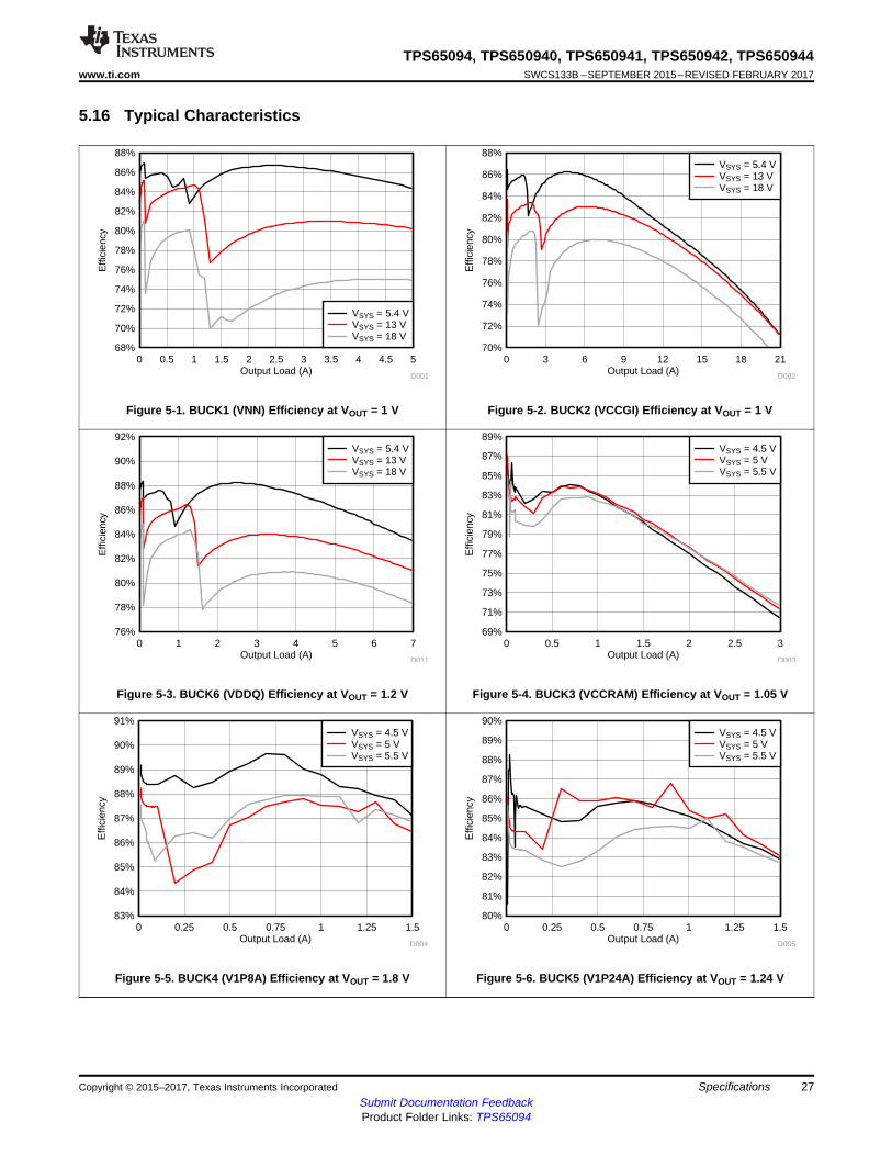
5.16 Typical Characteristics
Figure 5-1. BUCK1 (VNN) Efficiency at VOUT = 1 V Figure 5-2. BUCK2 (VCCGI) Efficiency at VOUT = 1 V
Figure 5-3. BUCK6 (VDDQ) Efficiency at VOUT = 1.2 V Figure 5-4. BUCK3 (VCCRAM) Efficiency at VOUT = 1.05 V
Figure 5-5. BUCK4 (V1P8A) Efficiency at VOUT = 1.8 V Figure 5-6. BUCK5 (V1P24A) Efficiency at VOUT = 1.24 V
28
TPS65094, TPS650940, TPS650941, TPS650942, TPS650944SWCS133B –SEPTEMBER 2015–REVISED FEBRUARY 2017 www.ti.com
Submit Documentation FeedbackProduct Folder Links: TPS65094
Detailed Description Copyright © 2015–2017, Texas Instruments Incorporated
(1) When powered from a 5-V supply through the DRV5V_2_A1 pin. Otherwise, maximum current is limited by maximum IOUT of LDO5.(2) For LPDDR3 and LPDDR4 memory, SWB1_2 is configured to V1P8U and controlled by SLP_S4B. For DDR3L memory, SWB1_2 is
configured to either V3P3S or V1P8S and controlled by SLP_S3B.
6 Detailed Description
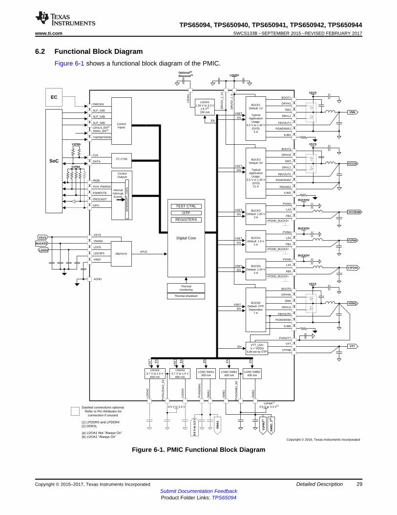
6.1 OverviewThe TPS65094x device provides all the necessary power supplies for the Intel Reference Designs. For anoverview of the different OTP configurations, consult Table 3-1. The following VRs are integrated: threestep-down controllers (BUCK1, BUCK2, and BUCK6), three step-down converters (BUCK3, BUCK4, andBUCK5), a sink and source LDO (VTT LDO), three low-voltage VIN LDOs (LDOA1–LDOA3), and threeload switches that are managed by power-up sequence logic to provide the proper power rails,sequencing, and protection. All VRs have a built-in discharge resistor, and the value can be changed bythe DISCHCNT1–DISCHCNT3 and LDOA1_CTRL registers. When enabling a VR, the PMIC automaticallydisconnects the discharge resistor for that rail without any I2C command. Table 6-1 summarizes the keycharacteristics of the voltage rails.
Table 6-1. Summary of Voltage Regulators
RAIL TYPEINPUT VOLTAGE
(V)OUTPUT VOLTAGE RANGE
(V)TYPICAL
APPLICATIONCURRENT
(mA)MIN MAX MIN TYP MAX
BUCK1 (VNN) Step-down controller 4.5 21 0.5 1.05 1.67 5000BUCK2 (VCCGI) Step-down controller 4.5 21 0.5 1 1.67 21000BUCK3(VCCRAM) Step-down converter 4.5 5.5 0.65 1.05 3.575 3000
BUCK4 (V1P8A) Step-down converter 4.5 5.5 0.65 1.8 3.575 1500BUCK5 (V1P24A) Step-down converter 4.5 5.5 0.5 1.24 1.67 1900BUCK6 (VDDQ) Step-down controller 4.5 21 0.5 OTP dependent 1.67 7000LDOA1 LDO 4.5 5.5 1.35 OTP dependent 3.3 200 (1)
LDOA2 LDO 1.62 1.98 0.7 OTP dependent 1.5 600LDOA3 LDO 1.62 1.98 0.7 OTP dependent 1.5 600SWA1 Load switch 0.5 3.3 300SWB1_2 (2) Load switch 0.5 3.3 800 (combined)
VTT Sink and sourceLDO BUCK6 output VBUCK6 / 2 OTP dependent
IRQB
ControlOutputs
REFSYS
REGISTERS
Digital Core
INT
ER
RU
PT
_CN
TL
Thermalmonitoring
Thermal shutdown
OTP
TEST CTRL
I2C CTRL
SLP_S0B
PCH_PWROK
RSMRSTB
PROCHOT
InternalInterrupt Events
<PGND_BUCK3>
BUCK3Default: 1.05 V
3 A
VREF
BUCK1Default: 1V
Typical Application
Usage:0.5 V to 1.45 V
(DVS)5 A
VSYS
LDOA20.7 V to 1.5 V
600 mA
ControlInputs
SoC
VSYS
LOAD SWB2400 mA
PMICEN
SLP_S3B
SLP_S4B
LDOLS_EN(a)
SWA1_EN(b)
THERMTRIPB
VSYS
LDO5
LDO3P3
V5ANABUCK5V
nPUC
BOOT1
DRVH1
SW1
DRVL1
FBVOUT1
PGNDSNS1
ILIM1
BUCK2Default: 0V
Typical Application
Usage:0.5 V to 1.45 V
(DVS)21 A
VSYS
BOOT2
DRVH2
SW2
DRVL2
FBVOUT2
PGNDSNS2
ILIM2
PVIN3
LX3
FB3
BUCK5V
<PGND_BUCK4>
BUCK4Default: 1.8 V
2 A
PVIN4
LX4
FB4
<PGND_BUCK5>
BUCK5Default: 1.24 V
2 A
PVIN5
LX5
FB5
BUCK5V
BUCK6Default: OTP Dependent
7 A
VSYS
BOOT6
DRVH6
SW6
DRVL6
FBVOUT6
PGNDSNS6
ILIM6
LDO5V
VNN
VTT_LDO½ × VDDQ
ILIM set by OTP
VDDQ
VTT
PVINVTT
VTT
VTTFB
DR
V5V
_1_6
DR
V5V
_2_A
1
LDOA11.35 V to 3.3 V
1.8 V(b)
200 mA
LDO
A1
V1P8A
CLK
DATA
LOAD SWB1400 mA
LOAD SWA1300 mA
LDOA30.7 V to 1.5 V
600 mA
SW
B2
PV
INS
WB
1_B
2
SW
B1
SW
A1
PV
INS
WA
1
LDO
A3
PV
INLD
OA
2_A
3
LDO
A2
AGND
0.5
V t
o 3
.3 V
V1P
8U(1
)
SW
A1
VCCGI
VCCRAM
V1P8A
V1P24A
FBGND2
VSET
EN
VSET
EN
VSET
EN
VSET
EN
VSET
EN
VSET
EN
VS
ET
EN
VS
ET
EN
EN
EN
EN
EN
EN
LDO5V
BUCK5V
EC
0.5 V to 3.3 V
V1P8A
GPO
Dashed connections optional.Refer to Pin Attributes for
connection if unused.
SW
B1_
2(2)
(1) LPDDR3 and LPDDR4(2) DDR3L
(a) LDOA1 1RW�³$OZD\V�2Q´(b) LDOA1 ³$OZD\V�2Q´
Optional(a)
Required(b)
V1P8A(1)
0.5 V to 3.3 V(2)
Copyright © 2016, Texas Instruments Incorporated
29
TPS65094, TPS650940, TPS650941, TPS650942, TPS650944www.ti.com SWCS133B –SEPTEMBER 2015–REVISED FEBRUARY 2017
Submit Documentation FeedbackProduct Folder Links: TPS65094
Detailed DescriptionCopyright © 2015–2017, Texas Instruments Incorporated
6.2 Functional Block DiagramFigure 6-1 shows a functional block diagram of the PMIC.
Figure 6-1. PMIC Functional Block Diagram
BUCK1 5 A
BUCK2 21 A
BUCK3 3 A
BUCK4 2 A
BUCK5 2 A
BUCK6 7 A
VTT LDO 1.5 A
LDOA2 0.6 A
LDOA3 0.6 A
SWA1 0.3 A
SWB1 0.4 A
SWB2 0.4 A
LDOA1 0.2 A
LDO5 0.18 A
LDO3P3 0.04 A
PG_5V
PMICENSLP_S3B
IRQB
SCLK
DATA
RSMRSTB
PCH_PWROK
SLP_S4B
SLP_S0B
EXT FET
EXT FET
EXT FET
VNN
VCCGI
VCCRAM
V1P8A
V1P24A
VDDQ
VTT
0.7 V to 1.5 V
0.7 V to 1.5 V
0.5 V to 3.3 V
V1P8U(1)
0.5 V to 3.3 V(2)
PMIC SoC PLATFORM
VDDQVSYS
VSYS
BUCK
5 V
VSYS
LDO5P0
V1P8A
VSYS
LDO5P0
BUCK
3.3 V
+REF
THERMTRIPB
PROCHOT
800 mA
1.35 V to 3.3 V(a)
1.8 V(b)
LDOLS_EN(a)
SWA1_EN(b)
(a) LDOA1 1RW�³$OZD\V�2Q´(b) LDOA1 ³$OZD\V�2Q´
(1) LPDDR3 and LPDDR4(2) DDR3L
0.5 V to 3.3 V
V1P8A(1)
0.5 V to 3.3 V(2)
VSYS
Copyright © 2016, Texas Instruments Incorporated
30
TPS65094, TPS650940, TPS650941, TPS650942, TPS650944SWCS133B –SEPTEMBER 2015–REVISED FEBRUARY 2017 www.ti.com
Submit Documentation FeedbackProduct Folder Links: TPS65094
Detailed Description Copyright © 2015–2017, Texas Instruments Incorporated
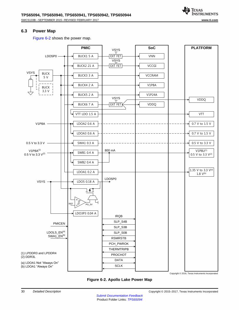
6.3 Power MapFigure 6-2 shows the power map.
Figure 6-2. Apollo Lake Power Map
31
TPS65094, TPS650940, TPS650941, TPS650942, TPS650944www.ti.com SWCS133B –SEPTEMBER 2015–REVISED FEBRUARY 2017
Submit Documentation FeedbackProduct Folder Links: TPS65094
Detailed DescriptionCopyright © 2015–2017, Texas Instruments Incorporated
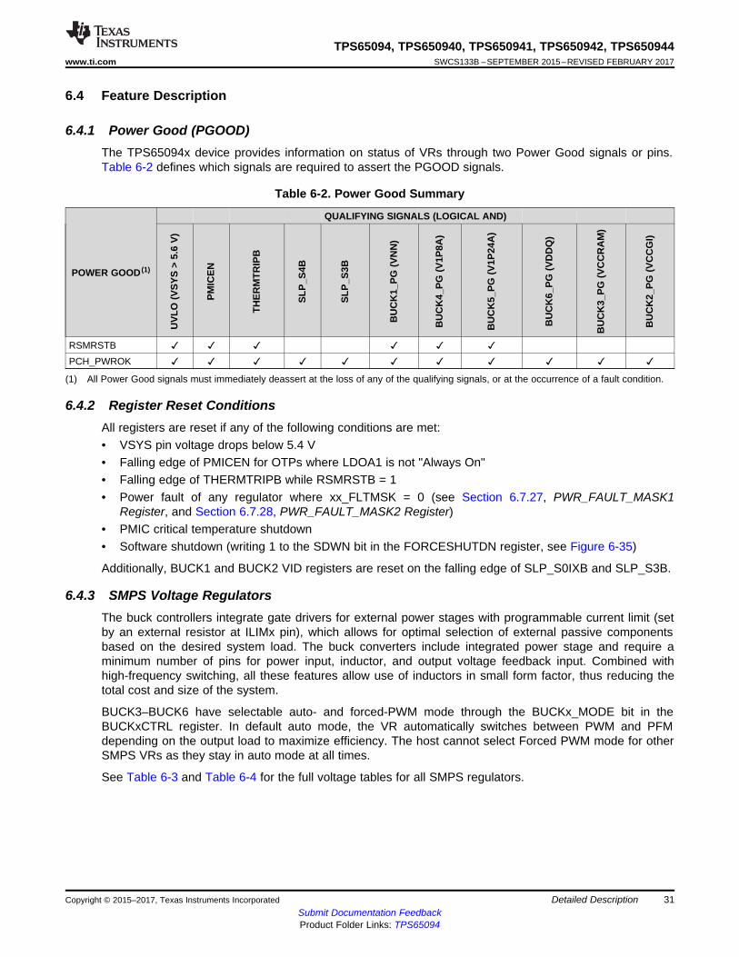
(1) All Power Good signals must immediately deassert at the loss of any of the qualifying signals, or at the occurrence of a fault condition.
6.4 Feature Description
6.4.1 Power Good (PGOOD)The TPS65094x device provides information on status of VRs through two Power Good signals or pins.Table 6-2 defines which signals are required to assert the PGOOD signals.
Table 6-2. Power Good Summary
POWER GOOD (1)
QUALIFYING SIGNALS (LOGICAL AND)
UVL
O(V
SYS
>5.
6V)
PMIC
EN
THER
MTR
IPB
SLP_
S4B
SLP_
S3B
BU
CK
1_PG
(VN
N)
BU
CK
4_PG
(V1P
8A)
BU
CK
5_PG
(V1P
24A
)
BU
CK
6_PG
(VD
DQ
)
BU
CK
3_PG
(VC
CR
AM
)
BU
CK
2_PG
(VC
CG
I)
RSMRSTB ✓ ✓ ✓ ✓ ✓ ✓PCH_PWROK ✓ ✓ ✓ ✓ ✓ ✓ ✓ ✓ ✓ ✓ ✓
6.4.2 Register Reset ConditionsAll registers are reset if any of the following conditions are met:• VSYS pin voltage drops below 5.4 V• Falling edge of PMICEN for OTPs where LDOA1 is not "Always On"• Falling edge of THERMTRIPB while RSMRSTB = 1• Power fault of any regulator where xx_FLTMSK = 0 (see Section 6.7.27, PWR_FAULT_MASK1
Register, and Section 6.7.28, PWR_FAULT_MASK2 Register)• PMIC critical temperature shutdown• Software shutdown (writing 1 to the SDWN bit in the FORCESHUTDN register, see Figure 6-35)
Additionally, BUCK1 and BUCK2 VID registers are reset on the falling edge of SLP_S0IXB and SLP_S3B.
6.4.3 SMPS Voltage RegulatorsThe buck controllers integrate gate drivers for external power stages with programmable current limit (setby an external resistor at ILIMx pin), which allows for optimal selection of external passive componentsbased on the desired system load. The buck converters include integrated power stage and require aminimum number of pins for power input, inductor, and output voltage feedback input. Combined withhigh-frequency switching, all these features allow use of inductors in small form factor, thus reducing thetotal cost and size of the system.
BUCK3–BUCK6 have selectable auto- and forced-PWM mode through the BUCKx_MODE bit in theBUCKxCTRL register. In default auto mode, the VR automatically switches between PWM and PFMdepending on the output load to maximize efficiency. The host cannot select Forced PWM mode for otherSMPS VRs as they stay in auto mode at all times.
See Table 6-3 and Table 6-4 for the full voltage tables for all SMPS regulators.
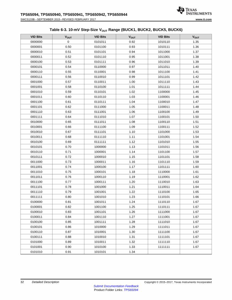
32
TPS65094, TPS650940, TPS650941, TPS650942, TPS650944SWCS133B –SEPTEMBER 2015–REVISED FEBRUARY 2017 www.ti.com
Submit Documentation FeedbackProduct Folder Links: TPS65094
Detailed Description Copyright © 2015–2017, Texas Instruments Incorporated
Table 6-3. 10-mV Step-Size VOUT Range (BUCK1, BUCK2, BUCK5, BUCK6)
VID Bits VOUT VID Bits VOUT VID Bits VOUT
0000000 0 0101011 0.92 1010110 1.350000001 0.50 0101100 0.93 1010111 1.360000010 0.51 0101101 0.94 1011000 1.370000011 0.52 0101110 0.95 1011001 1.380000100 0.53 0101111 0.96 1011010 1.390000101 0.54 0110000 0.97 1011011 1.400000110 0.55 0110001 0.98 1011100 1.410000111 0.56 0110010 0.99 1011101 1.420001000 0.57 0110011 1.00 1011110 1.430001001 0.58 0110100 1.01 1011111 1.440001010 0.59 0110101 1.02 1100000 1.450001011 0.60 0110110 1.03 1100001 1.460001100 0.61 0110111 1.04 1100010 1.470001101 0.62 0111000 1.05 1100011 1.480001110 0.63 0111001 1.06 1100100 1.490001111 0.64 0111010 1.07 1100101 1.500010000 0.65 0111011 1.08 1100110 1.510010001 0.66 0111100 1.09 1100111 1.520010010 0.67 0111101 1.10 1101000 1.530010011 0.68 0111110 1.11 1101001 1.540010100 0.69 0111111 1.12 1101010 1.550010101 0.70 1000000 1.13 1101011 1.560010110 0.71 1000001 1.14 1101100 1.570010111 0.72 1000010 1.15 1101101 1.580011000 0.73 1000011 1.16 1101110 1.590011001 0.74 1000100 1.17 1101111 1.600011010 0.75 1000101 1.18 1110000 1.610011011 0.76 1000110 1.19 1110001 1.620011100 0.77 1000111 1.20 1110010 1.630011101 0.78 1001000 1.21 1110011 1.640011110 0.79 1001001 1.22 1110100 1.650011111 0.80 1001010 1.23 1110101 1.660100000 0.81 1001011 1.24 1110110 1.670100001 0.82 1001100 1.25 1110111 1.670100010 0.83 1001101 1.26 1111000 1.670100011 0.84 1001110 1.27 1111001 1.670100100 0.85 1001111 1.28 1111010 1.670100101 0.86 1010000 1.29 1111011 1.670100110 0.87 1010001 1.30 1111100 1.670100111 0.88 1010010 1.31 1111101 1.670101000 0.89 1010011 1.32 1111110 1.670101001 0.90 1010100 1.33 1111111 1.670101010 0.91 1010101 1.34
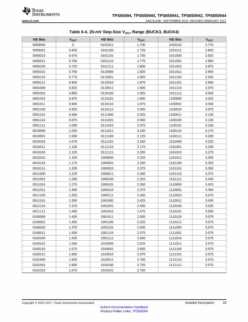
33
TPS65094, TPS650940, TPS650941, TPS650942, TPS650944www.ti.com SWCS133B –SEPTEMBER 2015–REVISED FEBRUARY 2017
Submit Documentation FeedbackProduct Folder Links: TPS65094
Detailed DescriptionCopyright © 2015–2017, Texas Instruments Incorporated
Table 6-4. 25-mV Step-Size VOUT Range (BUCK3, BUCK4)
VID Bits VOUT VID Bits VOUT VID Bits VOUT
0000000 0 0101011 1.700 1010110 2.7750000001 0.650 0101100 1.725 1010111 2.8000000010 0.675 0101101 1.750 1011000 2.8250000011 0.700 0101110 1.775 1011001 2.8500000100 0.725 0101111 1.800 1011010 2.8750000101 0.750 0110000 1.825 1011011 2.9000000110 0.775 0110001 1.850 1011100 2.9250000111 0.800 0110010 1.875 1011101 2.9500001000 0.825 0110011 1.900 1011110 2.9750001001 0.850 0110100 1.925 1011111 3.0000001010 0.875 0110101 1.950 1100000 3.0250001011 0.900 0110110 1.975 1100001 3.0500001100 0.925 0110111 2.000 1100010 3.0750001101 0.950 0111000 2.025 1100011 3.1000001110 0.975 0111001 2.050 1100100 3.1250001111 1.000 0111010 2.075 1100101 3.1500010000 1.025 0111011 2.100 1100110 3.1750010001 1.050 0111100 2.125 1100111 3.2000010010 1.075 0111101 2.150 1101000 3.2250010011 1.100 0111110 2.175 1101001 3.2500010100 1.125 0111111 2.200 1101010 3.2750010101 1.150 1000000 2.225 1101011 3.3000010110 1.175 1000001 2.250 1101100 3.3250010111 1.200 1000010 2.275 1101101 3.3500011000 1.225 1000011 2.300 1101110 3.3750011001 1.250 1000100 2.325 1101111 3.4000011010 1.275 1000101 2.350 1110000 3.4250011011 1.300 1000110 2.375 1110001 3.4500011100 1.325 1000111 2.400 1110010 3.4750011101 1.350 1001000 2.425 1110011 3.5000011110 1.375 1001001 2.450 1110100 3.5250011111 1.400 1001010 2.475 1110101 3.5500100000 1.425 1001011 2.500 1110110 3.5750100001 1.450 1001100 2.525 1110111 3.5750100010 1.475 1001101 2.550 1111000 3.5750100011 1.500 1001110 2.575 1111001 3.5750100100 1.525 1001111 2.600 1111010 3.5750100101 1.550 1010000 2.625 1111011 3.5750100110 1.575 1010001 2.650 1111100 3.5750100111 1.600 1010010 2.675 1111101 3.5750101000 1.625 1010011 2.700 1111110 3.5750101001 1.650 1010100 2.725 1111111 3.5750101010 1.675 1010101 2.750
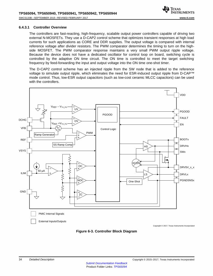
PGOOD
DCHG
SWx
NOC
ZC
XCON
DRVLx
PWMControl Logic
+
+
VREF +VTH_PG
+
+
UV
OV
+
VSYS
GND
REF
One-Shot
50 µA
BOOTx
DRVHx
FAULT
PGOOD
ILIM
+
VFB
OC+
+
SS Ramp Comp
EN
VDD
HS
LS
DRV5V_x_x
PGNDSNSx
VREF ± VTH_PG
++
Ramp Generator
PMIC Internal Signals
External Inputs/Outputs
Copyright © 2017, Texas Instruments Incorporated
34
TPS65094, TPS650940, TPS650941, TPS650942, TPS650944SWCS133B –SEPTEMBER 2015–REVISED FEBRUARY 2017 www.ti.com
Submit Documentation FeedbackProduct Folder Links: TPS65094
Detailed Description Copyright © 2015–2017, Texas Instruments Incorporated
6.4.3.1 Controller Overview
The controllers are fast-reacting, high-frequency, scalable output power controllers capable of driving twoexternal N-MOSFETs. They use a D-CAP2 control scheme that optimizes transient responses at high loadcurrents for such applications as CORE and DDR supplies. The output voltage is compared with internalreference voltage after divider resistors. The PWM comparator determines the timing to turn on the high-side MOSFET. The PWM comparator response maintains a very small PWM output ripple voltage.Because the device does not have a dedicated oscillator for control loop on board, switching cycle iscontrolled by the adaptive ON time circuit. The ON time is controlled to meet the target switchingfrequency by feed-forwarding the input and output voltage into the ON time one-shot timer.
The D-CAP2 control scheme has an injected ripple from the SW node that is added to the referencevoltage to simulate output ripple, which eliminates the need for ESR-induced output ripple from D-CAP™mode control. Thus, low-ESR output capacitors (such as low-cost ceramic MLCC capacitors) can be usedwith the controllers.
Figure 6-3. Controller Block Diagram
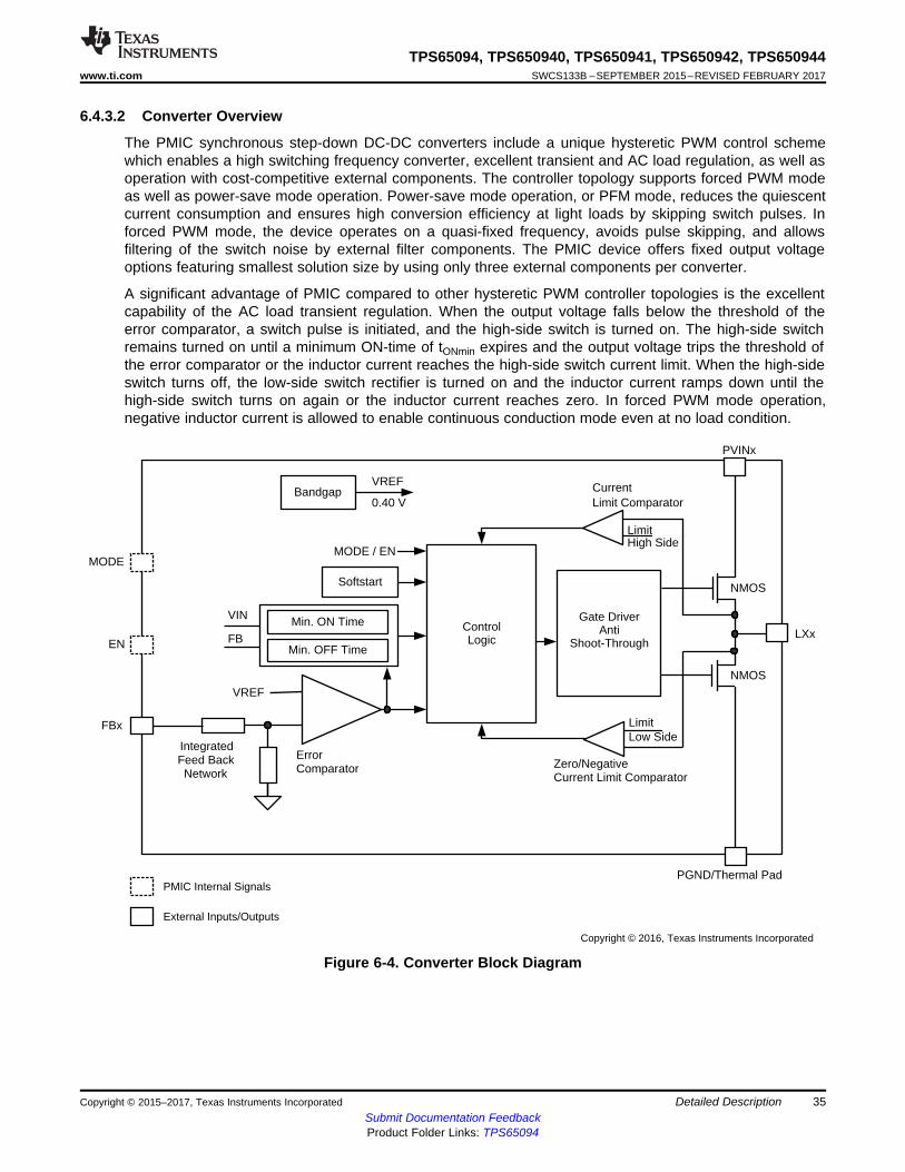
Bandgap
Min. ON Time
Min. OFF Time
Gate DriverAnti
Shoot-Through
Current Limit Comparator
LXx
LimitHigh Side
LimitLow Side
FBx
EN
MODE
PVINx
PGND/Thermal Pad
VIN
IntegratedFeed BackNetwork
VREF
FB
ErrorComparator Zero/Negative
Current Limit Comparator
ControlLogic
NMOS
NMOS
MODE / EN
VREF
0.40 V
Softstart
PMIC Internal Signals
External Inputs/Outputs
Copyright © 2016, Texas Instruments Incorporated
35
TPS65094, TPS650940, TPS650941, TPS650942, TPS650944www.ti.com SWCS133B –SEPTEMBER 2015–REVISED FEBRUARY 2017
Submit Documentation FeedbackProduct Folder Links: TPS65094
Detailed DescriptionCopyright © 2015–2017, Texas Instruments Incorporated
6.4.3.2 Converter Overview
The PMIC synchronous step-down DC-DC converters include a unique hysteretic PWM control schemewhich enables a high switching frequency converter, excellent transient and AC load regulation, as well asoperation with cost-competitive external components. The controller topology supports forced PWM modeas well as power-save mode operation. Power-save mode operation, or PFM mode, reduces the quiescentcurrent consumption and ensures high conversion efficiency at light loads by skipping switch pulses. Inforced PWM mode, the device operates on a quasi-fixed frequency, avoids pulse skipping, and allowsfiltering of the switch noise by external filter components. The PMIC device offers fixed output voltageoptions featuring smallest solution size by using only three external components per converter.
A significant advantage of PMIC compared to other hysteretic PWM controller topologies is the excellentcapability of the AC load transient regulation. When the output voltage falls below the threshold of theerror comparator, a switch pulse is initiated, and the high-side switch is turned on. The high-side switchremains turned on until a minimum ON-time of tONmin expires and the output voltage trips the threshold ofthe error comparator or the inductor current reaches the high-side switch current limit. When the high-sideswitch turns off, the low-side switch rectifier is turned on and the inductor current ramps down until thehigh-side switch turns on again or the inductor current reaches zero. In forced PWM mode operation,negative inductor current is allowed to enable continuous conduction mode even at no load condition.
Figure 6-4. Converter Block Diagram
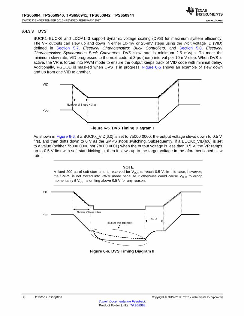
VID
Number of Steps × 3 µsVOUT
200 µs
load and time dependent
VID
Number of Steps × 3 µs
VOUT
36
TPS65094, TPS650940, TPS650941, TPS650942, TPS650944SWCS133B –SEPTEMBER 2015–REVISED FEBRUARY 2017 www.ti.com
Submit Documentation FeedbackProduct Folder Links: TPS65094
Detailed Description Copyright © 2015–2017, Texas Instruments Incorporated
6.4.3.3 DVS
BUCK1–BUCK6 and LDOA1–3 support dynamic voltage scaling (DVS) for maximum system efficiency.The VR outputs can slew up and down in either 10-mV or 25-mV steps using the 7-bit voltage ID (VID)defined in Section 5.7, Electrical Characteristics: Buck Controllers, and Section 5.8, ElectricalCharacteristics: Synchronous Buck Converters. DVS slew rate is minimum 2.5 mV/µs. To meet theminimum slew rate, VID progresses to the next code at 3-µs (nom) interval per 10-mV step. When DVS isactive, the VR is forced into PWM mode to ensure the output keeps track of VID code with minimal delay.Additionally, PGOOD is masked when DVS is in progress. Figure 6-5 shows an example of slew downand up from one VID to another.
Figure 6-5. DVS Timing Diagram I
As shown in Figure 6-6, if a BUCKx_VID[6:0] is set to 7b000 0000, the output voltage slews down to 0.5 Vfirst, and then drifts down to 0 V as the SMPS stops switching. Subsequently, if a BUCKx_VID[6:0] is setto a value (neither 7b000 0000 nor 7b000 0001) when the output voltage is less than 0.5 V, the VR rampsup to 0.5 V first with soft-start kicking in, then it slews up to the target voltage in the aforementioned slewrate.
NOTEA fixed 200 µs of soft-start time is reserved for VOUT to reach 0.5 V. In this case, however,the SMPS is not forced into PWM mode because it otherwise could cause VOUT to droopmomentarily if VOUT is drifting above 0.5 V for any reason.
Figure 6-6. DVS Timing Diagram II
OUT IN(MIN) OUTripple(min)
max IN(MIN) sw(max)
V (V V )I
L V f
-
=
´ ´
ripple(min)DSON LIM
ILIMLIMREF
IR 8 1.3 I
2R
I
æ ö´ ´ ´ -ç ÷
è ø=
37
TPS65094, TPS650940, TPS650941, TPS650942, TPS650944www.ti.com SWCS133B –SEPTEMBER 2015–REVISED FEBRUARY 2017
Submit Documentation FeedbackProduct Folder Links: TPS65094
Detailed DescriptionCopyright © 2015–2017, Texas Instruments Incorporated
6.4.3.4 Current Limit
The buck controllers (BUCK1, BUCK2, and BUCK6) have inductor-valley current-limit architecture and thecurrent limit is programmable by an external resistor at the ILIMx pin. Equation 1 shows the calculation fora desired resistor value, depending on specific application conditions. ILIMREF is the current source out ofthe ILIMx pin that is typically 50 µA, and RDSON is the maximum channel resistance of the low-side FET.The scaling factor is 1.3 to take into account all errors and temperature variations of RDSON, ILIMREF, andRILIM. Finally, 8 is another scaling factor associated with ILIMREF.
where• ILIM is the target current limit. An appropriate margin must be allowed when determining ILIM from
maximum output DC load current.• Iripple(min) is the minimum peak-to-peak inductor ripple current for a given VOUT. (1)
where• Lmax is maximum inductance• fsw(max) is maximum switching frequency• VIN(MIN) minimum input voltage to the external power stage (2)
The buck converter limit inductor peak current cycle-by-cycle to IIND_LIM is specified in Section 5.8,Electrical Characteristics: Synchronous Buck Converters.
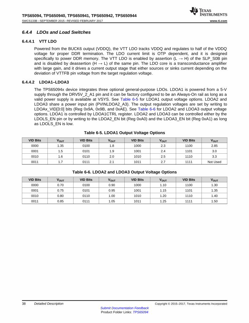
38
TPS65094, TPS650940, TPS650941, TPS650942, TPS650944SWCS133B –SEPTEMBER 2015–REVISED FEBRUARY 2017 www.ti.com
Submit Documentation FeedbackProduct Folder Links: TPS65094
Detailed Description Copyright © 2015–2017, Texas Instruments Incorporated
6.4.4 LDOs and Load Switches
6.4.4.1 VTT LDO
Powered from the BUCK6 output (VDDQ), the VTT LDO tracks VDDQ and regulates to half of the VDDQvoltage for proper DDR termination. The LDO current limit is OTP dependent, and it is designedspecifically to power DDR memory. The VTT LDO is enabled by assertion (L → H) of the SLP_S0B pinand is disabled by deassertion (H → L) of the same pin. The LDO core is a transconductance amplifierwith large gain, and it drives a current output stage that either sources or sinks current depending on thedeviation of VTTFB pin voltage from the target regulation voltage.
6.4.4.2 LDOA1–LDOA3
The TPS65094x device integrates three optional general-purpose LDOs. LDOA1 is powered from a 5-Vsupply through the DRV5V_2_A1 pin and it can be factory configured to be an Always-On rail as long as avalid power supply is available at VSYS. See Table 6-5 for LDOA1 output voltage options. LDOA2 andLDOA3 share a power input pin (PVINLDOA2_A3). The output regulation voltages are set by writing toLDOAx_VID[3:0] bits (Reg 0x9A, 0x9B, and 0xAE). See Table 6-6 for LDOA2 and LDOA3 output voltageoptions. LDOA1 is controlled by LDOA1CTRL register. LDOA2 and LDOA3 can be controlled either by theLDOLS_EN pin or by writing to the LDOA2_EN bit (Reg 0xA0) and the LDOA3_EN bit (Reg 0xA1) as longas LDOLS_EN is low.
Table 6-5. LDOA1 Output Voltage Options
VID Bits VOUT VID Bits VOUT VID Bits VOUT VID Bits VOUT
0000 1.35 0100 1.8 1000 2.3 1100 2.850001 1.5 0101 1.9 1001 2.4 1101 3.00010 1.6 0110 2.0 1010 2.5 1110 3.30011 1.7 0111 2.1 1011 2.7 1111 Not Used
Table 6-6. LDOA2 and LDOA3 Output Voltage Options
VID Bits VOUT VID Bits VOUT VID Bits VOUT VID Bits VOUT
0000 0.70 0100 0.90 1000 1.10 1100 1.300001 0.75 0101 0.95 1001 1.15 1101 1.350010 0.80 0110 1.00 1010 1.20 1110 1.400011 0.85 0111 1.05 1011 1.25 1111 1.50
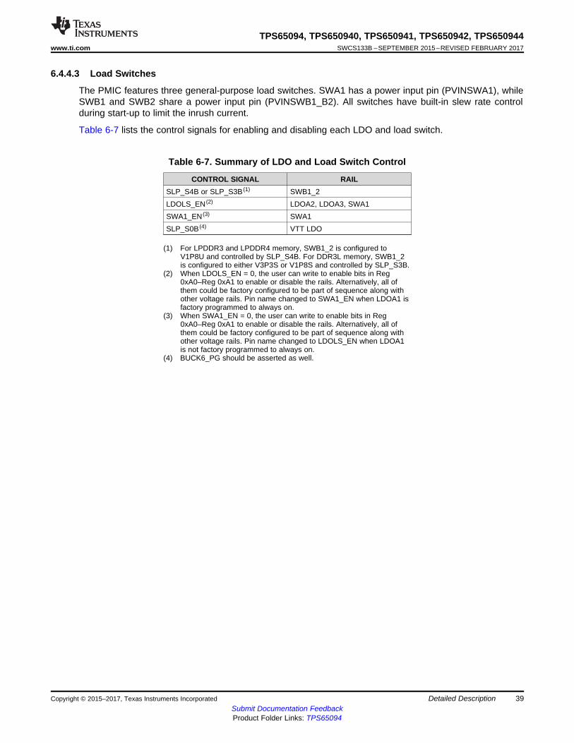
39
TPS65094, TPS650940, TPS650941, TPS650942, TPS650944www.ti.com SWCS133B –SEPTEMBER 2015–REVISED FEBRUARY 2017
Submit Documentation FeedbackProduct Folder Links: TPS65094
Detailed DescriptionCopyright © 2015–2017, Texas Instruments Incorporated
6.4.4.3 Load Switches
The PMIC features three general-purpose load switches. SWA1 has a power input pin (PVINSWA1), whileSWB1 and SWB2 share a power input pin (PVINSWB1_B2). All switches have built-in slew rate controlduring start-up to limit the inrush current.
Table 6-7 lists the control signals for enabling and disabling each LDO and load switch.
(1) For LPDDR3 and LPDDR4 memory, SWB1_2 is configured toV1P8U and controlled by SLP_S4B. For DDR3L memory, SWB1_2is configured to either V3P3S or V1P8S and controlled by SLP_S3B.
(2) When LDOLS_EN = 0, the user can write to enable bits in Reg0xA0–Reg 0xA1 to enable or disable the rails. Alternatively, all ofthem could be factory configured to be part of sequence along withother voltage rails. Pin name changed to SWA1_EN when LDOA1 isfactory programmed to always on.
(3) When SWA1_EN = 0, the user can write to enable bits in Reg0xA0–Reg 0xA1 to enable or disable the rails. Alternatively, all ofthem could be factory configured to be part of sequence along withother voltage rails. Pin name changed to LDOLS_EN when LDOA1is not factory programmed to always on.
(4) BUCK6_PG should be asserted as well.
Table 6-7. Summary of LDO and Load Switch Control
CONTROL SIGNAL RAILSLP_S4B or SLP_S3B (1) SWB1_2LDOLS_EN (2) LDOA2, LDOA3, SWA1SWA1_EN (3) SWA1SLP_S0B (4) VTT LDO
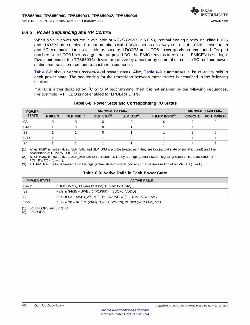
40
TPS65094, TPS650940, TPS650941, TPS650942, TPS650944SWCS133B –SEPTEMBER 2015–REVISED FEBRUARY 2017 www.ti.com
Submit Documentation FeedbackProduct Folder Links: TPS65094
Detailed Description Copyright © 2015–2017, Texas Instruments Incorporated
(1) When PMIC is first enabled, SLP_S4B and SLP_S3B are to be treated as if they are low (actual state of signal ignored) until thedeassertion of RSMRSTB (L → H).
(2) When PMIC is first enabled, SLP_S0B are to be treated as if they are high (actual state of signal ignored) until the assertion ofPCH_PWROK (L → H).
(3) THERMTRIPB is to be treated as if it is high (actual state of signal ignored) until the deassertion of RSMRSTB (L → H).
6.4.5 Power Sequencing and VR ControlWhen a valid power source is available at VSYS (VSYS ≥ 5.6 V), internal analog blocks including LDO5and LDO3P3 are enabled. For part numbers with LDOA1 set as an always on rail, the PMIC leaves resetand I2C communication is available as soon as LDO3P3 and LDO5 power goods are confirmed. For partnumbers with LDOA1 set as a general-purpose LDO, the PMIC remains in reset until PMICEN is set high.Five input pins of the TPS65094x device are driven by a host or by external-controller (EC) defined powerstates that transition from one to another in sequence.
Table 6-8 shows various system-level power states. Also, Table 6-9 summarizes a list of active rails ineach power state. The sequencing for the transitions between these states is described in the followingsections.
If a rail is either disabled by I2C or OTP programming, then it is not enabled by the following sequences.For example, VTT LDO is not enabled for LPDDR4 OTPs.
Table 6-8. Power State and Corresponding I/O Status
POWERSTATE
SIGNALS TO PMIC SIGNALS FROM PMICPMICEN SLP_S4B (1) SLP_S3B (1) SLP_S0B (2) THERMTRIPB (3) RSMRSTB PCH_PWROK
G3 0 0 0 0 0 0 0S4/S5 1 0 0 1 1 1 0S3 1 1 0 1 1 1 0S0iX 1 1 1 0 1 1 1S0 1 1 1 1 1 1 1
(1) For LPDDR3 and LPDDR4(2) For DDR3L
Table 6-9. Active Rails in Each Power State
POWER STATE ACTIVE RAILSS4/S5 BUCK1 (VNN), BUCK4 (V1P8A), BUCK5 (V1P24A)S3 Rails in S4/S5 + SWB1_2 (V1P8U) (1), BUCK6 (VDDQ)S0 Rails in S3 + SWB1_2 (2), VTT, BUCK2 (VCCGI), BUCK3 (VCCRAM)S0iX Rails in S0 – BUCK1 (VNN), BUCK2 (VCCGI), BUCK3 (VCCRAM), VTT
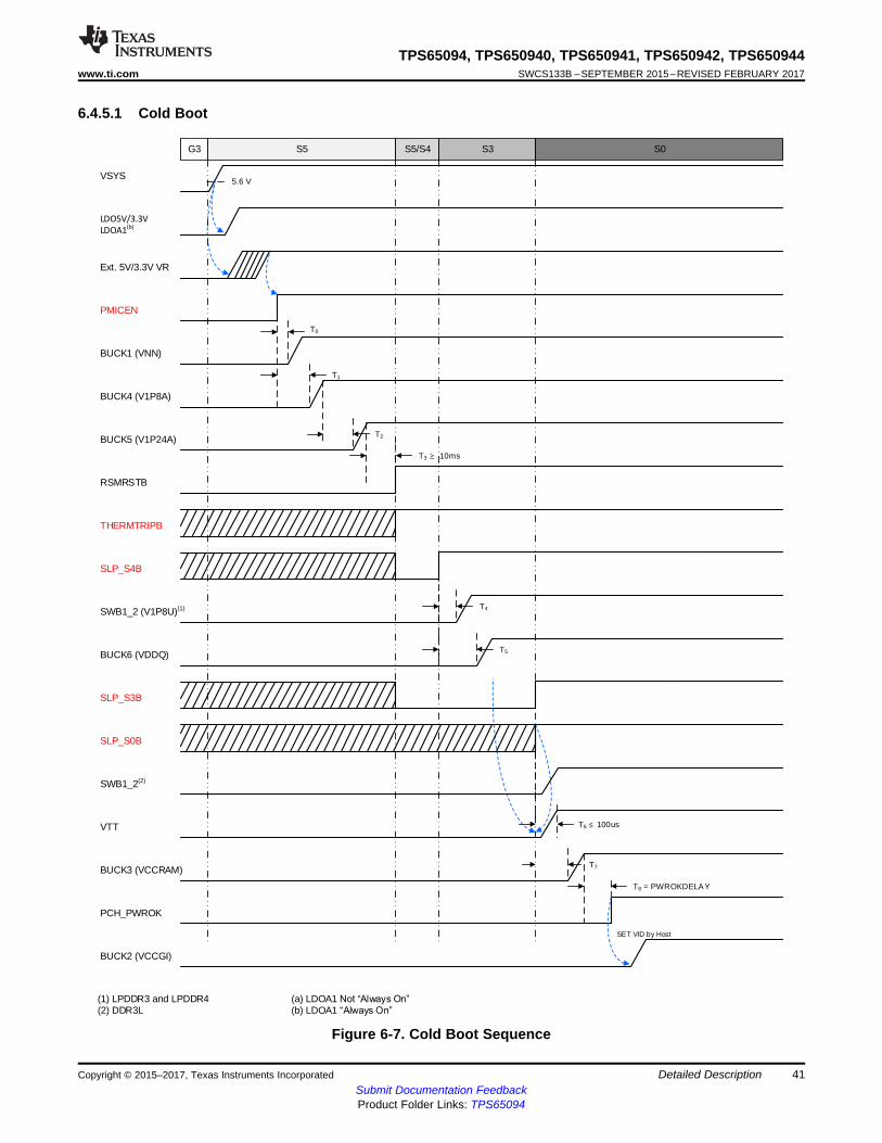
G3
VSYS
LDO5V/3.3V
LDOA1(b)
Ext. 5V/3.3V VR
PMICEN
BUCK1 (VNN)
BUCK4 (V1P8A)
T1
T2BUCK5 (V1P24A)
RSMRSTB
T3 � 10ms
SLP_S4B
SWB1_2 (V1P8U)(1) T4
T5BUCK6 (VDDQ)
VTT
SLP_S3B
BUCK3 (VCCRAM)
BUCK2 (VCCGI)
SLP_S0B
T6 � 100us
T7
PCH_PWROK
T8 = PWROKDELAY
S5 S5/S4 S3 S0
T0
5.6 V
THERMTRIPB
SET VID by Host
SWB1_2(2)
(a) LDOA1 1RW�³$OZD\V�2Q´(b) LDOA1 ³$OZD\V�2Q´
(1) LPDDR3 and LPDDR4(2) DDR3L
41
TPS65094, TPS650940, TPS650941, TPS650942, TPS650944www.ti.com SWCS133B –SEPTEMBER 2015–REVISED FEBRUARY 2017
Submit Documentation FeedbackProduct Folder Links: TPS65094
Detailed DescriptionCopyright © 2015–2017, Texas Instruments Incorporated
6.4.5.1 Cold Boot
Figure 6-7. Cold Boot Sequence
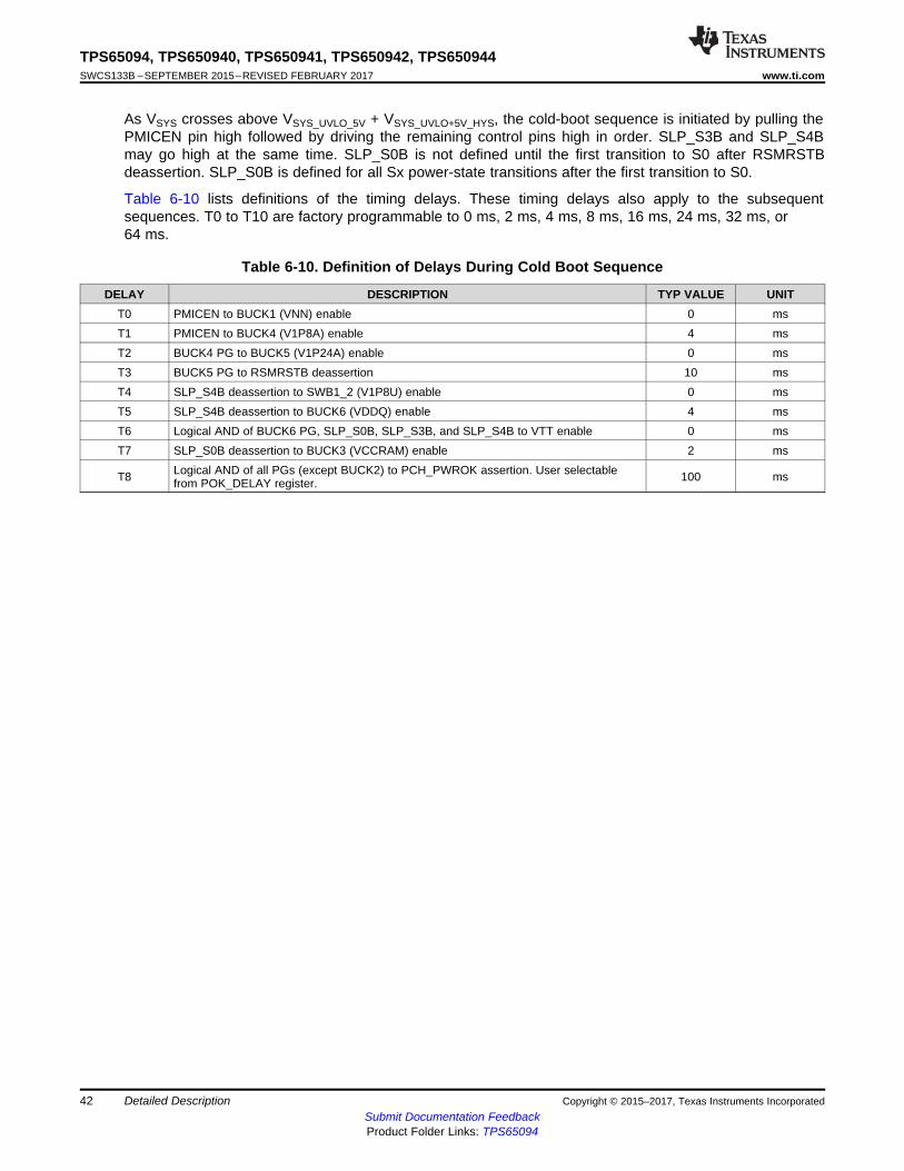
42
TPS65094, TPS650940, TPS650941, TPS650942, TPS650944SWCS133B –SEPTEMBER 2015–REVISED FEBRUARY 2017 www.ti.com
Submit Documentation FeedbackProduct Folder Links: TPS65094
Detailed Description Copyright © 2015–2017, Texas Instruments Incorporated
As VSYS crosses above VSYS_UVLO_5V + VSYS_UVLO+5V_HYS, the cold-boot sequence is initiated by pulling thePMICEN pin high followed by driving the remaining control pins high in order. SLP_S3B and SLP_S4Bmay go high at the same time. SLP_S0B is not defined until the first transition to S0 after RSMRSTBdeassertion. SLP_S0B is defined for all Sx power-state transitions after the first transition to S0.
Table 6-10 lists definitions of the timing delays. These timing delays also apply to the subsequentsequences. T0 to T10 are factory programmable to 0 ms, 2 ms, 4 ms, 8 ms, 16 ms, 24 ms, 32 ms, or64 ms.
Table 6-10. Definition of Delays During Cold Boot Sequence
DELAY DESCRIPTION TYP VALUE UNITT0 PMICEN to BUCK1 (VNN) enable 0 msT1 PMICEN to BUCK4 (V1P8A) enable 4 msT2 BUCK4 PG to BUCK5 (V1P24A) enable 0 msT3 BUCK5 PG to RSMRSTB deassertion 10 msT4 SLP_S4B deassertion to SWB1_2 (V1P8U) enable 0 msT5 SLP_S4B deassertion to BUCK6 (VDDQ) enable 4 msT6 Logical AND of BUCK6 PG, SLP_S0B, SLP_S3B, and SLP_S4B to VTT enable 0 msT7 SLP_S0B deassertion to BUCK3 (VCCRAM) enable 2 ms
T8 Logical AND of all PGs (except BUCK2) to PCH_PWROK assertion. User selectablefrom POK_DELAY register. 100 ms
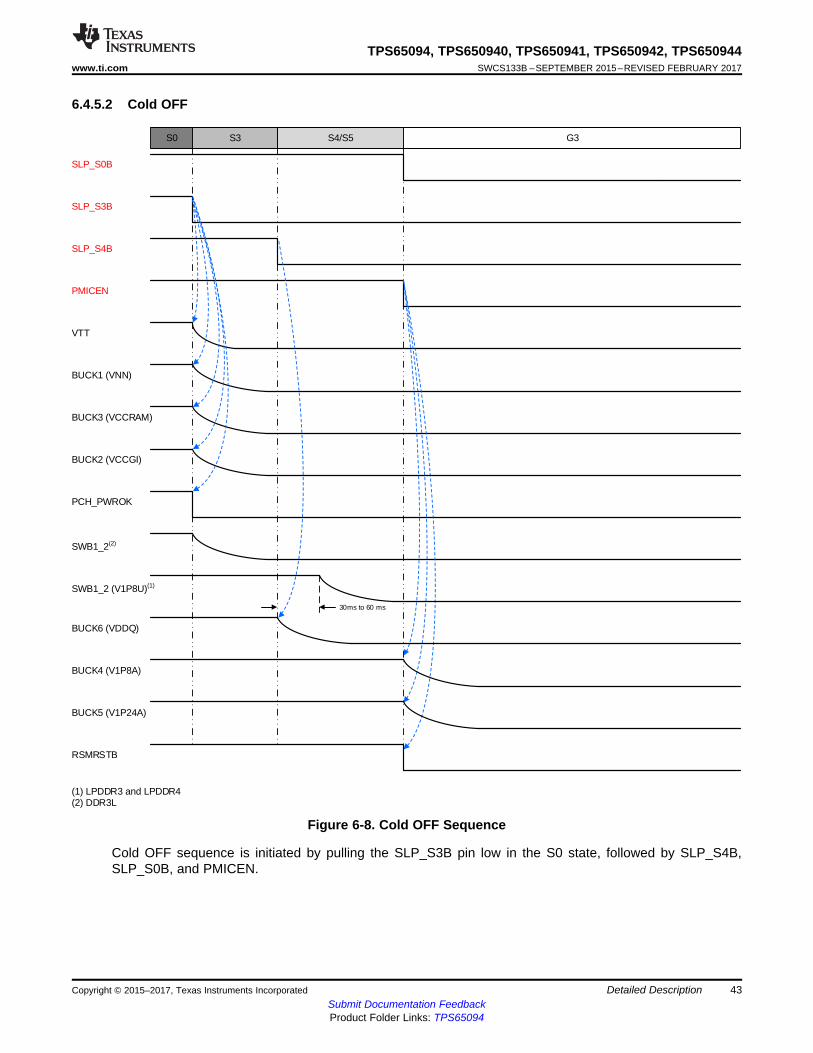
G3
SLP_S3B
VTT
SLP_S0B
PMICEN
SLP_S4B
SWB1_2(2)
PCH_PWROK
S4/S5S3S0
BUCK1 (VNN)
BUCK3 (VCCRAM)
BUCK2 (VCCGI)
BUCK4 (V1P8A)
BUCK5 (V1P24A)
RSMRSTB
SWB1_2 (V1P8U)(1)
BUCK6 (VDDQ)
30ms to 60 ms
(1) LPDDR3 and LPDDR4(2) DDR3L
43
TPS65094, TPS650940, TPS650941, TPS650942, TPS650944www.ti.com SWCS133B –SEPTEMBER 2015–REVISED FEBRUARY 2017
Submit Documentation FeedbackProduct Folder Links: TPS65094
Detailed DescriptionCopyright © 2015–2017, Texas Instruments Incorporated
6.4.5.2 Cold OFF
Figure 6-8. Cold OFF Sequence
Cold OFF sequence is initiated by pulling the SLP_S3B pin low in the S0 state, followed by SLP_S4B,SLP_S0B, and PMICEN.
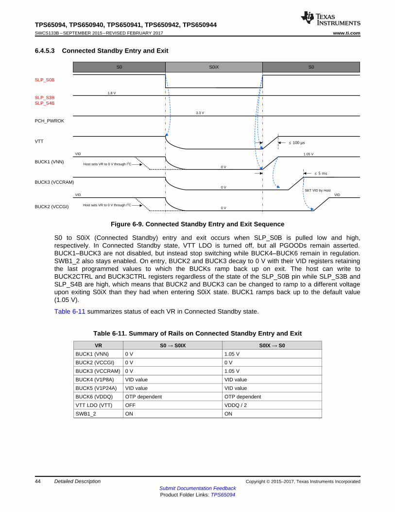
S0
SLP_S0B
VTT
BUCK1 (VNN)
PCH_PWROK
S0iXS0
BUCK2 (VCCGI)
BUCK3 (VCCRAM)
SLP_S3BSLP_S4B
3.3 V
1.8 V
1.05 V
0 V
0 V
Host sets VR to 0 V through I2C
Host sets VR to 0 V through I2C
0 V
� 100 µs
VID
VID VIDSET VID by Host
� 5 ms
44
TPS65094, TPS650940, TPS650941, TPS650942, TPS650944SWCS133B –SEPTEMBER 2015–REVISED FEBRUARY 2017 www.ti.com
Submit Documentation FeedbackProduct Folder Links: TPS65094
Detailed Description Copyright © 2015–2017, Texas Instruments Incorporated
6.4.5.3 Connected Standby Entry and Exit
Figure 6-9. Connected Standby Entry and Exit Sequence
S0 to S0iX (Connected Standby) entry and exit occurs when SLP_S0B is pulled low and high,respectively. In Connected Standby state, VTT LDO is turned off, but all PGOODs remain asserted.BUCK1–BUCK3 are not disabled, but instead stop switching while BUCK4–BUCK6 remain in regulation.SWB1_2 also stays enabled. On entry, BUCK2 and BUCK3 decay to 0 V with their VID registers retainingthe last programmed values to which the BUCKs ramp back up on exit. The host can write toBUCK2CTRL and BUCK3CTRL registers regardless of the state of the SLP_S0B pin while SLP_S3B andSLP_S4B are high, which means that BUCK2 and BUCK3 can be changed to ramp to a different voltageupon exiting S0iX than they had when entering S0iX state. BUCK1 ramps back up to the default value(1.05 V).
Table 6-11 summarizes status of each VR in Connected Standby state.
Table 6-11. Summary of Rails on Connected Standby Entry and Exit
VR S0 → S0IX S0IX → S0BUCK1 (VNN) 0 V 1.05 VBUCK2 (VCCGI) 0 V 0 VBUCK3 (VCCRAM) 0 V 1.05 VBUCK4 (V1P8A) VID value VID valueBUCK5 (V1P24A) VID value VID valueBUCK6 (VDDQ) OTP dependent OTP dependentVTT LDO (VTT) OFF VDDQ / 2SWB1_2 ON ON
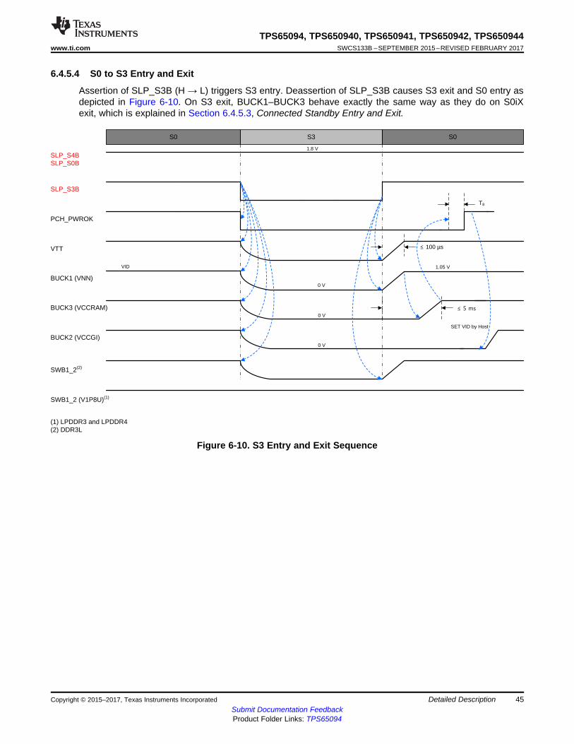
S0
SLP_S4BSLP_S0B
VTT
BUCK1 (VNN)
S0
BUCK2 (VCCGI)
BUCK3 (VCCRAM)
SLP_S3B
0 V
1.05 V
0 V
0 V
PCH_PWROK
S3
T8
1.8 V
VID
� 100 µs
� 5 ms
SET VID by Host
SWB1_2(2)
(1) LPDDR3 and LPDDR4(2) DDR3L
SWB1_2 (V1P8U)(1)
45
TPS65094, TPS650940, TPS650941, TPS650942, TPS650944www.ti.com SWCS133B –SEPTEMBER 2015–REVISED FEBRUARY 2017
Submit Documentation FeedbackProduct Folder Links: TPS65094
Detailed DescriptionCopyright © 2015–2017, Texas Instruments Incorporated
6.4.5.4 S0 to S3 Entry and Exit
Assertion of SLP_S3B (H → L) triggers S3 entry. Deassertion of SLP_S3B causes S3 exit and S0 entry asdepicted in Figure 6-10. On S3 exit, BUCK1–BUCK3 behave exactly the same way as they do on S0iXexit, which is explained in Section 6.4.5.3, Connected Standby Entry and Exit.
Figure 6-10. S3 Entry and Exit Sequence
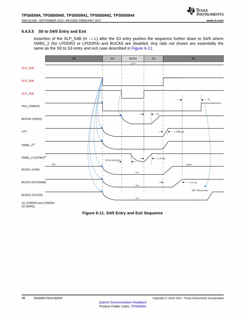
S0
SLP_S0B
VTT
BUCK1 (VNN)
S0
BUCK2 (VCCGI)
SLP_S3B
PCH_PWROK
S3
SWB1_2(2)
T8
S3S5/S4
SLP_S4B
BUCK6 (VDDQ)
T5
1.8 V
1.05 VVID
� 100 µs
0 V � 5 ms
0 V
SET VID by Host
BUCK3 (VCCRAM)
0 V
SWB1_2 (V1P8U)(1)� 2 ms
30 ms to 60 ms
(1) LPDDR3 and LPDDR4(2) DDR3L
46
TPS65094, TPS650940, TPS650941, TPS650942, TPS650944SWCS133B –SEPTEMBER 2015–REVISED FEBRUARY 2017 www.ti.com
Submit Documentation FeedbackProduct Folder Links: TPS65094
Detailed Description Copyright © 2015–2017, Texas Instruments Incorporated
6.4.5.5 S0 to S4/5 Entry and Exit
Assertion of the SLP_S4B (H → L) after the S3 entry pushes the sequence further down to S4/5 whereSWB1_2 (for LPDDR3 or LPDDR4) and BUCK6 are disabled. Any rails not shown are essentially thesame as the S0 to S3 entry and exit case described in Figure 6-11.
Figure 6-11. S4/5 Entry and Exit Sequence
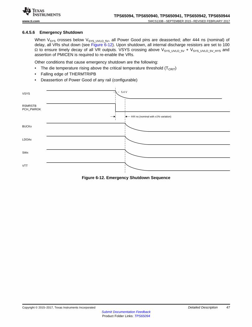
LDOAx
SWx
RSMRSTBPCH_PWROK
444 ns (nominal with ±1% variation)
VSYS
BUCKx
VTT
5.4 V
47
TPS65094, TPS650940, TPS650941, TPS650942, TPS650944www.ti.com SWCS133B –SEPTEMBER 2015–REVISED FEBRUARY 2017
Submit Documentation FeedbackProduct Folder Links: TPS65094
Detailed DescriptionCopyright © 2015–2017, Texas Instruments Incorporated
6.4.5.6 Emergency Shutdown
When VSYS crosses below VSYS_UVLO_5V, all Power Good pins are deasserted; after 444 ns (nominal) ofdelay, all VRs shut down (see Figure 6-12). Upon shutdown, all internal discharge resistors are set to 100Ω to ensure timely decay of all VR outputs. VSYS crossing above VSYS_UVLO_5V + VSYS_UVLO_5V_HYS andassertion of PMICEN is required to re-enable the VRs.
Other conditions that cause emergency shutdown are the following:• The die temperature rising above the critical temperature threshold (TCRIT)• Falling edge of THERMTRIPB• Deassertion of Power Good of any rail (configurable)
Figure 6-12. Emergency Shutdown Sequence
48
TPS65094, TPS650940, TPS650941, TPS650942, TPS650944SWCS133B –SEPTEMBER 2015–REVISED FEBRUARY 2017 www.ti.com
Submit Documentation FeedbackProduct Folder Links: TPS65094
Detailed Description Copyright © 2015–2017, Texas Instruments Incorporated
6.5 Device Functional Modes
6.5.1 Off ModeWhen power supply at the VSYS pin is less than VSYS_UVLO_5V (5.4-V nominal) + VSYS_UVLO_5V_HYS (0.2-Vnominal), the device is in off mode, where all output rails are disabled. If the supply voltage is greater thanVSYS_UVLO_3V (3.6-V nominal) + VSYS_UVLO_3V_HYS (0.15-V nominal) while it is still less than VSYS_UVLO_5V +VSYS_UVLO_5V_HYS, then the internal band-gap reference (VREF pin) along with LDO3P3 are enabled andregulated at target values.
6.5.2 Standby ModeWhen power supply at the VSYS pin rises above VSYS_UVLO_5V + VSYS_UVLO_5V_HYS, the device entersstandby mode, where all internal reference and regulators (LDO3P3 and LDO5) are running, and I2Cinterface and PMICEN pin are ready to respond. All default registers defined in Section 6.7, RegisterMaps, should now have been loaded from one-time programmable (OTP) memory. Quiescent currentconsumption in standby mode is specified in Section 5.5, Electrical Characteristics: Total CurrentConsumption.
6.5.3 Active ModeThe device proceeds to active mode when any output rail is enabled either through an input pin asdiscussed in Section 6.4.5, Power Sequencing and VR Control, or by writing to the EN bits through I2C.Output regulation voltage can also be changed by writing to the VID bits defined in Section 6.7, RegisterMaps.
6.6 I2C InterfaceThe I2C interface is a 2-wire serial interface developed by NXP™ (formerly Philips Semiconductor) (seethe I2C-Bus Specification and user manual, Rev 4, 13 February 2012). The bus consists of a data line(SDA) and a clock line (SCL) with pullup structures. When the bus is idle, both SDA and SCL lines arepulled high. All the I2C compatible devices connect to the I2C bus through open-drain I/O pins, DATA andCLK. A master device, usually a microcontroller or a digital signal processor, controls the bus. The masteris responsible for generating the SCL signal and device addresses. The master also generates specificconditions that indicate the start and stop of data transfer. A slave device receives and/or transmits dataon the bus under control of the master device.
The TPS65094x device works as a slave and supports the following data transfer modes, as defined in theI2C-Bus Specification: standard mode (100 kbps), fast mode (400 kbps), and high-speed mode(1 Mbps). The interface adds flexibility to the power supply solution, enabling programming of mostfunctions to new values depending on the instantaneous application requirements. Register contents areloaded when VSYS higher than VSYS_UVLO_5V is applied to the TPS65094x device. The I2C interface isrunning from an internal oscillator that is automatically enabled when there is an access to the interface.
The data transfer protocol for standard and fast modes are exactly the same, therefore, they are referredto as F/S-mode in this document. The protocol for high-speed mode is different from F/S-mode, and it isreferred to as H/S-mode.
The TPS65094x device supports 7-bit addressing; however, 10-bit addressing and general call addressare not supported. The default device address is 0x5E.
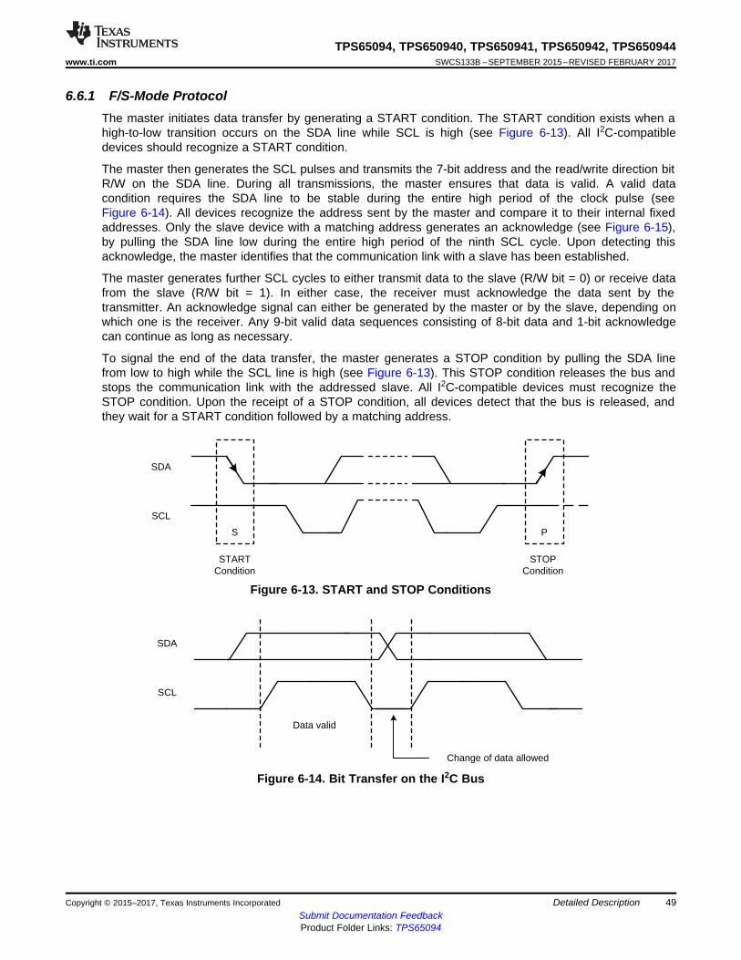
SDA
SCL
Data valid
Change of data allowed
SDA
SCL
S P
START Condition
STOPCondition
49
TPS65094, TPS650940, TPS650941, TPS650942, TPS650944www.ti.com SWCS133B –SEPTEMBER 2015–REVISED FEBRUARY 2017
Submit Documentation FeedbackProduct Folder Links: TPS65094
Detailed DescriptionCopyright © 2015–2017, Texas Instruments Incorporated
6.6.1 F/S-Mode ProtocolThe master initiates data transfer by generating a START condition. The START condition exists when ahigh-to-low transition occurs on the SDA line while SCL is high (see Figure 6-13). All I2C-compatibledevices should recognize a START condition.
The master then generates the SCL pulses and transmits the 7-bit address and the read/write direction bitR/W on the SDA line. During all transmissions, the master ensures that data is valid. A valid datacondition requires the SDA line to be stable during the entire high period of the clock pulse (seeFigure 6-14). All devices recognize the address sent by the master and compare it to their internal fixedaddresses. Only the slave device with a matching address generates an acknowledge (see Figure 6-15),by pulling the SDA line low during the entire high period of the ninth SCL cycle. Upon detecting thisacknowledge, the master identifies that the communication link with a slave has been established.
The master generates further SCL cycles to either transmit data to the slave (R/W bit = 0) or receive datafrom the slave (R/W bit = 1). In either case, the receiver must acknowledge the data sent by thetransmitter. An acknowledge signal can either be generated by the master or by the slave, depending onwhich one is the receiver. Any 9-bit valid data sequences consisting of 8-bit data and 1-bit acknowledgecan continue as long as necessary.
To signal the end of the data transfer, the master generates a STOP condition by pulling the SDA linefrom low to high while the SCL line is high (see Figure 6-13). This STOP condition releases the bus andstops the communication link with the addressed slave. All I2C-compatible devices must recognize theSTOP condition. Upon the receipt of a STOP condition, all devices detect that the bus is released, andthey wait for a START condition followed by a matching address.
Figure 6-13. START and STOP Conditions
Figure 6-14. Bit Transfer on the I2C Bus
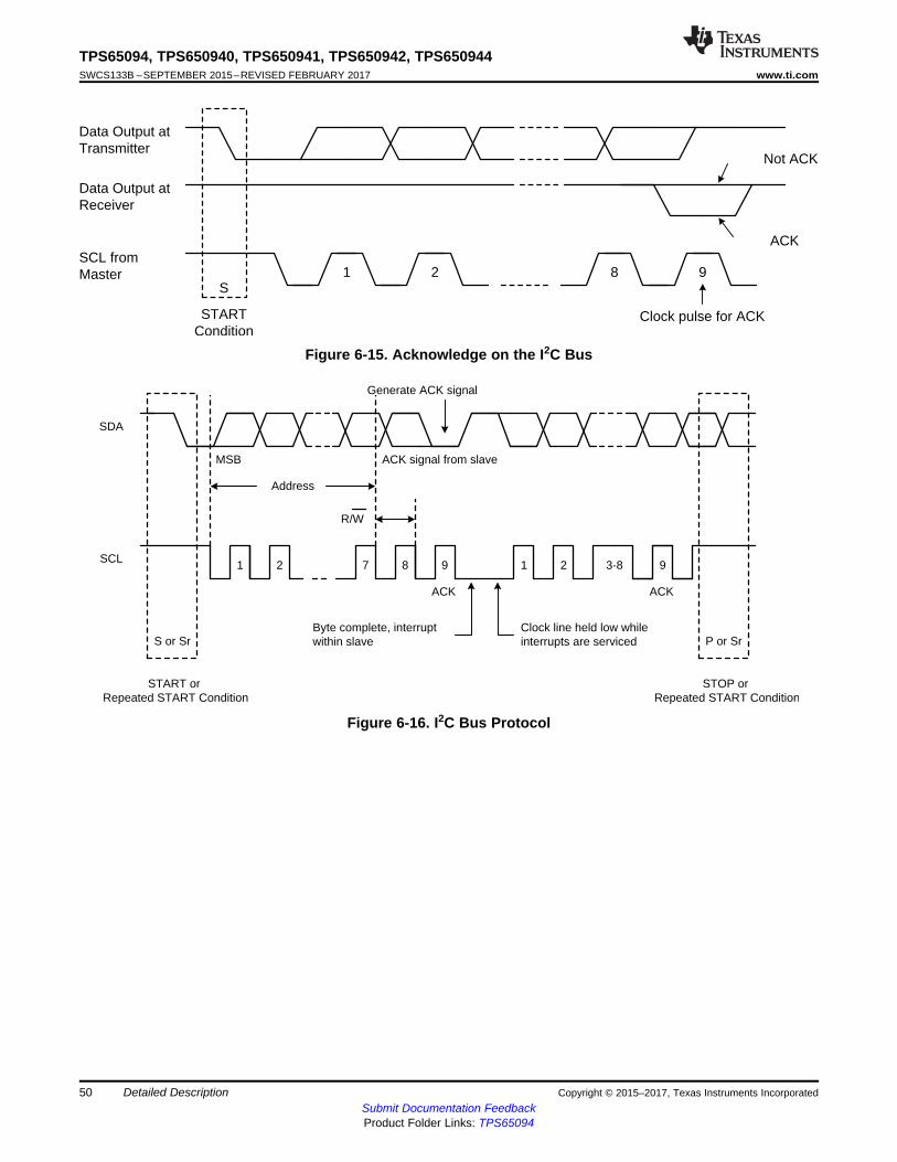
MSB
SDA
ACK signal from slave
Generate ACK signal
SCL 1 2 7 8 9 1 2 3-8 9
Address
R/W
ACK ACK
Byte complete, interrupt within slave
Clock line held low while interrupts are servicedS or Sr
START or Repeated START Condition
P or Sr
STOP or Repeated START Condition
Data Output at Transmitter
Data Output at Receiver
SCL from Master 1 2 8 9
S
START Condition
Not ACK
ACK
Clock pulse for ACK
50
TPS65094, TPS650940, TPS650941, TPS650942, TPS650944SWCS133B –SEPTEMBER 2015–REVISED FEBRUARY 2017 www.ti.com
Submit Documentation FeedbackProduct Folder Links: TPS65094
Detailed Description Copyright © 2015–2017, Texas Instruments Incorporated
Figure 6-15. Acknowledge on the I2C Bus
Figure 6-16. I2C Bus Protocol
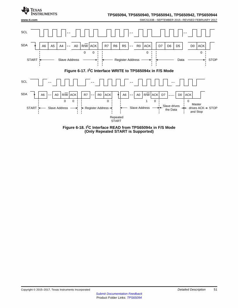
ACKA0 R7 R0 ACK A6 A0 ACK D7 D0 ACKA6
SCL
SDA
Slave Address Register Address Slave AddressSlave drives
the Data
Master drives ACK and Stop
STOPSTART
Repeated START
0 0 0 01
R/W R/W
0
A6 A5 A4 A0 ACK R7 R6 R5 R0 ACK D7 D6 D5 D0 ACK
SCL
SDA
Slave Address
0 0 0 0
Register Address DataSTART STOP
R/W
51
TPS65094, TPS650940, TPS650941, TPS650942, TPS650944www.ti.com SWCS133B –SEPTEMBER 2015–REVISED FEBRUARY 2017
Submit Documentation FeedbackProduct Folder Links: TPS65094
Detailed DescriptionCopyright © 2015–2017, Texas Instruments Incorporated
Figure 6-17. I2C Interface WRITE to TPS65094x in F/S Mode
Figure 6-18. I2C Interface READ from TPS65094x in F/S Mode(Only Repeated START is Supported)
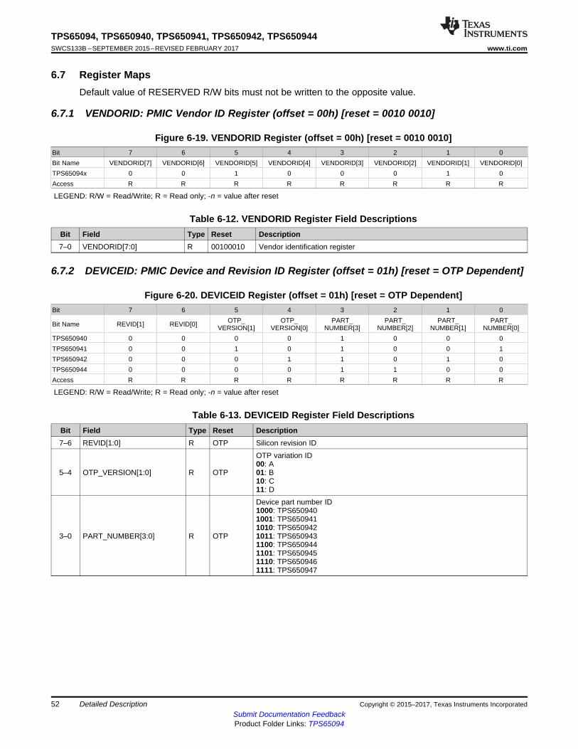
52
TPS65094, TPS650940, TPS650941, TPS650942, TPS650944SWCS133B –SEPTEMBER 2015–REVISED FEBRUARY 2017 www.ti.com
Submit Documentation FeedbackProduct Folder Links: TPS65094
Detailed Description Copyright © 2015–2017, Texas Instruments Incorporated
6.7 Register MapsDefault value of RESERVED R/W bits must not be written to the opposite value.
6.7.1 VENDORID: PMIC Vendor ID Register (offset = 00h) [reset = 0010 0010]
Figure 6-19. VENDORID Register (offset = 00h) [reset = 0010 0010]Bit 7 6 5 4 3 2 1 0Bit Name VENDORID[7] VENDORID[6] VENDORID[5] VENDORID[4] VENDORID[3] VENDORID[2] VENDORID[1] VENDORID[0]TPS65094x 0 0 1 0 0 0 1 0Access R R R R R R R R
LEGEND: R/W = Read/Write; R = Read only; -n = value after reset
Table 6-12. VENDORID Register Field DescriptionsBit Field Type Reset Description7–0 VENDORID[7:0] R 00100010 Vendor identification register
6.7.2 DEVICEID: PMIC Device and Revision ID Register (offset = 01h) [reset = OTP Dependent]
Figure 6-20. DEVICEID Register (offset = 01h) [reset = OTP Dependent]Bit 7 6 5 4 3 2 1 0
Bit Name REVID[1] REVID[0] OTP_VERSION[1]
OTP_VERSION[0]
PART_NUMBER[3]
PART_NUMBER[2]
PART_NUMBER[1]
PART_NUMBER[0]
TPS650940 0 0 0 0 1 0 0 0TPS650941 0 0 1 0 1 0 0 1TPS650942 0 0 0 1 1 0 1 0TPS650944 0 0 0 0 1 1 0 0Access R R R R R R R R
LEGEND: R/W = Read/Write; R = Read only; -n = value after reset
Table 6-13. DEVICEID Register Field DescriptionsBit Field Type Reset Description7–6 REVID[1:0] R OTP Silicon revision ID
5–4 OTP_VERSION[1:0] R OTP
OTP variation ID00: A01: B10: C11: D
3–0 PART_NUMBER[3:0] R OTP
Device part number ID1000: TPS6509401001: TPS6509411010: TPS6509421011: TPS6509431100: TPS6509441101: TPS6509451110: TPS6509461111: TPS650947
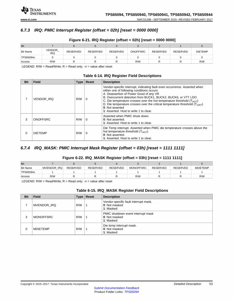
53
TPS65094, TPS650940, TPS650941, TPS650942, TPS650944www.ti.com SWCS133B –SEPTEMBER 2015–REVISED FEBRUARY 2017
Submit Documentation FeedbackProduct Folder Links: TPS65094
Detailed DescriptionCopyright © 2015–2017, Texas Instruments Incorporated
6.7.3 IRQ: PMIC Interrupt Register (offset = 02h) [reset = 0000 0000]
Figure 6-21. IRQ Register (offset = 02h) [reset = 0000 0000]Bit 7 6 5 4 3 2 1 0
Bit Name VENDOR_IRQ RESERVED RESERVED RESERVED ONOFFSRC RESERVED RESERVED DIETEMP
TPS65094x 0 0 0 0 0 0 0 0Access R/W R R R R/W R R R/W
LEGEND: R/W = Read/Write; R = Read only; -n = value after reset
Table 6-14. IRQ Register Field DescriptionsBit Field Type Reset Description
7 VENDOR_IRQ R/W 0
Vendor-specific interrupt, indicating fault even occurrence. Asserted wheneither one of following conditions occurs:A. Deassertion of Power Good of any VRB. Overcurrent detection from BUCK1, BUCK2, BUCK6, or VTT LDOC. Die temperature crosses over the hot temperature threshold (THOT)D. Die temperature crosses over the critical temperature threshold (TCRIT)0: Not asserted1: Asserted. Host to write 1 to clear.
3 ONOFFSRC R/W 0Asserted when PMIC shuts down.0: Not asserted.1: Asserted. Host to write 1 to clear.
0 DIETEMP R/W 0
Die Temp interrupt. Asserted when PMIC die temperature crosses above thehot temperature threshold (THOT).0: Not asserted.1: Asserted. Host to write 1 to clear.
6.7.4 IRQ_MASK: PMIC Interrupt Mask Register (offset = 03h) [reset = 1111 1111]
Figure 6-22. IRQ_MASK Register (offset = 03h) [reset = 1111 1111]Bit 7 6 5 4 3 2 1 0Bit Name MVENDOR_IRQ RESERVED RESERVED RESERVED MONOFFSRC RESERVED RESERVED MDIETEMPTPS65094x 1 1 1 1 1 1 1 1Access R/W R R R R/W R R R/W
LEGEND: R/W = Read/Write; R = Read only; -n = value after reset
Table 6-15. IRQ_MASK Register Field DescriptionsBit Field Type Reset Description
7 MVENDOR_IRQ R/W 1Vendor-specific fault interrupt mask.0: Not masked1: Masked
3 MONOFFSRC R/W 1PMIC shutdown event interrupt mask0: Not masked1: Masked
0 MDIETEMP R/W 1Die temp interrupt mask.0: Not masked1: Masked
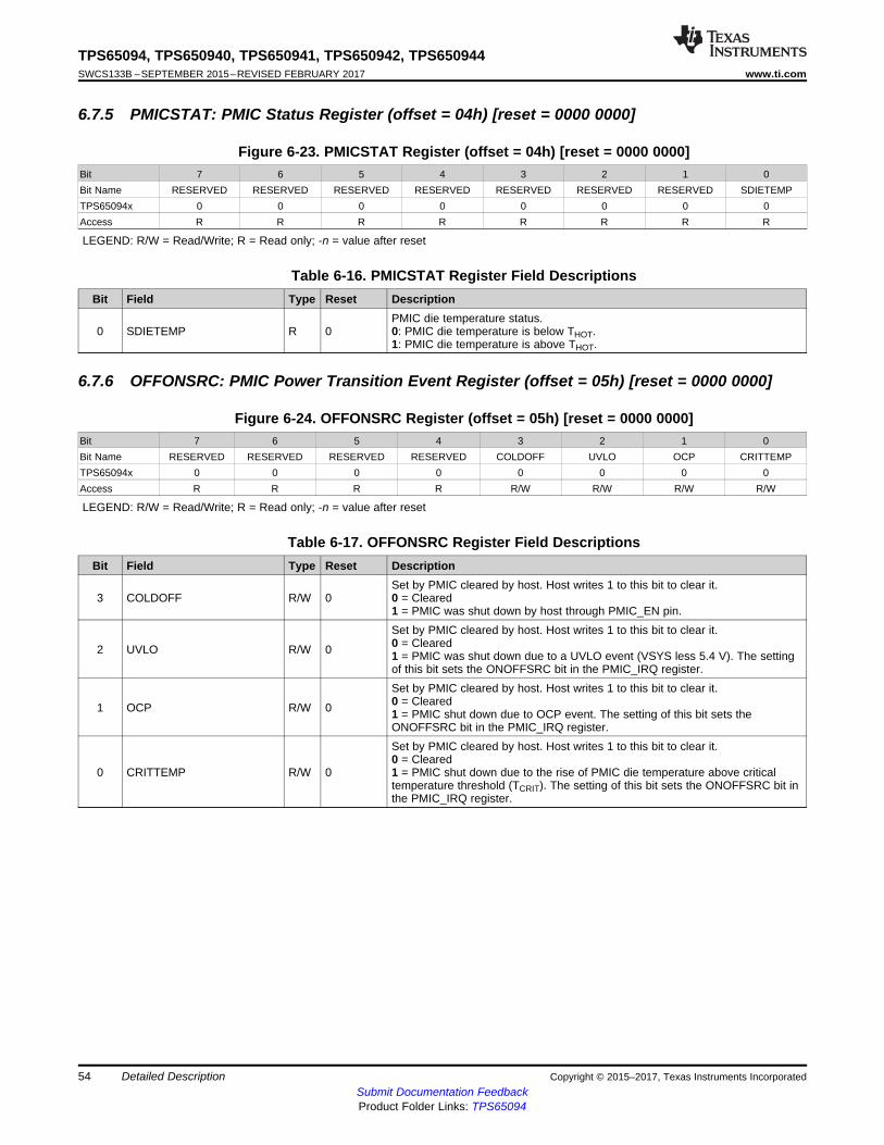
54
TPS65094, TPS650940, TPS650941, TPS650942, TPS650944SWCS133B –SEPTEMBER 2015–REVISED FEBRUARY 2017 www.ti.com
Submit Documentation FeedbackProduct Folder Links: TPS65094
Detailed Description Copyright © 2015–2017, Texas Instruments Incorporated
6.7.5 PMICSTAT: PMIC Status Register (offset = 04h) [reset = 0000 0000]
Figure 6-23. PMICSTAT Register (offset = 04h) [reset = 0000 0000]Bit 7 6 5 4 3 2 1 0Bit Name RESERVED RESERVED RESERVED RESERVED RESERVED RESERVED RESERVED SDIETEMPTPS65094x 0 0 0 0 0 0 0 0Access R R R R R R R R
LEGEND: R/W = Read/Write; R = Read only; -n = value after reset
Table 6-16. PMICSTAT Register Field DescriptionsBit Field Type Reset Description
0 SDIETEMP R 0PMIC die temperature status.0: PMIC die temperature is below THOT.1: PMIC die temperature is above THOT.
6.7.6 OFFONSRC: PMIC Power Transition Event Register (offset = 05h) [reset = 0000 0000]
Figure 6-24. OFFONSRC Register (offset = 05h) [reset = 0000 0000]Bit 7 6 5 4 3 2 1 0Bit Name RESERVED RESERVED RESERVED RESERVED COLDOFF UVLO OCP CRITTEMPTPS65094x 0 0 0 0 0 0 0 0Access R R R R R/W R/W R/W R/W
LEGEND: R/W = Read/Write; R = Read only; -n = value after reset
Table 6-17. OFFONSRC Register Field DescriptionsBit Field Type Reset Description
3 COLDOFF R/W 0Set by PMIC cleared by host. Host writes 1 to this bit to clear it.0 = Cleared1 = PMIC was shut down by host through PMIC_EN pin.
2 UVLO R/W 0
Set by PMIC cleared by host. Host writes 1 to this bit to clear it.0 = Cleared1 = PMIC was shut down due to a UVLO event (VSYS less 5.4 V). The settingof this bit sets the ONOFFSRC bit in the PMIC_IRQ register.
1 OCP R/W 0
Set by PMIC cleared by host. Host writes 1 to this bit to clear it.0 = Cleared1 = PMIC shut down due to OCP event. The setting of this bit sets theONOFFSRC bit in the PMIC_IRQ register.
0 CRITTEMP R/W 0
Set by PMIC cleared by host. Host writes 1 to this bit to clear it.0 = Cleared1 = PMIC shut down due to the rise of PMIC die temperature above criticaltemperature threshold (TCRIT). The setting of this bit sets the ONOFFSRC bit inthe PMIC_IRQ register.
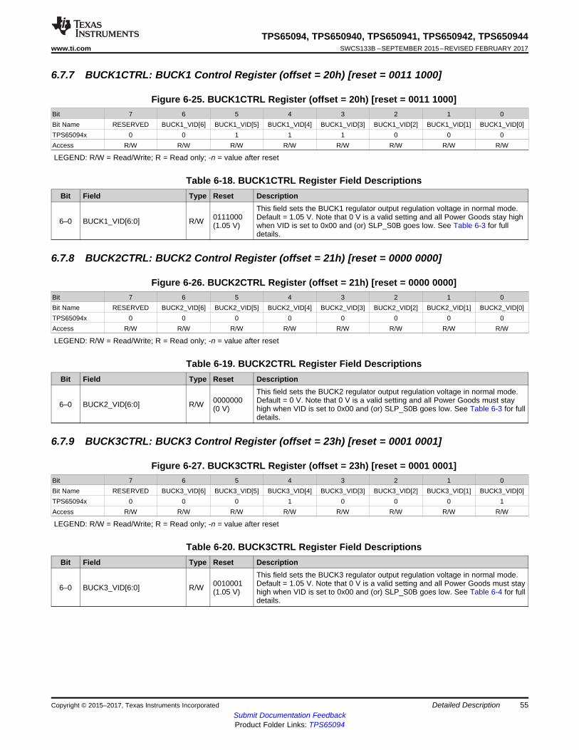
55
TPS65094, TPS650940, TPS650941, TPS650942, TPS650944www.ti.com SWCS133B –SEPTEMBER 2015–REVISED FEBRUARY 2017
Submit Documentation FeedbackProduct Folder Links: TPS65094
Detailed DescriptionCopyright © 2015–2017, Texas Instruments Incorporated
6.7.7 BUCK1CTRL: BUCK1 Control Register (offset = 20h) [reset = 0011 1000]
Figure 6-25. BUCK1CTRL Register (offset = 20h) [reset = 0011 1000]Bit 7 6 5 4 3 2 1 0Bit Name RESERVED BUCK1_VID[6] BUCK1_VID[5] BUCK1_VID[4] BUCK1_VID[3] BUCK1_VID[2] BUCK1_VID[1] BUCK1_VID[0]TPS65094x 0 0 1 1 1 0 0 0Access R/W R/W R/W R/W R/W R/W R/W R/W
LEGEND: R/W = Read/Write; R = Read only; -n = value after reset
Table 6-18. BUCK1CTRL Register Field DescriptionsBit Field Type Reset Description
6–0 BUCK1_VID[6:0] R/W 0111000(1.05 V)
This field sets the BUCK1 regulator output regulation voltage in normal mode.Default = 1.05 V. Note that 0 V is a valid setting and all Power Goods stay highwhen VID is set to 0x00 and (or) SLP_S0B goes low. See Table 6-3 for fulldetails.
6.7.8 BUCK2CTRL: BUCK2 Control Register (offset = 21h) [reset = 0000 0000]
Figure 6-26. BUCK2CTRL Register (offset = 21h) [reset = 0000 0000]Bit 7 6 5 4 3 2 1 0Bit Name RESERVED BUCK2_VID[6] BUCK2_VID[5] BUCK2_VID[4] BUCK2_VID[3] BUCK2_VID[2] BUCK2_VID[1] BUCK2_VID[0]TPS65094x 0 0 0 0 0 0 0 0Access R/W R/W R/W R/W R/W R/W R/W R/W
LEGEND: R/W = Read/Write; R = Read only; -n = value after reset
Table 6-19. BUCK2CTRL Register Field DescriptionsBit Field Type Reset Description
6–0 BUCK2_VID[6:0] R/W 0000000(0 V)
This field sets the BUCK2 regulator output regulation voltage in normal mode.Default = 0 V. Note that 0 V is a valid setting and all Power Goods must stayhigh when VID is set to 0x00 and (or) SLP_S0B goes low. See Table 6-3 for fulldetails.
6.7.9 BUCK3CTRL: BUCK3 Control Register (offset = 23h) [reset = 0001 0001]
Figure 6-27. BUCK3CTRL Register (offset = 23h) [reset = 0001 0001]Bit 7 6 5 4 3 2 1 0Bit Name RESERVED BUCK3_VID[6] BUCK3_VID[5] BUCK3_VID[4] BUCK3_VID[3] BUCK3_VID[2] BUCK3_VID[1] BUCK3_VID[0]TPS65094x 0 0 0 1 0 0 0 1Access R/W R/W R/W R/W R/W R/W R/W R/W
LEGEND: R/W = Read/Write; R = Read only; -n = value after reset
Table 6-20. BUCK3CTRL Register Field DescriptionsBit Field Type Reset Description
6–0 BUCK3_VID[6:0] R/W 0010001(1.05 V)
This field sets the BUCK3 regulator output regulation voltage in normal mode.Default = 1.05 V. Note that 0 V is a valid setting and all Power Goods must stayhigh when VID is set to 0x00 and (or) SLP_S0B goes low. See Table 6-4 for fulldetails.
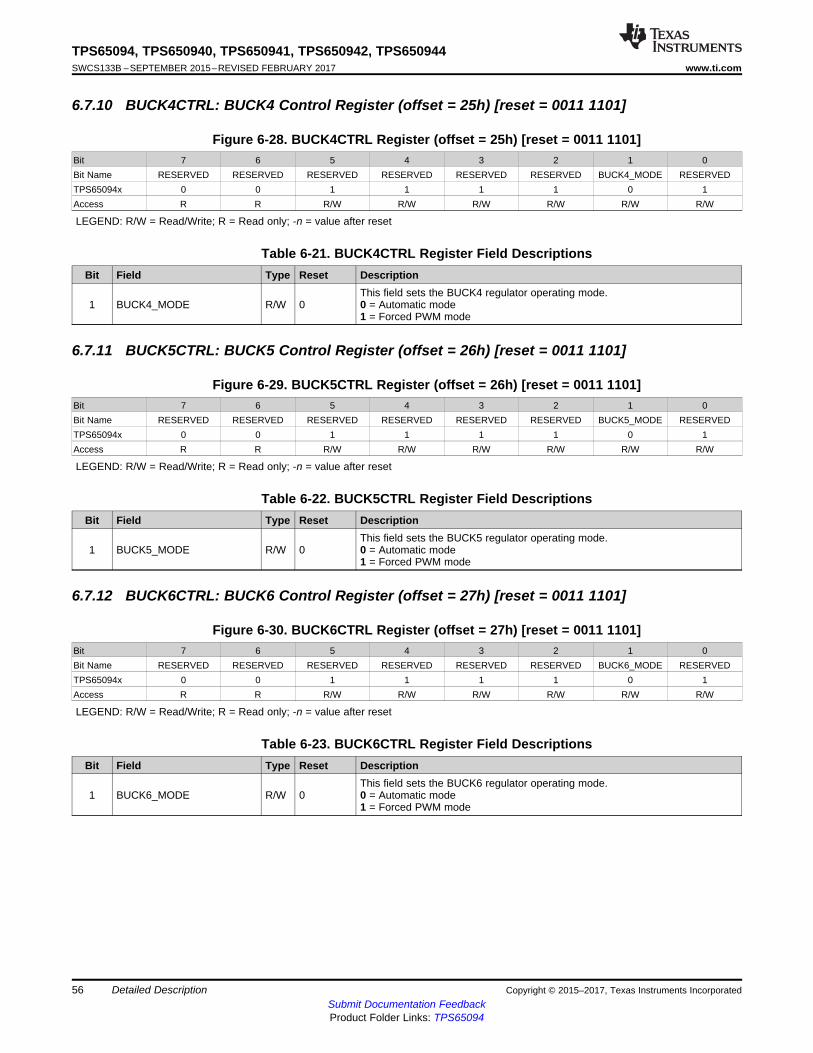
56
TPS65094, TPS650940, TPS650941, TPS650942, TPS650944SWCS133B –SEPTEMBER 2015–REVISED FEBRUARY 2017 www.ti.com
Submit Documentation FeedbackProduct Folder Links: TPS65094
Detailed Description Copyright © 2015–2017, Texas Instruments Incorporated
6.7.10 BUCK4CTRL: BUCK4 Control Register (offset = 25h) [reset = 0011 1101]
Figure 6-28. BUCK4CTRL Register (offset = 25h) [reset = 0011 1101]Bit 7 6 5 4 3 2 1 0Bit Name RESERVED RESERVED RESERVED RESERVED RESERVED RESERVED BUCK4_MODE RESERVEDTPS65094x 0 0 1 1 1 1 0 1Access R R R/W R/W R/W R/W R/W R/W
LEGEND: R/W = Read/Write; R = Read only; -n = value after reset
Table 6-21. BUCK4CTRL Register Field DescriptionsBit Field Type Reset Description
1 BUCK4_MODE R/W 0This field sets the BUCK4 regulator operating mode.0 = Automatic mode1 = Forced PWM mode
6.7.11 BUCK5CTRL: BUCK5 Control Register (offset = 26h) [reset = 0011 1101]
Figure 6-29. BUCK5CTRL Register (offset = 26h) [reset = 0011 1101]Bit 7 6 5 4 3 2 1 0Bit Name RESERVED RESERVED RESERVED RESERVED RESERVED RESERVED BUCK5_MODE RESERVEDTPS65094x 0 0 1 1 1 1 0 1Access R R R/W R/W R/W R/W R/W R/W
LEGEND: R/W = Read/Write; R = Read only; -n = value after reset
Table 6-22. BUCK5CTRL Register Field DescriptionsBit Field Type Reset Description
1 BUCK5_MODE R/W 0This field sets the BUCK5 regulator operating mode.0 = Automatic mode1 = Forced PWM mode
6.7.12 BUCK6CTRL: BUCK6 Control Register (offset = 27h) [reset = 0011 1101]
Figure 6-30. BUCK6CTRL Register (offset = 27h) [reset = 0011 1101]Bit 7 6 5 4 3 2 1 0Bit Name RESERVED RESERVED RESERVED RESERVED RESERVED RESERVED BUCK6_MODE RESERVEDTPS65094x 0 0 1 1 1 1 0 1Access R R R/W R/W R/W R/W R/W R/W
LEGEND: R/W = Read/Write; R = Read only; -n = value after reset
Table 6-23. BUCK6CTRL Register Field DescriptionsBit Field Type Reset Description
1 BUCK6_MODE R/W 0This field sets the BUCK6 regulator operating mode.0 = Automatic mode1 = Forced PWM mode
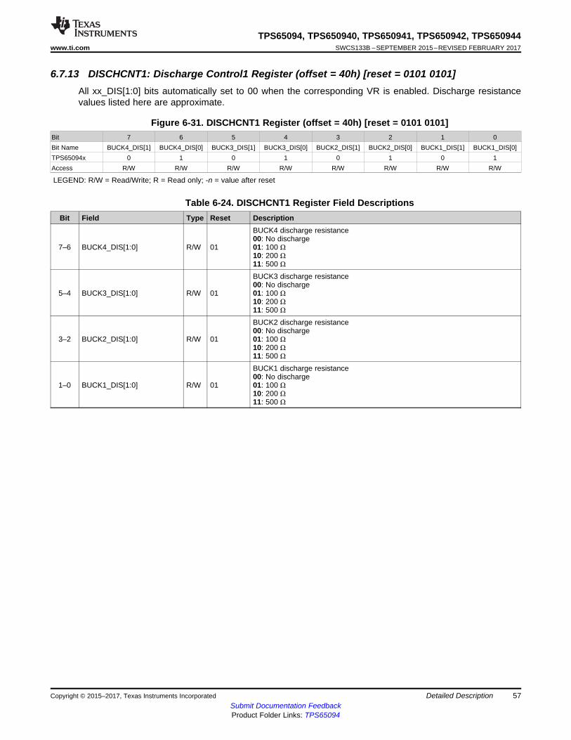
57
TPS65094, TPS650940, TPS650941, TPS650942, TPS650944www.ti.com SWCS133B –SEPTEMBER 2015–REVISED FEBRUARY 2017
Submit Documentation FeedbackProduct Folder Links: TPS65094
Detailed DescriptionCopyright © 2015–2017, Texas Instruments Incorporated
6.7.13 DISCHCNT1: Discharge Control1 Register (offset = 40h) [reset = 0101 0101]All xx_DIS[1:0] bits automatically set to 00 when the corresponding VR is enabled. Discharge resistancevalues listed here are approximate.
Figure 6-31. DISCHCNT1 Register (offset = 40h) [reset = 0101 0101]Bit 7 6 5 4 3 2 1 0Bit Name BUCK4_DIS[1] BUCK4_DIS[0] BUCK3_DIS[1] BUCK3_DIS[0] BUCK2_DIS[1] BUCK2_DIS[0] BUCK1_DIS[1] BUCK1_DIS[0]TPS65094x 0 1 0 1 0 1 0 1Access R/W R/W R/W R/W R/W R/W R/W R/W
LEGEND: R/W = Read/Write; R = Read only; -n = value after reset
Table 6-24. DISCHCNT1 Register Field DescriptionsBit Field Type Reset Description
7–6 BUCK4_DIS[1:0] R/W 01
BUCK4 discharge resistance00: No discharge01: 100 Ω10: 200 Ω11: 500 Ω
5–4 BUCK3_DIS[1:0] R/W 01
BUCK3 discharge resistance00: No discharge01: 100 Ω10: 200 Ω11: 500 Ω
3–2 BUCK2_DIS[1:0] R/W 01
BUCK2 discharge resistance00: No discharge01: 100 Ω10: 200 Ω11: 500 Ω
1–0 BUCK1_DIS[1:0] R/W 01
BUCK1 discharge resistance00: No discharge01: 100 Ω10: 200 Ω11: 500 Ω
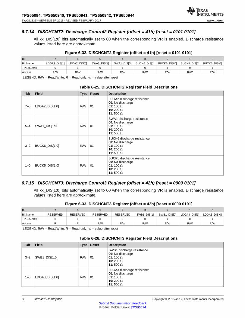
58
TPS65094, TPS650940, TPS650941, TPS650942, TPS650944SWCS133B –SEPTEMBER 2015–REVISED FEBRUARY 2017 www.ti.com
Submit Documentation FeedbackProduct Folder Links: TPS65094
Detailed Description Copyright © 2015–2017, Texas Instruments Incorporated
6.7.14 DISCHCNT2: Discharge Control2 Register (offset = 41h) [reset = 0101 0101]All xx_DIS[1:0] bits automatically set to 00 when the corresponding VR is enabled. Discharge resistancevalues listed here are approximate.
Figure 6-32. DISCHCNT2 Register (offset = 41h) [reset = 0101 0101]Bit 7 6 5 4 3 2 1 0Bit Name LDOA2_DIS[1] LDOA2_DIS[0] SWA1_DIS[1] SWA1_DIS[0] BUCK6_DIS[1] BUCK6_DIS[0] BUCK5_DIS[1] BUCK5_DIS[0]TPS65094x 0 1 0 1 0 1 0 1Access R/W R/W R/W R/W R/W R/W R/W R/W
LEGEND: R/W = Read/Write; R = Read only; -n = value after reset
Table 6-25. DISCHCNT2 Register Field DescriptionsBit Field Type Reset Description
7–6 LDOA2_DIS[1:0] R/W 01
LDOA2 discharge resistance00: No discharge01: 100 Ω10: 200 Ω11: 500 Ω
5–4 SWA1_DIS[1:0] R/W 01
SWA1 discharge resistance00: No discharge01: 100 Ω10: 200 Ω11: 500 Ω
3–2 BUCK6_DIS[1:0] R/W 01
BUCK6 discharge resistance00: No discharge01: 100 Ω10: 200 Ω11: 500 Ω
1–0 BUCK5_DIS[1:0] R/W 01
BUCK5 discharge resistance00: No discharge01: 100 Ω10: 200 Ω11: 500 Ω
6.7.15 DISCHCNT3: Discharge Control3 Register (offset = 42h) [reset = 0000 0101]All xx_DIS[1:0] bits automatically set to 00 when the corresponding VR is enabled. Discharge resistancevalues listed here are approximate.
Figure 6-33. DISCHCNT3 Register (offset = 42h) [reset = 0000 0101]Bit 7 6 5 4 3 2 1 0Bit Name RESERVED RESERVED RESERVED RESERVED SWB1_DIS[1] SWB1_DIS[0] LDOA3_DIS[1] LDOA3_DIS[0]TPS65094x 0 0 0 0 0 1 0 1Access R R R/W R/W R/W R/W R/W R/W
LEGEND: R/W = Read/Write; R = Read only; -n = value after reset
Table 6-26. DISCHCNT3 Register Field DescriptionsBit Field Type Reset Description
3–2 SWB1_DIS[1:0] R/W 01
SWB1 discharge resistance00: No discharge01: 100 Ω10: 200 Ω11: 500 Ω
1–0 LDOA3_DIS[1:0] R/W 01
LDOA3 discharge resistance00: No discharge01: 100 Ω10: 200 Ω11: 500 Ω
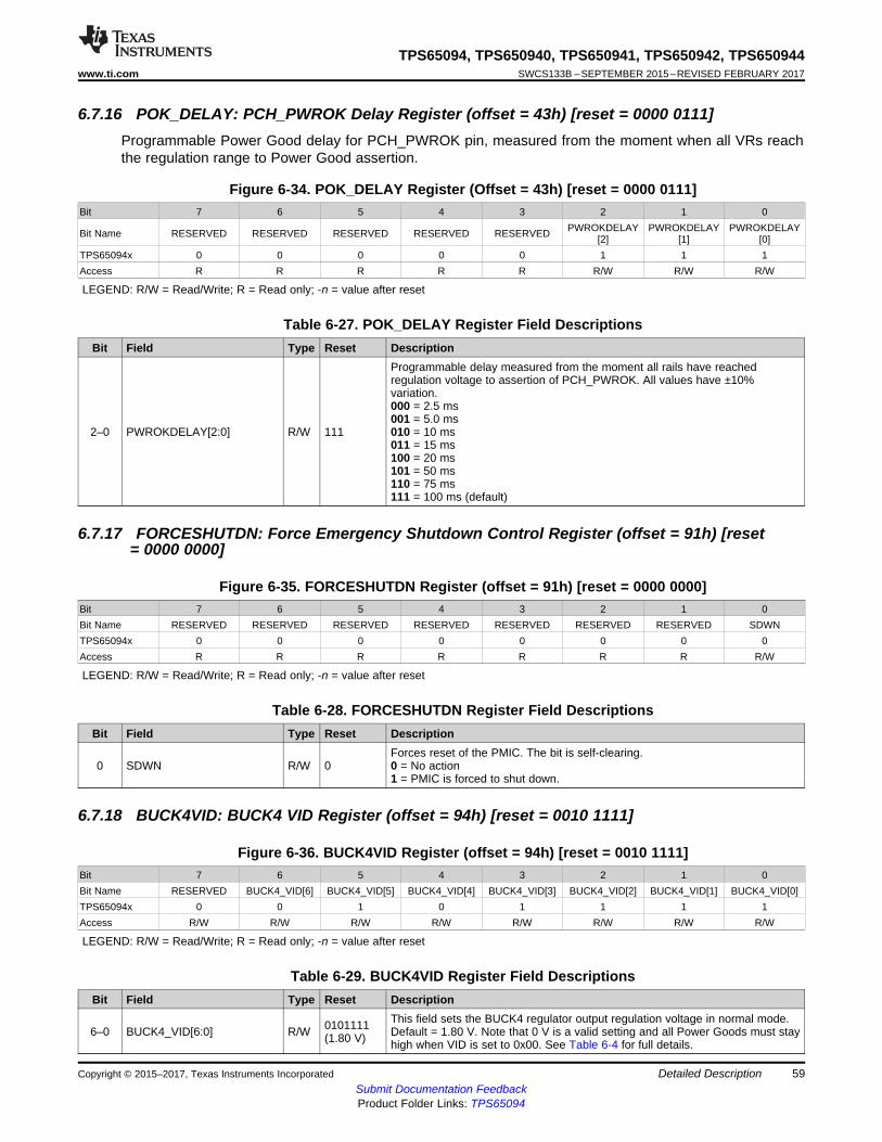
59
TPS65094, TPS650940, TPS650941, TPS650942, TPS650944www.ti.com SWCS133B –SEPTEMBER 2015–REVISED FEBRUARY 2017
Submit Documentation FeedbackProduct Folder Links: TPS65094
Detailed DescriptionCopyright © 2015–2017, Texas Instruments Incorporated
6.7.16 POK_DELAY: PCH_PWROK Delay Register (offset = 43h) [reset = 0000 0111]Programmable Power Good delay for PCH_PWROK pin, measured from the moment when all VRs reachthe regulation range to Power Good assertion.
Figure 6-34. POK_DELAY Register (Offset = 43h) [reset = 0000 0111]Bit 7 6 5 4 3 2 1 0
Bit Name RESERVED RESERVED RESERVED RESERVED RESERVED PWROKDELAY[2]
PWROKDELAY[1]
PWROKDELAY[0]
TPS65094x 0 0 0 0 0 1 1 1Access R R R R R R/W R/W R/W
LEGEND: R/W = Read/Write; R = Read only; -n = value after reset
Table 6-27. POK_DELAY Register Field DescriptionsBit Field Type Reset Description
2–0 PWROKDELAY[2:0] R/W 111
Programmable delay measured from the moment all rails have reachedregulation voltage to assertion of PCH_PWROK. All values have ±10%variation.000 = 2.5 ms001 = 5.0 ms010 = 10 ms011 = 15 ms100 = 20 ms101 = 50 ms110 = 75 ms111 = 100 ms (default)
6.7.17 FORCESHUTDN: Force Emergency Shutdown Control Register (offset = 91h) [reset= 0000 0000]
Figure 6-35. FORCESHUTDN Register (offset = 91h) [reset = 0000 0000]Bit 7 6 5 4 3 2 1 0Bit Name RESERVED RESERVED RESERVED RESERVED RESERVED RESERVED RESERVED SDWNTPS65094x 0 0 0 0 0 0 0 0Access R R R R R R R R/W
LEGEND: R/W = Read/Write; R = Read only; -n = value after reset
Table 6-28. FORCESHUTDN Register Field DescriptionsBit Field Type Reset Description
0 SDWN R/W 0Forces reset of the PMIC. The bit is self-clearing.0 = No action1 = PMIC is forced to shut down.
6.7.18 BUCK4VID: BUCK4 VID Register (offset = 94h) [reset = 0010 1111]
Figure 6-36. BUCK4VID Register (offset = 94h) [reset = 0010 1111]Bit 7 6 5 4 3 2 1 0Bit Name RESERVED BUCK4_VID[6] BUCK4_VID[5] BUCK4_VID[4] BUCK4_VID[3] BUCK4_VID[2] BUCK4_VID[1] BUCK4_VID[0]TPS65094x 0 0 1 0 1 1 1 1Access R/W R/W R/W R/W R/W R/W R/W R/W
LEGEND: R/W = Read/Write; R = Read only; -n = value after reset
Table 6-29. BUCK4VID Register Field DescriptionsBit Field Type Reset Description
6–0 BUCK4_VID[6:0] R/W 0101111(1.80 V)
This field sets the BUCK4 regulator output regulation voltage in normal mode.Default = 1.80 V. Note that 0 V is a valid setting and all Power Goods must stayhigh when VID is set to 0x00. See Table 6-4 for full details.
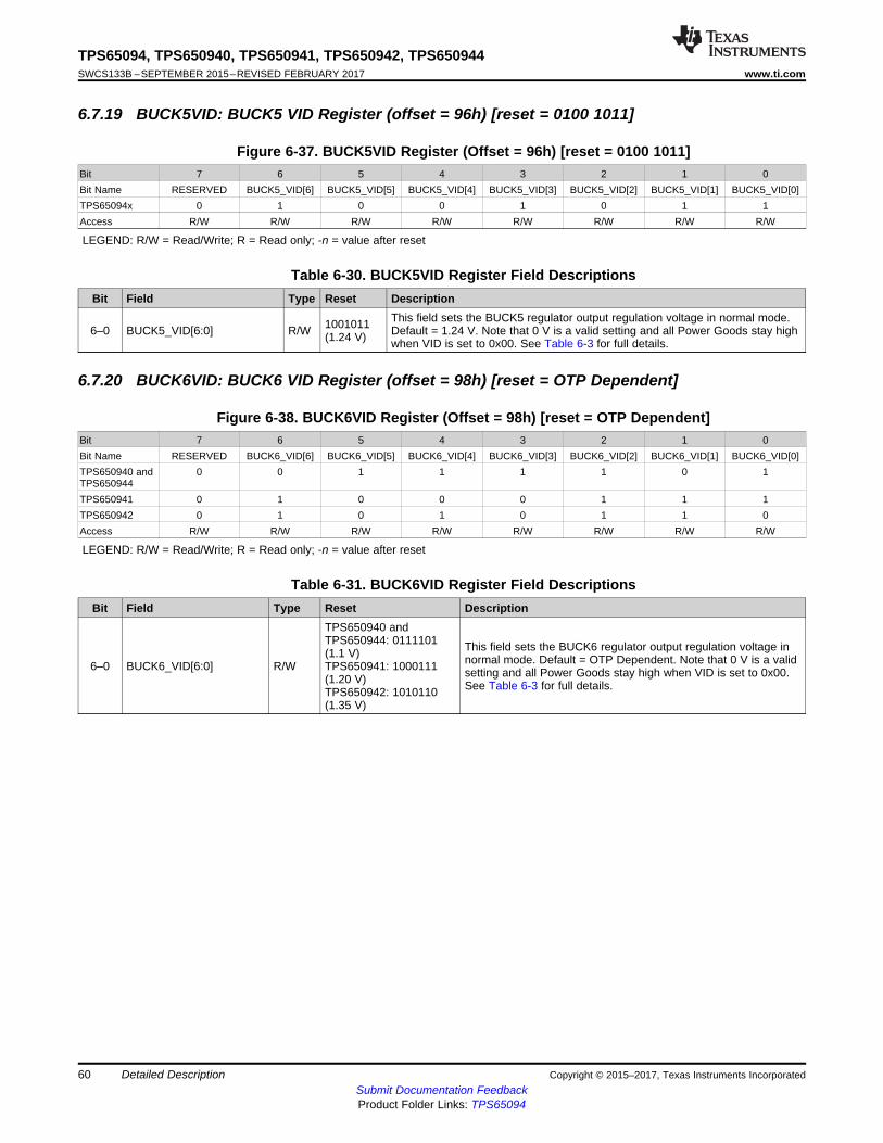
60
TPS65094, TPS650940, TPS650941, TPS650942, TPS650944SWCS133B –SEPTEMBER 2015–REVISED FEBRUARY 2017 www.ti.com
Submit Documentation FeedbackProduct Folder Links: TPS65094
Detailed Description Copyright © 2015–2017, Texas Instruments Incorporated
6.7.19 BUCK5VID: BUCK5 VID Register (offset = 96h) [reset = 0100 1011]
Figure 6-37. BUCK5VID Register (Offset = 96h) [reset = 0100 1011]Bit 7 6 5 4 3 2 1 0Bit Name RESERVED BUCK5_VID[6] BUCK5_VID[5] BUCK5_VID[4] BUCK5_VID[3] BUCK5_VID[2] BUCK5_VID[1] BUCK5_VID[0]TPS65094x 0 1 0 0 1 0 1 1Access R/W R/W R/W R/W R/W R/W R/W R/W
LEGEND: R/W = Read/Write; R = Read only; -n = value after reset
Table 6-30. BUCK5VID Register Field DescriptionsBit Field Type Reset Description
6–0 BUCK5_VID[6:0] R/W 1001011(1.24 V)
This field sets the BUCK5 regulator output regulation voltage in normal mode.Default = 1.24 V. Note that 0 V is a valid setting and all Power Goods stay highwhen VID is set to 0x00. See Table 6-3 for full details.
6.7.20 BUCK6VID: BUCK6 VID Register (offset = 98h) [reset = OTP Dependent]
Figure 6-38. BUCK6VID Register (Offset = 98h) [reset = OTP Dependent]Bit 7 6 5 4 3 2 1 0Bit Name RESERVED BUCK6_VID[6] BUCK6_VID[5] BUCK6_VID[4] BUCK6_VID[3] BUCK6_VID[2] BUCK6_VID[1] BUCK6_VID[0]TPS650940 andTPS650944
0 0 1 1 1 1 0 1
TPS650941 0 1 0 0 0 1 1 1TPS650942 0 1 0 1 0 1 1 0Access R/W R/W R/W R/W R/W R/W R/W R/W
LEGEND: R/W = Read/Write; R = Read only; -n = value after reset
Table 6-31. BUCK6VID Register Field DescriptionsBit Field Type Reset Description
6–0 BUCK6_VID[6:0] R/W
TPS650940 andTPS650944: 0111101(1.1 V)TPS650941: 1000111(1.20 V)TPS650942: 1010110(1.35 V)
This field sets the BUCK6 regulator output regulation voltage innormal mode. Default = OTP Dependent. Note that 0 V is a validsetting and all Power Goods stay high when VID is set to 0x00.See Table 6-3 for full details.
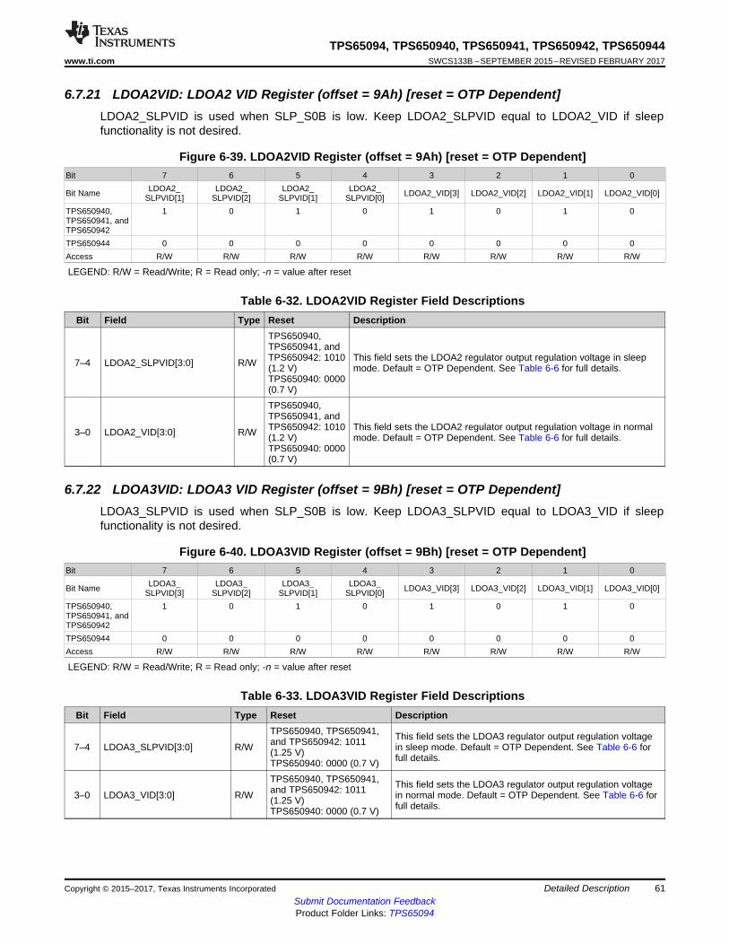
61
TPS65094, TPS650940, TPS650941, TPS650942, TPS650944www.ti.com SWCS133B –SEPTEMBER 2015–REVISED FEBRUARY 2017
Submit Documentation FeedbackProduct Folder Links: TPS65094
Detailed DescriptionCopyright © 2015–2017, Texas Instruments Incorporated
6.7.21 LDOA2VID: LDOA2 VID Register (offset = 9Ah) [reset = OTP Dependent]LDOA2_SLPVID is used when SLP_S0B is low. Keep LDOA2_SLPVID equal to LDOA2_VID if sleepfunctionality is not desired.
Figure 6-39. LDOA2VID Register (offset = 9Ah) [reset = OTP Dependent]Bit 7 6 5 4 3 2 1 0
Bit Name LDOA2_SLPVID[1]
LDOA2_SLPVID[2]
LDOA2_SLPVID[1]
LDOA2_SLPVID[0] LDOA2_VID[3] LDOA2_VID[2] LDOA2_VID[1] LDOA2_VID[0]
TPS650940,TPS650941, andTPS650942
1 0 1 0 1 0 1 0
TPS650944 0 0 0 0 0 0 0 0Access R/W R/W R/W R/W R/W R/W R/W R/W
LEGEND: R/W = Read/Write; R = Read only; -n = value after reset
Table 6-32. LDOA2VID Register Field DescriptionsBit Field Type Reset Description
7–4 LDOA2_SLPVID[3:0] R/W
TPS650940,TPS650941, andTPS650942: 1010(1.2 V)TPS650940: 0000(0.7 V)
This field sets the LDOA2 regulator output regulation voltage in sleepmode. Default = OTP Dependent. See Table 6-6 for full details.
3–0 LDOA2_VID[3:0] R/W
TPS650940,TPS650941, andTPS650942: 1010(1.2 V)TPS650940: 0000(0.7 V)
This field sets the LDOA2 regulator output regulation voltage in normalmode. Default = OTP Dependent. See Table 6-6 for full details.
6.7.22 LDOA3VID: LDOA3 VID Register (offset = 9Bh) [reset = OTP Dependent]LDOA3_SLPVID is used when SLP_S0B is low. Keep LDOA3_SLPVID equal to LDOA3_VID if sleepfunctionality is not desired.
Figure 6-40. LDOA3VID Register (offset = 9Bh) [reset = OTP Dependent]Bit 7 6 5 4 3 2 1 0
Bit Name LDOA3_SLPVID[3]
LDOA3_SLPVID[2]
LDOA3_SLPVID[1]
LDOA3_SLPVID[0] LDOA3_VID[3] LDOA3_VID[2] LDOA3_VID[1] LDOA3_VID[0]
TPS650940,TPS650941, andTPS650942
1 0 1 0 1 0 1 0
TPS650944 0 0 0 0 0 0 0 0Access R/W R/W R/W R/W R/W R/W R/W R/W
LEGEND: R/W = Read/Write; R = Read only; -n = value after reset
Table 6-33. LDOA3VID Register Field DescriptionsBit Field Type Reset Description
7–4 LDOA3_SLPVID[3:0] R/W
TPS650940, TPS650941,and TPS650942: 1011(1.25 V)TPS650940: 0000 (0.7 V)
This field sets the LDOA3 regulator output regulation voltagein sleep mode. Default = OTP Dependent. See Table 6-6 forfull details.
3–0 LDOA3_VID[3:0] R/W
TPS650940, TPS650941,and TPS650942: 1011(1.25 V)TPS650940: 0000 (0.7 V)
This field sets the LDOA3 regulator output regulation voltagein normal mode. Default = OTP Dependent. See Table 6-6 forfull details.
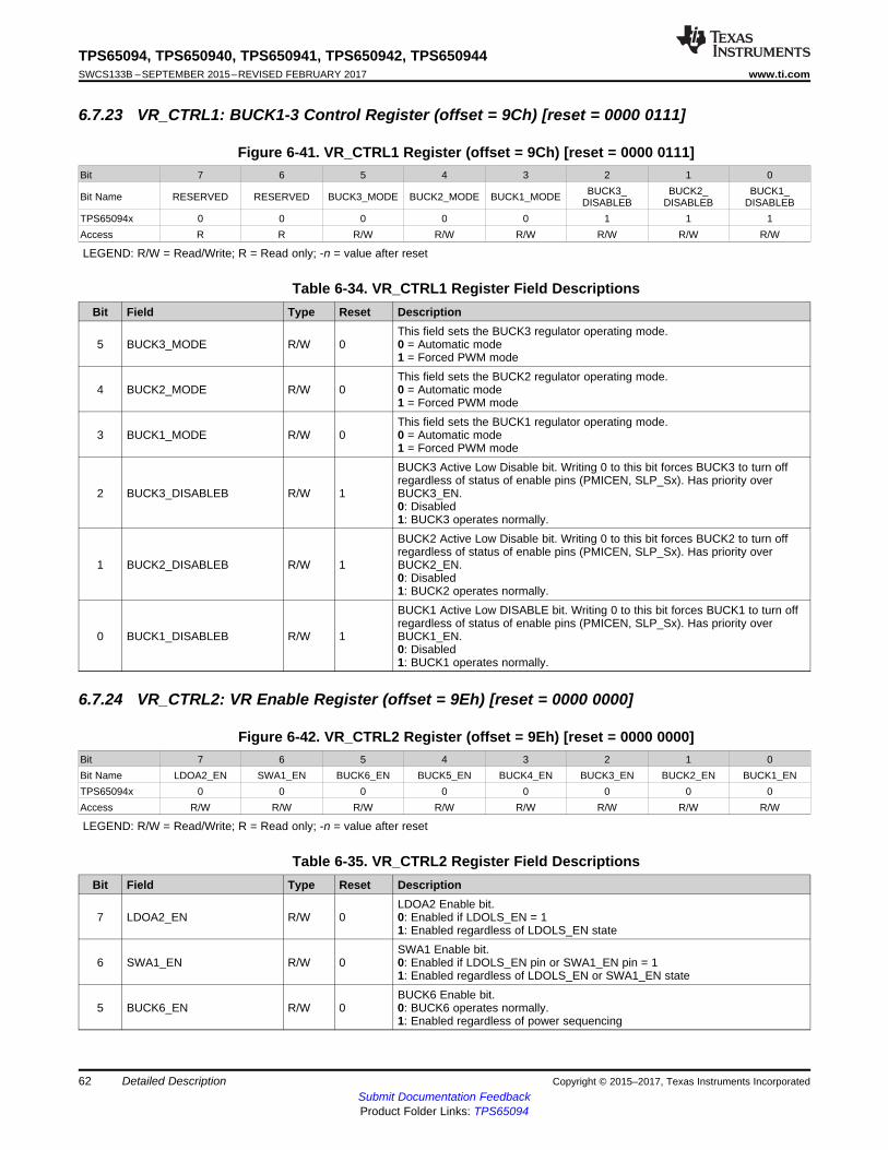
62
TPS65094, TPS650940, TPS650941, TPS650942, TPS650944SWCS133B –SEPTEMBER 2015–REVISED FEBRUARY 2017 www.ti.com
Submit Documentation FeedbackProduct Folder Links: TPS65094
Detailed Description Copyright © 2015–2017, Texas Instruments Incorporated
6.7.23 VR_CTRL1: BUCK1-3 Control Register (offset = 9Ch) [reset = 0000 0111]
Figure 6-41. VR_CTRL1 Register (offset = 9Ch) [reset = 0000 0111]Bit 7 6 5 4 3 2 1 0
Bit Name RESERVED RESERVED BUCK3_MODE BUCK2_MODE BUCK1_MODE BUCK3_DISABLEB
BUCK2_DISABLEB
BUCK1_DISABLEB
TPS65094x 0 0 0 0 0 1 1 1Access R R R/W R/W R/W R/W R/W R/W
LEGEND: R/W = Read/Write; R = Read only; -n = value after reset
Table 6-34. VR_CTRL1 Register Field DescriptionsBit Field Type Reset Description
5 BUCK3_MODE R/W 0This field sets the BUCK3 regulator operating mode.0 = Automatic mode1 = Forced PWM mode
4 BUCK2_MODE R/W 0This field sets the BUCK2 regulator operating mode.0 = Automatic mode1 = Forced PWM mode
3 BUCK1_MODE R/W 0This field sets the BUCK1 regulator operating mode.0 = Automatic mode1 = Forced PWM mode
2 BUCK3_DISABLEB R/W 1
BUCK3 Active Low Disable bit. Writing 0 to this bit forces BUCK3 to turn offregardless of status of enable pins (PMICEN, SLP_Sx). Has priority overBUCK3_EN.0: Disabled1: BUCK3 operates normally.
1 BUCK2_DISABLEB R/W 1
BUCK2 Active Low Disable bit. Writing 0 to this bit forces BUCK2 to turn offregardless of status of enable pins (PMICEN, SLP_Sx). Has priority overBUCK2_EN.0: Disabled1: BUCK2 operates normally.
0 BUCK1_DISABLEB R/W 1
BUCK1 Active Low DISABLE bit. Writing 0 to this bit forces BUCK1 to turn offregardless of status of enable pins (PMICEN, SLP_Sx). Has priority overBUCK1_EN.0: Disabled1: BUCK1 operates normally.
6.7.24 VR_CTRL2: VR Enable Register (offset = 9Eh) [reset = 0000 0000]
Figure 6-42. VR_CTRL2 Register (offset = 9Eh) [reset = 0000 0000]Bit 7 6 5 4 3 2 1 0Bit Name LDOA2_EN SWA1_EN BUCK6_EN BUCK5_EN BUCK4_EN BUCK3_EN BUCK2_EN BUCK1_ENTPS65094x 0 0 0 0 0 0 0 0Access R/W R/W R/W R/W R/W R/W R/W R/W
LEGEND: R/W = Read/Write; R = Read only; -n = value after reset
Table 6-35. VR_CTRL2 Register Field DescriptionsBit Field Type Reset Description
7 LDOA2_EN R/W 0LDOA2 Enable bit.0: Enabled if LDOLS_EN = 11: Enabled regardless of LDOLS_EN state
6 SWA1_EN R/W 0SWA1 Enable bit.0: Enabled if LDOLS_EN pin or SWA1_EN pin = 11: Enabled regardless of LDOLS_EN or SWA1_EN state
5 BUCK6_EN R/W 0BUCK6 Enable bit.0: BUCK6 operates normally.1: Enabled regardless of power sequencing
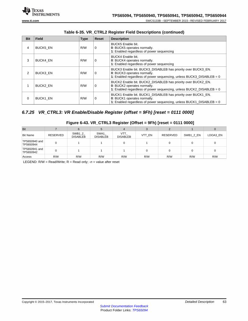
63
TPS65094, TPS650940, TPS650941, TPS650942, TPS650944www.ti.com SWCS133B –SEPTEMBER 2015–REVISED FEBRUARY 2017
Submit Documentation FeedbackProduct Folder Links: TPS65094
Detailed DescriptionCopyright © 2015–2017, Texas Instruments Incorporated
Table 6-35. VR_CTRL2 Register Field Descriptions (continued)Bit Field Type Reset Description
4 BUCK5_EN R/W 0BUCK5 Enable bit.0: BUCK5 operates normally.1: Enabled regardless of power sequencing
3 BUCK4_EN R/W 0BUCK4 Enable bit.0: BUCK4 operates normally.1: Enabled regardless of power sequencing
2 BUCK3_EN R/W 0BUCK3 Enable bit. BUCK3_DISABLEB has priority over BUCK3_EN.0: BUCK3 operates normally.1: Enabled regardless of power sequencing, unless BUCK3_DISABLEB = 0
1 BUCK2_EN R/W 0BUCK2 Enable bit. BUCK2_DISABLEB has priority over BUCK2_EN.0: BUCK2 operates normally.1: Enabled regardless of power sequencing, unless BUCK2_DISABLEB = 0
0 BUCK1_EN R/W 0BUCK1 Enable bit. BUCK1_DISABLEB has priority over BUCK1_EN.0: BUCK1 operates normally.1: Enabled regardless of power sequencing, unless BUCK1_DISABLEB = 0
6.7.25 VR_CTRL3: VR Enable/Disable Register (offset = 9Fh) [reset = 0111 0000]
Figure 6-43. VR_CTRL3 Register (Offset = 9Fh) [reset = 0111 0000]Bit 7 6 5 4 3 2 1 0
Bit Name RESERVED SWB1_2_DISABLEB
SWA1_DISABLEB
VTT_DISABLEB VTT_EN RESERVED SWB1_2_EN LDOA3_EN
TPS650940 andTPS650944 0 1 1 0 1 0 0 0
TPS650941 andTPS650942 0 1 1 1 0 0 0 0
Access R/W R/W R/W R/W R/W R/W R/W R/W
LEGEND: R/W = Read/Write; R = Read only; -n = value after reset
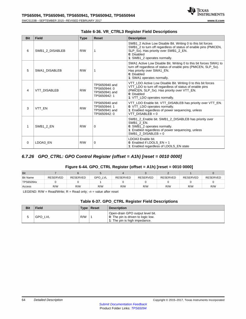
64
TPS65094, TPS650940, TPS650941, TPS650942, TPS650944SWCS133B –SEPTEMBER 2015–REVISED FEBRUARY 2017 www.ti.com
Submit Documentation FeedbackProduct Folder Links: TPS65094
Detailed Description Copyright © 2015–2017, Texas Instruments Incorporated
Table 6-36. VR_CTRL3 Register Field DescriptionsBit Field Type Reset Description
6 SWB1_2_DISABLEB R/W 1
SWB1_2 Active Low Disable Bit. Writing 0 to this bit forcesSWB1_2 to turn off regardless of status of enable pins (PMICEN,SLP_Sx). Has priority over SWB1_2_EN.0: Disabled1: SWB1_2 operates normally.
5 SWA1_DISABLEB R/W 1
SWA1 Active Low Disable Bit. Writing 0 to this bit forces SWA1 toturn off regardless of status of enable pins (PMICEN, SLP_Sx).Has priority over SWA1_EN.0: Disabled1: SWA1 operates normally.
4 VTT_DISABLEB R/W
TPS650940 andTPS650944: 0TPS650941 andTPS650942: 1
VTT_LDO Active Low Disable Bit. Writing 0 to this bit forcesVTT_LDO to turn off regardless of status of enable pins(PMICEN, SLP_Sx). Has priority over VTT_EN.0: Disabled1: VTT_LDO operates normally.
3 VTT_EN R/W
TPS650940 andTPS650944: 1TPS650941 andTPS650942: 0
VTT_LDO Enable bit. VTT_DISABLEB has priority over VTT_EN.0: VTT_LDO operates normally.1: Enabled regardless of power sequencing, unlessVTT_DISABLEB = 0
1 SWB1_2_EN R/W 0
SWB1_2_Enable bit. SWB1_2_DISABLEB has priority overSWB1_2_EN.0: SWB1_2 operates normally.1: Enabled regardless of power sequencing, unlessSWB1_2_DISABLEB = 0
0 LDOA3_EN R/W 0LDOA3 Enable bit.0: Enabled if LDOLS_EN = 11: Enabled regardless of LDOLS_EN state
6.7.26 GPO_CTRL: GPO Control Register (offset = A1h) [reset = 0010 0000]
Figure 6-44. GPO_CTRL Register (offset = A1h) [reset = 0010 0000]Bit 7 6 5 4 3 2 1 0Bit Name RESERVED RESERVED GPO_LVL RESERVED RESERVED RESERVED RESERVED RESERVEDTPS65094x 0 0 1 0 0 0 0 0Access R/W R/W R/W R/W R/W R/W R/W R/W
LEGEND: R/W = Read/Write; R = Read only; -n = value after reset
Table 6-37. GPO_CTRL Register Field DescriptionsBit Field Type Reset Description
5 GPO_LVL R/W 1Open-drain GPO output level bit.0: The pin is driven to logic low.1: The pin is high impedance.
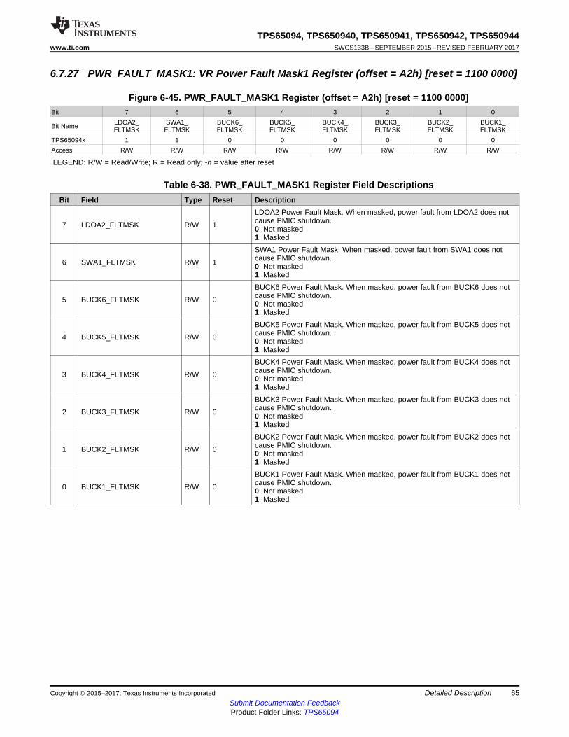
65
TPS65094, TPS650940, TPS650941, TPS650942, TPS650944www.ti.com SWCS133B –SEPTEMBER 2015–REVISED FEBRUARY 2017
Submit Documentation FeedbackProduct Folder Links: TPS65094
Detailed DescriptionCopyright © 2015–2017, Texas Instruments Incorporated
6.7.27 PWR_FAULT_MASK1: VR Power Fault Mask1 Register (offset = A2h) [reset = 1100 0000]
Figure 6-45. PWR_FAULT_MASK1 Register (offset = A2h) [reset = 1100 0000]Bit 7 6 5 4 3 2 1 0
Bit Name LDOA2_FLTMSK
SWA1_FLTMSK
BUCK6_FLTMSK
BUCK5_FLTMSK
BUCK4_FLTMSK
BUCK3_FLTMSK
BUCK2_FLTMSK
BUCK1_FLTMSK
TPS65094x 1 1 0 0 0 0 0 0Access R/W R/W R/W R/W R/W R/W R/W R/W
LEGEND: R/W = Read/Write; R = Read only; -n = value after reset
Table 6-38. PWR_FAULT_MASK1 Register Field DescriptionsBit Field Type Reset Description
7 LDOA2_FLTMSK R/W 1
LDOA2 Power Fault Mask. When masked, power fault from LDOA2 does notcause PMIC shutdown.0: Not masked1: Masked
6 SWA1_FLTMSK R/W 1
SWA1 Power Fault Mask. When masked, power fault from SWA1 does notcause PMIC shutdown.0: Not masked1: Masked
5 BUCK6_FLTMSK R/W 0
BUCK6 Power Fault Mask. When masked, power fault from BUCK6 does notcause PMIC shutdown.0: Not masked1: Masked
4 BUCK5_FLTMSK R/W 0
BUCK5 Power Fault Mask. When masked, power fault from BUCK5 does notcause PMIC shutdown.0: Not masked1: Masked
3 BUCK4_FLTMSK R/W 0
BUCK4 Power Fault Mask. When masked, power fault from BUCK4 does notcause PMIC shutdown.0: Not masked1: Masked
2 BUCK3_FLTMSK R/W 0
BUCK3 Power Fault Mask. When masked, power fault from BUCK3 does notcause PMIC shutdown.0: Not masked1: Masked
1 BUCK2_FLTMSK R/W 0
BUCK2 Power Fault Mask. When masked, power fault from BUCK2 does notcause PMIC shutdown.0: Not masked1: Masked
0 BUCK1_FLTMSK R/W 0
BUCK1 Power Fault Mask. When masked, power fault from BUCK1 does notcause PMIC shutdown.0: Not masked1: Masked
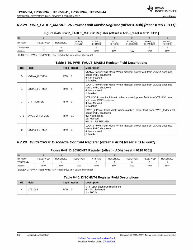
66
TPS65094, TPS650940, TPS650941, TPS650942, TPS650944SWCS133B –SEPTEMBER 2015–REVISED FEBRUARY 2017 www.ti.com
Submit Documentation FeedbackProduct Folder Links: TPS65094
Detailed Description Copyright © 2015–2017, Texas Instruments Incorporated
6.7.28 PWR_FAULT_MASK2: VR Power Fault Mask2 Register (offset = A3h) [reset = 0011 0111]
Figure 6-46. PWR_FAULT_MASK2 Register (offset = A3h) [reset = 0011 0111]Bit 7 6 5 4 3 2 1 0
Bit Name RESERVED RESERVED V5ANA_FLTMSK
LDOA1_FLTMSK
VTT_FLTMSK
SWB1_2_FLTMSK[1]
SWB1_2_FLTMSK[0]
LDOA3_FLTMSK
TPS65094x 0 0 1 1 0 1 1 1Access R R/W R/W R/W R/W R/W R/W R/W
LEGEND: R/W = Read/Write; R = Read only; -n = value after reset
Table 6-39. PWR_FAULT_MASK2 Register Field DescriptionsBit Field Type Reset Description
5 V5ANA_FLTMSK R/W 1
V5ANA Power Fault Mask. When masked, power fault from V5ANA does notcause PMIC shutdown.0: Not masked1: Masked
4 LDOA1_FLTMSK R/W 1
LDOA1 Power Fault Mask. When masked, power fault from LDOA1 does notcause PMIC shutdown.0: Not masked1: Masked
3 VTT_FLTMSK R/W 0
VTT LDO Power Fault Mask. When masked, power fault from VTT LDO doesnot cause PMIC shutdown.0: Not Masked1: Masked
2–1 SWB1_2_FLTMSK R/W 11
SWB1_2 Power Fault Mask. When masked, power fault from SWB1_2 does notcause PMIC shutdown.00: Not masked11: Masked01-10 = RESERVED
0 LDOA3_FLTMSK R/W 1
LDOA3 Power Fault Mask. When masked, power fault from LDOA3 does notcause PMIC shutdown.0: Not masked1: Masked
6.7.29 DISCHCNT4: Discharge Control4 Register (offset = ADh) [reset = 0110 0001]
Figure 6-47. DISCHCNT4 Register (offset = ADh) [reset = 0110 0001]Bit 7 6 5 4 3 2 1 0Bit Name RESERVED RESERVED RESERVED VTT_DIS RESERVED RESERVED RESERVED RESERVEDTPS65094x 0 1 1 0 0 0 0 1Access R/W R/W R/W R/W R/W R/W R/W R/W
LEGEND: R/W = Read/Write; R = Read only; -n = value after reset
Table 6-40. DISCHNT4 Register Field DescriptionsBit Field Type Reset Description
4 VTT_DIS R/W 0VTT_LDO discharge resistance0 = No discharge1 = 100 Ω
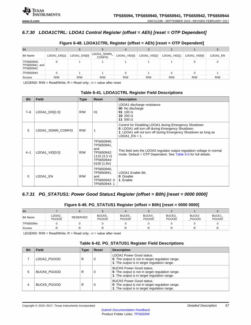
67
TPS65094, TPS650940, TPS650941, TPS650942, TPS650944www.ti.com SWCS133B –SEPTEMBER 2015–REVISED FEBRUARY 2017
Submit Documentation FeedbackProduct Folder Links: TPS65094
Detailed DescriptionCopyright © 2015–2017, Texas Instruments Incorporated
6.7.30 LDOA1CTRL: LDOA1 Control Register (offset = AEh) [reset = OTP Dependent]
Figure 6-48. LDOA1CTRL Register (offset = AEh) [reset = OTP Dependent]Bit 7 6 5 4 3 2 1 0
Bit Name LDOA1_DIS[1] LDOA1_DIS[0] LDOA1_SDWN_CONFIG LDOA1_VID[3] LDOA1_VID[2] LDOA1_VID[1] LDOA1_VID[0] LDOA1_EN
TPS650940,TPS650941, andTPS650942
0 1 1 1 1 1 0 0
TPS650944 0 1 1 0 1 0 0 1Access R/W R/W R/W R/W R/W R/W R/W R/W
LEGEND: R/W = Read/Write; R = Read only; -n = value after reset
Table 6-41. LDOA1CTRL Register Field DescriptionsBit Field Type Reset Description
7–6 LDOA1_DIS[1:0] R/W 01
LDOA1 discharge resistance00: No discharge01: 100 Ω10: 200 Ω11: 500 Ω
5 LDOA1_SDWN_CONFIG R/W 1
Control for Disabling LDOA1 during Emergency Shutdown0: LDOA1 will turn off during Emergency Shutdown.1: LDOA1 will not turn off during Emergency Shutdown as long asLDOA1_EN = 1.
4–1 LDOA1_VID[3:0] R/W
TPS650940,TPS650941,andTPS650942:1110 (3.3 V)TPS650944:0100 (1.8V)
This field sets the LDOA3 regulator output regulation voltage in normalmode. Default = OTP Dependent. See Table 6-5 for full details.
0 LDOA1_EN R/W
TPS650940,TPS650941,andTPS650942: 0TPS650944: 1
LDOA1 Enable Bit.0: Disable1: Enable
6.7.31 PG_STATUS1: Power Good Status1 Register (offset = B0h) [reset = 0000 0000]
Figure 6-49. PG_STATUS1 Register (offset = B0h) [reset = 0000 0000]Bit 7 6 5 4 3 2 1 0
Bit Name LDOA2_PGOOD RESERVED BUCK6_
PGOODBUCK5_PGOOD
BUCK4_PGOOD
BUCK3_PGOOD
BUCK2_PGOOD
BUCK1_PGOOD
TPS65094x 0 0 0 0 0 0 0 0Access R R R R R R R R
LEGEND: R/W = Read/Write; R = Read only; -n = value after reset
Table 6-42. PG_STATUS1 Register Field DescriptionsBit Field Type Reset Description
7 LDOA2_PGOOD R 0LDOA2 Power Good status.0: The output is not in target regulation range.1: The output is in target regulation range.
5 BUCK6_PGOOD R 0BUCK6 Power Good status.0: The output is not in target regulation range.1: The output is in target regulation range.
4 BUCK5_PGOOD R 0BUCK5 Power Good status.0: The output is not in target regulation range.1: The output is in target regulation range.
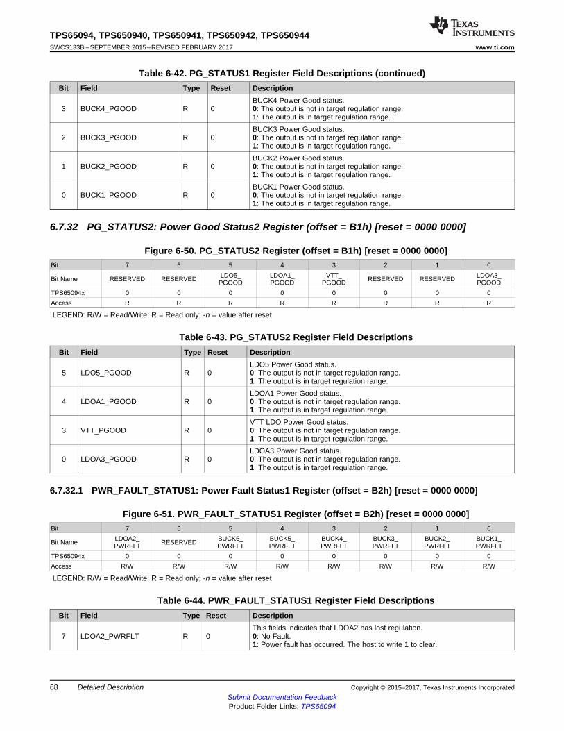
68
TPS65094, TPS650940, TPS650941, TPS650942, TPS650944SWCS133B –SEPTEMBER 2015–REVISED FEBRUARY 2017 www.ti.com
Submit Documentation FeedbackProduct Folder Links: TPS65094
Detailed Description Copyright © 2015–2017, Texas Instruments Incorporated
Table 6-42. PG_STATUS1 Register Field Descriptions (continued)Bit Field Type Reset Description
3 BUCK4_PGOOD R 0BUCK4 Power Good status.0: The output is not in target regulation range.1: The output is in target regulation range.
2 BUCK3_PGOOD R 0BUCK3 Power Good status.0: The output is not in target regulation range.1: The output is in target regulation range.
1 BUCK2_PGOOD R 0BUCK2 Power Good status.0: The output is not in target regulation range.1: The output is in target regulation range.
0 BUCK1_PGOOD R 0BUCK1 Power Good status.0: The output is not in target regulation range.1: The output is in target regulation range.
6.7.32 PG_STATUS2: Power Good Status2 Register (offset = B1h) [reset = 0000 0000]
Figure 6-50. PG_STATUS2 Register (offset = B1h) [reset = 0000 0000]Bit 7 6 5 4 3 2 1 0
Bit Name RESERVED RESERVED LDO5_PGOOD
LDOA1_PGOOD
VTT_PGOOD RESERVED RESERVED LDOA3_
PGOODTPS65094x 0 0 0 0 0 0 0 0Access R R R R R R R R
LEGEND: R/W = Read/Write; R = Read only; -n = value after reset
Table 6-43. PG_STATUS2 Register Field DescriptionsBit Field Type Reset Description
5 LDO5_PGOOD R 0LDO5 Power Good status.0: The output is not in target regulation range.1: The output is in target regulation range.
4 LDOA1_PGOOD R 0LDOA1 Power Good status.0: The output is not in target regulation range.1: The output is in target regulation range.
3 VTT_PGOOD R 0VTT LDO Power Good status.0: The output is not in target regulation range.1: The output is in target regulation range.
0 LDOA3_PGOOD R 0LDOA3 Power Good status.0: The output is not in target regulation range.1: The output is in target regulation range.
6.7.32.1 PWR_FAULT_STATUS1: Power Fault Status1 Register (offset = B2h) [reset = 0000 0000]
Figure 6-51. PWR_FAULT_STATUS1 Register (offset = B2h) [reset = 0000 0000]Bit 7 6 5 4 3 2 1 0
Bit Name LDOA2_PWRFLT RESERVED BUCK6_
PWRFLTBUCK5_PWRFLT
BUCK4_PWRFLT
BUCK3_PWRFLT
BUCK2_PWRFLT
BUCK1_PWRFLT
TPS65094x 0 0 0 0 0 0 0 0Access R/W R/W R/W R/W R/W R/W R/W R/W
LEGEND: R/W = Read/Write; R = Read only; -n = value after reset
Table 6-44. PWR_FAULT_STATUS1 Register Field DescriptionsBit Field Type Reset Description
7 LDOA2_PWRFLT R 0This fields indicates that LDOA2 has lost regulation.0: No Fault.1: Power fault has occurred. The host to write 1 to clear.
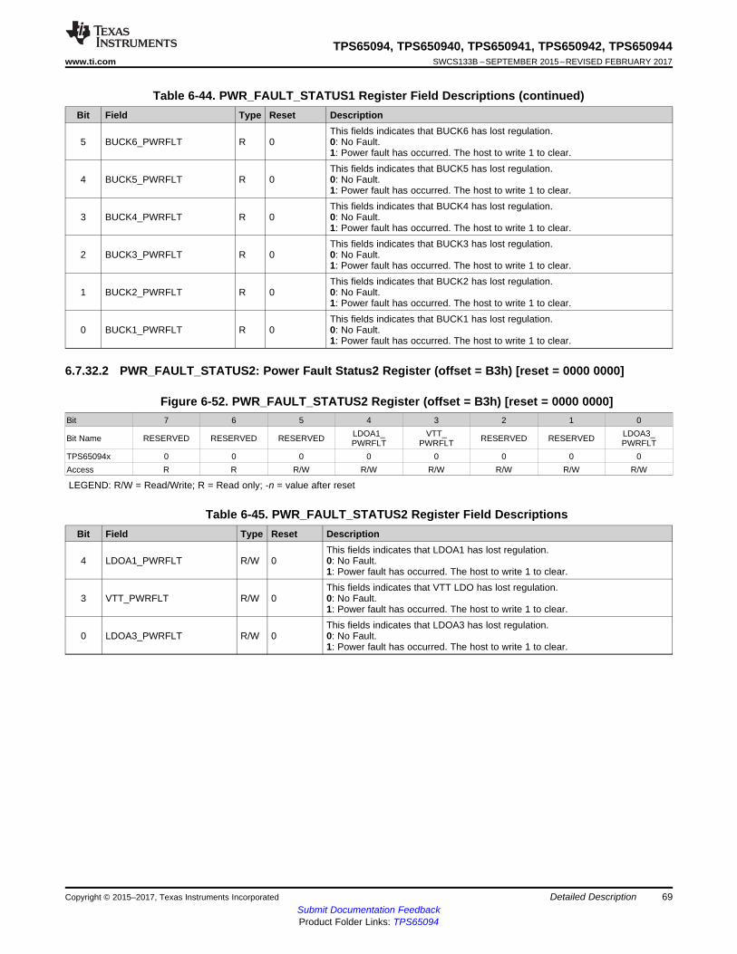
69
TPS65094, TPS650940, TPS650941, TPS650942, TPS650944www.ti.com SWCS133B –SEPTEMBER 2015–REVISED FEBRUARY 2017
Submit Documentation FeedbackProduct Folder Links: TPS65094
Detailed DescriptionCopyright © 2015–2017, Texas Instruments Incorporated
Table 6-44. PWR_FAULT_STATUS1 Register Field Descriptions (continued)Bit Field Type Reset Description
5 BUCK6_PWRFLT R 0This fields indicates that BUCK6 has lost regulation.0: No Fault.1: Power fault has occurred. The host to write 1 to clear.
4 BUCK5_PWRFLT R 0This fields indicates that BUCK5 has lost regulation.0: No Fault.1: Power fault has occurred. The host to write 1 to clear.
3 BUCK4_PWRFLT R 0This fields indicates that BUCK4 has lost regulation.0: No Fault.1: Power fault has occurred. The host to write 1 to clear.
2 BUCK3_PWRFLT R 0This fields indicates that BUCK3 has lost regulation.0: No Fault.1: Power fault has occurred. The host to write 1 to clear.
1 BUCK2_PWRFLT R 0This fields indicates that BUCK2 has lost regulation.0: No Fault.1: Power fault has occurred. The host to write 1 to clear.
0 BUCK1_PWRFLT R 0This fields indicates that BUCK1 has lost regulation.0: No Fault.1: Power fault has occurred. The host to write 1 to clear.
6.7.32.2 PWR_FAULT_STATUS2: Power Fault Status2 Register (offset = B3h) [reset = 0000 0000]
Figure 6-52. PWR_FAULT_STATUS2 Register (offset = B3h) [reset = 0000 0000]Bit 7 6 5 4 3 2 1 0
Bit Name RESERVED RESERVED RESERVED LDOA1_PWRFLT
VTT_PWRFLT RESERVED RESERVED LDOA3_
PWRFLTTPS65094x 0 0 0 0 0 0 0 0Access R R R/W R/W R/W R/W R/W R/W
LEGEND: R/W = Read/Write; R = Read only; -n = value after reset
Table 6-45. PWR_FAULT_STATUS2 Register Field DescriptionsBit Field Type Reset Description
4 LDOA1_PWRFLT R/W 0This fields indicates that LDOA1 has lost regulation.0: No Fault.1: Power fault has occurred. The host to write 1 to clear.
3 VTT_PWRFLT R/W 0This fields indicates that VTT LDO has lost regulation.0: No Fault.1: Power fault has occurred. The host to write 1 to clear.
0 LDOA3_PWRFLT R/W 0This fields indicates that LDOA3 has lost regulation.0: No Fault.1: Power fault has occurred. The host to write 1 to clear.
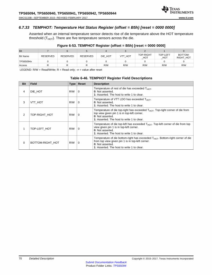
70
TPS65094, TPS650940, TPS650941, TPS650942, TPS650944SWCS133B –SEPTEMBER 2015–REVISED FEBRUARY 2017 www.ti.com
Submit Documentation FeedbackProduct Folder Links: TPS65094
Detailed Description Copyright © 2015–2017, Texas Instruments Incorporated
6.7.33 TEMPHOT: Temperature Hot Status Register (offset = B5h) [reset = 0000 0000]Asserted when an internal temperature sensor detects rise of die temperature above the HOT temperaturethreshold (THOT). There are five temperature sensors across the die.
Figure 6-53. TEMPHOT Register (offset = B5h) [reset = 0000 0000]Bit 7 6 5 4 3 2 1 0
Bit Name RESERVED RESERVED RESERVED DIE_HOT VTT_HOT TOP-RIGHT_HOT
TOP-LEFT_HOT
BOTTOM-RIGHT_HOT
TPS65094x 0 0 0 0 0 0 0 0Access R R R R/W R/W R/W R/W R/W
LEGEND: R/W = Read/Write; R = Read only; -n = value after reset
Table 6-46. TEMPHOT Register Field DescriptionsBit Field Type Reset Description
4 DIE_HOT R/W 0Temperature of rest of die has exceeded THOT.0: Not asserted.1: Asserted. The host to write 1 to clear.
3 VTT_HOT R/W 0Temperature of VTT LDO has exceeded THOT.0: Not asserted.1: Asserted. The host to write 1 to clear.
2 TOP-RIGHT_HOT R/W 0
Temperature of die top-right has exceeded THOT. Top-right corner of die fromtop view given pin 1 is in top-left corner.0: Not asserted.1: Asserted. The host to write 1 to clear.
1 TOP-LEFT_HOT R/W 0
Temperature of die top-left has exceeded THOT. Top-left corner of die from topview given pin 1 is in top-left corner.0: Not asserted.1: Asserted. The host to write 1 to clear.
0 BOTTOM-RIGHT_HOT R/W 0
Temperature of die bottom-right has exceeded THOT. Bottom-right corner of diefrom top view given pin 1 is in top-left corner.0: Not asserted.1: Asserted. The host to write 1 to clear.
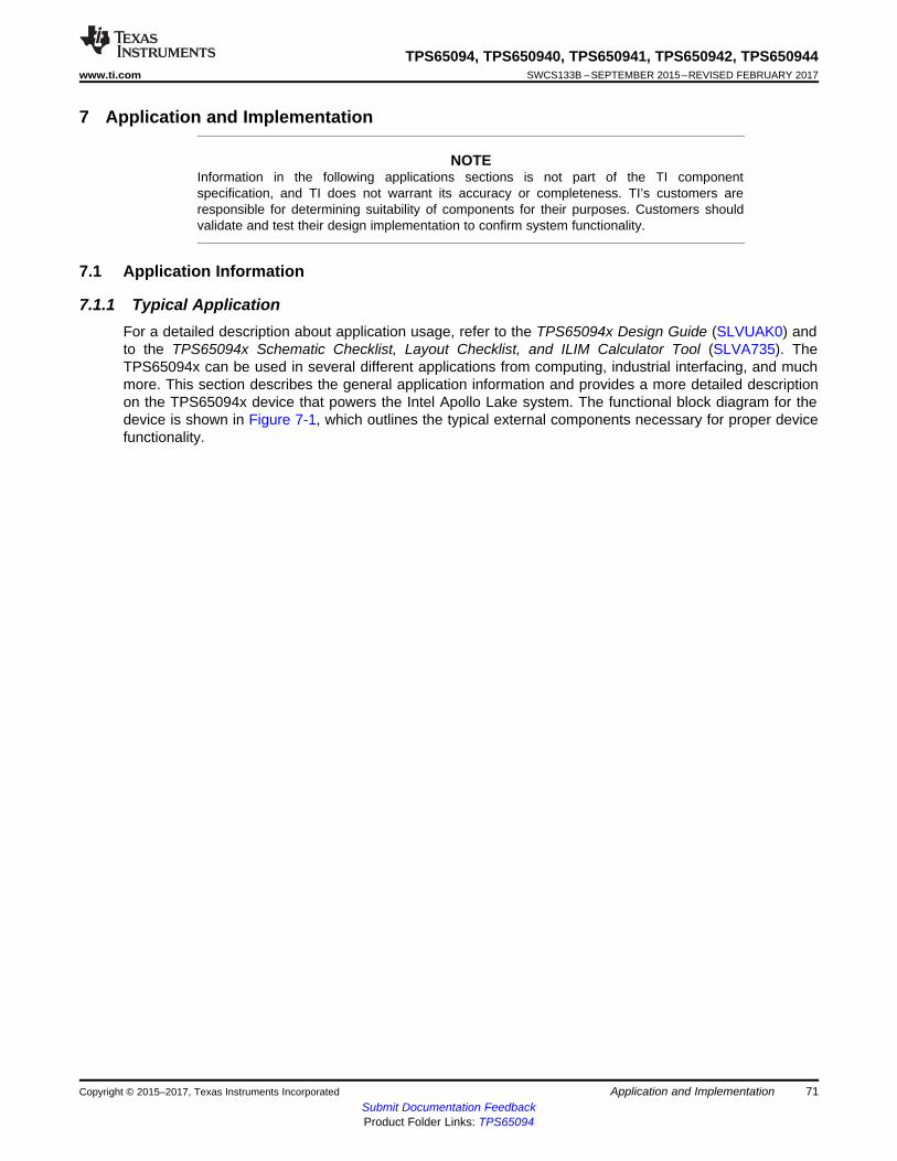
71
TPS65094, TPS650940, TPS650941, TPS650942, TPS650944www.ti.com SWCS133B –SEPTEMBER 2015–REVISED FEBRUARY 2017
Submit Documentation FeedbackProduct Folder Links: TPS65094
Application and ImplementationCopyright © 2015–2017, Texas Instruments Incorporated
7 Application and Implementation
NOTEInformation in the following applications sections is not part of the TI componentspecification, and TI does not warrant its accuracy or completeness. TI’s customers areresponsible for determining suitability of components for their purposes. Customers shouldvalidate and test their design implementation to confirm system functionality.
7.1 Application Information
7.1.1 Typical ApplicationFor a detailed description about application usage, refer to the TPS65094x Design Guide (SLVUAK0) andto the TPS65094x Schematic Checklist, Layout Checklist, and ILIM Calculator Tool (SLVA735). TheTPS65094x can be used in several different applications from computing, industrial interfacing, and muchmore. This section describes the general application information and provides a more detailed descriptionon the TPS65094x device that powers the Intel Apollo Lake system. The functional block diagram for thedevice is shown in Figure 7-1, which outlines the typical external components necessary for proper devicefunctionality.
IRQB
ControlOutputs
REFSYS
REGISTERS
Digital Core
INT
ER
RU
PT
_CN
TL
Thermalmonitoring
Thermal shutdown
OTP
TEST CTRL
I2C CTRL
SLP_S0B
PCH_PWROK
RSMRSTB
PROCHOT
InternalInterrupt Events
<PGND_BUCK3>
BUCK3Default: 1.05 V
3 A
VREF
BUCK1Default: 1V
Typical Application
Usage:0.5 V to 1.45 V
(DVS)5 A
VSYS
LDOA20.7 V to 1.5 V
600 mA
ControlInputs
SoC
VSYS
LOAD SWB2400 mA
PMICEN
SLP_S3B
SLP_S4B
LDOLS_EN(a)
SWA1_EN(b)
THERMTRIPB
VSYS
LDO5
LDO3P3
V5ANABUCK5V
nPUC
BOOT1
DRVH1
SW1
DRVL1
FBVOUT1
PGNDSNS1
ILIM1
BUCK2Default: 0V
Typical Application
Usage:0.5 V to 1.45 V
(DVS)21 A
VSYS
BOOT2
DRVH2
SW2
DRVL2
FBVOUT2
PGNDSNS2
ILIM2
PVIN3
LX3
FB3
BUCK5V
<PGND_BUCK4>
BUCK4Default: 1.8 V
2 A
PVIN4
LX4
FB4
<PGND_BUCK5>
BUCK5Default: 1.24 V
2 A
PVIN5
LX5
FB5
BUCK5V
BUCK6Default: OTP Dependent
7 A
VSYS
BOOT6
DRVH6
SW6
DRVL6
FBVOUT6
PGNDSNS6
ILIM6
LDO5V
VNN
VTT_LDO½ × VDDQ
ILIM set by OTP
VDDQ
VTT
PVINVTT
VTT
VTTFB
DR
V5V
_1_6
DR
V5V
_2_A
1
LDOA11.35 V to 3.3 V
1.8 V(b)
200 mA
LDO
A1
V1P8A
CLK
DATA
LOAD SWB1400 mA
LOAD SWA1300 mA
LDOA30.7 V to 1.5 V
600 mA
SW
B2
PV
INS
WB
1_B
2
SW
B1
SW
A1
PV
INS
WA
1
LDO
A3
PV
INLD
OA
2_A
3
LDO
A2
AGND
0.5
V t
o 3
.3 V
V1P
8U(1
)
SW
A1
VCCGI
VCCRAM
V1P8A
V1P24A
FBGND2
VSET
EN
VSET
EN
VSET
EN
VSET
EN
VSET
EN
VSET
EN
VS
ET
EN
VS
ET
EN
EN
EN
EN
EN
EN
LDO5V
BUCK5V
EC
0.5 V to 3.3 V
V1P8A
GPO
Dashed connections optional.Refer to Pin Attributes for
connection if unused.
SW
B1_
2(2)
(1) LPDDR3 and LPDDR4(2) DDR3L
(a) LDOA1 1RW�³$OZD\V�2Q´(b) LDOA1 ³$OZD\V�2Q´
Optional(a)
Required(b)
V1P8A(1)
0.5 V to 3.3 V(2)
Copyright © 2016, Texas Instruments Incorporated
72
TPS65094, TPS650940, TPS650941, TPS650942, TPS650944SWCS133B –SEPTEMBER 2015–REVISED FEBRUARY 2017 www.ti.com
Submit Documentation FeedbackProduct Folder Links: TPS65094
Application and Implementation Copyright © 2015–2017, Texas Instruments Incorporated
Figure 7-1. Functional Block Diagram
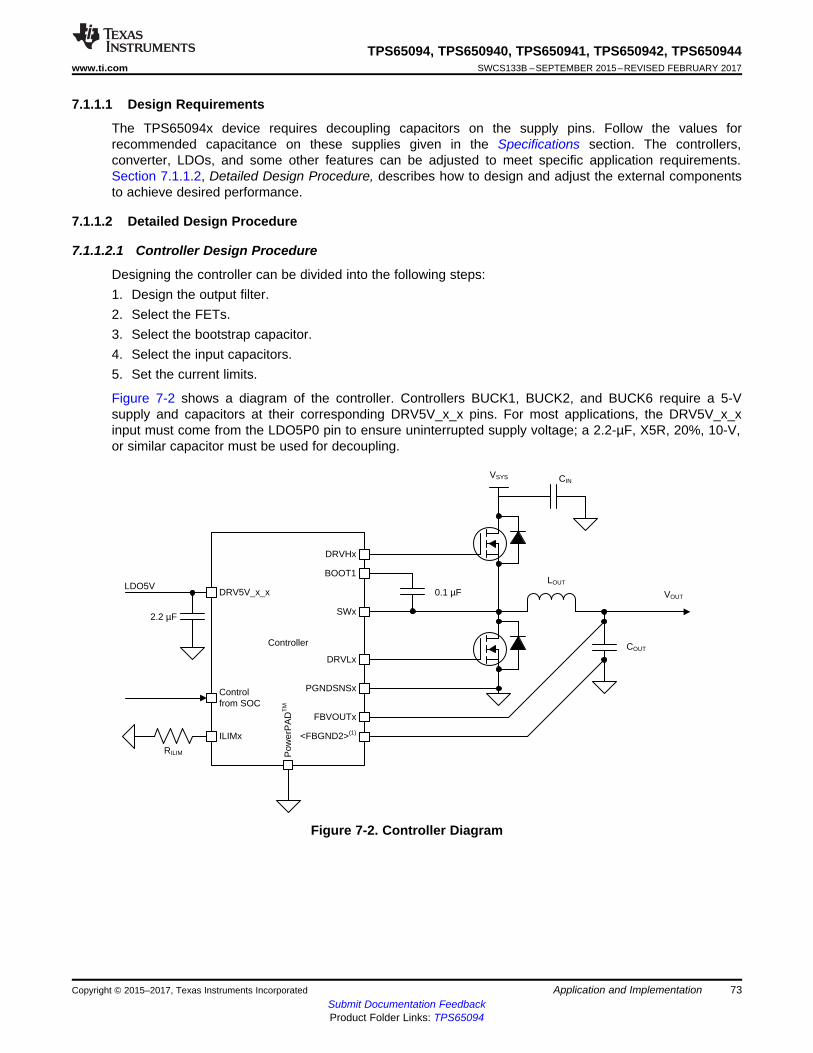
Controller
DRVHx
DRVLx
BOOT1
SWx
FBVOUTx
<FBGND2>(1)
PGNDSNSx
VOUT
CINVSYS
0.1 µF
COUT
LOUT
ILIMx
DRV5V_x_x
2.2 µF
LDO5V
Control from SOC
Pow
erP
AD
TM
RILIM
73
TPS65094, TPS650940, TPS650941, TPS650942, TPS650944www.ti.com SWCS133B –SEPTEMBER 2015–REVISED FEBRUARY 2017
Submit Documentation FeedbackProduct Folder Links: TPS65094
Application and ImplementationCopyright © 2015–2017, Texas Instruments Incorporated
7.1.1.1 Design Requirements
The TPS65094x device requires decoupling capacitors on the supply pins. Follow the values forrecommended capacitance on these supplies given in the Specifications section. The controllers,converter, LDOs, and some other features can be adjusted to meet specific application requirements.Section 7.1.1.2, Detailed Design Procedure, describes how to design and adjust the external componentsto achieve desired performance.
7.1.1.2 Detailed Design Procedure
7.1.1.2.1 Controller Design Procedure
Designing the controller can be divided into the following steps:1. Design the output filter.2. Select the FETs.3. Select the bootstrap capacitor.4. Select the input capacitors.5. Set the current limits.
Figure 7-2 shows a diagram of the controller. Controllers BUCK1, BUCK2, and BUCK6 require a 5-Vsupply and capacitors at their corresponding DRV5V_x_x pins. For most applications, the DRV5V_x_xinput must come from the LDO5P0 pin to ensure uninterrupted supply voltage; a 2.2-µF, X5R, 20%, 10-V,or similar capacitor must be used for decoupling.
Figure 7-2. Controller Diagram
IN OUT OUTL(MAX) OUT(MAX)
IN sw
(V V ) VI I
2 V f L
� u �
u u u
OUT IN OUT
IN sw OUT(MAX) IND
V (V V )L
V f I K
´ -
=
´ ´ ´
74
TPS65094, TPS650940, TPS650941, TPS650942, TPS650944SWCS133B –SEPTEMBER 2015–REVISED FEBRUARY 2017 www.ti.com
Submit Documentation FeedbackProduct Folder Links: TPS65094
Application and Implementation Copyright © 2015–2017, Texas Instruments Incorporated
7.1.1.2.1.1 Selecting the Output Capacitors
TI recommends using ceramic capacitors with low ESR values to provide the lowest output voltage ripple.The output capacitor requires either an X7R or an X5R dielectric. Capacitors with Y5V or Z5U dielectricsdisplay a wide variation in capacitance over temperature and become resistive at high frequencies.
At light load currents, the controller operates in PFM mode, and the output voltage ripple is dependent onthe output-capacitor value and the PFM peak inductor current. Higher output-capacitor values minimizethe voltage ripple in PFM mode. To achieve specified regulation performance and low output voltageripple, the DC-bias characteristic of ceramic capacitors must be considered. The effective capacitance ofceramic capacitors drops with increasing DC bias voltage.
For the output capacitors of the BUCK controllers, TI recommends placing small ceramic capacitorsbetween the inductor and load with many vias to the PGND plane. This solution typically provides thesmallest and lowest cost solution available for DCAP2 controllers.
To meet the transient specifications, the output capacitance must equal or exceed the minimumcapacitance listed in the electrical characteristics table for BUCK1, BUCK2, and BUCK6 (assuming qualitylayout techniques are followed). See Section 5.7, Electrical Characteristics: Buck Controllers.
7.1.1.2.1.2 Selecting the Inductor
An inductor must be placed between the external FETs and the output capacitors. Together, the inductorand output capacitors make the double-pole that contributes to stability. In addition, the inductor isresponsible for the output ripple, efficiency, and transient performance. When the inductance increases,the ripple current decreases, which typically results in an increased efficiency. However, with an increasein inductance, the transient performance decreases. Finally, the inductor selected must be rated forappropriate saturation current, core losses, and DC resistance (DCR).
Equation 3 shows the calculation for the recommended inductance for the controller.
where• VOUT is the typical output voltage.• VIN is the typical input voltage.• fSW is the typical switching frequency.• IOUT(MAX) is the maximum load current.• KIND is the ratio of ILripple to the IOUT(MAX). For this application, TI recommends that KIND is set to a value
from 0.2 to 0.4. (3)
With the chosen inductance value and the peak current for the inductor in steady state operation, IL(max)can be calculated using Equation 4. The rated saturation current of the inductor must be higher than theIL(MAX) current.
(4)
Following the previous equations, Table 7-1 lists the preferred inductor selected for the controllers..
Table 7-1. Recommended Inductors
MANUFACTURER PART NUMBER VALUE SIZE HEIGHTCyntec PIMB061H 0.47 µH 6.8 mm × 7.3 mm 1.8 mmCyntec PIMB062D 0.22 µH 6.8 mm × 7.3 mm 2.4 mm
75
TPS65094, TPS650940, TPS650941, TPS650942, TPS650944www.ti.com SWCS133B –SEPTEMBER 2015–REVISED FEBRUARY 2017
Submit Documentation FeedbackProduct Folder Links: TPS65094
Application and ImplementationCopyright © 2015–2017, Texas Instruments Incorporated
7.1.1.2.1.3 Selecting the FETs
This controller is designed to drive two NMOS FETs. Typically, lower RDSON values are better forimproving the overall efficiency of the controller. However, higher gate-charge thresholds result in lowerefficiency, so the two must be balanced for optimal performance. As the RDSON for the low-side FETdecreases, the minimum current limit increases; therefore, ensure selection of the appropriate values forthe FETs, inductor, output capacitors, and current-limit resistor. TI's CSD87331Q3D, CSD87381P, andCSD87588N devices are recommended for the controllers, depending on the required maximum current.
7.1.1.2.1.4 Bootstrap Capacitor
To ensure the internal high-side gate drivers are supplied with a stable low-noise supply voltage, acapacitor must be connected between the SWx pins and the respective BOOTx pins. TI recommendsplacing ceramic capacitors with the value of 0.1 µF for the controllers. During testing, a 0.1-µF, size 0402,10-V capacitor is used for the controllers.
TI recommends reserving a small resistor in series with the bootstrap capacitor in case the turnon andturnoff of the FETs must be slowed to reduce voltage ringing on the switch node, which is a commonpractice for controller design.
7.1.1.2.1.5 Selecting the Input Capacitors
Due to the nature of the switching controller with a pulsating input current, a low-ESR input capacitor isrequired for best input-voltage filtering and also for minimizing the interference with other circuits causedby high input-voltage spikes. For the controller, a typical 2.2-µF capacitor can be used for the DRV5V_x_xpin to handle the transients on the driver. For the FET input, 10 µF of input capacitance (after derating) isrecommended for most applications. To achieve the low-ESR requirement, a ceramic capacitor isrecommended. However, the voltage rating and DC-bias characteristic of ceramic capacitors must beconsidered. For better input-voltage filtering, the input capacitor can be increased without any limit.
7.1.1.2.1.5.1 Setting the Current Limit
The current-limiting resistor value must be chosen based on Equation 1.
NOTEUse the correct value for the ceramic capacitor capacitance after derating to achieve therecommended input capacitance.
TI recommends placing a ceramic capacitor as close as possible to the FET across the respective VSYSand PGND pins of the FETs. The preferred capacitors for the controllers are two MurataGRM21BR61E226ME44: 22 µF, 0805, 25 V, ±20%, or similar capacitors.
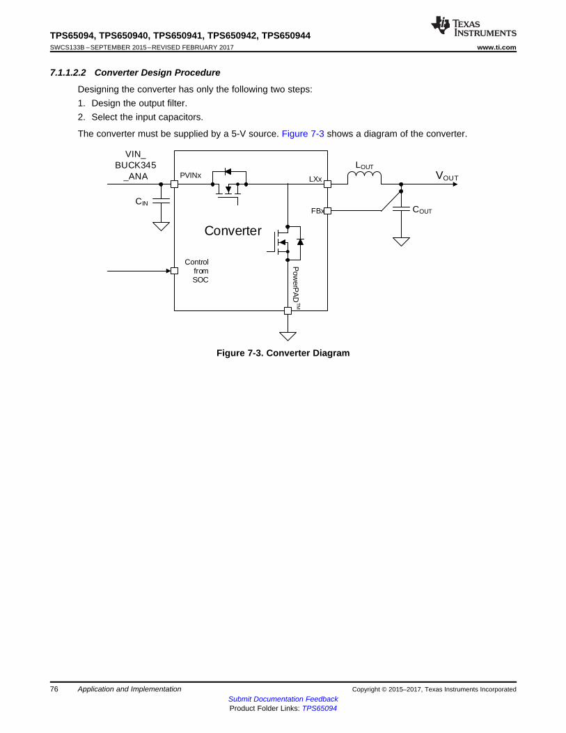
Converter
LXx
FBx
Pow
erPA
DTM
PVINx
Control from SOC
CIN
VIN_BUCK345
_ANA VOUT
COUT
LOUT
76
TPS65094, TPS650940, TPS650941, TPS650942, TPS650944SWCS133B –SEPTEMBER 2015–REVISED FEBRUARY 2017 www.ti.com
Submit Documentation FeedbackProduct Folder Links: TPS65094
Application and Implementation Copyright © 2015–2017, Texas Instruments Incorporated
7.1.1.2.2 Converter Design Procedure
Designing the converter has only the following two steps:1. Design the output filter.2. Select the input capacitors.
The converter must be supplied by a 5-V source. Figure 7-3 shows a diagram of the converter.
Figure 7-3. Converter Diagram
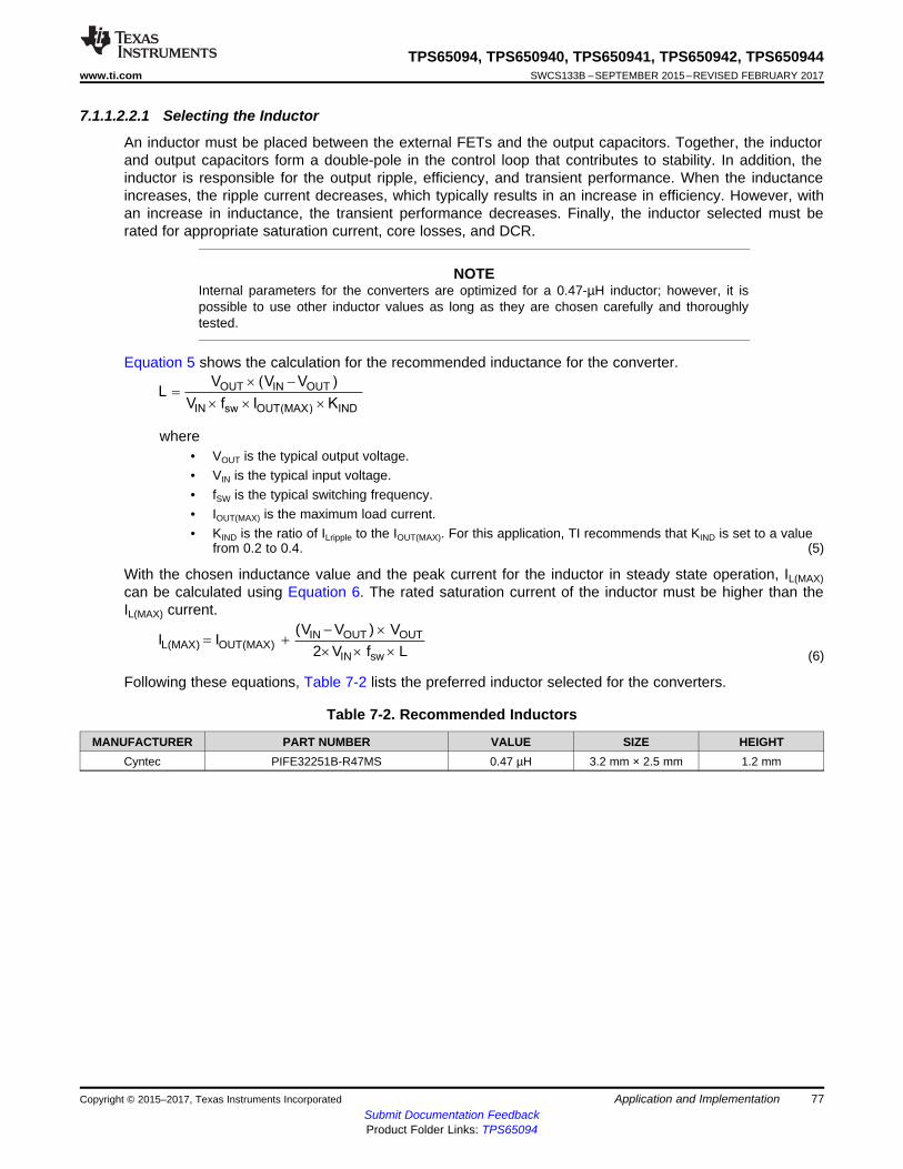
IN OUT OUTL(MAX) OUT(MAX)
IN sw
(V V ) VI I
2 V f L
� u �
u u u
OUT IN OUT
IN sw OUT(MAX) IND
V (V V )L
V f I K
´ -
=
´ ´ ´
77
TPS65094, TPS650940, TPS650941, TPS650942, TPS650944www.ti.com SWCS133B –SEPTEMBER 2015–REVISED FEBRUARY 2017
Submit Documentation FeedbackProduct Folder Links: TPS65094
Application and ImplementationCopyright © 2015–2017, Texas Instruments Incorporated
7.1.1.2.2.1 Selecting the Inductor
An inductor must be placed between the external FETs and the output capacitors. Together, the inductorand output capacitors form a double-pole in the control loop that contributes to stability. In addition, theinductor is responsible for the output ripple, efficiency, and transient performance. When the inductanceincreases, the ripple current decreases, which typically results in an increase in efficiency. However, withan increase in inductance, the transient performance decreases. Finally, the inductor selected must berated for appropriate saturation current, core losses, and DCR.
NOTEInternal parameters for the converters are optimized for a 0.47-µH inductor; however, it ispossible to use other inductor values as long as they are chosen carefully and thoroughlytested.
Equation 5 shows the calculation for the recommended inductance for the converter.
where• VOUT is the typical output voltage.• VIN is the typical input voltage.• fSW is the typical switching frequency.• IOUT(MAX) is the maximum load current.• KIND is the ratio of ILripple to the IOUT(MAX). For this application, TI recommends that KIND is set to a value
from 0.2 to 0.4. (5)
With the chosen inductance value and the peak current for the inductor in steady state operation, IL(MAX)can be calculated using Equation 6. The rated saturation current of the inductor must be higher than theIL(MAX) current.
(6)
Following these equations, Table 7-2 lists the preferred inductor selected for the converters.
Table 7-2. Recommended Inductors
MANUFACTURER PART NUMBER VALUE SIZE HEIGHTCyntec PIFE32251B-R47MS 0.47 µH 3.2 mm × 2.5 mm 1.2 mm
78
TPS65094, TPS650940, TPS650941, TPS650942, TPS650944SWCS133B –SEPTEMBER 2015–REVISED FEBRUARY 2017 www.ti.com
Submit Documentation FeedbackProduct Folder Links: TPS65094
Application and Implementation Copyright © 2015–2017, Texas Instruments Incorporated
7.1.1.2.2.2 Selecting the Output Capacitors
TI recommends using ceramic capacitors with low-ESR values are recommended to provide the lowestoutput voltage ripple. The output capacitor requires either an X7R or an X5R rating. Y5V and Z5Ucapacitors, aside from the wide variation in capacitance overtemperature, become resistive at highfrequencies.
At light load currents, the converter operates in PFM mode and the output voltage ripple is dependent onthe output-capacitor value and the PFM peak inductor current. Higher output-capacitor values minimizethe voltage ripple in PFM mode. To achieve specified regulation performance and low output voltageripple, the DC-bias characteristic of ceramic capacitors must be considered. The effective capacitance ofceramic capacitors drops with increasing DC-bias voltage.
For the output capacitors of the BUCK converters, TI recommends placing small ceramic capacitorsbetween the inductor and load with many vias to the PGND plane. This solution typically provides thesmallest and lowest-cost solution available for DCAP2 controllers.
To meet the transient specifications, the output capacitance must equal or exceed the minimumcapacitance listed for BUCK3, BUCK4, and BUCK5 (assuming quality layout techniques are followed).
7.1.1.2.2.3 Selecting the Input Capacitors
Due to the nature of the switching converter with a pulsating input current, a low-ESR input capacitor isrequired for best input-voltage filtering and for minimizing the interference with other circuits caused byhigh input-voltage spikes. For the PVINx pin, 2.5 µF of input capacitance (after derating) is required formost applications. A ceramic capacitor is recommended to achieve the low-ESR requirement. However,the voltage rating and DC-bias characteristic of ceramic capacitors must be considered. For better input-voltage filtering, the input capacitor can be increased without any limit.
NOTEUse the correct value for the ceramic capacitor capacitance after derating to achieve therecommended input capacitance.
The preferred capacitor for the converters is one Samsung CL05A106MP5NUNC: 10 µF, 0402, 10 V,±20%, or similar capacitor.
7.1.1.2.3 LDO Design Procedure
The VTT LDO must handle the fast load transients from the DDR memory for termination. Therefore, TIrecommends using ceramic capacitors to maintain a high amount of capacitance with low ESR on the VTTLDO outputs and inputs. The preferred output capacitors for the VTT LDO are the GRM188R60J226MEA0from Murata (22 µF, 0603, 6.3 V, ±20%, or similar capacitors). The preferred input capacitor for the VTTLDO is the CL05A106MP5NUNC from Samsung (10 µF, 0402, 10 V, ±20%, or similar capacitor).
The remaining LDOs must have input and output capacitors chosen based on the values in Section 5.9,Electrical Characteristics: LDOs.
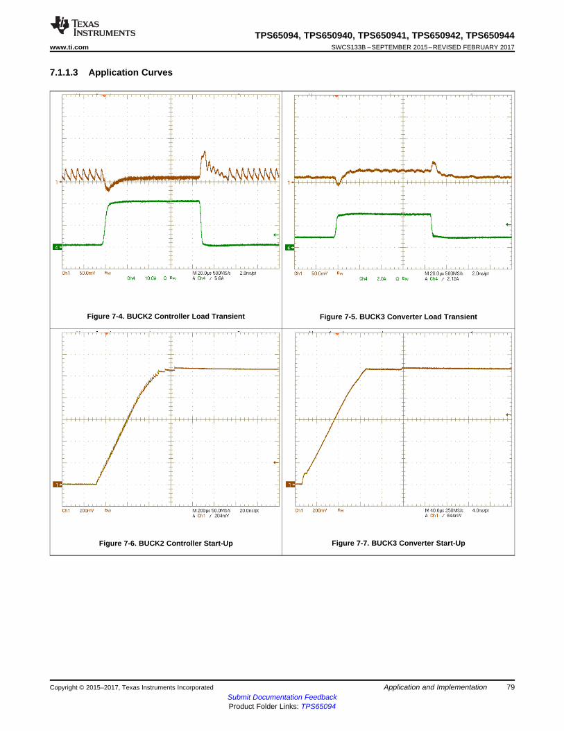
79
TPS65094, TPS650940, TPS650941, TPS650942, TPS650944www.ti.com SWCS133B –SEPTEMBER 2015–REVISED FEBRUARY 2017
Submit Documentation FeedbackProduct Folder Links: TPS65094
Application and ImplementationCopyright © 2015–2017, Texas Instruments Incorporated
7.1.1.3 Application Curves
Figure 7-4. BUCK2 Controller Load Transient Figure 7-5. BUCK3 Converter Load Transient
Figure 7-6. BUCK2 Controller Start-Up Figure 7-7. BUCK3 Converter Start-Up
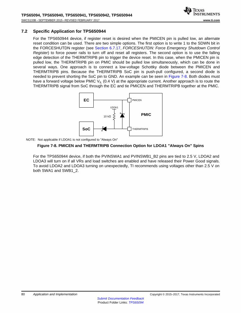
PMIC
SoC
PMICEN
THERMTRIPB
EC
10 k
LDOA1
80
TPS65094, TPS650940, TPS650941, TPS650942, TPS650944SWCS133B –SEPTEMBER 2015–REVISED FEBRUARY 2017 www.ti.com
Submit Documentation FeedbackProduct Folder Links: TPS65094
Application and Implementation Copyright © 2015–2017, Texas Instruments Incorporated
7.2 Specific Application for TPS650944For the TPS650944 device, if register reset is desired when the PMICEN pin is pulled low, an alternatereset condition can be used. There are two simple options. The first option is to write 1 to the SDWN bit inthe FORCESHUTDN register (see Section 6.7.17, FORCESHUTDN: Force Emergency Shutdown ControlRegister) to force power rails to turn off and reset all registers. The second option is to use the fallingedge detection of the THERMTRIPB pin to trigger the device reset. In this case, when the PMICEN pin ispulled low, the THERMTRIPB pin on PMIC should be pulled low simultaneously, which can be done inseveral ways. One approach is to connect a low-voltage Schottky diode between the PMICEN andTHERMTRIPB pins. Because the THERMTRIPB SoC pin is push-pull configured, a second diode isneeded to prevent shorting the SoC pin to GND. An example can be seen in Figure 7-8. Both diodes musthave a forward voltage below PMIC VIL (0.4 V) at the appropriate current. Another approach is to route theTHERMTRIPB signal from SoC through the EC and tie PMICEN and THERMTRIPB together at the PMIC.
NOTE: Not applicable if LDOA1 is not configured to "Always On"
Figure 7-8. PMICEN and THERMTRIPB Connection Option for LDOA1 "Always On" Spins
For the TPS650944 device, if both the PVINSWA1 and PVINSWB1_B2 pins are tied to 2.5 V, LDOA2 andLDOA3 will turn on if all VRs and load switches are enabled and have released their Power Good signals.To avoid LDOA2 and LDOA3 turning on unexpectedly, TI recommends using voltages other than 2.5 V onboth SWA1 and SWB1_2.
81
TPS65094, TPS650940, TPS650941, TPS650942, TPS650944www.ti.com SWCS133B –SEPTEMBER 2015–REVISED FEBRUARY 2017
Submit Documentation FeedbackProduct Folder Links: TPS65094
Power Supply Coupling and Bulk CapacitorsCopyright © 2015–2017, Texas Instruments Incorporated
7.3 Do's and Don'ts• Connect the LDO5V output to the DRV5V_x_x inputs for situations where an external 5-V supply is not
initially available or is not available the entire time PMIC is on. If the external 5-V supply is alwayspresent, then DRV5V_x_x can be directly connected to remove the V5ANA-to-LDO5P0 load switchRDSON.
• Ensure that none of the control pins are potentially floating.• Include 0-Ω resistors on the DRVH and BOOT pins of controllers on prototype boards, which allows for
slowing the controllers if the system is unable to handle the noise generated by the large switching or ifswitching voltage is too large due to layout.
• Do not connect the V5ANA power input to a different source other than PVINx. A mismatch herecauses reference circuits to regulate incorrectly.
• Do not supply the V5ANA power input before the VSYS. Reference biasing of the internal FETs mayturn on the HS FET and pass the input to the output until VSYS is biased.
8 Power Supply Coupling and Bulk Capacitors
This device is designed to work with several different input voltages. The minimum voltage on the VSYSpin is 5.6 V for the device to start up; however, this is a low-power rail. The input to the FETs must befrom 5.4 V to 21 V as long as the proper BOM choices are made. Input to the converters must be5 V. For the device to output maximum power, the input power must be sufficient. For the controllers, VINmust be able to supply up to 5 A (typically), though less is acceptable with higher voltages or less usage.For the converters, PVINx must be able to supply 2 A (typically).
A best practice here is to determine power usage by the system and back-calculate the necessary powerinput based on expected efficiency values.
82
TPS65094, TPS650940, TPS650941, TPS650942, TPS650944SWCS133B –SEPTEMBER 2015–REVISED FEBRUARY 2017 www.ti.com
Submit Documentation FeedbackProduct Folder Links: TPS65094
Layout Copyright © 2015–2017, Texas Instruments Incorporated
9 Layout
9.1 Layout GuidelinesFor a detailed description regarding layout recommendations, refer to the TPS65094x Design Guide(SLVUAK0) and to the TPS65094x Schematic Checklist, Layout Checklist, and ILIM Calculator Tool(SLVA735). For all switching power supplies, the layout is an important step in the design, especially athigh peak currents and high switching frequencies. If the layout is not carefully done, the regulator canhave stability problems and EMI issues. Therefore, use wide and short traces for the main current pathand for the power ground tracks. The input capacitors, output capacitors, and inductors must be placed asclose as possible to the device. Use a common-ground node for power ground and use a different,isolated node for control ground to minimize the effects of ground noise. Connect these ground nodesclose to the AGND pin by one or two vias. Use of the design guide is highly encouraged in addition to thefollowing list of other basic requirements:• Do not allow the AGND, PGNDSNSx, or FBGND2 to connect to the thermal pad on the top layer.• To ensure proper sensing based on FET RDSON, PGNDSNSx must not connect to PGND until very
close to the PGND pin of the FET.• All inductors, input/output capacitors, and FETs for the converters and controller must be on the same
board layer as the device.• To achieve the best regulation performance, place feedback connection points near the output
capacitors and minimize the control feedback loop as much as possible.• Bootstrap capacitors must be placed close to the device.• The input and output capacitors of the internal reference regulators must be placed close to the device
pins.• Route DRVHx and SWx as a differential pair. Ensure that there is a PGND path routed in parallel with
DRVLx, which provides optimal driver loops.
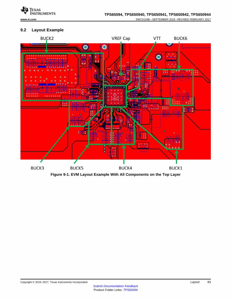
BUCK2
BUCK3 BUCK5 BUCK4 BUCK1
BUCK6VTTVREF Cap
83
TPS65094, TPS650940, TPS650941, TPS650942, TPS650944www.ti.com SWCS133B –SEPTEMBER 2015–REVISED FEBRUARY 2017
Submit Documentation FeedbackProduct Folder Links: TPS65094
LayoutCopyright © 2015–2017, Texas Instruments Incorporated
9.2 Layout Example
Figure 9-1. EVM Layout Example With All Components on the Top Layer
84
TPS65094, TPS650940, TPS650941, TPS650942, TPS650944SWCS133B –SEPTEMBER 2015–REVISED FEBRUARY 2017 www.ti.com
Submit Documentation FeedbackProduct Folder Links: TPS65094
Device and Documentation Support Copyright © 2015–2017, Texas Instruments Incorporated
10 Device and Documentation Support
10.1 Device Support
10.1.1 Third-Party Products DisclaimerTI'S PUBLICATION OF INFORMATION REGARDING THIRD-PARTY PRODUCTS OR SERVICES DOESNOT CONSTITUTE AN ENDORSEMENT REGARDING THE SUITABILITY OF SUCH PRODUCTS ORSERVICES OR A WARRANTY, REPRESENTATION OR ENDORSEMENT OF SUCH PRODUCTS ORSERVICES, EITHER ALONE OR IN COMBINATION WITH ANY TI PRODUCT OR SERVICE.
10.1.2 Development SupportSee the following for development support:
TPS65094x Schematic Checklist, Layout Checklist, and ILIM Calculator Tool
10.2 Documentation Support
10.2.1 Related DocumentationFor related documentation see the following:• TPS65094x Design Guide• TPS65094x Evaluation Module
10.3 Receiving Notification of Documentation UpdatesTo receive notification of documentation updates, navigate to the device product folder on ti.com. In theupper right corner, click on Alert me to register and receive a weekly digest of any product information thathas changed. For change details, review the revision history included in any revised document.
10.4 Community ResourcesThe following links connect to TI community resources. Linked contents are provided "AS IS" by therespective contributors. They do not constitute TI specifications and do not necessarily reflect TI's views;see TI's Terms of Use.TI E2E™ Online Community The TI engineer-to-engineer (E2E) community was created to foster
collaboration among engineers. At e2e.ti.com, you can ask questions, share knowledge,explore ideas and help solve problems with fellow engineers.
Design Support TI's Design Support Quickly find helpful E2E forums along with design support toolsand contact information for technical support.
10.5 TrademarksD-CAP2, D-CAP, E2E are trademarks of Texas Instruments.Ultrabook, Intel are trademarks of Intel Corporation.NXP is a trademark of NXP Semiconductors.All other trademarks are the property of their respective owners.
10.6 Electrostatic Discharge CautionThis integrated circuit can be damaged by ESD. Texas Instruments recommends that all integrated circuits be handled withappropriate precautions. Failure to observe proper handling and installation procedures can cause damage.
ESD damage can range from subtle performance degradation to complete device failure. Precision integrated circuits may be moresusceptible to damage because very small parametric changes could cause the device not to meet its published specifications.
10.7 GlossarySLYZ022 — TI Glossary.
This glossary lists and explains terms, acronyms, and definitions.
85
TPS65094, TPS650940, TPS650941, TPS650942, TPS650944www.ti.com SWCS133B –SEPTEMBER 2015–REVISED FEBRUARY 2017
Submit Documentation FeedbackProduct Folder Links: TPS65094
Mechanical, Packaging, and Orderable InformationCopyright © 2015–2017, Texas Instruments Incorporated
11 Mechanical, Packaging, and Orderable Information
The following pages include mechanical, packaging, and orderable information. This information is themost current data available for the designated devices. This data is subject to change without notice andrevision of this document. For browser-based versions of this data sheet, refer to the left-hand navigation.
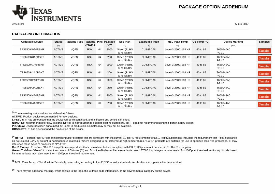
PACKAGE OPTION ADDENDUM
www.ti.com 5-Jun-2017
Addendum-Page 1
PACKAGING INFORMATION
Orderable Device Status(1)
Package Type PackageDrawing
Pins PackageQty
Eco Plan(2)
Lead/Ball Finish(6)
MSL Peak Temp(3)
Op Temp (°C) Device Marking(4/5)
Samples
TPS650940A0RSKR ACTIVE VQFN RSK 64 2000 Green (RoHS& no Sb/Br)
CU NIPDAU Level-3-260C-168 HR -40 to 85 T650940A0PG1.0
TPS650940A0RSKT ACTIVE VQFN RSK 64 250 Green (RoHS& no Sb/Br)
CU NIPDAU Level-3-260C-168 HR -40 to 85 T650940A0PG1.0
TPS650941A0RSKR ACTIVE VQFN RSK 64 2000 Green (RoHS& no Sb/Br)
CU NIPDAU Level-3-260C-168 HR -40 to 85 T650941A0PG1.0
TPS650941A0RSKT ACTIVE VQFN RSK 64 250 Green (RoHS& no Sb/Br)
CU NIPDAU Level-3-260C-168 HR -40 to 85 T650941A0PG1.0
TPS650942A0RSKR ACTIVE VQFN RSK 64 2000 Green (RoHS& no Sb/Br)
CU NIPDAU Level-3-260C-168 HR -40 to 85 T650942A0PG1.0
TPS650942A0RSKT ACTIVE VQFN RSK 64 250 Green (RoHS& no Sb/Br)
CU NIPDAU Level-3-260C-168 HR -40 to 85 T650942A0PG1.0
TPS650944A0RSKR ACTIVE VQFN RSK 64 2000 Green (RoHS& no Sb/Br)
CU NIPDAU Level-3-260C-168 HR -40 to 85 T650944A0PG1.0
TPS650944A0RSKT ACTIVE VQFN RSK 64 250 Green (RoHS& no Sb/Br)
CU NIPDAU Level-3-260C-168 HR -40 to 85 T650944A0PG1.0
(1) The marketing status values are defined as follows:ACTIVE: Product device recommended for new designs.LIFEBUY: TI has announced that the device will be discontinued, and a lifetime-buy period is in effect.NRND: Not recommended for new designs. Device is in production to support existing customers, but TI does not recommend using this part in a new design.PREVIEW: Device has been announced but is not in production. Samples may or may not be available.OBSOLETE: TI has discontinued the production of the device.
(2) RoHS: TI defines "RoHS" to mean semiconductor products that are compliant with the current EU RoHS requirements for all 10 RoHS substances, including the requirement that RoHS substancedo not exceed 0.1% by weight in homogeneous materials. Where designed to be soldered at high temperatures, "RoHS" products are suitable for use in specified lead-free processes. TI mayreference these types of products as "Pb-Free".RoHS Exempt: TI defines "RoHS Exempt" to mean products that contain lead but are compliant with EU RoHS pursuant to a specific EU RoHS exemption.Green: TI defines "Green" to mean the content of Chlorine (Cl) and Bromine (Br) based flame retardants meet JS709B low halogen requirements of <=1000ppm threshold. Antimony trioxide basedflame retardants must also meet the <=1000ppm threshold requirement.
(3) MSL, Peak Temp. - The Moisture Sensitivity Level rating according to the JEDEC industry standard classifications, and peak solder temperature.
(4) There may be additional marking, which relates to the logo, the lot trace code information, or the environmental category on the device.
PACKAGE OPTION ADDENDUM
www.ti.com 5-Jun-2017
Addendum-Page 2
(5) Multiple Device Markings will be inside parentheses. Only one Device Marking contained in parentheses and separated by a "~" will appear on a device. If a line is indented then it is a continuationof the previous line and the two combined represent the entire Device Marking for that device.
(6) Lead/Ball Finish - Orderable Devices may have multiple material finish options. Finish options are separated by a vertical ruled line. Lead/Ball Finish values may wrap to two lines if the finishvalue exceeds the maximum column width.
Important Information and Disclaimer:The information provided on this page represents TI's knowledge and belief as of the date that it is provided. TI bases its knowledge and belief on informationprovided by third parties, and makes no representation or warranty as to the accuracy of such information. Efforts are underway to better integrate information from third parties. TI has taken andcontinues to take reasonable steps to provide representative and accurate information but may not have conducted destructive testing or chemical analysis on incoming materials and chemicals.TI and TI suppliers consider certain information to be proprietary, and thus CAS numbers and other limited information may not be available for release.
In no event shall TI's liability arising out of such information exceed the total purchase price of the TI part(s) at issue in this document sold by TI to Customer on an annual basis.
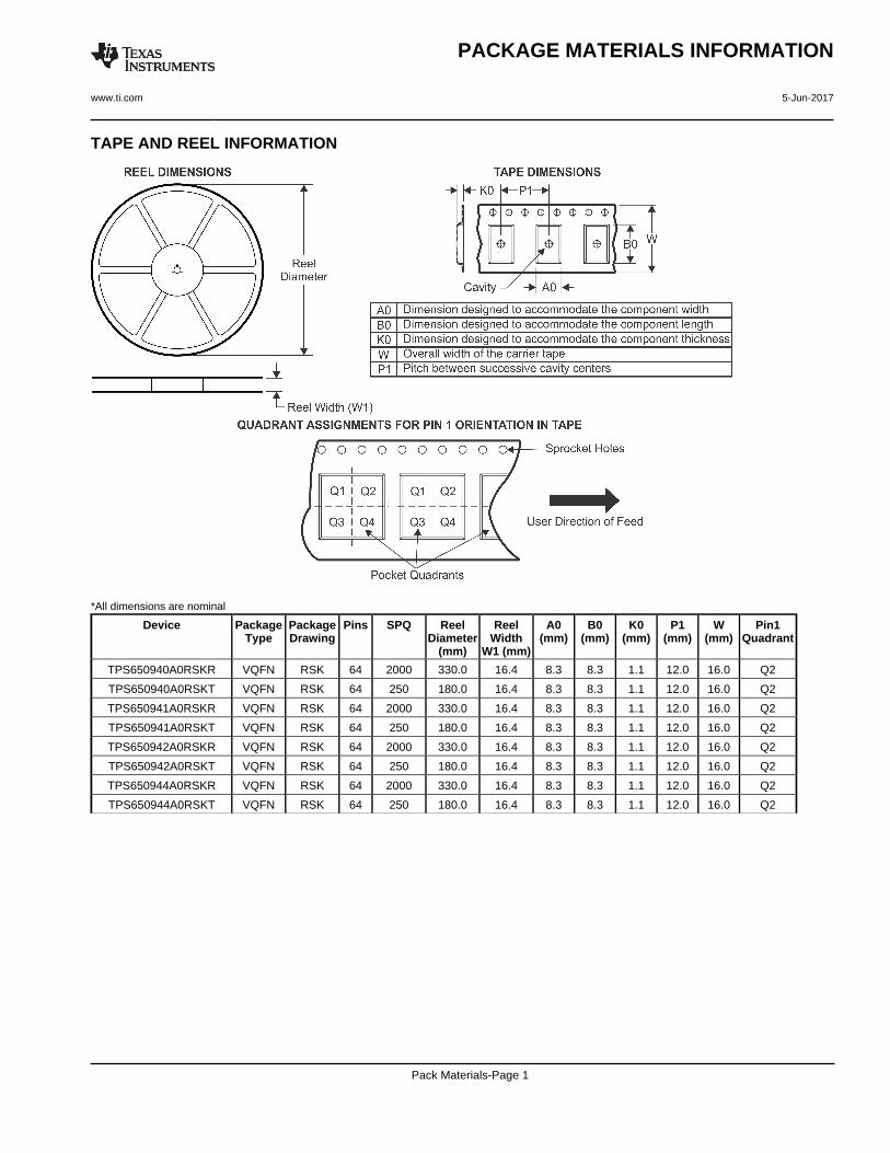
TAPE AND REEL INFORMATION
*All dimensions are nominal
Device PackageType
PackageDrawing
Pins SPQ ReelDiameter
(mm)
ReelWidth
W1 (mm)
A0(mm)
B0(mm)
K0(mm)
P1(mm)
W(mm)
Pin1Quadrant
TPS650940A0RSKR VQFN RSK 64 2000 330.0 16.4 8.3 8.3 1.1 12.0 16.0 Q2
TPS650940A0RSKT VQFN RSK 64 250 180.0 16.4 8.3 8.3 1.1 12.0 16.0 Q2
TPS650941A0RSKR VQFN RSK 64 2000 330.0 16.4 8.3 8.3 1.1 12.0 16.0 Q2
TPS650941A0RSKT VQFN RSK 64 250 180.0 16.4 8.3 8.3 1.1 12.0 16.0 Q2
TPS650942A0RSKR VQFN RSK 64 2000 330.0 16.4 8.3 8.3 1.1 12.0 16.0 Q2
TPS650942A0RSKT VQFN RSK 64 250 180.0 16.4 8.3 8.3 1.1 12.0 16.0 Q2
TPS650944A0RSKR VQFN RSK 64 2000 330.0 16.4 8.3 8.3 1.1 12.0 16.0 Q2
TPS650944A0RSKT VQFN RSK 64 250 180.0 16.4 8.3 8.3 1.1 12.0 16.0 Q2
PACKAGE MATERIALS INFORMATION
www.ti.com 5-Jun-2017
Pack Materials-Page 1
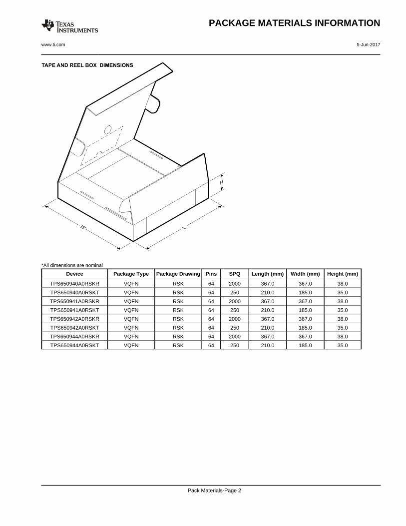
*All dimensions are nominal
Device Package Type Package Drawing Pins SPQ Length (mm) Width (mm) Height (mm)
TPS650940A0RSKR VQFN RSK 64 2000 367.0 367.0 38.0
TPS650940A0RSKT VQFN RSK 64 250 210.0 185.0 35.0
TPS650941A0RSKR VQFN RSK 64 2000 367.0 367.0 38.0
TPS650941A0RSKT VQFN RSK 64 250 210.0 185.0 35.0
TPS650942A0RSKR VQFN RSK 64 2000 367.0 367.0 38.0
TPS650942A0RSKT VQFN RSK 64 250 210.0 185.0 35.0
TPS650944A0RSKR VQFN RSK 64 2000 367.0 367.0 38.0
TPS650944A0RSKT VQFN RSK 64 250 210.0 185.0 35.0
PACKAGE MATERIALS INFORMATION
www.ti.com 5-Jun-2017
Pack Materials-Page 2
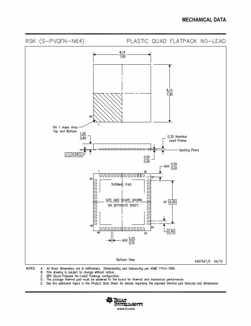
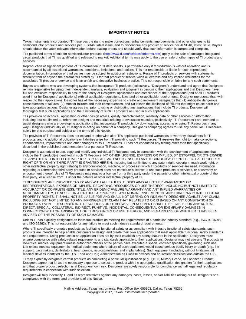
IMPORTANT NOTICE
Texas Instruments Incorporated (TI) reserves the right to make corrections, enhancements, improvements and other changes to itssemiconductor products and services per JESD46, latest issue, and to discontinue any product or service per JESD48, latest issue. Buyersshould obtain the latest relevant information before placing orders and should verify that such information is current and complete.TI’s published terms of sale for semiconductor products (http://www.ti.com/sc/docs/stdterms.htm) apply to the sale of packaged integratedcircuit products that TI has qualified and released to market. Additional terms may apply to the use or sale of other types of TI products andservices.Reproduction of significant portions of TI information in TI data sheets is permissible only if reproduction is without alteration and isaccompanied by all associated warranties, conditions, limitations, and notices. TI is not responsible or liable for such reproduceddocumentation. Information of third parties may be subject to additional restrictions. Resale of TI products or services with statementsdifferent from or beyond the parameters stated by TI for that product or service voids all express and any implied warranties for theassociated TI product or service and is an unfair and deceptive business practice. TI is not responsible or liable for any such statements.Buyers and others who are developing systems that incorporate TI products (collectively, “Designers”) understand and agree that Designersremain responsible for using their independent analysis, evaluation and judgment in designing their applications and that Designers havefull and exclusive responsibility to assure the safety of Designers' applications and compliance of their applications (and of all TI productsused in or for Designers’ applications) with all applicable regulations, laws and other applicable requirements. Designer represents that, withrespect to their applications, Designer has all the necessary expertise to create and implement safeguards that (1) anticipate dangerousconsequences of failures, (2) monitor failures and their consequences, and (3) lessen the likelihood of failures that might cause harm andtake appropriate actions. Designer agrees that prior to using or distributing any applications that include TI products, Designer willthoroughly test such applications and the functionality of such TI products as used in such applications.TI’s provision of technical, application or other design advice, quality characterization, reliability data or other services or information,including, but not limited to, reference designs and materials relating to evaluation modules, (collectively, “TI Resources”) are intended toassist designers who are developing applications that incorporate TI products; by downloading, accessing or using TI Resources in anyway, Designer (individually or, if Designer is acting on behalf of a company, Designer’s company) agrees to use any particular TI Resourcesolely for this purpose and subject to the terms of this Notice.TI’s provision of TI Resources does not expand or otherwise alter TI’s applicable published warranties or warranty disclaimers for TIproducts, and no additional obligations or liabilities arise from TI providing such TI Resources. TI reserves the right to make corrections,enhancements, improvements and other changes to its TI Resources. TI has not conducted any testing other than that specificallydescribed in the published documentation for a particular TI Resource.Designer is authorized to use, copy and modify any individual TI Resource only in connection with the development of applications thatinclude the TI product(s) identified in such TI Resource. NO OTHER LICENSE, EXPRESS OR IMPLIED, BY ESTOPPEL OR OTHERWISETO ANY OTHER TI INTELLECTUAL PROPERTY RIGHT, AND NO LICENSE TO ANY TECHNOLOGY OR INTELLECTUAL PROPERTYRIGHT OF TI OR ANY THIRD PARTY IS GRANTED HEREIN, including but not limited to any patent right, copyright, mask work right, orother intellectual property right relating to any combination, machine, or process in which TI products or services are used. Informationregarding or referencing third-party products or services does not constitute a license to use such products or services, or a warranty orendorsement thereof. Use of TI Resources may require a license from a third party under the patents or other intellectual property of thethird party, or a license from TI under the patents or other intellectual property of TI.TI RESOURCES ARE PROVIDED “AS IS” AND WITH ALL FAULTS. TI DISCLAIMS ALL OTHER WARRANTIES ORREPRESENTATIONS, EXPRESS OR IMPLIED, REGARDING RESOURCES OR USE THEREOF, INCLUDING BUT NOT LIMITED TOACCURACY OR COMPLETENESS, TITLE, ANY EPIDEMIC FAILURE WARRANTY AND ANY IMPLIED WARRANTIES OFMERCHANTABILITY, FITNESS FOR A PARTICULAR PURPOSE, AND NON-INFRINGEMENT OF ANY THIRD PARTY INTELLECTUALPROPERTY RIGHTS. TI SHALL NOT BE LIABLE FOR AND SHALL NOT DEFEND OR INDEMNIFY DESIGNER AGAINST ANY CLAIM,INCLUDING BUT NOT LIMITED TO ANY INFRINGEMENT CLAIM THAT RELATES TO OR IS BASED ON ANY COMBINATION OFPRODUCTS EVEN IF DESCRIBED IN TI RESOURCES OR OTHERWISE. IN NO EVENT SHALL TI BE LIABLE FOR ANY ACTUAL,DIRECT, SPECIAL, COLLATERAL, INDIRECT, PUNITIVE, INCIDENTAL, CONSEQUENTIAL OR EXEMPLARY DAMAGES INCONNECTION WITH OR ARISING OUT OF TI RESOURCES OR USE THEREOF, AND REGARDLESS OF WHETHER TI HAS BEENADVISED OF THE POSSIBILITY OF SUCH DAMAGES.Unless TI has explicitly designated an individual product as meeting the requirements of a particular industry standard (e.g., ISO/TS 16949and ISO 26262), TI is not responsible for any failure to meet such industry standard requirements.Where TI specifically promotes products as facilitating functional safety or as compliant with industry functional safety standards, suchproducts are intended to help enable customers to design and create their own applications that meet applicable functional safety standardsand requirements. Using products in an application does not by itself establish any safety features in the application. Designers mustensure compliance with safety-related requirements and standards applicable to their applications. Designer may not use any TI products inlife-critical medical equipment unless authorized officers of the parties have executed a special contract specifically governing such use.Life-critical medical equipment is medical equipment where failure of such equipment would cause serious bodily injury or death (e.g., lifesupport, pacemakers, defibrillators, heart pumps, neurostimulators, and implantables). Such equipment includes, without limitation, allmedical devices identified by the U.S. Food and Drug Administration as Class III devices and equivalent classifications outside the U.S.TI may expressly designate certain products as completing a particular qualification (e.g., Q100, Military Grade, or Enhanced Product).Designers agree that it has the necessary expertise to select the product with the appropriate qualification designation for their applicationsand that proper product selection is at Designers’ own risk. Designers are solely responsible for compliance with all legal and regulatoryrequirements in connection with such selection.Designer will fully indemnify TI and its representatives against any damages, costs, losses, and/or liabilities arising out of Designer’s non-compliance with the terms and provisions of this Notice.
Mailing Address: Texas Instruments, Post Office Box 655303, Dallas, Texas 75265Copyright © 2017, Texas Instruments Incorporated