Embed Size (px)
Citation preview
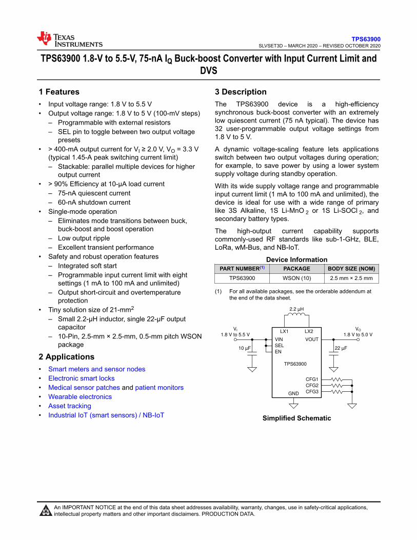
TPS63900 1.8-V to 5.5-V, 75-nA IQ Buck-boost Converter with Input Current Limit andDVS
1 Features• Input voltage range: 1.8 V to 5.5 V• Output voltage range: 1.8 V to 5 V (100-mV steps)
– Programmable with external resistors– SEL pin to toggle between two output voltage
presets• > 400-mA output current for VI ≥ 2.0 V, VO = 3.3 V
(typical 1.45-A peak switching current limit)– Stackable: parallel multiple devices for higher
output current• > 90% Efficiency at 10-µA load current
– 75-nA quiescent current– 60-nA shutdown current
• Single-mode operation– Eliminates mode transitions between buck,
buck-boost and boost operation– Low output ripple– Excellent transient performance
• Safety and robust operation features– Integrated soft start– Programmable input current limit with eight
settings (1 mA to 100 mA and unlimited)– Output short-circuit and overtemperature
protection• Tiny solution size of 21-mm2
– Small 2.2-µH inductor, single 22-µF outputcapacitor
– 10-Pin, 2.5-mm × 2.5-mm, 0.5-mm pitch WSONpackage
2 Applications• Smart meters and sensor nodes• Electronic smart locks• Medical sensor patches and patient monitors• Wearable electronics• Asset tracking• Industrial IoT (smart sensors) / NB-IoT
3 DescriptionThe TPS63900 device is a high-efficiencysynchronous buck-boost converter with an extremelylow quiescent current (75 nA typical). The device has32 user-programmable output voltage settings from1.8 V to 5 V.
A dynamic voltage-scaling feature lets applicationsswitch between two output voltages during operation;for example, to save power by using a lower systemsupply voltage during standby operation.
With its wide supply voltage range and programmableinput current limit (1 mA to 100 mA and unlimited), thedevice is ideal for use with a wide range of primarylike 3S Alkaline, 1S Li-MnO 2 or 1S Li-SOCl 2, andsecondary battery types.
The high-output current capability supportscommonly-used RF standards like sub-1-GHz, BLE,LoRa, wM-Bus, and NB-IoT.
Device InformationPART NUMBER(1) PACKAGE BODY SIZE (NOM)
TPS63900 WSON (10) 2.5 mm × 2.5 mm
(1) For all available packages, see the orderable addendum atthe end of the data sheet.
LX1 LX2
VIN VOUT
GND
VI
1.8 V to 5.5 VVO
1.8 V to 5.0 V
2.2 µH
CFG3
10 µF 22 µFSEL
EN
CFG2
CFG1
TPS63900
Simplified Schematic
www.ti.comTPS63900
SLVSET3D – MARCH 2020 – REVISED OCTOBER 2020
Copyright © 2020 Texas Instruments Incorporated Submit Document Feedback 1
Product Folder Links: TPS63900
TPS63900SLVSET3D – MARCH 2020 – REVISED OCTOBER 2020
An IMPORTANT NOTICE at the end of this data sheet addresses availability, warranty, changes, use in safety-critical applications,intellectual property matters and other important disclaimers. PRODUCTION DATA.
Table of Contents1 Features............................................................................12 Applications..................................................................... 13 Description.......................................................................14 Revision History.............................................................. 25 Pin Configuration and Functions...................................36 Specifications.................................................................. 4
6.1 Absolute Maximum Ratings ....................................... 46.2 ESD Ratings .............................................................. 46.3 Recommended Operating Conditions ........................46.4 Thermal Information ...................................................46.5 Electrical Characteristics ............................................56.6 Typical Characteristics................................................ 7
7 Detailed Description........................................................87.1 Overview..................................................................... 87.2 Functional Block Diagram........................................... 87.3 Feature Description.....................................................87.4 Device Functional Modes..........................................17
8 Application and Implementation.................................. 188.1 Application Information............................................. 188.2 Typical Application.................................................... 18
9 Power Supply Recommendations................................3010 Layout...........................................................................31
10.1 Layout Guidelines................................................... 3110.2 Layout Example...................................................... 31
11 Device and Documentation Support..........................3211.1 Device Support........................................................3211.2 Documentation Support.......................................... 3211.3 Receiving Notification of Documentation Updates.. 3211.4 Support Resources................................................. 3211.5 Trademarks............................................................. 3211.6 Electrostatic Discharge Caution.............................. 3211.7 Glossary.................................................................. 32
12 Mechanical, Packaging, and OrderableInformation.................................................................... 32
4 Revision HistoryNOTE: Page numbers for previous revisions may differ from page numbers in the current version.
Changes from Revision C (September 2020) to Revision D (October 2020) Page• Changed device status from Advance Information to Production Data.............................................................. 1
TPS63900SLVSET3D – MARCH 2020 – REVISED OCTOBER 2020 www.ti.com
2 Submit Document Feedback Copyright © 2020 Texas Instruments Incorporated
Product Folder Links: TPS63900
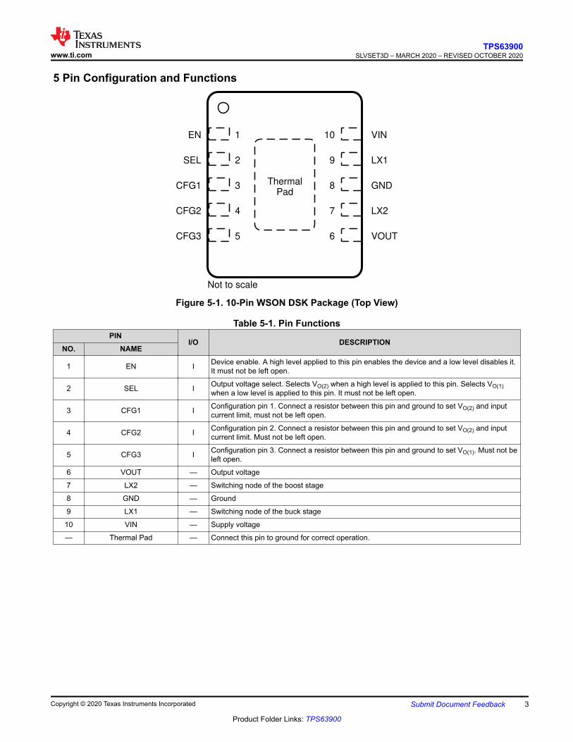
5 Pin Configuration and Functions
1EN 10 VIN
2SEL 9 LX1
3CFG1 8 GND
4CFG2 7 LX2
5CFG3 6 VOUT
Not to scale
Thermal
Pad
Figure 5-1. 10-Pin WSON DSK Package (Top View)
Table 5-1. Pin FunctionsPIN
I/O DESCRIPTIONNO. NAME
1 EN I Device enable. A high level applied to this pin enables the device and a low level disables it.It must not be left open.
2 SEL I Output voltage select. Selects VO(2) when a high level is applied to this pin. Selects VO(1)when a low level is applied to this pin. It must not be left open.
3 CFG1 I Configuration pin 1. Connect a resistor between this pin and ground to set VO(2) and inputcurrent limit, must not be left open.
4 CFG2 I Configuration pin 2. Connect a resistor between this pin and ground to set VO(2) and inputcurrent limit. Must not be left open.
5 CFG3 I Configuration pin 3. Connect a resistor between this pin and ground to set VO(1). Must not beleft open.
6 VOUT — Output voltage
7 LX2 — Switching node of the boost stage
8 GND — Ground
9 LX1 — Switching node of the buck stage
10 VIN — Supply voltage
— Thermal Pad — Connect this pin to ground for correct operation.
www.ti.comTPS63900
SLVSET3D – MARCH 2020 – REVISED OCTOBER 2020
Copyright © 2020 Texas Instruments Incorporated Submit Document Feedback 3
Product Folder Links: TPS63900
6 Specifications
6.1 Absolute Maximum Ratingsover operating junction temperature range (unless otherwise noted)(1)
MIN MAX UNITVI Input voltage (VIN, LX1, LX2, VOUT, EN, CFG1, CFG2, CFG3, SEL)(2) –0.3 5.9 V
TJ Operating junction temperature –40 150 °C
Tstg Storage temperature –65 150 °C
(1) Stresses beyond those listed under Absolute Maximum Ratings may cause permanent damage to the device. These are stress ratingsonly, which do not imply functional operation of the device at these or any other conditions beyond those indicated underRecommended Operating Conditions. Exposure to absolute-maximum-rated conditions for extended periods may affect devicereliability.
(2) All voltage values are with respect to network ground terminal, unless otherwise noted.
6.2 ESD RatingsVALUE UNIT
V(ESD) Electrostatic dischargeHuman body model (HBM), per ANSI/ESDA/JEDEC JS-001(1) ±2000
VCharged-device model (CDM), per JEDEC specification JESD22-C101or ANSI/ESDA/JEDEC JS-002(2) ±750
(1) JEDEC document JEP155 states that 500-V HBM allows safe manufacturing with a standard ESD control process.(2) JEDEC document JEP157 states that 250-V CDM allows safe manufacturing with a standard ESD control process.
6.3 Recommended Operating Conditionsover operating free-air temperature range (unless otherwise noted)
MIN NOM MAX UNITVI Supply voltage 1.8 5.5 V
VO Output voltage 1.8 5.0 V
IO Output current (VI ≥ 2.0 V, VO = 3.6 V) 0.4 A
CI Input capacitance (VI = 2.5 V to 5 V, VO = 3.3 V, IO = 0.4 A)(1) 5 µF
CO Output capacitance (VI = 2.5 V to 5 V, VO = 3.3 V, IO = 0.4 A)(1) 10 µF
C(CFG) Capacitance (CFG1, CFG2, CFG3) 10 pF
L Inductance 2.2 µH
ISAT Inductor saturation current ratingUnlimited current setting 2
A≤100-mA current settings 1
TA Operating ambient temperature –40 85 °C
TJ Operating junction temperature –40 125 °C
(1) Effective capacitance after DC bias effects have been considered.
6.4 Thermal Information
THERMAL METRIC(1)
TPS63900
UNITDSK Package(WSON)10 PINS
RθJA Junction-to-ambient thermal resistance 64.6 °C/W
RθJC(top) Junction-to-case (top) thermal resistance 62.3 °C/W
RθJB Junction-to-board thermal resistance 31.1 °C/W
ψJT Junction-to-top characterization parameter 1.6 °C/W
TPS63900SLVSET3D – MARCH 2020 – REVISED OCTOBER 2020 www.ti.com
4 Submit Document Feedback Copyright © 2020 Texas Instruments Incorporated
Product Folder Links: TPS63900
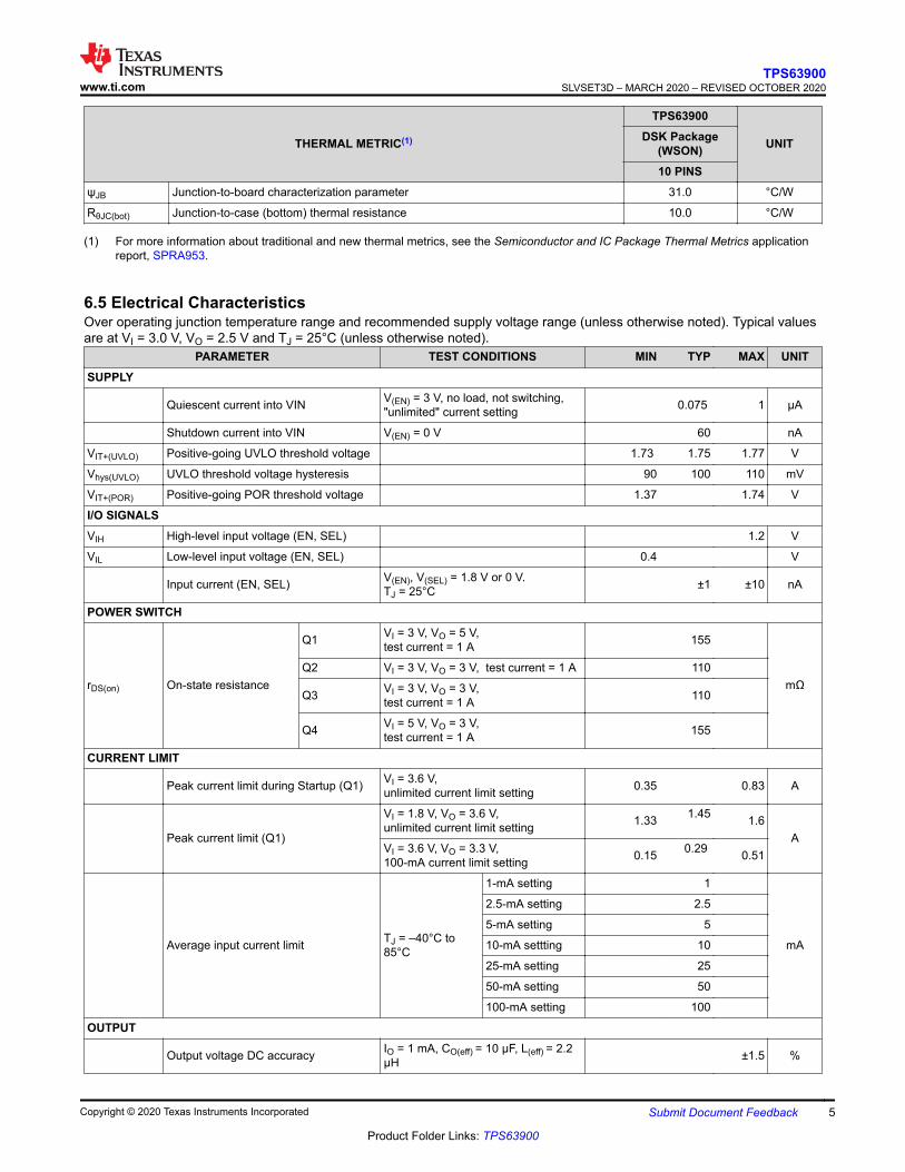
THERMAL METRIC(1)
TPS63900
UNITDSK Package(WSON)10 PINS
ψJB Junction-to-board characterization parameter 31.0 °C/W
RθJC(bot) Junction-to-case (bottom) thermal resistance 10.0 °C/W
(1) For more information about traditional and new thermal metrics, see the Semiconductor and IC Package Thermal Metrics applicationreport, SPRA953.
6.5 Electrical CharacteristicsOver operating junction temperature range and recommended supply voltage range (unless otherwise noted). Typical valuesare at VI = 3.0 V, VO = 2.5 V and TJ = 25°C (unless otherwise noted).
PARAMETER TEST CONDITIONS MIN TYP MAX UNITSUPPLY
Quiescent current into VIN V(EN) = 3 V, no load, not switching,"unlimited" current setting 0.075 1 µA
Shutdown current into VIN V(EN) = 0 V 60 nA
VIT+(UVLO) Positive-going UVLO threshold voltage 1.73 1.75 1.77 V
Vhys(UVLO) UVLO threshold voltage hysteresis 90 100 110 mV
VIT+(POR) Positive-going POR threshold voltage 1.37 1.74 V
I/O SIGNALSVIH High-level input voltage (EN, SEL) 1.2 V
VIL Low-level input voltage (EN, SEL) 0.4 V
Input current (EN, SEL) V(EN), V(SEL) = 1.8 V or 0 V.TJ = 25°C ±1 ±10 nA
POWER SWITCH
rDS(on) On-state resistance
Q1 VI = 3 V, VO = 5 V, test current = 1 A 155
mΩQ2 VI = 3 V, VO = 3 V, test current = 1 A 110
Q3 VI = 3 V, VO = 3 V, test current = 1 A 110
Q4 VI = 5 V, VO = 3 V, test current = 1 A 155
CURRENT LIMIT
Peak current limit during Startup (Q1) VI = 3.6 V,unlimited current limit setting 0.35 0.83 A
Peak current limit (Q1)
VI = 1.8 V, VO = 3.6 V,unlimited current limit setting 1.33 1.45
1.6A
VI = 3.6 V, VO = 3.3 V,100-mA current limit setting 0.15 0.29
0.51
Average input current limit TJ = –40°C to85°C
1-mA setting 1
mA
2.5-mA setting 2.5
5-mA setting 5
10-mA settting 10
25-mA setting 25
50-mA setting 50
100-mA setting 100
OUTPUT
Output voltage DC accuracy IO = 1 mA, CO(eff) = 10 µF, L(eff) = 2.2µH ±1.5 %
www.ti.comTPS63900
SLVSET3D – MARCH 2020 – REVISED OCTOBER 2020
Copyright © 2020 Texas Instruments Incorporated Submit Document Feedback 5
Product Folder Links: TPS63900
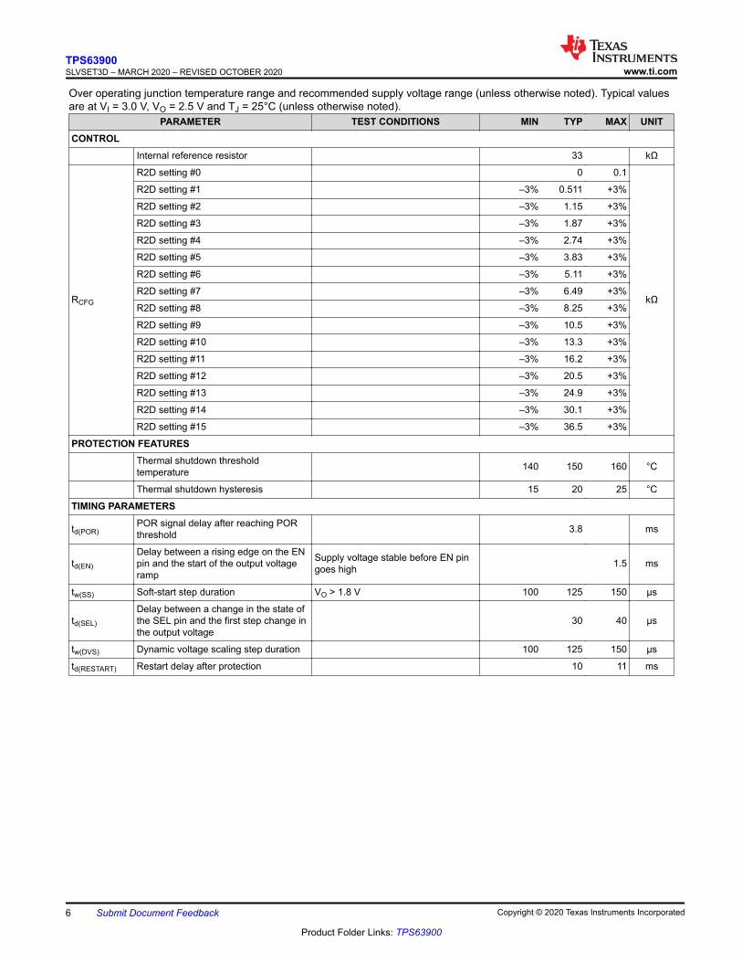
Over operating junction temperature range and recommended supply voltage range (unless otherwise noted). Typical valuesare at VI = 3.0 V, VO = 2.5 V and TJ = 25°C (unless otherwise noted).
PARAMETER TEST CONDITIONS MIN TYP MAX UNITCONTROL
Internal reference resistor 33 kΩ
RCFG
R2D setting #0 0 0.1
kΩ
R2D setting #1 –3% 0.511 +3%
R2D setting #2 –3% 1.15 +3%
R2D setting #3 –3% 1.87 +3%
R2D setting #4 –3% 2.74 +3%
R2D setting #5 –3% 3.83 +3%
R2D setting #6 –3% 5.11 +3%
R2D setting #7 –3% 6.49 +3%
R2D setting #8 –3% 8.25 +3%
R2D setting #9 –3% 10.5 +3%
R2D setting #10 –3% 13.3 +3%
R2D setting #11 –3% 16.2 +3%
R2D setting #12 –3% 20.5 +3%
R2D setting #13 –3% 24.9 +3%
R2D setting #14 –3% 30.1 +3%
R2D setting #15 –3% 36.5 +3%
PROTECTION FEATURESThermal shutdown thresholdtemperature 140 150 160 °C
Thermal shutdown hysteresis 15 20 25 °C
TIMING PARAMETERS
td(POR)POR signal delay after reaching PORthreshold 3.8 ms
td(EN)
Delay between a rising edge on the ENpin and the start of the output voltageramp
Supply voltage stable before EN pingoes high 1.5 ms
tw(SS) Soft-start step duration VO > 1.8 V 100 125 150 µs
td(SEL)
Delay between a change in the state ofthe SEL pin and the first step change inthe output voltage
30 40 µs
tw(DVS) Dynamic voltage scaling step duration 100 125 150 µs
td(RESTART) Restart delay after protection 10 11 ms
TPS63900SLVSET3D – MARCH 2020 – REVISED OCTOBER 2020 www.ti.com
6 Submit Document Feedback Copyright © 2020 Texas Instruments Incorporated
Product Folder Links: TPS63900
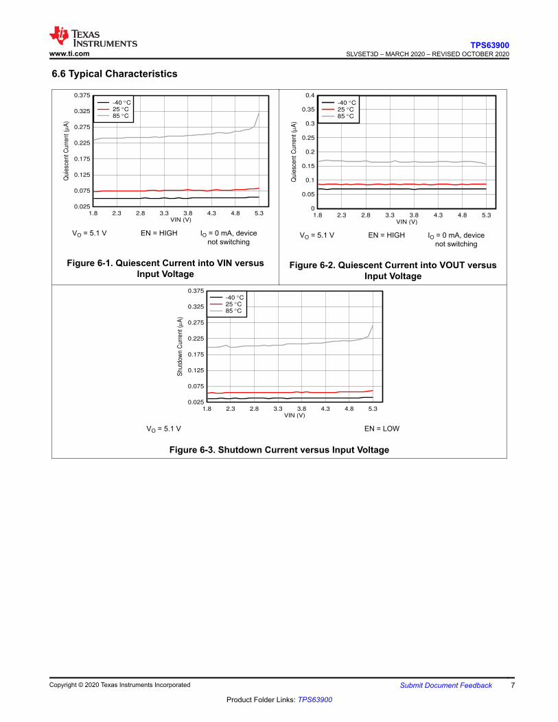
6.6 Typical Characteristics
VIN (V)
Qu
iesc
en
t C
urr
ent
(PA
)
1.8 2.3 2.8 3.3 3.8 4.3 4.8 5.30.025
0.075
0.125
0.175
0.225
0.275
0.325
0.375
-40 qC25 qC85 qC
VO = 5.1 V EN = HIGH IO = 0 mA, devicenot switching
Figure 6-1. Quiescent Current into VIN versusInput Voltage
VIN (V)
Qu
iesc
en
t C
urr
ent
(PA
)
1.8 2.3 2.8 3.3 3.8 4.3 4.8 5.30
0.05
0.1
0.15
0.2
0.25
0.3
0.35
0.4
-40 qC25 qC85 qC
VO = 5.1 V EN = HIGH IO = 0 mA, devicenot switching
Figure 6-2. Quiescent Current into VOUT versusInput Voltage
VIN (V)
Sh
utd
ow
n C
urr
ent
(PA
)
1.8 2.3 2.8 3.3 3.8 4.3 4.8 5.30.025
0.075
0.125
0.175
0.225
0.275
0.325
0.375-40 qC25 qC85 qC
VO = 5.1 V EN = LOW
Figure 6-3. Shutdown Current versus Input Voltage
www.ti.comTPS63900
SLVSET3D – MARCH 2020 – REVISED OCTOBER 2020
Copyright © 2020 Texas Instruments Incorporated Submit Document Feedback 7
Product Folder Links: TPS63900
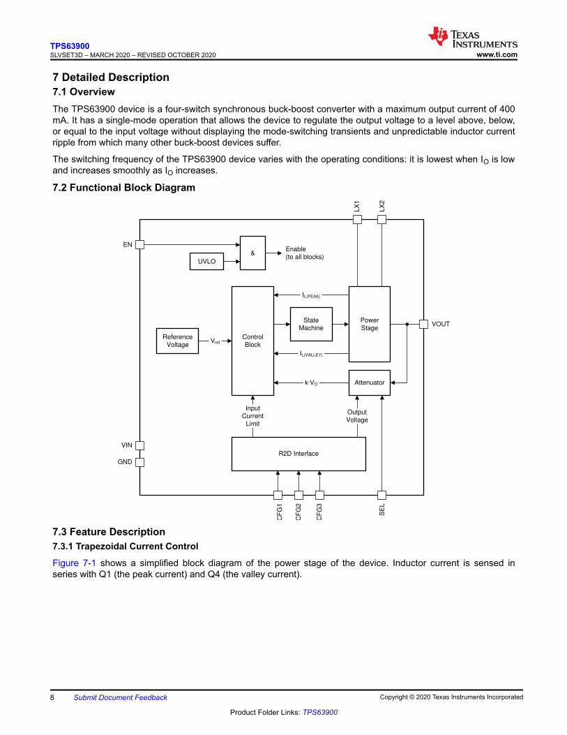
7 Detailed Description7.1 OverviewThe TPS63900 device is a four-switch synchronous buck-boost converter with a maximum output current of 400mA. It has a single-mode operation that allows the device to regulate the output voltage to a level above, below,or equal to the input voltage without displaying the mode-switching transients and unpredictable inductor currentripple from which many other buck-boost devices suffer.
The switching frequency of the TPS63900 device varies with the operating conditions: it is lowest when IO is lowand increases smoothly as IO increases.
7.2 Functional Block Diagram
UVLO
Reference
Voltage
R2D Interface
Control
BlocktVreft
VIN
LX
2
LX
1
EN
SE
L
CF
G1
CF
G2
CF
G3
&Enable
(to all blocks)
State
MachineVOUT
tIL(PEAK)t
Attenuator
Power
Stage
Input
Current
Limit
Output
Voltage
GND
tNÂ9Ot
tIL(VALLEY)t
7.3 Feature Description7.3.1 Trapezoidal Current Control
Figure 7-1 shows a simplified block diagram of the power stage of the device. Inductor current is sensed inseries with Q1 (the peak current) and Q4 (the valley current).
TPS63900SLVSET3D – MARCH 2020 – REVISED OCTOBER 2020 www.ti.com
8 Submit Document Feedback Copyright © 2020 Texas Instruments Incorporated
Product Folder Links: TPS63900
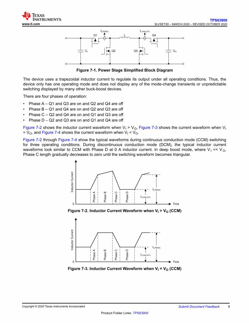
LQ1 Q4
Q2 Q3CI CO
IL(PEAK) IL(VALLEY)
Figure 7-1. Power Stage Simplified Block Diagram
The device uses a trapezoidal inductor current to regulate its output under all operating conditions. Thus, thedevice only has one operating mode and does not display any of the mode-change transients or unpredictableswitching displayed by many other buck-boost devices.
There are four phases of operation:
• Phase A – Q1 and Q3 are on and Q2 and Q4 are off• Phase B – Q1 and Q4 are on and Q2 and Q3 are off• Phase C – Q2 and Q4 are on and Q1 and Q3 are off• Phase D – Q2 and Q3 are on and Q1 and Q4 are off
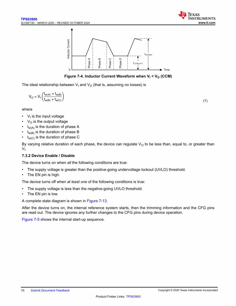
Figure 7-2 shows the inductor current waveform when VI > VO, Figure 7-3 shows the current waveform when VI= VO, and Figure 7-4 shows the current waveform when VI < VO.
Figure 7-2 through Figure 7-4 show the typical waveforms during continuous conduction mode (CCM) switchingfor three operating conditions. During discontinuous conduction mode (DCM), the typical inductor currentwaveforms look similar to CCM with Phase D at 0 A inductor current. In deep boost mode, where V I << V O,Phase C length gradually decreases to zero until the switching waveform becomes triangular.
Ind
ucto
r C
urr
en
t
Time0
IL(VALLEY)
IL(PEAK)
Ph
ase
A
Ph
ase
B
Ph
ase
D
Ph
ase
C
Figure 7-2. Inductor Current Waveform when VI > VO (CCM)
Ind
ucto
r C
urr
en
t
Time0
IL(VALLEY)
IL(PEAK)
Ph
ase
A
Ph
ase
B
Ph
ase
D
Ph
ase
C
Figure 7-3. Inductor Current Waveform when VI = VO (CCM)
www.ti.comTPS63900
SLVSET3D – MARCH 2020 – REVISED OCTOBER 2020
Copyright © 2020 Texas Instruments Incorporated Submit Document Feedback 9
Product Folder Links: TPS63900
Ind
ucto
r C
urr
en
tTime0
IL(VALLEY)
IL(PEAK)
Ph
ase
A
Ph
ase
B
Ph
ase
D
Ph
ase
C
Figure 7-4. Inductor Current Waveform when VI < VO (CCM)
The ideal relationship between VI and VO (that is, assuming no losses) is
VO = VI Ftw:A; + tw(B)
tw(B) + tw(C)
G (1)
where
• VI is the input voltage• VO is the output voltage• tw(A) is the duration of phase A• tw(B) is the duration of phase B• tw(C) is the duration of phase C
By varying relative duration of each phase, the device can regulate VO to be less than, equal to, or greater thanVI.
7.3.2 Device Enable / Disable
The device turns on when all the following conditions are true:
• The supply voltage is greater than the positive-going undervoltage lockout (UVLO) threshold.• The EN pin is high.
The device turns off when at least one of the following conditions is true:
• The supply voltage is less than the negative-going UVLO threshold.• The EN pin is low.
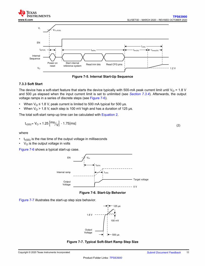
A complete state diagram is shown in Figure 7-13.
After the device turns on, the internal reference system starts, then the trimming information and the CFG pinsare read out. The device ignores any further changes to the CFG pins during device operation.
Figure 7-5 shows the internal start-up sequence.
TPS63900SLVSET3D – MARCH 2020 – REVISED OCTOBER 2020 www.ti.com
10 Submit Document Feedback Copyright © 2020 Texas Instruments Incorporated
Product Folder Links: TPS63900
EN
Internal
Sequence
ttd(EN)t
VI
Start internal
reference systemRead trim bits Read CFG pins
VO
VIT+(POR)
Power-on
reset
td(POR)
1.2 V
ttlim(SS)t ttramp(SS)t
ttr(SS)t
Figure 7-5. Internal Start-Up Sequence
7.3.3 Soft Start
The device has a soft-start feature that starts the device typically with 500-mA peak current limit until VO = 1.8 Vand 500 µs elapsed when the input current limit is set to unlimited (see Section 7.3.4). Afterwards, the outputvoltage ramps in a series of discrete steps (see Figure 7-6).
• When VO ≤ 1.8 V, peak current is limited to 500 mA typical for 500 µs.• When VO > 1.8 V, each step is 100 mV high and has a duration of 125 µs.
The total soft-start ramp-up time can be calculated with Equation 2.
tr(SS)= VO × 1.25 BmsVW C - 1.75>ms? (2)
where
• tr(SS) is the rise time of the output voltage in milliseconds• VO is the output voltage in volts
Figure 7-6 shows a typical start-up case.
EN
ttr(SS)t
VIH
Output
Voltage
Target voltage
Internal ramp
ttd(EN)t
0 V
Figure 7-6. Start-Up Behavior
Figure 7-7 illustrates the start-up step size behavior.
OutputVoltage
1.8 V
t100 mVt
t125 µst
t500 µst
Figure 7-7. Typical Soft-Start Ramp Step Size
www.ti.comTPS63900
SLVSET3D – MARCH 2020 – REVISED OCTOBER 2020
Copyright © 2020 Texas Instruments Incorporated Submit Document Feedback 11
Product Folder Links: TPS63900
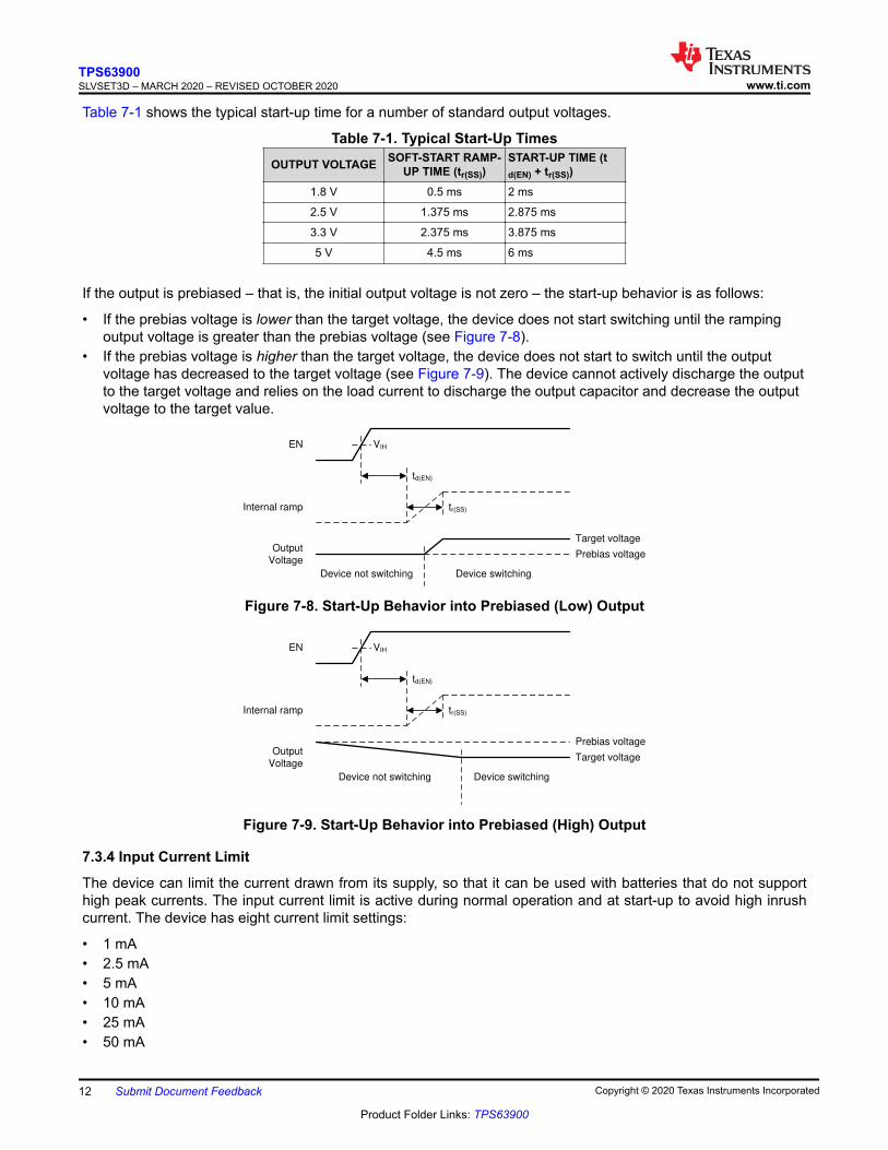
Table 7-1 shows the typical start-up time for a number of standard output voltages.
Table 7-1. Typical Start-Up TimesOUTPUT VOLTAGE SOFT-START RAMP-
UP TIME (tr(SS))START-UP TIME (td(EN) + tr(SS))
1.8 V 0.5 ms 2 ms
2.5 V 1.375 ms 2.875 ms
3.3 V 2.375 ms 3.875 ms
5 V 4.5 ms 6 ms
If the output is prebiased – that is, the initial output voltage is not zero – the start-up behavior is as follows:
• If the prebias voltage is lower than the target voltage, the device does not start switching until the rampingoutput voltage is greater than the prebias voltage (see Figure 7-8).
• If the prebias voltage is higher than the target voltage, the device does not start to switch until the outputvoltage has decreased to the target voltage (see Figure 7-9). The device cannot actively discharge the outputto the target voltage and relies on the load current to discharge the output capacitor and decrease the outputvoltage to the target value.
EN
ttr(SS)t
VIH
Output
VoltagePrebias voltage
Target voltage
Device switching
Internal ramp
ttd(EN)t
Device not switching
Figure 7-8. Start-Up Behavior into Prebiased (Low) Output
EN
ttr(SS)t
VIH
Output
Voltage
Prebias voltage
Target voltage
Device switching
Internal ramp
ttd(EN)t
Device not switching
Figure 7-9. Start-Up Behavior into Prebiased (High) Output
7.3.4 Input Current Limit
The device can limit the current drawn from its supply, so that it can be used with batteries that do not supporthigh peak currents. The input current limit is active during normal operation and at start-up to avoid high inrushcurrent. The device has eight current limit settings:
• 1 mA• 2.5 mA• 5 mA• 10 mA• 25 mA• 50 mA
TPS63900SLVSET3D – MARCH 2020 – REVISED OCTOBER 2020 www.ti.com
12 Submit Document Feedback Copyright © 2020 Texas Instruments Incorporated
Product Folder Links: TPS63900
• 100 mA• Unlimited
CFG1 and CFG2 pins select which setting is active (see Section 7.3.6).
7.3.5 Dynamic Voltage Scaling
The device has a dynamic voltage scaling function to switch between the two output voltage settings. When theSEL pin changes state, the output voltage ramps to the new value in 100-mV steps. The duration of each step is125 µs (see Figure 7-10).
The device does not actively discharge the output capacitor, when the output voltage ramps to a lower level.This leads to a longer output voltage settling time when light load is applied (see Figure 7-11). The settling timecan be calculated with Equation 3.
tsettle= CO × VO(HIGH) F VO(LOW)
IO
(3)
SEL
Output
Voltage
VO(1)
VO(2)
ttw(DVS)tt100 mVt
ttd(SEL)t
Figure 7-10. Dynamic Voltage Scaling with HighLoad
SEL
Output
Voltage
VO(1)
VO(2)
ttw(DVS)t
ttd(SEL)t
Figure 7-11. Dynamic Voltage Scaling with LightLoad
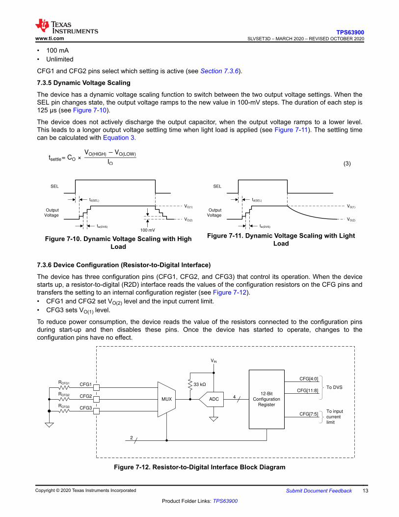
7.3.6 Device Configuration (Resistor-to-Digital Interface)
The device has three configuration pins (CFG1, CFG2, and CFG3) that control its operation. When the devicestarts up, a resistor-to-digital (R2D) interface reads the values of the configuration resistors on the CFG pins andtransfers the setting to an internal configuration register (see Figure 7-12).• CFG1 and CFG2 set VO(2) level and the input current limit.• CFG3 sets VO(1) level.
To reduce power consumption, the device reads the value of the resistors connected to the configuration pinsduring start-up and then disables these pins. Once the device has started to operate, changes to theconfiguration pins have no effect.
ADC4
VIN
33 N
MUX
CFG1
CFG2
CFG3
12-Bit
Configuration
Register
CFG[7:5]
RCFG1
RCFG2
RCFG3
CFG[11:8]
CFG[4:0]
To DVS
To input
current
limit
2
Figure 7-12. Resistor-to-Digital Interface Block Diagram
www.ti.comTPS63900
SLVSET3D – MARCH 2020 – REVISED OCTOBER 2020
Copyright © 2020 Texas Instruments Incorporated Submit Document Feedback 13
Product Folder Links: TPS63900
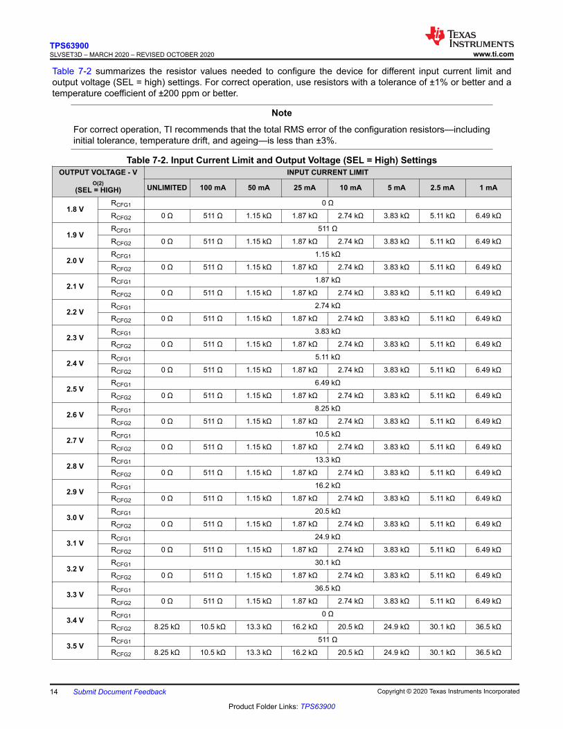
Table 7-2 summarizes the resistor values needed to configure the device for different input current limit andoutput voltage (SEL = high) settings. For correct operation, use resistors with a tolerance of ±1% or better and atemperature coefficient of ±200 ppm or better.
Note
For correct operation, TI recommends that the total RMS error of the configuration resistors—includinginitial tolerance, temperature drift, and ageing—is less than ±3%.
Table 7-2. Input Current Limit and Output Voltage (SEL = High) SettingsOUTPUT VOLTAGE - V
O(2)(SEL = HIGH)
INPUT CURRENT LIMIT
UNLIMITED 100 mA 50 mA 25 mA 10 mA 5 mA 2.5 mA 1 mA
1.8 VRCFG1 0 Ω
RCFG2 0 Ω 511 Ω 1.15 kΩ 1.87 kΩ 2.74 kΩ 3.83 kΩ 5.11 kΩ 6.49 kΩ
1.9 VRCFG1 511 Ω
RCFG2 0 Ω 511 Ω 1.15 kΩ 1.87 kΩ 2.74 kΩ 3.83 kΩ 5.11 kΩ 6.49 kΩ
2.0 VRCFG1 1.15 kΩ
RCFG2 0 Ω 511 Ω 1.15 kΩ 1.87 kΩ 2.74 kΩ 3.83 kΩ 5.11 kΩ 6.49 kΩ
2.1 VRCFG1 1.87 kΩ
RCFG2 0 Ω 511 Ω 1.15 kΩ 1.87 kΩ 2.74 kΩ 3.83 kΩ 5.11 kΩ 6.49 kΩ
2.2 VRCFG1 2.74 kΩ
RCFG2 0 Ω 511 Ω 1.15 kΩ 1.87 kΩ 2.74 kΩ 3.83 kΩ 5.11 kΩ 6.49 kΩ
2.3 VRCFG1 3.83 kΩ
RCFG2 0 Ω 511 Ω 1.15 kΩ 1.87 kΩ 2.74 kΩ 3.83 kΩ 5.11 kΩ 6.49 kΩ
2.4 VRCFG1 5.11 kΩ
RCFG2 0 Ω 511 Ω 1.15 kΩ 1.87 kΩ 2.74 kΩ 3.83 kΩ 5.11 kΩ 6.49 kΩ
2.5 VRCFG1 6.49 kΩ
RCFG2 0 Ω 511 Ω 1.15 kΩ 1.87 kΩ 2.74 kΩ 3.83 kΩ 5.11 kΩ 6.49 kΩ
2.6 VRCFG1 8.25 kΩ
RCFG2 0 Ω 511 Ω 1.15 kΩ 1.87 kΩ 2.74 kΩ 3.83 kΩ 5.11 kΩ 6.49 kΩ
2.7 VRCFG1 10.5 kΩ
RCFG2 0 Ω 511 Ω 1.15 kΩ 1.87 kΩ 2.74 kΩ 3.83 kΩ 5.11 kΩ 6.49 kΩ
2.8 VRCFG1 13.3 kΩ
RCFG2 0 Ω 511 Ω 1.15 kΩ 1.87 kΩ 2.74 kΩ 3.83 kΩ 5.11 kΩ 6.49 kΩ
2.9 VRCFG1 16.2 kΩ
RCFG2 0 Ω 511 Ω 1.15 kΩ 1.87 kΩ 2.74 kΩ 3.83 kΩ 5.11 kΩ 6.49 kΩ
3.0 VRCFG1 20.5 kΩ
RCFG2 0 Ω 511 Ω 1.15 kΩ 1.87 kΩ 2.74 kΩ 3.83 kΩ 5.11 kΩ 6.49 kΩ
3.1 VRCFG1 24.9 kΩ
RCFG2 0 Ω 511 Ω 1.15 kΩ 1.87 kΩ 2.74 kΩ 3.83 kΩ 5.11 kΩ 6.49 kΩ
3.2 VRCFG1 30.1 kΩ
RCFG2 0 Ω 511 Ω 1.15 kΩ 1.87 kΩ 2.74 kΩ 3.83 kΩ 5.11 kΩ 6.49 kΩ
3.3 VRCFG1 36.5 kΩ
RCFG2 0 Ω 511 Ω 1.15 kΩ 1.87 kΩ 2.74 kΩ 3.83 kΩ 5.11 kΩ 6.49 kΩ
3.4 VRCFG1 0 Ω
RCFG2 8.25 kΩ 10.5 kΩ 13.3 kΩ 16.2 kΩ 20.5 kΩ 24.9 kΩ 30.1 kΩ 36.5 kΩ
3.5 VRCFG1 511 Ω
RCFG2 8.25 kΩ 10.5 kΩ 13.3 kΩ 16.2 kΩ 20.5 kΩ 24.9 kΩ 30.1 kΩ 36.5 kΩ
TPS63900SLVSET3D – MARCH 2020 – REVISED OCTOBER 2020 www.ti.com
14 Submit Document Feedback Copyright © 2020 Texas Instruments Incorporated
Product Folder Links: TPS63900
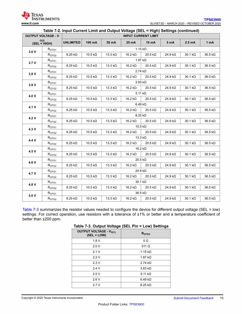
Table 7-2. Input Current Limit and Output Voltage (SEL = High) Settings (continued)OUTPUT VOLTAGE - V
O(2)(SEL = HIGH)
INPUT CURRENT LIMIT
UNLIMITED 100 mA 50 mA 25 mA 10 mA 5 mA 2.5 mA 1 mA
3.6 VRCFG1 1.15 kΩ
RCFG2 8.25 kΩ 10.5 kΩ 13.3 kΩ 16.2 kΩ 20.5 kΩ 24.9 kΩ 30.1 kΩ 36.5 kΩ
3.7 VRCFG1 1.87 kΩ
RCFG2 8.25 kΩ 10.5 kΩ 13.3 kΩ 16.2 kΩ 20.5 kΩ 24.9 kΩ 30.1 kΩ 36.5 kΩ
3.8 VRCFG1 2.74 kΩ
RCFG2 8.25 kΩ 10.5 kΩ 13.3 kΩ 16.2 kΩ 20.5 kΩ 24.9 kΩ 30.1 kΩ 36.5 kΩ
3.9 VRCFG1 3.83 kΩ
RCFG2 8.25 kΩ 10.5 kΩ 13.3 kΩ 16.2 kΩ 20.5 kΩ 24.9 kΩ 30.1 kΩ 36.5 kΩ
4.0 VRCFG1 5.11 kΩ
RCFG2 8.25 kΩ 10.5 kΩ 13.3 kΩ 16.2 kΩ 20.5 kΩ 24.9 kΩ 30.1 kΩ 36.5 kΩ
4.1 VRCFG1 6.49 kΩ
RCFG2 8.25 kΩ 10.5 kΩ 13.3 kΩ 16.2 kΩ 20.5 kΩ 24.9 kΩ 30.1 kΩ 36.5 kΩ
4.2 VRCFG1 8.25 kΩ
RCFG2 8.25 kΩ 10.5 kΩ 13.3 kΩ 16.2 kΩ 20.5 kΩ 24.9 kΩ 30.1 kΩ 36.5 kΩ
4.3 VRCFG1 10.5 kΩ
RCFG2 8.25 kΩ 10.5 kΩ 13.3 kΩ 16.2 kΩ 20.5 kΩ 24.9 kΩ 30.1 kΩ 36.5 kΩ
4.4 VRCFG1 13.3 kΩ
RCFG2 8.25 kΩ 10.5 kΩ 13.3 kΩ 16.2 kΩ 20.5 kΩ 24.9 kΩ 30.1 kΩ 36.5 kΩ
4.5 VRCFG1 16.2 kΩ
RCFG2 8.25 kΩ 10.5 kΩ 13.3 kΩ 16.2 kΩ 20.5 kΩ 24.9 kΩ 30.1 kΩ 36.5 kΩ
4.6 VRCFG1 20.5 kΩ
RCFG2 8.25 kΩ 10.5 kΩ 13.3 kΩ 16.2 kΩ 20.5 kΩ 24.9 kΩ 30.1 kΩ 36.5 kΩ
4.7 VRCFG1 24.9 kΩ
RCFG2 8.25 kΩ 10.5 kΩ 13.3 kΩ 16.2 kΩ 20.5 kΩ 24.9 kΩ 30.1 kΩ 36.5 kΩ
4.8 VRCFG1 30.1 kΩ
RCFG2 8.25 kΩ 10.5 kΩ 13.3 kΩ 16.2 kΩ 20.5 kΩ 24.9 kΩ 30.1 kΩ 36.5 kΩ
5.0 VRCFG1 36.5 kΩ
RCFG2 8.25 kΩ 10.5 kΩ 13.3 kΩ 16.2 kΩ 20.5 kΩ 24.9 kΩ 30.1 kΩ 36.5 kΩ
Table 7-3 summarizes the resistor values needed to configure the device for different output voltage (SEL = low)settings. For correct operation, use resistors with a tolerance of ±1% or better and a temperature coefficient ofbetter than ±200 ppm.
Table 7-3. Output Voltage (SEL Pin = Low) SettingsOUTPUT VOLTAGE - VO(1)
(SEL = LOW) RCFG3
1.8 V 0 Ω
2.0 V 511 Ω
2.1 V 1.15 kΩ
2.2 V 1.87 kΩ
2.3 V 2.74 kΩ
2.4 V 3.83 kΩ
2.5 V 5.11 kΩ
2.6 V 6.49 kΩ
2.7 V 8.25 kΩ
www.ti.comTPS63900
SLVSET3D – MARCH 2020 – REVISED OCTOBER 2020
Copyright © 2020 Texas Instruments Incorporated Submit Document Feedback 15
Product Folder Links: TPS63900
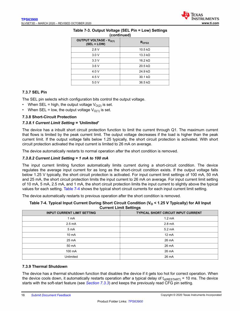
Table 7-3. Output Voltage (SEL Pin = Low) Settings(continued)
OUTPUT VOLTAGE - VO(1)(SEL = LOW) RCFG3
2.8 V 10.5 kΩ
3.0 V 13.3 kΩ
3.3 V 16.2 kΩ
3.6 V 20.5 kΩ
4.0 V 24.9 kΩ
4.5 V 30.1 kΩ
5.0 V 36.5 kΩ
7.3.7 SEL Pin
The SEL pin selects which configuration bits control the output voltage.• When SEL = high, the output voltage VO(2) is set.• When SEL = low, the output voltage VO(1) is set.
7.3.8 Short-Circuit Protection7.3.8.1 Current Limit Setting = 'Unlimited'
The device has a inbuilt short circuit protection function to limit the current through Q1. The maximum currentthat flows is limited by the peak current limit. The output voltage decreases if the load is higher than the peakcurrent limit. If the output voltage falls below 1.25 typically, the short circuit protection is activated. With shortcircuit protection activated the input current is limited to 26 mA on average.
The device automatically restarts to normal operation after the short condition is removed.
7.3.8.2 Current Limit Setting = 1 mA to 100 mA
The input current limiting function automatically limits current during a short-circuit condition. The deviceregulates the average input current for as long as the short-circuit condition exists. If the output voltage fallsbelow 1.25 V typically, the short circuit protection is activated. For input current limit settings of 100 mA, 50 mAand 25 mA, the short circuit protection limits the input current to 26 mA on average. For input current limit settingof 10 mA, 5 mA, 2.5 mA, and 1 mA, the short circuit protection limits the input current to slightly above the typicalvalues for each setting. Table 7-4 shows the typical short circuit currents for each input current limit setting.
The device automatically restarts to previous operation after the short condition is removed.
Table 7-4. Typical Input Current During Short Circuit Condition (VO < 1.25 V Typically) for All InputCurrent Limit Settings
INPUT CURRENT LIMIT SETTING TYPICAL SHORT CIRCUIT INPUT CURRENT1 mA 1.2 mA
2.5 mA 2.8 mA
5 mA 5.2 mA
10 mA 12 mA
25 mA 26 mA
50 mA 26 mA
100 mA 26 mA
Unlimited 26 mA
7.3.9 Thermal Shutdown
The device has a thermal shutdown function that disables the device if it gets too hot for correct operation. Whenthe device cools down, it automatically restarts operation after a typical delay of td(RESTART) = 10 ms. The devicestarts with the soft-start feature (see Section 7.3.3) and keeps the previously read CFG pin setting.
TPS63900SLVSET3D – MARCH 2020 – REVISED OCTOBER 2020 www.ti.com
16 Submit Document Feedback Copyright © 2020 Texas Instruments Incorporated
Product Folder Links: TPS63900
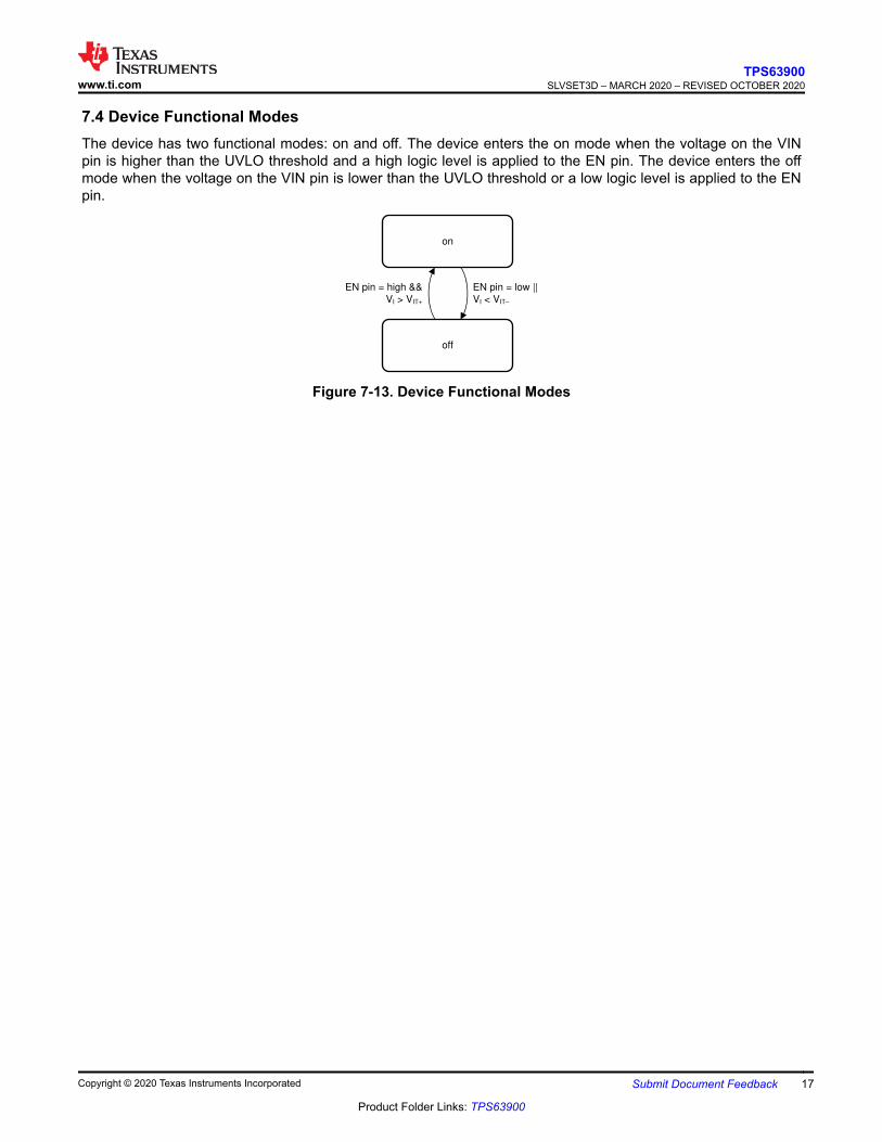
7.4 Device Functional ModesThe device has two functional modes: on and off. The device enters the on mode when the voltage on the VINpin is higher than the UVLO threshold and a high logic level is applied to the EN pin. The device enters the offmode when the voltage on the VIN pin is lower than the UVLO threshold or a low logic level is applied to the ENpin.
off
on
EN pin = high &&
VI > VIT+
EN pin = low ||
VI < VIT±
Figure 7-13. Device Functional Modes
www.ti.comTPS63900
SLVSET3D – MARCH 2020 – REVISED OCTOBER 2020
Copyright © 2020 Texas Instruments Incorporated Submit Document Feedback 17
Product Folder Links: TPS63900
8 Application and ImplementationNote
Information in the following applications sections is not part of the TI component specification, and TIdoes not warrant its accuracy or completeness. TI’s customers are responsible for determiningsuitability of components for their purposes. Customers should validate and test their designimplementation to confirm system functionality.
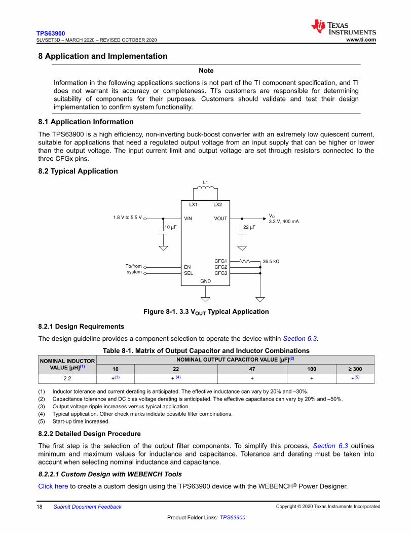
8.1 Application InformationThe TPS63900 is a high efficiency, non-inverting buck-boost converter with an extremely low quiescent current,suitable for applications that need a regulated output voltage from an input supply that can be higher or lowerthan the output voltage. The input current limit and output voltage are set through resistors connected to thethree CFGx pins.
8.2 Typical Application
LX1 LX2
VIN VOUT
GND
1.8 V to 5.5 V VO
3.3 V, 400 mA
L1
CFG3
10 µF 22 µF
To/fromsystem SEL
EN CFG2
CFG1 36.5 N
Figure 8-1. 3.3 VOUT Typical Application
8.2.1 Design Requirements
The design guideline provides a component selection to operate the device within Section 6.3.
Table 8-1. Matrix of Output Capacitor and Inductor CombinationsNOMINAL INDUCTOR
VALUE [µH](1)NOMINAL OUTPUT CAPACITOR VALUE [µF](2)
10 22 47 100 ≥ 3002.2 +(3) + (4) + + +(5)
(1) Inductor tolerance and current derating is anticipated. The effective inductance can vary by 20% and –30%.(2) Capacitance tolerance and DC bias voltage derating is anticipated. The effective capacitance can vary by 20% and –50%.(3) Output voltage ripple increases versus typical application.(4) Typical application. Other check marks indicate possible filter combinations.(5) Start-up time increased.
8.2.2 Detailed Design Procedure
The first step is the selection of the output filter components. To simplify this process, Section 6.3 outlinesminimum and maximum values for inductance and capacitance. Tolerance and derating must be taken intoaccount when selecting nominal inductance and capacitance.
8.2.2.1 Custom Design with WEBENCH Tools
Click here to create a custom design using the TPS63900 device with the WEBENCH® Power Designer.
TPS63900SLVSET3D – MARCH 2020 – REVISED OCTOBER 2020 www.ti.com
18 Submit Document Feedback Copyright © 2020 Texas Instruments Incorporated
Product Folder Links: TPS63900
1. Start by entering your VIN, VOUT and IOUT requirements.2. Optimize your design for key parameters like efficiency, footprint or cost using the optimizer dial and compare
this design with other possible solutions from Texas Instruments.3. WEBENCH Power Designer provides you with a customized schematic along with a list of materials with real
time pricing and component availability.4. In most cases, you will also be able to:
• Run electrical simulations to see important waveforms and circuit performance,• Run thermal simulations to understand the thermal performance of your board,• Export your customized schematic and layout into popular CAD formats,• Print PDF reports for the design, and share your design with colleagues.
5. Get more information about WEBENCH tools at www.ti.com/webench.
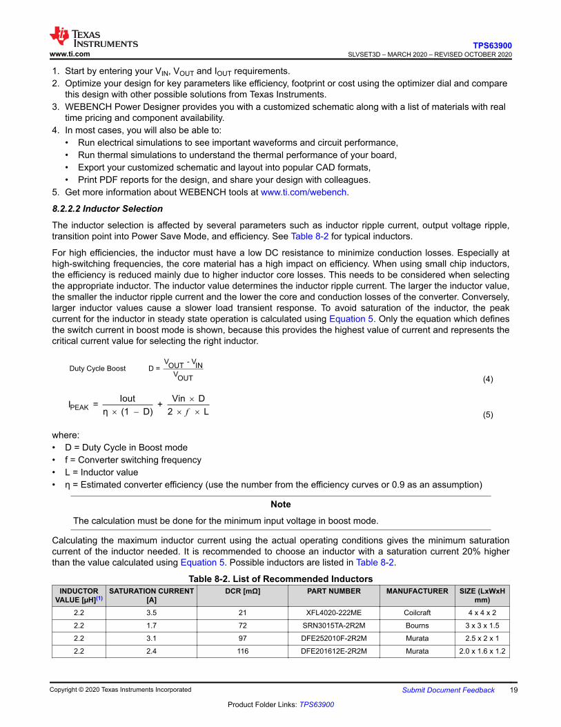
8.2.2.2 Inductor Selection
The inductor selection is affected by several parameters such as inductor ripple current, output voltage ripple,transition point into Power Save Mode, and efficiency. See Table 8-2 for typical inductors.
For high efficiencies, the inductor must have a low DC resistance to minimize conduction losses. Especially athigh-switching frequencies, the core material has a high impact on efficiency. When using small chip inductors,the efficiency is reduced mainly due to higher inductor core losses. This needs to be considered when selectingthe appropriate inductor. The inductor value determines the inductor ripple current. The larger the inductor value,the smaller the inductor ripple current and the lower the core and conduction losses of the converter. Conversely,larger inductor values cause a slower load transient response. To avoid saturation of the inductor, the peakcurrent for the inductor in steady state operation is calculated using Equation 5. Only the equation which definesthe switch current in boost mode is shown, because this provides the highest value of current and represents thecritical current value for selecting the right inductor.
V - VINOUTDuty Cycle Boost D =
VOUT (4)
PEAK
Iout Vin DI = +
η (1 D) 2 L
´
´ - ´ ´f (5)
where:• D = Duty Cycle in Boost mode• f = Converter switching frequency• L = Inductor value• η = Estimated converter efficiency (use the number from the efficiency curves or 0.9 as an assumption)
Note
The calculation must be done for the minimum input voltage in boost mode.
Calculating the maximum inductor current using the actual operating conditions gives the minimum saturationcurrent of the inductor needed. It is recommended to choose an inductor with a saturation current 20% higherthan the value calculated using Equation 5. Possible inductors are listed in Table 8-2.
Table 8-2. List of Recommended InductorsINDUCTOR
VALUE [µH](1)SATURATION CURRENT
[A]DCR [mΩ] PART NUMBER MANUFACTURER SIZE (LxWxH
mm)2.2 3.5 21 XFL4020-222ME Coilcraft 4 x 4 x 2
2.2 1.7 72 SRN3015TA-2R2M Bourns 3 x 3 x 1.5
2.2 3.1 97 DFE252010F-2R2M Murata 2.5 x 2 x 1
2.2 2.4 116 DFE201612E-2R2M Murata 2.0 x 1.6 x 1.2
www.ti.comTPS63900
SLVSET3D – MARCH 2020 – REVISED OCTOBER 2020
Copyright © 2020 Texas Instruments Incorporated Submit Document Feedback 19
Product Folder Links: TPS63900
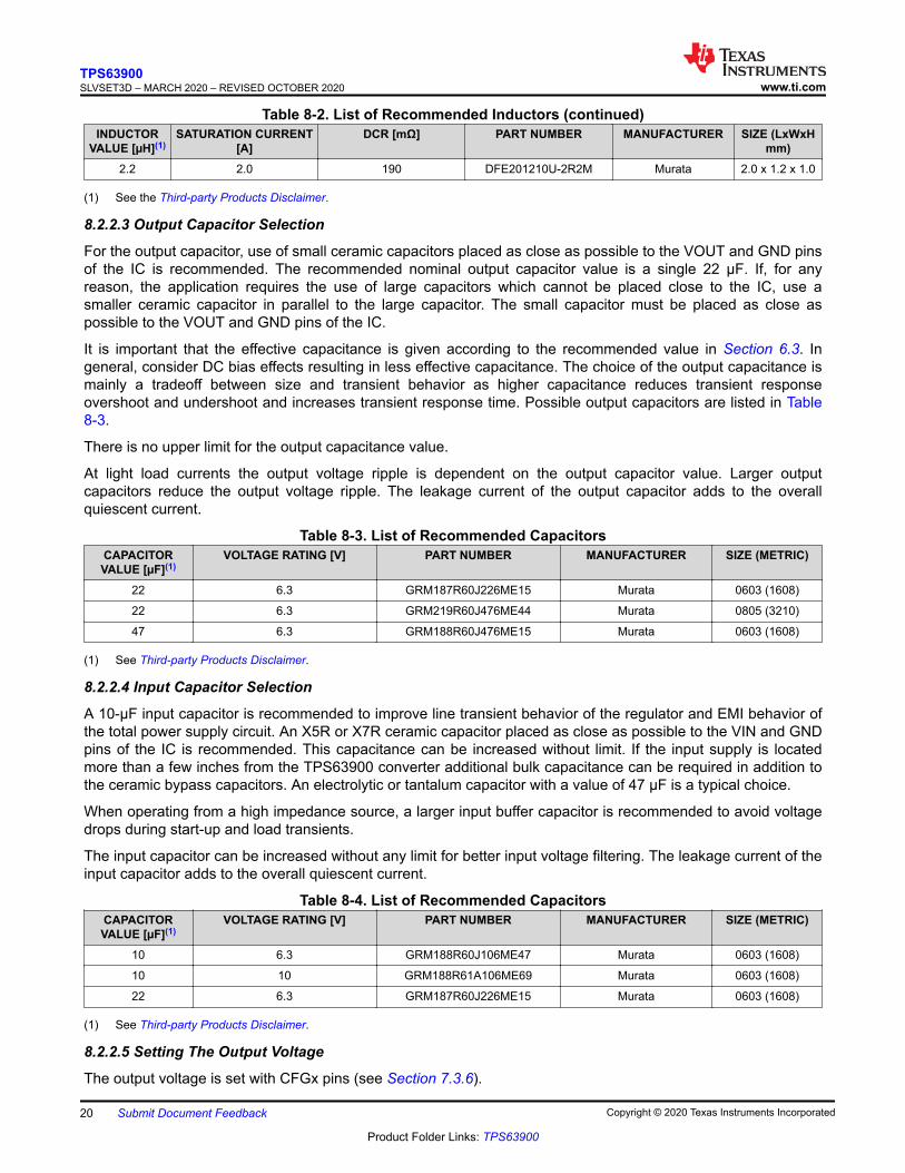
Table 8-2. List of Recommended Inductors (continued)INDUCTOR
VALUE [µH](1)SATURATION CURRENT
[A]DCR [mΩ] PART NUMBER MANUFACTURER SIZE (LxWxH
mm)2.2 2.0 190 DFE201210U-2R2M Murata 2.0 x 1.2 x 1.0
(1) See the Third-party Products Disclaimer.
8.2.2.3 Output Capacitor Selection
For the output capacitor, use of small ceramic capacitors placed as close as possible to the VOUT and GND pinsof the IC is recommended. The recommended nominal output capacitor value is a single 22 µF. If, for anyreason, the application requires the use of large capacitors which cannot be placed close to the IC, use asmaller ceramic capacitor in parallel to the large capacitor. The small capacitor must be placed as close aspossible to the VOUT and GND pins of the IC.
It is important that the effective capacitance is given according to the recommended value in Section 6.3. Ingeneral, consider DC bias effects resulting in less effective capacitance. The choice of the output capacitance ismainly a tradeoff between size and transient behavior as higher capacitance reduces transient responseovershoot and undershoot and increases transient response time. Possible output capacitors are listed in Table8-3.
There is no upper limit for the output capacitance value.
At light load currents the output voltage ripple is dependent on the output capacitor value. Larger outputcapacitors reduce the output voltage ripple. The leakage current of the output capacitor adds to the overallquiescent current.
Table 8-3. List of Recommended CapacitorsCAPACITORVALUE [µF](1)
VOLTAGE RATING [V] PART NUMBER MANUFACTURER SIZE (METRIC)
22 6.3 GRM187R60J226ME15 Murata 0603 (1608)
22 6.3 GRM219R60J476ME44 Murata 0805 (3210)
47 6.3 GRM188R60J476ME15 Murata 0603 (1608)
(1) See Third-party Products Disclaimer.
8.2.2.4 Input Capacitor Selection
A 10-µF input capacitor is recommended to improve line transient behavior of the regulator and EMI behavior ofthe total power supply circuit. An X5R or X7R ceramic capacitor placed as close as possible to the VIN and GNDpins of the IC is recommended. This capacitance can be increased without limit. If the input supply is locatedmore than a few inches from the TPS63900 converter additional bulk capacitance can be required in addition tothe ceramic bypass capacitors. An electrolytic or tantalum capacitor with a value of 47 µF is a typical choice.
When operating from a high impedance source, a larger input buffer capacitor is recommended to avoid voltagedrops during start-up and load transients.
The input capacitor can be increased without any limit for better input voltage filtering. The leakage current of theinput capacitor adds to the overall quiescent current.
Table 8-4. List of Recommended CapacitorsCAPACITORVALUE [µF](1)
VOLTAGE RATING [V] PART NUMBER MANUFACTURER SIZE (METRIC)
10 6.3 GRM188R60J106ME47 Murata 0603 (1608)
10 10 GRM188R61A106ME69 Murata 0603 (1608)
22 6.3 GRM187R60J226ME15 Murata 0603 (1608)
(1) See Third-party Products Disclaimer.
8.2.2.5 Setting The Output Voltage
The output voltage is set with CFGx pins (see Section 7.3.6).
TPS63900SLVSET3D – MARCH 2020 – REVISED OCTOBER 2020 www.ti.com
20 Submit Document Feedback Copyright © 2020 Texas Instruments Incorporated
Product Folder Links: TPS63900
8.2.3 Application Curves
Table 8-5. Components for Application Characteristic Curves for VOUT = 3.3 VREFERENCE(1) DESCRIPTION(2) PART NUMBER MANUFACTURER
U1 400-mA ultra low Iq Buck-Boost Converter (2.5mm x 2.5 mm QFN)
TPS63900DSK Texas Instruments
L1 2.2 µH, 2.5 mm x 2 mm x 1.2 mm, 3.3 A, 82mΩ
DFE252012F-2R2M Murata
C1 10 µF, 0603, Ceramic Capacitor, ±20%, 6.3 V GRM188R60J106ME47 Murata
C2 22 µF, 0603, Ceramic Capacitor, ±20%, 6.3 V GRM187R60J226ME15 Murata
CFG1 36.5 kΩ, 0603 Resistor, 1%, 100 mW Standard Standard
CFG2 0 Ω, 0603 Resistor, 1%, 100 mW Standard Standard
CFG3 0 Ω, 0603 Resistor, 1%, 100 mW Standard Standard
(1) See Third-Party Products Discalimer(2) For other output voltages, refer to Table 8-1 for resistor values.
Table 8-6. Typical Characteristics CurvesPARAMETER CONDITIONS FIGURE
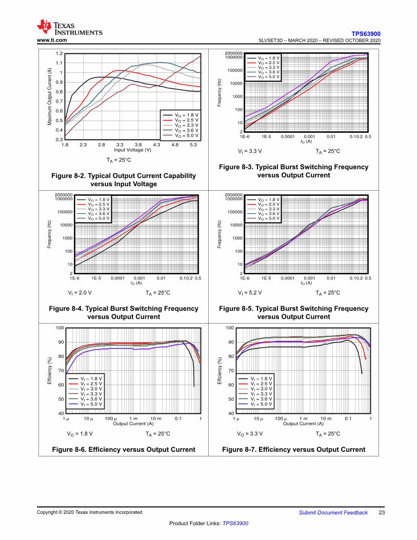
Output Current CapabilityTypical Output Current Capability versus Input Voltage VO = 1.8 V to 5.0 V Figure 8-2
Switching FrequencyTypical Burst Switching Frequency versus Output Current VI = 3.3 V, VO = 1.8 V to 5.0 V Figure 8-3
Typical Burst Switching Frequency versus Output Current VI = 2.0 V, VO = 1.8 V to 5.0 V Figure 8-4
Typical Burst Switching Frequency versus Output Current VI = 5.2 V, VO = 1.8 V to 5.0 V Figure 8-5
EfficiencyEfficiency versus Output Current VI = 1.8 V to 5.5 V, VO = 1.8 V Figure 8-6
Efficiency versus Output Current VI = 1.8 V to 5.5 V, VO = 3.3 V Figure 8-7
Efficiency versus Output Current VI = 1.8 V to 5.5 V, VO = 5.0 V Figure 8-8
Efficiency versus Input Voltage IO = 1 μA to 400 mA, VO = 3.3 V Figure 8-9
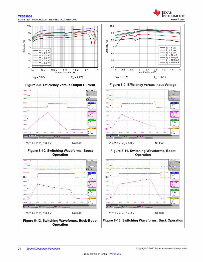
Switching WaveformsSwitching Waveforms, Boost Operation VI = 1.8 V, VO = 3.3 V Figure 8-10
Switching Waveforms, Boost Operation VI = 2.8 V, VO = 3.3 V Figure 8-11
Switching Waveforms, Buck-Boost Operation VI = 3.3 V, VO = 3.3 V Figure 8-12
Switching Waveforms, Buck Operation VI = 4.0 V, VO = 3.3 V Figure 8-13
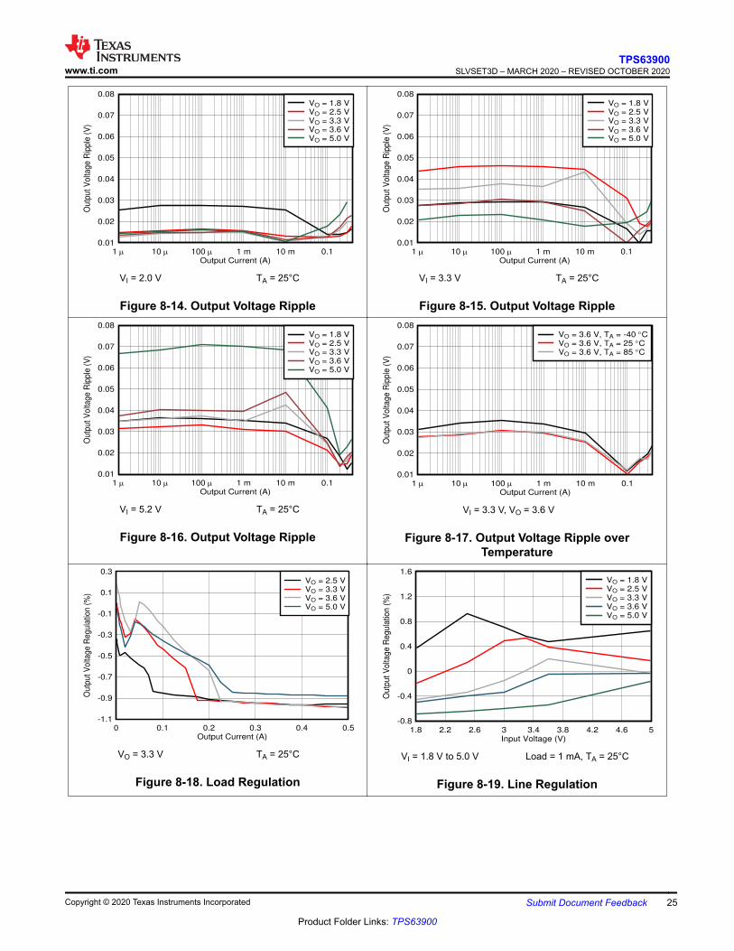
Output Voltage RippleOutput Voltage Ripple VI = 2.0 V, VO = 1.8 V to 5.0 V Figure 8-14
Output Voltage Ripple VI = 3.3 V, VO = 1.8 V to 5.0 V Figure 8-15
Output Voltage Ripple VI = 5.2 V, VO = 1.8 V to 5.0 V Figure 8-16
Output Voltage Ripple over Temperature VI = 3.3 V, VO = 3.6 V Figure 8-17
Regulation AccuracyLoad Regulation VO = 3.3 V Figure 8-18
Line Regulation VI = 1.8 V to 5.0 V, Load = 1 mA Figure 8-19
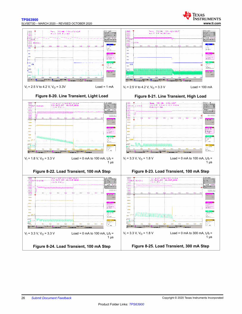
Transient PerformanceLine Transient, Light Load VI = 2.5 V to 4.2 V, VO = 3.3 V, Load = 1 mA Figure 8-20
Line Transient, High Load VI = 2.5 V to 4.2 V, VO = 3.3 V, Load = 100 mA Figure 8-21
Load Transient, 100 mA Step VI = 1.8 V, VO = 3.3 V, Load = 0 mA to 100 mA Figure 8-22
Load Transient, 100 mA Step VI = 3.3 V, VO = 3.3 V, Load = 0 mA to 100 mA Figure 8-23
Load Transient, 100 mA Step VI = 1.8 V, VO = 3.3 V, Load = 0 mA to 100 mA Figure 8-24
Load Transient, 300 mA Step VI = 3.3 V, VO = 1.8 V, Load = 0 mA to 300 mA Figure 8-25
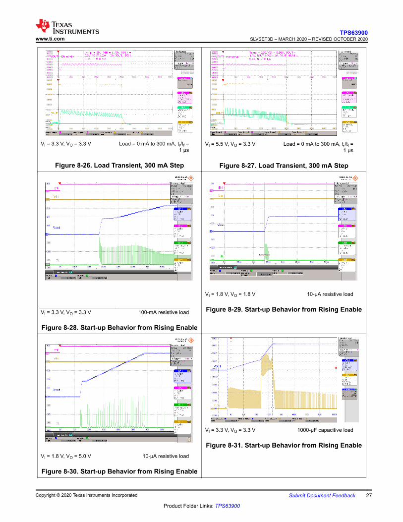
Load Transient, 300 mA Step VI = 3.3 V, VO = 3.3 V, Load = 0 mA to 300 mA Figure 8-26
www.ti.comTPS63900
SLVSET3D – MARCH 2020 – REVISED OCTOBER 2020
Copyright © 2020 Texas Instruments Incorporated Submit Document Feedback 21
Product Folder Links: TPS63900
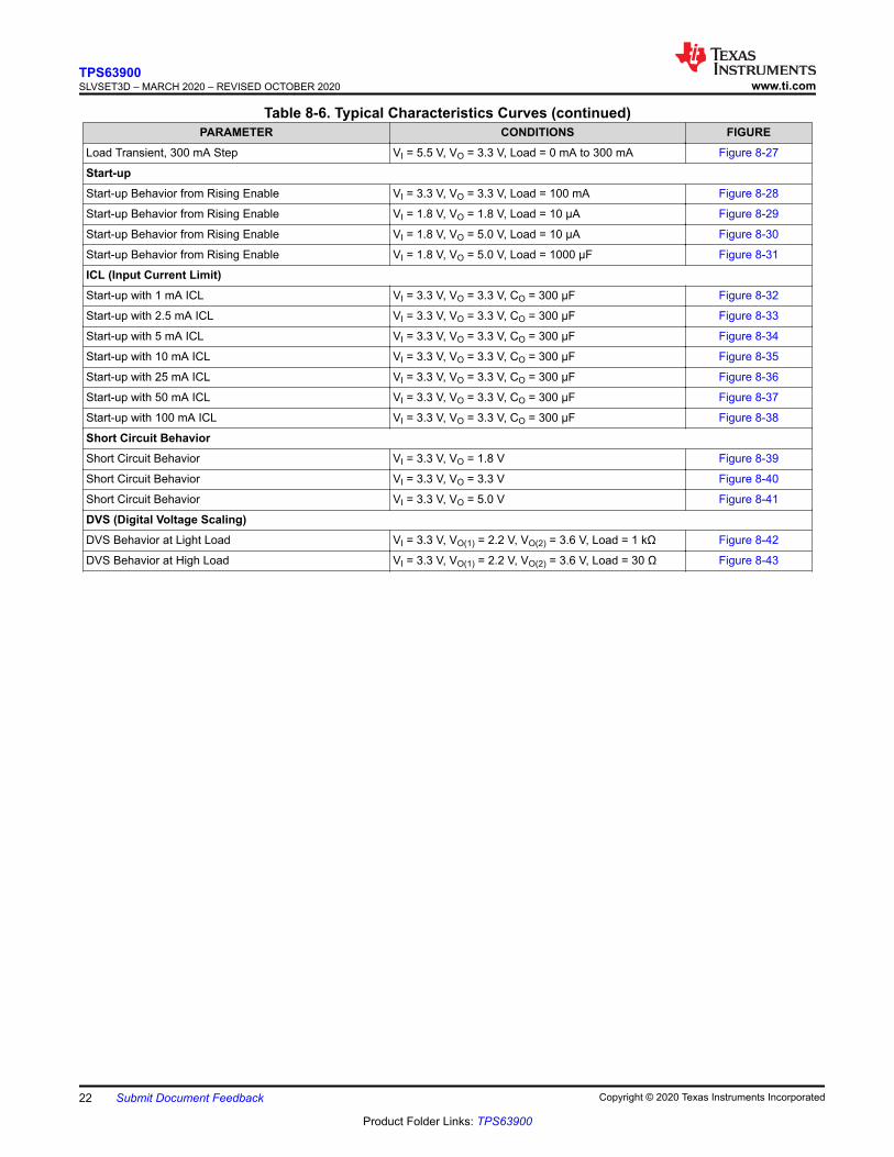
Table 8-6. Typical Characteristics Curves (continued)PARAMETER CONDITIONS FIGURE
Load Transient, 300 mA Step VI = 5.5 V, VO = 3.3 V, Load = 0 mA to 300 mA Figure 8-27
Start-upStart-up Behavior from Rising Enable VI = 3.3 V, VO = 3.3 V, Load = 100 mA Figure 8-28
Start-up Behavior from Rising Enable VI = 1.8 V, VO = 1.8 V, Load = 10 μA Figure 8-29
Start-up Behavior from Rising Enable VI = 1.8 V, VO = 5.0 V, Load = 10 μA Figure 8-30
Start-up Behavior from Rising Enable VI = 1.8 V, VO = 5.0 V, Load = 1000 μF Figure 8-31
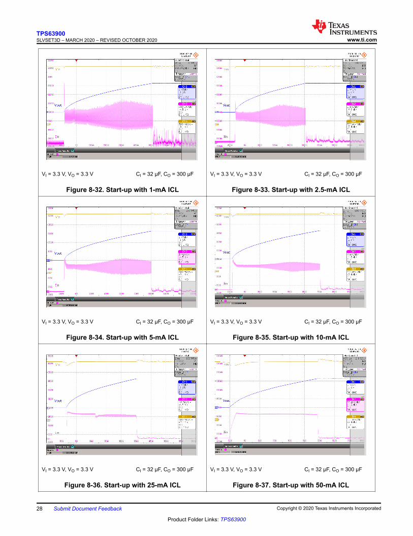
ICL (Input Current Limit)Start-up with 1 mA ICL VI = 3.3 V, VO = 3.3 V, CO = 300 μF Figure 8-32
Start-up with 2.5 mA ICL VI = 3.3 V, VO = 3.3 V, CO = 300 μF Figure 8-33
Start-up with 5 mA ICL VI = 3.3 V, VO = 3.3 V, CO = 300 μF Figure 8-34
Start-up with 10 mA ICL VI = 3.3 V, VO = 3.3 V, CO = 300 μF Figure 8-35
Start-up with 25 mA ICL VI = 3.3 V, VO = 3.3 V, CO = 300 μF Figure 8-36
Start-up with 50 mA ICL VI = 3.3 V, VO = 3.3 V, CO = 300 μF Figure 8-37
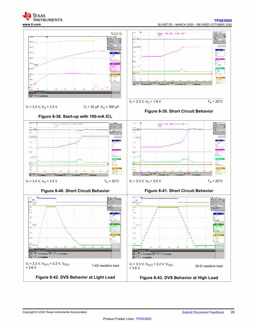
Start-up with 100 mA ICL VI = 3.3 V, VO = 3.3 V, CO = 300 μF Figure 8-38
Short Circuit BehaviorShort Circuit Behavior VI = 3.3 V, VO = 1.8 V Figure 8-39
Short Circuit Behavior VI = 3.3 V, VO = 3.3 V Figure 8-40
Short Circuit Behavior VI = 3.3 V, VO = 5.0 V Figure 8-41
DVS (Digital Voltage Scaling)DVS Behavior at Light Load VI = 3.3 V, VO(1) = 2.2 V, VO(2) = 3.6 V, Load = 1 kΩ Figure 8-42
DVS Behavior at High Load VI = 3.3 V, VO(1) = 2.2 V, VO(2) = 3.6 V, Load = 30 Ω Figure 8-43
TPS63900SLVSET3D – MARCH 2020 – REVISED OCTOBER 2020 www.ti.com
22 Submit Document Feedback Copyright © 2020 Texas Instruments Incorporated
Product Folder Links: TPS63900
Input Voltage (V)
Maxi
mum
Outp
ut
Curr
en
t (A
)
1.8 2.3 2.8 3.3 3.8 4.3 4.8 5.30.3
0.4
0.5
0.6
0.7
0.8
0.9
1
1.1
1.2
VO = 1.8 VVO = 2.5 VVO = 3.3 VVO = 3.6 VVO = 5.0 V
TA = 25°C
Figure 8-2. Typical Output Current Capabilityversus Input Voltage
IO (A)
Fre
qu
en
cy (
Hz)
1E-6 1E-5 0.0001 0.001 0.01 0.10.2 0.52
10
100
1000
10000
100000
10000002000000
VO = 1.8 VVO = 2.5 VVO = 3.3 VVO = 3.6 VVO = 5.0 V
VI = 3.3 V TA = 25°C
Figure 8-3. Typical Burst Switching Frequencyversus Output Current
IO (A)
Fre
qu
en
cy (
Hz)
1E-6 1E-5 0.0001 0.001 0.01 0.10.2 0.52
10
100
1000
10000
100000
10000002000000
VO = 1.8 VVO = 2.5 VVO = 3.3 VVO = 3.6 VVO = 5.0 V
VI = 2.0 V TA = 25°C
Figure 8-4. Typical Burst Switching Frequencyversus Output Current
IO (A)
Fre
qu
en
cy (
Hz)
1E-6 1E-5 0.0001 0.001 0.01 0.10.2 0.52
10
100
1000
10000
100000
10000002000000
VO = 1.8 VVO = 2.5 VVO = 3.3 VVO = 3.6 VVO = 5.0 V
VI = 5.2 V TA = 25°C
Figure 8-5. Typical Burst Switching Frequencyversus Output Current
Output Current (A)
Effic
iency
(%
)
40
50
60
70
80
90
100
1 P 10 P 100 P 1 m 10 m 0.1 1
VI = 1.8 VVI = 2.5 VVI = 3.0 VVI = 3.3 VVI = 3.6 VVI = 5.0 V
VO = 1.8 V TA = 25°C
Figure 8-6. Efficiency versus Output Current
Output Current (A)
Effic
iency
(%
)
40
50
60
70
80
90
100
1 P 10 P 100 P 1 m 10 m 0.1 1
VI = 1.8 VVI = 2.5 VVI = 3.0 VVI = 3.3 VVI = 3.6 VVI = 5.0 V
VO = 3.3 V TA = 25°C
Figure 8-7. Efficiency versus Output Current
www.ti.comTPS63900
SLVSET3D – MARCH 2020 – REVISED OCTOBER 2020
Copyright © 2020 Texas Instruments Incorporated Submit Document Feedback 23
Product Folder Links: TPS63900
Output Current (A)
Effic
iency
(%
)
40
50
60
70
80
90
100
1 P 10 P 100 P 1 m 10 m 0.1 1
VI = 1.8 VVI = 2.5 VVI = 3.0 VVI = 3.3 VVI = 3.6 VVI = 5.0 V
VO = 5.0 V TA = 25°C
Figure 8-8. Efficiency versus Output Current
Input Voltage (V)
Effic
iency
(%
)
1.8 2.2 2.6 3 3.4 3.8 4.2 4.6 540
50
60
70
80
90
100
IO = 1 PAIO = 2 PAIO = 5 PAIO = 10 PAIO = 100 PAIO = 100 mAIO = 400 mA
VO = 3.3 V TA = 25°C
Figure 8-9. Efficiency versus Input Voltage
VI = 1.8 V, VO = 3.3 V No load
Figure 8-10. Switching Waveforms, BoostOperation
VI = 2.8 V, VO = 3.3 V No load
Figure 8-11. Switching Waveforms, BoostOperation
VI = 3.3 V, VO = 3.3 V No load
Figure 8-12. Switching Waveforms, Buck-BoostOperation
VI = 4.0 V, VO = 3.3 V No load
Figure 8-13. Switching Waveforms, Buck Operation
TPS63900SLVSET3D – MARCH 2020 – REVISED OCTOBER 2020 www.ti.com
24 Submit Document Feedback Copyright © 2020 Texas Instruments Incorporated
Product Folder Links: TPS63900
Output Current (A)
Ou
tput
Volta
ge
Rip
ple
(V
)
0.01
0.02
0.03
0.04
0.05
0.06
0.07
0.08
1 P 10 P 100 P 1 m 10 m 0.1
VO = 1.8 VVO = 2.5 VVO = 3.3 VVO = 3.6 VVO = 5.0 V
VI = 2.0 V TA = 25°C
Figure 8-14. Output Voltage Ripple
Output Current (A)
Ou
tput
Volta
ge
Rip
ple
(V
)
0.01
0.02
0.03
0.04
0.05
0.06
0.07
0.08
1 P 10 P 100 P 1 m 10 m 0.1
VO = 1.8 VVO = 2.5 VVO = 3.3 VVO = 3.6 VVO = 5.0 V
VI = 3.3 V TA = 25°C
Figure 8-15. Output Voltage Ripple
Output Current (A)
Ou
tput
Volta
ge
Rip
ple
(V
)
0.01
0.02
0.03
0.04
0.05
0.06
0.07
0.08
1 P 10 P 100 P 1 m 10 m 0.1
VO = 1.8 VVO = 2.5 VVO = 3.3 VVO = 3.6 VVO = 5.0 V
VI = 5.2 V TA = 25°C
Figure 8-16. Output Voltage Ripple
Output Current (A)
Ou
tpu
t V
olta
ge
Rip
ple
(V
)
0.01
0.02
0.03
0.04
0.05
0.06
0.07
0.08
1 P 10 P 100 P 1 m 10 m 0.1
VO = 3.6 V, TA = -40 qCVO = 3.6 V, TA = 25 qCVO = 3.6 V, TA = 85 qC
VI = 3.3 V, VO = 3.6 V
Figure 8-17. Output Voltage Ripple overTemperature
Output Current (A)
Ou
tpu
t V
olta
ge
Re
gu
latio
n (
%)
0 0.1 0.2 0.3 0.4 0.5-1.1
-0.9
-0.7
-0.5
-0.3
-0.1
0.1
0.3VO = 2.5 VVO = 3.3 VVO = 3.6 VVO = 5.0 V
VO = 3.3 V TA = 25°C
Figure 8-18. Load Regulation
Input Voltage (V)
Ou
tpu
t V
olta
ge
Re
gu
latio
n (
%)
1.8 2.2 2.6 3 3.4 3.8 4.2 4.6 5-0.8
-0.4
0
0.4
0.8
1.2
1.6VO = 1.8 VVO = 2.5 VVO = 3.3 VVO = 3.6 VVO = 5.0 V
VI = 1.8 V to 5.0 V Load = 1 mA, TA = 25°C
Figure 8-19. Line Regulation
www.ti.comTPS63900
SLVSET3D – MARCH 2020 – REVISED OCTOBER 2020
Copyright © 2020 Texas Instruments Incorporated Submit Document Feedback 25
Product Folder Links: TPS63900
VI = 2.5 V to 4.2 V, VO = 3.3V Load = 1 mA
Figure 8-20. Line Transient, Light Load
VI = 2.5 V to 4.2 V, VO = 3.3 V Load = 100 mA
Figure 8-21. Line Transient, High Load
VI = 1.8 V, VO = 3.3 V Load = 0 mA to 100 mA, tr/tf =1 μs
Figure 8-22. Load Transient, 100 mA Step
VI = 3.3 V, VO = 1.8 V Load = 0 mA to 100 mA, tr/tf =1 μs
Figure 8-23. Load Transient, 100 mA Step
VI = 3.3 V, VO = 3.3 V Load = 0 mA to 100 mA, tr/tf =1 μs
Figure 8-24. Load Transient, 100 mA Step
VI = 3.3 V, VO = 1.8 V Load = 0 mA to 300 mA, tr/tf =1 μs
Figure 8-25. Load Transient, 300 mA Step
TPS63900SLVSET3D – MARCH 2020 – REVISED OCTOBER 2020 www.ti.com
26 Submit Document Feedback Copyright © 2020 Texas Instruments Incorporated
Product Folder Links: TPS63900
VI = 3.3 V, VO = 3.3 V Load = 0 mA to 300 mA, tr/tf =1 μs
Figure 8-26. Load Transient, 300 mA Step
VI = 5.5 V, VO = 3.3 V Load = 0 mA to 300 mA, tr/tf =1 μs
Figure 8-27. Load Transient, 300 mA Step
VI = 3.3 V, VO = 3.3 V 100-mA resistive load
Figure 8-28. Start-up Behavior from Rising Enable
VI = 1.8 V, VO = 1.8 V 10-μA resistive load
Figure 8-29. Start-up Behavior from Rising Enable
VI = 1.8 V, VO = 5.0 V 10-μA resistive load
Figure 8-30. Start-up Behavior from Rising Enable
VI = 3.3 V, VO = 3.3 V 1000-μF capacitive load
Figure 8-31. Start-up Behavior from Rising Enable
www.ti.comTPS63900
SLVSET3D – MARCH 2020 – REVISED OCTOBER 2020
Copyright © 2020 Texas Instruments Incorporated Submit Document Feedback 27
Product Folder Links: TPS63900
VI = 3.3 V, VO = 3.3 V CI = 32 μF, CO = 300 μF
Figure 8-32. Start-up with 1-mA ICL
VI = 3.3 V, VO = 3.3 V CI = 32 μF, CO = 300 μF
Figure 8-33. Start-up with 2.5-mA ICL
VI = 3.3 V, VO = 3.3 V CI = 32 μF, CO = 300 μF
Figure 8-34. Start-up with 5-mA ICL
VI = 3.3 V, VO = 3.3 V CI = 32 μF, CO = 300 μF
Figure 8-35. Start-up with 10-mA ICL
VI = 3.3 V, VO = 3.3 V CI = 32 μF, CO = 300 μF
Figure 8-36. Start-up with 25-mA ICL
VI = 3.3 V, VO = 3.3 V CI = 32 μF, CO = 300 μF
Figure 8-37. Start-up with 50-mA ICL
TPS63900SLVSET3D – MARCH 2020 – REVISED OCTOBER 2020 www.ti.com
28 Submit Document Feedback Copyright © 2020 Texas Instruments Incorporated
Product Folder Links: TPS63900
VI = 3.3 V, VO = 3.3 V CI = 32 μF, CO = 300 μF
Figure 8-38. Start-up with 100-mA ICL
VI = 3.3 V, VO = 1.8 V TA = 25°C
Figure 8-39. Short Circuit Behavior
VI = 3.3 V, VO = 3.3 V TA = 25°C
Figure 8-40. Short Circuit Behavior
VI = 3.3 V, VO = 5.0 V TA = 25°C
Figure 8-41. Short Circuit Behavior
VI = 3.3 V, VO(1) = 2.2 V, VO(2)= 3.6 V 1-kΩ resistive load
Figure 8-42. DVS Behavior at Light Load
VI = 3.3 V, VO(1) = 2.2 V, VO(2)= 3.6 V 30-Ω resistive load
Figure 8-43. DVS Behavior at High Load
www.ti.comTPS63900
SLVSET3D – MARCH 2020 – REVISED OCTOBER 2020
Copyright © 2020 Texas Instruments Incorporated Submit Document Feedback 29
Product Folder Links: TPS63900
9 Power Supply RecommendationsThe TPS63900 device is designed to operate with input supplies from 1.8 V to 5.5 V. The input supply must bestable and free of noise to achieve the full performance of the device. If the input supply is located more than afew centimeters away from the device, additional bulk capacitance can be required. The input capacitanceshown in the application schematics in this data sheet is sufficient for typical applications.
TPS63900SLVSET3D – MARCH 2020 – REVISED OCTOBER 2020 www.ti.com
30 Submit Document Feedback Copyright © 2020 Texas Instruments Incorporated
Product Folder Links: TPS63900
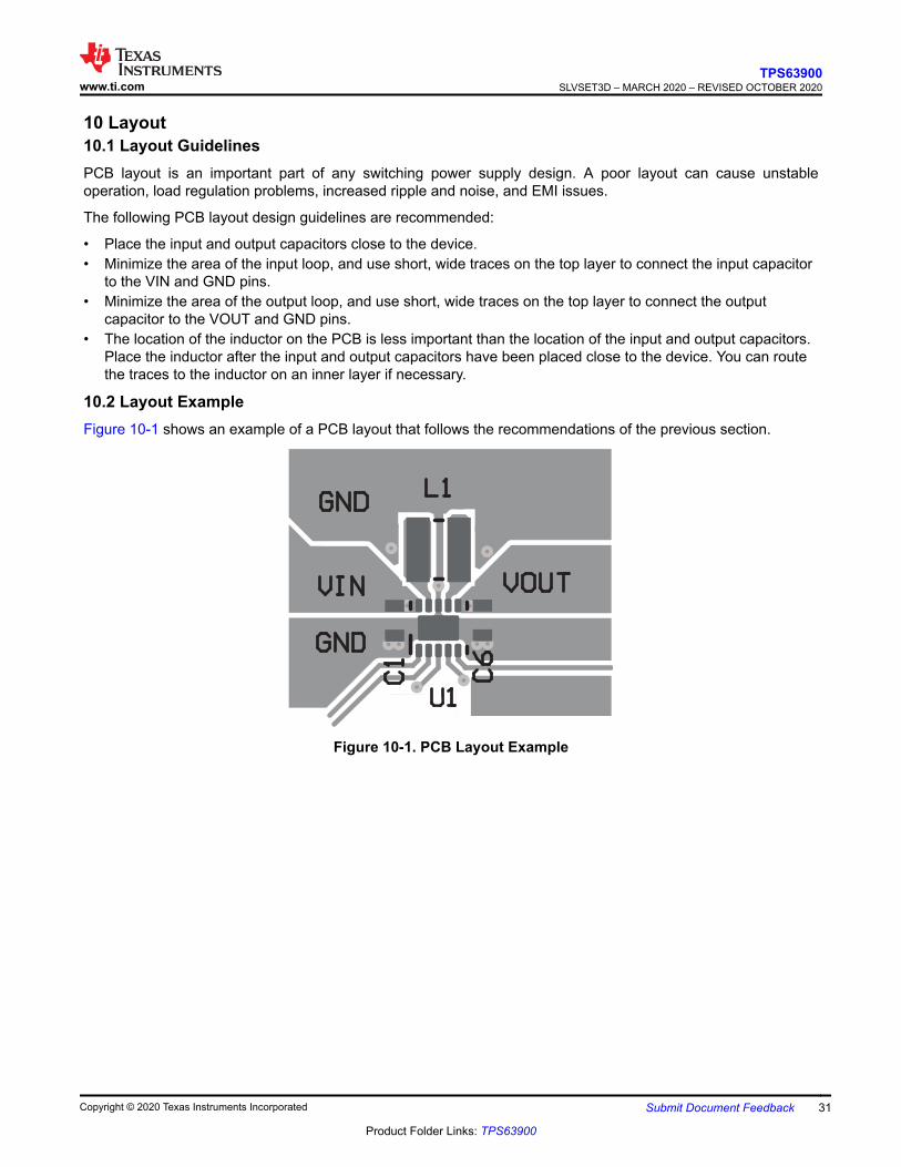
10 Layout10.1 Layout GuidelinesPCB layout is an important part of any switching power supply design. A poor layout can cause unstableoperation, load regulation problems, increased ripple and noise, and EMI issues.
The following PCB layout design guidelines are recommended:
• Place the input and output capacitors close to the device.• Minimize the area of the input loop, and use short, wide traces on the top layer to connect the input capacitor
to the VIN and GND pins.• Minimize the area of the output loop, and use short, wide traces on the top layer to connect the output
capacitor to the VOUT and GND pins.• The location of the inductor on the PCB is less important than the location of the input and output capacitors.
Place the inductor after the input and output capacitors have been placed close to the device. You can routethe traces to the inductor on an inner layer if necessary.
10.2 Layout ExampleFigure 10-1 shows an example of a PCB layout that follows the recommendations of the previous section.
Figure 10-1. PCB Layout Example
www.ti.comTPS63900
SLVSET3D – MARCH 2020 – REVISED OCTOBER 2020
Copyright © 2020 Texas Instruments Incorporated Submit Document Feedback 31
Product Folder Links: TPS63900
11 Device and Documentation Support11.1 Device Support11.1.1 Third-Party Products Disclaimer
TI'S PUBLICATION OF INFORMATION REGARDING THIRD-PARTY PRODUCTS OR SERVICES DOES NOTCONSTITUTE AN ENDORSEMENT REGARDING THE SUITABILITY OF SUCH PRODUCTS OR SERVICESOR A WARRANTY, REPRESENTATION OR ENDORSEMENT OF SUCH PRODUCTS OR SERVICES, EITHERALONE OR IN COMBINATION WITH ANY TI PRODUCT OR SERVICE.
11.2 Documentation Support11.2.1 Related Documentation
For related documentation see the following:
Texas Instruments, TPS63900 EVM User Guide
11.3 Receiving Notification of Documentation UpdatesTo receive notification of documentation updates, navigate to the device product folder on ti.com. Click onSubscribe to updates to register and receive a weekly digest of any product information that has changed. Forchange details, review the revision history included in any revised document.
11.4 Support ResourcesTI E2E™ support forums are an engineer's go-to source for fast, verified answers and design help — straightfrom the experts. Search existing answers or ask your own question to get the quick design help you need.
Linked content is provided "AS IS" by the respective contributors. They do not constitute TI specifications and donot necessarily reflect TI's views; see TI's Terms of Use.
11.5 TrademarksTI E2E™ is a trademark of Texas Instruments.WEBENCH® is a registered trademark of Texas Instruments.All trademarks are the property of their respective owners.11.6 Electrostatic Discharge Caution
This integrated circuit can be damaged by ESD. Texas Instruments recommends that all integrated circuits be handledwith appropriate precautions. Failure to observe proper handling and installation procedures can cause damage.ESD damage can range from subtle performance degradation to complete device failure. Precision integrated circuits maybe more susceptible to damage because very small parametric changes could cause the device not to meet its publishedspecifications.
11.7 GlossaryTI Glossary This glossary lists and explains terms, acronyms, and definitions.
12 Mechanical, Packaging, and Orderable InformationThe following pages include mechanical, packaging, and orderable information. This information is the mostcurrent data available for the designated devices. This data is subject to change without notice and revision ofthis document. For browser-based versions of this data sheet, refer to the left-hand navigation.
TPS63900SLVSET3D – MARCH 2020 – REVISED OCTOBER 2020 www.ti.com
32 Submit Document Feedback Copyright © 2020 Texas Instruments Incorporated
Product Folder Links: TPS63900
PACKAGE OPTION ADDENDUM
www.ti.com 18-Jun-2021
Addendum-Page 1
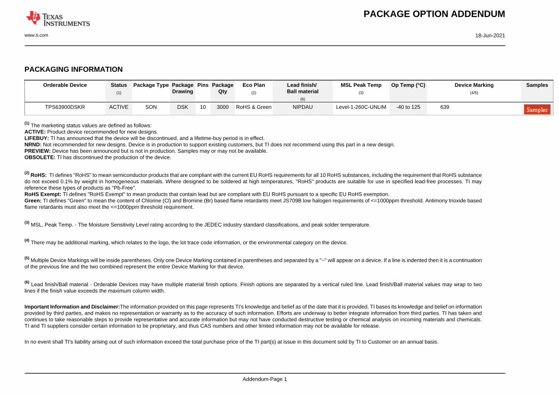
PACKAGING INFORMATION
Orderable Device Status(1)
Package Type PackageDrawing
Pins PackageQty
Eco Plan(2)
Lead finish/Ball material
(6)
MSL Peak Temp(3)
Op Temp (°C) Device Marking(4/5)
Samples
TPS63900DSKR ACTIVE SON DSK 10 3000 RoHS & Green NIPDAU Level-1-260C-UNLIM -40 to 125 639
(1) The marketing status values are defined as follows:ACTIVE: Product device recommended for new designs.LIFEBUY: TI has announced that the device will be discontinued, and a lifetime-buy period is in effect.NRND: Not recommended for new designs. Device is in production to support existing customers, but TI does not recommend using this part in a new design.PREVIEW: Device has been announced but is not in production. Samples may or may not be available.OBSOLETE: TI has discontinued the production of the device.
(2) RoHS: TI defines "RoHS" to mean semiconductor products that are compliant with the current EU RoHS requirements for all 10 RoHS substances, including the requirement that RoHS substancedo not exceed 0.1% by weight in homogeneous materials. Where designed to be soldered at high temperatures, "RoHS" products are suitable for use in specified lead-free processes. TI mayreference these types of products as "Pb-Free".RoHS Exempt: TI defines "RoHS Exempt" to mean products that contain lead but are compliant with EU RoHS pursuant to a specific EU RoHS exemption.Green: TI defines "Green" to mean the content of Chlorine (Cl) and Bromine (Br) based flame retardants meet JS709B low halogen requirements of <=1000ppm threshold. Antimony trioxide basedflame retardants must also meet the <=1000ppm threshold requirement.
(3) MSL, Peak Temp. - The Moisture Sensitivity Level rating according to the JEDEC industry standard classifications, and peak solder temperature.
(4) There may be additional marking, which relates to the logo, the lot trace code information, or the environmental category on the device.
(5) Multiple Device Markings will be inside parentheses. Only one Device Marking contained in parentheses and separated by a "~" will appear on a device. If a line is indented then it is a continuationof the previous line and the two combined represent the entire Device Marking for that device.
(6) Lead finish/Ball material - Orderable Devices may have multiple material finish options. Finish options are separated by a vertical ruled line. Lead finish/Ball material values may wrap to twolines if the finish value exceeds the maximum column width.
Important Information and Disclaimer:The information provided on this page represents TI's knowledge and belief as of the date that it is provided. TI bases its knowledge and belief on informationprovided by third parties, and makes no representation or warranty as to the accuracy of such information. Efforts are underway to better integrate information from third parties. TI has taken andcontinues to take reasonable steps to provide representative and accurate information but may not have conducted destructive testing or chemical analysis on incoming materials and chemicals.TI and TI suppliers consider certain information to be proprietary, and thus CAS numbers and other limited information may not be available for release.
In no event shall TI's liability arising out of such information exceed the total purchase price of the TI part(s) at issue in this document sold by TI to Customer on an annual basis.
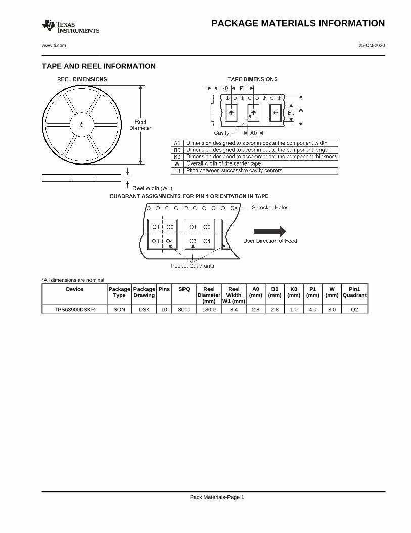
TAPE AND REEL INFORMATION
*All dimensions are nominal
Device PackageType
PackageDrawing
Pins SPQ ReelDiameter
(mm)
ReelWidth
W1 (mm)
A0(mm)
B0(mm)
K0(mm)
P1(mm)
W(mm)
Pin1Quadrant
TPS63900DSKR SON DSK 10 3000 180.0 8.4 2.8 2.8 1.0 4.0 8.0 Q2
PACKAGE MATERIALS INFORMATION
www.ti.com 25-Oct-2020
Pack Materials-Page 1
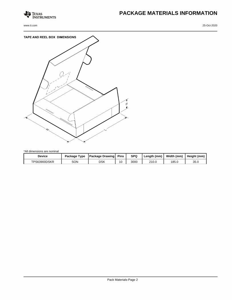
*All dimensions are nominal
Device Package Type Package Drawing Pins SPQ Length (mm) Width (mm) Height (mm)
TPS63900DSKR SON DSK 10 3000 210.0 185.0 35.0
PACKAGE MATERIALS INFORMATION
www.ti.com 25-Oct-2020
Pack Materials-Page 2
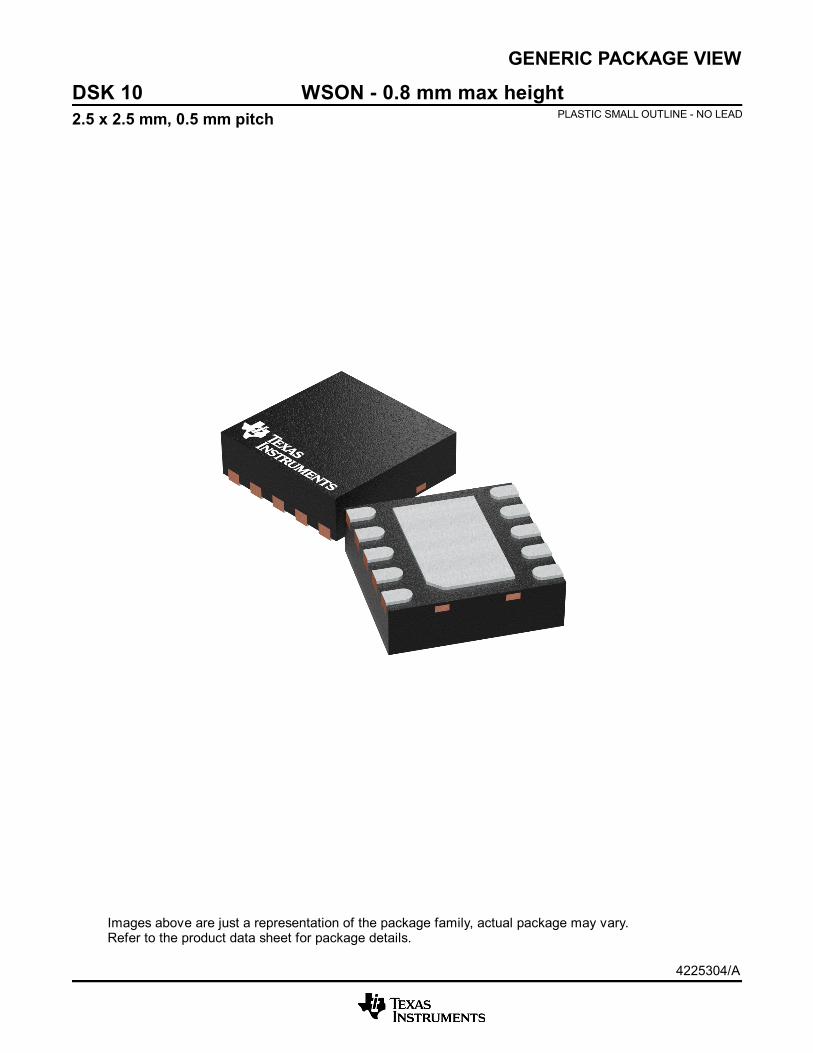
GENERIC PACKAGE VIEW
Images above are just a representation of the package family, actual package may vary.Refer to the product data sheet for package details.
DSK 102.5 x 2.5 mm, 0.5 mm pitch
WSON - 0.8 mm max heightPLASTIC SMALL OUTLINE - NO LEAD
4225304/A
www.ti.com
PACKAGE OUTLINE
C
10X 0.30.2
2 0.1
10X 0.450.35
2X2
1.2 0.1
8X 0.5
0.80.7
0.050.00
B 2.62.4
A
2.62.4
(0.2) TYP
WSON - 0.8 mm max heightDSK0010APLASTIC SMALL OUTLINE - NO LEAD
4218903/B 10/2020
PIN 1 INDEX AREA
SEATING PLANE
0.08 C
1
5
6
10
(OPTIONAL)PIN 1 ID
0.1 C A B0.05 C
THERMAL PADEXPOSED
NOTES: 1. All linear dimensions are in millimeters. Any dimensions in parenthesis are for reference only. Dimensioning and tolerancing per ASME Y14.5M. 2. This drawing is subject to change without notice. 3. The package thermal pad must be soldered to the printed circuit board for thermal and mechanical performance.
11
SCALE 4.000
www.ti.com
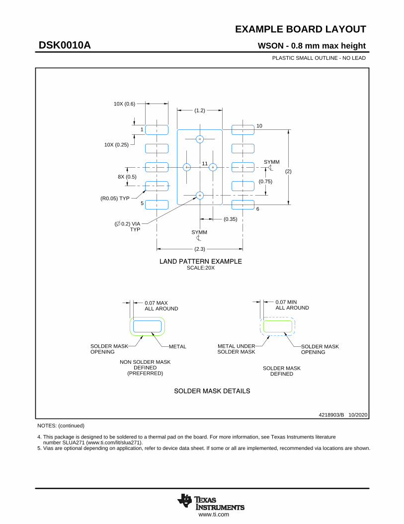
EXAMPLE BOARD LAYOUT
0.07 MINALL AROUND
0.07 MAXALL AROUND
(1.2)
8X (0.5)
(2.3)
10X (0.25)
10X (0.6)
(2)
(R0.05) TYP
( 0.2) VIATYP
(0.75)
(0.35)
WSON - 0.8 mm max heightDSK0010APLASTIC SMALL OUTLINE - NO LEAD
4218903/B 10/2020
SYMM
1
56
10
SYMM
LAND PATTERN EXAMPLESCALE:20X
NOTES: (continued) 4. This package is designed to be soldered to a thermal pad on the board. For more information, see Texas Instruments literature number SLUA271 (www.ti.com/lit/slua271).5. Vias are optional depending on application, refer to device data sheet. If some or all are implemented, recommended via locations are shown.
11
SOLDER MASKOPENINGSOLDER MASK
METAL UNDER
SOLDER MASKDEFINED
METALSOLDER MASKOPENING
SOLDER MASK DETAILS
NON SOLDER MASKDEFINED
(PREFERRED)
www.ti.com
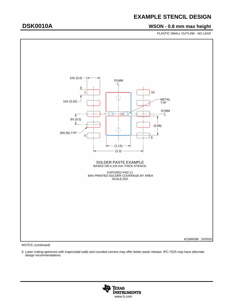
EXAMPLE STENCIL DESIGN
10X (0.25)
10X (0.6)
8X (0.5)
(0.89)
(1.13)
(2.3)
(R0.05) TYP
WSON - 0.8 mm max heightDSK0010APLASTIC SMALL OUTLINE - NO LEAD
4218903/B 10/2020
NOTES: (continued) 6. Laser cutting apertures with trapezoidal walls and rounded corners may offer better paste release. IPC-7525 may have alternate design recommendations.
11
SOLDER PASTE EXAMPLEBASED ON 0.125 mm THICK STENCIL
EXPOSED PAD 11
84% PRINTED SOLDER COVERAGE BY AREASCALE:20X
SYMM
1
5 6
10
SYMM
METALTYP
IMPORTANT NOTICE AND DISCLAIMERTI PROVIDES TECHNICAL AND RELIABILITY DATA (INCLUDING DATASHEETS), DESIGN RESOURCES (INCLUDING REFERENCEDESIGNS), APPLICATION OR OTHER DESIGN ADVICE, WEB TOOLS, SAFETY INFORMATION, AND OTHER RESOURCES “AS IS”AND WITH ALL FAULTS, AND DISCLAIMS ALL WARRANTIES, EXPRESS AND IMPLIED, INCLUDING WITHOUT LIMITATION ANYIMPLIED WARRANTIES OF MERCHANTABILITY, FITNESS FOR A PARTICULAR PURPOSE OR NON-INFRINGEMENT OF THIRDPARTY INTELLECTUAL PROPERTY RIGHTS.These resources are intended for skilled developers designing with TI products. You are solely responsible for (1) selecting the appropriateTI products for your application, (2) designing, validating and testing your application, and (3) ensuring your application meets applicablestandards, and any other safety, security, or other requirements. These resources are subject to change without notice. TI grants youpermission to use these resources only for development of an application that uses the TI products described in the resource. Otherreproduction and display of these resources is prohibited. No license is granted to any other TI intellectual property right or to any third partyintellectual property right. TI disclaims responsibility for, and you will fully indemnify TI and its representatives against, any claims, damages,costs, losses, and liabilities arising out of your use of these resources.TI’s products are provided subject to TI’s Terms of Sale (https:www.ti.com/legal/termsofsale.html) or other applicable terms available eitheron ti.com or provided in conjunction with such TI products. TI’s provision of these resources does not expand or otherwise alter TI’sapplicable warranties or warranty disclaimers for TI products.IMPORTANT NOTICE
Mailing Address: Texas Instruments, Post Office Box 655303, Dallas, Texas 75265Copyright © 2021, Texas Instruments Incorporated