Embed Size (px)
Citation preview
VIN1
8
6
7
3 2
9
5
10
4
10 mH
EN
ILIM
SYNC
GND FC
PG
PGND
FB
L
TPS6200x
†10 mF
VO = 0.8 V
to VI
PG
0.1 mF
10 mF
VI = 2 V
to 5.5 V
† WithVO ≥1.8 V; Co = 10 mF, VO <1.8 V; Co = 47 mF
0
10
20
30
40
50
60
70
80
90
100
0.1 1 10 100 1000
Effic
iency
−%
IO − Load Current − mA
VI = 3.6 V,
VO = 2.5 V
SYNC = Low
SYNC = High
Product
Folder
Sample &Buy
Technical
Documents
Tools &
Software
Support &Community
TPS62000, TPS62001, TPS62002, TPS62003TPS62004, TPS62005, TPS62006, TPS62007, TPS62008
SLVS294F –SEPTEMBER 2000–REVISED AUGUST 2015
TPS6200x High-Efficiency Step-Down Low Power DC-DC Converter1 Features 2 Applications1• High-Efficiency Synchronous Step-Down • Low-Power CPUs and DSPs
Converter with More than 95% Efficiency • Cellular Phones• 2-V to 5.5-V Operating Input Voltage Range • Organizers, PDAs, and Handheld PCs• Adjustable Output Voltage Range From 0.8 V to • MP-3 Portable Audio Players
VIN • Digital Cameras• Fixed Output Voltage Options Available in 0.9 V, • USB-Based DSL Modems and Other Network
1 V, 1.2 V, 1.5 V, 1.8 V, 1.9 V, 2.5 V, and 3.3 V Interface Cards• Synchronizable to External Clock Signal up to
1 MHz 3 Description• Up to 600 mA Output Current The TPS6200x devices are a family of low-noise
synchronous step-down DC/DC converters that are• Pin-Programmable Current Limitideally suited for systems powered from a 1-cell Li-ion• High Efficiency Over a Wide Load Current Range battery or from a 2- to 3-cell NiCd, NiMH, or alkalinein Power Save Mode battery. The TPS6200x operates typically down to an
• 100% Maximum Duty Cycle for Lowest Dropout input voltage of 1.8 V, with a specified minimum inputvoltage of 2 V.• Low-Noise Operation Antiringing Switch and
PFM/PWM Operation Mode The TPS62000 operates over a free-air temperature• Internal Softstart range of –40°C to 85°C.The device is available in the
10-pin (DGS) microsmall outline package (VSSOP).• 50-μA Quiescent Current (TYP)• Available in the 10-Pin Microsmall Outline Device Information(1)
Package (VSSOP)PART NUMBER PACKAGE BODY SIZE (NOM)
• Evaluation Module Available TPS6200x VSSOP (10) 3.00 mm × 3.00 mm
(1) For all available packages, see the orderable addendum atthe end of the datasheet.
Typical Application Schematic Efficiency vs Load Current
1
An IMPORTANT NOTICE at the end of this data sheet addresses availability, warranty, changes, use in safety-critical applications,intellectual property matters and other important disclaimers. PRODUCTION DATA.
TPS62000, TPS62001, TPS62002, TPS62003TPS62004, TPS62005, TPS62006, TPS62007, TPS62008SLVS294F –SEPTEMBER 2000–REVISED AUGUST 2015 www.ti.com
Table of Contents8.4 Device Functional Modes........................................ 101 Features .................................................................. 1
9 Application and Implementation ........................ 122 Applications ........................................................... 19.1 Application Information............................................ 123 Description ............................................................. 19.2 Typical Application .................................................. 124 Revision History..................................................... 29.3 System Examples ................................................... 175 Device Comparison Table ..................................... 3
10 Power Supply Recommendations ..................... 206 Pin Configuration and Functions ......................... 311 Layout................................................................... 207 Specifications......................................................... 4
11.1 Layout Guidelines ................................................. 207.1 Absolute Maximum Ratings ...................................... 411.2 Layout Example .................................................... 207.2 ESD Ratings.............................................................. 4
12 Device and Documentation Support ................. 217.3 Recommended Operating Conditions....................... 412.1 Device Support...................................................... 217.4 Thermal Information .................................................. 412.2 Community Resources.......................................... 217.5 Electrical Characteristics........................................... 512.3 Related Links ........................................................ 217.6 Typical Characteristics .............................................. 712.4 Trademarks ........................................................... 218 Detailed Description .............................................. 812.5 Electrostatic Discharge Caution............................ 218.1 Overview ................................................................... 812.6 Glossary ................................................................ 218.2 Functional Block Diagram ......................................... 9
13 Mechanical, Packaging, and Orderable8.3 Feature Description................................................... 9Information ........................................................... 22
4 Revision HistoryNOTE: Page numbers for previous revisions may differ from page numbers in the current version.
Changes from Revision E (August 2008) to Revision F Page
• Added Pin Configuration and Functions section, ESD Ratings, Feature Description section, Device FunctionalModes, Application and Implementation section, Power Supply Recommendations section, Layout section, Deviceand Documentation Support section, and Mechanical, Packaging, and Orderable Information section .............................. 1
2 Submit Documentation Feedback Copyright © 2000–2015, Texas Instruments Incorporated
Product Folder Links: TPS62000 TPS62001 TPS62002 TPS62003 TPS62004 TPS62005 TPS62006 TPS62007TPS62008
1
2
3
4
5
10
9
8
7
6
VIN
FC
GND
PG
FB
PGND
L
EN
SYNC
ILIM
TPS62000, TPS62001, TPS62002, TPS62003TPS62004, TPS62005, TPS62006, TPS62007, TPS62008
www.ti.com SLVS294F –SEPTEMBER 2000–REVISED AUGUST 2015
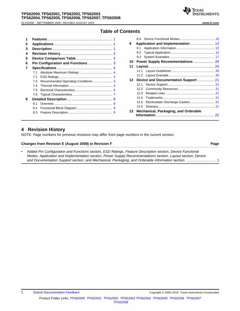
5 Device Comparison Table
PACKAGE (1) MARKINGVOLTAGE OPTIONS
VSSOP DGSAdjustable TPS62000DGS AIH
0.9 V TPS62001DGS AII1 V TPS62002DGS AIJ
1.2 V TPS62003DGS AIK1.5 V TPS62004DGS AIL1.8 V TPS62005DGS AIM1.9 V TPS62008DGS AJI2.5 V TPS62006DGS AIN3.3 V TPS62007DGS AIO
(1) For shipment quantities and additional package information see Mechanical, Packaging, and Orderable Information
6 Pin Configuration and Functions
DGS Package10-Pin VSSOP
Top View
Pin FunctionsPIN
I/O DESCRIPTIONNAME NO.
Enable. A logic high enables the converter, logic low forces the device into shutdown mode reducing theEN 8 I supply current to less than 1 μA.Feedback pin for the fixed output voltage option. For the adjustable version an external resistive divider isFB 5 I connected to FB. The internal voltage divider is disabled for the adjustable version.Supply bypass pin. A 0.1-μF coupling capacitor should be connected as close as possible to this pin forFC 2 — good high frequency input voltage supply filtering.
GND 3 — GroundSwitch current limit. Connect ILIM to GND to set the switch current limit to typically 600 mA, or connect thisILIM 6 I pin to VIN to set the current limit to typically 1200 mA.
L 9 I/O Connect the inductor to this pin. L is the switch pin connected to the drain of the internal power MOSFETS.Power good comparator output. This is an open-drain output. A pull-up resistor should be connected
PG 4 O between PG and VOUT. The output goes active high when the output voltage is greater than 92% of thenominal value.
PGND 10 — Power ground. Connect all power grounds to PGND.Input for synchronization to external clock signal. Synchronizes the converter switching frequency to anexternal clock signal with CMOS level:
SYNC 7 I SYNC = High: Low-noise mode enabled, fixed frequency PWM operation is forcedSYNC = Low (GND): Power save mode enabled, PFM/PWM mode enabled
VIN 1 I Supply voltage input
Copyright © 2000–2015, Texas Instruments Incorporated Submit Documentation Feedback 3
Product Folder Links: TPS62000 TPS62001 TPS62002 TPS62003 TPS62004 TPS62005 TPS62006 TPS62007TPS62008
TPS62000, TPS62001, TPS62002, TPS62003TPS62004, TPS62005, TPS62006, TPS62007, TPS62008SLVS294F –SEPTEMBER 2000–REVISED AUGUST 2015 www.ti.com
7 Specifications
7.1 Absolute Maximum RatingsOver operating free-air temperature range (unless otherwise noted) (1)
MIN MAX UNITSupply voltages on pin VIN and FC (2) –0.3 6 VVoltages on pins EN, ILIM, SYNC, PG, FB, L (2) –0.3 VIN + 0.3 VPeak switch current 1.6 A
TJ Operating junction temperature –40 150 °CLead temperature (soldering, 10 sec) 260 °C
Tstg Storage temperature –65 150 °C
(1) Stresses beyond those listed under Absolute Maximum Ratings may cause permanent damage to the device. These are stress ratingsonly, and functional operation of the device at these or any other conditions beyond those indicated under Recommended OperatingConditions is not implied. Exposure to absolute-maximum-rated conditions for extended periods may affect device reliability.
(2) All voltage values are with respect to network ground terminal.
7.2 ESD RatingsVALUE UNIT
Human body model (HBM), per ANSI/ESDA/JEDEC JS-001 (1) ±2000V(ESD) Electrostatic discharge VCharged device model (CDM), per JEDEC specification JESD22- ±1000
C101 (2)
(1) JEDEC document JEP155 states that 500-V HBM allows safe manufacturing with a standard ESD control process.(2) JEDEC document JEP157 states that 250-V CDM allows safe manufacturing with a standard ESD control process.
7.3 Recommended Operating ConditionsOver operating free-air temperature range (unless otherwise noted)
MIN NOM MAX UNITVIN Supply voltage 2 5.5 VVOUT Output voltage range for adjustable output voltage version 0.8 VIN VIOUT Output current for 3-cell operation (VIN ≥ 2.5 V; L = 10 μH, f = 750 kHz) 600 mAIOUT Output current for 2-cell operation (VIN ≥ 2 V; L = 10 μH, f = 750 kHz) 200 mAL Inductor (1) (see Note 2) 10 μHCIN Input capacitor (1) 10 μFCOUT Output capacitor (1) (VOUT ≥ 1.8 V) 10 μFCOUT Output capacitor (1) VOUT < 1.8 V) 47 μFTA Operating ambient temperature –40 85 °CTJ Operating junction temperature –40 125 °C
(1) Refer to Application Information section for further information.
7.4 Thermal InformationTPS6200x
THERMAL METRIC (1) DGS [VSSOP] UNIT10 PINS
RθJA Junction-to-ambient thermal resistance 160 °C/WRθJC(top) Junction-to-case (top) thermal resistance 51 °C/WRθJB Junction-to-board thermal resistance 73 °C/WψJT Junction-to-top characterization parameter 5.0 °C/WψJB Junction-to-board characterization parameter 72 °C/WRθJC(bot) Junction-to-case (bottom) thermal resistance N/A °C/W
(1) For more information about traditional and new thermal metrics, see the Semiconductor and IC Package Thermal Metrics applicationreport, SPRA953.
4 Submit Documentation Feedback Copyright © 2000–2015, Texas Instruments Incorporated
Product Folder Links: TPS62000 TPS62001 TPS62002 TPS62003 TPS62004 TPS62005 TPS62006 TPS62007TPS62008
TPS62000, TPS62001, TPS62002, TPS62003TPS62004, TPS62005, TPS62006, TPS62007, TPS62008
www.ti.com SLVS294F –SEPTEMBER 2000–REVISED AUGUST 2015
7.5 Electrical CharacteristicsOver recommended operating free-air temperature range, VIN = 3.6 V, VOUT = 2.5 V, IOUT = 300 mA, EN = VIN, ILIM = VIN, TA =–40°C to 85°C (unless otherwise noted)
PARAMETER TEST CONDITIONS MIN TYP MAX UNITSUPPLY CURRENT
IOUT = 0 mA to 600 mA 2.5 5.5VIN Input voltage range V
IOUT = 0 mA to 200 mA 2 5.5I(Q) Operating quiescent current IOUT = 0 mA, SYNC = GND (PFM-mode 50 75 μA
enabled)I(SD) Shutdown current EN = GND 0.1 1 μAENABLEVIH EN high-level input voltage 1.3 VVIL EN low-level input voltage 0.4 VIlkg EN input leakage current EN = GND or VIN 0.01 0.1 μAV(UVLO Undervoltage lockout threshold 1.2 1.6 1.95 V)
POWER SWITCH AND CURRENT LIMITVIN = VGS = 3.6 V, I = 200 mA 200 280 410
P-channel MOSFET on-resistance mΩVIN = VGS = 2 V, I = 200 mA 480
P-channel leakage current VDS = 5.5 V 1 μARDS(on) VIN = VGS = 3.6 V, IOUT = 200 mA 200 280 410
N-channel MOSFET on-resistance mΩVIN = VGS = 2 V, IOUT = 200 mA 500
N-channel leakage current VDS = 5.5 V 1 μA2.5 V ≤ VIN ≤ 5.5 V, ILIM = VIN 800 1200 1600
I(LIM) P-channel current limit mA2 V ≤ VIN ≤ 5.5 V, ILIM = GND 390 600 900
VIH ILIM high-level input voltage 1.3 VVIL ILIM low-level input voltage 0.4 VIlkg ILIM input leakage current ILIM = GND or VIN 0.01 0.1 μAPOWER GOOD OUTPUT (see (1))V(PG) Power good threshold Feedback voltage falling 88% 92% 94% V
VOUT VOUT VOUT
Power good hysteresis 2.5% VVOUT
VOL PG output low voltage V(FB) = 0.8 × VOUT nominal, I(sink) = 10 μA 0.3 VIlkg PG output leakage current V(FB) = VOUT nominal 0.01 1 μA
Minimum supply voltage for valid power good 1.2 Vsignal
OSCILLATORfs Oscillator frequency 500 750 1000 kHzf(SYNC) Synchronization range CMOS-logic clock signal on SYNC pin 500 1000 kHzVIH SYNC high level input voltage 1.3 VVIL SYNC low level input voltage 0.4 VIlkg SYNC input leakage current SYNC = GND or VIN 0.01 0.1 μA
Duty cycle of external clock signal 20% 60%VO Adjustable output voltage TPS62000 0.8 5.5 V
rangeVref Reference voltage TPS6200x 0.45 V
(1) Power good is not valid for the first 100 μs after EN goes high. Refer to the application section for more information.
Copyright © 2000–2015, Texas Instruments Incorporated Submit Documentation Feedback 5
Product Folder Links: TPS62000 TPS62001 TPS62002 TPS62003 TPS62004 TPS62005 TPS62006 TPS62007TPS62008
TPS62000, TPS62001, TPS62002, TPS62003TPS62004, TPS62005, TPS62006, TPS62007, TPS62008SLVS294F –SEPTEMBER 2000–REVISED AUGUST 2015 www.ti.com
Electrical Characteristics (continued)Over recommended operating free-air temperature range, VIN = 3.6 V, VOUT = 2.5 V, IOUT = 300 mA, EN = VIN, ILIM = VIN, TA =–40°C to 85°C (unless otherwise noted)
PARAMETER TEST CONDITIONS MIN TYP MAX UNITVIN = 2.5 V to 5.5 V; 0 mA ≤ IOUT ≤ 600 –3% 4%
TPS62000 mAadjustable
10 mA < IOUT ≤ 600 mA –3% 3%VIN = 2.5 V to 5.5 V; 0 mA ≤ IOUT ≤ 600 –3% 4%
TPS62001 0.9 mAV
10 mA < IOUT ≤ 600 mA –3% 3%VIN = 2.5 V to 5.5 V; 0 mA ≤ IOUT ≤ 600 –3% 4%
TPS62002 mA1 V
10 mA < IOUT ≤ 600 mA –3% 3%VIN = 2.5 V to 5.5 V; 0 mA ≤ IOUT ≤ 600 –3% 4%
TPS62003 mA1.2 V
10 mA < IOUT ≤ 600 mA –3% 3%VIN = 2.5 V to 5.5 V; 0 mA ≤ IOUT ≤ 600 –3% 4%
TPS62004 mAVOUT Fixed output voltage V1.5 V10 mA < IOUT ≤ 600 mA –3% 3%VIN = 2.5 V to 5.5 V; 0 mA ≤ IOUT ≤ 600 –3% 4%
TPS62005 mA1.8 V
10 mA < IOUT ≤ 600 mA –3% 3%VIN = 2.5 V to 5.5 V; 0 mA ≤ IOUT ≤ 600 –3% 4%
TPS62008 mA1.9 V
10 mA < IOUT ≤ 600 mA –3% 3%VIN = 2.7 V to 5.5 V; 0 mA ≤ IOUT ≤ 600 –3% 4%
TPS62006 mA2.5 V
10 mA < IOUT ≤ 600 mA –3% 3%VIN = 3.6 V to 5.5 V; 0 mA ≤ IOUT ≤ 600 –3% 4%
TPS62007 mA3.3 V
10 mA < IOUT ≤ 600 mA –3% 3%Line regulation VIN = VOUT + 0.5 V (min. 2 V) to 5.5 V, 0.05 %/V
IOUT = 10 mALoad regulation VIN = 5.5 V; IOUT = 10 mA to 600 mA 0.6%
VIN = 5 V; VOUT = 3.3 V; IOUT = 300 mAη Efficiency 95%
VIN = 3.6 V; VOUT = 2.5 V; IOUT = 200 mAStart-up time IOUT = 0 mA, time from active EN to VOUT 0.4 2 ms
6 Submit Documentation Feedback Copyright © 2000–2015, Texas Instruments Incorporated
Product Folder Links: TPS62000 TPS62001 TPS62002 TPS62003 TPS62004 TPS62005 TPS62006 TPS62007TPS62008
I-
Op
era
tin
g Q
ue
sc
en
t C
urr
en
t -
A(Q
)m
I-
Op
era
tin
g Q
ue
sc
en
t C
urr
en
t -
A(Q
)m
TPS62000, TPS62001, TPS62002, TPS62003TPS62004, TPS62005, TPS62006, TPS62007, TPS62008
www.ti.com SLVS294F –SEPTEMBER 2000–REVISED AUGUST 2015
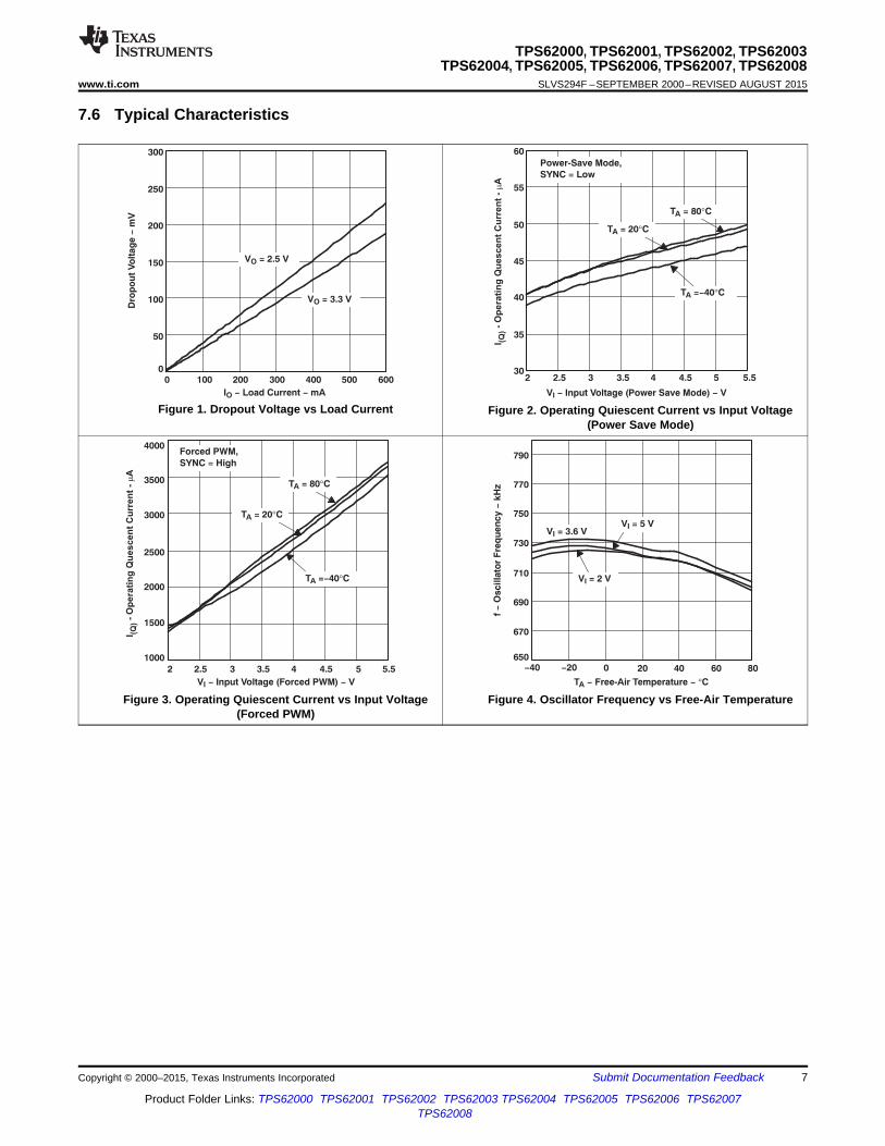
7.6 Typical Characteristics
Figure 1. Dropout Voltage vs Load Current Figure 2. Operating Quiescent Current vs Input Voltage(Power Save Mode)
Figure 3. Operating Quiescent Current vs Input Voltage Figure 4. Oscillator Frequency vs Free-Air Temperature(Forced PWM)
Copyright © 2000–2015, Texas Instruments Incorporated Submit Documentation Feedback 7
Product Folder Links: TPS62000 TPS62001 TPS62002 TPS62003 TPS62004 TPS62005 TPS62006 TPS62007TPS62008
TPS62000, TPS62001, TPS62002, TPS62003TPS62004, TPS62005, TPS62006, TPS62007, TPS62008SLVS294F –SEPTEMBER 2000–REVISED AUGUST 2015 www.ti.com
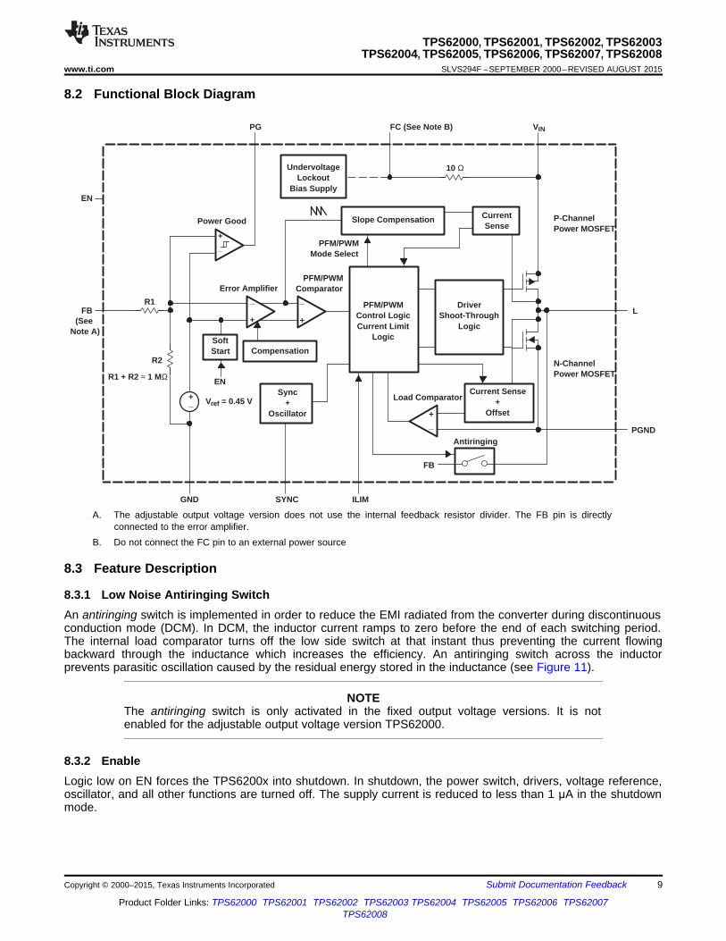
8 Detailed Description
8.1 OverviewThe TPS6200x is a step down converter operating in a current mode PFM/PWM scheme with a typical switchingfrequency of 750 kHz.
At moderate to heavy loads, the converter operates in the pulse width modulation (PWM) and at light loads theconverter enters a power save mode (pulse frequency modulation, PFM) to keep the efficiency high.
In the PWM mode operation, the part operates at a fixed frequency of 750 kHz. At the beginning of each clockcycle, the high side P-channel MOSFET is turned on. The current in the inductor ramps up and is sensed via aninternal circuit. The high side switch is turned off when the sensed current causes the PFM/PWM comparator totrip when the output voltage is in regulation or when the inductor current reaches the current limit (set by ILIM).After a minimum dead time preventing shoot through current, the low side N-channel MOSFET is turned on andthe current ramps down again. As the clock cycle is completed, the low side switch is turned off and the nextclock cycle starts.
In discontinuous conduction mode (DCM), the inductor current ramps to zero before the end of each clock cycle.In order to increase the efficiency the load comparator turns off the low side MOSFET before the inductor currentbecomes negative. This prevents reverse current flowing from the output capacitor through the inductor and lowside MOSFET to ground that would cause additional losses.
As the load current decreases and the peak inductor current does not reach the power save mode threshold oftypically 120 mA for more than 15 clock cycles, the converter enters a pulse frequency modulation (PFM) mode.
In the PFM mode, the converter operates with:• Variable frequency• Constant peak current that reduces switching losses• Quiescent current at a minimum
Thus maintaining the highest efficiency at light load currents. In this mode, the output voltage is monitored withthe error amplifier. As soon as the output voltage falls below the nominal value, the high side switch is turned onand the inductor current ramps up. When the inductor current reaches the peak current of typical: 150 mA +50 mA/V × (VIN – VOUT), the high side switch turns off and the low side switch turns on. As the inductor currentramps down, the low side switch is turned off before the inductor current becomes negative which completes thecycle. When the output voltage falls below the nominal voltage again, the next cycle is started.
The converter enters the PWM mode again as soon as the output voltage can not be maintained with the typicalpeak inductor current in the PFM mode.
The control loop is internally compensated reducing the amount of external components.
The switch current is internally sensed and the maximum current limit can be set to typical 600 mA by connectingILIM to ground; or, to typically 1.2 A by connecting ILIM to VIN.
8 Submit Documentation Feedback Copyright © 2000–2015, Texas Instruments Incorporated
Product Folder Links: TPS62000 TPS62001 TPS62002 TPS62003 TPS62004 TPS62005 TPS62006 TPS62007TPS62008
PFM/PWMControl LogicCurrent Limit
Logic
_
+
CompensationSoftStart
Slope Compensation
PFM/PWMMode Select
PFM/PWMComparatorError Amplifier
_
+
CurrentSense
DriverShoot-Through
Logic
_+
UndervoltageLockout
Bias Supply
10 Ω
_+ Vref = 0.45 V
R2
R1
R1 + R2 ≈ 1 MΩ
Power Good
Sync+
Oscillator_+
Load ComparatorCurrent Sense
+Offset
Antiringing
FB
N-ChannelPower MOSFET
P-ChannelPower MOSFET
L
PGND
EN
FB
PG FC (See Note B) VIN
GND SYNC ILIM
EN
(See Note A)
TPS62000, TPS62001, TPS62002, TPS62003TPS62004, TPS62005, TPS62006, TPS62007, TPS62008
www.ti.com SLVS294F –SEPTEMBER 2000–REVISED AUGUST 2015
8.2 Functional Block Diagram
A. The adjustable output voltage version does not use the internal feedback resistor divider. The FB pin is directlyconnected to the error amplifier.
B. Do not connect the FC pin to an external power source
8.3 Feature Description
8.3.1 Low Noise Antiringing SwitchAn antiringing switch is implemented in order to reduce the EMI radiated from the converter during discontinuousconduction mode (DCM). In DCM, the inductor current ramps to zero before the end of each switching period.The internal load comparator turns off the low side switch at that instant thus preventing the current flowingbackward through the inductance which increases the efficiency. An antiringing switch across the inductorprevents parasitic oscillation caused by the residual energy stored in the inductance (see Figure 11).
NOTEThe antiringing switch is only activated in the fixed output voltage versions. It is notenabled for the adjustable output voltage version TPS62000.
8.3.2 EnableLogic low on EN forces the TPS6200x into shutdown. In shutdown, the power switch, drivers, voltage reference,oscillator, and all other functions are turned off. The supply current is reduced to less than 1 μA in the shutdownmode.
Copyright © 2000–2015, Texas Instruments Incorporated Submit Documentation Feedback 9
Product Folder Links: TPS62000 TPS62001 TPS62002 TPS62003 TPS62004 TPS62005 TPS62006 TPS62007TPS62008
TPS62000, TPS62001, TPS62002, TPS62003TPS62004, TPS62005, TPS62006, TPS62007, TPS62008SLVS294F –SEPTEMBER 2000–REVISED AUGUST 2015 www.ti.com
Feature Description (continued)8.3.3 Undervoltage LockoutAn undervoltage lockout circuit provides the save operation of the device. It prevents the converter from turningon when the voltage on VIN is less than typically 1.6 V.
8.3.4 Power Good ComparatorThe power good (PG) comparator has an open drain output capable of sinking typically 10 μA. The PG is onlyactive when the device is enabled (EN = high). When the device is disabled (EN = low), the PG pin is highimpedance.
The PG output is only valid after a 100 μs delay after the device is enabled and the supply voltage is greaterthan 1.2 V. This is only important in cases where the pullup resistor of the PG pin is connected to an externalvoltage source which might cause an initial spike (false high signal) within the first 100 μs after the input voltageexceeds 1.2 V. This initial spike can be filtered with a small R-C filter to avoid false power good signals duringstart-up.
If the PG pin is connected to the output of the TPS62000 with a pullup resistor, no initial spike (false high signal)occurs and no precautions have to be taken during start-up.
The PG pin becomes active high when the output voltage exceeds typically 94.5% of its nominal value. Leavethe PG pin unconnected when not used.
8.4 Device Functional ModesThe TPS6200x is a synchronous current-mode PWM converter with integrated – and P-channel power MOSFETswitches. Synchronous rectification is used to increase efficiency and to reduce external component count. Toachieve the highest efficiency over a wide load current range, the converter enters a power-saving pulse-frequency modulation (PFM) mode at light load currents. Operating frequency is typically 750 kHz, allowing theuse of small inductor and capacitor values. The device can be synchronized to an external clock signal in therange of 500 kHz to 1 MHz. For low-noise operation, the converter can be operated in the PWM mode and theinternal antiringing switch reduces noise and EMI. In the shutdown mode, the current consumption is reduced toless than 1 μA. The TPS62000 is available in the 10-pin (DGS) microsmall outline package (VSSOP). The deviceoperates over a free-air temperature range of –40°C to 85°C.
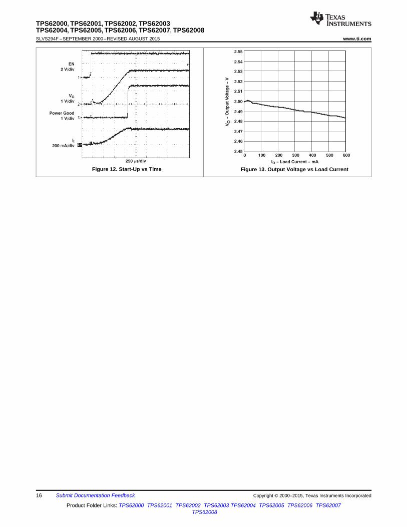
8.4.1 Soft StartAs the enable pin (EN) goes high, the soft-start function generates an internal voltage ramp. This causes thestart-up current to slowly rise preventing output voltage overshoot and high inrush currents. The soft-startduration is typical 1 ms (see Figure 12). When the soft-start function is completed, the error amplifier isconnected directly to the internal voltage reference.
8.4.2 Synchronization, Power Save Mode, and Forced PWM ModeIf no clock signal is applied, the converter operates with a typical switching frequency of 750 kHz. It is possible tosynchronize the converter to an external clock within a frequency range from 500 kHz to 1000 kHz. The deviceautomatically detects the rising edge of the first clock and is synchronized immediately to the external clock. Ifthe clock signal is stopped, the converter automatically switches back to the internal clock and continuesoperation without interruption. The switch over is initiated if no rising edge on the SYNC pin is detected for aduration of four clock cycles. Therefore, the maximum delay time can be 8 μs in case the internal clock has aminimum frequency of 500 kHz.
In case the device is synchronized to an external clock, the power save mode is disabled and the device stays inforced PWM mode.
Connecting the SYNC pin to the GND pin enables the power save mode. The converter operates in the PWMmode at moderate to heavy loads and in the PFM mode during light loads maintaining high efficiency over a wideload current range.
Connecting the SYNC pin to the VIN pin forces the converter to operate permanently in the PWM mode even atlight or no load currents. The advantage is the converter operates with a fixed switching frequency that allowssimple filtering of the switching frequency for noise sensitive applications. In this mode, the efficiency is lowercompared to the power save mode during light loads (see ).
10 Submit Documentation Feedback Copyright © 2000–2015, Texas Instruments Incorporated
Product Folder Links: TPS62000 TPS62001 TPS62002 TPS62003 TPS62004 TPS62005 TPS62006 TPS62007TPS62008
TPS62000, TPS62001, TPS62002, TPS62003TPS62004, TPS62005, TPS62006, TPS62007, TPS62008
www.ti.com SLVS294F –SEPTEMBER 2000–REVISED AUGUST 2015
Device Functional Modes (continued)It is possible to switch from forced PWM mode to the power save mode during operation.
The flexible configuration of the SYNC pin during operation of the device allows efficient power management byadjusting the operation of the TPS6200x to the specific system requirements.
8.4.3 100% Duty Cycle OperationAs the input voltage approaches the output voltage and the duty cycle exceeds typical 95%, the converter turnsthe P-channel high side switch continuously on. In this mode, the output voltage is equal to the input voltageminus the voltage drop across the P-channel MOSFET.
8.4.4 No Load OperationIn case the converter operates in the forced PWM mode and there is no load connected to the output, theconverter will regulate the output voltage by allowing the inductor current to reverse for a short period of time.
Copyright © 2000–2015, Texas Instruments Incorporated Submit Documentation Feedback 11
Product Folder Links: TPS62000 TPS62001 TPS62002 TPS62003 TPS62004 TPS62005 TPS62006 TPS62007TPS62008
472 5
(ff) o
1C = for C F
000 R1m
p³
´ ´
472
(ff) o
1C = for C F
30000 R1m
p<
´ ´
O
R1V = 0.45 V 1 +
R2
æ ö´ ç ÷
è ø
VIN1
8
6
7
3 2
9
5
10
4
L1 = 10 mH
EN
ILIM
SYNC
GND FC
PG
PGND
FB
L
TPS62000
+
Co = 10 mF
VO = 2.5 V/600 mA
C3 = 0.1 mF
Ci = 10 mF
VI = 2.7 V to 5.5 V
R3 = 320 kΩ
R1 = 820 kΩC(ff) =
6.8 pF
R2 = 180 kΩ
+PG
TPS62000, TPS62001, TPS62002, TPS62003TPS62004, TPS62005, TPS62006, TPS62007, TPS62008SLVS294F –SEPTEMBER 2000–REVISED AUGUST 2015 www.ti.com
9 Application and Implementation
NOTEInformation in the following applications sections is not part of the TI componentspecification, and TI does not warrant its accuracy or completeness. TI’s customers areresponsible for determining suitability of components for their purposes. Customers shouldvalidate and test their design implementation to confirm system functionality.
9.1 Application InformationThe TPS6200x device family are highly efficient synchronous step down DC/DC converters providing adjustableoutput voltages from 0.9 V to VIN and fixed output voltages.
9.2 Typical Application
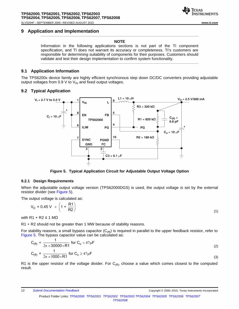
Figure 5. Typical Application Circuit for Adjustable Output Voltage Option
9.2.1 Design RequirementsWhen the adjustable output voltage version (TPS62000DGS) is used, the output voltage is set by the externalresistor divider (see Figure 5).
The output voltage is calculated as:
(1)
with R1 + R2 ≤ 1 MΩ
R1 + R2 should not be greater than 1 MW because of stability reasons.
For stability reasons, a small bypass capacitor (C(ff)) is required in parallel to the upper feedback resistor, refer toFigure 5. The bypass capacitor value can be calculated as:
(2)
(3)
R1 is the upper resistor of the voltage divider. For C(ff), choose a value which comes closest to the computedresult.
12 Submit Documentation Feedback Copyright © 2000–2015, Texas Instruments Incorporated
Product Folder Links: TPS62000 TPS62001 TPS62002 TPS62003 TPS62004 TPS62005 TPS62006 TPS62007TPS62008
2
O
I LL O L(max) O(max)
V1
V II = V I I
L f
-D
D ´ = +´
TPS62000, TPS62001, TPS62002, TPS62003TPS62004, TPS62005, TPS62006, TPS62007, TPS62008
www.ti.com SLVS294F –SEPTEMBER 2000–REVISED AUGUST 2015
Typical Application (continued)9.2.2 Detailed Design Procedure
9.2.2.1 Inductor SelectionA 10 μH minimum output inductor is used with the TPS6200x. Values larger than 22 μH or smaller than 10 μHmay cause stability problems because of the internal compensation of the regulator.
For output voltages greater than 1.8 V, a 22 μH inductance might be used in order to improve the efficiency ofthe converter.
After choosing the inductor value of typically 10 μH, two additional inductor parameters should be considered:first the current rating of the inductor and second the DC resistance.
The DC resistance of the inductance influences directly the efficiency of the converter. Therefore, an inductorwith lowest DC resistance should be selected for highest efficiency.
In order to avoid saturation of the inductor, the inductor should be rated at least for the maximum output currentplus the inductor ripple current which is calculated as:
Where:• ƒ = Switching frequency (750 kHz typical)• L = Inductor value• ΔIL = Peak-to-peak inductor ripple current• IL(max) = Maximum inductor current (4)
The highest inductor current occurs at maximum VIN.
A more conservative approach is to select the inductor current rating just for the maximum switch current of theTPS6200x which is 1.6 A with ILIM = VIN and 900 mA with ILIM = GND. See Table 1 for recommended inductors.
Table 1. Tested InductorsOUTPUT CURRENT INDUCTOR VALUE COMPONENT SUPPLIER COMMENTS
0 mA to 600 mA 10 μH Coilcraft DO3316P-103 High efficiencyCoilcraft DT3316P-103Sumida CDR63B-100
Sumida CDRH5D28-100Coilcraft DO1608C-103 Smallest solution
Sumida CDRH4D28-1000 mA to 300 mA 10 μH Coilcraft DO1608C-103 High efficiency
Murata LQH4C100K04 Smallest solution
9.2.2.2 Output Capacitor SelectionFor best performance, a low ESR output capacitor is needed. At output voltages greater than 1.8 V, ceramicoutput capacitors can be used to show the best performance. Output voltages below 1.8 V require a larger outputcapacitor and ESR value to improve the performance and stability of the converter.
Table 2. Capacitor SelectionOUTPUT VOLTAGE RANGE OUTPUT CAPACITOR OUTPUT CAPACITOR ESR
1.8 V ≤ VIN ≤ 5.5 V Co ≥ 10 μF ESR ≤ 120 mΩ0.8 V ≤ VIN < 1.8 V Co ≥ 47 μF ESR > 50 mΩ
Copyright © 2000–2015, Texas Instruments Incorporated Submit Documentation Feedback 13
Product Folder Links: TPS62000 TPS62001 TPS62002 TPS62003 TPS62004 TPS62005 TPS62006 TPS62007TPS62008
ORMS
II =
2
O ORMS O(max)
I I
V VI = I 1
V V
æ ö´ ´ -ç ÷
è ø
O
IO O
O
V1
V 1V = V ESR
L 8 Cf f
-æ ö
D ´ ´ +ç ÷´ ´ ´è ø
1
2 3O
O
IRMS(C ) O
V1
VI = V
L f
-
´ ´
´ ´
TPS62000, TPS62001, TPS62002, TPS62003TPS62004, TPS62005, TPS62006, TPS62007, TPS62008SLVS294F –SEPTEMBER 2000–REVISED AUGUST 2015 www.ti.com
See Table 3 for recommended capacitors.
If an output capacitor is selected with an ESR value ≤ 120 mΩ, its RMS ripple current rating always meets theapplication requirements. Just for completeness, the RMS ripple current is calculated as:
(5)
The overall output ripple voltage is the sum of the voltage spike caused by the output capacitor ESR plus thevoltage ripple caused by charging and discharging the output capacitor:
(6)
Where the highest output voltage ripple occurs at the highest input voltage VI.
Table 3. Tested CapacitorsCAPACITOR VALUE ESR/mΩ COMPONENT SUPPLIER COMMENTS
10 μF 50 Taiyo Yuden JMK316BJ106KL Ceramic47 μF 100 Sanyo 6TPA47M POSCAP68 μF 100 Spraque 594D686X0010C2T Tantalum
9.2.2.3 Input Capacitor SelectionBecause of the nature of the buck converter having a pulsating input current, a low ESR input capacitor isrequired for best input voltage filtering and minimizing the interference with other circuits caused by high inputvoltage spikes.
The input capacitor should have a minimum value of 10 μF and can be increased without any limit for better inputvoltage filtering.
The input capacitor should be rated for the maximum input ripple current calculated as:
(7)
The worst case RMS ripple current occurs at D = 0.5 and is calculated as:
Ceramic capacitor show a good performance because of their low ESR value, and they are less sensitive againstvoltage transients compared to tantalum capacitors.
Place the input capacitor as close as possible to the input pin of the IC for best performance.
14 Submit Documentation Feedback Copyright © 2000–2015, Texas Instruments Incorporated
Product Folder Links: TPS62000 TPS62001 TPS62002 TPS62003 TPS62004 TPS62005 TPS62006 TPS62007TPS62008
10 s/divm400 s/divm
200 s/divm
40
50
60
70
80
90
100
0.1 1 10 100 1000
VO = 2.5 V
VI = 3.6 V
Eff
icie
ncy
−%
IO − Load Current − mA
VI = 5 V
TPS62000, TPS62001, TPS62002, TPS62003TPS62004, TPS62005, TPS62006, TPS62007, TPS62008
www.ti.com SLVS294F –SEPTEMBER 2000–REVISED AUGUST 2015
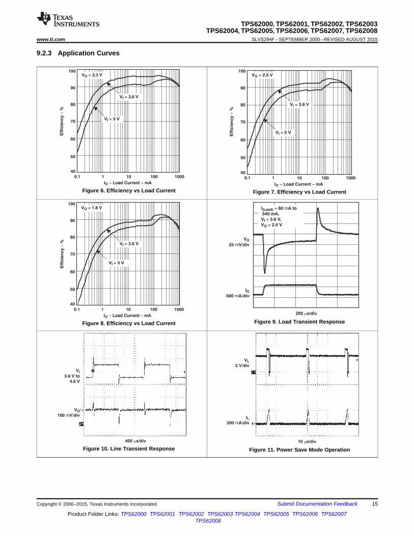
9.2.3 Application Curves
Figure 6. Efficiency vs Load Current Figure 7. Efficiency vs Load Current
Figure 9. Load Transient ResponseFigure 8. Efficiency vs Load Current
Figure 10. Line Transient Response Figure 11. Power Save Mode Operation
Copyright © 2000–2015, Texas Instruments Incorporated Submit Documentation Feedback 15
Product Folder Links: TPS62000 TPS62001 TPS62002 TPS62003 TPS62004 TPS62005 TPS62006 TPS62007TPS62008
2.45
2.46
2.47
2.48
2.49
2.50
2.51
2.52
2.53
2.54
2.55
0 100 200 300 400 500 600
−O
utp
ut
Vo
lta
ge
−V
VO
IO − Load Current − mA
EN
2 V/div
250 ms/div
VO
1 V/div
Power Good
1 V/div
II
200 mA/div
TPS62000, TPS62001, TPS62002, TPS62003TPS62004, TPS62005, TPS62006, TPS62007, TPS62008SLVS294F –SEPTEMBER 2000–REVISED AUGUST 2015 www.ti.com
Figure 12. Start-Up vs Time Figure 13. Output Voltage vs Load Current
16 Submit Documentation Feedback Copyright © 2000–2015, Texas Instruments Incorporated
Product Folder Links: TPS62000 TPS62001 TPS62002 TPS62003 TPS62004 TPS62005 TPS62006 TPS62007TPS62008
VIN1
8
6
7
3 2
9
5
10
4
L1
10 mH
EN
ILIM
SYNC
GND FC
PG
PGND
FB
L
TPS62006DGSC2
10 mF
VO = 2.5 V/600 mA
Power Good
C3
0.1 mF
C1
10 mF
VI = 2.7 V to 4.2 V
470 kΩ
L1: Sumdia CDRH5D28-100
C1,C2: 10 mF Ceramic Taiyo Yuden
JMK316BJ106KL
C3: 0.1 mF Ceramic
VIN1
8
6
7
3 2
9
5
10
4
L1
22 mH
EN
ILIM
SYNC
GND FC
PG
PGND
FB
L
TPS62007DGSC2
10 mF
VO = 3.3 V/600 mA
Power
Good
C3
0.1 mF
C1
10 mF
VI = 5 V
680 kΩ
L1: Sumdia CDRH5D28-220
C1, C2: 10 mF Ceramic Taiyo Yuden
JMK316BJ106KL
C3: 0.1 mF Ceramic
TPS62000, TPS62001, TPS62002, TPS62003TPS62004, TPS62005, TPS62006, TPS62007, TPS62008
www.ti.com SLVS294F –SEPTEMBER 2000–REVISED AUGUST 2015
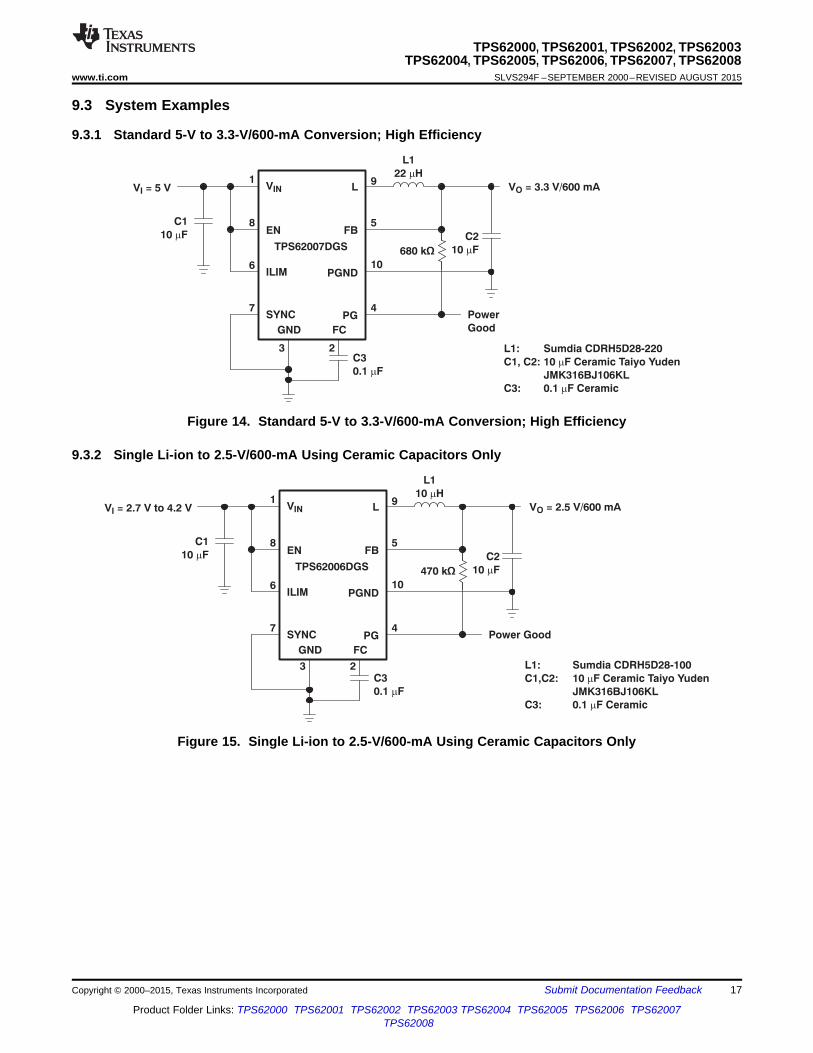
9.3 System Examples
9.3.1 Standard 5-V to 3.3-V/600-mA Conversion; High Efficiency
Figure 14. Standard 5-V to 3.3-V/600-mA Conversion; High Efficiency
9.3.2 Single Li-ion to 2.5-V/600-mA Using Ceramic Capacitors Only
Figure 15. Single Li-ion to 2.5-V/600-mA Using Ceramic Capacitors Only
Copyright © 2000–2015, Texas Instruments Incorporated Submit Documentation Feedback 17
Product Folder Links: TPS62000 TPS62001 TPS62002 TPS62003 TPS62004 TPS62005 TPS62006 TPS62007TPS62008
VIN1
8
6
7
3 2
9
5
10
4
L1
10 mH
EN
ILIM
SYNC
GND FC
PG
PGND
FB
L
TPS62003
+C2
47 mF
VO = 1.2 V/200 mA
C3
0.1 mF
C1
10 mF
VI = 2 V to 3.8 V
L1: Murata LQH4C100K04
C1: 10 mF Ceramic Taiyo Yuden
JMK316BJ106KL
C2: Sanyo 6TPA47M
C3: 0.1 mF Ceramic
VIN1
8
6
7
3 2
9
5
10
4
L1
10 mH
EN
ILIM
SYNC
GND FC
PG
PGND
FB
L
TPS62005DGSC2
10 mF
VO = 1.8 V/300 mA
C3
0.1 mF
C1
10 mF
VI = 2.5 V to 4.2 V
L1: Murata LQH4C100K04
C1,C2: 10 mF Ceramic Taiyo Yuden
JMK316BJ106KL
C3: 0.1 mF Ceramic
TPS62000, TPS62001, TPS62002, TPS62003TPS62004, TPS62005, TPS62006, TPS62007, TPS62008SLVS294F –SEPTEMBER 2000–REVISED AUGUST 2015 www.ti.com
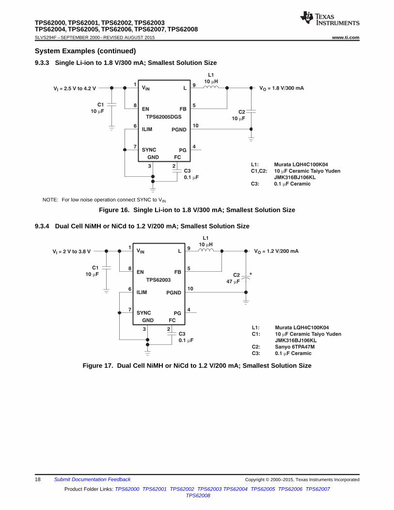
System Examples (continued)9.3.3 Single Li-ion to 1.8 V/300 mA; Smallest Solution Size
NOTE: For low noise operation connect SYNC to VIN
Figure 16. Single Li-ion to 1.8 V/300 mA; Smallest Solution Size
9.3.4 Dual Cell NiMH or NiCd to 1.2 V/200 mA; Smallest Solution Size
Figure 17. Dual Cell NiMH or NiCd to 1.2 V/200 mA; Smallest Solution Size
18 Submit Documentation Feedback Copyright © 2000–2015, Texas Instruments Incorporated
Product Folder Links: TPS62000 TPS62001 TPS62002 TPS62003 TPS62004 TPS62005 TPS62006 TPS62007TPS62008
Sumida CDRH5D28-100
10 F Ceramic Taiyo YudenJMK316BJ106KLSanyo 6TPA47M
0.1 F Ceramic
m
m
0.1 Fm
326 kW 524 kW
47 Fm
470 kW
820 kW
10 Hm
(2)
10 Fm
TPS62000, TPS62001, TPS62002, TPS62003TPS62004, TPS62005, TPS62006, TPS62007, TPS62008
www.ti.com SLVS294F –SEPTEMBER 2000–REVISED AUGUST 2015
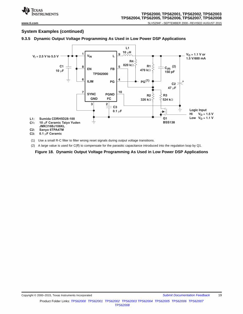
System Examples (continued)9.3.5 Dynamic Output Voltage Programming As Used in Low Power DSP Applications
(1) Use a small R-C filter to filter wrong reset signals during output voltage transitions.(2) A large value is used for C(ff) to compensate for the parasitic capacitance introduced into the regulation loop by Q1.
Figure 18. Dynamic Output Voltage Programming As Used in Low Power DSP Applications
Copyright © 2000–2015, Texas Instruments Incorporated Submit Documentation Feedback 19
Product Folder Links: TPS62000 TPS62001 TPS62002 TPS62003 TPS62004 TPS62005 TPS62006 TPS62007TPS62008
VIN1
8
6
7
3 2
9
5
10
4
L1
EN
ILIM
SYNC
GND FC
PG
PGND
FB
L
TPS62000
+
Co
VO
C3
Ci
VI
R3
R1C(ff)
R2
+PG
TPS62000, TPS62001, TPS62002, TPS62003TPS62004, TPS62005, TPS62006, TPS62007, TPS62008SLVS294F –SEPTEMBER 2000–REVISED AUGUST 2015 www.ti.com
10 Power Supply RecommendationsThe TPS6200x device family has no special requirements for its input power supply. The input power supply'soutput current needs to be rated according to the supply voltage, output voltage and output current of theTPS6200x.
11 Layout
11.1 Layout GuidelinesAs for all switching power supplies, the layout is an important step in the design especially at high peak currentsand switching frequencies. If the layout is not carefully done, the regulator might show stability problems as wellas EMI problems.
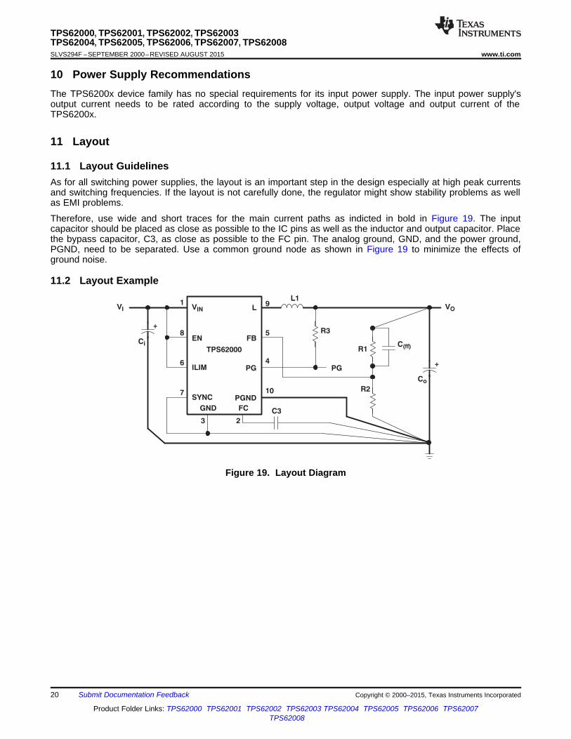
Therefore, use wide and short traces for the main current paths as indicted in bold in Figure 19. The inputcapacitor should be placed as close as possible to the IC pins as well as the inductor and output capacitor. Placethe bypass capacitor, C3, as close as possible to the FC pin. The analog ground, GND, and the power ground,PGND, need to be separated. Use a common ground node as shown in Figure 19 to minimize the effects ofground noise.
11.2 Layout Example
Figure 19. Layout Diagram
20 Submit Documentation Feedback Copyright © 2000–2015, Texas Instruments Incorporated
Product Folder Links: TPS62000 TPS62001 TPS62002 TPS62003 TPS62004 TPS62005 TPS62006 TPS62007TPS62008
TPS62000, TPS62001, TPS62002, TPS62003TPS62004, TPS62005, TPS62006, TPS62007, TPS62008
www.ti.com SLVS294F –SEPTEMBER 2000–REVISED AUGUST 2015
12 Device and Documentation Support
12.1 Device Support
12.1.1 Third-Party Products DisclaimerTI'S PUBLICATION OF INFORMATION REGARDING THIRD-PARTY PRODUCTS OR SERVICES DOES NOTCONSTITUTE AN ENDORSEMENT REGARDING THE SUITABILITY OF SUCH PRODUCTS OR SERVICESOR A WARRANTY, REPRESENTATION OR ENDORSEMENT OF SUCH PRODUCTS OR SERVICES, EITHERALONE OR IN COMBINATION WITH ANY TI PRODUCT OR SERVICE.
12.2 Community ResourcesThe following links connect to TI community resources. Linked contents are provided "AS IS" by the respectivecontributors. They do not constitute TI specifications and do not necessarily reflect TI's views; see TI's Terms ofUse.
TI E2E™ Online Community TI's Engineer-to-Engineer (E2E) Community. Created to foster collaborationamong engineers. At e2e.ti.com, you can ask questions, share knowledge, explore ideas and helpsolve problems with fellow engineers.
Design Support TI's Design Support Quickly find helpful E2E forums along with design support tools andcontact information for technical support.
12.3 Related LinksThe table below lists quick access links. Categories include technical documents, support and communityresources, tools and software, and quick access to sample or buy.
Table 4. Related LinksTECHNICAL TOOLS & SUPPORT &PARTS PRODUCT FOLDER SAMPLE & BUY DOCUMENTS SOFTWARE COMMUNITY
TPS62000 Click here Click here Click here Click here Click hereTPS62001 Click here Click here Click here Click here Click hereTPS62002 Click here Click here Click here Click here Click hereTPS62003 Click here Click here Click here Click here Click hereTPS62004 Click here Click here Click here Click here Click hereTPS62005 Click here Click here Click here Click here Click hereTPS62006 Click here Click here Click here Click here Click hereTPS62007 Click here Click here Click here Click here Click hereTPS62008 Click here Click here Click here Click here Click here
12.4 TrademarksE2E is a trademark of Texas Instruments.All other trademarks are the property of their respective owners.
12.5 Electrostatic Discharge CautionThese devices have limited built-in ESD protection. The leads should be shorted together or the device placed in conductive foamduring storage or handling to prevent electrostatic damage to the MOS gates.
12.6 GlossarySLYZ022 — TI Glossary.
This glossary lists and explains terms, acronyms, and definitions.
Copyright © 2000–2015, Texas Instruments Incorporated Submit Documentation Feedback 21
Product Folder Links: TPS62000 TPS62001 TPS62002 TPS62003 TPS62004 TPS62005 TPS62006 TPS62007TPS62008
TPS62000, TPS62001, TPS62002, TPS62003TPS62004, TPS62005, TPS62006, TPS62007, TPS62008SLVS294F –SEPTEMBER 2000–REVISED AUGUST 2015 www.ti.com
13 Mechanical, Packaging, and Orderable InformationThe following pages include mechanical, packaging, and orderable information. This information is the mostcurrent data available for the designated devices. This data is subject to change without notice and revision ofthis document. For browser-based versions of this data sheet, refer to the left-hand navigation.
22 Submit Documentation Feedback Copyright © 2000–2015, Texas Instruments Incorporated
Product Folder Links: TPS62000 TPS62001 TPS62002 TPS62003 TPS62004 TPS62005 TPS62006 TPS62007TPS62008
PACKAGE OPTION ADDENDUM
www.ti.com 13-Aug-2021
Addendum-Page 1
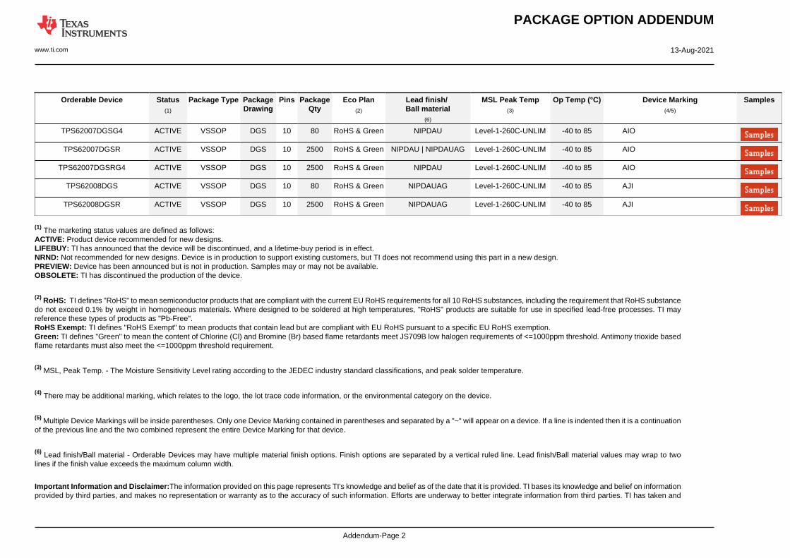
PACKAGING INFORMATION
Orderable Device Status(1)
Package Type PackageDrawing
Pins PackageQty
Eco Plan(2)
Lead finish/Ball material
(6)
MSL Peak Temp(3)
Op Temp (°C) Device Marking(4/5)
Samples
TPS62000DGS ACTIVE VSSOP DGS 10 80 RoHS & Green NIPDAUAG Level-1-260C-UNLIM -40 to 85 AIH
TPS62000DGSG4 ACTIVE VSSOP DGS 10 80 RoHS & Green NIPDAUAG Level-1-260C-UNLIM -40 to 85 AIH
TPS62000DGSR ACTIVE VSSOP DGS 10 2500 RoHS & Green NIPDAU | NIPDAUAG Level-1-260C-UNLIM -40 to 85 AIH
TPS62000DGSRG4 ACTIVE VSSOP DGS 10 2500 RoHS & Green NIPDAU Level-1-260C-UNLIM -40 to 85 AIH
TPS62002DGS ACTIVE VSSOP DGS 10 80 RoHS & Green NIPDAUAG Level-1-260C-UNLIM -40 to 85 AIJ
TPS62002DGSG4 ACTIVE VSSOP DGS 10 80 RoHS & Green NIPDAUAG Level-1-260C-UNLIM -40 to 85 AIJ
TPS62002DGSR ACTIVE VSSOP DGS 10 2500 RoHS & Green NIPDAUAG Level-1-260C-UNLIM -40 to 85 AIJ
TPS62003DGS ACTIVE VSSOP DGS 10 80 RoHS & Green NIPDAUAG Level-1-260C-UNLIM -40 to 85 AIK
TPS62003DGSG4 ACTIVE VSSOP DGS 10 80 RoHS & Green NIPDAUAG Level-1-260C-UNLIM -40 to 85 AIK
TPS62003DGSR ACTIVE VSSOP DGS 10 2500 RoHS & Green NIPDAUAG Level-1-260C-UNLIM -40 to 85 AIK
TPS62003DGSRG4 ACTIVE VSSOP DGS 10 2500 RoHS & Green NIPDAUAG Level-1-260C-UNLIM -40 to 85 AIK
TPS62004DGS ACTIVE VSSOP DGS 10 80 RoHS & Green NIPDAUAG Level-1-260C-UNLIM -40 to 85 AIL
TPS62004DGSG4 ACTIVE VSSOP DGS 10 80 RoHS & Green NIPDAUAG Level-1-260C-UNLIM -40 to 85 AIL
TPS62004DGSR ACTIVE VSSOP DGS 10 2500 RoHS & Green NIPDAUAG Level-1-260C-UNLIM -40 to 85 AIL
TPS62004DGSRG4 ACTIVE VSSOP DGS 10 2500 RoHS & Green NIPDAUAG Level-1-260C-UNLIM -40 to 85 AIL
TPS62005DGS ACTIVE VSSOP DGS 10 80 RoHS & Green NIPDAUAG Level-1-260C-UNLIM -40 to 85 AIM
TPS62005DGSR ACTIVE VSSOP DGS 10 2500 RoHS & Green NIPDAUAG Level-1-260C-UNLIM -40 to 85 AIM
TPS62006DGS ACTIVE VSSOP DGS 10 80 RoHS & Green NIPDAUAG Level-1-260C-UNLIM -40 to 85 AIN
TPS62006DGSR ACTIVE VSSOP DGS 10 2500 RoHS & Green NIPDAUAG Level-1-260C-UNLIM -40 to 85 AIN
TPS62007DGS ACTIVE VSSOP DGS 10 80 RoHS & Green NIPDAU | NIPDAUAG Level-1-260C-UNLIM -40 to 85 AIO
PACKAGE OPTION ADDENDUM
www.ti.com 13-Aug-2021
Addendum-Page 2
Orderable Device Status(1)
Package Type PackageDrawing
Pins PackageQty
Eco Plan(2)
Lead finish/Ball material
(6)
MSL Peak Temp(3)
Op Temp (°C) Device Marking(4/5)
Samples
TPS62007DGSG4 ACTIVE VSSOP DGS 10 80 RoHS & Green NIPDAU Level-1-260C-UNLIM -40 to 85 AIO
TPS62007DGSR ACTIVE VSSOP DGS 10 2500 RoHS & Green NIPDAU | NIPDAUAG Level-1-260C-UNLIM -40 to 85 AIO
TPS62007DGSRG4 ACTIVE VSSOP DGS 10 2500 RoHS & Green NIPDAU Level-1-260C-UNLIM -40 to 85 AIO
TPS62008DGS ACTIVE VSSOP DGS 10 80 RoHS & Green NIPDAUAG Level-1-260C-UNLIM -40 to 85 AJI
TPS62008DGSR ACTIVE VSSOP DGS 10 2500 RoHS & Green NIPDAUAG Level-1-260C-UNLIM -40 to 85 AJI
(1) The marketing status values are defined as follows:ACTIVE: Product device recommended for new designs.LIFEBUY: TI has announced that the device will be discontinued, and a lifetime-buy period is in effect.NRND: Not recommended for new designs. Device is in production to support existing customers, but TI does not recommend using this part in a new design.PREVIEW: Device has been announced but is not in production. Samples may or may not be available.OBSOLETE: TI has discontinued the production of the device.
(2) RoHS: TI defines "RoHS" to mean semiconductor products that are compliant with the current EU RoHS requirements for all 10 RoHS substances, including the requirement that RoHS substancedo not exceed 0.1% by weight in homogeneous materials. Where designed to be soldered at high temperatures, "RoHS" products are suitable for use in specified lead-free processes. TI mayreference these types of products as "Pb-Free".RoHS Exempt: TI defines "RoHS Exempt" to mean products that contain lead but are compliant with EU RoHS pursuant to a specific EU RoHS exemption.Green: TI defines "Green" to mean the content of Chlorine (Cl) and Bromine (Br) based flame retardants meet JS709B low halogen requirements of <=1000ppm threshold. Antimony trioxide basedflame retardants must also meet the <=1000ppm threshold requirement.
(3) MSL, Peak Temp. - The Moisture Sensitivity Level rating according to the JEDEC industry standard classifications, and peak solder temperature.
(4) There may be additional marking, which relates to the logo, the lot trace code information, or the environmental category on the device.
(5) Multiple Device Markings will be inside parentheses. Only one Device Marking contained in parentheses and separated by a "~" will appear on a device. If a line is indented then it is a continuationof the previous line and the two combined represent the entire Device Marking for that device.
(6) Lead finish/Ball material - Orderable Devices may have multiple material finish options. Finish options are separated by a vertical ruled line. Lead finish/Ball material values may wrap to twolines if the finish value exceeds the maximum column width.
Important Information and Disclaimer:The information provided on this page represents TI's knowledge and belief as of the date that it is provided. TI bases its knowledge and belief on informationprovided by third parties, and makes no representation or warranty as to the accuracy of such information. Efforts are underway to better integrate information from third parties. TI has taken and
PACKAGE OPTION ADDENDUM
www.ti.com 13-Aug-2021
Addendum-Page 3
continues to take reasonable steps to provide representative and accurate information but may not have conducted destructive testing or chemical analysis on incoming materials and chemicals.TI and TI suppliers consider certain information to be proprietary, and thus CAS numbers and other limited information may not be available for release.
In no event shall TI's liability arising out of such information exceed the total purchase price of the TI part(s) at issue in this document sold by TI to Customer on an annual basis.
OTHER QUALIFIED VERSIONS OF TPS62000 :
NOTE: Qualified Version Definitions:
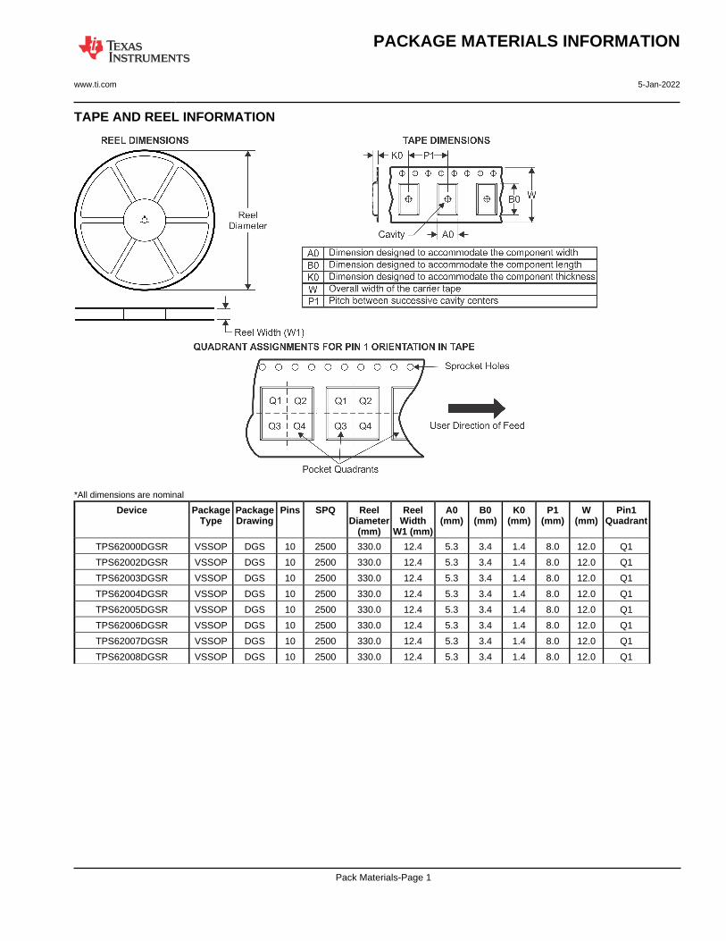
TAPE AND REEL INFORMATION
*All dimensions are nominal
Device PackageType
PackageDrawing
Pins SPQ ReelDiameter
(mm)
ReelWidth
W1 (mm)
A0(mm)
B0(mm)
K0(mm)
P1(mm)
W(mm)
Pin1Quadrant
TPS62000DGSR VSSOP DGS 10 2500 330.0 12.4 5.3 3.4 1.4 8.0 12.0 Q1
TPS62002DGSR VSSOP DGS 10 2500 330.0 12.4 5.3 3.4 1.4 8.0 12.0 Q1
TPS62003DGSR VSSOP DGS 10 2500 330.0 12.4 5.3 3.4 1.4 8.0 12.0 Q1
TPS62004DGSR VSSOP DGS 10 2500 330.0 12.4 5.3 3.4 1.4 8.0 12.0 Q1
TPS62005DGSR VSSOP DGS 10 2500 330.0 12.4 5.3 3.4 1.4 8.0 12.0 Q1
TPS62006DGSR VSSOP DGS 10 2500 330.0 12.4 5.3 3.4 1.4 8.0 12.0 Q1
TPS62007DGSR VSSOP DGS 10 2500 330.0 12.4 5.3 3.4 1.4 8.0 12.0 Q1
TPS62008DGSR VSSOP DGS 10 2500 330.0 12.4 5.3 3.4 1.4 8.0 12.0 Q1
PACKAGE MATERIALS INFORMATION
www.ti.com 5-Jan-2022
Pack Materials-Page 1
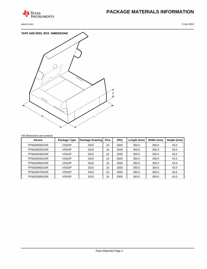
*All dimensions are nominal
Device Package Type Package Drawing Pins SPQ Length (mm) Width (mm) Height (mm)
TPS62000DGSR VSSOP DGS 10 2500 350.0 350.0 43.0
TPS62002DGSR VSSOP DGS 10 2500 350.0 350.0 43.0
TPS62003DGSR VSSOP DGS 10 2500 350.0 350.0 43.0
TPS62004DGSR VSSOP DGS 10 2500 350.0 350.0 43.0
TPS62005DGSR VSSOP DGS 10 2500 350.0 350.0 43.0
TPS62006DGSR VSSOP DGS 10 2500 350.0 350.0 43.0
TPS62007DGSR VSSOP DGS 10 2500 350.0 350.0 43.0
TPS62008DGSR VSSOP DGS 10 2500 350.0 350.0 43.0
PACKAGE MATERIALS INFORMATION
www.ti.com 5-Jan-2022
Pack Materials-Page 2
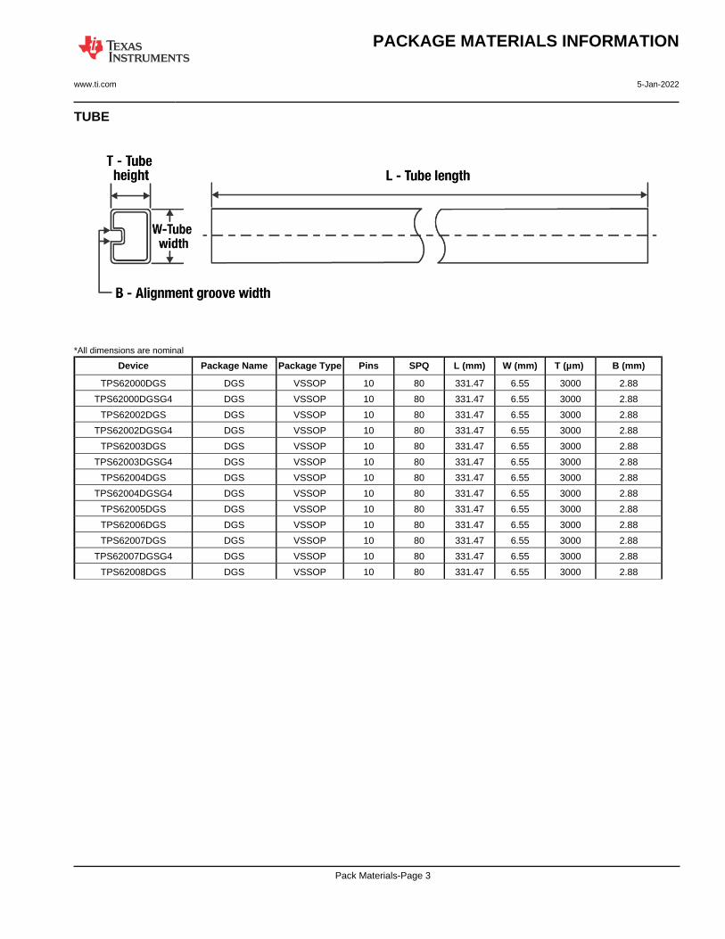
TUBE
*All dimensions are nominal
Device Package Name Package Type Pins SPQ L (mm) W (mm) T (µm) B (mm)
TPS62000DGS DGS VSSOP 10 80 331.47 6.55 3000 2.88
TPS62000DGSG4 DGS VSSOP 10 80 331.47 6.55 3000 2.88
TPS62002DGS DGS VSSOP 10 80 331.47 6.55 3000 2.88
TPS62002DGSG4 DGS VSSOP 10 80 331.47 6.55 3000 2.88
TPS62003DGS DGS VSSOP 10 80 331.47 6.55 3000 2.88
TPS62003DGSG4 DGS VSSOP 10 80 331.47 6.55 3000 2.88
TPS62004DGS DGS VSSOP 10 80 331.47 6.55 3000 2.88
TPS62004DGSG4 DGS VSSOP 10 80 331.47 6.55 3000 2.88
TPS62005DGS DGS VSSOP 10 80 331.47 6.55 3000 2.88
TPS62006DGS DGS VSSOP 10 80 331.47 6.55 3000 2.88
TPS62007DGS DGS VSSOP 10 80 331.47 6.55 3000 2.88
TPS62007DGSG4 DGS VSSOP 10 80 331.47 6.55 3000 2.88
TPS62008DGS DGS VSSOP 10 80 331.47 6.55 3000 2.88
PACKAGE MATERIALS INFORMATION
www.ti.com 5-Jan-2022
Pack Materials-Page 3
www.ti.com
PACKAGE OUTLINE
C
TYP5.054.75
1.1 MAX
8X 0.5
10X 0.270.17
2X2
0.150.05
TYP0.230.13
0 - 8
0.25GAGE PLANE
0.70.4
A
NOTE 3
3.12.9
BNOTE 4
3.12.9
4221984/A 05/2015
VSSOP - 1.1 mm max heightDGS0010ASMALL OUTLINE PACKAGE
NOTES: 1. All linear dimensions are in millimeters. Any dimensions in parenthesis are for reference only. Dimensioning and tolerancing per ASME Y14.5M. 2. This drawing is subject to change without notice. 3. This dimension does not include mold flash, protrusions, or gate burrs. Mold flash, protrusions, or gate burrs shall not exceed 0.15 mm per side. 4. This dimension does not include interlead flash. Interlead flash shall not exceed 0.25 mm per side.5. Reference JEDEC registration MO-187, variation BA.
110
0.1 C A B
65
PIN 1 IDAREA
SEATING PLANE
0.1 C
SEE DETAIL A
DETAIL ATYPICAL
SCALE 3.200
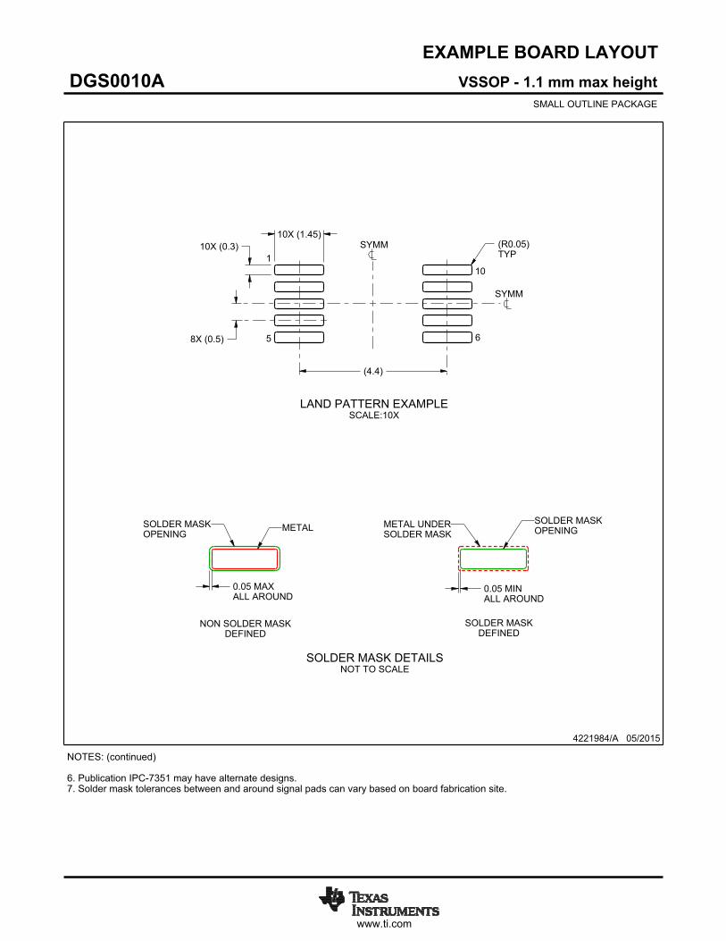
www.ti.com
EXAMPLE BOARD LAYOUT
(4.4)
0.05 MAXALL AROUND
0.05 MINALL AROUND
10X (1.45)10X (0.3)
8X (0.5)
(R )TYP
0.05
4221984/A 05/2015
VSSOP - 1.1 mm max heightDGS0010ASMALL OUTLINE PACKAGE
SYMM
SYMM
LAND PATTERN EXAMPLESCALE:10X
1
5 6
10
NOTES: (continued) 6. Publication IPC-7351 may have alternate designs. 7. Solder mask tolerances between and around signal pads can vary based on board fabrication site.
METALSOLDER MASKOPENING
NON SOLDER MASKDEFINED
SOLDER MASK DETAILSNOT TO SCALE
SOLDER MASKOPENING
METAL UNDERSOLDER MASK
SOLDER MASKDEFINED
www.ti.com
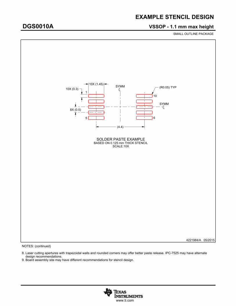
EXAMPLE STENCIL DESIGN
(4.4)
8X (0.5)
10X (0.3)10X (1.45)
(R ) TYP0.05
4221984/A 05/2015
VSSOP - 1.1 mm max heightDGS0010ASMALL OUTLINE PACKAGE
NOTES: (continued) 8. Laser cutting apertures with trapezoidal walls and rounded corners may offer better paste release. IPC-7525 may have alternate design recommendations. 9. Board assembly site may have different recommendations for stencil design.
SYMM
SYMM
1
5 6
10
SOLDER PASTE EXAMPLEBASED ON 0.125 mm THICK STENCIL
SCALE:10X
IMPORTANT NOTICE AND DISCLAIMERTI PROVIDES TECHNICAL AND RELIABILITY DATA (INCLUDING DATA SHEETS), DESIGN RESOURCES (INCLUDING REFERENCE DESIGNS), APPLICATION OR OTHER DESIGN ADVICE, WEB TOOLS, SAFETY INFORMATION, AND OTHER RESOURCES “AS IS” AND WITH ALL FAULTS, AND DISCLAIMS ALL WARRANTIES, EXPRESS AND IMPLIED, INCLUDING WITHOUT LIMITATION ANY IMPLIED WARRANTIES OF MERCHANTABILITY, FITNESS FOR A PARTICULAR PURPOSE OR NON-INFRINGEMENT OF THIRD PARTY INTELLECTUAL PROPERTY RIGHTS.These resources are intended for skilled developers designing with TI products. You are solely responsible for (1) selecting the appropriate TI products for your application, (2) designing, validating and testing your application, and (3) ensuring your application meets applicable standards, and any other safety, security, regulatory or other requirements.These resources are subject to change without notice. TI grants you permission to use these resources only for development of an application that uses the TI products described in the resource. Other reproduction and display of these resources is prohibited. No license is granted to any other TI intellectual property right or to any third party intellectual property right. TI disclaims responsibility for, and you will fully indemnify TI and its representatives against, any claims, damages, costs, losses, and liabilities arising out of your use of these resources.TI’s products are provided subject to TI’s Terms of Sale or other applicable terms available either on ti.com or provided in conjunction with such TI products. TI’s provision of these resources does not expand or otherwise alter TI’s applicable warranties or warranty disclaimers for TI products.TI objects to and rejects any additional or different terms you may have proposed. IMPORTANT NOTICE
Mailing Address: Texas Instruments, Post Office Box 655303, Dallas, Texas 75265Copyright © 2022, Texas Instruments Incorporated