Embed Size (px)
Citation preview

L1
68mH D1
IFB1
ISNS
VIN
VDD
ISET
AGND
TPS61196
GDRV
FSW
C1
10mF
PWM2
VIN = 24V
OVP
R3
EN
R19
R6
C6
C5PGND
COMP
FBP
R7
UVLO
PWM5
FAULT
R12
C31.0 Fm
R9
R11
REF
R1
R2
100mF
C7
IFBV
R10
C2
2.2mF
C9
200k
2.2mF
37.4k
196k
60.4k 0.1mF
Thermal pad
PWM6
PWM3
PWM4
PWM1IFB2
IFB6
150k
47nF
C8
R4
Q1
160pF
C410nF
R8
3
0.1
470pF
200
255k
10k
EC2EC1
100mF
182k
24.9k
IFB3
IFB4
IFB5
R1310M
R1410M
R1510M
R1610M
R1710M
R1810M
R5
200k
Product
Folder
Sample &Buy
Technical
Documents
Tools &
Software
Support &Community
TPS61196SLVSBG1D –OCTOBER 2012–REVISED MAY 2015
TPS61196 6-String 400-mA WLED Driver withIndependent PWM Dimming for Each String
The TPS61196 supports direct PWM brightness1 Featuresdimming. Each string has an independent PWM
1• 8-V to 30-V Input Voltage control input. During the PWM dimming, the LED• Up to 120-V Output Voltage current is turned on or turned off at the frequency and
duty cycle which are determined by the external• 100-KHz to 800-kHz Programmable SwitchingPWM signal. The PWM frequency ranges from 90 HzFrequencyto 22 kHz.• Adaptive Boost Output for LED VoltagesThe device integrates overcurrent protection, output• Six Current Sinks, 200-mA Continuous Output,short-circuit protection, ISET short-to-ground400-mA Pulse Output for Each Stringprotection, diode open and short protection, LED
• ±1.5% Current Matching Between Strings open and short protection, and overtemperature• High Precision PWM Dimming Resolution up to shutdown circuit. In addition, the TPS61196 can
detect the IFB pin short to ground to protect the LED5000:1string. The device also provides programmable input• Programmable Overvoltage Threshold at Outputundervoltage lockout threshold and outputand Each Current Sink overvoltage protection threshold.
• Programmable Undervoltage Threshold at InputThe TPS61196 has a built-in linear regulator whichwith Adjustable Hysteresissteps down the input voltage to the VDD voltage for• Adjustable Soft Start Time Independent of powering the internal circuitry. An soft-start circuit is
Dimming Duty Cycle implemented internally to work with an external• Built-in LED Open and LED Short Protection capacitor to adjust the soft start-up time to minimize
the in-rush current during boost converter start-up.• Built-in Schottky Diode Open/Short ProtectionThe device is available in a 28-pin HTSSOP package• Built-in ISET Short Protection with PowerPAD™.
• Built-in IFB Short ProtectionDevice Information(1)• Thermal Shutdown
PART NUMBER PACKAGE BODY SIZE (NOM)2 Applications TPS61196 HTSSOP (28) 9.70 mm x 4.40 mm
• LCD TV Backlight (1) For all available packages, see the orderable addendum atthe end of the datasheet.• Scan Mode LCD TV Backlight
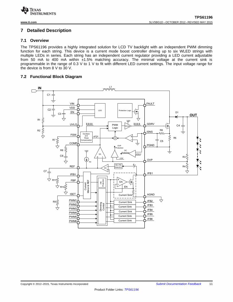
Simplified Schematic3 DescriptionThe TPS61196 provides a highly integrated solutionfor LCD TV backlight with an independent PWMdimming function for each string. This device is acurrent mode boost controller driving up to six WLEDstrings with multiple LEDs in series. Each string hasan independent current regulator providing a LEDcurrent adjustable from 50 mA to 400 mA within±1.5% matching accuracy. The minimal voltage at thecurrent sink is programmable in the range of 0.3 V to1 V to fit with different LED current settings. The inputvoltage range for the device is from 8 V to 30 V.
The device adjusts the boost controller's outputvoltage automatically to provide only the voltagerequired by the LED string with the largest forwardvoltage drop plus the minimum required voltage atthat string's IFB pin, thereby optimizing driverefficiency. Its switching frequency is programmed byan external resistor from 100 kHz to 800 kHz.
1
An IMPORTANT NOTICE at the end of this data sheet addresses availability, warranty, changes, use in safety-critical applications,intellectual property matters and other important disclaimers. PRODUCTION DATA.

TPS61196SLVSBG1D –OCTOBER 2012–REVISED MAY 2015 www.ti.com
Table of Contents7.2 Functional Block Diagram ....................................... 111 Features .................................................................. 17.3 Feature Description................................................. 122 Applications ........................................................... 17.4 Device Functional Modes........................................ 163 Description ............................................................. 1
8 Application and Implementation ........................ 194 Revision History..................................................... 28.1 Application Information............................................ 195 Pin Configuration and Functions ......................... 38.2 Typical Application ................................................. 206 Specifications......................................................... 4
9 Power Supply Recommendations ...................... 236.1 Absolute Maximum Ratings ...................................... 410 Layout................................................................... 246.2 ESD Ratings.............................................................. 4
10.1 Layout Guidelines ................................................. 246.3 Recommended Operating Conditions....................... 410.2 Layout Example .................................................... 246.4 Thermal Information .................................................. 5
11 Device and Documentation Support ................. 256.5 Electrical Characteristics........................................... 511.1 Trademarks ........................................................... 256.6 Switching Characteristics .......................................... 711.2 Electrostatic Discharge Caution............................ 256.7 Typical Characteristics .............................................. 811.3 Glossary ................................................................ 257 Detailed Description ............................................ 11
12 Mechanical, Packaging, and Orderable7.1 Overview ................................................................. 11Information ........................................................... 25
4 Revision HistoryNOTE: Page numbers for previous revisions may differ from page numbers in the current version.
Changes from Revision C (March 2013) to Revision D Page
• Added Device Information and ESD Rating tables, Feature Description, Device Functional Modes, Application andImplementation, Power Supply Recommendations, Layout, Device and Documentation Support, and Mechanical,Packaging, and Orderable Information sections; moved some curves to Application Curves section; remove DeviceComparison table.................................................................................................................................................................... 1
• Changed location of several specs from EC table to Switching Char ................................................................................... 7
Changes from Revision B (January 2013) to Revision C Page
• Changed VL max value from 1.0 V to 0.8 V ........................................................................................................................... 5• Changed VIN = 7 V to VIN = 8 V in Test Conditions for VISNS(OC) ............................................................................................ 6
Changes from Revision A (November 2012) to Revision B Page
• Changed RPD max value from 2.4 MΩ to 3.0 MΩ................................................................................................................... 5• Changed VISET min value from 1.220 V to 1.217 V ................................................................................................................ 5• Deleted IFLT_L max value......................................................................................................................................................... 6• Changed R7 to R9 in Table 1............................................................................................................................................... 12
Changes from Original (October 2012) to Revision A Page
• Changed Figure 20 .............................................................................................................................................................. 14
2 Submit Documentation Feedback Copyright © 2012–2015, Texas Instruments Incorporated
Product Folder Links: TPS61196

COMP
VDD
1
2
3
4
5
6
7
8
9
10
PGND
OVP
GDRV
ISNS
EN
PWM3
ISET
IFB2
FBP
FSW
IFB3
IFB1
VIN
11
12
13
14
28
27
26
25
24
23
22
21
20
19
18
17
16
15
PWM2
PWM1
IFBV
PWM4
PWM5
PWM6
AGND
IFB5
IFB4
IFB6
UVLO
FAULT
REF
TP
S61
196
TPS61196www.ti.com SLVSBG1D –OCTOBER 2012–REVISED MAY 2015
5 Pin Configuration and Functions
28-Pin HTSSOPPWP Package
Top View
Pin FunctionsPIN
TYPE DESCRIPTIONNUMBER NAME
Low input voltage lockout. Use a resistor divider from VIN to this pin to set the UVLO1 UVLO I threshold.2 EN I Enable and disable pin. EN high = enable, EN low = disable.3,4,5,6,7,8 PWM1 to PWM6 I PWM signal input pins. The frequency of PWM signal is in the range of 90 Hz to 22 kHz.
LED cross-short protection threshold program pin. Use a resistor to GND to set the9 FBP O threshold.Connecting a resistor to the pin programs the IFB pin current level for full brightness (that is,10 ISET O 100% dimming).
11 IFBV O Minimum feedback voltage setting for LED strings.12,13,14,15,1 IFB1 to IFB6 I Regulated current sink input pins6,1718 AGND G Analog ground
Overvoltage protection detection input. Connect a resistor divider from output to this pin to19 OVP I program the OVP threshold.20 COMP O Loop compensation for the boost converter. Connect a RC network to make loop stable.
Internal reference voltage for the boost converter. Use a capacitor at this pin to adjust the21 REF O soft start time. When two chips operate in parallel, connect the master's REF pin to the
slave's COMP pin.22 PGND G External MOSFET current sense ground input.23 ISNS I External MOSFET current sense positive input.24 GDRV o External switch MOSFET gate driver output.
Internal regulator output for device internal power supply. Connect a 1-µF ceramic capacitor25 VDD O to this pin.Switching frequency setting pin. Use a resistor to set the frequency between 100 kHz to 800
26 FSW O kHz. An external input voltage above 3.5 V or below 0.5 V disables the internal clock andmakes the device as slave device.
27 FAULT O Fault indicator. Open-drain output. Output high impedance when fault conditions happens.28 VIN I Power supply input pin
Copyright © 2012–2015, Texas Instruments Incorporated Submit Documentation Feedback 3
Product Folder Links: TPS61196

TPS61196SLVSBG1D –OCTOBER 2012–REVISED MAY 2015 www.ti.com
6 Specifications
6.1 Absolute Maximum Ratingsover operating free-air temperature range (unless otherwise noted) (1)
MIN MAX UNITVIN pin –0.3 33FAULT pin –0.3 VIN
FB1 to IFB6 pins –0.3 40FBP, ISET, ISNS, IFBV pins –0.3 3.3
Voltage (2) VEN, PWM1 to PWM6 pins –0.3 20GDRV pins –0.3 7GDRV 10-ns transient pins –2 9All other pins –0.3 7
Continuous power dissipation See Thermal InformationOperating junction temperature –40 150 °CStorage temperature, Tstg –65 150 °C
(1) Stresses beyond those listed under Absolute Maximum Ratings may cause permanent damage to the device. These are stress ratingsonly, which do not imply functional operation of the device at these or any other conditions beyond those indicated under RecommendedOperating Conditions. Exposure to absolute-maximum-rated conditions for extended periods may affect device reliability.
(2) All voltage values are with respect to network ground terminal.
6.2 ESD RatingsVALUE UNIT
Human-body model (HBM), per ANSI/ESDA/JEDEC JS-001 (1) ±2000ElectrostaticV(ESD) Charged-device model (CDM), per JEDEC specification JESD22-C101 (2) ±1000 Vdischarge
Machine model 200 (max)
(1) JEDEC document JEP155 states that 500-V HBM allows safe manufacturing with a standard ESD control process.(2) JEDEC document JEP157 states that 250-V CDM allows safe manufacturing with a standard ESD control process.
6.3 Recommended Operating Conditionsover operating free-air temperature range (unless otherwise noted) (1)
MIN NOM MAX UNITVIN Input voltage 8 30 VVOUT Output voltage VIN 120 VL1 Inductor 10 100 µHCIN Input capacitor 10 µFCOUT Output capacitor 22 220 µFfSW Boost regulator switching frequency 100 800 kHzfDIM PWM dimming frequency 0.09 22 kHzTA Operating ambient temperature –40 85 °CTJ Operating junction temperature –40 125 °C
(1) Customers need to verify the component value in their application if the values are different from the recommended values.
4 Submit Documentation Feedback Copyright © 2012–2015, Texas Instruments Incorporated
Product Folder Links: TPS61196

TPS61196www.ti.com SLVSBG1D –OCTOBER 2012–REVISED MAY 2015
6.4 Thermal InformationTPS61196
THERMAL METRIC (1) PWP UNIT28 PINS
RθJA Junction-to-ambient thermal resistance 33.8RθJC(top) Junction-to-case (top) thermal resistance 18.8RθJB Junction-to-board thermal resistance 15.6
°C/WψJT Junction-to-top characterization parameter 0.6ψJB Junction-to-board characterization parameter 15.4RθJC(bot) Junction-to-case (bottom) thermal resistance 2.5
(1) For more information about traditional and new thermal metrics, see the IC Package Thermal Metrics application report, SPRA953.
6.5 Electrical CharacteristicsVIN= 24 V, minimum and maximum limits are at TA = –40°C to +85°C, typical values are at TA = 25°C, C1 = 10 μF, C2 = 2.2μF, C3 = 1 μF, EC1 = EC2 = 100 μF (unless otherwise noted).
PARAMETER TEST CONDITIONS MIN TYP MAX UNITPOWER SUPPLYVIN Input voltage range 8 30 VVVIN_UVLO Undervoltage lockout threshold VIN falling 6.5 7 VVVIN_HYS VIN UVLO hysteresis 300 mV
Operating quiescent current into Device enabled, no switching, VIN =Iq_VIN 2 mAVIN 30 VVIN = 12 V, 25ISD Shutdown current µAVIN = 30 V 50
Regulation voltage for internalVDD 0 mA < IDD < 15 mA 5.7 6 6.3 VcircuitEN and PWMxVH Logic high input on EN,PWMx VIN = 8 V to 30 V 1.8 VVL Logic low input on EN, PWMx VIN = 8 V to 30 V 0.8 V
Pull-down resistance on EN,RPD 0.8 1.6 3 MΩPWMxUVLOVUVLOTH Threshold voltage at UVLO pin 1.204 1.229 1.253 V
VUVLO = VUVLOTH – 50 mV –0.1 a 0.1IUVLO UVLO input bias current µAVUVLO = VUVLOTH + 50 mV –4.3 -3.9 –3.3SOFT START
PWM ON, VREF< 2 V 200ISS Soft start charging current µAPWM ON, VREF> 2 V 10CURRENT REGULATIONVISET ISET pin voltage 1.217 1.229 1.240 V
ISET short-to-ground protectionIISET_P 120 150 180 µAthresholdKISET Current multiple IIFB/IISET IISET = 32.56 µA, VIFB = 0.5 V 3932 3992 4052IIFB(AVG) Current accuracy IISET = 32.56 µA, VIFB = 0.5 V 127.4 130 132.6 mA
Current matching; (IFB(MAX)-KIFB(M) IISET = 32.56 µA, VIFB = 0.5 V 0.5% 1.5%IFB(MIN))/2IFB(AVG)
IFB pin leakage current atIIFB_LEAK IFB voltage < 40 V 1 µAdimming offIIFB_max Current sink max output current VIFBV = 350 mV 130 mA
Copyright © 2012–2015, Texas Instruments Incorporated Submit Documentation Feedback 5
Product Folder Links: TPS61196

TPS61196SLVSBG1D –OCTOBER 2012–REVISED MAY 2015 www.ti.com
Electrical Characteristics (continued)VIN= 24 V, minimum and maximum limits are at TA = –40°C to +85°C, typical values are at TA = 25°C, C1 = 10 μF, C2 = 2.2μF, C3 = 1 μF, EC1 = EC2 = 100 μF (unless otherwise noted).
PARAMETER TEST CONDITIONS MIN TYP MAX UNITIFB REGULATION VOLTAGE
Measured on VIFB(min), other IFBvoltages are 0.5 V above VIFB(min).VIFB Regulation voltage at IFB 508 mVIIFB = 130 mA, VIFBV = 0.5 V
IFB Regulation voltage settingIIFBV VIFBV = 0.5 V 0.247 0.25 0.253 IISETsourcing current at IFBVVIFBV IFBV voltage setting range 0.3 1 VBOOST REFERENCE VOLTAGE
Reference voltage range forVREF 0 3.1 Vboost controllerIREF_LEAK Leakage current at REF pin –25 25 nAOSCILLATORVFSW FSW pin reference voltage 1.8 VVFSW_H Logic high input voltage 3.5 VVFSW_L Logic low input voltage 0.5 VERROR AMPLIFIERISINK Comp pin sink current VOVP = VREF + 200 mV, VCOMP = 1 V 20 µAISOURCE Comp pin source current VOVP = VREF – 200 mV, VCOMP = 1 V 20 µAGmEA Error amplifier transconductance 90 120 150 µSREA Error amplifier output resistance 20 MΩ
GATE DRIVERGate driver impedance whenRGDRV(SRC) VDD = 6 V, IGDRV = –20 mA 2 3 ΩsourcingGate driver impedance whenRGDRV(SNK) VDD = 6 V, IGDRV = 20 mA 1 1.5 Ωsinking
IGDRV(SRC) Gate driver source current VGDRV = 5 V 200 mAIGDRV(SNK) Gate driver sink current VGDRV = 1 V 400 mAVISNS(OC) Overcurrent detection threshold VIN = 8 V to 30 V, TJ = 25°C to 125°C 376 400 424 mVOVERVOLTAGE PROTECTION (OVP)VOVPTH Output voltage OVP threshold 2.95 3.02 3.09 VIOVP Leakage current –100 0 100 nAVIFB_OVP IFBx over voltage threshold PWM ON 38 VLED SHORT DETECTION
LED short detection sourcingIFBP VFBP = 1 V 0.247 0.25 0.253 IISETcurrentFAULT INDICATOR
Leakage current in highIFLT_H VFLT = 24 V 1 nAimpedanceIFLT_L Sink current at low output VFLT = 1 V 1 2 mATHERMAL SHUTDOWNTshutdown Thermal shutdown threshold 150 °C
Thermal shutdown thresholdThys 15 °Chysteresis
6 Submit Documentation Feedback Copyright © 2012–2015, Texas Instruments Incorporated
Product Folder Links: TPS61196

TPS61196www.ti.com SLVSBG1D –OCTOBER 2012–REVISED MAY 2015
6.6 Switching Characteristicsover operating free-air temperature range (unless otherwise noted)
PARAMETER TEST CONDITIONS MIN TYP MAX UNITƒSW Switching frequency RFSW = 200 kΩ 187 200 213 kHzDmax Maximum duty cycle ƒSW = 200 kHz 90% 94% 98%ton(min) Minimum pulse width 200 nsfEA Error amplifier crossover frequency 1000 kHz
Copyright © 2012–2015, Texas Instruments Incorporated Submit Documentation Feedback 7
Product Folder Links: TPS61196

4 µs/divG007
InductorCurrent1 A/div
V (AC)
200 mV/divOUT
SW50 V/div
0
100
200
300
400
500
600
700
800
900
1000
0 50 100 150 200 250 300 350 400 450LED Current (mA)
Min
imum
Hea
droo
m V
olta
ge (
mV
)
G006
0.5
0.55
0.6
0.65
0.7
0.75
0.8
0.85
0.9
0.95
1
0 200 400 600 800 1000 1200 1400 1600 1800 2000Output Current (mA)
Effi
cien
cy (
%)
VIN = 24 V, 16 LEDsVIN = 24 V, 20 LEDsVIN = 12 V, 16 LEDs
G001
0
100
200
300
400
500
600
700
800
900
0 50 100 150 200 250 300 350 400 450Resistance (kΩ)
Fre
quen
cy (
kHz)
G005
0
100
200
300
400
500
600
700
800
0 10 20 30 40 50 60 70 80 90 100
100 Hz Dimming
1 kHz Dimming
PWM Dimming Duty Cycle (%)
Tot
al L
ED
Ave
rage
Cur
rent
(m
A)
G003
0
2
4
6
8
10
12
14
16
0 0.2 0.4 0.6 0.8 1 1.2 1.4 1.6 1.8 2
100 Hz Dimming
1 kHz Dimming
PWM Dimming Duty Cycle (%)
Tot
al L
ED
Ave
rage
Cur
rent
(m
A)
G004
TPS61196SLVSBG1D –OCTOBER 2012–REVISED MAY 2015 www.ti.com
6.7 Typical Characteristics
Figure 1. Dimming Linearity Figure 2. Dimming Linearity at Low Dimming Duty Cycle
Figure 3. DC Load Efficiency Figure 4. Switching Frequency Setting
Figure 5. Recommended Minimum Headroom Voltage Figure 6. Boost Switching Waveform
8 Submit Documentation Feedback Copyright © 2012–2015, Texas Instruments Incorporated
Product Folder Links: TPS61196

2 s/divG012
ILED
100 mA/div
V
20 V/div
OUT
IFB1
10 V/div
EN
5 V/div
2 s/divG013
ILED
100 mA/div
V
20 V/div
OUT
IFB1
10 V/div
EN
5 V/div
10 µs/divG010
ILED100 mA/div
V (AC)
200 mV/divOUT
IFB110 V/div
SW50 V/div
20 µs/divG011
ILED100 mA/div
V (AC)
200 mV/divOUT
IFB110 V/div
SW50 V/div
40 ms/divG008
I
1 A/div
IN
V
20 V/div
OUT
IFB1
10 V/div
EN
5 V/div
40 ms/divG009
I
1 A/div
IN
V
20 V/div
OUT
IFB1
5 V/div
EN
5 V/div
TPS61196www.ti.com SLVSBG1D –OCTOBER 2012–REVISED MAY 2015
Typical Characteristics (continued)
1% Dimming 100% Dimming
Figure 7. Start-up Waveform Figure 8. Start-up Waveform
0.1% Dimming 2% Dimming
Figure 9. Dimming Waveform Figure 10. Dimming Waveform
1% Dimming 100% Dimming
Figure 11. Shutdown Waveform Figure 12. Shutdown Waveform
Copyright © 2012–2015, Texas Instruments Incorporated Submit Documentation Feedback 9
Product Folder Links: TPS61196

20 ms/divG018
ILED
100 mA/div
V
20 V/div
OUT
IFB1
10 V/div
Fault
5 V/div
20 ms/divG019
ILED
100 mA/div
V
20 V/div
OUT
IFB1
500 mV/div
Fault
5 V/div
2 ms/divG016
ILED
100 mA/div
V
20 V/div
OUT
IFB1
10 V/div
Fault
5 V/div
100 µs/divG017
ILED100 mA/div
V
20 V/divOUT
IFB110 V/div
Fault5 V/div
10 ms/divG014
ILED
100 mA/div
V
20 V/div
OUT
IFB1
10 V/div
Fault
5 V/div
10 ms/divG015
ILED
100 mA/div
V
20 V/div
OUT
IFB1
10 V/div
Fault
5 V/div
TPS61196SLVSBG1D –OCTOBER 2012–REVISED MAY 2015 www.ti.com
Typical Characteristics (continued)
1% Dimming 100% Dimming
Figure 13. LED Open Protection Figure 14. LED Open Protection
100% Dimming1% Dimming
Figure 16. LED Short ProtectionFigure 15. LED Short Protection
1% Dimming 100% Dimming
Figure 17. IFB Short-to-Ground Protection Figure 18. IFB Short-to-Ground Protection
10 Submit Documentation Feedback Copyright © 2012–2015, Texas Instruments Incorporated
Product Folder Links: TPS61196
VIN
Driver
PWM6
EA
EA
FSW
ISET
Curr
ent
Mirr
or&
RE
F
EN
Current Sink
Current Sink
Current Sink
Current Sink
Current Sink
Current Sink
Dim
min
g
Control
C4
R3
R4
PGND
IFB1
AGND
C1
R7
R9
OVP
Min IFB
Selection
VDD
6
PWM
Logic
Oscillatorand
Slope
Compensation
ISNS
GDRV
400mV
OC
Protection
OUT
FBP
R10
COMP
IFB
Pro
tection
LDO
C3
C6
R8
VDD
EN
L1IN
IFB2
IFB3
IFB4
IFB5
IFB6
R1
R2
UVLO
PWM2
PWM3
PWM4
PWM5
PWM1
FAULT
OVP
Protection
D1
R5
REFEA
C7
C2
R6
C5
Protection Logic
R11
IFBV
3.0V
VDD
Iss
TPS61196www.ti.com SLVSBG1D –OCTOBER 2012–REVISED MAY 2015
7 Detailed Description
7.1 OverviewThe TPS61196 provides a highly integrated solution for LCD TV backlight with an independent PWM dimmingfunction for each string. This device is a current mode boost controller driving up to six WLED strings withmultiple LEDs in series. Each string has an independent current regulator providing a LED current adjustablefrom 50 mA to 400 mA within ±1.5% matching accuracy. The minimal voltage at the current sink isprogrammable in the range of 0.3 V to 1 V to fit with different LED current settings. The input voltage range forthe device is from 8 V to 30 V.
7.2 Functional Block Diagram
Copyright © 2012–2015, Texas Instruments Incorporated Submit Documentation Feedback 11
Product Folder Links: TPS61196
( )SW
40000f kHz
R9=
TPS61196SLVSBG1D –OCTOBER 2012–REVISED MAY 2015 www.ti.com
7.3 Feature Description
7.3.1 Supply VoltageThe TPS61196 has a built-in linear regulator to supply the device analog and logic circuitry. The VDD pin, outputof the regulator, must be connected to a 1-µF bypass capacitor. VDD only has a current sourcing capability of 15mA. VDD voltage is ready after the EN pin is pulled high.
7.3.2 Boost ControllerThe TPS61196 regulates the output voltage with current mode pulse width modulation (PWM) control. Thecontrol circuitry turns on an external switch FET at the beginning of each switching cycle. The input voltage isapplied across the inductor and stores the energy as the inductor current ramps up. During this portion of theswitching cycle, the load current is provided by the output capacitor. When the inductor current rises to thethreshold set by the Error Amplifier (EA) output, the switch FET is turned off and the external Schottky diode isforward biased. The inductor transfers stored energy to replenish the output capacitor and supply the loadcurrent. This operation repeats each switching cycle. The switching frequency is programmed by an externalresistor.
A ramp signal from the oscillator is added to the current ramp to provide slope compensation, shown inFigure 23. The duty cycle of the converter is then determined by the PWM Logic block which compares the EAoutput and the slope compensated current ramp. The feedback loop regulates the OVP pin to a referencevoltage generated by the minimum voltage across the IFB pins. The output of the EA is connected to the COMPpin. An external RC compensation network must be connected to the COMP pin to optimize the feedback loopfor stability and transient response.
The TPS61196 consistently adjusts the boost output voltage to account for any changes in LED forwardvoltages. In the event that the boost controller is not able to regulate the output voltage due to the minimumpulse width (ton(min), in the Electrical Characteristics), the TPS61196 enters pulse skip mode. In this mode, thedevice keeps the power switch off for several switching cycles to prevent the output voltage from rising above theregulated voltage. This operation typically occurs in light load condition or when the input voltage is higher thanthe output voltage.
7.3.3 Switching FrequencyThe switching frequency is programmed between 100 kHz to 800 kHz by an external resistor (R9 in Figure 23).To determine the resistance by a given frequency, use the curve in Figure 4 or calculate the resistance value byEquation 1. Table 1 shows the recommended resistance values for some switching frequencies.
(1)
Table 1. Recommended Resistance Values ForSwitching Frequencies
R9 ƒSW
400 k 100 kHz200 k 200 kHz100 k 400 kHz80 k 500 kHz48 k 800 kHz
7.3.4 Enable and Undervoltage LockoutThe TPS61196 is enabled with the soft start-up when the EN pin voltage is higher than 1.8 V. A voltage of lessthan 1 V disables the device.
An undervoltage lockout (UVLO) protection feature is provided. When the voltage at the VIN pin is less than 6.5V, the TPS61196 is powered off. The TPS61196 resumes the operation once the voltage at the VIN pin recoversabove the hysteresis (VVIN_HYS) more than the UVLO threshold of input falling voltage. If a higher UVLO voltageis required, use the UVLO pin as shown in Figure 19 to adjust the input UVLO threshold by using an externalresistor divider. Once the voltage at the UVLO pin exceeds the 1.229-V threshold, the device is powered on, and
12 Submit Documentation Feedback Copyright © 2012–2015, Texas Instruments Incorporated
Product Folder Links: TPS61196

START STOP
HYS
START
V VR1 R5
I
1.229VR2 (R1 R5)
V 1.229V
-
+ =
= + ´
-
UVLO
Comparator
R5
R1
VIN
Enable
UVLO
IHYS
1.229V
R2
C4
TPS61196www.ti.com SLVSBG1D –OCTOBER 2012–REVISED MAY 2015
a hysteresis current source of 3.9 µA is added. When the voltage at the UVLO pin drops lower than 1.229 V, thecurrent source is removed. The resistors of R1, R2, and R5 can be calculated by Equation 2 from requiredVSTART and VSTOP. To avoid noise coupling, the resistor divider R1 and R2 must be close to the UVLO pin.Placing a filter capacitor of more than 10 nF as shown in Figure 19 can eliminate the impact of the switchingripple and improve the noise immunity.
If the UVLO function is not used, pull up the UVLO pin to the VDD pin.
Figure 19. Undervoltage Lockout Circuit
where• IHYS is 3.9 µA sourcing current from the UVLO pin. (2)
When the UVLO condition happens, the FAULT pin outputs high impedance. As long as the UVLO conditionremoves, the FAULT pin outputs low impedance.
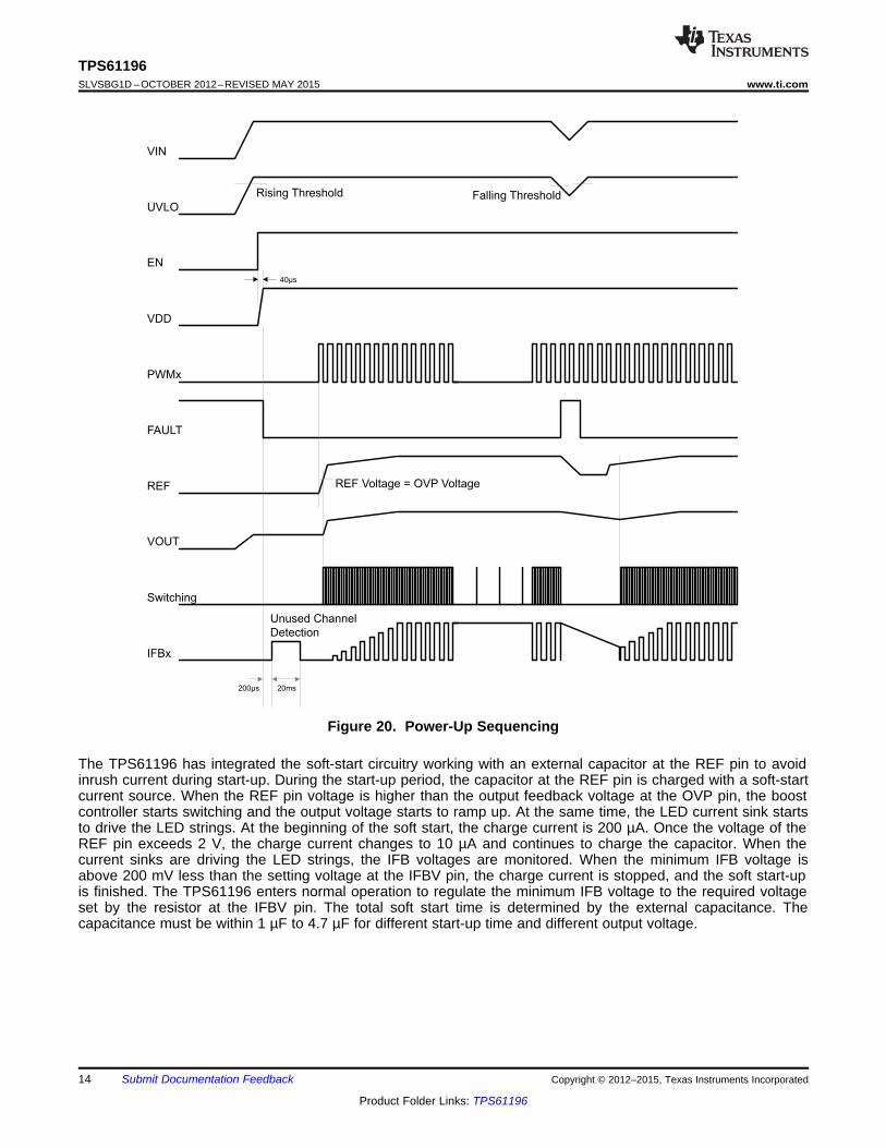
7.3.5 Power-up Sequencing and Soft Start-upThe input voltage, UVLO pin voltage, EN input signal and the input dimming PWM signal control the power up ofthe TPS61196. After the input voltage is above the required minimal input voltage of 7.5 V, the internal circuit isready to be powered up. After the UVLO pin is above the threshold of 1.229 V and the EN signal is high, theinternal LDO and logic circuit are activated. The device outputs a 20-ms pulse to detect the unused channels andremove them from the control loop. When any PWM dimming signal is high, the soft start-up begins. If the PWMdimming signals come before the EN signal is high, the soft start-up begins immediately after the detection ofunused channels.
Copyright © 2012–2015, Texas Instruments Incorporated Submit Documentation Feedback 13
Product Folder Links: TPS61196
VIN
EN
PWMx
FAULT
REF
Switching
VOUT
IFBx
UVLO
Rising Threshold
REF Voltage = OVP Voltage
Unused Channel
Detection
Falling Threshold
VDD
20ms200 sμ
40 sμ
TPS61196SLVSBG1D –OCTOBER 2012–REVISED MAY 2015 www.ti.com
Figure 20. Power-Up Sequencing
The TPS61196 has integrated the soft-start circuitry working with an external capacitor at the REF pin to avoidinrush current during start-up. During the start-up period, the capacitor at the REF pin is charged with a soft-startcurrent source. When the REF pin voltage is higher than the output feedback voltage at the OVP pin, the boostcontroller starts switching and the output voltage starts to ramp up. At the same time, the LED current sink startsto drive the LED strings. At the beginning of the soft start, the charge current is 200 µA. Once the voltage of theREF pin exceeds 2 V, the charge current changes to 10 µA and continues to charge the capacitor. When thecurrent sinks are driving the LED strings, the IFB voltages are monitored. When the minimum IFB voltage isabove 200 mV less than the setting voltage at the IFBV pin, the charge current is stopped, and the soft start-upis finished. The TPS61196 enters normal operation to regulate the minimum IFB voltage to the required voltageset by the resistor at the IFBV pin. The total soft start time is determined by the external capacitance. Thecapacitance must be within 1 µF to 4.7 µF for different start-up time and different output voltage.
14 Submit Documentation Feedback Copyright © 2012–2015, Texas Instruments Incorporated
Product Folder Links: TPS61196

( )IFBV
R10V 307.3 mV
R11= ´
ISETLED ISET
VI K
R11= ´
15ms
VIN
VOUT
UVLO
EN
200uA
Charging
Current
Dimming Off
PWM
Dimming
200ms
(VOUT = VIN – VD)
VREF=2V
10uA
Charging
Current Soft Startup Done
VIFB(min)>VIFBV – 200mV
TPS61196www.ti.com SLVSBG1D –OCTOBER 2012–REVISED MAY 2015
Figure 21. Soft-Start Waveforms
7.3.6 Unused LED StringIf the application requires less than six LED strings, the TPS61196 simply requires connecting the unused IFBpin to ground through a resistor between 20 kΩ and 36 kΩ. Once the TPS61196 is turned on, the TPS61196uses a 60-µA current source to detect the IFB pin voltage. If the IFB voltage is between 1 V and 2.5 V, thedevice immediately disables this string during start-up.
7.3.7 Current RegulationThe six channel current sink regulators can be configured to provide up to 400 mA per string. The expected LEDcurrent is programmed by a resistor (R11 in Figure 23) at the ISET using Equation 3.
where• VISET is the ISET pin voltage of 1.229 V• KISET is the current multiple of 3992. (3)
To sink the set LED current, the current sink regulator requires a minimum headroom voltage at the IFB pins forworking properly. For example, when the LED current is set to 130 mA, the minimum voltage required at the IFBpin must be higher than 0.35 V. For other LED currents, refer to Figure 5 for recommended minimum headroomvoltage required. The TPS61196 regulates the minimum voltage of the IFB pins to the IFBV voltage. The IFBVvoltage is adjustable with an external resistor (R10 in the Figure 23) at the IFBV pin. After choosing the minimumIFB voltage, the IFBV voltage must be set to this value and the setting resistance can be calculated byEquation 4.
(4)
If a large LED current is set, the headroom voltage is required higher. This leads to more heat on the device. Tomaintain the total power dissipation in the range of the package limit, normally all strings can not sink largecurrent in continuous mode but pulse mode. The backlight of an active shutter glass 3-D TV may work with largeLED current in pulse mode.
Copyright © 2012–2015, Texas Instruments Incorporated Submit Documentation Feedback 15
Product Folder Links: TPS61196

LED _ SHORT
R12V 1.229V
R11= ´
TPS61196SLVSBG1D –OCTOBER 2012–REVISED MAY 2015 www.ti.com
7.3.8 PWM DimmingLED brightness dimming is set by applying an external PWM signal of 90 Hz to 22 kHz to the PWM pins. EachLED string has an independent PWM input. Varying the PWM duty cycle from 0% to 100% adjusts the LED fromminimum to maximum brightness respectively. The recommended minimum on time of the LED string is 10 µsec.Thus, the device has a minimum dimming duty cycle of 500:1 at 200 Hz.
When all PWM voltages are pulled low during dimming off, the TPS61196 turns off the LED strings and keepsthe boost converter running at PFM mode. The output voltage is kept at the level which is a little bit lower thanthat when PWM is high. Thus, the device limits the output ripple due to the load transient that occurs duringPWM dimming.
When all PWM voltages are pulled low for more than 20 ms, to avoid the REF pin voltage dropping due to theleakage current, the voltage of the REF pin is held by an internal reference voltage which equals to the REF pinvoltage in normal dimming operation. Thus, the output voltage will be kept at the same level as the normal outputvoltage.
Since the output voltage in long time dimming off status is almost the same as the normal voltage for turning theLED on, the TPS61196 turns on the LED very fast without any flicker when recovering from long time dimmingoff to small duty cycle dimming on.
7.4 Device Functional Modes
7.4.1 ProtectionsThe TPS61196 has a full set of protections making the system safe to any abnormal conditions. Someprotections will latch the TPS61196 in off state until its power supply is recycled or it is disabled and thenenabled again. In latch off state, the REF pin voltage is discharged to 0 V.
7.4.1.1 Switch Current Limit Protection Using the ISNS PinThe TPS61196 monitors the inductor current through the voltage across a sense resistor (R7 in the Figure 23) inorder to provide current limit protection. During the switch FET on period, when the voltage at the ISNS pin risesabove 400 mV (VISNS in the Electrical Characteristics table), the TPS61196 turns off the FET immediately anddoes not turn it back on until the next switch cycle. The switch current limit is equal to 400 mV / R7.
7.4.1.2 LED Open ProtectionWhen one of the LED strings is open, the voltage at the IFB pin connecting to this LED string drops to zeroduring dimming-on time. The TPS61196 monitors the IFB voltage for 20 ms. If the IFB voltage is still below thethreshold of 0.2 V, the current sink is disabled and an internal pull-up current is activated to detect the IFBvoltage again. If the IFB voltage is pulled up to a high voltage, this LED string is recognized as LED open. As aresult, the device deactivates the open IFB pin and removes it from the voltage feedback loop. Afterwards, theoutput voltage returns to the voltage required for the connected LED strings. The IFB pin currents of theconnected strings remain in regulation during this process. If all the LED strings are open, the TPS61196 islatched off.
7.4.1.3 LED Short-Cross Protection Using the FBP PinIf one or several LEDs short in one string, the corresponding IFB pin voltage rises but continues to sink the LEDcurrent, causing increased device power dissipation. To protect the device, the TPS61196 provides aprogrammable LED short-across protection feature by properly sizing the resistor on the FBP pin (R12 inFigure 23) using Equation 5.
(5)
If any IFB pin voltage exceeds the threshold (VLED_SHORT), the device turns off the corresponding current sink andremoves this IFB pin from the output voltage regulation loop. Current regulation of the remaining IFB pins is notaffected.
16 Submit Documentation Feedback Copyright © 2012–2015, Texas Instruments Incorporated
Product Folder Links: TPS61196

OVPVR3 1 R4
3.02
æ ö= - ´ç ÷
è ø
TPS61196www.ti.com SLVSBG1D –OCTOBER 2012–REVISED MAY 2015
Device Functional Modes (continued)7.4.1.4 Schottky Diode Open ProtectionWhen the device is powered on, it checks the topology connection first. After the TPS61196 delays 400 µs, itchecks the voltage at the OVP pin to see if the Schottky diode is not connected or the boost output is hard-shorted to ground. If the voltage at the OVP pin is lower than 70 mV, the TPS61196 is locked in off state until theinput power is recycled or it is enabled again.
7.4.1.5 Schottky Diode Short ProtectionIf the rectifier Schottky diode is shorted, the reverse current from output capacitor to ground is very large whenthe switcher MOSFET is turned on. Because the current mode control topology has a minimum edge blankingtime to immunize against the spike current through the switcher, if the parasite inductance between the outputcapacitor through the switcher to ground is zero, the external MOSFET will be damaged in this short period dueto the huge power dissipation in this case. But with a small parasite inductance, the power dissipation is limited.The boost converter works in minimum pulse width in this situation due to cycle by cycle over-current protection.The output voltage drops and the all-string-open protection is triggered because of the low voltage at all IFB pins.The TPS61196 is latched off.
7.4.1.6 IFB Overvoltage Protection During Start-upWhen any of IFB pins reaches the threshold (VOVP_IFB) of 38 V during start-up, the device stops switching andstays in latch-off immediately to protect from damage. In latch-off state, the REF pin voltage is discharged.
7.4.1.7 Output Overvoltage Protection Using the OVP PinUse a resistor divider to program the maximum output voltage of the boost converter. To ensure the LED stringcan be turned on with setting current, the maximum output voltage must be higher than the forward voltage dropof the LED string. The maximum required voltage can be calculated by multiplying the maximum LED forwardvoltage (VFWD(max)) and number (n) of series LEDs , and adding extra 1 V to account for regulation and resistortolerances and load transients.
The recommended bottom feedback resistor of the resistor divider (R4 in Figure 23) is 10 kΩ. Calculate the topresistor (R3 in the Figure 23) using Equation 6, where VOVP is the maximum output voltage of the boostconverter.
(6)
When the device detects that the voltage at the OVP pin exceeds overvoltage protection threshold of 3.02 V,indicating that the output voltage has exceeded the clamp threshold voltage, the TPS61196 clamps the outputvoltage to the set threshold. When the OVP pin voltage does not drop from the OVP threshold for more than 500ms, the device is latched off until the input power or the EN pin voltage is re-cycled.
7.4.1.8 Output Short-to-Ground ProtectionWhen the inductor peak current reaches twice the switch current limit in each switching cycle, the deviceimmediately disables the boost controller until the fault is cleared. This protects the device and externalcomponents from damage if the output is shorted to ground.
7.4.1.9 IFB Short-to-Ground ProtectionThe IFB pin short to ground makes the LED current uncontrollable if there is no protection. If the device tries toincrease the boost converter’s output voltage to lift the IFB voltage, it will make the situation worse and the LEDstring may be burned due to the high current. The TPS61196 implements a protection mechanism to protect theLED string in this failure mode.
If the IFB is short to ground before the TPS61196 is turned on, the device detects the IFB voltage by sourcing a60 µA current during start-up. If the IFB voltage is less than 0.4 V during start-up, the start-up stops and thedevice outputs fault indication so as to protect the LED string during start-up.
Copyright © 2012–2015, Texas Instruments Incorporated Submit Documentation Feedback 17
Product Folder Links: TPS61196

TPS61196SLVSBG1D –OCTOBER 2012–REVISED MAY 2015 www.ti.com
Device Functional Modes (continued)When a LED feedback pin is shorted to ground during normal operation, the device first turns off this LED stringfor a very short time and detects the IFB voltage again. If the IFB voltage is lower than 1.8 V, it sources a 60-µAcurrent and detects the IFB voltage again in off state. If the IFB voltage is still less than 1.8 V, this means the IFBpin is shorted to ground. The boost converter is turned off and the REF voltage is discharged to ground to protectthe LED string.
7.4.1.10 ISET Short-to-Ground ProtectionThe TPS61196 monitors the ISET pin voltage when the device is enabled. When the sourcing current from theISET pin is larger than a threshold of 150 μA, the device disables the current sink because the ISET pin may beshort to ground or the current setting resistor is too small. Once the current sourcing from the ISET pin recoversto the normal value, the current sink resumes working.
7.4.1.11 Thermal ProtectionWhen the device junction temperature is over 150°C, the thermal protection circuit is triggered and shuts downthe device immediately. The device automatically restarts when the junction temperature falls back to less than135°C, with approximate 15°C hysteresis.
Table 2. Protection ListPROTECTION ITEM RESULT FAULT LATCH OFF / RETRY
Diode open Cannot start up Y Latch offDiode short Output voltage low Y Latch offLED string open LED string off Y LED string latch offLED string short during start-up IFB OVP Y Latch offLEDshort LED string off Y LED string latch offIFB short to GND Boost off Y Latch offISET short to GND All LED strings off Y RetryAll LED strings open during start-up VOUT OVP Y Latch offInput voltage UVLO Boost off Y RetryThermal shutdown Shutdown Y Retry
7.4.2 Indication For Fault ConditionsThe TPS61196 has an open-drain fault indicator pin to indicate abnormal conditions. When the device isoperating normally, the voltage at the FAULT pin is low. When any fault condition happens, it is in highimpedance, which can be pulled to high level through an external resistor. The FAULT pin can indicate followingconditions:• Overvoltage condition at the OVP or the IFB pin• LED short and open• IFB short to ground• ISET short to ground• Diode open and short• Output short circuit• Overtemperature
18 Submit Documentation Feedback Copyright © 2012–2015, Texas Instruments Incorporated
Product Folder Links: TPS61196

L1
68uH D1
IFB1
IFB6
ISNS
VIN
VDD
ISETAGND
TPS61196
MASTER
GDRV
FSW
C1
10 Fμ
PWM1
8V to 30V
R3
OVP
R14
EN
R8
R6
C6
C5PGND
COMP
FBP
C2
2.2μF
R7
…...
UVLO
PWM6
…...
FAULT
R10
C3
1.0 Fμ
R9
R11
REF
R1
R2
IFB1
IFB6
ISNS
VIN
VDD
ISETAGND
TPS61196
SLAVE
GDRV
FSW
PWM1
OVP
EN
PGND
COMP
FBP
…...
UVLO
PWM6
…...
FAULT
REF
8V to 30V
IFBV
R12
IFBV
C7
R4
R13
VDD
R15
EC2
C4
10nF
R5
EC1
100μF 100μF
TPS61196www.ti.com SLVSBG1D –OCTOBER 2012–REVISED MAY 2015
8 Application and Implementation
NOTEInformation in the following applications sections is not part of the TI componentspecification, and TI does not warrant its accuracy or completeness. TI’s customers areresponsible for determining suitability of components for their purposes. Customers shouldvalidate and test their design implementation to confirm system functionality.
8.1 Application InformationWhen more LED strings are required in the application, the TPS61196 can work in master/slave mode. TheTPS61196 can be set as slave device when the voltage at the FSW pin is below 0.5 V or above 3.5 V. Themaster TPS61196 has booster controller and outputs the power rail for all LED strings. The slave TPS61196 onlyworks as a LED driver and feedbacks the required headroom voltage to the master by connecting the slave'sCOMP pin to the master's REF pin. The ISNS pin of the slave TPS61196 must be connected to ground. Theslave's OVP pin voltage must be 3% higher than the voltage at the master's OVP pin. The slave device cancombine all fault conditions happening on both master and slave devices by connecting the master's FAULToutput to the FSW pin of the slave device. The slave’s FAULT pin outputs the indication signal for all faultconditions.
Figure 22. Multi-Chip Operation In Parallel
Copyright © 2012–2015, Texas Instruments Incorporated Submit Documentation Feedback 19
Product Folder Links: TPS61196

OUT OUTL(DC)
IN
V II =
V η
´
´
L1
68mH D1
IFB1
ISNS
VIN
VDD
ISET
AGND
TPS61196
GDRV
FSW
C1
10mF
PWM2
VIN = 24V
OVP
R3
EN
R19
R6
C6
C5PGND
COMP
FBP
R7
UVLO
PWM5
FAULT
R12
C31.0 Fm
R9
R11
REF
R1
R2
100mF
C7
IFBV
R10
C2
2.2mF
C9
200k
2.2mF
37.4k
196k
60.4k 0.1mF
Thermal pad
PWM6
PWM3
PWM4
PWM1IFB2
IFB6
150k
47nF
C8
R4
Q1
160pF
C410nF
R8
3
0.1
470pF
200
255k
10k
EC2EC1
100mF
182k
24.9k
IFB3
IFB4
IFB5
R1310M
R1410M
R1510M
R1610M
R1710M
R1810M
R5
200k
TPS61196SLVSBG1D –OCTOBER 2012–REVISED MAY 2015 www.ti.com
8.2 Typical Application
Figure 23. TPS61196 Typical Application
8.2.1 Design Requirements
8.2.1.1 Design Requirements
DESIGN PARAMETER EXAMPLE VALUEInput voltage range 10 V – 15 V
LED forward voltage range 56 V - 64 VNumber of LED strings × number of LEDs per string 6 x 20
LED string current 150 mA per channelSwitching frequency 500 kHz
8.2.2 Detailed Design Procedure
8.2.2.1 Inductor SelectionThe inductor is the most important component in switching power regulator design because it affects powersupply steady state operation, transient behavior, and loop stability. The inductor value, DC resistance (DCR),and saturation current are important specifications to be considered for better performance. Although the boostpower stage can be designed to operate in discontinuous mode at maximum load, where the inductor currentramps down to zero during each switching cycle, most applications will be more efficient if the power stageoperates in continuous conduction mode, where a DC current flows through the inductor. Therefore, theEquation 8 and Equation 9 below are for CCM operation only. The TPS61196 is designed to work with inductorvalues between 10 µH and 100 µH, depending on the switching frequency. Running the controller at higherswitching frequencies allows the use of smaller and/or lower profile inductors in the 10-µH range. Running thecontroller at slower switching frequencies requires the use of larger inductors, near 100 µH, to maintain the sameinductor current ripple but may improve overall efficiency due to smaller switching losses. Inductor values canhave ±20% tolerance with no current bias. When the inductor current approaches saturation level, its inductancecan decrease 20% to 35% from the 0-A value depending on how the inductor vendor defines saturation.
In a boost regulator, the inductor DC current can be calculated with Equation 7.
where• VOUT = boost output voltage• IOUT = boost output current
20 Submit Documentation Feedback Copyright © 2012–2015, Texas Instruments Incorporated
Product Folder Links: TPS61196

L(P P)L(P) L(DC)
II = I +
2
-D
( )IN OUT INL(P P)
SW OUT
V V VI =
L f V-
´ -D
´ ´
TPS61196www.ti.com SLVSBG1D –OCTOBER 2012–REVISED MAY 2015
• VIN = boost input voltage• η = power conversion efficiency, use 95% for TPS61196 applications (7)
The inductor current peak-to-peak ripple can be calculated with Equation 8.
where• ΔIL(P-P) = inductor ripple current• L = inductor value• fSW = switching frequency• VOUT = boost output voltage• VIN = boost input voltage (8)
Therefore, the inductor peak current is calculated with Equation 9.
(9)
Select an inductor, which saturation current is higher than calculated peak current. To calculate the worst-caseinductor peak current, use the minimum input voltage, maximum output voltage, and maximum load current.
Regulator efficiency is dependent on the resistance of its high current path and switching losses associated withthe switch FET and power diode. Besides the external switch FET, the overall efficiency is also affected by theinductor DCR. Usually the lower DC resistance shows higher efficiency. However, there is a trade-off betweenDCR and the inductor footprint; furthermore, shielded inductors typically have higher DCR than unshielded ones.
8.2.2.2 Schottky DiodeThe TPS61196 demands a high-speed rectification for optimum efficiency. Ensure that the diode's average andpeak current rating exceed the output LED current and inductor peak current. In addition, the diode's reversebreakdown voltage must exceed the application output voltage.
8.2.2.3 Switch MOSFET and Gate Driver ResistorThe TPS61196 demands a power N-MOSFET (see Q1 in the Figure 23) as a switch. The voltage and currentrating of the MOSFET must be higher than the application output voltage and the inductor peak current. Theapplications benefit from the addition of a resistor (See R19 in the Figure 23) connected between the GDRV pinand the gate of the switch MOSFET. With this resistor, the gate driving current is limited and the EMIperformance is improved. A 3-Ω resistor value is recommended. The TPS61196 exhibits lower efficiency whenthe resistor value is above 3 Ω due to the more switching loss of the external MOSFET.
8.2.2.4 Current Sense and Current Sense FilteringR7 determines the correct overcurrent limit protection. To choose the right value of R7, start with the total systempower needed POUT, and calculate the input current IIN by Equation 7. Efficiency can be estimated between 90%to 95%. The second step is to calculate the inductor peak current based on the inductor value L using Equation 8and Equation 9. The maximum R7 can now be calculated as R7(max) = VISNS / IL(P). It is recommended to add20% or more margins to account for component variations. A small filter placed on the ISNS pin improvesperformance of the converter (See R6 and C5 in Figure 23). The time constant of this filter should beapproximately 100 ns. The range of R6 should be from about 100 Ω to 1 kΩ for best results. The C5 should belocated as close as possible to the ISNS pin to provide noise immunity.
Copyright © 2012–2015, Texas Instruments Incorporated Submit Documentation Feedback 21
Product Folder Links: TPS61196

( )2 co OUT OVP
EA OVPTH
R7 f C VR8 =
1 D Gm V
´ ´´
- ´
π
( )2
OUT
ZRHP
OUT
V 1 Df =
2 L I
´ -
´π
OUTP
OUT OUT
2If =
2 V C´π
RIPPLE(ESR) L(P)V = I ESR´
OUT MAXRIPPLE(C)
SW OUT
I DV =
f C
´
´
TPS61196SLVSBG1D –OCTOBER 2012–REVISED MAY 2015 www.ti.com
8.2.2.5 Output CapacitorThe output capacitor is mainly selected to meet the requirements for output ripple and loop stability of the wholesystem. This ripple voltage is related to the capacitance of the capacitor and its equivalent series resistance(ESR). Assuming a capacitor with zero ESR, the minimum capacitance needed for a given ripple can becalculated by:
where• VRIPPLE is the peak to peak output voltage ripple• DMAX is the duty cycle of the boost converter. (10)
DMAX is approximately equal to (VOUT(MAX) – VIN(MIN) / VOUT(MAX)) in applications. Care must be taken whenevaluating a capacitor’s derating under DC bias. The DC bias can also significantly reduce capacitance. Ceramiccapacitors can loss as much as 50% of its capacitance at its rated voltage. Therefore, leave the margin on thevoltage rating to ensure adequate capacitance.
The ESR impact on the output ripple must be considered as well if tantalum or aluminum electrolytic capacitorsare used. Assuming there is enough capacitance such that the ripple due to the capacitance can be ignored, theESR needed to limit the VRIPPLE is:
(11)
Ripple current flowing through a capacitor’s ESR causes power dissipation in the capacitor. This powerdissipation causes a temperature increase internally to the capacitor. Excessive temperature can seriouslyshorten the expected life of a capacitor. Capacitors have ripple current ratings that are dependent on ambienttemperature and should not be exceeded. Therefore, high ripple current type electrolytic capacitor with smallESR is used in typical application as shown in Figure 23.
In the typical application, the output requires a capacitor in the range of 22 µF to 220 µF. The output capacitoraffects the small signal control loop stability of the boost converter. If the output capacitor is below the range, theboost regulator may potentially become unstable.
8.2.2.6 Loop ConsiderationThe COMP pin on the TPS61196 is used for external compensation, allowing the loop response to be optimizedfor each application. The COMP pin is the output of the internal trans-conductance amplifier. The externalresistor R8, along with ceramic capacitors C6 and C8 (see in Figure 23), are connected to the COMP pin toprovide poles and zero. The poles and zero, along with the inherent pole and zero in a peak current modecontrol boost converter, determine the closed loop frequency response. This is important to converter stabilityand transient response.
The first step is to calculate the pole and the right half plane zero of the peak current mode boost converter byEquation 12 and Equation 13.
(12)
(13)
To make the loop stable, the loop must have sufficient phase margin at the crossover frequency where the loopgain is 1. To avoid the effect of the right half plane zero on the loop stability, choose the crossover frequencyless than 1/5 of the ƒZRHP. Then calculate the compensation components by Equation 14 and Equation 15.
where• VOVPTH = 3.02 V which is the internal reference for the output overvoltage-protection setting voltage.• GmEA is the trans-conductance of the error amplifier. Its typical value is 120 μS.• ƒCO is the crossover frequency, which normally is less than 1/5 of the fZRHP (14)
22 Submit Documentation Feedback Copyright © 2012–2015, Texas Instruments Incorporated
Product Folder Links: TPS61196

0.5
0.55
0.6
0.65
0.7
0.75
0.8
0.85
0.9
0.95
1
0 10 20 30 40 50 60 70 80 90 100
PWM Dimming Duty Cycle (%)
Effic
iency (
%)
VIN = 12 V
VIN = 24 V
20 LEDs (VOUT = 60 V)
200 Hz Dimming Frequency
G001
0.5
0.55
0.6
0.65
0.7
0.75
0.8
0.85
0.9
0.95
1
0 10 20 30 40 50 60 70 80 90 100
PWM Dimming Duty Cycle (%)
Effic
ien
cy (
%)
VIN = 12 V
VIN = 24 V
16 LEDs (VOUT = 50 V)
200 Hz Dimming Frequency
G002
OUT ESRC RC8 =
R8
´
1
P
C6 =2 f R8´π
TPS61196www.ti.com SLVSBG1D –OCTOBER 2012–REVISED MAY 2015
where• ƒP is the pole’s frequency of the power stage calculated by Equation 12 (15)
If the output capacitor is the electrolytic capacitor, which may have large ESR, a capacitor is required to cancelthe zero of the output capacitor. Equation 16 calculates the value of this capacitor.
(16)
8.2.3 Application Curves
20 LEDs 16 LEDs
Figure 24. Efficiency Figure 25. Efficiency
9 Power Supply RecommendationsThe TPS61196 requires a single supply input voltage. This voltage can range between 8 V to 30 V and be ableto supply enough current for a given application.
Copyright © 2012–2015, Texas Instruments Incorporated Submit Documentation Feedback 23
Product Folder Links: TPS61196

D1
AGND
COMP
VDD
1
2
3
4
5
6
7
8
9
10
PGND
OVP
ISNS
EN
PWM3
ISET
IFB2
FBP
FSW
IFB3
IFB1
VIN
11
12
13
14
28
27
26
25
24
23
21
20
19
17
16
15
PWM2
PWM1
IFBV
PWM4
PWM5
PWM6
IFB5
IFB4
IFB6
FAULT
REF
TP
S6
11
96
GDRV
UVLO
18
22
VINGND
GND
VOUTBottom GND Plane
GND
GND
GND
TPS61196SLVSBG1D –OCTOBER 2012–REVISED MAY 2015 www.ti.com
10 Layout
10.1 Layout GuidelinesAs for all switching power supplies, especially those providing high current and using high switching frequencies,layout is an important design step. If layout is not carefully done, the regulator could show instability as well asEMI problems. Therefore, use wide and short traces for high current paths. The VDD capacitor, C3 (seeFigure 23) is the filter and noise decoupling capacitor for the internal linear regulator powering the internal digitalcircuits. It should be placed as close as possible between the VDD and PGND pins to prevent any noise insertionto digital circuits. The switch node at the drain of Q1 carries high current with fast rising and falling edges.Therefore, the connection between this node to the inductor and the schottky diode should be kept as short andwide as possible. It is also beneficial to have the ground of the capacitor C3 close to the ground of the currentsense resistor R7 since there is large driving current flowing between them. The ground of output capacitor EC2should be kept close to input power ground or through a large ground plane because of the large ripple currentreturning to the input ground. When laying out signal grounds, it is recommended to use short traces separatefrom power ground traces and connect them together at a single point, for example on the thermal pad in thePWP package. Resistors R3, R4, R9, R10, R11, and R12 (see Figure 23) are setting resistors for switchingfrequency, LED current, protection threshold and feedback voltage programming. To avoid unexpected noisecoupling into the pins and affecting the accuracy, these resistors need to be close to the pins with short and widetraces to GND. In the PWP package, the thermal pad needs to be soldered to the large ground plane on the PCBfor better thermal performance. Additional thermal via can significantly improve power dissipation of the device.
10.2 Layout Example
Figure 26. Layout Example
24 Submit Documentation Feedback Copyright © 2012–2015, Texas Instruments Incorporated
Product Folder Links: TPS61196

TPS61196www.ti.com SLVSBG1D –OCTOBER 2012–REVISED MAY 2015
11 Device and Documentation Support
11.1 TrademarksPowerPAD is a trademark of Texas Instruments.All other trademarks are the property of their respective owners.
11.2 Electrostatic Discharge CautionThese devices have limited built-in ESD protection. The leads should be shorted together or the device placed in conductive foamduring storage or handling to prevent electrostatic damage to the MOS gates.
11.3 GlossarySLYZ022 — TI Glossary.
This glossary lists and explains terms, acronyms, and definitions.
12 Mechanical, Packaging, and Orderable InformationThe following pages include mechanical, packaging, and orderable information. This information is the mostcurrent data available for the designated devices. This data is subject to change without notice and revision ofthis document. For browser-based versions of this data sheet, refer to the left-hand navigation.
Copyright © 2012–2015, Texas Instruments Incorporated Submit Documentation Feedback 25
Product Folder Links: TPS61196

PACKAGE OPTION ADDENDUM
www.ti.com 21-Oct-2014
Addendum-Page 1
PACKAGING INFORMATION
Orderable Device Status(1)
Package Type PackageDrawing
Pins PackageQty
Eco Plan(2)
Lead/Ball Finish(6)
MSL Peak Temp(3)
Op Temp (°C) Device Marking(4/5)
Samples
TPS61196PWPR ACTIVE HTSSOP PWP 28 2000 Green (RoHS& no Sb/Br)
CU NIPDAU Level-2-260C-1 YEAR -40 to 85 TPS61196
TPS61196PWPT ACTIVE HTSSOP PWP 28 250 Green (RoHS& no Sb/Br)
CU NIPDAU Level-2-260C-1 YEAR -40 to 85 TPS61196
(1) The marketing status values are defined as follows:ACTIVE: Product device recommended for new designs.LIFEBUY: TI has announced that the device will be discontinued, and a lifetime-buy period is in effect.NRND: Not recommended for new designs. Device is in production to support existing customers, but TI does not recommend using this part in a new design.PREVIEW: Device has been announced but is not in production. Samples may or may not be available.OBSOLETE: TI has discontinued the production of the device.
(2) Eco Plan - The planned eco-friendly classification: Pb-Free (RoHS), Pb-Free (RoHS Exempt), or Green (RoHS & no Sb/Br) - please check http://www.ti.com/productcontent for the latest availabilityinformation and additional product content details.TBD: The Pb-Free/Green conversion plan has not been defined.Pb-Free (RoHS): TI's terms "Lead-Free" or "Pb-Free" mean semiconductor products that are compatible with the current RoHS requirements for all 6 substances, including the requirement thatlead not exceed 0.1% by weight in homogeneous materials. Where designed to be soldered at high temperatures, TI Pb-Free products are suitable for use in specified lead-free processes.Pb-Free (RoHS Exempt): This component has a RoHS exemption for either 1) lead-based flip-chip solder bumps used between the die and package, or 2) lead-based die adhesive used betweenthe die and leadframe. The component is otherwise considered Pb-Free (RoHS compatible) as defined above.Green (RoHS & no Sb/Br): TI defines "Green" to mean Pb-Free (RoHS compatible), and free of Bromine (Br) and Antimony (Sb) based flame retardants (Br or Sb do not exceed 0.1% by weightin homogeneous material)
(3) MSL, Peak Temp. - The Moisture Sensitivity Level rating according to the JEDEC industry standard classifications, and peak solder temperature.
(4) There may be additional marking, which relates to the logo, the lot trace code information, or the environmental category on the device.
(5) Multiple Device Markings will be inside parentheses. Only one Device Marking contained in parentheses and separated by a "~" will appear on a device. If a line is indented then it is a continuationof the previous line and the two combined represent the entire Device Marking for that device.
(6) Lead/Ball Finish - Orderable Devices may have multiple material finish options. Finish options are separated by a vertical ruled line. Lead/Ball Finish values may wrap to two lines if the finishvalue exceeds the maximum column width.
Important Information and Disclaimer:The information provided on this page represents TI's knowledge and belief as of the date that it is provided. TI bases its knowledge and belief on informationprovided by third parties, and makes no representation or warranty as to the accuracy of such information. Efforts are underway to better integrate information from third parties. TI has taken andcontinues to take reasonable steps to provide representative and accurate information but may not have conducted destructive testing or chemical analysis on incoming materials and chemicals.TI and TI suppliers consider certain information to be proprietary, and thus CAS numbers and other limited information may not be available for release.

PACKAGE OPTION ADDENDUM
www.ti.com 21-Oct-2014
Addendum-Page 2
In no event shall TI's liability arising out of such information exceed the total purchase price of the TI part(s) at issue in this document sold by TI to Customer on an annual basis.

TAPE AND REEL INFORMATION
*All dimensions are nominal
Device PackageType
PackageDrawing
Pins SPQ ReelDiameter
(mm)
ReelWidth
W1 (mm)
A0(mm)
B0(mm)
K0(mm)
P1(mm)
W(mm)
Pin1Quadrant
TPS61196PWPR HTSSOP PWP 28 2000 330.0 16.4 6.9 10.2 1.8 12.0 16.0 Q1
TPS61196PWPT HTSSOP PWP 28 250 180.0 16.4 6.9 10.2 1.8 12.0 16.0 Q1
PACKAGE MATERIALS INFORMATION
www.ti.com 2-Sep-2015
Pack Materials-Page 1

*All dimensions are nominal
Device Package Type Package Drawing Pins SPQ Length (mm) Width (mm) Height (mm)
TPS61196PWPR HTSSOP PWP 28 2000 367.0 367.0 38.0
TPS61196PWPT HTSSOP PWP 28 250 213.0 191.0 55.0
PACKAGE MATERIALS INFORMATION
www.ti.com 2-Sep-2015
Pack Materials-Page 2

IMPORTANT NOTICE
Texas Instruments Incorporated and its subsidiaries (TI) reserve the right to make corrections, enhancements, improvements and otherchanges to its semiconductor products and services per JESD46, latest issue, and to discontinue any product or service per JESD48, latestissue. Buyers should obtain the latest relevant information before placing orders and should verify that such information is current andcomplete. All semiconductor products (also referred to herein as “components”) are sold subject to TI’s terms and conditions of salesupplied at the time of order acknowledgment.TI warrants performance of its components to the specifications applicable at the time of sale, in accordance with the warranty in TI’s termsand conditions of sale of semiconductor products. Testing and other quality control techniques are used to the extent TI deems necessaryto support this warranty. Except where mandated by applicable law, testing of all parameters of each component is not necessarilyperformed.TI assumes no liability for applications assistance or the design of Buyers’ products. Buyers are responsible for their products andapplications using TI components. To minimize the risks associated with Buyers’ products and applications, Buyers should provideadequate design and operating safeguards.TI does not warrant or represent that any license, either express or implied, is granted under any patent right, copyright, mask work right, orother intellectual property right relating to any combination, machine, or process in which TI components or services are used. Informationpublished by TI regarding third-party products or services does not constitute a license to use such products or services or a warranty orendorsement thereof. Use of such information may require a license from a third party under the patents or other intellectual property of thethird party, or a license from TI under the patents or other intellectual property of TI.Reproduction of significant portions of TI information in TI data books or data sheets is permissible only if reproduction is without alterationand is accompanied by all associated warranties, conditions, limitations, and notices. TI is not responsible or liable for such altereddocumentation. Information of third parties may be subject to additional restrictions.Resale of TI components or services with statements different from or beyond the parameters stated by TI for that component or servicevoids all express and any implied warranties for the associated TI component or service and is an unfair and deceptive business practice.TI is not responsible or liable for any such statements.Buyer acknowledges and agrees that it is solely responsible for compliance with all legal, regulatory and safety-related requirementsconcerning its products, and any use of TI components in its applications, notwithstanding any applications-related information or supportthat may be provided by TI. Buyer represents and agrees that it has all the necessary expertise to create and implement safeguards whichanticipate dangerous consequences of failures, monitor failures and their consequences, lessen the likelihood of failures that might causeharm and take appropriate remedial actions. Buyer will fully indemnify TI and its representatives against any damages arising out of the useof any TI components in safety-critical applications.In some cases, TI components may be promoted specifically to facilitate safety-related applications. With such components, TI’s goal is tohelp enable customers to design and create their own end-product solutions that meet applicable functional safety standards andrequirements. Nonetheless, such components are subject to these terms.No TI components are authorized for use in FDA Class III (or similar life-critical medical equipment) unless authorized officers of the partieshave executed a special agreement specifically governing such use.Only those TI components which TI has specifically designated as military grade or “enhanced plastic” are designed and intended for use inmilitary/aerospace applications or environments. Buyer acknowledges and agrees that any military or aerospace use of TI componentswhich have not been so designated is solely at the Buyer's risk, and that Buyer is solely responsible for compliance with all legal andregulatory requirements in connection with such use.TI has specifically designated certain components as meeting ISO/TS16949 requirements, mainly for automotive use. In any case of use ofnon-designated products, TI will not be responsible for any failure to meet ISO/TS16949.
Products ApplicationsAudio www.ti.com/audio Automotive and Transportation www.ti.com/automotiveAmplifiers amplifier.ti.com Communications and Telecom www.ti.com/communicationsData Converters dataconverter.ti.com Computers and Peripherals www.ti.com/computersDLP® Products www.dlp.com Consumer Electronics www.ti.com/consumer-appsDSP dsp.ti.com Energy and Lighting www.ti.com/energyClocks and Timers www.ti.com/clocks Industrial www.ti.com/industrialInterface interface.ti.com Medical www.ti.com/medicalLogic logic.ti.com Security www.ti.com/securityPower Mgmt power.ti.com Space, Avionics and Defense www.ti.com/space-avionics-defenseMicrocontrollers microcontroller.ti.com Video and Imaging www.ti.com/videoRFID www.ti-rfid.comOMAP Applications Processors www.ti.com/omap TI E2E Community e2e.ti.comWireless Connectivity www.ti.com/wirelessconnectivity
Mailing Address: Texas Instruments, Post Office Box 655303, Dallas, Texas 75265Copyright © 2016, Texas Instruments Incorporated