Embed Size (px)
Citation preview

!
August 2004 PMP Systems Power
User’s Guide
SLVU114

IMPORTANT NOTICE
Texas Instruments Incorporated and its subsidiaries (TI) reserve the right to make corrections, modifications,enhancements, improvements, and other changes to its products and services at any time and to discontinueany product or service without notice. Customers should obtain the latest relevant information before placingorders and should verify that such information is current and complete. All products are sold subject to TI’s termsand conditions of sale supplied at the time of order acknowledgment.
TI warrants performance of its hardware products to the specifications applicable at the time of sale inaccordance with TI’s standard warranty. Testing and other quality control techniques are used to the extent TIdeems necessary to support this warranty. Except where mandated by government requirements, testing of allparameters of each product is not necessarily performed.
TI assumes no liability for applications assistance or customer product design. Customers are responsible fortheir products and applications using TI components. To minimize the risks associated with customer productsand applications, customers should provide adequate design and operating safeguards.
TI does not warrant or represent that any license, either express or implied, is granted under any TI patent right,copyright, mask work right, or other TI intellectual property right relating to any combination, machine, or processin which TI products or services are used. Information published by TI regarding third-party products or servicesdoes not constitute a license from TI to use such products or services or a warranty or endorsement thereof.Use of such information may require a license from a third party under the patents or other intellectual propertyof the third party, or a license from TI under the patents or other intellectual property of TI.
Reproduction of information in TI data books or data sheets is permissible only if reproduction is withoutalteration and is accompanied by all associated warranties, conditions, limitations, and notices. Reproductionof this information with alteration is an unfair and deceptive business practice. TI is not responsible or liable forsuch altered documentation.
Resale of TI products or services with statements different from or beyond the parameters stated by TI for thatproduct or service voids all express and any implied warranties for the associated TI product or service andis an unfair and deceptive business practice. TI is not responsible or liable for any such statements.
Following are URLs where you can obtain information on other Texas Instruments products and applicationsolutions:
Products Applications
Amplifiers amplifier.ti.com Audio www.ti.com/audio
Data Converters dataconverter.ti.com Automotive www.ti.com/automotive
DSP dsp.ti.com Broadband www.ti.com/broadband
Interface interface.ti.com Digital Control www.ti.com/digitalcontrol
Logic logic.ti.com Military www.ti.com/military
Power Mgmt power.ti.com Optical Networking www.ti.com/opticalnetwork
Microcontrollers microcontroller.ti.com Security www.ti.com/security
Telephony www.ti.com/telephony
Video & Imaging www.ti.com/video
Wireless www.ti.com/wireless
Mailing Address: Texas Instruments
Post Office Box 655303 Dallas, Texas 75265
Copyright 2004, Texas Instruments Incorporated

EVM IMPORTANT NOTICE
Texas Instruments (TI) provides the enclosed product(s) under the following conditions:
This evaluation kit being sold by TI is intended for use for ENGINEERING DEVELOPMENT OR EVALUATIONPURPOSES ONLY and is not considered by TI to be fit for commercial use. As such, the goods being providedmay not be complete in terms of required design-, marketing-, and/or manufacturing-related protectiveconsiderations, including product safety measures typically found in the end product incorporating the goods.As a prototype, this product does not fall within the scope of the European Union directive on electromagneticcompatibility and therefore may not meet the technical requirements of the directive.
Should this evaluation kit not meet the specifications indicated in the EVM User’s Guide, the kit may be returnedwithin 30 days from the date of delivery for a full refund. THE FOREGOING WARRANTY IS THE EXCLUSIVEWARRANTY MADE BY SELLER TO BUYER AND IS IN LIEU OF ALL OTHER WARRANTIES, EXPRESSED,IMPLIED, OR STATUTORY, INCLUDING ANY WARRANTY OF MERCHANTABILITY OR FITNESS FOR ANYPARTICULAR PURPOSE.
The user assumes all responsibility and liability for proper and safe handling of the goods. Further, the userindemnifies TI from all claims arising from the handling or use of the goods. Please be aware that the productsreceived may not be regulatory compliant or agency certified (FCC, UL, CE, etc.). Due to the open constructionof the product, it is the user’s responsibility to take any and all appropriate precautions with regard to electrostaticdischarge.
EXCEPT TO THE EXTENT OF THE INDEMNITY SET FORTH ABOVE, NEITHER PARTY SHALL BE LIABLETO THE OTHER FOR ANY INDIRECT, SPECIAL, INCIDENTAL, OR CONSEQUENTIAL DAMAGES.
TI currently deals with a variety of customers for products, and therefore our arrangement with the user is notexclusive .
TI assumes no liability for applications assistance, customer product design, software performance, orinfringement of patents or services described herein .
Please read the EVM User’s Guide and, specifically, the EVM Warnings and Restrictions notice in the EVMUser’s Guide prior to handling the product. This notice contains important safety information about temperaturesand voltages. For further safety concerns, please contact the TI application engineer.
Persons handling the product must have electronics training and observe good laboratory practice standards.
No license is granted under any patent right or other intellectual property right of TI covering or relating to anymachine, process, or combination in which such TI products or services might be or are used.
Mailing Address:
Texas InstrumentsPost Office Box 655303Dallas, Texas 75265
Copyright 2004, Texas Instruments Incorporated

EVM WARNINGS AND RESTRICTIONS
It is important to operate this EVM within the input voltage ranges of 2.2 V to 4 V (PVIN) and3 V to 4 V (VIN), and output voltage ranges of 0.9 V (Vout min) to 2.5 V (Vout max, with PVIN>3.3 V).
Exceeding the specified input range may cause unexpected operation and/or irreversibledamage to the EVM. If there are questions concerning the input range, please contact a TIfield representative prior to connecting the input power.
Applying loads outside of the specified output range may result in unintended operation and/orpossible permanent damage to the EVM. Please consult the EVM User’s Guide prior toconnecting any load to the EVM output. If there is uncertainty as to the load specification,please contact a TI field representative.
During normal operation, some circuit components may have case temperatures greater than55°C. The EVM is designed to operate properly with certain components above 60°C as longas the input and output ranges are maintained. These components include but are not limitedto linear regulators, switching transistors, pass transistors, and current sense resistors. Thesetypes of devices can be identified using the EVM schematic located in the EVM User’s Guide.When placing measurement probes near these devices during operation, please be awarethat these devices may be very warm to the touch.
Mailing Address:
Texas InstrumentsPost Office Box 655303Dallas, Texas 75265
Copyright 2004, Texas Instruments Incorporated

Contents
v
1 Introduction 1-1 . . . . . . . . . . . . . . . . . . . . . . . . . . . . . . . . . . . . . . . . . . . . . . . . . . . . . . . . . . . . . . . . . . . . . 1.1 Background 1-2 . . . . . . . . . . . . . . . . . . . . . . . . . . . . . . . . . . . . . . . . . . . . . . . . . . . . . . . . . . . . . . . . 1.2 Performance Specification Summary 1-3 . . . . . . . . . . . . . . . . . . . . . . . . . . . . . . . . . . . . . . . . . . 1.3 Modifications 1-4 . . . . . . . . . . . . . . . . . . . . . . . . . . . . . . . . . . . . . . . . . . . . . . . . . . . . . . . . . . . . . . .
1.3.1 Output Voltage Set Point 1-4 . . . . . . . . . . . . . . . . . . . . . . . . . . . . . . . . . . . . . . . . . . . . . 1.3.2 Switching Frequency 1-4 . . . . . . . . . . . . . . . . . . . . . . . . . . . . . . . . . . . . . . . . . . . . . . . . . 1.3.3 Input Filter 1-5 . . . . . . . . . . . . . . . . . . . . . . . . . . . . . . . . . . . . . . . . . . . . . . . . . . . . . . . . . . 1.3.4 Split Input Voltage Rails 1-5 . . . . . . . . . . . . . . . . . . . . . . . . . . . . . . . . . . . . . . . . . . . . . . 1.3.5 Synchronization 1-5 . . . . . . . . . . . . . . . . . . . . . . . . . . . . . . . . . . . . . . . . . . . . . . . . . . . . . 1.3.6 Extending Slow−Start Time 1-5 . . . . . . . . . . . . . . . . . . . . . . . . . . . . . . . . . . . . . . . . . . . 1.3.7 Output Filter 1-5 . . . . . . . . . . . . . . . . . . . . . . . . . . . . . . . . . . . . . . . . . . . . . . . . . . . . . . . .
1.4 Trademarks 1-6 . . . . . . . . . . . . . . . . . . . . . . . . . . . . . . . . . . . . . . . . . . . . . . . . . . . . . . . . . . . . . . . .
2 Test Setup and Results 2-1 . . . . . . . . . . . . . . . . . . . . . . . . . . . . . . . . . . . . . . . . . . . . . . . . . . . . . . . . . . 2.1 Input/Output Connections 2-2 . . . . . . . . . . . . . . . . . . . . . . . . . . . . . . . . . . . . . . . . . . . . . . . . . . . . 2.2 Efficiency 2-3 . . . . . . . . . . . . . . . . . . . . . . . . . . . . . . . . . . . . . . . . . . . . . . . . . . . . . . . . . . . . . . . . . . 2.3 Output Voltage Regulation 2-4 . . . . . . . . . . . . . . . . . . . . . . . . . . . . . . . . . . . . . . . . . . . . . . . . . . . 2.4 Load Transients 2-5 . . . . . . . . . . . . . . . . . . . . . . . . . . . . . . . . . . . . . . . . . . . . . . . . . . . . . . . . . . . . 2.5 Loop Characteristics 2-6 . . . . . . . . . . . . . . . . . . . . . . . . . . . . . . . . . . . . . . . . . . . . . . . . . . . . . . . . 2.6 Output Voltage Ripple 2-8 . . . . . . . . . . . . . . . . . . . . . . . . . . . . . . . . . . . . . . . . . . . . . . . . . . . . . . . 2.7 Input Voltage Ripple 2-9 . . . . . . . . . . . . . . . . . . . . . . . . . . . . . . . . . . . . . . . . . . . . . . . . . . . . . . . . 2.8 Powering Up and Down 2-9 . . . . . . . . . . . . . . . . . . . . . . . . . . . . . . . . . . . . . . . . . . . . . . . . . . . . .
3 Board Layout 3-1 . . . . . . . . . . . . . . . . . . . . . . . . . . . . . . . . . . . . . . . . . . . . . . . . . . . . . . . . . . . . . . . . . . . 3.1 Layout 3-2 . . . . . . . . . . . . . . . . . . . . . . . . . . . . . . . . . . . . . . . . . . . . . . . . . . . . . . . . . . . . . . . . . . . .
4 Schematic and Bill of Materials 4-1 . . . . . . . . . . . . . . . . . . . . . . . . . . . . . . . . . . . . . . . . . . . . . . . . . . . 4.1 Schematic 4-2 . . . . . . . . . . . . . . . . . . . . . . . . . . . . . . . . . . . . . . . . . . . . . . . . . . . . . . . . . . . . . . . . . 4.2 Bill of Materials 4-3 . . . . . . . . . . . . . . . . . . . . . . . . . . . . . . . . . . . . . . . . . . . . . . . . . . . . . . . . . . . . .

Contents
vi
2−1 Measured Efficiency, TPS54010 2-3 . . . . . . . . . . . . . . . . . . . . . . . . . . . . . . . . . . . . . . . . . . . . . . . . 2−2 Load Regulation 2-4 . . . . . . . . . . . . . . . . . . . . . . . . . . . . . . . . . . . . . . . . . . . . . . . . . . . . . . . . . . . . . . 2−3 Line Regulation 2-4 . . . . . . . . . . . . . . . . . . . . . . . . . . . . . . . . . . . . . . . . . . . . . . . . . . . . . . . . . . . . . . . 2−4 Load Transient Response, TPS54010 2-5 . . . . . . . . . . . . . . . . . . . . . . . . . . . . . . . . . . . . . . . . . . . 2−5 Measured Loop Response, TPS54010, PVIN = 2.2 V 2-6 . . . . . . . . . . . . . . . . . . . . . . . . . . . . . . 2−6 Measured Loop Response, TPS54010, VIN = 3.5 V 2-7 . . . . . . . . . . . . . . . . . . . . . . . . . . . . . . . 2−7 Measured Output Voltage Ripple, TPS54010 2-8 . . . . . . . . . . . . . . . . . . . . . . . . . . . . . . . . . . . . . 2−8 Input Voltage Ripple, TPS54010 2-9 . . . . . . . . . . . . . . . . . . . . . . . . . . . . . . . . . . . . . . . . . . . . . . . . 2−9 Power Up, VOUT Relative to VIN 2-10 . . . . . . . . . . . . . . . . . . . . . . . . . . . . . . . . . . . . . . . . . . . . . . 2−10 Power Up, VOUT Relative to SS/ENA 2-10 . . . . . . . . . . . . . . . . . . . . . . . . . . . . . . . . . . . . . . . . . . 3−1 Top−Side Layout 3-2 . . . . . . . . . . . . . . . . . . . . . . . . . . . . . . . . . . . . . . . . . . . . . . . . . . . . . . . . . . . . . . 3−2 Internal Ground Layer 2 3-3 . . . . . . . . . . . . . . . . . . . . . . . . . . . . . . . . . . . . . . . . . . . . . . . . . . . . . . . . 3−3 Internal Ground Layer 3 3-3 . . . . . . . . . . . . . . . . . . . . . . . . . . . . . . . . . . . . . . . . . . . . . . . . . . . . . . . . 3−4 Bottom−Side Layout (Looking From Top Side) 3-4 . . . . . . . . . . . . . . . . . . . . . . . . . . . . . . . . . . . . 3−5 Top−Side Assembly 3-4 . . . . . . . . . . . . . . . . . . . . . . . . . . . . . . . . . . . . . . . . . . . . . . . . . . . . . . . . . . . 4−1 TPS54010EVM-067 Schematic 4-2 . . . . . . . . . . . . . . . . . . . . . . . . . . . . . . . . . . . . . . . . . . . . . . . . .
1−1 Input Voltage and Output Current Summary 1-2 . . . . . . . . . . . . . . . . . . . . . . . . . . . . . . . . . . . . . . 1−2 TPS54010EVM-067 Performance Specification Summary 1-3 . . . . . . . . . . . . . . . . . . . . . . . . . . 1−3 Output Voltages Available 1-4 . . . . . . . . . . . . . . . . . . . . . . . . . . . . . . . . . . . . . . . . . . . . . . . . . . . . . . 2−1 EVM Connectors and Test Points 2-2 . . . . . . . . . . . . . . . . . . . . . . . . . . . . . . . . . . . . . . . . . . . . . . . 4−1 TPS54010EVM-067 Bill of Materials 4-3 . . . . . . . . . . . . . . . . . . . . . . . . . . . . . . . . . . . . . . . . . . . . .

1-1Introduction
This chapter contains introductory information for the TPS54010 and supportdocumentation for the TPS54010EVM-067 evaluation module (HPA067).Included in this user’s guide are the performance specifications, theschematic, and the bill of materials for the TPS54010EVM-067.
Topic Page
1.1 Background 1-2. . . . . . . . . . . . . . . . . . . . . . . . . . . . . . . . . . . . . . . . . . . . . . . . . .
1.2 Performance Specification Summary 1-3. . . . . . . . . . . . . . . . . . . . . . . . . . .
1.3 Modifications 1-4. . . . . . . . . . . . . . . . . . . . . . . . . . . . . . . . . . . . . . . . . . . . . . . . .
Chapter 1

Background
1-2
1.1 Background
The TPS54010 dc/dc converter is designed to provide up to a 14-A output froman input voltage source of 2.2 V to 4 V. Rated input voltage and output currentrange are given in Table 1−1. This evaluation module is designed todemonstrate the small PCB areas that may be achieved when designing withthe TPS54010 regulator and does not reflect the high efficiencies that may beachieved when designing with this part. The switching frequency is set at anominal 700 kHz, allowing the use of a small footprint 0.68-µH output inductor.The high- and low-side MOSFETs are incorporated inside the TPS54010package along with the gate drive circuitry. The low drain-to-source onresistance of the MOSFETs allows the TPS54010 to achieve high efficienciesand helps to keep the junction temperature low at high output currents. Thecompensation components are provided external to the IC and allow for anadjustable output voltage and a customizable loop response. The TPS54010is a full-featured device including programmable undervoltage lockout,synchronization, adjustable switching frequency, enable, and power-goodfunctions.
Table 1−1. Input Voltage and Output Current Summary
EVM INPUT VOLTAGERANGE
OUTPUT CURRENTRANGE
TPS54010EVM−067 VIN = 3 V to 4 VPVIN = 2.2 V to 3.5 V
0 to 14 A
Note: Maximum PVIN for the TPS54010 is 4 V. To operate the TPS54010EVM-067 at PVINgreater than 3.5 V may require that the compensation network be adjusted.

Performance Specification Summary
1-3Introduction
1.2 Performance Specification Summary
A summary of the TPS54010EVM-067 performance specifications is providedin Table 1−2. Specifications are given for an input voltage of PVIN = VIN =3.3 V and an output voltage of 1.5 V, unless otherwise specified. TheTPS54010EVM-067 is designed and tested for PVIN = 2.2 V to 3.5 V. Above3.5 V, the EVM still operates; however, the phase margin is less than 45degrees. The ambient temperature is 25°C for all measurements, unlessotherwise noted. The maximum input voltage for the TPS54010 is 4 V.
Table 1−2.TPS54010EVM-067 Performance Specification Summary
Specification Test Conditions Min Typ Max Units
PVIN Voltage range 2.2 3.3 4.0 V
VIN Voltage range 3 3.3 4.0 V
Output voltage set point 1.5 V
Output current rangePVIN = 2.2 V to 3.5 V,VIN = 3 V to 4 V
0 14 A
Line regulationIO = 0 − 14 A, PVIN = 2.2 V to 4 VVIN = 3.3 V
± 0.2%
Load regulation VIN = PVIN = 3.3 V, IO = 0 to 3 A ± 0.2%
Voltage changeIO =3.5 A to 10.5 A
−50 mVPK
Load transient Recovery timeIO =3.5 A to 10.5 A
80 µsLoad transientresponse Voltage change
IO = 10.5 A to 3.5 A+50 mVPKresponse
Recovery timeIO = 10.5 A to 3.5 A
80 µs
Loop bandwidth PVIN = 2.2 V, VIN = 3.3 V 57 kHz
Phase margin PVIN = 2.2 V, VIN = 3.3 V 54
Loop bandwidth PVIN = 3.5 V, VIN = 3.3 V 73 kHz
Phase margin PVIN = 3.5 V, VIN = 3.3 V 45
Input ripple voltage 250 300 mVPP
Output ripple voltage 5 10 mVPP
Output rise time N/A ms
Operating frequency 500 kHz
Maximum efficiencyVIN = 3.3 V, VOUT = 1.5 V, IO = 2 APVIN = 2.2 V
94% −

Modifications
1-4
1.3 Modifications
Whereas the TPS54010EVM−067 is designed to demonstrate the small sizethat can be attained when designing with the TPS54010, many of the features,which allow for extensive modifications, have been included in this EVM.
1.3.1 Output Voltage Set Point
To change the output voltage of the EVM, it is necessary to change the valueof resistor R2. Changing the value of R2 can change the output voltage in therange of 0.9 V to 2.5 V. The value of R2 for a specific output voltage can becalculated by using Equation 1−1.
Equation 1−1.
R2 10 k0.891 V
VO 0.891 V
Table 1−3 lists the R2 values for some common output voltages. Note thatPVIN must be greater than 3 V to generate a 2.5-V output.
Table 1−3.Output Voltages Available
Output Voltage (V) R2 Value ()
1.2 28.5 k
1.5 14.7 k
1.8 9.76 k
2.5 5.49 k
The minimum output voltage is limited by the minimum controllable on time ofthe device, 200 ns, and depends on the duty cycle and operating frequency.The approximate minimum output voltage can be calculated usingEquation 1−2.
Equation 1−2.
VOUTMIN 200 nsec ƒs VINMAX
1.3.2 Switching Frequency
The switching frequency of the EVM is set to 700 kHz by setting R4 to 71.5 kΩ.The switching frequency can be trimmed to any value between 250 kHz and700 kHz by changing the value of R4 using Equation 1−1. The EVM also canbe set to one of the two internally programmed frequencies. Remove R4 anduse a jumper on the J4 pin 3 header to select 350−kHz or 550−kHz operation.The jumper settings are conveniently silk-screened on the EVM printed-circuitboard. Note that decreasing the switching frequency results in increasedoutput ripple unless the value of L1 is increased.
Equation 1−3.
ƒSW 100 k
R4 500(kHz)

Modifications
1-5Introduction
1.3.3 Input Filter
An onboard electrolytic input capacitor is included at C1. Depending on theapplication, this capacitor can be removed.
1.3.4 Split Input Voltage Rails
The TPS54010 is provided with two input voltage rails, PVIN and VIN. Innormal operation, the two input voltages would be applied per Table 1−1 at theJ1 and J2 connectors. It is possible to operate the EVM from a single 3−V to3.5−V source by applying the voltage at the J1 connector and installing ajumper on JP1.
1.3.5 Synchronization
The TPS54010EVM-067 is synchronized to an external clock frequency. Thesynchronization frequency range is 330 kHz to 700 kHz. Drive asynchronization signal into the SYNC pin by connecting to pin 2 of J4 and useR4 to set the free-running frequency to 80% of the synchronization signal.
1.3.6 Extending Slow−Start Time
The slow−start time (TSS)can be extended by changing the value of C5. Thevalue for C5 for a desired slow−start time is given by Equation 1−4.
Equation 1−4.
C5(F) TSS(ms) 5 A1.2 V
1.3.7 Output Filter
A location is provided to add an additional output filter capacitor (C12). Thepads are sized for a 1210 component.

Trademarks
1-6
1.4 Trademarks
Swift and PowerPAD are trademarks of Texas Instruments.

2-1Test Setup and Results
This chapter describes how to properly connect, set up, and use theTPS54010EVM-067 evaluation module. The chapter also includes typical testresults for the TPS54010EVM-067 and covers efficiency, output voltageregulation, load transients, loop response, output ripple, input ripple, andstart-up.
Topic Page
2.1 Input/Output Connections 2-2. . . . . . . . . . . . . . . . . . . . . . . . . . . . . . . . . . . . .
2.2 Efficiency 2-3. . . . . . . . . . . . . . . . . . . . . . . . . . . . . . . . . . . . . . . . . . . . . . . . . . . .
2.3 Output Voltage Regulation 2-4. . . . . . . . . . . . . . . . . . . . . . . . . . . . . . . . . . . . .
2.4 Load Transients 2-5. . . . . . . . . . . . . . . . . . . . . . . . . . . . . . . . . . . . . . . . . . . . . . .
2.5 Loop Characteristics 2-6. . . . . . . . . . . . . . . . . . . . . . . . . . . . . . . . . . . . . . . . . .
2.6 Output Voltage Ripple 2-8. . . . . . . . . . . . . . . . . . . . . . . . . . . . . . . . . . . . . . . . .
2.7 Input Voltage Ripple 2-9. . . . . . . . . . . . . . . . . . . . . . . . . . . . . . . . . . . . . . . . . . .
2.8 Powering Up and Down 2-9. . . . . . . . . . . . . . . . . . . . . . . . . . . . . . . . . . . . . . . .
Chapter 2

Input/Output Connections
2-2
2.1 Input/Output Connections
The TPS54010EVM-067 is provided with input/output connectors and testpoints as shown in Table 2−1. Connect a power supply capable of supplying12 A to J1 through a pair of 14 AWG wires. Connect a power supply capableof supplying 25 mA to J2 through a pair of 22 AWG wires. Connect the loadto J3 through a pair of 14 AWG wires. The maximum load current capabilityis 14 A. Minimize wire lengths to reduce losses in the wires. Test points TP1and TP2 provide a place to monitor the the PVIN and VIN input voltages wthTPS providing a convenient ground reference. Use TP7 to monitor the outputvoltage with TP8 as the ground reference.
Table 2−1.EVM Connectors and Test Points
ReferenceDesignator Function
J1 PVIN, 2.2 V to 3.5 V nominal
J2 VIN, 3.3 V nominal, 3 V to 4 V
J3 VOUT, 1.5 V at 14 A maximum
J4 3-pin header for VIN, SYNC and GND. With R4 open, jumper SYNC to VIN for 550−kHzoperation or SYNC to GND for 350−kHz operation,
J5 2-pin header for ENA, ground to disable , open to enable
JP1 Jumper to connect VIN to PVIN
TP1 VIN test point at VIN connector
TP2 PVIN test point at PVIN connector
TP3 GND test point at VIN and PVIN connectors
TP4 PWRGD signal monitor test point
TP5 Test point used for loop response measurements
TP6 PH test point
TP7 Output voltage test point at VOUT connector
TP8 GND test point at VOUT connector

Efficiency
2-3Test Setup and Results
2.2 Efficiency
The TPS54010EVM-067 efficiency peaks at load current of about 2 A and thendecreases as the load current increases towards full load. Figure 2−1 showsthe efficiency for the TPS54010 at an ambient temperature of 25°C. Theefficiency is lower at higher ambient temperatures, due to temperaturevariation in the drain-to-source resistance of the MOSFETs. The efficiency isslightly lower at 700 kHz than at lower switching frequencies due to the gateand switching losses in the MOSFETs.
Figure 2−1. Measured Efficiency, TPS54010
Efficiency vs. Output Current
50
55
60
65
70
75
80
85
90
95
100
0 3 6 9 12 15
I out − A
Effi
cien
cy −
%
PVIN=2.2V
PVIN=2.5V
PVIN=3.3V

Output Voltage Regulation
2-4
2.3 Output Voltage Regulation
The output voltage load regulation of the TPS54010EVM-067 is shown inFigure 2−2, whereas, the output voltage line regulation is shown in Figure 2−3.Measurements are given for an ambient temperature of 25°C.
Figure 2−2. Load Regulation
Output Voltage Change vs. Output Current
−0.5
−0.4
−0.3
−0.2
−0.1
0
0.1
0.2
0.3
0.4
0.5
0 3 6 9 12 15
I out − A
Out
put V
olta
ge V
aria
tion
− %
PVIN=2.2V
PVIN=2.5V
PVIN=3.3V
Figure 2−3. Line Regulation
Output Voltage Change vs. Input Voltage
−0.5
−0.4
−0.3
−0.2
−0.1
0
0.1
0.2
0.3
0.4
0.5
2 2.5 3 3.5 4
PVIN − V
Out
put V
olta
ge D
evia
tion
− %
Io=0A
Io=7A
Io=14A

Load Transients
2-5Test Setup and Results
2.4 Load Transients
The TPS54010EVM-067 response to load transients is shown in Figure 2−4.The current step is from 25 to 75 percent of maximum rated load. Totalpeak-to-peak voltage variation is as shown, including ripple and noise on theoutput.
Figure 2−4. Load Transient Response, TPS54010
Vout = 100 mV/div (ac Coupled)
Iout = A/div
t − Time = 200 s/div

Loop Characteristics
2-6
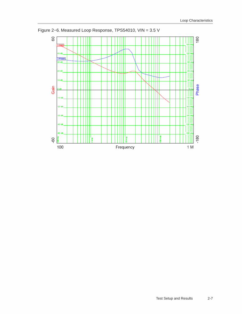
2.5 Loop Characteristics
The TPS54010EVM-067 loop response characteristics are shown inFigure 2−5 and Figure 2−6. Gain and phase plots are shown for each deviceat PVIN voltages of 2.2 V and 3.5 V.
Figure 2−5. Measured Loop Response, TPS54010, PVIN = 2.2 V
Loop Characteristics
2-7Test Setup and Results
Figure 2−6. Measured Loop Response, TPS54010, VIN = 3.5 V

Output Voltage Ripple
2-8
2.6 Output Voltage Ripple
The TPS54010EVM−067 output voltage ripple is shown in Figure 2−7. Theinput voltages are PVIN = 2.5 V and VIN = 3.3 V for the TPS54010. Outputcurrent is the rated full load of 14 A. Voltage is measured directly across outputcapacitors.
Figure 2−7. Measured Output Voltage Ripple, TPS54010
VO (AC) = 10 mV/div
Vphase = 1 mV/div
t − Time Scale 500 ns/div

Input Voltage Ripple
2-9Test Setup and Results
2.7 Input Voltage Ripple
The TPS54010EVM−067 output voltage ripple is shown in Figure 2−8. Theinput voltages PVIN = 2.5 V and VIN = 3.3 V for the TPS54010. Output currentfor each device is rated full load of 14 A.
Figure 2−8. Input Voltage Ripple, TPS54010
VI (RIPPLE) = 100 mV/div (ac Coupled)
V(PH) = 1 V/div
t − Time = 500 ns/div
2.8 Powering Up and Down
The TPS54010EVM-067 start-up waveforms are shown in Figure 2−9 andFigure 2−10. In Figure 2−9, the top trace shows VIN charging up from 0 V to3.3 V. When the input voltage reaches the internally set UVLO thresholdvoltage, the slow−start sequence begins. After a delay, Vo begins to ramp uplinearly at the externally set slow−start rate toward 1.5 V. In this case, the PVINvoltage rail is already present at VIN power up. In Figure 2−10, the outputvoltage is shown relative to SS/ENA. PVIN and VIN are applied to the EVMwhile SS/ENA is held low, disabling the device. When SS/ENA is released, theslow−start voltage begins to ramp up at the externally set rate. When theSS/ENA voltage reaches the enable threshold voltage of 1.2 V, the outputvoltage begins to ramp up toward its final value of 1.5 V.

Powering Up and Down
2-10
Figure 2−9. Power Up, VOUT Relative to VIN
VIN= 1 V/div
VOUT = 1 V/div
t − Time = 5 ms/div
Figure 2−10. Power Up, VOUT Relative to SS/ENA
V(SS/EBA)= 1 V/div
VOUT = 1 V/div
t − Time = 10 ms/div

3-1Board Layout
This chapter provides a description of the TPS54010EVM−067 board layoutand layer illustrations.
Topic Page
3.1 Layout 3-2. . . . . . . . . . . . . . . . . . . . . . . . . . . . . . . . . . . . . . . . . . . . . . . . . . . . . . .
Chapter 3

Layout
3-2
3.1 Layout
The board layout for the TPS54010EVM-067 is shown in Figure 3−1 throughNO TAG. The top−side layer of the TPS54010EVM-067 is laid out in a mannertypical of a user application. The top, bottom, and internal ground layers are2.0-oz. copper.
The top layer contains the main power traces for Vin, Vout, and Vphase. Alsoon the top layer are connections for the remaining pins of the TPS54010 anda large area filled with ground. The bottom layer contains ground and Voutcopper areas, and some signal routing. The two internal layers are dedicatedground layers. The top and bottom and internal ground traces are connectedwith multiple vias placed around the board including 10 directly under theTPS54010 device to provide a thermal path from the PowerPAD land toground.
The input decoupling capacitors (C1, C9, C10, and C11), bias decouplingcapacitor (C4), and bootstrap capacitor (C3) are all located as close to the ICas possible. In addition, the compensation components are also located closeto the IC. The compensation circuit ties to the output voltage at the point ofregulation, adjacent to the high-frequency bypass output capacitor.
Figure 3−1. Top−Side Layout

Layout
3-3Board Layout
Figure 3−2. Internal Ground Layer 2
Figure 3−3. Internal Ground Layer 3

3-4
Figure 3−4. Bottom−Side Layout (Looking From Top Side)
Figure 3−5. Top−SIde Assembly

4-1Schematic and Bill of Materials
This chapter presents the TPS54010EVM−067 schematic and bill ofmaterials.
Topic Page
4.1 Schematic 4-2. . . . . . . . . . . . . . . . . . . . . . . . . . . . . . . . . . . . . . . . . . . . . . . . . . . .
4.2 Bill of Materials 4-3. . . . . . . . . . . . . . . . . . . . . . . . . . . . . . . . . . . . . . . . . . . . . . .
Chapter 4

Schematic
4-2
4.1 Schematic
The schematic for the TPS54010EVM−067 is shown in Figure 4−1.
Figure 4−1. TPS54010EVM-067 Schematic

Bill of Materials
4-3Schematic and Bill of Materials
4.2 Bill of Materials
Table 4−1 contains the bill of materials for the TPS54010EVM−067.
Table 4−1.TPS54010EVM-067 Bill of Materials
Count RefDes Description Size MFR Part Number
1 C1 Capacitor, POSCAP, 330-µF, 6.3−V, 10 µW,20%
E Sanyo 6TPD330M
1 C13 Capacitor, ceramic, 0.1-µF, 16−V, X7R, 10% 603 std std
1 C2 Capacitor, ceramic, 100-µF 6.3−V, X5R, 20% 1210 TDK C3225X5R0J107M
− C12 Capacitor, ceramic, 100-µF, 6.3−V, X5R, 20% 1210 TDK C3225X5R0J107M
2 C3, C5 Capacitor, ceramic, 0.047-µF, 25−V, X7R,10%
603 std std
2 C4, C11 Capacitor, ceramic, 1.0-µF, 10−V, X5R, 10% 603 std std
2 C6, C14 Capacitor, ceramic, 3300-pF, 50−V, X7R, 10% 603 std std
1 C7 Capacitor, ceramic, 120-pF, 50−V, NPO, 10% 603 std std
1 C8 Capacitor, ceramic, 1500-pF, 50−V, X7R, 10% 603 std std
2 C9, C10 Capacitor, ceramic, 10-µF 16−V, X5R, 20% 1210 TDK C3225X5R1C106M
2 J1, J3 Terminal block, 2−pin, 15−A, 5,1 mm 148830 OST ED1609
1 J2 Terminal block, 2−pin, 6−A, 3,5 mm 75525 OST ED1514
1 J4 Header, 3−pin, 100 mil spacing, (36−pin strip) 0.100 x 3 Sullins PTC36SAAN
2 J5, JP1 Header, 2−pin, 100 mil spacing, (36−pin strip) 0.100 x 2 Sullins PTC36SAAN
3 — Shunt, 100−mil, black 0.1 3M 929950−00
1 L1 Inductor, SMT, 0.68-µH, 25A, 6 mΩ 0.270 sq Vishay IHLP−2525CZ−01
2 R1, R6 Resistor, chip, 10.0 kΩ, 1/16−W, 1% 603 Std Std
1 R2 Resistor, chip, 14.7 kΩ, 1/16−W, 1% 603 Std Std
1 R3 Resistor, chip, 4.64 kΩ,, 1/16−W, 1% 603 Std Std
1 R4 Resistor, chip, 71.5 kΩ, 1/16−W, 1% 603 Std Std
1 R5 Resistor, chip, 422 Ω,, 1/16−W, 1% 603 std std
1 R7 Resistor, chip, 0−Ω, 1/16−W, 1% 603 Std Std
1 R8 Resistor, chip, 2.4−Ω, 1/8−W, 1% 1206 std std
6 TP1, TP2,TP4, TP5,TP6, TP7
Test point, red, 1 mm 0.038”, 6400” Farnell 240−345
2 TP3, TP8 Test point, black, 1 mm 0.038”, 6400” Farnell 240−333
1 U1 IC, IFET power controller, 2.2 to 4−V, 14−A PWP28 TI TPS54010PWP
1 — PCB, 3 In x 3 In x 0.062 In Any HPA067

4-4

![OFDM error floor based EVM estimation Error Floor Based EVM Estimation.pdfAWGN source producing the same BER (and EVM) degradation. [1]: The resulting EVM(BER) curves were verified](https://img.pdfslide.us/doc/110x75/5f2e7bc463c3260b31328bb2/ofdm-error-floor-based-evm-estimation-error-floor-based-evm-awgn-source-producing.jpg)

![CSEPEl PANNONIA IS]shveiprom.com/cats/SCHMETZ/CHZEPEL-PANNONIA-DURKOPP...DORKOPP ADLER £51 030-10 ALL CLASSES EXCEPT 067 TO 69 067 62 S 067-262 Z 067 272 NH 1 067-372 TO 373 067-1000](https://img.pdfslide.us/doc/110x75/60aa411c98eb557f2754c8e9/csepel-pannonia-is-dorkopp-adler-51-030-10-all-classes-except-067-to-69-067.jpg)