Embed Size (px)
Citation preview
28m:
VIN OUT
EN/UVLO
dV/dT
GND
BFET
TPS25924x
ILIM
RLIM
COUT
CdVdT
R1
R2
VIN OUT
Product
Folder
Sample &Buy
Technical
Documents
Tools &
Software
Support &Community
An IMPORTANT NOTICE at the end of this data sheet addresses availability, warranty, changes, use in safety-critical applications,intellectual property matters and other important disclaimers. PRODUCTION DATA.
TPS259240, TPS259241SLVSCU9B –AUGUST 2015–REVISED SEPTEMBER 2016
TPS25924x 12-V eFuse with Over Voltage Protection and Blocking FET Control
1
1 Features1• VOPERATING = 4.5 V to 13.8 V, VABSMAX = 20 V• Integrated 28-mΩ Pass MOSFET• Fixed 15-V Over Voltage Clamp• 1-A to 5-A Adjustable ILIMIT
• ±8% ILIMIT Accuracy at 3.7 A• Reverse Current Blocking Support• Programmable OUT Slew Rate, UVLO• Built-in Thermal Shutdown• UL 2367 Recognized – File No. E339631*
– *RILIM ≤ 130 kΩ (5 A maximum)• Safe During Single Point Failure Test (UL60950)• Small Foot Print – 10L (3 mm x 3 mm) VSON
2 Applications• Adapter Powered Devices• HDD and SSD Drives• Set Top Boxes• Servers / AUX Supplies• Fan Control• PCI/PCIe Cards
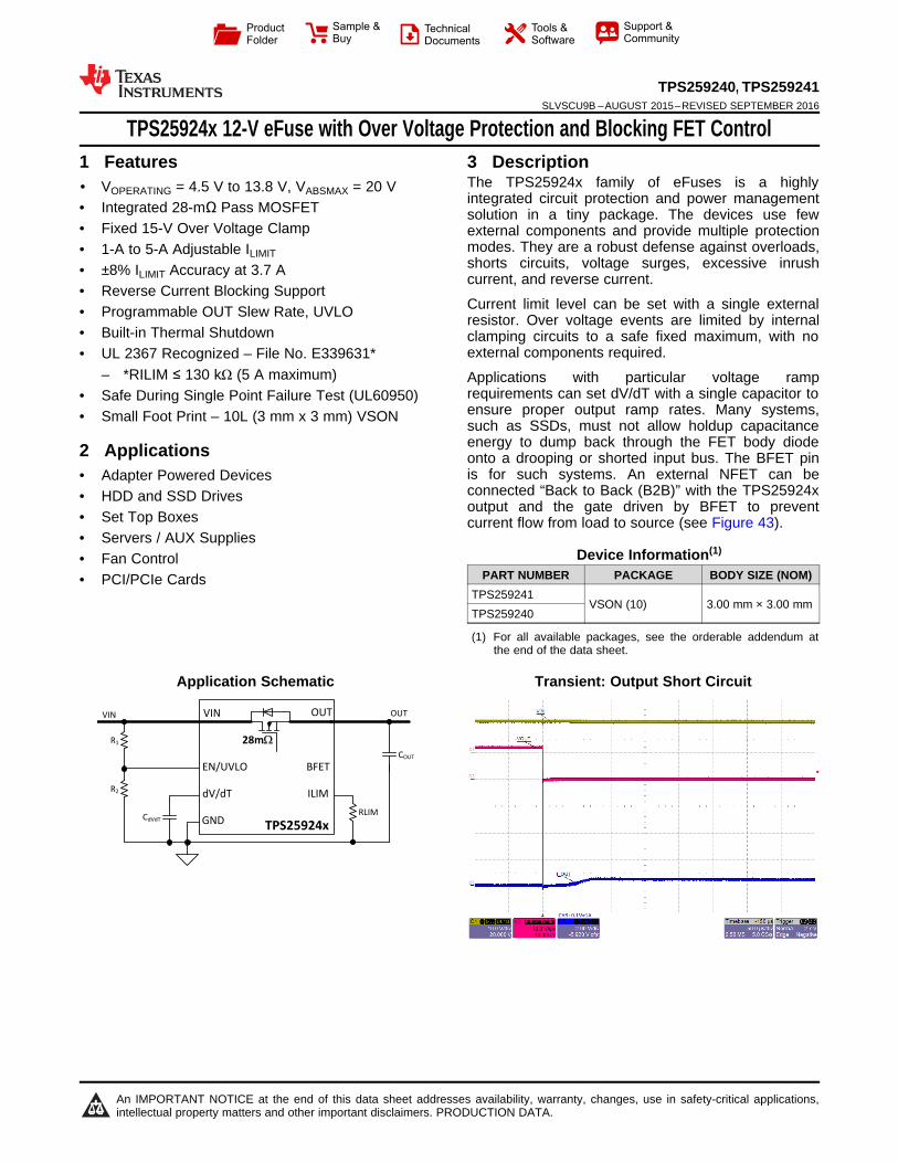
3 DescriptionThe TPS25924x family of eFuses is a highlyintegrated circuit protection and power managementsolution in a tiny package. The devices use fewexternal components and provide multiple protectionmodes. They are a robust defense against overloads,shorts circuits, voltage surges, excessive inrushcurrent, and reverse current.
Current limit level can be set with a single externalresistor. Over voltage events are limited by internalclamping circuits to a safe fixed maximum, with noexternal components required.
Applications with particular voltage ramprequirements can set dV/dT with a single capacitor toensure proper output ramp rates. Many systems,such as SSDs, must not allow holdup capacitanceenergy to dump back through the FET body diodeonto a drooping or shorted input bus. The BFET pinis for such systems. An external NFET can beconnected “Back to Back (B2B)” with the TPS25924xoutput and the gate driven by BFET to preventcurrent flow from load to source (see Figure 43).
Device Information(1)
PART NUMBER PACKAGE BODY SIZE (NOM)TPS259241
VSON (10) 3.00 mm × 3.00 mmTPS259240
(1) For all available packages, see the orderable addendum atthe end of the data sheet.
Application Schematic Transient: Output Short Circuit
2
TPS259240, TPS259241SLVSCU9B –AUGUST 2015–REVISED SEPTEMBER 2016 www.ti.com
Product Folder Links: TPS259240 TPS259241
Submit Documentation Feedback Copyright © 2015–2016, Texas Instruments Incorporated
Table of Contents1 Features .................................................................. 12 Applications ........................................................... 13 Description ............................................................. 14 Revision History..................................................... 25 Device Comparison Table ..................................... 36 Pin Configuration and Functions ......................... 37 Specifications......................................................... 4
7.1 Absolute Maximum Ratings ..................................... 47.2 ESD Ratings ............................................................ 47.3 Recommended Operating Conditions...................... 47.4 Thermal Information .................................................. 57.5 Electrical Characteristics.......................................... 57.6 Timing Requirements ............................................... 67.7 Typical Characteristics .............................................. 7
8 Detailed Description ............................................ 138.1 Overview ................................................................. 138.2 Functional Block Diagram ....................................... 138.3 Feature Description................................................. 138.4 Device Functional Modes........................................ 16
9 Application and Implementation ........................ 179.1 Application Information............................................ 179.2 Typical Applications ............................................... 17
10 Power Supply Recommendations ..................... 2310.1 Transient Protection .............................................. 2310.2 Output Short-Circuit Measurements ..................... 24
11 Layout................................................................... 2511.1 Layout Guidelines ................................................. 2511.2 Layout Example .................................................... 25
12 Device and Documentation Support ................. 2612.1 Device Support .................................................... 2612.2 Documentation Support ....................................... 2612.3 Related Links ........................................................ 2612.4 Receiving Notification of Documentation Updates 2612.5 Community Resources.......................................... 2612.6 Trademarks ........................................................... 2612.7 Electrostatic Discharge Caution............................ 2612.8 Glossary ................................................................ 27
13 Mechanical, Packaging, and OrderableInformation ........................................................... 27
4 Revision History
Changes from Revision A (August 2015) to Revision B Page
• Added section: Controlled Power Down using TPS25924x ................................................................................................. 22
Changes from Original (August 2015) to Revision A Page
• Changed from Product Preview to Production Data .............................................................................................................. 1
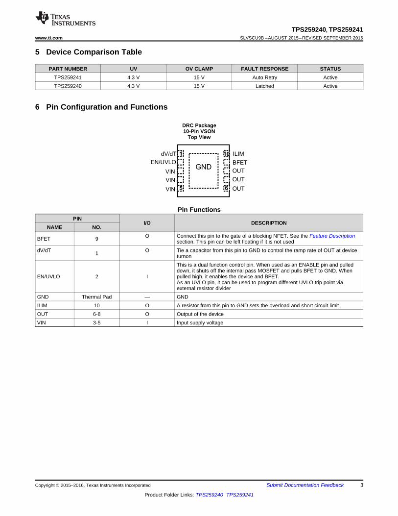
GND
dV/dT
VIN
EN/UVLO
ILIM
BFET
OUT
OUT
OUT
VIN
VIN
1
5 6
10
3
TPS259240, TPS259241www.ti.com SLVSCU9B –AUGUST 2015–REVISED SEPTEMBER 2016
Product Folder Links: TPS259240 TPS259241
Submit Documentation FeedbackCopyright © 2015–2016, Texas Instruments Incorporated
5 Device Comparison Table
PART NUMBER UV OV CLAMP FAULT RESPONSE STATUSTPS259241 4.3 V 15 V Auto Retry ActiveTPS259240 4.3 V 15 V Latched Active
6 Pin Configuration and Functions
DRC Package10-Pin VSON
Top View
Pin FunctionsPIN
I/O DESCRIPTIONNAME NO.
BFET 9 O Connect this pin to the gate of a blocking NFET. See the Feature Descriptionsection. This pin can be left floating if it is not used
dV/dT 1 O Tie a capacitor from this pin to GND to control the ramp rate of OUT at deviceturnon
EN/UVLO 2 I
This is a dual function control pin. When used as an ENABLE pin and pulleddown, it shuts off the internal pass MOSFET and pulls BFET to GND. Whenpulled high, it enables the device and BFET.As an UVLO pin, it can be used to program different UVLO trip point viaexternal resistor divider
GND Thermal Pad — GNDILIM 10 O A resistor from this pin to GND sets the overload and short circuit limitOUT 6-8 O Output of the deviceVIN 3-5 I Input supply voltage
4
TPS259240, TPS259241SLVSCU9B –AUGUST 2015–REVISED SEPTEMBER 2016 www.ti.com
Product Folder Links: TPS259240 TPS259241
Submit Documentation Feedback Copyright © 2015–2016, Texas Instruments Incorporated
(1) Stresses beyond those listed under Absolute Maximum Ratings may cause permanent damage to the device. These are stress ratingsonly, which do not imply functional operation of the device at these or any other conditions beyond those indicated under RecommendedOperating Conditions. Exposure to absolute-maximum-rated conditions for extended periods may affect device reliability.
(2) All voltage values, except differential voltages, are with respect to network ground terminal.
7 Specifications
7.1 Absolute Maximum Ratingsover operating temperature range (unless otherwise noted) (1) (2)
MIN MAX UNITVIN
Supply voltage (1) –0.3 20V
VIN (10-ms transient) 22OUT
Output voltage–0.3 VIN + 0.3 V
OUT (transient < 1 µs) –1.2 VILIM
Voltage
–0.3 7
VEN/UVLO –0.3 7dV/dT –0.3 7BFET –0.3 30Tstg Storage temperature –65 150 °C
(1) JEDEC document JEP155 states that 500-V HBM allows safe manufacturing with a standard ESD control process.(2) JEDEC document JEP157 states that 250-V CDM allows safe manufacturing with a standard ESD control process.
7.2 ESD RatingsVALUE UNIT
V(ESD) Electrostatic dischargeHuman body model (HBM), per ANSI/ESDA/JEDEC JS-001 (1) ±2000
VCharged device model (CDM), per JEDEC specification JESD22-C101 (2) ±500
7.3 Recommended Operating Conditionsover operating free-air temperature range (unless otherwise noted)
MIN TYP MAX UNITVIN
Input voltage
4.5 12 13.8
VBFET 0 VIN+6dV/dT, EN/UVLO 0 6ILIM 0 3IOUT Continuous output current 0 5 AILIM Resistance 10 100 162 kΩOUT
External capacitance0.1 1 1000 µF
dV/dT 1 1000 nFTJ Operating junction temperature –40 25 125 °CTA Operating Ambient temperature –40 25 85 °C
5
TPS259240, TPS259241www.ti.com SLVSCU9B –AUGUST 2015–REVISED SEPTEMBER 2016
Product Folder Links: TPS259240 TPS259241
Submit Documentation FeedbackCopyright © 2015–2016, Texas Instruments Incorporated
(1) For more information about traditional and new thermal metrics, see the Semiconductor and IC Package Thermal Metrics applicationreport.
7.4 Thermal Informationover operating free-air temperature range (unless otherwise noted) (1)
THERMAL METRICTPS25924x
UNITDRC (VSON)10 PINS
RθJA Junction-to-ambient thermal resistance 45.9 °C/WRθJCtop Junction-to-case (top) thermal resistance 53 °C/WRθJB Junction-to-board thermal resistance 21.2 °C/WψJT Junction-to-top characterization parameter 1.2 °C/WψJB Junction-to-board characterization parameter 21.4 °C/WRθJCbot Junction-to-case (bottom) thermal resistance 5.9 °C/W
(1) These parameters are provided for reference only and do not constitute part of TI's published device specifications for purposes of TI'sproduct warranty.
(2) Pulsed testing techniques used during this test maintain junction temperature approximately equal to ambient temperature.
7.5 Electrical Characteristics–40°C ≤ TJ ≤ +125°C, VIN = 12 V, VEN /UVLO = 2 V, RILIM = 100 kΩ, CdVdT = OPEN. All voltages referenced to GND (unlessotherwise noted).
PARAMETER TEST CONDITIONS MIN TYP MAX UNIT
VIN (INPUT SUPPLY)
VUVR UVLO threshold, rising 4.15 4.3 4.45 V
VUVhyst UVLO hysteresis (1) 5%
IQONSupply current
Enabled: EN/UVLO = 2 V 0.3 0.42 0.55 mA
IQOFF EN/UVLO = 0 V 0.13 0.225 mA
VOVC Over-voltage clamp VIN > 16.5 V, IOUT = 10 mA 13.8 15 16.5 V
EN/UVLO (ENABLE/UVLO INPUT)
VENR EN threshold voltage, rising 1.37 1.4 1.44 V
VENF EN threshold voltage, falling 1.32 1.35 1.39 V
IEN EN Input leakage current 0 V ≤ VEN ≤ 5 V –100 0 100 nA
dV/dT (OUTPUT RAMP CONTROL)
IdVdT dV/dT charging current (1) VdVdT = 0 V 220 nA
RdVdT_disch dV/dT discharging resistance EN/UVLO = 0 V, IdVdT = 10 mA sinking 50 73 100 Ω
VdVdTmax dV/dT max capacitor voltage (1) 5.5 V
GAINdVdT dV/dT to OUT gain (1) ΔVdVdT 4.85 V/V
ILIM (CURRENT LIMIT PROGRAMMING)
IILIM ILIM bias current (1) 10 µA
IOL
Overload current limit (2)
RILIM = 10 kΩ, VVIN-OUT = 1 V 1.02
ARILIM = 45.3 kΩ, VVIN-OUT = 1 V 1.79 2.10 2.42
RILIM = 100 kΩ, VVIN-OUT = 1 V 3.46 3.75 4.03
RILIM = 150 kΩ, VVIN-OUT = 1 V 4.5 5.1 5.7
IOL-R-ShortRILIM = 0 Ω, shorted resistor current limit (single point failuretest: UL60950) (1) 0.84 A
IOL-R-OpenRILIM = OPEN, open resistor current limit (single point failuretest: UL60950) (1) 0.73 A
ISCL Short-circuit current limit (2)
RILIM = 10 kΩ, VVIN-OUT = 12 V 1
ARILIM = 45.3 kΩ, VVIN-OUT = 12 V 1.66 1.98 2.37
RILIM = 100 kΩ, VVIN-OUT = 12 V 2.90 3.32 3.85
RILIM = 150 kΩ, VVIN-OUT = 12 V 3.7 4.5 5.5
RATIOFASTRIPFast-trip comparator level w.r.t.overload current limit (1) IFASTRIP : IOL 160%
VOpenILIMILIM open resistor detectthreshold (1) VILIM rising, RILIM = OPEN 3.1 V
6
TPS259240, TPS259241SLVSCU9B –AUGUST 2015–REVISED SEPTEMBER 2016 www.ti.com
Product Folder Links: TPS259240 TPS259241
Submit Documentation Feedback Copyright © 2015–2016, Texas Instruments Incorporated
Electrical Characteristics (continued)–40°C ≤ TJ ≤ +125°C, VIN = 12 V, VEN /UVLO = 2 V, RILIM = 100 kΩ, CdVdT = OPEN. All voltages referenced to GND (unlessotherwise noted).
PARAMETER TEST CONDITIONS MIN TYP MAX UNIT
OUT (PASS FET OUTPUT)
RDS(on) FET ON resistanceTJ = 25°C 21 28 37
mΩTJ = 125°C 39 48
IOUT-OFF-LKGOUT bias current in off state
VEN/UVLO = 0 V, VOUT = 0 V (sourcing) –5 0 1.2µA
IOUT-OFF-SINK VEN/UVLO = 0 V, VOUT = 300 mV (sinking) 10 15 20
BFET (BLOCKING FET GATE DRIVER)
IBFET BFET charging current (1) VBFET = VOUT 2 µA
VBFETmax BFET clamp voltage (1) VVIN +6.4 V
RBFETdischBFET discharging resistance toGND VEN/UVLO = 0 V, IBFET = 100 mA 15 26 36 Ω
TSD (THERMAL SHUT DOWN)
TSHDN TSD threshold, rising (1) 150 °C
TSHDNhyst TSD hysteresis (1) 10 °C
Thermal fault: latched or auto-retryTPS259240 Latched
TPS259241 Auto-retry
(1) These parameters are provided for reference only and do not constitute part of TI's published device specifications for purposes of TI'sproduct warranty.
7.6 Timing RequirementsPARAMETER TEST CONDITIONS MIN TYP MAX UNIT
TON Turnon delay (1) EN/UVLO → H to IVIN = 100 mA, 1-A resistive loadat OUT 220 µs
tOFFdly Turnoff delay (1) EN/UVLO↓ to BFET↓, CBFET = 0 0.4 µsdV/dT (OUTPUT RAMP CONTROL)
tdVdT Output ramp timeEN/UVLO → H to OUT = 11.7 V, CdVdT = 0 0.7 1 1.3
msEN/UVLO → H to OUT = 11.7 V, CdVdT = 1 nF (1) 12
ILIM (CURRENT LIMIT PROGRAMMING)tFastOffDly Fast-Trip comparator delay (1) IOUT > IFASTRIP to IOUT= 0 (Switch off) 300 nsBFET (BLOCKING FET GATE DRIVER)
tBFET-ON BFET Turnon duration (1) EN/UVLO → H to VBFET = 12 V, CBFET = 1 nF 4.2ms
EN/UVLO → H to VBFET = 12 V, CBFET = 10 nF 42
tBFET-OFF BFET Turnoff duration (1) EN/UVLO → L to VBFET = 1 V, CBFET = 1 nF 0.4µs
EN/UVLO → L to VBFET = 1 V, CBFET = 10 nF 1.4THERMAL SHUTDOWN (TSD)
tTSDdlyRetry delay after TSD recovery,TJ < [TSHDN - 10°C] (1) TPS259241 only 100 µs
20
25
30
35
40
45
-50 0 50 100 150
RD
SO
N (
m:
)
Temperature (oC)
150
170
190
210
230
250
-50 0 50 100 150
TO
N (P
s)
Temperature (oC)
0
0.1
0.2
0.3
0.4
0.5
0.6
0 5 10 15 20
I VIN
-ON (
mA
)
VIN (V)
125 °C85 °C25 °C-40 °C
C003
14.5
15
15.5
16
-50 0 50 100 150
VO
VC (
V)
Temperature (C)
10 mA
100 mA
500 mA
C005
4
4.05
4.1
4.15
4.2
4.25
4.3
4.35
-50 0 50 100 150
Inpu
t U
VLO
(R
isin
g, F
allin
g) (
V)
Temperature (C) C001
0
0.05
0.1
0.15
0.2
0.25
0 5 10 15 20
I Q-O
FF (
mA
)
VIN (V)
125 C 85 C 25 C -40 C
C002
7
TPS259240, TPS259241www.ti.com SLVSCU9B –AUGUST 2015–REVISED SEPTEMBER 2016
Product Folder Links: TPS259240 TPS259241
Submit Documentation FeedbackCopyright © 2015–2016, Texas Instruments Incorporated
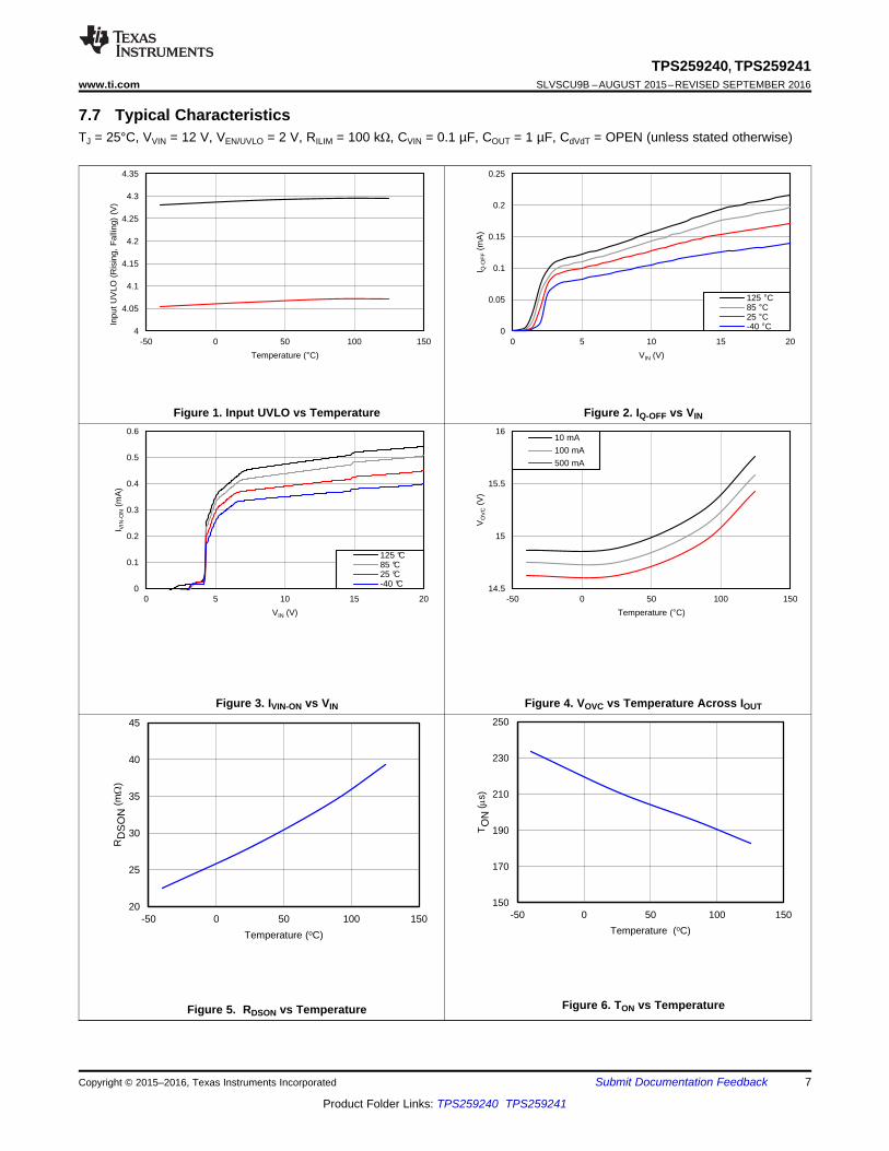
7.7 Typical CharacteristicsTJ = 25°C, VVIN = 12 V, VEN/UVLO = 2 V, RILIM = 100 kΩ, CVIN = 0.1 µF, COUT = 1 µF, CdVdT = OPEN (unless stated otherwise)
Figure 1. Input UVLO vs Temperature Figure 2. IQ-OFF vs VIN
Figure 3. IVIN-ON vs VIN Figure 4. VOVC vs Temperature Across IOUT
Figure 5. RDSON vs Temperature Figure 6. TON vs Temperature
Temperature (oC)
I OL-
R-S
HO
RT (
A)
-50 0 50 100 1500.75
0.8
0.85
0.9
0.95
D001Temperature (oC)
I OL-
R-O
PE
N (
A)
-50 0 50 100 1500.65
0.7
0.75
0.8
D001
VEN (V)
I EN (
nA)
0 1 2 3 4 50.1
1
10
100
D016
125qC85qC25qC-40qC
1.34
1.35
1.36
1.37
1.38
1.39
1.4
1.41
-50 0 50 100 150
VE
N-V
IHV
EN
-VIL
(V)
Temperature (oC)
Rising
Falling
205
210
215
220
225
230
-50 0 50 100 150
I dV
dT (
nA)
Temperature (C) C010
0
50
100
150
0 2 4 6 8 10
TdV
dT (
ms)
CdVdT (nF)
125 C 85 C 25 C -40 C
C013
8
TPS259240, TPS259241SLVSCU9B –AUGUST 2015–REVISED SEPTEMBER 2016 www.ti.com
Product Folder Links: TPS259240 TPS259241
Submit Documentation Feedback Copyright © 2015–2016, Texas Instruments Incorporated
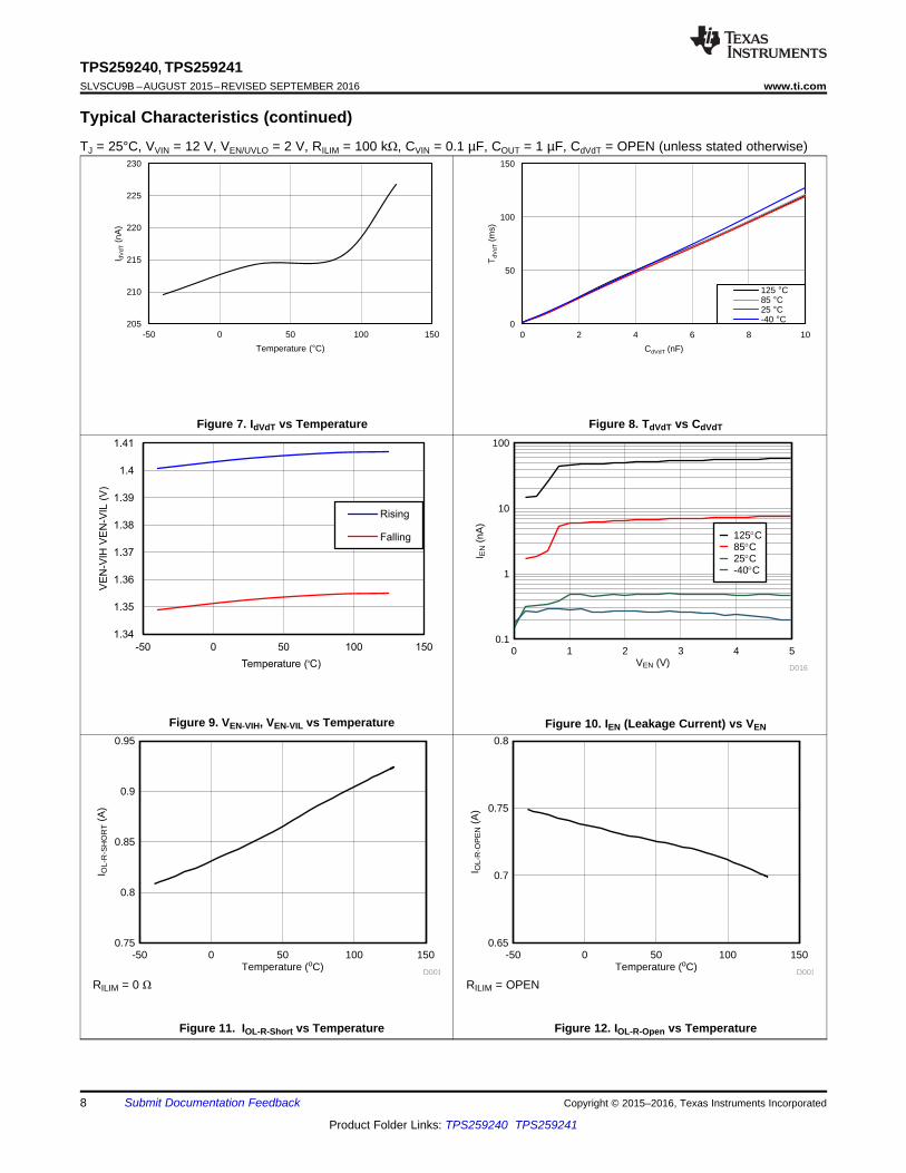
Typical Characteristics (continued)TJ = 25°C, VVIN = 12 V, VEN/UVLO = 2 V, RILIM = 100 kΩ, CVIN = 0.1 µF, COUT = 1 µF, CdVdT = OPEN (unless stated otherwise)
Figure 7. IdVdT vs Temperature Figure 8. TdVdT vs CdVdT
Figure 9. VEN-VIH, VEN-VIL vs Temperature Figure 10. IEN (Leakage Current) vs VEN
RILIM = 0 Ω
Figure 11. IOL-R-Short vs Temperature
RILIM = OPEN
Figure 12. IOL-R-Open vs Temperature
-6
-5
-4
-3
-2
-1
0
1
-50 0 50 100 150
I OL
,I S
C(%
Norm
aliz
ed)
Temperature (oC)
IOL-45.3k
ISC-45.3k
-12
-10
-8
-6
-4
-2
0
2
-50 0 50 100 150
I OL
,I S
C(%
No
rma
lized
)
Temperature (oC)
IOL-100k
ISC-100k
VVIN-OUT (V)
I VO
UT (
A)
0 0.5 1 1.5 21
2
3
4
5
6
D027
125qC85qC25qC-40qC
-16
-14
-12
-10
-8
-6
-4
-2
0
2
-50 0 50 100 150
I OL
,I S
C(%
No
rma
lized
)
Temperature (oC)
IOL-150k
ISC-150k
VVIN-OUT (V)
I VO
UT (
A)
0 0.5 1 1.5 21
1.5
2
2.5
3
3.5
4
D028
125qC85qC25qC-40qC
VVIN-OUT (V)
I VO
UT (
A)
0 0.5 1 1.5 21
1.2
1.4
1.6
1.8
2
2.2
D029
125qC85qC25qC-40qC
9
TPS259240, TPS259241www.ti.com SLVSCU9B –AUGUST 2015–REVISED SEPTEMBER 2016
Product Folder Links: TPS259240 TPS259241
Submit Documentation FeedbackCopyright © 2015–2016, Texas Instruments Incorporated
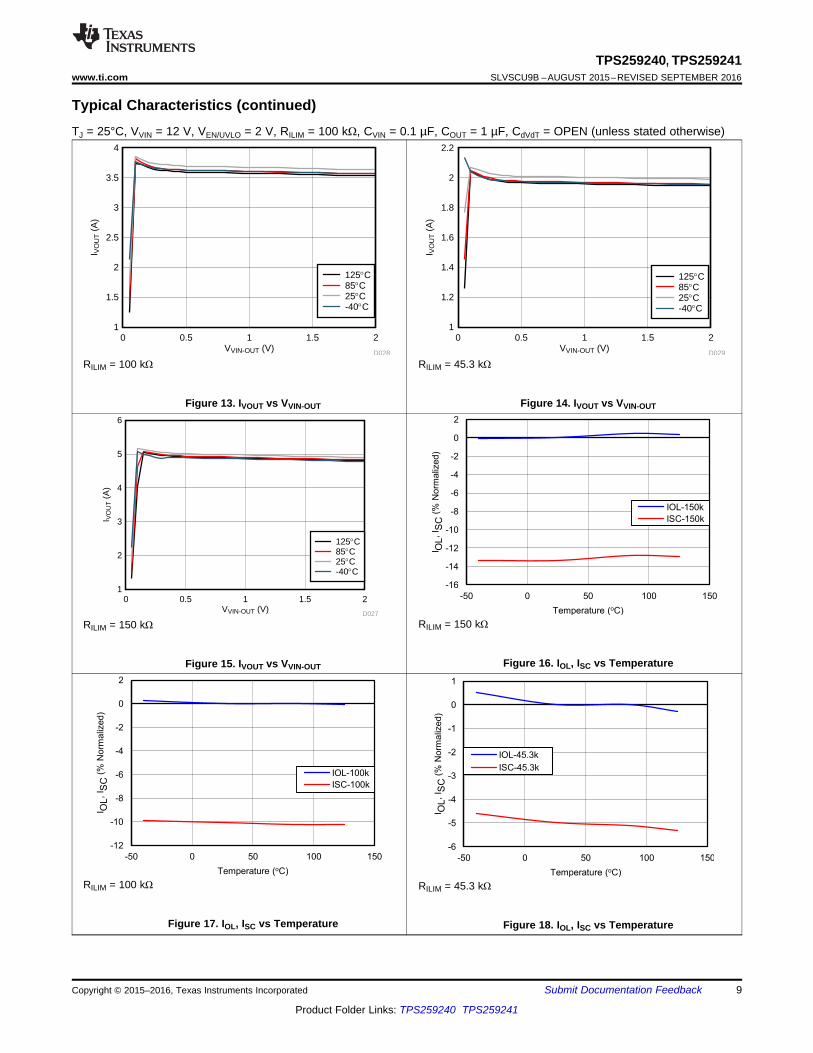
Typical Characteristics (continued)TJ = 25°C, VVIN = 12 V, VEN/UVLO = 2 V, RILIM = 100 kΩ, CVIN = 0.1 µF, COUT = 1 µF, CdVdT = OPEN (unless stated otherwise)
RILIM = 100 kΩ
Figure 13. IVOUT vs VVIN-OUT
RILIM = 45.3 kΩ
Figure 14. IVOUT vs VVIN-OUT
RILIM = 150 kΩ
Figure 15. IVOUT vs VVIN-OUT
RILIM = 150 kΩ
Figure 16. IOL, ISC vs Temperature
RILIM = 100 kΩ
Figure 17. IOL, ISC vs Temperature
RILIM = 45.3 kΩ
Figure 18. IOL, ISC vs Temperature
VIN
VOUT
C2C2
C3
VIN
VOUT
C2C2
C3
EN
I_IN
C2C1
C4
RILIM Resistor (k:)
Ove
rload
Cur
rent
Lim
it (A
)
0 20 40 60 80 100 1200
0.5
1
1.5
2
2.5
3
3.5
4
D001Power Dissipation (W)
The
rmal
Shu
tdow
n T
ime
(ms)
0.1 1 10 1000.1
1
10
100
1000
10000
D001
TA = -40oCTA = 25oCTA = 85oCTA = 125oC
Overload Current Limit (A)
Acc
urac
y (P
roce
ss, V
olta
ge, T
empe
ratu
re)
(%)
1 1.5 2 2.5 3 3.5 4 4.5 5 5.50
5
10
15
20
25
30
35
D001
3.05
3.06
3.07
3.08
3.09
3.1
-50 0 50 100 150
ILIM
Ope
n D
etec
t Thr
esho
ld (
V)
Temperature (oC)
10
TPS259240, TPS259241SLVSCU9B –AUGUST 2015–REVISED SEPTEMBER 2016 www.ti.com
Product Folder Links: TPS259240 TPS259241
Submit Documentation Feedback Copyright © 2015–2016, Texas Instruments Incorporated
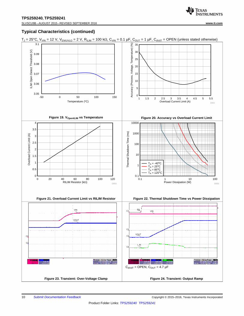
Typical Characteristics (continued)TJ = 25°C, VVIN = 12 V, VEN/UVLO = 2 V, RILIM = 100 kΩ, CVIN = 0.1 µF, COUT = 1 µF, CdVdT = OPEN (unless stated otherwise)
Figure 19. VOpenILIM vs Temperature Figure 20. Accuracy vs Overload Current Limit
Figure 21. Overload Current Limit vs RILIM Resistor Figure 22. Thermal Shutdown Time vs Power Dissipation
Figure 23. Transient: Over-Voltage Clamp
CdVdT = OPEN, COUT = 4.7 µF
Figure 24. Transient: Output Ramp
VOUT
C3
I_IN
C2C1
C2
VIN
EN
C4
VOUTC3
I_IN
C2C1
C2
VIN
EN
C4
VOUT
C3
BFET
C2C1
C2
EN
VOUT
C3
BFET
C2C1
C2
VIN
VIN
VOUT
I-IN
EN
C2
C4
C3
C1
VOUT
C3I_OUT
C2C1
C4
EN
11
TPS259240, TPS259241www.ti.com SLVSCU9B –AUGUST 2015–REVISED SEPTEMBER 2016
Product Folder Links: TPS259240 TPS259241
Submit Documentation FeedbackCopyright © 2015–2016, Texas Instruments Incorporated
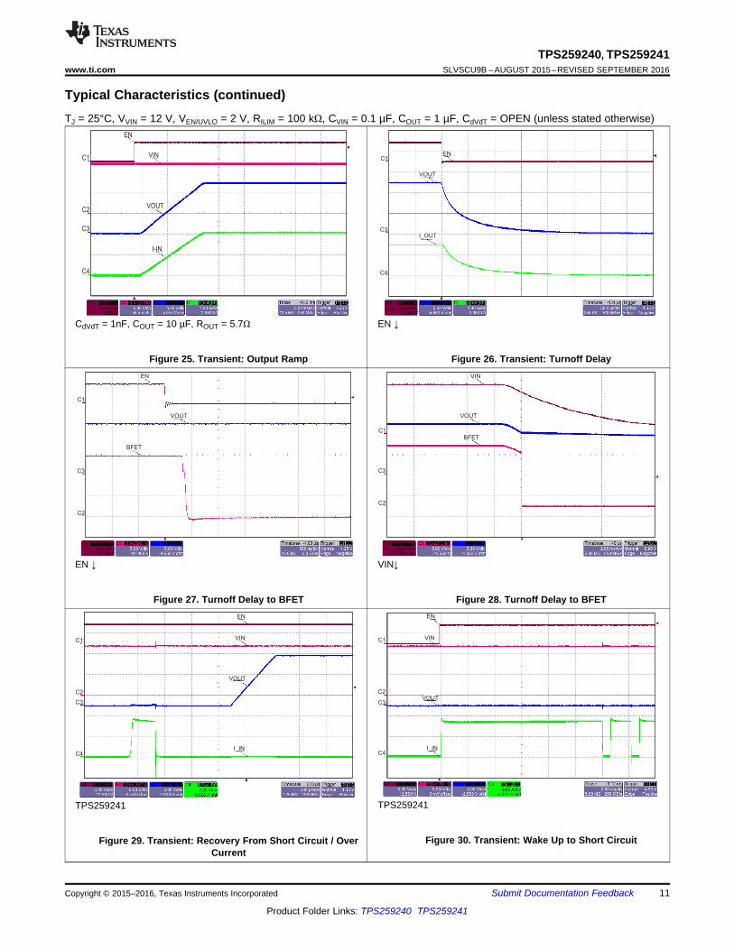
Typical Characteristics (continued)TJ = 25°C, VVIN = 12 V, VEN/UVLO = 2 V, RILIM = 100 kΩ, CVIN = 0.1 µF, COUT = 1 µF, CdVdT = OPEN (unless stated otherwise)
CdVdT = 1nF, COUT = 10 µF, ROUT = 5.7Ω
Figure 25. Transient: Output Ramp
EN ↓
Figure 26. Transient: Turnoff Delay
EN ↓
Figure 27. Turnoff Delay to BFET
VIN↓
Figure 28. Turnoff Delay to BFET
TPS259241
Figure 29. Transient: Recovery From Short Circuit / OverCurrent
TPS259241
Figure 30. Transient: Wake Up to Short Circuit
VOUT
C3
I_IN
C2C1
C2
VIN
EN
C4
12
TPS259240, TPS259241SLVSCU9B –AUGUST 2015–REVISED SEPTEMBER 2016 www.ti.com
Product Folder Links: TPS259240 TPS259241
Submit Documentation Feedback Copyright © 2015–2016, Texas Instruments Incorporated
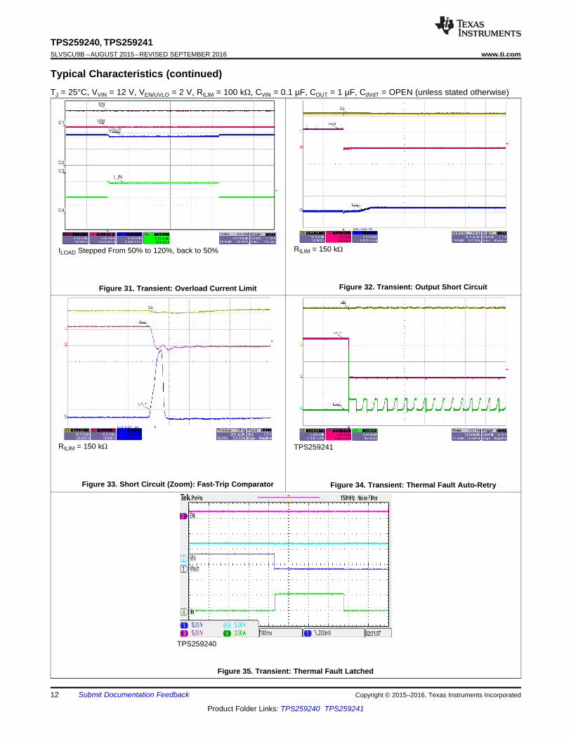
Typical Characteristics (continued)TJ = 25°C, VVIN = 12 V, VEN/UVLO = 2 V, RILIM = 100 kΩ, CVIN = 0.1 µF, COUT = 1 µF, CdVdT = OPEN (unless stated otherwise)
ILOAD Stepped From 50% to 120%, back to 50%
Figure 31. Transient: Overload Current Limit
RILIM = 150 kΩ
Figure 32. Transient: Output Short Circuit
RILIM = 150 kΩ
Figure 33. Short Circuit (Zoom): Fast-Trip Comparator
TPS259241
Figure 34. Transient: Thermal Fault Auto-Retry
TPS259240
Figure 35. Transient: Thermal Fault Latched
3,
4,
5
VIN
2
EN/
UVLO +1.4V
1.35V
4.3V
4.08V
+ UVLO
EN
TSD
220nA
70pF
6V
SWEN
4.8x
80W
10
ILIM
+
VIN
+
+
ILIMIT
1.6*ILIMIT
10 Am
6V
GATE
CONTROL
Charge
Pump
Over
Voltage
Thermal
Shutdown
6,
7,
8
28mW
BFET
9
SWEN
22W
2 Am
SWEN
Current
Sense
1
dV/dT
EP
GND
OUT
Fast Trip
Comp
13
TPS259240, TPS259241www.ti.com SLVSCU9B –AUGUST 2015–REVISED SEPTEMBER 2016
Product Folder Links: TPS259240 TPS259241
Submit Documentation FeedbackCopyright © 2015–2016, Texas Instruments Incorporated
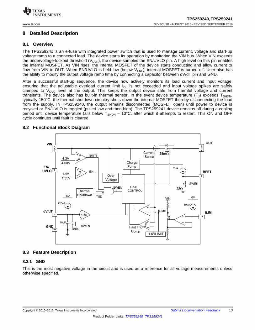
8 Detailed Description
8.1 OverviewThe TPS25924x is an e-fuse with integrated power switch that is used to manage current, voltage and start-upvoltage ramp to a connected load. The device starts its operation by monitoring the VIN bus. When VIN exceedsthe undervoltage-lockout threshold (VUVR), the device samples the EN/UVLO pin. A high level on this pin enablesthe internal MOSFET. As VIN rises, the internal MOSFET of the device starts conducting and allow current toflow from VIN to OUT. When EN/UVLO is held low (below VENF), internal MOSFET is turned off. User also hasthe ability to modify the output voltage ramp time by connecting a capacitor between dV/dT pin and GND.
After a successful start-up sequence, the device now actively monitors its load current and input voltage,ensuring that the adjustable overload current limit IOL is not exceeded and input voltage spikes are safelyclamped to VOVC level at the output. This keeps the output device safe from harmful voltage and currenttransients. The device also has built-in thermal sensor. In the event device temperature (TJ) exceeds TSHDN,typically 150°C, the thermal shutdown circuitry shuts down the internal MOSFET thereby disconnecting the loadfrom the supply. In TPS259240, the output remains disconnected (MOSFET open) until power to device isrecycled or EN/UVLO is toggled (pulled low and then high). The TPS259241 device remains off during a coolingperiod until device temperature falls below TSHDN – 10°C, after which it attempts to restart. This ON and OFFcycle continues until fault is cleared.
8.2 Functional Block Diagram
8.3 Feature Description
8.3.1 GNDThis is the most negative voltage in the circuit and is used as a reference for all voltage measurements unlessotherwise specified.
( )6dVdT IN dVdTT = 10 V C 70 pF´ ´ +
OUTdVDesired output slew rate
dT=
OUT dVdT dVdT
dVdT INT
dV I GAIN
dt C C=
+
´
14
TPS259240, TPS259241SLVSCU9B –AUGUST 2015–REVISED SEPTEMBER 2016 www.ti.com
Product Folder Links: TPS259240 TPS259241
Submit Documentation Feedback Copyright © 2015–2016, Texas Instruments Incorporated
Feature Description (continued)8.3.2 VINInput voltage to the TPS25924x. A ceramic bypass capacitor close to the device from VIN to GND isrecommended to alleviate bus transients. The recommended operating voltage range is 4.5 V to 13.8 V forTPS25924x. The device can continuously sustain a voltage of 20 V on VIN pin. However, above therecommended maximum bus voltage, the device will be in over-voltage protection (OVP) mode, limiting theoutput voltage to VOVC. The power dissipation in OVP mode is PD_OVP = (VVIN – VOVC) x IOUT, which canpotentially heat up the device and cause thermal shutdown.
8.3.3 dV/dTConnect a capacitor from this pin to GND to control the slew rate of the output voltage at power-on. This pin canbe left floating to obtain a predetermined slew rate (minimum TdVdT) on the output. Equation governing slew rateat start-up is shown in Equation 1:
where• IdVdT = 220 nA (Typical)• CINT = 70 pF (Typical)• GAINdVdT = 4.85
(1)
The total ramp time (TdVdT) for 0 to VIN can be calculated using Equation 2:
(2)
For details on how to select an appropriate charging time/rate, refer to the applications section Setting OutputVoltage Ramp Time (TdVdT).
8.3.4 BFETConnect this pin to an external NFET that can be used to disconnect input supply from rest of the system in theevent of power failure at VIN. The BFET pin is controlled by either input UVLO (VUVR) event or EN/UVLO (seeTable 1). BFET can source charging current of 2 µA (TYP) and sink (discharge) current from the gate of theexternal FET via a 26-Ω internal discharge resistor to initiate fast turnoff, typically <1 µs. Due to 2 µA chargingcurrent, it is recommended to use >10 MΩ impedance when probing the BFET node.
Table 1. BFETEN/UVLO > VENR VIN>VUVR BFET MODE
H H ChargeX L DischargeL X Discharge
8.3.5 EN/UVLOAs an input pin, it controls both the ON and OFF state of the internal MOSFET and that of the external blockingFET. In its high state, the internal MOSFET is enabled and charging begins for the gate of external FET. A lowon this pin turns off the internal MOSFET and pull the gate of the external FET to GND via the built-in dischargeresistor. High and Low levels are specified in the parametric table of the datasheet. The EN/UVLO pin is alsoused to clear a thermal shutdown latch in the TPS259240 by toggling this pin (H→L).
The internal de-glitch delay on EN/UVLO falling edge is intentionally kept low (1 us typical) for quick detection ofpower failure. When used with a resistor divider from supply to EN/UVLO to GND, power-fail detection onEN/UVLO helps in quick turnoff of the BFET driver, thereby stopping the flow of reverse current (see typicalapplication diagram, Figure 43). For applications where a higher de-glitch delay on EN/UVLO is desired, or whenthe supply is particularly noisy, it is recommended to use an external bypass capacitor from EN/UVLO to GND.
Power (W)
0 6010 20 30 40 50
0
-14
-2
-4
-6
-8
-10
-12
Fo
ldb
ack (
I-
I)/
I(%
)S
CO
LO
L
( )5
OL ILIMI 0.7 3 10 R-= + ´ ´
15
TPS259240, TPS259241www.ti.com SLVSCU9B –AUGUST 2015–REVISED SEPTEMBER 2016
Product Folder Links: TPS259240 TPS259241
Submit Documentation FeedbackCopyright © 2015–2016, Texas Instruments Incorporated
8.3.6 ILIMThe device continuously monitors the load current and keeps it limited to the value programmed by RILIM. Afterstart-up event and during normal operation, current limit is set to IOL (over-load current limit) as shown inEquation 3.
(3)
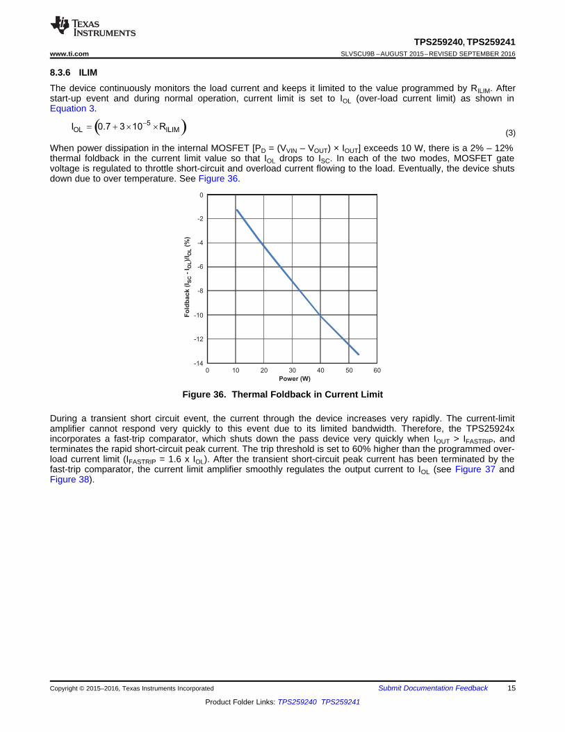
When power dissipation in the internal MOSFET [PD = (VVIN – VOUT) × IOUT] exceeds 10 W, there is a 2% – 12%thermal foldback in the current limit value so that IOL drops to ISC. In each of the two modes, MOSFET gatevoltage is regulated to throttle short-circuit and overload current flowing to the load. Eventually, the device shutsdown due to over temperature. See Figure 36.
Figure 36. Thermal Foldback in Current Limit
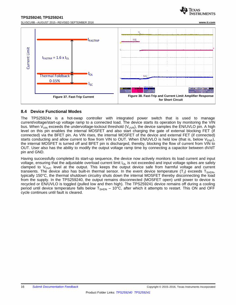
During a transient short circuit event, the current through the device increases very rapidly. The current-limitamplifier cannot respond very quickly to this event due to its limited bandwidth. Therefore, the TPS25924xincorporates a fast-trip comparator, which shuts down the pass device very quickly when IOUT > IFASTRIP, andterminates the rapid short-circuit peak current. The trip threshold is set to 60% higher than the programmed over-load current limit (IFASTRIP = 1.6 x IOL). After the transient short-circuit peak current has been terminated by thefast-trip comparator, the current limit amplifier smoothly regulates the output current to IOL (see Figure 37 andFigure 38).
16
TPS259240, TPS259241SLVSCU9B –AUGUST 2015–REVISED SEPTEMBER 2016 www.ti.com
Product Folder Links: TPS259240 TPS259241
Submit Documentation Feedback Copyright © 2015–2016, Texas Instruments Incorporated
Figure 37. Fast-Trip Current Figure 38. Fast-Trip and Current Limit Amplifier Responsefor Short Circuit
8.4 Device Functional ModesThe TPS25924x is a hot-swap controller with integrated power switch that is used to managecurrent/voltage/start-up voltage ramp to a connected load. The device starts its operation by monitoring the VINbus. When VVIN exceeds the undervoltage-lockout threshold (VUVR), the device samples the EN/UVLO pin. A highlevel on this pin enables the internal MOSFET and also start charging the gate of external blocking FET (ifconnected) via the BFET pin. As VIN rises, the internal MOSFET of the device and external FET (if connected)starts conducting and allow current to flow from VIN to OUT. When EN/UVLO is held low (that is, below VENF),the internal MOSFET is turned off and BFET pin is discharged, thereby, blocking the flow of current from VIN toOUT. User also has the ability to modify the output voltage ramp time by connecting a capacitor between dV/dTpin and GND.
Having successfully completed its start-up sequence, the device now actively monitors its load current and inputvoltage, ensuring that the adjustable overload current limit IOL is not exceeded and input voltage spikes are safelyclamped to VOVC level at the output. This keeps the output device safe from harmful voltage and currenttransients. The device also has built-in thermal sensor. In the event device temperature (TJ) exceeds TSHDN,typically 150°C, the thermal shutdown circuitry shuts down the internal MOSFET thereby disconnecting the loadfrom the supply. In the TPS259240, the output remains disconnected (MOSFET open) until power to device isrecycled or EN/UVLO is toggled (pulled low and then high). The TPS259241 device remains off during a coolingperiod until device temperature falls below TSHDN – 10°C, after which it attempts to restart. This ON and OFFcycle continues until fault is cleared.
CVIN
0.1µFCOUT
1µF
R1
1MO
28mO
IN OUT
EN/UVLO
dVdT
GNDTPS25924x
ILIM
VOUT, IOUT < 3.4A
RILIM
100kO*Optional & only for noise suppression
*
VIN = 4.5 to 18 V
R2
**Optional & only needed for external UVLO
**BFET
17
TPS259240, TPS259241www.ti.com SLVSCU9B –AUGUST 2015–REVISED SEPTEMBER 2016
Product Folder Links: TPS259240 TPS259241
Submit Documentation FeedbackCopyright © 2015–2016, Texas Instruments Incorporated
9 Application and Implementation
NOTEInformation in the following applications sections is not part of the TI componentspecification, and TI does not warrant its accuracy or completeness. TI’s customers areresponsible for determining suitability of components for their purposes. Customers shouldvalidate and test their design implementation to confirm system functionality.
9.1 Application InformationThe TPS25924x is a smart eFuse. It is typically used for Hot-Swap and Power rail protection applications. Itoperates from 4.5 V to 18 V with programmable current limit and undervoltage protection. The device aids incontrolling the in-rush current and provides precise current limiting during overload conditions for systems suchas Set-Top-Box, DTVs, Gaming Consoles, SSDs/HDDs and Smart Meters. The device also provides robustprotection for multiple faults on the sub-system rail.
The following design procedure can be used to select component values for the device. Alternatively, theWEBENCH® software may be used to generate a complete design. The WEBENCH® software uses an iterativedesign procedure and accesses a comprehensive database of components when generating a design.Additionally, a spreadsheet design tool TPS2592xx Design Calculator (SLUC570) is available on web folder. Thissection presents a simplified discussion of the design process.
9.2 Typical Applications
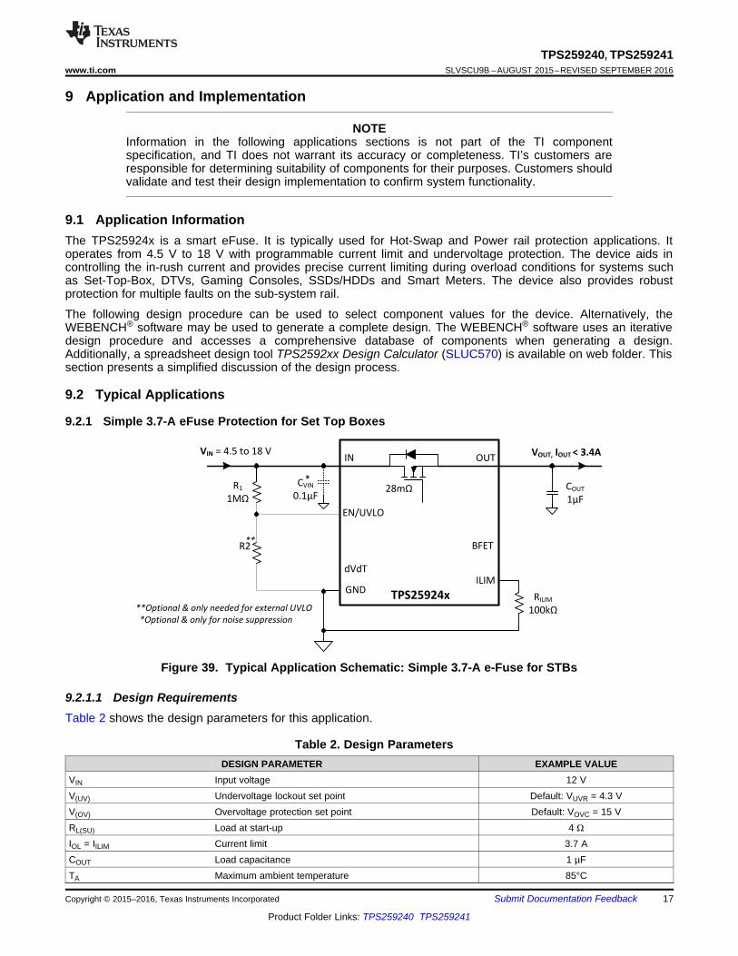
9.2.1 Simple 3.7-A eFuse Protection for Set Top Boxes
Figure 39. Typical Application Schematic: Simple 3.7-A e-Fuse for STBs
9.2.1.1 Design RequirementsTable 2 shows the design parameters for this application.
Table 2. Design ParametersDESIGN PARAMETER EXAMPLE VALUE
VIN Input voltage 12 VV(UV) Undervoltage lockout set point Default: VUVR = 4.3 VV(OV) Overvoltage protection set point Default: VOVC = 15 VRL(SU) Load at start-up 4 Ω
IOL = IILIM Current limit 3.7 ACOUT Load capacitance 1 µFTA Maximum ambient temperature 85°C
(IN)(INRUSH) (OUT)
dVdT
VI C x
T=
1 2(UV) ENR
2
R RV V
R
+= ´
ILIMILIM -5
I - 0.7R =
3 x 10
18
TPS259240, TPS259241SLVSCU9B –AUGUST 2015–REVISED SEPTEMBER 2016 www.ti.com
Product Folder Links: TPS259240 TPS259241
Submit Documentation Feedback Copyright © 2015–2016, Texas Instruments Incorporated
9.2.1.2 Detailed Design ProcedureThe following design procedure can be used to select component values for the TPS25924x.
9.2.1.2.1 Step by Step Design Procedure
This design procedure below seeks to control the junction temperature of device under both static and transientconditions by proper selection of output ramp-up time and associated support components. The designer canadjust this procedure to fit the application and design criteria.
9.2.1.2.2 Programming the Current-Limit Threshold: RILIM Selection
The RILIM resistor at the ILIM pin sets the over load current limit, this can be set using Equation 4.
(4)
For IOL= IILIM = 3.7 A, from Equation 4, RILIM = 100 kΩ, choose closest standard value resistor with 1% tolerance.
9.2.1.2.3 Undervoltage Lockout Set Point
The undervoltage lockout (UVLO) trip point is adjusted using the external voltage divider network of R1 and R2 asconnected between IN, EN/UVLO and GND pins of the device. The values required for setting the undervoltageare calculated solving Equation 5.
(5)
Where VENR = 1.4 V is enable voltage rising threshold.
Since R1 and R2 leak the current from input supply (VIN), these resistors must be selected based on theacceptable leakage current from input power supply (VIN). The current drawnby R1 and R2 from the powersupply IR12 = VIN/(R1 + R2).
However, leakage currents due to external active components connected to the resistor string can add error tothese calculations. So, the resistor string current, IR12 must be chosen to be 20x greater than the leakage currentexpected.
For default UVLO of VUVR = 4.3 V, select R2 = OPEN, and R1 = 1 MΩ. Since EN/UVLO pin is rated only to 7 V, itcannot be connected directly to VIN= 12 V. It has to be connected through R1 = 1 MΩ only, so that the pull-upcurrent for EN/UVLO pin is limited to < 20 µA.
The power failure threshold is detected on the falling edge of supply. This threshold voltage is 4% lower than therising threshold, VUVR. This is calculated using Equation 6.
V(PFAIL) = 0.96 x VUVR (6)
Where VUVR is 4.3 V, Power fail threshold set is 4.1 V.
9.2.1.2.4 Setting Output Voltage Ramp Time (TdVdT)
For a successful design, the junction temperature of device must be kept below the absolute-maximum ratingduring both dynamic (start-up) and steady state conditions. Dynamic power stresses often are an order ofmagnitude greater than the static stresses, so it is important to determine the right start-up time and in-rushcurrent limit required with system capacitance to avoid thermal shutdown during start-up with and without load.
The ramp-up capacitor CdVdT needed is calculated considering the two possible cases:
9.2.1.2.4.1 Case 1: Start-Up without Load: Only Output Capacitance COUT Draws Current During Start-Up
During start-up, as the output capacitor charges, the voltage difference as well as the power dissipated acrossthe internal FET decreases. The average power dissipated in the device during start-up is calculated usingEquation 8.
For TPS25924x, the inrush current is determined as shown in Equation 7:
(7)
(INRUSH)12
= 1 F x = 15 mA840 s
I mm
( )6dVdT = 10 x 12 x 0 + 70 pF 840 sT = m
Power Dissipation (W)
The
rmal
Shu
tdow
n T
ime
(ms)
0.1 1 10 1000.1
1
10
100
1000
10000
D001
TA = -40oCTA = 25oCTA = 85oCTA = 125oC
(INRUSH)OLdVdT(Current-Limited) OUT L(SU)
(IN)(INRUSH)OL
L(SU)
IIT C x R x 1 LN
VII
R
é ùæ ö÷çê ú÷ç ÷çê ú÷ç ÷ê úç ÷ç ÷= - +ê ú÷ç ÷çê ú÷ç ÷ç -ê ú÷ç ÷ê úç ÷çè øë û
(STARTUP) (INRUSH) LI I + I (t)=
D(STARTUP) D(INRUSH) D(LOAD)P P + P=
2(IN)
D(LOAD)L(SU)
V1P x
6 R
æ ö÷ç= ÷ç ÷÷çè ø
D(INRUSH) (IN) (INRUSH)P 0.5 x V x I=
19
TPS259240, TPS259241www.ti.com SLVSCU9B –AUGUST 2015–REVISED SEPTEMBER 2016
Product Folder Links: TPS259240 TPS259241
Submit Documentation FeedbackCopyright © 2015–2016, Texas Instruments Incorporated
Power dissipation during start-up is given by Equation 8:
(8)
Equation 8 assumes that load does not draw any current until the output voltage has reached its final value.
9.2.1.2.4.2 Case 2: Start-Up with Load: Output Capacitance COUT and Load Draws Current During Start-Up
When load draws current during the turnon sequence, there is additional power dissipated. Considering aresistive load during start-up (RL(SU)), load current ramps up proportionally with increase in output voltage duringTdVdT time. The average power dissipation in the internal FET during charging time due to resistive load is givenby Equation 9:
(9)
Total power dissipated in the device during startup is given by Equation 10:
(10)
Total current during startup is given by Equation 11:
(11)
If I(STARTUP) > IOL, the device limits the current to IOL and the current limited charging time is determined byEquation 12:
(12)
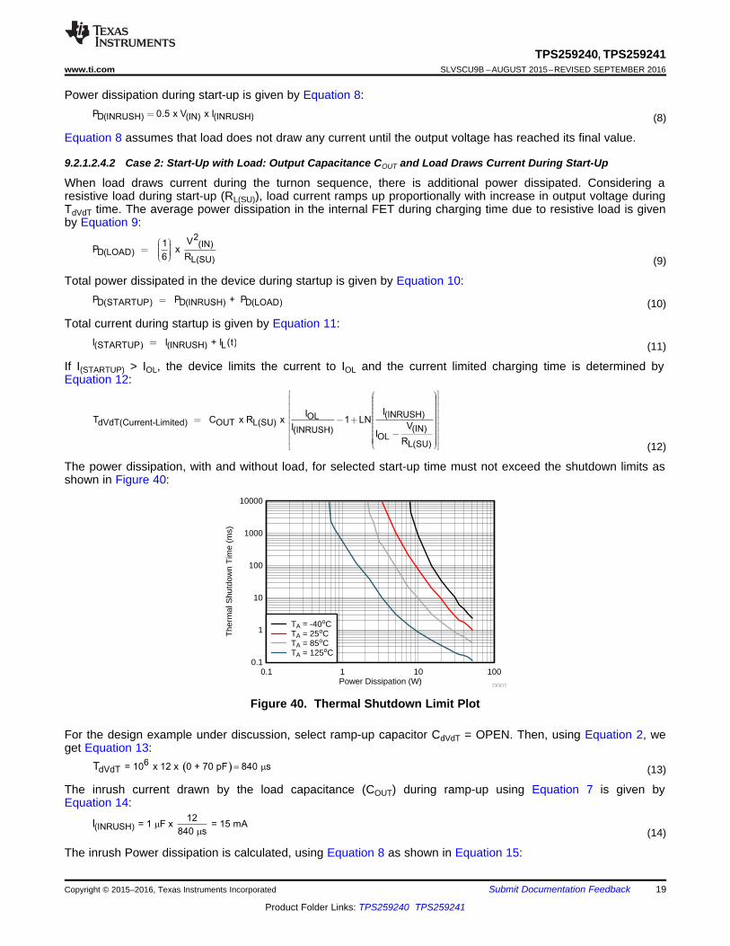
The power dissipation, with and without load, for selected start-up time must not exceed the shutdown limits asshown in Figure 40:
Figure 40. Thermal Shutdown Limit Plot
For the design example under discussion, select ramp-up capacitor CdVdT = OPEN. Then, using Equation 2, weget Equation 13:
(13)
The inrush current drawn by the load capacitance (COUT) during ramp-up using Equation 7 is given byEquation 14:
(14)
The inrush Power dissipation is calculated, using Equation 8 as shown in Equation 15:
28m:
VIN OUT
EN/UVLO
dVdT
GND
BFET
TPS25924x
ILIM
RILIM
76.8k:
CVIN*
0.1PF
VIN
CHOLD-UP
4700PF
CdVdT
22nF
CSD16411
VOUT, IOUT < 2.7A
R1
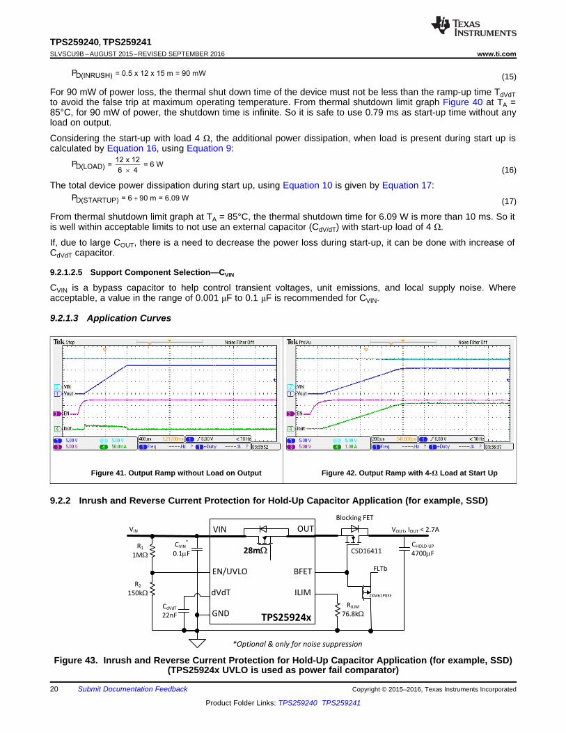
1M:
R2
150k: ZXM61P03F
FLTb
Blocking FET
*Optional & only for noise suppression
D(STARTUP) = 6 90 m = 6.09 WP +
D(LOAD)12 x 12
= = 6 W6 4
P´
D(INRUSH) = 0.5 x 12 x 15 m = 90 mWP
20
TPS259240, TPS259241SLVSCU9B –AUGUST 2015–REVISED SEPTEMBER 2016 www.ti.com
Product Folder Links: TPS259240 TPS259241
Submit Documentation Feedback Copyright © 2015–2016, Texas Instruments Incorporated
(15)
For 90 mW of power loss, the thermal shut down time of the device must not be less than the ramp-up time TdVdTto avoid the false trip at maximum operating temperature. From thermal shutdown limit graph Figure 40 at TA =85°C, for 90 mW of power, the shutdown time is infinite. So it is safe to use 0.79 ms as start-up time without anyload on output.
Considering the start-up with load 4 Ω, the additional power dissipation, when load is present during start up iscalculated by Equation 16, using Equation 9:
(16)
The total device power dissipation during start up, using Equation 10 is given by Equation 17:
(17)
From thermal shutdown limit graph at TA = 85°C, the thermal shutdown time for 6.09 W is more than 10 ms. So itis well within acceptable limits to not use an external capacitor (CdV/dT) with start-up load of 4 Ω.
If, due to large COUT, there is a need to decrease the power loss during start-up, it can be done with increase ofCdVdT capacitor.
9.2.1.2.5 Support Component Selection—CVIN
CVIN is a bypass capacitor to help control transient voltages, unit emissions, and local supply noise. Whereacceptable, a value in the range of 0.001 μF to 0.1 μF is recommended for CVIN.
9.2.1.3 Application Curves
Figure 41. Output Ramp without Load on Output Figure 42. Output Ramp with 4-Ω Load at Start Up
9.2.2 Inrush and Reverse Current Protection for Hold-Up Capacitor Application (for example, SSD)
Figure 43. Inrush and Reverse Current Protection for Hold-Up Capacitor Application (for example, SSD)(TPS25924x UVLO is used as power fail comparator)
D(STARTUP) = 1278 24 = 1302 mWP +
D(LOAD)12 x 12
= = 24 mW6 1000
P´
D(INRUSH) = 0.5 x 12 x 213 m = 1278 mWP
(INRUSH)12
= 4700 F x = 213 mA265 ms
I m
( )6dVdT = 10 x 12 x 22 nF + 70 pF 265 msT =
21
TPS259240, TPS259241www.ti.com SLVSCU9B –AUGUST 2015–REVISED SEPTEMBER 2016
Product Folder Links: TPS259240 TPS259241
Submit Documentation FeedbackCopyright © 2015–2016, Texas Instruments Incorporated
9.2.2.1 Design RequirementsThe design parameters for this design example are shown in Table 3.
Table 3. Design ParametersDESIGN PARAMETER EXAMPLE VALUE
VIN Input voltage 12 VV(UV) Undervoltage lockout set point 10.8 VV(OV) Overvoltage protection set point Default: VOVC = 15 VRL(SU) Load at start-up 1000 Ω
IOL= IILIM Current limit 3 ACOUT Load capacitance 4700 µFTA Maximum ambient temperature 85°C
9.2.2.2 Detailed Design Procedure
9.2.2.2.1 Programming the Current-Limit Threshold: RILIM Selection
The RILIM resistor at the ILIM pin sets the over load current limit, this can be set using Equation 4.
For IOL = IILIM = 3 A, from Equation 4, RILIM = 76.8 kΩ. Choose closest standard value resistor with 1% tolerance.
9.2.2.2.2 Undervoltage Lockout Set Point
The undervoltage lockout (UVLO) trip point is adjusted using the external voltage divider network of R1 and R2 asconnected between IN, EN/UVLO and GND pins of the device. The values required for setting the undervoltageare calculated solving Equation 5.
For UVLO of V(UV) = 10.8 V, select R2 = 150 kΩ, and R1 = 1 MΩ.
The power failure threshold is detected on the falling edge of supply. This threshold voltage is 4% lower than therising threshold, V(UV). This is calculated using Equation 6.
Where V(UV) = 10.73 V, Power fail threshold set is V(PFAIL) = 10.35 V.
9.2.2.2.3 Setting Output Voltage Ramp Time (TdVdT)
For a successful design, the junction temperature of device must be kept below the absolute-maximum ratingduring both dynamic (start-up) and steady state conditions. Dynamic power stresses often are an order ofmagnitude greater than the static stresses, so it is important to determine the right start-up time and in-rushcurrent limit required with system capacitance to avoid thermal shutdown during start-up with and without load.
For the design example under discussion, select ramp-up capacitor CdVdT = 22 nF. Then, using Equation 2 weget Equation 18:
(18)
The inrush current drawn by the load capacitance (COUT) during ramp-up using Equation 7 is given byEquation 19:
(19)
The inrush Power dissipation is calculated, using Equation 8 is given by Equation 20:
(20)
Considering the start-up with load 1000 Ω, the additional power dissipation, when load is present during start upis calculated, using Equation 9 is given by Equation 21:
(21)
The total device power dissipation during start up is given by Equation 22:
(22)
CdVdT
R1
R2
28m:
VIN OUT
GND TPS25924xILIM
RILIM
*Optional & only for noise suppression
*CIN
COUT
EN/UVLO
BFET
VIN
dVdTQ1
ZXM61P03F
VOUT
RDCHG
22
TPS259240, TPS259241SLVSCU9B –AUGUST 2015–REVISED SEPTEMBER 2016 www.ti.com
Product Folder Links: TPS259240 TPS259241
Submit Documentation Feedback Copyright © 2015–2016, Texas Instruments Incorporated
From thermal shutdown limit graph at TA = 85°C, the thermal shutdown time for 1.3 W is more than 300 ms. Sothe device starts safely.
If CdVdT = 4.7 nF was used, the device must have tried to charge the 4700-µF output cap with inrush current of986 mA in 57.24 ms, dissipating power of 5.94 W. This is outside the safe starting condition of the device, andmust have led the device to enter thermal shutdown during start-up.
9.2.2.3 Application Curves
COUT = CHOLD-UP =4700 µF
CdVdT = 22 nF
Figure 44. Output Ramp Up
COUT = CHOLD-UP =4700 µF
V(PFAIL) = 10.35 V RLOAD = 12 Ω
Figure 45. Hold-up Power When VIN Fails
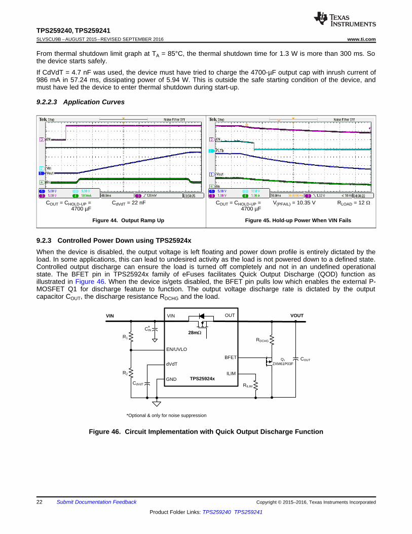
9.2.3 Controlled Power Down using TPS25924xWhen the device is disabled, the output voltage is left floating and power down profile is entirely dictated by theload. In some applications, this can lead to undesired activity as the load is not powered down to a defined state.Controlled output discharge can ensure the load is turned off completely and not in an undefined operationalstate. The BFET pin in TPS25924x family of eFuses facilitates Quick Output Discharge (QOD) function asillustrated in Figure 46. When the device is/gets disabled, the BFET pin pulls low which enables the external P-MOSFET Q1 for discharge feature to function. The output voltage discharge rate is dictated by the outputcapacitor COUT, the discharge resistance RDCHG and the load.
Figure 46. Circuit Implementation with Quick Output Discharge Function
CVIN
0.1µF COUTR1 28mO
IN OUT
EN/UVLO
dVdT
GNDTPS25924x
ILIM
VOUT
RILIM*Optional components for
transient suppression
*
VIN
R2 BFET
* *
CdVdT
(IN)SPIKE(Absolute) (IN) (LOAD)
(IN)
LV V + I x
C=
23
TPS259240, TPS259241www.ti.com SLVSCU9B –AUGUST 2015–REVISED SEPTEMBER 2016
Product Folder Links: TPS259240 TPS259241
Submit Documentation FeedbackCopyright © 2015–2016, Texas Instruments Incorporated
10 Power Supply RecommendationsThe device is designed for supply voltage range of 4.5 V ≤ VIN ≤ 18 V. If the input supply is located more than afew inches from the device an input ceramic bypass capacitor higher than 0.1 μF is recommended. Power supplymust be rated higher than the current limit set to avoid voltage droops during over current and short-circuitconditions.
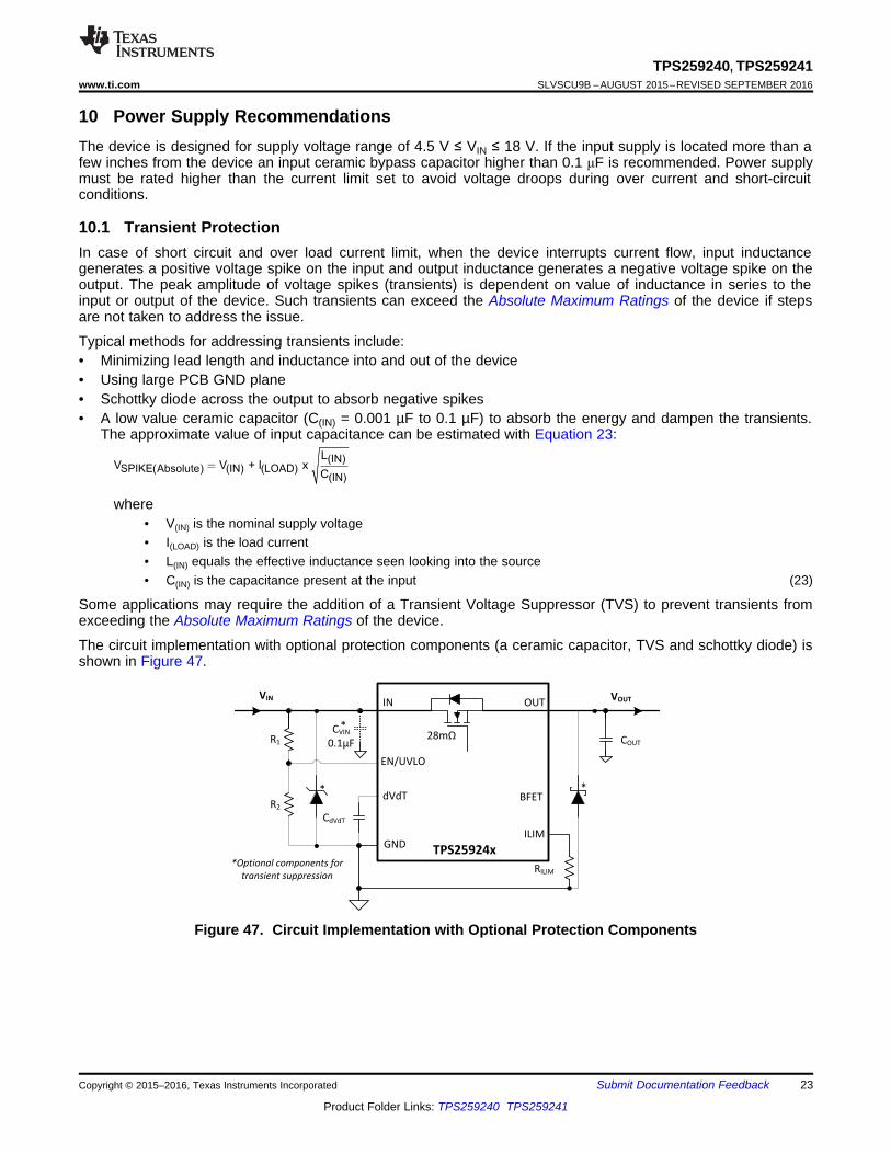
10.1 Transient ProtectionIn case of short circuit and over load current limit, when the device interrupts current flow, input inductancegenerates a positive voltage spike on the input and output inductance generates a negative voltage spike on theoutput. The peak amplitude of voltage spikes (transients) is dependent on value of inductance in series to theinput or output of the device. Such transients can exceed the Absolute Maximum Ratings of the device if stepsare not taken to address the issue.
Typical methods for addressing transients include:• Minimizing lead length and inductance into and out of the device• Using large PCB GND plane• Schottky diode across the output to absorb negative spikes• A low value ceramic capacitor (C(IN) = 0.001 µF to 0.1 µF) to absorb the energy and dampen the transients.
The approximate value of input capacitance can be estimated with Equation 23:
where• V(IN) is the nominal supply voltage• I(LOAD) is the load current• L(IN) equals the effective inductance seen looking into the source• C(IN) is the capacitance present at the input (23)
Some applications may require the addition of a Transient Voltage Suppressor (TVS) to prevent transients fromexceeding the Absolute Maximum Ratings of the device.
The circuit implementation with optional protection components (a ceramic capacitor, TVS and schottky diode) isshown in Figure 47.
Figure 47. Circuit Implementation with Optional Protection Components
24
TPS259240, TPS259241SLVSCU9B –AUGUST 2015–REVISED SEPTEMBER 2016 www.ti.com
Product Folder Links: TPS259240 TPS259241
Submit Documentation Feedback Copyright © 2015–2016, Texas Instruments Incorporated
10.2 Output Short-Circuit MeasurementsIt is difficult to obtain repeatable and similar short-circuit testing results. Source bypassing, input leads, circuitlayout and component selection, output shorting method, relative location of the short, and instrumentation allcontribute to variation in results. The actual short itself exhibits a certain degree of randomness as itmicroscopically bounces and arcs. Care in configuration and methods must be used to obtain realistic results. Donot expect to see waveforms exactly like those in the data sheet; every setup differs.
VIN
VIN
High Frequency
Bypass Capacitor
VOUT
Via to signal ground plane
Top layer
Bottom layer signal ground plane
* Optional: Needed only to suppress the transients caused by inductive load switching
*
6
7
OUT
OUT
8 OUT
9 BFET
ILIM
4
3
VIN
VIN
2EN/UVLO
1dV/dT
5VIN
10 Ground -
Bottom
layer
*
Power Ground
25
TPS259240, TPS259241www.ti.com SLVSCU9B –AUGUST 2015–REVISED SEPTEMBER 2016
Product Folder Links: TPS259240 TPS259241
Submit Documentation FeedbackCopyright © 2015–2016, Texas Instruments Incorporated
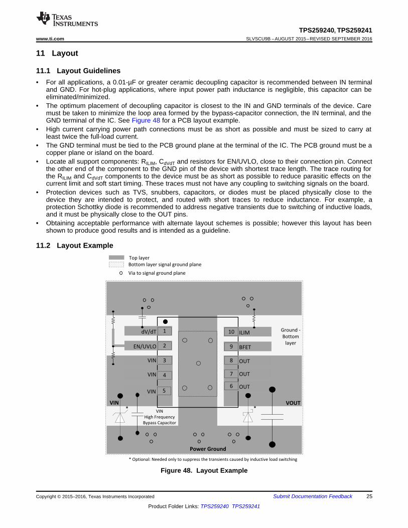
11 Layout
11.1 Layout Guidelines• For all applications, a 0.01-µF or greater ceramic decoupling capacitor is recommended between IN terminal
and GND. For hot-plug applications, where input power path inductance is negligible, this capacitor can beeliminated/minimized.
• The optimum placement of decoupling capacitor is closest to the IN and GND terminals of the device. Caremust be taken to minimize the loop area formed by the bypass-capacitor connection, the IN terminal, and theGND terminal of the IC. See Figure 48 for a PCB layout example.
• High current carrying power path connections must be as short as possible and must be sized to carry atleast twice the full-load current.
• The GND terminal must be tied to the PCB ground plane at the terminal of the IC. The PCB ground must be acopper plane or island on the board.
• Locate all support components: RILIM, CdVdT and resistors for EN/UVLO, close to their connection pin. Connectthe other end of the component to the GND pin of the device with shortest trace length. The trace routing forthe RILIM and CdVdT components to the device must be as short as possible to reduce parasitic effects on thecurrent limit and soft start timing. These traces must not have any coupling to switching signals on the board.
• Protection devices such as TVS, snubbers, capacitors, or diodes must be placed physically close to thedevice they are intended to protect, and routed with short traces to reduce inductance. For example, aprotection Schottky diode is recommended to address negative transients due to switching of inductive loads,and it must be physically close to the OUT pins.
• Obtaining acceptable performance with alternate layout schemes is possible; however this layout has beenshown to produce good results and is intended as a guideline.
11.2 Layout Example
Figure 48. Layout Example
26
TPS259240, TPS259241SLVSCU9B –AUGUST 2015–REVISED SEPTEMBER 2016 www.ti.com
Product Folder Links: TPS259240 TPS259241
Submit Documentation Feedback Copyright © 2015–2016, Texas Instruments Incorporated
12 Device and Documentation Support
12.1 Device Support
12.1.1 Third-Party Products DisclaimerTI'S PUBLICATION OF INFORMATION REGARDING THIRD-PARTY PRODUCTS OR SERVICES DOES NOTCONSTITUTE AN ENDORSEMENT REGARDING THE SUITABILITY OF SUCH PRODUCTS OR SERVICESOR A WARRANTY, REPRESENTATION OR ENDORSEMENT OF SUCH PRODUCTS OR SERVICES, EITHERALONE OR IN COMBINATION WITH ANY TI PRODUCT OR SERVICE.
12.2 Documentation Support
12.2.1 Related DocumentationFor related documentation see the following:• TPS2592xx Design Calculator• TPS259230-41EVM User's Guide
12.3 Related LinksThe table below lists quick access links. Categories include technical documents, support and communityresources, tools and software, and quick access to sample or buy.
Table 4. Related Links
PARTS PRODUCT FOLDER SAMPLE & BUY TECHNICALDOCUMENTS
TOOLS &SOFTWARE
SUPPORT &COMMUNITY
TPS259241 Click here Click here Click here Click here Click hereTPS259240 Click here Click here Click here Click here Click here
12.4 Receiving Notification of Documentation UpdatesTo receive notification of documentation updates, navigate to the device product folder on ti.com. In the upperright corner, click on Alert me to register and receive a weekly digest of any product information that haschanged. For change details, review the revision history included in any revised document.
12.5 Community ResourcesThe following links connect to TI community resources. Linked contents are provided "AS IS" by the respectivecontributors. They do not constitute TI specifications and do not necessarily reflect TI's views; see TI's Terms ofUse.
TI E2E™ Online Community TI's Engineer-to-Engineer (E2E) Community. Created to foster collaborationamong engineers. At e2e.ti.com, you can ask questions, share knowledge, explore ideas and helpsolve problems with fellow engineers.
Design Support TI's Design Support Quickly find helpful E2E forums along with design support tools andcontact information for technical support.
12.6 TrademarksE2E is a trademark of Texas Instruments.WEBENCH is a registered trademark of Texas Instruments.All other trademarks are the property of their respective owners.
12.7 Electrostatic Discharge CautionThis integrated circuit can be damaged by ESD. Texas Instruments recommends that all integrated circuits be handled withappropriate precautions. Failure to observe proper handling and installation procedures can cause damage.
ESD damage can range from subtle performance degradation to complete device failure. Precision integrated circuits may be moresusceptible to damage because very small parametric changes could cause the device not to meet its published specifications.
27
TPS259240, TPS259241www.ti.com SLVSCU9B –AUGUST 2015–REVISED SEPTEMBER 2016
Product Folder Links: TPS259240 TPS259241
Submit Documentation FeedbackCopyright © 2015–2016, Texas Instruments Incorporated
12.8 GlossarySLYZ022 — TI Glossary.
This glossary lists and explains terms, acronyms, and definitions.
13 Mechanical, Packaging, and Orderable InformationThe following pages include mechanical, packaging, and orderable information. This information is the mostcurrent data available for the designated devices. This data is subject to change without notice and revision ofthis document. For browser-based versions of this data sheet, refer to the left-hand navigation.
PACKAGE OPTION ADDENDUM
www.ti.com 2-Sep-2016
Addendum-Page 1
PACKAGING INFORMATION
Orderable Device Status(1)
Package Type PackageDrawing
Pins PackageQty
Eco Plan(2)
Lead/Ball Finish(6)
MSL Peak Temp(3)
Op Temp (°C) Device Marking(4/5)
Samples
TPS259240DRCR ACTIVE VSON DRC 10 3000 Green (RoHS& no Sb/Br)
CU NIPDAU Level-2-260C-1 YEAR -40 to 85 259240
TPS259240DRCT ACTIVE VSON DRC 10 250 Green (RoHS& no Sb/Br)
CU NIPDAU Level-2-260C-1 YEAR -40 to 85 259240
TPS259241DRCR ACTIVE VSON DRC 10 3000 Green (RoHS& no Sb/Br)
CU NIPDAU Level-2-260C-1 YEAR -40 to 85 259241
TPS259241DRCT ACTIVE VSON DRC 10 250 Green (RoHS& no Sb/Br)
CU NIPDAU Level-2-260C-1 YEAR -40 to 85 259241
(1) The marketing status values are defined as follows:ACTIVE: Product device recommended for new designs.LIFEBUY: TI has announced that the device will be discontinued, and a lifetime-buy period is in effect.NRND: Not recommended for new designs. Device is in production to support existing customers, but TI does not recommend using this part in a new design.PREVIEW: Device has been announced but is not in production. Samples may or may not be available.OBSOLETE: TI has discontinued the production of the device.
(2) Eco Plan - The planned eco-friendly classification: Pb-Free (RoHS), Pb-Free (RoHS Exempt), or Green (RoHS & no Sb/Br) - please check http://www.ti.com/productcontent for the latest availabilityinformation and additional product content details.TBD: The Pb-Free/Green conversion plan has not been defined.Pb-Free (RoHS): TI's terms "Lead-Free" or "Pb-Free" mean semiconductor products that are compatible with the current RoHS requirements for all 6 substances, including the requirement thatlead not exceed 0.1% by weight in homogeneous materials. Where designed to be soldered at high temperatures, TI Pb-Free products are suitable for use in specified lead-free processes.Pb-Free (RoHS Exempt): This component has a RoHS exemption for either 1) lead-based flip-chip solder bumps used between the die and package, or 2) lead-based die adhesive used betweenthe die and leadframe. The component is otherwise considered Pb-Free (RoHS compatible) as defined above.Green (RoHS & no Sb/Br): TI defines "Green" to mean Pb-Free (RoHS compatible), and free of Bromine (Br) and Antimony (Sb) based flame retardants (Br or Sb do not exceed 0.1% by weightin homogeneous material)
(3) MSL, Peak Temp. - The Moisture Sensitivity Level rating according to the JEDEC industry standard classifications, and peak solder temperature.
(4) There may be additional marking, which relates to the logo, the lot trace code information, or the environmental category on the device.
(5) Multiple Device Markings will be inside parentheses. Only one Device Marking contained in parentheses and separated by a "~" will appear on a device. If a line is indented then it is a continuationof the previous line and the two combined represent the entire Device Marking for that device.
(6) Lead/Ball Finish - Orderable Devices may have multiple material finish options. Finish options are separated by a vertical ruled line. Lead/Ball Finish values may wrap to two lines if the finishvalue exceeds the maximum column width.
PACKAGE OPTION ADDENDUM
www.ti.com 2-Sep-2016
Addendum-Page 2
Important Information and Disclaimer:The information provided on this page represents TI's knowledge and belief as of the date that it is provided. TI bases its knowledge and belief on informationprovided by third parties, and makes no representation or warranty as to the accuracy of such information. Efforts are underway to better integrate information from third parties. TI has taken andcontinues to take reasonable steps to provide representative and accurate information but may not have conducted destructive testing or chemical analysis on incoming materials and chemicals.TI and TI suppliers consider certain information to be proprietary, and thus CAS numbers and other limited information may not be available for release.
In no event shall TI's liability arising out of such information exceed the total purchase price of the TI part(s) at issue in this document sold by TI to Customer on an annual basis.
TAPE AND REEL INFORMATION
*All dimensions are nominal
Device PackageType
PackageDrawing
Pins SPQ ReelDiameter
(mm)
ReelWidth
W1 (mm)
A0(mm)
B0(mm)
K0(mm)
P1(mm)
W(mm)
Pin1Quadrant
TPS259240DRCR VSON DRC 10 3000 330.0 12.4 3.3 3.3 1.1 8.0 12.0 Q2
TPS259240DRCR VSON DRC 10 3000 330.0 12.4 3.3 3.3 1.1 8.0 12.0 Q2
TPS259240DRCT VSON DRC 10 250 180.0 12.4 3.3 3.3 1.1 8.0 12.0 Q2
TPS259240DRCT VSON DRC 10 250 180.0 12.4 3.3 3.3 1.1 8.0 12.0 Q2
TPS259241DRCR VSON DRC 10 3000 330.0 12.4 3.3 3.3 1.1 8.0 12.0 Q2
TPS259241DRCR VSON DRC 10 3000 330.0 12.4 3.3 3.3 1.1 8.0 12.0 Q2
TPS259241DRCT VSON DRC 10 250 180.0 12.4 3.3 3.3 1.1 8.0 12.0 Q2
TPS259241DRCT VSON DRC 10 250 180.0 12.4 3.3 3.3 1.1 8.0 12.0 Q2
PACKAGE MATERIALS INFORMATION
www.ti.com 30-Apr-2018
Pack Materials-Page 1
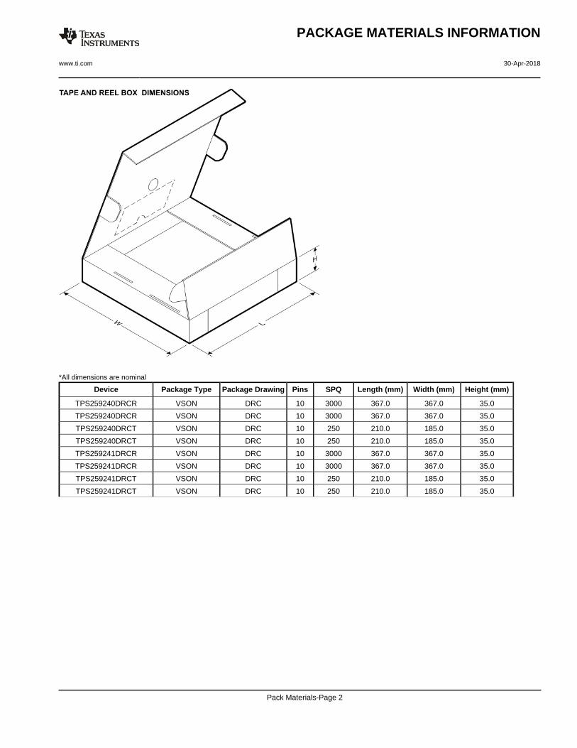
*All dimensions are nominal
Device Package Type Package Drawing Pins SPQ Length (mm) Width (mm) Height (mm)
TPS259240DRCR VSON DRC 10 3000 367.0 367.0 35.0
TPS259240DRCR VSON DRC 10 3000 367.0 367.0 35.0
TPS259240DRCT VSON DRC 10 250 210.0 185.0 35.0
TPS259240DRCT VSON DRC 10 250 210.0 185.0 35.0
TPS259241DRCR VSON DRC 10 3000 367.0 367.0 35.0
TPS259241DRCR VSON DRC 10 3000 367.0 367.0 35.0
TPS259241DRCT VSON DRC 10 250 210.0 185.0 35.0
TPS259241DRCT VSON DRC 10 250 210.0 185.0 35.0
PACKAGE MATERIALS INFORMATION
www.ti.com 30-Apr-2018
Pack Materials-Page 2
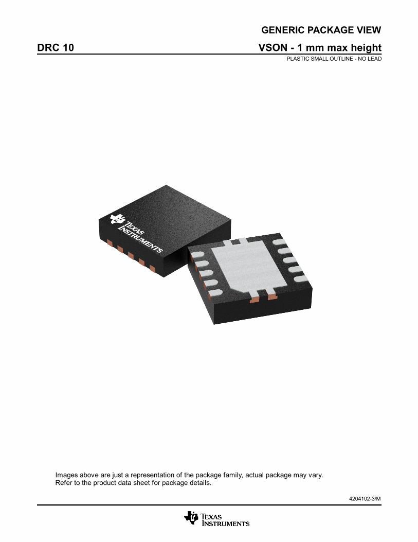
GENERIC PACKAGE VIEW
Images above are just a representation of the package family, actual package may vary.Refer to the product data sheet for package details.
DRC 10 VSON - 1 mm max heightPLASTIC SMALL OUTLINE - NO LEAD
4204102-3/M
www.ti.com
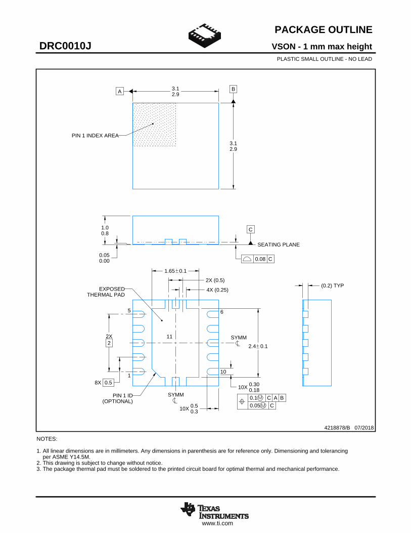
PACKAGE OUTLINE
C
10X 0.300.18
2.4 0.1
2X2
1.65 0.1
8X 0.5
1.00.8
10X 0.50.3
0.050.00
A 3.12.9
B
3.12.9
(0.2) TYP4X (0.25)
2X (0.5)
VSON - 1 mm max heightDRC0010JPLASTIC SMALL OUTLINE - NO LEAD
4218878/B 07/2018
PIN 1 INDEX AREA
SEATING PLANE
0.08 C
1
5 6
10
(OPTIONAL)PIN 1 ID 0.1 C A B
0.05 C
THERMAL PADEXPOSED
SYMM
SYMM11
NOTES: 1. All linear dimensions are in millimeters. Any dimensions in parenthesis are for reference only. Dimensioning and tolerancing per ASME Y14.5M. 2. This drawing is subject to change without notice. 3. The package thermal pad must be soldered to the printed circuit board for optimal thermal and mechanical performance.
SCALE 4.000
www.ti.com
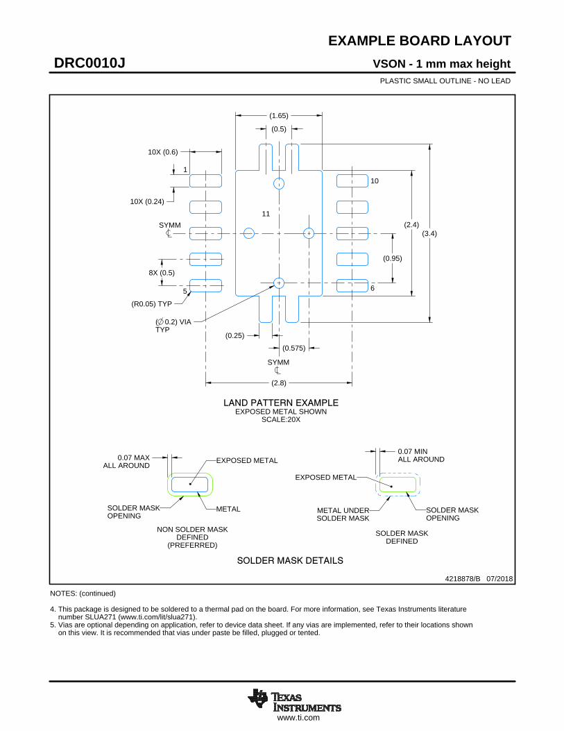
EXAMPLE BOARD LAYOUT
0.07 MINALL AROUND0.07 MAX
ALL AROUND
10X (0.24)
(2.4)
(2.8)
8X (0.5)
(1.65)
( 0.2) VIATYP
(0.575)
(0.95)
10X (0.6)
(R0.05) TYP
(3.4)
(0.25)
(0.5)
VSON - 1 mm max heightDRC0010JPLASTIC SMALL OUTLINE - NO LEAD
4218878/B 07/2018
SYMM
1
5 6
10
LAND PATTERN EXAMPLEEXPOSED METAL SHOWN
SCALE:20X
11SYMM
NOTES: (continued) 4. This package is designed to be soldered to a thermal pad on the board. For more information, see Texas Instruments literature number SLUA271 (www.ti.com/lit/slua271).5. Vias are optional depending on application, refer to device data sheet. If any vias are implemented, refer to their locations shown on this view. It is recommended that vias under paste be filled, plugged or tented.
SOLDER MASKOPENINGSOLDER MASK
METAL UNDER
SOLDER MASKDEFINED
EXPOSED METAL
METALSOLDER MASKOPENING
SOLDER MASK DETAILS
NON SOLDER MASKDEFINED
(PREFERRED)
EXPOSED METAL
www.ti.com
EXAMPLE STENCIL DESIGN
(R0.05) TYP
10X (0.24)
10X (0.6)
2X (1.5)
2X(1.06)
(2.8)
(0.63)
8X (0.5)
(0.5)
4X (0.34)
4X (0.25)
(1.53)
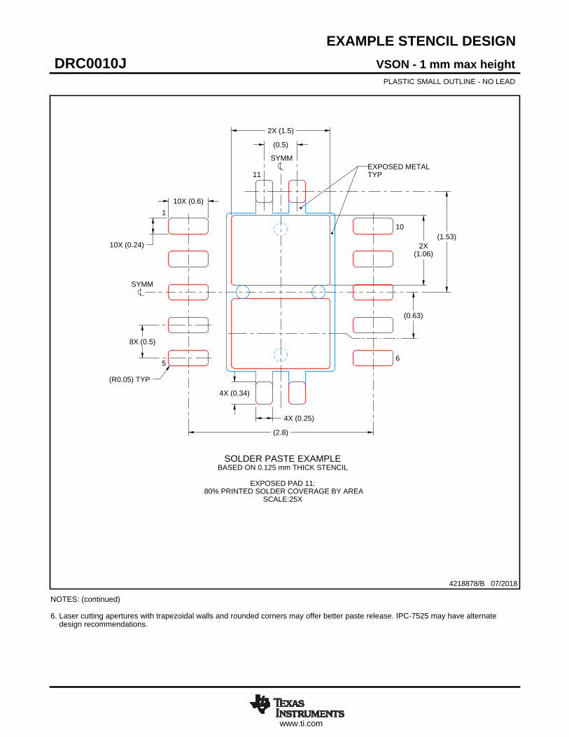
VSON - 1 mm max heightDRC0010JPLASTIC SMALL OUTLINE - NO LEAD
4218878/B 07/2018
NOTES: (continued) 6. Laser cutting apertures with trapezoidal walls and rounded corners may offer better paste release. IPC-7525 may have alternate design recommendations.
SOLDER PASTE EXAMPLEBASED ON 0.125 mm THICK STENCIL
EXPOSED PAD 11:
80% PRINTED SOLDER COVERAGE BY AREASCALE:25X
SYMM
1
56
10
EXPOSED METALTYP11
SYMM
IMPORTANT NOTICE
Texas Instruments Incorporated (TI) reserves the right to make corrections, enhancements, improvements and other changes to itssemiconductor products and services per JESD46, latest issue, and to discontinue any product or service per JESD48, latest issue. Buyersshould obtain the latest relevant information before placing orders and should verify that such information is current and complete.TI’s published terms of sale for semiconductor products (http://www.ti.com/sc/docs/stdterms.htm) apply to the sale of packaged integratedcircuit products that TI has qualified and released to market. Additional terms may apply to the use or sale of other types of TI products andservices.Reproduction of significant portions of TI information in TI data sheets is permissible only if reproduction is without alteration and isaccompanied by all associated warranties, conditions, limitations, and notices. TI is not responsible or liable for such reproduceddocumentation. Information of third parties may be subject to additional restrictions. Resale of TI products or services with statementsdifferent from or beyond the parameters stated by TI for that product or service voids all express and any implied warranties for theassociated TI product or service and is an unfair and deceptive business practice. TI is not responsible or liable for any such statements.Buyers and others who are developing systems that incorporate TI products (collectively, “Designers”) understand and agree that Designersremain responsible for using their independent analysis, evaluation and judgment in designing their applications and that Designers havefull and exclusive responsibility to assure the safety of Designers' applications and compliance of their applications (and of all TI productsused in or for Designers’ applications) with all applicable regulations, laws and other applicable requirements. Designer represents that, withrespect to their applications, Designer has all the necessary expertise to create and implement safeguards that (1) anticipate dangerousconsequences of failures, (2) monitor failures and their consequences, and (3) lessen the likelihood of failures that might cause harm andtake appropriate actions. Designer agrees that prior to using or distributing any applications that include TI products, Designer willthoroughly test such applications and the functionality of such TI products as used in such applications.TI’s provision of technical, application or other design advice, quality characterization, reliability data or other services or information,including, but not limited to, reference designs and materials relating to evaluation modules, (collectively, “TI Resources”) are intended toassist designers who are developing applications that incorporate TI products; by downloading, accessing or using TI Resources in anyway, Designer (individually or, if Designer is acting on behalf of a company, Designer’s company) agrees to use any particular TI Resourcesolely for this purpose and subject to the terms of this Notice.TI’s provision of TI Resources does not expand or otherwise alter TI’s applicable published warranties or warranty disclaimers for TIproducts, and no additional obligations or liabilities arise from TI providing such TI Resources. TI reserves the right to make corrections,enhancements, improvements and other changes to its TI Resources. TI has not conducted any testing other than that specificallydescribed in the published documentation for a particular TI Resource.Designer is authorized to use, copy and modify any individual TI Resource only in connection with the development of applications thatinclude the TI product(s) identified in such TI Resource. NO OTHER LICENSE, EXPRESS OR IMPLIED, BY ESTOPPEL OR OTHERWISETO ANY OTHER TI INTELLECTUAL PROPERTY RIGHT, AND NO LICENSE TO ANY TECHNOLOGY OR INTELLECTUAL PROPERTYRIGHT OF TI OR ANY THIRD PARTY IS GRANTED HEREIN, including but not limited to any patent right, copyright, mask work right, orother intellectual property right relating to any combination, machine, or process in which TI products or services are used. Informationregarding or referencing third-party products or services does not constitute a license to use such products or services, or a warranty orendorsement thereof. Use of TI Resources may require a license from a third party under the patents or other intellectual property of thethird party, or a license from TI under the patents or other intellectual property of TI.TI RESOURCES ARE PROVIDED “AS IS” AND WITH ALL FAULTS. TI DISCLAIMS ALL OTHER WARRANTIES ORREPRESENTATIONS, EXPRESS OR IMPLIED, REGARDING RESOURCES OR USE THEREOF, INCLUDING BUT NOT LIMITED TOACCURACY OR COMPLETENESS, TITLE, ANY EPIDEMIC FAILURE WARRANTY AND ANY IMPLIED WARRANTIES OFMERCHANTABILITY, FITNESS FOR A PARTICULAR PURPOSE, AND NON-INFRINGEMENT OF ANY THIRD PARTY INTELLECTUALPROPERTY RIGHTS. TI SHALL NOT BE LIABLE FOR AND SHALL NOT DEFEND OR INDEMNIFY DESIGNER AGAINST ANY CLAIM,INCLUDING BUT NOT LIMITED TO ANY INFRINGEMENT CLAIM THAT RELATES TO OR IS BASED ON ANY COMBINATION OFPRODUCTS EVEN IF DESCRIBED IN TI RESOURCES OR OTHERWISE. IN NO EVENT SHALL TI BE LIABLE FOR ANY ACTUAL,DIRECT, SPECIAL, COLLATERAL, INDIRECT, PUNITIVE, INCIDENTAL, CONSEQUENTIAL OR EXEMPLARY DAMAGES INCONNECTION WITH OR ARISING OUT OF TI RESOURCES OR USE THEREOF, AND REGARDLESS OF WHETHER TI HAS BEENADVISED OF THE POSSIBILITY OF SUCH DAMAGES.Unless TI has explicitly designated an individual product as meeting the requirements of a particular industry standard (e.g., ISO/TS 16949and ISO 26262), TI is not responsible for any failure to meet such industry standard requirements.Where TI specifically promotes products as facilitating functional safety or as compliant with industry functional safety standards, suchproducts are intended to help enable customers to design and create their own applications that meet applicable functional safety standardsand requirements. Using products in an application does not by itself establish any safety features in the application. Designers mustensure compliance with safety-related requirements and standards applicable to their applications. Designer may not use any TI products inlife-critical medical equipment unless authorized officers of the parties have executed a special contract specifically governing such use.Life-critical medical equipment is medical equipment where failure of such equipment would cause serious bodily injury or death (e.g., lifesupport, pacemakers, defibrillators, heart pumps, neurostimulators, and implantables). Such equipment includes, without limitation, allmedical devices identified by the U.S. Food and Drug Administration as Class III devices and equivalent classifications outside the U.S.TI may expressly designate certain products as completing a particular qualification (e.g., Q100, Military Grade, or Enhanced Product).Designers agree that it has the necessary expertise to select the product with the appropriate qualification designation for their applicationsand that proper product selection is at Designers’ own risk. Designers are solely responsible for compliance with all legal and regulatoryrequirements in connection with such selection.Designer will fully indemnify TI and its representatives against any damages, costs, losses, and/or liabilities arising out of Designer’s non-compliance with the terms and provisions of this Notice.
Mailing Address: Texas Instruments, Post Office Box 655303, Dallas, Texas 75265Copyright © 2018, Texas Instruments Incorporated


![1.6L 4-CYL - VIN [A] & 1.8L 4-CYL - VIN [A]](https://img.pdfslide.us/doc/110x75/61789fad5dd459523072558c/16l-4-cyl-vin-a-amp-18l-4-cyl-vin-a.jpg)