Embed Size (px)
Citation preview
R19DS0069EJ0107 Rev. 1.07 page 1 of 40 Jul 30th, 2018
Datasheet
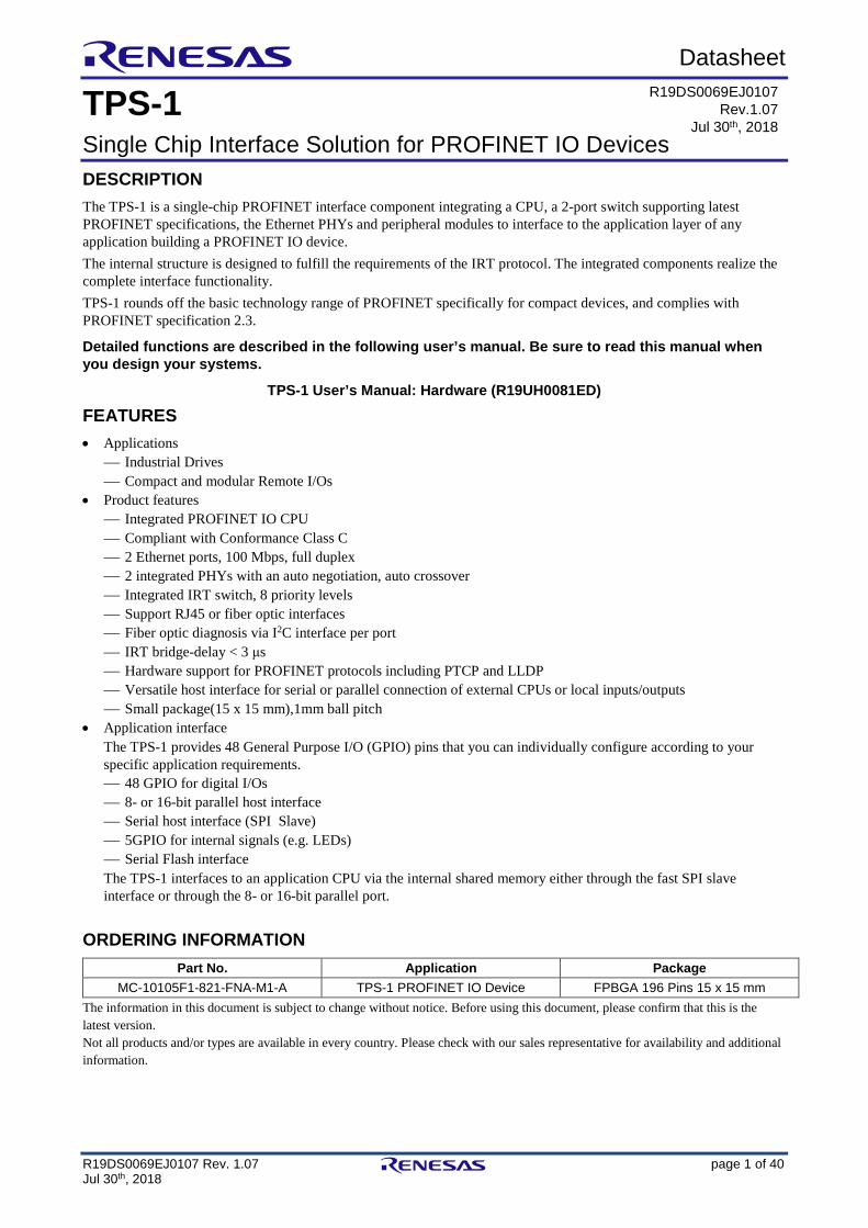
TPS-1 Single Chip Interface Solution for PROFINET IO Devices DESCRIPTION The TPS-1 is a single-chip PROFINET interface component integrating a CPU, a 2-port switch supporting latest PROFINET specifications, the Ethernet PHYs and peripheral modules to interface to the application layer of any application building a PROFINET IO device. The internal structure is designed to fulfill the requirements of the IRT protocol. The integrated components realize the complete interface functionality. TPS-1 rounds off the basic technology range of PROFINET specifically for compact devices, and complies with PROFINET specification 2.3.
Detailed functions are described in the following user’s manual. Be sure to read this manual when you design your systems.
TPS-1 User’s Manual: Hardware (R19UH0081ED)
FEATURES • Applications
Industrial Drives Compact and modular Remote I/Os
• Product features Integrated PROFINET IO CPU Compliant with Conformance Class C 2 Ethernet ports, 100 Mbps, full duplex 2 integrated PHYs with an auto negotiation, auto crossover Integrated IRT switch, 8 priority levels Support RJ45 or fiber optic interfaces Fiber optic diagnosis via I2C interface per port IRT bridge-delay < 3 μs Hardware support for PROFINET protocols including PTCP and LLDP Versatile host interface for serial or parallel connection of external CPUs or local inputs/outputs Small package(15 x 15 mm),1mm ball pitch
• Application interface The TPS-1 provides 48 General Purpose I/O (GPIO) pins that you can individually configure according to your specific application requirements. 48 GPIO for digital I/Os 8- or 16-bit parallel host interface Serial host interface (SPI Slave) 5GPIO for internal signals (e.g. LEDs) Serial Flash interface The TPS-1 interfaces to an application CPU via the internal shared memory either through the fast SPI slave interface or through the 8- or 16-bit parallel port.
ORDERING INFORMATION Part No. Application Package
MC-10105F1-821-FNA-M1-A TPS-1 PROFINET IO Device FPBGA 196 Pins 15 x 15 mm The information in this document is subject to change without notice. Before using this document, please confirm that this is the latest version. Not all products and/or types are available in every country. Please check with our sales representative for availability and additional information.
R19DS0069EJ0107 Rev.1.07
Jul 30th, 2018
TPS-1 INTERNAL BLOCK DIAGRAM
R19DS0069EJ0107 Rev. 1.07 page 2 of 40 Jul 30th, 2018
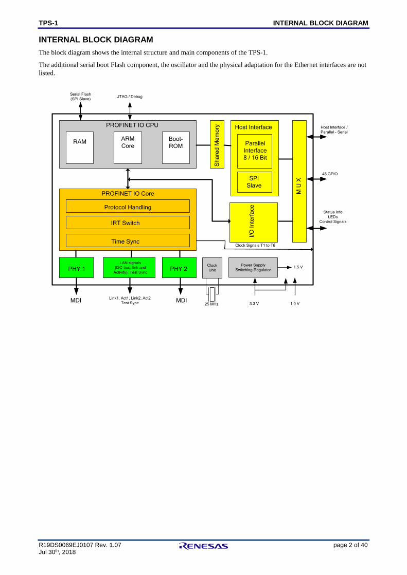
INTERNAL BLOCK DIAGRAM The block diagram shows the internal structure and main components of the TPS-1.
The additional serial boot Flash component, the oscillator and the physical adaptation for the Ethernet interfaces are not listed.
Sha
red
Mem
ory
I/O In
terfa
ce
PHY 2PHY 1
SPISlave
ParallelInterface8 / 16 Bit
Host Interface
M U
X
PROFINET IO CPU
Boot-ROM
ARMCore
RAM
PROFINET IO Core
Time Sync
IRT Switch
Protocol Handling
LAN signals(I2C-bus, link and
Activity), Test Sync
Clock Signals T1 to T6
Clock Unit
25 MHzMDI MDILink1, Act1, Link2, Act2
Test Sync
JTAG / DebugSerial Flash(SPI Slave)
Host Interface /Parallel - Serial
48 GPIO
Status InfoLEDs
Control Signals
Power SupplySwitching Regulator
1.0 V3.3 V
1.5 V
TPS-1 PIN IDENTIFICATION
R19DS0069EJ0107 Rev. 1.07 page 3 of 40 Jul 30th, 2018
PIN IDENTIFICATION SPI Master for Boot Flash ROM
CS_FLASH_OUT : FW Flash: Chip Select
SPI3_SCLK_OUT : FW Flash: CLOCK
SPI3_SRXD_IN : FW Flash: Receive Data – MISO
SPI3_STXD_OUT : FW Flash: Send Data – MOSI
Synchronisation signals
TEST_SYNC : Clock signal for certification
T(6:1) : Clock signals(6:1) (isochronous mode, IRT)
LED signals device status PROFINET IO
LED_BF_OUT : Control LED „Bus Failure“
LED_SF_OUT : Control LED „System Fail“
LED_READY_OUT : Control LED „Device Ready“
LED_MT_OUT : Control LED „Maintenance“
PHY Port 1 and 2
I2C_(2:1)_D_INOUT : FO I2C-Bus “Data”
SCLK_(2:1)_INOUT :FO I2C-Bus “Clock”
LINK_PHY(2:1) : Ethernet LINK indication (up or down)
ACT_PHY(2:1) : Activity Ethernet
P(2:1)_TX_P : Ethernet Transmit Data (positive)
P(2:1)_TX_N : Ethernet Transmit Data (negative)
P(2:1)_RX_P : Ethernet Receive Data (positive)
P(2:1)_RX_N : Ethernet Receive Data (negative)
P(2:1)_SD_P : FO Signal Detect (positive)
P(2:1)_SD_N : FO Signal Detect (negative)
P(2:1)_RD_P : FO Receive Data (positive)
P(2:1)_RD_N : FO Receive Data (negative)
P(2:1)_TD_OUT_P : FO Transmit Data (negative)
P(2:1)_TD_OUT_N : FO Transmit Data (positive)
P(2:1)_FX_EN_OUT : FO Transmitter enable (active high)
Oscillator
XCLK1 :Connection external oscillator (1) In, 25 MHz
XCLK2 :Connection external oscillator (2) Out, 25 MHz
JTAG – Interface
TM(1:0) : Test Input (1:0)
TRSTN : Test Reset
TMS : Test Mode Select
TDO : Test Data Output
TCK : Test Clock
TDI : Test Data Input
Reset / Test
RESETN : TPS-1 Reset (Global Reset)
ATP : Test pin for production test (n.c.)
EXTRES : External reference resistor
TMC(2:1) : Test Mode Control(2:1) (production test)
TEST_(2:1)_IN : Test Pin (2:1) for HW test of TPS-1
TESTDOUT(7:5) : Test Data Output (7:5) (High Speed Signals for PHY)
Host interface
WD_IN : Watchdog input (from the Host)
WD_OUT : Watchdog output (to the Host)
INT_OUT : Interrupt output (to the Host)
Boot interface (serial)
UART6_TX : Boot UART “Transmit Data“
UART6_RX : Boot UART “Receive Data“
BOOT_1 : Forced Boot
TPS-1 PIN IDENTIFICATION
R19DS0069EJ0107 Rev. 1.07 page 4 of 40 Jul 30th, 2018
Test signals for switching regulator
TEST(3:1) : Test Pin switching regulator (in combination with another test pins)
PHY supply voltages
VDD33ESD : Analog test supply, 3.3 V
VDDQ_PECL_B(2:1) : PECL buffer power supply 3.3 V (Port(2:1))
P(2:1)VDDARXTX : Analog Rx/Tx power supply 1.5 V – Port (2:1)
VDDACB : Analog central power supply 3.3 V
VSSAPLLCB : Analog central GND
VDDAPLL : Analog central power supply 1.5 V
Pins for core PLL power supply
PLL_AGND : PLL analog GND (core PLL)
PLL_AVDD : PLL analog 1.0 V (core PLL)
Pins for switching regulator
BVDD : Supply voltage for the switching regulator (3.3 V supply for the switching transistor)
BGND : GND for switching regulator (please place bypass capacitor between analog power supply and GND).
AVDD_REG : Analog VDD for regulator (3.3 V supply),smoothed voltage to feed the internal POR.
AGND_REG : Analog GND switching regulator
LX : 1.5 V output of the internal switching regulator
FB : Feedback (regulator)
Configurable GPIOs
GPIO_(47:0) :GPIO pins
Alternate use of the GPIOs
LBU_WR_EN_IN : Write Enable
LBU_READ_EN_IN : Read Enable
LBU_CS_IN : Chip Select
LBU_BE_(2:1)_IN : Byte Selection (1:low,2:high)
LBU_READY_OUT : Ready Signal TPS-1
LBU_DATA(15:0) : Data Bits
LBU_A(13:0)_IN : Address Bits
LBU_SEG(1:0)_IN : Segment select (2:1)
HOST_RESET_IN : Reset Host SPI Interface
HOST_SFRN_IN : Start new SPI Transfer
HOST_SRXD_IN : SPI receive data
HOST_SCLK_IN : SPI Clock
HOST_STXD_OUT : SPI transmit data
HOST_SHDR_OUT : Header recognized
LOCAL_SCLK_OUT : SPI Clock
LOCAL_SFRM_OUT : SPI chip select
LOCAL_SRXD_IN : SPI receive data
LOCAL_STXD_OUT : SPI transmit data
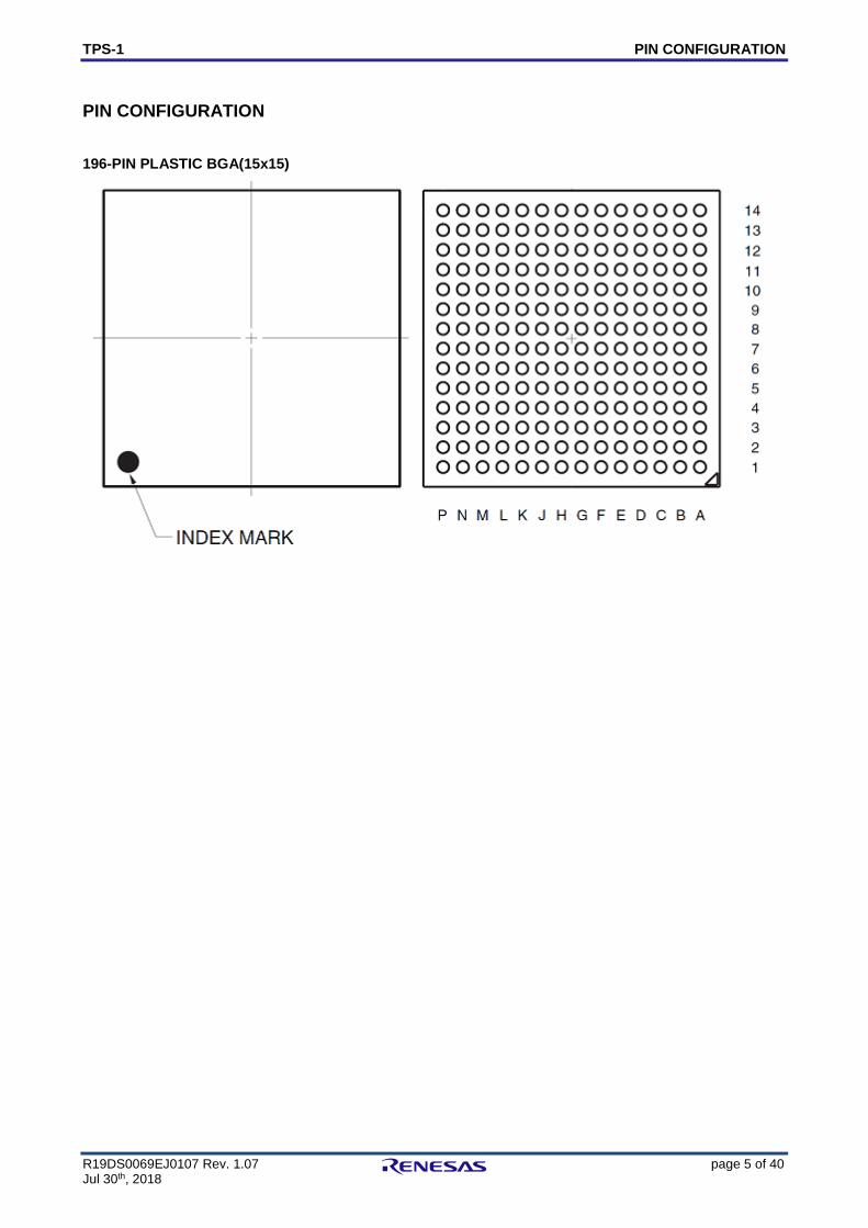
TPS-1 PIN CONFIGURATION
R19DS0069EJ0107 Rev. 1.07 page 5 of 40 Jul 30th, 2018
PIN CONFIGURATION 196-PIN PLASTIC BGA(15x15)
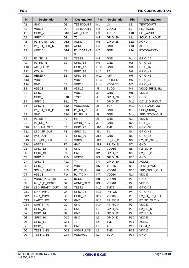
TPS-1 PIN CONFIGURATION
R19DS0069EJ0107 Rev. 1.07 page 6 of 40 Jul 30th, 2018
Pin Designation Pin Designation Pin Designation Pin Designation A1 GND D8 TESTDOUT5 H1 LX L8 TESTDOUT7 A2 VDD15 D9 TESTDOUT6 H2 VDD33 L9 PLL_AGND A3 GPIO_7 D10 ACT_PHY1 H3 TEST1 L10 PLL_AVDD A4 GPIO_4 D11 T6 H4 GPIO_26 L11 SCLK_2_INOUT A5 P1_FX_EN_OUT D12 AGND H5 GPIO_25 L12 AGND A6 P1_TD_OUT_N D13 AGND H6 GND L13 AGND A7 VDD15 D14 P1VDDARXT
X H7 GND L14 P2VDDARXTX
A8 P1_SD_N E1 TEST3 H8 GND M1 GPIO_36 A9 P1_RD_N E2 GPIO_16 H9 GND M2 GPIO_35 A10 ACT_PHY2 E3 GPIO_17 H10 GND M3 GPIO_37 A11 WD_IN E4 GPIO_18 H11 T2 M4 GPIO_42 A12 RESETN E5 GPIO_19 H12 ATP M5 GPIO_45 A13 VDD15 E6 VDD10 H13 EXTRES M6 GPIO_46 A14 GND E7 VDD10 H14 VDDACB M7 GPIO_47 B1 VDD33 E8 VDD10 J1 BVDD M8 VDDQ_PECL_B2 B2 GPIO_9 E9 VDD10 J2 GND M9 VDD15 B3 GPIO_8 E10 TMC1 J3 GPIO_28 M10 GND B4 GPIO_5 E11 T5 J4 GPIO_27 M11 I2C_2_D_INOUT B5 GPIO_1 E12 VDD33ESD J5 TCK M12 CS_FLASH_OUT B6 P1_TD_OUT_P E13 P1_RX_P J6 GND M13 SPI3_SRXD_IN B7 GND E14 P1_RX_N J7 GND M14 SPI3_STXD_OUT B8 P1_SD_P F1 FB J8 GND N1 VDD33 B9 P1_RD_P F2 AVDD_REG J9 GND N2 GPIO_40 B10 LED_MT_OUT F3 GPIO_22 J10 TM1 N3 GPIO_39 B11 LED_SF_OUT F4 GPIO_21 J11 T1 N4 GPIO_41 B12 WD_OUT F5 GPIO_20 J12 GND N5 GPIO_44 B13 LED_BF_OUT F6 VDD33 J13 P2_TX_P N6 P2_TD_OUT_P B14 VDD33 F7 GND J14 P2_TX_N N7 GND C1 GPIO_12 F8 GND K1 VDD15 N8 P2_SD_P C2 GPIO_13 F9 GND K2 GPIO_31 N9 P2_RD_P C3 GPIO_6 F10 VDD33 K3 GPIO_29 N10 GND C4 GPIO_3 F11 T4 K4 GPIO_30 N11 XCLK1 C5 GPIO_2 F12 VDD15 K5 TRSTN N12 TEST_SYNC C6 SCLK_1_INOUT F13 P1_TX_P K6 VDD10 N13 SPI3_SCLK_OUT C7 VDD33 F14 P1_TX_N K7 VDD10 N14 VDD33 C8 VDDQ_PECL_B1 G1 BGND K8 VDD10 P1 GND C9 I2C_1_D_INOUT G2 AGND_REG K9 VDD10 P2 VDD15 C10 LED_READY_OUT G3 TEST2 K10 TMC2 P3 GPIO_38 C11 LINK_PHY2 G4 GPIO_24 K11 INT_OUT P4 GPIO_43 C12 LINK_PHY1 G5 GPIO_23 K12 VDD15 P5 P2_FX_EN_OUT C13 UART6_RX G6 GND K13 P2_RX_P P6 P2_TD_OUT_N C14 UART6_TX G7 GND K14 P2_RX_N P7 VDD33 D1 GPIO_15 G8 GND L1 GPIO_34 P8 P2_SD_N D2 GPIO_14 G9 GND L2 GPIO_32 P9 P2_RD_N D3 GPIO_10 G10 GND L3 GPIO_33 P10 VDD33 D4 GPIO_11 G11 T3 L4 TM0 P11 XCLK2 D5 GPIO_0 G12 GND L5 TDI P12 BOOT_1 D6 TEST_1_IN G13 VSSAPLLCB L6 TMS P13 VDD15 D7 TEST_2_IN G14 VDDAPLL L7 TDO P14 GND
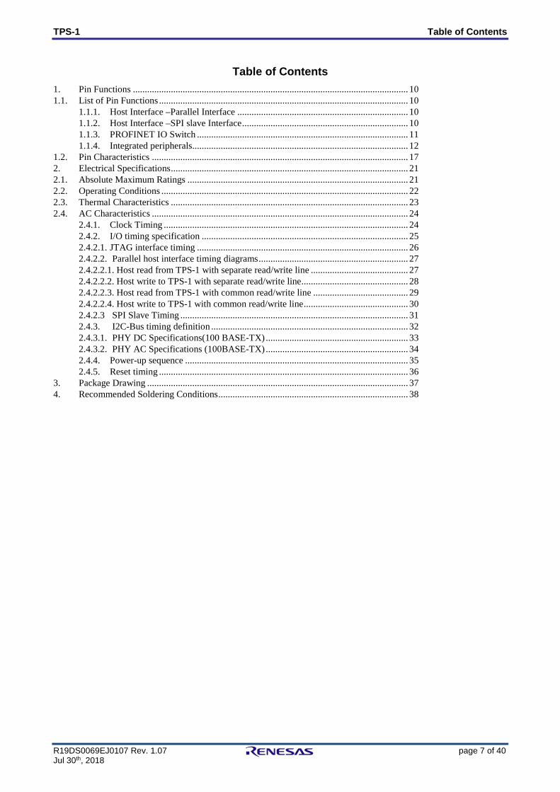
TPS-1 Table of Contents
R19DS0069EJ0107 Rev. 1.07 page 7 of 40 Jul 30th, 2018
Table of Contents
1. Pin Functions .................................................................................................................... 10 1.1. List of Pin Functions ......................................................................................................... 10
1.1.1. Host Interface –Parallel Interface ........................................................................ 10 1.1.2. Host Interface –SPI slave Interface ...................................................................... 10 1.1.3. PROFINET IO Switch ......................................................................................... 11 1.1.4. Integrated peripherals........................................................................................... 12
1.2. Pin Characteristics ............................................................................................................ 17 2. Electrical Specifications .................................................................................................... 21 2.1. Absolute Maximum Ratings ............................................................................................. 21 2.2. Operating Conditions ........................................................................................................ 22 2.3. Thermal Characteristics .................................................................................................... 23 2.4. AC Characteristics ............................................................................................................ 24
2.4.1. Clock Timing ....................................................................................................... 24 2.4.2. I/O timing specification ....................................................................................... 25 2.4.2.1. JTAG interface timing ......................................................................................... 26 2.4.2.2. Parallel host interface timing diagrams ............................................................... 27 2.4.2.2.1. Host read from TPS-1 with separate read/write line ......................................... 27 2.4.2.2.2. Host write to TPS-1 with separate read/write line ............................................. 28 2.4.2.2.3. Host read from TPS-1 with common read/write line ........................................ 29 2.4.2.2.4. Host write to TPS-1 with common read/write line ............................................ 30 2.4.2.3 SPI Slave Timing ................................................................................................ 31 2.4.3. I2C-Bus timing definition ................................................................................... 32 2.4.3.1. PHY DC Specifications(100 BASE-TX) ............................................................ 33 2.4.3.2. PHY AC Specifications (100BASE-TX) ............................................................ 34 2.4.4. Power-up sequence .............................................................................................. 35 2.4.5. Reset timing ......................................................................................................... 36
3. Package Drawing .............................................................................................................. 37 4. Recommended Soldering Conditions ................................................................................ 38
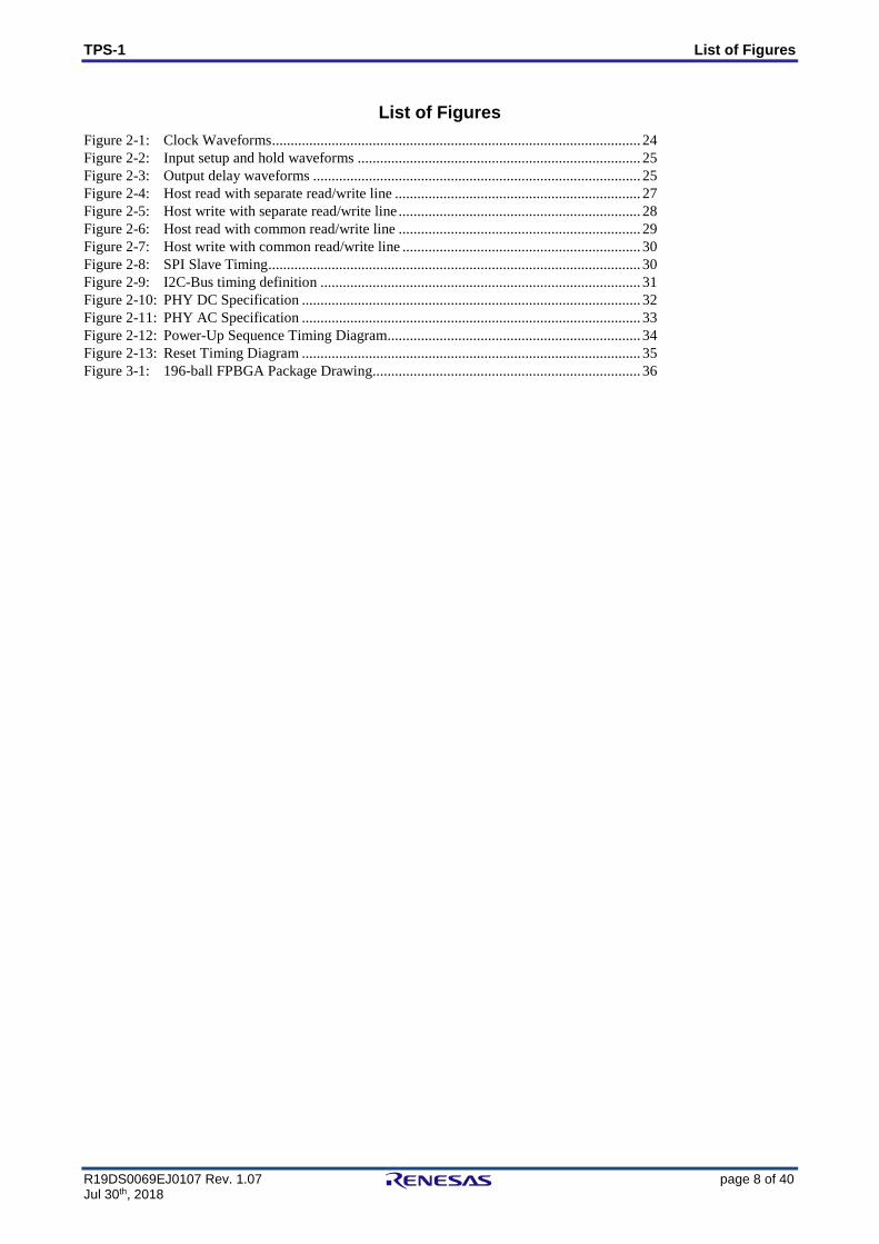
TPS-1 List of Figures
R19DS0069EJ0107 Rev. 1.07 page 8 of 40 Jul 30th, 2018
List of Figures Figure 2-1: Clock Waveforms ................................................................................................... 24 Figure 2-2: Input setup and hold waveforms ............................................................................ 25 Figure 2-3: Output delay waveforms ........................................................................................ 25 Figure 2-4: Host read with separate read/write line .................................................................. 27 Figure 2-5: Host write with separate read/write line ................................................................. 28 Figure 2-6: Host read with common read/write line ................................................................. 29 Figure 2-7: Host write with common read/write line ................................................................ 30 Figure 2-8: SPI Slave Timing .................................................................................................... 30 Figure 2-9: I2C-Bus timing definition ...................................................................................... 31 Figure 2-10: PHY DC Specification ........................................................................................... 32 Figure 2-11: PHY AC Specification ........................................................................................... 33 Figure 2-12: Power-Up Sequence Timing Diagram.................................................................... 34 Figure 2-13: Reset Timing Diagram ........................................................................................... 35 Figure 3-1: 196-ball FPBGA Package Drawing........................................................................ 36
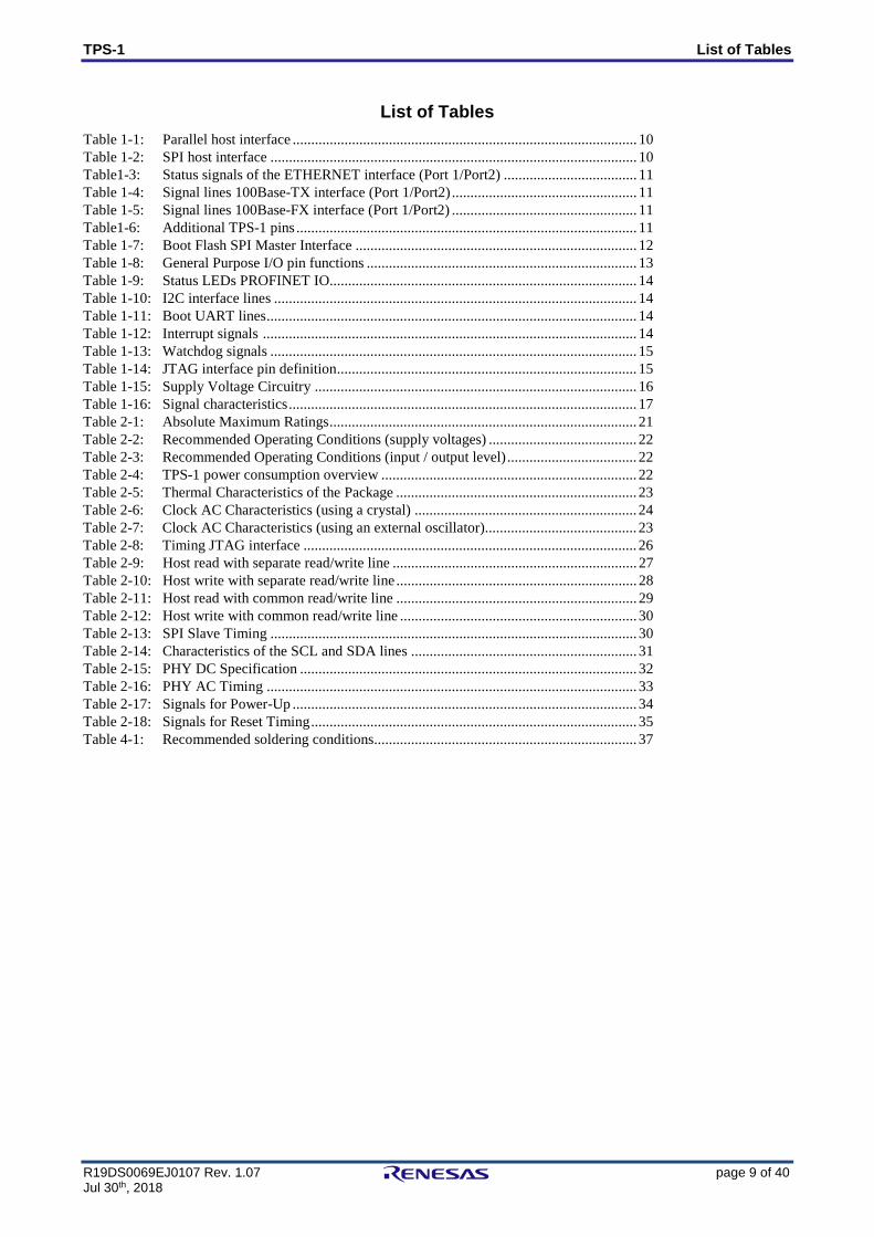
TPS-1 List of Tables
R19DS0069EJ0107 Rev. 1.07 page 9 of 40 Jul 30th, 2018
List of Tables Table 1-1: Parallel host interface ............................................................................................. 10 Table 1-2: SPI host interface ................................................................................................... 10 Table1-3: Status signals of the ETHERNET interface (Port 1/Port2) .................................... 11 Table 1-4: Signal lines 100Base-TX interface (Port 1/Port2) .................................................. 11 Table 1-5: Signal lines 100Base-FX interface (Port 1/Port2) .................................................. 11 Table1-6: Additional TPS-1 pins ............................................................................................ 11 Table 1-7: Boot Flash SPI Master Interface ............................................................................ 12 Table 1-8: General Purpose I/O pin functions ......................................................................... 13 Table 1-9: Status LEDs PROFINET IO................................................................................... 14 Table 1-10: I2C interface lines .................................................................................................. 14 Table 1-11: Boot UART lines .................................................................................................... 14 Table 1-12: Interrupt signals ..................................................................................................... 14 Table 1-13: Watchdog signals ................................................................................................... 15 Table 1-14: JTAG interface pin definition ................................................................................. 15 Table 1-15: Supply Voltage Circuitry ....................................................................................... 16 Table 1-16: Signal characteristics .............................................................................................. 17 Table 2-1: Absolute Maximum Ratings ................................................................................... 21 Table 2-2: Recommended Operating Conditions (supply voltages) ........................................ 22 Table 2-3: Recommended Operating Conditions (input / output level) ................................... 22 Table 2-4: TPS-1 power consumption overview ..................................................................... 22 Table 2-5: Thermal Characteristics of the Package ................................................................. 23 Table 2-6: Clock AC Characteristics (using a crystal) ............................................................ 24 Table 2-7: Clock AC Characteristics (using an external oscillator)......................................... 23 Table 2-8: Timing JTAG interface .......................................................................................... 26 Table 2-9: Host read with separate read/write line .................................................................. 27 Table 2-10: Host write with separate read/write line ................................................................. 28 Table 2-11: Host read with common read/write line ................................................................. 29 Table 2-12: Host write with common read/write line ................................................................ 30 Table 2-13: SPI Slave Timing ................................................................................................... 30 Table 2-14: Characteristics of the SCL and SDA lines ............................................................. 31 Table 2-15: PHY DC Specification ........................................................................................... 32 Table 2-16: PHY AC Timing .................................................................................................... 33 Table 2-17: Signals for Power-Up ............................................................................................. 34 Table 2-18: Signals for Reset Timing ........................................................................................ 35 Table 4-1: Recommended soldering conditions....................................................................... 37
TPS-1 1. Pin Functions
R19DS0069EJ0107 Rev. 1.07 page 10 of 40 Jul 30th, 2018
1. Pin Functions 1.1. List of Pin Functions
1.1.1. Host Interface –Parallel Interface
Table 1-1: Parallel host interface
Pin Name I/O Function Remarks Alternate Function LBU_WR_EN_IN I Write Control Active low (Intel mode) GPIO_0
0:write; 1:read (Motorola mode)
LBU_READ_EN_IN I Read Control Active low (Intel mode) GPIO_1 No function (Motorola mode)
LBU_CS_IN I Chip Select GPIO_2 LBU_BE_1_IN I Byte Select 1 GPIO_3 LBU_BE_2_IN I Byte Select 2 GPIO_4 LBU_READY_OUT O Ready Signal Polarity configurable GPIO_5 LBU_DATA(15:0) I/O data line 0 – 15 GPIO_(21:6) LBU_A(13:0)_IN I Address lines 0 - 13 GPIO_(35:22) LBU_SEG0_IN I Low Bit of the segment
select Page selection GPIO_36
LBU_SEG1_IN I High Bit of the segment select
Page selection GPIO_37
1.1.2. Host Interface –SPI slave Interface Table 1-2: SPI host interface
Pin Name I/O Function Remarks Alternate Function HOST_RESET_IN I Serial Reset The SPI Slave interface can be
reset by using this signal. (signal is active high)
GPIO_38
HOST_SFRN_IN I Serial Frame The start of a new SPI transfer is signaled.
GPIO_39
HOST_SRXD_IN I Serial Data Input MOSI (Master out Slave in) GPIO_40 HOST_SCLK_IN I Serial Clock Input Serial Clock driven by the SPI
Master GPIO_41
HOST_STXD_OUT O Serial Data Output MISO (Master in Slave out) GPIO_42 HOST_SHDR_OUT O Serial Header
Information header information available GPIO_43
TPS-1 1. Pin Functions
R19DS0069EJ0107 Rev. 1.07 page 11 of 40 Jul 30th, 2018
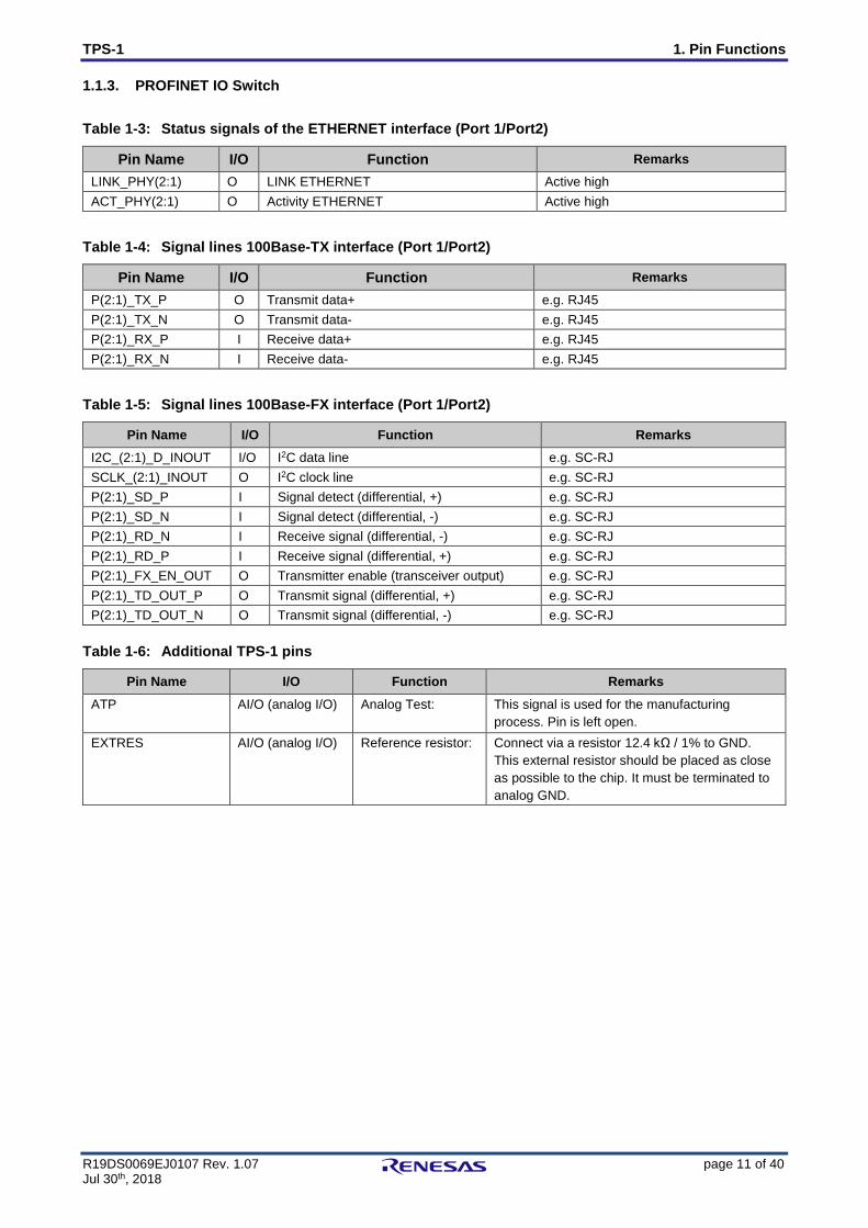
1.1.3. PROFINET IO Switch Table 1-3: Status signals of the ETHERNET interface (Port 1/Port2)
Pin Name I/O Function Remarks LINK_PHY(2:1) O LINK ETHERNET Active high ACT_PHY(2:1) O Activity ETHERNET Active high
Table 1-4: Signal lines 100Base-TX interface (Port 1/Port2)
Pin Name I/O Function Remarks P(2:1)_TX_P O Transmit data+ e.g. RJ45 P(2:1)_TX_N O Transmit data- e.g. RJ45 P(2:1)_RX_P I Receive data+ e.g. RJ45 P(2:1)_RX_N I Receive data- e.g. RJ45
Table 1-5: Signal lines 100Base-FX interface (Port 1/Port2)
Pin Name I/O Function Remarks I2C_(2:1)_D_INOUT I/O I2C data line e.g. SC-RJ SCLK_(2:1)_INOUT O I2C clock line e.g. SC-RJ P(2:1)_SD_P I Signal detect (differential, +) e.g. SC-RJ P(2:1)_SD_N I Signal detect (differential, -) e.g. SC-RJ P(2:1)_RD_N I Receive signal (differential, -) e.g. SC-RJ P(2:1)_RD_P I Receive signal (differential, +) e.g. SC-RJ P(2:1)_FX_EN_OUT O Transmitter enable (transceiver output) e.g. SC-RJ P(2:1)_TD_OUT_P O Transmit signal (differential, +) e.g. SC-RJ P(2:1)_TD_OUT_N O Transmit signal (differential, -) e.g. SC-RJ
Table 1-6: Additional TPS-1 pins
Pin Name I/O Function Remarks ATP AI/O (analog I/O) Analog Test:
This signal is used for the manufacturing process. Pin is left open.
EXTRES AI/O (analog I/O) Reference resistor:
Connect via a resistor 12.4 kΩ / 1% to GND. This external resistor should be placed as close as possible to the chip. It must be terminated to analog GND.
TPS-1 1. Pin Functions
R19DS0069EJ0107 Rev. 1.07 page 12 of 40 Jul 30th, 2018
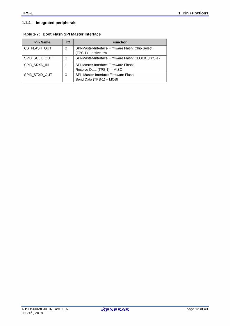
1.1.4. Integrated peripherals Table 1-7: Boot Flash SPI Master Interface
Pin Name I/O Function CS_FLASH_OUT O SPI-Master-Interface Firmware Flash: Chip Select
(TPS-1) – active low SPI3_SCLK_OUT O SPI-Master-Interface Firmware Flash: CLOCK (TPS-1)
SPI3_SRXD_IN I SPI-Master-Interface Firmware Flash: Receive Data (TPS-1) – MISO
SPI3_STXD_OUT O SPI- Master-Interface Firmware Flash: Send Data (TPS-1) – MOSI
TPS-1 1. Pin Functions
R19DS0069EJ0107 Rev. 1.07 page 13 of 40 Jul 30th, 2018
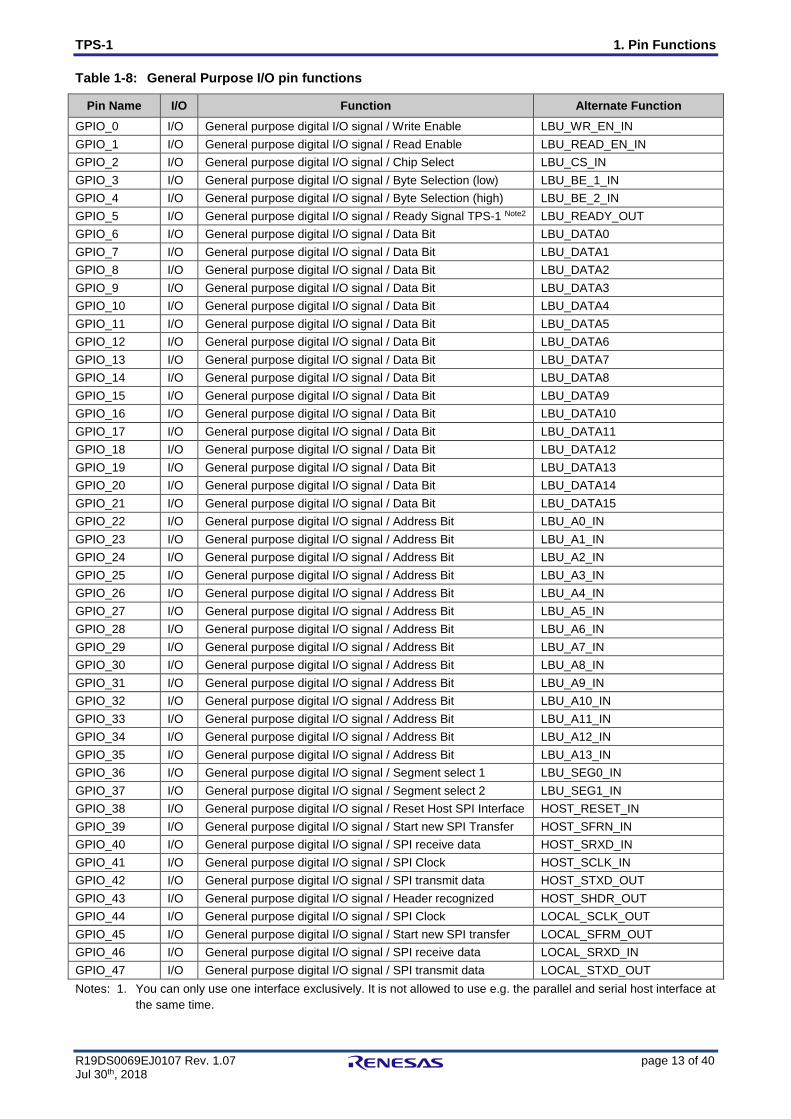
Table 1-8: General Purpose I/O pin functions
Pin Name I/O Function Alternate Function GPIO_0 I/O General purpose digital I/O signal / Write Enable LBU_WR_EN_IN GPIO_1 I/O General purpose digital I/O signal / Read Enable LBU_READ_EN_IN GPIO_2 I/O General purpose digital I/O signal / Chip Select LBU_CS_IN GPIO_3 I/O General purpose digital I/O signal / Byte Selection (low) LBU_BE_1_IN GPIO_4 I/O General purpose digital I/O signal / Byte Selection (high) LBU_BE_2_IN GPIO_5 I/O General purpose digital I/O signal / Ready Signal TPS-1 Note2 LBU_READY_OUT GPIO_6 I/O General purpose digital I/O signal / Data Bit LBU_DATA0 GPIO_7 I/O General purpose digital I/O signal / Data Bit LBU_DATA1 GPIO_8 I/O General purpose digital I/O signal / Data Bit LBU_DATA2 GPIO_9 I/O General purpose digital I/O signal / Data Bit LBU_DATA3 GPIO_10 I/O General purpose digital I/O signal / Data Bit LBU_DATA4 GPIO_11 I/O General purpose digital I/O signal / Data Bit LBU_DATA5 GPIO_12 I/O General purpose digital I/O signal / Data Bit LBU_DATA6 GPIO_13 I/O General purpose digital I/O signal / Data Bit LBU_DATA7 GPIO_14 I/O General purpose digital I/O signal / Data Bit LBU_DATA8 GPIO_15 I/O General purpose digital I/O signal / Data Bit LBU_DATA9 GPIO_16 I/O General purpose digital I/O signal / Data Bit LBU_DATA10 GPIO_17 I/O General purpose digital I/O signal / Data Bit LBU_DATA11 GPIO_18 I/O General purpose digital I/O signal / Data Bit LBU_DATA12 GPIO_19 I/O General purpose digital I/O signal / Data Bit LBU_DATA13 GPIO_20 I/O General purpose digital I/O signal / Data Bit LBU_DATA14 GPIO_21 I/O General purpose digital I/O signal / Data Bit LBU_DATA15 GPIO_22 I/O General purpose digital I/O signal / Address Bit LBU_A0_IN GPIO_23 I/O General purpose digital I/O signal / Address Bit LBU_A1_IN GPIO_24 I/O General purpose digital I/O signal / Address Bit LBU_A2_IN GPIO_25 I/O General purpose digital I/O signal / Address Bit LBU_A3_IN GPIO_26 I/O General purpose digital I/O signal / Address Bit LBU_A4_IN GPIO_27 I/O General purpose digital I/O signal / Address Bit LBU_A5_IN GPIO_28 I/O General purpose digital I/O signal / Address Bit LBU_A6_IN GPIO_29 I/O General purpose digital I/O signal / Address Bit LBU_A7_IN GPIO_30 I/O General purpose digital I/O signal / Address Bit LBU_A8_IN GPIO_31 I/O General purpose digital I/O signal / Address Bit LBU_A9_IN GPIO_32 I/O General purpose digital I/O signal / Address Bit LBU_A10_IN GPIO_33 I/O General purpose digital I/O signal / Address Bit LBU_A11_IN GPIO_34 I/O General purpose digital I/O signal / Address Bit LBU_A12_IN GPIO_35 I/O General purpose digital I/O signal / Address Bit LBU_A13_IN GPIO_36 I/O General purpose digital I/O signal / Segment select 1 LBU_SEG0_IN GPIO_37 I/O General purpose digital I/O signal / Segment select 2 LBU_SEG1_IN GPIO_38 I/O General purpose digital I/O signal / Reset Host SPI Interface HOST_RESET_IN GPIO_39 I/O General purpose digital I/O signal / Start new SPI Transfer HOST_SFRN_IN GPIO_40 I/O General purpose digital I/O signal / SPI receive data HOST_SRXD_IN GPIO_41 I/O General purpose digital I/O signal / SPI Clock HOST_SCLK_IN GPIO_42 I/O General purpose digital I/O signal / SPI transmit data HOST_STXD_OUT GPIO_43 I/O General purpose digital I/O signal / Header recognized HOST_SHDR_OUT GPIO_44 I/O General purpose digital I/O signal / SPI Clock LOCAL_SCLK_OUT GPIO_45 I/O General purpose digital I/O signal / Start new SPI transfer LOCAL_SFRM_OUT GPIO_46 I/O General purpose digital I/O signal / SPI receive data LOCAL_SRXD_IN GPIO_47 I/O General purpose digital I/O signal / SPI transmit data LOCAL_STXD_OUT Notes: 1. You can only use one interface exclusively. It is not allowed to use e.g. the parallel and serial host interface at
the same time.
TPS-1 1. Pin Functions
R19DS0069EJ0107 Rev. 1.07 page 14 of 40 Jul 30th, 2018
Notes: 2 The signal “LBU_READY_OUT” is designed to connect only to a single microcontroller. If you want to connect additional devices, you must add circuitry to realize the high-impedance state.
3. If the CPU does not have a READY input for connection to LBU_READY_OUT, customers can choose a wait time of 260 ns during each transfer cycle.
4. As soon as the signal HOST_SFRN_IN is set to “1”, no more data is received on the RxD interface. Setting the signal is not allowed during an ongoing transfer.
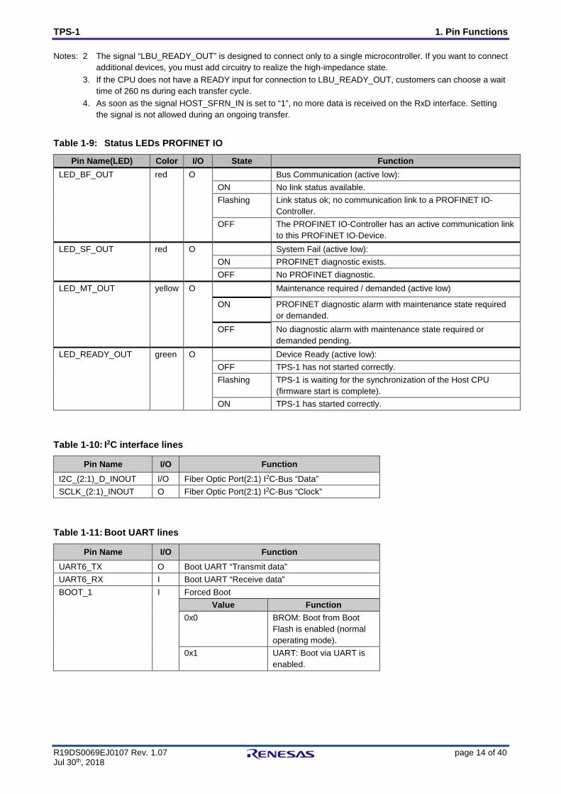
Table 1-9: Status LEDs PROFINET IO
Pin Name(LED) Color I/O State Function LED_BF_OUT red O Bus Communication (active low):
ON No link status available. Flashing Link status ok; no communication link to a PROFINET IO-
Controller. OFF The PROFINET IO-Controller has an active communication link
to this PROFINET IO-Device. LED_SF_OUT red O System Fail (active low):
ON PROFINET diagnostic exists. OFF No PROFINET diagnostic.
LED_MT_OUT yellow O Maintenance required / demanded (active low)
ON PROFINET diagnostic alarm with maintenance state required or demanded.
OFF No diagnostic alarm with maintenance state required or demanded pending.
LED_READY_OUT green O Device Ready (active low): OFF TPS-1 has not started correctly. Flashing TPS-1 is waiting for the synchronization of the Host CPU
(firmware start is complete). ON TPS-1 has started correctly.
Table 1-10: I2C interface lines
Pin Name I/O Function I2C_(2:1)_D_INOUT I/O Fiber Optic Port(2:1) I2C-Bus “Data” SCLK_(2:1)_INOUT O Fiber Optic Port(2:1) I2C-Bus “Clock”
Table 1-11: Boot UART lines
Pin Name I/O Function UART6_TX O Boot UART “Transmit data” UART6_RX I Boot UART “Receive data” BOOT_1 I Forced Boot
Value Function 0x0 BROM: Boot from Boot
Flash is enabled (normal operating mode).
0x1 UART: Boot via UART is enabled.
TPS-1 1. Pin Functions
R19DS0069EJ0107 Rev. 1.07 page 15 of 40 Jul 30th, 2018
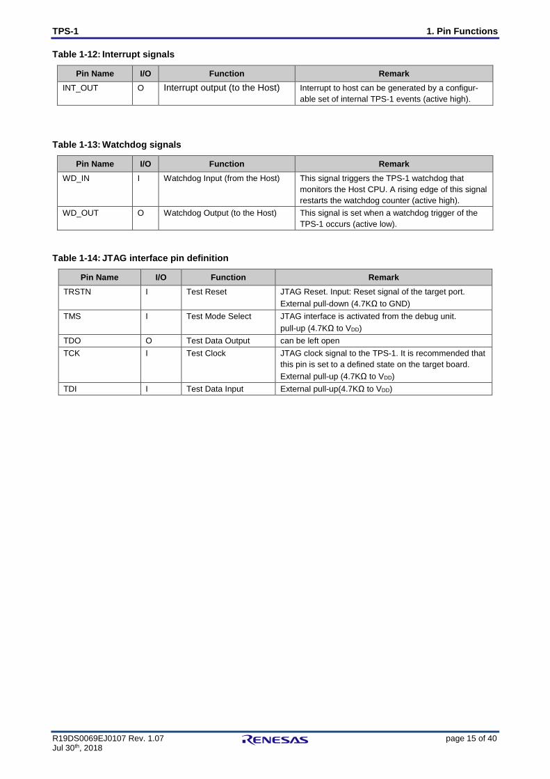
Table 1-12: Interrupt signals
Pin Name I/O Function Remark INT_OUT O Interrupt output (to the Host) Interrupt to host can be generated by a configur-
able set of internal TPS-1 events (active high).
Table 1-13: Watchdog signals
Pin Name I/O Function Remark WD_IN I Watchdog Input (from the Host) This signal triggers the TPS-1 watchdog that
monitors the Host CPU. A rising edge of this signal restarts the watchdog counter (active high).
WD_OUT O Watchdog Output (to the Host) This signal is set when a watchdog trigger of the TPS-1 occurs (active low).
Table 1-14: JTAG interface pin definition
Pin Name I/O Function Remark TRSTN I Test Reset JTAG Reset. Input: Reset signal of the target port.
External pull-down (4.7KΩ to GND) TMS I Test Mode Select JTAG interface is activated from the debug unit.
pull-up (4.7KΩ to VDD) TDO O Test Data Output can be left open TCK I Test Clock JTAG clock signal to the TPS-1. It is recommended that
this pin is set to a defined state on the target board. External pull-up (4.7KΩ to VDD)
TDI I Test Data Input External pull-up(4.7KΩ to VDD)
TPS-1 1. Pin Functions
R19DS0069EJ0107 Rev. 1.07 page 16 of 40 Jul 30th, 2018
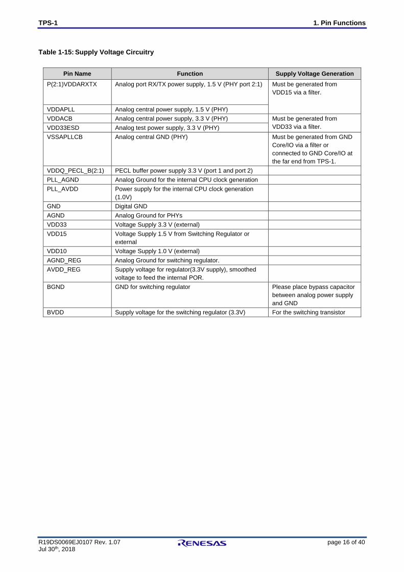
Table 1-15: Supply Voltage Circuitry
Pin Name Function Supply Voltage Generation P(2:1)VDDARXTX Analog port RX/TX power supply, 1.5 V (PHY port 2:1) Must be generated from
VDD15 via a filter.
VDDAPLL Analog central power supply, 1.5 V (PHY) VDDACB Analog central power supply, 3.3 V (PHY) Must be generated from
VDD33 via a filter. VDD33ESD Analog test power supply, 3.3 V (PHY) VSSAPLLCB Analog central GND (PHY) Must be generated from GND
Core/IO via a filter or connected to GND Core/IO at the far end from TPS-1.
VDDQ_PECL_B(2:1) PECL buffer power supply 3.3 V (port 1 and port 2) PLL_AGND Analog Ground for the internal CPU clock generation PLL_AVDD Power supply for the internal CPU clock generation
(1.0V)
GND Digital GND AGND Analog Ground for PHYs VDD33 Voltage Supply 3.3 V (external) VDD15 Voltage Supply 1.5 V from Switching Regulator or
external
VDD10 Voltage Supply 1.0 V (external) AGND_REG Analog Ground for switching regulator. AVDD_REG Supply voltage for regulator(3.3V supply), smoothed
voltage to feed the internal POR.
BGND GND for switching regulator Please place bypass capacitor between analog power supply and GND
BVDD Supply voltage for the switching regulator (3.3V) For the switching transistor
TPS-1 1. Pin Functions
R19DS0069EJ0107 Rev. 1.07 page 17 of 40 Jul 30th, 2018
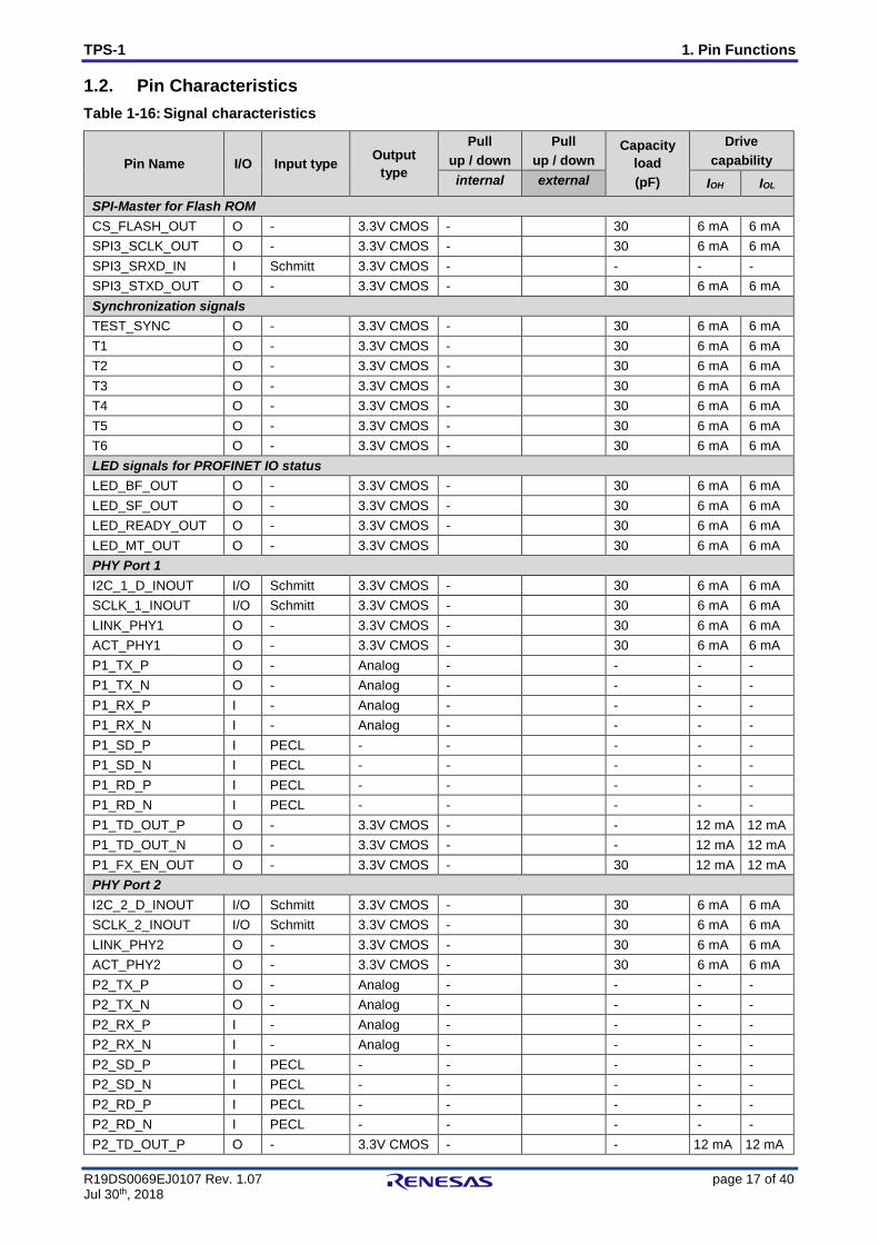
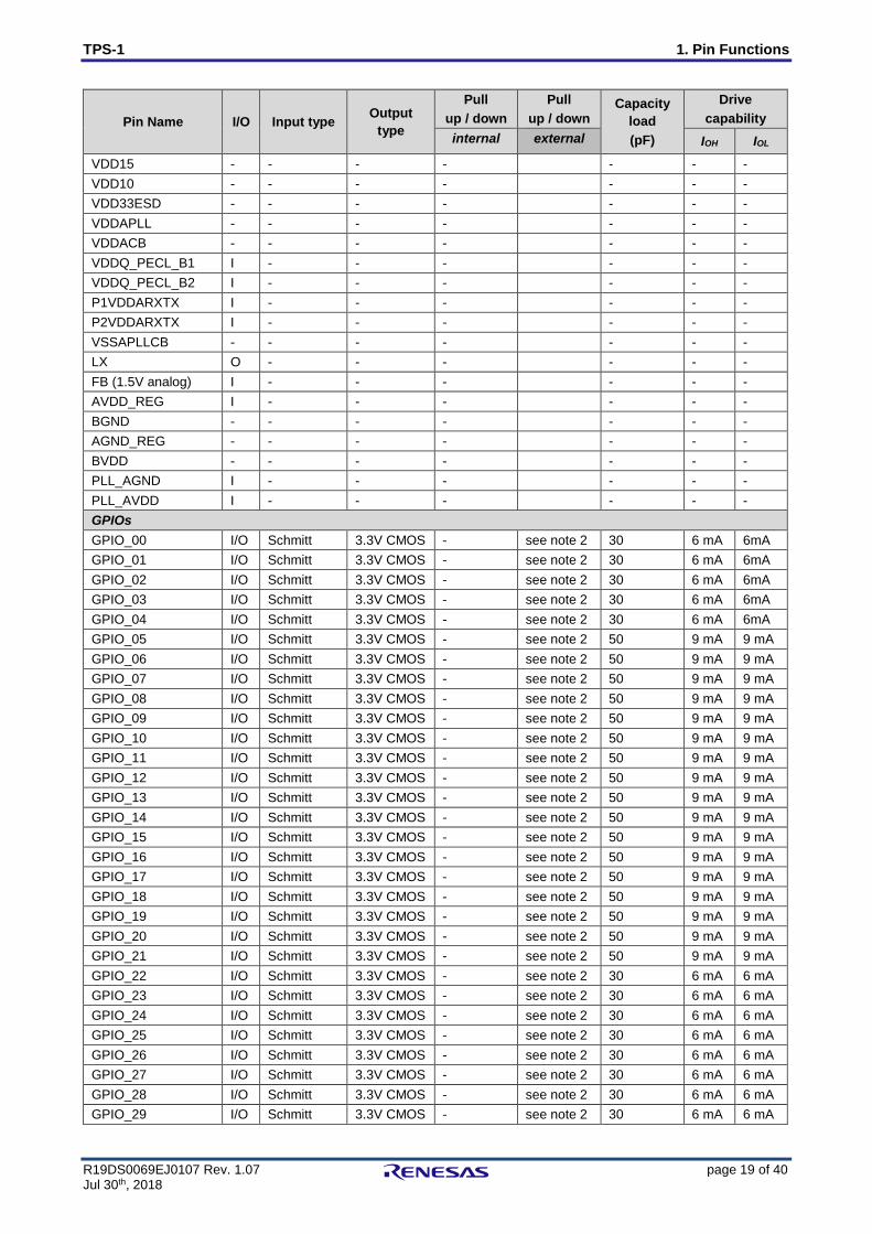
1.2. Pin Characteristics Table 1-16: Signal characteristics
Pin Name I/O Input type Output type
Pull up / down
Pull up / down
Capacity load (pF)
Drive capability
internal external IOH IOL SPI-Master for Flash ROM CS_FLASH_OUT O - 3.3V CMOS - 30 6 mA 6 mA SPI3_SCLK_OUT O - 3.3V CMOS - 30 6 mA 6 mA SPI3_SRXD_IN I Schmitt 3.3V CMOS - - - - SPI3_STXD_OUT O - 3.3V CMOS - 30 6 mA 6 mA Synchronization signals TEST_SYNC O - 3.3V CMOS - 30 6 mA 6 mA T1 O - 3.3V CMOS - 30 6 mA 6 mA T2 O - 3.3V CMOS - 30 6 mA 6 mA T3 O - 3.3V CMOS - 30 6 mA 6 mA T4 O - 3.3V CMOS - 30 6 mA 6 mA T5 O - 3.3V CMOS - 30 6 mA 6 mA T6 O - 3.3V CMOS - 30 6 mA 6 mA LED signals for PROFINET IO status LED_BF_OUT O - 3.3V CMOS - 30 6 mA 6 mA LED_SF_OUT O - 3.3V CMOS - 30 6 mA 6 mA LED_READY_OUT O - 3.3V CMOS - 30 6 mA 6 mA LED_MT_OUT O - 3.3V CMOS 30 6 mA 6 mA PHY Port 1 I2C_1_D_INOUT I/O Schmitt 3.3V CMOS - 30 6 mA 6 mA SCLK_1_INOUT I/O Schmitt 3.3V CMOS - 30 6 mA 6 mA LINK_PHY1 O - 3.3V CMOS - 30 6 mA 6 mA ACT_PHY1 O - 3.3V CMOS - 30 6 mA 6 mA P1_TX_P O - Analog - - - - P1_TX_N O - Analog - - - - P1_RX_P I - Analog - - - - P1_RX_N I - Analog - - - - P1_SD_P I PECL - - - - - P1_SD_N I PECL - - - - - P1_RD_P I PECL - - - - - P1_RD_N I PECL - - - - - P1_TD_OUT_P O - 3.3V CMOS - - 12 mA 12 mA P1_TD_OUT_N O - 3.3V CMOS - - 12 mA 12 mA P1_FX_EN_OUT O - 3.3V CMOS - 30 12 mA 12 mA PHY Port 2 I2C_2_D_INOUT I/O Schmitt 3.3V CMOS - 30 6 mA 6 mA SCLK_2_INOUT I/O Schmitt 3.3V CMOS - 30 6 mA 6 mA LINK_PHY2 O - 3.3V CMOS - 30 6 mA 6 mA ACT_PHY2 O - 3.3V CMOS - 30 6 mA 6 mA P2_TX_P O - Analog - - - - P2_TX_N O - Analog - - - - P2_RX_P I - Analog - - - - P2_RX_N I - Analog - - - - P2_SD_P I PECL - - - - - P2_SD_N I PECL - - - - - P2_RD_P I PECL - - - - - P2_RD_N I PECL - - - - - P2_TD_OUT_P O - 3.3V CMOS - - 12 mA 12 mA
TPS-1 1. Pin Functions
R19DS0069EJ0107 Rev. 1.07 page 18 of 40 Jul 30th, 2018
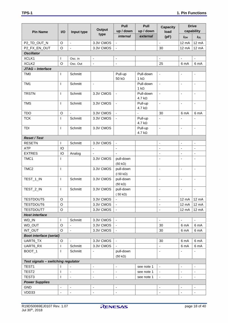
Pin Name I/O Input type Output type
Pull up / down
Pull up / down
Capacity load (pF)
Drive capability
internal external IOH IOL P2_TD_OUT_N O - 3.3V CMOS - - 12 mA 12 mA P2_FX_EN_OUT O - 3.3V CMOS - 30 12 mA 12 mA Oscillator XCLK1 I Osc. in - - - - - XCLK2 O Osc. Out - - 25 6 mA 6 mA JTAG – Interface TM0 I Schmitt Pull-up
50 kΩ Pull-down 1 kΩ
- - -
TM1 I Schmitt - Pull-down 1 kΩ
- - -
TRSTN I Schmitt 3.3V CMOS - Pull-down 4.7 kΩ
- - -
TMS I Schmitt 3.3V CMOS - Pull-up 4.7 kΩ
- - -
TDO O - 3.3V CMOS - - 30 6 mA 6 mA TCK I Schmitt 3.3V CMOS - Pull-up
4.7 kΩ - - -
TDI I Schmitt 3.3V CMOS Pull-up 4.7 kΩ
- - -
Reset / Test RESETN I Schmitt 3.3V CMOS - - - - ATP IO - - - - - EXTRES IO Analog - - - - - TMC1 I 3.3V CMOS pull-down
(50 kΩ) - - -
TMC2 I 3.3V CMOS pull-down (l 50 kΩ)
- - -
TEST_1_IN I Schmitt 3.3V CMOS pull-down (50 kΩ)
- - -
TEST_2_IN I Schmitt 3.3V CMOS pull-down ( 50 kΩ)
- - -
TESTDOUT5 O 3.3V CMOS - - 12 mA 12 mA TESTDOUT6 O 3.3V CMOS - - 12 mA 12 mA TESTDOUT7 O 3.3V CMOS - - 12 mA 12 mA Host interface WD_IN I Schmitt 3.3V CMOS - - - - WD_OUT O - 3.3V CMOS - 30 6 mA 6 mA INT_OUT O - 3.3V CMOS - 30 6 mA 6 mA Boot interface (serial) UART6_TX O - 3.3V CMOS - 30 6 mA 6 mA UART6_RX I Schmitt 3.3V CMOS - - 6 mA 6 mA BOOT_1 I Schmitt - pull-down
(50 kΩ) - - -
Test signals – switching regulator TEST1 I - - - see note 1 - - - TEST2 I - - - see note 1 - - - TEST3 I - - - see note 1 - - - Power Supplies GND - - - - - - - VDD33 - - - - - - -
TPS-1 1. Pin Functions
R19DS0069EJ0107 Rev. 1.07 page 19 of 40 Jul 30th, 2018
Pin Name I/O Input type Output type
Pull up / down
Pull up / down
Capacity load (pF)
Drive capability
internal external IOH IOL VDD15 - - - - - - - VDD10 - - - - - - - VDD33ESD - - - - - - - VDDAPLL - - - - - - - VDDACB - - - - - - - VDDQ_PECL_B1 I - - - - - - VDDQ_PECL_B2 I - - - - - - P1VDDARXTX I - - - - - - P2VDDARXTX I - - - - - - VSSAPLLCB - - - - - - - LX O - - - - - - FB (1.5V analog) I - - - - - - AVDD_REG I - - - - - - BGND - - - - - - - AGND_REG - - - - - - - BVDD - - - - - - - PLL_AGND I - - - - - - PLL_AVDD I - - - - - - GPIOs GPIO_00 I/O Schmitt 3.3V CMOS - see note 2 30 6 mA 6mA GPIO_01 I/O Schmitt 3.3V CMOS - see note 2 30 6 mA 6mA GPIO_02 I/O Schmitt 3.3V CMOS - see note 2 30 6 mA 6mA GPIO_03 I/O Schmitt 3.3V CMOS - see note 2 30 6 mA 6mA GPIO_04 I/O Schmitt 3.3V CMOS - see note 2 30 6 mA 6mA GPIO_05 I/O Schmitt 3.3V CMOS - see note 2 50 9 mA 9 mA GPIO_06 I/O Schmitt 3.3V CMOS - see note 2 50 9 mA 9 mA GPIO_07 I/O Schmitt 3.3V CMOS - see note 2 50 9 mA 9 mA GPIO_08 I/O Schmitt 3.3V CMOS - see note 2 50 9 mA 9 mA GPIO_09 I/O Schmitt 3.3V CMOS - see note 2 50 9 mA 9 mA GPIO_10 I/O Schmitt 3.3V CMOS - see note 2 50 9 mA 9 mA GPIO_11 I/O Schmitt 3.3V CMOS - see note 2 50 9 mA 9 mA GPIO_12 I/O Schmitt 3.3V CMOS - see note 2 50 9 mA 9 mA GPIO_13 I/O Schmitt 3.3V CMOS - see note 2 50 9 mA 9 mA GPIO_14 I/O Schmitt 3.3V CMOS - see note 2 50 9 mA 9 mA GPIO_15 I/O Schmitt 3.3V CMOS - see note 2 50 9 mA 9 mA GPIO_16 I/O Schmitt 3.3V CMOS - see note 2 50 9 mA 9 mA GPIO_17 I/O Schmitt 3.3V CMOS - see note 2 50 9 mA 9 mA GPIO_18 I/O Schmitt 3.3V CMOS - see note 2 50 9 mA 9 mA GPIO_19 I/O Schmitt 3.3V CMOS - see note 2 50 9 mA 9 mA GPIO_20 I/O Schmitt 3.3V CMOS - see note 2 50 9 mA 9 mA GPIO_21 I/O Schmitt 3.3V CMOS - see note 2 50 9 mA 9 mA GPIO_22 I/O Schmitt 3.3V CMOS - see note 2 30 6 mA 6 mA GPIO_23 I/O Schmitt 3.3V CMOS - see note 2 30 6 mA 6 mA GPIO_24 I/O Schmitt 3.3V CMOS - see note 2 30 6 mA 6 mA GPIO_25 I/O Schmitt 3.3V CMOS - see note 2 30 6 mA 6 mA GPIO_26 I/O Schmitt 3.3V CMOS - see note 2 30 6 mA 6 mA GPIO_27 I/O Schmitt 3.3V CMOS - see note 2 30 6 mA 6 mA GPIO_28 I/O Schmitt 3.3V CMOS - see note 2 30 6 mA 6 mA GPIO_29 I/O Schmitt 3.3V CMOS - see note 2 30 6 mA 6 mA
TPS-1 1. Pin Functions
R19DS0069EJ0107 Rev. 1.07 page 20 of 40 Jul 30th, 2018
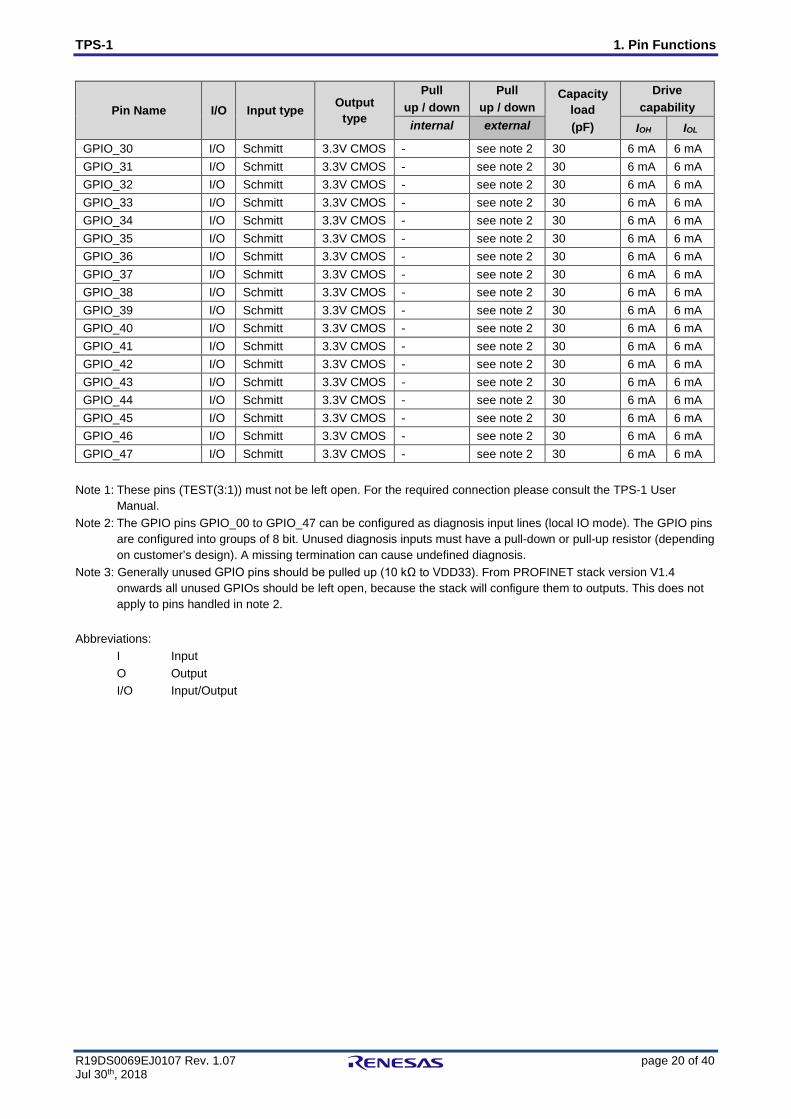
Pin Name I/O Input type Output type
Pull up / down
Pull up / down
Capacity load (pF)
Drive capability
internal external IOH IOL GPIO_30 I/O Schmitt 3.3V CMOS - see note 2 30 6 mA 6 mA GPIO_31 I/O Schmitt 3.3V CMOS - see note 2 30 6 mA 6 mA GPIO_32 I/O Schmitt 3.3V CMOS - see note 2 30 6 mA 6 mA GPIO_33 I/O Schmitt 3.3V CMOS - see note 2 30 6 mA 6 mA GPIO_34 I/O Schmitt 3.3V CMOS - see note 2 30 6 mA 6 mA GPIO_35 I/O Schmitt 3.3V CMOS - see note 2 30 6 mA 6 mA GPIO_36 I/O Schmitt 3.3V CMOS - see note 2 30 6 mA 6 mA GPIO_37 I/O Schmitt 3.3V CMOS - see note 2 30 6 mA 6 mA GPIO_38 I/O Schmitt 3.3V CMOS - see note 2 30 6 mA 6 mA GPIO_39 I/O Schmitt 3.3V CMOS - see note 2 30 6 mA 6 mA GPIO_40 I/O Schmitt 3.3V CMOS - see note 2 30 6 mA 6 mA GPIO_41 I/O Schmitt 3.3V CMOS - see note 2 30 6 mA 6 mA GPIO_42 I/O Schmitt 3.3V CMOS - see note 2 30 6 mA 6 mA GPIO_43 I/O Schmitt 3.3V CMOS - see note 2 30 6 mA 6 mA GPIO_44 I/O Schmitt 3.3V CMOS - see note 2 30 6 mA 6 mA GPIO_45 I/O Schmitt 3.3V CMOS - see note 2 30 6 mA 6 mA GPIO_46 I/O Schmitt 3.3V CMOS - see note 2 30 6 mA 6 mA GPIO_47 I/O Schmitt 3.3V CMOS - see note 2 30 6 mA 6 mA
Note 1: These pins (TEST(3:1)) must not be left open. For the required connection please consult the TPS-1 User
Manual. Note 2: The GPIO pins GPIO_00 to GPIO_47 can be configured as diagnosis input lines (local IO mode). The GPIO pins
are configured into groups of 8 bit. Unused diagnosis inputs must have a pull-down or pull-up resistor (depending on customer’s design). A missing termination can cause undefined diagnosis.
Note 3: Generally unused GPIO pins should be pulled up (10 kΩ to VDD33). From PROFINET stack version V1.4 onwards all unused GPIOs should be left open, because the stack will configure them to outputs. This does not apply to pins handled in note 2.
Abbreviations:
I Input O Output I/O Input/Output
TPS-1 2. Electrical Specifications
R19DS0069EJ0107 Rev. 1.07 page 21 of 40 Jul 30th, 2018
2. Electrical Specifications
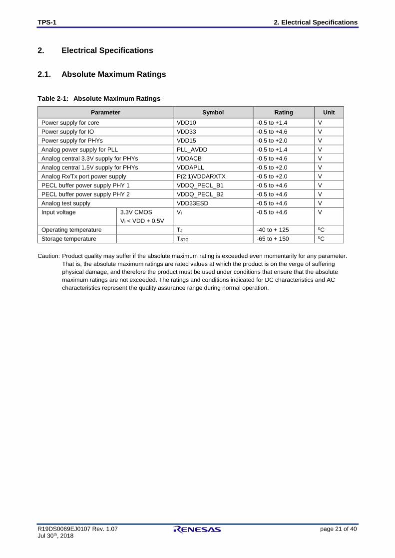
2.1. Absolute Maximum Ratings
Table 2-1: Absolute Maximum Ratings
Parameter Symbol Rating Unit Power supply for core VDD10 -0.5 to +1.4 V Power supply for IO VDD33 -0.5 to +4.6 V Power supply for PHYs VDD15 -0.5 to +2.0 V Analog power supply for PLL PLL_AVDD -0.5 to +1.4 V Analog central 3.3V supply for PHYs VDDACB -0.5 to +4.6 V Analog central 1.5V supply for PHYs VDDAPLL -0.5 to +2.0 V Analog Rx/Tx port power supply P(2:1)VDDARXTX -0.5 to +2.0 V PECL buffer power supply PHY 1 VDDQ_PECL_B1 -0.5 to +4.6 V PECL buffer power supply PHY 2 VDDQ_PECL_B2 -0.5 to +4.6 V Analog test supply VDD33ESD -0.5 to +4.6 V Input voltage 3.3V CMOS
VI < VDD + 0.5V VI -0.5 to +4.6 V
Operating temperature TJ -40 to + 125 0C Storage temperature TSTG -65 to + 150 0C
Caution: Product quality may suffer if the absolute maximum rating is exceeded even momentarily for any parameter.
That is, the absolute maximum ratings are rated values at which the product is on the verge of suffering physical damage, and therefore the product must be used under conditions that ensure that the absolute maximum ratings are not exceeded. The ratings and conditions indicated for DC characteristics and AC characteristics represent the quality assurance range during normal operation.
TPS-1 2. Electrical Specifications
R19DS0069EJ0107 Rev. 1.07 page 22 of 40 Jul 30th, 2018
2.2. Operating Conditions
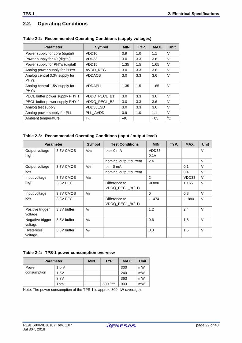
Table 2-2: Recommended Operating Conditions (supply voltages)
Parameter Symbol MIN. TYP. MAX. Unit Power supply for core (digital) VDD10 0.9 1.0 1.1 V Power supply for IO (digital) VDD33 3.0 3.3 3.6 V Power supply for PHYs (digital) VDD15 1.35 1.5 1.65 V Analog power supply for PHYs AVDD_REG 3.0 3.3 3.6 V Analog central 3.3V supply for PHYs
VDDACB 3.0 3.3 3.6 V
Analog central 1.5V supply for PHYs
VDDAPLL 1.35 1.5 1.65 V
PECL buffer power supply PHY 1 VDDQ_PECL_B1 3.0 3.3 3.6 V PECL buffer power supply PHY 2 VDDQ_PECL_B2 3.0 3.3 3.6 V Analog test supply VDD33ESD 3.0 3.3 3.6 V Analog power supply for PLL PLL_AVDD 0.9 1.0 1.1 V Ambient temperature TA -40 +85 0C
Table 2-3: Recommended Operating Conditions (input / output level)
Parameter Symbol Test Conditions MIN. TYP. MAX. Unit Output voltage high
3.3V CMOS VOH IOH= 0 mA VDD33 – 0.1V
V
nominal output current 2.4 V Output voltage low
3.3V CMOS VOL IOL= 0 mA 0.1 V nominal output current 0.4 V
Input voltage high
3.3V CMOS VIH 2 VDD33 V 3.3V PECL Difference to
VDDQ_PECL_B(2:1) -0.880 1.165 V
Input voltage low
3.3V CMOS VIL 0 0.8 V 3.3V PECL Difference to
VDDQ_PECL_B(2:1) -1.474 -1.880 V
Positive trigger voltage
3.3V buffer VP 1.2 2.4 V
Negative trigger voltage
3.3V buffer VN 0.6 1.8 V
Hysteresis voltage
3.3V buffer VH 0.3 1.5 V
Table 2-4: TPS-1 power consumption overview
Parameter MIN. TYP. MAX. Unit Power consumption
1.0 V 300 mW 1.5V 240 mW 3.3V 363 mW Total: 800 Note 903 mW
Note: The power consumption of the TPS-1 is approx. 800mW (average).
TPS-1 2. Electrical Specifications
R19DS0069EJ0107 Rev. 1.07 page 23 of 40 Jul 30th, 2018
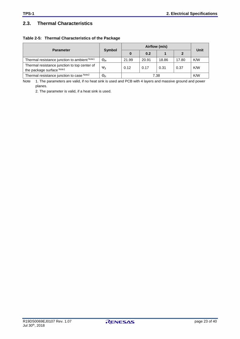
2.3. Thermal Characteristics
Table 2-5: Thermal Characteristics of the Package
Parameter Symbol Airflow (m/s)
Unit 0 0.2 1 2
Thermal resistance junction to ambient Note1 Θja 21.99 20.91 18.86 17.80 K/W Thermal resistance junction to top center of the package surface Note1 Ψjt 0.12 0.17 0.31 0.37 K/W
Thermal resistance junction to case Note2 Θjc 7.38 K/W Note 1. The parameters are valid, if no heat sink is used and PCB with 4 layers and massive ground and power
planes. 2. The parameter is valid, if a heat sink is used.
TPS-1 2. Electrical Specifications
R19DS0069EJ0107 Rev. 1.07 page 24 of 40 Jul 30th, 2018
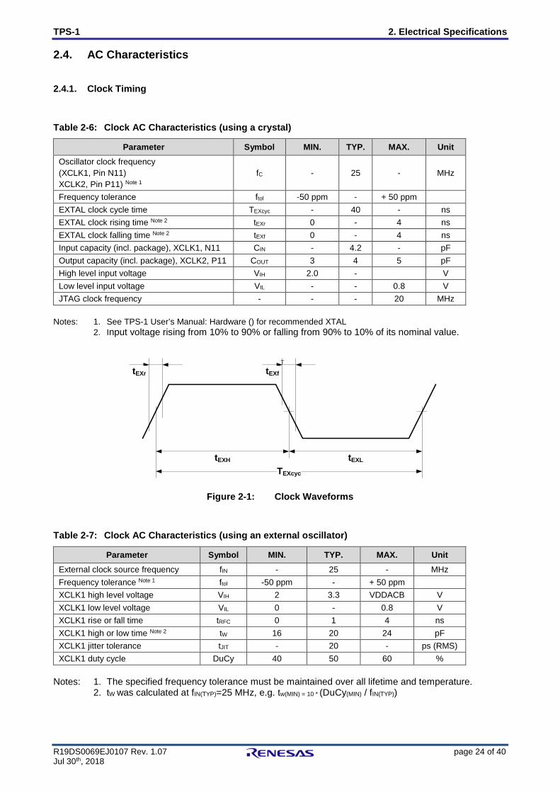
2.4. AC Characteristics
2.4.1. Clock Timing Table 2-6: Clock AC Characteristics (using a crystal)
Parameter Symbol MIN. TYP. MAX. Unit Oscillator clock frequency (XCLK1, Pin N11) XCLK2, Pin P11) Note 1
fC - 25 - MHz
Frequency tolerance ftol -50 ppm - + 50 ppm EXTAL clock cycle time TEXcyc - 40 - ns EXTAL clock rising time Note 2 tEXr 0 - 4 ns EXTAL clock falling time Note 2 tEXf 0 - 4 ns Input capacity (incl. package), XCLK1, N11 CIN - 4.2 - pF Output capacity (incl. package), XCLK2, P11 COUT 3 4 5 pF High level input voltage VIH 2.0 - V Low level input voltage VIL - - 0.8 V JTAG clock frequency - - - 20 MHz
Notes: 1. See TPS-1 User’s Manual: Hardware () for recommended XTAL 2. Input voltage rising from 10% to 90% or falling from 90% to 10% of its nominal value.
TEXcyc
tEXr tEXf
tEXLtEXH
T
Figure 2-1: Clock Waveforms Table 2-7: Clock AC Characteristics (using an external oscillator)
Parameter Symbol MIN. TYP. MAX. Unit External clock source frequency fIN - 25 - MHz Frequency tolerance Note 1 ftol -50 ppm - + 50 ppm XCLK1 high level voltage VIH 2 3.3 VDDACB V XCLK1 low level voltage VIL 0 - 0.8 V XCLK1 rise or fall time tRFC 0 1 4 ns XCLK1 high or low time Note 2 tW 16 20 24 pF XCLK1 jitter tolerance tJIT - 20 - ps (RMS) XCLK1 duty cycle DuCy 40 50 60 %
Notes: 1. The specified frequency tolerance must be maintained over all lifetime and temperature. 2. tW was calculated at fIN(TYP)=25 MHz, e.g. tw(MIN) = 10 * (DuCy(MIN) / fIN(TYP))
TPS-1 2. Electrical Specifications
R19DS0069EJ0107 Rev. 1.07 page 25 of 40 Jul 30th, 2018
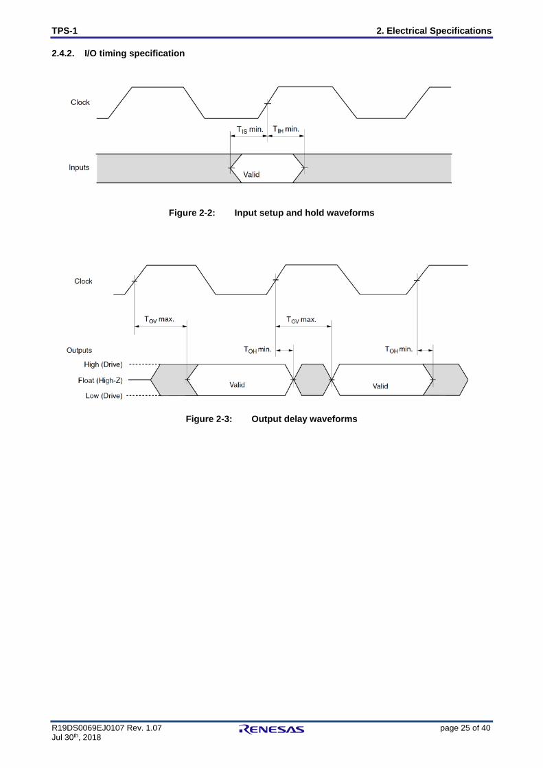
2.4.2. I/O timing specification
Figure 2-2: Input setup and hold waveforms
Figure 2-3: Output delay waveforms
TPS-1 2. Electrical Specifications
R19DS0069EJ0107 Rev. 1.07 page 26 of 40 Jul 30th, 2018
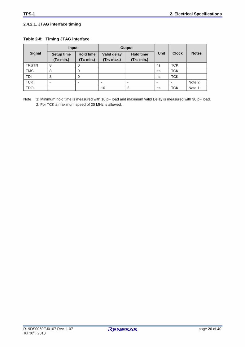
2.4.2.1. JTAG interface timing
Table 2-8: Timing JTAG interface
Signal Input Output
Unit Clock Notes Setup time (TIS min.)
Hold time (TIH min.)
Valid delay (TOV max.)
Hold time (TOH min.)
TRSTN 8 0 ns TCK TMS 8 0 ns TCK TDI 8 0 ns TCK TCK - - - - - - Note 2 TDO 10 2 ns TCK Note 1
Note 1: Minimum hold time is measured with 10 pF load and maximum valid Delay is measured with 30 pF load. 2: For TCK a maximum speed of 20 MHz is allowed.
TPS-1 2. Electrical Specifications
R19DS0069EJ0107 Rev. 1.07 page 27 of 40 Jul 30th, 2018
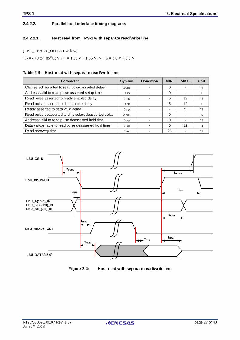
2.4.2.2. Parallel host interface timing diagrams
2.4.2.2.1. Host read from TPS-1 with separate read/write line
(LBU_READY_OUT active low)
TA = - 40 to +85OC; VDD15 = 1.35 V ~ 1.65 V; VDD33 = 3.0 V ~ 3.6 V
Table 2-9: Host read with separate read/write line
Parameter Symbol Condition MIN. MAX. Unit Chip select asserted to read pulse asserted delay tCSRS - 0 - ns Address valid to read pulse asserted setup time tARS - 0 - ns Read pulse asserted to ready enabled delay tRRE - 5 12 ns Read pulse asserted to data enable delay tRDE - 5 12 ns Ready asserted to data valid delay tRTD - - 5 ns Read pulse deasserted to chip select deasserted delay tRCSH - 0 - ns Address valid to read pulse deasserted hold time tRHA - 0 - ns Data valid/enable to read pulse deasserted hold time tRDH - 0 12 ns Read recovery time tRR - 25 - ns
LBU_A(13:0)_INLBU_SEG(1:0)_INLBU_BE_(2:1)_IN
LBU_READY_OUT
LBU_DATA(15:0)
LBU_CS_N
LBU_RD_EN_N
tCSRS
tARS
tRRE
tRDEtRTD
tRDH
tRAH
tRR
tRCSH
Figure 2-4: Host read with separate read/write line
TPS-1 2. Electrical Specifications
R19DS0069EJ0107 Rev. 1.07 page 28 of 40 Jul 30th, 2018
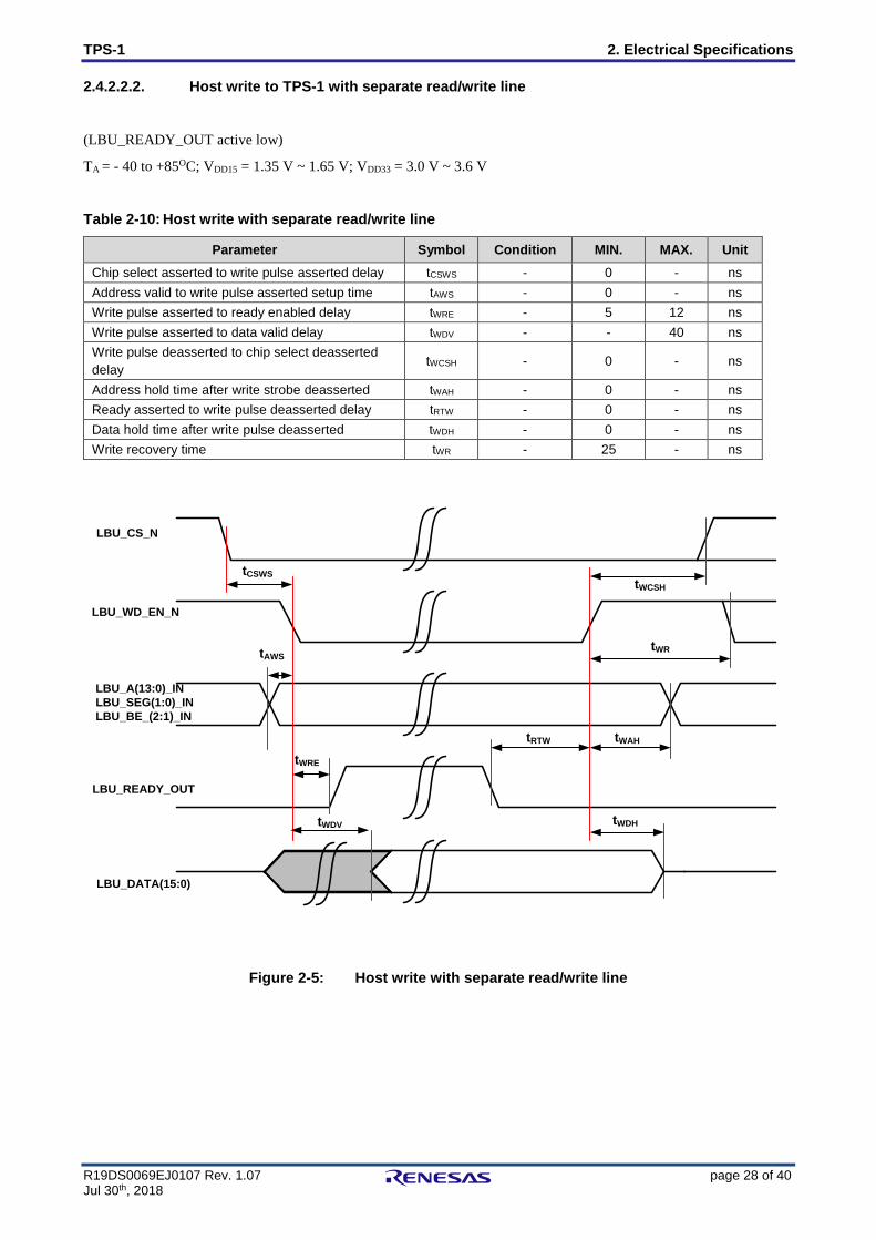
2.4.2.2.2. Host write to TPS-1 with separate read/write line
(LBU_READY_OUT active low)
TA = - 40 to +85OC; VDD15 = 1.35 V ~ 1.65 V; VDD33 = 3.0 V ~ 3.6 V
Table 2-10: Host write with separate read/write line
Parameter Symbol Condition MIN. MAX. Unit Chip select asserted to write pulse asserted delay tCSWS - 0 - ns Address valid to write pulse asserted setup time tAWS - 0 - ns Write pulse asserted to ready enabled delay tWRE - 5 12 ns Write pulse asserted to data valid delay tWDV - - 40 ns Write pulse deasserted to chip select deasserted delay tWCSH - 0 - ns
Address hold time after write strobe deasserted tWAH - 0 - ns Ready asserted to write pulse deasserted delay tRTW - 0 - ns Data hold time after write pulse deasserted tWDH - 0 - ns Write recovery time tWR - 25 - ns
LBU_A(13:0)_INLBU_SEG(1:0)_INLBU_BE_(2:1)_IN
LBU_READY_OUT
LBU_DATA(15:0)
LBU_CS_N
LBU_WD_EN_N
tCSWS
tAWS
tWRE
tWDV tWDH
tWAH
tWR
tWCSH
tRTW
Figure 2-5: Host write with separate read/write line
TPS-1 2. Electrical Specifications
R19DS0069EJ0107 Rev. 1.07 page 29 of 40 Jul 30th, 2018
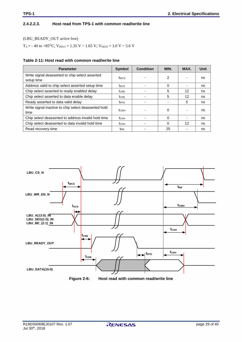
2.4.2.2.3. Host read from TPS-1 with common read/write line
(LBU_READY_OUT active low)
TA = - 40 to +85OC; VDD15 = 1.35 V ~ 1.65 V; VDD33 = 3.0 V ~ 3.6 V
Table 2-11: Host read with common read/write line
Parameter Symbol Condition MIN. MAX. Unit Write signal deasserted to chip select asserted setup time tWCS - 2 - ns
Address valid to chip select asserted setup time tACS - 0 - ns Chip select asserted to ready enabled delay tCRE - 5 12 ns Chip select asserted to data enable delay tCDE - 5 12 ns Ready asserted to data valid delay tRTD - - 5 ns Write signal inactive to chip select deasserted hold time tCWH - 0 - ns
Chip select deasserted to address invalid hold time tCAH - 0 - ns Chip select deasserted to data invalid hold time tCDH - 0 12 ns Read recovery time tRR - 25 - ns
Figure 2-6: Host read with common read/write line
LBU_A(13:0)_INLBU_SEG(1:0)_INLBU_BE_(2:1)_IN
LBU_READY_OUT
LBU_DATA(15:0)
LBU_CS_N
LBU_WR_EN_N
tWCS
tACS
tCRE
tCDEtRTD
tCDH
tCAH
tRR
tCWH
TPS-1 2. Electrical Specifications
R19DS0069EJ0107 Rev. 1.07 page 30 of 40 Jul 30th, 2018
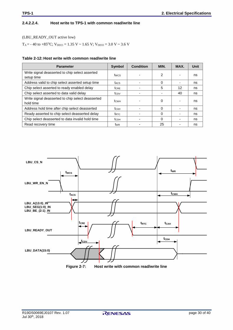
2.4.2.2.4. Host write to TPS-1 with common read/write line
(LBU_READY_OUT active low)
TA = - 40 to +85OC; VDD15 = 1.35 V ~ 1.65 V; VDD33 = 3.0 V ~ 3.6 V
Table 2-12: Host write with common read/write line
Parameter Symbol Condition MIN. MAX. Unit Write signal deasserted to chip select asserted setup time tWCS - 2 - ns
Address valid to chip select asserted setup time tACS - 0 - ns Chip select asserted to ready enabled delay tCRE - 5 12 ns Chip select asserted to data valid delay tCDV - - 40 ns Write signal deasserted to chip select deasserted hold time tCWH - 0 - ns
Address hold time after chip select deasserted tCAH - 0 - ns Ready asserted to chip select deasserted delay tRTC - 0 - ns Chip select deasserted to data invalid hold time tCDH - 0 - ns Read recovery time tWR - 25 - ns
Figure 2-7: Host write with common read/write line
LBU_A(13:0)_INLBU_SEG(1:0)_INLBU_BE_(2:1)_IN
LBU_READY_OUT
LBU_DATA(15:0)
LBU_CS_N
LBU_WR_EN_N
tWCS
tACS
tCRE
tCDV
tRTC
tCDH
tCAH
tWR
tCWH
TPS-1 2. Electrical Specifications
R19DS0069EJ0107 Rev. 1.07 page 31 of 40 Jul 30th, 2018
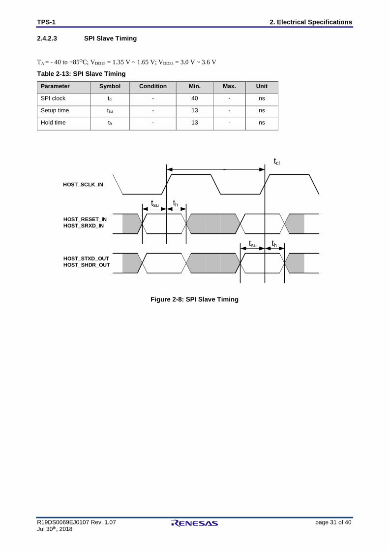
HOST_SCLK_IN
HOST_RESET_INHOST_SRXD_IN
HOST_STXD_OUTHOST_SHDR_OUT
tcl
tsu th
tsu th
2.4.2.3 SPI Slave Timing
TA = - 40 to +85OC; VDD15 = 1.35 V ~ 1.65 V; VDD33 = 3.0 V ~ 3.6 V
Table 2-13: SPI Slave Timing
Parameter Symbol Condition Min. Max. Unit
SPI clock tcl - 40 - ns
Setup time tsu - 13 - ns
Hold time th - 13 - ns
Figure 2-8: SPI Slave Timing
TPS-1 2. Electrical Specifications
R19DS0069EJ0107 Rev. 1.07 page 32 of 40 Jul 30th, 2018
2.4.3. I2C-Bus timing definition
TA = - 40 to +85OC; VDD15 = 1.35 V ~ 1.65 V; VDD33 = 3.0 V ~ 3.6 V
Table 2-14: Characteristics of the SCL and SDA lines
Parameter Symbol Standard-Mode Fast-Mode
Unit Min. Max. Min. Max.
SCL clock frequency fSCL 0 100 0 400 kHz Bus free time between a STOP and START condition tBUF 4.7 - 1.3 - µs
Hold time (repeated) Start condition. After this period, the first clock pulse is generated
tHD;STA 4.0 - 0.6 - µs
LOW period of the SCL clock tLOW 4.7 - 1.3 - µs HIGH period of the SCL clock tHIGH 4.0 - 0.6 - µs Set-up time for repeated START condition tSU;DAT 4.7 - 0.6 - µs
Data hold time tHD;DAT 0(1) - 0(1) 0.9 µs Data set-up time tSU;STA 250 - 100(2) - ns Rise time of both SDA and SCL signals tR - 1000 20+0.1Cb 300 ns Fall time of both SDA and SCL signals tf - 300 20+0.1Cb 300 ns Capacitive load for each bus line Cb - 400 - 400 pF
Notes: 1. The device must internally provide a hold time of at least 300 ns for the SDA signal in order to bridge the undefined region of the falling edge of SCL.
2. A fast-mode device can be used in a Standard-bus system, but the requirement tSU;STA must be met.
tBUF
tLOW
tHD;STA
tR
tHD;DATtHIGH
tF
tSU;DAT tSU;STA
tHD;STA
I2C_x_D_INOUT
SCLK_x_INOUT
Figure 2-9: I2C-Bus timing definition
TPS-1 2. Electrical Specifications
R19DS0069EJ0107 Rev. 1.07 page 33 of 40 Jul 30th, 2018
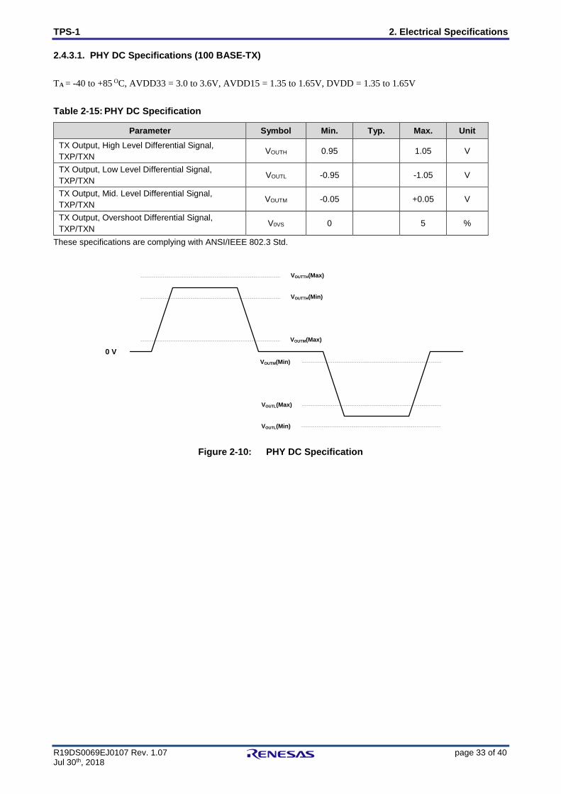
2.4.3.1. PHY DC Specifications (100 BASE-TX) TA = -40 to +85 OC, AVDD33 = 3.0 to 3.6V, AVDD15 = 1.35 to 1.65V, DVDD = 1.35 to 1.65V
Table 2-15: PHY DC Specification
Parameter Symbol Min. Typ. Max. Unit TX Output, High Level Differential Signal, TXP/TXN VOUTH 0.95 1.05 V
TX Output, Low Level Differential Signal, TXP/TXN VOUTL -0.95 -1.05 V
TX Output, Mid. Level Differential Signal, TXP/TXN VOUTM -0.05 +0.05 V
TX Output, Overshoot Differential Signal, TXP/TXN V0VS 0 5 %
These specifications are complying with ANSI/IEEE 802.3 Std.
0 V
VOUTTH(Max)
VOUTTH(Min)
VOUTM(Min)
VOUTM(Max)
VOUTL(Min)
VOUTL(Max)
Figure 2-10: PHY DC Specification
TPS-1 2. Electrical Specifications
R19DS0069EJ0107 Rev. 1.07 page 34 of 40 Jul 30th, 2018
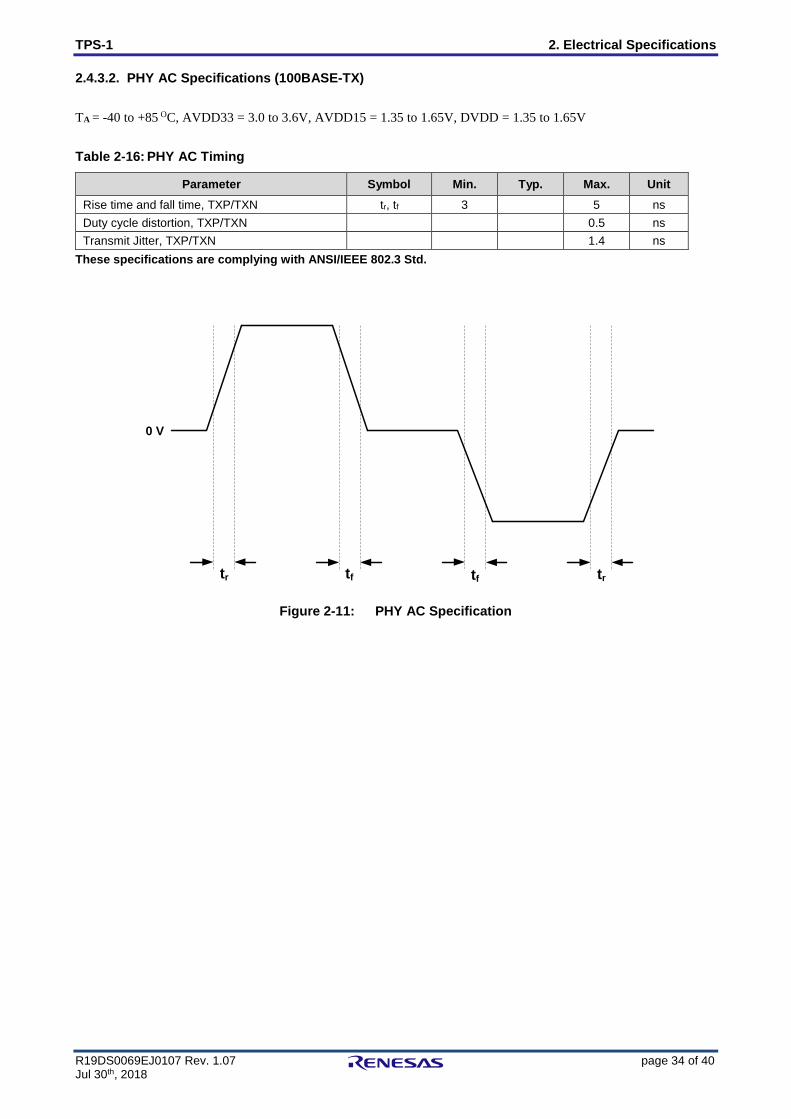
2.4.3.2. PHY AC Specifications (100BASE-TX) TA = -40 to +85 OC, AVDD33 = 3.0 to 3.6V, AVDD15 = 1.35 to 1.65V, DVDD = 1.35 to 1.65V
Table 2-16: PHY AC Timing
Parameter Symbol Min. Typ. Max. Unit Rise time and fall time, TXP/TXN tr, tf 3 5 ns Duty cycle distortion, TXP/TXN 0.5 ns Transmit Jitter, TXP/TXN 1.4 ns
These specifications are complying with ANSI/IEEE 802.3 Std.
0 V
tr trtftf
Figure 2-11: PHY AC Specification
TPS-1 2. Electrical Specifications
R19DS0069EJ0107 Rev. 1.07 page 35 of 40 Jul 30th, 2018
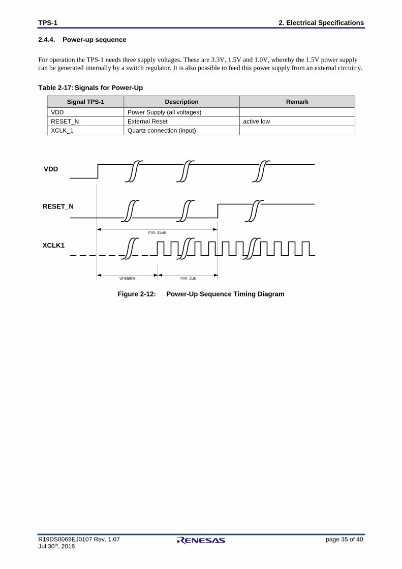
2.4.4. Power-up sequence For operation the TPS-1 needs three supply voltages. These are 3.3V, 1.5V and 1.0V, whereby the 1.5V power supply can be generated internally by a switch regulator. It is also possible to feed this power supply from an external circuitry.
Table 2-17: Signals for Power-Up
Signal TPS-1 Description Remark VDD Power Supply (all voltages) RESET_N External Reset active low XCLK_1 Quartz connection (input)
VDD
RESET_N
XCLK1
min. 35us
Unstable min. 2us
Figure 2-12: Power-Up Sequence Timing Diagram
TPS-1 2. Electrical Specifications
R19DS0069EJ0107 Rev. 1.07 page 36 of 40 Jul 30th, 2018
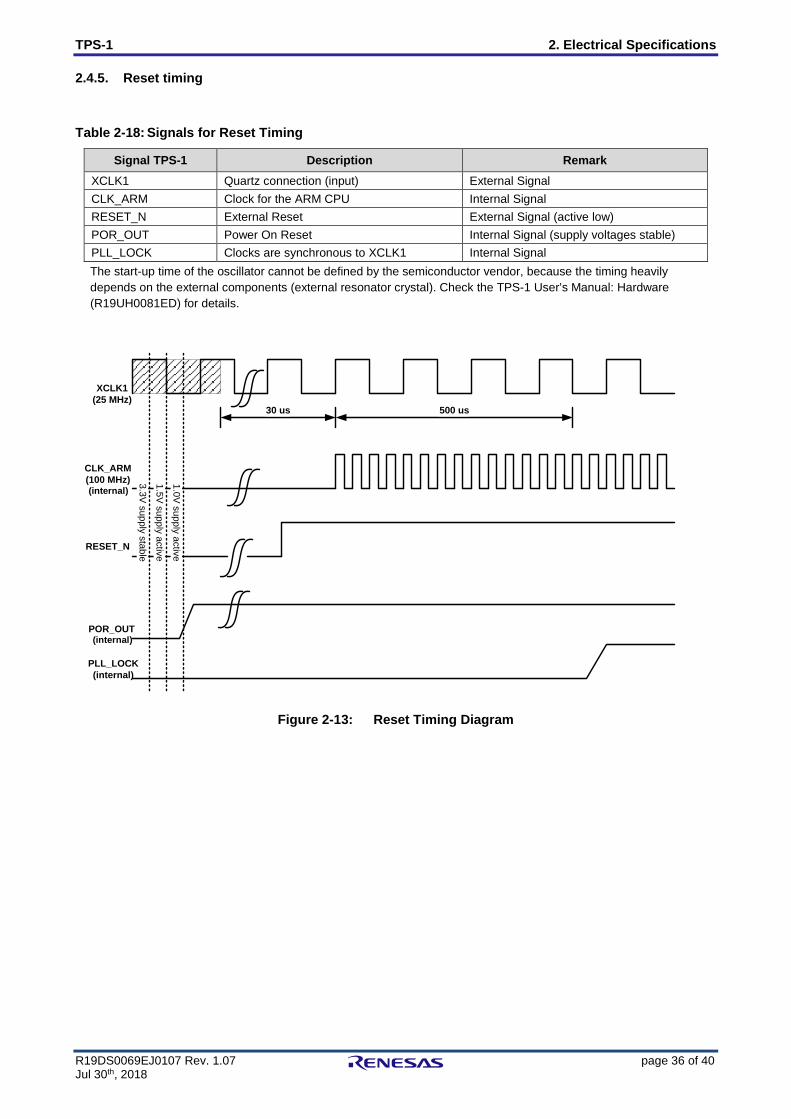
2.4.5. Reset timing Table 2-18: Signals for Reset Timing
Signal TPS-1 Description Remark XCLK1 Quartz connection (input) External Signal CLK_ARM Clock for the ARM CPU Internal Signal RESET_N External Reset External Signal (active low) POR_OUT Power On Reset Internal Signal (supply voltages stable) PLL_LOCK Clocks are synchronous to XCLK1 Internal Signal The start-up time of the oscillator cannot be defined by the semiconductor vendor, because the timing heavily depends on the external components (external resonator crystal). Check the TPS-1 User’s Manual: Hardware (R19UH0081ED) for details.
XCLK1(25 MHz)
RESET_N
CLK_ARM(100 MHz)
PLL_LOCK(internal)
3.3V supply stable
1.5V supply activePOR_OUT
30 us 500 us
1.0V supply active
Figure 2-13: Reset Timing Diagram
(internal)
(internal)
TPS-1 3. Package Drawing
R19DS0069EJ0107 Rev. 1.07 page 37 of 40 Jul 30th, 2018
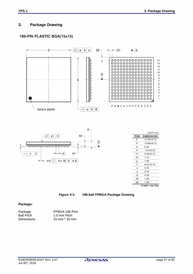
3. Package Drawing
Figure 3-1: 196-ball FPBGA Package Drawing Package: Package FPBGA 196 Pins Ball Pitch 1.0 mm Pitch Dimensions 15 mm * 15 mm
TPS-1 4. Recommended Soldering Conditions
R19DS0069EJ0107 Rev. 1.07 page 38 of 40 Jul 30th, 2018
4. Recommended Soldering Conditions Solder this product under the following recommended conditions.
For details of the recommended soldering conditions, refer to the information document.
Renesas Semiconductor Package Mount Manual, (Rev.5.0, Feb 2015) (R50ZZ0003EJ0500)
The applied standard is “IR60-107-3”. Table 4-1: Recommended soldering conditions
Condition Symbol Soldering Conditions IR60 Package peak temperature: 2600C, Time: 60 seconds max. (at 2200C or higher). -107 Exposure limit: 7 daysNote (after that, prebake at 1250C for 20 to 72 hours). -3 Count: Three times or less.
Note: After opening the dry pack, store it at 250C or less and 65% RH or less for the allowable storage period.
TPS-1
R19DS0069EJ0107 Rev. 1.07 page 39 of 40 Jul 30th, 2018
Instructions for the use of product In this section, the precautions are described for over whole of CMOS device. Please refer to this manual about individual precaution. When there is a mention unlike the text of this manual, a mention of the text takes first priority
1. Handling of Unused Pins
Handle unused pins in accord with the directions given under Handling of Unused Pins in the manual. - The input pins of CMOS products are generally in the high-impedance state. In operation with an unused pin in
the open-circuit state, extra electromagnetic noise is induced in the vicinity of LSI, associated shoot-through current flows internally, and malfunctions occur due to the false recognition of the pin state as an input signal become possible. Unused pins should be handled as described under Handling of Unused Pins in the manual.
2. Processing at Power-on
The state of the product is undefined at the moment when power is supplied. - The states of internal circuits in the LSI are indeterminate and the states of register settings and pins are
undefined at the moment when power is supplied. In a finished product where the reset signal is applied to the external reset pin, the states of pins are not guaranteed from the moment when power is supplied until the reset process is completed. In a similar way, the states of pins in a product that is reset by an on-chip power-on reset function are not guaranteed from the moment when power is supplied until the power reaches the level at which resetting has been specified.
3. Prohibition of Access to Reserved Addresses
Access to reserved addresses is prohibited. - The reserved addresses are provided for the possible future expansion of functions. Do not access these
addresses; the correct operation of LSI is not guaranteed if they are accessed. 4. Clock Signals
After applying a reset, only release the reset line after the operating clock signal has become stable. When switching the clock signal during program execution, wait until the target clock signal has stabilized. - When the clock signal is generated with an external resonator (or from an external oscillator) during a reset,
ensure that the reset line is only released after full stabilization of the clock signal. Moreover, when switching to a clock signal produced with an external resonator (or by an external oscillator) while program execution is in progress, wait until the target clock signal is stable.
TPS-1
R19DS0069EJ0107 Rev. 1.07 page 40 of 40 Jul 30th, 2018
Renesas Electronics America Inc. 2880 Scott Boulevard Santa Clara, CA 95050-2554, U.S.A. Tel: +1-408-588-6000, Fax: +1-408-588-6130 Renesas Electronics Canada Limited 1101 Nicholson Road, Newmarket, Ontario L3Y 9C3, Canada Tel: +1-905-898-5441, Fax: +1-905-898-3220 Renesas Electronics Europe Limited Dukes Meadow, Millboard Road, Bourne End, Buckinghamshire, SL8 5FH, U.K Tel: +44-1628-651-700, Fax: +44-1628-651-804 Renesas Electronics Europe GmbH Arcadiastrasse 10, 40472 Düsseldorf, Germany Tel: +49-211-65030, Fax: +49-211-6503-1327 Renesas Electronics (China) Co., Ltd. 7th Floor, Quantum Plaza, No.27 ZhiChunLu Haidian District, Beijing 100083, P.R.China Tel: +86-10-8235-1155, Fax: +86-10-8235-7679 Renesas Electronics (Shanghai) Co., Ltd. Unit 204, 205, AZIA Center, No.1233 Lujiazui Ring Rd., Pudong District, Shanghai 200120, China Tel: +86-21-5877-1818, Fax: +86-21-6887-7858 / -7898 Renesas Electronics Hong Kong Limited Unit 1601-1613, 16/F., Tower 2, Grand Century Place, 193 Prince Edward Road West, Mongkok, Kowloon, Hong Kong Tel: +852-2886-9318, Fax: +852 2886-9022/9044 Renesas Electronics Taiwan Co., Ltd. 13F, No. 363, Fu Shing North Road, Taipei, Taiwan Tel: +886-2-8175-9600, Fax: +886 2-8175-9670 Renesas Electronics Singapore Pte. Ltd. 80 Bendemeer Road, Unit #06-02 Hyflux Innovation Centre Singapore 339949 Tel: +65-6213-0200, Fax: +65-6213-0300 Renesas Electronics Malaysia Sdn.Bhd. Unit 906, Block B, Menara Amcorp, Amcorp Trade Centre, No. 18, Jln Persiaran Barat, 46050 Petaling Jaya, Selangor Darul Ehsan, Malaysia Tel: +60-3-7955-9390, Fax: +60-3-7955-9510 Renesas Electronics Korea Co., Ltd. 11F., Samik Lavied' or Bldg., 720-2 Yeoksam-Dong, Kangnam-Ku, Seoul 135-080, Korea Tel: +82-2-558-3737, Fax: +82-2-558-5141
© 2012-2015 Renesas Electronics Corporation. All rights reserved
Notice 1. Descriptions of circuits, software and other related information in this document are provided only to illustrate the operation of semiconductor products and application examples. You are
fully responsible for the incorporation of these circuits, software, and information in the design of your equipment. Renesas Electronics assumes no responsibility for any losses incurred by you or third parties arising from the use of these circuits, software, or information.
2. Renesas Electronics has used reasonable care in preparing the information included in this document, but Renesas Electronics does not warrant that such information is error free. Renesas Electronics assumes no liability whatsoever for any damages incurred by you resulting from errors in or omissions from the information included herein.
3. Renesas Electronics does not assume any liability for infringement of patents, copyrights, or other intellectual property rights of third parties by or arising from the use of Renesas Electronics products or technical information described in this document. No license, express, implied or otherwise, is granted hereby under any patents, copyrights or other intellectual property rights of Renesas Electronics or others.
4. You should not alter, modify, copy, or otherwise misappropriate any Renesas Electronics product, whether in whole or in part. Renesas Electronics assumes no responsibility for any losses incurred by you or third parties arising from such alteration, modification, copy or otherwise misappropriation of Renesas Electronics product.
5. Renesas Electronics products are classified according to the following two quality grades: "Standard" and "High Quality". The recommended applications for each Renesas Electronics product depends on the product's quality grade, as indicated below.
"Standard": Computers; office equipment; communications equipment; test and measurement equipment; audio and visual equipment; home electronic appliances; machine tools; personal electronic equipment; and industrial robots etc.
"High Quality": Transportation equipment (automobiles, trains, ships, etc.); traffic control systems; anti-disaster systems; anti-crime systems; and safety equipment etc.
Renesas Electronics products are neither intended nor authorized for use in products or systems that may pose a direct threat to human life or bodily
injury (artificial life support devices or systems, surgical implantations etc.), or may cause serious property damages (nuclear reactor control systems, military equipment etc.). You must check the quality grade of each Renesas Electronics product before using it in a particular application. You may not use any Renesas Electronics product for any application for which it is not intended. Renesas Electronics shall not be in any way liable for any damages or losses incurred by you or third parties arising from the use of any Renesas Electronics product for which the product is not intended by Renesas Electronics.
6. You should use the Renesas Electronics products described in this document within the range specified by Renesas Electronics, especially with respect to the maximum rating, operating supply voltage range, movement power voltage range, heat radiation characteristics, installation and other product characteristics. Renesas Electronics shall have no liability for malfunctions or damages arising out of the use of Renesas Electronics products beyond such specified ranges.
7. Although Renesas Electronics endeavors to improve the quality and reliability of its products, semiconductor products have specific characteristics such as the occurrence of failure at a certain rate and malfunctions under certain use conditions. Further, Renesas Electronics products are not subject to radiation resistance design. Please be sure to implement safety measures to guard them against the possibility of physical injury, and injury or damage caused by fire in the event of the failure of a Renesas Electronics product, such as safety design for hardware and software including but not limited to redundancy, fire control and malfunction prevention, appropriate treatment for aging degradation or any other appropriate measures. Because the evaluation of microcomputer software alone is very difficult, please evaluate the safety of the final products or systems manufactured by you.
8. Please contact a Renesas Electronics sales office for details as to environmental matters such as the environmental compatibility of each Renesas Electronics product. Please use Renesas Electronics products in compliance with all applicable laws and regulations that regulate the inclusion or use of controlled substances, including without limitation, the EU RoHS Directive. Renesas Electronics assumes no liability for damages or losses occurring as a result of your noncompliance with applicable laws and regulations.
9. Renesas Electronics products and technology may not be used for or incorporated into any products or systems whose manufacture, use, or sale is prohibited under any applicable domestic or foreign laws or regulations. You should not use Renesas Electronics products or technology described in this document for any purpose relating to military applications or use by the military, including but not limited to the development of weapons of mass destruction. When exporting the Renesas Electronics products or technology described in this document, you