Embed Size (px)
Citation preview
TPIC84125-Q1
www.ti.com SLDS175 –AUGUST 2010
LOW-FREQUENCY ANTENNA DRIVERFOR PASSIVE START AND PASSIVE ENTRY
Check for Samples: TPIC84125-Q1
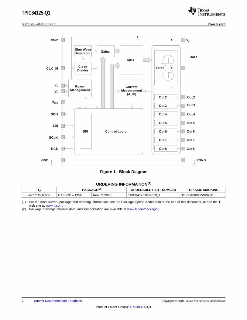
1FEATURES• Output Stage Consists of Eight Programmable • Divider Block Generates an Internal Frequency
Half-Bridge MOSFET Drivers (Configurable in From the Input Clock (Main Controller); UsedHalf, Full, or Parallel Bridges) Which Deliver for the Internal LogicModulated Current to Each Coil • Sophisticated Failure Detection and Handling
• Linear Mode Output: Generates a Sine Wave • HTSSOP (PWP) 28-Pin PackageVoltage That is Controlled by the • Operating Temperature Range:Microcontroller -40°C to +105°C
• Output Stage is Overload Protected for Shortand Over Temperature APPLICATIONS
• Driver Control and Diagnosis Blocks Drive the • Automotive Passive Start and Passive EntryGates of the MOSFETS Via Data From the SPI Applications
• Antenna Diagnostics: Short to GND, Short toVBAT, And Open Load Via CurrentMeasurement
DESCRIPTIONThe low-frequency (LF) antenna driver is dedicated to automotive applications requiring passive entry or passivestart operational control. It allows for up to eight dedicated drivers, consisting of MOSFET transistors. The devicealso incorporates sophisticated diagnosis, protection and monitoring features.
1
Please be aware that an important notice concerning availability, standard warranty, and use in critical applications of TexasInstruments semiconductor products and disclaimers thereto appears at the end of this data sheet.
PRODUCTION DATA information is current as of publication date. Copyright © 2010, Texas Instruments IncorporatedProducts conform to specifications per the terms of the TexasInstruments standard warranty. Production processing does notnecessarily include testing of all parameters.
Out 1
Out 2
MUX
CurrentMeasurement
(ADC)
Gains
Out 3
Out 4
Out 5
Out 6
Out 7
Out 8
ClockDivider
Sine WaveGeneration
Out 1
Out 2
Out 3
Out 4
Out 5
Out 6
Out 7
Out 8
VA
VD
RBIAS
SDO
SDI
SCLK
NCS
CLK_IN
VS/2 VS
Control LogicSPI
PGNDGND
PowerManagement
TPIC84125-Q1
SLDS175 –AUGUST 2010 www.ti.com
Figure 1. Block Diagram
ORDERING INFORMATION (1)
TA PACKAGE (2) ORDERABLE PART NUMBER TOP-SIDE MARKING
–40°C to 105°C HTSSOP – PWP Reel of 2000 TPIC84125TPWPRQ1 TPIC84000TPWPRQ1
(1) For the most current package and ordering information, see the Package Option Addendum at the end of this document, or see the TIweb site at www.ti.com.
(2) Package drawings, thermal data, and symbolization are available at www.ti.com/packaging.
2 Submit Documentation Feedback Copyright © 2010, Texas Instruments Incorporated
Product Folder Link(s): TPIC84125-Q1
1
2
3
4
5
6
7
8 21
22
23
24
25
26
27
28
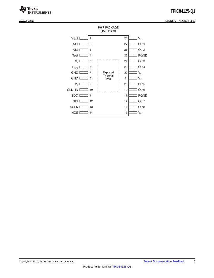
PWP PACKAGE
(TOP VIEW)
VS
Out1
Out2
PGND
Out3
Out4
VS
VS
VS/2
AT1
AT2
Test
VA
RBIAS
GND
GND
9
10
11
12
VD
CLK_IN
SDO
SDI 17
18
19
20 Out5
Out6
PGND
Out7
13
14
SCLK
NCS 15
16 Out8
VS
ExposedThermal
Pad
TPIC84125-Q1
www.ti.com SLDS175 –AUGUST 2010
Copyright © 2010, Texas Instruments Incorporated Submit Documentation Feedback 3
Product Folder Link(s): TPIC84125-Q1
TPIC84125-Q1
SLDS175 –AUGUST 2010 www.ti.com
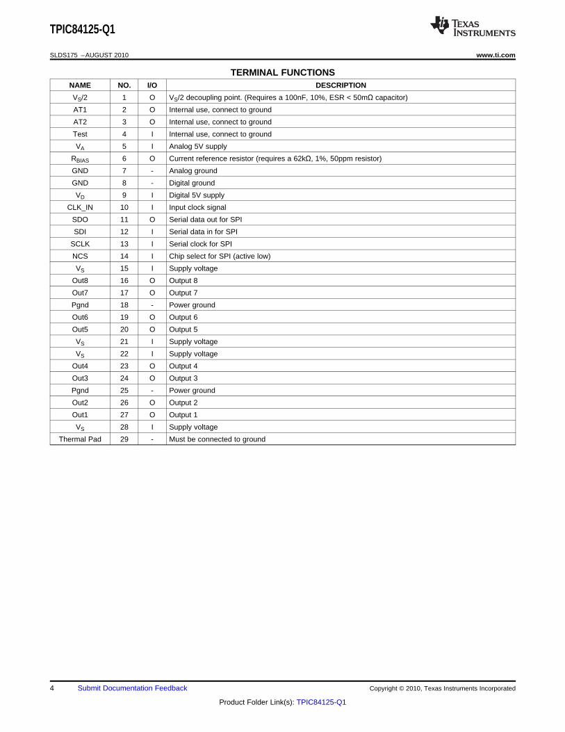
TERMINAL FUNCTIONSNAME NO. I/O DESCRIPTION
VS/2 1 O VS/2 decoupling point. (Requires a 100nF, 10%, ESR < 50mΩ capacitor)
AT1 2 O Internal use, connect to ground
AT2 3 O Internal use, connect to ground
Test 4 I Internal use, connect to ground
VA 5 I Analog 5V supply
RBIAS 6 O Current reference resistor (requires a 62kΩ, 1%, 50ppm resistor)
GND 7 - Analog ground
GND 8 - Digital ground
VD 9 I Digital 5V supply
CLK_IN 10 I Input clock signal
SDO 11 O Serial data out for SPI
SDI 12 I Serial data in for SPI
SCLK 13 I Serial clock for SPI
NCS 14 I Chip select for SPI (active low)
VS 15 I Supply voltage
Out8 16 O Output 8
Out7 17 O Output 7
Pgnd 18 - Power ground
Out6 19 O Output 6
Out5 20 O Output 5
VS 21 I Supply voltage
VS 22 I Supply voltage
Out4 23 O Output 4
Out3 24 O Output 3
Pgnd 25 - Power ground
Out2 26 O Output 2
Out1 27 O Output 1
VS 28 I Supply voltage
Thermal Pad 29 - Must be connected to ground
4 Submit Documentation Feedback Copyright © 2010, Texas Instruments Incorporated
Product Folder Link(s): TPIC84125-Q1
TPIC84125-Q1
www.ti.com SLDS175 –AUGUST 2010
DEVICE INFORMATION
The TPIC84125 is designed to control Passive Entry, Passive Start (PEPS) systems as a part of the central bodycontrol module. Functionally, the TPIC84125 transmits a magnetic field signal via antenna coils locatedthroughout the vehicle. The data is transmitted using amplitude shift keying (ASK). Such a signal is received byan external RFID card or key, which then activates the card or key to then process and send an authenticatingsignal back to the vehicle, thus authenticating the driver. Once authenticated, the driver is able to open doors orstart the vehicle depending on the systems specific configuration. In general, the antenna load of the TPIC84125is a coil, which generates a magnetic field which is high enough to transmit data to the ID card, and accurateenough for location recognition outside of the vehicle.
Functional Description
Power Management
The TPIC84125 operates with three types of supply voltage: Digital 5V (VD), Analog 5V (VA ), and Power (VS).While VD is used for the internal digital circuitry and VA voltage determines:• The accuracy of the output voltage in data and destroy modes, because the sine wave signal is derived from
the VA voltage.• The accuracy of the current measurements, because the Current Measurement (ADC) reference voltage is
derived from the VA voltage.• The supply currents for the IC, as the bias current is derived from the VA voltage.
NOTEVD and VA must be tied together to avoid latch up.
VS must be powered on all VS pins regardless of which outputs are used.
Biasing: Biasing of the circuit is done by an external resistor, RBIAS = 62kΩ, 1%, 50ppm. The value of the RBIASresistance determines:• The accuracy of the current measurements, because the ADC reference voltage is proportional to the VA
voltage divided by the value of RBIAS.• The supply currents for the IC, as the biasing current is proportional to the VA voltage divided by the value of
RBIAS.
Clock Divider
The Clock Divider generates a 2 MHz internal clock signal from the external clock. The internal clock frequencyis used for:• Clearing and latching the fault bits within Control and Status Register (CSR).• For generating the frequency of the sine wave
The divider can be programmed to either: /1, /2, /4, /8, with the default being /8. Table 1 shows the possibleCLK_IN input frequencies to generate 125 kHz signal.
Table 1. Clock Divider
Divider CLK_IN
/1 2 MHz
/2 4 MHz
/4 8 MHz
/8 (default) 16 MHz
Copyright © 2010, Texas Instruments Incorporated Submit Documentation Feedback 5
Product Folder Link(s): TPIC84125-Q1
0
VS/2
VS
0
VS
Out1
Out2
Time
(µs)
( V )
Data 0 1 1 0 1 0
3.9 kBaud (Manchester encoded “100”)
Start 128 256 384 512 640 768
VS/2
TPIC84125-Q1
SLDS175 –AUGUST 2010 www.ti.com
To function properly the following conditions must be satisfied:• The incoming clock (CLK_IN) has to be provided for at least 4 cycles of the internal clock after writing to
Configuration register via SPI• In the case of a wake up command (i.e. sleep bit = 0 in the Config Reg), CLK_IN has to be provided during
124 additional cycles of the internal clock for fault blanking after writing the Config Register. During that time:– Data1 buffer cannot be written to if sending mode bit in Config Reg is set to 1 (autosend mode).– SPI command "Start Transmission" cannot be programmed
• In the case of CSR read and if a fault is cleared then, CLK_IN also has to be provided during a total of 128clock cycles for the same reason of fault blanking.
CLK_IN electrical levels:• When the CLK_IN is OFF, the electrical level should be high (typically 5V)• The clock should be turned OFF after a low to high transition of CLK_IN
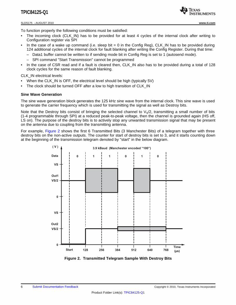
Sine Wave Generation
The sine wave generation block generates the 125 kHz sine wave from the internal clock. This sine wave is usedto generate the carrier frequency which is used for transmitting the signal as well as Destroy bits.
Note that the Destroy bits consist of bringing the selected channel to VS/2, transmitting a small number of bits(1-4 programmable through SPI) at a reduced peak-to-peak voltage, then the channel is grounded again (HS off,LS on). The purpose of the destroy bits is to actively stop any unwanted transmission signal that may be presenton the antenna due to coupling from the transmitting antenna.
For example, Figure 2 shows the first 6 Transmitted Bits (3 Manchester Bits) of a telegram together with threedestroy bits on the non-active outputs. The counter for start of destroy bits is set to 3, and it starts counting downat the beginning of the transmission telegram denoted by "start" in the below diagram.
Figure 2. Transmitted Telegram Sample With Destroy Bits
6 Submit Documentation Feedback Copyright © 2010, Texas Instruments Incorporated
Product Folder Link(s): TPIC84125-Q1
0
VS /2
VS
0
VS/2
VS
Out1
Out2
2 Bytes
Counter for start of
transmission with Gain 2:
16 bits
Counter for transmission
in Gain 2:
Transmitted
Data (Bits)
4 bits
Length of
destroy bits :
8 bits
Counter for start
of destroy bits:
Ga
in2
Ga
in1
Start 8 16 32 56
Ga
in
De
str
oy
( V )
TPIC84125-Q1
www.ti.com SLDS175 –AUGUST 2010
Gains
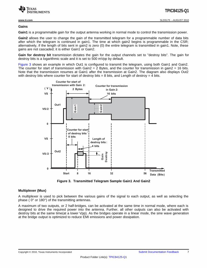
Gain1 is a programmable gain for the output antenna working in normal mode to control the transmission power.
Gain2 allows the user to change the gain of the transmitted telegram for a programmable number of data bitsafter which the telegram is continued in gain1. The time at which gain2 begins is programmable in the CSR;alternatively, if the length of bits sent in gain2 is zero (0) the entire telegram is transmitted in gain1. Note, thesegains are not cascaded; it is either Gain1 or Gain2.
Gain for destroy bit transmission dictates the gain for the output channels set to "destroy bits". The gain fordestroy bits is a logarithmic scale and it is set to 500 mVpp by default.
Figure 3 shows an example in which Out1 is configured to transmit the telegram, using both Gain1 and Gain2.The counter for start of transmission with Gain2 = 2 Bytes, and the counter for transmission in gain2 = 16 bits.Note that the transmission resumes at Gain1 after the transmission at Gain2. The diagram also displays Out2with destroy bits where counter for start of destroy bits = 8 bits, and Length of destroy = 4 bits.
Figure 3. Transmitted Telegram Sample Gain1 And Gain2
Multiplexer (Mux)
A multiplexer is used to pick between the various gains of the signal to each output, as well as selecting thephase ( 0° or 180°) of the transmitting antennas.
A maximum of two outputs, or 2 half-bridges, can be activated at the same time in normal mode, where each isdesigned to drive the required power into the antenna. Further, all other outputs can also be activated withdestroy bits at the same time(at a lower Vpp). As the bridges operate in a linear mode, the sine wave generationat the bridge output is optimized to reduce EMI emissions and power dissipation.
Copyright © 2010, Texas Instruments Incorporated Submit Documentation Feedback 7
Product Folder Link(s): TPIC84125-Q1
I_Antenna
I_LS2
I_LS1
0 8 16 24 32 40 0 8 16 24 32 40
LS1 measurement at first rising edge(Timer1 programmed to 76: 38.275 µs)
Odd rising edge Even rising edge
LS2 measurement at second rising edge(Timer2 programmed to 68: 43.250 µs)
Time(µs)
TPIC84125-Q1
SLDS175 –AUGUST 2010 www.ti.com
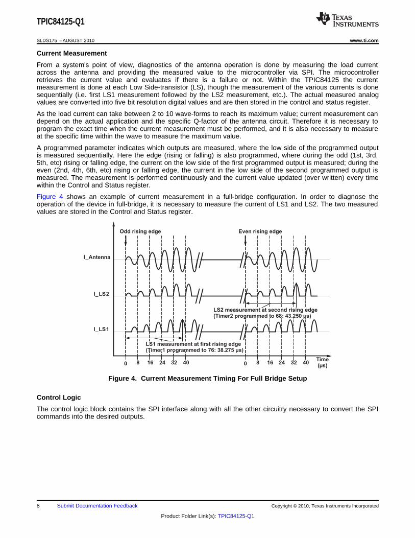
Current Measurement
From a system's point of view, diagnostics of the antenna operation is done by measuring the load currentacross the antenna and providing the measured value to the microcontroller via SPI. The microcontrollerretrieves the current value and evaluates if there is a failure or not. Within the TPIC84125 the currentmeasurement is done at each Low Side-transistor (LS), though the measurement of the various currents is donesequentially (i.e. first LS1 measurement followed by the LS2 measurement, etc.). The actual measured analogvalues are converted into five bit resolution digital values and are then stored in the control and status register.
As the load current can take between 2 to 10 wave-forms to reach its maximum value; current measurement candepend on the actual application and the specific Q-factor of the antenna circuit. Therefore it is necessary toprogram the exact time when the current measurement must be performed, and it is also necessary to measureat the specific time within the wave to measure the maximum value.
A programmed parameter indicates which outputs are measured, where the low side of the programmed outputis measured sequentially. Here the edge (rising or falling) is also programmed, where during the odd (1st, 3rd,5th, etc) rising or falling edge, the current on the low side of the first programmed output is measured; during theeven (2nd, 4th, 6th, etc) rising or falling edge, the current in the low side of the second programmed output ismeasured. The measurement is performed continuously and the current value updated (over written) every timewithin the Control and Status register.
Figure 4 shows an example of current measurement in a full-bridge configuration. In order to diagnose theoperation of the device in full-bridge, it is necessary to measure the current of LS1 and LS2. The two measuredvalues are stored in the Control and Status register.
Figure 4. Current Measurement Timing For Full Bridge Setup
Control Logic
The control logic block contains the SPI interface along with all the other circuitry necessary to convert the SPIcommands into the desired outputs.
8 Submit Documentation Feedback Copyright © 2010, Texas Instruments Incorporated
Product Folder Link(s): TPIC84125-Q1
TPIC84125-Q1
www.ti.com SLDS175 –AUGUST 2010
Operation Modes
There are two operating modes: SLEEP mode and WAKE-UP mode.
In WAKE-UP mode, the device is either ready for the next transmission, or it is transmitting data. The wake-upcommand and the output configuration command are separated to avoid noise on the VS/2 signal at wake up.Note that the start command must happen at least 128 clock cycles after the wake-up command. The devicetransitions from the WAKE-UP mode to the SLEEP mode when the following conditions occur:• The Sleep bit in Configuration Register is set to 1 via SPI
or• An over temperature fault condition is detected
or• VS or VD under voltage is detected
In SLEEP mode, the sine wave generation block is off, the outputs are in tri-state, the SPI is functioning, but theflags are not updated. The device goes from SLEEP mode to WAKE-UP mode when the following conditionsoccur:• The Sleep bit is set to 0 via the SPI
or• The Sleep bit is set to 0 via the SPI and the CSR is read in case of an over temperature detection or VS
under voltage
NOTEWhen operating in the tri-state mode, there is a pull down of typically 150 kΩ at the Outxpins.
Diagnosis
As a function of protecting the TPIC84125 various diagnostic features such as over temperature warning, overtemperature pre-warning and energy limiting protection have been implemented. Flags within a register are usedto highlight a particular fault, or diagnosis, to the main controller, where each fault is essentially latched within theregister until it is read by SPI interface. After having been read by the SPI, the register is then cleared. Thisprotection scheme is implemented within the TPIC84125 itself, as follows:
Over Temperature
When over-temperature occurs while the device is operating in WAKE-UP mode; where upon over temperaturethe device goes to SLEEP mode and the "over temperature" and "failure" flags are set to 1 in the CSR.
If the device is in SLEEP mode, it stays in this mode but no SPI flag is updated.
Temperature Pre-Warning
Temperature pre-warning has no impact on the operating mode of the device. If the device is in WAKE-UPmode, the "temperature pre-warning" flag is set to 1 in the CSR; if the device is in SLEEP mode, no SPI flag isupdated.
Under Voltage• VS under voltage: Occurs when VS goes below the VS under voltage threshold
– If the device is in WAKE-UP mode, it goes to SLEEP mode and the "under voltage at VS" and "failure"flags are set to 1 in the CSR.
– If the device is in SLEEP mode, it stays in this mode but no SPI flag is updated.• VD under voltage: Occurs when VD goes below the VD under voltage
– If the device is in WAKE-UP mode, it goes to SLEEP mode and the "under voltage at VD" and "failure"flags are set to 1 in the CSR.
– If the device is in SLEEP mode, it stays in this mode but no SPI flag is updated.
Copyright © 2010, Texas Instruments Incorporated Submit Documentation Feedback 9
Product Folder Link(s): TPIC84125-Q1
TPIC84125-Q1
SLDS175 –AUGUST 2010 www.ti.com
IFAULT Flag: Energy Limiting Scheme
Two types of output device energy limiting schemes are used:1. Detection of DC currents flowing in the output transistors
In normal operation, with an AC coupled load, continuous DC currents of greater than several mA will notflow in the output transistors. If a current greater than 150mA (nominal) flows in either output transistor for aduration greater than 4ms then the IFAULT condition will be activated and that channel will be placed intri-state. The exact time before the IFAULT is activated is a function of the voltage across the transistorconducting >150mA load current. Larger voltages across this transistor will cause the deglitch time to beshorter. With VS = 38V and with the output at VS/2 the minimum deglitch time is 4ms. The deglitch timer isreset when the current level falls below 150mA.
2. Detection of excess bi-directional peak currents flowing in the output transistors
If a current greater than 0.9A flows in both output transistors when the sine wave signal is driven through theoutput transistors, then the IFAULT condition will be activated and that channel will be placed in tri-state. TheIFAULT condition is activated when both high side and low side transistors have conducted >0.9A at anytime during the sine wave burst. The IFAULT signal will be activated immediately when the second outputtransistor current exceeds 0.9A. The high side and low side detectors are reset during the transmission of a"0" bit.
IFAULT has no impact on the operating mode.• If the device is in WAKE-UP mode, the "IFAULT" and "failure" flags are set to 1 in the CSR and the channel
which has failed is put in tri-state.• If the device is in SLEEP mode, no SPI flag is updated. However the data buffer will continue to be read out
until software stops the data buffer read by sending new Configuration data.
SPI Interface
A Serial Peripheral Interface (SPI) circuit is integrated into the device to set various internal registers and readout current measurement and status information from the drivers. TPIC84125 operates in slave mode and themicrocontroller always acts as a master. The interface to the external micro-controller consists of 4 pins: NCS,SCLK, SDO and SDI.
SPI Frame Structure
Each SPI communication frame for the TPIC84125 has a length of 64 bits, where it is forbidden to send morethan 64 bits. Each 64bit frame consists of 8 command-bits and 56-data-bits. The format of the 64 bits entering atSDI and sent out at SDO is shown in Figure 5:
Figure 5. SPI Frame Structure
The MSB is the first "in" at the SDI and first "out" at the SDO, where the command sent out on SDO is thecommand that was sent in the SDI's previous cycle
When NCS is high, any signals at the SCLK and SDI pins are ignored, and the SDO is forced into a highimpedance state.
During a High to Low transition on NCS, the SPI response word is loaded into a shift register, where the SCLKpin must be low when NCS goes low.
At each rising edge of SCLK after NCS goes low, the response bit is serially shifted out on the SDO pin. Further,the Control and Status register has to be cleared after readout at next NCS falling edge.
10 Submit Documentation Feedback Copyright © 2010, Texas Instruments Incorporated
Product Folder Link(s): TPIC84125-Q1
Bit63 Bit62 Bit61 Bit60 Bit2 Bit1 Bit0
R63
D63
R62 R61 R60 R2 R1 R0
D62 D61 D60 D2 D1 D0
NCS
SCLK
SDO
SDI
TPIC84125-Q1
www.ti.com SLDS175 –AUGUST 2010
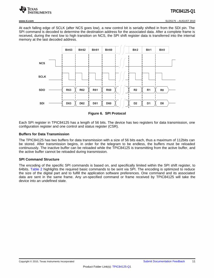
At each falling edge of SCLK (after NCS goes low), a new control bit is serially shifted in from the SDI pin. TheSPI command is decoded to determine the destination address for the associated data. After a complete frame isreceived, during the next low to high transition on NCS, the SPI shift register data is transferred into the internalmemory at the last decoded address.
Figure 6. SPI Protocol
Each SPI register in TPIC84125 has a length of 56 bits. The device has two registers for data transmission, oneconfiguration register and one control and status register (CSR).
Buffers for Data Transmission
The TPIC84125 has two buffers for data transmission with a size of 56 bits each, thus a maximum of 112bits canbe stored. After transmission begins, in order for the telegram to be endless, the buffers must be reloadedcontinuously. The inactive buffer can be reloaded while the TPIC84125 is transmitting from the active buffer, andthe active buffer cannot be reloaded during transmission.
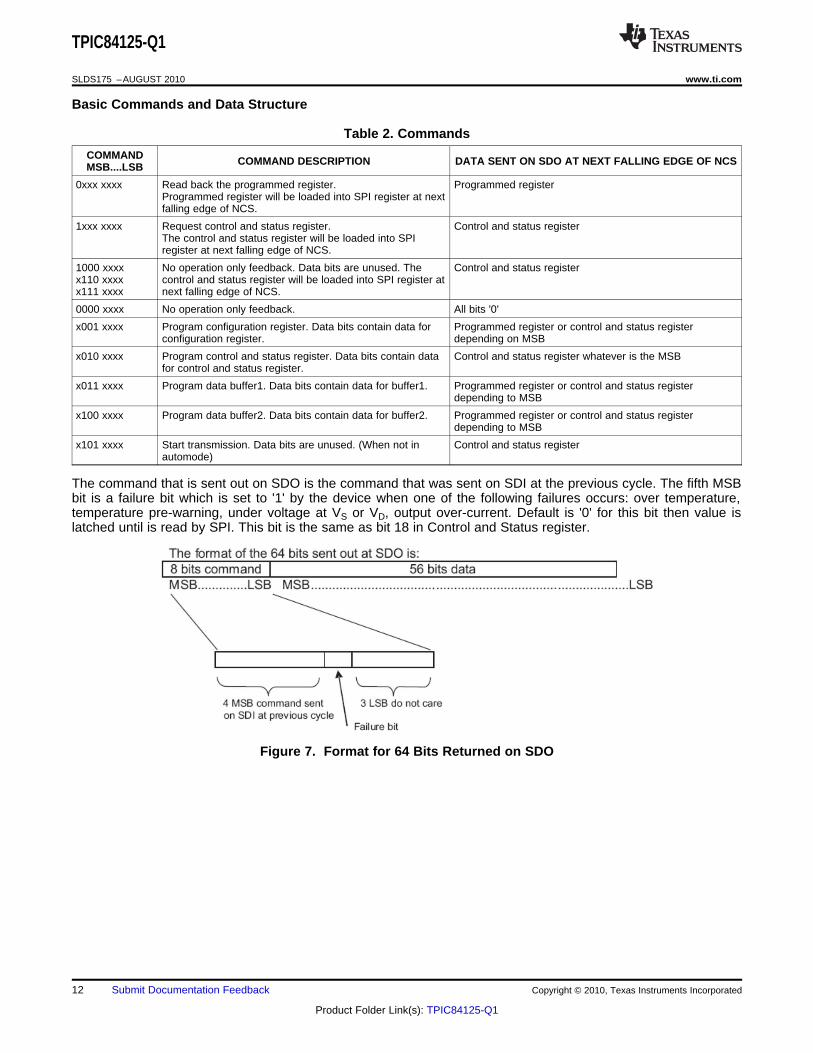
SPI Command Structure
The encoding of the specific SPI commands is based on, and specifically limited within the SPI shift register, to64bits. Table 2 highlights the required basic commands to be sent via SPI. The encoding is optimized to reducethe size of the digital part and to fulfill the application software preferences. One command and its associateddata are sent in the same frame. Any un-specified command or frame received by TPIC84125 will take thedevice into an undefined state.
Copyright © 2010, Texas Instruments Incorporated Submit Documentation Feedback 11
Product Folder Link(s): TPIC84125-Q1
TPIC84125-Q1
SLDS175 –AUGUST 2010 www.ti.com
Basic Commands and Data Structure
Table 2. Commands
COMMAND COMMAND DESCRIPTION DATA SENT ON SDO AT NEXT FALLING EDGE OF NCSMSB....LSB
0xxx xxxx Read back the programmed register. Programmed registerProgrammed register will be loaded into SPI register at nextfalling edge of NCS.
1xxx xxxx Request control and status register. Control and status registerThe control and status register will be loaded into SPIregister at next falling edge of NCS.
1000 xxxx No operation only feedback. Data bits are unused. The Control and status registerx110 xxxx control and status register will be loaded into SPI register atx111 xxxx next falling edge of NCS.
0000 xxxx No operation only feedback. All bits '0'
x001 xxxx Program configuration register. Data bits contain data for Programmed register or control and status registerconfiguration register. depending on MSB
x010 xxxx Program control and status register. Data bits contain data Control and status register whatever is the MSBfor control and status register.
x011 xxxx Program data buffer1. Data bits contain data for buffer1. Programmed register or control and status registerdepending to MSB
x100 xxxx Program data buffer2. Data bits contain data for buffer2. Programmed register or control and status registerdepending to MSB
x101 xxxx Start transmission. Data bits are unused. (When not in Control and status registerautomode)
The command that is sent out on SDO is the command that was sent on SDI at the previous cycle. The fifth MSBbit is a failure bit which is set to '1' by the device when one of the following failures occurs: over temperature,temperature pre-warning, under voltage at VS or VD, output over-current. Default is '0' for this bit then value islatched until is read by SPI. This bit is the same as bit 18 in Control and Status register.
Figure 7. Format for 64 Bits Returned on SDO
12 Submit Documentation Feedback Copyright © 2010, Texas Instruments Incorporated
Product Folder Link(s): TPIC84125-Q1
TPIC84125-Q1
www.ti.com SLDS175 –AUGUST 2010
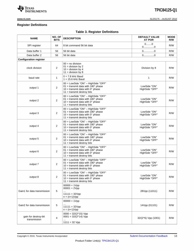
Register Definitions
Table 3. Register Definitions
NO. OF DEFAULT VALUE MODENAME DESCRIPTIONBITS AT POR R/W
0........0SPI register 64 8 bit command 56 bit data R/W0...............0
Data buffer 1 56 56 bit data 0...............0 R/W
Data buffer 2 56 56 bit data 0...............0 R/W
Configuration register
00 = no division01 = division by 2clock division 2 Division by 8 R/W10 = division by 411 = division by 8
0 = 7.8 kHz Baudbaud rate 1 1 R/W1 = 15.6 kHz Baud
00 = LowSide "ON" – HighSide "OFF"01 = transmit data with 180° phase LowSide "ON"output 1 2 R/W10 = transmit data with 0° phase HighSide "OFF"11 = transmit destroy bits
00 = LowSide "ON" – HighSide "OFF"01 = transmit data with 180° phase LowSide "ON"output 2 2 R/W10 = transmit data with 0° phase HighSide "OFF"11 = transmit destroy bits
00 = LowSide "ON" – HighSide "OFF"01 = transmit data with 180° phase LowSide "ON"output 3 2 R/W10 = transmit data with 0° phase HighSide "OFF"11 = transmit destroy bits
00 = LowSide "ON" – HighSide "OFF"01 = transmit data with 180° phase LowSide "ON"output 4 2 R/W10 = transmit data with 0° phase HighSide "OFF"11 = transmit destroy bits
00 = LowSide "ON" – HighSide "OFF"01 = transmit data with 180° phase LowSide "ON"output 5 2 R/W10 = transmit data with 0° phase HighSide "OFF"11 = transmit destroy bits
00 = LowSide "ON" – HighSide "OFF"01 = transmit data with 180° phase LowSide "ON"output 6 2 R/W10 = transmit data with 0° phase HighSide "OFF"11 = transmit destroy bits
00 = LowSide "ON" – HighSide "OFF"01 = transmit data with 180° phase LowSide "ON"output 7 2 R/W10 = transmit data with 0° phase HighSide "OFF"11 = transmit destroy bits
00 = LowSide "ON" – HighSide "OFF"01 = transmit data with 180° phase LowSide "ON"output 8 2 R/W10 = transmit data with 0° phase HighSide "OFF"11 = transmit destroy bits
00000 = 1Vpp00001 = 2Vpp
Gain1 for data transmission 5 … 28Vpp (11011) R/W11111 = 32Vppn = (n+1)Vpp
00000 = 1Vpp…Gain2 for data transmission 5 14Vpp (01101) R/W11111 = 32Vppn = (n+1)Vpp
0000 = 32/(2^15) Vppgain for destroy-bit 0001 = 32/(2^14) Vpp4 32/(2^6) Vpp (1001) R/Wtransmission …
1111 = 32 Vpp
Copyright © 2010, Texas Instruments Incorporated Submit Documentation Feedback 13
Product Folder Link(s): TPIC84125-Q1
TPIC84125-Q1
SLDS175 –AUGUST 2010 www.ti.com
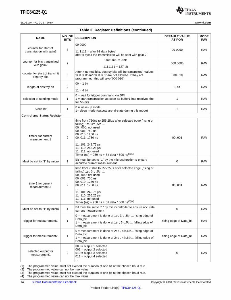
Table 3. Register Definitions (continued)
NO. OF DEFAULT VALUE MODENAME DESCRIPTIONBITS AT POR R/W
00 0000counter for start of …6 00 0000 R/Wtransmission with gain2 11 1111 = after 63 data bytes
after x bytes the transmission will be sent with gain 2
000 0000 = 0 bitcounter for bits transmitted 7 … 000 0000 R/Wwith gain2 1111111 = 127 bit
After x normal bits, destroy bits will be transmitted. Valuescounter for start of transmit 6 '000 000' and '000 001' are not allowed. If they are 000 010 R/Wdestroy bits programmed, this will give '000 010'.
00 = 1 bitlength of destroy bit 2 … 1 bit R/W
11 = 4 bit
0 = wait for trigger command via SPIselection of sending mode 1 1 = start transmission as soon as buffer1 has received the 1 R/W
full 56 bits
0 = wake-up modeSleep bit 1 1 R/W1= sleep mode (outputs are tri-state during this mode)
Control and Status Register
time from 750ns to 255.25µs after selected edge (rising orfalling) 1st, 3rd ,5th ...00...000: not used00..001: 750 ns00..010: 1250 nstimer1 for current 9 00..011: 1750 ns 00..001 R/Wmeasurement 1 …11..101: 249.75 µs11..110: 255.25 µs11..111: not usedTimer (ns) = 250 ns + Bit data * 500 ns (1) (2)
Bit must be set to "1" by the microcontroller to ensureMust be set to "1" by micro 1 0 R/Waccurate current measurement
time from 750ns to 255.25µs after selected edge (rising orfalling) 1st, 3rd ,5th ...00...000: not used00..001: 750 ns00..010: 1250 nstimer2 for current 9 00..011: 1750 ns 00..001 R/Wmeasurement 2 …11..101: 249.75 µs11..110: 255.25 µs11..111: not usedTimer (ns) = 250 ns + Bit data * 500 ns (3) (4)
Bit must be set to "1" by microcontroller to ensure accurateMust be set to "1" by micro 1 0 R/Wcurrent measurement
0 = measurement is done at 1st, 3rd ,5th ... rising edge ofData_bittrigger for measurement1 1 rising edge of Data_bit R/W1 = measurement is done at 1st , 3rd,5th... falling edge ofData_bit
0 = measurement is done at 2nd , 4th,6th... rising edge ofData_bittrigger for measurement2 1 rising edge of Data_bit R/W1 = measurement is done at 2nd , 4th,6th... falling edge ofData_bit
000 = output 1 selected001 = output 2 selectedselected output for 3 010 = output 3 selected 0 R/Wmeasurement1 011 = output 4 selected…
(1) The programmed value must not exceed the duration of one bit at the chosen baud rate.(2) The programmed value can not be max value.(3) The programmed value must not exceed the duration of one bit at the chosen baud rate.(4) The programmed value can not be max value.
14 Submit Documentation Feedback Copyright © 2010, Texas Instruments Incorporated
Product Folder Link(s): TPIC84125-Q1
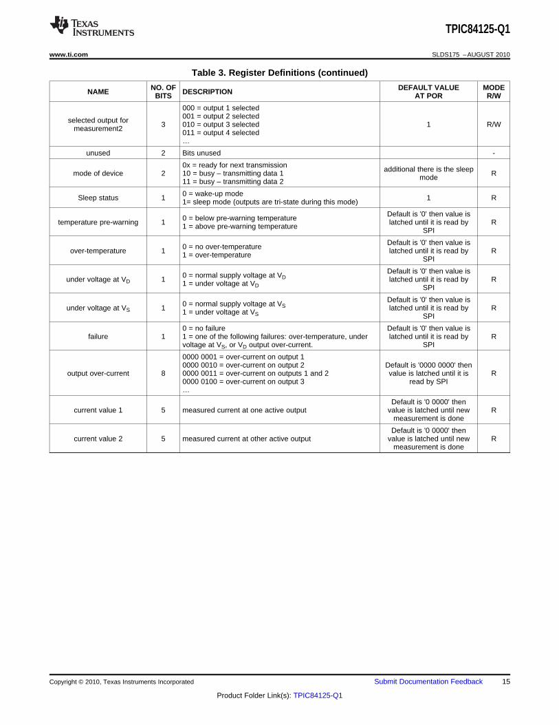
TPIC84125-Q1
www.ti.com SLDS175 –AUGUST 2010
Table 3. Register Definitions (continued)
NO. OF DEFAULT VALUE MODENAME DESCRIPTIONBITS AT POR R/W
000 = output 1 selected001 = output 2 selectedselected output for 3 010 = output 3 selected 1 R/Wmeasurement2 011 = output 4 selected…
unused 2 Bits unused -
0x = ready for next transmission additional there is the sleepmode of device 2 10 = busy – transmitting data 1 Rmode11 = busy – transmitting data 2
0 = wake-up modeSleep status 1 1 R1= sleep mode (outputs are tri-state during this mode)
Default is '0' then value is0 = below pre-warning temperaturetemperature pre-warning 1 latched until it is read by R1 = above pre-warning temperature SPI
Default is '0' then value is0 = no over-temperatureover-temperature 1 latched until it is read by R1 = over-temperature SPI
Default is '0' then value is0 = normal supply voltage at VDunder voltage at VD 1 latched until it is read by R1 = under voltage at VD SPI
Default is '0' then value is0 = normal supply voltage at VSunder voltage at VS 1 latched until it is read by R1 = under voltage at VS SPI
0 = no failure Default is '0' then value isfailure 1 1 = one of the following failures: over-temperature, under latched until it is read by R
voltage at VS, or VD output over-current. SPI
0000 0001 = over-current on output 10000 0010 = over-current on output 2 Default is '0000 0000' then
output over-current 8 0000 0011 = over-current on outputs 1 and 2 value is latched until it is R0000 0100 = over-current on output 3 read by SPI…
Default is '0 0000' thencurrent value 1 5 measured current at one active output value is latched until new R
measurement is done
Default is '0 0000' thencurrent value 2 5 measured current at other active output value is latched until new R
measurement is done
Copyright © 2010, Texas Instruments Incorporated Submit Documentation Feedback 15
Product Folder Link(s): TPIC84125-Q1
TPIC84125-Q1
SLDS175 –AUGUST 2010 www.ti.com
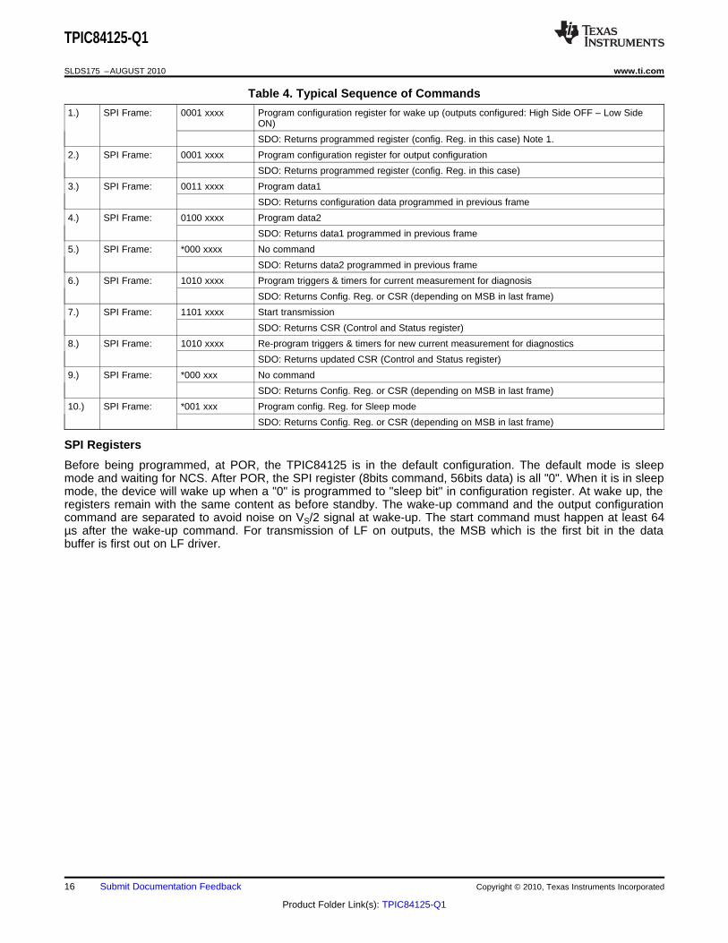
Table 4. Typical Sequence of Commands
1.) SPI Frame: 0001 xxxx Program configuration register for wake up (outputs configured: High Side OFF – Low SideON)
SDO: Returns programmed register (config. Reg. in this case) Note 1.
2.) SPI Frame: 0001 xxxx Program configuration register for output configuration
SDO: Returns programmed register (config. Reg. in this case)
3.) SPI Frame: 0011 xxxx Program data1
SDO: Returns configuration data programmed in previous frame
4.) SPI Frame: 0100 xxxx Program data2
SDO: Returns data1 programmed in previous frame
5.) SPI Frame: *000 xxxx No command
SDO: Returns data2 programmed in previous frame
6.) SPI Frame: 1010 xxxx Program triggers & timers for current measurement for diagnosis
SDO: Returns Config. Reg. or CSR (depending on MSB in last frame)
7.) SPI Frame: 1101 xxxx Start transmission
SDO: Returns CSR (Control and Status register)
8.) SPI Frame: 1010 xxxx Re-program triggers & timers for new current measurement for diagnostics
SDO: Returns updated CSR (Control and Status register)
9.) SPI Frame: *000 xxx No command
SDO: Returns Config. Reg. or CSR (depending on MSB in last frame)
10.) SPI Frame: *001 xxx Program config. Reg. for Sleep mode
SDO: Returns Config. Reg. or CSR (depending on MSB in last frame)
SPI Registers
Before being programmed, at POR, the TPIC84125 is in the default configuration. The default mode is sleepmode and waiting for NCS. After POR, the SPI register (8bits command, 56bits data) is all "0". When it is in sleepmode, the device will wake up when a "0" is programmed to "sleep bit" in configuration register. At wake up, theregisters remain with the same content as before standby. The wake-up command and the output configurationcommand are separated to avoid noise on VS/2 signal at wake-up. The start command must happen at least 64µs after the wake-up command. For transmission of LF on outputs, the MSB which is the first bit in the databuffer is first out on LF driver.
16 Submit Documentation Feedback Copyright © 2010, Texas Instruments Incorporated
Product Folder Link(s): TPIC84125-Q1
GND
GND
GND
GND
5V
12
C1
0.1uF, 0805, 100V, 10%, X7R, ESR<50mOhm
R1
62k, 0805, 1/10W, .5%, 25ppm
CLK_IN
SDO
SDI
SCLK
NCSVs
Vs
Vs
Out8
Out7
Out6
Out5
Out4
Out3
Out2
Out1VS2_decoup
1
AT12
AT23
Test4
VA5
Rbias6
AGND7
DGND8
VD9
CLK_IN10
SDO11
SDI12
SCLK13
NCS14
VS15
Out816
Out717
PGND18
Out619
Out520
VS21
VS22
Out423
Out324
PGND25
Out226
Out127
VS28
U1
GND
R2
R3
12
C_ant
12
C_ant
R4
5V
L_ant
L_ant
GND
TPIC84125-Q1
www.ti.com SLDS175 –AUGUST 2010
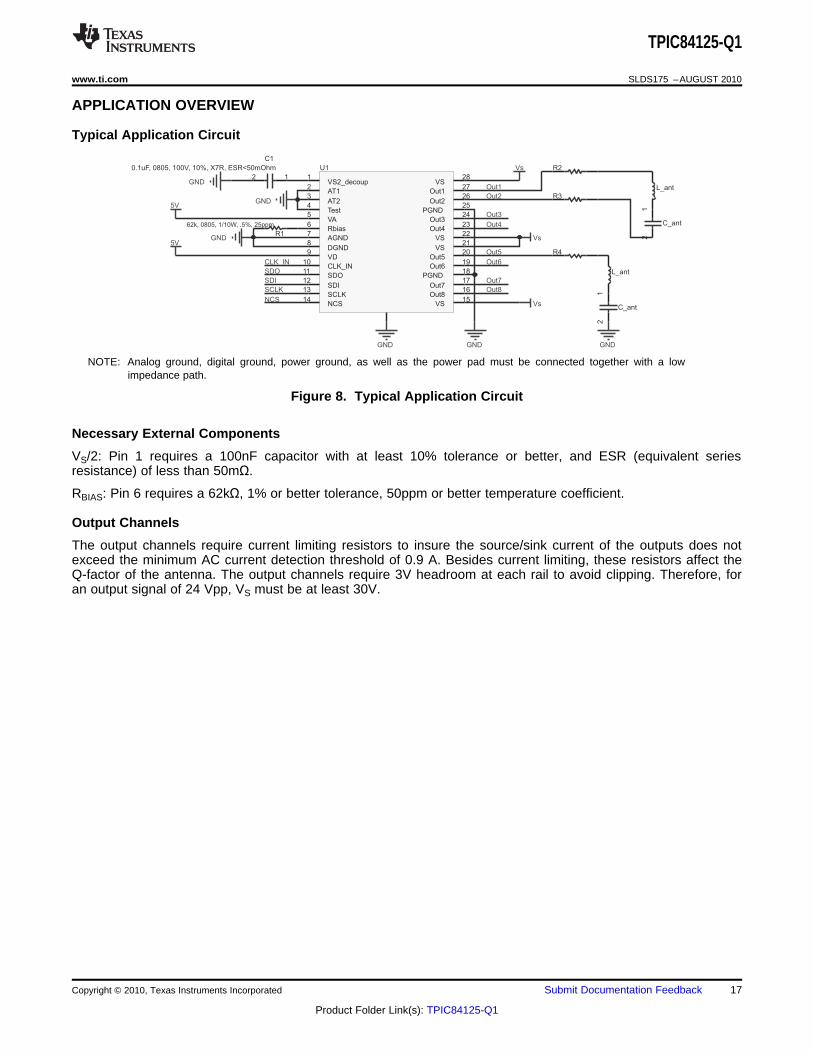
APPLICATION OVERVIEW
Typical Application Circuit
NOTE: Analog ground, digital ground, power ground, as well as the power pad must be connected together with a lowimpedance path.
Figure 8. Typical Application Circuit
Necessary External Components
VS/2: Pin 1 requires a 100nF capacitor with at least 10% tolerance or better, and ESR (equivalent seriesresistance) of less than 50mΩ.
RBIAS: Pin 6 requires a 62kΩ, 1% or better tolerance, 50ppm or better temperature coefficient.
Output Channels
The output channels require current limiting resistors to insure the source/sink current of the outputs does notexceed the minimum AC current detection threshold of 0.9 A. Besides current limiting, these resistors affect theQ-factor of the antenna. The output channels require 3V headroom at each rail to avoid clipping. Therefore, foran output signal of 24 Vpp, VS must be at least 30V.
Copyright © 2010, Texas Instruments Incorporated Submit Documentation Feedback 17
Product Folder Link(s): TPIC84125-Q1
TPIC84125-Q1
SLDS175 –AUGUST 2010 www.ti.com
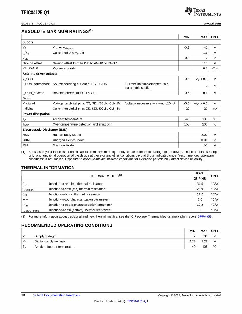
ABSOLUTE MAXIMUM RATINGS (1)
MIN MAX UNIT
Supply
VS Vbat or Vstep-up -0.3 42 V
I_VS Current on one VS pin 1.3 A
VDD -0.3 7 V
Ground offset Ground offset from PGND to AGND or DGND 0.15 V
VS_RAMP VS ramp up rate 0.5 V/µs
Antenna driver outputs
V_Outx -0.3 VS + 0.3 V
I_Outx_source/sink Sourcing/sinking current at HS, LS ON Current limit implemented; see 3 Aparametric section
I_Outx_reverse Reverse current at HS, LS OFF -0.6 0.6 A
Digital
V_digital Voltage on digital pins: CS, SDI, SCLK, CLK_IN Voltage necessary to clamp ±20mA -0.3 VDD + 0.3 V
I_digital Current on digital pins: CS, SDI, SCLK, CLK_IN -20 20 mA
Power dissipation
TA Ambient temperature -40 105 °C
ThSD Over-temperature detection and shutdown 150 205 °C
Electrostatic Discharge (ESD)
HBM Human-Body Model 2000 V
CDM Charged-Device Model 1500 V
MM Machine Model 50 V
(1) Stresses beyond those listed under "absolute maximum ratings" may cause permanent damage to the device. These are stress ratingsonly, and functional operation of the device at these or any other conditions beyond those indicated under "recommended operatingconditions" is not implied. Exposure to absolute-maximum-rated conditions for extended periods may affect device reliability.
THERMAL INFORMATIONPWP
THERMAL METRIC (1) UNIT28 PINS
qJA Junction-to-ambient thermal resistance 34.5 °C/W
qJC(TOP) Junction-to-case(top) thermal resistance 25.9 °C/W
qJB Junction-to-board thermal resistance 14.2 °C/W
ΨJT Junction-to-top characterization parameter 3.6 °C/W
ΨJB Junction-to-board characterization parameter 10.2 °C/W
qJC(BOTTOM) Junction-to-case(bottom) thermal resistance 1.3 °C/W
(1) For more information about traditional and new thermal metrics, see the IC Package Thermal Metrics application report, SPRA953.
RECOMMENDED OPERATING CONDITIONSMIN MAX UNIT
VS Supply voltage 7 38 V
VD Digital supply voltage 4.75 5.25 V
TA Ambient free-air temperature -40 105 °C
18 Submit Documentation Feedback Copyright © 2010, Texas Instruments Incorporated
Product Folder Link(s): TPIC84125-Q1
TPIC84125-Q1
www.ti.com SLDS175 –AUGUST 2010
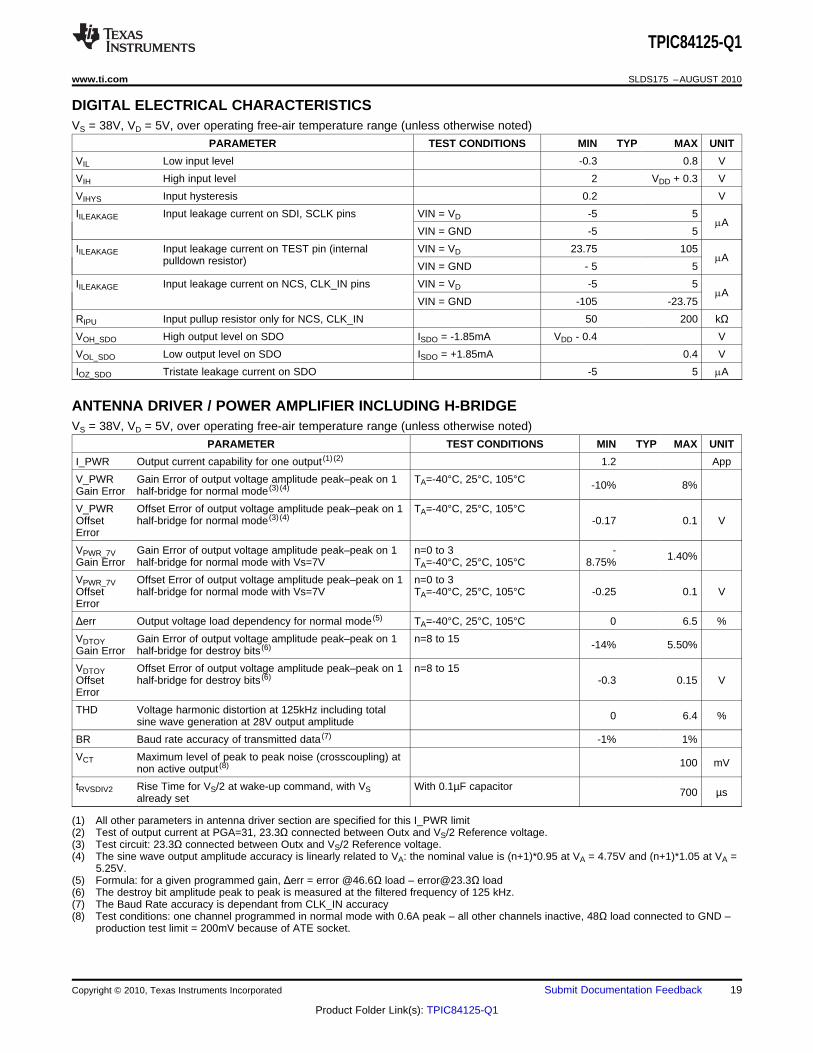
DIGITAL ELECTRICAL CHARACTERISTICSVS = 38V, VD = 5V, over operating free-air temperature range (unless otherwise noted)
PARAMETER TEST CONDITIONS MIN TYP MAX UNIT
VIL Low input level -0.3 0.8 V
VIH High input level 2 VDD + 0.3 V
VIHYS Input hysteresis 0.2 V
IILEAKAGE Input leakage current on SDI, SCLK pins VIN = VD -5 5mA
VIN = GND -5 5
IILEAKAGE Input leakage current on TEST pin (internal VIN = VD 23.75 105mApulldown resistor) VIN = GND - 5 5
IILEAKAGE Input leakage current on NCS, CLK_IN pins VIN = VD -5 5mA
VIN = GND -105 -23.75
RIPU Input pullup resistor only for NCS, CLK_IN 50 200 kΩVOH_SDO High output level on SDO ISDO = -1.85mA VDD - 0.4 V
VOL_SDO Low output level on SDO ISDO = +1.85mA 0.4 V
IOZ_SDO Tristate leakage current on SDO -5 5 mA
ANTENNA DRIVER / POWER AMPLIFIER INCLUDING H-BRIDGEVS = 38V, VD = 5V, over operating free-air temperature range (unless otherwise noted)
PARAMETER TEST CONDITIONS MIN TYP MAX UNIT
I_PWR Output current capability for one output (1) (2) 1.2 App
V_PWR Gain Error of output voltage amplitude peak–peak on 1 TA=-40°C, 25°C, 105°C -10% 8%Gain Error half-bridge for normal mode (3) (4)
V_PWR Offset Error of output voltage amplitude peak–peak on 1 TA=-40°C, 25°C, 105°COffset half-bridge for normal mode (3) (4) -0.17 0.1 VError
VPWR_7V Gain Error of output voltage amplitude peak–peak on 1 n=0 to 3 - 1.40%Gain Error half-bridge for normal mode with Vs=7V TA=-40°C, 25°C, 105°C 8.75%
VPWR_7V Offset Error of output voltage amplitude peak–peak on 1 n=0 to 3Offset half-bridge for normal mode with Vs=7V TA=-40°C, 25°C, 105°C -0.25 0.1 VError
Δerr Output voltage load dependency for normal mode (5) TA=-40°C, 25°C, 105°C 0 6.5 %
VDTOY Gain Error of output voltage amplitude peak–peak on 1 n=8 to 15 -14% 5.50%Gain Error half-bridge for destroy bits (6)
VDTOY Offset Error of output voltage amplitude peak–peak on 1 n=8 to 15Offset half-bridge for destroy bits (6) -0.3 0.15 VError
THD Voltage harmonic distortion at 125kHz including total 0 6.4 %sine wave generation at 28V output amplitude
BR Baud rate accuracy of transmitted data (7) -1% 1%
VCT Maximum level of peak to peak noise (crosscoupling) at 100 mVnon active output (8)
tRVSDIV2 Rise Time for VS/2 at wake-up command, with VS With 0.1µF capacitor 700 µsalready set
(1) All other parameters in antenna driver section are specified for this I_PWR limit(2) Test of output current at PGA=31, 23.3Ω connected between Outx and VS/2 Reference voltage.(3) Test circuit: 23.3Ω connected between Outx and VS/2 Reference voltage.(4) The sine wave output amplitude accuracy is linearly related to VA: the nominal value is (n+1)*0.95 at VA = 4.75V and (n+1)*1.05 at VA =
5.25V.(5) Formula: for a given programmed gain, Δerr = error @46.6Ω load – [email protected]Ω load(6) The destroy bit amplitude peak to peak is measured at the filtered frequency of 125 kHz.(7) The Baud Rate accuracy is dependant from CLK_IN accuracy(8) Test conditions: one channel programmed in normal mode with 0.6A peak – all other channels inactive, 48Ω load connected to GND –
production test limit = 200mV because of ATE socket.
Copyright © 2010, Texas Instruments Incorporated Submit Documentation Feedback 19
Product Folder Link(s): TPIC84125-Q1
TPIC84125-Q1
SLDS175 –AUGUST 2010 www.ti.com
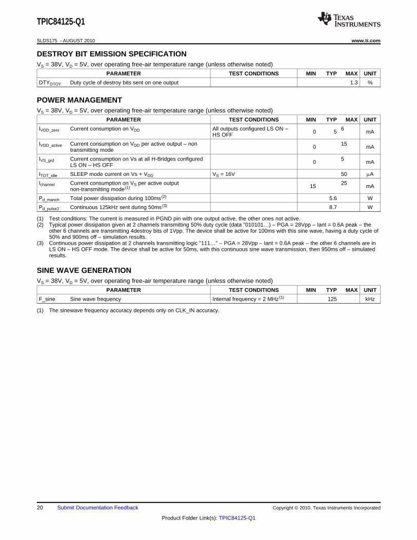
DESTROY BIT EMISSION SPECIFICATIONVS = 38V, VD = 5V, over operating free-air temperature range (unless otherwise noted)
PARAMETER TEST CONDITIONS MIN TYP MAX UNIT
DTYDTOY Duty cycle of destroy bits sent on one output 1.3 %
POWER MANAGEMENTVS = 38V, VD = 5V, over operating free-air temperature range (unless otherwise noted)
PARAMETER TEST CONDITIONS MIN TYP MAX UNIT
IVDD_zero Current consumption on VDD All outputs configured LS ON – 60 5 mAHS OFF
IVDD_active Current consumption on VDD per active output – non 150 mAtransmitting mode
IVS_grd Current consumption on Vs at all H-Bridges configured 50 mALS ON – HS OFF
ITOT_idle SLEEP mode current on Vs + VDD VS = 16V 50 mA
Ichannel Current consumption on VS per active output 2515 mAnon-transmitting mode (1)
Pd_manch Total power dissipation during 100ms (2) 5.6 W
Pd_pulse2 Continuous 125kHz sent during 50ms (3) 8.7 W
(1) Test conditions: The current is measured in PGND pin with one output active, the other ones not active.(2) Typical power dissipation given at 2 channels transmitting 50% duty cycle (data "010101…) – PGA = 28Vpp – Iant = 0.6A peak – the
other 6 channels are transmitting 4destroy bits of 1Vpp. The device shall be active for 100ms with this sine wave, having a duty cycle of50% and 900ms off – simulation results.
(3) Continuous power dissipation at 2 channels transmitting logic "111…" – PGA = 28Vpp – Iant = 0.6A peak – the other 6 channels are inLS ON – HS OFF mode. The device shall be active for 50ms, with this continuous sine wave transmission, then 950ms off – simulatedresults.
SINE WAVE GENERATIONVS = 38V, VD = 5V, over operating free-air temperature range (unless otherwise noted)
PARAMETER TEST CONDITIONS MIN TYP MAX UNIT
F_sine Sine wave frequency Internal frequency = 2 MHz (1) 125 kHz
(1) The sinewave frequency accuracy depends only on CLK_IN accuracy.
20 Submit Documentation Feedback Copyright © 2010, Texas Instruments Incorporated
Product Folder Link(s): TPIC84125-Q1
TPIC84125-Q1
www.ti.com SLDS175 –AUGUST 2010
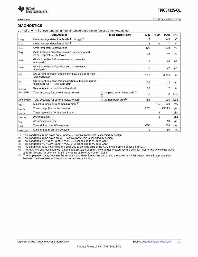
DIAGNOSTICSVS = 38V, VD = 5V, over operating free-air temperature range (unless otherwise noted)
PARAMETER TEST CONDITIONS MIN TYP MAX UNIT
UVDD Under voltage detection threshold on VDD(1) 3 4.5 V
UVS Under voltage detection on VS(2) 3 6 7 V
ThW Over-temperature prewarning 120 170 °C
ThM Delta between Over-temperature prewarning and 23 40 °COver-temperature Shutdown
tcond1 Glitch time filter before over-current protection 4 12 msactivated (3)
tcond2 Glitch time filter before over-current protection 9 22 msactivated (4)
IDC DC current detection threshold in Low Side or in High 0.15 0.375 ASide transistor
IDC DC current detection threshold when output configured 0.5 1.2 A"High Side OFF – Low Side ON"
IAcpeak Resonant current detection threshold 0.9 2 A
Acc_IMP Total accuracy for current measurement In the peak area ( timer code 7, -2 2 LSB8)
Acc_IMNP Total accuracy for current measurement In the non-peak area (5) -2.5 2.5 LSB
Irge_IM Maximum peak current measurement (6) 775 800 mA
trge_IM Timer range (for the two timers) 0.75 255.25 µs
tres_IM Timer resolution (for the two timers) 9 bits
ResA/D A/D resolution 5 bits
tA/D A/D conversion time 10 µs
tshift Time shift on the A/D measure (7) -350 150 ns
Idetect_IM Minimum peak current detection 0 50 mA
(1) Test conditions: ramp down on VA and VD – Positive hysteresis is specified by design.(2) Test conditions: ramp down on VS – Positive hysteresis is specified by design.(3) Test conditions: VS = 38V, Vantx = VS/2, 24Ω connected to VS or to GND.(4) Test conditions: VS = 16V, Vantx = VS/2, 24Ω connected to VS or to GND.(5) This parameter does not include the error due to the time shift of the ADC measurement specified in "tshift".(6) The ADC is 5-bits resolution with a nominal LSB value of 25mA. Two ranges of accuracy are defined: First for the whole sine wave:
2.5LSB; Second for peak currents in the range of 50mA to 800mA: 2LSB(7) The propagation delay between the zero-crossing detection at sine output and the power amplifier output results in a phase shift
between the timer start and the output current zero-crossing.
Copyright © 2010, Texas Instruments Incorporated Submit Documentation Feedback 21
Product Folder Link(s): TPIC84125-Q1
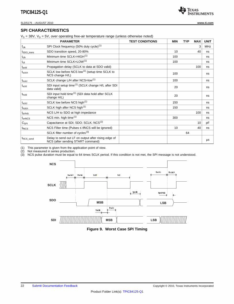
NCS
SCLK
SDO
SDI MSB LSB
MSB LSB
TPIC84125-Q1
SLDS175 –AUGUST 2010 www.ti.com
SPI CHARACTERISTICSVS = 38V, VD = 5V, over operating free-air temperature range (unless otherwise noted)
PARAMETER TEST CONDITIONS MIN TYP MAX UNIT
fclk SPI Clock frequency (50% duty cycle) (1) 3 MHz
tSDO_trans SDO transition speed, 20-80% 10 40 ns
tclh Minimum time SCLK=HIGH (1) 100 ns
tcll Minimum time SCLK=LOW (1) 100 ns
tpcld Propagation delay (SCLK to data at SDO valid) 100 ns
tsclch SCLK low before NCS low (1) (setup time SCLK to 100 nsNCS change H/L)
thclcl SCLK change L/H after NCS=low (1) 100 ns
tscld SDI input setup time (1) (SCLK change H/L after SDI 20 nsdata valid)
thcld SDI input hold time (1) (SDI data hold after SCLK 20 nschange H/L)
tsclcl SCLK low before NCS high (1) 150 ns
thclch SCLK high after NCS high (1) 150 ns
tpchdz NCS L/H to SDO at high impedance 100 ns
tonNCS NCS min. high time (1) 300 ns
CSPI Capacitance at SDI; SDO; SCLK; NCS (2) 10 pF
tfNCS NCS Filter time (Pulses ≤ tfNCS will be ignored) 10 40 ns
SCLK filter number of cycles (3) 64
tNCS_send Delay to send out LF on output after rising edge of µsNCS (after sending START command)
(1) This parameter is given from the application point of view.(2) Not measured in series production.(3) NCS pulse duration must be equal to 64 times SCLK period. If this condition is not met, the SPI message is not understood.
Figure 9. Worst Case SPI Timing
22 Submit Documentation Feedback Copyright © 2010, Texas Instruments Incorporated
Product Folder Link(s): TPIC84125-Q1
IMPORTANT NOTICE
Texas Instruments Incorporated (TI) reserves the right to make corrections, enhancements, improvements and other changes to itssemiconductor products and services per JESD46, latest issue, and to discontinue any product or service per JESD48, latest issue. Buyersshould obtain the latest relevant information before placing orders and should verify that such information is current and complete.TI’s published terms of sale for semiconductor products (http://www.ti.com/sc/docs/stdterms.htm) apply to the sale of packaged integratedcircuit products that TI has qualified and released to market. Additional terms may apply to the use or sale of other types of TI products andservices.Reproduction of significant portions of TI information in TI data sheets is permissible only if reproduction is without alteration and isaccompanied by all associated warranties, conditions, limitations, and notices. TI is not responsible or liable for such reproduceddocumentation. Information of third parties may be subject to additional restrictions. Resale of TI products or services with statementsdifferent from or beyond the parameters stated by TI for that product or service voids all express and any implied warranties for theassociated TI product or service and is an unfair and deceptive business practice. TI is not responsible or liable for any such statements.Buyers and others who are developing systems that incorporate TI products (collectively, “Designers”) understand and agree that Designersremain responsible for using their independent analysis, evaluation and judgment in designing their applications and that Designers havefull and exclusive responsibility to assure the safety of Designers' applications and compliance of their applications (and of all TI productsused in or for Designers’ applications) with all applicable regulations, laws and other applicable requirements. Designer represents that, withrespect to their applications, Designer has all the necessary expertise to create and implement safeguards that (1) anticipate dangerousconsequences of failures, (2) monitor failures and their consequences, and (3) lessen the likelihood of failures that might cause harm andtake appropriate actions. Designer agrees that prior to using or distributing any applications that include TI products, Designer willthoroughly test such applications and the functionality of such TI products as used in such applications.TI’s provision of technical, application or other design advice, quality characterization, reliability data or other services or information,including, but not limited to, reference designs and materials relating to evaluation modules, (collectively, “TI Resources”) are intended toassist designers who are developing applications that incorporate TI products; by downloading, accessing or using TI Resources in anyway, Designer (individually or, if Designer is acting on behalf of a company, Designer’s company) agrees to use any particular TI Resourcesolely for this purpose and subject to the terms of this Notice.TI’s provision of TI Resources does not expand or otherwise alter TI’s applicable published warranties or warranty disclaimers for TIproducts, and no additional obligations or liabilities arise from TI providing such TI Resources. TI reserves the right to make corrections,enhancements, improvements and other changes to its TI Resources. TI has not conducted any testing other than that specificallydescribed in the published documentation for a particular TI Resource.Designer is authorized to use, copy and modify any individual TI Resource only in connection with the development of applications thatinclude the TI product(s) identified in such TI Resource. NO OTHER LICENSE, EXPRESS OR IMPLIED, BY ESTOPPEL OR OTHERWISETO ANY OTHER TI INTELLECTUAL PROPERTY RIGHT, AND NO LICENSE TO ANY TECHNOLOGY OR INTELLECTUAL PROPERTYRIGHT OF TI OR ANY THIRD PARTY IS GRANTED HEREIN, including but not limited to any patent right, copyright, mask work right, orother intellectual property right relating to any combination, machine, or process in which TI products or services are used. Informationregarding or referencing third-party products or services does not constitute a license to use such products or services, or a warranty orendorsement thereof. Use of TI Resources may require a license from a third party under the patents or other intellectual property of thethird party, or a license from TI under the patents or other intellectual property of TI.TI RESOURCES ARE PROVIDED “AS IS” AND WITH ALL FAULTS. TI DISCLAIMS ALL OTHER WARRANTIES ORREPRESENTATIONS, EXPRESS OR IMPLIED, REGARDING RESOURCES OR USE THEREOF, INCLUDING BUT NOT LIMITED TOACCURACY OR COMPLETENESS, TITLE, ANY EPIDEMIC FAILURE WARRANTY AND ANY IMPLIED WARRANTIES OFMERCHANTABILITY, FITNESS FOR A PARTICULAR PURPOSE, AND NON-INFRINGEMENT OF ANY THIRD PARTY INTELLECTUALPROPERTY RIGHTS. TI SHALL NOT BE LIABLE FOR AND SHALL NOT DEFEND OR INDEMNIFY DESIGNER AGAINST ANY CLAIM,INCLUDING BUT NOT LIMITED TO ANY INFRINGEMENT CLAIM THAT RELATES TO OR IS BASED ON ANY COMBINATION OFPRODUCTS EVEN IF DESCRIBED IN TI RESOURCES OR OTHERWISE. IN NO EVENT SHALL TI BE LIABLE FOR ANY ACTUAL,DIRECT, SPECIAL, COLLATERAL, INDIRECT, PUNITIVE, INCIDENTAL, CONSEQUENTIAL OR EXEMPLARY DAMAGES INCONNECTION WITH OR ARISING OUT OF TI RESOURCES OR USE THEREOF, AND REGARDLESS OF WHETHER TI HAS BEENADVISED OF THE POSSIBILITY OF SUCH DAMAGES.Unless TI has explicitly designated an individual product as meeting the requirements of a particular industry standard (e.g., ISO/TS 16949and ISO 26262), TI is not responsible for any failure to meet such industry standard requirements.Where TI specifically promotes products as facilitating functional safety or as compliant with industry functional safety standards, suchproducts are intended to help enable customers to design and create their own applications that meet applicable functional safety standardsand requirements. Using products in an application does not by itself establish any safety features in the application. Designers mustensure compliance with safety-related requirements and standards applicable to their applications. Designer may not use any TI products inlife-critical medical equipment unless authorized officers of the parties have executed a special contract specifically governing such use.Life-critical medical equipment is medical equipment where failure of such equipment would cause serious bodily injury or death (e.g., lifesupport, pacemakers, defibrillators, heart pumps, neurostimulators, and implantables). Such equipment includes, without limitation, allmedical devices identified by the U.S. Food and Drug Administration as Class III devices and equivalent classifications outside the U.S.TI may expressly designate certain products as completing a particular qualification (e.g., Q100, Military Grade, or Enhanced Product).Designers agree that it has the necessary expertise to select the product with the appropriate qualification designation for their applicationsand that proper product selection is at Designers’ own risk. Designers are solely responsible for compliance with all legal and regulatoryrequirements in connection with such selection.Designer will fully indemnify TI and its representatives against any damages, costs, losses, and/or liabilities arising out of Designer’s non-compliance with the terms and provisions of this Notice.
Mailing Address: Texas Instruments, Post Office Box 655303, Dallas, Texas 75265Copyright © 2017, Texas Instruments Incorporated


![AOI [2] Passive Wireless Sensors for Temperature and Corrosion … · 2020. 10. 21. · RFID Sensor Design and Initial Benchtop Testing. • Subtask 2.1: Passive Wireless Design (Q1-6)](https://img.pdfslide.us/doc/110x75/60ddaa273e3ad241ce137ec9/aoi-2-passive-wireless-sensors-for-temperature-and-corrosion-2020-10-21-rfid.jpg)