Embed Size (px)
Citation preview
GND
SpeakerConnector
(Source of ESD) 1 1
22
L Audio IN
Audio AmplifierClass AB
(ESD Sensitive)
R Audio IN
L
R
Audio AmplifierClass AB
(ESD Sensitive)
GND
GND
L Audio
R Audio
Copyright © 2016, Texas Instruments Incorporated
Product
Folder
Sample &Buy
Technical
Documents
Tools &
Software
Support &Community
An IMPORTANT NOTICE at the end of this data sheet addresses availability, warranty, changes, use in safety-critical applications,intellectual property matters and other important disclaimers. PRODUCTION DATA.
TPD1E10B06-Q1SLVSDN7A –AUGUST 2016–REVISED AUGUST 2016
TPD1E10B06-Q1 1-Channel ESD in 0402 Package with 12-pF Capacitance and 6-VBreakdown
1
1 Features1• AEC-Q101 Qualified• IEC 61000-4-2 Level 4 ESD Protection
– ±30-kV Contact Discharge– ±30-kV Air-Gap Discharge
• ISO 10605 (330 pF, 330 Ω) ESD Protection– ±8-kV Contact Discharge– ±15-kV Air-Gap Discharge
• IEC 61000-4-5 Surge Protection– 6 A (8/20 µs)
• I/O Capacitance 12 pF (Typical)• RDYN: 0.38 Ω (Typical)• DC Breakdown Voltage: ±6 V (Minimum)• Ultra low Leakage Current 100 nA (Maximum)• 10-V Clamping Voltage (Typical at IPP = 1 A)• Industrial Temperature Range: –40°C to +125°C• Space-Saving 0402 Footprint
2 Applications• End Equipment:
– Head Unit– Premium Audio– External Amplifier– Body Control Module– Gateway– Telematics– Camera Module
• Interfaces:– Audio Lines– Pushbuttons– Memory Interface– GPIO
3 DescriptionThe TPD1E10B06-Q1 device is a bidirectional TVSESD protection diode in a small 0402 industrystandard package which is convenient for componentplacement in space-saving applications featuring lowRDYN and high IEC rating. The TPD1E10B06-Q1 israted to dissipate ESD strikes above the maximumlevel specified in the IEC 61000-4-2 internationalstandard (Level 4) since ESD voltages can easilyreach 5000 V, which is more than enough to damagemany integrated circuits, but during extremeconditions the voltages can be significantly higher.For example, in a low humidity environment voltagescan exceed 20,000 V.
The low dynamic resistance (0.38 Ω) and lowclamping voltage (10 V at 1-A IPP) ensures systemlevel protection against transient events, providingsufficient protection on designs that are exposed toESD events. This device also features a 12-pF IOcapacitance making it ideal for audio lines, pushbuttons, memory interfaces, or GPIOs.
This device is also available without automotivequalification: TPD1E10B06.
Device Information(1)
PART NUMBER PACKAGE BODY SIZE (NOM)TPD1E10B06-Q1 X1SON (2) 0.60 mm × 1.00 mmTPD1E10B06(2) X1SON (2) 0.60 mm × 1.00 mm
(1) For all available packages, see the orderable addendum atthe end of the data sheet.
(2) This device is not part of the TPD1E10B06-Q1 datasheet,please see TPD1E10B06 for all electrical parameters anddevice characteristics
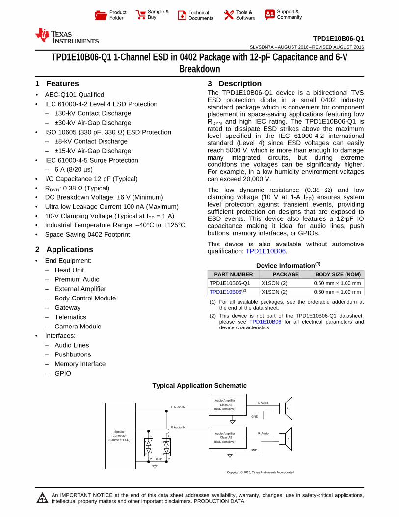
Typical Application Schematic
2
TPD1E10B06-Q1SLVSDN7A –AUGUST 2016–REVISED AUGUST 2016 www.ti.com
Product Folder Links: TPD1E10B06-Q1
Submit Documentation Feedback Copyright © 2016, Texas Instruments Incorporated
Table of Contents1 Features .................................................................. 12 Applications ........................................................... 13 Description ............................................................. 14 Revision History..................................................... 25 Pin Configuration and Functions ......................... 36 Specifications......................................................... 4
6.1 Absolute Maximum Ratings ...................................... 46.2 ESD—AEC Specification Ratings ............................. 46.3 ESD Ratings—IEC Specification .............................. 46.4 ESD Ratings—ISO Specification .............................. 46.5 Recommended Operating Conditions....................... 46.6 Thermal Information .................................................. 46.7 Electrical Characteristics........................................... 56.8 Typical Characteristics .............................................. 6
7 Detailed Description .............................................. 87.1 Overview ................................................................... 87.2 Functional Block Diagram ......................................... 8
7.3 Feature Description................................................... 87.4 Device Functional Modes.......................................... 9
8 Application and Implementation ........................ 108.1 Application Information............................................ 108.2 Typical Application ................................................. 10
9 Power Supply Recommendations ...................... 1210 Layout................................................................... 12
10.1 Layout Guidelines ................................................. 1210.2 Layout Example .................................................... 12
11 Device and Documentation Support ................. 1311.1 Documentation Support ........................................ 1311.2 Receiving Notification of Documentation Updates 1311.3 Community Resources.......................................... 1311.4 Trademarks ........................................................... 1311.5 Electrostatic Discharge Caution............................ 1311.6 Glossary ................................................................ 13
12 Mechanical, Packaging, and OrderableInformation ........................................................... 14
4 Revision History
Changes from Original (August 2016) to Revision A Page
• Changed device status from Product Preview to Production Data ........................................................................................ 1
1
2
3
TPD1E10B06-Q1www.ti.com SLVSDN7A –AUGUST 2016–REVISED AUGUST 2016
Product Folder Links: TPD1E10B06-Q1
Submit Documentation FeedbackCopyright © 2016, Texas Instruments Incorporated
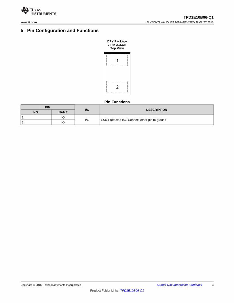
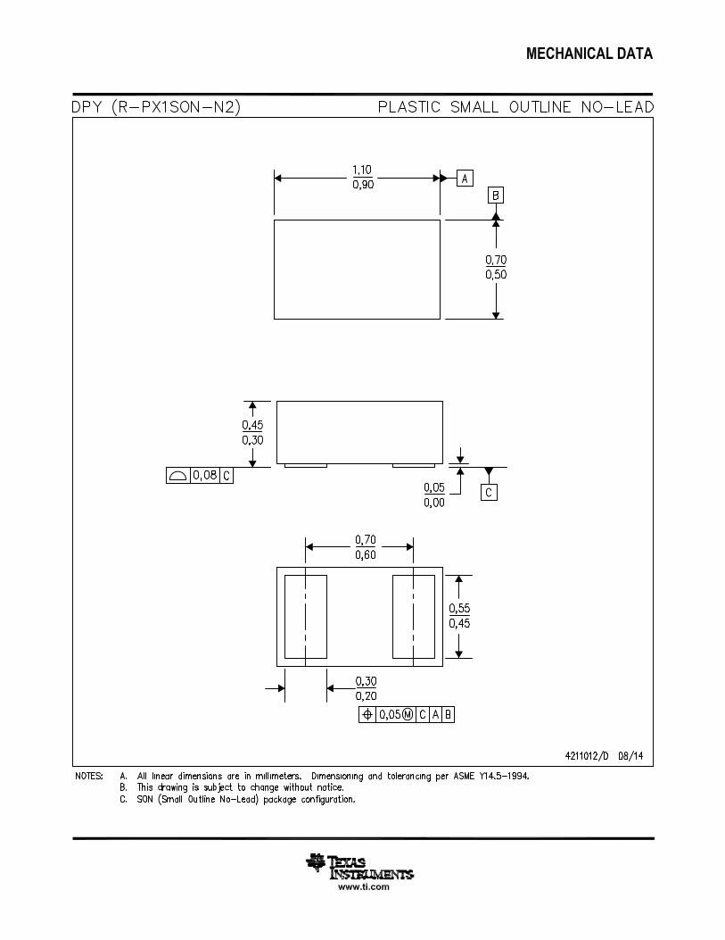
5 Pin Configuration and Functions
DPY Package2-Pin X1SON
Top View
Pin FunctionsPIN
I/O DESCRIPTIONNO. NAME
1 IOI/O ESD Protected I/O. Connect other pin to ground
2 IO
4
TPD1E10B06-Q1SLVSDN7A –AUGUST 2016–REVISED AUGUST 2016 www.ti.com
Product Folder Links: TPD1E10B06-Q1
Submit Documentation Feedback Copyright © 2016, Texas Instruments Incorporated
(1) Stresses beyond those listed under Absolute Maximum Ratings may cause permanent damage to the device. These are stress ratingsonly, which do not imply functional operation of the device at these or any other conditions beyond those indicated under RecommendedOperating Conditions. Exposure to absolute-maximum-rated conditions for extended periods may affect device reliability.
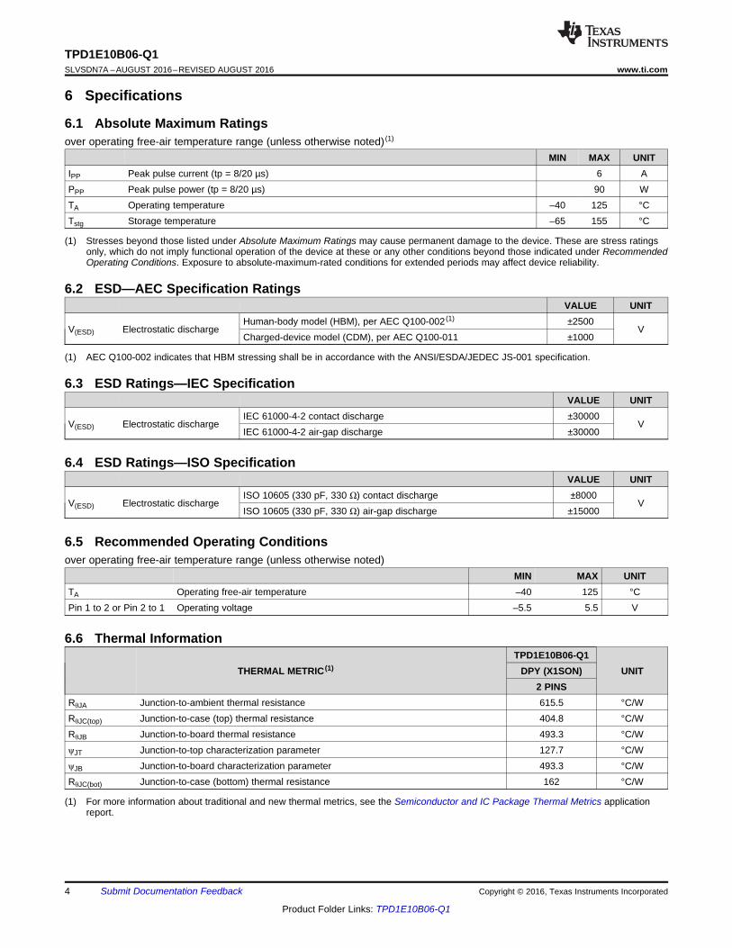
6 Specifications
6.1 Absolute Maximum Ratingsover operating free-air temperature range (unless otherwise noted) (1)
MIN MAX UNITIPP Peak pulse current (tp = 8/20 µs) 6 APPP Peak pulse power (tp = 8/20 µs) 90 WTA Operating temperature –40 125 °CTstg Storage temperature –65 155 °C
(1) AEC Q100-002 indicates that HBM stressing shall be in accordance with the ANSI/ESDA/JEDEC JS-001 specification.
6.2 ESD—AEC Specification RatingsVALUE UNIT
V(ESD) Electrostatic dischargeHuman-body model (HBM), per AEC Q100-002 (1) ±2500
VCharged-device model (CDM), per AEC Q100-011 ±1000
6.3 ESD Ratings—IEC SpecificationVALUE UNIT
V(ESD) Electrostatic dischargeIEC 61000-4-2 contact discharge ±30000
VIEC 61000-4-2 air-gap discharge ±30000
6.4 ESD Ratings—ISO SpecificationVALUE UNIT
V(ESD) Electrostatic dischargeISO 10605 (330 pF, 330 Ω) contact discharge ±8000
VISO 10605 (330 pF, 330 Ω) air-gap discharge ±15000
6.5 Recommended Operating Conditionsover operating free-air temperature range (unless otherwise noted)
MIN MAX UNITTA Operating free-air temperature –40 125 °CPin 1 to 2 or Pin 2 to 1 Operating voltage –5.5 5.5 V
(1) For more information about traditional and new thermal metrics, see the Semiconductor and IC Package Thermal Metrics applicationreport.
6.6 Thermal Information
THERMAL METRIC (1)TPD1E10B06-Q1
UNITDPY (X1SON)2 PINS
RθJA Junction-to-ambient thermal resistance 615.5 °C/WRθJC(top) Junction-to-case (top) thermal resistance 404.8 °C/WRθJB Junction-to-board thermal resistance 493.3 °C/WψJT Junction-to-top characterization parameter 127.7 °C/WψJB Junction-to-board characterization parameter 493.3 °C/WRθJC(bot) Junction-to-case (bottom) thermal resistance 162 °C/W
5
TPD1E10B06-Q1www.ti.com SLVSDN7A –AUGUST 2016–REVISED AUGUST 2016
Product Folder Links: TPD1E10B06-Q1
Submit Documentation FeedbackCopyright © 2016, Texas Instruments Incorporated
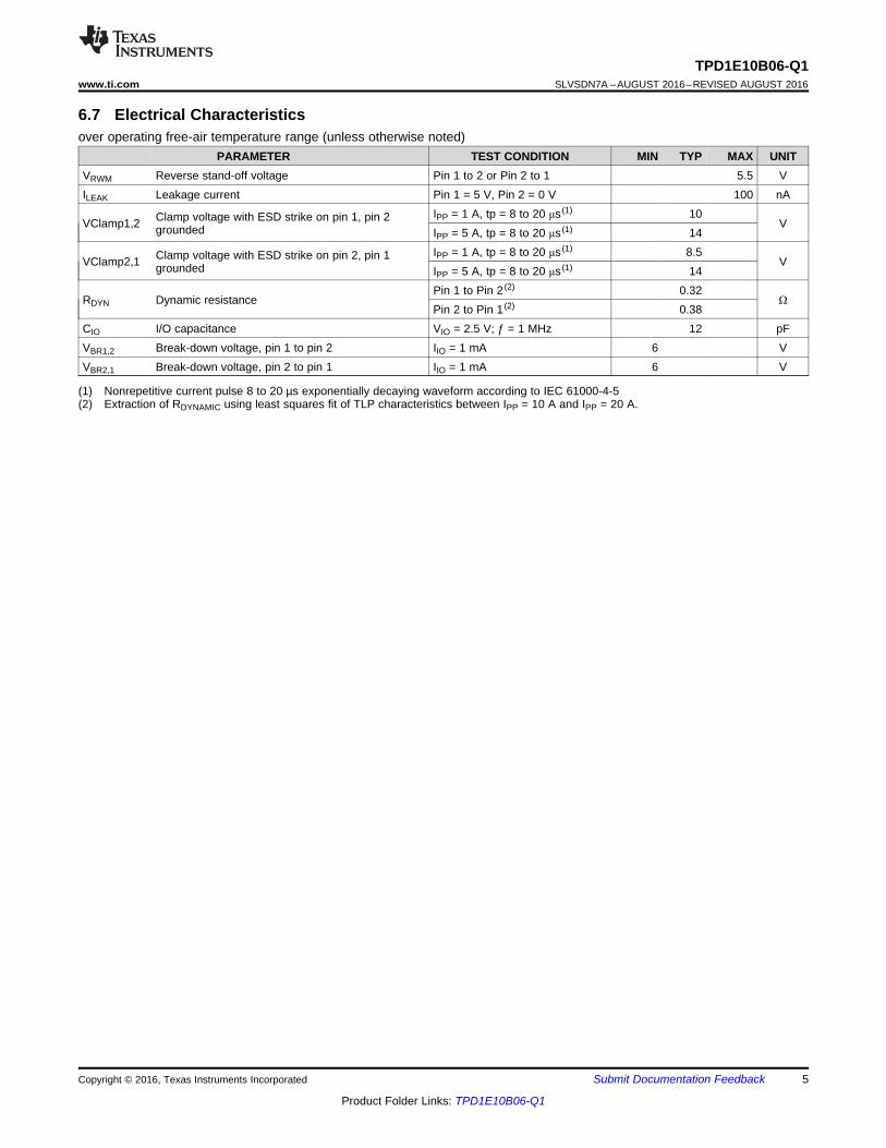
(1) Nonrepetitive current pulse 8 to 20 µs exponentially decaying waveform according to IEC 61000-4-5(2) Extraction of RDYNAMIC using least squares fit of TLP characteristics between IPP = 10 A and IPP = 20 A.
6.7 Electrical Characteristicsover operating free-air temperature range (unless otherwise noted)
PARAMETER TEST CONDITION MIN TYP MAX UNITVRWM Reverse stand-off voltage Pin 1 to 2 or Pin 2 to 1 5.5 VILEAK Leakage current Pin 1 = 5 V, Pin 2 = 0 V 100 nA
VClamp1,2 Clamp voltage with ESD strike on pin 1, pin 2grounded
IPP = 1 A, tp = 8 to 20 μs (1) 10V
IPP = 5 A, tp = 8 to 20 μs (1) 14
VClamp2,1 Clamp voltage with ESD strike on pin 2, pin 1grounded
IPP = 1 A, tp = 8 to 20 μs (1) 8.5V
IPP = 5 A, tp = 8 to 20 μs (1) 14
RDYN Dynamic resistancePin 1 to Pin 2 (2) 0.32
ΩPin 2 to Pin 1 (2) 0.38
CIO I/O capacitance VIO = 2.5 V; ƒ = 1 MHz 12 pFVBR1,2 Break-down voltage, pin 1 to pin 2 IIO = 1 mA 6 VVBR2,1 Break-down voltage, pin 2 to pin 1 IIO = 1 mA 6 V
Time (Ps)
Cur
rent
(A
)
Pow
er (
W)
-10 0 10 20 30 40 50 60 700 0
1 15
2 30
3 45
4 60
5 75
6 90
7 105
8 120
9 135
10 150
D001
CurrentPower
6
TPD1E10B06-Q1SLVSDN7A –AUGUST 2016–REVISED AUGUST 2016 www.ti.com
Product Folder Links: TPD1E10B06-Q1
Submit Documentation Feedback Copyright © 2016, Texas Instruments Incorporated
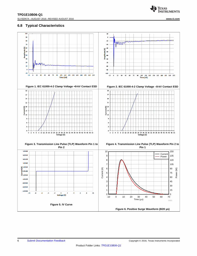
6.8 Typical Characteristics
Figure 1. IEC 61000-4-2 Clamp Voltage +8-kV Contact ESD Figure 2. IEC 61000-4-2 Clamp Voltage –8-kV Contact ESD
Figure 3. Transmission Line Pulse (TLP) Waveform Pin 1 toPin 2
Figure 4. Transmission Line Pulse (TLP) Waveform Pin 2 toPin 1
Figure 5. IV Curve
Figure 6. Positive Surge Waveform (8/20 µs)
Time (Ps)
Cur
rent
(A
)
Pow
er (
W)
-10 0 10 20 30 40 50 60 700 0
1 10
2 20
3 30
4 40
5 50
6 60
7 70
8 80
9 90
10 100
11 110
D002
CurrentPower
7
TPD1E10B06-Q1www.ti.com SLVSDN7A –AUGUST 2016–REVISED AUGUST 2016
Product Folder Links: TPD1E10B06-Q1
Submit Documentation FeedbackCopyright © 2016, Texas Instruments Incorporated
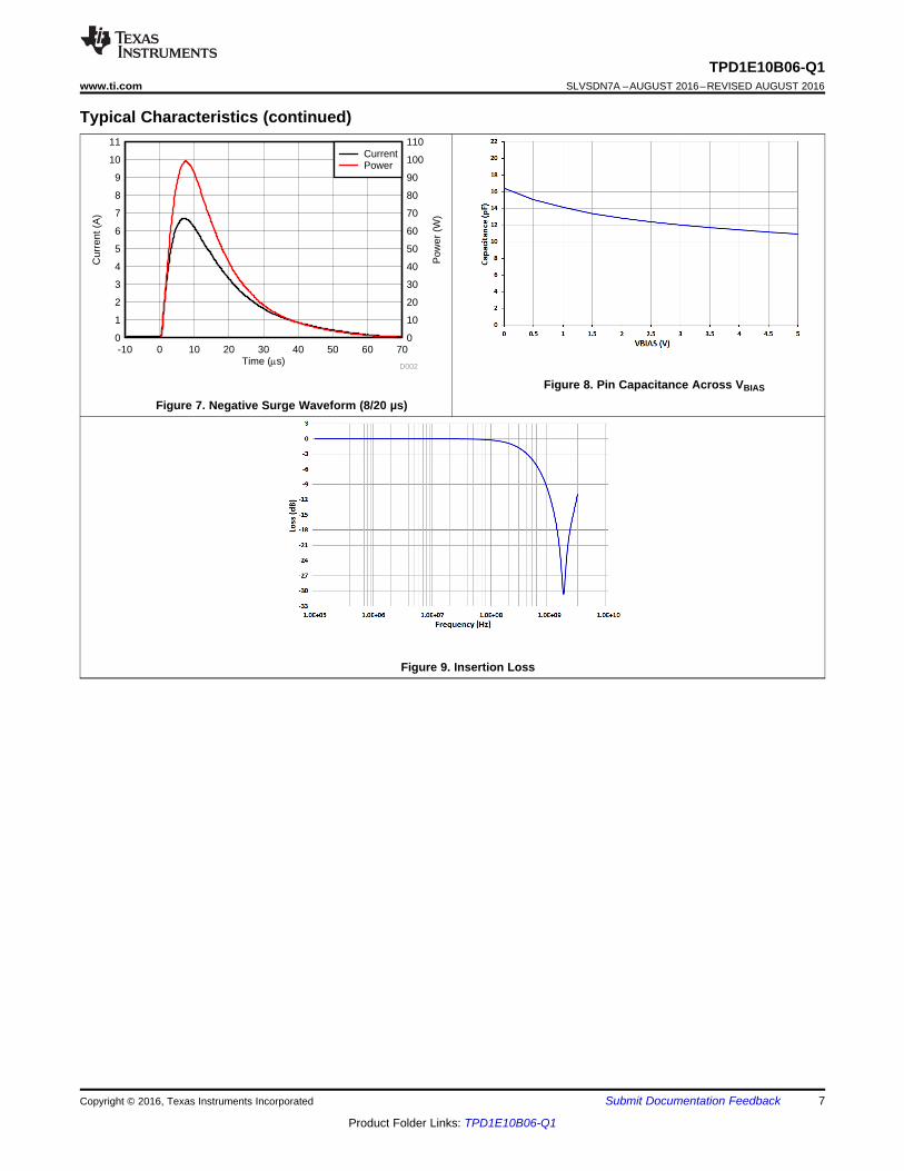
Typical Characteristics (continued)
Figure 7. Negative Surge Waveform (8/20 µs)
Figure 8. Pin Capacitance Across VBIAS
Figure 9. Insertion Loss
1
2
Copyright © 2016, Texas Instruments Incorporated
8
TPD1E10B06-Q1SLVSDN7A –AUGUST 2016–REVISED AUGUST 2016 www.ti.com
Product Folder Links: TPD1E10B06-Q1
Submit Documentation Feedback Copyright © 2016, Texas Instruments Incorporated
7 Detailed Description
7.1 OverviewThe TPD1E10B06-Q1 is a single-channel ESD TVS diode in a small 0402 package. This TVS protection productoffers ±30-kV IEC air-gap, ±30-kV contact ESD protection, and has an ESD clamp circuit with a back-to-backTVS diode for bipolar or bidirectional signal support. The 12-pF line capacitance of this ESD protection diode issuitable for a wide range of applications supporting data rates up to 400 Mbps. The 0402 package is an industrystandard and is convenient for component placement in space-saving applications.
Typical application of this ESD protection product is the circuit protection for audio lines, push buttons, memoryinterfaces, and general-purpose I/O ports. This ESD clamp is a good fit for the protection of the end equipmentssuch as head units, premium audio, external amplifiers, and many other automotive applications.
7.2 Functional Block Diagram
7.3 Feature DescriptionThe TPD1E10B06-Q1 is a bidirectional TVS with high ESD protection level. This device protects circuit from ESDstrikes up to ±30-kV contact and ±30-kV air-gap specified in the IEC 61000-4-2 level 4 international standard.The device can also handle up to 6-A surge current (IEC 61000-4-5 8/20µs). The I/O capacitance of 12 pFsupports a data rate up to 400 Mbps. This clamping device has a small dynamic resistance, which makes theclamping voltage low when the device is actively protecting other circuits. For example, the clamping voltage isonly 10 V when the device is taking 1-A transient current. The breakdown is bidirectional so that this protectiondevice is a good fit for GPIO and especially audio lines which carry bidirectional signals. Low leakage allows thediode to conserve power when working below the VRWM. The industrial temperature range of –40°C to +125°Cmakes this ESD device work at extensive temperatures in most environments. The space-saving 0402 packagecan fit into many flexible spaces.
7.3.1 AEC-Q101 QualifiedThis device is qualified to AEC-Q101 standards and is qualified to operate from –40°C to +125°C.
7.3.2 IEC 61000-4-2 ESD ProtectionThe I/O pins can withstand ESD events up to ±30-kV contact and ±30-kV air according to the IEC 61000-4-2standard. An ESD-surge clamp diverts the current to ground.
7.3.3 ISO 10605 ESD ProtectionThe I/O pins can withstand ESD events at least ±8-kV contact and ±15-kV air according to the ISO 10605 (330pF, 330 Ω) standard. An ESD-surge clamp diverts the current to ground.
7.3.4 IEC 61000-4-5 Surge ProtectionThe IO pins can withstand surge events up to 6 A (8/20 µs waveform). An ESD-surge clamp diverts this currentto ground.
7.3.5 IO CapacitanceThe capacitance between the I/O pins 12 pF. This capacitance support data rates up to 400 Mbps.
9
TPD1E10B06-Q1www.ti.com SLVSDN7A –AUGUST 2016–REVISED AUGUST 2016
Product Folder Links: TPD1E10B06-Q1
Submit Documentation FeedbackCopyright © 2016, Texas Instruments Incorporated
Feature Description (continued)7.3.6 Dynamic ResistanceThe IO pins feature an ESD clamp that has a low RDYN of 0.32 Ω (Pin 1 to Pin 2) and 0.38 Ω (Pin 2 to Pin 1)which prevents system damage during ESD events.
7.3.7 DC Breakdown VoltageThe DC breakdown voltage between the IO pins is a minimum of 6 V. This ensures that sensitive equipment isprotected from surges above the reverse standoff voltage of 5.5 V.
7.3.8 Ultra Low Leakage CurrentThe IO pins feature an ultra-low leakage current of 100 nA (maximum) with a bias of 5 V.
7.3.9 Clamping VoltageThe IO pins feature an ESD clamp that is capable of clamping the voltage to 10 V (IPP = 1 A) and 14V (IPP = 5A).
7.3.10 Industrial Temperature RangeThis device features an industrial operating range of –40°C to +125°C
7.3.11 Space-Saving FootprintThis device features a space-saving, industry standard 0402 footprint.
7.4 Device Functional ModesThe TPD1E10B06-Q1 is a passive clamp that has low leakage during normal operation when the voltagebetween pin 1 and pin 2 is below VRWM and activates when the voltage between pin 1 and pin 2 goes above VBR.During IEC ESD events, transient voltages as high as ±30 kV can be clamped between the two pins. When thevoltages on the protected lines fall below the trigger voltage, the device reverts back to the low leakage passivestate.
GND
SpeakerConnector
(Source of ESD) 1 1
22
L Audio IN
Audio AmplifierClass AB
(ESD Sensitive)
R Audio IN
L
R
Audio AmplifierClass AB
(ESD Sensitive)
GND
GND
L Audio
R Audio
Copyright © 2016, Texas Instruments Incorporated
10
TPD1E10B06-Q1SLVSDN7A –AUGUST 2016–REVISED AUGUST 2016 www.ti.com
Product Folder Links: TPD1E10B06-Q1
Submit Documentation Feedback Copyright © 2016, Texas Instruments Incorporated
8 Application and Implementation
NOTEInformation in the following applications sections is not part of the TI componentspecification, and TI does not warrant its accuracy or completeness. TI’s customers areresponsible for determining suitability of components for their purposes. Customers shouldvalidate and test their design implementation to confirm system functionality.
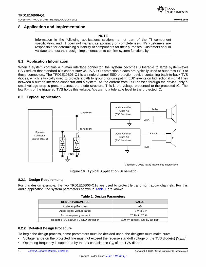
8.1 Application InformationWhen a system contains a human interface connector, the system becomes vulnerable to large system-levelESD strikes that standard ICs cannot survive. TVS ESD protection diodes are typically used to suppress ESD atthese connectors. The TPD1E10B06-Q1 is a single-channel ESD protection device containing back-to-back TVSdiodes, which is typically used to provide a path to ground for dissipating ESD events on bidirectional signal linesbetween a human interface connector and a system. As the current from ESD passes through the device, only asmall voltage drop is present across the diode structure. This is the voltage presented to the protected IC. Thelow RDYN of the triggered TVS holds this voltage, VCLAMP, to a tolerable level to the protected IC.
8.2 Typical Application
Figure 10. Typical Application Schematic
8.2.1 Design RequirementsFor this design example, the two TPD1E10B06-Q1s are used to protect left and right audio channels. For thisaudio application, the system parameters shown in Table 1 are known.
Table 1. Design ParametersDESIGN PARAMETER VALUE
Audio amplifier class ABAudio signal voltage range –3 V to 3 VAudio frequency content 20 Hz to 20 kHz
Required IEC 61000-4-2 ESD protection ±20-kV contact, ±25-kV air-gap
8.2.2 Detailed Design ProcedureTo begin the design process, some parameters must be decided upon; the designer must make sure:• Voltage range on the protected line must not exceed the reverse standoff voltage of the TVS diode(s) (VRWM)• Operating frequency is supported by the I/O capacitance CIO of the TVS diode
11
TPD1E10B06-Q1www.ti.com SLVSDN7A –AUGUST 2016–REVISED AUGUST 2016
Product Folder Links: TPD1E10B06-Q1
Submit Documentation FeedbackCopyright © 2016, Texas Instruments Incorporated
• IEC 61000-4-2 protection requirement is covered by the IEC performance of the TVS diode
For this application, the audio signal voltage range is –3 V to 3 V. The VRWM for the TVS is –5.5 V to 5.5 V;therefore, the bidirectional TVS does not break down during normal operation, and therefore normal operation ofthe audio signal is not effected because of the signal voltage range. In this application, a bidirectional TVS likeTPD1E10B06-Q1 is required.
Next, consider the frequency content of this audio signal. In this application with the class AB amplifier, thefrequency content is from 20 Hz to 20 kHz; ensure that the TVS I/O capacitance does not distort this signal byfiltering it. With the TPD1E10B06-Q1 typical capacitance of 12 pF, which leads to a typical 3-dB bandwidth of400 MHz, this diode has sufficient bandwidth to pass the audio signal without distorting it.
Finally, the human interface in this application requires above standard Level 4 IEC 61000-4-2 system-level ESDprotection (±20-kV Contact, ±25-kV Air-Gap). A standard TVS cannot survive this level of IEC ESD stress.However, the TPD1E10B06-Q1 can survive at least ±30-kV Contact/ ±30-kV Air-Gap. Therefore, the device canprovide sufficient ESD protection for the interface, even though the requirements are stringent. For any TVSdiode to provide the full range of ESD protection capabilities, as well as to minimize the noise and EMIdisturbances the board will see during ESD events, a system designer must use proper board layout of their TVSESD protection diodes. See the Layout section for instructions on properly laying out TPD1E10B06-Q1.
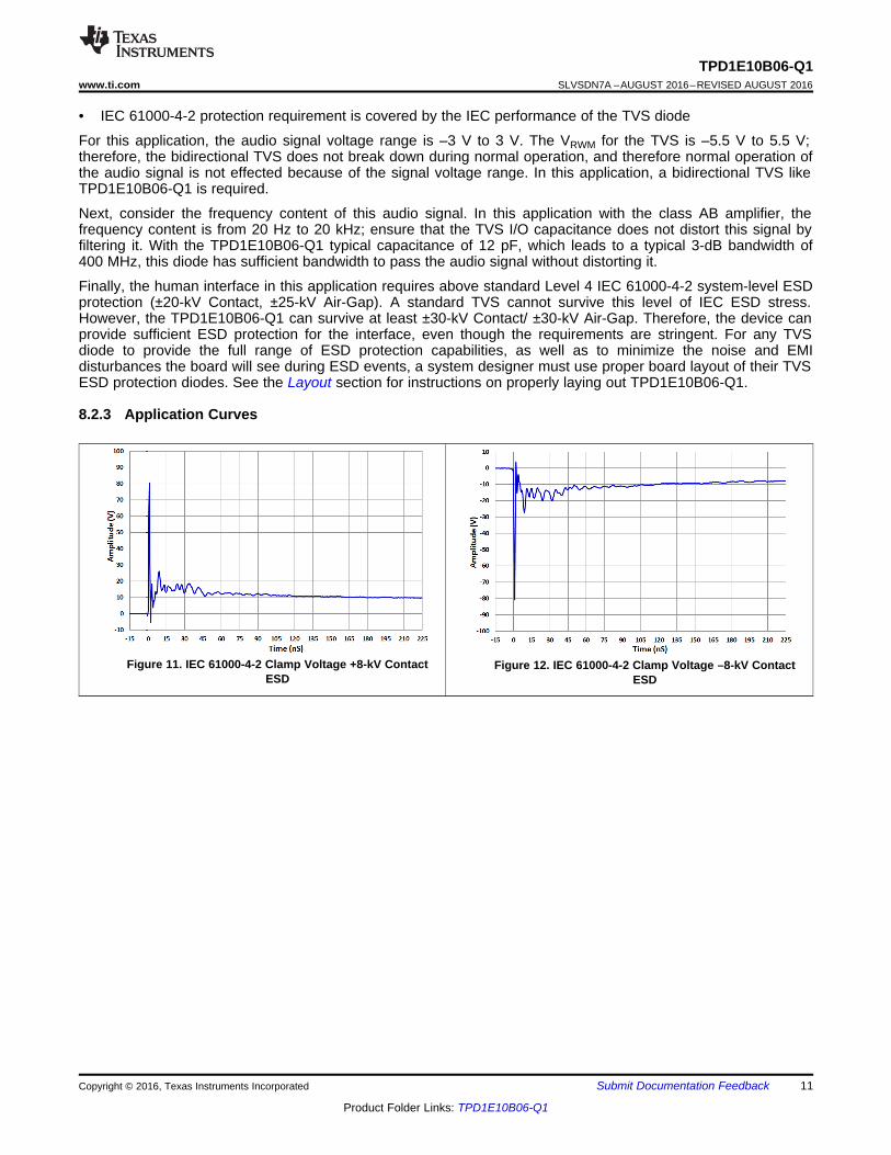
8.2.3 Application Curves
Figure 11. IEC 61000-4-2 Clamp Voltage +8-kV ContactESD
Figure 12. IEC 61000-4-2 Clamp Voltage –8-kV ContactESD
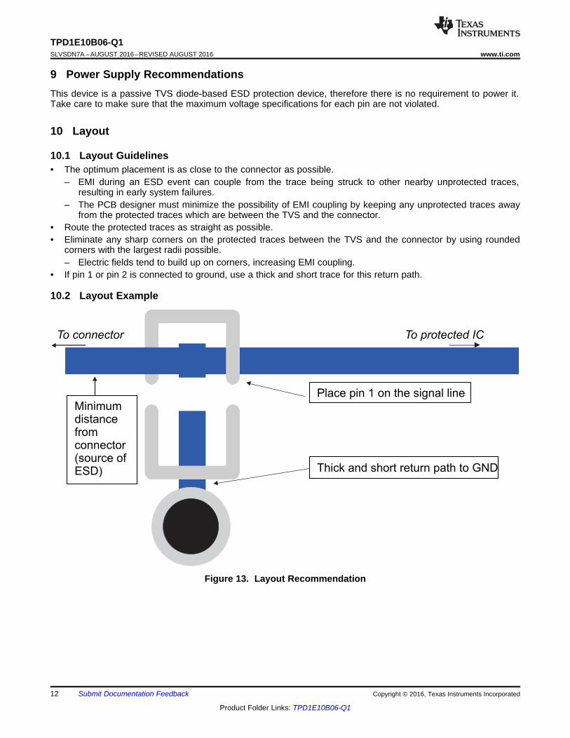
To protected IC
Place pin 1 on the signal line
Thick and short return path to GND
Minimumdistancefromconnector(source ofESD)
To connector
12
TPD1E10B06-Q1SLVSDN7A –AUGUST 2016–REVISED AUGUST 2016 www.ti.com
Product Folder Links: TPD1E10B06-Q1
Submit Documentation Feedback Copyright © 2016, Texas Instruments Incorporated
9 Power Supply RecommendationsThis device is a passive TVS diode-based ESD protection device, therefore there is no requirement to power it.Take care to make sure that the maximum voltage specifications for each pin are not violated.
10 Layout
10.1 Layout Guidelines• The optimum placement is as close to the connector as possible.
– EMI during an ESD event can couple from the trace being struck to other nearby unprotected traces,resulting in early system failures.
– The PCB designer must minimize the possibility of EMI coupling by keeping any unprotected traces awayfrom the protected traces which are between the TVS and the connector.
• Route the protected traces as straight as possible.• Eliminate any sharp corners on the protected traces between the TVS and the connector by using rounded
corners with the largest radii possible.– Electric fields tend to build up on corners, increasing EMI coupling.
• If pin 1 or pin 2 is connected to ground, use a thick and short trace for this return path.
10.2 Layout Example
Figure 13. Layout Recommendation
13
TPD1E10B06-Q1www.ti.com SLVSDN7A –AUGUST 2016–REVISED AUGUST 2016
Product Folder Links: TPD1E10B06-Q1
Submit Documentation FeedbackCopyright © 2016, Texas Instruments Incorporated
11 Device and Documentation Support
11.1 Documentation Support
11.1.1 Related DocumentationFor related documentation see the following:• TPD1E10B06-Q1 Evaluation Module User's Guide• Reading and Understanding an ESD Protection Datasheet• ESD Layout Guide• ESD PROTECTION DIODES EVM
11.2 Receiving Notification of Documentation UpdatesTo receive notification of documentation updates, navigate to the device product folder on ti.com. In the upperright corner, click on Alert me to register and receive a weekly digest of any product information that haschanged. For change details, review the revision history included in any revised document.
11.3 Community ResourcesThe following links connect to TI community resources. Linked contents are provided "AS IS" by the respectivecontributors. They do not constitute TI specifications and do not necessarily reflect TI's views; see TI's Terms ofUse.
TI E2E™ Online Community TI's Engineer-to-Engineer (E2E) Community. Created to foster collaborationamong engineers. At e2e.ti.com, you can ask questions, share knowledge, explore ideas and helpsolve problems with fellow engineers.
Design Support TI's Design Support Quickly find helpful E2E forums along with design support tools andcontact information for technical support.
11.4 TrademarksE2E is a trademark of Texas Instruments.All other trademarks are the property of their respective owners.
11.5 Electrostatic Discharge CautionThis integrated circuit can be damaged by ESD. Texas Instruments recommends that all integrated circuits be handled withappropriate precautions. Failure to observe proper handling and installation procedures can cause damage.
ESD damage can range from subtle performance degradation to complete device failure. Precision integrated circuits may be moresusceptible to damage because very small parametric changes could cause the device not to meet its published specifications.
11.6 GlossarySLYZ022 — TI Glossary.
This glossary lists and explains terms, acronyms, and definitions.
14
TPD1E10B06-Q1SLVSDN7A –AUGUST 2016–REVISED AUGUST 2016 www.ti.com
Product Folder Links: TPD1E10B06-Q1
Submit Documentation Feedback Copyright © 2016, Texas Instruments Incorporated
12 Mechanical, Packaging, and Orderable InformationThe following pages include mechanical, packaging, and orderable information. This information is the mostcurrent data available for the designated devices. This data is subject to change without notice and revision ofthis document. For browser-based versions of this data sheet, refer to the left-hand navigation.
PACKAGE OPTION ADDENDUM
www.ti.com 27-Sep-2016
Addendum-Page 1
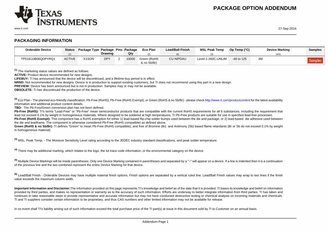
PACKAGING INFORMATION
Orderable Device Status(1)
Package Type PackageDrawing
Pins PackageQty
Eco Plan(2)
Lead/Ball Finish(6)
MSL Peak Temp(3)
Op Temp (°C) Device Marking(4/5)
Samples
TPD1E10B06QDPYRQ1 ACTIVE X1SON DPY 2 10000 Green (RoHS& no Sb/Br)
CU NIPDAU Level-1-260C-UNLIM -40 to 125 4M
(1) The marketing status values are defined as follows:ACTIVE: Product device recommended for new designs.LIFEBUY: TI has announced that the device will be discontinued, and a lifetime-buy period is in effect.NRND: Not recommended for new designs. Device is in production to support existing customers, but TI does not recommend using this part in a new design.PREVIEW: Device has been announced but is not in production. Samples may or may not be available.OBSOLETE: TI has discontinued the production of the device.
(2) Eco Plan - The planned eco-friendly classification: Pb-Free (RoHS), Pb-Free (RoHS Exempt), or Green (RoHS & no Sb/Br) - please check http://www.ti.com/productcontent for the latest availabilityinformation and additional product content details.TBD: The Pb-Free/Green conversion plan has not been defined.Pb-Free (RoHS): TI's terms "Lead-Free" or "Pb-Free" mean semiconductor products that are compatible with the current RoHS requirements for all 6 substances, including the requirement thatlead not exceed 0.1% by weight in homogeneous materials. Where designed to be soldered at high temperatures, TI Pb-Free products are suitable for use in specified lead-free processes.Pb-Free (RoHS Exempt): This component has a RoHS exemption for either 1) lead-based flip-chip solder bumps used between the die and package, or 2) lead-based die adhesive used betweenthe die and leadframe. The component is otherwise considered Pb-Free (RoHS compatible) as defined above.Green (RoHS & no Sb/Br): TI defines "Green" to mean Pb-Free (RoHS compatible), and free of Bromine (Br) and Antimony (Sb) based flame retardants (Br or Sb do not exceed 0.1% by weightin homogeneous material)
(3) MSL, Peak Temp. - The Moisture Sensitivity Level rating according to the JEDEC industry standard classifications, and peak solder temperature.
(4) There may be additional marking, which relates to the logo, the lot trace code information, or the environmental category on the device.
(5) Multiple Device Markings will be inside parentheses. Only one Device Marking contained in parentheses and separated by a "~" will appear on a device. If a line is indented then it is a continuationof the previous line and the two combined represent the entire Device Marking for that device.
(6) Lead/Ball Finish - Orderable Devices may have multiple material finish options. Finish options are separated by a vertical ruled line. Lead/Ball Finish values may wrap to two lines if the finishvalue exceeds the maximum column width.
Important Information and Disclaimer:The information provided on this page represents TI's knowledge and belief as of the date that it is provided. TI bases its knowledge and belief on informationprovided by third parties, and makes no representation or warranty as to the accuracy of such information. Efforts are underway to better integrate information from third parties. TI has taken andcontinues to take reasonable steps to provide representative and accurate information but may not have conducted destructive testing or chemical analysis on incoming materials and chemicals.TI and TI suppliers consider certain information to be proprietary, and thus CAS numbers and other limited information may not be available for release.
In no event shall TI's liability arising out of such information exceed the total purchase price of the TI part(s) at issue in this document sold by TI to Customer on an annual basis.
PACKAGE OPTION ADDENDUM
www.ti.com 27-Sep-2016
Addendum-Page 2
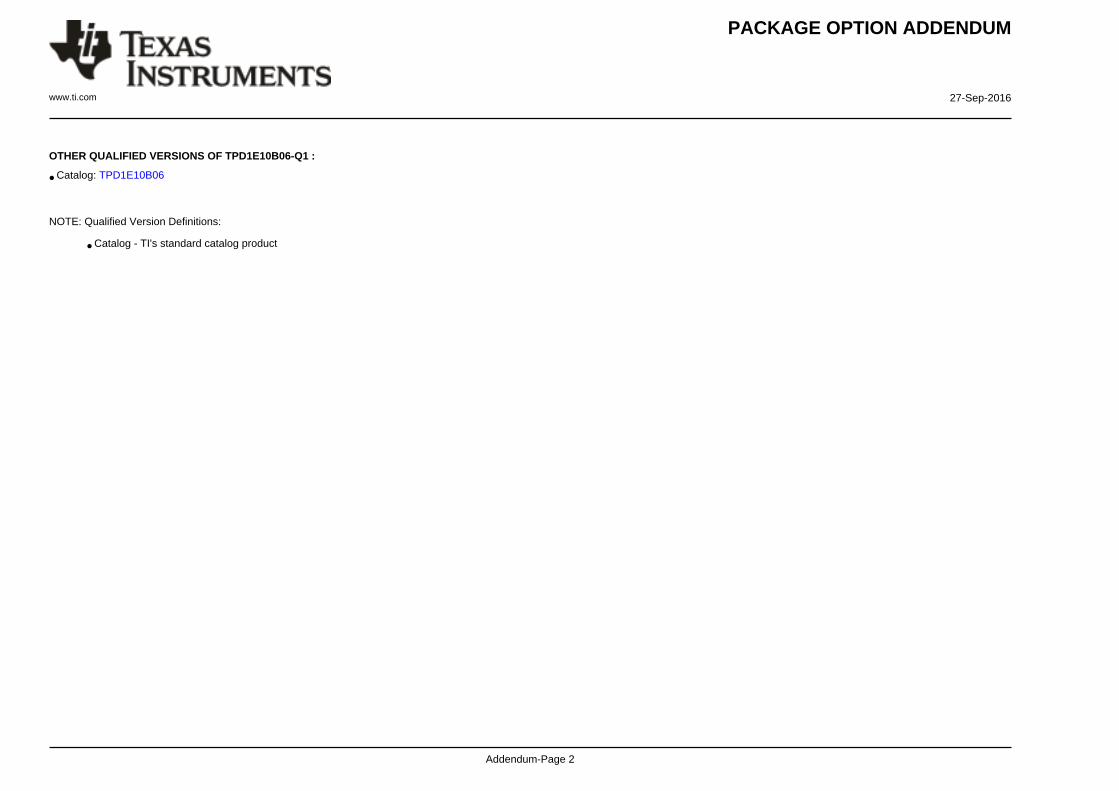
OTHER QUALIFIED VERSIONS OF TPD1E10B06-Q1 :
• Catalog: TPD1E10B06
NOTE: Qualified Version Definitions:
• Catalog - TI's standard catalog product
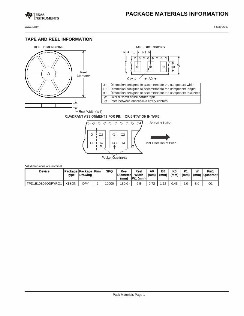
TAPE AND REEL INFORMATION
*All dimensions are nominal
Device PackageType
PackageDrawing
Pins SPQ ReelDiameter
(mm)
ReelWidth
W1 (mm)
A0(mm)
B0(mm)
K0(mm)
P1(mm)
W(mm)
Pin1Quadrant
TPD1E10B06QDPYRQ1 X1SON DPY 2 10000 180.0 9.5 0.72 1.12 0.43 2.0 8.0 Q1
PACKAGE MATERIALS INFORMATION
www.ti.com 6-May-2017
Pack Materials-Page 1
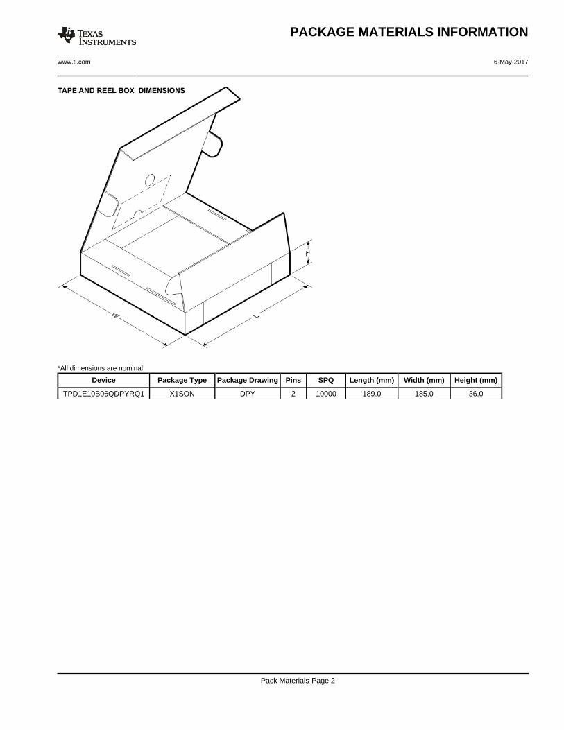
*All dimensions are nominal
Device Package Type Package Drawing Pins SPQ Length (mm) Width (mm) Height (mm)
TPD1E10B06QDPYRQ1 X1SON DPY 2 10000 189.0 185.0 36.0
PACKAGE MATERIALS INFORMATION
www.ti.com 6-May-2017
Pack Materials-Page 2
IMPORTANT NOTICE
Texas Instruments Incorporated (TI) reserves the right to make corrections, enhancements, improvements and other changes to itssemiconductor products and services per JESD46, latest issue, and to discontinue any product or service per JESD48, latest issue. Buyersshould obtain the latest relevant information before placing orders and should verify that such information is current and complete.TI’s published terms of sale for semiconductor products (http://www.ti.com/sc/docs/stdterms.htm) apply to the sale of packaged integratedcircuit products that TI has qualified and released to market. Additional terms may apply to the use or sale of other types of TI products andservices.Reproduction of significant portions of TI information in TI data sheets is permissible only if reproduction is without alteration and isaccompanied by all associated warranties, conditions, limitations, and notices. TI is not responsible or liable for such reproduceddocumentation. Information of third parties may be subject to additional restrictions. Resale of TI products or services with statementsdifferent from or beyond the parameters stated by TI for that product or service voids all express and any implied warranties for theassociated TI product or service and is an unfair and deceptive business practice. TI is not responsible or liable for any such statements.Buyers and others who are developing systems that incorporate TI products (collectively, “Designers”) understand and agree that Designersremain responsible for using their independent analysis, evaluation and judgment in designing their applications and that Designers havefull and exclusive responsibility to assure the safety of Designers' applications and compliance of their applications (and of all TI productsused in or for Designers’ applications) with all applicable regulations, laws and other applicable requirements. Designer represents that, withrespect to their applications, Designer has all the necessary expertise to create and implement safeguards that (1) anticipate dangerousconsequences of failures, (2) monitor failures and their consequences, and (3) lessen the likelihood of failures that might cause harm andtake appropriate actions. Designer agrees that prior to using or distributing any applications that include TI products, Designer willthoroughly test such applications and the functionality of such TI products as used in such applications.TI’s provision of technical, application or other design advice, quality characterization, reliability data or other services or information,including, but not limited to, reference designs and materials relating to evaluation modules, (collectively, “TI Resources”) are intended toassist designers who are developing applications that incorporate TI products; by downloading, accessing or using TI Resources in anyway, Designer (individually or, if Designer is acting on behalf of a company, Designer’s company) agrees to use any particular TI Resourcesolely for this purpose and subject to the terms of this Notice.TI’s provision of TI Resources does not expand or otherwise alter TI’s applicable published warranties or warranty disclaimers for TIproducts, and no additional obligations or liabilities arise from TI providing such TI Resources. TI reserves the right to make corrections,enhancements, improvements and other changes to its TI Resources. TI has not conducted any testing other than that specificallydescribed in the published documentation for a particular TI Resource.Designer is authorized to use, copy and modify any individual TI Resource only in connection with the development of applications thatinclude the TI product(s) identified in such TI Resource. NO OTHER LICENSE, EXPRESS OR IMPLIED, BY ESTOPPEL OR OTHERWISETO ANY OTHER TI INTELLECTUAL PROPERTY RIGHT, AND NO LICENSE TO ANY TECHNOLOGY OR INTELLECTUAL PROPERTYRIGHT OF TI OR ANY THIRD PARTY IS GRANTED HEREIN, including but not limited to any patent right, copyright, mask work right, orother intellectual property right relating to any combination, machine, or process in which TI products or services are used. Informationregarding or referencing third-party products or services does not constitute a license to use such products or services, or a warranty orendorsement thereof. Use of TI Resources may require a license from a third party under the patents or other intellectual property of thethird party, or a license from TI under the patents or other intellectual property of TI.TI RESOURCES ARE PROVIDED “AS IS” AND WITH ALL FAULTS. TI DISCLAIMS ALL OTHER WARRANTIES ORREPRESENTATIONS, EXPRESS OR IMPLIED, REGARDING RESOURCES OR USE THEREOF, INCLUDING BUT NOT LIMITED TOACCURACY OR COMPLETENESS, TITLE, ANY EPIDEMIC FAILURE WARRANTY AND ANY IMPLIED WARRANTIES OFMERCHANTABILITY, FITNESS FOR A PARTICULAR PURPOSE, AND NON-INFRINGEMENT OF ANY THIRD PARTY INTELLECTUALPROPERTY RIGHTS. TI SHALL NOT BE LIABLE FOR AND SHALL NOT DEFEND OR INDEMNIFY DESIGNER AGAINST ANY CLAIM,INCLUDING BUT NOT LIMITED TO ANY INFRINGEMENT CLAIM THAT RELATES TO OR IS BASED ON ANY COMBINATION OFPRODUCTS EVEN IF DESCRIBED IN TI RESOURCES OR OTHERWISE. IN NO EVENT SHALL TI BE LIABLE FOR ANY ACTUAL,DIRECT, SPECIAL, COLLATERAL, INDIRECT, PUNITIVE, INCIDENTAL, CONSEQUENTIAL OR EXEMPLARY DAMAGES INCONNECTION WITH OR ARISING OUT OF TI RESOURCES OR USE THEREOF, AND REGARDLESS OF WHETHER TI HAS BEENADVISED OF THE POSSIBILITY OF SUCH DAMAGES.Unless TI has explicitly designated an individual product as meeting the requirements of a particular industry standard (e.g., ISO/TS 16949and ISO 26262), TI is not responsible for any failure to meet such industry standard requirements.Where TI specifically promotes products as facilitating functional safety or as compliant with industry functional safety standards, suchproducts are intended to help enable customers to design and create their own applications that meet applicable functional safety standardsand requirements. Using products in an application does not by itself establish any safety features in the application. Designers mustensure compliance with safety-related requirements and standards applicable to their applications. Designer may not use any TI products inlife-critical medical equipment unless authorized officers of the parties have executed a special contract specifically governing such use.Life-critical medical equipment is medical equipment where failure of such equipment would cause serious bodily injury or death (e.g., lifesupport, pacemakers, defibrillators, heart pumps, neurostimulators, and implantables). Such equipment includes, without limitation, allmedical devices identified by the U.S. Food and Drug Administration as Class III devices and equivalent classifications outside the U.S.TI may expressly designate certain products as completing a particular qualification (e.g., Q100, Military Grade, or Enhanced Product).Designers agree that it has the necessary expertise to select the product with the appropriate qualification designation for their applicationsand that proper product selection is at Designers’ own risk. Designers are solely responsible for compliance with all legal and regulatoryrequirements in connection with such selection.Designer will fully indemnify TI and its representatives against any damages, costs, losses, and/or liabilities arising out of Designer’s non-compliance with the terms and provisions of this Notice.
Mailing Address: Texas Instruments, Post Office Box 655303, Dallas, Texas 75265Copyright © 2017, Texas Instruments Incorporated