Embed Size (px)
Citation preview
User's GuideSLOU208–August 2007
TPA3123D2 Audio Power Amplifier EVM
Contents1 Introduction ................................................................................................................... 22 Operation ..................................................................................................................... 43 TPA3123D2 EVM Schematic............................................................................................... 54 TPA3123D2 EVM PCB Layers............................................................................................. 65 TPA3123D2 Evaluation Module Parts List ............................................................................... 8
List of Figures
1 TPA3123D2 Audio Power Amplifier EVM (Top View)................................................................... 22 TPA3123D2 Audio Power Amplifier EVM (Bottom View)............................................................... 33 TPA3123D2 EVM Schematic............................................................................................... 54 Top Side Layout.............................................................................................................. 65 Bottom Side Layout.......................................................................................................... 7
List of Tables
1 TPA3123D2 EVM Specifications .......................................................................................... 22 Gain Settings ................................................................................................................. 43 TPA3123D2 EVM Bill of Materials......................................................................................... 8
SLOU208–August 2007 TPA3123D2 Audio Power Amplifier EVM 1Submit Documentation Feedback
www.ti.com
1 Introduction
Introduction
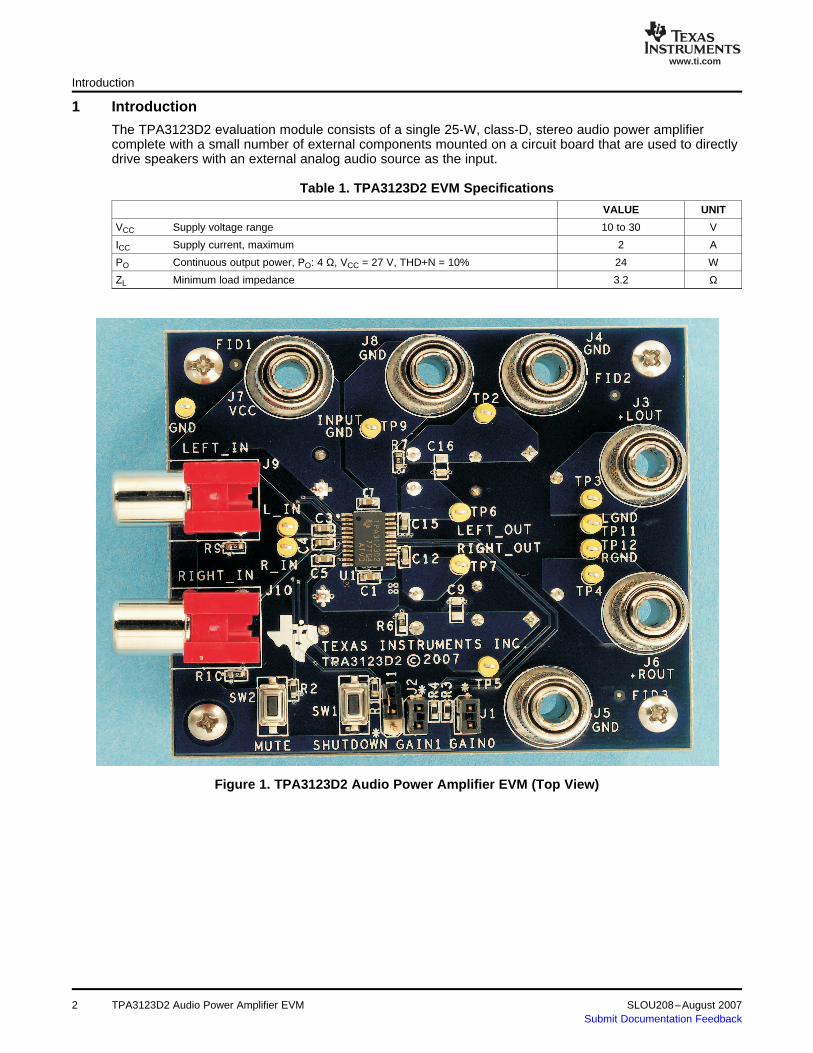
The TPA3123D2 evaluation module consists of a single 25-W, class-D, stereo audio power amplifiercomplete with a small number of external components mounted on a circuit board that are used to directlydrive speakers with an external analog audio source as the input.
Table 1. TPA3123D2 EVM Specifications
VALUE UNIT
VCC Supply voltage range 10 to 30 V
ICC Supply current, maximum 2 A
PO Continuous output power, PO: 4 Ω, VCC = 27 V, THD+N = 10% 24 W
ZL Minimum load impedance 3.2 Ω
Figure 1. TPA3123D2 Audio Power Amplifier EVM (Top View)
2 TPA3123D2 Audio Power Amplifier EVM SLOU208–August 2007Submit Documentation Feedback
www.ti.com
Introduction
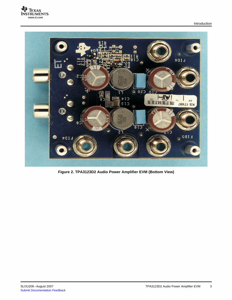
Figure 2. TPA3123D2 Audio Power Amplifier EVM (Bottom View)
SLOU208–August 2007 TPA3123D2 Audio Power Amplifier EVM 3Submit Documentation Feedback
www.ti.com
2 Operation
2.1 Quick Start List for Stand-Alone Operation
2.1.1 Power Supply
2.1.2 Evaluation Module Preparations
Operation
Follow these steps to use the TPA3123D2EVM stand-alone or when connecting it into existing circuits orequipment. Connections to the EVM module can be made by inserting stripped wire, or using bananaplugs for the power supply and output connections. The inputs accept standard RCA plugs.
1. Ensure that all external power sources are set to OFF.2. Connect an external regulated power supply adjusted from 10 V to 30 V to the module VCC (J7) and
GND (J8) banana jacks taking care to observe marked polarity.
Inputs and Outputs:
1. Connect an audio source to the input jacks, J9 and J10.2. Connect a speaker across GND (J5) and +ROUT (J6). Connect another speaker across LOUT (J3)
and GND (J4)3. Install both gain jumpers GAIN0 (J1) and GAIN1 (J2). This sets the gain of the amplifier to the lowest
level, 20 dB.
Control Inputs:
1. SHUTDOWN: This terminal is active LOW. A LOW on the device terminal (<0.8 V) shuts down theamplifier; a HIGH (>2 V) on the device terminal places the amplifier in the active state. Holding downswitch SW1 places the amplifier in the SHUTDOWN state. Releasing SW1 returns the amplifier to theactive state. This terminal is VCC compliant.
2. MUTE: This terminal is active HIGH. A HIGH (>2 V) on this terminal will immediately terminate audioplayback through the speakers; a LOW (<0.8 V) enables the device. The outputs remain switching withfifty percent duty cycle. SW2 on the EVM controls the state of the MUTE terminal. Holding down switchSW2 places the amplifier in the MUTE state. Releasing SW2 returns the amplifier to the active state.This terminal is VCC compliant.
3. GAIN0/GAIN1: Together, these terminals determine the gain of the amplifier. See Table 2. Installing ajumper in J1 or J2 sets the respective terminal to GND. Removing the jumper sets the respectiveterminals to VCC. Removing jumpers increases the gain while installing jumpers decreases the gain.Logic levels are TTL compatible. These terminals are VCC compliant.
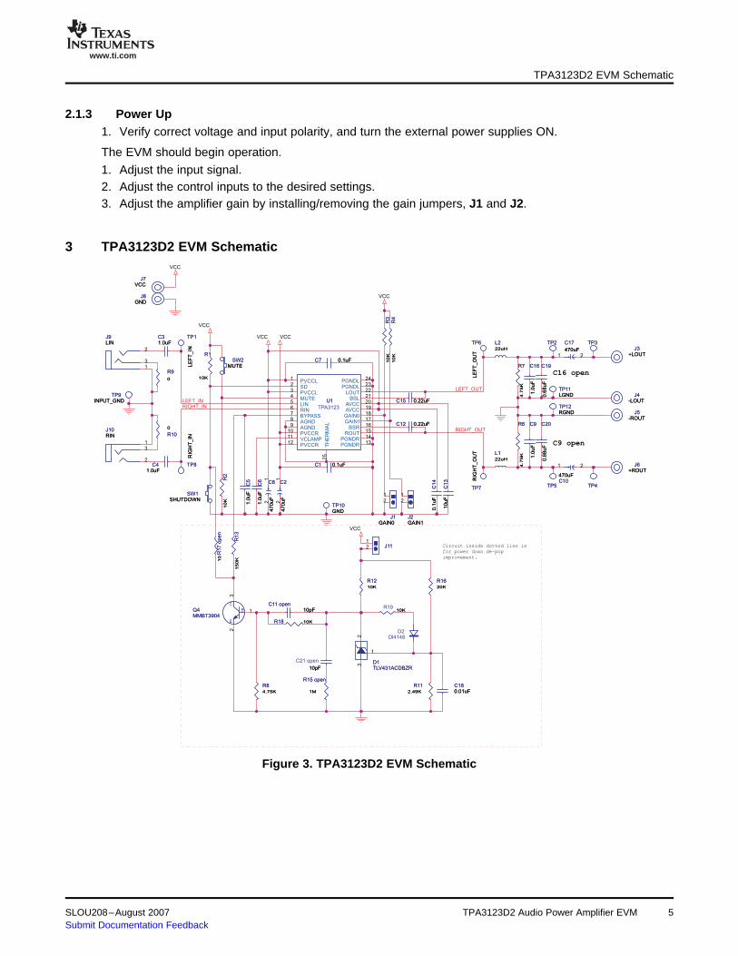
4. Power-off Depop Circuit: Additional circuitry to quiet power-off pop is provided on the EVM. Thiscircuit consists of shunt regulator D1, bipolar transistor Q4, and the surrounding components. Thiscircuit is activated by installing the jumper J11 which connects VCC to the network. The depop circuithas two different modes of operation. When R13 is installed, this circuit slowly pulls down the voltageon the Bypass pin when power is removed resulting in a controlled reduction of the Class D outputduty cycle. If R17 is installed, the network reduces the pop by pulling down the shutdown pin atpower-off. This approach can be used if the power supply operates in such a way that there is asignificant time delay between removal of power and the point where VCC falls below the chip UVLOlevel, which is approximately 8 volts.
Table 2. Gain Settings
GAIN0 (J1) GAIN1 (J2) Amplifier Gain (dB)
ON ON 20
ON OFF 26
OFF ON 32
OFF OFF 36
TPA3123D2 Audio Power Amplifier EVM4 SLOU208–August 2007Submit Documentation Feedback
www.ti.com
2.1.3 Power Up
3 TPA3123D2 EVM Schematic
RIGHT_OUT
LEFT_INRIGHT_IN
LEFT_OUT
VCC
VCC
VCC
VCC
VCC
VCC
C9 open
C16 open
Circuit inside dotted line is
for power down de-pop
improvement.
R3
10
KR
31
0K
J4-LOUT
J4-LOUT
TP4TP4
SW1SHUTDOWN
SW1SHUTDOWN
U1U1
TPA3123
PVCCL1
SD2
PVCCL3
MUTE4
LIN5
RIN6
BYPASS7
AGND8
AGND9
PVCCR10
VCLAMP11
PVCCR12 PGNDR 13
PGNDR 14ROUT 15
BSR 16GAIN1 17GAIN0 18AVCC 19AVCC 20
BSL 21LOUT 22
PGNDL 23PGNDL 24
TH
ER
MA
L25
C14
0.1
uF
C14
0.1
uF
TP5TP5
R6
4.7
5K
R6
4.7
5K
L222uH
L222uH
J7VCC
J7VCC
R1210K
R1210K
C6
1.0
uF
C6
1.0
uF
R9
0
R9
0
D2Dl4148
R4
10
KR
41
0K
C180.01uFC180.01uF
R17
open
10
R17
open
10
TP12RGNDTP12RGND
SW2MUTE
SW2MUTE
TP3TP3
C12 0.22uFC12 0.22uF C9
1.0
uF
C9
1.0
uF
R1620K
R1620K
R7
4.7
5K
R7
4.7
5K
+
C8
470uF
+
C8
470uF
12
J8GND
J8GND
TP2TP2
J10RINJ10RIN
2
31
R84.75K
R84.75K
J9LINJ9LIN
2
31
R18 10KR18 10K
+
C10470uF
+
C10470uF
1 2
J11J1112
TP10GNDTP10GND
C16
1.0
uF
C16
1.0
uF
R1
10K
R1
10K
C15 0.22uFC15 0.22uF
R13
15
0K
R13
15
0K
TP7
RIG
HT
_O
UT
TP7
RIG
HT
_O
UT
J5-ROUT
J5-ROUT
J1GAIN0
J1GAIN0
12
+
C17
470uF
+
C17
470uF1 2
C31.0uFC31.0uF
R15 open
1M
R15 open
1M
J3+LOUT
J3+LOUT
TP11LGNDTP11LGND
TP1
LE
FT
_IN
TP1
LE
FT
_IN
C19
0.6
8uF
C19
0.6
8uF
R2
10
KR
21
0K
C
E
BQ4MMBT3904
C
E
BQ4MMBT3904
1
23
+
C2
470uF
+
C2
470uF
12
J6+ROUT
J6+ROUT
R10
0
R10
0
C11 open10pF
C11 open10pF
10pF
C21 open
10pF
C13
10uF
C13
10uF
C41.0uF
C41.0uF
J2GAIN1J2GAIN1
12
C7 0.1uFC7 0.1uF
C20
0.6
8uF
C20
0.6
8uF
TP6
LE
FT
_O
UT
TP6
LE
FT
_O
UT
R112.49K
R112.49K
10KR19
10K
D1TLV431ACDBZRD1TLV431ACDBZR
32
1
C1 0.1uFC1 0.1uF
TP9INPUT_GND
TP9INPUT_GND
TP8
RIG
HT
_IN
TP8
RIG
HT
_IN
L122uH
L122uH
C5
1.0
uF
C5
1.0
uF
TPA3123D2 EVM Schematic
1. Verify correct voltage and input polarity, and turn the external power supplies ON.
The EVM should begin operation.
1. Adjust the input signal.2. Adjust the control inputs to the desired settings.3. Adjust the amplifier gain by installing/removing the gain jumpers, J1 and J2.
Figure 3. TPA3123D2 EVM Schematic
SLOU208–August 2007 TPA3123D2 Audio Power Amplifier EVM 5Submit Documentation Feedback
www.ti.com
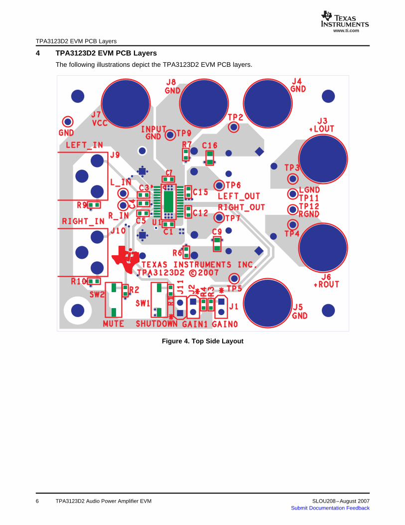
4 TPA3123D2 EVM PCB Layers
3
TPA3123D2 EVM PCB Layers
The following illustrations depict the TPA3123D2 EVM PCB layers.
Figure 4. Top Side Layout
6 TPA3123D2 Audio Power Amplifier EVM SLOU208–August 2007Submit Documentation Feedback
www.ti.com
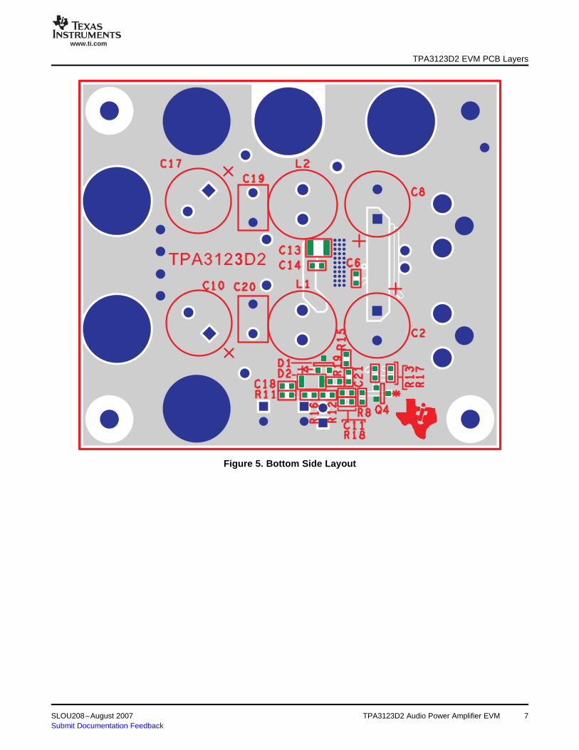
3
TPA3123D2 EVM PCB Layers
Figure 5. Bottom Side Layout
SLOU208–August 2007 TPA3123D2 Audio Power Amplifier EVM 7Submit Documentation Feedback
www.ti.com
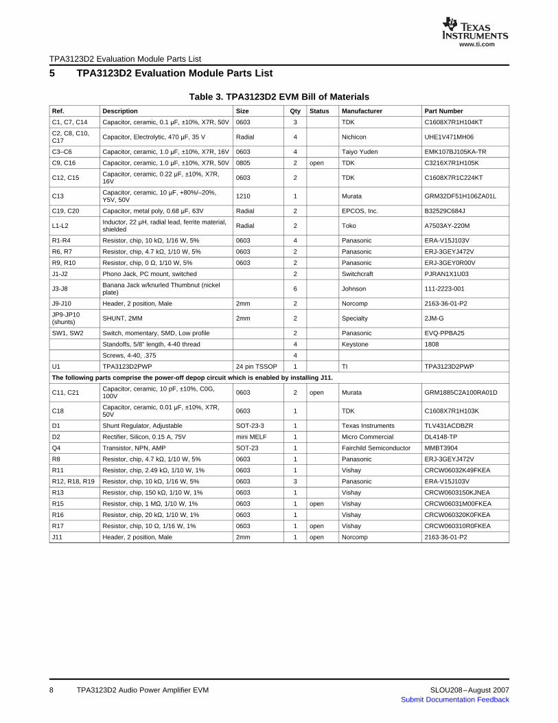
5 TPA3123D2 Evaluation Module Parts ListTPA3123D2 Evaluation Module Parts List
Table 3. TPA3123D2 EVM Bill of MaterialsRef. Description Size Qty Status Manufacturer Part Number
C1, C7, C14 Capacitor, ceramic, 0.1 μF, ±10%, X7R, 50V 0603 3 TDK C1608X7R1H104KT
C2, C8, C10, Capacitor, Electrolytic, 470 μF, 35 V Radial 4 Nichicon UHE1V471MH06C17
C3–C6 Capacitor, ceramic, 1.0 μF, ±10%, X7R, 16V 0603 4 Taiyo Yuden EMK107BJ105KA-TR
C9, C16 Capacitor, ceramic, 1.0 μF, ±10%, X7R, 50V 0805 2 open TDK C3216X7R1H105K
Capacitor, ceramic, 0.22 μF, ±10%, X7R,C12, C15 0603 2 TDK C1608X7R1C224KT16V
Capacitor, ceramic, 10 μF, +80%/–20%,C13 1210 1 Murata GRM32DF51H106ZA01LY5V, 50V
C19, C20 Capacitor, metal poly, 0.68 μF, 63V Radial 2 EPCOS, Inc. B32529C684J
Inductor, 22 μH, radial lead, ferrite material,L1-L2 Radial 2 Toko A7503AY-220Mshielded
R1-R4 Resistor, chip, 10 kΩ, 1/16 W, 5% 0603 4 Panasonic ERA-V15J103V
R6, R7 Resistor, chip, 4.7 kΩ, 1/10 W, 5% 0603 2 Panasonic ERJ-3GEYJ472V
R9, R10 Resistor, chip, 0 Ω, 1/10 W, 5% 0603 2 Panasonic ERJ-3GEY0R00V
J1-J2 Phono Jack, PC mount, switched 2 Switchcraft PJRAN1X1U03
Banana Jack w/knurled Thumbnut (nickelJ3-J8 6 Johnson 111-2223-001plate)
J9-J10 Header, 2 position, Male 2mm 2 Norcomp 2163-36-01-P2
JP9-JP10 SHUNT, 2MM 2mm 2 Specialty 2JM-G(shunts)
SW1, SW2 Switch, momentary, SMD, Low profile 2 Panasonic EVQ-PPBA25
Standoffs, 5/8" length, 4-40 thread 4 Keystone 1808
Screws, 4-40, .375 4
U1 TPA3123D2PWP 24 pin TSSOP 1 TI TPA3123D2PWP
The following parts comprise the power-off depop circuit which is enabled by installing J11.
Capacitor, ceramic, 10 pF, ±10%, C0G,C11, C21 0603 2 open Murata GRM1885C2A100RA01D100V
Capacitor, ceramic, 0.01 μF, ±10%, X7R,C18 0603 1 TDK C1608X7R1H103K50V
D1 Shunt Regulator, Adjustable SOT-23-3 1 Texas Instruments TLV431ACDBZR
D2 Rectifier, Silicon, 0.15 A, 75V mini MELF 1 Micro Commercial DL4148-TP
Q4 Transistor, NPN, AMP SOT-23 1 Fairchild Semiconductor MMBT3904
R8 Resistor, chip, 4.7 kΩ, 1/10 W, 5% 0603 1 Panasonic ERJ-3GEYJ472V
R11 Resistor, chip, 2.49 kΩ, 1/10 W, 1% 0603 1 Vishay CRCW06032K49FKEA
R12, R18, R19 Resistor, chip, 10 kΩ, 1/16 W, 5% 0603 3 Panasonic ERA-V15J103V
R13 Resistor, chip, 150 kΩ, 1/10 W, 1% 0603 1 Vishay CRCW0603150KJNEA
R15 Resistor, chip, 1 MΩ, 1/10 W, 1% 0603 1 open Vishay CRCW06031M00FKEA
R16 Resistor, chip, 20 kΩ, 1/10 W, 1% 0603 1 Vishay CRCW060320K0FKEA
R17 Resistor, chip, 10 Ω, 1/16 W, 1% 0603 1 open Vishay CRCW060310R0FKEA
J11 Header, 2 position, Male 2mm 1 open Norcomp 2163-36-01-P2
TPA3123D2 Audio Power Amplifier EVM8 SLOU208–August 2007Submit Documentation Feedback
EVALUATION BOARD/KIT IMPORTANT NOTICE
Texas Instruments (TI) provides the enclosed product(s) under the following conditions:
This evaluation board/kit is intended for use for ENGINEERING DEVELOPMENT, DEMONSTRATION, OR EVALUATION PURPOSESONLY and is not considered by TI to be a finished end-product fit for general consumer use. Persons handling the product(s) must haveelectronics training and observe good engineering practice standards. As such, the goods being provided are not intended to be completein terms of required design-, marketing-, and/or manufacturing-related protective considerations, including product safety and environmentalmeasures typically found in end products that incorporate such semiconductor components or circuit boards. This evaluation board/kit doesnot fall within the scope of the European Union directives regarding electromagnetic compatibility, restricted substances (RoHS), recycling(WEEE), FCC, CE or UL, and therefore may not meet the technical requirements of these directives or other related directives.
Should this evaluation board/kit not meet the specifications indicated in the User’s Guide, the board/kit may be returned within 30 days fromthe date of delivery for a full refund. THE FOREGOING WARRANTY IS THE EXCLUSIVE WARRANTY MADE BY SELLER TO BUYERAND IS IN LIEU OF ALL OTHER WARRANTIES, EXPRESSED, IMPLIED, OR STATUTORY, INCLUDING ANY WARRANTY OFMERCHANTABILITY OR FITNESS FOR ANY PARTICULAR PURPOSE.
The user assumes all responsibility and liability for proper and safe handling of the goods. Further, the user indemnifies TI from all claimsarising from the handling or use of the goods. Due to the open construction of the product, it is the user’s responsibility to take any and allappropriate precautions with regard to electrostatic discharge.
EXCEPT TO THE EXTENT OF THE INDEMNITY SET FORTH ABOVE, NEITHER PARTY SHALL BE LIABLE TO THE OTHER FOR ANYINDIRECT, SPECIAL, INCIDENTAL, OR CONSEQUENTIAL DAMAGES.
TI currently deals with a variety of customers for products, and therefore our arrangement with the user is not exclusive.
TI assumes no liability for applications assistance, customer product design, software performance, or infringement of patents orservices described herein.
Please read the User’s Guide and, specifically, the Warnings and Restrictions notice in the User’s Guide prior to handling the product. Thisnotice contains important safety information about temperatures and voltages. For additional information on TI’s environmental and/orsafety programs, please contact the TI application engineer or visit www.ti.com/esh.
No license is granted under any patent right or other intellectual property right of TI covering or relating to any machine, process, orcombination in which such TI products or services might be or are used.
FCC Warning
This evaluation board/kit is intended for use for ENGINEERING DEVELOPMENT, DEMONSTRATION, OR EVALUATION PURPOSESONLY and is not considered by TI to be a finished end-product fit for general consumer use. It generates, uses, and can radiate radiofrequency energy and has not been tested for compliance with the limits of computing devices pursuant to part 15 of FCC rules, which aredesigned to provide reasonable protection against radio frequency interference. Operation of this equipment in other environments maycause interference with radio communications, in which case the user at his own expense will be required to take whatever measures maybe required to correct this interference.
Mailing Address: Texas Instruments, Post Office Box 655303, Dallas, Texas 75265Copyright 2007, Texas Instruments Incorporated
EVM WARNINGS AND RESTRICTIONS
It is important to operate this EVM within the input voltage range of 10 V to 30 V and the output voltage range of 0 V to 30 V.
Exceeding the specified input range may cause unexpected operation and/or irreversible damage to the EVM. If there are questionsconcerning the input range, please contact a TI field representative prior to connecting the input power.
Applying loads outside of the specified output range may result in unintended operation and/or possible permanent damage to the EVM.Please consult the EVM User's Guide prior to connecting any load to the EVM output. If there is uncertainty as to the load specification,please contact a TI field representative.
During normal operation, some circuit components may have case temperatures greater than 85°C. The EVM is designed to operateproperly with certain components above 85°C as long as the input and output ranges are maintained. These components include but arenot limited to linear regulators, switching transistors, pass transistors, and current sense resistors. These types of devices can be identifiedusing the EVM schematic located in the EVM User's Guide. When placing measurement probes near these devices during operation,please be aware that these devices may be very warm to the touch.
Mailing Address: Texas Instruments, Post Office Box 655303, Dallas, Texas 75265Copyright 2007, Texas Instruments Incorporated
IMPORTANT NOTICE
Texas Instruments Incorporated and its subsidiaries (TI) reserve the right to make corrections, modifications, enhancements,improvements, and other changes to its products and services at any time and to discontinue any product or service without notice.Customers should obtain the latest relevant information before placing orders and should verify that such information is current andcomplete. All products are sold subject to TI’s terms and conditions of sale supplied at the time of order acknowledgment.
TI warrants performance of its hardware products to the specifications applicable at the time of sale in accordance with TI’sstandard warranty. Testing and other quality control techniques are used to the extent TI deems necessary to support thiswarranty. Except where mandated by government requirements, testing of all parameters of each product is not necessarilyperformed.
TI assumes no liability for applications assistance or customer product design. Customers are responsible for their products andapplications using TI components. To minimize the risks associated with customer products and applications, customers shouldprovide adequate design and operating safeguards.
TI does not warrant or represent that any license, either express or implied, is granted under any TI patent right, copyright, maskwork right, or other TI intellectual property right relating to any combination, machine, or process in which TI products or servicesare used. Information published by TI regarding third-party products or services does not constitute a license from TI to use suchproducts or services or a warranty or endorsement thereof. Use of such information may require a license from a third party underthe patents or other intellectual property of the third party, or a license from TI under the patents or other intellectual property of TI.
Reproduction of TI information in TI data books or data sheets is permissible only if reproduction is without alteration and isaccompanied by all associated warranties, conditions, limitations, and notices. Reproduction of this information with alteration is anunfair and deceptive business practice. TI is not responsible or liable for such altered documentation. Information of third partiesmay be subject to additional restrictions.
Resale of TI products or services with statements different from or beyond the parameters stated by TI for that product or servicevoids all express and any implied warranties for the associated TI product or service and is an unfair and deceptive businesspractice. TI is not responsible or liable for any such statements.
TI products are not authorized for use in safety-critical applications (such as life support) where a failure of the TI product wouldreasonably be expected to cause severe personal injury or death, unless officers of the parties have executed an agreementspecifically governing such use. Buyers represent that they have all necessary expertise in the safety and regulatory ramificationsof their applications, and acknowledge and agree that they are solely responsible for all legal, regulatory and safety-relatedrequirements concerning their products and any use of TI products in such safety-critical applications, notwithstanding anyapplications-related information or support that may be provided by TI. Further, Buyers must fully indemnify TI and itsrepresentatives against any damages arising out of the use of TI products in such safety-critical applications.
TI products are neither designed nor intended for use in military/aerospace applications or environments unless the TI products arespecifically designated by TI as military-grade or "enhanced plastic." Only products designated by TI as military-grade meet militaryspecifications. Buyers acknowledge and agree that any such use of TI products which TI has not designated as military-grade issolely at the Buyer's risk, and that they are solely responsible for compliance with all legal and regulatory requirements inconnection with such use.
TI products are neither designed nor intended for use in automotive applications or environments unless the specific TI productsare designated by TI as compliant with ISO/TS 16949 requirements. Buyers acknowledge and agree that, if they use anynon-designated products in automotive applications, TI will not be responsible for any failure to meet such requirements.
Following are URLs where you can obtain information on other Texas Instruments products and application solutions:
Products Applications
Amplifiers amplifier.ti.com Audio www.ti.com/audio
Data Converters dataconverter.ti.com Automotive www.ti.com/automotive
DSP dsp.ti.com Broadband www.ti.com/broadband
Interface interface.ti.com Digital Control www.ti.com/digitalcontrol
Logic logic.ti.com Military www.ti.com/military
Power Mgmt power.ti.com Optical Networking www.ti.com/opticalnetwork
Microcontrollers microcontroller.ti.com Security www.ti.com/security
RFID www.ti-rfid.com Telephony www.ti.com/telephony
Low Power www.ti.com/lpw Video & Imaging www.ti.com/videoWireless
Wireless www.ti.com/wireless
Mailing Address: Texas Instruments, Post Office Box 655303, Dallas, Texas 75265Copyright © 2007, Texas Instruments Incorporated


![OFDM error floor based EVM estimation Error Floor Based EVM Estimation.pdfAWGN source producing the same BER (and EVM) degradation. [1]: The resulting EVM(BER) curves were verified](https://img.pdfslide.us/doc/110x75/5f2e7bc463c3260b31328bb2/ofdm-error-floor-based-evm-estimation-error-floor-based-evm-awgn-source-producing.jpg)