Embed Size (px)
Citation preview
A. Maląg, G. Sobczak, E. Dąbrowska, ...
MATERIAŁY ELEKTRONICZNE (Electronic Materials), T. 43, Nr 3/2015 7
Towards improvement of beam quality of wide-stripe high-power laser diodes
Andrzej Maląg, Grzegorz Sobczak, Elżbieta Dąbrowska, Marian Teodorczyk,
Andrzej Dąbrowski, Magdalena Nakielska Institute of Electronic Materials Technology
ul. Wólczyńska 133, 01 - 919 Warsaw, Poland e-mail: [email protected]
Abstract: Selected ways of improving an emitted beam quality of high-power laser diodes (LDs) are proposed in both vertical and horizontal directions. Appropriate heterostructure design leads to a vertical beam divergence reduction to 12º (FWHM) while simultaneously maintaining a high power conversion efficiency of LDs. In turn, the spatial stabilization of an optical field distribution in the junction plane results in horizontal beam profile stabilization as a function of the device drive current. This spatial stabilization (with preferred high-order lateral modes) is forced by ion-implanted lateral periodicity built into the wide-stripe waveguide of a LD.
Key words: laser diode, laser beam, heterostructure, directional characteristics of emission
Kierunki poprawy jakości wiązki promieniowania szerokopaskowych diod laserowych dużej mocy Streszczenie: Przedstawione zostały wybrane przykłady poprawy jakości wiązki promieniowania diod laserowych (DL) dużej mocy w płaszczyźnie prostopadłej do złącza (pionowej) i w płaszczyźnie złącza (poziomej). Odpowiedni projekt heterostruktury umożliwia ograniczenie rozbieżności wiązki w płaszczyźnie pionowej do 12º przy utrzymaniu wysokiej sprawności energetycznej DL. Z kolei stabilizacja pola optycznego w płaszczyźnie złącza wymuszona przez strukturę periodyczną wbudowaną w szerokopaskowy światłowód heterostruktury laserowej prowadzi do stabilizacji profilu wiązki w płaszczyźnie poziomej w funkcji poziomu wysterowania przyrządu. Ta struktura periodyczna (preferująca wysokie mody boczne) jest formowana techniką implantacji jonów.
Słowa kluczowe: dioda laserowa, wiązka laserowa, heterostruktura, charakterystyki kierunkowe emisji
1. Introduction
Laser diodes (LDs) are one of the key elements in optoelectronics, widely used in the pumping systems of solid state and fiber lasers and also directly in material processing, free space communication, metrology [1 - 5] etc. This is due to their high electrical-to-optical power conversion efficiency and possibility of choosing spectral characteristics for the intended application. However, direct applications in more demanding optical systems such as engraving, printing, etc. are limited. In wide--stripe waveguide constructions, typical for high-power laser diodes, a multimode and multi-filamentary optical field distribution in a cavity is unstable in time and as a function of the drive current, thus making the precise and stable focusing of a highly divergent optical beam impossible [6]. In the case of wide-stripe LDs design the features determining the beam quality in the junction (‘ho-rizontal’) plane and in the direction perpendicular to the junction (‘vertical’) can be distinguished and considered separately. The gain-guiding in the junction plane and the index-guiding in the vertical direction are typical solutions [7 - 9]. This leads to beam astigmatism [10]. Besides this ‘intrinsic’ consequence, the beam properties in either di-rection can be influenced by the individual constituents of
the device designe. In Section 2, the laser heterostructure design aimed at the vertical beam divergence reduction is presented, whereas in Section 3 the way of stabilizing the emitted beam profile in the horizontal plane is proposed by introducing a lateral gain periodicity into the active stripe by ion implantation.
2. Design in the direction perpendicular to the junction plane
The optical field distribution and the resultant direc-tional characteristics of the emitted beam are determined by the heterostructure waveguide profile. If properly de-signed, the waveguide is strong enough to stabilize only the fundamental transverse mode. Therefore, the details of the heterostructure design remain subject to optimization.
Maximizing an attainable optical power (which is the main design objective in high-power LDs) by enlarging the guided mode size results in the reduction of the ver-tical beam divergence. This is beneficial for effectiveness and simplification of the necessary focusing optics. The mode size or (equivalently) the effective heterostructure waveguide thickness deff = d/Γ, where d is the quantum
Towards improvement of beam quality of wide-stripe high-power ...
8 MATERIAŁY ELEKTRONICZNE (Electronic Materials), T. 43, Nr 3/2015
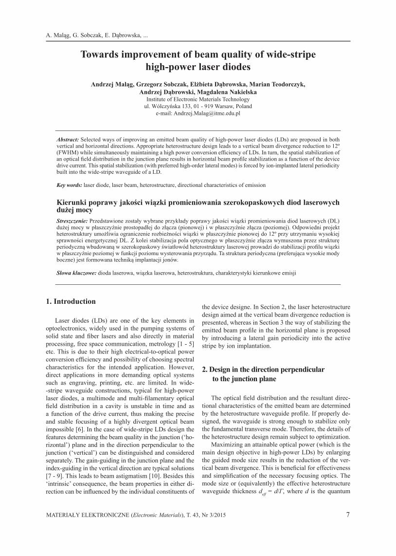
well (QW) thickness and Γ is the QW confinement factor. However the relation between deff and the beam divergence is not straightforward and depends on the heterostructure waveguide design details. It has been proven that in the case of waveguides with similar values of deff decisive for the beam divergence is the optical field profile. Wide evanescent tails penetrating deeply into cladding layers are more crucial for the beam divergence reduction than the mode full width at half maximum (FWHM) [11]. This is illustrated in Fig. 1, showing the refractive index profile and the optical field distribution for the laser double--barrier separated-confinement heterostructure (DBSCH) [12] designed for the 885 nm wavelength range. The wide optical field distribution controlled by thin low-index antiguiding layers inserted between the waveguide and cladding layers results in the record-low vertical beam divergence (VBD) of 12º (FWHM) at deff = 0.97 μm. This is shown in Fig. 2a for CW operation. The LD drive current range measured here is limited by the wear of the filters of the CCD camera used for the far-field recording. The far-field data was corrected with the aid of software for the non-spherical surface of the CCD sensor. The P-I-V characteristics of this LD are shown in Fig. 2b. The threshold current density (Jth), slope efficiency (S) and po-wer-conversion-efficiency (PCE) are 220 Acm-2, 1.1 W/A and 0.55, respectively. The maximum emitted power is 13 W for this slightly compressively strained InGaAs QW LD of the cavity length L = 3 mm and the stripewidth W = 0.18 mm.
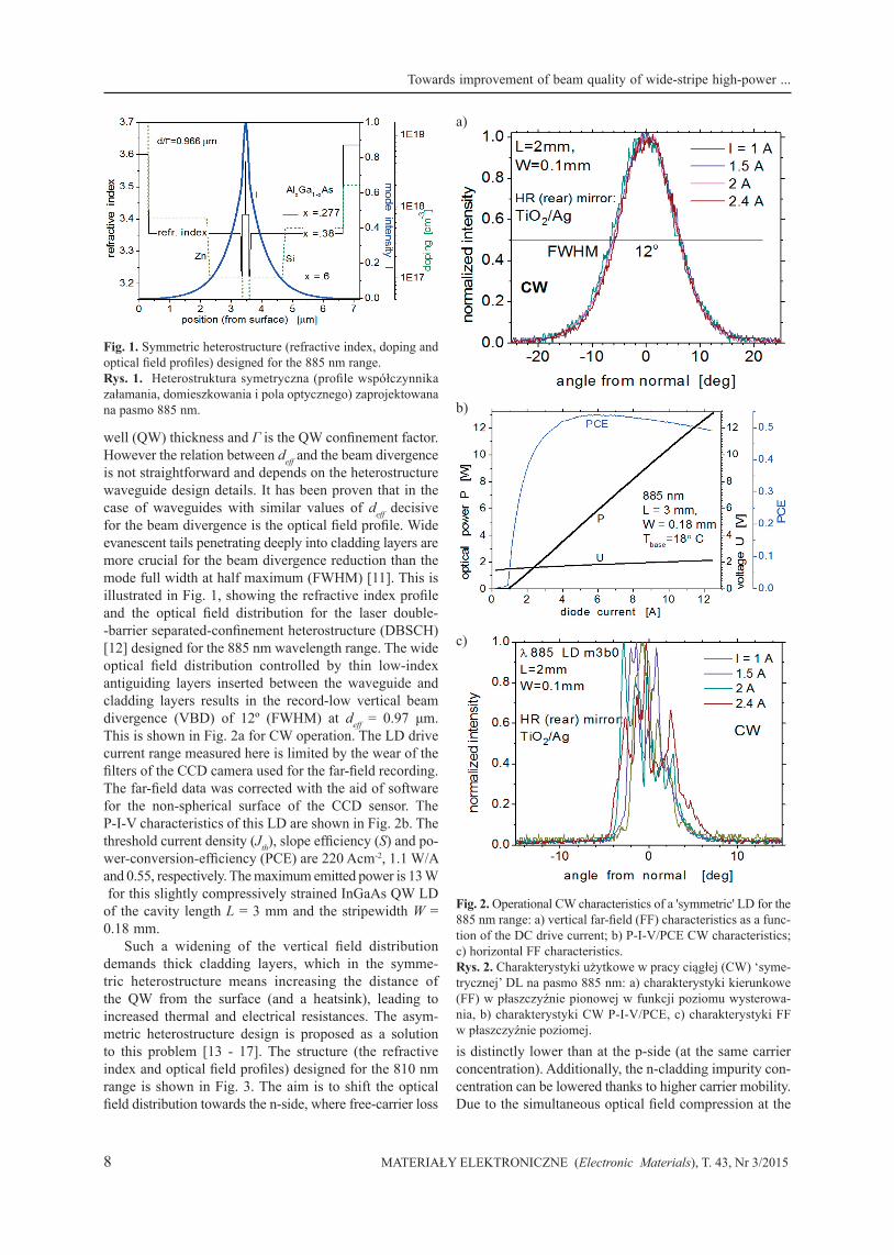
Such a widening of the vertical field distribution demands thick cladding layers, which in the symme-tric heterostructure means increasing the distance of the QW from the surface (and a heatsink), leading to increased thermal and electrical resistances. The asym-metric heterostructure design is proposed as a solution to this problem [13 - 17]. The structure (the refractive index and optical field profiles) designed for the 810 nm range is shown in Fig. 3. The aim is to shift the optical field distribution towards the n-side, where free-carrier loss
is distinctly lower than at the p-side (at the same carrier concentration). Additionally, the n-cladding impurity con-centration can be lowered thanks to higher carrier mobility. Due to the simultaneous optical field compression at the
Fig. 1. Symmetric heterostructure (refractive index, doping and optical field profiles) designed for the 885 nm range.Rys. 1. Heterostruktura symetryczna (profile współczynnika załamania, domieszkowania i pola optycznego) zaprojektowana na pasmo 885 nm.
Fig. 2. Operational CW characteristics of a 'symmetric' LD for the 885 nm range: a) vertical far-field (FF) characteristics as a func-tion of the DC drive current; b) P-I-V/PCE CW characteristics; c) horizontal FF characteristics.Rys. 2. Charakterystyki użytkowe w pracy ciągłej (CW) ‘syme-trycznej’ DL na pasmo 885 nm: a) charakterystyki kierunkowe (FF) w płaszczyźnie pionowej w funkcji poziomu wysterowa-nia, b) charakterystyki CW P-I-V/PCE, c) charakterystyki FF w płaszczyźnie poziomej.
a)
b)
c)
A. Maląg, G. Sobczak, E. Dąbrowska, ...
MATERIAŁY ELEKTRONICZNE (Electronic Materials), T. 43, Nr 3/2015 9
p-side, a considerable p-cladding layer thinning (down to 0.6 μm in current devices) is possible and reduction of both resistances is expected. The thin, low-index barrier layer between the active and passive waveguides (a-wg in the inset in Fig. 3) has a great influence on the field distribution, allowing a wide degree of freedom in the de-sign of the emission characteristics of LDs. It is expected that shifting the maximum of the field distribution to the passive waveguide can be another way to increase the level of catastrophic optical damage.
The Gaussian-like directional characteristics measu-red for a LD made from the asymmetric tensile-strained GaAsP/AlGaAs/GaAs heterostructure of deff = 0.97 μm is
Fig. 3. Asymmetric heterostructure (refractive index profile and optical field distribution) designed for the 808 nm range. The inset shows details (e.g. Al-content in layers) in the vicinity of the active region. Rys. 3. Heterostruktura asymetryczna (profil współczynnika załamania i rozkład pola optycznego) zaprojektowana na zakres 808 nm. Wstawka pokazuje szczegóły (np. zawartość Al w warstwach) w pobliżu obszaru aktywnego.
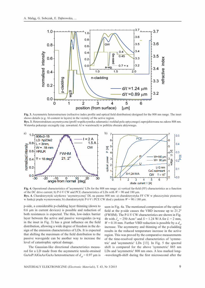
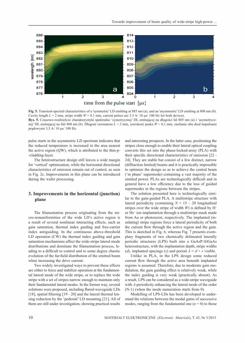
seen in Fig. 4a. The mentioned compression of the optical field at the p-side causes the VBD increase up to 21.2º (FWHM). The P-I-V CW characteristics are shown in Fig. 4b with Jth = 250 Acm-2 and S = 1.24 W/A for L = 2 mm, W = 0.18 mm. Further VBD reduction is possible by a deff increase. The asymmetry and thinning of the p-cladding results in the reduced temperature increase in the active region. This was proved by the comparative measurements of the time-resolved spectral characteristics of 'symme-tric' and 'asymmetric' LDs [13]. In Fig. 5 the spectral shift is compared for the above 'symmetric' 885 nm LDs and 'asymmetric' 808 nm ones. A less marked long--wavelength-shift during the first microsecond after the
Fig. 4. Operational characteristics of 'asymmetric' LDs for the 808 nm range: a) vertical far-field (FF) characteristics as a function of the DC drive current; b) P-I-V CW and PCE characteristics of LDs with W = 90 and 180 μm.Rys. 4. Charakterystyki użytkowe ‘asymetrycznej’ DL na pasmo 808 nm: a) charakterystyka FF CW w płaszczyźnie pionowej w funkcji prądu wysterowania; b) charakterystyki P-I-V i PCE CW diod z paskiem W = 90 i 180 μm.
a) b)
Towards improvement of beam quality of wide-stripe high-power ...
10 MATERIAŁY ELEKTRONICZNE (Electronic Materials), T. 43, Nr 3/2015
pulse starts in the asymmetric LD spectrum indicates that the reduced temperature is increased in the area nearest the active region (QW), which is attributed to the thin-p--cladding-layer.
The heterostructure design still leaves a wide margin for ‘vertical’ optimization, while the horizontal directional characteristics of emission remain out of control, as seen in Fig. 2c. Improvements in this plane can be introduced during the wafer processing.
3. Improvements in the horizontal (junction) plane
The filamentation process originating from the mi-cro-nonuniformities of the wide LD’s active region is a result of several nonlinear interacting effects, such as gain saturation, thermal index guiding and free-carrier index antiguiding. In the continuous above-threshold LD operation (CW) the thermal index guiding and gain saturation mechanisms affect the wide-stripe lateral mode distributions and dominate the filamentation process, le-ading to a difficult to control and to some degree chaotic evolution of the far-field distribution of the emitted beam when increasing the drive current.
Two widely investigated ways to prevent these effects are either to force and stabilize operation at the fundamen-tal lateral mode of the wide stripe, or to replace the wide stripe with a set of stripes narrow enough to maintain only their fundamental lateral modes. In the former way, several solutions were proposed, including flared-waveguide LDs [18], spatial filtering [19 - 20] and the lateral thermal len-sing reduction by the ‘pedestal’ LD mounting [21]. All of them are still under investigation, showing practical results
Fig. 5. Transient-spectral characteristics of a 'symmetric' LD emitting at 885 nm (a), and an 'asymmetric' LD emitting at 808 nm (b). Cavity length L = 2 mm, stripe width W = 0.1 mm, current pulses are 3.5 A/ 10 μs/ 100 Hz for both devices. Rys. 5. Czasowo-rozdzielcze charakterystyki spektralne ‘symetrycznej’ DL emitującej na długości fal 885 nm (a) i ‘asymetrycz-nej’ DL emitującej na fali 808 nm (b). Długość rezonatora L = 2 mm, szerokość paska W = 0,1 mm, zasilanie obu diod impulsami prądowymi 3,5 A/ 10 μs/ 100 Hz.
and interesting prospects. In the latter case, positioning the stripes close enough to enable their lateral optical coupling converts this set into the phase-locked-array (PLA) with their specific directional characteristics of emission [22 - 24]. They are stable but consist of a few distinct, narrow (diffraction limited) beams and it is practically impossible to optimize the design so as to achieve the central beam (‘in phase’ supermode) containing a vast majority of the emitted power. PLAs are technologically difficult and in general have a low efficiency due to the loss of guided supermodes in the regions between the stripes.
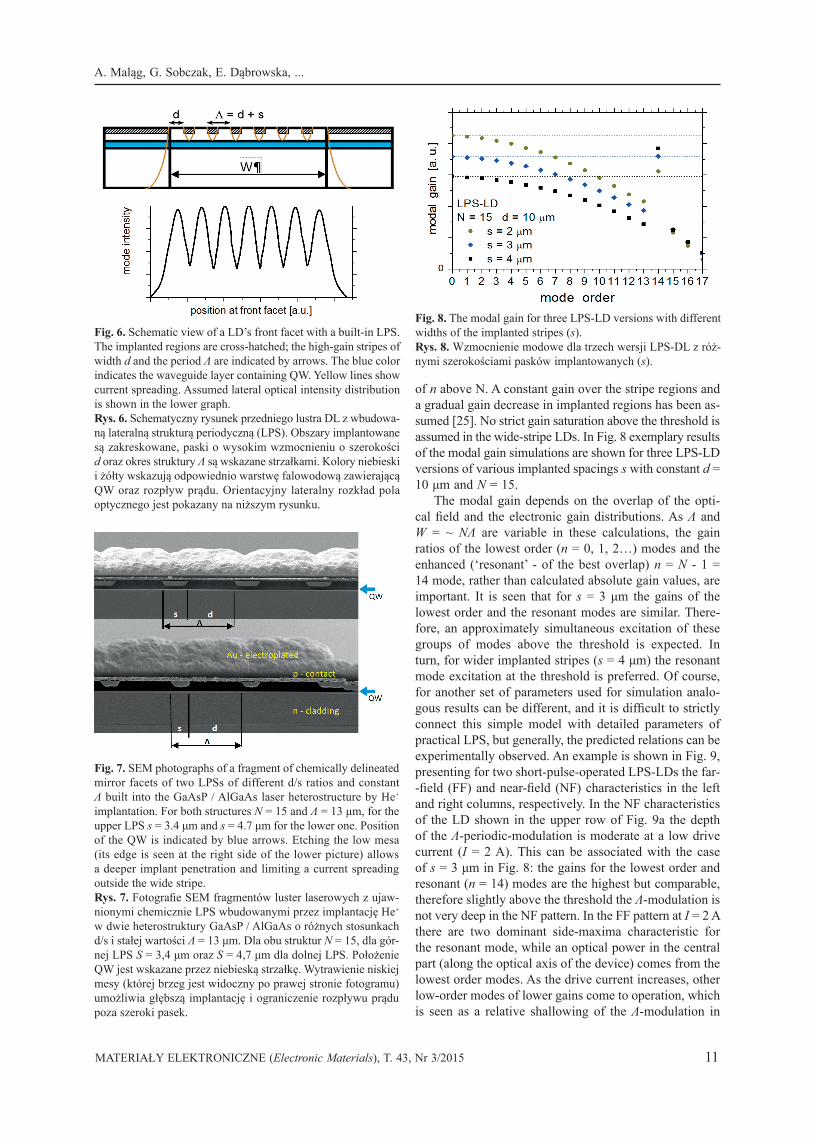
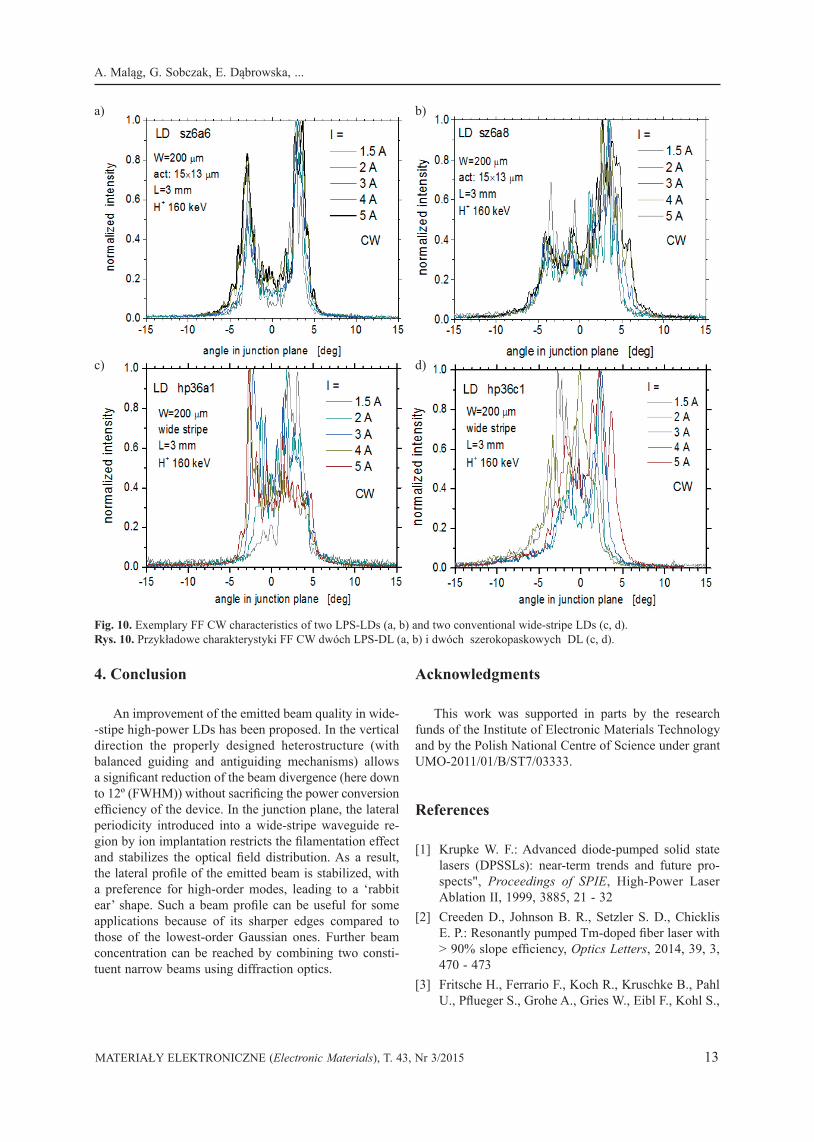
The solution presented here is technologically simi-lar to the gain-guided PLA. A multistripe structure with lateral periodicity (containing N = 15 – 20 longitudinal stripes over the wide stripe of width W) is defined by H+ or He+ ion implantation through a multistripe mask made from Au or photoresist, respectively. The implanted (in-sulating) stripe regions force a lateral periodicity of both the current flow through the active region and the gain. This is sketched in Fig. 6, whereas Fig. 7 presents exem-plary fragments of two chemically delineated laterally periodic structures (LPS) built into a GaAsP/AlGaAs heterostructure, with the implantation depth, stripe widths (d), implanted spacings (s) and period Λ = d + s visible.
Unlike in PLA, in the LPS design some reduced current flow through the active area beneath implanted regions is assumed. Therefore, due to moderate gain mo-dulation, the gain guiding effect is relatively weak, while the index guiding is very weak (practically absent). As a result, LPS can be considered as a wide-stripe waveguide with Λ-periodicity enhancing the lateral mode of the order (N-1) (when the mode numeration starts from 0).
Modelling of LPS-LDs has been developed to under-stand the relations between the modal gains of successive modes, ranging from the fundamental one (n = 0) to those
A. Maląg, G. Sobczak, E. Dąbrowska, ...
MATERIAŁY ELEKTRONICZNE (Electronic Materials), T. 43, Nr 3/2015 11
of n above N. A constant gain over the stripe regions and a gradual gain decrease in implanted regions has been as-sumed [25]. No strict gain saturation above the threshold is assumed in the wide-stripe LDs. In Fig. 8 exemplary results of the modal gain simulations are shown for three LPS-LD versions of various implanted spacings s with constant d = 10 μm and N = 15.
The modal gain depends on the overlap of the opti-cal field and the electronic gain distributions. As Λ and W = ~ NΛ are variable in these calculations, the gain ratios of the lowest order (n = 0, 1, 2…) modes and the enhanced (‘resonant’ - of the best overlap) n = N - 1 = 14 mode, rather than calculated absolute gain values, are important. It is seen that for s = 3 μm the gains of the lowest order and the resonant modes are similar. There-fore, an approximately simultaneous excitation of these groups of modes above the threshold is expected. In turn, for wider implanted stripes (s = 4 μm) the resonant mode excitation at the threshold is preferred. Of course, for another set of parameters used for simulation analo-gous results can be different, and it is difficult to strictly connect this simple model with detailed parameters of practical LPS, but generally, the predicted relations can be experimentally observed. An example is shown in Fig. 9, presenting for two short-pulse-operated LPS-LDs the far--field (FF) and near-field (NF) characteristics in the left and right columns, respectively. In the NF characteristics of the LD shown in the upper row of Fig. 9a the depth of the Λ-periodic-modulation is moderate at a low drive current (I = 2 A). This can be associated with the case of s = 3 μm in Fig. 8: the gains for the lowest order and resonant (n = 14) modes are the highest but comparable, therefore slightly above the threshold the Λ-modulation is not very deep in the NF pattern. In the FF pattern at I = 2 A there are two dominant side-maxima characteristic for the resonant mode, while an optical power in the central part (along the optical axis of the device) comes from the lowest order modes. As the drive current increases, other low-order modes of lower gains come to operation, which is seen as a relative shallowing of the Λ-modulation in
Fig. 6. Schematic view of a LD’s front facet with a built-in LPS. The implanted regions are cross-hatched; the high-gain stripes of width d and the period Λ are indicated by arrows. The blue color indicates the waveguide layer containing QW. Yellow lines show current spreading. Assumed lateral optical intensity distribution is shown in the lower graph. Rys. 6. Schematyczny rysunek przedniego lustra DL z wbudowa-ną lateralną strukturą periodyczną (LPS). Obszary implantowane są zakreskowane, paski o wysokim wzmocnieniu o szerokości d oraz okres struktury Λ są wskazane strzałkami. Kolory niebieski i żółty wskazują odpowiednio warstwę falowodową zawierającą QW oraz rozpływ prądu. Orientacyjny lateralny rozkład pola optycznego jest pokazany na niższym rysunku.
Fig. 7. SEM photographs of a fragment of chemically delineated mirror facets of two LPSs of different d/s ratios and constant Λ built into the GaAsP / AlGaAs laser heterostructure by He+ implantation. For both structures N = 15 and Λ = 13 μm, for the upper LPS s = 3.4 μm and s = 4.7 μm for the lower one. Position of the QW is indicated by blue arrows. Etching the low mesa (its edge is seen at the right side of the lower picture) allows a deeper implant penetration and limiting a current spreading outside the wide stripe.Rys. 7. Fotografie SEM fragmentów luster laserowych z ujaw-nionymi chemicznie LPS wbudowanymi przez implantację He+
w dwie heterostruktury GaAsP / AlGaAs o różnych stosunkach d/s i stałej wartości Λ = 13 μm. Dla obu struktur N = 15, dla gór-nej LPS S = 3,4 μm oraz S = 4,7 μm dla dolnej LPS. Położenie QW jest wskazane przez niebieską strzałkę. Wytrawienie niskiej mesy (której brzeg jest widoczny po prawej stronie fotogramu) umożliwia głębszą implantację i ograniczenie rozpływu prądu poza szeroki pasek.
Fig. 8. The modal gain for three LPS-LD versions with different widths of the implanted stripes (s).Rys. 8. Wzmocnienie modowe dla trzech wersji LPS-DL z róż-nymi szerokościami pasków implantowanych (s).

Towards improvement of beam quality of wide-stripe high-power ...
12 MATERIAŁY ELEKTRONICZNE (Electronic Materials), T. 43, Nr 3/2015
the NF and ‘filling’ the central part of the FF distribution. The LPS-LD represented by the lower couple of
characteristics (Fig. 9b) seems to be closer to the case of s = 4 μm in Fig. 8. Here the resonant mode is of the highest gain. As a result, the Λ-modulation of the NF distribution at I = 2 A is deeper than in the former device and maintains a relatively high depth over the measured current range up to 7 A. In the FF this is reflected as the domination of the narrow maxima of the resonant 14-th mode at ± ~ 3º over the whole current range, with a re-latively weak contribution from the lowest-order modes. The overall beam stabilization is better in this case. It must be noted, however, that a similar effect, originating from a decreasing current flow below the implanted stripes can be obtained e.g. by a deeper implantation. Generally, the FF stability is far better in LPS-LDs than in conventional wide-stripe devices.
Beam stabilization under CW operation is even more difficult due to the earlier mentioned competitive mecha-
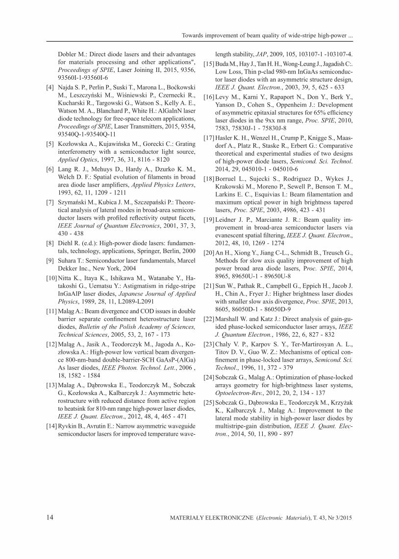
nisms of thermal index guiding and gain saturation with their lateral instabilities. It has been observed that the NF distributions that are stable as a function of a drive current in a pulsed regime become unstable under CW operation. Nonetheless, clear improvement in the CW beam stabi-lity has been recorded, which is illustrated in Fig. 10, comparing two exemplary drive-current-dependent FF characteristics of LPS-LDs (Fig. 10a, b) with the charac-teristics of two conventional wide-stripe LDs (Fig. 10c, d). Better stability of LPS-LDs is seen in terms of the beam divergence and profile (even if asymmetric).
The measured P-I-V characteristics of LPS and conven-tional LDs are similar, with Ith = 1.2 – 1.3 A (200 – 220 Acm-2) and a slope efficiency S = 0.95 – 1 W/A for asymmetric heterostructures similar to those shown above.
Further improvements are expected by Λ decreasing (restricting the movement of filaments) and optimizing the ion implantation parameters.
a)
b)
Fig. 9. Pulsed far-field normalized (left) and near-field (right) characteristics of two LPS-LDs. Vertical scales of near-field patterns are adopted to improve visibility. Rys. 9. Impulsowe charakterystyki promieniowania w strefie bliskiej i dalekiej dla dwóch LPS-DL . Skale pionowe są dobrane dla poprawy widoczności.
A. Maląg, G. Sobczak, E. Dąbrowska, ...
MATERIAŁY ELEKTRONICZNE (Electronic Materials), T. 43, Nr 3/2015 13
a) b)
c) d)
Fig. 10. Exemplary FF CW characteristics of two LPS-LDs (a, b) and two conventional wide-stripe LDs (c, d). Rys. 10. Przykładowe charakterystyki FF CW dwóch LPS-DL (a, b) i dwóch szerokopaskowych DL (c, d).
4. Conclusion
An improvement of the emitted beam quality in wide--stipe high-power LDs has been proposed. In the vertical direction the properly designed heterostructure (with balanced guiding and antiguiding mechanisms) allows a significant reduction of the beam divergence (here down to 12º (FWHM)) without sacrificing the power conversion efficiency of the device. In the junction plane, the lateral periodicity introduced into a wide-stripe waveguide re-gion by ion implantation restricts the filamentation effect and stabilizes the optical field distribution. As a result, the lateral profile of the emitted beam is stabilized, with a preference for high-order modes, leading to a ‘rabbit ear’ shape. Such a beam profile can be useful for some applications because of its sharper edges compared to those of the lowest-order Gaussian ones. Further beam concentration can be reached by combining two consti-tuent narrow beams using diffraction optics.
Acknowledgments
This work was supported in parts by the research funds of the Institute of Electronic Materials Technology and by the Polish National Centre of Science under grant UMO-2011/01/B/ST7/03333.
References
[1] Krupke W. F.: Advanced diode-pumped solid state lasers (DPSSLs): near-term trends and future pro-spects", Proceedings of SPIE, High-Power Laser Ablation II, 1999, 3885, 21 - 32
[2] Creeden D., Johnson B. R., Setzler S. D., Chicklis E. P.: Resonantly pumped Tm-doped fiber laser with > 90% slope efficiency, Optics Letters, 2014, 39, 3, 470 - 473
[3] Fritsche H., Ferrario F., Koch R., Kruschke B., Pahl U., Pflueger S., Grohe A., Gries W., Eibl F., Kohl S.,
Towards improvement of beam quality of wide-stripe high-power ...
14 MATERIAŁY ELEKTRONICZNE (Electronic Materials), T. 43, Nr 3/2015
Dobler M.: Direct diode lasers and their advantages for materials processing and other applications", Proceedings of SPIE, Laser Joining II, 2015, 9356, 93560I-1-93560I-6
[4] Najda S. P., Perlin P., Suski T., Marona L., Boćkowski M., Leszczyński M., Wiśniewski P., Czernecki R., Kucharski R., Targowski G., Watson S., Kelly A. E., Watson M. A., Blanchard P., White H.: AlGaInN laser diode technology for free-space telecom applications, Proceedings of SPIE, Laser Transmitters, 2015, 9354, 93540Q-1-93540Q-11
[5] Kozłowska A., Kujawińska M., Gorecki C.: Grating interferometry with a semiconductor light source, Applied Optics, 1997, 36, 31, 8116 - 8120
[6] Lang R. J., Mehuys D., Hardy A., Dzurko K. M., Welch D. F.: Spatial evolution of filaments in broad area diode laser amplifiers, Applied Physics Letters, 1993, 62, 11, 1209 - 1211
[7] Szymański M., Kubica J. M., Szczepański P.: Theore-tical analysis of lateral modes in broad-area semicon-ductor lasers with profiled reflectivity output facets, IEEE Journal of Quantum Electronics, 2001, 37, 3, 430 - 438
[8] Diehl R. (e.d.): High-power diode lasers: fundamen-tals, technology, applications, Springer, Berlin, 2000
[9] Suhara T.: Semiconductor laser fundamentals, Marcel Dekker Inc., New York, 2004
[10] Nitta K., Itaya K., Ishikawa M., Watanabe Y., Ha-takoshi G., Uematsu Y.: Astigmatism in ridge-stripe InGaAlP laser diodes, Japanese Journal of Applied Physics, 1989, 28, 11, L2089-L2091
[11] Maląg A.: Beam divergence and COD issues in double barrier separate confinement heterostructure laser diodes, Bulletin of the Polish Academy of Sciences, Technical Sciences, 2005, 53, 2, 167 - 173
[12] Maląg A., Jasik A., Teodorczyk M., Jagoda A., Ko-złowska A.: High-power low vertical beam divergen-ce 800-nm-band double-barrier-SCH GaAsP-(AlGa)As laser diodes, IEEE Photon. Technol. Lett., 2006 , 18, 1582 - 1584
[13] Malag A., Dąbrowska E., Teodorczyk M., Sobczak G., Kozłowska A., Kalbarczyk J.: Asymmetric hete-rostructure with reduced distance from active region to heatsink for 810-nm range high-power laser diodes, IEEE J. Quant. Electron., 2012, 48, 4, 465 - 471
[14] Ryvkin B., Avrutin E.: Narrow asymmetric waveguide semiconductor lasers for improved temperature wave-
length stability, JAP, 2009, 105, 103107-1 -103107-4. [15] Buda M., Hay J., Tan H. H., Wong-Leung J., Jagadish C:.
Low Loss, Thin p-clad 980-nm InGaAs semiconduc-tor laser diodes with an asymmetric structure design, IEEE J. Quant. Electron., 2003, 39, 5, 625 - 633
[16] Levy M., Karni Y., Rapaport N., Don Y., Berk Y., Yanson D., Cohen S., Oppenheim J.: Development of asymmetric epitaxial structures for 65% efficiency laser diodes in the 9xx nm range, Proc. SPIE, 2010, 7583, 75830J-1 - 75830J-8
[17] Hasler K. H., Wenzel H., Crump P., Knigge S., Maas-dorf A., Platz R., Staske R., Erbert G.: Comparative theoretical and experimental studies of two designs of high-power diode lasers, Semicond. Sci. Technol. 2014, 29, 045010-1 - 045010-6
[18] Borruel L., Sujecki S., Rodriguez D., Wykes J., Krakowski M., Moreno P., Sewell P., Benson T. M., Larkins E. C., Esquivias I.: Beam filamentation and maximum optical power in high brightness tapered lasers, Proc. SPIE, 2003, 4986, 423 - 431
[19] Leidner J. P., Marciante J. R.: Beam quality im-provement in broad-area semiconductor lasers via evanescent spatial filtering, IEEE J. Quant. Electron., 2012, 48, 10, 1269 - 1274
[20] An H., Xiong Y., Jiang C-L., Schmidt B., Treusch G., Methods for slow axis quality improvement of high power broad area diode lasers, Proc. SPIE, 2014, 8965, 89650U-1 - 89650U-8
[21] Sun W., Pathak R., Campbell G., Eppich H., Jacob J. H., Chin A., Fryer J.: Higher brightness laser diodes with smaller slow axis divergence, Proc. SPIE, 2013, 8605, 86050D-1 - 86050D-9
[22] Marshall W. and Katz J.: Direct analysis of gain-gu-ided phase-locked semiconductor laser arrays, IEEE J. Quantum Electron., 1986, 22, 6, 827 - 832
[23] Chaly V. P., Karpov S. Y., Ter-Martirosyan A. L., Titov D. V., Guo W. Z.: Mechanisms of optical con-finement in phase-locked laser arrays, Semicond. Sci. Technol., 1996, 11, 372 - 379
[24] Sobczak G., Maląg A.: Optimization of phase-locked arrays geometry for high-brightness laser systems, Optoelectron-Rev., 2012, 20, 2, 134 - 137
[25] Sobczak G., Dąbrowska E., Teodorczyk M., Krzyżak K., Kalbarczyk J., Maląg A.: Improvement to the lateral mode stability in high-power laser diodes by multistripe-gain distribution, IEEE J. Quant. Elec-tron., 2014, 50, 11, 890 - 897