Embed Size (px)
Citation preview

Towards Building Energy Efficient, Reliable, and Scalable NAND Flash BasedStorage Systems
The author of this item has granted worldwide open access to this work.
APA Citation: Mohan, V.(2015). Towards Building Energy Efficient, Reliable, and Scalable NANDFlash Based Storage Systems. Retrieved from http://libra.virginia.edu/catalog/libra-oa:9733
Accessed: August 15, 2016
Permanent URL: http://libra.virginia.edu/catalog/libra-oa:9733
Keywords: Architecture Power Reliability Modeling Tools Storage Systems Scalability Solid StateDisks
Terms: This article was downloaded from the University of Virginia’s Libra institutionalrepository, and is made available under the terms and conditions applicable as set forthat http://libra.virginia.edu/terms
(Article begins on next page)
Towards Building Energy Efficient, Reliable, and Scalable NANDFlash Based Storage Systems
A Dissertation
Presented to
the Faculty of the School of Engineering and Applied Science
University of Virginia
In Partial Fulfillment
of the requirements for the Degree
Doctor of Philosophy
by
Vidyabhushan Mohan
December 2015
Approvals
This dissertation is submitted in partial fulfillment of the requirements for the degree of
Doctor of Philosophy
Vidyabhushan Mohan (Author)
This dissertation has been read and approved by the Examining Committee:
Kevin Skadron (Advisor)
Jack Davidson (Chair)
Jiwei Lu
Mircea Stan
Marty Humphrey
Jack Frayer
Accepted by the School of Engineering and Applied Science:
Craig H. Benson (Dean)
December 2015
Abstract
NAND Flash (or Flash) is the most popular solid-state non-volatile memory technology used today.
As the memory technolgy scales and costs reduce, flash has replaced Hard Disk Drives (HDDs) to
become the de facto storage technology. However, flash memory scaling has adversely impacted
the energy efficiency and reliability of flash based storage systems. While smaller flash geometries
have driven storage system capacity to approach petabyte limit, performance of such high capacity
storage systems is also a major limitation. In this dissertation, we address the power, reliability, and
scalability challenges of NAND flash based storage systems by modeling key metrics, evaluating
the tradeoffs between these metrics and exploring the design space to build application optimal
storage systems.
To address the power efficiency of flash memory, this dissertation presents FlashPower, a de-
tailed analytical power model for flash memory chips. Using FlashPower, this dissertation provides
detailed insights on how various parameters affect flash energy dissipation and proposes several
architecture level optimizations to reduce memory power consumption.
To address the reliability challenges facing modern flash memory systems, this dissertation
presents FENCE, a transistor-level model to study various failure mechanisms that affect flash mem-
ories and analyze the trade-off between flash geometries and operation conditions like temperature
and usage frequency. Using FENCE, this dissertation proposes both firmware level algorithms to
enable reliable and application optimal storage systems.
Finally, to address scalability limitations of flash based high capacity Solid State Disks (SSDs),
this dissertation evaluates the bottlenecks faced by conventional SSD architectures to show that the
size of the indirection tables and the processing power available in such architectures severely limit
iii

Abstract iv
performance as SSD capacity approaches the petabyte limit. This dissertation proposes FScale, a
scalable, distributed processor based SSD architecture that can match the scaling rate of NAND
flash memory and enable high performance petabyte scale SSDs.
Legal Notice
Chapters 2, 3, and 4, Copyright © 2015 Vidyabhushan Mohan
All other chapters, Copyright © 2015 SanDisk Corp
Except for Chapters 2, 3, and 4, this dissertation and all material and know-how it contains
including my dissertation and any and all Exhibits and Annexes thereto (collectively “the Disserta-
tion”.) were developed entirely at and constitute proprietary information of SanDisk. Subject to the
University of Virginia’s right to archive and to make available my Dissertation in whole or in part
through the University’s library in all forms of media, SanDisk reserves and retains all rights, title
and interest in the Dissertation.

Acknowledgments
This dissertation would not have been possible without the help of many people and it will be
incomplete without acknowledging them.
Of all of them, I want to first thank my advisor Professor Mircea Stan. Mircea has lent a strong
hand of support and helped me navigate this journey which started in 2008. I’m grateful for freedom
that he has given me to explore ideas on my own and by allowing me to finish graduate studies even
though I was off-grounds for a significant time duration. He has always been there to listen to me
and provided valuable feedback to improve the quality of my work.
I want to thank my co-advisor, Professor Kevin Skadron. Discussions with Kevin have taught
me how to construct a problem statement, think clearly, remove the noise and find answers to the
core questions. His feedback has helped me to improve my presentation style and his insightful
comments have helped me to solidify my research ideas. I want to thank my committee mem-
bers Professor Jack Davidson, Professor Marty Humphrey and Professor Jiwei Lu for serving in
the committee and for their guidance. I also want to thank Professor Sudhanva Gurumurthi for
providing financial aid and advising me during my formative years in graduate school.
I want to thank Jack Frayer, one of the committee members and my manager at SanDisk. Jack
has been a constant source of support, encouraging me to come up with new ideas and helping me
focus on bringing those ideas to life. I want to thank Dr. Yale Ma and Nima Mokhlesi, for having
confidence and hiring me even before I completed graduate studies. I also want to thank SanDisk
for providing me the opportunity to work on cutting edge research and the support to continue my
education. I would like to thank Dr. Hongzhong Zheng and James Tringali for mentoring me and
providing the opportunity to contribute to exciting research projects as an intern.
vi

Acknowledgments vii
At UVa, I formed many new friendships that I hope will last for this lifetime. Ram’s presence
and support has helped me stay positive, seek out and cherish hard challenges and appreciate the
meaning of life. He made me feel at home, inspired me to become a long distance runner and
taught me to remain equanimous in victory and defeat. Many thanks to my roommates, Balaji,
Abhishek and Avinash for putting up with me for many years and cheering me up after a very long
day at work. I will forever cherish the late night Taco Bell dinners with Avinash and the passionate
debates with Balaji. Thanks to Chih-hao, Tanima, Enamul, Wei, Munir, Vijay, Anurag and Rukmani
for making graduate school memorable. Special thanks to Sriram for introducing me to UVa, being
a good friend and a collaborator. My sincere thanks to Taniya for being the ideal team member. Her
tenacity and work ethic inspired me and her presence made our a lab a cheerful place. Without her
and Munir, I wouldn’t have had the rare opportunity to drive cross country. I’m forever thankful to
have a friend like her.
I would like to thank my undergraduate advisor, Professor Ranjani Parthasarthi for sowing
the seeds of interest in the field of computer architecture. She encouraged me (and many of my
classmates) to explore this exciting field and to express ourselves. During tough times, I often
turned to my dear friend TS, who was always willing to provide a shoulder to lean on and let me
catch some breath.
This dissertation would not have been possible without the love, sacrifice, faith and prayers of
my parents. I cannot fathom their unwavering faith in my abilities. Amma and appa have cheered
every single success of mine, and upon each failure lifted me on to their shoulders and kept me
going. Life would be very dull without my sister who has always supported me. Between us, she
is the real doctor - someone who can find a cure for a disease and save people’s life. My wife
has been a great source of strength throughout this journey. She has remained extremely patient,
always encouraged me and managed our family as I spent many nights and weekends tucked in my
office working on completing this dissertation. Watching our son grow has been revitalizing and
keeps reminding me of the virtues of unbrindled excitement and joy in learning new things. Many
other family members have wished for my success and have gone out of their way to ensure that I
succeed. I’m forever grateful to be part of such a family.

Acknowledgments viii
Finally, thanks to the almighty for helping me complete this dissertation successfully.
Krishnarpanam asthu.

Contents
Abstract iii
Legal Notice v
Acknowledgments vi
1 Introduction 1
1.1 Major Contributions . . . . . . . . . . . . . . . . . . . . . . . . . . . . . . . . . . 3
1.1.1 Analytical Model for NAND flash Energy Dissipation . . . . . . . . . . . 3
1.1.2 Architecting Reliable Solid State Storage Devices . . . . . . . . . . . . . . 3
1.1.3 Architecture Petabyte Scale SSDs . . . . . . . . . . . . . . . . . . . . . . 4
2 Understanding NAND Flash Energy Consumption 5
2.1 Introduction . . . . . . . . . . . . . . . . . . . . . . . . . . . . . . . . . . . . . . 5
2.2 Microarchitecture of NAND Flash Memory . . . . . . . . . . . . . . . . . . . . . 6
2.2.1 Components of NAND Flash Memory . . . . . . . . . . . . . . . . . . . . 6
2.2.2 Basic Flash Operations . . . . . . . . . . . . . . . . . . . . . . . . . . . . 8
2.2.3 Architectural Layout of Flash Memory . . . . . . . . . . . . . . . . . . . 9
2.3 FlashPower: A Detailed Analytical Power Model . . . . . . . . . . . . . . . . . . 10
2.3.1 Circuit Components . . . . . . . . . . . . . . . . . . . . . . . . . . . . . 10
2.3.2 Power State Machine . . . . . . . . . . . . . . . . . . . . . . . . . . . . . 11
2.3.3 Extending FlashPower for n-bit MLC flash . . . . . . . . . . . . . . . . . 14
2.3.4 Integration with CACTI . . . . . . . . . . . . . . . . . . . . . . . . . . . 14
ix
Contents x
2.3.5 Power Modeling Methodology . . . . . . . . . . . . . . . . . . . . . . . . 15
2.3.5.1 Modeling the Parasitics of an FGT . . . . . . . . . . . . . . . . 15
2.3.5.2 Derived Parameters . . . . . . . . . . . . . . . . . . . . . . . . 17
2.3.5.3 Transition from the Powered Off to the Precharged State . . . . . 18
2.3.5.4 The Read Operation . . . . . . . . . . . . . . . . . . . . . . . . 19
2.3.5.5 The Program Operation . . . . . . . . . . . . . . . . . . . . . . 21
2.3.5.6 The Erase Operation . . . . . . . . . . . . . . . . . . . . . . . . 24
2.3.5.7 Charge pumps . . . . . . . . . . . . . . . . . . . . . . . . . . . 27
2.3.5.8 Multi-plane operation . . . . . . . . . . . . . . . . . . . . . . . 27
2.4 Experimental Setup . . . . . . . . . . . . . . . . . . . . . . . . . . . . . . . . . . 28
2.4.1 Hardware Setup . . . . . . . . . . . . . . . . . . . . . . . . . . . . . . . . 28
2.4.2 Test Procedure . . . . . . . . . . . . . . . . . . . . . . . . . . . . . . . . 28
2.5 Validation of FlashPower . . . . . . . . . . . . . . . . . . . . . . . . . . . . . . . 30
2.5.1 Validation for SLC flash . . . . . . . . . . . . . . . . . . . . . . . . . . . 32
2.5.2 Validation for 2-bit MLC flash . . . . . . . . . . . . . . . . . . . . . . . . 33
2.6 Design Space Exploration Using FlashPower . . . . . . . . . . . . . . . . . . . . 36
2.7 Related Work . . . . . . . . . . . . . . . . . . . . . . . . . . . . . . . . . . . . . 39
2.8 Summary . . . . . . . . . . . . . . . . . . . . . . . . . . . . . . . . . . . . . . . 39
3 Modeling NAND Flash Memory Reliability 41
3.1 Introduction . . . . . . . . . . . . . . . . . . . . . . . . . . . . . . . . . . . . . . 41
3.2 Overview of Flash Reliability . . . . . . . . . . . . . . . . . . . . . . . . . . . . . 42
3.2.1 Factors affecting Flash Reliability . . . . . . . . . . . . . . . . . . . . . . 42
3.2.1.1 Cycling . . . . . . . . . . . . . . . . . . . . . . . . . . . . . . 43
3.2.1.2 Recovery Period . . . . . . . . . . . . . . . . . . . . . . . . . . 43
3.2.1.3 Temperature . . . . . . . . . . . . . . . . . . . . . . . . . . . . 44
3.3 An Analytical Model for NAND Flash Data Retention . . . . . . . . . . . . . . . 45
3.3.1 Model for Data Retention . . . . . . . . . . . . . . . . . . . . . . . . . . 46
Contents xi
3.4 Impact of Detrapping on Data Retention . . . . . . . . . . . . . . . . . . . . . . . 48
3.5 Impact of Temperature on Data Retention . . . . . . . . . . . . . . . . . . . . . . 50
3.6 Related Work . . . . . . . . . . . . . . . . . . . . . . . . . . . . . . . . . . . . . 52
3.7 Summary . . . . . . . . . . . . . . . . . . . . . . . . . . . . . . . . . . . . . . . 52
4 Building High Endurance, Low Cost SSDs for Datacenters 54
4.1 Introduction . . . . . . . . . . . . . . . . . . . . . . . . . . . . . . . . . . . . . . 54
4.2 Experimental Methodology . . . . . . . . . . . . . . . . . . . . . . . . . . . . . . 57
4.2.1 SSD Configuration and Simulator Setup . . . . . . . . . . . . . . . . . . 57
4.2.2 Workloads . . . . . . . . . . . . . . . . . . . . . . . . . . . . . . . . . . 58
4.3 Simulating SSDs with HDD Workload Traces . . . . . . . . . . . . . . . . . . . . 58
4.4 Estimating SSD Lifetime Over Long Timescales . . . . . . . . . . . . . . . . . . . 60
4.5 Impact of SSD Workloads on MLC Flash Reliability . . . . . . . . . . . . . . . . 63
4.5.1 Metrics . . . . . . . . . . . . . . . . . . . . . . . . . . . . . . . . . . . . 63
4.5.2 Baseline Evaluation . . . . . . . . . . . . . . . . . . . . . . . . . . . . . 64
4.5.3 reFresh SSDs - An alternative approach to increase SSD lifetime . . . . . . 65
4.6 Related Work . . . . . . . . . . . . . . . . . . . . . . . . . . . . . . . . . . . . . 70
4.7 Summary . . . . . . . . . . . . . . . . . . . . . . . . . . . . . . . . . . . . . . . 71
5 Architecting Petabyte Scale SSDs 72
5.1 Introduction . . . . . . . . . . . . . . . . . . . . . . . . . . . . . . . . . . . . . . 72
5.2 Overview of Enterprise SSD Architecture . . . . . . . . . . . . . . . . . . . . . . 74
5.3 Modeling Conventional SSD Architectures . . . . . . . . . . . . . . . . . . . . . . 75
5.3.1 Modeling Methodology . . . . . . . . . . . . . . . . . . . . . . . . . . . 75
5.3.1.1 Hardware Model . . . . . . . . . . . . . . . . . . . . . . . . . . 76
5.3.1.2 Flash Translation Layer (FTL) Model . . . . . . . . . . . . . . . 76
5.3.1.3 Modeling FTL Latency . . . . . . . . . . . . . . . . . . . . . . 77
5.3.2 Modeling Accuracy and Relevance . . . . . . . . . . . . . . . . . . . . . 79
5.4 Scalability Challenges in Conventional SSD Architectures . . . . . . . . . . . . . 80

Contents xii
5.4.1 Metrics, Workloads . . . . . . . . . . . . . . . . . . . . . . . . . . . . . . 80
5.4.2 L2P Table Size and Cache Capacity . . . . . . . . . . . . . . . . . . . . . 81
5.4.2.1 Drawbacks in existing solutions . . . . . . . . . . . . . . . . . . 83
5.4.3 SSD Controller Utilization . . . . . . . . . . . . . . . . . . . . . . . . . . 83
5.4.4 Challenges in Scaling FTL Processor Performance . . . . . . . . . . . . . 85
5.4.5 Host Interface Processor, ECC Engine and NAND . . . . . . . . . . . . . 86
5.5 FScale: A Scalable SSD Architecture . . . . . . . . . . . . . . . . . . . . . . . . 88
5.5.1 FScale Hardware Architecture . . . . . . . . . . . . . . . . . . . . . . . . 88
5.5.1.1 FScale Hardware Architecture Assumptions . . . . . . . . . . . 89
5.5.2 FScale FTL Architecture . . . . . . . . . . . . . . . . . . . . . . . . . . . 89
5.5.2.1 Top-level FTL . . . . . . . . . . . . . . . . . . . . . . . . . . . 90
5.5.2.2 Back-end FTL . . . . . . . . . . . . . . . . . . . . . . . . . . . 90
5.6 FScale Performance Results . . . . . . . . . . . . . . . . . . . . . . . . . . . . . 91
5.6.1 L2P Table Size and Cache Capacity . . . . . . . . . . . . . . . . . . . . . 91
5.6.2 FScale Performance Analysis . . . . . . . . . . . . . . . . . . . . . . . . 93
5.6.3 Impact of Workload Queue Depth on FScale Performance . . . . . . . . . 95
5.6.4 Other Advantages of FScale Architecture . . . . . . . . . . . . . . . . . . 97
5.7 Related Work . . . . . . . . . . . . . . . . . . . . . . . . . . . . . . . . . . . . . 97
5.8 Summary . . . . . . . . . . . . . . . . . . . . . . . . . . . . . . . . . . . . . . . 98
6 Conclusions and Future Work 99
6.1 Emerging Non Volatile Memories and Evolution of Memory Hierarchy . . . . . . . 101
Bibliography 103

List of Figures
2.1 Circuit Layout of a NAND Flash Memory Plane. . . . . . . . . . . . . . . . . . . 7
2.2 Power State Machine for an SLC NAND Flash Chip . . . . . . . . . . . . . . . . . 11
2.3 Power State Machine for a 2-bit MLC NAND Flash Chip . . . . . . . . . . . . . . 12
2.4 Transition between MLC Program States. . . . . . . . . . . . . . . . . . . . . . . 13
2.5 Modeling a Floating Gate Transistor . . . . . . . . . . . . . . . . . . . . . . . . . 17
2.7 Read Energy Comparison for SLC flash . . . . . . . . . . . . . . . . . . . . . . . 31
2.8 Program Energy Comparison for SLC flash . . . . . . . . . . . . . . . . . . . . . 31
2.9 Erase Energy Comparison for SLC flash . . . . . . . . . . . . . . . . . . . . . . . 32
2.10 Read Energy Comparison for MLC flash . . . . . . . . . . . . . . . . . . . . . . . 34
2.11 Program Energy Comparison for MLC flash . . . . . . . . . . . . . . . . . . . . . 35
2.12 Erase Energy Comparison for MLC flash . . . . . . . . . . . . . . . . . . . . . . 36
3.1 Trapping and Detrapping in Floating Gate Transistors . . . . . . . . . . . . . . . . 44
3.2 Impact of Recovery Periods on SLC and MLC Flash Data Retention . . . . . . . . 49
3.3 Impact of Temperature on SLC Data Retention . . . . . . . . . . . . . . . . . . . 50
3.4 Impact of Temperature on MLC Data Retention . . . . . . . . . . . . . . . . . . . 51
4.1 Cost Analysis of SSDs in Datacenters . . . . . . . . . . . . . . . . . . . . . . . . 56
4.2 Impact of Varying Workload Intensity on SSD Response Time . . . . . . . . . . . 60
4.3 Impact of SSD Workload on M-SSD Reliability . . . . . . . . . . . . . . . . . . . 65
4.4 Impact of EDF Refresh Algorithm On the Lifetime of M-SSD . . . . . . . . . . . 68
5.1 Conventional SSD Architecture. . . . . . . . . . . . . . . . . . . . . . . . . . . . 74
xiii

List of Figures xiv
5.2 FTL Operation Types and Phases . . . . . . . . . . . . . . . . . . . . . . . . . . . 78
5.3 L2P Table Size as a function of SSD Capacity and Logical Page Size . . . . . . . . 80
5.4 Random Read Throughput as a Function of SSD Capacity . . . . . . . . . . . . . 81
5.5 SSD Controller Utilization as a Function of Drive Capacity and Workload Write
Intensity . . . . . . . . . . . . . . . . . . . . . . . . . . . . . . . . . . . . . . . . 82
5.6 Random Write Throughput as a Function of SSD Capacity . . . . . . . . . . . . . 85
5.7 FScale Hardware Architecture . . . . . . . . . . . . . . . . . . . . . . . . . . . . 87
5.8 FScale FTL Architecture . . . . . . . . . . . . . . . . . . . . . . . . . . . . . . . 87
5.9 L2P Table Size Comparison Between Conventional and FScale Architecture . . . . 92
5.10 Workload Performance with FScale Architecture . . . . . . . . . . . . . . . . . . 94
5.11 FScale Performance at Various Queue Depths . . . . . . . . . . . . . . . . . . . . 96
List of Tables
2.1 Address Map for a SLC Block. . . . . . . . . . . . . . . . . . . . . . . . . . . . . 9
2.2 Address Map for a 2-bit MLC Block. . . . . . . . . . . . . . . . . . . . . . . . . . 9
2.3 Inputs to FlashPower . . . . . . . . . . . . . . . . . . . . . . . . . . . . . . . . . 16
2.4 NAND flash chips used for evaluation . . . . . . . . . . . . . . . . . . . . . . . . 28
2.5 Different 16Gb Chip Configurations . . . . . . . . . . . . . . . . . . . . . . . . . 37
2.6 Energy dissipation for various 16Gb Chip Configurations. . . . . . . . . . . . . . . 37
2.7 Energy dissipation for various bit patterns for X1-M16. . . . . . . . . . . . . . . . 38
4.1 Properties of Enterprise Workloads Used for Evaluation. . . . . . . . . . . . . . . 58
4.2 Cross validation results for extrapolated vs measured parameters. . . . . . . . . . . 62
5.1 Major parameters for the SSD architecture model. . . . . . . . . . . . . . . . . . . 79
5.2 Comparing Cache Performance Metrics with Conventional and FScale Architecture 92
xv
Chapter 1
Introduction
We are currently in the era of data centric computing where an increasingly interconnected popu-
lation has been generating data at a pace and scale far beyond Moore's law. As the volume of data
generated increases, there is a significant need for storage devices that can not only store data per-
sistently but also retrieve them reliably, quickly and in an energy efficient manner. NAND Flash (or
Flash) based storage systems are a class of persistent storage devices that use transistors connected
together in a NAND topology to store and retrieve data. Common examples of such storage de-
vices include Universal Serial Bus (USB) drives, Secure Digital (SD) cards, and Solid State Drives
(SSDs) used in laptops, workstations and servers. Unlike other class of storage devices (like Hard
Disk Drives (HDDs) and tape), flash based storage devices do not contain any mechanical com-
ponents to store and retrieve data making them smaller, faster, robust and energy efficient. As the
physical and logical dimension of flash memory scales and the cost of memory reduces, the adop-
tion rate of flash has continued to increase. In order to facilitate this growth, system architects
are required to optimize the storage systems for specific metrics like power, reliability and perfor-
mance. While some of the optimizations can be employed at the memory chip level, others require
system level changes to enhance system metrics. The overall goal of this dissertation is to address
the power, reliability and scalability challenges of NAND flash based storage systems by modeling
the metrics, evaluating the tradeoffs between the metrics and exploring the design space to build
application optimal storage systems.
Power is an important consideration for flash memories because their design is closely tied to the
1
Chapter 1. Introduction 2
power budget of the system within which they are allowed to operate. Given that flash memories
are used in a wide range of systems, an accurate knowledge of power consumption and insights
into how power is consumed in flash are critical. There has been little research on how various
parameters affect energy dissipation as most studies rely on worst case estimates from data sheets.
The first objective of this dissertation is to dissect the internal architecture of flash memory chips and
build an analytical model of its energy dissipation. We then use the model to attain insights on flash
energy dissipation and propose architecture optimizations that can reduce the power consumption
of these memories.
NAND flash based storage systems face multiple reliability challenges. The cell-structure and
organization of transistors inside the chips coupled with high current required for reading and writ-
ing from these transistors affects their reliability significantly. As the flash transistor technology
scales down in size, the reliability issues faced by the technology are greatly exacerbated. Consider-
ing the wide disparity in the reliability requirement of various storage devices, the second objective
of this dissertation is to model important failure mechanisms that affect NAND flash based stor-
age and propose firmware and architecture level solutions that can mitigate these failures to design
application optimal storage systems.
Current storage system architectures and Error Correction Code (ECC) mechanisms have en-
abled the industry to scale storage capacity by from the gigabytes to terabytes. Over the past 10
years, the capacity of NAND based storage systems have increased by three orders of magnitude
and are expected to approach a petabyte within the next decade [22]. As memory scaling continues,
existing system architectures should also scale accordingly to manage hundreds of NAND flash
chips while providing optimal performance, reliability and energy efficiency. The third and final
objective of this dissertation is to build an architecture level model to demonstrate the challenges in
scaling current SSD architectures. In order to overcome these challenges, this dissertation proposes
a new architecture that can effectively scale with NAND capacity and provide an optimal storage
system behavior.

Chapter 1. Introduction 3
1.1 Major Contributions
The specific contributions of this dissertation are as follows.
1.1.1 Analytical Model for NAND flash Energy Dissipation
We present FlashPower, a detailed power model for the two most popular variants of NAND flash
namely, the Single-Level Cell (SLC) and 2-bit Multi-Level Cell (MLC) based NAND flash memory
chips. FlashPower models the key components of a flash chip during the read, program, and erase
operations and is highly parameterized to facilitate the exploration of a wide spectrum of flash
memory organizations. We validate FlashPower against power measurements from chips from
various manufacturers and show that FlashPower estimates are comparable to the measured values.
We present case studies to show that FlashPower can be used for designing power optimal NAND
flash memory chips for use in storage systems. This work has been published in Design Automation
and Test in Europe (DATE), 2010 and IEEE Transaction on Computer Aided Design(TCAD), 2013
[58, 59]
1.1.2 Architecting Reliable Solid State Storage Devices
We present FENCE, an analytical model to understand the factors affecting NAND flash reliability.
Using the model, we show the impact of recovery period and temperature on NAND flash data
retention. We use FENCE to explore the relationship and trade-offs between two dominant flash
failure mechanisms namely: endurance and data retention. We also use FENCE to show how
to trade-off data retention to increase endurance for NAND flash based storage devices used in
data centers. We propose firmware algorithms that exploit the trade-off to increase storage device
endurance from 6% to 56% depending on the enterprise workload while employing mechanisms to
prevent data loss. This work has been published as a tech report and presented in Flash Memory
Summit, 2012 [97].

Chapter 1. Introduction 4
1.1.3 Architecture Petabyte Scale SSDs
We study the performance of conventional enterprise SSDs by building a detailed architecture
model. Using data collected from real enterprise SSDs, we model individual hardware resources
inside the SSD controller and the interaction between the software (Flash Translation Layer) and
hardware resources. Using this model, we explore the scalability limitations of conventional enter-
prise SSDs and conclude that the size of Logical-to-Physical (L2P) address translation table and the
compute power in these SSDs severely limit their performance. Our results indicate that as SSD
capacity scales towards the petabyte limit, the performance degrades by more than 30% indicating
that existing architectures have poor scalability. To address these deficiencies, we propose FScale,
new distributed processor based SSD architecture designed to scaling enterprise SSD performance
with capacity. FScale hardware architecture comprises of many programmable and low power con-
trollers named Local Controllers that are designed to manage a NAND flash package. We evaluate
the performance of FScale architecture as a function of SSD capacity using a detailed model and
show that unlike conventional architectures, SSD performance can increase with capacity by up to
3X using the FScale architecture compared to conventional SSDs of the same capacity. We propose
a 2-level hierarchical L2P table scheme that works with FScale architecture and efficiently uses the
cache memory available in the SSDs. We show that the proposed L2P mapping scheme improves
the cache hit rate by up to 4X resulting in improved SSD performance.
The rest of this dissertation is organized as follows: In chapter 2, we present FlashPower, a
detailed analytical power model for NAND flash memories. Chapter 3 presents FENCE, a relia-
bility model for NAND flash memories. In chapter 4 we use FENCE to demonstrate the trade-offs
between different flash failure mechanisms to build high endurance Solid State Disks (SSDs) for
use in data centers. In chapter 5, we discuss the challenges in architecting petabyte scale SSDs and
propose a new architecture to overcome these challenges. Chapter 6 concludes this dissertation.

Chapter 2
Understanding NAND Flash Energy Consumption
2.1 Introduction
Quantifying the energy consumption of flash accurately is necessary for many reasons. Power is an
important consideration because the design of flash memories is closely tied to the power budget
within which they are allowed to operate. For example, flash used in consumer electronic devices
has a signicantly lower power budget compared to that of a SSD used in data centers, while the
power budget for flash used in disk based caches is between the two. In such scenarios, an accurate
knowledge of flash power consumption is beneficial. Insights into flash power consumption are also
necessary because hybrid memories use flash in conjunction with other new non-volatile memories
like Phase Change RAM and Spin-Transfer Torque RAM [45, 87]. Power aware design of such
hybrid memory systems is possible only when an accurate estimate of flash energy consumption is
available. So far, most studies that quantify the energy consumption of flash were limited to using
datasheets. But research has shown that such datasheet-derived estimates are too general and do
not take the intricacies of flash memory operations into account. Datasheets only provide average
energy estimates (which in certain cases can deviate from the actual behavior by nearly 3X) and
cannot be used when accurate estimates are required. These inaccuracies arise chiefly because
they cannot account for properties like workload behavior that have an significant impact on flash
energy consumption. In particular, we lack simulation tools that can accurately estimate the power
consumption of various flash memory configurations.
5

Chapter 2. Understanding NAND Flash Energy Consumption 6
To address this void, we present FlashPower, a detailed power model for the two most popular
variants of NAND flash namely, the Single-Level Cell (SLC) and 2-bit Multi-Level Cell (MLC)
based NAND flash memory chips. FlashPower models the key components of a flash chip during
the read, program, and erase operations, and when idle, and is highly parameterized to facilitate
the exploration of a wide spectrum of flash memory organizations. FlashPower is built on top of
CACTI [100], a widely used tool in the architecture community for studying memory organizations,
and is suitable for use in conjunction with an architecture simulator. First, we validate FlashPower
against power measurements from chips from various manufactures and we show that FlashPower
estimates are comparable to the measured values. We then illustrate the versatility of FlashPower
through a design space exploration of power optimal NAND flash memory array configurations.
The organization of the rest of this chapter is as follows. Chapter 2.2 provides an overview of
the microarchitecture and operation of NAND flash memory. Chapter 2.3 presents the details of the
power model. Chapter 2.4 explains the experimental setup while Chapter 2.5 compares the results
from FlashPower with actual chip power measurements from a variety of manufacturers. Chapter
2.6 presents a design space exploration using FlashPower. Chapter 2.7 presents the related work
and Chapter 2.8 summarizes the work.
2.2 Microarchitecture of NAND Flash Memory
In this section, we describe the components in a NAND flash memory array, how they are architec-
turally laid out and their operation.
2.2.1 Components of NAND Flash Memory
Flash is a type of EEPROM (Electrically Erasable Programmable Read-Only Memory) that supports
read, program, and erase as its basic operations. A NAND flash memory chip includes command
status registers, a control unit, a set of decoders, some analog circuitry for generating high voltages,
buffers to store and transmit data, and the memory array. An external memory controller sends
read, program or erase commands to the chip along with the relevant physical address. The main

Chapter 2. Understanding NAND Flash Energy Consumption 7
component of a NAND flash memory chip is the flash memory array. A flash memory array is
organized into banks (referred to as planes). Figure 2.1 describes a flash plane. Each plane has a
page buffer (composed of sense-amplifiers and latches) which senses and stores the data to be read
from or programmed into a plane. Each plane is physically organized as blocks and the blocks are
composed of pages. A controller addresses a flash chip in blocks and pages. Thus a plane is a
two dimensional grid composed of rows (bit-lines) and columns (word-lines). At the intersection of
each row and column is a Floating Gate Transistor (FGT) which stores a logical bit of data. In this
dissertation, the terms “cell” and “FGT” refer to the same physical entity and are used interchange-
ably. In Single-Level Cell (SLC) flash, the FGT stores a single logical bit of information, while in
Multi-Level Cell (MLC) flash, the FGT stores more than one bit of information. Even though the
term MLC flash means the number of bits stored in a FGT can be more than 1, we use the term
MLC flash mostly in the context of a 2-bit MLC flash.
Floating Gate
Transistors
(FGTs)
Block Select
Page decoder
Page Buffer
Word-
lines
(WLs)
Bit-
lines
(BLs)
String Select Transistor (SST)
Ground Select Transistor
(GST)
Pass Transistors (PTs)
Block 0
Block 1
Block 2
Block n-1
Blo
ck
D
ec
od
er
Ground Select
Line (GSL)
Source
Line (SL)
Figure 2.1: Circuit Layout of a NAND Flash Memory Plane.
A group of bits in one row of a plane constitute a page. Each NAND flash block consists of

Chapter 2. Understanding NAND Flash Energy Consumption 8
a string of FGTs connected in series with access transistors to the String Select Line (SSL), the
Source line (SL), and the Ground Select Line (GSL), as shown in Figure 2.1. The string length is
equal to the total number of FGTs connected in series. The number of pages in a block and the size
of each page are integer multiples of the string length, and the number of bit-lines running through
the block, respectively. The multiplication factor depends on the architectural layout of the block.
Section 2.2.3 explains how the blocks are laid out architecturally. A pass transistor is connected to
each word-line to select/unselect the page.
2.2.2 Basic Flash Operations
NAND flash uses Fowler-Nordheim (FN) tunneling to move charges to/from the floating gate. A
program operation involves tunneling charges to the floating gate while an erase operation involves
tunneling charges off the floating gate. Tunneling of charges to and from the FGT varies its thresh-
old voltage and bits are encoded as varying threshold voltage levels. A read operation involves
sensing the threshold voltage of the FGT. An erase is performed at the granularity of a block while
the read and program operations are performed at a page granularity. Since each FGT in a MLC
flash has more than two threshold voltage levels, a read operation for MLC flash involves multi-
ple stages to sense the correct threshold voltage level. An SLC flash has only one stage in a read
operation. Most NAND flash memories employ an iterative programming method like Incremental
Step Pulse Programming (ISPP) to program an FGT. In iterative programming, a FGT attains its
target threshold voltage through a series of small incremental steps. By controlling the duration and
the magnitude of program voltage in each step, iterative programming ensures that precise thresh-
old voltage levels are reached. After each iteration, a verify operation is performed to ensure the
required threshold voltage level is reached. If not, the operation is repeated until an upper bound
on the number of steps is reached. This upper bound is fixed during the design of the chip. If the
upper bound is reached and the target threshold voltage level is still not reached, then the program
operation fails. As the iteration count increases, the energy required for a program operation also
keeps increasing. Section 2.3.5.5 provides more details about how FlashPower estimates program
energy consumption using iterative programming. Brewer et al. provide more details on circuit and

Chapter 2. Understanding NAND Flash Energy Consumption 9
Word-line Npagesize cells Npagesize cells1 Page 0 Page 12 Page 2 Page 3.. .. .... .. ..
Npage/2 Npage −2 Npage −1
Table 2.1: Address Map for a SLC Block.
Word-line MSB of first LSB of first MSB of last LSB of lastNpagesize Npagesize Npagesize Npagesize
cells cells cells cells1 Page 0 Page 4 Page 1 Page 52 Page 2 Page 8 Page 3 Page 9.. .. .. .. .... .. .. .. ..
Npage/4 Npage −6 Npage −2 Npage −5 Npage −1
Table 2.2: Address Map for a 2-bit MLC Block.
micro-architecture of flash memory [11, 90, 92].
2.2.3 Architectural Layout of Flash Memory
While Figure 2.1 shows the circuit level layout of a flash memory plane, this section explains the
page layout in a flash memory block. We illustrate the architectural layout using a SLC and a 2-bit
MLC flash as examples, but the layout is similar for all N-bit flash. We note that the architectural
layout of SLC and MLC flash can vary even though the underlying circuit layout and implementa-
tion are identical for the two. Assuming that there are a total of Npages in a block and the size of
each page is in Npagesize, Tables 2.1 and 2.2, adapted from [102], depict the address map of a flash
memory block. In case of SLC flash, each cell stores 1-bit of information and is mapped to a logical
page. The time taken to read and program this bit is nearly the same for all pages. In case of 2-bit
MLC flash some pages are mapped to the MSB while some other pages are mapped to the LSB.
The pages corresponding to LSB are read and programmed faster compared to pages mapped to the
MSB. We will refer to pages mapped to the LSB (pages 0, 1, 2, 3, etc. in Table 2.2) as fast pages
and pages mapped to the MSB (pages 4, 5, 8, 9, etc. in Table 2.2) as slow pages.

Chapter 2. Understanding NAND Flash Energy Consumption 10
2.3 FlashPower: A Detailed Analytical Power Model
In this section, we derive a detailed analytical power model for NAND flash memory chips. Flash-
Power uses this derived model to estimate NAND flash memory chip energy dissipation during
basic flash operations like read, program and erase and when the chip is idle. Before delving into
the details of the model, we list the components that are modeled and the power state machine. We
then explain the integration of FlashPower with CACTI [100], followed by the details of the model
itself.
2.3.1 Circuit Components
With respect to Figure 2.1, the components that dissipate energy are,
• The bit-line (BL) and word-line (WL) wires.
• The SSL, GSL and SL.
• The drain, source and the gate of the SST, GST and PTs.
• The drain, source and control gate of the FGTs.
• The floating gate of the FGTs - Energy dissipated during program and erase operation.
• The Sense amplifiers (SAs) - Energy dissipated during read, program verify and erase verify
operation.
In addition to the above components, FlashPower models the energy dissipated by the block and
page decoders, and the charge pumps (that provide voltages for read, program, and erase operation).
The energy per read, program and erase operation are the sum of the energy dissipated by all the
aforementioned components. Since the energy dissipation of I/O pins varies significantly with the
design of the circuit board using the flash chip, we do not model their energy.

Chapter 2. Understanding NAND Flash Energy Consumption 11
Figure 2.2: Power State Machine for an SLC NAND Flash Chip
2.3.2 Power State Machine
Figures 2.2 and 2.3 describes the power state machine for an SLC and an MLC NAND flash chip
respectively. The circles represent the individual states, while the solid lines denote state transi-
tions. We model the energy dissipated when the chip is powered. When the chip is on, but is not
performing any operations, it is in the “precharge state”. In this state, the bit-lines are precharged
while the word-lines, and the select lines (SSL, GSL and SL) are grounded. The select lines isolate
the array electrically but the chip is ready to respond to commands from the controller.
Upon receiving a read, program, or erase command from the controller, the state machine
switches to the corresponding state. When the command is complete, the state machine switches
back to the precharge state. We model the energy dissipation of the actual operation and each state
transition. For an SLC read operation, depending on whether a page is programmed or not, the chip
is in either the “Programmed Page” or the “Unprogrammed Page” state. This can be sensed in only
one read cycle. For an SLC program operation, depending on whether the bit to be programmed is
a “0” or a “1”, the state of the chip is either in “Page 0” or “Page 1” state.
For a MLC read, the chip transitions to one of the four states, depending on whether it is

Chapter 2. Understanding NAND Flash Energy Consumption 12
Figure 2.3: Power State Machine for a 2-bit MLC NAND Flash Chip
programmed or not and whether it is a slow or a fast page. For a SLC read, there are only two states
based on whether the cell is programmed or not. FlashPower requires atleast 2 read cycles to sense
one of the four states for MLC read and two cycles to sense a SLC read.
For an MLC program operation, the state transition of the chip is a function of the bit pattern
to be programmed and whether the page is a slow page or a fast page. FlashPower models an
conventional multi-page architecture programming method as described in [91]. According to this
method, each bit cell stores two pages - a fast page and a slow page. Figure 3 lists all the states for
an MLC program while Figure 2.4 explains how the chip transitions between these states. These
transitions are based on the multi-page programming algorithm proposed in [91]. When a fast page
is programmed, the chip transitions to a “Fast Page 1” state or a “Fast Page 0” state depending on
the bit pattern. When a Slow Page is programmed, the chip transitions to one of the four slow page
states depending on the bit pattern to be programmed and the current state of the fast page. The
main difference between a transition to a “Slow Page 11” state or to a “Slow Page 01” state from
a “Fast Page 1” state is the number of steps in the iterative programming method and the threshold

Chapter 2. Understanding NAND Flash Energy Consumption 13
FastPageµ1
FastPageµ0
SlowPageµ11
SlowPageµ01
SlowPageµ00
SlowPageµ10
Figure 2.4: Transition between MLC Program States.
voltage difference between the two states. A transition to a slow page state can occur only if the
chip is already in one of the two fast page states.
While FlashPower models a canonical MLC program operation, it can also model other pro-
gramming algorithms as long as they employ iterative programming techniques similar to the multi-
page architecture model. Small changes to the MLC state machine will be needed to support such
algorithms. For example, full sequence programming is a variant of multi-page architecture algo-
rithm in which both both the slow and fast pages are programmed together. To support such an
algorithm, the state machine must transition directly from the idle state to one of the four slow page
states. Since the main difference between transitions is the number of steps in the iterative pro-
gramming method and the threshold voltage difference between the states, the programming model
does not change, but the values for individual parameters that the model takes will change.
For a MLC program operation, there is only one transition from unprogrammed to programmed
state with the unprogrammed state being digitally encoded as “1” and the program state encoded
as a “0”. For an erase operation, we consider only a single state irrespective of whether the block
is in SLC or MLC mode. Note that while we consider the bit pattern for program operation, we
do not consider the bit pattern for read or erase operation. This is because the read operation only
Chapter 2. Understanding NAND Flash Energy Consumption 14
involves sensing the threshold voltage of the cell, which is deterministic if all cells in the page
are already programmed and is non-deterministic otherwise. For an erase operation, all cells in
the block are erased irrespective of their threshold voltage state. In case of the program operation,
which involves setting the threshold voltage of the cells to one of the 2n states, the input bit pattern
makes a significant difference in the power consumption. As we show in Section 2.5, the energy
dissipated to reach a “Fast Page 0” state is significantly different from the energy dissipated to reach
a “Slow Page 00” state, which in turn is different from the energy dissipated to reach a “Slow Page
01” state. The important parameters that affect the energy dissipation for the program operation are
the threshold voltage difference and the number of verify cycles required to transition to the final
threshold voltage state from the start state, both of which are governed by the input bit pattern.
2.3.3 Extending FlashPower for n-bit MLC flash
While the state machines in Figures 2.2 and 2.3 are for SLC and 2-bit MLC flash, FlashPower
can be extended for other n-bit MLC flash variants like Three Level Cell (TLC) flash. The state
machine can be generalized for a n-bit MLC flash as follows: FlashPower has a total of 2n states
for the read operation and we can sense one of these states within n cycles. Assuming that we
employ iterative programming and multi-page architecture similar to 2-bit MLC, the model requires
a total of 2n+1 −2 states for the program operation. Since an erase operation is for an entire block
irrespective of the threshold voltage of the individual cells in the block, FlashPower has only one
state for the erase operation. For TLC flash, this corresponds to 8,14 and 1 states for read, program
and erase operation respectively. The number of steps in programming and erase method can vary
from one implementation to another and so would the difference in threshold voltage of states
between transitions. Since the program and erase model are based on these parameters, they can be
extended to support n-bit MLC flash.
2.3.4 Integration with CACTI
FlashPower is designed as a plug-in to CACTI [100], a widely used memory modeling tool. We
estimate the power consumption of array peripherals such as decoders and sense amplifiers assum-

Chapter 2. Understanding NAND Flash Energy Consumption 15
ing that they are high performance devices and for the bit-lines and word-lines assuming aggressive
interconnect projections. We also model an FGT as a CMOS transistor and then use the CMOS tran-
sistor models of CACTI to calculate the parasitic capacitance of an FGT. However, unlike CACTI,
which models individual components of SRAM and DRAM based memory systems, we have cho-
sen to model the basic operations on the flash memory. This is because, in the memories that
CACTI models, individual operations operate at the same supply voltage to drive the bit-lines and
the word-lines. For example in a SRAM-based memory, both read and write operation use the same
voltage for word-lines and bit-lines. The granularity (total bytes) of a read/write is also the same.
However for NAND flash, read, program and erase operate at different bias conditions and the
granularity of an erase differs from read/program. Since the circuitry behaves differently for these
different operations, we believe that it is more appropriate to model energy for the basic operations
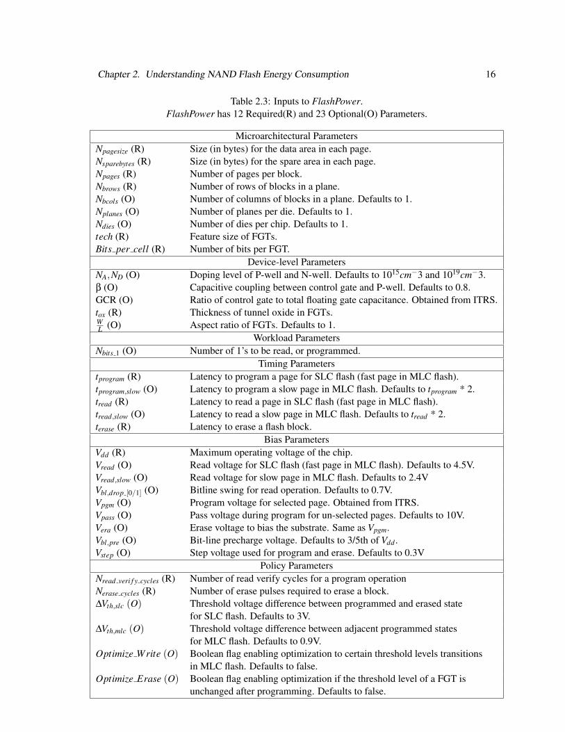
on the flash memory. Table 2.3 summarizes the inputs to FlashPower.
2.3.5 Power Modeling Methodology
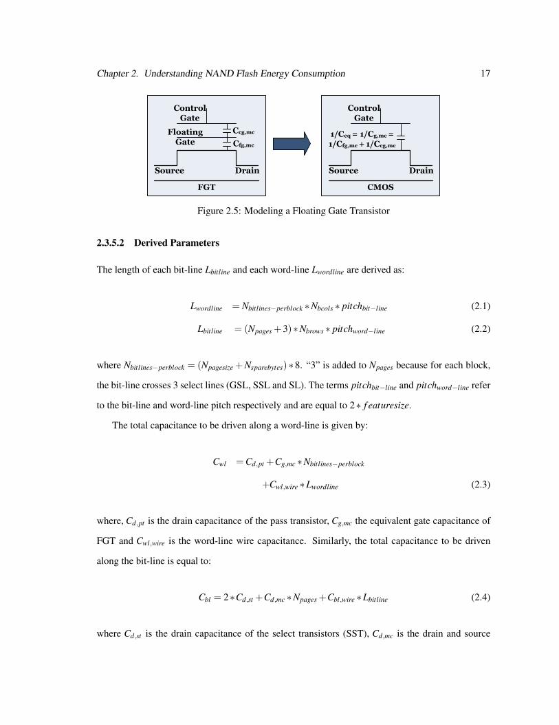
2.3.5.1 Modeling the Parasitics of an FGT
To calculate the energy dissipation of an FGT, it is necessary to estimate the FGT’s parasitic ca-
pacitance - i.e. an FGT’s source, drain and gate capacitance. While the source and the drain of
an FGT and a CMOS transistor are similar, an FGT has a two gate structure (floating and control)
while a CMOS transistor has a single gate. We model a dual gate FGT structure as an equivalent
single gate CMOS structure by calculating the equivalent capacitance of the two capacitors (one
across the inter-poly dielectric and other across the tunnel oxide). We then use CACTI to calculate
the parasitics of this transistor. Figure 2.5 illustrates this. We calculate the control gate capacitance
Ccg,mc using the information on gate coupling ratio (GCR) available in [35], while we calculate the
floating gate capacitance C f g,mc using the overlap, fringe and area capacitance of a CMOS transistor
of the same feature size. The source and drain capacitance of the transistor depend on whether the
transistor is folded or not. FlashPower assumes that the transistor is not folded as the feature size is
in the order of tens of nanometers. We use CACTI to model the drain capacitance of the FGT and
the parasitic capacitance of other CMOS transistors like the GST, PT and SST.
Chapter 2. Understanding NAND Flash Energy Consumption 16
Table 2.3: Inputs to FlashPower.FlashPower has 12 Required(R) and 23 Optional(O) Parameters.
Microarchitectural ParametersNpagesize (R) Size (in bytes) for the data area in each page.Nsparebytes (R) Size (in bytes) for the spare area in each page.Npages (R) Number of pages per block.Nbrows (R) Number of rows of blocks in a plane.Nbcols (O) Number of columns of blocks in a plane. Defaults to 1.Nplanes (O) Number of planes per die. Defaults to 1.Ndies (O) Number of dies per chip. Defaults to 1.tech (R) Feature size of FGTs.Bits per cell (R) Number of bits per FGT.
Device-level ParametersNA,ND (O) Doping level of P-well and N-well. Defaults to 1015cm−3 and 1019cm−3.β (O) Capacitive coupling between control gate and P-well. Defaults to 0.8.GCR (O) Ratio of control gate to total floating gate capacitance. Obtained from ITRS.tox (R) Thickness of tunnel oxide in FGTs.WL (O) Aspect ratio of FGTs. Defaults to 1.
Workload ParametersNbits 1 (O) Number of 1’s to be read, or programmed.
Timing Parameterstprogram (R) Latency to program a page for SLC flash (fast page in MLC flash).tprogram,slow (O) Latency to program a slow page in MLC flash. Defaults to tprogram * 2.tread (R) Latency to read a page in SLC flash (fast page in MLC flash).tread,slow (O) Latency to read a slow page in MLC flash. Defaults to tread * 2.terase (R) Latency to erase a flash block.
Bias ParametersVdd (R) Maximum operating voltage of the chip.Vread (O) Read voltage for SLC flash (fast page in MLC flash). Defaults to 4.5V.Vread,slow (O) Read voltage for slow page in MLC flash. Defaults to 2.4VVbl,drop [0/1] (O) Bitline swing for read operation. Defaults to 0.7V.Vpgm (O) Program voltage for selected page. Obtained from ITRS.Vpass (O) Pass voltage during program for un-selected pages. Defaults to 10V.Vera (O) Erase voltage to bias the substrate. Same as Vpgm.Vbl,pre (O) Bit-line precharge voltage. Defaults to 3/5th of Vdd .Vstep (O) Step voltage used for program and erase. Defaults to 0.3V
Policy ParametersNread veri f y cycles (R) Number of read verify cycles for a program operationNerase cycles (R) Number of erase pulses required to erase a block.∆Vth,slc (O) Threshold voltage difference between programmed and erased state
for SLC flash. Defaults to 3V.∆Vth,mlc (O) Threshold voltage difference between adjacent programmed states
for MLC flash. Defaults to 0.9V.Optimize Write (O) Boolean flag enabling optimization to certain threshold levels transitions
in MLC flash. Defaults to false.Optimize Erase (O) Boolean flag enabling optimization if the threshold level of a FGT is
unchanged after programming. Defaults to false.
Chapter 2. Understanding NAND Flash Energy Consumption 17
FGT
Ccg,mc
Cfg,mc
ControlGate
FloatingGate
Source Drain
CMOS
1/Ceq = 1/Cg,mc =1/Cfg,mc + 1/Ccg,mc
ControlGate
Source Drain
Figure 2.5: Modeling a Floating Gate Transistor
2.3.5.2 Derived Parameters
The length of each bit-line Lbitline and each word-line Lwordline are derived as:
Lwordline = Nbitlines−perblock ∗Nbcols ∗ pitchbit−line (2.1)
Lbitline = (Npages +3)∗Nbrows ∗ pitchword−line (2.2)
where Nbitlines−perblock = (Npagesize +Nsparebytes)∗8. “3” is added to Npages because for each block,
the bit-line crosses 3 select lines (GSL, SSL and SL). The terms pitchbit−line and pitchword−line refer
to the bit-line and word-line pitch respectively and are equal to 2∗ f eaturesize.
The total capacitance to be driven along a word-line is given by:
Cwl =Cd,pt +Cg,mc ∗Nbitlines−perblock
+Cwl,wire ∗Lwordline (2.3)
where, Cd,pt is the drain capacitance of the pass transistor, Cg,mc the equivalent gate capacitance of
FGT and Cwl,wire is the word-line wire capacitance. Similarly, the total capacitance to be driven
along the bit-line is equal to:
Cbl = 2∗Cd,st +Cd,mc ∗Npages +Cbl,wire ∗Lbitline (2.4)
where Cd,st is the drain capacitance of the select transistors (SST), Cd,mc is the drain and source

Chapter 2. Understanding NAND Flash Energy Consumption 18
capacitance of the FGT and Cbl,wire is the bit-line wire capacitance. Adjacent FGTs connected in
series share the source and the drain. Because of this assumption, the source capacitance of one
FGT is considered equal to the drain capacitance of the neighboring FGT. The source of SST is
shared with the drain of the first FGT in the string while the source of the last FGT in the string is
shared with the drain of GST. The total capacitance of the SSL is:
Cssl =Cgsl =Cd,pt +Cg,st ∗Nbitlines−perblock
+Cwl,wire ∗Lwordline (2.5)
Since the GSL needs to drive the same components as the SSL, we have Cssl =Cgsl . The capacitive
component of the SL is equal to:
Csrcline =Cwl,wire ∗Lwordline +Cd,st (2.6)
We assume that the source capacitance of GST is equal to its drain capacitance (Cd,st).
2.3.5.3 Transition from the Powered Off to the Precharged State
When this transition occurs, the bit-lines are precharged and word-lines to Vbl,pre and Vwl,pre re-
spectively. We bias the SST, GST and the PTs so that the current flowing through the FGTs is
disabled. We bias the source line to ground. Hence the energy to transition to the precharge state
(Epre) equals:
Epre = Ebl,pre +Ewl,pre (2.7)
Ebl,pre = 0.5∗Cbl,wire ∗ (0−Vbl,pre)2
∗Nbitlines−perblock ∗Lbitline (2.8)
Ewl,pre = 0.5∗Cwl,wire ∗ (0−Vwl,pre)2
∗Npages ∗Lwordline (2.9)
Chapter 2. Understanding NAND Flash Energy Consumption 19
While we precharge the bit-lines to reduce the latency of read accesses [48], the word-lines are not.
During our validation we set Vwl,pre to zero, but the model includes the word-line precharge Vwl,pre
as a parameter so that devices that perform word-line precharging can use this parameter.
2.3.5.4 The Read Operation
The read operation for SLC and MLC flash are quite similar. In case of SLC flash and fast pages
in 2-bit MLC flash, the sequence of operations required to sense the threshold voltage of the cells
is the same since we only need to distinguish between two states. In case of slow MLC pages, we
need 2 stages (and hence two read operations) to distinguish between four states.
To perform a read operation for both SLC and MLC flash, the block decoder selects one of the
blocks to be read while the page decoder selects one of the Npages inside a block. For SLC flash
and fast pages in MLC flash, we bias the word-line of the selected page to ground while we change
the bias of un-selected word-lines to Vread from Vwl,pre. This causes the un-selected pages to serve
as transfer gates. Hence the energy to bias the word-line of the selected page to ground and the
un-selected pages to Vread equals:
Eselected−page,r = 0.5∗Cwl ∗ (0−Vwl,pre)2 (2.10)
Eunselected−pages,r = 0.5∗Cwl ∗ (Vread −Vwl,pre)2
∗(Npages −1) (2.11)
For the read operation, the bit-lines remain at Vbl,pre. Depending upon the threshold voltage of the
FGT, the FGT is on or off which impacts the voltage drop in the bit-line. Assuming Nbits 1 to be
the number of bits corresponding to logical “1” and Nbits 0 to be the number of bits corresponding
to logical “0”, Vbl,drop 1 and Vbl,drop 0 to be the drop in bitline voltages for a 1-read and 0-read, the

Chapter 2. Understanding NAND Flash Energy Consumption 20
resulting energy dissipation equals:
Ebl−1,r = 0.5∗Cbl ∗ (Vbl,pre −Vbl,drop 1)2 ∗Nbits 1 (2.12)
Ebl−0,r = 0.5∗Cbl ∗ (Vbl,pre −Vbl,drop 0)2 ∗Nbits 0 (2.13)
Esl,r = Essl,r +Egsl,r +Esrcline,r (2.14)
where Vbl,drop 1 is the drop in bitline voltage when FGT is on and Vbl,drop 0 is the drop in bitline
voltage when FGT is off and Essl,r, Egsl,r and Esrcline,r are given by:
Essl,r = Egsl,r = 0.5∗Cssl ∗ (Vread −0)2 (2.15)
Esrcline,r = 0.5∗Csrcline ∗ (Vread −0)2 (2.16)
We detect the state of the cell using the sense amplifier connected to each bit-line. The sense
amplifier is a part of the page buffer and contains a latch unit [48]. It detects the voltage changes
in the bit-line and compares it with a reference voltage. Since this is very similar to DRAM sense
amplifier [99], we use CACTI’s DRAM sense amplifier model to determine the energy dissipated
for sensing and CACTI’s SRAM model to model the energy dissipated to store the sensed data in
the page buffer.
In order to read slow pages, we repeat the above steps, but instead of biasing the word-line of
the selected page to ground, we bias the word-line of the selected page to Vread,slow. If the threshold
voltage of the FGT is less than Vread,slow, then the FGT is off and the current through the bitline is
small. Otherwise, the FGT is on and the current is high. Combining the first and the second read
operation helps to distinguish between four threshold stages, thus helping to read the contents of
the slow page.
Once the read operation is complete, the system transitions from the read state to the precharged
state. This means that we bias bit-lines back to the precharge voltage Vbl,pre, while we bias the select
lines back to ground from Vread and the word-lines back to Vwl,pre. But the biasing for the transition
from read operation to precharge state is equal but opposite to the biasing for the transition from
Chapter 2. Understanding NAND Flash Energy Consumption 21
the precharge state to read operation. Hence the energy to transition from the read to the precharge
state (Er−pre) equals:
Er−pre = Ebl−1,r +Ebl−0,r +Eselected−page,r
+Eunselected−pages,r +Esl,r (2.17)
We calculate the energy dissipated by the decoders for the read operation, Edec,r, using CACTI. We
modify the CACTI decoder model to perform two levels of decoding (block and page decode) for
each read and program operation. Hence the total energy dissipated per read operation for SLC
flash and fast page of MLC flash equals:
Er = Eselected−page,r +Eunselected−pages,r +Ebl−1,r
+Ebl−0,r +Esl,r +Er−pre +Esenseamp,r +Edec,r (2.18)
The energy for a slow page read operation in MLC flash is equal to:
Er,slow = Er +Eselected−page,r +Eunselected−pages,r
+Ebl−1,r +Ebl−0,r +Esl,r +Er−pre
+Esenseamp,r +Edec,r (2.19)
where Eselected−page,r is calculated by biasing the word-line to Vread,slow instead of ground.
2.3.5.5 The Program Operation
To perform a read operation for both SLC and MLC flash, the block decoder selects one of the
blocks to be programmed while the page decoder selects one of the Npages inside a block. We trans-
fer the data from the controller to the page buffers. Since the decoding for the program operation is
the same as that of the read operation, we estimate the energy for decoding during the program op-
eration to be equal to Edec,p = Edec,r, where Edec,r is the energy for the decode operation estimated

Chapter 2. Understanding NAND Flash Energy Consumption 22
using CACTI.
FlashPower adopts the incremental step pulse programming model (ISPP) to estimate energy
dissipation during program operation [90]. In this paper, we refer to each pulse as a sub-program
operation. For each sub-program operation, we increase the program voltage of the selected page
by a step factor Vstep. After each sub-program operation, we perform a verify program operation to
check if the correct data is written to the page. If not, we repeat the sub-program operation, but with
a higher program voltage. Nread veri f y cycles indicates the total number of sub-program operations
performed during the write operation. The duration of each sub-program pulse is a function of the
program latency tprogram and Nread veri f y cycles.
We now calculate the energy for each sub-program operation. Let Vpgm,i be the program voltage
of the selected word-line in the ith iteration. We bias the selected word-line to Vpgm,i and the un-
selected word-lines to Vpass to inhibit them from programming. Since the program voltage for the
selected page varies for every iteration, we present the energy dissipated by this step as a function
of voltage. Thus the energy to bias the selected page and the un-selected page equals:
Eselected−page,p(V ) = 0.5∗Cwl ∗ (Vpgm,i −Vwl,pre)2 (2.20)
Eunselected−page,p = 0.5∗Cwl ∗ (Vpass −Vwl,pre)2
∗ (Npages −1) (2.21)
FlashPower adopts the the self-boosted program inhibit model [90] to prevent cells corresponding
to logical “1” from being programmed. According to the self-boosted program inhibit model, the
channel voltage is boosted to about 80% of the applied control gate voltage by biasing the bit-lines
corresponding to logical “1” at Vbl,ip and setting the SSL to Vdd . The resulting electric field across
the oxide is not high enough for tunneling and the cells are inhibited from being programmed.
Assuming Nbits 1 to be the number of bits corresponding to logical “1”, the energy dissipated by
Chapter 2. Understanding NAND Flash Energy Consumption 23
bit-lines to inhibit programming is equal to:
Ebl,ip = 0.5∗ (Cbl −Cd,mc ∗Npages)
∗V 2ch boost ∗Nbits 1 (2.22)
where Vch boost is the boosted channel voltage and is a fraction of applied control gate voltage.
We bias the bit-lines corresponding to logical “0” to ground. The resulting high electric field
across the tunnel oxide facilitates FN tunneling resulting in charges tunneling from the channel onto
the floating gate. The energy dissipation of bitline corresponding to logical “0” is equal to:
Ebl,p = (0.5∗ (Cbl −Cd,mc ∗Npages)∗ (0−Vbl,pre)2
+Etunnel,mc)∗Nbits 0 (2.23)
where the term Etunnel,mc is the tunneling energy per cell. Etunnel,mc is calculated as
Etunnel,mc = ∆Vth ∗ IFN ∗ tsub−program (2.24)
where IFN is the tunnel current and tsub−program is the duration of sub-program operation. IFN is
calculated as IFN = JFN ∗A f gt , where JFN is the tunnel current density calculated using [51] and
A f gt is the area of the floating gate.
Then the energy dissipated in charging the select lines is equal to:
Esl,p = Essl,p +Egsl,p +Esrcline,p (2.25)
where
Essl,p = Egsl,p = 0.5∗Cssl ∗ (Vdd −0)2
Esrcline,p = 0.5∗Csrcline ∗ (Vdd −0)2
Chapter 2. Understanding NAND Flash Energy Consumption 24
Once the sub-program operation completes, NAND flash chips perform a program-verify operation
to check if write operation is successful. FlashPower models the verify-program operation as a read
operation. Hence, the total energy per sub-program operation is:
Esubp(V ) = Eselected−page,p(V )+Eunselected−page,p
+Ebl,ip +Ebl,p +Esl,p +Evp (2.26)
where Evp, the energy spent in program verification and is given by Evp = Er −Edec,r. Er is de-
fined by equation (2.18). Since the entire process of sub-program and verify-program is repeated a
maximum of Nloop number of times, the maximum energy for programming is given by:
Epgm =Nread veri f y cycles
∑i=0
Esubp(Vpgm,i) (2.27)
Nread veri f y cycle is obtained from datasheets like [77] or can be fed as a input to the model.
Since a program operation concludes with a read operation, the transition from the Program to
Precharge is same as the transition from a read to precharge.
Ep−pre = Er−pre (2.28)
where Er−pre is given by equation (2.17).
Hence the total energy dissipated in the program operation is equal to:
Ep = Edec,p +Epgm +Ep−pre (2.29)
2.3.5.6 The Erase Operation
Since erasure happens at the block granularity, the controller sends the address of the block to be
erased. The controller uses only the block decoder and the energy for block decoding (Edec,e) is
calculated using CACTI. To aid block-level erasing, the blocks are physically laid out such that
all pages in a single block share a common P-well. Moreover, multiple blocks share the same

Chapter 2. Understanding NAND Flash Energy Consumption 25
P-well [90] and therefore it is necessary to prevent other blocks sharing the same P-well from
being erased. FlashPower assumes the self-boosted erase inhibit model [90] to inhibit other blocks
sharing the same P-well from getting erased.
Once we select an erase block, NAND flash memory uses multiple erase pulses to erase a block.
Each such operation is referred to as a sub-erase operation. The bias voltage for the P-well of the
selected block, Vera, is set to the initial program voltage, Vpgm. After each sub-erase operation, a
read-verify operation determines whether all FGTs in the block are erased or not. If all the FGTs
in the block are not erased, we repeat the erase operation (maximum of Nerase cycles times) after
incrementing Vera by the step voltage Vstep. We denote the erase voltage used for each sub-erase
operation to be Vsub−erase,i, where i indicates the iteration count of the sub-erase operation. The
duration of each sub-erase operation, tsub−erase, is a function of the maximum erase latency and
Nerase cycles.
For each sub-erase operation, we bias the control gates of all the word-lines in the selected
block to ground. We bias the P-well for the selected block to erase voltage Vsub−erase,i and the SSL
and the GSL to Vsub−erase,i ∗ β, where β is the capacitive coupling ratio of cells between control
gate and the P-well. A typical value of β is 0.8 [11]. We bias the SL to Vbl,e. Here Vbl,e is equal
to Vsub−erase,i −Vbi where Vbi is the built-in potential between the bitline and the P-well of the cell
array [76]. Adding up the charging of the SSL, GSL and SL, we get the energy dissipated in the
select lines to be:
Esl,e = Essl,e +Egsl,e +Esrcline,e (2.30)
where Essl,e,Egsl,e and Esrcline,e are calculated using the SSL, GSL and SL capacitance and the
bias condition explained above. We bias the bit-lines to Vbl,e which dissipates energy that is modeled
as:
Ebl,e(V ) = 0.5∗Cbl ∗ (Vbl,e −Vbl,pre)2 ∗Nbitlines−perblock (2.31)
We parameterize Ebl,e(V ) as a function of applied erase voltage, since the erase voltage changes for
each sub-erase operation.
With the P-well biased to Vsub−erase,i, cells that have high threshold voltage undergo FN tunnel-

Chapter 2. Understanding NAND Flash Energy Consumption 26
ing. Electrons tunnel off the floating gate onto the substrate and the threshold voltage of the cell is
reduced. To effect FN tunneling, the depletion layer capacitance between the P-well and the N-well
should be charged. This capacitance of the junction between the P-well and the N-well, which form
a P-N junction, is a function of the applied voltage Vera, the area of the p-well Awell . The dynamic
power to charge this capacitance as the voltage across the junction raises from 0V to Vsub−erase,i is
determined as:
E junction,e(V ) = (C j0
(1−Vsub−erase,i/φ0)m ∗A f gt)∗V 2sub−erase,i (2.32)
where C j0 is the capacitance at zero-bias condition and φ0 is the built-in potential of the P-N junc-
tion. m, the grading coefficient is assumed to be 0.5. We parameterize E junction,e as a function of
applied erase voltage since the erase voltage changes for each sub-erase operation.
Once this P-N junction capacitance is fully charged, all cells in the block are erased. The
tunneling energy for the block, Etunnelerase,mc, is calculated using equation (2.24) and a sub-erase
pulse whose duration is tsub−erase. After each sub-erase pulse, a verify erase operation is performed
to ensure that all FGTs in the block are erased [90]. The verify erase operation is a single read
operation which consumes energy equivalent to a read operation. This is modeled as, Eblock,ve =
Er −Edec,r where Er is given by equation (2.18).
Since the erase voltage changes for each sub-erase operation, the total energy consumed in each
sub-erase operation, Esub−erase is parameterized as a function of the voltage and is equal to:
Esub−erase(V ) = Esl,e +Ebl,e(V )+Etunnelerase,mc(V )
+E junction,e(V )+Eblock,ve (2.33)
Since an erase operation ends with a read operation, the transition from the erase to precharge is
same as the transition from read to precharge. The energy dissipated during this transition is equal
to:
Ee−pre = Er−pre (2.34)

Chapter 2. Understanding NAND Flash Energy Consumption 27
where Er−pre is given by equation (2.17).
Hence the total energy dissipated in erase operation Eerase is equal to:
Eerase = Edec,e +Nerase cycles
∑i=0
Esub−erase(Vsub−erase,i)
+Ee−pre (2.35)
We can observe that if all the cells in the block are programmed and are at a low threshold
voltage stage, then an erase operation is not necessary. Some controllers can identify this scenario
and prevent an erase operation even when they receive such a command, thereby reducing the power
consumption and the latency of the erase operation.
2.3.5.7 Charge pumps
Each read, sub-program, or sub-erase operation requires that the charge pump supply a high voltage
(5V-20V) to the flash memory array. Ishida et. al specify that the energy consumed for each high
voltage pulse from the charge-pumps is 0.25µJ for chips operating at 1.8V and 0.15µJ for chips
operating at 3.3V for the read and program operation [33]. In FlashPower, we use these constant
values but since FlashPower is parameterized, a detailed charge-pump model can be incorporated
in lieu of the current one.
2.3.5.8 Multi-plane operation
The power model described thus far corresponds to single-plane operations. However modern
NAND flash chips allow multiple planes to operate in parallel. These are referred to as multi-plane
operations. Since FlashPower models single-plane operations, energy consumption for multi-plane
operations can be determined by multiplying the results of single-plane operations with the number
of planes operating in parallel.
So far, we have provided an detailed analytical model that estimates the energy dissipation of
NAND flash for individual operations. We now validate our model with measurements from real
flash chips from various manufacturers.

Chapter 2. Understanding NAND Flash Energy Consumption 28
Chip Feature Page Size Spare Pages Blocks Planes Dies CapacityName Size (nm) (KB) (bytes) /Block /Plane /Die /Chip (Gb)
B-MLC8 72 2KB 64 128 2048 2 1 8.25D-MLC32 80 4KB 128 128 2096 2 2 33.77E-MLC64 51 4KB 128 128 2048 4 2 66.00A-SLC4 73 2KB 64 64 2048 2 1 4.13B-SLC4 72 2KB 64 64 2048 2 1 4.13
Table 2.4: NAND flash chips used for evaluation
2.4 Experimental Setup
To validate the model’s usability and accuracy, we measured the latency and energy consumption of
read, program, and erase operations from real flash chips. Using a custom-built board, we acquired
fine-grain measurements of a diverse set of flash chips. In this section, we describe the hardware
setup and the test procedure.
2.4.1 Hardware Setup
Figure 2.6 depicts our flash characterization board that consists of two sockets for testing flash chips.
The board connects to a Xilinx XUP development kit with a Virtex-II FPGA and an embedded
PowerPC processor. The processor runs Linux and connects to a custom flash controller that gives
the user complete access to the flash chips. The flash controller can issue operations to the chips
and record latency measurements with a 10 ns resolution.
To measure the energy consumption of individual flash operations, we use a high-bandwidth
current probe attached to a mixed-signal oscilloscope. The Agilent 1147A current probe attaches to
a jumper that provides power to a single flash chip. We trigger the oscilloscope to capture current
measurements when the flash controller sends a command to the flash chip.
2.4.2 Test Procedure
Table 2.4 summarizes the system-level properties of the flash chips we used for validation. We
selected a diverse set of chips - in terms of feature size, capacity, array structure, and manufacturer
- to depict the compatibility and adaptability of FlashPower.

Chapter 2. Understanding NAND Flash Energy Consumption 29
Figure 2.6: Flash Evaluation Board
We measured the latency and power consumption for read, program, and erase operations on
each chip. The types of operations we performed varied for SLC- and MLC-based flash chips.
SLC chips We tested four states for a single-page read operation on SLC-based chips: unpro-
grammed (freshly-erased), all 0’s, 50% 0’s, and all 1’s. For the program operation, we acquired data
while programming a single page with all 0’s, 50% 0’s, and all 1’s. Finally, for erase operations,
we measured the energy while erasing an entire block of pages programmed with all 0’s and pages
programmed with all 1’s.
MLC chips To quantify energy consumption for read operations of MLC-based chips, we mea-
sured the energy consumption of reading a page in four states:
1. Fast Page Programmed - Reading a programmed fast page.
2. Slow Page Programmed - Reading a programmed slow page.
3. Fast Page Unprogrammed - Reading a freshly-erased fast page.
4. Slow Page Unprogrammed - Reading a freshly-erased slow page.
For program operations, we measured the energy consumption of the following six transitions
caused by programming a page:

Chapter 2. Understanding NAND Flash Energy Consumption 30
1. Fast Page 0 - Programming a freshly-erased fast page with all 0’s.
2. Fast Page 1 - Programming a freshly-erased fast page with all 1’s.
3. Slow Page 01 - Programming a slow page with all 1’s and the fast page counterpart is of type
Fast Page 0.
4. Slow Page 11 - Programming a slow page with all 1’s and the fast page counterpart is of type
Fast Page 1.
5. Slow Page 00 - Programming a slow page with all 0’s and the fast page counterpart is of type
Fast Page 0.
6. Slow Page 10 - Programming a slow page with all 0’s and the fast page counterpart is of type
Fast Page 1.
For erase operations, we measured the energy consumption of erasing an entire block of fully-
programmed pages of all 0’s and all 1’s.
For each chip and each type of operation, we performed ten measurements and reported the
average. We summarize the results of these experiments in conjunction with the model’s approxi-
mations in Section 2.5.
2.5 Validation of FlashPower
We now compare the outputs of the analytical model with power measurements from real SLC
and MLC flash chips. The sources used to obtain values for parameters used in our model (listed
in Table 2.3) are as follows: Except for feature size of FGTs, values for all microarchitectural
parameters are obtained from manufacturer datasheets. The feature size of FGTs used in our chips
are obtained from [23, 83]. Values for device-level parameters are obtained from [11, 35, 76]. The
operating voltage of the chip is obtained from datasheets, while for other bias parameters we use
information available in Chapter 6 of [11]. The value for timing parameters and policy parameters
are deduced from datasheets, by measuring the latency of flash operations, and from [11]. We used

Chapter 2. Understanding NAND Flash Energy Consumption 31
Figure 2.7: Read Energy Comparison for SLC flash
Figure 2.8: Program Energy Comparison for SLC flash
the measured latencies of each flash operation (see Section 4.2) because we found that the values
for timing parameters and program verify cycles in datasheets were significantly different (as high
as 50% in some cases) from actual behavior. While datasheets contained average latencies of flash
operation, the actual latencies depended on factors like the type of page and in some cases on the
data pattern being used. Finally, since we measure the energy consumption of the chips by varying
the input bit pattern, we control the values for the workload parameters.
We now present the results for read, program and erase operation for both MLC flash followed
by SLC flash.

Chapter 2. Understanding NAND Flash Energy Consumption 32
Figure 2.9: Erase Energy Comparison for SLC flash
2.5.1 Validation for SLC flash
Figures 2.7, 2.8 and 2.9 show the results for the read, program and erase operations for SLC flash.
The y-axis represents the energy consumption of the particular operation, while the x-axis repre-
sents the state of a page in SLC flash as explained in Section 2.3.2. From Figure 2.7, we can observe
that the variation between the estimated and the measured read energy is about 40% on average (at
most 62% or 8µJ) for A-SLC4, while it is less than 10% for B-SLC4. For the program operation,
the difference between estimates and measurements is 22% on average (at most 26% or 2µJ) for
B-SLC4, while the difference is 40% on average (at most 62% or 8µJ) for A-SLC4. For the erase
operation, it is 24% on average ( at most 27% or 8µJ) for B-SLC4, while it is 36% on average (at
most 37% or 24µJ) for A-SLC4.
These results show that the FlashPower can estimate the energy consumption of B-SLC4 with
high accuracy, but for A-SLC4, the accuracy is low. It should be noted that the differences among
the the measured values of the two chips is similar. In other words, the estimates of A-SLC4 and B-
SLC4 are comparable among themselves, while the differences in measurements between A-SLC4
and B-SLC4 are high.
To understand why such variations occur, we compare the parameters of the two chips. We find
that the microarchitectural parameters for the two chips are almost the same (please refer to Table
2.4). Since the feature size and the operating voltage of the two chips are almost the same, our
model assumes that the device level parameters are same. As far as the timing parameters are con-

Chapter 2. Understanding NAND Flash Energy Consumption 33
cerned, our experiments show that the read latency of A-SLC4 is about 20% higher than B-SLC4.
The program latency for the two chips is similar, while the erase latency is about 30% higher for A-
SLC4 compared to B-SLC4. With respect to the policy parameters mentioned in Table 2.4, values
for ∆Vth,slc is set based on [35] and since the chips have the almost same feature size, their values
are same. The values of program-verify and erase cycles are set using latency measurements from
the chips and they are similar. Since the bit patterns are constant across both the chips, we hypothe-
size that the differences in energy are due to changes to specific policy parameters like ∆Vth,mlc and
Nread veri f y cycles, device parameters like β and tox or due to manufacturer-specific optimizations of
the individual operations. Better knowledge about the values for these parameters can significantly
increase the accuracy of the model. FlashPower is developed based on [11, 48, 90, 92] and de-
scribes the canonical operation of NAND flash memory and does not capture manufacturer-specific
designs. This results in a significant variation between estimates and measurements for A-SLC4
while the variation is significantly lower for B-SLC4. However, since FlashPower is extensively
parameterized, any manufacturer-specific implementations can be used for estimating flash power
consumption.
2.5.2 Validation for 2-bit MLC flash
Figure 2.10 shows the results for the read operation for MLC flash. The x-axis represents the page
being read during the operation while the y-axis represents the total energy dissipated during the
read. Each column represents the average energy consumed by the flash chip when it is at one of
the various states described in Section 2.3.2. From the figure, we can observe that the difference
between estimated and measured energy is less than 22.3% (or 0.64µJ) for all types of pages.
We found that the difference in estimated and measured energy values were significantly higher
for unprogrammed pages than for programmed pages. Since the threshold voltage states of cells in
unprogrammed pages is non-deterministic, modeling the energy consumption for an unprogrammed
page is challenging. It should be noted that reading an unprogrammed page does not happen often
in practice. If we just consider programmed pages, the difference drops to less than 12.3% (or
0.35µJ) and in most cases, the difference between measured and estimated values are negligible.
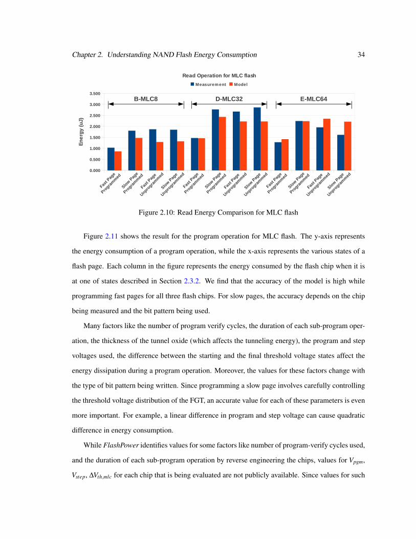
Chapter 2. Understanding NAND Flash Energy Consumption 34
Figure 2.10: Read Energy Comparison for MLC flash
Figure 2.11 shows the result for the program operation for MLC flash. The y-axis represents
the energy consumption of a program operation, while the x-axis represents the various states of a
flash page. Each column in the figure represents the energy consumed by the flash chip when it is
at one of states described in Section 2.3.2. We find that the accuracy of the model is high while
programming fast pages for all three flash chips. For slow pages, the accuracy depends on the chip
being measured and the bit pattern being used.
Many factors like the number of program verify cycles, the duration of each sub-program oper-
ation, the thickness of the tunnel oxide (which affects the tunneling energy), the program and step
voltages used, the difference between the starting and the final threshold voltage states affect the
energy dissipation during a program operation. Moreover, the values for these factors change with
the type of bit pattern being written. Since programming a slow page involves carefully controlling
the threshold voltage distribution of the FGT, an accurate value for each of these parameters is even
more important. For example, a linear difference in program and step voltage can cause quadratic
difference in energy consumption.
While FlashPower identifies values for some factors like number of program-verify cycles used,
and the duration of each sub-program operation by reverse engineering the chips, values for Vpgm,
Vstep, ∆Vth,mlc for each chip that is being evaluated are not publicly available. Since values for such

Chapter 2. Understanding NAND Flash Energy Consumption 35
Figure 2.11: Program Energy Comparison for MLC flash
parameters are not publicly available, the variation between estimates and measurements are high
for some bit patterns. For example, in the case of B-MLC8, increasing Vpgm and ∆Vth,mlc reduced
the difference between the measurement and the estimates for the Slow Page 00 and Slow Page 11
states from 49% to nearly 8%. In the case of D-MLC32, even a small decrease in Vpgm and ∆Vth,mlc
reduces the variation between estimates and measurement for the Slow Page 11 state 49% to nearly
10%. Since FlashPower has been extensively parameterized, any user who has detailed information
on individual parameters can feed those parameters into FlashPower to get an accurate estimate of
flash energy consumption.
Figure 2.12 shows the results for the erase operation for the three chips for 2 different bit
patterns. For B-MLC8 and D-MLC32, changing the bit pattern did not affect the erase energy
significantly. For E-MLC64, when all pages in the block were in the lowest threshold state (“11”),
the erase energy was about 5X lower than the energy consumption for all other bit patterns. We call
this the optimize erase operation, where the controller does not erase a block where all cells already
have the lowest threshold voltage. While two chips, B-MLC8 and D-MLC32, did not perform this
optimization, E-MLC64 had this optimization enabled. From this figure, we can also see that the
estimates correspond well to the measurements. The variation between estimates and measurement
in less than 10% for B-MLC8 and E-MLC64, while the difference was less than 20% for D-MLC32.
So far, we have examined the accuracy of FlashPower by comparing the results with measure-

Chapter 2. Understanding NAND Flash Energy Consumption 36
Figure 2.12: Erase Energy Comparison for MLC flash
ments from a range of chips across various manufacturers. We now use the tool to perform some
design space exploration studies.
2.6 Design Space Exploration Using FlashPower
FlashPower enables us to study the effect of various flash parameters (listed in Table 2.3) on the
power consumption of the chip. In this section, we show the utility of FlashPower through two case
studies to identify power optimal design configurations.
Case Study 1: Let us say a chip architect decides to design a 16Gb NAND flash chip and
wants to estimate the energy consumption for various design scenarios. Table 2.3 provides a list of
all parameters that can be adjusted by the architect to identify the relative benefits of each design
scenario. Assuming that the designer has the flexibility to change the memory array configuration
of flash, we show how to use FlashPower to compare some configurations. For this study, we vary
the microarchitecture parameters listed in Table 2.3, except the feature size, while the values for
all other parameters are assumed to be the same as the B-MLC8 chip. Table 2.5 provides a list of
configurations for designing a 16Gb memory chip.
Table 2.6 shows the read, write and erase energy for different memory configurations while
reading and programming a fast page and erasing a block. Note that, in the case of X3-M16, read

Chapter 2. Understanding NAND Flash Energy Consumption 37
Chip Page Spare Pages/ Blocks/ Planes/ Dies/Name Size (KB) Bytes Block Plane Die Chip
X1-M16 2 64 128 2048 2 2X2-M16 2 64 128 4096 2 1X3-M16 4 128 128 2048 2 1X4-M16 2 64 256 2048 2 1X5-M16 2 64 128 2048 4 1
Table 2.5: Different 16Gb Chip Configurations
ConfigurationRead Energy Program Energy Erase Energy
Fast Page Fast Page (µJ)Programmed (µJ) (µJ)
X1-MLC16 1.085 15.418 117.602X2-MLC16 1.629 18.297 232.577X3-MLC16 1.632 29.747 232.908X4-MLC16 1.59 18.205 227.719X5-MLC16 1.277 15.562 117.595
Table 2.6: Energy dissipation for various 16Gb Chip Configurations.
and program operations occur at 4KB granularity, while for other configurations, they occur at a
2KB granularity. The block size is 512KB for X3-M16 and X4-M16, while it is 256KB for the other
configurations. Table 2.6 can be used by the architect to estimate the energy dissipation for various
memory configurations. From Table 2.6 we can see that X1-M16 is the chip that dissipates the
least energy for read and program operations (for erase operation, the energy dissipation is almost
the same as X5-M16). However, the page size of X1-M16 is just 2KB. The page size for X3-
M16 is 4KB, while the energy consumption of reads is only 60% more than X1-M16. Depending
upon whether the architect is optimizing for total energy consumption or energy dissipated per byte
processed, they can choose one design over the other. In systems that run on battery power and
have small data access granularity like consumer electronics devices and wireless sensors , where
the architect is limited by maximum energy dissipation of the chip, X1-M16 is better option that X3-
M16. In systems where energy efficiency is of higher importance than maximum energy dissipation,
X3-M16 is a better option. Some designers may choose X5-M16 over the rest because the number
of planes in X5-M16 is higher than the rest, which allows for more operations to happen in parallel.
Note that for X3-M16, the write and erase energy, is still ∼2X higher than X1-M16, because their

Chapter 2. Understanding NAND Flash Energy Consumption 38
ConfigurationRead Energy Program Energy Erase Energy
Fast Page Fast Page (µJ)Programmed (µJ) (µJ)
All 1s 1.182 8.385 2.566/115.21875% 1s 1.023 10.144 115.22150% 1s 0.863 11.902 115.22425% 1s 0.703 13.660 115.226All 0s 0.543 15.418 115.229
Table 2.7: Energy dissipation for various bit patterns for X1-M16.
pages are larger.
Case Study 2: Let us say a chip architect decides to design a NAND flash chip that can consume
less energy while storing specific data patterns. This scenario could be motivated by an application
behavior or due to flash aware encoding schemes that seek to increase flash lifetime by favoring one
bit pattern over an another. For example, a flash aware encoding scheme can choose to write more
logical 1s than logical 0s in order to reduce the probability of tunneling of cells, thereby increasing
flash lifetime. FlashPower allows the architect to estimate the impact of energy dissipation due to
different bit patterns. Table 2.7 shows the energy dissipation of X1-M16 for read, write and erase
operations for various bit patterns. These results are based on the assumption that there is 100%
bitline discharge for logical 1s and no discharge for logical 0s during the read operation. From Table
2.7, we can see that for a read operation, a page filled with 0s consume less energy than a page with
1s because bit-lines corresponding to logical 0 do not discharge while bit-lines corresponding to
logical 1 discharges fully and hence dissipates more energy. However, in case of write operations,
writing logical 1s consumes less energy because programming is inhibited for logical 1s, while
tunneling happens when logical 0s are written, consuming more energy. For erase operations, if the
chip supports optimize erase feature, then the erase energy is just 2.5µJ. Without optimization, this
increases by 46X to 115.128µJ, indicating the importance of optimizating erase operations. The
erase energy does not vary significantly with the data pattern since the entire P-well of the erase
block is biased to the erase voltage Vera and hence dissipate almost the same energy.
These two case studies show the utility of FlashPower in evaluating the design tradeoffs for
NAND flash memory. Because FlashPower is parameterized, it is possible to analyze such what-if
Chapter 2. Understanding NAND Flash Energy Consumption 39
scenarios and identify power optimal flash chip configurations.
2.7 Related Work
CACTI is an integrated timing, area, leakage and power modeling tool from HP Labs [100]. CACTI
supports evaluating SRAM and DRAM memory technologies. This chapter uses the underlying in-
frastructure available in CACTI and extends it to model NAND flash memories. Research interest in
non-volatile memories has spawned development of analytical models for many memory technolo-
gies, most of which use CACTI as their base. Smullen et al. provide an analytical model to charac-
terize the behavior of Spin-Transfer Torque RAM (STT-RAM) [86]. Dong et al. provide a similar
analytical model for phase change memories [18]. Xu et al. extend CACTI to model Resistive RAM
(RRAM) memory technology [101]. While analytical models form one end of the spectrum, charac-
terizing memory technologies with actual measurements form the other end. Grupp et al. provide a
characterization of physical properties using actual measurements from flash chips [23]. Yaakobi et
al. use results from actual measurements to characterize the reliability of flash chips [102]. Boboila
et al. perform a similar study, but focus mainly on write endurance [10]. NVSim presents ana-
lytical models for flash with validations at a datasheet level [64]. FlashPower uses measurements
from actual chips and combines it with a detailed parameterized analytical model for NAND flash
memories. NANDFlashSim is a microarchitecture level tool that simulates only the performance
characteristics of NAND flash chips [42]. NANDFlashSim can be used on top of circuit-level ana-
lytical modeling tools like FlashPower to provide a flash simulation infrastructure that models both
energy and performance.
2.8 Summary
In this chapter, we have presented FlashPower, a detailed power model for the two most popular
variants of NAND flash namely, the Single-Level Cell (SLC) and 2-bit Multi-Level Cell (MLC)
based NAND flash memory chips. FlashPower models the energy dissipation of flash chips from
first principles and is highly parameterized to study a large design space of memory organizations.

Chapter 2. Understanding NAND Flash Energy Consumption 40
We have validated FlashPower against measurements from 5 different chips from different man-
ufacturers and show that our model can accurately estimate the energy dissipation of several real
chips.

Chapter 3
Modeling NAND Flash Memory Reliability
3.1 Introduction
NAND Flash memory is used in a wide range of systems ranging from consumer electronics de-
vices like Secure Digital (SD) cards and smart phone storage to Solid State Disks (SSDs) in data
centers. Due to this wide application, NAND flash based storage systems have diverse reliability
requirements. A storage device like a SD card may require data to be stored for several years but
may be written only a few hundred times. However, a SSD used in data center may be written
several thousand times while the data is expected to remain non-volatile only for a few weeks or
months due to the periodic backup operations. In order to understand the reliabilty of NAND based
storage systems, a comprehensive understanding of the physical behavior of the memory and vari-
ous reliability mechanisms along with system parameters (like workload and ambient temperature)
used to exercise the storage device is required. In this chapter, we study the major failure mecha-
nisms associated with NAND flash using a detailed analytical model. We then use the analytical
model to quantify failure at the memory level and study sensitivity to important parameters like
temperature and recovery periods. We then use the model to study the trade-offs among the failure
mechanisms at the memory level. In Chapter 4, we use the memory level reliability understanding
obtained using these models to study the system level reliability of SSDs used in data centers.
The rest of this chapter is organized as follows: Section 3.2 provides an overview of NAND
flash reliability. Section 3.3 describes an analytical model for NAND flash data retention, while
41
Chapter 3. Modeling NAND Flash Memory Reliability 42
Section 3.4 analyzes the impact of detrapping on data retention. In Section 3.5, we study the effect
of temperature on data retention while we discuss related work in Section 3.6. We summarize this
chapter in Section 3.7.
3.2 Overview of Flash Reliability
The main types of reliability issues in NAND flash memory are: data retention, write endurance,
and disturbs. The duration of time for which the data written in flash memory cells can be read
reliably is called the (data) retention period. The number of Program/Erase (P/E) cycles that can
be performed on flash cells while guaranteeing a particular retention period determines the (write)
endurance. While the retention period and endurance of flash can vary with usage, flash manu-
facturers guarantee a retention period in the order of years and an endurance of 3000 to 100,000
P/E cycles [34, 72]. Loss of data retention and write endurance are the most dominant flash re-
liability Memory cell disturbs occur when a bit flips inadvertently in that cell due to accesses to
adjacent cells. There can be read, write, or erase disturbs, depending on the operation in the ad-
jacent cells. Many studies have shown that NAND flash memory has very low vulnerability to
disturbs and that erasing the cell (which occurs several times as part of the normal usage of the
SSD, since NAND flash does not support in-place writes) reduces the susceptibility of memory
cells to bit flips [14, 93]. Moreover, existing Error Correction Codes (ECC) in flash memory are
effective in handling errors that occur due to disturbs [14]. Therefore this paper focuses only on
endurance and retention time and the tradeoffs between the two. Memory standards organizations,
such as Joint Electron Device Engineering Council (JEDEC), provide detailed information about
these these failure mechanisms [40].
3.2.1 Factors affecting Flash Reliability
While a comprehensive analysis of flash memory requires examining all the components in a flash
chip, this work only focuses on the flash memory array, which occupies nearly 80% of the total

Chapter 3. Modeling NAND Flash Memory Reliability 43
chip area and is the most important component of a flash chip [11]. Some key factors affecting flash
reliability are: (1) Cycling, (2) Recovery period, and (3) Temperature.
3.2.1.1 Cycling
FN tunneling requires very high electric fields which affects the reliability of the tunnel oxide in
flash [51]. Consequently, program and erase operations, which use FN tunneling, are also referred
to as stress events [60]. Cycling breaks the atomic bonds in the oxide layer, which increases the
probability of charges getting trapped when they tunnel through the oxide layer. When charges
are trapped in the tunnel oxide, it increases charge leakage from the floating gate due to a process
called Trap Assisted Tunneling (TAT) [57]. This leakage current is called as Stress Induced Leakage
Current (SILC) and is exacerbated due to trap assisted tunneling under low electric fields.
As cycling on the flash memory cell increases over a period of time, charge trapping in the
tunnel oxide also increases, which increases SILC. As SILC increases, the data retention period
and endurance of flash also decreases.
3.2.1.2 Recovery Period
Flash cells experience a period of relative inactivity before they are chosen to be programmed or
erased again. This time period between successive stress events is called as the recovery period
because flash memory cells experience some recovery from the effect of stresses during this time
period [60]. Prior work [55, 93, 103] has shown that as the recovery period increases, some of the
charges trapped in the tunnel oxide detrap and thereby increase the strength of the tunnel oxide.
A recent study [60] provides a detailed analytical model that examines the effect of cycling and
recovery periods on trapping and detrapping and their impact on flash endurance. It is important
to note that while detrapping of charges from the tunnel oxide helps to keep the oxide clean, it
also results in an increase in bit-errors. This is because the read circuit inside flash chips cannot
differentiate between charges in the floating gate and the tunnel oxide and charges draining out from
the tunnel oxide or from the floating gate are just perceived as shifts in threshold voltage.

Chapter 3. Modeling NAND Flash Memory Reliability 44
Figure 3.1: Trapping and Detrapping in Floating Gate Transistors
An illustration of trapping during program or erase cycles and of detrapping during recovery
periods is shown in Figure 3.1.
3.2.1.3 Temperature
High temperatures can exacerbate several silicon reliability problems and flash memory is no excep-
tion. The impact of temperature on the reliability of flash is typically expressed using the Arrhenius
equation, where, given a failure rate at stress temperature Tstress, the failure rate at another temper-
ature Tuse can be calculated by measuring the acceleration factor (AF), which is given by:
AccelerationFactor(AF) = expEaK ·( 1
Tuse− 1
Tstress) (3.1)
where Ea is the activation energy of a given type of failure mechanism which is usually determined
based on empirical measurements, K is the Boltzmann’s constant, Tuse is the temperature in op-
erating conditions (in kelvins) and Tstress is the temperature under stress conditions (in kelvins).
JEDEC indicates an activation energy of 1.1eV for detrapping, while the activation energy for the
data retention failure mechanism is indicated to be 0.3eV [40]. As the activation energy increases,
the sensitivity of the failure mechanism to temperature significantly increases.
In order to understand how the various factors mentioned in this section affect flash reliability,
we now present an analytical model.

Chapter 3. Modeling NAND Flash Memory Reliability 45
3.3 An Analytical Model for NAND Flash Data Retention
We estimate the retention period by modeling the SILC due to charge trapping and detrapping
and use this estimate to calculate the duration of time before data loss occurs. By estimating the
retention period of flash and the number of P/E cycles it takes for the retention to drop below a
specific threshold, we estimate the endurance of flash memory. This analytical model is developed
by combining information from device physics papers on NAND flash memory cells [47, 55, 56,
103, 104]. These papers provide information about the various parameters affecting endurance and
retention, their relationship to each other, and values for some fitting constants that are used in the
model. It is important to note that all these device physics papers are based on very similar flash
memory technology and hence are consistent with each other.
In order to estimate SILC, data retention, and endurance, we need to first determine the effect of
cycling and recovery on trapping and detrapping. We use the analytical model developed by Mohan
et al. to capture this relationship [60]. They show that the threshold voltage shift due to trapped
charges in tunnel oxide has a power law relationship with cycling while recovery period has a
logarithmic effect on detrapping. They also show the relationship between cycling and trapping to
be:
δVth,s = (A·cycle0.62+B·cycle0.30)·qCox
(3.2)
where A and B are constants, cycle is the number of P/E cycles, q is the charge of an electron, and
Cox is the capacitance of the oxide. Mohan et al. show the relationship between detrapping and
recovery period to be:
δVth,r =
δVth,pr if δVth,pr < K * δVth,s
K ∗δVth,s otherwise(3.3)
In the next section, we use Equations 3.2 and 3.3 to develop a reliability model to estimate the effect
of trapping and detrapping on the data retention of flash.

Chapter 3. Modeling NAND Flash Memory Reliability 46
3.3.1 Model for Data Retention
The retention model estimates the duration of time taken by the memory cell to leak the charges
stored in the floating gate. To determine this time duration, the model estimates SILC based on the
number of charges trapped in oxide layer which is a function of the total number of stress events
and recovery periods.
According to de Blauwe et al., SILC (JSILC) is a sum of two components, (a) a time-dependent
transient component (Jtr(t)) and (b) a time-independent steady state component (Jss) [37, 38]. We
have,
JSILC = Jtr(t)+ Jss (3.4)
Moazzami et al. observed that for thinner tunnel oxides (< 13nm), the steady state component
dominates the transient component [57]. As DiMaria et al. show this steady state component
predominantly originates from a trap-assisted tunneling mechanism, where presence of interface
and bulk traps increase the leakage current [17]. Hence, in order to obtain a first order reliability
model of JSILC, it is sufficient to model the time independent steady state component, Jss. So,
Equation (3.4) can be modified to
JSILC ≈ Jss (3.5)
Because the tunnel oxide thickness is smaller than 13nm for modern NAND flash generations
[34], Equation (3.5) provides a good estimate of SILC. According to Larcher et al., the steady state
component is modeled by using a Fowler-Nordheim (FN) like expression, as given below [47].
JSILC = Jss = ASILC ·F2OX · exp(−BSILC
FOX) (3.6)
ASILC =C · Jβ
ST R · exp(−D ·QαINJ) (3.7)
The barrier height used to calculate the exponential factor BSILC is between 0.8− 1.1eV . FOX
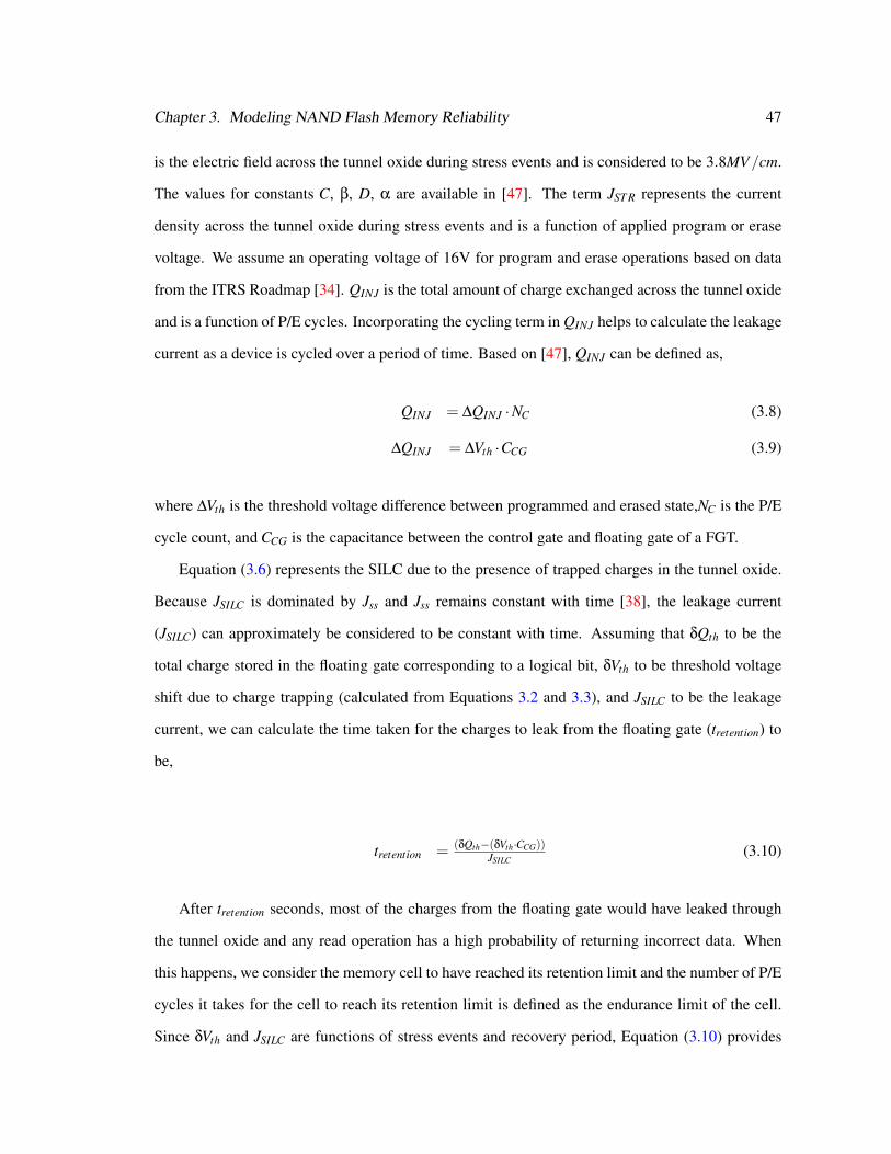
Chapter 3. Modeling NAND Flash Memory Reliability 47
is the electric field across the tunnel oxide during stress events and is considered to be 3.8MV/cm.
The values for constants C, β, D, α are available in [47]. The term JST R represents the current
density across the tunnel oxide during stress events and is a function of applied program or erase
voltage. We assume an operating voltage of 16V for program and erase operations based on data
from the ITRS Roadmap [34]. QINJ is the total amount of charge exchanged across the tunnel oxide
and is a function of P/E cycles. Incorporating the cycling term in QINJ helps to calculate the leakage
current as a device is cycled over a period of time. Based on [47], QINJ can be defined as,
QINJ = ∆QINJ ·NC (3.8)
∆QINJ = ∆Vth ·CCG (3.9)
where ∆Vth is the threshold voltage difference between programmed and erased state,NC is the P/E
cycle count, and CCG is the capacitance between the control gate and floating gate of a FGT.
Equation (3.6) represents the SILC due to the presence of trapped charges in the tunnel oxide.
Because JSILC is dominated by Jss and Jss remains constant with time [38], the leakage current
(JSILC) can approximately be considered to be constant with time. Assuming that δQth to be the
total charge stored in the floating gate corresponding to a logical bit, δVth to be threshold voltage
shift due to charge trapping (calculated from Equations 3.2 and 3.3), and JSILC to be the leakage
current, we can calculate the time taken for the charges to leak from the floating gate (tretention) to
be,
tretention = (δQth−(δVth·CCG))JSILC
(3.10)
After tretention seconds, most of the charges from the floating gate would have leaked through
the tunnel oxide and any read operation has a high probability of returning incorrect data. When
this happens, we consider the memory cell to have reached its retention limit and the number of P/E
cycles it takes for the cell to reach its retention limit is defined as the endurance limit of the cell.
Since δVth and JSILC are functions of stress events and recovery period, Equation (3.10) provides

Chapter 3. Modeling NAND Flash Memory Reliability 48
an estimate of data retention period in NAND flash memory after taking stress and recovery into
account.
3.4 Impact of Detrapping on Data Retention
Using the analytical model that we developed in the previous section, we analyze the impact of
recovery and detrapping on data retention. We examine when data retention related failures occur
and how recovery periods help in increasing data retention of flash. The results of this analysis
are shown in Figure 3.2a for SLC and Figure 3.2b for 2-bit MLC flash. These results use a flash
feature size of 80nm because the cell-level reliability measurements are available only for this tech-
nology node. These estimates are based on an operating temperature of 30◦C, the typical ambient
temperature of the storage system in datacenters [69].
Typically, OEM datasheets specify a retention period of at least 10 years for NAND flash. This
rating is usually very conservative and many supplementary documents provided by OEMs show
that the typical retention period is around 100 years for NAND flash memory that has undergone
very little cycling [62, 63]. Our results show that the data retention period of SLC based flash is
about 65 years (nearly 23 years for 2-bit MLC flash) for relatively small P/E cycle counts, which is
similar to datasheet estimates.
From Figures 3.2a and 3.2b, we can observe that, when there is no recovery between successive
cycles, the memory cell encounters retention failure when the total number of P/E cycles is around
100K for SLC flash and 10K for MLC flash, which concurs with the conservative values specified
in the datasheets. However, as the recovery period between successive stress events increases, the
number of times the cell can be cycled before retention failure occurs increases exponentially. Both
SLC and 2-bit MLC flash experience a steep drop in their retention period when they are subjected
to a few hundreds to thousands of cycles. For SLC flash, the retention period drops from about 65
years (for no recovery period) to about 20 years in a few hundred cycles, while in case of MLC flash,
the retention period drops from nearly 23 years (for no recovery period) to around 5 years in a few
thousand cycles. However, after this steep drop, the rate of decrease in the retention period slows
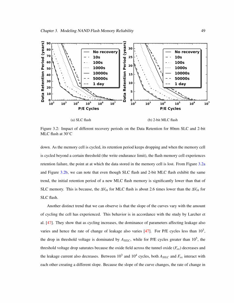
Chapter 3. Modeling NAND Flash Memory Reliability 49
102 103 104 105 106 107 108
P/E Cycles
0
10
20
30
40
50
60
70
80
90D
ata
Rete
ntio
n Pe
riod
(ye
ars)
No recovery10s100s1000s10000s50000s1 day
(a) SLC flash
102 103 104 105 106 107
P/E Cycles
0
5
10
15
20
25
30
Dat
a Re
tent
ion
Peri
od (
year
s)
No recovery10s100s1000s10000s50000s1 day
(b) 2-bit MLC flash
Figure 3.2: Impact of different recovery periods on the Data Retention for 80nm SLC and 2-bitMLC flash at 30◦C
down. As the memory cell is cycled, its retention period keeps dropping and when the memory cell
is cycled beyond a certain threshold (the write endurance limit), the flash memory cell experiences
retention failure, the point at at which the data stored in the memory cell is lost. From Figure 3.2a
and Figure 3.2b, we can note that even though SLC flash and 2-bit MLC flash exhibit the same
trend, the initial retention period of a new MLC flash memory is significantly lower than that of
SLC memory. This is because, the ∆Vth for MLC flash is about 2.6 times lower than the ∆Vth for
SLC flash.
Another distinct trend that we can observe is that the slope of the curves vary with the amount
of cycling the cell has experienced. This behavior is in accordance with the study by Larcher et
al. [47]. They show that as cycling increases, the dominance of parameters affecting leakage also
varies and hence the rate of change of leakage also varies [47]. For P/E cycles less than 103,
the drop in threshold voltage is dominated by ASILC, while for P/E cycles greater than 105, the
threshold voltage drop saturates because the oxide field across the tunnel oxide (Fox) decreases and
the leakage current also decreases. Between 103 and 104 cycles, both ASILC and Fox interact with
each other creating a different slope. Because the slope of the curve changes, the rate of change in

Chapter 3. Modeling NAND Flash Memory Reliability 50
102 103 104 105 106 107
P/E Cycles
10
20
30
40
50
60
70
80
90
Dat
a Re
tent
ion
Perio
d (y
ears
)
Impact of Temperature on Data Retention for 100s Recovery Period30 �C
35 �C
40 �C 45 �C 50 �C 55 � C
Figure 3.3: Impact of temperature on data retention for SLC flash with 100 seconds recovery period.
retention period also varies significantly with cycling.
3.5 Impact of Temperature on Data Retention
We use the Arrhenius equation to study the effect of temperature on flash reliability. As our objec-
tive is to study the reliability of SSDs in data center environment, we choose a variety of tempera-
tures ranging from 30◦C to 55◦C, which is the typical operating temperature range in data centers.
The temperature ranges are representative of the typical operating temperature for disks in data cen-
ters [69, 82]. The baseline results were obtained by setting Tuse to 30◦C, which is a typical ambient
temperature at which disks operate in data centers.
Based on industry standards like JEDEC, the activation energy for data retention is considered
to be 0.3eV [40]. Figure 3.3 and Figure 3.4 illustrate the change in retention period as temperature
increases from 30◦C to 55◦C. while the recovery period is kept constant at 100 seconds. With the
data retention activation energy set at 0.3eV and the detrapping activation energy set at 1.1eV , when
the operating temperature increases from 30◦C to 35◦C the time to failure (the data retention period)
reduces by 18% causing the chip to become less reliable. Thus temperature has a major impact on
Chapter 3. Modeling NAND Flash Memory Reliability 51
102 103 104 105
P/E Cycles
5
10
15
20
25
30
35
Dat
a Re
tent
ion
Perio
d (y
ears
)
Impact of Temperature on Data Retention for 100s Recovery Period30 �C
35 �C
40 �C 45 �C 50 �C 55 � C
Figure 3.4: Impact of temperature on data retention for 2-bit MLC flash with 100 seconds recoveryperiod.
the reliability of flash memory. These results can be used to estimate how flash memory operates at
various temperature points and the expected endurance and retention at these temperatures.
It should be noted that even though charge detrapping increases with temperature (due to higher
activation energy), temperature has a negative effect on the overall reliability of flash. Proposal like
[71] try to exploit detrapping at higher temperature by heating the SSDs to high temperatures. As
our results show, the problem with this approach is that while such techniques increase detrapping,
they also increase SILC, resulting in reduced retention period. Because temperature is a important
parameter that affects silicon and SSD reliability, both SSD architects and system administrators
have a critical role to play. The cooling choices adopted by system administrators to control the
ambient temperature of servers can have a significant impact on the reliability of SSDs. Similarly,
SSD architects can influence the reliability of SSDs by placing temperature sensors inside SSDs
that can be used to monitor and control their reliability.
Figures 3.2a and 3.2b show that there is clear tradeoff between the data retention and the en-
durance of flash memory. If the data retention for NAND flash can be relaxed linearly, the total
number of P/E cycles possible can be increased exponentially. For example, in the case of 2-bit

Chapter 3. Modeling NAND Flash Memory Reliability 52
MLC flash having an average recovery period of about 10,000 seconds, the P/E cycle count can be
increased from 10000 to 52,800 when the data retention period requirement is be reduced from 10
years to 5 years.
These results indicate that there is a tradeoff between endurance and data retention for both
SLC and MLC flash that can be exploited by storage systems to optimize either of these metrics. In
Chapter 4, we show how to tradeoff of data retention to increase the endurance of MLC flash based
SSDs.
3.6 Related Work
There are several transistor-level studies on charge trapping and detrapping of flash that have shown
the benefit of benefit of recovery periods in improving NAND flash endurance and data retention
[55, 103, 104]. The effect of temperature on interface trap generation in CMOS transistors have
been theorized using concepts like Negative Bias Temperature Instability (NBTI) and Positive Bias
Temperature Instability (PBTI). Similar to recovery due to detrapping in Floating Gate Transistors,
traps in CMOS transistors can be removed by applying voltage bias to the transistor terminals
during runtime [3, 46, 85, 94]. Mohan et al. propose leveraging these properties at the architecture
level to boost endurance [60]. Wu et al. propose to accelerate the recovery process using heat [71],
although heat-assisted detrapping leads to data loss and therefore requires data to be backed up and
reloaded into flash based storage devices after heating.
3.7 Summary
In this chapter, we have presented a detailed analytical model to understand data retention based
NAND flash failure mechanism. We use the model to quantify the impact of recovery period and
temperature on data retention. We show that recovery periods can significantly boost the data
retention of NAND flash based memories and is an important parameter to be considered for opti-
mization. We also show that high temperatures negatively impact NAND flash data retention due to

Chapter 3. Modeling NAND Flash Memory Reliability 53
increase in Stress Induced Leakage Current (SILC). The relationship between temperature and data
retention is modeled using an Arrhenius equation with an activation energy of 0.3EV .

Chapter 4
Building High Endurance, Low Cost SSDs for Datacenters
4.1 Introduction
As large enterprises move to the cloud, they host online services and store consumer data in large
scale datacenters across the world. Moving consumer data to the cloud increases the demand for
both storage capacity and performance. Storage accounts for a significant portion of the Total Cost
of Ownership (TCO) and contributes upto 30% of the total power consumption in a datacenter [20].
This number is projected to become more significant given the uptrend in user data being stored
on the cloud. IDC reports that user data stored in datacenters has been growing at an exponential
rate [21]. Given the increasing demand, the cost of designing storage is expected to increase sig-
nificantly. In order to keep pace with increasing data growth, enterprises are forced to look for new
storage technologies that can achieve performance and capacity requirements at an optimal cost.
Solid State Drives (SSDs) have become increasingly relevant for datacenter storage since they
achieve these objectives. The $/GB of flash based devices has been dropping steadily, making
them attractive for use in large scale storage systems. SSDs offer several advantages including
lower power and higher performance when compared to hard disk drives that were the traditional
storage medium in large datacenters. Since enterprise workloads are mostly random in nature [75],
they benefit significantly from the superlative random I/O performance of SSDs. Large datacenters
hosting online services, such as Web Search, OLTP, and Cloud services employ SSDs as main
memory extension buffers, Hard Disk Drive (HDD) caching solutions in the storage hierarchy, and
54

Chapter 4. Building High Endurance, Low Cost SSDs for Datacenters 55
sometimes as actual HDD replacements. Flash memory comes in three flavors - (i) Single Level
Cell (SLC), (ii) Multi-Level Cell (MLC), where multiple bits are stored per memory cell, and (3)
Enterprise MLC (eMLC). SLC provides the highest performance, but is the most expensive and
least dense of all three types. MLC provides the lowest cost and highest density, albeit at a lower
performance than SLC. However, MLC is still a strong performance value proposition compared
to HDDs, since HDD performance is still significantly lower than MLC flash. eMLCs are MLC
based devices with additional firmware and ECC geared towards enterprise class customers but at
higher cost than MLC [65]. In a datacenter scale system, a key figure-of-merit is the the ratio of the
cost of the SSD to the cost of the overall server solution without SSDs. It is important to minimize
this ratio in order to be able to deploy SSDs at a large scale in a cost-effective manner. Figure 4.1
presents this ratio for the three types of flash SSDs for both commodity and enterprise class servers
whose configurations are shown in the table. The cost prices for the servers and SSDs are obtained
from list prices available online [6]. As we can see, among the three types of flash, MLC is clearly
the best in terms of the SSD:Server cost ratio for both commodity and enterprise servers.
In this chapter, we evaluate MLC based solutions, given its performance and cost benefits.
However, the major impediment in adopting MLC SSDs at datacenter scale has been the endurance
limitation. Enterprise storage has to support significant write traffic, when compared to client or
desktop storage. This requirement directly impacts the endurance limits of flash technology. Flash
memory blocks can wear out after a certain number of write (program) and erase operations, a
property referred to as limited write endurance. Typical enterprise servers are designed to be cost-
amortized for a period of 3-5 years based on the respective TCO model that an enterprise adopts.
Based on this expected lifetime, replacement and service costs are projected to be 15% of the overall
server infrastructure cost [98]. Hence, increasing the cost of the server due to costly SSD replace-
ments impacts the financial bottom line of a large enterprise. If the write endurance limit is reached
before the expected TCO lifetime of a server, then this results in a significant cost to the enterprise.
In a cloud environment, where efficiency of operation is key to revenue margins, failures due to
write endurance limitations need to be avoided. Hence there is a need for a flash device that is
cost optimal and provides all the benefits of flash technology, but at the same time, does not have
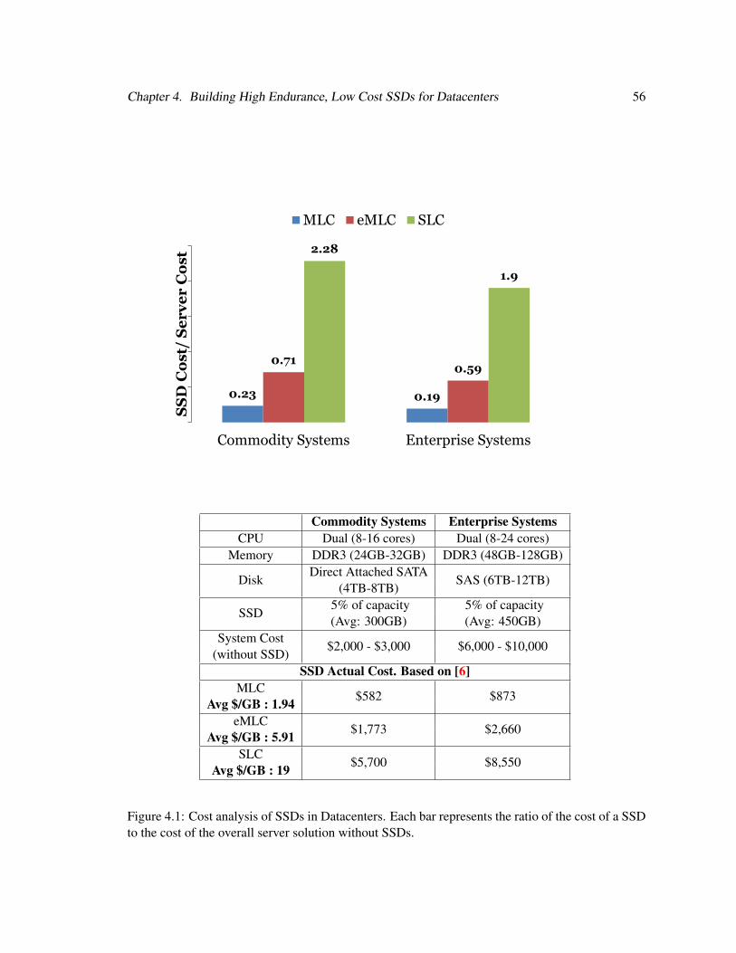
Chapter 4. Building High Endurance, Low Cost SSDs for Datacenters 56
0.23 0.19
0.71 0.59
2.28
1.9
Commodity Systems Enterprise Systems
SS
D C
os
t/ S
er
ve
r C
os
t
MLC eMLC SLC
Commodity Systems Enterprise SystemsCPU Dual (8-16 cores) Dual (8-24 cores)
Memory DDR3 (24GB-32GB) DDR3 (48GB-128GB)
DiskDirect Attached SATA
SAS (6TB-12TB)(4TB-8TB)
SSD5% of capacity 5% of capacity(Avg: 300GB) (Avg: 450GB)
System Cost$2,000 - $3,000 $6,000 - $10,000
(without SSD)SSD Actual Cost. Based on [6]
MLC$582 $873Avg $/GB : 1.94
eMLC$1,773 $2,660Avg $/GB : 5.91
SLC$5,700 $8,550Avg $/GB : 19
Figure 4.1: Cost analysis of SSDs in Datacenters. Each bar represents the ratio of the cost of a SSDto the cost of the overall server solution without SSDs.

Chapter 4. Building High Endurance, Low Cost SSDs for Datacenters 57
the disadvantage of limited write endurance. While, among the three flash technologies, MLC has
the lowest SSD:Server cost ratio, it is also the one that has the least amount of endurance. The
key objective of this chapter is to demonstrate how we can leverage MLC based NAND flash in
datacenters while boosting its endurance. We use the reliability model developed in Chapter 3 to
build high endurance SSDs by trading off data retention. To ensure that sacrificing data retention
does not violate the integrity of the stored data, we propose that the flash memory cells be periodi-
cally refreshed and we evaluate the performance and reliability impact of implementing an Earliest
Deadline First (EDF) based refresh policy within the SSD for a set of datacenter workloads.
The rest of the chapter is organized as follows: Section 4.2 describes the experimental setup
while Section 4.3 describes how we simulate Enterprise SSDs using Hard-Disk Drives (HDDs)
based workload traces. In Section 4.4, we propose a new methodology to evaluate SSD lifetime
over long time periods (in the order of years), while Section 4.5 explains the benefits of the EDF
based refresh policy on the reliability of MLC based SSDs. Chapter 4.6 presents the related work
and Chapter 4.7 summarizes this work.
4.2 Experimental Methodology
In this section we describe our experimental methodology for analyzing SSD performance and
reliability.
4.2.1 SSD Configuration and Simulator Setup
As our objective is to evaluate the reliability of MLC in datacenters, we simulate a 64GB 2-bit
MLC based SSD (M-SSD) similar to [31]. M-SSD uses a wear-aware cleaning algorithm and
uses free blocks within a memory chip for wear leveling (allocation pool granularity of a chip) as
mentioned in [5]. M-SSD has a spare area of 10% and also supports internal plane level copy back
operations to leverage plane-level parallelism available inside SSDs. We use Disksim, a widely used
trace driven simulator for studying storage systems, augmented with with an SSD model developed

Chapter 4. Building High Endurance, Low Cost SSDs for Datacenters 58
Workload Trace Total Read & RequestDuration I/Os Write Inter-Arrival(hours) (millions) ratio average(ms)
Display Ads24 1.09 1:1.22 79.63Platform Payload
Server (DAPPS)Exchange Server
24 5.50 1:2.22 15.79(Exchange)MSN File
6 2.22 1:1.24 9.78Server (MSNFS)MSN Metadata
6 0.52 1:0.64 41.63Server (MSNCFS)
Table 4.1: Properties of Enterprise Workloads Used for Evaluation.
by Microsoft [5]. We incorporate our analytical reliability model developed in Section 3.3 into
Disksim.
4.2.2 Workloads
Our workloads consist of block-level I/O traces collected from production systems in Microsoft
that use HDD-based storage and are available publicly [75]. These workloads are summarized in
Table 4.1 and correspond to the Logical Unit (LUN) with the highest write traffic. Each workload
trace consists of millions of I/O requests corresponding to many hours of usage, span over several
terabytes of I/O address range, and spread across many Logical Units (LUNs). As program and
erase operations have the highest impact on flash reliability, we choose the LUN with the highest
write traffic for our analysis.
4.3 Simulating SSDs with HDD Workload Traces
Since SSD performance is much higher than that of an HDD, a storage system where HDDs are
replaced by SSDs will be expected to be more responsive and can absorb higher amounts of I/O
traffic. Therefore, analyzing SSD behavior using HDD traces can lead to inaccurate assessments.
There are two alternatives to address this problem. One approach is to use closed-loop simulation,
where we recreate the entire computing infrastructure on which the traces were collected to assess

Chapter 4. Building High Endurance, Low Cost SSDs for Datacenters 59
the I/O behavior when the HDDs are replaced by SSDs. Another alternative approach is to use I/O
traces that were collected on SSD-based storage. Unfortunately, neither option is possible for us
since we do not have access to datacenter systems on which the traces were collected and there are
no publicly available SSD I/O traces.
In this chapter, we approximate the behavior of the existing HDD traces on SSDs using the
methodology proposed by Delimitrou et al. [15], who considered the problem of generating SSD
traces from a HDD trace for datacenter workloads. They showed that the inter-arrival time between
I/O requests is a key parameter that needs to be considered when generating an SSD trace. Since an
SSD can handle much higher I/O loads, we shorten the inter-arrival times between the I/O requests,
while preserving all the other properties of the workload trace, such as the spatial distribution, the
ratio of reads and writes, and the distribution of request sizes. We use a scaling factor for the inter-
arrival time such that the SSD can handle the increase in traffic without being over-utilized. To
define over-utilization, we first define performance. Performance is defined as the response time
of the SSD for the 80th percentile of the I/O requests in the higher intensity workload, normalized
to the response time of the 80th percentile of the requests in the original HDD workload trace. We
define over-utilization to be the region where the Normalized Response Time (NRT) at the 80th
percentile is greater than 3, which we find is the point when the bandwidth of the SSD has been
exhausted and consequently the SSD begins to show a clear degradation in performance for our
scaled workloads.
Figure 4.2 plots the variation in the NRT as the intensity of the workload is gradually increased.
The area above the horizontal line in the Figure indicates the over-utilization region. We observe
that each workload reaches over-utilization at a different intensity. For Exchange, DAPPS and
MSNFS, M-SSD reaches the over-utilization region when the intensity increases beyond 4, 10 and
7 respectively. Hence, for Exchange, DAPPS and MSNFS we choose acceleration factors of 4,10,
and 7 respectively. For MSNCFS, the NRT does not change even when the intensity increases to
15. As shown in Table 4.1, the I/O intensity of MSNCFS is so low that even at 15X intensity, the
response time at the 80th percentile does not change. Therefore, we choose an acceleration factor of
15 for MSNCFS. For the rest of this chapter, we denote these modified higher intensity workloads

Chapter 4. Building High Endurance, Low Cost SSDs for Datacenters 60
0 2 4 6 8 10 12 14Intensity
0
2
4
6
8
10
NRT
at
80 th
per
cent
ile
Over-utilization region
DAPPSExchangeMSNFSMSNCFS
Figure 4.2: Impact of Varying Workload Intensity on SSD Response Time
as SSD-EXCH,SSD-DAPPS, SSD-MSNFS and SSD-MSNCFS while using them for analysis.
4.4 Estimating SSD Lifetime Over Long Timescales
Since SSD reliability issues manifest over a period of many years and TCO considerations also
span 3-5 year time horizons, our analysis needs to span such time periods. In order to carry out
such an analysis, we can replay the workload traces, which span several hours to a day’s worth
of I/O activity, repeatedly over a multi-year timescale. However, running a simulation of an I/O
intense workload over such a long time period requires several weeks of simulation time and is
therefore prohibitively expensive. All our high-intensity workloads except SSD-MSNCFS are very
I/O intense and therefore suffer from these excessively long simulation times. In order to tackle
this problem, we use a statistical approach to reduce the simulation time for SSD-EXCH, SSD-
DAPPS, and SSD-MSNFS, and perform a detailed simulation of SSD-MSNCFS. We now describe
our statistical approach.

Chapter 4. Building High Endurance, Low Cost SSDs for Datacenters 61
For each workload, we run a detailed simulation in Disksim using the baseline HDD workload
trace as well as some high intensity versions of the trace over a multi-year timescale. We choose this
timescale to be 5 years. After simulating every 15 days worth of I/O activity, a snapshot containing
the lifetime of all the blocks in the SSD is obtained. Each snapshot contains the δVth, the P/E cycles,
and the retention period of every block in the SSD.
We found that over this 5-year time period, the retention period of blocks in the SSD are nor-
mally distributed for MSNFS and DAPPS. Exchange had bimodal normal distribution due to a
skewed spatial distribution of requests in flash chips 7 and 8 and hence those chips were wearing
out faster than the other chips in the SSD. However, most importantly, irrespective of the inten-
sity and time at which the snapshot was obtained, the type of the distribution remained the same.
Because the type of the distribution is found to be independent of intensity and time at which the
snapshot is obtained, determining the lifetime of blocks at a higher intensity and at a particular time
requires us to estimate the mean and standard deviation of block lifetime distributions for MSNFS
and DAPPS, while for Exchange, we need to estimate two means and two standard deviations cor-
responding to the bimodal normal distribution. (Bimodal normal distribution has a 5th parameter,
p, that indicates the ratio of the area of the two normal distributions. We do not estimate this
parameter, because p remains constant across all simulations.)
For each workload, let St,i denote the snapshot at time t for intensity i. As snapshots are stored
for every 15 days of simulated I/O activity, 1 <= t <= 120 (snapshots are taken every 15 days for
60 months - a total of 120 snapshots). Because simulation time increases as intensity increases,
we could not run detailed simulations with the same intensity for every workload. For Exchange,
snapshots corresponding to detailed simulation were obtained for i = 1 and i = 2, while for DAPPS,
MSNFS, snapshots were obtained for i = 1 to i = 5. In order to get the distribution of retention
period for all blocks in the SSD for SSD-MSNFS (i = 7) and SSD-DAPPS (i = 10), we need to
estimate two parameters, while for SSD-EXCH (i = 4), we need to estimate four parameters at
various time intervals. For each parameter to be estimated, we use the following approach. We
use regression on a subset of data from the snapshots to obtain a curve that fits the data. Since
it is possible to fit the data with more than one curve, we choose the curve that has the least root
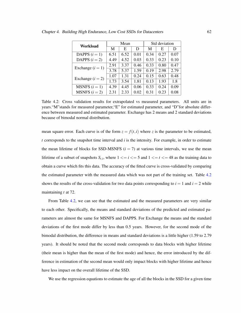
Chapter 4. Building High Endurance, Low Cost SSDs for Datacenters 62
Workload Mean Std deviationM E D M E D
DAPPS (i = 1) 6.51 6.52 0.01 0.34 0.27 0.07DAPPS (i = 2) 4.49 4.52 0.03 0.33 0.23 0.10
Exchange (i = 1)2.91 3.37 0.46 0.33 0.80 0.473.78 5.37 1.59 0.19 2.98 2.79
Exchange (i = 2)1.07 1.31 0.24 0.15 0.63 0.481.73 3.54 1.81 0.13 1.93 1.8
MSNFS (i = 1) 4.39 4.45 0.06 0.33 0.24 0.09MSNFS (i = 2) 2.31 2.33 0.02 0.31 0.23 0.08
Table 4.2: Cross validation results for extrapolated vs measured parameters. All units are inyears.“M”stands for measured parameter,“E” for estimated parameter, and “D”for absolute differ-ence between measured and estimated parameter. Exchange has 2 means and 2 standard deviationsbecause of bimodal normal distribution.
mean square error. Each curve is of the form z = f (t, i) where z is the parameter to be estimated,
t corresponds to the snapshot time interval and i is the intensity. For example, in order to estimate
the mean lifetime of blocks for SSD-MSNFS (i = 7) at various time intervals, we use the mean
lifetime of a subset of snapshots St,i, where 1 <= i <= 5 and 1 <= t <= 48 as the training data to
obtain a curve which fits this data. The accuracy of the fitted curve is cross-validated by comparing
the estimated parameter with the measured data which was not part of the training set. Table 4.2
shows the results of the cross-validation for two data points corresponding to i = 1 and i = 2 while
maintaining t at 72.
From Table 4.2, we can see that the estimated and the measured parameters are very similar
to each other. Specifically, the means and standard deviations of the predicted and estimated pa-
rameters are almost the same for MSNFS and DAPPS. For Exchange the means and the standard
deviations of the first mode differ by less than 0.5 years. However, for the second mode of the
bimodal distribution, the difference in means and standard deviations is a little higher (1.59 to 2.79
years). It should be noted that the second mode corresponds to data blocks with higher lifetime
(their mean is higher than the mean of the first mode) and hence, the error introduced by the dif-
ference in estimation of the second mean would only impact blocks with higher lifetime and hence
have less impact on the overall lifetime of the SSD.
We use the regression equations to estimate the age of all the blocks in the SSD for a given time

Chapter 4. Building High Endurance, Low Cost SSDs for Datacenters 63
and workload intensity. We then sample the multi-year timescale that we are interested in studying
by choosing several points in time over this timescale. We then run a short duration (1 hour) detailed
simulation in Disksim from each such instant to determine the impact of aging on performance for
each of the workloads that use the extrapolation.
4.5 Impact of SSD Workloads on MLC Flash Reliability
In this section we analyze the impact of SSD enterprise workloads on the reliability of M-SSD.
We begin by defining the metrics that we use for evaluation, then analyze the retention time vs.
endurance characteristics for the workloads, and then evaluate the refresh policy.
4.5.1 Metrics
To quantify lifetime, we use the virtual retention period as the metric. The virtual retention period
is defined as the minimum time duration for which any data written in the SSD can be read success-
fully. SSDs can have different virtual retention period requirements depending on the application
for which they are used. If the SSDs cannot store data for the specified virtual retention period they
are considered to be unreliable. Typical virtual retention period requirement for applications vary
from 3 months to 1 year [39]. For the baseline analysis, we consider the SSD to be unusable if the
actual data retention period of blocks drops below the virtual retention period. By using a range
of virtual retention period thresholds (1 year, 6 months, 3 months and 1 month), we analyze the
reliability of SSD over a variety of usage scenarios.
Since different blocks in the SSD can have different retention periods, we use the retention
period at the 10th percentile of all blocks as the criteria for our evaluation. We chose the 10th
percentile because, the over-provisioning capacity of M-SSD is 10% and the SSD is still functional
as long as the amount of free space in the drive is more than 10%. Hence, we consider the SSD
to be completely unusable when the data retention period of 10% of blocks falls below the virtual
retention period threshold. As mentioned in Section 4.2, we use the normalized response time of
the 80th percentile of the total number of requests as the performance metric.
Chapter 4. Building High Endurance, Low Cost SSDs for Datacenters 64
4.5.2 Baseline Evaluation
In Figure 4.3, we show the impact of SSD workloads on MLC SSD reliability. Our objective is to
determine if our MLC SSD (M-SSD) is capable of servicing enterprise workloads over the service
life. If not, we use our results to determine when the M-SSD needs to be replaced. The x-axis in the
figure represents the period of simulation which extends upto 5 years (or 60 months) while the y-
axis is the retention period at the 10th percentile. The various dotted horizontal lines parallel to the
x-axis indicate different virtual retention period thresholds. The curves in the Figure 4.3 are similar
to the curves in Figure 3.2b, except that the y-axis is in log-scale. While the data in Figure 3.2b is for
a single flash memory cell under controlled stress-recovery conditions, the data in Figure 4.3 also
takes into account the workload behavior, SSD architecture, and the FTL. Hence, the points in the
curve where their slopes change are different for different workloads. From Figure 4.3, we can see
that SSD-EXCH, SSD-DAPPS and SSD-MSNFS have a significant impact on the reliability of M-
SSD. For these workloads, the lifetime of baseline M-SSD crosses the virtual retention threshold
of 1 year within 20 months of actual usage, thereby requiring multiple replacements within the
TCO lifetime of the server (3-5 years). With lower virtual retention period thresholds, the usage
time of the SSD increases, but this can still be improved further. Our objective is to delay the SSD
replacements as long as possible, ideally beyond the TCO lifetime. The only exception to this trend
is SSD-MSNCFS, whose impact on the lifetime of M-SSD is modest. Even after 5 years of use,
the retention period of blocks in M-SSD is more than 3 years, indicating that the write traffic in
the SSD is not sufficient enough to stress the SSD. Hence, we exclude SSD-MSNCFS from further
consideration in our experiments.
It should be noted that these results take into account the stress and the recovery patterns that
M-SSD experiences over its usage period. While our analysis in Section 3.4 showed that recovery
periods increase the retention (and thereby the endurance) of the SSDs, these results indicate that
even with the benefit of recovery periods, M-SSD cannot be used for the entire 5-year timescale for
some enterprise workloads. These results were obtained after enabling state-of-the-art wear level-
ing optimizations like hot-cold data swap and rate-limited wearout in M-SSD [5], indicating that
these existing optimizations are not sufficient to extend the usability of the SSD over the timescale.
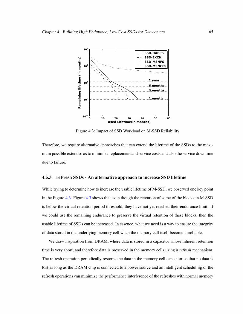
Chapter 4. Building High Endurance, Low Cost SSDs for Datacenters 65
0 10 20 30 40 50 60Used Lifetime(in months)
10-1
100
101
102
103
Rem
aini
ng li
feti
me
(in
mon
ths)
1 year6 months3 months
1 month
SSD-DAPPSSSD-EXCHSSD-MSNFSSSD-MSNCFS
Figure 4.3: Impact of SSD Workload on M-SSD Reliability
Therefore, we require alternative approaches that can extend the lifetime of the SSDs to the maxi-
mum possible extent so as to minimize replacement and service costs and also the service downtime
due to failure.
4.5.3 reFresh SSDs - An alternative approach to increase SSD lifetime
While trying to determine how to increase the usable lifetime of M-SSD, we observed one key point
in the Figure 4.3. Figure 4.3 shows that even though the retention of some of the blocks in M-SSD
is below the virtual retention period threshold, they have not yet reached their endurance limit. If
we could use the remaining endurance to preserve the virtual retention of these blocks, then the
usable lifetime of SSDs can be increased. In essence, what we need is a way to ensure the integrity
of data stored in the underlying memory cell when the memory cell itself become unreliable.
We draw inspiration from DRAM, where data is stored in a capacitor whose inherent retention
time is very short, and therefore data is preserved in the memory cells using a refresh mechanism.
The refresh operation periodically restores the data in the memory cell capacitor so that no data is
lost as long as the DRAM chip is connected to a power source and an intelligent scheduling of the
refresh operations can minimize the performance interference of the refreshes with normal memory
Chapter 4. Building High Endurance, Low Cost SSDs for Datacenters 66
access operations. We apply this notion of a refresh to Flash memory, wherein the data in SSD
blocks whose lifetime falls below the virtual retention threshold are refreshed, thereby increasing
the usable lifetime of blocks. We call our SSD that use these refresh operations as reFresh-SSD.
Refreshing an SSD involves periodically checking all blocks in the SSD and moving data from
less reliable blocks to more reliable blocks to match the reliability constraints of the application.
Thus, a refresh operation involves a read operation of a less reliable block and a program operation
to a more reliable block. Since a refresh operation is a combination of read and program operations,
the only change required to support them in SSDs is to change the FTL software to initiate these
operations whenever required and does not require any change to the hardware of the SSD or the
flash memory chips. Refresh operations are different from wear leveling operations. Both move
data across SSD blocks. But, refresh operations are triggered by the FTL when it senses that the
lifetime of blocks containing data falls below some threshold (based on the application’s require-
ment). Hence, refresh operations are triggered due to an immediate deadline, while wear leveling
operations are triggered in order to achieve the long term objective of evening the wearout across
blocks. The latency of a refresh operation can be significant, as it involves reading and writing all
valid pages in the block. For M-SSD, this means that the latency of a refresh operation is 128 times
the sum of read and write latency. Therefore, it is imperative to intelligently schedule the refresh
operations so that the performance impact on normal I/O operations is minimized.
Since the need to refresh a block can be viewed as an operation that needs to be completed
within a specific deadline to meet the virtual retention time requirement, we evaluate a refresh
policy that is based on the Earliest Deadline First (EDF) scheduling algorithm. In this approach,
the state of those blocks that contain valid data and whose lifetime is less than the virtual retention
period threshold is maintained in a queue called the refresh queue. This queue is a priority queue
where blocks with the lowest lifetime are at the head. Dequeue operations always begin at the head
of the queue. The block with the least retention period is assigned the highest priority for the next
refresh operation. Since flash does not support in-place updates, a target block needs to identified
to move the contents of the block to be refreshed. To identify the target block, we use the wear
leveling algorithm in the FTL to determine a free block with the highest remaining lifetime. At
Chapter 4. Building High Endurance, Low Cost SSDs for Datacenters 67
every refresh interval r, the FTL checks the refresh queue, picks all those blocks that need to be
refreshed (refresh blocks) based on their deadline, identifies a free target block for each refresh
block, copies the contents of refresh block to the target block, and finally erases the refresh block.
The FTL invokes garbage collection if the number of free blocks in the SSD becomes low. In this
way, even if the lifetime of a block is less than the virtual retention period, the data in the block is
periodically refreshed to ensure their integrity.
Unlike traditional approaches that seek to reduce the write traffic into the SSD to increase
the lifetime of SSDs, refresh operations actually increase the write traffic due to additional write
operations. While this may seem counterintuitive, it should be noted that refresh operations help
the FTL exploit the remaining endurance in the SSD blocks instead of ignoring them just because
their lifetime is below an application determined threshold. Even though this involves additional
write activity, it increases the longevity of the SSD upto a certain lifetime (which is higher than
the baseline) until these additional write operations themselves decrease the lifetime of blocks in
the SSD. We soon reach a point in time where the SSD spends a majority of the time refreshing its
blocks, thereby heavily interfering with normal I/O operations of the workload and causing severe
degradation in SSD performance. At this point, the SSD becomes practically unusable.
Figures 4.4a to 4.4d show the benefit of using the EDF based refresh policy on the reliability
of the SSD for the various workloads at different virtual retention period thresholds. The x-axis
in these figures represent the usage time while the y-axis represents the normalized response time
over the usage period (lower is better). These results were obtained by running simulations upto
the point where the performance of reFresh SSDs is equal to the end-of-life performance of the
baseline SSDs (without refresh). Beyond this point, a significant amount of time is spent by the
SSD is maintaining its state, instead of servicing the I/O requests of the workload. From these
figures, we can make the following important observations:
1. Without refresh operations, SSDs with virtual retention thresholds of either 1 year or 6
months can be used for a maximum of 23 months (6-month virtual retention period for SSD-
DAPPS). With refresh, the usage lifetime of the SSD can be extended to upto 36 months. The
increase in lifetime varies from 23% for SSD-MSNFS to 56% to SSD-DAPPS.

Chapter 4. Building High Endurance, Low Cost SSDs for Datacenters 68
0
1
2
3
4
5
6
0 5 10 15 20 25 30 35 40 45
NR
T a
t 8
0th
pe
rc
en
tile
Usage time (in months)
SSD-DAPPS - No Refresh
SSD-Dapps - EDF
SSD-EXCH - No Refresh
SSD-EXCH - EDF
SSD-MSNFS - No Refresh
SSD-MSNFS - EDF
(a) Virtual retention period - 1 year
0
1
2
3
4
5
6
0 5 10 15 20 25 30 35 40 45
NR
T a
t 8
0th
pe
rc
en
tile
Usage time (in months)
(b) Virtual retention period - 6 months
0
1
2
3
4
5
6
0 5 10 15 20 25 30 35 40 45
NR
T a
t 8
0th
pe
rc
en
tile
Usage time (in months)
(c) Virtual retention period - 3 months
0
1
2
3
4
5
6
0 5 10 15 20 25 30 35 40 45
NR
T a
t 8
0th
pe
rc
en
tile
Usage time (in months)
(d) Virtual retention period - 1 month
Figure 4.4: Impact of EDF Refresh Algorithm On the Lifetime of M-SSD

Chapter 4. Building High Endurance, Low Cost SSDs for Datacenters 69
2. For SSDs with lower virtual retention thresholds of 3 months and 1 month, the usage lifetime
without refresh operations is a maximum of 26 months, while with refresh operations, the
usage time increases to 38 months. The increase in lifetime varies from 6% for SSD-EXCH
to 42% for SSD-DAPPS.
3. Reducing the virtual retention period requirement diminishes the gain in lifetime because the
margin of lifetime for blocks is already becoming lower for lower virtual retention periods
and blocks begin to become unusable within a relatively short time period.
4. With refresh operations, performance of the SSD varies with time. Even after the SSD crosses
the baseline lifetime, there is a significant time period where refresh operations have very
little impact on the performance of SSDs. This is because the lifetime of blocks is relatively
high such that the number of refresh operations are performed infrequently. However, as the
blocks in the SSD reach their physical reliability limit, the performance starts to degrade. We
can observe that the normalized response time remains at 1 for some duration of time before
starting to increase sharply and soon reaches the response time of the baseline case.
5. The benefit of refresh operations directly correlate to the intensity of the write traffic in the
workloads. Workloads with lower write traffic (e.g. SSD-DAPPS) cause the SSD to fail
at a later point in time and the rate at which the blocks fail is also slower compared to the
more write-intense workloads. For those workloads where the rate at which blocks fail is
low, fewer refresh operations are scheduled over any given interval of time. Therefore, the
performance overheads imposed by these refreshes are also lower for those workloads.
In Figures 4.4a to 4.4d, we can observe that the duration between when the device is starting
to fail (performance starting to degrade) and has completely been rendered unusable is in the order
of a couple of months for all the workloads. This is because the wear leveler in the FTL tries to
even the wearout of the flash and hence the standard deviation in the lifetime of blocks in the SSD
is low. This behavior does not change with the inclusion of refresh operations because the wear
leveler does not change its function.

Chapter 4. Building High Endurance, Low Cost SSDs for Datacenters 70
Overall, we find that periodically refreshing the contents of an SSD is an effective way of
leveraging the tradeoff between endurance and retention time to increase the usable lifetime of
the SSD. Compared to the baseline case (no refresh), refresh operations allow SSDs to operate
for extended periods of time with minimal performance impact. Hence, they can help reduce the
number SSD replacements over the TCO period of the server infrastructure.
4.6 Related Work
Many architecture and software level techniques have been proposed to improve the reliability
of flash based SSDs. These include the use of hybrid HDD-SSD storage devices [89, 105], FTL
optimizations [24], and the use of parity codes across a RAID of SSDs [43]. Content aware tech-
niques that examine data patterns and reduce the number of write operations have also been pro-
posed [13,25]. Arpaci-Dusseau et al. propose a new interface called nameless writes that allows the
device to control actions like wear-leveling while obviating the need for large tables [8]. A recent
paper by Smullen et al. applied the idea of refresh to another non-volatile memory - STT-RAM -
where they use memory cells that are designed to provide very low retention times, which provide
improved performance and energy-efficiency for that memory technology when used for micropro-
cessor caches [87]. To the best of our knowledge, this dissertation is the first to leverage the tradeoff
between retention time and endurance and propose the use of refreshes to boost flash endurance.
Gaining a deep understanding of flash reliability has recently become a topic of great interest
in the architecture and systems communities. There have been recent flash chip characterization
studies that have shown that the endurance of flash memory chips is significantly higher than those
given in datasheets [16, 23]. There has also been a field-data analysis study from Fusion-IO on the
endurance, read disturbs, and data retention of SSDs in datacenters [26]. Recent research efforts
like [68, 74] have explored the benefits of relaxing flash retention to increase SSD performance.
While this chapter also examines the tradeoffs involved in relaxing flash retention, we focus our
effort on increasing flash endurance instead of flash performance. Our evaluation of flash reliability
is more realistic than [68,74] as our model considers the impact of recovery period on data retention

Chapter 4. Building High Endurance, Low Cost SSDs for Datacenters 71
and endurance.
4.7 Summary
SSDs can provide large performance and power benefits for datacenter storage. However, the lim-
ited endurance of flash memory needs to be addressed before SSDs can be practical for datacenter
workloads. We have shown that the endurance of flash can be boosted if one can sacrifice retention
time and that the reduction in the retention time can be offset by refreshing the data in the flash
memory cells. We have shown that such refresh policies can significantly extend the usability of the
SSD. Our future work in this area will be to explore other refresh policies, evaluate their implemen-
tation overheads within the flash controllers, and also study how refresh can be used in conjunction
with other reliability techniques to boost SSD reliability in datacenters.

Chapter 5
Architecting Petabyte Scale SSDs
5.1 Introduction
Over the past few years, enterprises across the world have rapidly been adopting NAND flash
based Solid State Disks (SSDs) to meet the demand for high capacity and high performance storage
systems. With the cost ($/GB) of NAND flash dropping steadily, SSDs have become more attractive
and are being used across all storage tiers in the data center [19]. NAND flash technology scaling
has ensured that the $/GB of SSDs will continue its decline for the near future [36]. In the past 10
years, flash storage device capacity has increased by a factor of 1000 (128MB in 2004 to 128GB
in 2014) [22]. With costs declining steadily, SSD capacities have continued to scale and current
enterprise SSDs have crossed the terabyte limit. As this scaling trend continues, we can envision a
future where SSD capacities approach the petabyte limit.
NAND is successfully transitioning from 2D to 3D to continue memory scaling and major
NAND flash memory producers are starting mass production of 3D NAND [29, 78, 96]. With the
path to memory scaling being clearly laid out, this chapter examines the path to SSD architecture
scaling. Using a detailed hardware and Flash Translation Layer (FTL) architecture model, we
study the scalability of conventional SSD architectures under a range of workloads. We identify
and address two major bottlenecks in conventional architectures that inhibit SSD scalability.
As SSD capacities approach the petabyte limit, we observe that size of Logical to Physical
(L2P) address translation table used by the FTL far exceeds the cache memory size available in
72

Chapter 5. Architecting Petabyte Scale SSDs 73
conventional controllers. Since further increases in cache memory size in SSD controllers is im-
practical, we conclude that a fundamental redesign of L2P tables is required to effectively use the
available cache memory. As SSD capacity increases, we also observe that the processing power
available in conventional SSDs is insufficient to fully utilize the thousands of flash chips available
in high capacity SSDs. Many SSD controllers have only one processor to execute FTL operations
and most of the processor cycles is spent on executing non-host related operations resulting in drive
performance degradation with increasing capacity.
In order to address these limitations, we propose FScale, a scalable distributed processor based
SSD architecture for very high capacity (petascale) SSDs. FScale uses a programmable, low power
processors called Local Controller(LC) that is closer to the NAND memory package and manages
the flash chips within the package. By adding a local controller to the NAND memory package,
we are able to scale the compute power in a SSD without increasing the cost of the flash chips.
By executing FTL operations to the local controller, we are moving NAND management closer to
the NAND and freeing the main SSD controller to manage the local controllers. We also present
a 2-level hierarchical L2P table scheme that works with FScale architecture and efficiently uses
the cache memory available in the SSDs. Using a FScale model implementation, we compare
the performance of the FScale architecture against conventional SSD architecture to show that the
FScale architecture can present a path towards SSD scaling and complement memory technology
scaling.
The rest of this chapter is organized as follows: We provide a background of enterprise SSD
architecture in Section 5.2. In Section 5.3, we develop a detailed architecture level model of con-
ventional SSDs and quantify the scalability limitations of this architecture in Section 5.4. Section
5.5 proposes FScale, a new architecture for petabyte scale SSDs. In Section 5.6, we compare the
scalability of conventional and FScale architectures. We describe the related work in Section 5.7
and summarize the work in Section 5.8.

Chapter 5. Architecting Petabyte Scale SSDs 74
SSD
Controller
Host
Interface
Processor
Interconnect
ECC
Engine
Cache
(DRAM)
Controller
Cache
(DRAM)
Memory
NAND
Interface
Controller
Channel 1
Channel N
32/64b
8/16
b
32/64b
32/64b
32/64b
32/6
4b
FTL Processor
1. Host I/O Management
2. L2P Table Management
3. Garbage Collection (GC)
4. Wear Leveling (WL)
NAND
Package
1
4
2
3
NAND
Figure 5.1: Conventional SSD Architecture. FTL Processor typically includes multiple CPU cores.Adapted based on information available from [54, 70, 79]
5.2 Overview of Enterprise SSD Architecture
Figure 5.1 depicts the typical architecture of an enterprise SSD modeled in this chapter. We derive
this architecture from existing enterprise SSD controller products described in [54, 70, 79]. There
are three major components of an enterprise SSD: an high performance SSD controller capable of
meeting enterprise performance requirements, a cache (typically based on DRAM) to store host data
and the Logical to Physical address (L2P) translation table and NAND flash memory chips based
on the SSD capacity. Each SSD controller contains a host interface processor to process commands
from the host which are based on protocols such as SATA, SAS, and PCIe. The Flash Translation
Layer (FTL) processor is the brain of the SSD controller and executes major tasks like (a) managing
host I/O operations, (b) managing the L2P table by paging-in or paging-out entries from/to the non-
volatile media, (c) cleaning invalid blocks in the NAND memory through Garbage Collection (GC),
and (d) managing the reliability of NAND memory cells through Wear Leveling (WL). The FTL
processor typically consists of one or more processor cores for performing these operations. The
L2P table is cached in DRAM and is accessed by the FTL processor using the DRAM controller.
Any data written to or read from the NAND flash memory is checked and corrected for errors
using one or more Error Check and Correction (ECC) engines inside the SSD controller. The SSD

Chapter 5. Architecting Petabyte Scale SSDs 75
controller also contains the NAND interface controller to communicate to the NAND flash memory
using NAND communication protocols like ONFI or Toggle Mode. All hardware resources within
the SSD controller are connected via on-chip interconnects like Advanced Microcontroller Bus
Architecture (AMBA) [4], Quick Path Interconnect [73] or HyperTransport Technology [27]. Each
SSD controller contains many communication lanes called channels to connect to NAND packages.
The bandwidth of these channels depends on the capacitive load on them which in turn depends
on the capacity of the SSD (i.e. number of NAND packages in the SSD). Each NAND package
contains multiple NAND flash chips which store the data. Since NAND flash doesn’t support in-
place updates, SSDs are typically over-provisioned (have additional reserve pool - the physical
capacity of the drive is higher than the logical capacity) so that updates can be staged to the reserve
pool and minimize the performance penalty due to high NAND erase latency. Once the reserve
pool becomes full, the FTL executes GC operations and compaction to free up some reserve pool
capacity. During garbage collection and compaction, NAND memory experiences more writes in
addition to the host writes. This is referred to as write amplification and the Write Amplification
Factor (WAF) is a function of over-provisioning space. Luojie et. al provide a analytical expression
to estimate WAF as a function of over provisioning [53]. SSDs typically treat the physical address
space and the over-provisioned space as a common generic pool and do not differentiate between
them.
5.3 Modeling Conventional SSD Architectures
In this section, we describe the model that we have built to study conventional SSD architectures.
5.3.1 Modeling Methodology
We use a SystemC based event driven simulation infrastructure developed using Intel CoFluent
Studio to build a SSD model [28]. The model can be broadly categorized into two parts: hardware
model and FTL model. We now explain both in detail.
Chapter 5. Architecting Petabyte Scale SSDs 76
5.3.1.1 Hardware Model
The major hardware parameters that we model include the clock frequency of the FTL processor,
the bandwidth of hardware resources like DRAM cache memory, ECC engine and the NAND com-
munication channel. We account for parallelism in hardware resources by modeling parameters
like number of CPU cores in the FTL processor, the number of NAND communication channels
and the number of NAND flash packages and chips present in the SSD. We have incorporated a
detailed NAND flash memory model which includes parameters like operation latency (for reads,
writes and erasures), and the size and dimension of the memory array. As host requests arrive at the
host interface processor and traverse through various hardware resources, we model the latency of
the request at each hardware unit by taking the bandwidth and parallelism of that unit into account.
Communication channel between hardware resources like the on-chip interconnect and the NAND
channels are modeled as hardware queues with queuing delays based on the type of channel and the
request.
5.3.1.2 Flash Translation Layer (FTL) Model
We have implemented a detailed FTL model that executes major tasks listed in Figure 5.2. In order
to meet the performance requirements of enterprise application, the FTL model uses a page-based
L2P table to map logical addresses to NAND physical addresses similar to other studies like [9,
24]. Garbage Collection (GC) algorithm in the FTL model is controlled using Write Amplification
Factor (WAF) as a modeling parameter. For example, a write amplification of X indicates that for
every host write, there are X-1 garbage collection writes and X-1 garbage collection reads. With
WAF and the workload write intensity as an input to the model, the FTL model determines the
number of garbage collection reads and writes to be triggered. For the FTL model, the source block
(i.e. the block to be garbage collected) and the destination block (i.e. the block where the valid
data should be written) are typically chosen based on a Wear Leveling (WL) algorithm. We instead
assumed these blocks to be randomly distributed across the entire physical address space. The
FTL model uses a scheduling algorithm to schedule host operations, garbage collection and wear-
leveling operations to minimize resource contention and maximize SSD performance. However,

Chapter 5. Architecting Petabyte Scale SSDs 77
in cases where resource contention is unavoidable, the FTL model faithfully blocks requests from
proceeding ahead until the resource is freed up. As SSD capacities increase, the size of DRAM
cache required to cache the logical to physical address translation table (L2P table) becomes a
major bottleneck. We have a cache-aware FTL model that includes cache miss-rate as a parameter
to model the overhead associated with paging L2P entries in/out of the cache.
5.3.1.3 Modeling FTL Latency
The FTL code executes on the multi-core FTL processor and consume processing cycles for each
of the operation it performs. Figure 5.2 illustrates the various phases depending on the operation
type. In phase 1, the FTL sets up the data structures required for the various operation depending
on the operation type (host, GC or L2P) and whether it is a read, write or erase. The scheduler and
dispatcher then process the pending operations as they progress through various hardware units in
the SSD. Once the operations complete, the FTL executes the cleanup phase by either notifying the
host with the completed operation or by completing the GC or L2P operation. When the GC oper-
ation is complete, the engine determines whether additional blocks need to be garbage collected or
the GC operations can be terminated. Similarly when the L2P operation is complete, the comple-
tion phase involves notifying the scheduler that operations that are waiting for a valid L2P entry can
be scheduled. In order to model the processor cycles consumed by the firmware stages mentioned
above, we have profiled the latency of each FTL operation type and phase listed in Figure 5.2 on
real enterprise SSDs ranging from 100GB to 960GB in capacity [81]. While the overall firmware
of these SSDs are complex and geared towards meeting the rigorous requirements of enterprise
applications, their hardware and FTL architecture are similar to the one shown in Figure 5.1 and
described in Section 5.3.1.2. By using FTL processor cycles, not absolute latencies, measured from
profiling real SSDs, we are able to use the model to study SSD performance even with FTL pro-
cessors of different frequency. By using such a modeling methodology, we also make the implicit
assumption that irrespective of whether the FTL processor frequency is 400MHz or 5GHz, each
FTL operation type and phase requires the same amount of cycles.
Table 5.1 presents a list of major parameters that we use in modeling the SSD controller.

Chapter 5. Architecting Petabyte Scale SSDs 78
Host
R/WGC/WL
R/W
L2P
R/W
InitInitInit
Phase 1
SchedulerPhase 2
Dispatcher
Phase 3
Completion
Handler
Phase 4
Figure 5.2: FTL Operation Types and Phases.This figure illustrates three major operation types: host operation, GC operation and L2P tablemanagement and four phases (phase 1 to phase 4). R/W indicates reads or writes.
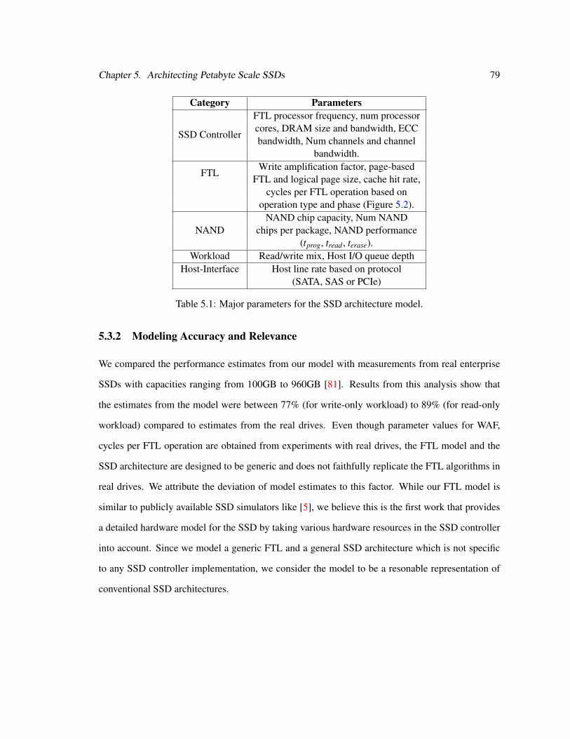
Chapter 5. Architecting Petabyte Scale SSDs 79
Category Parameters
SSD Controller
FTL processor frequency, num processorcores, DRAM size and bandwidth, ECCbandwidth, Num channels and channel
bandwidth.
FTLWrite amplification factor, page-based
FTL and logical page size, cache hit rate,cycles per FTL operation based on
operation type and phase (Figure 5.2).
NANDNAND chip capacity, Num NAND
chips per package, NAND performance(tprog, tread , terase).
Workload Read/write mix, Host I/O queue depthHost-Interface Host line rate based on protocol
(SATA, SAS or PCIe)
Table 5.1: Major parameters for the SSD architecture model.
5.3.2 Modeling Accuracy and Relevance
We compared the performance estimates from our model with measurements from real enterprise
SSDs with capacities ranging from 100GB to 960GB [81]. Results from this analysis show that
the estimates from the model were between 77% (for write-only workload) to 89% (for read-only
workload) compared to estimates from the real drives. Even though parameter values for WAF,
cycles per FTL operation are obtained from experiments with real drives, the FTL model and the
SSD architecture are designed to be generic and does not faithfully replicate the FTL algorithms in
real drives. We attribute the deviation of model estimates to this factor. While our FTL model is
similar to publicly available SSD simulators like [5], we believe this is the first work that provides
a detailed hardware model for the SSD by taking various hardware resources in the SSD controller
into account. Since we model a generic FTL and a general SSD architecture which is not specific
to any SSD controller implementation, we consider the model to be a resonable representation of
conventional SSD architectures.

Chapter 5. Architecting Petabyte Scale SSDs 80
8 16 32 64 128
SSD Capacity (in TB) - log scale
1
2
4
8
16
32
64
128
L2P T
able
Siz
e (
in G
B)
log s
cale
Logical page size4 KB
8 KB
16 KB
32 KB
Figure 5.3: L2P Table Size as a function of SSD Capacity and logical page size.Observations: (i) L2P table size grows with SSD capacity. (ii) DRAM cache capacity cannot scalewith the table size, so cache miss rate increases with table size and SSD capacity.
5.4 Scalability Challenges in Conventional SSD Architectures
5.4.1 Metrics, Workloads
We use SSD throughput measured in I/O Operations per Second (IOPS) as the performance metric
in this chapter. We also study the utilization of various SSD resources in the system to understand
resource bottlenecks. All performance results in this chapter are normalized to a baseline which
vary between studies and is defined at the beginning of the section describing that study. We use
the term SSD capacity to refer to the logical capacity of the drive to differentiate it from the SSD
physical capacity. In order to build versatile and robust storage systems that perform well under
a wide range of conditions, customers for enterprise SSDs benchmark the drives against random
I/O workloads using synthetic workload generators like Iometer [32]. Most SSD manufacturers
emphasize random workload performance of their drives since the key value-add for SSDs over
HDDs is their random workload performance [30,80]. Hence this study focuses on evaluating SSD
performance as a function of 100% random I/O workload using a synthetic workload generator
similar to IOMeter. We study SSD throughput as a function of read/write ratio in the workload
which varies from 0% to 100% at 25% increments and as a function of host I/O queue depth ranging

Chapter 5. Architecting Petabyte Scale SSDs 81
8 (Baseline)
16 32 64 128
SSD drive capacity (in TB)
60 %
70 %
80 %
90 %
100 %
Norm
aliz
ed t
hro
ughput Read-only
Figure 5.4: Impact of SSD capacity on random read throughput. Performance is normalized relativeto 8TB. Observation: As L2P cache hit rate reduces with SSD capacity, random read workloadperformance degrades.
from 1 to 256. All requests from the workload generator are assumed to be aligned to a 4K boundary
for this work.
5.4.2 L2P Table Size and Cache Capacity
As SSD capacity increases, the size of L2P table required to translate logical addresses to NAND
physical addresses increases significantly. In figure 5.3 we plot the size of the L2P table as a func-
tion of various logical page sizes for various SSD capacities. Given a SSD capacity (SSD logical
capacity) and the logical page size, the L2P table size can be calculated based on the following
equation:
L2P Table Size =ssd capacity
logical page size× log2(ssd physical capacity) (5.1)
All units are in Bytes. We notice that for a fixed logical page size, the size of the L2P table doubles as
capacity doubles. Similarly, for a fixed SSD capacity, the size of the L2P table halves as the logical
page size is doubled. In all cases, we can observe that as capacity increases, many gigabytes of
DRAM cache will be required to cache the entire L2P table. Considering that DRAM is expensive,
energy intensive and consumes significant SSD board space, caching even moderate portions of L2P
table is impractical. In Figure 5.4, we plot the performance impact of caching little or no portions

Chapter 5. Architecting Petabyte Scale SSDs 82
of the L2P table for a 4KB aligned 100% random read-only workload. We have implemented a
demand based caching algorithm, where table entries are paged-in from the NAND memory array
upon a cache miss. A cache hit or a miss is probablistically determined using a uniform random
variable that uses cache hit-rate a model parameter. We chose a read-only workload for this analysis
because these workloads trigger very little garbage collection (there are no host writes) and we can
clearly isolate the impact of L2P table management on SSD performance. The DRAM size is
maintained at 8GB while the logical page size is set to 4KB. Since the DRAM size is constant even
8 16 32 64 1280
25
50
75
100Write-only
8 16 32 64 128
75% writes
8 16 32 64 128
50% writes
8 16 32 64 128
25% writes
8 16 32 64 128SSD drive capacity (in TB)
SSD
contr
olle
r uti
lizati
on (
in %
)
Read-only
GC + Wear leveling
L2P Table Mgmt
Host I/O mgmt
Idle
Figure 5.5: SSD Controller Utilization for major operations as a function of drive capacity andworkload write intensity. Observations: (i) For all workloads, a majority of SSD controller re-sources are utilized for executing GC, WL and L2P page-in/page-out. (ii) As capacity scales, thefraction of resources spent on host I/O management reduces. (iii) Read-only workloads have a WAFclose to 1 and hence have little GC or wear leveling operations.
as the SSD capacity varies from 8TB to 128TB, the the DRAM cache hit rate for finding a valid L2P
map (i.e. the cache hit-rate) varies from 100% to 6.25%. As the capacity increases and the hit-rate
drops, the throughput of the drive drops steadily. Far from being able to increase performance with
SSD capacity, we notice that performance drops with capacity indicating that simple on-demand
caching algorithms proposed by Gupta et al. is not optimal in the context of petascale SSDs with
high cache miss rates [24]. In section 5.5.2 we propose a new table management scheme that works
better with petascale SSDs.
Chapter 5. Architecting Petabyte Scale SSDs 83
5.4.2.1 Drawbacks in existing solutions
Several existing studies have examined the impact of L2P table size on SSD performance and have
suggested mapping schemes to reduce the size of the L2P table [41, 44, 49, 50]. These studies
propose increasing the logical page size to reduce L2P table by mapping logical addresses at block
granularity or using a hybrid mapping approach where some sections of the table are mapped in
page granularity while the rest are mapped at block granularity. These approaches increase the
WAF which affect the endurance of NAND flash memory and degrades the performance of random
write workloads. In general, if we compare two SSDs (SSD4 and SSD8) that have a logical page
size of 4KB and 8KB, the WAF for SSD8 is twice the WAF for SSD4 for the same random 4K write
workload. Increase in WAF impacts NAND endurance since NAND memory array would have to
withstand more writes and erasures. Increasing the endurance requirement on the NAND memory
array increases the time to qualify, test and optimize the memory array, thereby increasing cost and
delaying time to market. In Figure 5.6, we show how WAF affects SSD performance due to high
GC overhead.
Based on these results, we make the following claim.
Claim 1: As SSDs approach the petascale capacity, the page-based L2P table mapping scheme
needs to be significantly modified to work with little or no DRAM cache while minimizing impact to
random workload performance.
5.4.3 SSD Controller Utilization
In Figure 5.6, we study the impact of SSD capacity on the performance of random write workloads.
We vary the write activity in the workload from 100% to 25% and plot the performance normalized
to the 8TB drive. For all the workloads, we assume a write amplification factor (WAF) of 5 and a
logical page size of 4KB. Our results indicate that, similar to the read-only random workload result
presented in Figure 5.4, random write workload performance reduces with capacity and is similar
in magnitude. In order to identify the reason behind the performance drop, we analyzed the FTL
processor utilization for various workloads in Figure 5.5 using our model. Since the FTL processor
is the only central resource responsible for the initiating, scheduling, dispatching and completing

Chapter 5. Architecting Petabyte Scale SSDs 84
various types of FTL tasks, the FTL processor utilization is also a reflection of SSD controller
utilization (i.e. utilization of other hardware units like NAND communication channels, DRAM,
ECC engine and NAND). For example, if the FTL processor executes host operations only, then
the DRAM, ECC, channels and NAND are expected to only process host data. Hence we use FTL
processor utilization metric as an alias for SSD controller utilization. We plot the SSD controller
utilization of each FTL task as a function of workload and SSD capacity. The results from Figure
5.5 along with results from Figure 5.6 and Figure 5.4 show why SSD performance decreases with
capacity.
From Figure 5.5, we can observe that for a given workload, the fraction of cycles spent by the
FTL processor on executing host I/O operations reduces as SSD capacity increases. As the FTL
processor spends more cycles executing non-host operations like garbage collection, wear leveling
and L2P table management, the host workload performance degrades. Results from Figure 5.6
and Figure 5.4 indicate a poor tradeoff for data center operators who are forced to choose between
slower but high capacity SSDs or faster but low capacity SSDs.
From Figure 5.5, we observe that for most workloads more than 50% of FTL processor cycles
is spent on non-host operations. For example, the percentage of controller cycles spent on non-host
operations varies from 74% (for 8TB) to 88% (for 128TB) for the write-only workload. If host
operations execute only 12% of the time in the FTL processor, we cannot expect a 128TB drive to
perform better than a 8TB drive. From Figure 5.5, we can observe that as SSD capacity increases,
the percentage of processor cycles spent executing L2P operations increases due to the reduction in
DRAM cache hit rate. For the 8TB drive capacity (irrespective of the workload), processor cycles
spent on L2P table operations is close to 0% since the entire L2P table is resident on the DRAM
cache. Since GC and wear leveling are a function of host write activity, as workload write intensity
drops, the fraction of cycles spent on these operations drop. Hence for a given capacity, results
from our model indicate that the performance of the drive increases as write intensity factor in the
workload decreases. For the read-only workload, we assume WAF=1 and hence there is no garbage
collection and wear leveling operations.
Based on the results presented in Figure 5.5, we make the following claim.
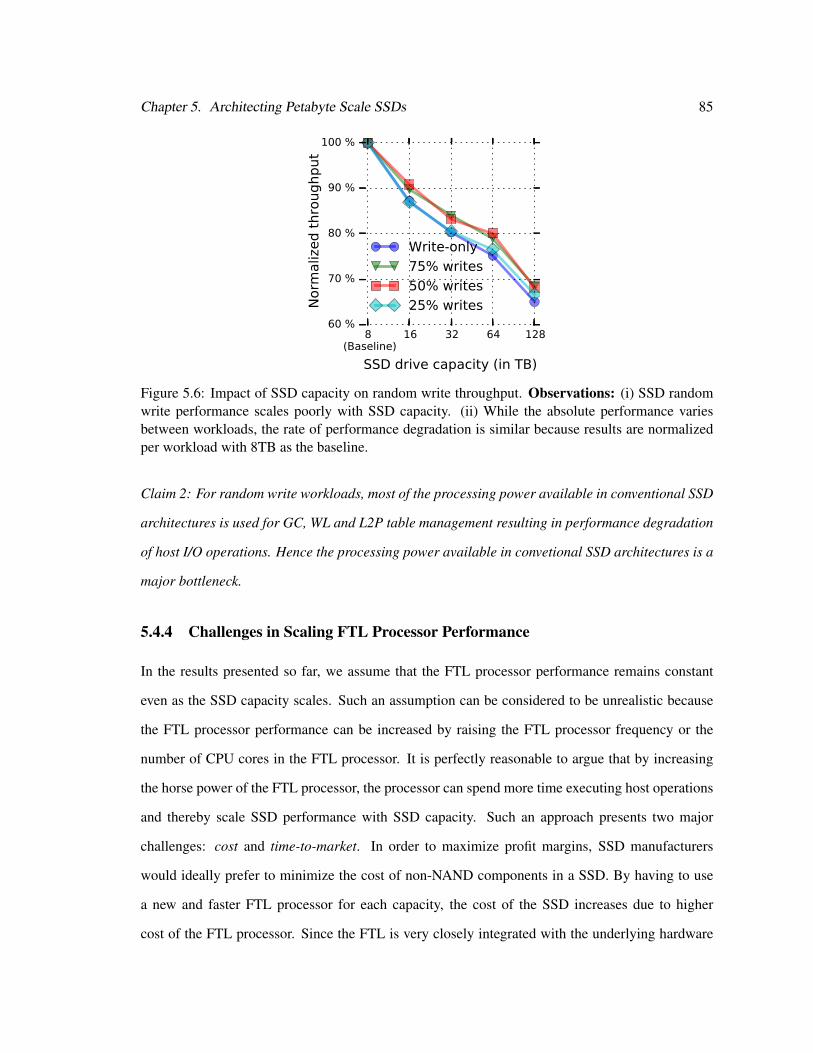
Chapter 5. Architecting Petabyte Scale SSDs 85
8 (Baseline)
16 32 64 128
SSD drive capacity (in TB)
60 %
70 %
80 %
90 %
100 %
Norm
aliz
ed t
hro
ughput
Write-only
75% writes
50% writes
25% writes
Figure 5.6: Impact of SSD capacity on random write throughput. Observations: (i) SSD randomwrite performance scales poorly with SSD capacity. (ii) While the absolute performance variesbetween workloads, the rate of performance degradation is similar because results are normalizedper workload with 8TB as the baseline.
Claim 2: For random write workloads, most of the processing power available in conventional SSD
architectures is used for GC, WL and L2P table management resulting in performance degradation
of host I/O operations. Hence the processing power available in convetional SSD architectures is a
major bottleneck.
5.4.4 Challenges in Scaling FTL Processor Performance
In the results presented so far, we assume that the FTL processor performance remains constant
even as the SSD capacity scales. Such an assumption can be considered to be unrealistic because
the FTL processor performance can be increased by raising the FTL processor frequency or the
number of CPU cores in the FTL processor. It is perfectly reasonable to argue that by increasing
the horse power of the FTL processor, the processor can spend more time executing host operations
and thereby scale SSD performance with SSD capacity. Such an approach presents two major
challenges: cost and time-to-market. In order to maximize profit margins, SSD manufacturers
would ideally prefer to minimize the cost of non-NAND components in a SSD. By having to use
a new and faster FTL processor for each capacity, the cost of the SSD increases due to higher
cost of the FTL processor. Since the FTL is very closely integrated with the underlying hardware

Chapter 5. Architecting Petabyte Scale SSDs 86
platform, having to rearchitect and optimize the entire architecture for each SSD capacity results
in longer time-to-market. In addition to presenting significant competitive challenges due longer
time-to-market, such a solution also increases SSD cost due to additional resources (like engineers,
verification, assembly, qualification, etc.) required to rearchitect the system. Ideally, SSD and
NAND memory manufacturers would prefer to build SSDs on top of a scalable SSD architecture
where SSD performance scales up as more NAND packages are added (i.e. SSD capacity scales)
without having to make significant changes to the FTL software. In this chapter, we present an SSD
architecture that can scale SSD performance with SSD capacity.
5.4.5 Host Interface Processor, ECC Engine and NAND
The performance of the host interface processor is based on the communication protocol of the
SSD (SSDs typically communicate via SAS, SATA or PCIe) and doesn’t create a bottleneck. If
and when the drive performance saturates the host interface, SSD manufacturers modify the host
interface processor to a protocol with higher performance. Similarly, the bandwidth of the ECC
engine is based to the total bandwidth of the NAND communication protocol. Since any data read
from or written to the NAND needs to pass through the ECC engine, as long as the ECC bandwidth
can match the total NAND channel bandwidth, the performance of the ECC engine does not limit
SSD performance. NAND flash chips form the other major portion of the SSD. The state-of-art
NAND flash chips are around 384Gb [29] and are expected to reach 1Tb (or 128GB) by the end of
this decade [36]. At 128GB per chip, a 128TB drive is expected to contain about 1000 NAND flash
chips. With so many NAND chips in the drive, we can infer that the performance of the drive is
determined by the utilization of chips by the SSD controller and not on the raw performance of the
chips themselves. Hence we conclude broadly conclude that the raw performance of NAND flash
chips does not limit SSD performance.
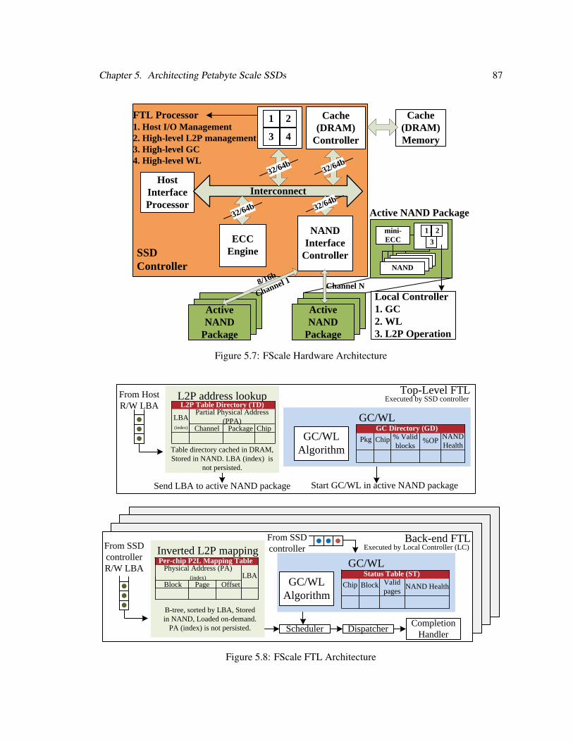
Chapter 5. Architecting Petabyte Scale SSDs 87
Active
NAND
Package
Active
NAND
Package
SSD
Controller
Host
Interface
Processor
Interconnect
ECC
Engine
Cache
(DRAM)
Controller
Cache
(DRAM)
Memory
NAND
Interface
Controller
32/64b32/64b
32/64b
32/64b
FTL Processor
1. Host I/O Management
2. High-level L2P management
3. High-level GC
4. High-level WL
1
4
2
3
Channel N
mini-
ECC
NAND
8
/16b
Channel 1
1 2
3̀
Local Controller
1. GC
2. WL
3. L2P Operation
Active NAND Package
Figure 5.7: FScale Hardware Architecture
From Host
R/W LBA
Send LBA to active NAND package Start GC/WL in active NAND package
Top-Level FTLL2P address lookupL2P Table Directory (TD)
LBA
(index) Channel Package Chip
Partial Physical Address
(PPA)
Table directory cached in DRAM,
Stored in NAND. LBA (index) is
not persisted.
GC/WL
GC/WL
Algorithm
GC Directory (GD)
Chip % Valid
blocks%OP
NAND
HealthPkg
Back-end FTLFrom SSD
controller
R/W LBA
Inverted L2P mapping
B-tree, sorted by LBA, Stored
in NAND, Loaded on-demand.
PA (index) is not persisted.
Per-chip P2L Mapping Table
Block Page Offset
Physical Address (PA)
(index) LBA
GC/WL
GC/WL
Algorithm
Status Table (ST)
Block Valid
pagesNAND HealthChip
From SSD
controller
Scheduler DispatcherCompletion
Handler
Executed by Local Controller (LC)
Executed by SSD controller
Figure 5.8: FScale FTL Architecture
Chapter 5. Architecting Petabyte Scale SSDs 88
5.5 FScale: A Scalable SSD Architecture
We propose to address the scalability challenges in conventional SSD architectures using FScale, a
distributed processor based SSD architecture targeted towards petabyte scale SSDs. Our design is
based on the observation that the conventional architectures use a centralized approach to SSD man-
agement and while such an approach was optimal until now, as SSD capacity scales, the bottlenecks
arising out of the centralized management prevent the system from scaling in the future.
Figure 5.7 and Figure 5.8 presents the FScale architecture. We now describe the architecture in
detail and explain how it resolves the two major bottleneck claims presented in Section 5.4.
5.5.1 FScale Hardware Architecture
Figure 5.7 presents the FScale hardware architecture. In the FScale architecture, the NAND pack-
ages are replaced by Active NAND packages which include a local controller, a mini-ECC engine
along with the NAND flash chips. Each active NAND package is essentially a mini-SSD with
enough hardware resources to manage the NAND flash chips within the package. The local con-
troller inside the active NAND package is a programmable, general purpose, lower power processor
that manages the NAND flash chips inside the package. The primary purpose of the local controller
is to execute major FTL tasks like garbage collection, wear leveling and L2P table management
while allowing the SSD controller to execute host I/O management tasks. Our design is essentially
a SSD within a SSD architecture, with the SSD controller managing the low-level SSDs within the
active NAND package and the local controller in the active NAND package is managed by the lo-
cal controller. Each active NAND package also contains a mini-ECC engine to handle bit errors
triggered during the read and write operation in the NAND flash. A mini-ECC engine is a low-
complexity ECC engine with a lower error detection and correction ability than the primary ECC
engine in the SSD controller. Studies have shown that the bit-error distribution due to endurance
and data retention in NAND flash memories has a long tail (i.e. only a very few percentage of
blocks suffer from high bit error rates) [12]. The ECC engine in the SSD controller is expected to
handle the long tails while the mini-ECC engine is expected to correct median bit-errors. Without

Chapter 5. Architecting Petabyte Scale SSDs 89
any ECC engine inside the active NAND package, all bit errors during NAND operations need to
be corrected by the ECC engine in the SSD controller resulting in unnecessary data traffic across
the NAND channels. By using a mini-ECC engine in the active NAND package, a majority of bit-
errors can be corrected within the active NAND package, thereby minimizing data traffic across the
NAND channels. During cases where the bit errors from the NAND is higher than the correction
capability of the mini-ECC engine, data can be moved to the ECC engine in the SSD controller
across the channel to correct the errors. To enable detection and error correction by ECC engines
of two different capabilities, we need to use a multi-phase data encoding format similar to [84] that
is compatible with both the ECC engines. The NAND and the local controller communicate via the
NAND communication protocol like ONFI or Toggle Mode and it is assumed that the communica-
tion protocol between the SSD controller and the active NAND package is assumed to be same as
the NAND protocol.
5.5.1.1 FScale Hardware Architecture Assumptions
We have built a FScale hardware architecture model by building an active NAND package model
and integrating it with our SSD model. For our analysis, we assume that our local controller is
similar to [7]. We assume that the bandwidth of mini-ECC engine is equal to the channel bandwidth
to minimize buffering during data transfers. Since SSD drive capacity is scaled by adding more
NAND packages, replacing NAND packages with active NAND packages enables us to scale the
processing power available in the SSD as capacity scales up. By adding more processing power
at the package-level instead of the chip-level, we prevent NAND cost from increasing so that SSD
manufacturers can use such packages only for the systems that need them.
5.5.2 FScale FTL Architecture
Figure 5.8 presents an outline of the FScale FTL architecture. This architecture has a two-level FTL
executing in the SSD. The SSD controller executes the top-level FTL while the local controller in
each active NAND package executes the second-level back-end FTL. We now explain both in detail.

Chapter 5. Architecting Petabyte Scale SSDs 90
5.5.2.1 Top-level FTL
The top-level FTL runs in the main SSD controller and is primarily responsible for managing the
active NAND packages and handling host commands. The L2P table is also segmented into two
levels with a top-level L2P Table Directory (TD) being managed by the SSD controller. While a
conventional L2P table maps a logical address to a complete physical address, the table directory
maps logical address to a Partial Physical Address (PPA). In the illustration shown in Figure 5.8,
each logical address maps to a chip address inside the NAND package. The rest of the address
mapping and execution of host operation happens at the back-end FTL. The TD is managed by the
SSD controller and cached in the DRAM. We observe that the total size of the L2P mapping table
(sum of TD size and second-level table) is still same as the conventional architecture but the size of
TD is significantly smaller than the size of the L2P table resulting in significant increase in cache
hit rate. We quantify this reduction and its impact on SSD performance in Section 5.6.
The top-level FTL executes a garbage collection and wear-leveling algorithm at the pack-
age/chip level using the GC/WL Directory table. It keeps track of valid block information and
NAND health at the package/chip level and instructs the active NAND package to execute GC op-
eration on a specific die. For example, the SSD controller does not need to know which NAND
block inside the chip has been garbage collected. This in contrast to the existing architecture where
the SSD controller is responsible for executing the complete operation and has to keep track of the
state of GC and WL of all dies and blocks in the system and manage the operations until they finish.
5.5.2.2 Back-end FTL
The back-end FTL assumes responsibility of the same tasks executed by the SSD controller with
one key difference: it is only responsible for managing the physical address space within it’s NAND
package and hence requires very little compute capability. The back-end FTL executes in the local
controller in the active NAND package and is responsible for scheduling and dispatching garbage
collection and wear-leveling operations. The back-end FTL executes address translation of logical
addresses to physical addresses. When the SSD controller sends a host request to the LC, the LC
reads the second-level inverted L2P table into it’s working memory and scans the table for the LBA.

Chapter 5. Architecting Petabyte Scale SSDs 91
Since the size of this entire table is in tens of megabytes, we load and scan partial regions of table
since the working memory size in the LC is very small (a few megabytes). We use a B-tree data
structure to store the Logical Block Address (LBA) in a sorted order. By using physical address
as the index to the inverted table, the size of the table is bound by the physical address space of
the NAND package/chip which is many orders of magnitude smaller than the logical space. Since
this size is fixed and the table is organized as B-tree data structure, the number of flash memory
accesses required to find a LBA inside the table is bound deterministically. In the illustration shown
in Figure 5.7, we have a per-chip mapping table which is loaded and scanned for the LBA. Once
a LBA match occurs, the physical address is automatically inferred and the data is read from this
physical address. During writes, the local controller determines the best block to write the new data
using its own wear leveling algorithm and writes data until the block is filled. When the block is
filled, a new block is chosen. The back-end FTL also keeps track of the valid pages and NAND
health information for all chips and blocks in the package for GC and WL using a GC/WL status
table. This is similar to the tables managed by conventional SSD architecture except that this table
is specific to the NAND blocks in the system. The back-end FTL implements it own scheduler,
dispatcher and completion handler to execute the host, GC/WL and L2P scan operations often
prioritizing host operations over the other operations to increase drive performance.
Having described the major properties of the FScale architecture, we now quantify how this
architecture handles the bottleneck claims presented in Section 5.4.
5.6 FScale Performance Results
5.6.1 L2P Table Size and Cache Capacity
In Figure 5.9, we compare the size of the L2P table used in the conventional architecture with that
of the L2P table directory used by the FScale architecture. Note that both these tables are cached
in SSD controller cache and any reduction in size of the table can increase cache hit rate since a
larger fraction of the table can be stored in the cache. We demonstrate the cache size reduction
for two logical page sizes (4KB and 32KB). Our results indicate that the L2P directory is 2.7X-4X
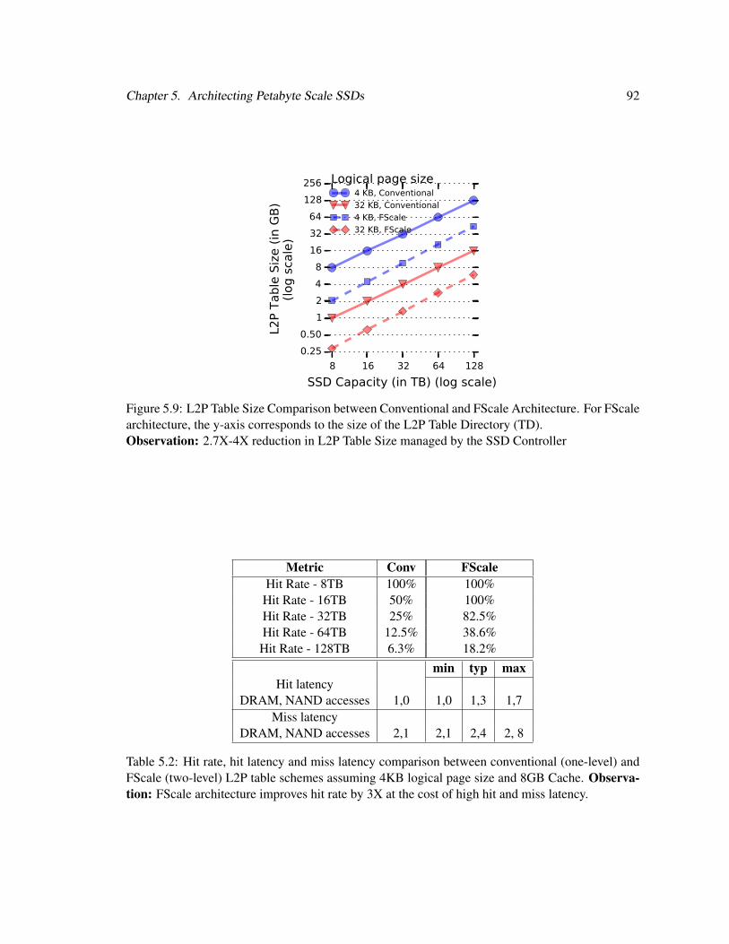
Chapter 5. Architecting Petabyte Scale SSDs 92
8 16 32 64 128
SSD Capacity (in TB) (log scale)
0.25
0.50
1
2
4
8
16
32
64
128
256
L2P T
able
Siz
e (
in G
B)
(log s
cale
)
Logical page size4 KB, Conventional
32 KB, Conventional
4 KB, FScale
32 KB, FScale
Figure 5.9: L2P Table Size Comparison between Conventional and FScale Architecture. For FScalearchitecture, the y-axis corresponds to the size of the L2P Table Directory (TD).Observation: 2.7X-4X reduction in L2P Table Size managed by the SSD Controller
Metric Conv FScaleHit Rate - 8TB 100% 100%Hit Rate - 16TB 50% 100%Hit Rate - 32TB 25% 82.5%Hit Rate - 64TB 12.5% 38.6%Hit Rate - 128TB 6.3% 18.2%
min typ maxHit latency
DRAM, NAND accesses 1,0 1,0 1,3 1,7Miss latency
DRAM, NAND accesses 2,1 2,1 2,4 2, 8
Table 5.2: Hit rate, hit latency and miss latency comparison between conventional (one-level) andFScale (two-level) L2P table schemes assuming 4KB logical page size and 8GB Cache. Observa-tion: FScale architecture improves hit rate by 3X at the cost of high hit and miss latency.

Chapter 5. Architecting Petabyte Scale SSDs 93
smaller than the conventional L2P table. In the table directory, width of each entry is cut by 2.7X-
4X because we truncate each entry to map only to a partial physical address (package/die offset)
instead of the entire physical address (package/die/block/page/offset). By re-architecting the L2P
table structure into a two-level table we can improve the cache hit rate. We have essentially applied
the multi-level page table architecture present in the Linux kernel to the L2P table and let the SSD
controller manage only the top-level directory [61].
Table 5.2 compares the hit rate, hit and miss latency impact of the proposed scheme against
the conventional scheme. We notice significant improvements in the hit rate while the hit and miss
latency of the proposed scheme is higher compared to the conventional scheme. In case of the
proposed scheme, there are 3 cases for hit and miss latency depending upon whether the second-
level table is already loaded in the local controller working memory or needs to be paged from
NAND for every read access.
5.6.2 FScale Performance Analysis
Figure 5.10 presents the performance impact of using the FScale architecture for various random
workloads. The performance of the conventional 8TB drive is used as the baseline for this analysis
with queue depth set to 32. First we notice that unlike conventional architecture, performance of
SSDs with FScale architecture scales with capacity for write intensive workloads (>= 50% writes).
Workloads with the highest write intensity (100% writes) have the highest performance improve-
ment. For example, the write-only workload performance of a 128TB drive is approximately 3 times
higher for the FScale architecture compared to the conventional architecture. Our results indicate
similar performance improvement for other write intensive workloads indicating that the FScale
architecture is successful in scaling SSD performance. We are able to scale performance because
of two major reasons: (i) by offloading garbage collection and wear-leveling to the local controller,
the FTL processor can spend more cycles on executing host operations and (ii) L2P cache hit rate
improves with the 2-level L2P table. Even though the hit and miss latency of the L2P table scheme
proposed in the FScale architecture is higher than the conventional architecture (as shown in Table
5.2), they do not impact write-intensive workloads since the write latency is one order of magnitude
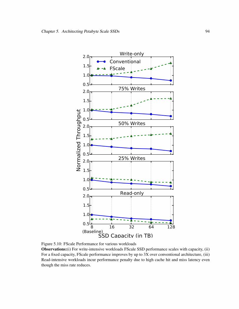
Chapter 5. Architecting Petabyte Scale SSDs 94
0.5
1.0
1.5
2.0Write-only
Conventional
FScale
0.5
1.0
1.5
2.075% Writes
0.5
1.0
1.5
2.0
Norm
aliz
ed T
hro
ughput
50% Writes
0.5
1.0
1.5
2.025% Writes
8 (Baseline)
16 32 64 1280.5
1.0
1.5
2.0Read-only
SSD Capacity (in TB)Figure 5.10: FScale Performance for various workloadsObservations:(i) For write-intensive workloads FScale SSD performance scales with capacity, (ii)For a fixed capacity, FScale performance improves by up to 3X over conventional architecture, (iii)Read-intensive workloads incur performance penalty due to high cache hit and miss latency eventhough the miss rate reduces.

Chapter 5. Architecting Petabyte Scale SSDs 95
higher for writes compared to reads. Increasing the cache hit rate in the SSD controller and reduc-
ing the number of scheduling and dispatching and completion operations is much more important
since they reduce the work done by the FTL processor and this translates to higher performance.
However, the higher hit and miss latencies (as shown in Table 5.2) impact the performance of
read-intensive (< 50% writes) workloads. As read intensity increases, the intensity of garbage col-
lection and wear leveling reduces which minimizes the use of the local controller. The performance
of the drive will then be bound by the host I/O processing latency and L2P table management
reducing the effectiveness of the FScale architecture. For the workload with 25% writes, while
the performance of FScale architecture is higher than the conventional architecture, performance
doesn’t scale with capacity. For the read-only workload, we observe that FScale performance is
lower than conventional architecture for all capacities and follows the decreasing trend indicating
that hit and miss latencies have a bigger impact than the hit rate.
Figure 5.11 plots the performance of a random read-only workload for various SSD capacities.
Given sufficient pending host operations, we wanted to determine if we could hide the cache hit
and miss latency penalty of FScale architecture and improve workload performance. We vary the
queue depth from 1 to 256 and the workload performance using the conventional architecture at a
queue depth of 1 serves as the baseline. Our results indicate that the performance of the drive with
conventional architecture saturate at higher queue depths while the performance of FScale SSDs
increases with queue depth. As queue depth increases (i.e. number of operations pending service
increases), FScale architecture can effectively hide the high cache hit and miss latency incurred by
requests by efficiently pipelining the requests. Hence the performance of the drive meets or exceeds
the conventional architecture.
5.6.3 Impact of Workload Queue Depth on FScale Performance
Our results indicate that the performance of the drive does not scale after a certain queue depth
(queue depth > 64) due to the compute limitations of the FTL processor in the conventional SSD
architecture. With FScale processor architecture, the performance of the SSD increases with queue
depth since the compute power in the SSD scales with SSD capacity. Results in Figure 5.10 for
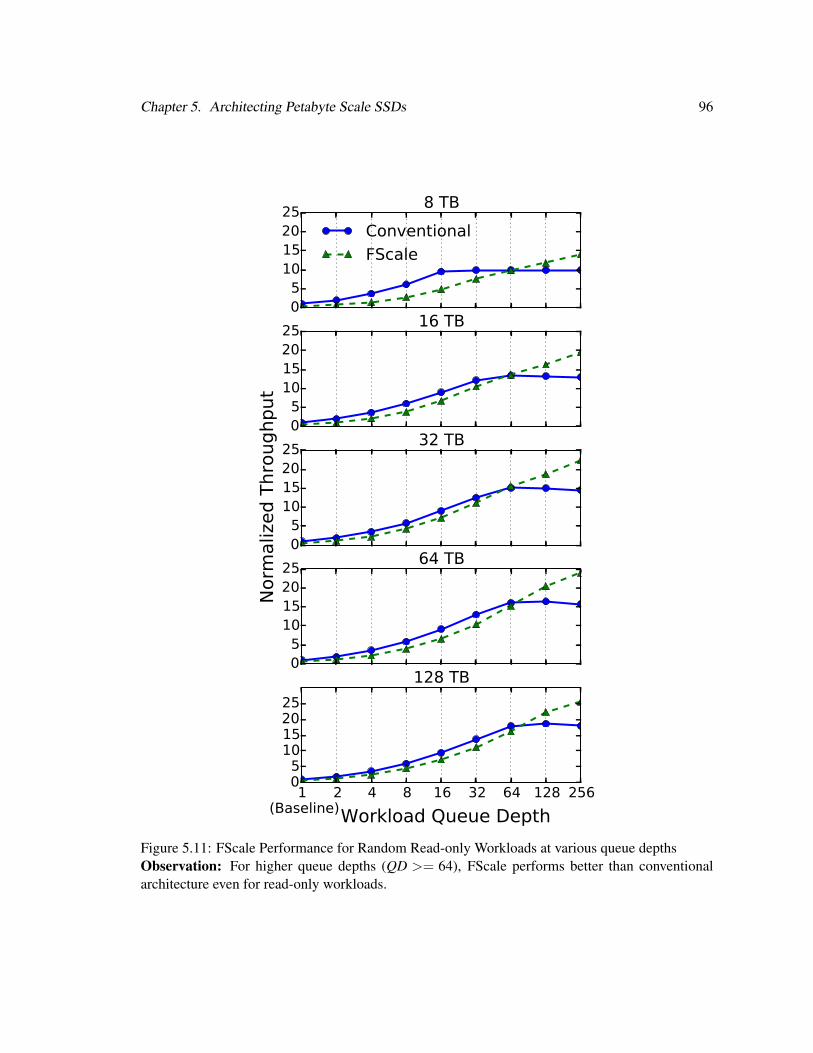
Chapter 5. Architecting Petabyte Scale SSDs 96
05
10152025
8 TB
Conventional
FScale
05
10152025
16 TB
05
10152025
Norm
aliz
ed T
hro
ughput
32 TB
05
10152025
64 TB
1 (Baseline)
2 4 8 16 32 64 128 25605
10152025
128 TB
Workload Queue Depth
Figure 5.11: FScale Performance for Random Read-only Workloads at various queue depthsObservation: For higher queue depths (QD >= 64), FScale performs better than conventionalarchitecture even for read-only workloads.

Chapter 5. Architecting Petabyte Scale SSDs 97
the read only workload were at a queue depth of 32 where FScale performance is still lower than
conventional SSD performance. However, we observe that at higher queue depths, the trends in
Figure 5.10 do not hold and the drives tend to have a steady performance irrespective of the SSD
capacity.
5.6.4 Other Advantages of FScale Architecture
FScale architecture helps in overcoming the cost and time-to-market challenges presented by the
conventional architecture. By scaling capacity by just adding more NAND packages, SSD man-
ufacturers can reduce the frequency at which they upgrade the SSD controller. This also reduces
time-to-market. The cost added by the local controller is negligible due to its minimal complexity.
While we haven’t evaluated the impact of FScale architecture on the power consumption of the
system in this work, features like low power processor and mini-ECC engine in the local controller
are directed towards minimizing the additional power dissipation.
5.7 Related Work
Most of the research on SSD architecture has been towards architecting megabyte and gigabyte
scale SSDs with little focus on SSD architecture scalability. Several algorithms have been proposed
to optimize SSD metrics like performance and reliability and quantifying the tradeoffs between
such metrics. We believe that this is the first work that focuses on the how such algorithms execute
on SSD hardware and quantify the computational bottlenecks involved in executing such algorithms
in the context of a typical SSD architecture.
Agrawal et al. explore the SSD architecture in detail and focus mainly on understanding the
tradeoffs involved in Flash Translation Layer (FTL) algorithms and its impact on SSD perfor-
mance [5]. Gupta et al. recommend a on-demand page-based address mapping policy for enter-
prise workloads [24] and provide insights into why high performance enterprise SSDs work better
with page-based mapping instead of a block-based or a hybrid mapping policy. One of the most
recent studies on SSD architecture for web-scale internet storage systems has been by Ouyang et
Chapter 5. Architecting Petabyte Scale SSDs 98
al [66, 67]. They describe a hardware/software co-designed storage system designed to exploit
memory array properties of flash and is highly optimized to work for specific types of workloads.
While such architectures work well for specific workloads, many customers build servers that are
deployed by a wide range of customers and are expected to work well for a broad range of work-
loads. For such environments, the FScale architecture is a better fit since it works well for a wide
range of workload categories without any workload specific optimizations. Tiwari et al. describe
Active Flash, an architecture optimized towards SSDs used in supercomputers that perform in-situ
scientific data analytics [95]. Their design optimizes the performance and energy efficiency of su-
percomputers by minimizing data movement between compute and storage nodes. For systems that
use SSD as a cache in front of a hard drives, Li et al. propose a new cache-optimized SSD archi-
tecture called Nitro [52]. Nitro primarily controls the workload traffic pattern arriving into the SSD
and hence is orthogonal to optimizations in FScale architecture.
5.8 Summary
In this chapter, we present a case for a new SSD architecture to ensure SSD performance scales with
capacity. Using a detailed architectural model, we quantify the bottlenecks in existing controller
architecture. We then propose FScale, a new scalable SSD architecture using a distributed processor
based solution. We evaluate the performance of FScale architecture and evaluate its scalability for
various workloads.
Chapter 6
Conclusions and Future Work
The invention of NAND flash memory in mid 1980s has spawned a new category of storage sys-
tems that is versatile with high performance, low power and robust compared to Hard Disk Drives
(HDDs). As flash memory scaled and cost per bit reduced, the range of applications using flash has
expanded significantly. With this expanded range and diverse application requirements, systems
architects are required to have a thorough understanding of the trade-offs involved in designing
application optimal storage systems. By building a set of analytical and architecture level models,
this dissertation presents original research contributions that is directed towards building energy
efficient, reliable and scalable NAND flash based storage systems.
In Chapter 2, this dissertation presents a detailed analytical model for flash memory consump-
tion. FlashPower has been validated with data from real world flash chips and can be used to
estimate the energy dissipated by NAND flash using various operations. This model has been
highly parameterized to study the impact of major parameters affecting NAND energy dissipation
and enable chip architects to design power optimal NAND flash chips. While this work primarily
focuses on 2D flash memory, the industry has started production of 3D flash based memory sys-
tems [29, 78, 96]. Hence, FlashPower model can be extended to study the energy dissipation of 3D
based NAND flash memory chips. In this work, we focused our attention on floating gate transistors
since a majority of 2D flash memory was built on top of floating gate transistors. As flash memory
scales to 3D, it has been noted that charge trap based transistors offer more advantages than floating
gate based transistors. By replacing the floating gate transistor model described in Chapter 2.3.5.1
99

Chapter 6. Conclusions and Future Work 100
with a charge trap based transistor model, FlashPower can still be leveraged to study the energy
dissipation of 3D NAND flash chips. FlashPower provides a modularized and parameterized model
that can be easily extended to study many NAND flash memory variants.
In Chapter 3, this dissertation presents a detailed analytical model to study NAND flash data
retention. Using FENCE, we show the effect of temperature and recovery periods, two important
system level parameters that affect NAND flash reliability, on data retention. We also show how
FENCE can be used to trade-off data retention to improve NAND flash endurance. Increasing
NAND flash endurance is critical for Solid State Disks (SSDs) used in data centers because of the
high write activity present in enterprise workloads. In Chapter 4, we use the reliability model to
improve the endurance of MLC based flash SSDs used in data centers. Since data stored in en-
terprise storage systems is backed up periodically, we can trade-off data retention to increase flash
endurance and enable low cost and high endurance storage systems for data centers. In this chapter,
we also propose a methodology to use existing hard-drive based workload traces and convert them
into equivalent SSD workload traces for system evaluation. This research can be extended in sev-
eral ways. With the advent of 3D NAND and the differences in failure mechanisms, it is important
to identify the predominant failure modes in 3D memory and modify FENCE to understand the
trade-offs involved in new failure modes. While we expect data retention and endurance to remain
primary concerns, additional failure modes like read or program disturbs can impact memory relia-
bility. It is also important to understand the impact of new failure modes on system level reliability
and re-architect SSD level firmware and hardware architectures to design highly reliable storage
systems.
In Chapter 5, this dissertation focuses on SSD architecture and the impediments faced by con-
ventional architectures in increasing performance of high capacity SSDs. Using data from drive-
level measurements and a detailed architecture-level model, we show that conventional architec-
tures scale poorly due to limited computational power in conventional architecture. As the number
of NAND flash chips approach several hundreds (perhaps even thousands), we show that a cen-
tralized controller architecture prevents maximizing NAND utilization, resulting in reduced system
performance. We propose FScale, a new distributed processor based SSD architecture to overcome

Chapter 6. Conclusions and Future Work 101
this limitation and maximize NAND utilization. By integrating a small, energy efficient and low
cost controller to a NAND package and managing NAND local to the package, we can scale the
system efficiently and increase performance with SSD capacity. An alternative approach to increase
SSD scalability is by increasing computational power in current architectures by adding more cores
to the central processor. Implementing this approach requires detailed analysis to determine the
core count required to manage NAND chips for an optimal design. SSD architects have to trade-off
the design complexity of using a many-core processor in petascale SSDs with several distributed
processors based on factors like time-to-market, power dissipation and firmware and hardware ar-
chitecture complexity. FScale architecture can be extended to include one low powered, low com-
plexity micro-controller per NAND chip instead of a controller per NAND package (a group of
NAND chips). Such a system can provide better scalability because the computational power can
be extended as a function of number of chips and prevent us from over designing the central pro-
cessor. However, this approach increases the cost of flash chips since each chip now includes a
micro-controller and can impact other parameters like chip yield and increase in design complexity.
Architecting scalable SSDs is still an open problem and there can be several approaches to address
this issue. In this dissertation, I present one approach to address this problem and quantify the
advantages and disadvantages of the proposed architecture.
6.1 Emerging Non Volatile Memories and Evolution of Memory Hier-
archy
The advent of new non volatile memory technologies like Phase Change Memory (PCM) and Spin-
Transfer Torque (STT) RAM is expected to add a new dimension in designing memory and storage
systems. NAND flash memory is not left expected to be left behind and continues to scale into 3D.
As these new memory technologies mature, the 4 level conventional memory hierarchy (consisting
of registers, caches, main memory and storage) will continue to evolve and expand into many
more levels. For example, the performance, power and cost characteristics of PCM makes it as
an good candidate between the main memory and storage memory [1, 2], while the characteristics

Chapter 6. Conclusions and Future Work 102
of Spin-Transfer Torque memory makes it a good candidate to be used as a DRAM replacement or
complement [88]. Such an evolution will require systems architects to work very closely with device
physicists and memory designers to design optimal and efficient memory and storage systems. In
this dissertation, I have applied insights learnt from the device and circuit level to optimize NAND
flash memory energy dissipation and reliability while addressing SSD architecture challenges that
arise with the scaling of NAND flash memory.

Bibliography
[1] 3D Xpoint™. http://www.intel.com/content/www/us/en/
architecture-and-technology/3d-xpoint-unveiled-video.html.
[2] 3D Xpoint™. http://www.micron.com/about/innovations/3d-xpoint-technology.
[3] J. Abella, X. Vera, and A. Gonzalez. Penelope: The NBTI-Aware Processor. In Proceedings
of the 40th IEEE/ACM International Symposium on Microarchitecture, 2007.
[4] Advanced Microcontroller Bus Architecture (AMBA). http://infocenter.arm.com/
help/index.jsp?topic=/com.arm.doc.ddi0438d/BABDEDDA.html.
[5] N. Agrawal and et al. Design Tradeoffs for SSD Performance. In Proceedings the USENIX
Technical Conference (USENIX), 2008.
[6] Amazon.com. http://www.amazon.com.
[7] ARM Cortex M Series. http://www.arm.com/products/processors/cortex-m/
index.php.
[8] Andrea C. Arpaci-Dusseau, Remzi H. Arpaci-Dusseau, and Vijayan Prabhakaran. Removing
the costs of indirection in flash-based ssds with nameless writes. In Proceedings of the 2nd
USENIX conference on Hot topics in storage and file systems, HotStorage’10, pages 1–1,
Berkeley, CA, USA, 2010. USENIX Association.
[9] Andrew Birrell, Michael Isard, Chuck Thacker, and Ted Wobber. A design for high-
performance flash disks. SIGOPS Oper. Syst. Rev., 41(2):88–93, April 2007.
103

Bibliography 104
[10] S. Boboila and P. Desnoyers. Write Endurance in Flash Drives: Measurements and Analysis.
In Proceedings of the USENIX Conference on File and Storage Technologies (FAST), 2010.
[11] J.E. Brewer and M. Gill, editors. Nonvolatile Memory Technologies with Emphasis on Flash.
IEEE Press, 2008.
[12] Yu Cai, Onur Mutlu, Erich F Haratsch, and Ken Mai. Program interference in mlc nand flash
memory: Characterization, modeling, and mitigation. In Computer Design (ICCD), 2013
IEEE 31st International Conference on, pages 123–130. IEEE, 2013.
[13] Feng Chen, Tian Luo, and Xiaodong Zhang. Caftl: a content-aware flash translation layer
enhancing the lifespan of flash memory based solid state drives. In Proceedings of the 9th
USENIX conference on File and stroage technologies, FAST’11, pages 6–6, Berkeley, CA,
USA, 2011. USENIX Association.
[14] Jim Cooke. Introduction to Flash Memory (T1A), 2008. http://download.micron.com/
pdf/presentations/events/FMS08_Intro_to_Flash_Memory_Jim_Cooke.pdf.
[15] C. Delimitrou, S. Sankar, K. Vaid, and C. Kozyrakis. Storage i/o generation and replay for
datacenter applications. In Performance Analysis of Systems and Software (ISPASS), 2011
IEEE International Symposium on, pages 123 –124, april 2011.
[16] P. Desnoyers. Empirical Evaluation of NAND Flash Memory Performance. In Proceedings
of the Workshop on Hot Topics in Storage and File Systems (HotStorage), October 2009.
[17] D. J. DiMaria and E. Cartier. Mechanism for stress induced leakage currents in thin silicon
dioxide films. Journal of Applied Physics, 78(6):3883 –3894, sep 1995.
[18] Xiangyu Dong, Norman P. Jouppi, and Yuan Xie. PCRAMsim: system-level performance,
energy, and area modeling for Phase-Change RAM. In Proceedings of the 2009 International
Conference on Computer-Aided Design, pages 269–275, 2009.
[19] Flash-Transformed Data Center. http://www.sandisk.com/assets/docs/
the-flash-transformed-data-center-whitepaper.pdf.

Bibliography 105
[20] Reducing Data Center Power Consumption Through Efficient Storage, 2009.
http://www.gtsi.com/eblast/corporate/cn/06_2010/PDFs/NetApp%20Reducing%
20Datacenter%20Power%20Consumption.pdf.
[21] The Diverse and Exploding Digital Universe: An Updated Forecast of World-
wide Information Growth Through 2011, 2008. http://www.emc.com/collateral/
analyst-reports/diverse-exploding-digital-universe.pdf.
[22] Growth in SD Card Capacity . http://goo.gl/QcXK1R.
[23] L. Grupp and et al. Characterizing flash memory: Anomalies, observations, and applications.
In Microarchitecture, 2009. MICRO-42. 2009 42nd IEEE/ACM International Symposium on,
2009.
[24] A. Gupta, Y. Kim, and B. Urgaonkar. DFTL: a flash translation layer employing demand-
based selective caching of page-level address mappings. In ASPLOS ’09: Proceeding of
the 14th international conference on Architectural support for programming languages and
operating systems, pages 229–240, 2009.
[25] Aayush Gupta, Raghav Pisolkar, Bhuvan Urgaonkar, and Anand Sivasubramaniam. Lever-
aging value locality in optimizing nand flash-based ssds. In Proceedings of the 9th USENIX
conference on File and stroage technologies, FAST’11, pages 7–7, Berkeley, CA, USA,
2011. USENIX Association.
[26] Hairong Sun, Pete Grayson, and Bob Wood. Quantifying Reliability of Solid-State Storage
from Multiple Aspects. In 7th IEEE International Workshop on Storage Network Architec-
ture and Parallel I/O, 2011. http://storageconference.org/2011/Papers/SNAPI/1.
Sun.pdf.
[27] HyperTransport. http://www.amd.com/en-us/innovations/
software-technologies/hypertransport.

Bibliography 106
[28] Intel CoFluent Studio. http://www.intel.com/content/www/us/en/cofluent/
intel-cofluent-studio.html.
[29] Intel-Micron 3D NAND. http://newsroom.intel.com/community/intel_newsroom/
blog/2015/03/26/micron-and-intel-unveil-new-3d-nand-flash-memory.
[30] Inte SSD Product Comaprison. http://www.intel.com/content/www/us/en/
solid-state-drives/solid-state-drives-ssd.html.
[31] Intel X25-M and X18-M Mainstream SATA Solid-State Drives. http://ark.intel.com/
products/series/78570/Intel-SSD-X25-M-Series.
[32] Iometer Project. http://www.iometer.org.
[33] K. Ishida and et al. A 1.8V 30nJ adaptive program-voltage (20V) generator for 3D-integrated
NAND flash SSD. In Solid-State Circuits Conference - Digest of Technical Papers, pages
238–239,239a, 2009.
[34] Process Integration and Device Structures, ITRS 2009 Edition. http://www.itrs.net/
links/2009ITRS/2009Chapters_2009Tables/2009Tables_FOCUS_C_ITRS.xls.
[35] Process Integration and Device Structures, ITRS 2011 Edition. http://www.itrs.net/
Links/2011ITRS/2011Tables/PIDS_2011Tables.xlsx.
[36] Process Integration and Device Structures, ITRS 2013 Edition. http://www.itrs.
net/ITRS%201999-2014%20Mtgs,%20Presentations%20&%20Links/2013ITRS/
2013TableSummaries/2013ORTC_SummaryTable.pdf.
[37] J. de Blauwe, J. van Heudt, D. Wellekens, G. Groeseneken, and H.E. Maes. SILC-related
effects in flash E2PROM’s-Part I: A quantitative model for steady-state SILC. Electron
Devices, IEEE Transactions on, 45(8):1745 –1750, August 1998.
[38] J. de Blauwe, J. van Heudt, D. Wellekens, G. Groeseneken, and H.E. Maes. SILC-related
effects in flash E2PROM’s-Part II: Prediction of steady-state SILC-related disturb character-
istics. Electron Devices, IEEE Transactions on, 45(8):1751 –1760, August 1998.

Bibliography 107
[39] JEDEC - Solid-State Drive (SSD) Requirements and Endurance Test Method. http://www.
jedec.org/sites/default/files/docs/JESD218.pdf.
[40] JEDEC - Failure Mechanisms and Models for Semiconductor Devices. http://www.jedec.
org/sites/default/files/docs/JEP122F.pdf.
[41] Dawoon Jung, Jeong-UK Kang, Heeseung Jo, Jin-Soo Kim, and Joonwon Lee. Superblock
ftl: A superblock-based flash translation layer with a hybrid address translation scheme.
ACM Trans. Embed. Comput. Syst., 9(4):40:1–40:41, April 2010.
[42] M. Jung, E.H. Wilson, D. Donofrio, J. Shalf, and M.T. Kandemir. NANDFlashSim: In-
trinsic latency variation aware NAND flash memory system modeling and simulation at mi-
croarchitecture level. In Mass Storage Systems and Technologies (MSST), 2012 IEEE 28th
Symposium on, 2012.
[43] Asim Kadav, Mahesh Balakrishnan, Vijayan Prabhakaran, and Dahlia Malkhi. Differential
raid: rethinking raid for ssd reliability. SIGOPS Oper. Syst. Rev., 44:55–59, March 2010.
[44] Jesung Kim, Jong Min Kim, S.H. Noh, Sang Lyul Min, and Yookun Cho. A space-efficient
flash translation layer for compactflash systems. Consumer Electronics, IEEE Transactions
on, 48(2):366–375, May 2002.
[45] J.K. Kim and et al. A PRAM and NAND flash hybrid architecture for high-performance
embedded storage subsystems. In EMSOFT ’08: Proceedings of the 8th ACM international
conference on Embedded software, pages 31–40, New York, NY, USA, 2008. ACM.
[46] R. Kumar, D.M. Tullsen, and N.P. Jouppi. Core Architecture Optimization of Heterogeneous
Chip Multiprocessors. In Proceedings of the International Conference on Parallel Architec-
tures and Compilation Techniques (PACT), September 2006.
[47] L. Larcher, S. Bertulu, and P. Pavan. SILC effects on E2PROM memory cell reliability.
Device and Materials Reliability, IEEE Transactions on, 2(1):13 –18, mar 2002.

Bibliography 108
[48] J. Lee and et al. A 90-nm CMOS 1.8-V 2-Gb NAND flash memory for mass storage appli-
cations. Solid-State Circuits, IEEE Journal of, 38(11):1934–1942, 2003.
[49] S. Lee, D. Park, T. Chung, D. Lee, S. Park, and H. Song. A Log Buffer based Flash Trans-
lation Layer Using Fully Associative Sector Translation. IEEE Transactions on Embedded
Computing Systems, 6(3), July 2007.
[50] S. Lee, D. Shin, Y. Kim, and J. Kim. LAST: Locality-Aware Sector Translation for NAND
Flash Memory-Based Storage Systems. In Proceedings of the International Workshop
on Storage and I/O Virtualization, Performance, Energy, Evaluation, and Dependability
(SPEED), February 2008.
[51] M. Lenzlinger and E.H. Snow. Fowler-Nordheim tunneling into thermally grown SiO2. Elec-
tron Devices, IEEE Transactions on, 15(9):686–686, 1968.
[52] Cheng Li, Philip Shilane, Fred Douglis, Hyong Shim, Stephen Smaldone, and Grant Wallace.
Nitro: a capacity-optimized ssd cache for primary storage. In Proceedings of the USENIX
Annual Technical Conferences (USENIX), June 2014.
[53] Xiang Luojie and B.M. Kurkoski. An improved analytic expression for write amplification
in nand flash. In Computing, Networking and Communications (ICNC), 2012 International
Conference on, pages 497–501, Jan 2012.
[54] Marvell SSD Controller. http://www.marvell.com/storage/assets/Marvell_
88SS9187-001.pdf.
[55] N. Mielke and et al. Recovery effects in the distributed cycling of flash memories. In Re-
liability Physics Symposium Proceedings, 2006. 44th Annual., IEEE International, pages
29–35, March 2006.
[56] N. Mielke, T. Marquart, Ning Wu, J. Kessenich, H. Belgal, E. Schares, F. Trivedi, E. Good-
ness, and L.R. Nevill. Bit error rate in nand flash memories. In Reliability Physics Sympo-
sium, 2008. IRPS 2008. IEEE International, pages 9 –19, May 2008.

Bibliography 109
[57] Moazzami, R. and Chenming Hu. Stress-induced current in thin silicon dioxide films. In
Electron Devices, IEEE Transactions on, pages 139 –142, December 1992.
[58] Vidyabhushan Mohan, Trevor Bunker, Laura Grupp, Sudhanva Gurumurthi, Mircea R. Stan,
and Steven Swanson. Modeling Power Consumption of NAND Flash Memories Using Flash-
Power. Computer-Aided Design of Integrated Circuits and Systems, IEEE Transactions on,
32(7):1031–1044, July 2013.
[59] Vidyabhushan Mohan, Sudhanva Gurumurthi, and Mircea R. Stan. FlashPower: A Detailed
Power Model for NAND flash memory. In Design, Automation Test in Europe Conference
Exhibition (DATE), 2010, pages 502 –507, march 2010.
[60] Vidyabhushan Mohan, Taniya Siddiqua, Sudhanva Gurumurthi, and Mircea R. Stan. How I
Learned to Stop Worrying and Love Flash Endurance. In Proceedings of the 2nd USENIX
conference on Hot topics in storage and file systems, HotStorage’10, Berkeley, CA, USA,
2010. USENIX Association.
[61] Linux Page Table Management. https://www.kernel.org/doc/gorman/html/
understand/understand006.html.
[62] Typical Data Retention for Nonvolatile Memory. http://www.freescale.com/files/
microcontrollers/doc/eng_bulletin/EB618.pdf.
[63] Typical Data Retention for Nonvolatile Memory. http://www.spansion.com/Support/
AppNotes/EnduranceRetention_AN.pdf.
[64] NVSim. http://www.rioshering.com/nvsimwiki/index.php?title=Main_Page.
[65] OCZ Deneva - eMLC based SSD. http://www.oczenterprise.com/downloads/
solutions/ocz-deneva2-c-mlc-2.5in_Product_Brief.pdf.
[66] Jian Ouyang, Shiding Lin, Zhenyu Hou, Peng Wang, Yong Wang, and Guangyu Sun. Active
ssd design for energy-efficiency improvement of web-scale data analysis. In Proceedings
Bibliography 110
of the 2013 International Symposium on Low Power Electronics and Design, ISLPED ’13,
pages 286–291, Piscataway, NJ, USA, 2013. IEEE Press.
[67] Jian Ouyang, Shiding Lin, Song Jiang, Zhenyu Hou, Yong Wang, and Yuanzheng Wang.
Sdf: Software-defined flash for web-scale internet storage systems. In Proceedings of the
19th International Conference on Architectural Support for Programming Languages and
Operating Systems, ASPLOS ’14, pages 471–484, New York, NY, USA, 2014. ACM.
[68] Yangyang Pan, Guiqiang Dong, Qi Wu, and Tong Zhang. Quasi-Nonvolatile SSD: Trading
Flash Memory Nonvolatility to Improve Storage System Performance for Enterprise Ap-
plications. In 2012 IEEE 17th International Symposium on High Performance Computer
Architecture (HPCA), feb. 2012.
[69] E. Pinheiro, W-D. Weber, and L.A. Barroso. Failure Trends in a Large Disk Drive Popula-
tion. In Proceedings of the USENIX Conference on File and Storage Technonologies (FAST),
February 2007.
[70] PMC SSD Controller. http://pmcs.com/products/storage/flashtec_nvme_
controllers/pm8604/.
[71] Qi Wu and Guiqiang Dong and Tong Zhang. Exploiting Heat-Accelerated Flash Memory
Wear-Out Recovery to Enable Self-Healing SSDs. In Proceedings of the 3rd USENIX con-
ference on Hot topics in storage and file systems, HotStorage’11, Berkeley, CA, USA, 2011.
USENIX Association.
[72] Quality Comparison of SLC, MLC and eMLC, 2011. http://www.flashmemorysummit.
com/English/Collaterals/Proceedings/2011/20110809_F2C_Wu.pdf.
[73] Quick Path Interconnect. http://www.intel.com/content/www/us/en/io/
quickpath-technology/quick-path-interconnect-introduction-paper.html.

Bibliography 111
[74] Ren-Shuo Liu and Chia-Lin Yang, and Wei Wu. Optimizing NAND Flash-Based SSDs via
Retention Relaxation. In Proceedings of the 8th USENIX conference on File and storage
technologies, FAST’12, 2012.
[75] S. Kavalanekar and et al. Characterization of storage workload traces from production Win-
dows servers. In Proceedings of the IEEE International Symposium on Workload Character-
ization (IISWC), pages 119–128, October 2008.
[76] Koji Sakui. Intel Corporation/Tohoku University, May 2009. Private Correspondence.
[77] Samsung corporation. K9XXG08XXM flash memory specification. K9XXG08XXM
Datasheet.
[78] Samsung V-NAND. http://www.samsung.com/global/business/semiconductor/
product/vnand/overview.
[79] SandForce SSD Controller. http://www.seagate.com/products/
solid-state-flash-storage/flash-controllers/enterprise-flash-controller.
[80] SanDisk Enterprise Solutions. http://www.sandisk.com/enterprise.
[81] SanDisk Enterprise SSDs. http://www.sandisk.com/enterprise/sata-ssd/.
[82] S. Sankar, M. Shaw, and K. Vaid. Impact of temperature on hard disk drive reliability in large
datacenters. In Dependable Systems Networks (DSN), 2011 IEEE/IFIP 41st International
Conference on, pages 530 –537, june 2011.
[83] H. Schmidt and et al. Tid and see tests of an advanced 8 gbit nand-flash memory. In Radiation
Effects Data Workshop, 2008 IEEE, pages 38 –41, 2008.
[84] E. Sharon, I. Alrod, and S. Litsyn. Multi-phase ecc encoding using algebraic codes, Febru-
ary 4 2014. US Patent 8,645,789.
[85] J. Shin, V. Zyuban, P. Bose, and T. Pinkston. A Proactive Wearout Recovery Approach of
Exploiting Microarchitectural Redundancy to Extend Cache SRAM Lifetime. In Proceed-
Bibliography 112
ings of the International Symposium on Computer Architecture (ISCA), pages 353–362, June
2008.
[86] Clinton W. Smullen, IV, Anurag Nigam, Sudhanva Gurumurthi, and Mircea R. Stan. The
STeTSiMS STT-RAM simulation and modeling system. In Proceedings of the International
Conference on Computer-Aided Design, pages 318–325. IEEE Press, 2011.
[87] Smullen, Clint and Mohan, Vidyabhushan and Nigam, Anurag. and Gurumurthi, Sudhanva
and Stan, Mircea R. Relaxing non-volatility for fast and energy-efficient STT-RAM caches.
In High Performance Computer Architecture (HPCA), 2011 IEEE 17th International Sym-
posium on, pages 50–61. IEEE, 2011.
[88] Clinton Wills Smullen IV. Designing Giga-scale Memory Systems with STT-RAM. PhD
thesis, University of Virginia, 2011.
[89] Gokul Soundararajan, Vijayan Prabhakaran, Mahesh Balakrishnan, and Ted Wobber. Extend-
ing ssd lifetimes with disk-based write caches. In Proceedings of the 8th USENIX conference
on File and storage technologies, FAST’10, pages 8–8, Berkeley, CA, USA, 2010. USENIX
Association.
[90] K.D. Suh and et al. A 3.3V 32 Mb NAND flash memory with incremental step pulse pro-
gramming scheme. Solid-State Circuits, IEEE Journal of, 30(11):1149–1156, 1995.
[91] K. Takeuchi, T. Tanaka, and T. Tanzawa. A multipage cell architecture for high-speed
programming multilevel NAND flash memories. Solid-State Circuits, IEEE Journal of,
33(8):1228 –1238, 1998.
[92] T. Tanaka and et al. A quick intelligent page-programming architecture and a shielded bitline
sensing method for 3V-only nand flash memory. Solid-State Circuits, IEEE Journal of,
29(11):1366–1373, 1994.
[93] Application Report: MSP430 Flash Memory Characteristics.
http://focus.ti.com/lit/an/slaa334a/slaa334a.pdf.
Bibliography 113
[94] A. Tiwari and J. Torrellas. Facelift: Hiding and Slowing Down Aging in Multicores. In Pro-
ceedings of the International Symposium on Microarchitecture (MICRO), November 2008.
[95] Devesh Tiwari, Simona Boboila, Sudharshan S Vazhkudai, Youngjae Kim, Xiaosong Ma, Pe-
ter Desnoyers, and Yan Solihin. Active flash: towards energy-efficient, in-situ data analytics
on extreme-scale machines. In FAST, pages 119–132, 2013.
[96] Toshiba-Sandisk 3D NAND. http://goo.gl/vQqwsL.
[97] Vidyabhushan Mohan, Sriram Sankar and Sudhanva Gurumurthi. reFresh SSDs: Enabling
High Endurance, Low Cost Flash in Datacenters. Technical Report CS-2012-05, Department
of Computer Science, University of Virginia, Charlottesville, 2012.
[98] Kashi Venkatesh Vishwanath and Nachiappan Nagappan. Characterizing cloud computing
hardware reliability. In Proceedings of the 1st ACM symposium on Cloud computing, SoCC
’10, pages 193–204, New York, NY, USA, 2010. ACM.
[99] David Tawei Wang. Modern DRAM Memory Systems: Performance analysis and a high
performance, power-constrained DRAM scheduling algorithm. PhD thesis, University of
Maryland, College Park, 2005.
[100] S.J.E. Wilton and N.P. Jouppi. Cacti: an enhanced cache access and cycle time model. Solid-
State Circuits, IEEE Journal of, 31(5):677–688, 1996.
[101] Cong Xu, Xiangyu Dong, N.P. Jouppi, and Yuan Xie. Design implications of memristor-
based rram cross-point structures. In Design, Automation Test in Europe Conference Exhibi-
tion (DATE), 2011, pages 1 –6, 2011.
[102] E. Yaakobi, Jing Ma, L. Grupp, P.H. Siegel, S. Swanson, and J.K. Wolf. Error characteri-
zation and coding schemes for flash memories. In GLOBECOM Workshops (GC Wkshps),
2010 IEEE, pages 1856 –1860, 2010.

Bibliography 114
[103] R. Yamada and et al. A novel analysis method of threshold voltage shift due to detrap in a
multi-level flash memory. In Symposium on VLSI Technology, Digest of Technical Papers,
2001.
[104] H. Yang and et al. Reliability issues and models of sub-90nm NAND flash memory cells. In
International Conference on Solid-State and Integrated Circuit Technology, 2006.
[105] Qing Yang and Jin Ren. I-cash: Intelligently coupled array of ssd and hdd. In High Perfor-
mance Computer Architecture (HPCA), 2011 IEEE 17th International Symposium on, pages
278 –289, feb. 2011.


![10 Traits Equanimous Leader_concept 1[2]](https://img.pdfslide.us/doc/110x75/55c3c340bb61ebd7048b4837/10-traits-equanimous-leaderconcept-12.jpg)