Embed Size (px)
Citation preview
Towards a Better Mechanistic Understanding of theDegradation Processes of Perovskite Solar Cells
Carlos Biaou
Electrical Engineering and Computer SciencesUniversity of California at Berkeley
Technical Report No. UCB/EECS-2018-3http://www2.eecs.berkeley.edu/Pubs/TechRpts/2018/EECS-2018-3.html
January 23, 2018

Copyright © 2018, by the author(s).All rights reserved.
Permission to make digital or hard copies of all or part of this work forpersonal or classroom use is granted without fee provided that copies arenot made or distributed for profit or commercial advantage and that copiesbear this notice and the full citation on the first page. To copy otherwise, torepublish, to post on servers or to redistribute to lists, requires prior specificpermission.
Acknowledgement
This work was made possible by a National Science Foundation GraduateResearch Fellowship, a Chancellor’s Fellowship, and a Jack Kent CookeFoundation Graduate Scholarship. Prof. Ana Arias’ gracefulness andgenerosity is applauded for sharing her lab tools, which were critical incarrying out this study to completion. Thanks also go to my collaboratorsMatthew McPhail and Lance Go for their considerable support. JeremySmith, William Scheideler, and Gerd Grau are also hereby recognized for theinsightful conversations.
Towards a Better Mechanistic Understanding of the Degradation Processes of Perovskite Solar Cells
by Carlos Koladélé Biaou
Research Project
Submitted to the Department of Electrical Engineering and Computer Sciences, University of California at Berkeley, in partial satisfaction of the requirements for the degree of Master of Science, Plan II. Approval for the Report and Comprehensive Examination:
Committee:
Professor Vivek Subramanian Research Advisor
Thursday, January 11, 2018
(Date)
* * * * * * *
Professor Ana Claudia Arias Second Reader
Tuesday, January 23, 2018
(Date)
2
Abstract: In 2009, a group in Japan introduced a perovskite solar cell delivering 3.8%
efficiency [1]. Then in 2012, Henry Snaith’s group demonstrated a solution-processed
perovskite solar cell with an efficiency of 10.9% [2]. Ever since, perovskite based solar
devices have soared to the top of the scene in photovoltaic research with a maximum
confirmed efficiency of 22.1% [3]. Though progress has been extremely fast, perovskites will
remain at the forefront of photovoltaic research because of the great number of mysteries
that have yet to be solved. One of those is the ongoing struggle of the perovskite solar cells’
stability in atmospheric conditions.
There have been numerous theoretical and experimental studies of certain
perovskites’ degradation pathways. These usually involve theorizing about the effects of
humidity and oxygen on the active layer or illuminating the cell under no load and tracking
its power conversion efficiency. However, the term perovskite merely refers to a structure.
Thus, there is an entire class of materials that exhibit photovoltaic behavior for the purpose
of providing power to an electrical load. To fill this gap in knowledge, we studied two types
of perovskite—cesium formamidinium lead triiodide (Cs0.2(CH(NH2)2)0.8PbI3 or
Cs0.2FA0.8PbI3) and methylammonium lead triiodide (CH3NH3PbI3 or MAPbI3)—and tracked
their crystallographic, optical, and electrical characteristics under various load, humidity, and
temperature conditions. These studies give us experimental insight into the degradation
process that occurs in these systems. Such studies thus form an excellent starting point for
understanding the degradation phenomena that affect such devices and have important
implications for their future viability.
3
Table of Contents ABSTRACT: ............................................................................................................................... 2INTRODUCTION: ................................................................................................................... 4PEROVSKITE DEGRADATION LITERATURE REVIEW: ................................................ 5EXPERIMENTAL DETAILS: ............................................................................................... 10
SAMPLE PREPARATION ............................................................................................................................... 10PEROVSKITE PRECURSOR PREPARATION ............................................................................................... 10SOLAR CELL FABRICATION ........................................................................................................................ 10MEASUREMENTS AND DEGRADATION SET-UP ...................................................................................... 11
RESULTS AND DISCUSSION: ............................................................................................. 16METHODOLOGY .......................................................................................................................................... 16EFFECTS ON THE ABSORPTION SPECTRUM ............................................................................................ 17EFFECTS ON THE CRYSTAL STRUCTURE .................................................................................................. 18EFFECTS ON THE JV CHARACTERISTICS ................................................................................................. 20INTERACTIONS BETWEEN RESPONSES .................................................................................................... 22DISCUSSION ................................................................................................................................................... 23
CONCLUSION: ...................................................................................................................... 25ACKNOWLEDGEMENTS: .................................................................................................... 25REFERENCES: ....................................................................................................................... 26APPENDIX A .......................................................................................................................... 28
4
Introduction: Silicon based solar cells have dominated the current solar energy market for many
decades. Indeed, they are inexpensive, reliable, and certified for a lifetime of beyond 25 years
[4]. However, silicon is not an ideal photovoltaic material because of its indirect band gap.
Furthermore, the efficiency of a single junction silicon solar cell has plateaued around 25%
since 2000 [3], indicating that we have reached a technological limit. To further reduce the
cost of commercially available solar cells, there are two main avenues to explore: (1)
increasing the power conversion efficiency (PCE) of the solar cell and (2) reducing the
manufacturing cost of the cell. Using a multi-junction cell, it is possible to increase the
efficiency of the cell (up to 46% as of 2017 [3]). Increasing the PCE while maintaining the
manufacturing cost has proven to be more of challenge until the introduction of perovskite
solar cells. With their low manufacturing cost, ease of fabrication, and higher absorption
than silicon in the blue region of the visible spectrum, perovskite solar cells offer an option
as a complement to silicon in a tandem cell to increase the PCE of commercial solar cells, or
alternatively, as a standalone low-cost cell technology.
The name perovskite refers to the ABX3 crystal structure of the absorber material,
where, in the case of solar devices, A is usually, but not necessarily, a methylammonium ion,
B is a lead ion, and X is a halogen ion (I-, Br-, Cl-). The CH3NH3PbX3 structure has band
gaps between 2.30eV and 1.57eV depending on the halogen compound used. Perovskites are
particularly attractive because of their long free carrier diffusion length (usually above 1µm)
and the predominance of free electrons and holes as opposed to excitons [5], thus enabling a
seamless charge separation at room temperature. With a relatively low thermal budget, and a
potential to achieve ~31% PCE according to detailed balance theory analyses, perovskites
present themselves as viable options for forming a high performance solar cells. However,
there are two major bottlenecks that temper its use in manufacturing thus far: (1) the
relatively fast degradation under atmospheric and high humidity conditions, and (2) the use
of the toxic heavy metal lead in its formulation. There have been efforts to substitute lead
with tin, which is in the same group-14 as lead on the periodic table. However, Sn2+ is
unstable in air and prefers the more stable Sn4+ form; consequently, tin-based perovskite SCs
degrade in matters of seconds in atmospheric conditions. On the other hand, degradation of
lead based perovskite is slower but not enough to guarantee usage for more than 25 years.
5
In this study, we systematically study the effects of electrical load, temperature,
perovskite type, and humidity on the electrical performance and the intrinsic properties of
the perovskite solar cells. This data set can then form the basis for future studies on stability
of this important technology.
Perovskite Degradation Literature Review: Degradation and stability concerns have always been a major trust within the
perovskite research community. Many studies have focused on encapsulation techniques to
prevent UV exposure [6], oxygen exposure [7], and moisture penetration [7]. Each of those
techniques has provided incremental improvement of the stability of the solar cells, some
showing promising stabilities of over a year of operation [8]. However, all of these fall short
from the commercially viable goal of 25 years of stable operation, particularly for tandem cell
integration with silicon. To tackle this issue, the intrinsic properties and degradation
processes of perovskite solar cells must be addressed directly to move from incremental to
major advancements in stability. Some studies share that approach but have attacked the
issue piecewise.
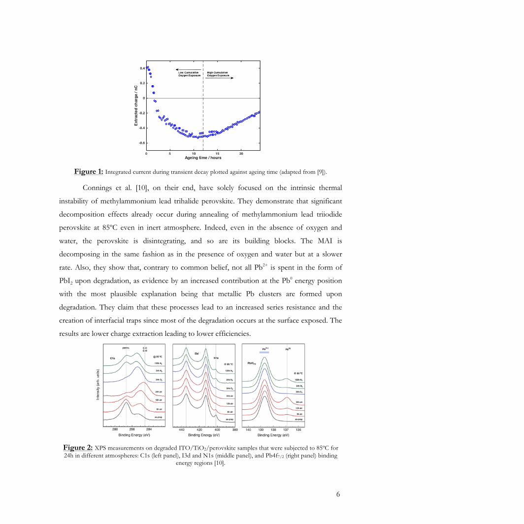
Indeed, Pearson et al. [9] focused on studying the kinetics and mechanics of oxygen
degradation of mesoporous Al2O3/CH3NH3PbI3-xClx perovskite solar cells. They have
observed that the degradation of the cells occurred under operation even in dry conditions
resulting in the decomposition of the perovskite itself. Specifically, it was proposed that
photogenerated electrons in the perovskite permit a reaction between the methylammonium
organic cation and superoxide, a process that results in the decomposition of CH3NH3PbI3
with methylamine, PbI2, I2, and H2O as byproducts:
CH3NH3PbI3+O2•-Deprotonation CH3NH2+PbI2+
12 I2+H2O
Transient photocurrent (TPC) and photovoltage (TPV) reveal that the degradation is related
to charge build-up in the perovskite layer. Specifically, they argue that photocurrent loss at
low cumulative oxygen exposure is due to the formation of charge barriers at the cell’s
electrode interface layer that act to screen the built-in field. Thereby, the efficiency of charge
extraction is reduced following the underlying mechanism of the increase of mobile defects
and electronic traps within the active layer. Then, at higher cumulative oxygen exposure, the
loss of photocurrent is due to material degradation more severe than just inducing defects
leading to decreased light harvesting efficiency and sub-microsecond recombination.
6
Figure 1: Integrated current during transient decay plotted against ageing time (adapted from [9]).
Connings et al. [10], on their end, have solely focused on the intrinsic thermal
instability of methylammonium lead trihalide perovskite. They demonstrate that significant
decomposition effects already occur during annealing of methylammonium lead triiodide
perovskite at 85ºC even in inert atmosphere. Indeed, even in the absence of oxygen and
water, the perovskite is disintegrating, and so are its building blocks. The MAI is
decomposing in the same fashion as in the presence of oxygen and water but at a slower
rate. Also, they show that, contrary to common belief, not all Pb2+ is spent in the form of
PbI2 upon degradation, as evidence by an increased contribution at the Pb0 energy position
with the most plausible explanation being that metallic Pb clusters are formed upon
degradation. They claim that these processes lead to an increased series resistance and the
creation of interfacial traps since most of the degradation occurs at the surface exposed. The
results are lower charge extraction leading to lower efficiencies.
Figure 2: XPS measurements on degraded ITO/TiO2/perovskite samples that were subjected to 85ºC for 24h in different atmospheres: C1s (left panel), I3d and N1s (middle panel), and Pb4f7/2 (right panel) binding
energy regions [10].
7
Figure 3: Photovoltaic parameters of solar cells prepared with perovskite layers that were subjected to a
temperature of 85ºC for 24h in different atmospheric conditions. The error bars reflect the standard deviation of a batch of four solar cells for each atmospheric condition [10].
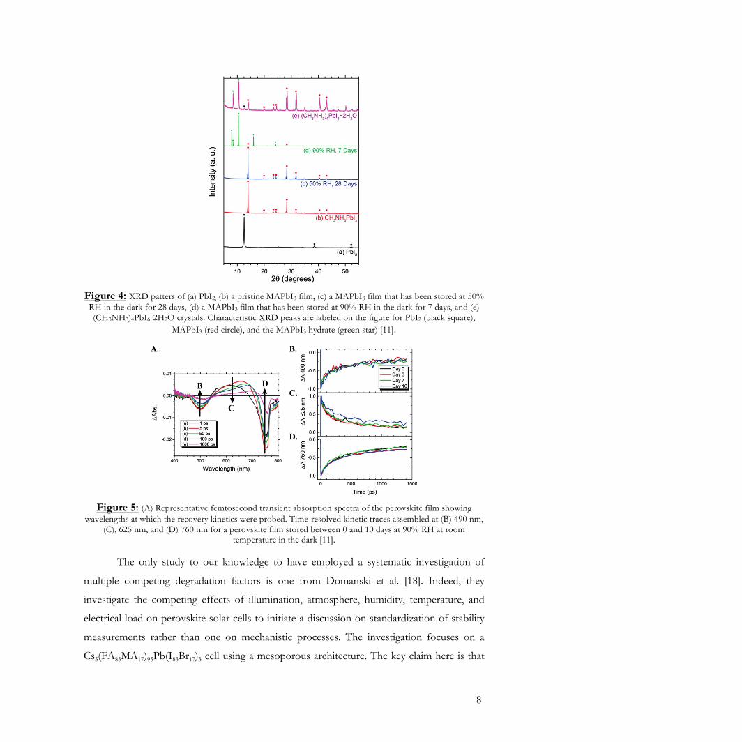
On their end, Christians et al. [11] have chosen to study humidity’s effect on MAPbI3
cells. They show that H2O exposure does not simply cause MAPbI3 to revert to PbI2, but it
also has the potential of forming a hydrate product similar to (CH3NH3)4PbI6•2H2O in the
dark as shown the XRD spectra. While significant changes are observed in the absorption
spectra, the presence of the hydrate has no significant effect on the charge carrier dynamics
at short times, which could be rationalized by the fact that defects in the MAPbI3 crystal
lattice tend to form only shallow trap states, while trap-mediated recombination mechanisms
are essentially absent on the nanosecond time scale [12]–[17]. The IV characteristics, on the
other hand, decrease sharply, and they hypothesize that the drop in long-range charge
transport is due to weak hydrogen-bonding interaction between the organic cation and the
metal halide octahedral and/or the strong hydrogen interaction between the organic cation
and H2O.
8
Figure 4: XRD patters of (a) PbI2, (b) a pristine MAPbI3 film, (c) a MAPbI3 film that has been stored at 50%
RH in the dark for 28 days, (d) a MAPbI3 film that has been stored at 90% RH in the dark for 7 days, and (e) (CH3NH3)4PbI6·2H2O crystals. Characteristic XRD peaks are labeled on the figure for PbI2 (black square),
MAPbI3 (red circle), and the MAPbI3 hydrate (green star) [11].
Figure 5: (A) Representative femtosecond transient absorption spectra of the perovskite film showing
wavelengths at which the recovery kinetics were probed. Time-resolved kinetic traces assembled at (B) 490 nm, (C), 625 nm, and (D) 760 nm for a perovskite film stored between 0 and 10 days at 90% RH at room
temperature in the dark [11]. The only study to our knowledge to have employed a systematic investigation of
multiple competing degradation factors is one from Domanski et al. [18]. Indeed, they
investigate the competing effects of illumination, atmosphere, humidity, temperature, and
electrical load on perovskite solar cells to initiate a discussion on standardization of stability
measurements rather than one on mechanistic processes. The investigation focuses on a
Cs5(FA83MA17)95Pb(I83Br17)3 cell using a mesoporous architecture. The key claim here is that
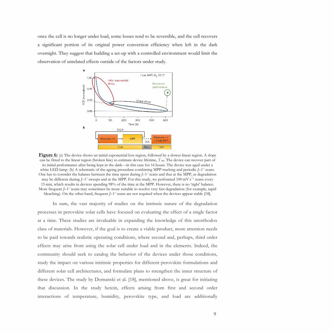
9
once the cell is no longer under load, some losses tend to be reversible, and the cell recovers
a significant portion of its original power conversion efficiency when left in the dark
overnight. They suggest that building a set-up with a controlled environment would limit the
observation of unrelated effects outside of the factors under study.
Figure 6: (a) The device shows an initial exponential loss region, followed by a slower linear region. A slope can be fitted to the linear region (broken line) to estimate device lifetime, T 80. The device can recover part of
its initial performance after being kept in the dark—in this case for 16 hours. The device was aged under a white LED lamp. (b) A schematic of the ageing procedure combining MPP tracking and periodic J–V scans.
One has to consider the balance between the time spent during J–V scans and that at the MPP, as degradation may be different during J–V sweeps and at the MPP. For this study, we performed 100 mV s−1 scans every 15 min, which results in devices spending 98% of the time at the MPP. However, there is no ‘right’ balance.
More frequent J–V scans may sometimes be more suitable to resolve very fast degradation (for example, rapid bleaching). On the other hand, frequent J–V scans are not required when the devices appear stable [18].
In sum, the vast majority of studies on the intrinsic nature of the degradation
processes in perovskite solar cells have focused on evaluating the effect of a single factor
at a time. These studies are invaluable in expanding the knowledge of this unorthodox
class of materials. However, if the goal is to create a viable product, more attention needs
to be paid towards realistic operating conditions, where second and, perhaps, third order
effects may arise from using the solar cell under load and in the elements. Indeed, the
community should seek to catalog the behavior of the devices under those conditions,
study the impact on various intrinsic properties for different perovskite formulations and
different solar cell architectures, and formulate plans to strengthen the inner structure of
these devices. The study by Domanski et al. [18], mentioned above, is great for initiating
that discussion. In the study herein, effects arising from first and second order
interactions of temperature, humidity, perovskite type, and load are additionally
10
systematically evaluated during degradation. These experiments are building blocks upon
which further investigation of the microstructure of the solar cell will potentially lead to
major improvements in stability.
Experimental Details:
Sample Preparation
FTO coated glass (7Ω/sq) purchased from MSE supplies were used as substrates for
the solar cells. The substrates were successively cleaned in (1) a 2% mixture of Hellmanex
(Sigma-Aldrich) in DI water, (2) acetone, and (3) isopropanol for 5min each in a sonicator.
They were then exposed for 3 min under oxygen plasma prior to spinning the electron
transport layer. The electron transport layer was prepared from (1) a titanium isopropoxide
solution purchased from Solaronix to form the compact TiO2 and (2) a colloidal dispersion
of TiO2 nanoparticles of <50nm also purchased from Solaronix. The hole transport material
precursor was prepared from a solution of spiro-OMeTAD (Sigma-Aldrich, 288mg) in
chlorobenzene (Sigma-Aldrich, 4mL) and doped with a 520mg/mL solution of
bis(trifluoromethane)sulfonimide lithium in acetonitrile (Sigma-Aldrich, 70µL) and 4-tert-
Butylphenol (Sigma-Aldrich, 115.2µL).
Perovskite Precursor Preparation Two different perovskite precursors were prepared for this study. The Cs0.2FA0.8PbI3
precursor was prepared from a solution of CsI (187mg), FAI (495mg), and PbI2 (1626mg) in
a 1:9 ratio of DMF (3.24mL) to DMSO (0.36mL). The solution was then stirred until
complete homogeneity. The MAPbI3 precursor was prepared from a solution of CH3NH3I
(395mg) and PbI2 (1153mg) in a 1:9 ratio of DMF (2.25mL) to DMSO (0.25mL). The
solution was then stirred until complete homogeneity. All reagents were purchased from
Sigma-Aldrich.
Solar Cell Fabrication First, under low humidity conditions, 100µL of the titanium isopropoxide precursor
was spun on the FTO substrates at 5000rpm and 2000rpm/s for 30s. They were then dried
at 150ºC for 10min of a hotplate followed by sintering under atmospheric conditions at
500ºC for 30min in a furnace to form the TiO2 blocking layer. After the substrates have
cooled down to room temperature and under atmospheric conditions, the colloidal
11
dispersion of TiO2 nanoparticles was spun on top of the blocking layer at 5000rpm and
2000rpm/s for 30s. They were then dried at 150ºC for 2min of a hotplate followed by a
sintering at 475ºC for 30min in a furnace to form the TiO2 mesoporous layer. The substrates
were moved to an N2 environment for the deposition of the perovskite layer. The 100µL of
perovskite precursor was spun for step 1 at 1000rpm/s and 500rpm/s for 10s and for step 2
at 6000rpm and 3000rpm/s for 25s. At 10s within step 2, droplets of cholorobenzene were
deposited at a rate of 1mL/min for a total volume of 100µL. The perovskite was then
annealed for 10min at 100ºC on a hotplate to form the perovskite active layer. Once cooled
back to room temperature, the solution of spiro-OmeTAD in cholorobenzene was spun on
top of the stack at 4000rpm and 2000rpm/s for 30s to form the hole transport material.
Finally, 80nm of Au were thermally evaporated to form the contacts. The active area,
defined as the overlap between the FTO and Au contacts, is 0.05cm2. The fabrication
process was adapted from a report by Yi et al. [19].
Measurements and Degradation Set-up The essence of this study is to understand the degradation of solar performance in
settings that reflect as much as possible realistic conditions. Indeed, the temperature bounds
chosen reflect room temperature (25ºC) and the highest ever recorded temperature on Earth
(55ºC), whereas the humidity levels chosen (30% and 60%) reflect levels typically
encountered in the Bay Area. In addition, two perovskite formulations and loading
conditions were chosen. Changing all these factors simultaneously allows for the extraction
of effects arising from interactions between factors that would be difficult to see otherwise
but does reflect how nature works. The various combinations employed are summarized in
Table 1.
12
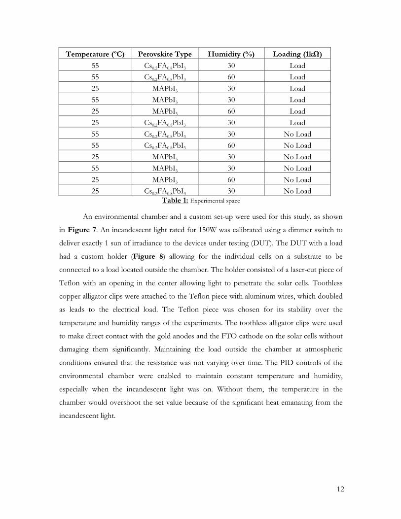
Temperature (ºC) Perovskite Type Humidity (%) Loading (1kΩ)
55 Cs0.2FA0.8PbI3 30 Load 55 Cs0.2FA0.8PbI3 60 Load 25 MAPbI3 30 Load 55 MAPbI3 30 Load 25 MAPbI3 60 Load 25 Cs0.2FA0.8PbI3 30 Load 55 Cs0.2FA0.8PbI3 30 No Load 55 Cs0.2FA0.8PbI3 60 No Load 25 MAPbI3 30 No Load 55 MAPbI3 30 No Load 25 MAPbI3 60 No Load 25 Cs0.2FA0.8PbI3 30 No Load
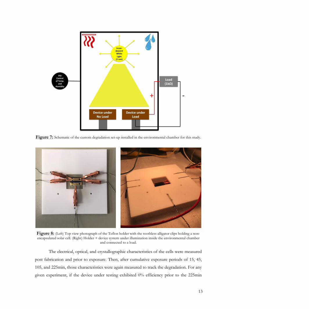
Table 1: Experimental space An environmental chamber and a custom set-up were used for this study, as shown
in Figure 7. An incandescent light rated for 150W was calibrated using a dimmer switch to
deliver exactly 1 sun of irradiance to the devices under testing (DUT). The DUT with a load
had a custom holder (Figure 8) allowing for the individual cells on a substrate to be
connected to a load located outside the chamber. The holder consisted of a laser-cut piece of
Teflon with an opening in the center allowing light to penetrate the solar cells. Toothless
copper alligator clips were attached to the Teflon piece with aluminum wires, which doubled
as leads to the electrical load. The Teflon piece was chosen for its stability over the
temperature and humidity ranges of the experiments. The toothless alligator clips were used
to make direct contact with the gold anodes and the FTO cathode on the solar cells without
damaging them significantly. Maintaining the load outside the chamber at atmospheric
conditions ensured that the resistance was not varying over time. The PID controls of the
environmental chamber were enabled to maintain constant temperature and humidity,
especially when the incandescent light was on. Without them, the temperature in the
chamber would overshoot the set value because of the significant heat emanating from the
incandescent light.
13
Figure 7: Schematic of the custom degradation set-up installed in the environmental chamber for this study.
Figure 8: (Left) Top view photograph of the Teflon holder with the toothless alligator clips holding a non-encapsulated solar cell. (Right) Holder + device system under illumination inside the environmental chamber
and connected to a load. The electrical, optical, and crystallographic characteristics of the cells were measured
post fabrication and prior to exposure. Then, after cumulative exposure periods of 15, 45,
105, and 225min, those characteristics were again measured to track the degradation. For any
given experiment, if the device under testing exhibited 0% efficiency prior to the 225min
Incan-descentWhiteLight(1sun)
DeviceunderLoad
DeviceunderNoLoad
PIDControlofTemp.
andHumidity
Load(1kΩ)
+ -
14
cumulative exposure period, the run was cut short. For each experiment a control cell was
kept in a N2 environment and measured at the same periodicity as the devices under testing.
The electrical characteristics were measured using a solar simulator delivering an AM1.5
spectrum at 100mW/cm2 and a Keithley-2400. To ensure the validity of the data collected,
the standard solar simulator set-up was improved to limit unnecessary light exposure and
speed up the measurements by fully automating the process. Indeed, while performing
steady state measurements on cells located on the same substrate, we have noticed that the
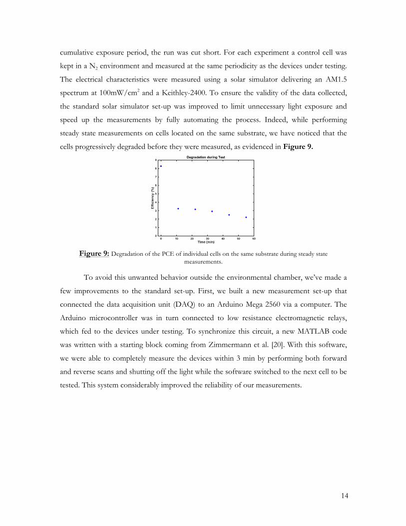
cells progressively degraded before they were measured, as evidenced in Figure 9.
Figure 9: Degradation of the PCE of individual cells on the same substrate during steady state
measurements. To avoid this unwanted behavior outside the environmental chamber, we’ve made a
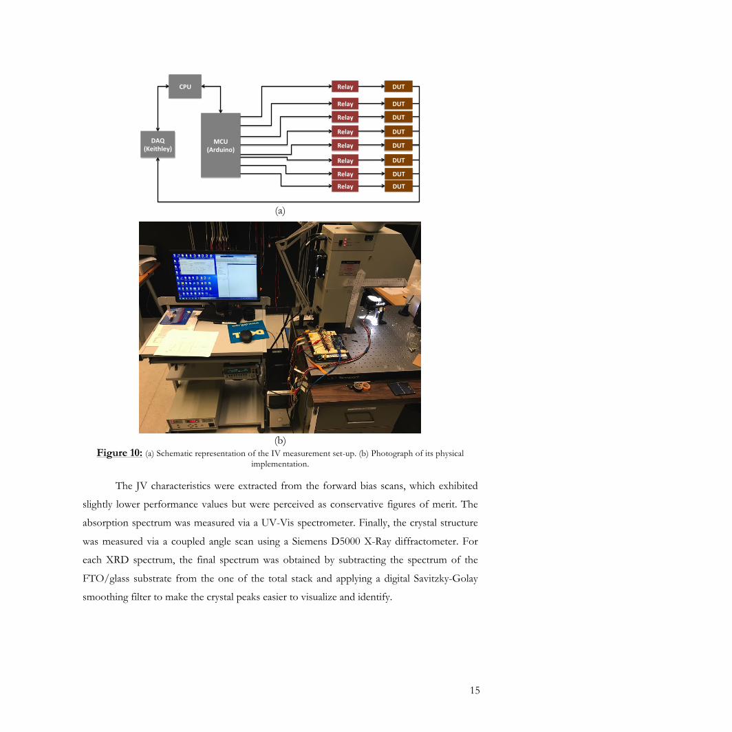
few improvements to the standard set-up. First, we built a new measurement set-up that
connected the data acquisition unit (DAQ) to an Arduino Mega 2560 via a computer. The
Arduino microcontroller was in turn connected to low resistance electromagnetic relays,
which fed to the devices under testing. To synchronize this circuit, a new MATLAB code
was written with a starting block coming from Zimmermann et al. [20]. With this software,
we were able to completely measure the devices within 3 min by performing both forward
and reverse scans and shutting off the light while the software switched to the next cell to be
tested. This system considerably improved the reliability of our measurements.
15
(a)
(b)
Figure 10: (a) Schematic representation of the IV measurement set-up. (b) Photograph of its physical implementation.
The JV characteristics were extracted from the forward bias scans, which exhibited
slightly lower performance values but were perceived as conservative figures of merit. The
absorption spectrum was measured via a UV-Vis spectrometer. Finally, the crystal structure
was measured via a coupled angle scan using a Siemens D5000 X-Ray diffractometer. For
each XRD spectrum, the final spectrum was obtained by subtracting the spectrum of the
FTO/glass substrate from the one of the total stack and applying a digital Savitzky-Golay
smoothing filter to make the crystal peaks easier to visualize and identify.
CPU
DAQ(Keithley)
MCU(Arduino) DUT
DUT
DUT
DUT
DUT
DUT
DUT
DUTRelay
Relay
Relay
Relay
Relay
Relay
Relay
Relay
16
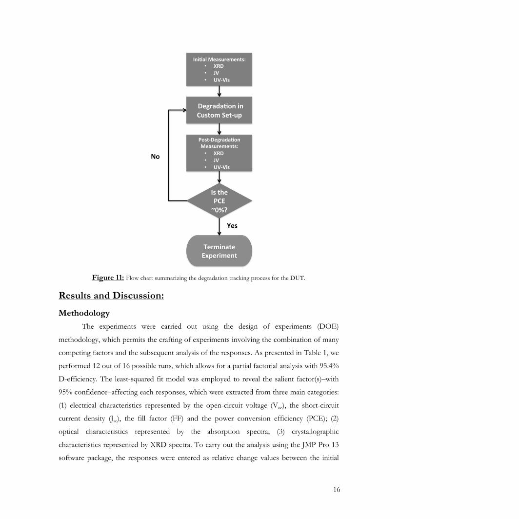
Figure 11: Flow chart summarizing the degradation tracking process for the DUT.
Results and Discussion:
Methodology The experiments were carried out using the design of experiments (DOE)
methodology, which permits the crafting of experiments involving the combination of many
competing factors and the subsequent analysis of the responses. As presented in Table 1, we
performed 12 out of 16 possible runs, which allows for a partial factorial analysis with 95.4%
D-efficiency. The least-squared fit model was employed to reveal the salient factor(s)–with
95% confidence–affecting each responses, which were extracted from three main categories:
(1) electrical characteristics represented by the open-circuit voltage (Voc), the short-circuit
current density (Jsc), the fill factor (FF) and the power conversion efficiency (PCE); (2)
optical characteristics represented by the absorption spectra; (3) crystallographic
characteristics represented by XRD spectra. To carry out the analysis using the JMP Pro 13
software package, the responses were entered as relative change values between the initial
Ini$alMeasurements:• XRD• JV• UV-Vis
Degrada$oninCustomSet-up
Post-Degrada$onMeasurements:• XRD• JV• UV-Vis
IsthePCE~0%?
TerminateExperiment
No
Yes
17
recorded characteristics of a cell and its measured characteristics by the end of run after
225min of cumulative exposure. Specifically, it meant that the responses were:
• For the electrical characteristics, !!!" = !!!"!"#!!!!"#!!!"#
; !!!" = !!!"!"#!!!!"#!!!"#
;
!!! = !!!!"!"# − !!!!"#!!!!"#
; !!"# = !"#!!"!"# − !"#!!"#!"#!!"#
• For the optical characteristics, the integrated absorption spectrum from 300nm to
900nm: !"#. !"#.= !"# !"!""!"!""!" ;! !"#. !"#. = !"#.!!". !!"!"#! !"#.!"#. !!"#
!"#.!"#. !!"#
• For the crystallographic characteristics, the full width at half maximum (FWHM) at
each salient peak: !"#$%(2!) = !"#$ !! !!"!"#!!"#$ !! !!"#!"#$ !! !!"#
To ensure the statistical significance of the data, the responses were weighed against
the controls by subtracting any relative change observed on the control cells from the
corresponding relative change observed on the devices under testing (DUT); that is,
!"#$%&'$# = !"#$ − !"#$%&#' . This methodology ensures that the effects observed are
purely due to the conditions of the experiments and not any other uncontrolled background
effect.
Effects on the Absorption Spectrum The analysis reveals that temperature is the only statistically significant factor in the
degradation of the absorption of the cells observed. Figure 12 shows a side-by-side view of
a MAPbI3 cell where the only factor changing is the temperature. The cell on the left shows
a progressive drop in total absorption located in the 300 to 500nm range of the wavelength
spectrum. On the other hand, the cell on the right shows a significant decrease in absorption
from 300 nm to the absorption edge at ~770nm, especially after 225min of cumulative
exposure period.
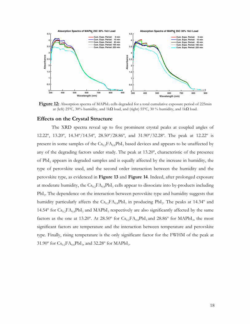
18
Figure 12: Absorption spectra of MAPbI3 cells degraded for a total cumulative exposure period of 225min
at (left) 25ºC, 30% humidity, and 1kΩ load, and (right) 55ºC, 30 % humidity, and 1kΩ load.
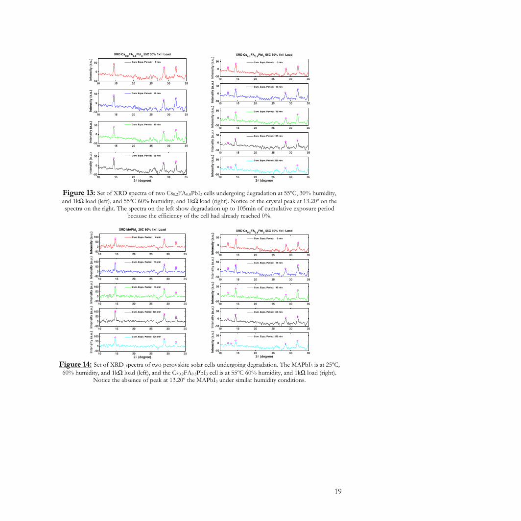
Effects on the Crystal Structure The XRD spectra reveal up to five prominent crystal peaks at coupled angles of
12.22º, 13.20º, 14.34º/14.54º, 28.50º/28.86º, and 31.90º/32.28º. The peak at 12.22º is
present in some samples of the Cs0.2FA0.8PbI3 based devices and appears to be unaffected by
any of the degrading factors under study. The peak at 13.20º, characteristic of the presence
of PbI2 appears in degraded samples and is equally affected by the increase in humidity, the
type of perovskite used, and the second order interaction between the humidity and the
perovskite type, as evidenced in Figure 13 and Figure 14. Indeed, after prolonged exposure
at moderate humidity, the Cs0.2FA0.8PbI3 cells appear to dissociate into by-products including
PbI2. The dependence on the interaction between perovskite type and humidity suggests that
humidity particularly affects the Cs0.2FA0.8PbI3 in producing PbI2. The peaks at 14.34º and
14.54º for Cs0.2FA0.8PbI3 and MAPbI3 respectively are also significantly affected by the same
factors as the one at 13.20º. At 28.50º for Cs0.2FA0.8PbI3 and 28.86º for MAPbI3, the most
significant factors are temperature and the interaction between temperature and perovskite
type. Finally, rising temperature is the only significant factor for the FWHM of the peak at
31.90º for Cs0.2FA0.8PbI3, and 32.28º for MAPbI3.
300 400 500 600 700 800 900Wavelength (nm)
0
0.5
1
1.5
2
2.5
3
3.5
4
4.5
Abs
orba
nce
Absorption Spectra of MAPbI3 25C 30% 1k Load
Cum. Expo. Period: 0 minCum. Expo. Period: 15 minCum. Expo. Period: 45 minCum. Expo. Period: 105 minCum. Expo. Period: 225 min
300 400 500 600 700 800 900Wavelength (nm)
0
0.5
1
1.5
2
2.5
3
3.5
4
4.5
Abs
orba
nce
Absorption Spectra of MAPbI3 55C 30% 1k Load
Cum. Expo. Period: 0 minCum. Expo. Period: 15 minCum. Expo. Period: 45 minCum. Expo. Period: 105 minCum. Expo. Period: 225 min
19
Figure 13: Set of XRD spectra of two Cs0.2FA0.8PbI3 cells undergoing degradation at 55ºC, 30% humidity, and 1kΩ load (left), and 55ºC 60% humidity, and 1kΩ load (right). Notice of the crystal peak at 13.20º on the spectra on the right. The spectra on the left show degradation up to 105min of cumulative exposure period
because the efficiency of the cell had already reached 0%.
Figure 14: Set of XRD spectra of two perovskite solar cells undergoing degradation. The MAPbI3 is at 25ºC,
60% humidity, and 1kΩ load (left), and the Cs0.2FA0.8PbI3 cell is at 55ºC 60% humidity, and 1kΩ load (right). Notice the absence of peak at 13.20º the MAPbI3 under similar humidity conditions.
XRD Cs0.2FA0.8PbI3 55C 30% 1k+ Load
10 15 20 25 30 35
Inte
nsity
(a.u
.)
-50
0
50 Cum. Expo. Period: 0 min
10 15 20 25 30 35
Inte
nsity
(a.u
.)
-50
0
50 Cum. Expo. Period: 15 min
10 15 20 25 30 35
Inte
nsity
(a.u
.)
-50
0
50 Cum. Expo. Period: 45 min
23 (degree)10 15 20 25 30 35
Inte
nsity
(a.u
.)
-50
0
50 Cum. Expo. Period: 105 min
XRD Cs0.2FA0.8PbI3 55C 60% 1k+ Load
10 15 20 25 30 35Inte
nsity
(a.u
.)
-50
0
50 Cum. Expo. Period: 0 min
10 15 20 25 30 35Inte
nsity
(a.u
.)
-50
0
50 Cum. Expo. Period: 15 min
10 15 20 25 30 35Inte
nsity
(a.u
.)
-50
0
50 Cum. Expo. Period: 45 min
10 15 20 25 30 35Inte
nsity
(a.u
.)
-50
0
50 Cum. Expo. Period: 105 min
23 (degree)10 15 20 25 30 35In
tens
ity (a
.u.)
-50
0
50 Cum. Expo. Period: 225 min
XRD MAPbI3 25C 60% 1k+ Load
10 15 20 25 30 35Inte
nsity
(a.u
.)
-500
50100 Cum. Expo. Period: 0 min
10 15 20 25 30 35Inte
nsity
(a.u
.)
-500
50100 Cum. Expo. Period: 15 min
10 15 20 25 30 35Inte
nsity
(a.u
.)
-500
50100 Cum. Expo. Period: 45 min
10 15 20 25 30 35Inte
nsity
(a.u
.)
-500
50100 Cum. Expo. Period: 105 min
23 (degree)10 15 20 25 30 35In
tens
ity (a
.u.)
-500
50100 Cum. Expo. Period: 225 min
XRD Cs0.2FA0.8PbI3 55C 60% 1k+ Load
10 15 20 25 30 35Inte
nsity
(a.u
.)
-50
0
50 Cum. Expo. Period: 0 min
10 15 20 25 30 35Inte
nsity
(a.u
.)
-50
0
50 Cum. Expo. Period: 15 min
10 15 20 25 30 35Inte
nsity
(a.u
.)
-50
0
50 Cum. Expo. Period: 45 min
10 15 20 25 30 35Inte
nsity
(a.u
.)
-50
0
50 Cum. Expo. Period: 105 min
23 (degree)10 15 20 25 30 35In
tens
ity (a
.u.)
-50
0
50 Cum. Expo. Period: 225 min
20
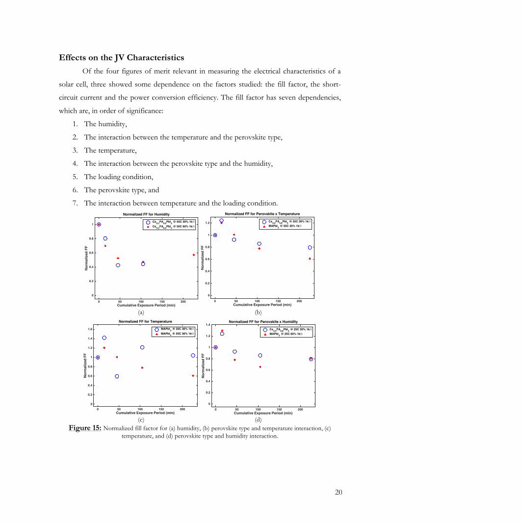
Effects on the JV Characteristics Of the four figures of merit relevant in measuring the electrical characteristics of a
solar cell, three showed some dependence on the factors studied: the fill factor, the short-
circuit current and the power conversion efficiency. The fill factor has seven dependencies,
which are, in order of significance:
1. The humidity,
2. The interaction between the temperature and the perovskite type,
3. The temperature,
4. The interaction between the perovskite type and the humidity,
5. The loading condition,
6. The perovskite type, and
7. The interaction between temperature and the loading condition.
(a) (b)
(c) (d)
Figure 15: Normalized fill factor for (a) humidity, (b) perovskite type and temperature interaction, (c) temperature, and (d) perovskite type and humidity interaction.
Cumulative Exposure Period (min)0 50 100 150 200
Nor
mal
ized
FF
0
0.2
0.4
0.6
0.8
1
Normalized FF for Humidity
Cs0.2FA0.8PbI3 @ 55C 30% 1k+Cs0.2FA0.8PbI3 @ 55C 60% 1k+
Cumulative Exposure Period (min)0 50 100 150 200
Nor
mal
ized
FF
0
0.2
0.4
0.6
0.8
1
1.2
Normalized FF for Perovskite x Temperature
Cs0.2FA0.8PbI3 @ 25C 30% 1k+MAPbI3 @ 55C 30% 1k+
Cumulative Exposure Period (min)0 50 100 150 200
Nor
mal
ized
FF
0
0.2
0.4
0.6
0.8
1
1.2
1.4
1.6
Normalized FF for Temperature
MAPbI3 @ 25C 30% 1k+MAPbI3 @ 55C 30% 1k+
Cumulative Exposure Period (min)0 50 100 150 200
Nor
mal
ized
FF
0
0.2
0.4
0.6
0.8
1
1.2
1.4Normalized FF for Perovskite x Humidity
Cs0.2FA0.8PbI3 @ 25C 30% 1k+MAPbI3 @ 25C 60% 1k+
21
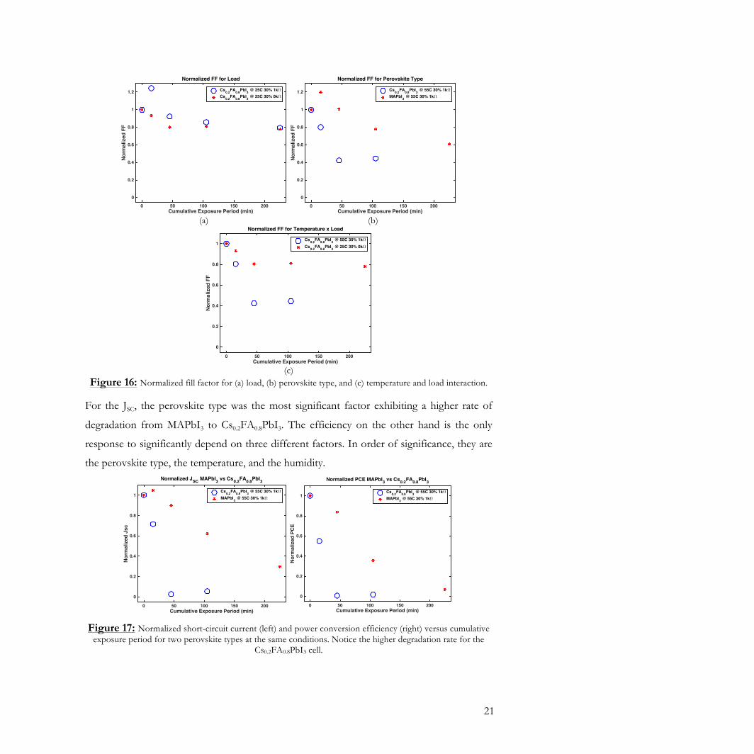
(a) (b)
(c)
Figure 16: Normalized fill factor for (a) load, (b) perovskite type, and (c) temperature and load interaction. For the JSC, the perovskite type was the most significant factor exhibiting a higher rate of
degradation from MAPbI3 to Cs0.2FA0.8PbI3. The efficiency on the other hand is the only
response to significantly depend on three different factors. In order of significance, they are
the perovskite type, the temperature, and the humidity.
Figure 17: Normalized short-circuit current (left) and power conversion efficiency (right) versus cumulative
exposure period for two perovskite types at the same conditions. Notice the higher degradation rate for the Cs0.2FA0.8PbI3 cell.
Cumulative Exposure Period (min)0 50 100 150 200
Nor
mal
ized
FF
0
0.2
0.4
0.6
0.8
1
1.2
Normalized FF for Load
Cs0.2FA0.8PbI3 @ 25C 30% 1k+Cs0.2FA0.8PbI3 @ 25C 30% 0k+
Cumulative Exposure Period (min)0 50 100 150 200
Nor
mal
ized
FF
0
0.2
0.4
0.6
0.8
1
1.2
Normalized FF for Perovskite Type
Cs0.2FA0.8PbI3 @ 55C 30% 1k+MAPbI3 @ 55C 30% 1k+
Cumulative Exposure Period (min)0 50 100 150 200
Nor
mal
ized
FF
0
0.2
0.4
0.6
0.8
1
Normalized FF for Temperature x Load
Cs0.2FA0.8PbI3 @ 55C 30% 1k+Cs0.2FA0.8PbI3 @ 25C 30% 0k+
Cumulative Exposure Period (min)0 50 100 150 200
Nor
mal
ized
Jsc
0
0.2
0.4
0.6
0.8
1
Normalized JSC MAPbI3 vs Cs0.2FA0.8PbI3
Cs0.2FA0.8PbI3 @ 55C 30% 1k+MAPbI3 @ 55C 30% 1k+
Cumulative Exposure Period (min)0 50 100 150 200
Nor
mal
ized
PC
E
0
0.2
0.4
0.6
0.8
1
Normalized PCE MAPbI3 vs Cs0.2FA0.8PbI3
Cs0.2FA0.8PbI3 @ 55C 30% 1k+MAPbI3 @ 55C 30% 1k+
22
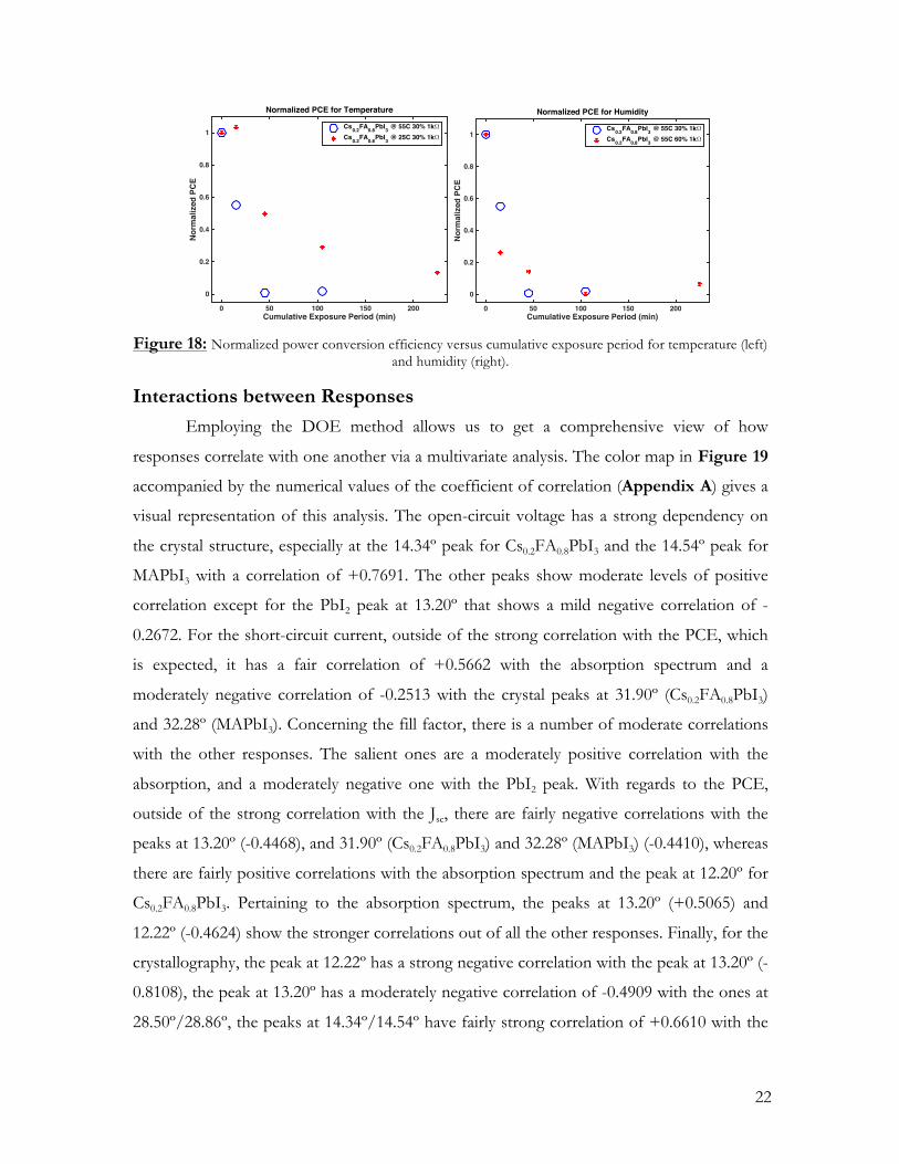
Figure 18: Normalized power conversion efficiency versus cumulative exposure period for temperature (left)
and humidity (right).
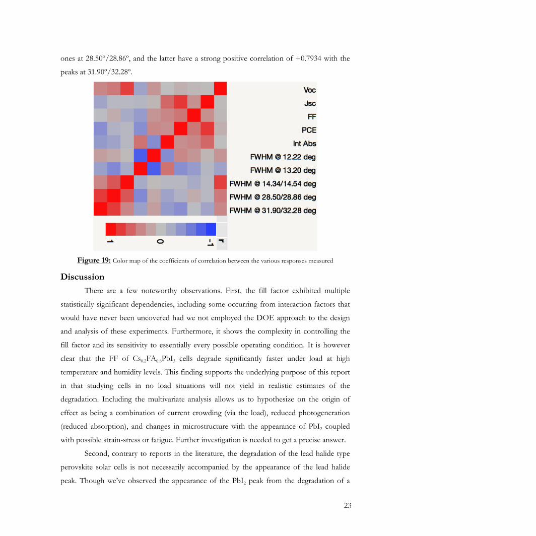
Interactions between Responses Employing the DOE method allows us to get a comprehensive view of how
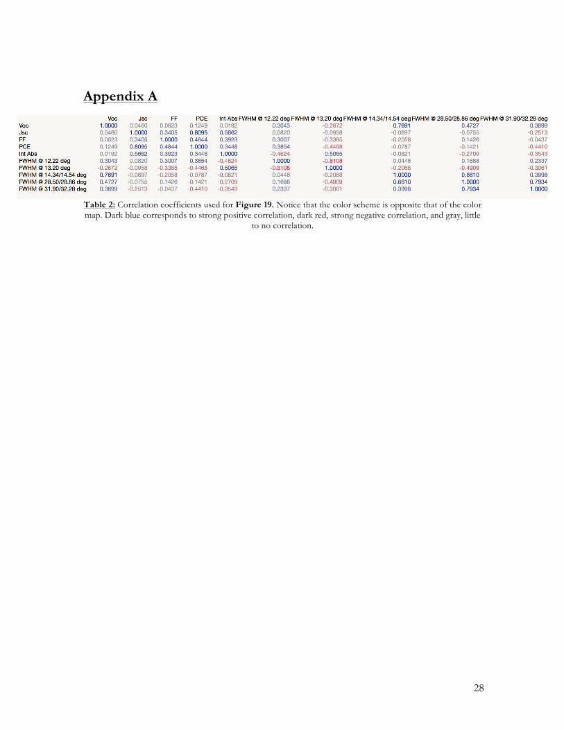
responses correlate with one another via a multivariate analysis. The color map in Figure 19
accompanied by the numerical values of the coefficient of correlation (Appendix A) gives a
visual representation of this analysis. The open-circuit voltage has a strong dependency on
the crystal structure, especially at the 14.34º peak for Cs0.2FA0.8PbI3 and the 14.54º peak for
MAPbI3 with a correlation of +0.7691. The other peaks show moderate levels of positive
correlation except for the PbI2 peak at 13.20º that shows a mild negative correlation of -
0.2672. For the short-circuit current, outside of the strong correlation with the PCE, which
is expected, it has a fair correlation of +0.5662 with the absorption spectrum and a
moderately negative correlation of -0.2513 with the crystal peaks at 31.90º (Cs0.2FA0.8PbI3)
and 32.28º (MAPbI3). Concerning the fill factor, there is a number of moderate correlations
with the other responses. The salient ones are a moderately positive correlation with the
absorption, and a moderately negative one with the PbI2 peak. With regards to the PCE,
outside of the strong correlation with the Jsc, there are fairly negative correlations with the
peaks at 13.20º (-0.4468), and 31.90º (Cs0.2FA0.8PbI3) and 32.28º (MAPbI3) (-0.4410), whereas
there are fairly positive correlations with the absorption spectrum and the peak at 12.20º for
Cs0.2FA0.8PbI3. Pertaining to the absorption spectrum, the peaks at 13.20º (+0.5065) and
12.22º (-0.4624) show the stronger correlations out of all the other responses. Finally, for the
crystallography, the peak at 12.22º has a strong negative correlation with the peak at 13.20º (-
0.8108), the peak at 13.20º has a moderately negative correlation of -0.4909 with the ones at
28.50º/28.86º, the peaks at 14.34º/14.54º have fairly strong correlation of +0.6610 with the
Cumulative Exposure Period (min)0 50 100 150 200
Nor
mal
ized
PC
E
0
0.2
0.4
0.6
0.8
1
Normalized PCE for Temperature
Cs0.2FA0.8PbI3 @ 55C 30% 1k+Cs0.2FA0.8PbI3 @ 25C 30% 1k+
Cumulative Exposure Period (min)0 50 100 150 200
Nor
mal
ized
PC
E
0
0.2
0.4
0.6
0.8
1
Normalized PCE for Humidity
Cs0.2FA0.8PbI3 @ 55C 30% 1k+Cs0.2FA0.8PbI3 @ 55C 60% 1k+
23
ones at 28.50º/28.86º, and the latter have a strong positive correlation of +0.7934 with the
peaks at 31.90º/32.28º.
Figure 19: Color map of the coefficients of correlation between the various responses measured
Discussion There are a few noteworthy observations. First, the fill factor exhibited multiple
statistically significant dependencies, including some occurring from interaction factors that
would have never been uncovered had we not employed the DOE approach to the design
and analysis of these experiments. Furthermore, it shows the complexity in controlling the
fill factor and its sensitivity to essentially every possible operating condition. It is however
clear that the FF of Cs0.2FA0.8PbI3 cells degrade significantly faster under load at high
temperature and humidity levels. This finding supports the underlying purpose of this report
in that studying cells in no load situations will not yield in realistic estimates of the
degradation. Including the multivariate analysis allows us to hypothesize on the origin of
effect as being a combination of current crowding (via the load), reduced photogeneration
(reduced absorption), and changes in microstructure with the appearance of PbI2 coupled
with possible strain-stress or fatigue. Further investigation is needed to get a precise answer.
Second, contrary to reports in the literature, the degradation of the lead halide type
perovskite solar cells is not necessarily accompanied by the appearance of the lead halide
peak. Though we’ve observed the appearance of the PbI2 peak from the degradation of a
24
Cs0.2FA0.8PbI3 cell at 55ºC and 60% humidity, it was the only such case. All the other cells
reached their operational limit without any observable appearance of the PbI2 peak.
However, the loss in PCE is accompanied by an increase in FWHM (broader peaks) with
increased humidity at some angles, and a decrease in FWHM (sharper peaks) with increased
temperature at other angles. These changes in FWHM could be indicative of a few intrinsic
processes occurring in the microstructure of the perovskites. It could indicate increased
fatigue, an increased strain-stress accumulation, a change in crystal size, and/or an increase
in density of point defects in the lattice. Follow up studies will illuminate the underlying
mechanism behind this peculiar observation.
Third, the loss in absorption due to temperature increase follows well the loss in
short-circuit current and efficiency as a function of temperature as well as the change in
crystal structure with temperature. The obvious connection is that the net reduction in
absorbed light causes a net loss of photogenerated carriers thus reducing the overall PCE.
However, semiconducting materials, like perovskites, usually generate more electron-hole
pairs with temperature without generating phonons, especially when they are direct band gap
materials. It is possible that one of the processes speculated above could be overshadowing
the thermal generation and recombination process.
Fourth, the open-circuit voltage did not show any statistically significant dependence
on any single factor studied. However, the Voc is observed to degrade over time, and the
multivariate analysis reveals a significant correlation to the changes in crystal structure.
Correlation is not causation, and this observation could just be a coincidence given that the
controlled factors that resulted in statistically significant dependence for the crystal structure
do not show the same relevance for the Voc. Nonetheless, it is possible that the timescale
under which the study was undertaken was too short to obtain a definitive result. Another
study may be required to answer this conundrum.
Finally, the loss of PCE due to humidity is a process covered ad nauseam in the
literature[21], [22]. However, the observations from our experiments show that, under
similar conditions, Cs0.2FA0.8PbI3 cells are less stable than the MAPbI3 cells. This is contrary
to multiple reports [23], [24] contending that a larger sized A-group in the ABX3 structure of
the perovskite–accomplished via hybridization of the Cs with FA–would result in more
stable solar devices. The evidence presented in these reports is quite compelling, so
duplicates of these experiments should be run to confirm this observation.
25
Conclusion: By controlling four factors (temperature, humidity, perovskite type, and electrical
load), the degradation of perovskite solar cells was investigated. A few key observations have
arisen as a consequence: (1) the fill factor of Cs0.2FA0.8PbI3 cells degrade significantly faster
under load at high temperature and humidity levels; (2) the loss in PCE does not necessarily
result in an appearance of a PbI2 peak in lead halide type perovskites, but could rather be
related to other changes in the microstructure; and (3) temperature is a strong degrading
element. Further studies are needed to confirm the trends observed and provide a more
mechanistic insight onto the stability issues of perovskite solar cells.
Acknowledgements: This work was made possible by a National Science Foundation Graduate Research
Fellowship, a Chancellor’s Fellowship, and a Jack Kent Cooke Foundation Graduate
Scholarship. Prof. Ana Arias’ gracefulness and generosity is applauded for sharing her lab
tools, which were critical in carrying out this study to completion. Thanks also go to my
collaborators Matthew McPhail and Lance Go for their considerable support. Jeremy Smith,
William Scheideler, and Gerd Grau are also hereby recognized for the insightful
conversations.
26
References: [1] A. Kojima, K. Teshima, Y. Shirai, and T. Miyasaka, “Organometal Halide Perovskites as Visible-Light
Sensitizers for Photovoltaic Cells,” J. Am. Chem. Soc., vol. 131, no. 17, pp. 6050–6051, May 2009.
[2] M. M. Lee, J. Teuscher, T. Miyasaka, T. N. Murakami, and H. J. Snaith, “Efficient hybrid solar cells based on meso-superstructured organometal halide perovskites.,” Science, vol. 338, no. 6107, pp. 643–7, Nov. 2012.
[3] NREL, “Best Research-Cell Efficiiencies,” 2017. [Online]. Available: https://www.nrel.gov/pv/assets/images/efficiency-chart.png. [Accessed: 04-Jan-2018].
[4] P. A. Basore, “Pilot production of thin-film crystalline silicon on glass modules,” in Conference Record of the Twenty-Ninth IEEE Photovoltaic Specialists Conference, 2002., pp. 49–52.
[5] A. Miyata, A. Mitioglu, P. Plochocka, O. Portugall, J. T.-W. Wang, S. D. Stranks, H. J. Snaith, and R. J. Nicholas, “Direct measurement of the exciton binding energy and effective masses for charge carriers in organic–inorganic tri-halide perovskites,” Nat. Phys., vol. 11, no. 7, pp. 582–587, Jul. 2015.
[6] W. Li, W. Zhang, S. Van Reenen, R. J. Sutton, J. Fan, A. A. Haghighirad, M. B. Johnston, L. Wang, and H. J. Snaith, “Enhanced UV-light stability of planar heterojunction perovskite solar cells with caesium bromide interface modification,” Energy Environ. Sci., vol. 9, no. 2, pp. 490–498, Feb. 2016.
[7] H. C. Weerasinghe, Y. Dkhissi, A. D. Scully, R. A. Caruso, and Y.-B. Cheng, “Encapsulation for improving the lifetime of flexible perovskite solar cells,” Nano Energy, vol. 18, pp. 118–125, Nov. 2015.
[8] G. Grancini, C. Roldán-Carmona, I. Zimmermann, E. Mosconi, X. Lee, D. Martineau, S. Narbey, F. Oswald, F. De Angelis, M. Graetzel, and M. K. Nazeeruddin, “One-Year stable perovskite solar cells by 2D/3D interface engineering,” Nat. Commun., vol. 8, p. 15684, Jun. 2017.
[9] A. J. Pearson, G. E. Eperon, P. E. Hopkinson, S. N. Habisreutinger, J. T.-W. Wang, H. J. Snaith, and N. C. Greenham, “Oxygen Degradation in Mesoporous Al2O3/CH3NH3PbI3-xClx Perovskite Solar Cells: Kinetics and Mechanisms,” Adv. Energy Mater., vol. 6, no. 13, p. 1600014, Jul. 2016.
[10] B. Conings, J. Drijkoningen, N. Gauquelin, A. Babayigit, J. D’Haen, L. D’Olieslaeger, A. Ethirajan, J. Verbeeck, J. Manca, E. Mosconi, F. De Angelis, and H.-G. Boyen, “Intrinsic Thermal Instability of Methylammonium Lead Trihalide Perovskite,” Adv. Energy Mater., vol. 5, no. 15, p. 1500477, Aug. 2015.
[11] J. A. Christians, P. A. Miranda Herrera, and P. V. Kamat, “Transformation of the Excited State and Photovoltaic Efficiency of CH3NH3PbI3 Perovskite upon Controlled Exposure to Humidified Air,” J. Am. Chem. Soc., vol. 137, no. 4, pp. 1530–1538, Feb. 2015.
[12] H. Oga, A. Saeki, Y. Ogomi, S. Hayase, and S. Seki, “Correction to Improved Understanding of the Electronic and Energetic Landscapes of Perovskite Solar Cells: High Local Charge Carrier Mobility, Reduced Recombination, and Extremely Shallow Traps,” J. Am. Chem. Soc., vol. 136, no. 48, pp. 16948–16948, Dec. 2014.
[13] H. Oga, A. Saeki, Y. Ogomi, S. Hayase, and S. Seki, “Improved Understanding of the Electronic and Energetic Landscapes of Perovskite Solar Cells: High Local Charge Carrier Mobility, Reduced Recombination, and Extremely Shallow Traps,” J. Am. Chem. Soc., vol. 136, no. 39, pp. 13818–13825, Oct. 2014.
[14] E. Edri, S. Kirmayer, A. Henning, S. Mukhopadhyay, K. Gartsman, Y. Rosenwaks, G. Hodes, and D. Cahen, “Why Lead Methylammonium Tri-Iodide Perovskite-Based Solar Cells Require a Mesoporous Electron Transporting Scaffold (but Not Necessarily a Hole Conductor),” Nano Lett., vol. 14, no. 2, pp. 1000–1004, Feb. 2014.
[15] W.-J. Yin, T. Shi, and Y. Yan, “Unusual defect physics in CH3NH3PbI3 perovskite solar cell absorber,” Appl. Phys. Lett., vol. 104, no. 6, p. 63903, Feb. 2014.
27
[16] C. Wehrenfennig, G. E. Eperon, M. B. Johnston, H. J. Snaith, and L. M. Herz, “High Charge Carrier Mobilities and Lifetimes in Organolead Trihalide Perovskites,” Adv. Mater., vol. 26, no. 10, pp. 1584–1589, Mar. 2014.
[17] J. S. Manser and P. V. Kamat, “Band filling with free charge carriers in organometal halide perovskites,” Nat. Photonics, vol. 8, no. 9, pp. 737–743, Sep. 2014.
[18] K. Domanski, E. A. Alharbi, A. Hagfeldt, M. Grätzel, and W. Tress, “Systematic investigation of the impact of operation conditions on the degradation behaviour of perovskite solar cells,” Nat. Energy, pp. 1–7, Jan. 2018.
[19] C. Yi, J. Luo, S. Meloni, A. Boziki, N. Ashari-Astani, C. Grätzel, S. M. Zakeeruddin, U. Röthlisberger, and M. Grätzel, “Entropic stabilization of mixed A-cation ABX3 metal halide perovskites for high performance perovskite solar cells,” Energy Environ. Sci., vol. 9, no. 2, pp. 656–662, Feb. 2016.
[20] E. Zimmermann, K. K. Wong, M. Müller, H. Hu, P. Ehrenreich, M. Kohlstädt, U. Würfel, S. Mastroianni, G. Mathiazhagan, A. Hinsch, T. P. Gujar, M. Thelakkat, T. Pfadler, and L. Schmidt-Mende, “Characterization of perovskite solar cells: Towards a reliable measurement protocol,” APL Mater., vol. 4, no. 9, p. 91901, Sep. 2016.
[21] B. Hailegnaw, S. Kirmayer, E. Edri, G. Hodes, and D. Cahen, “Rain on Methylammonium Lead Iodide Based Perovskites: Possible Environmental Effects of Perovskite Solar Cells,” J. Phys. Chem. Lett., vol. 6, no. 9, pp. 1543–1547, May 2015.
[22] E. Mosconi, J. M. Azpiroz, and F. De Angelis, “Ab Initio Molecular Dynamics Simulations of Methylammonium Lead Iodide Perovskite Degradation by Water,” Chem. Mater., vol. 27, no. 13, pp. 4885–4892, Jul. 2015.
[23] J.-W. Lee, D.-H. Kim, H.-S. Kim, S.-W. Seo, S. M. Cho, and N.-G. Park, “Formamidinium and Cesium Hybridization for Photo- and Moisture-Stable Perovskite Solar Cell,” Adv. Energy Mater., vol. 5, no. 20, p. 1501310, Oct. 2015.
[24] Z. Li, M. Yang, J.-S. Park, S.-H. Wei, J. J. Berry, and K. Zhu, “Stabilizing Perovskite Structures by Tuning Tolerance Factor: Formation of Formamidinium and Cesium Lead Iodide Solid-State Alloys,” Chem. Mater., vol. 28, no. 1, pp. 284–292, Jan. 2016.
28
Appendix A
Table 2: Correlation coefficients used for Figure 19. Notice that the color scheme is opposite that of the color map. Dark blue corresponds to strong positive correlation, dark red, strong negative correlation, and gray, little
to no correlation.


![Mechanistic Consideration for Thermal Degradation of ......2017/01/31 · thermal degradation of vinyl polymers, they corrected it by vaporization [16]. There does not exist a process](https://img.pdfslide.us/doc/110x75/606d9ce90099f96f162769d7/mechanistic-consideration-for-thermal-degradation-of-20170131-thermal.jpg)