Embed Size (px)
Citation preview
Doc. File TRNT-AD-08-0012 Torrent Sequencer Description R0.doc Created on 8/10/2012 Doc. Number TRNT-AD-08-0012
Page 1 of 18
TORRENT Sequencer Mpu Description
NOAO Document TRNT-AD-08-0012
Revision: 0
Authored by: Peter Moore
Please send comments: [email protected]
NATIONAL OPTICAL ASTRONOMY OBSERVATORY
SYSTEM INSTRUMENTATION GROUP 950 N. Cherry Ave.
P. O. Box 26732 Tucson, Arizona 85726-6732
(520) 318-8000 FAX: (520) 318-8303
Doc. File TRNT-AD-08-0012 Torrent Sequencer Description R0.doc Created on 8/10/2012 Doc. Number TRNT-AD-08-0012
Page 2 of 18
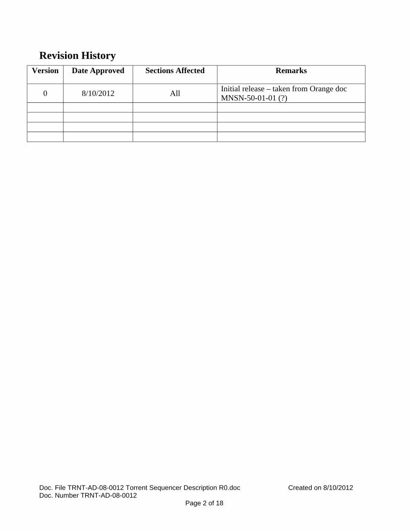
Revision History Version Date Approved Sections Affected Remarks
0 8/10/2012 All Initial release – taken from Orange doc MNSN-50-01-01 (?)
Doc. File TRNT-AD-08-0012 Torrent Sequencer Description R0.doc Created on 8/10/2012 Doc. Number TRNT-AD-08-0012
Page 3 of 18
Table of Contents Preface ................................................................................................................................ 5 Document Scope ................................................................................................................ 5 Introduction ....................................................................................................................... 5
Sequencer Performance ................................................................................................ 5 Sequencer Interface ...................................................................................................... 5
Architecture Overview ...................................................................................................... 7 Program Memory ............................................................................................................. 8 Pattern Memory ................................................................................................................ 8 Stacks ............................................................................................................................... 8 Decode Execution Unit (DEU) ........................................................................................ 9 Special Function Registers ............................................................................................. 11
Sequencer Run Enable register (SeqEnable attribute) ................................................ 11 DHE is a Slave register (DheIsSlave attribute) .......................................................... 11 Command register (SeqCmds attribute) ..................................................................... 11 Integration Time register (IntegrationTime attribute) ................................................ 12 Pause the Exposure register (PauseExposure attribute) .............................................. 13 Synchronize Command Delay register (SyncDelay attribute) .................................... 13 User Control Bits register (SeqUserBits attribute) ..................................................... 13 Sequencer Clock Divider register (SeqClkDivide attribute) ...................................... 13 Sequencer Status register (SeqStatus attribute) .......................................................... 13 Enable Flag register (SeqEFR attribute) ..................................................................... 13 Loop Control registers (SeqLoopReg(15:0) attribute) ............................................... 14
Instruction Set for the Sequencer .................................................................................. 15 Output Instructions ......................................................................................................... 15
LPP: Load Pattern Pointer: 4 Nibble (16 bit) ............................................................. 15 IPP: Increment Pattern Pointer: 1 Nibble (4-bit) ........................................................ 15 DPP: Decrement Pattern Pointer: 1 Nibble (4-bit) ..................................................... 16 LDA: Load Device Address (12-bit) .......................................................................... 16 LMR: Load Mode Register 3 Nibble (12-bit) ............................................................. 16 LSR: Load Select Register 3 Nibble (12-bit) ............................................................. 16
Control Instructions ........................................................................................................ 16 CAL: Call Subroutine: 4 Nibble (16 bit) .................................................................... 16 RET: Return 1 Nibble (4-bit) ...................................................................................... 17 JCB: Jump if Control Bit Set. 5 Nibble (20-bit) ......................................................... 17 LRB: Loop Begin 2 Nibble (8-bit) ............................................................................. 17 LPB: Loop Begin 1 Nibble (4-bit) .............................................................................. 17 LPE: Loop End 1 Nibble (4-bit) ................................................................................. 17
Delay Instructions .......................................................................................................... 18 DMS: Delay Milliseconds 3 Nibble (12-bit) .............................................................. 18 DUS: Delay Microseconds 3 Nibble (12-bit) ............................................................. 18 DSC: Delay System Clock 3 Nibble (12-bit) ............................................................. 18 NOP: No Operation 1 Nibble (4-bit) .......................................................................... 18
Doc. File TRNT-AD-08-0012 Torrent Sequencer Description R0.doc Created on 8/10/2012 Doc. Number TRNT-AD-08-0012
Page 4 of 18
List of Figures
Figure 1 – Sequencer Mpu interface symbol ....................................................................... 6 Figure 2 – Sequencer Mpu Architecture ............................................................................. 7 Figure 3 – Mpu Decode Execution Unit ............................................................................. 9
List of Tables Table 1 – Enables Function Register bits .......................................................................... 14
Doc. File TRNT-AD-08-0012 Torrent Sequencer Description R0.doc Created on 8/10/2012 Doc. Number TRNT-AD-08-0012
Page 5 of 18
Preface This document contains information relevant to the firmware implementation and software code used to control the temporal sequencer. This sequencer is embedded into the firmware product of the Torrent LCB and is used to control the timing of clock and video signal acquisition signals during a readout of a detector. Minor revisions and modifications to the capabilities and functionality of this module can be added as appendices to this document. Major modifications to the functionality of the module that would require extensive modification to this document must originate a new and separate description document.
Document Scope This document provides a description of the architecture of the temporal sequencer microprocessor unit (Mpu). The Mpu is used to control the sequencing of clock and control signals necessary to support the readout of a scientific detector. The document is of valuable to anyone who is considering interfacing the Torrent DHE to a detector or modifying existing sequencer code to suit a specific application.
Introduction The microprocessor unit (Mpu) that implements the temporal sequencer is implemented as an embedded 4-bit wide op-code micro-controller i.e. there are a total of 16 instructions. The op-codes and their corresponding operand values are loaded to the Mpu from the Pixel Acquisition Node (PAN) computer and stored as micro-codes in the sequencer program memory (SeqPgmMem). The program code memory is addressed by a program counter register in the Mpu to control the logical flow of the sequence. Each instruction (op-code + operand) is decoded and executed in one sequencer clock cycle which is important for critically timed clock waveform generation. The control program is written in assembler and then compiled using the tasm assembler tool (available here) on the PAN computer before downloading to the Torrent DHE. The assembly source code for the sequencer can be easily customized to change functionality and adjust timing. The Torrent Mpu instruction set and capabilities are compatible with source code written for the MONSOON Orange acquisition system however, Mpu register adresses and some constants are unique to Torrent.
Sequencer Performance The current sequencer design implementation performs satisfactorily on the Virtex 5 FPGA used on the Torrent LCB and meets all worst-case timing requirements including clock skew analysis with a positive slack of more than 1 ns. The sequencer clock (SeqClk) frequency is 26.5625 MHz with a period of approx. 37ns. The sequencer derives the SeqClk internally from the global FPGA SysClk source that is twice the frequency. The performance is modest but meets the objective of single-clock-cycle execution without introducing branch instruction latency penalties.
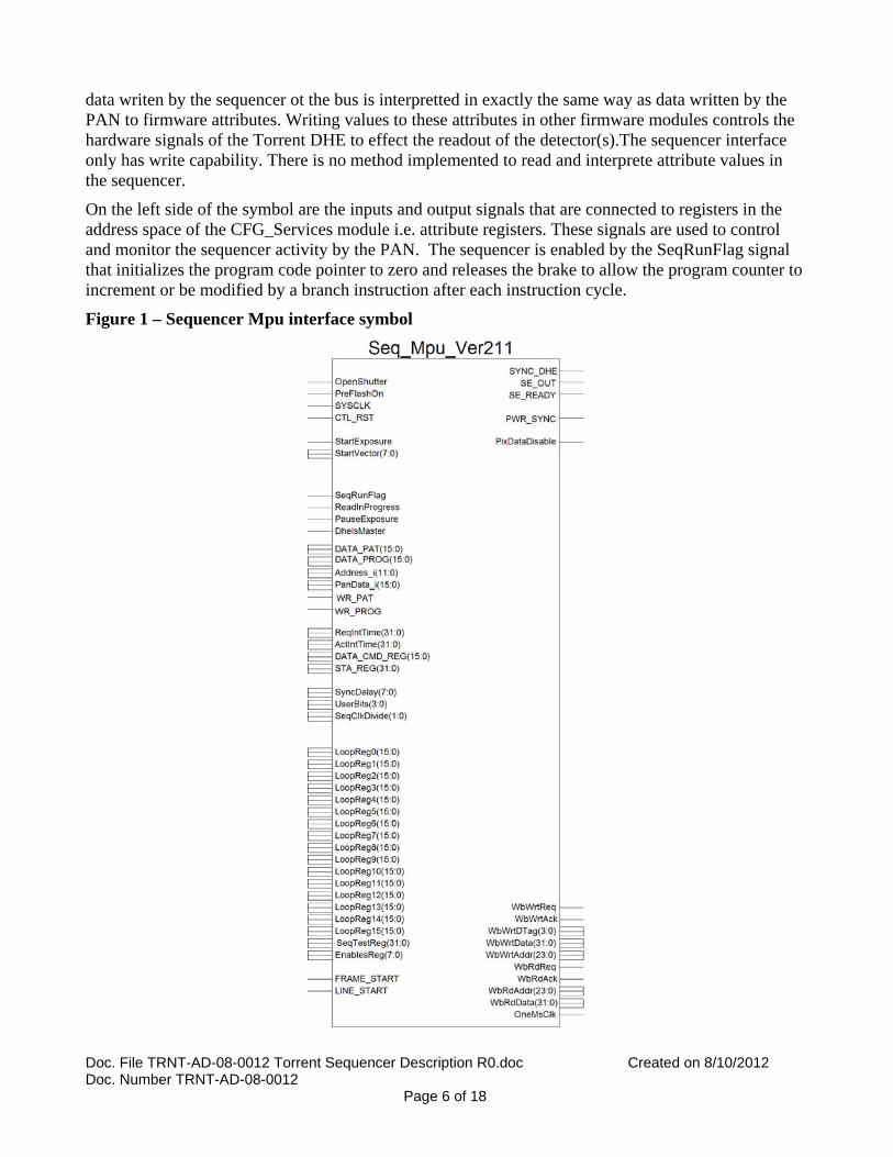
Sequencer Interface The simplified sequencer interface symbol is shown in Figure 1. The sequencer is incorporated into the Configuration Services firmware module (CFG_Services). On the lower right side of the symbol are the Wishbone bus master interface signals that allows the Mpu to write to the Torrent firmware bus structure. The Wishbone bus is used to communicate between the different firmware function modules that control the Torrent DHE hardware. The Mpu master bus interface is one of two masters in the firmware design (the other is the LCB Control module). The two master interfaces compete for access to the bus through a scheme that maximizes the priority for the sequencer bus interface. The
Doc. File TRNT-AD-08-0012 Torrent Sequencer Description R0.doc Created on 8/10/2012 Doc. Number TRNT-AD-08-0012
Page 6 of 18
data writen by the sequencer ot the bus is interpretted in exactly the same way as data written by the PAN to firmware attributes. Writing values to these attributes in other firmware modules controls the hardware signals of the Torrent DHE to effect the readout of the detector(s).The sequencer interface only has write capability. There is no method implemented to read and interprete attribute values in the sequencer.
On the left side of the symbol are the inputs and output signals that are connected to registers in the address space of the CFG_Services module i.e. attribute registers. These signals are used to control and monitor the sequencer activity by the PAN. The sequencer is enabled by the SeqRunFlag signal that initializes the program code pointer to zero and releases the brake to allow the program counter to increment or be modified by a branch instruction after each instruction cycle.
Figure 1 – Sequencer Mpu interface symbol
Doc. File TRNT-AD-08-0012 Torrent Sequencer Description R0.doc Created on 8/10/2012 Doc. Number TRNT-AD-08-0012
Page 7 of 18
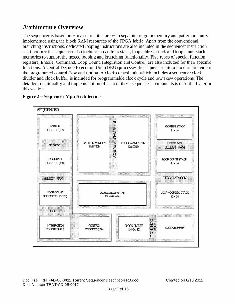
Architecture Overview The sequencer is based on Harvard architecture with separate program memory and pattern memory implemented using the block RAM resources of the FPGA fabric. Apart from the conventional branching instructions, dedicated looping instructions are also included in the sequencer instruction set, therefore the sequencer also includes an address stack, loop address stack and loop count stack memories to support the nested looping and branching functionality. Five types of special function registers, Enable, Command, Loop Count, Integration and Control, are also included for their specific functions. A central Decode Execution Unit (DEU) processes the sequencer micro-code to implement the programmed control flow and timing. A clock control unit, which includes a sequencer clock divider and clock buffer, is included for programmable clock cycle and low skew operations. The detailed functionality and implementation of each of these sequencer components is described later in this section.
Figure 2 – Sequencer Mpu Architecture
Doc. File TRNT-AD-08-0012 Torrent Sequencer Description R0.doc Created on 8/10/2012 Doc. Number TRNT-AD-08-0012
Page 8 of 18
Program Memory The program memory is implemented using the Block RAM resources. The program memory is dual port, 16 bits wide and 1K (1024 words deep, read-write RAM). Both ports are clocked with the same system clock (SysClk). Conventional pipeline-based architecture results in pipeline refill latencies while executing branching instructions that are unacceptable for single clock execution. To avoid such latencies, one port of the program memory is dedicated to substitute for pipelining operation. This is achieved by performing a Program counter + 1 read at the second port of the program memory. Access to this port is limited to the DEU only. Access to the other port of the program memory is multiplexed between the PAN and the sequencer DEU. The PAN is only given authority to access the program memory when the SeqRunFlag signal is false.
The DEU accesses the program memory using an internal program counter register. This register is reset to zero whenever the SeqRunFlag signal goes true and is subsiquently modified by the DEU logic to either point to the next instruction (i.e. increment) or loaded with a new value by a ‘Jump if Control Bit’ branch instruction (JCB).
Pattern Memory The pattern memory is dual port 32K bits of read-write RAM. The two ports of pattern memory include independent read-write PAN port and read only DEU port but differing in width and depth. From the PAN port the program memory is 16 bits wide and 2K words deep whereas from the DEU port it is 32 bits wide and 1K patterns deep. The even and odd addressed 16-bit words correspond to the least and most significant 16-bits of a pattern respectively. The dual port access to the pattern memory is not time multiplexed so both PAN and DEU can randomly access the program memory independently. The pattern memory is clocked using the system clock.
Note that values in the program and pattern memories are volatile and not cleared by a reset operation so they require explicit write commands from the PAN to clear and load the contents of the program and pattern Memory.
The pattern memory is accessed by the pattern pointer register internal to the DEU. Micro-code instructions exist to load a value to the pattern pointer (LPP) and to increment (IPP) or decrement (DPP) its value. The contents of the pattern memory addressed by the pattern pointer is written to the wishbone bus whenever a bus master write command is issued by the sequencer. This occures whenever a load select register (LSR) instruction is executed.
Stacks The Program Address Stack and Loop Begin Address Stack are 12-bit wide by 64 word deep FILO memory spaces to implement the Program Pointer and Loop Begin Address stack respectively.
The Pattern Pointer stack is a 10-bit by 64-word deep FILO memory space used to hold the current pattern pointer value when a sub-routine is called.
The Loop Count Stack is a 16-bit wide and 64 words deep FILO memory to hold the loop register intermediate value when a loop is active but nested.
The Program Address is pushed into the Program Address Stack whenever a sub-routine is called using the CAL instruction. It is popped back to the program counter register at the end of sub-routine
Doc. File TRNT-AD-08-0012 Torrent Sequencer Description R0.doc Created on 8/10/2012 Doc. Number TRNT-AD-08-0012
Page 9 of 18
execution determined by the RET instruction. The value of the current pattern pointer register is also pushed onto the appropriate stack and popped off by the same instructions.
Similarly, to support nested loop instructions, at the beginning of the loop the next program memory address and previous contents of the loop counter are pushed into their respective stacks and the loop counter is loaded with the new count value from the new loop register. After execution of the loop iteration, if the loop counter is greater than zero, it is decremented and program pointer is re-loaded with the loop beginning address stored at the top of the appropriate stack. Otherwise the program pointer is incremented to point to the next instruction and loop count and loop starting address are both popped out from the sequencer stack.
All three stacks are clocked from the system clock. The Stack memories are not available to the PAN and are controlled by directly by the DEU. Stack memory pointers are cleared by the SeqRunFlag going true.
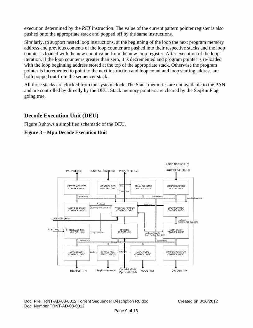
Decode Execution Unit (DEU) Figure 3 shows a simplified schematic of the DEU.
Figure 3 – Mpu Decode Execution Unit
Doc. File TRNT-AD-08-0012 Torrent Sequencer Description R0.doc Created on 8/10/2012 Doc. Number TRNT-AD-08-0012
Page 10 of 18
The decode execution unit is the central control logic of the sequencer. Based on the functionality performed by various instructions, the control logic internal to the Decode execution unit is grouped into various control and data path elements, which collectively perform various functions as briefly explained in sequel.
Program Address Multiplexer As mentioned earlier, the DEU’s access to the program memory Multiplexed Port is time-shared with the PAN Local address. The Program Address Multiplexer implements this priority multiplexed port. Program Counter Control Logic Increments the program counter by the size of the instruction executed (in units nibble) while performing sequential (non-branching) instructions. For branching and sub routine call instructions the counter is loaded with the address specified by the operands. While executing subroutine return and looping instructions, the program counter is loaded with address on the top of the program pointer address stack and loop begin address stack respectively. Apart from this program counter output, another output equal to “Program Counter + 1” is also provided to address the program memory Pipeline Port. Instruction Multiplexer The current instruction set implementation supports a variable instruction size from 1 to a maximum of 5 nibbles or 20 bits. So the maximum size instruction consists of 1 nibble opcode and 4 nibbles operand. The 32-bit data read per clock cycle from the two ports of the Program memory includes 16 bit data at the current memory location addressed by the program counter and the next 16 bits located at the next memory location. The opcode can be the first, second, third or fourth significant nibble of the 16-bit multiplexed port program word if the value of the least significant 2-bits of the program counter is b’00, b’01, b’10 or b’11 respectively. The operand for the maximum size instruction is the following 4 nibbles. Therefore, from the 32 bits program memory data, the Instruction Multiplexer selects a 20-bit valid instruction based on the least significant 2 bits of the program counter at the beginning of every execution cycle. Pattern Pointer Control Logic Logic initializes the pattern pointer to 0 when Reset is asserted. Decodes and executes LPP, IPP and DPP instructions when the sequencer run flag is asserted. Output Registers and Control Logic Apart from the pattern pointer sequencer include three other static registers, namely Select Register, Device Address Register and Output Register to control the sequencer bus. The control logic decodes and executes the LSR, LMR and LDA instructions to load the operand data into Select registers, Mode register and Device Address register on respective execution. Program Counter Stack Control Logic Decodes sub-routine Call and Return instruction and performs Stack Memory push (write) and pop (read) operations respectively.
Doc. File TRNT-AD-08-0012 Torrent Sequencer Description R0.doc Created on 8/10/2012 Doc. Number TRNT-AD-08-0012
Page 11 of 18
Loop Control Logic Controls the Loop Counter and selects the addressed Loop Register from the bank of 16 loop registers using an internal Loop register Multiplexer while executing looping instructions. Also controls the push and pop operations on Loop Count Stack and Loop Begin Address Stack for implementing nested loop functionality. EFR Write Decode Asserts a write to the enables register when local select bit in the select register is asserted and the pattern of the mode register bits correspond to the write mode. Delay Control Logic Three delay counters, clock-counter, microsecond counter and millisecond counter are designed to insert the explicitly specified blocking timing delays apart from the non-blocking integration time controller. The delay control logic decodes the delay instruction and loads the corresponding resolution down counter with specified value in the operands. Once the counters are loaded, they start decrementing to implement the specified delay and block the sequencer from executing the next instruction until all counters are reduced to inactive zero state. On reset, all three counters are initialized to zero value.
Special Function Registers The sequencer includes the following special function registers that are used to control the function and determine the status of the sequencer Mpu:
Sequencer Run Enable register (SeqEnable attribute) This is a single bit register that when set true resets the program and stack pointer regsietsr and allows the program counter to be incremented. Note that the first instruction at program memory address zero in the micro-code should be a NOP instruction to allow the instruction pipeline to fill up. This is a firmware feature.
DHE is a Slave register (DheIsSlave attribute) This 1-bit regsietr designates the Torrent DHE as a slave device when set true. This has significance to on how the synchronization logic is used to either wait for a synchronization signal (when slaved) or to generate a synchronization signal (when set as a master DHE). When this attribute is set true the DHE looks for and acquires an external hardware clock source.
Command register (SeqCmds attribute) This register is a combination of hardwired and software settable flags. The intended purpose is to provide a conditional jump capability within the sequencer micro code by using the sequencer instruction “Jump if Control Bit Set” (JCB). This instruction allows any of the 16 flags to be tested for an active condition.
Bit 0: Unconditional Jump. Always tied to '1' to facilitate the implementation of unconditional jump. Default 1 Active 1. Bit 1: SYNC_IN This bit reflects the condition of the SYNC_DHE input signal when the Torrent DHE is configured for slave mode operation. In Master mode this bit reflects the status of the
Doc. File TRNT-AD-08-0012 Torrent Sequencer Description R0.doc Created on 8/10/2012 Doc. Number TRNT-AD-08-0012
Page 12 of 18
SYNC_DHE output controlled by the Enable Function Register (EFR) and sync logic. Default 0 Active 1. Bit 2: Integration Timer Terminal Count This bit is set when the Integration Time counter (ITC) reaches a value greater or equal to that stored in the Integration Time register (IntegrationTime attribute). The flag will remain set until either the Integration Time register is loaded with a larger value than the ITC contents or the enable bit in the EFR register re-activates the integration timer. Default condition (after reset) is active since the ITC and the RIT are reset to zero. If this bit is to be used to determine if the integration timer is active, the PAUSE bit in the control register should also be checked. Default 1 Active 1. Bit 3: Start Exposure Active High. This bit is set when the DHE receives a “Start Exposure” command from the PAN. It remains set until a reset start exposure flag bit is set via the EFR. The purpose of this bit is to act as a qualifier for bits 4 to 11 of this register. Default 0 Active 1. Bit 4 to Bit 11: Start Exposure vector. These bits are latched from the address portion of the start exposure command at the same time as bit 3. They are meant to enable a variety of sequence actions to be selected based upon the bits set and the use of the JCB instruction in the sequencer micro code to test their condition. Default 0 Active 1. Bit 12 to Bit 15: User Defined Bit Pattern. These bits are written directly to the command register from the PAN by writing to the User Control Bits register (SeqUserBits attribute). They are transposed from bits 0 to 3 in the data written to this attribute. Default 0 Active 1.
Integration Time register (IntegrationTime attribute) The Integration Time Register is 32-bit wide and has a resolution of 1ms. This register is programmed by the PAN with the required detector integration. The integration period delay is implemented using an internal up counter called the ‘Integration Timer Counter’ (ITC). When the ITC is enabled by the the appropriate bit of the EFRegister by a sequencer write instruction to the EFR, the internal ITC counter is reset to zero and begins counting up each millisecond until a value equal to the value loaded into the Integration Time register is equaled or exceeded. When this condition is met the ‘Terminal Count’ (TC) flag in the command register is set true. The ITC register continues to increment until the appropriate EFR enable bit is reset by the sequencer. The ITC register is cleared when the ITC enable bit goes true at the beginning of an integration period. The ITC is inhibited from incrementing by the PauseExposure attribute register being set true.
Doc. File TRNT-AD-08-0012 Torrent Sequencer Description R0.doc Created on 8/10/2012 Doc. Number TRNT-AD-08-0012
Page 13 of 18
Pause the Exposure register (PauseExposure attribute) Setting this 1-bit attribute true will stop the Integration Time Counter (ITC) from incrementing. This action also forces the shutter and preflash signals false if they were set. Resetting this bit will allow the ITC to continue counting up and restores the prior condition of the shutter and preflash signals. Default 0 Active 1.
Synchronize Command Delay register (SyncDelay attribute) When acting as a master DHE, there is a finite time that is needed to assure that each slave DHE has received the ‘start exposure command’ before the master issues the synchronization pulse sequence. This register is used to program the the delay time for the master DHE to wait before initiating a synchronization sequence to the slaves.
User Control Bits register (SeqUserBits attribute) This 4-bit register is used by the PAN to write to the Command register bits 15:12 (SeqCmds attribute). These bits are testable by the JCB instruction to determine modes of operation by the sequencer (e.g. ROI readout, continous clear, etc.)
Sequencer Clock Divider register (SeqClkDivide attribute) This 2-bit attribute defines the sequencer clock frequency and hence the instruction time for the sequencer. Note that the current maximum frequency is half the system clock frequency. Each micro code instruction takes one sequencer clock cycle to complete.
00 – SeqClk = SysClk / 2 = 37ns = 26.5625 MHz
01 – SeqClk = SysClk / 4 = 75ns = 13.28125 MHz
10 – SeqClk = SysClk / 8 = 150ns = 6.640625 MHz
11 – SeqClk = SysClk / 16 = 300ns = 3.320125 MHz
Default 00.
Sequencer Status register (SeqStatus attribute) This is a read only attribute that returns the run status, the wishbone request signal status, and the current program counter and stack pointer values. It is of limited operational use and mainly used for diagnosing problems with the sequencer micro-code.
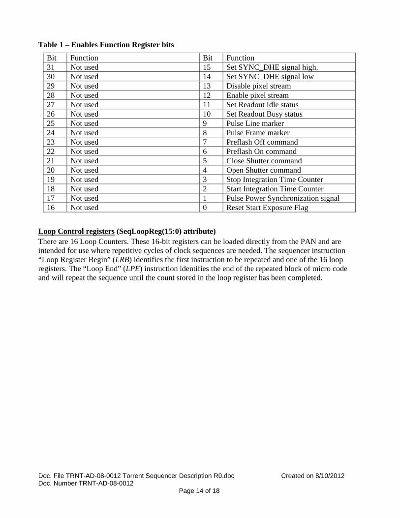
Enable Flag register (SeqEFR attribute) The EFR is a read only attribute from the point of view of the PAN. It is writable by the sequencer Mpu and used to set the state of certain hardware functions specific to the sequencer. The EFR register outputs control signals. These control signals are set or reset by the sequencer executing a write instruction to the address of the internal EFR register at address 0x0108 of the CFG_Services module with the appropriate bit(s) set in the value of the pattern memory pointed to by the pattern memory pointer. This value is written to the EFR register to set or reset bits with the following significance:
Doc. File TRNT-AD-08-0012 Torrent Sequencer Description R0.doc Created on 8/10/2012 Doc. Number TRNT-AD-08-0012
Page 14 of 18
Table 1 – Enables Function Register bits
Bit Function Bit Function 31 Not used 15 Set SYNC_DHE signal high. 30 Not used 14 Set SYNC_DHE signal low 29 Not used 13 Disable pixel stream 28 Not used 12 Enable pixel stream 27 Not used 11 Set Readout Idle status 26 Not used 10 Set Readout Busy status 25 Not used 9 Pulse Line marker 24 Not used 8 Pulse Frame marker 23 Not used 7 Preflash Off command 22 Not used 6 Preflash On command 21 Not used 5 Close Shutter command 20 Not used 4 Open Shutter command 19 Not used 3 Stop Integration Time Counter 18 Not used 2 Start Integration Time Counter 17 Not used 1 Pulse Power Synchronization signal 16 Not used 0 Reset Start Exposure Flag
Loop Control registers (SeqLoopReg(15:0) attribute) There are 16 Loop Counters. These 16-bit registers can be loaded directly from the PAN and are intended for use where repetitive cycles of clock sequences are needed. The sequencer instruction “Loop Register Begin” (LRB) identifies the first instruction to be repeated and one of the 16 loop registers. The “Loop End” (LPE) instruction identifies the end of the repeated block of micro code and will repeat the sequence until the count stored in the loop register has been completed.
Doc. File TRNT-AD-08-0012 Torrent Sequencer Description R0.doc Created on 8/10/2012 Doc. Number TRNT-AD-08-0012
Page 15 of 18
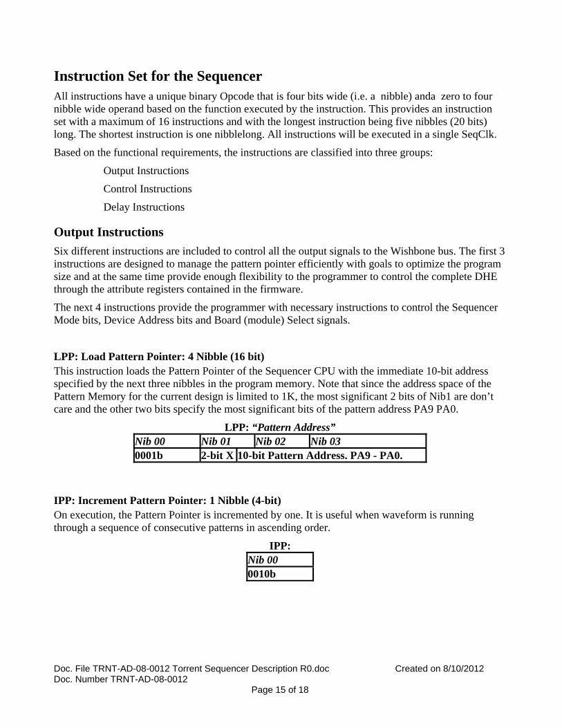
Instruction Set for the Sequencer All instructions have a unique binary Opcode that is four bits wide (i.e. a nibble) anda zero to four nibble wide operand based on the function executed by the instruction. This provides an instruction set with a maximum of 16 instructions and with the longest instruction being five nibbles (20 bits) long. The shortest instruction is one nibblelong. All instructions will be executed in a single SeqClk.
Based on the functional requirements, the instructions are classified into three groups:
Output Instructions
Control Instructions
Delay Instructions
Output Instructions Six different instructions are included to control all the output signals to the Wishbone bus. The first 3 instructions are designed to manage the pattern pointer efficiently with goals to optimize the program size and at the same time provide enough flexibility to the programmer to control the complete DHE through the attribute registers contained in the firmware.
The next 4 instructions provide the programmer with necessary instructions to control the Sequencer Mode bits, Device Address bits and Board (module) Select signals.
LPP: Load Pattern Pointer: 4 Nibble (16 bit) This instruction loads the Pattern Pointer of the Sequencer CPU with the immediate 10-bit address specified by the next three nibbles in the program memory. Note that since the address space of the Pattern Memory for the current design is limited to 1K, the most significant 2 bits of Nib1 are don’t care and the other two bits specify the most significant bits of the pattern address PA9 PA0.
LPP: “Pattern Address” Nib 00 Nib 01 Nib 02 Nib 03 0001b 2-bit X 10-bit Pattern Address. PA9 - PA0.
IPP: Increment Pattern Pointer: 1 Nibble (4-bit) On execution, the Pattern Pointer is incremented by one. It is useful when waveform is running through a sequence of consecutive patterns in ascending order.
IPP: Nib 00 0010b
Doc. File TRNT-AD-08-0012 Torrent Sequencer Description R0.doc Created on 8/10/2012 Doc. Number TRNT-AD-08-0012
Page 16 of 18
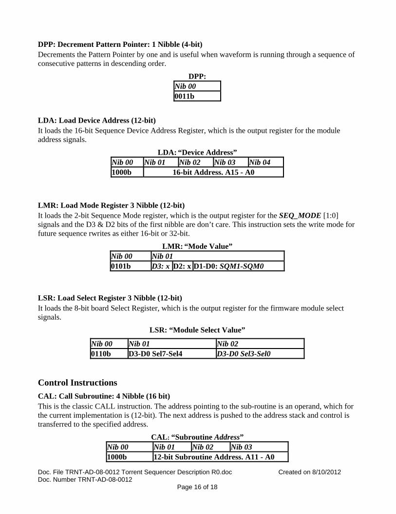
DPP: Decrement Pattern Pointer: 1 Nibble (4-bit) Decrements the Pattern Pointer by one and is useful when waveform is running through a sequence of consecutive patterns in descending order.
DPP: Nib 00 0011b
LDA: Load Device Address (12-bit) It loads the 16-bit Sequence Device Address Register, which is the output register for the module address signals.
LDA: “Device Address” Nib 00 Nib 01 Nib 02 Nib 03 Nib 04 1000b 16-bit Address. A15 - A0
LMR: Load Mode Register 3 Nibble (12-bit) It loads the 2-bit Sequence Mode register, which is the output register for the SEQ_MODE [1:0] signals and the D3 & D2 bits of the first nibble are don’t care. This instruction sets the write mode for future sequence rwrites as either 16-bit or 32-bit.
LMR: “Mode Value” Nib 00 Nib 01 0101b D3: x D2: x D1-D0: SQM1-SQM0
LSR: Load Select Register 3 Nibble (12-bit) It loads the 8-bit board Select Register, which is the output register for the firmware module select signals.
LSR: “Module Select Value”
Nib 00 Nib 01 Nib 02 0110b D3-D0 Sel7-Sel4 D3-D0 Sel3-Sel0
Control Instructions CAL: Call Subroutine: 4 Nibble (16 bit) This is the classic CALL instruction. The address pointing to the sub-routine is an operand, which for the current implementation is (12-bit). The next address is pushed to the address stack and control is transferred to the specified address.
CAL: “Subroutine Address” Nib 00 Nib 01 Nib 02 Nib 03 1000b 12-bit Subroutine Address. A11 - A0
Doc. File TRNT-AD-08-0012 Torrent Sequencer Description R0.doc Created on 8/10/2012 Doc. Number TRNT-AD-08-0012
Page 17 of 18
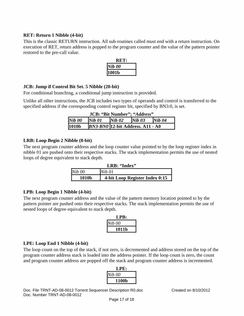
RET: Return 1 Nibble (4-bit) This is the classic RETURN instruction. All sub-routines called must end with a return instruction. On execution of RET, return address is popped to the program counter and the value of the pattern pointer restored to the pre-call value.
RET: Nib 00 1001b
JCB: Jump if Control Bit Set. 5 Nibble (20-bit) For conditional branching, a conditional jump instruction is provided.
Unlike all other instructions, the JCB includes two types of operands and control is transferred to the specified address if the corresponding control register bit, specified by BN3:0, is set.
JCB: “Bit Number”; “Address” Nib 00 Nib 01 Nib 02 Nib 03 Nib 04 1010b BN3-BN0 12-bit Address. A11 - A0
LRB: Loop Begin 2 Nibble (8-bit) The next program counter address and the loop counter value pointed to by the loop register index in nibble 01 are pushed onto their respective stacks. The stack implementation permits the use of nested loops of degree equivalent to stack depth.
LRB: “Index” Nib 00 Nib 01
1010b 4-bit Loop Register Index 0:15
LPB: Loop Begin 1 Nibble (4-bit) The next program counter address and the value of the pattern memory location pointed to by the pattern pointer are pushed onto their respective stacks. The stack implementation permits the use of nested loops of degree equivalent to stack depth.
LPB: Nib 00
1011b
LPE: Loop End 1 Nibble (4-bit) The loop count on the top of the stack, if not zero, is decremented and address stored on the top of the program counter address stack is loaded into the address pointer. If the loop count is zero, the count and program counter address are popped off the stack and program counter address is incremented.
LPE: Nib 00
1100b
Doc. File TRNT-AD-08-0012 Torrent Sequencer Description R0.doc Created on 8/10/2012 Doc. Number TRNT-AD-08-0012
Page 18 of 18
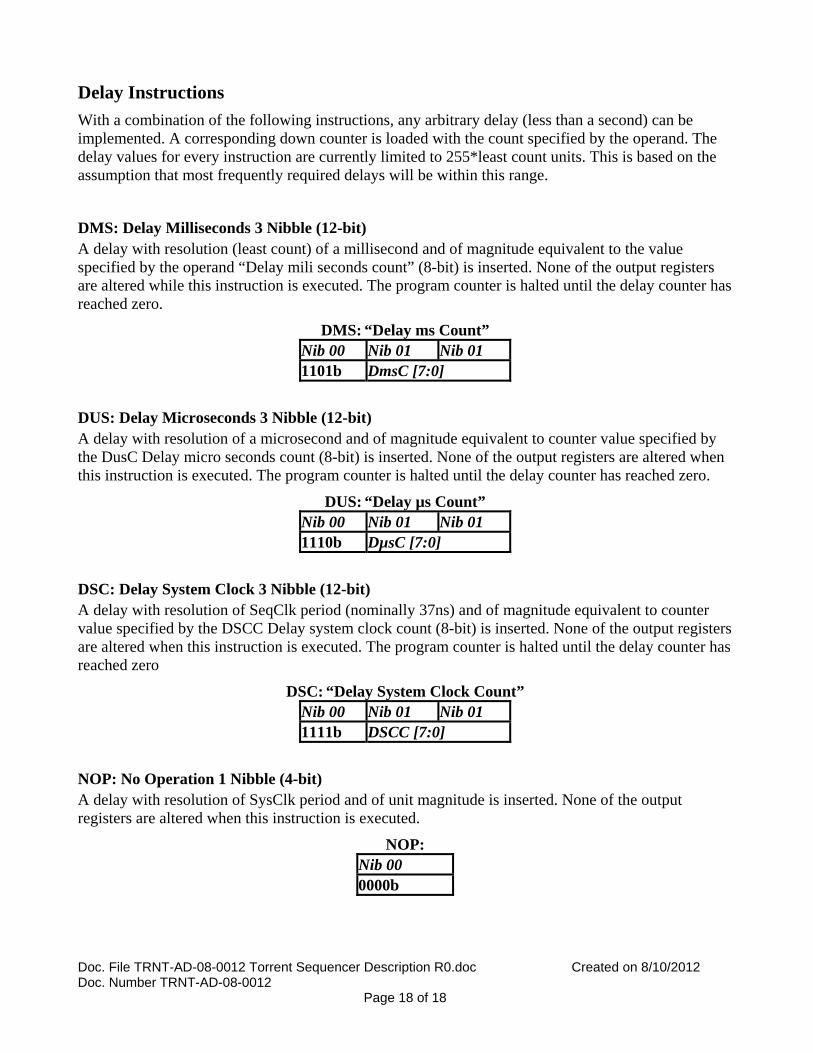
Delay Instructions With a combination of the following instructions, any arbitrary delay (less than a second) can be implemented. A corresponding down counter is loaded with the count specified by the operand. The delay values for every instruction are currently limited to 255*least count units. This is based on the assumption that most frequently required delays will be within this range.
DMS: Delay Milliseconds 3 Nibble (12-bit) A delay with resolution (least count) of a millisecond and of magnitude equivalent to the value specified by the operand “Delay mili seconds count” (8-bit) is inserted. None of the output registers are altered while this instruction is executed. The program counter is halted until the delay counter has reached zero.
DMS: “Delay ms Count” Nib 00 Nib 01 Nib 01 1101b DmsC [7:0]
DUS: Delay Microseconds 3 Nibble (12-bit) A delay with resolution of a microsecond and of magnitude equivalent to counter value specified by the DusC Delay micro seconds count (8-bit) is inserted. None of the output registers are altered when this instruction is executed. The program counter is halted until the delay counter has reached zero.
DUS: “Delay µs Count” Nib 00 Nib 01 Nib 01 1110b DµsC [7:0]
DSC: Delay System Clock 3 Nibble (12-bit) A delay with resolution of SeqClk period (nominally 37ns) and of magnitude equivalent to counter value specified by the DSCC Delay system clock count (8-bit) is inserted. None of the output registers are altered when this instruction is executed. The program counter is halted until the delay counter has reached zero
DSC: “Delay System Clock Count” Nib 00 Nib 01 Nib 01 1111b DSCC [7:0]
NOP: No Operation 1 Nibble (4-bit) A delay with resolution of SysClk period and of unit magnitude is inserted. None of the output registers are altered when this instruction is executed.
NOP: Nib 00 0000b