Embed Size (px)
Citation preview
Datasheet V1.0 | 01.2007 Page 1 of 36
TopSecTM ID Module B.3fingerMetricaMB fingerMetricaMB
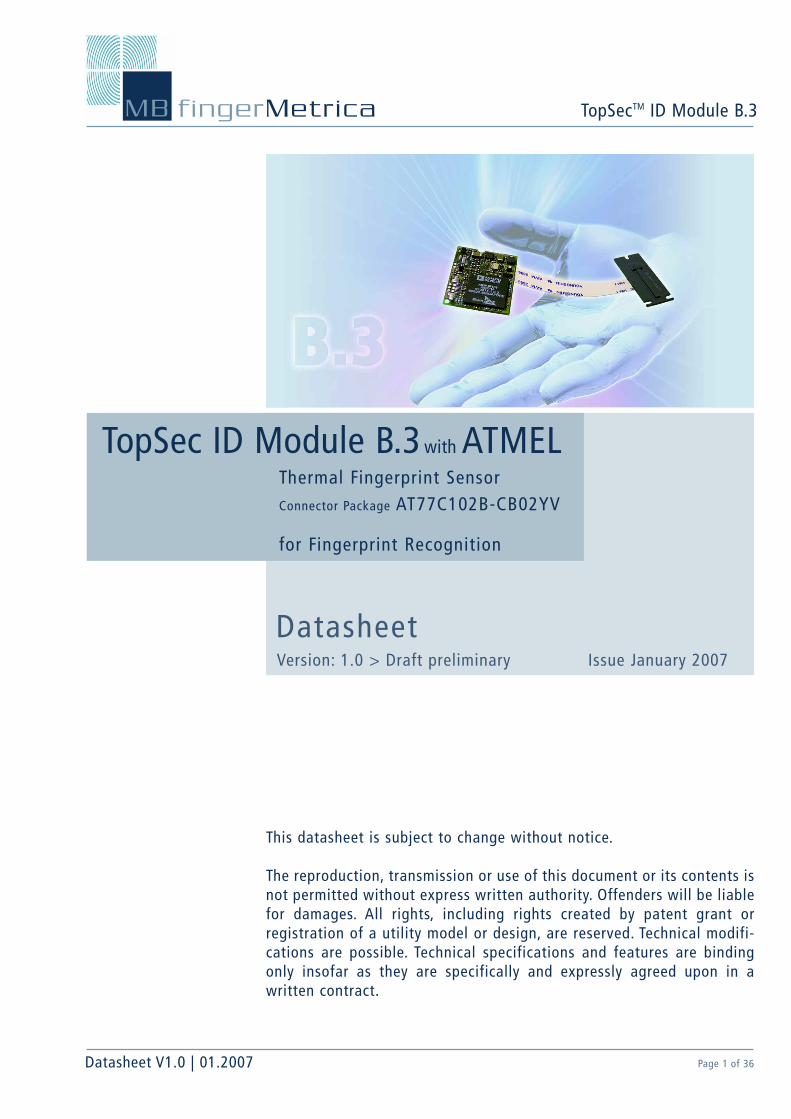
DatasheetIssue January 2007Version: 1.0 > Draft preliminary
TopSec ID Module B.3 with ATMELThermal Fingerprint SensorConnector Package AT77C102B-CB02YV
for Fingerprint Recognition
This datasheet is subject to change without notice.
The reproduction, transmission or use of this document or its contents isnot permitted without express written authority. Offenders will be liablefor damages. All rights, including rights created by patent grant orregistration of a utility model or design, are reserved. Technical modifi-cations are possible. Technical specifications and features are bindingonly insofar as they are specifically and expressly agreed upon in awritten contract.
TopSecTM ID Module B.3fingerMetricaMB
Datasheet V1.0 | 01.2007 Page 2 of 36
Important – For further information please contact:
Published by MB fingerMetrica GmbHBgm.-Templer-Ring 9, 86703 Rögling
© Copyright MB fingerMetrica GmbH, All Rights reserved
TopSecTM is a registered trademark of Siemens AG / MB fingerMetrica GmbH
FingerChipTM is a registered trademark of ATMEL
Blackfin is a registered trademark of Analog Devices
Phone: +49-(0) 90 94-9 21 02 98Fax: +49-(0) 90 94-9 21 02 99
E-Mail: [email protected]: www.mbfingermetrica.com
MB fingerMetrica GmbHEmbedded fingerprint applications
Bürgermeister-Templer-Ring 986703 Rögling | Germany

TopSecTM ID Module B.3fingerMetricaMB
Datasheet V1.0 | 01.2007 Page 3 of 36
Contents:
List of Figures and Tables 051. History 06
1.1. References 061.2. Glossary 071.3. Abbreviations 071.4. General Introduction 08
2. Overview 092.1. Add-on’s 102.2. Features, Position in the System 102.3. Functional block diagram of TopSec ID Module B.3 12
3. Interfaces 133.1. Host Interface 13
3.1.1. General Description 133.1.2. Connector 143.1.3. Power Supply 163.1.4. UART0 – Interface 173.1.5. UART1 – Interface 173.1.6. I2C – Interface 173.1.7. SPI – Interface 183.1.8. CAN – Interface 183.1.9. Bootmode Selection 183.1.10. General GPIO Lines 183.1.11. Electrical Characteristics 19
3.2. ATMEL Stripe Sensor Interface 223.2.1. Sensor Malfunction 22
3.3. External RAM/Flash Memory 223.4. ESD 223.5. Direct User Interface 243.6. Power Management 24
3.6.1. OFF State – Shut Down 243.6.2. IDLE State – Hibernate 243.6.3. ACTIVE State 25
3.7. Reset 253.8. Application Examples 25
3.8.1. Host Controlled Mode – Single Host System 253.8.2. Host Controlled Mode – Double Host System 26
3.8.2.1. Interface RS232/RS485/RS422 263.8.3. Autonomous Mode 273.8.4. Multiple Module Access by Single Host 27

TopSecTM ID Module B.3fingerMetricaMB
Datasheet V1.0 | 01.2007 Page 4 of 36
3.9. Mechanical Dimensions 283.9.1. TopSec ID Module B.3 283.9.2. Position of Flexible PCB Interconnect 293.9.3. ATMEL FingerChipTM Sensor 293.9.4. ATMEL FingerChipTM Module Assembly 303.9.5. Checklist for a ATMEL FingerChipTM Module Assembly 303.9.6. Alignment and Fixing of the ATMEL FingerChipTM in a System 31
3.10. Environmental Qualification 323.10.1. Climate Qualification 323.10.2. Mechanical Qualification 333.10.3. EMC-/ESD-Qualification 333.10.4. Corrosive Gas Atmosphere 343.10.5. Sensor Sunlight Resistance 343.10.6. Sensor Chemical Resistance 343.10.7. Sensor Abrasive Resistance / Simulated Finger Touch Test 353.10.8. Sensor Scratch Resistance / Impact Resistance 353.10.9. Product Safety 353.10.10. Environmental Compatibility 353.10.11. Standards, Approvals, Markings 353.10.12. Notes on EMC/ESD 35
3.11. Reliability 36
TopSecTM ID Module B.3fingerMetricaMB
Datasheet V1.0 | 01.2007 Page 5 of 36
List of Figures and Tables:
Figure 1: Module identifier 09Figure 2: TopSec ID Module B.3 10Figure 3: Block diagram 12Figure 4: ESD – Protection ground 23Figure 5: Application example 1 for host controlled mode 25Figure 6: Application example 2 for host controlled mode 26Figure 7: Interface circuits 26Figure 8: Unsupported bus interface interconnect 27Figure 9: Discrete interface interconnect 27Figure 10: Mechanical dimensions of TopSecTM ID Module B.3 28Figure 11: Position of the flexprint connection 29Figure 12: B.3 with ATMEL Thermal Fingerprint Sensor (both backside) 29Figure 13: Product Package 29Figure 14: System design for ATMEL FingerChipTM 30
Table 1: History 06Table 2: Module identifier 09Table 3: Host interface connector 14/15Table 4: Host interface: Absolute maximum ratings 19Table 5: Host interface: Recommended operating conditions 20Table 6: Host interface: DC electrical characteristics 21Table 7: Climate qualification, operating conditions 32Table 8: Climate qualification, storage and transportation 32Table 9: Mechanical qualification 33Table 10: Radiated emission 33Table 11: Radiated immunity 33Table 12: Electrostatic discharge 34Table 13: Corrosive gas atmosphere 34Table 14: Blocking 36
TopSecTM ID Module B.3fingerMetricaMB
Datasheet V1.0 | 01.2007 Page 6 of 36
1. History
Version Date Changes1.0 2006–12–30 first issue
Table 1: History
Important changes to the previous version are marked with a vertical line on the left side.
1.1. References
/1.1/ TopSec ID Module A1 Data Sheet V1.10 (01/01)
/2.1/ ID Module Interface Description; actual Version
/3.1/ TopSec ID Module SDK – Operating and Installations Instructions V1.1
/4.1/ ATMEL AT77C102B FingerChipTM. Databook Rev. 5364A-BIOM-09/05Sensor Version AT77C102B - CB02YV, Flex Print Connector
/4.2/ ATMEL AT77C104B - CB0BYV Fingerprint Sensor Qualification Plan

TopSecTM ID Module B.3fingerMetricaMB
Datasheet V1.0 | 01.2007 Page 7 of 36
1.2. Glossaryuser this term means the one, who assembles the module into the final device (OEM)end user this term means the one, who uses the module in the final device to identify himselfmodule this term is used for the ID Module B.3, specified in this paperFW firmware: is the program permanently stored in the Flash-EPROM of the module;
permanently means that it is not volatile under normal operating conditions, but it can be reprogrammed (updated) through the host interface
1.3. Abbreviations#-postfix indicates active low signalsACI Asynchronous Communication InterfaceCE Communautés Européennes (conformity mark of the European Union)CMOS Complementary Metal Oxide SemiconductorCSA Canadian Standards AssociationC-UL Canadian version of ULEMC Electromagnetic CompatibilityEMI Electromagnetic InfluenceEN Europäische Norm (European Standard)EPP Enhanced Parallel PortESD Electrostatic DischargeFCC Federal Communications CommissionFFC Flat Flexible CircuitryFPC Flat Printed CableFW FirmwareGND GroundHW HardwareIC Integrated CircuitLDO Low Dropout (Regulator)LED Light Emitting DiodeNC Not ConnectedOEM Original Equipment ManufacturerPC Personal ComputerPG Protection GroundSDK Software Development KitSW Software

TopSecTM ID Module B.3fingerMetricaMB
Datasheet V1.0 | 01.2007 Page 8 of 36
1.4. General Introduction1) This document describes the hardware features, technical design in requirements and qualification of the
TopSec ID Module B.3 together with connected ATMEL stripe sensor.
2) MB fingerMetrica GmbH substitutes its current product “TopSec ID module/Infineon sensor” with thisnew hardware platform.
3) This HW design guarantees to manufacture and deliver a cheap and highly qualified (reliability) embeddedmodule, which can be upgraded with different firmware functionalities through the end users and integra-tors using FW upgrade service tool functions.
4) The known biometric firmware functions and all other firmware functions of the current TopSec IDModule A1 run on the TopSec ID Module B.3.
5) The TopSec ID Module B.3 and its connected ATMEL sensor are fully ROHS compliant according to theEuropean Directive for Restriction of Hazardous Substances (RoHS).
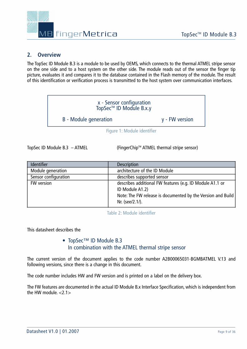
2. OverviewThe TopSec ID Module B.3 is a module to be used by OEMS, which connects to the thermal ATMEL stripe sensoron the one side and to a host system on the other side. The module reads out of the sensor the finger tippicture, evaluates it and compares it to the database contained in the Flash memory of the module. The resultof this identification or verification process is transmitted to the host system over communication interfaces.
x - Sensor configurationTopSecTM ID Module B.x.y
B - Module generation y - FW version
Figure 1: Module identifier
TopSec ID Module B.3 – ATMEL (FingerChipTM ATMEL thermal stripe sensor)
Identifier DescriptionModule generation architecture of the ID ModuleSensor configuration describes supported sensorFW version describes additional FW features (e.g. ID Module A1.1 or
ID Module A1.2)Note: The FW release is documented by the Version and Build Nr. (see/2.1/).
Table 2: Module identifier
This datasheet describes the
• TopSec™ ID Module B.3 In combination with the ATMEL thermal stripe sensor
The current version of the document applies to the code number A2B00065031-BGMBATMEL V.13 andfollowing versions, since there is a change in this document.
The code number includes HW and FW version and is printed on a label on the delivery box.
The FW features are documented in the actual ID Module B.x Interface Specification, which is independent fromthe HW module. <2.1>
TopSecTM ID Module B.3fingerMetricaMB
Datasheet V1.0 | 01.2007 Page 9 of 36
TopSecTM ID Module B.3fingerMetricaMB
Datasheet V1.0 | 01.2007 Page 10 of 36
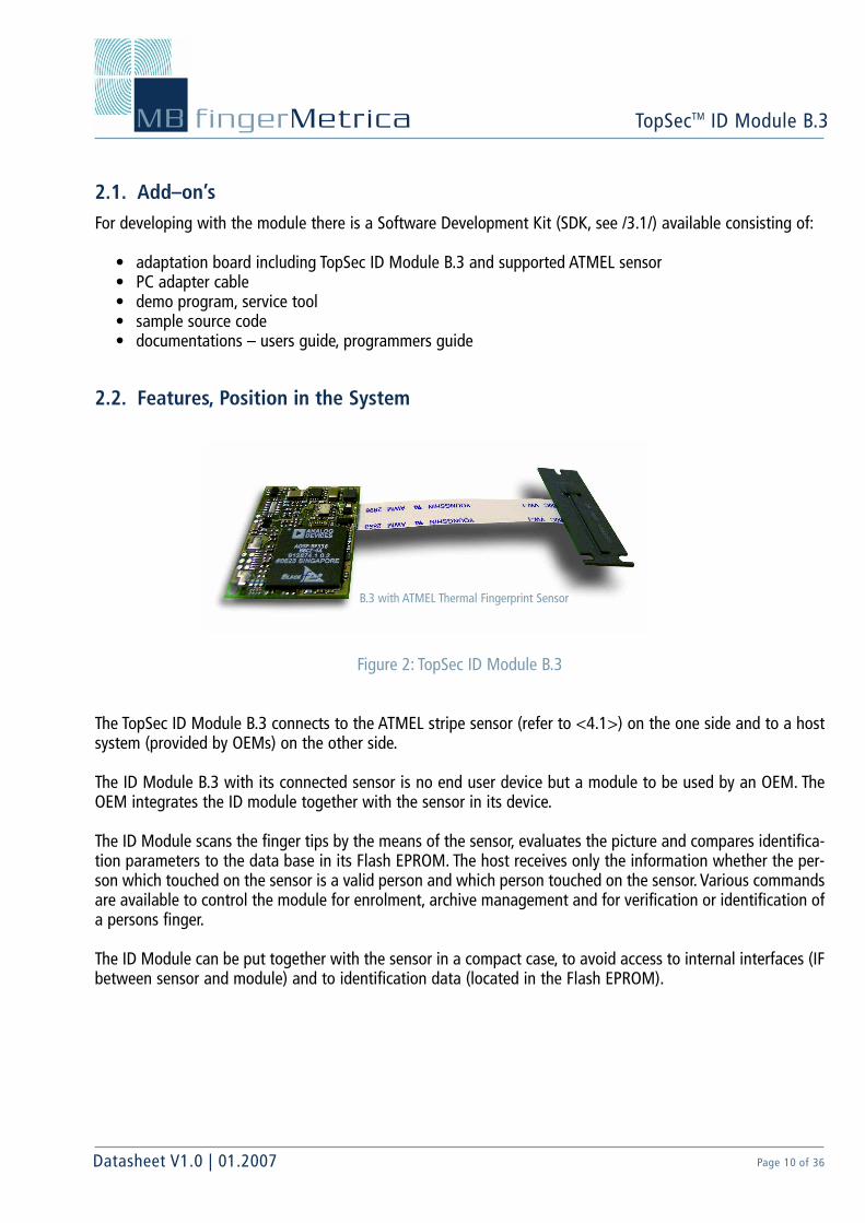
B.3 with ATMEL Thermal Fingerprint Sensor
2.1. Add–on’sFor developing with the module there is a Software Development Kit (SDK, see /3.1/) available consisting of:
• adaptation board including TopSec ID Module B.3 and supported ATMEL sensor• PC adapter cable• demo program, service tool• sample source code• documentations – users guide, programmers guide
2.2. Features, Position in the System
Figure 2: TopSec ID Module B.3
The TopSec ID Module B.3 connects to the ATMEL stripe sensor (refer to <4.1>) on the one side and to a hostsystem (provided by OEMs) on the other side.
The ID Module B.3 with its connected sensor is no end user device but a module to be used by an OEM. TheOEM integrates the ID module together with the sensor in its device.
The ID Module scans the finger tips by the means of the sensor, evaluates the picture and compares identifica-tion parameters to the data base in its Flash EPROM. The host receives only the information whether the per-son which touched on the sensor is a valid person and which person touched on the sensor. Various commandsare available to control the module for enrolment, archive management and for verification or identification ofa persons finger.
The ID Module can be put together with the sensor in a compact case, to avoid access to internal interfaces (IFbetween sensor and module) and to identification data (located in the Flash EPROM).

TopSecTM ID Module B.3fingerMetricaMB
Datasheet V1.0 | 01.2007 Page 11 of 36
The ID Module currently supports two serial communication interfaces:
UART1 Asynchronous serial communication interface (TTL levels) for host communicationUART0 Maintenance Interface (TTL levels, RS232 conversion must be done externally) for an
asynchronous computer communicaton, e.g. for downloading a new FW from a PC to theID Module or for user enrolment.
For easing the communication between host and module indication lines to the host and interrupt input to themodule can be provided by using of available GPIO lines.
Power has to be supplied externally (host system or battery). To reduce power consumption different operatio-nal modes are implemented (see chapter 3.6).
For certain purposes, several GPIO lines are available which can fulfil the indication-, interrupt-, and key linefunction of the TopSec ID Module A1. There are no onboard LEDs and open collector outputs on the TopSec IDmodule B.3.
The host connector also carries an I2C interface which can be used in a Master or Slave direction.TopSec ID Module B.1 boot mode also can be controlled over the host IF. It is set to default „Boot from Flash“via internal pull down resistors.
In addition the host connector carries a full SPI interface, which can be used in Master or Slave configuration.This interface is used for loading the bootloader/test software during manufacturing and uses the SPI Bootmode protocol (SPI initial boot mode). The complete SPI IF is available at test points. It can be used (option) asa further HOST control IF or as an interface to connect further peripherals (display, keypad, &).

TopSecTM ID Module B.3fingerMetricaMB
Datasheet V1.0 | 01.2007 Page 12 of 36
2.3. Functional block diagram of TopSec ID Module B.3
Figure 3: Block diagram
The module is built around a high-performance digital signal processor ADSP-BF536.Program and enrolment data are stored in a Flash EPROM (3MB).
The inputs at the host interface are connected to the processor through a 5V tolerant buffer, the outputs aredirectly connected to the processor. The UART0 lines are protected against ESD.
All internal power supply voltages for the logic are produced internal on board. With ATMEL sensor usage theTopSec ID module B.3 can be supplied in a wide operating voltage area from 3.3VDC to 6,5VDC. There is also avoltage supervisor on board which generates the reset signals for the processor and the Flash EPROM/RAMcomponents.
There is no watchdog on board. If the ID module doesn’t respond to any command the host has to switch themodule “off” and “on”.
The flash banks are addressed via memory select signals. Per default the highest address area is addressed via pulldown resistors (Boot from Flash). It is recommended to write data which belongs together in the same flash bank.

TopSecTM ID Module B.3fingerMetricaMB
Datasheet V1.0 | 01.2007 Page 13 of 36
The external RAM is 1MB PSRAM.The internal RAM (on Chip memory) is 100 kbytes (KB) and is composed of:
32 KB of instructions SRAM/cache48 KB of instructions SRAM16 KB of data SRAM/cache4 KB of scratch pad SRAM.
The external Flash/RAM is available in one Chip which is ATMEL 32 Mbit Flash + 8 Mbit PSRAM Stacked Memory.The JTAG interface is available via an 8 pin JTAG connector (only for prototyping).The TopSec ID Module B.3 connects to the ATMEL sensor over its parallel port interface (PPI).The module connects to its host environment through a 30 pin flex print connector.Optionally the peripheral interface can be equipped with a 60 pin connector.Two wires for a CAN interface are available for future usage.
3. Interfaces
3.1. Host Interface
3.1.1. General Description
1. The board is equipped with a 30 pin connector with the following signals and interfaces.The 30 pin connector carries 2 UART-, one I2C and one SPI (slave, master) interface. In addition several GPIOlines are available, which also can be used as parallel port. For the 60 pin connector (future use) EthernetMAC, a 16 Bit PPI and an additional serial PORT interface are available.
2. The ATMEL sensor is connected via a 21pin flat flex print cable which fit to the appropriate connectors onboth sides. Length of sensor flexprint cable: typical 50 mm
The TopSec ID Module B.3 works together with the known adaptation board of the current TopSec ID moduleA1 SDK.
The TopSec ID Module A.1 known functions (INDO, IND1, INT, Key0, Key1, ConfRD, OCDRV1/2) are connected toGPIO lines of the processor – function depend on the firmware. INDO can be used to select the TopSec IDModule B.3, when the module is in SPI slave mode. Key1 from version A1 is used as the CAN Transmit line andINT line from version A1 is used as the CAN Receive line (wakeup – it is internally connected with the UART1-Rx line). Key0, IND1 and ConfRD from version A1 are used as common GPIO lines for input or output purposes.
Pin 4 can optionally be used as a manual reset function.
For all details please refer to the pin description of the 30 pin connector and it’s appropriate functions.
TopSecTM ID Module B.3fingerMetricaMB
Datasheet V1.0 | 01.2007 Page 14 of 36
Attention: The connector must not be plugged in or pulled out while the host system is active (under voltage).Additional, it must be taken into consideration that this interface is basically not protected againstESD (see also chapters 3.4. and 3.10.12).
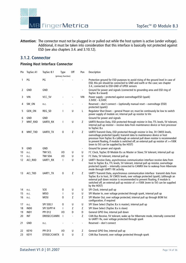
3.1.2. ConnectorPinning Host Interface Connector
Pin TopSec A1 TopSec B.1 Type Off Pon Description(primary function)
1 PG PG - - - Protection ground for ESD purposes to avoid rising of the ground level in case of ESD, this pin should be connected to GND and earth or the case; see chapter 3.4.; connected to ESD-GND of UPEK sensors
2 GND GND - Ground for power and signals (connected to grounding area and ESD ring ofTopSec B.x board)
3 VIN VCC_5V - - VIN Power supply – protected against overvoltage/ESD (spark)3.3VDC - 6,5VDC
4 SW_ON n.c. - - - Reserved – don´t connect – (optionally manual reset – overvoltage (ESD)protected (spark))
5 GEN_ON REG_SD I U L Regulator Shut Down – general Power on; must be continuosly be low to switch power supply of module on; internal pull up resistor to Vin
6 GND GND Ground for power and signals7 MNT_RXD UART0_RX I U Z UART0 Receive Data, ESD protected through resistor in line, TTL levels, 5V tolerant,
internal pull up resistor – receive data from maintenance device or host processor to TopSec B.x
8 MNT_TXD UART0_TX O Z Z UART0 Transmit Data, ESD protected through resistor in line, 3V CMOS levels,overvoltage protected (spark); transmit data to maintenance device or hostprocessor from TopSec B.x (although an external pull down resistor is recommended to prevent floating, if module is switched off, an external pull up resistor of >=100K (even to 5V) can be supplied by the HOST)
9 GND GND - Ground for power and signals10 n.c. TWI SCL I/O U U I2C Clock, TopSec ID Module B.x as Master or Slave; 5V tolerant, internal pull up11 n.c. TWI SDA I/O U U I2C Data, 5V tolerant, internal pull up12 ACI_RXD UART1_RX I U Z UART1 Receive Data, asynchronous communication interface receive data from
host to TopSec B.x, TTL levels, 5V tolerant, internal pull up resistor, overvoltage protected (spark) – internally connected to CANRX line to wakeup from Hibernate mode through UART1 RX activity.
13 ACI_TXD UART1_TX O Z Z UART1 Transmit Data, asynchronous communication interface transmit data from TopSec B.x to host, 3V CMOS levels, over voltage protected (spark); (although an external pull down resistor is recommended to prevent floating, if module isswitched off, an external pull up resistor of >=100K (even to 5V) can be supplied by the HOST)
14 n.c. SCK O U U SPI Clock, internal pull up15 n.c. MISO I U U SPI Master In, over voltage protected through spark, internal pull up16 n.c. MOSI O Z Z SPI Master Out, over voltage protected, internal pull up through BOM list
configuration, if required17 n.c. SPI SSEL1 O U U SPI Slave Select (TopSec B.x is master), internal pull up18 IND0 SPI SS/PF14 I Z Z SPI Slave Select (TopSec B.x is slave)19 IND1 PPI D12 I/O D D General GPIO line, internal pull down20 INT DR0SEC/CANRX I - Z CAN Bus Receive, 5V tolerant, wake up for Hibernate mode, internally connected
to UART1 Rx, over voltage protected through spark21 GND n.c. - - - Reserved – don´t connect
22 KEY0 PPI D13 I/O U Z General GPIO line, internal pull up23 KEY1 DT0SEC/CANTX O U Z CAN Bus Transmit, over voltage protected through spark

TopSecTM ID Module B.3fingerMetricaMB
Datasheet V1.0 | 01.2007 Page 15 of 36
24 CONFRD PPI D11 I/O Z Z General GPIO line25 CONF0 BMODE2 I D D Boot Mode Selection, internal pull down for Boot from Flash as Default26 CONF1 BMODE1 I D D Boot Mode Selection, internal pull down for Boot from Flash as Default;
High forces boot from SPI27 OCDRV0 PPI D10 I/O Z Z General GPIO line
28 OCDRV1 PPI D9 I/O Z Z General GPIO line29 DRVGND n.c. - - - Reserved – don´t connect30 PG Turbo - - - Connected to PG
Table 3: Host interface connectorLegend for Table 3:
> column „typ“: type of pin
I input (from host to module)O output (from module to host)I/O input/output (from module to host or host to module)
> column „off“: state of pins, when module power is turned off> column „pon“: state of pins, between power on reset and FW initialization
L low level (with the appropriate voltage)H high level (with the appropriate voltage)Z high impedanceU weak high through pull up resistorD weak low through pull down resistorI weak low level through chip input diodes (must not be driven in power off!)
General notes on pull up/down resistors:
> All unused input pins can be left open, because they all have internal pull up/down resistors.(exeption: PIN 24, 27, 28)
> REG_SD and PPI D13 have their pull up resistors tied to VIN and can therefore also be driven high.
> UART0_RX and UART1_RX have internal pull up resistors and are decoupled through lateral MOS-transistorsor diodes and can therefore also be driven high.
> It is not recommended to use external pull up resistor at the output pins MNT_TXD, ACI_TXD, UART0_TXand UART1_TX because the module would be (partially) supplied through the pull up resistors, when it isturned off.
> Signal INT and UART1 IF should not be used at the same time.
Please see also chapters 3.4. (ESD) and 3.10.12. (Notes on EMC/ESD).

TopSecTM ID Module B.3fingerMetricaMB
Datasheet V1.0 | 01.2007 Page 16 of 36
3.1.3. Power SupplyPins: VCC_5V .......... power supply
GND .......... ground for power and signalsPG .......... protection groundREG_SD .......... general power on
VCC_5V has to be connected to the power supply (with respect to GND). The module is not protected againstconfusing the poles and has no current limiting.
The host has to provide a power supply with a maximum of 10 V SELV according to IEC 60950 and UL 1950.Also the maximum current has to be limited by the host system, to avoid heating up of the module in case ofmodule failures (see chapter 3.2.1.).
PG is an ESD protection ground line from the sensor frame. This line should be connected to GND and earth orcase. See chapter 3.4. for hints on connection of this line.
The voltage supply at VCC_5V uses Pin3 of the 30 pin host connector and appropriate ground lines.Through the voltage regulator ADP 3334 (Adjustable Low Dropout Regulator) the external voltages (3.3 VDC) forprocessor and memory are generated. The signal Reg_SD (former Gen_On) switches the power supply on andoff (low active pull up).
The input voltage ca be 3,5VDC up to 6,5VDC (200mV voltage drop at the regulator) for ATMEL sensor usage.The power supply for the connected ATMEL sensor can be switched on and off through a GPIO signal (SV_VCCsensor). In the Hibernate mode of the processor the power supply for the sensor is switched off.
REG_SD must be driven low (or directly connected to GND) to switch on the module.
REG_SD must remain low while the module should be switched on. Driving this line high (or left it unconnected)immediately switches the module off (HW switch off).See chapter 3.6. for the available operating modes and their influence on power consumption.
The power supply is basically designed for VIN voltages of 3,5VDC to 6,5VDC.The module can therefore be operated from (e.g.):> unregulated power supplies with voltages from 3,5 to 6,5 V (including ripple!)> regulated power supplies down to 3,5 V (including tolerance!)> batteries (4 x alkaline, 4 x NiCd, 4 x NiMH, 1 x Li-Ion)
In case of sensor malfunction (e.g. Latch Up) the external power supply should limit the current into the TopSec ID Module B.3 (e. g. fold back current limitation). In this case a voltage drop will cause a Reset of the Black-fin processor which causes a TRI-state of the sensor power control line and leads to sensor power off.

TopSecTM ID Module B.3fingerMetricaMB
Datasheet V1.0 | 01.2007 Page 17 of 36
3.1.4. UART0 – InterfacePins: UART0_RX.... maintenance interface receive data (Pin7)
UART0_TX.... maintenance interface transmit data (Pin8)
The UART0 interface provides two lines, one transmit line and one receive line. This interface is intended toconnect to an external maintenance device like a PC. It works independently of (in parallel to) the othermodule-host communication interface (UART1).
The UART0 interface is a serial asynchronous interface. The data rates, the byte format and the protocol aredefined by FW/2.1/. Data rates up to 115.2 kBaud are possible. Default is 57.6 kb/s.
The module provides only CMOS/TTL signal levels. A RS232 transceiver, if necessary, has to be added externally(on the host board or with the cable to the PC). As the lines of this module can lead to an external connector,they are implemented to withstand ESD.
The maintenance interface is the only interface, which is intended to lead to an external interface. This meansthat beside the normal electrical conditions ESD has to be considered.
This interface is used to download the operational firmware (Bootloader FW Download over default-communi-cation rate).
TopSec ID Module B.3 uses the same communication rates as known from TopSec ID Module A.1.
3.1.5. UART1 – InterfacePins: UART1_RX.... asynchronous communication interface receive data (Pin12)
UART1_TX.... asynchronous communication interface transmit data (Pin13)
The asynchronous communication interface (UART1) provides two lines, one transmit line and one receive line.In opposite to the UART0 interface it is intended as host-module communication interface with CMOS/TTLsignal levels.
The UART1 is also a serial asynchronous interface. The data rates, the byte format and the protocol are alsodefined by FW/2.1/. Again data rates up to 115.2 kBaud are possible.
This interface should operate simultanously with UART0 interface (similar to TopSec ID Module A1.0).
3.1.6. I2C – InterfaceTWISCL - I2C Clock (master or Slave) (Pin10)TWISDA - I2C Data (Pin11)
For further purposes this interface could be used as a further host command interface (Slave) or as an additionalperipheral interface (Master) to control keypad/display components. The communication rates are between100 kb/s and 400 kb/s.

TopSecTM ID Module B.3fingerMetricaMB
Datasheet V1.0 | 01.2007 Page 18 of 36
3.1.7. SPI – InterfaceSCK - SPI Clock (Pin14)MISO - SPI Master In (Pin15)MOSI - SPI Master Out (Pin16)SPI SSEL1 - TopSec B.3 master – SPI Slave Select (Pin 17)SPISS/PF14 - TopSec B.3 slave – SPI Slave Select (Pin 18)
This interface is used for loading the bootloader/test firmware into the TopSec ID Module B.3 memory (initialbootloader loading).
For further purposes it can be used as a SPI Slave or SPI Master interface (additional host control interface orIF to control further peripherals).
3.1.8. CAN – InterfaceDROSEC/CANRX: Can Bus Receive (Pin 20)DTOSEC/CANTX: Can Bus Transmit (Pin 23)
Function: tbd
The interrupt line (DROSEC/CANRX) is reserved for future use and should be left open.
3.1.9. Bootmode SelectionBMODE 2 (Pin25)BMODE 1 (Pin26)
These pins are used for TopSec ID Module B.3 Boot Mode control and are set to “Boot from Flash” inoperational mode. For bootloader loading these pins are set to “Boot from SPI” over the test board adaptation.
3.1.10. General GPIO LinesPPI D12 Pin 19 of Host connectorPPI D13 Pin 22PPI D11 Pin 24PPI D10 Pin 27 PPI D9 Pin 28
These lines are reserved for future use.
For e.g. these lines are intended to be used as indication lines to the host, for example to generate an interruptat the host to indicate certain events (e.g. identification process finished). Their meaning is defined by FW/2.1/.
Version A1.0 of the ID module supports IND1# for signaling the current status IDLE or ACTIVE of the ID module.IND2# will be used to signal the operation status (matching, encoding).

TopSecTM ID Module B.3fingerMetricaMB
Datasheet V1.0 | 01.2007 Page 19 of 36
The GPIO line inputs (Pin 19, 22) are intended to connect keys between them and ground or Vcc. Pin 21 hasa internal pull up resistor and must not be driven high. The meaning of the keys is defined by FW/2.1/ whichis also responsible for debouncing.
One input line could be used in the autonomous mode to start the identification process for future usage.
Further output lines can be activated only in the autonomous mode of the ID module. If the identification processwas successful those lines are activated by individual constraints which are defined by the host commandSetModuleConfig (see/2.1/) – planned for future.
For e.g. lines for the selection of certain operation modes of the module can be used (especially GeneralGPI0 line).
3.1.11. Electrical CharacteristicsThe values of the following tables are only guaranteed by design and not checked at factory testing!
Absolute Maximum Ratings
Table 4: Host interface: Absolute maximum ratings
Notes:
1. Higher input voltages lead to a higher power dissipation in the LDO regulators. When the chip temperatureof the LDO regulators reaches a certain value, they are switched off.
2. The host has to provide a power supply with a maximum of 10 V SELV according to IEC 60950 andUL 1950.
3. Only the UART0_TX/RX pins are protected against ESD at a level necessary for external interfaces. Otherpins have only standard CMOS protection circuits or lateral FETs (ESD resistance 1..2kV with human bodymodel) and are only dedicated for device-internal use.
4. Due to the dynamic behavior and for EMC purposes the length of the lines connected to the pinsUART0_RX/TX and GND of the host interface should not exceed approx. 50 cm. The length of thelines connected to all other pins should not exceed 10 cm.

TopSecTM ID Module B.3fingerMetricaMB
Datasheet V1.0 | 01.2007 Page 20 of 36
Recommended Operating Conditions
Table 5: Host interface: Recommended operating conditions
TopSecTM ID Module B.3fingerMetricaMB
Datasheet V1.0 | 01.2007 Page 21 of 36
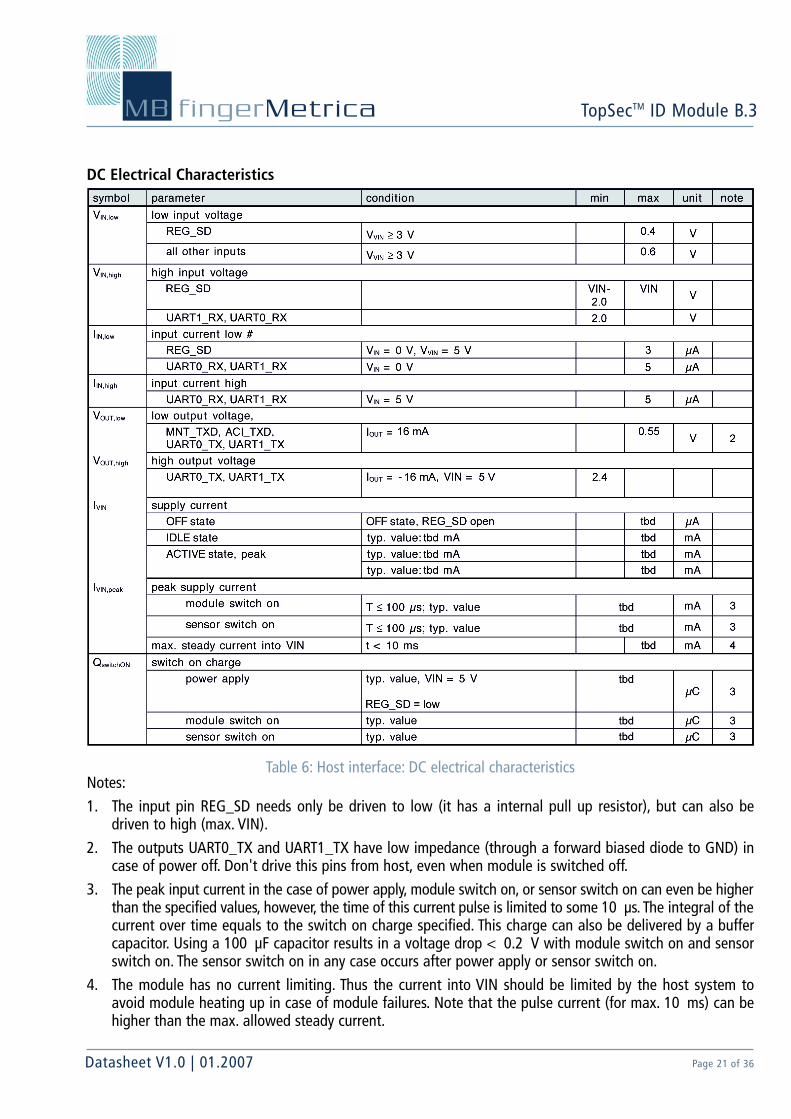
DC Electrical Characteristics
Table 6: Host interface: DC electrical characteristicsNotes:
1. The input pin REG_SD needs only be driven to low (it has a internal pull up resistor), but can also bedriven to high (max. VIN).
2. The outputs UART0_TX and UART1_TX have low impedance (through a forward biased diode to GND) incase of power off. Don't drive this pins from host, even when module is switched off.
3. The peak input current in the case of power apply, module switch on, or sensor switch on can even be higherthan the specified values, however, the time of this current pulse is limited to some 10 µs. The integral of thecurrent over time equals to the switch on charge specified. This charge can also be delivered by a buffercapacitor. Using a 100 µF capacitor results in a voltage drop < 0.2 V with module switch on and sensorswitch on. The sensor switch on in any case occurs after power apply or sensor switch on.
4. The module has no current limiting. Thus the current into VIN should be limited by the host system toavoid module heating up in case of module failures. Note that the pulse current (for max. 10 ms) can behigher than the max. allowed steady current.

TopSecTM ID Module B.3fingerMetricaMB
Datasheet V1.0 | 01.2007 Page 22 of 36
3.2. ATMEL Stripe Sensor InterfaceThe ATMEL sensor is connected to the TopSec ID Module B.3 through its 21 pin flex print connector (FPC) andis read out over its parallel data interface. Power supply is configured for ATMEL sensor usage.
The ATMEL sensor is connected to the TopSec ID Module B.3 through a 21 pin star flex cable.
The parallel data port of the ATMEL sensor (8 bit) is connected to the Parallel Port Interface (PPI) of the Black-fin processor.
The ATMEL sensor signals TPE, RST, PCLK, OE and ACKN are used according to the ATMEL sensor specification.
To avoid heating up of the sensor in the case of destruction (e.g. mechanical damage), and thus endanger theend user, the maximum sensor supply current has to be limited from the host power supply.
Attention: The sensor must not be plugged in or pulled out while the module is operating (switched on).Additional, it must be taken into consideration that this interface is basically not protected against ESD.
3.2.1. Sensor MalfunctionAs the sensor is accessible directly by the user it can be damaged (by very high ESD or mechanical influence).This can lead to short circuits on the sensor chip and to undefined high currents, which lead to an unwantedsystem load and a possibly high temperature of the sensor.
To avoid both effects, the supply current from the host for the sensor has to be limited to values beneath100mA.
ESD can also lead to reversible malfunction (non-destructive latch up).
3.3. External RAM/Flash memoryAs the external RAM/Flash memory the ATMEL 32 MB Flash + 8 MB PSRAM Stack Memory AT 52BC3221A(AT)is used. It’s I/0-Data bus is connected to the Blackfin processor data bus D(0.15). The chip is addressed throughthe Blackfin processor through its address bus.The processor selects specific memory areas through its available Chip Select signals.
3.4. ESDAs the sensor only has a thin coating upon the silicon, measures agianst ESD are an important issue.Following measures are provided by the module, or must be provided by the user of the module (OEM):
> The sensor has a metal frame, which is connected to the PG pins of its interface.
> The PG pins of the sensor interface are directly connected to the PG pins of the host interface. There is nogalvanic connection between PG and GND on the module.

TopSecTM ID Module B.3fingerMetricaMB
Datasheet V1.0 | 01.2007 Page 23 of 36
> The GND pins of all sensor interfaces are connected to the ground of the module (and therefore to the GNDpins of the host interface) through a small series resistor. In case of ESD the ground potential of thesensor raises and forces the discharge current flow through the PG pins.
> The user (OEM) must connect the PG pins of the host interface to GND at a ‘non-dangerous’ point. This isa point where no partial raise of the ground potential occurs – typically at the (big) bypassing capacitor ofthe power supply. The PG trace to this point must be as short as possible and must have low impedance.
> In the case of devices connected to earth typically with all devices supplied from the mains – the connectionto earth should be done from the same point, to avoid partial raise of the ground potential in the case of ESD.Any shields (metal, carbonized plastics, ...) must also be connected to ground at this point.
> If possible, the user should design the case of the final device in a manner that the end user first touchesa metal part of the case (connected to earth) before he touches the sensor (e.g. put the sensor in a kind of‘cave’ – this would also save the sensor from mechanical destruction).
Figure 4: ESD – Protection ground

It is recommended to connect the protection ground (PG) to the earth of the host adapter. In this case a connectionbetween GND and PG should be avoided. If there are no earth available (e.g. a battery system) the PG pin shouldbe connected to the GND pin at ‘non-dangerous’ point.
For all ESD and mechanical sensor design in also refer to ATMEL sensor specifications <4.1>.
3.5. Direct User InterfaceThere are no onboard LED’s on the TopSec ID Module B.x.
3.6. Power ManagementTo reduce power consumption when the module is not used, especially in battery powered applications, themodule can be in one of three operational states.
For current consumption of the states see 3.1.11.
3.6.1. OFF State – Shut DownThe module is in this state,> when the REG_SD line of the host interface is left open or driven high> in this mode the power consumption is about 3µA.
To leave this state, the REG_SD line must be driven low.
If this state isn´t used, the REG_SD line can permanently be connected to GND.
It is not necessary to first stabilize the voltage on VIN and then switch on the module.
3.6.2. IDLE State – HibernateAfter having performed the requested action, the module automatically enters the IDLE state.All no longer usedparts are turned off (sensor, DSP) but the oscillators keep running. Therefore the module continues operationimmediately after an event (interrupt, interface activity, ...).
Power Consumption in Hibernate: 50 µA
After a programmable time without any action (non-activity) the Blackfin processor enters the Hibernatemode (FW controlled) and can be waked up again through activity on the CAN or both UART-interfaces.
In case of SPI or I2C or UART 0 (MNT) host control interface usage the interrupt line (Pin20, DROSEC/CAN_RX) hasto be activated to wake up the Blackfin processor.
The Blackfin processor wakes up, when it detects activity on the CAN_RX line (change from 1 to zero). UART0and UART1 RX activity also wakes up the processor.
Hibernate reaction time: tbdSleep after non-activity: tbd during FW development
TopSecTM ID Module B.3fingerMetricaMB
Datasheet V1.0 | 01.2007 Page 24 of 36

TopSecTM ID Module B.3fingerMetricaMB
Datasheet V1.0 | 01.2007 Page 25 of 36
3.6.3. ACTIVE StateAfter power up or leaving the other states, the module is in active state. All necessary parts are active. Thecurrent consumption depends on the actual activity. (maximum 200 mA at 3.3 V, when sensor is active.)
3.7. ResetAfter supplying the external voltage to the board the supervising circuit generates a delayed reset (delay 250ms for internal voltage stabilization) for the Blackfin processor and the memory components.The processor will be reset and restarts. Simultaneously the external RAM/Flash device will also be reset.
A manual reset function at Pin 4 (host connector) is available (option).The processor controls the reset of the connected sensors through a GPIO signal.
For the ATMEL sensor the sensor reset signal is high active (signal is pulled down to GND).
In the Hibernate mode the connected sensor is reset.
3.8. Application Examples
3.8.1. Host Controlled Mode – Single Host System
Figure 5: Application example 1 for host controlled mode
Figure 5 shows a simple integration example for the ID Module B.x to an embedded host system. This appli-cation will be usable for enrollment process and an identification process as well. The software of the hostsystem should by separated into applications for administration (e.g. enrollment, archive update) and user(e.g. identification) for controlling the ID Module access. The handling of the access rights of these applicationsare also part of the host software, that means the access (e.g. positioning system of a seat, door lock) after asuccessful identification process must be done by the host.

TopSecTM ID Module B.3fingerMetricaMB
Datasheet V1.0 | 01.2007 Page 26 of 36
3.8.2. Host Controlled Mode – Double Host System
Figure 6: Application example 2 for host controlled mode
The ID Module B.x supports two serial host interfaces. The UART1 interface can be used for an embedded hostsystem like a micro controller and the UART0 can be used as maintenance interface for FW download from aPC for example.
Note: Only one host can have access to the ID Module B.x at the same time (first come first serve principle).
3.8.2.1. Interface RS232/RS485/RS422Both host interfaces of the ID Module B.x (UART0, UART1) are specified for TTL-Level. If the ID Module will beintegrated to a host with a RS232, RS485 or RS422 interface, a few external components are necessary.
Figure 7: Interface circuits
TopSecTM ID Module B.3fingerMetricaMB
Datasheet V1.0 | 01.2007 Page 27 of 36
3.8.3. Autonomous ModeThe autonomous mode operation for TopSec ID Module B.x is to be defined on a project specific basis. There areno on board LED’s available. There is also no open collector output available.
The autonomous mode of TopSec B.x could be implemented in a similar way as for TopSec A1 using availableGPIO Lines.
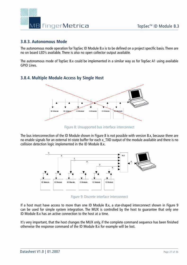
3.8.4. Multiple Module Access by Single Host
Figure 8: Unsupported bus interface interconnect
The bus interconnection of the ID Module shown in Figure 8 is not possible with version B.x, because there areno enable signals for an external tri-state buffer for each x_TXD output of the module available and there is nocollision detection logic implemented in the ID Module B.x.
Figure 9: Discrete interface interconnect
If a host must have access to more than one ID Module B.x, a star-shaped interconnect shown in Figure 9can be used for simple system integration. The MUX is controlled by the host to guarantee that only oneID Module B.x has an active connection to the host at a time.
It's very important, that the host changes the MUX only, if the complete command sequence has been finishedotherwise the response command of the ID Module B.x for example will be lost.
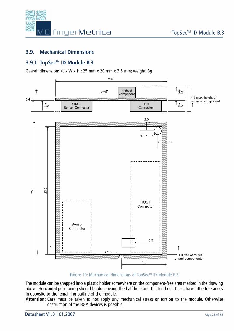
3.9. Mechanical Dimensions
3.9.1. TopSecTM ID Module B.3Overall dimensions (L x W x H): 25 mm x 20 mm x 3,5 mm; weight: 3g
Figure 10: Mechanical dimensions of TopSecTM ID Module B.3
The module can be snapped into a plastic holder somewhere on the component-free area marked in the drawingabove. Horizontal positioning should be done using the half hole and the full hole. These have little tolerancesin opposite to the remaining outline of the module.Attention: Care must be taken to not apply any mechanical stress or torsion to the module. Otherwise
destruction of the BGA devices is possible.
TopSecTM ID Module B.3fingerMetricaMB
Datasheet V1.0 | 01.2007 Page 28 of 36
ÝÝ
R 1.5
ÝR 1.5
2.0
2.0
2.2
23.0
ÝÝ
2.2
ÝÝÝÝ
Ý
Ý Ý
Ý
ÝÝ
Ý
ÝÝ
5.5
1.0 free of routesand components
HOSTConnector
SensorConnector
Ý Ý
8.5Ý Ý+
+
25.0
Ý
Ý
ATMELSensor Connector
HostConnector
highestcomponentPCB
20.0Ý Ý
Ý
Ý
4.8 max. height ofmounted component
2.2
0.4
Ý

TopSecTM ID Module B.3fingerMetricaMB
Datasheet V1.0 | 01.2007 Page 29 of 36
Ý
ÝÝ
HOST connector30 pin
Sensor connector21 pin
TopSec ID Module B.3ATMEL
stripe areaContact area
Ý
Ý
ÝÝContact area
3.9.2. Position of Flexible PCB InterconnectFor the host interface a FFC/FPC connector with 0,5 mm pitch, bottom contact and zero force is used. For the connec-tion from TopSec B.x to ATMEL sensor a 21 pin connector (0,3 mm pitch, bottom contact) is used.
Figure 11: Position of the flexprint connection
Figure 11 shows the right position for connecting the flexprint cables of the ATMEL sensor or the host interfacesto the related connectors of the ID Module PCB.The OEM integrators will source the HOST flexprint cable themselves. It is not included in our delivery (diffe-rent contact sides and length are possible).For the star flex cable to the sensor we can supply a standard cable (50 mm, contacts same side), if required(refer to Fig. 11).
3.9.3. ATMEL Stripe Sensor
Figure 12: B.3 with ATMEL Thermal Fingerprint Sensor (both backside)
Figure 13: Product Package

TopSecTM ID Module B.3fingerMetricaMB
Datasheet V1.0 | 01.2007 Page 30 of 36
3.9.4. ATMEL FingerChipTM Module AssemblyIn order to guarantee a reliable recognition of the fingerprint, the finger must be pulled over the sensor in aflat manner. We recommend guiding the finger position by means of a special physical surface design.The design should be done in a way, that a finger can be pulled easily over the entire sensor area at the timean image is read. Thus, the sensor location should not be positioned too deep compared to the remaining systemsurface. An example system design is outlined in the following picture.
Figure 14: System design for ATMEL FingerChipTM
3.9.5. Checklist for a ATMEL FingerChipTM Module AssemblySummarizing the information of the previous chapter, the following items should be taken into account for themechanical integration of a ATMEL module in a system:
> The finger positioning should be in a way, that the finger can be pulled over the entire sensor area.
> The sensor location should not lie too deep with respect to the remaining system surface.
> The housing should have immersions for globetop and for the capacitance. These should be at thecorresponding positions.
> The finger pulling over the sensor during the enrolment procedure and the identification procedure musthave the same direction. This is very important if the module assembly for the enrollment station and theidentification station is not the same. The sensor itself has no position preferences for reading the image.
> The finger positioning assembly should be designed for the populace.
Bild ATMEL USB device

TopSecTM ID Module B.3fingerMetricaMB
Datasheet V1.0 | 01.2007 Page 31 of 36
3.9.6. Alignment and Fixing of the ATMEL FingerChipTM in a System

TopSecTM ID Module B.3fingerMetricaMB
Datasheet V1.0 | 01.2007 Page 32 of 36
3.10. Environmental Qualification
3.10.1. Climate QualificationOperating temperature -40°C to + 70°C
Storage temperature -40°C to + 85°C
The qualification for operation conditions of the ID Module B.3 board was done in a typical test applicationaccording to the following standards:
Table 7: Climate qualification, operating conditions
Note:1. The quality of the sensor-imaging depends of humidity of the finger which toughs on the sensor-surface.
Therefore the functionality of the module where the sensor is readout (f. e. identification, enrolment, ...) isonly possible if there is no condensing water on the sensor-surface.
Qualification for storage and transportation of the packed ID Module B.3 board was done according to thefollowing standards:
Table 8: Climate qualification, storage and transportation
All details for ATMEL sensor climate qualification are described in <4.2>.

TopSecTM ID Module B.3fingerMetricaMB
Datasheet V1.0 | 01.2007 Page 33 of 36
3.10.2. Mechanical QualificationThe qualification of the unpacked ID Module B.3 board was done according to the following standards:
Table 9: Mechanical qualification
All details for ATMEL sensor mechanical qualification are described in <4.2>.
3.10.3. EMC-/ESD-QualificationThe measurement for EMC-Emission of the ID Module B.3 board was done in a typical test application accordingto the following standards:
Table 10: Radiated emission
The qualification for EMC-/ ESD-Immunity of the ID Module B.3 board was done in a typical test application1)
according to the following standards:
Table 11: Radiated immunity

TopSecTM ID Module B.3fingerMetricaMB
Datasheet V1.0 | 01.2007 Page 34 of 36
Table 12: Electrostatic discharge
*All details for ESD immunity of the ATMEL sensor are described in <4.2>.
3.10.4. Corrosive Gas AtmosphereThe qualification of the ID Module B.3 board was done according to the following standard:
Table 13: Corrosive gas atmosphere
3.10.5. Sensor Sunlight ResistanceFor details refer to <4.2>.
3.10.6. Sensor Chemical ResistanceFor details refer to <4.2>.
*

TopSecTM ID Module B.3fingerMetricaMB
Datasheet V1.0 | 01.2007 Page 35 of 36
3.10.7. Sensor Abrasive Resistance / Simulated Finger Touch TestFor details refer to <4.2>.
3.10.8. Sensor Scratch Resistance / Impact ResistanceFor details refer to <4.2>.
3.10.9. Product SafetyConformity according to EN 60950 (1997-11) and ICE 60950 (third edition, 1999-04) tested by TÜV-Austria.
Only SELV circuits must be used for both DC supply and interface circuits of the ID Module.
3.10.10. Environmental CompatibilityThe module contains no toxic substances. However, it must not be disposed to the household waste, but mustbe disposed as electronics scrap.
3.10.11. Standards, Approvals, MarkingsThe ID Module is no end user device by the intention of European standards (CE). It is a module to be built ininto end user equipment by an OEM. Nevertheless the module is prepared to meet the standards in an end userequipment, of course. The module and sensor is fully RoHS compliant.
3.10.12. Notes on EMC/ESDThe module is generally an ESD sensitive device and has to be handled with the appropriate precautions. Onlysome pins of the interfaces are dedicated for use as an interface to the environment and therefore protectedagainst ESD. These pins are marked explicitly in the interface description. ESD resistance of these pins accordsto EN50082-2.
Most interface pins are dedicated to be connected only to short wires (should not exceed 10 cm) as needed toconnect the module to a host system. Only the pins UART0_RX and UART1_TX of the host interface areintended to connect to a longer cable to a RS232 transceiver (should not exceed approx. 50 cm).
The overall length of the cable from the module to the PC (including the RS232 transceiver and the "RS232-side" of the cable) must not exceed 2 m. Otherwise special measures must be provided at the cable to reducethe electromagnetic radiation.
TopSecTM ID Module B.3fingerMetricaMB
Datasheet V1.0 | 01.2007 Page 36 of 36
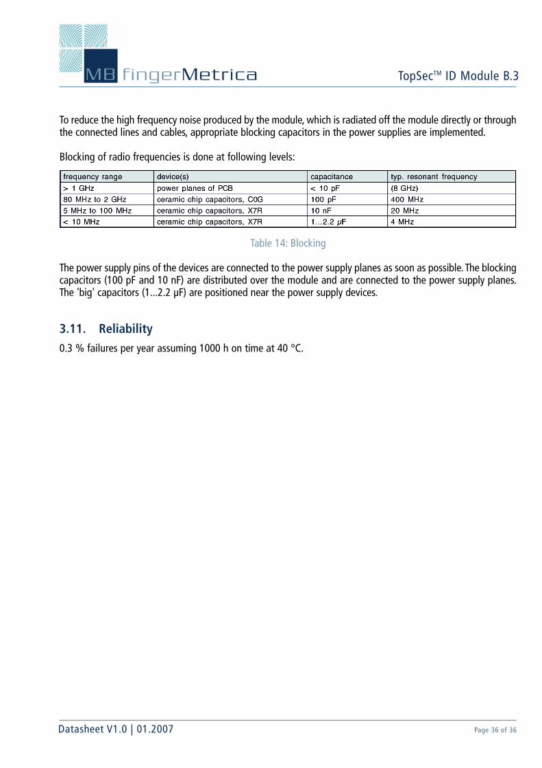
To reduce the high frequency noise produced by the module, which is radiated off the module directly or throughthe connected lines and cables, appropriate blocking capacitors in the power supplies are implemented.
Blocking of radio frequencies is done at following levels:
Table 14: Blocking
The power supply pins of the devices are connected to the power supply planes as soon as possible. The blockingcapacitors (100 pF and 10 nF) are distributed over the module and are connected to the power supply planes.The 'big' capacitors (1...2.2 µF) are positioned near the power supply devices.
3.11. Reliability0.3 % failures per year assuming 1000 h on time at 40 °C.

![Specification of Module XCP - AUTOSARSpecification of Module XCP AUTOSAR Release 4.2.2. 22 of 65 Document ID 412: AUTOSAR_SWS_XCP. - AUTOSAR confidential -. [SWS_Xcp_00707] ⌈The](https://img.pdfslide.us/doc/110x75/61327d96dfd10f4dd73a7bdc/specification-of-module-xcp-autosar-specification-of-module-xcp-autosar-release.jpg)