Embed Size (px)
Citation preview
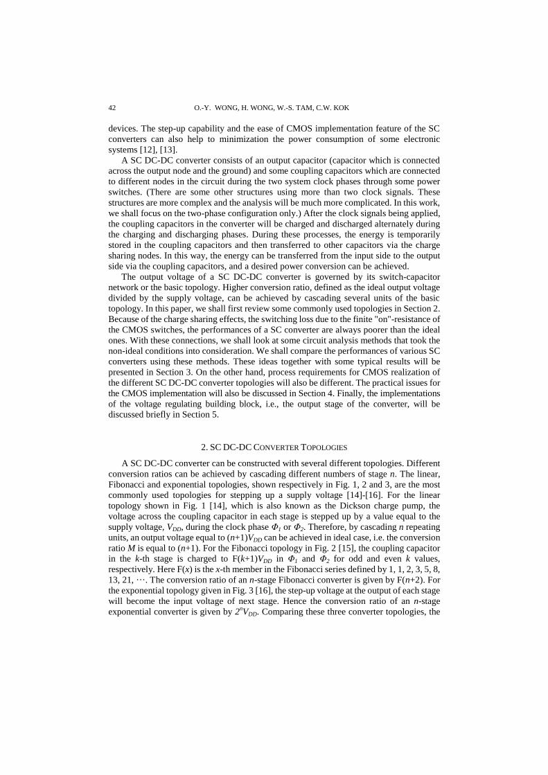
FACTA UNIVERSITATIS Series: Electronics and Energetics Vol. 27, No 1, March 2014, pp. 41 - 56 DOI: 10.2298/FUEE1401041W
TOPOLOGY, ANALYSIS, AND CMOS IMPLEMENTATION
OF SWITCHED-CAPACITOR DC-DC CONVERTERS
Oi-Ying Wong1, Hei Wong
1, Wing-Shan Tam
2, Chi-Wah Kok
2
1Department of Electronic Engineering, City University of Hong Kong, Tat Chee Avenue,
Kowloon, Hong Kong 2Canaan Semiconductor Ltd., Fotan, NT, Hong Kong
Abstract. This review highlights various design and realization aspects of three
commonly used charge pump topologies, namely, the linear, exponential, and the
Fibonacci type of charge pumps. We shall outline the new methods developed recently
for analyzing the steady and dynamic performances of these circuits. Some practical
issues for the CMOS implementation of these charge pump structures will be critically
discussed. Finally, some conventional voltage regulation methods for maintaining a
stable output under a large range of loading current and supply voltage fluctuations will
be proposed.
Key words: Switched-capacitor DC-DC converters, charge pump, steady-state analysis,
dynamic analysis, voltage regulation
1. INTRODUCTION
Switched-capacitor DC-DC converter (or SC DC-DC converter, in short) is a kind of
voltage converters which realizes a DC-to-DC voltage conversion using capacitors as the
only energy storage elements. Unlike the conventional inductor-based DC-DC converters,
no inductor is used in the SC DC-DC converters and that makes this kind of converter to
have less EMI emission, more compact in size, and is easier for system integration. When
compare with the low-dropout regulators (LDO) which can provide step-down conversion
only, the SC DC-DC converters have the advantage of being able to generate a voltage
higher than the supply. However, the conversion efficiency of a SC DC-DC converter is
usually poorer than those of inductor-based converters and the silicon area occupation of a
SC DC-DC converter is much larger than that of a LDO. Nevertheless, SC DC-DC
converters have been widely used for voltage generation in flash memory systems [1]-[3]
and LCD driver circuits where DC voltages higher than the supply voltages are required
[4], [5]. SC DC-DC converters are also used in energy harvesting system, self-powered
systems like biomedical implant devices, RFID, and wireless sensor networks [6]-[11]
where the available source voltages are too low to be used for operating any electronic
Received December 27, 2013 Corresponding author: Hei Wong
Department of Electronic Engineering,
City University of Hong Kong, Tat Chee Avenue, Kowloon, Hong Kong (e-mail: [email protected])
42 O.-Y. WONG, H. WONG, W.-S. TAM, C.W. KOK
devices. The step-up capability and the ease of CMOS implementation feature of the SC
converters can also help to minimization the power consumption of some electronic
systems [12], [13].
A SC DC-DC converter consists of an output capacitor (capacitor which is connected
across the output node and the ground) and some coupling capacitors which are connected
to different nodes in the circuit during the two system clock phases through some power
switches. (There are some other structures using more than two clock signals. These
structures are more complex and the analysis will be much more complicated. In this work,
we shall focus on the two-phase configuration only.) After the clock signals being applied,
the coupling capacitors in the converter will be charged and discharged alternately during
the charging and discharging phases. During these processes, the energy is temporarily
stored in the coupling capacitors and then transferred to other capacitors via the charge
sharing nodes. In this way, the energy can be transferred from the input side to the output
side via the coupling capacitors, and a desired power conversion can be achieved.
The output voltage of a SC DC-DC converter is governed by its switch-capacitor
network or the basic topology. Higher conversion ratio, defined as the ideal output voltage
divided by the supply voltage, can be achieved by cascading several units of the basic
topology. In this paper, we shall first review some commonly used topologies in Section 2.
Because of the charge sharing effects, the switching loss due to the finite "on"-resistance of
the CMOS switches, the performances of a SC converter are always poorer than the ideal
ones. With these connections, we shall look at some circuit analysis methods that took the
non-ideal conditions into consideration. We shall compare the performances of various SC
converters using these methods. These ideas together with some typical results will be
presented in Section 3. On the other hand, process requirements for CMOS realization of
the different SC DC-DC converter topologies will also be different. The practical issues for
the CMOS implementation will also be discussed in Section 4. Finally, the implementations
of the voltage regulating building block, i.e., the output stage of the converter, will be
discussed briefly in Section 5.
2. SC DC-DC CONVERTER TOPOLOGIES
A SC DC-DC converter can be constructed with several different topologies. Different
conversion ratios can be achieved by cascading different numbers of stage n. The linear,
Fibonacci and exponential topologies, shown respectively in Fig. 1, 2 and 3, are the most
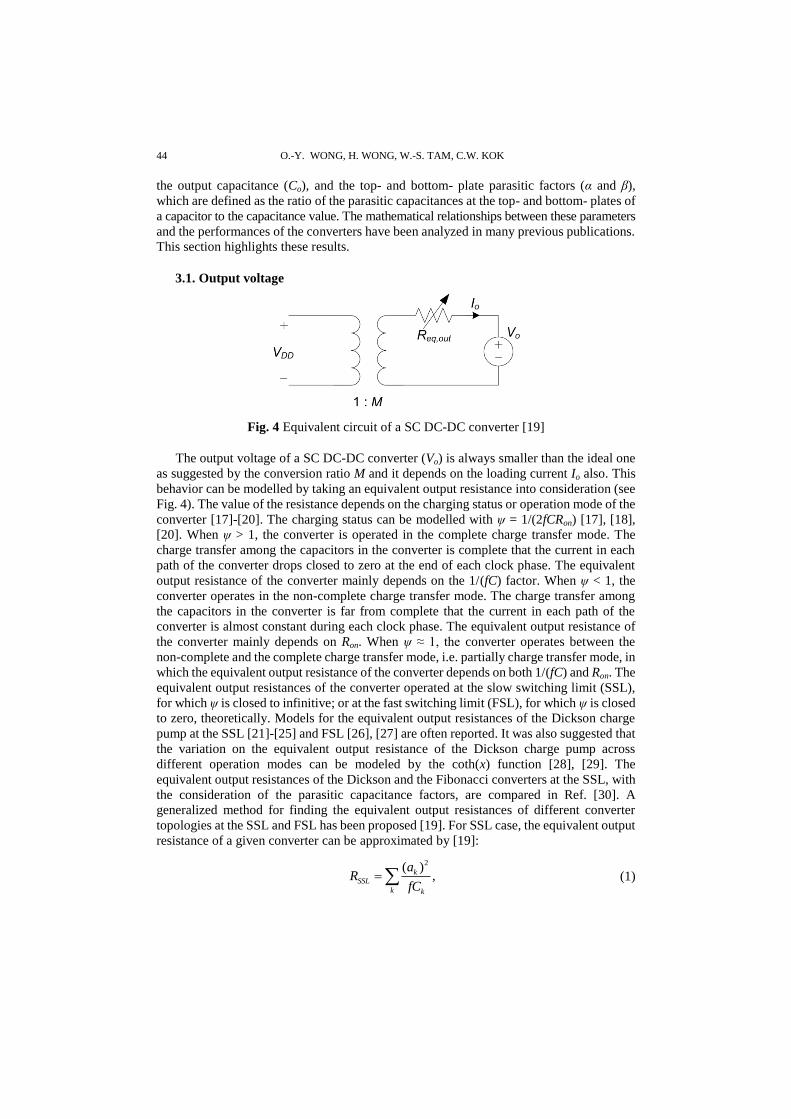
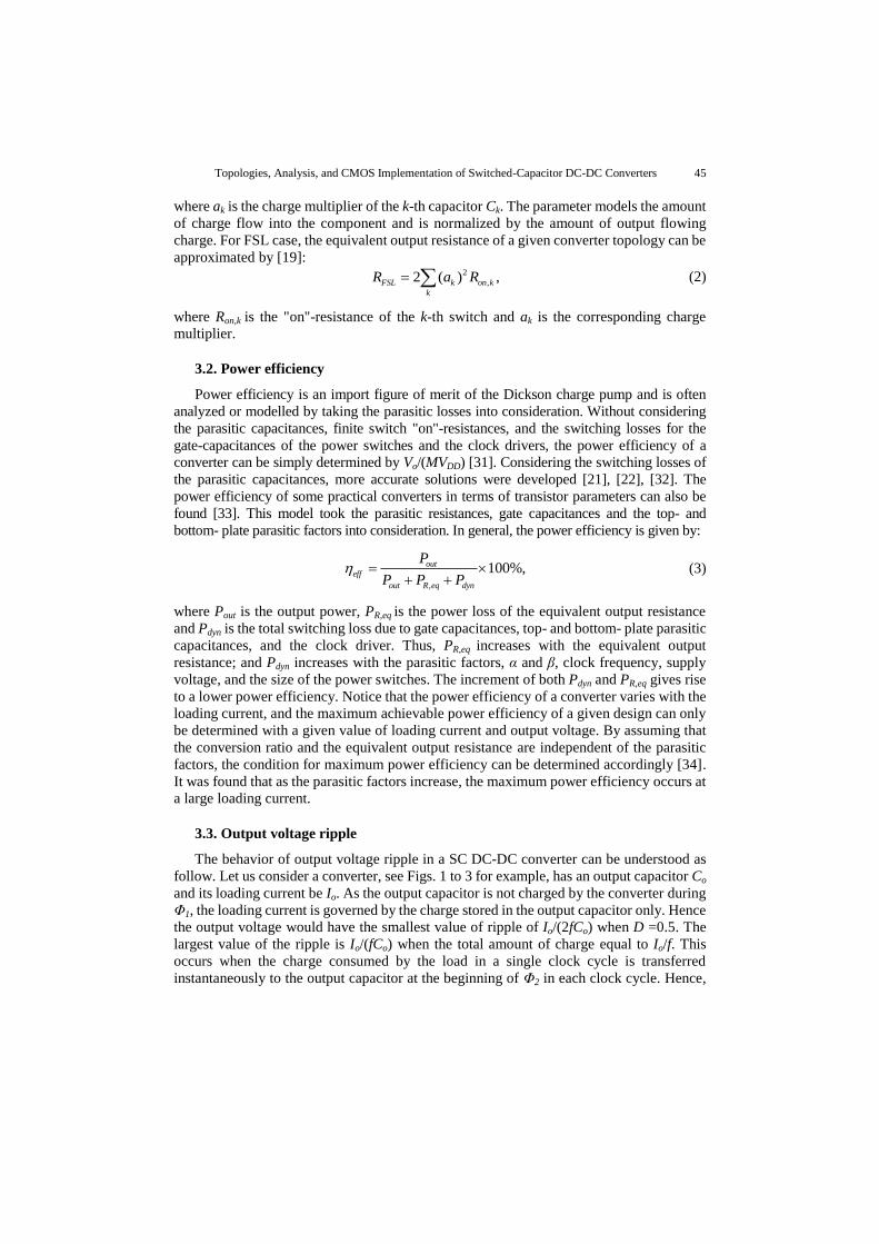
commonly used topologies for stepping up a supply voltage [14]-[16]. For the linear
topology shown in Fig. 1 [14], which is also known as the Dickson charge pump, the
voltage across the coupling capacitor in each stage is stepped up by a value equal to the
supply voltage, VDD, during the clock phase Φ1 or Φ2. Therefore, by cascading n repeating
units, an output voltage equal to (n+1)VDD can be achieved in ideal case, i.e. the conversion
ratio M is equal to (n+1). For the Fibonacci topology in Fig. 2 [15], the coupling capacitor
in the k-th stage is charged to F(k+1)VDD in Φ1 and Φ2 for odd and even k values,
respectively. Here F(x) is the x-th member in the Fibonacci series defined by 1, 1, 2, 3, 5, 8,
13, 21, ···. The conversion ratio of an n-stage Fibonacci converter is given by F(n+2). For
the exponential topology given in Fig. 3 [16], the step-up voltage at the output of each stage
will become the input voltage of next stage. Hence the conversion ratio of an n-stage
exponential converter is given by 2nVDD. Comparing these three converter topologies, the
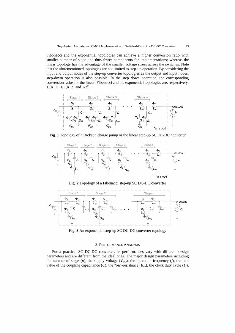
Topologies, Analysis, and CMOS Implementation of Switched-Capacitor DC-DC Converters 43
Fibonacci and the exponential topologies can achieve a higher conversion ratio with
smaller number of stage and thus fewer components for implementations; whereas the
linear topology has the advantage of the smaller voltage stress across the switches. Note
that the aforementioned topologies are not limited to step-up operation. By considering the
input and output nodes of the step-up converter topologies as the output and input nodes,
step-down operation is also possible. In the step down operation, the corresponding
conversion ratios for the linear, Fibonacci and the exponential topologies are, respectively,
1/(n+1), 1/F(n+2) and 1/2n.
Fig. 1 Topology of a Dickson charge pump or the linear step-up SC DC-DC converter
Fig. 2 Topology of a Fibonacci step-up SC DC-DC converter
Fig. 3 An exponential step-up SC DC-DC converter topology
3. PERFORMANCE ANALYSIS
For a practical SC DC-DC converter, its performances vary with different design
parameters and are different from the ideal ones. The major design parameters including
the number of stage (n), the supply voltage (VDD), the operation frequency (f), the unit
value of the coupling capacitance (C), the "on"-resistance (Ron), the clock duty cycle (D),
44 O.-Y. WONG, H. WONG, W.-S. TAM, C.W. KOK
the output capacitance (Co), and the top- and bottom- plate parasitic factors (α and β),
which are defined as the ratio of the parasitic capacitances at the top- and bottom- plates of
a capacitor to the capacitance value. The mathematical relationships between these parameters
and the performances of the converters have been analyzed in many previous publications.
This section highlights these results.
3.1. Output voltage
Fig. 4 Equivalent circuit of a SC DC-DC converter [19]
The output voltage of a SC DC-DC converter (Vo) is always smaller than the ideal one
as suggested by the conversion ratio M and it depends on the loading current Io also. This
behavior can be modelled by taking an equivalent output resistance into consideration (see
Fig. 4). The value of the resistance depends on the charging status or operation mode of the
converter [17]-[20]. The charging status can be modelled with ψ = 1/(2fCRon) [17], [18],
[20]. When ψ > 1, the converter is operated in the complete charge transfer mode. The
charge transfer among the capacitors in the converter is complete that the current in each
path of the converter drops closed to zero at the end of each clock phase. The equivalent
output resistance of the converter mainly depends on the 1/(fC) factor. When ψ < 1, the
converter operates in the non-complete charge transfer mode. The charge transfer among
the capacitors in the converter is far from complete that the current in each path of the
converter is almost constant during each clock phase. The equivalent output resistance of
the converter mainly depends on Ron. When ψ ≈ 1, the converter operates between the
non-complete and the complete charge transfer mode, i.e. partially charge transfer mode, in
which the equivalent output resistance of the converter depends on both 1/(fC) and Ron. The
equivalent output resistances of the converter operated at the slow switching limit (SSL),
for which ψ is closed to infinitive; or at the fast switching limit (FSL), for which ψ is closed
to zero, theoretically. Models for the equivalent output resistances of the Dickson charge
pump at the SSL [21]-[25] and FSL [26], [27] are often reported. It was also suggested that
the variation on the equivalent output resistance of the Dickson charge pump across
different operation modes can be modeled by the coth(x) function [28], [29]. The
equivalent output resistances of the Dickson and the Fibonacci converters at the SSL, with
the consideration of the parasitic capacitance factors, are compared in Ref. [30]. A
generalized method for finding the equivalent output resistances of different converter
topologies at the SSL and FSL has been proposed [19]. For SSL case, the equivalent output
resistance of a given converter can be approximated by [19]:
2( ),k
SSL
k k
aR
fC (1)
Topologies, Analysis, and CMOS Implementation of Switched-Capacitor DC-DC Converters 45
where ak is the charge multiplier of the k-th capacitor Ck. The parameter models the amount
of charge flow into the component and is normalized by the amount of output flowing
charge. For FSL case, the equivalent output resistance of a given converter topology can be
approximated by [19]:
2
,2 ( ) ,FSL k on k
k
R a R (2)
where Ron,k is the "on"-resistance of the k-th switch and ak is the corresponding charge
multiplier.
3.2. Power efficiency
Power efficiency is an import figure of merit of the Dickson charge pump and is often
analyzed or modelled by taking the parasitic losses into consideration. Without considering
the parasitic capacitances, finite switch "on"-resistances, and the switching losses for the
gate-capacitances of the power switches and the clock drivers, the power efficiency of a
converter can be simply determined by Vo/(MVDD) [31]. Considering the switching losses of
the parasitic capacitances, more accurate solutions were developed [21], [22], [32]. The
power efficiency of some practical converters in terms of transistor parameters can also be
found [33]. This model took the parasitic resistances, gate capacitances and the top- and
bottom- plate parasitic factors into consideration. In general, the power efficiency is given by:
,
100%,outeff
out R eq dyn
P
P P P
(3)
where Pout is the output power, PR,eq is the power loss of the equivalent output resistance
and Pdyn is the total switching loss due to gate capacitances, top- and bottom- plate parasitic
capacitances, and the clock driver. Thus, PR,eq increases with the equivalent output
resistance; and Pdyn increases with the parasitic factors, α and β, clock frequency, supply
voltage, and the size of the power switches. The increment of both Pdyn and PR,eq gives rise
to a lower power efficiency. Notice that the power efficiency of a converter varies with the
loading current, and the maximum achievable power efficiency of a given design can only
be determined with a given value of loading current and output voltage. By assuming that
the conversion ratio and the equivalent output resistance are independent of the parasitic
factors, the condition for maximum power efficiency can be determined accordingly [34].
It was found that as the parasitic factors increase, the maximum power efficiency occurs at
a large loading current.
3.3. Output voltage ripple
The behavior of output voltage ripple in a SC DC-DC converter can be understood as
follow. Let us consider a converter, see Figs. 1 to 3 for example, has an output capacitor Co
and its loading current be Io. As the output capacitor is not charged by the converter during
Φ1, the loading current is governed by the charge stored in the output capacitor only. Hence
the output voltage would have the smallest value of ripple of Io/(2fCo) when D =0.5. The
largest value of the ripple is Io/(fCo) when the total amount of charge equal to Io/f. This
occurs when the charge consumed by the load in a single clock cycle is transferred
instantaneously to the output capacitor at the beginning of Φ2 in each clock cycle. Hence,
46 O.-Y. WONG, H. WONG, W.-S. TAM, C.W. KOK
when a converter is operated in the complete charge transfer mode, its output voltage ripple
is more likely to be larger than the minimum value. On the other hand, the output voltage
ripple is closed to the minimum value when the converter is operated in the non-complete
charge transfer mode. A detailed discussion on the output voltage ripple under different
operation modes can be found in Ref. [20].
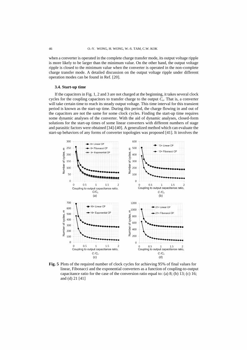
3.4. Start-up time
If the capacitors in Fig. 1, 2 and 3 are not charged at the beginning, it takes several clock
cycles for the coupling capacitors to transfer charge to the output Co. That is, a converter
will take certain time to reach its steady output voltage. This time interval for this transient
period is known as the start-up time. During this period, the charge flowing in and out of
the capacitors are not the same for some clock cycles. Finding the start-up time requires
some dynamic analyses of the converter. With the aid of dynamic analyses, closed-form
solutions for the start-up times of some linear converters with different numbers of stage
and parasitic factors were obtained [34]-[40]. A generalized method which can evaluate the
start-up behaviors of any forms of converter topologies was proposed [41]. It involves the
Fig. 5 Plots of the required number of clock cycles for achieving 95% of final values for
linear, Fibonacci and the exponential converters as a function of coupling-to-output
capacitance ratio for the case of the conversion ratio equal to: (a) 8; (b) 13; (c) 16;
and (d) 21 [41]
Topologies, Analysis, and CMOS Implementation of Switched-Capacitor DC-DC Converters 47
formulation of a given converter topology into some matrices, from which the output
voltage of a converter can be evaluated with time using the matrix equations. In the
analyses, we assume: (a) the converter is operated at SSL mode with capacitive loads only;
(b) all the capacitors in the converter are initially uncharged; (c) the parasitic capacitance
effects can be neglected. Based on these assumptions, the number of cycle, m, for
achieving 95% of final output value can be determined. Figure 5 plots the number of cycle
as a function of coupling-to-output capacitance ratio (defined by Co/C) for the case of n=8,
13, 16 and 21[41]. It can be found that for a converter to have a short start-up time, the
output capacitance should not be larger than 2 times of the coupling capacitance.
3.5. Performance comparison of different topologies
This section concludes with the performance comparison as given in Table 1. Table 1
lists the performances of the 8× linear, Fibonacci and exponential converter with same
conversion ratio. Note that the equivalent output resistance of the linear converter at the
FSL mode is smaller than those of the Fibonacci and the exponential ones. In addition, the
voltage stress across the transistors in the linear converter is smaller regardless the large
number of cascading stages. However, the linear converter requires larger number of
components to implement and has a longer start-up time. Further detailed comparison on
the performances of these kinds of converters can be found in Refs. [42], [43].
Table 1 Comparison of the linear, Fibonacci and exponential topologies with M = 8
Topology n No. of
switch
No. of
capacitor
Max. blocking
voltage (V)
Req,out Start-up time (no.
of clock cycle, m,
for C/Co=1) SSL
(1/(Cf))
FSL
(Ron)
Linear 7 22 7 2VDD 7 44 75
Fibonacci 4 13 4 5VDD 7 52 36
Exponential 3 12 5 4VDD 10 56 30
4. CMOS IMPLEMENTATION OF SC DC-DC CONVERTERS
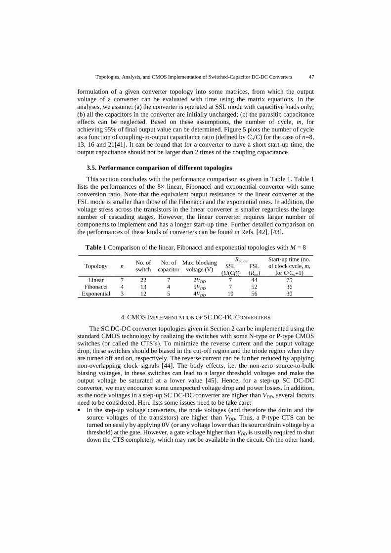
The SC DC-DC converter topologies given in Section 2 can be implemented using the standard CMOS technology by realizing the switches with some N-type or P-type CMOS switches (or called the CTS’s). To minimize the reverse current and the output voltage drop, these switches should be biased in the cut-off region and the triode region when they are turned off and on, respectively. The reverse current can be further reduced by applying non-overlapping clock signals [44]. The body effects, i.e. the non-zero source-to-bulk biasing voltages, in these switches can lead to a larger threshold voltages and make the output voltage be saturated at a lower value [45]. Hence, for a step-up SC DC-DC converter, we may encounter some unexpected voltage drop and power losses. In addition, as the node voltages in a step-up SC DC-DC converter are higher than VDD, several factors need to be considered. Here lists some issues need to be take care: In the step-up voltage converters, the node voltages (and therefore the drain and the
source voltages of the transistors) are higher than VDD. Thus, a P-type CTS can be turned on easily by applying 0V (or any voltage lower than its source/drain voltage by a threshold) at the gate. However, a gate voltage higher than VDD is usually required to shut down the CTS completely, which may not be available in the circuit. On the other hand,
48 O.-Y. WONG, H. WONG, W.-S. TAM, C.W. KOK
an N-type CTS can be readily shut down by applying 0V (or any voltage lower than its source/drain voltage plus a threshold) at the gate. However, to turn on the CTS completely, the gate voltage should be higher than VDD. The bodies (or the N-wells if the converter is implemented in an ordinary N-well process) of the P-type CTS's are usually required to be biased at a voltage higher than VDD such that the P-N junctions in the transistors can be always in reversely biased. Otherwise, substrate leakage current exists and the converter would have poor efficiency. On the other hand, if the bodies of the N-type CTS's are biased at 0V (which is the usual case for the circuits implemented in an ordinary N-well process), they will suffer from the body effect and that the threshold voltages of the CTS's will become larger. As the node voltages in the linear topology increase linearly from the input side to the output, while those in the other ones can rise exponentially. Thus, it is easier to design an efficient converter using the linear topology.
Fig. 6 Illustration of the three gate-biasing techniques: (a) the dynamic biasing;
(b) gate-boosting; and (c) the cross-coupled techniques [46]-[49]
Fig. 7 Illustration of the three body-biasing approaches: the (a) floating-well; (b) adaptive
body-biasing; and the (c) body-source junction diode approaches [50]-[52]
Topologies, Analysis, and CMOS Implementation of Switched-Capacitor DC-DC Converters 49
In the step-down voltage converters, the node voltages (and therefore the drain and the
source voltages of the transistors) are between 0V and VDD. Thus, the body and the
gate terminals of both N- and P-type CTS's can be biased properly without any
difficulties. However, the use of N-type CTS can usually save more silicon area due to
its higher transconductance. To pass a voltage in the range of 0V to VDD, transmission
gates can be used.
To achieve higher power efficiency, several different gate- and body- basing
techniques have been proposed to control the CTS’s in the Dickson charge pump. Figure 6
shows the dynamic biasing [46], gate boosting [47], [48] and the cross-coupled techniques
[49] for gate biasing. Figure 7 shows some techniques including the floating-well [50],
adaptive body-biasing [51], and the body-source junction diode approach [52], to alleviate
the body effects of the CTS. The advantages and disadvantages of these techniques have
been discussed in detail in Ref. [53]. In short, small output voltage drops can be found in
the converters using the gate boosting and the cross-coupled techniques, but the
gate-boosting technique would consume larger dynamic power and the cross-coupled
technique requires a costive triple-well process. Advanced converter circuits are usually
constructed by making use of more than one of these techniques [54], [55].
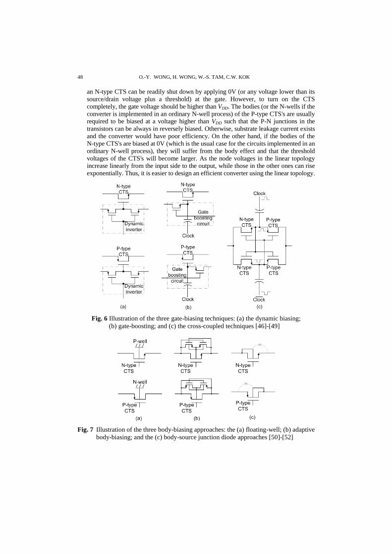
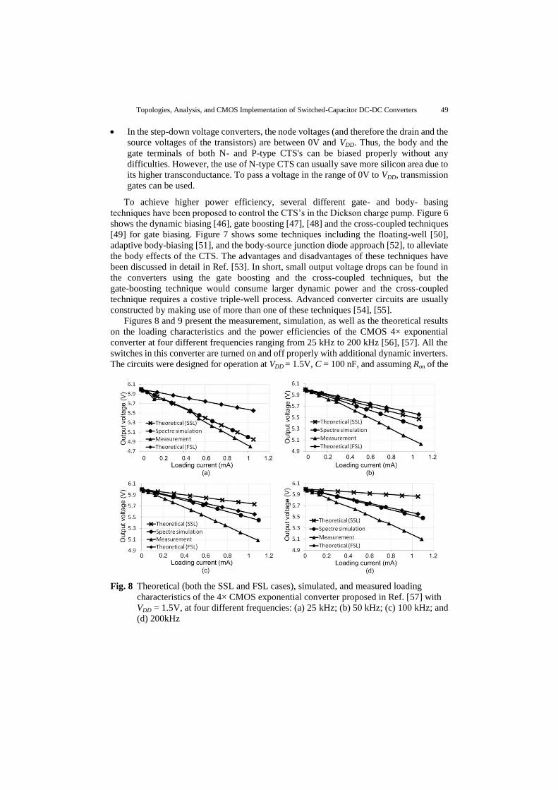
Figures 8 and 9 present the measurement, simulation, as well as the theoretical results
on the loading characteristics and the power efficiencies of the CMOS 4× exponential
converter at four different frequencies ranging from 25 kHz to 200 kHz [56], [57]. All the
switches in this converter are turned on and off properly with additional dynamic inverters.
The circuits were designed for operation at VDD = 1.5V, C = 100 nF, and assuming Ron of the
Fig. 8 Theoretical (both the SSL and FSL cases), simulated, and measured loading
characteristics of the 4× CMOS exponential converter proposed in Ref. [57] with
VDD = 1.5V, at four different frequencies: (a) 25 kHz; (b) 50 kHz; (c) 100 kHz; and
(d) 200kHz
50 O.-Y. WONG, H. WONG, W.-S. TAM, C.W. KOK
switches be 50 Ω. For f = 25 kHz, 50 kHz, 100 kHz and 200 kHz, the corresponding ψ
values are equal to 4, 2, 1 and 0.5, respectively. Thus, it is expected that the designed
converter is more likely to be operated at the SSL mode with Req,out given by eq. (1) for f =
25 kHz and 50 kHz. For f = 100 kHz and 200 kHz, they are at FSL mode and Req,out is given
by eq. (2). The simulation results shown in Fig. 8 agree well with this conjecture. In Fig. 8,
loading characteristics are more or less the same. It further prove that the designed circuit
should work at the FSL when f = 100 kHz and 200 kHz. It is because the equivalent output
resistance of a converter at FSL should be independent of the operation frequency
according to eq. (2). The difference between the theoretical and the measurement results in
Fig. 8(a)-(d) should be due to the equivalent series resistance (ESR) of the externally
connected capacitors, interconnections, and the parasitic capacitances at each node of the
real circuit. This difference is less than 10% [57]. In Fig. 9, it can be further observed that
when the frequency is increased from 25 kHz to 200 kHz, the measured power efficiency
drops from 80% to 40% when the loading current is small. This agrees well with what
suggested by eq. (3). In eq. (3), the dynamic power loss, Pdyn, dominates when the output
power is small, and Pdyn increases with the operation frequency [57].
Fig. 9 Theoretical and measured power efficiencies versus loading current of the 4×
CMOS exponential converter proposed in Ref. [57] with VDD = 1.5 V, at four
different frequencies: (a) 25 kHz; (b) 50 kHz; (c) 100 kHz; and (d) 200 kHz
Topologies, Analysis, and CMOS Implementation of Switched-Capacitor DC-DC Converters 51
5. REGULATIONS IN SC DC-DC CONVERTERS
As shown in Fig. 8, the output voltages of the SC DC-DC converters drop as the loading
currents increase. To maintain a constant output voltage under different loads, a better
regulation method that using a closed-loop structure is required for the SC DC-DC
converters. On the other hand, the supply voltage, like the battery used in some portable
devices, may also drop significantly during the operation and that causes the output voltage
of the DC-DC converters to drop continuously as the output voltage of a SC DC-DC
converter is directly proportional to the supply voltage. Hence, we need to maintain the
output voltage over a wide supply voltage range also. These are the main tasks for the
output stage of the converters. In this section, a review on some previously proposed
regulation techniques will be given.
5.1. Regulation for loading current fluctuation
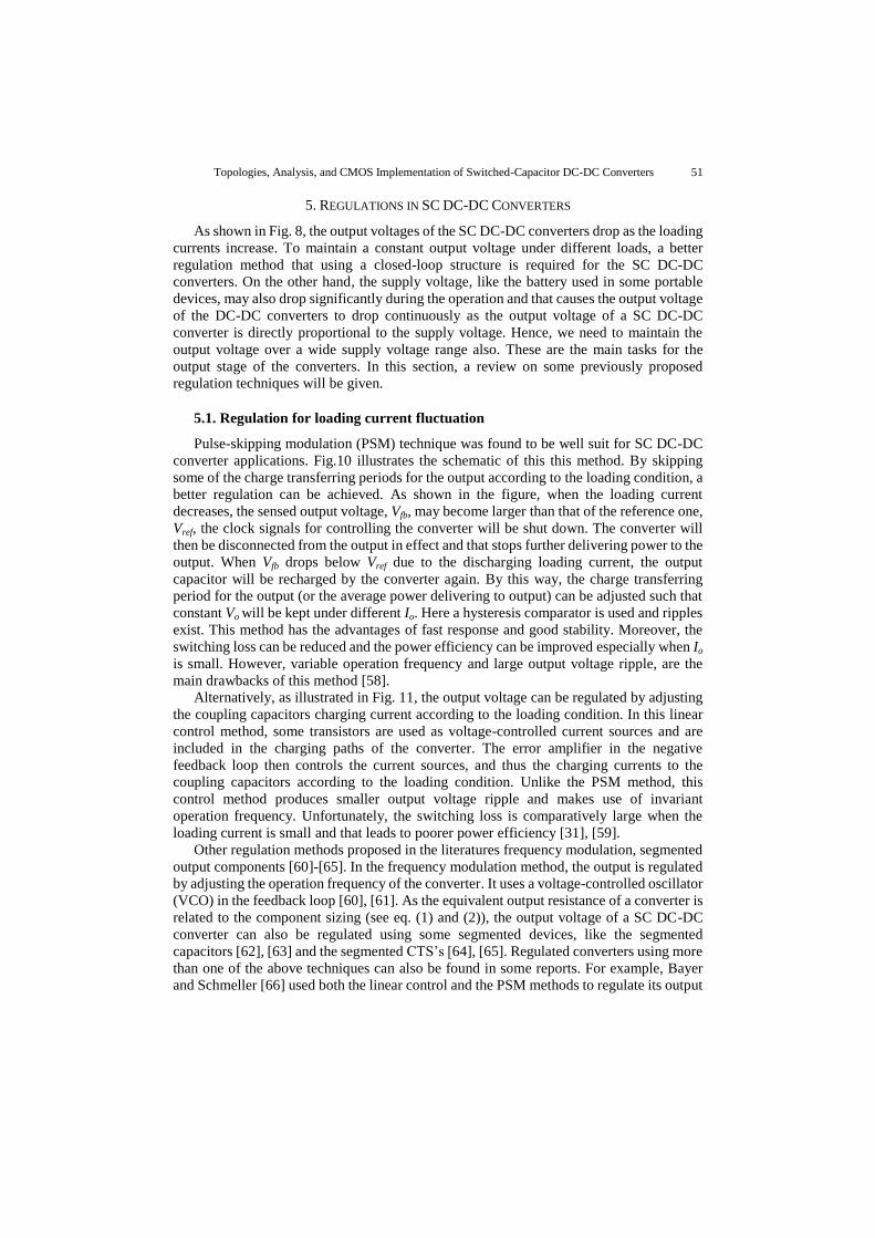
Pulse-skipping modulation (PSM) technique was found to be well suit for SC DC-DC
converter applications. Fig.10 illustrates the schematic of this this method. By skipping
some of the charge transferring periods for the output according to the loading condition, a
better regulation can be achieved. As shown in the figure, when the loading current
decreases, the sensed output voltage, Vfb, may become larger than that of the reference one,
Vref, the clock signals for controlling the converter will be shut down. The converter will
then be disconnected from the output in effect and that stops further delivering power to the
output. When Vfb drops below Vref due to the discharging loading current, the output
capacitor will be recharged by the converter again. By this way, the charge transferring
period for the output (or the average power delivering to output) can be adjusted such that
constant Vo will be kept under different Io. Here a hysteresis comparator is used and ripples
exist. This method has the advantages of fast response and good stability. Moreover, the
switching loss can be reduced and the power efficiency can be improved especially when Io
is small. However, variable operation frequency and large output voltage ripple, are the
main drawbacks of this method [58].
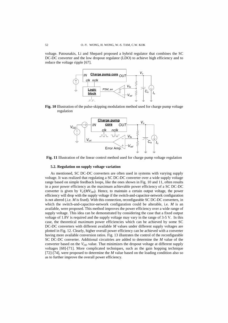
Alternatively, as illustrated in Fig. 11, the output voltage can be regulated by adjusting
the coupling capacitors charging current according to the loading condition. In this linear
control method, some transistors are used as voltage-controlled current sources and are
included in the charging paths of the converter. The error amplifier in the negative
feedback loop then controls the current sources, and thus the charging currents to the
coupling capacitors according to the loading condition. Unlike the PSM method, this
control method produces smaller output voltage ripple and makes use of invariant
operation frequency. Unfortunately, the switching loss is comparatively large when the
loading current is small and that leads to poorer power efficiency [31], [59].
Other regulation methods proposed in the literatures frequency modulation, segmented
output components [60]-[65]. In the frequency modulation method, the output is regulated
by adjusting the operation frequency of the converter. It uses a voltage-controlled oscillator
(VCO) in the feedback loop [60], [61]. As the equivalent output resistance of a converter is
related to the component sizing (see eq. (1) and (2)), the output voltage of a SC DC-DC
converter can also be regulated using some segmented devices, like the segmented
capacitors [62], [63] and the segmented CTS’s [64], [65]. Regulated converters using more
than one of the above techniques can also be found in some reports. For example, Bayer
and Schmeller [66] used both the linear control and the PSM methods to regulate its output
52 O.-Y. WONG, H. WONG, W.-S. TAM, C.W. KOK
voltage. Patounakis, Li and Shepard proposed a hybrid regulator that combines the SC
DC-DC converter and the low dropout regulator (LDO) to achieve high efficiency and to
reduce the voltage ripple [67].
Fig. 10 Illustration of the pulse-skipping modulation method used for charge pump voltage
regulation
Fig. 11 Illustration of the linear control method used for charge pump voltage regulation
5.2. Regulation on supply voltage variation
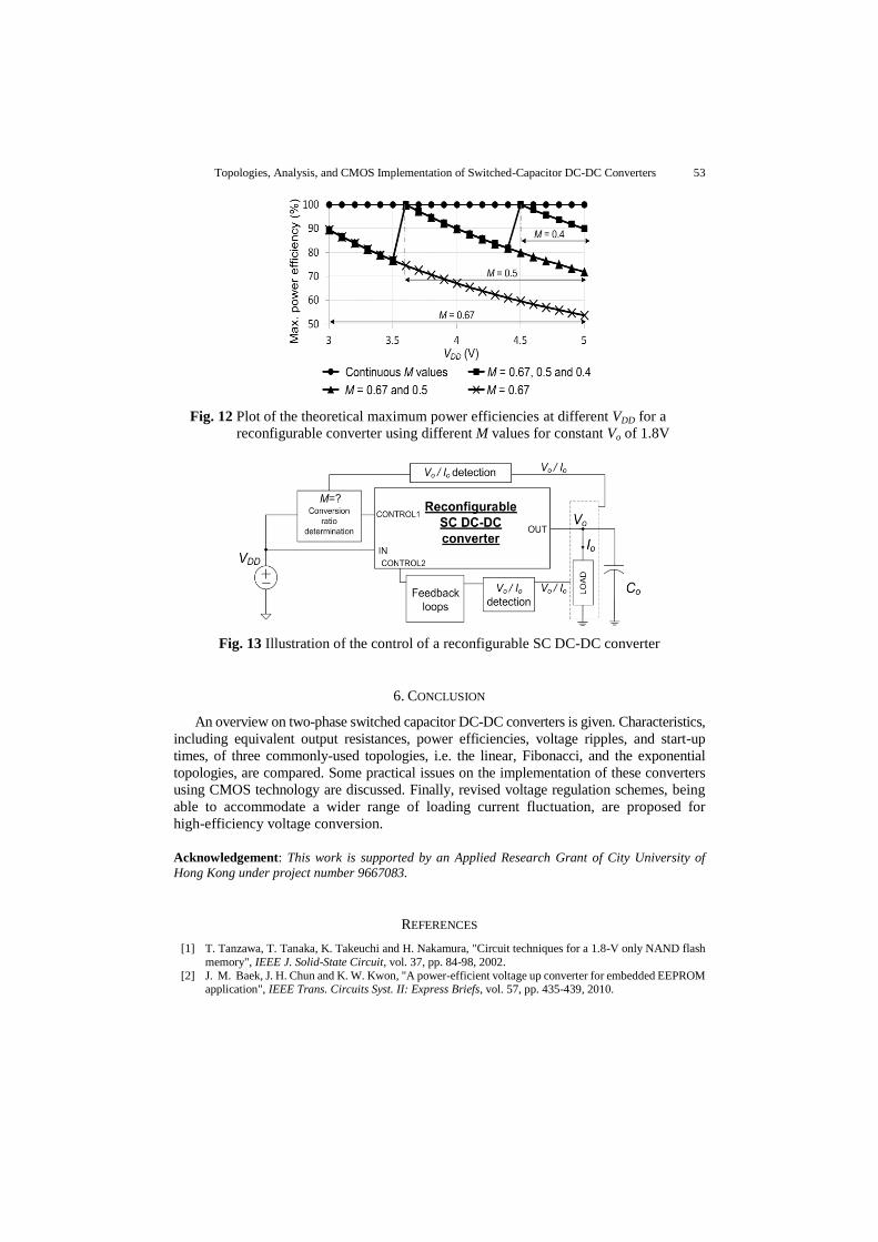
As mentioned, SC DC-DC converters are often used in systems with varying supply
voltage. It was realized that regulating a SC DC-DC converter over a wide supply voltage
range based on simple feedback loops, like the ones shown in Fig. 10 and 11, often results
in a poor power efficiency as the maximum achievable power efficiency of a SC DC-DC
converter is given by Vo/(MVDD). Hence, to maintain a certain output voltage, the power
efficiency will drop with the supply voltage if the switch-and-capacitor-network configuration
is not altered (.i.e. M is fixed). With this connection, reconfigurable SC DC-DC converters, in
which the switch-and-capacitor-network configuration could be alterable, i.e. M is an
available, were proposed. This method improves the power efficiency over a wide range of
supply voltage. This idea can be demonstrated by considering the case that a fixed output
voltage of 1.8V is required and the supply voltage may vary in the range of 3-5 V. In this
case, the theoretical maximum power efficiencies which can be achieved by some SC
DC-DC converters with different available M values under different supply voltages are
plotted in Fig. 12. Clearly, higher overall power efficiency can be achieved with a converter
having more available conversion ratios. Fig. 13 illustrates the control of the reconfigurable
SC DC-DC converter. Additional circuitries are added to determine the M value of the
converter based on the VDD value. That minimizes the dropout voltage at different supply
voltages [68]-[71]. More complicated techniques, such as the gain hopping technique
[72]-[74], were proposed to determine the M value based on the loading condition also so
as to further improve the overall power efficiency.
Topologies, Analysis, and CMOS Implementation of Switched-Capacitor DC-DC Converters 53
Fig. 12 Plot of the theoretical maximum power efficiencies at different VDD for a
reconfigurable converter using different M values for constant Vo of 1.8V
Fig. 13 Illustration of the control of a reconfigurable SC DC-DC converter
6. CONCLUSION
An overview on two-phase switched capacitor DC-DC converters is given. Characteristics,
including equivalent output resistances, power efficiencies, voltage ripples, and start-up
times, of three commonly-used topologies, i.e. the linear, Fibonacci, and the exponential
topologies, are compared. Some practical issues on the implementation of these converters
using CMOS technology are discussed. Finally, revised voltage regulation schemes, being
able to accommodate a wider range of loading current fluctuation, are proposed for
high-efficiency voltage conversion.
Acknowledgement: This work is supported by an Applied Research Grant of City University of
Hong Kong under project number 9667083.
REFERENCES
[1] T. Tanzawa, T. Tanaka, K. Takeuchi and H. Nakamura, "Circuit techniques for a 1.8-V only NAND flash
memory", IEEE J. Solid-State Circuit, vol. 37, pp. 84-98, 2002.
[2] J. M. Baek, J. H. Chun and K. W. Kwon, "A power-efficient voltage up converter for embedded EEPROM application", IEEE Trans. Circuits Syst. II: Express Briefs, vol. 57, pp. 435-439, 2010.
54 O.-Y. WONG, H. WONG, W.-S. TAM, C.W. KOK
[3] N. Derhacobian, S. C. Hollmer, N. Gilbert and M. N. Kozicki, "Power and energy perspectives of
nonvolatile memory technologies", Proc. IEEE, vol. 98, pp. 283-29, 2010. [4] C.-H. Wu and C.-L. Chen, "Multiphase charge pump generating positive and negative voltages for
TFT-LCD gate driving", in IEEE Int. Symp. Electronic Design, Test and Appl., pp. 179-183, 2008.
[5] F. Su and W.-H. Ki, "Component-efficient multiphase switched-capacitor DC-DC converter with configurable conversion ratios for LCD driver applications", IEEE Trans. Circuits Syst. II: Express Briefs,
vol. 5, pp. 753-757, 2008.
[6] W. Zhao, K. Choi, S. Baumana, Z. Dilli, T. Salter and M. Peckerar, "A radio-frequency energy harvesting scheme for use in low power Ad Hoc distributed network", IEEE Trans. Circuits Syst. II: Express Briefs,
vol. 59, pp. 573-577, 2012.
[7] T. Salter, K. Choi, M. Peckerar, G. Metze and N. Goldsman, "RF energy scavenging system utilizing switched capacitor DC-DC converter", Electron. Lett., vol. 45, pp. 374-376, 2009.
[8] K. Eguchi, S. Pongswatd, H. Zhu, K. Tirasesth, H. Sasaki and T. Inoue, "A multiple-input SC DC-DC
converter with battery charge process", in Int. Conf. Intelligent Networks and Intelligent Systems, pp. 697-700, 2009.
[9] J. Kim, J. M. Kim and C. Kim, "Wide input range hybrid DC-DC conversion system for solar energy
harvesting", Electronics Letters, vol. 48, pp. 39-40, 2012. [10] X. Zhang, D. Shang, F. Xia, H. S. Low and A. Yakovlev, "A hybrid power delivery method for
asynchronous loads in energy harvesting systems", in IEEE Int. New Circuits and Syst.Conf., pp. 413-416,
2012. [11] M. R. Sarker, S. H. M. Ali, M. Othman and M. S. Islam, "Designing a low voltage energy harvesting
circuits for rectified storage voltage using vibrating piezoelectric", in IEEE Student Conf. Research and
Development, pp. 343-346, 2011. [12] V. Gutnik and A. P. Chandrakasan, "Embedded power supply for low-power DSP", IEEE Trans. VLSI
Syst., vol. 5, pp. 425-435, 1997.
[13] T. Burd, T. Pering, A. Stratakos and R. Brodersen, "A dynamic voltage scaled microprocessor system", IEEE J. Solid-State Circuit, vol. 35, pp. 1571-1580, 2000.
[14] J. F. Dickson, "On-chip high-voltage generation in MNOS integrated circuits using an improved voltage
multiplier techniques", IEEE J. Solid-State Circuit, vol. 11, pp. 374-378, 1976. [15] F. Ueno, T. Inoue, I. Oota and I. Harada, "Emergency power supply for small computer systems", IEEE
Int. Symp. Circuits and Syst., pp. 1065-1068, 1991.
[16] J. A. Starzyk, Y.-W. Jan and F. Qiu, "A DC-DC charge pump design based on voltage doublers", IEEE Trans. Circuits Syst. I: Fundam. Theory Appl., vol. 48, pp. 350-359, 2001.
[17] S. Ben-Yaakov, "On the influence of switch resistances on switched-capacitor converter losses", IEEE
Trans. Ind. Electron, vol. 59, pp. 638-640, 2012. [18] S. Ben-Yaakov, "Behavioral average modeling and equivalent circuit simulation of switched capacitors
converters", IEEE Trans. Power Electron, vol. 27, pp. 632-636, 2012.
[19] M. D. Seeman and S. R. Sanders, "Analysis and optimization of switched-capacitor DC-DC converters", IEEE Trans. Power Electron, vol. 23, pp. 841-851, 2008.
[20] W.-C. Wu and R. M. Bass, "Analysis of charge pumps using charge balance", in IEEE 31st Annu.. Power Electron. Specialists Conf., pp. 1491-1496, 2000.
[21] P. Favrat, P. Deval and M. J. Declereq, "A high-efficiency CMOS voltage doubler", IEEE J. Solid-State
Circuit, vol. 33, pp. 410-416, 1998. [22] G. Palumbo, D. Pappalardo and M. Gaibotti, "Charge-pump circuits: power-consumption optimization",
IEEE Trans. Circuits Syst. I: Fundam. Theory Appl., vol. 49, pp. 1535-1542, 2002.
[23] A. Cabrini, L. Gobbi and G. Torelli, "Theoretical and experimental analysis of Dickson charge pump output resistance", in Proc. Int. Symp. Circuits Syst., pp. 2749-2752, 2006.
[24] J. S. Witters, G. Groeseneken and H. E. Maes, "Analysis and modeling of on-chip high-voltage generator
circuits for use in EEPROM circuits", IEEE J. Solid-State Circuit, vol. 24, pp. 1372-1380, 1989. [25] C.-H. Hu and L.-K. Chang, "Analysis and modeling of on-chip charge pump designs based on pumping
gain increase circuits with a resistive load", IEEE Trans. Power Electron, vol. 23, pp. 2187-2194, 2008.
[26] C.-C. Wang and J. Wu, "Efficiency improvement in charge pump circuits", IEEE J. Solid-State Circuit, vol. 32, pp. 852-860, 1997.
[27] I. Oota, N. Hara and F. Ueno, "A general method for deriving output resistances of serial fixed type
switched-capacitor power supplies", in IEEE Int. Symp. Circuits and Syst., pp. 503-506, 2000. [28] G. van Steenwijk, K. Hoen and H. Wallinga, "Analysis and design of a charge pump circuit for high output
current applications", in IEEE Nineteenth European Solid-State Circuits Conf., pp. 118-121, 1993.
[29] J. W. Kimball, P. T. Krein and K. R. Cahill, "Modeling of capacitor impedance in switching converters", IEEE Power Electron. Lett., vol. 3, pp. 136-140, 2005.
Topologies, Analysis, and CMOS Implementation of Switched-Capacitor DC-DC Converters 55
[30] Y. Allasasmeh and S. Gregori, "A performance comparison of Dickson and Fibonacci charge pumps", in
European Conf. Circuit Theory and Design, pp. 599-602, 2009. [31] B. R. Gregoire, "A compact switched-capacitor regulated charge pump power supply", IEEE J. Solid-State
Circuit, vol. 41, pp. 1944-1953, 2006.
[32] D. Baderna, A. Cabrini, G. Torelli and M. Pasotti, "Efficiency comparison between doubler and Dickson charge pumps", in IEEE Int. Symp. Circuits and Syst., vol. 2, pp. 1891-1894, 2005.
[33] C.-P. Hsu and H. Lin, "Analytical models of output voltages and power efficiencies for multistage charge
pumps", IEEE Trans. Power Electron, vol. 25, pp. 1375-1385, 2010. [34] A. Cabrini, L. Gobbi and G. Torelli, "A theoretical discussion on performance limits of CMOS charge
pumps", in Proc. European Conf. Circuit Theory and Design, vol. 2, pp. 35-38, 2005.
[35] F. H. Khan, L. M. Tolbert and W. E. Webb, "Start-up and dynamic modeling of the multilevel modular capacitor-clamped converter", IEEE Trans. Power Electron., vol. 25, no. 2, pp. 519-531, 2010.
[36] G. Di Cataldo and G. Palumbo, "Double and triple charge pump for power IC: dynamical models which
takes parasitic effects into account", IEEE Trans. Circuits Syst. I: Fundam. Theory Appl., vol. 40, no. 2, pp. 92-101, 1993.
[37] G. Di Cataldo and G. Palumbo, "Design of an nth order Dickson voltage multiplier", IEEE Trans. Circuits
Syst. I: Fundam. Theory Appl., vol. 43, no. 5, pp. 414-418, 1996. [38] T. Tanzawa and T. Tanaka, "A dynamic analysis of the Dickson charge pump circuit,'' IEEE J. Solid-State
Circuits, vol. 32, no. 8, pp. 1231-1240, 1997.
[39] G. Palumbo and D. Pappalardo, "Charge pump circuits with only capacitive loads: optimized design", IEEE Trans. Circuits Syst. II: Express Briefs, vol. 53, no. 2, pp. 128-132, 2006.
[40] M. Zhang and N. Llaser, "Optimization design of the Dickson charge pump circuit with a resistive load", in
Proc. Int. Symp. Circuits Syst., vol. 5, pp. 840-843, 2004. [41] O.-Y. Wong, H. Wong, C.-W. Kok and W.-S. Tam, "Dynamic analysis of two-phase switched-capacitor
DC-DC converters", IEEE Trans. Power Electron., vol. 29, no. 1, pp. 302-317, 2014.
[42] T. Tanzawa, "On two-phase switched capacitor multipliers with minimum circuit area", IEEE Trans. Circuits Syst. I: Regular Papers, vol. 57, no. 10, pp. 2602-2608, 2010.
[43] W.-H. Ki, Y. Lu, F. Su and C.-Y. Tsui, "Design and analysis of on-chip charge pumps for micro-power
energy harvesting applications", IEEE/IFIP 19th Int. Conf. VLSI System-On-Chip, pp. 374-379, 2011. [44] A. Fantini, A. Cabrini and G. Torelli, "Impact of control signal non-idealties on two-phase charge pumps",
in Proc. Int. Symp. Circuits Syst., pp. 1549-1552, 2007.
[45] J. C. Chen, T. H. Kuo, L. E. Cleveland, C. K. Chung, N. Leong, Y. K.Kim, T. Akaogi and Y. Kasa, "A 2.7 V only 8Mb × 16 NOR flash memory", in IEEE Symp. VLSI Circuits Dig. Tech. Papers, pp. 172-173, 1996.
[46] J. T. Wu and K. L. Chang, "MOS charge pumps for low-voltage operation", IEEE J. Solid-State Circuit,
vol. 33, pp. 592-597, 1998. [47] A. Umezawa, S. Atsumi, M. Kuriyama, H. Banba, K. Imamiya, K. Naruke, S. Yamada, E. Obi, M.
Oshikiri, T. Suzuki and S. Tanaka, "A 5-V-only operation 0.6-μm flash EEPROM with row decoder
scheme in triple-well structure", IEEE J. Solid-State Circuit, vol. 27, pp. 1540-1546, 1992. [48] G. van Steenwijk, K. Hoen and H. Wallinga, "Analysis and design of a charge pump circuit for high output
current applications", in Nineteenth European Solid-State Circuits Conf., pp. 118-121, 1993. [49] R. Pelliconi, D. Iezzi, A. Baroni, M. Pasotti and P. L. Rolandi, "Power efficient charge pump in deep
submicron standard CMOS technology", IEEE J. Solid-State Circuit, vol. 38, pp. 1068-1071, 2003.
[50] K. H. Choi, J. M. Park, J. K. Kim, T. S. Jung, and K. D. Suh, "Floating-well charge pump circuits for sub-2.0V single power supply flash memories", in IEEE Symp. VLSI Circuits Dig. Tech. Papers, pp. 61-62,
1997.
[51] J. Shin, I. Y. Chung, Y. J. Park, and H. S. Min, "A new charge pump without degradation in threshold voltage due to body effect [memory applications]", IEEE J. Solid-State Circuit, vol. 35, pp. 1227-1230,
2000.
[52] O. Khouri, S. Gregori, A. Cabrini, R. Micheloni and G. Torelli, "Improved charge pump for flash memory applications in triple well CMOS technology", in IEEE Int. Symp. Ind. Electronics, pp. 1322-1326, 2002.
[53] O.-Y. Wong, H. Wong, C.-W. Kok and W.-S. Tam, "A comparative study of charge pumping circuits for
flash memory applications", Microelectron. Reliab., vol. 52, pp. 670-687, 2012. [54] A. Cabrini, L. Gobbi, and G. Torelli, "Enhanced charge pump for ultra-low-voltage applications",
Electron. Lett., vol. 42, pp. 512-514, 2006.
[55] O.-Y. Wong, W.-S. Tam, C.-W. Kok and H. Wong, "A low-voltage charge pump with wide current driving capability", IEEE Int. Conf. Electron Devices and Solid-State Circuits, pp. 1-4, 2010.
[56] O.-Y. Wong, W.-S. Tam, C.-W. Kok and H. Wong, "Area efficient 2n× switched capacitor charge pump",
in Proc. IEEE Int. Symp. Circuits Syst., pp. 820-823, 2009.
56 O.-Y. WONG, H. WONG, W.-S. TAM, C.W. KOK
[57] O.-Y. Wong, H. Wong, C.-W. Kok and W.-S. Tam, "A dynamic-biasing 4× charge pump based on
exponential topology", Int. J. Circuit Theory Applications, in press. [58] T. Tanzawa and S. Atsumi, "Optimization of word-line booster circuits for low-voltage flash memories",
IEEE J. Solid-State Circuit, vol. 34, pp. 1091-1098, 1999.
[59] H. Chung, B. O and A. Ioinovici, "Switched-capacitor-based DC-to-DC converter with improved input current waveform", in IEEE Int. Symp. Circuits and Syst., pp. 541-544, 1996.
[60] L. Aaltonen and K. Halonen, "On-chip charge pump with continuous frequency regulation for precision
high voltage generation", in Ph.D. Research in Microelectronics and Electronics, pp. 68-71, 2009. [61] S.-C. Tan, S. Kiratipongvoot and S. Bronstein, "Adaptive mixed on-time and switching frequency control
of a system of interleaved switched-capacitor converters", IEEE Trans. Power Electron., vol. 26, pp.
364-380, 2011. [62] L. Su and D. Ma, " Monolithic reconfigurable SC power converter with adaptive gain control and on-chip
capacitor sizing", in IEEE Energy Conversion Congress and Exposition., pp. 2713-2717, 2010.
[63] Y. K. Ramadass, A. A. Fayed and A. P. Chandrakasan, "A fully-integrated switched-capacitor step-down DC-DC converter with digital capacitance modulation in 45nm CMOS", IEEE J. Solid-State Circuit, vol.
45, pp. 2557-2565, 2010.
[64] S. Musunuri and P. L. Chapman, "Improvement of light-load efficiency using width-switching scheme for CMOS transistors", IEEE Power Electron. Lett., vol. 3, pp. 105-110, 2005.
[65] R. Guo, L. Yang, A. Huang and J. Endredy, "A high efficiency regulated charge pump over wide input and
load range", in IEEE Applied Power Electron. Conf. Exposition, pp. 1172-1176, 2010. [66] E. Bayer and H. Schmeller, "Charge pump with active cycle regulation-closing the gap between linear and
skip modes", in IEEE Annual Power Electron. Specialists Conf., pp. 1497-1502, 2000.
[67] G. Patounakis, Y. W. Li and K. L. Shepard, "A fully integrated on-chip DC-DC conversion and power management system", IEEE J. Solid-State Circuit, vol. 39, pp. 443-451, 2004.
[68] I. Chowdhury and D. Ma, "Design of reconfigurable and robust integrated SC power converter for
self-powered energy-efficient devices", IEEE Trans. Ind. Electron., vol. 56, pp. 4018-4028, 2009. [69] C.-L. Wei and M.-H. Shih, "Design of a switched-capacitor DC-DC converter with a wide input voltage
range", IEEE Trans. Circuits Syst. I: Regular Papers, vol. 60, pp. 1648-1656, 2013.
[70] X. Zhang and H. Lee, "An efficiency-enhanced auto-reconfigurable 2×/3× SC charge pump for transcutaneous power transmission", IEEE J. Solid-State Circuit, vol. 45, pp. 1906-1922, 2010.
[71] V. Ng and S. Sanders, "A 92%-efficiency wide-input-voltage-range switched-capacitor DC-DC
converter", in IEEE Int. Solid-State Circuits Conf. Dig. Tech. Papers, pp. 282-284, 2012. [72] I. Chowdhury and D. Ma, "An integrated reconfigurable switched-capacitor DC-DC converter with a
dual-loop adaptive gain-pulse control", in IEEE Int. Symp. Circuits and Syst., pp. 2610-2613, 2008.
[73] V. W. Ng and S. R. Sanders, "A high-efficiency wide-input-voltage range switched capacitor point-of-load DC-DC converter", IEEE Trans. Power Electron., vol. 28, pp. 4335-4341, 2013.
[74] Low noise, high efficiency, inductorless step-down DC/DC converter, LTC1911, Linear Technology,
2001.