Embed Size (px)
Citation preview

1 2 5 63 4
8
1
2
3
4
5
6
RO
W
Samuel Willford
Kenneth Wendt
TylerSchurk
AlvinRymash
Charles Rigsby
Yao-Wei Lee
Lingkai Lang
Brian Kirkpatrick
Jacob Gosse
Christopher Goodrich
Matthew Goetzman
Leo Freier
Grant Duncan
Timothy Day
Zaran Claes
Ritika Chakravarty
Alex Carpenter
Kevin Carlson
Zachary Bumstead
Jacob Brown
William Brandt
Adithya Basnayake
Kevin Angeliu
Derek Nash
Cassandra Plata
Pengyu Qu
Mitchell Hagar
Brendon McGehee
Matt
Strong
7
Fengnan Yang
Yimin Wang
David Schmadeke
Grant Larson
Hamish Hay
Monte Friestad
Abuhjar Ahmed
Jiaxin Li
NicholasParsons
Aboullah Al Obaidi
7 8
Jonathan Hugen
Omar Elsherbiny
Yao Cheah
Mir Ahbab
Anael Perruchoud
Seating EE 330 Spring 2018

EE 330
Lecture 29
Bipolar Processes
• SCR – Basic operation
Thyristors
• Device Sizes
• Parasitic Devices– JFET
– Thyristors
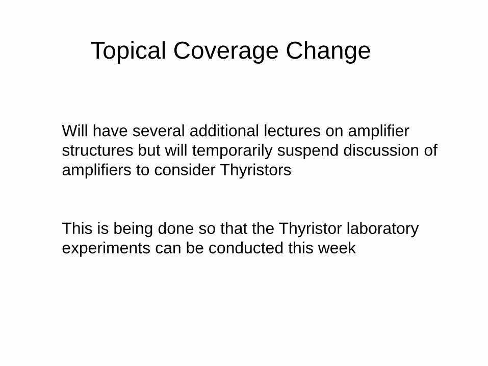
Topical Coverage Change
Will have several additional lectures on amplifier
structures but will temporarily suspend discussion of
amplifiers to consider Thyristors
This is being done so that the Thyristor laboratory
experiments can be conducted this week

Bipolar Processes• Comparison of MOS and Bipolar Process
• Parasitic Devices in CMOS Processes
• JFET
• Thyristors
SCR
TRIAC
Special Bipolar Processes
Outline

A-A’ Section
B-B’ Section
E
C
B
vertical npn
B
C
E
E
B
C
EC Blateral pnp
C B E B C E
Review from a Previous Lecture

A-A’ Section
B-B’ Section
GDS
S
D
G
p-channel JFET
Review from a Previous Lecture

BE
C
E
B
C
EC Blateral pnp
E
C
B
vertical npn
B
C
E
E C
B
Review from a Previous Lecture

L
G
DS
W
Resistor
Diode (capacitor)
GDS
S
D
G
p-channel JFET
Review from a Previous Lecture
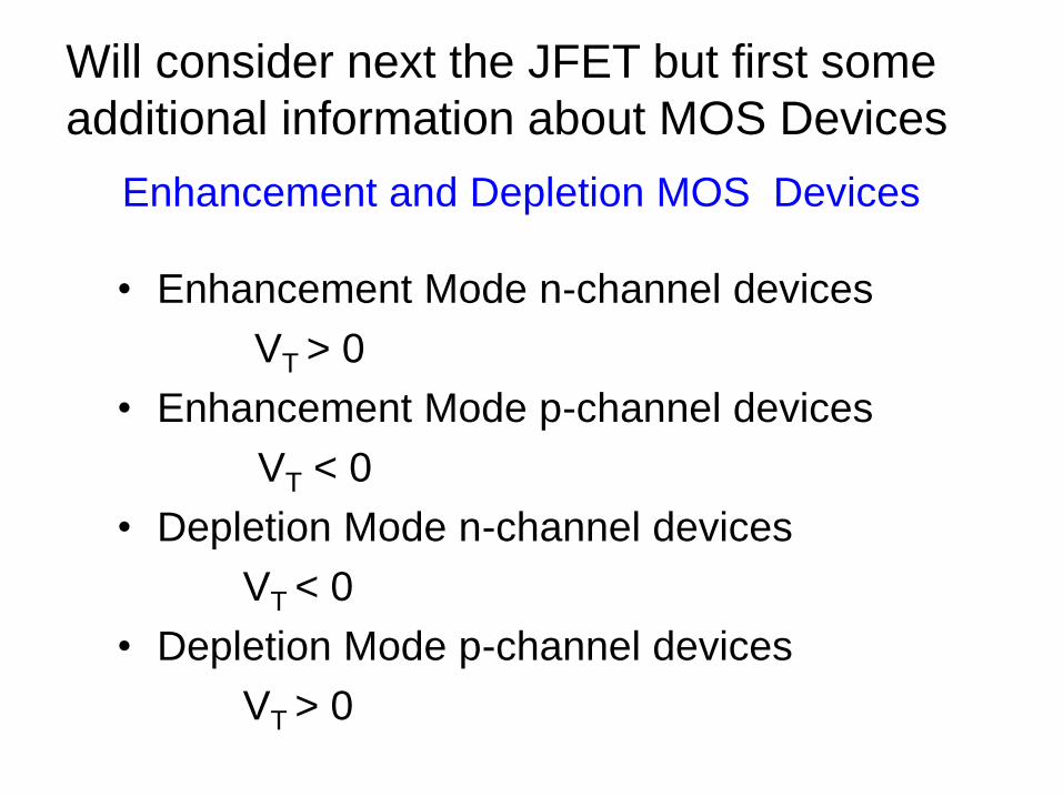
Enhancement and Depletion MOS Devices
• Enhancement Mode n-channel devices
VT > 0
• Enhancement Mode p-channel devices
VT < 0
• Depletion Mode n-channel devices
VT < 0
• Depletion Mode p-channel devices
VT > 0
Will consider next the JFET but first some
additional information about MOS Devices
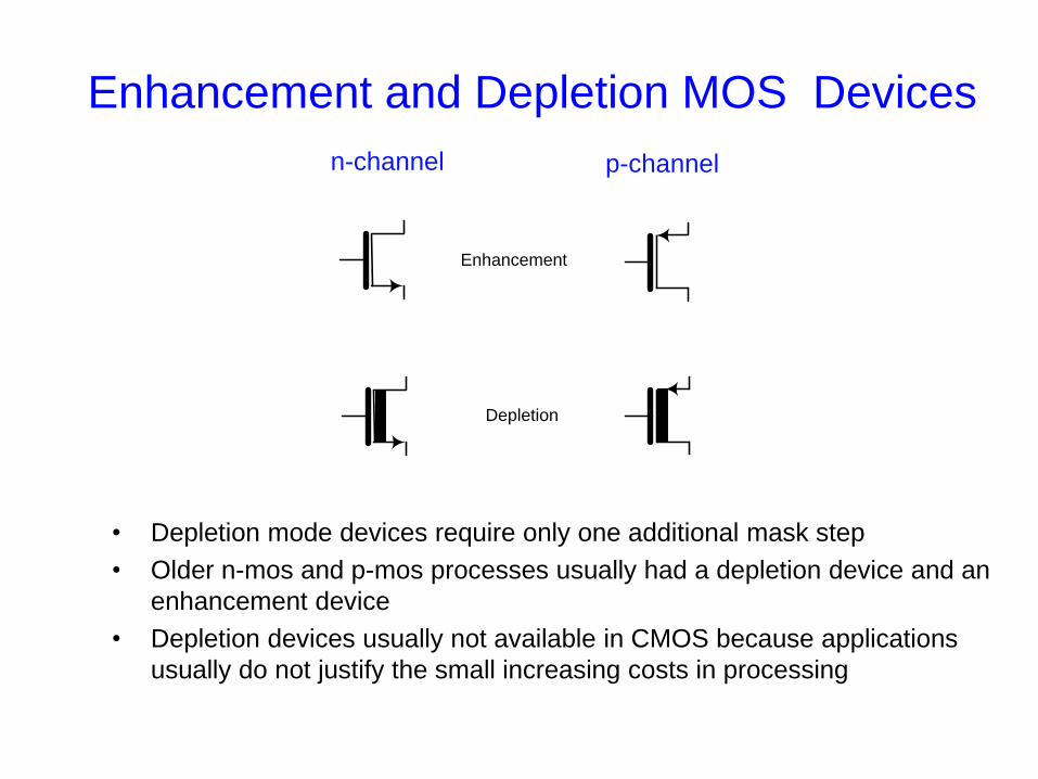
Enhancement and Depletion MOS Devices
• Depletion mode devices require only one additional mask step
• Older n-mos and p-mos processes usually had a depletion device and an
enhancement device
• Depletion devices usually not available in CMOS because applications
usually do not justify the small increasing costs in processing
n-channel p-channel
Enhancement
Depletion

The JFET
Under sufficiently large reverse bias (depletion region widens and channel
disappears - “pinches off”)
SD
G
SD
GWith VGS=0, channel exists under gate between D and S

The JFET
SD
G
SD
G
Under smaller reverse bias (depletion region widens and channel thins)

The JFET
Under small reverse bias and large negative VDS (channel pinches off)
SD
G
SD
G

The JFET
SD
G
0.3
0.3
GS P
DSSp DSD GS P DS GS P DS GS P2
P
2
GSDSSp GS P DS G
P
GS
S P
0 V V
2I VI V -V - V V V V > V -V
V 2
VI 1- V V V < V -V
V
V +0.3
D D
S S
G G
n-channel p-channelp-channel JFET
Square-law model of p-channel JFET
• Functionally identical to the square-law model of MOSFET
• Parameters IDSS and VP characterize the device
• IDSS proportional to W/L where W and L are width and length of n+ diff
• VP is negative for n-channel device, positive for p-channel device thus JFET is depletion mode device
• Must not forward bias GS junction by over about 300mV or excessive base current will flow (red constraint)
• Widely used as input stage for bipolar op amps
(IDSSp carries negative sign)

The JFET
0.3 0.3
0.3
GS P
DSS DSD GS P DS GS P DS GS P2
P
2
GSDSS GS P DS GS P
P
0 V V
2I VI V -V - V V V V < V -V
V 2
VI 1- V V V
V
> V -VV
GS
D D
S S
G G
n-channel p-channel
n-channel JFET
Square-law model of n-channel JFET
• Functionally identical to the square-law model of MOSFET
• Parameters IDSS and VP characterize the device
• IDSS proportional to W/L where W and L are width and length of n+ diff
• VP is negative for n-channel device, positive for p-channel device thus JFET is depletion mode device
• Must not forward bias GS junction by over about 300mV or excessive base current will flow (red constraint)
• Widely used as input stage for bipolar op amps
(not available in this process)
SD
G

The Schottky Diode
CA
• Metal-Semiconductor Junction
• One contact is ohmic, other is rectifying
• Not available in all processes
• Relatively inexpensive adder in some processes
• Lower cut-in voltage than pn junction diode
• High speed

The MESFET
SG
D
• Metal-Semiconductor Junction for Gate
• Drain and Source contacts ohmic, other is rectifying
• Usually not available in standard CMOS processes
• Must not forward bias very much
• Lower cut-in voltage than pn junction diode
• High speed

The Thyristor
S G D GSD
Consider a Bulk-CMOS Process
A bipolar device in CMOS Processes
p pn n
Have formed a lateral pnpn device !
Will spend some time studying pnpn devices

MOS and Bipolar Area Comparisions
How does the area required to realize a MOSFET
compare to that required to realize a BJT?
Will consider a minimum-sized device in both processes
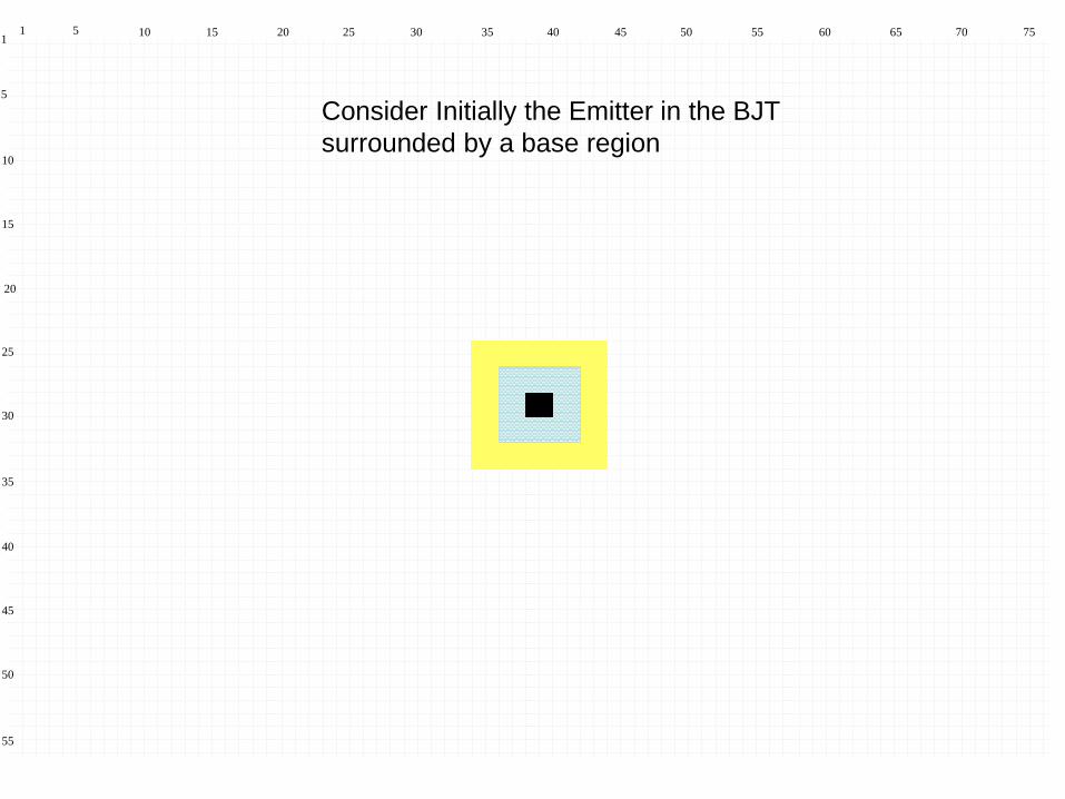
1 5 10 15 20 25 30 35 40 45 50 6055 7065 751
5
10
20
15
30
25
40
35
50
45
55
Consider Initially the Emitter in the BJT
surrounded by a base region


1 5 10 15 20 25 30 35 40 45 50 6055 7065 751
5
10
20
15
30
25
40
35
50
45
55
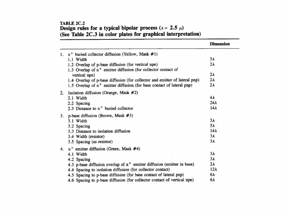
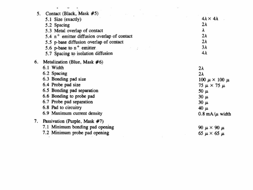
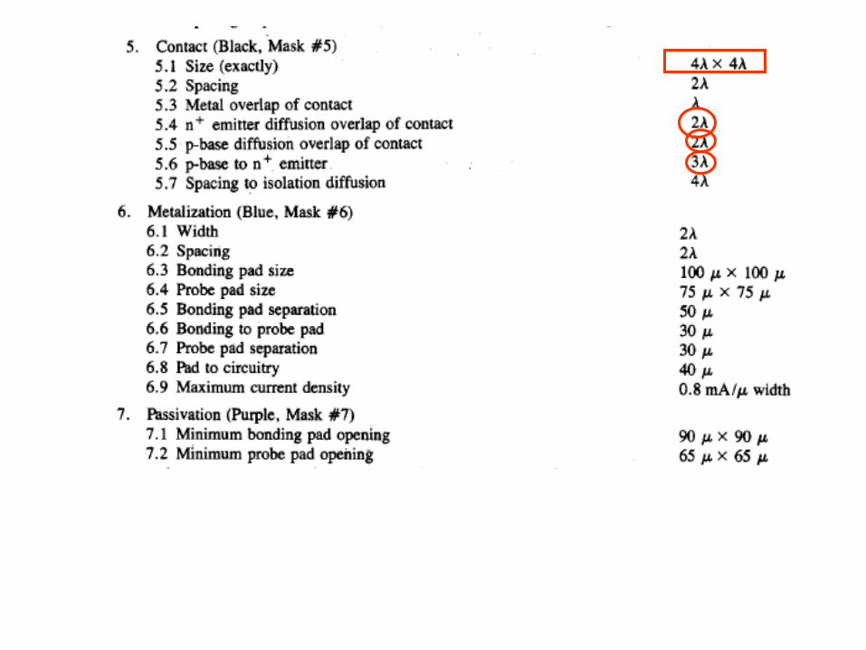
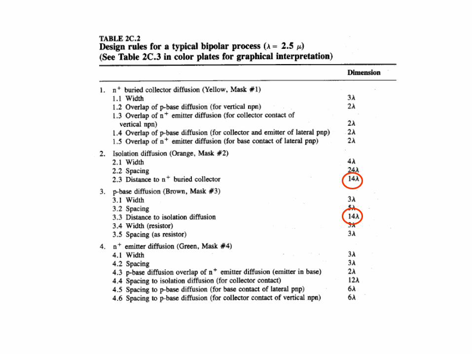
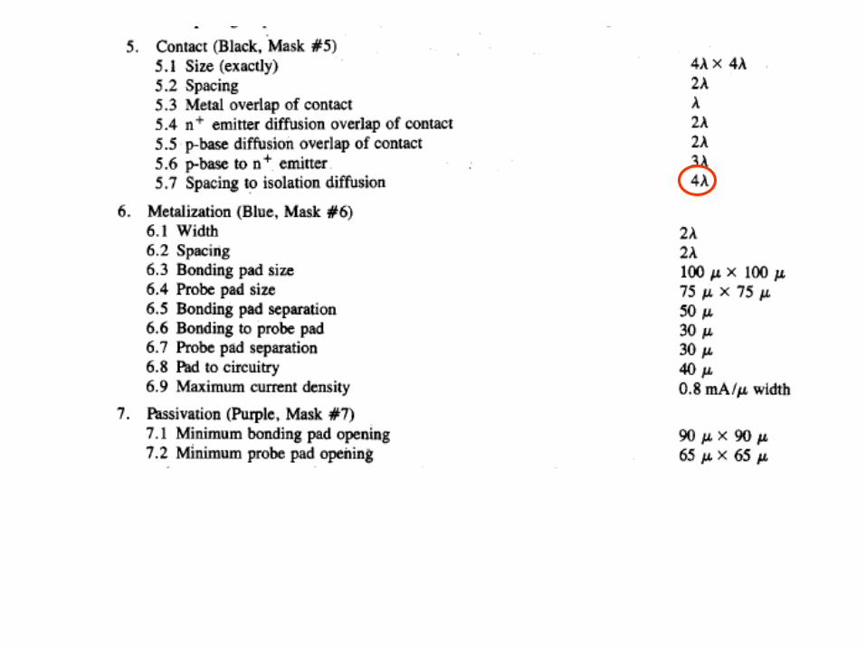
From design rules (left to right) 4.3, 5.1, 5.4, 5.6, 5.5
3
4
22
2
19
12

1 5 10 15 20 25 30 35 40 45 50 6055 7065 751
5
10
20
15
30
25
40
35
50
45
55
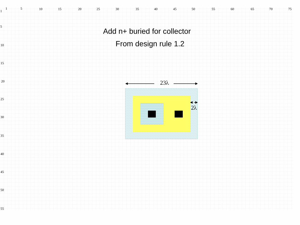
23
2
Add n+ buried for collector
From design rule 1.2

1 5 10 15 20 25 30 35 40 45 50 6055 7065 751
5
10
20
15
30
25
40
35
50
45
55
23
14 14
51
1414
Add n-epi region
from design rules 2.3 and 3.3
1 5 10 15 20 25 30 35 40 45 50 6055 7065 751
5
10
20
15
30
25
40
35
50
45
55
3 2
23
14
51
14
4
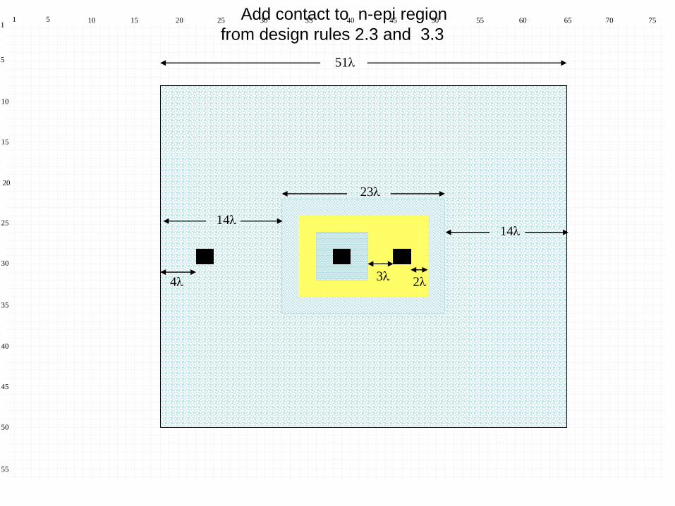
Add contact to n-epi region
from design rules 2.3 and 3.3


1 5 10 15 20 25 30 35 40 45 50 6055 7065 751
5
10
20
15
30
25
40
35
50
45
55
14
61
14
46
12
22
NOT TO
SCALENote: 26 required
Between p-base and
isolation diffusion
19
But, there are some rather strict rules relating to the epi contact
from (left to right) rules 4.4, 5.4, 4.6

1 5 10 15 20 25 30 35 40 45 50 6055 7065 751
5
10
20
15
30
25
40
35
50
45
55
26
71
6
12
2
2
Note: 26 required
Between p-base and
isolation diffusion
Note: Not to vertical Scale
44
19
14
Consider a structure with a collector contact on both sides of epi

1 5 10 15 20 25 30 35 40 45 50 6055 7065 751
5
10
20
15
30
25
40
35
50
45
55
26
71
6
12
2
Note: 26 required
Between p-base and
isolation diffusion
Note: Not to vertical Scale
44
4
19
26

1 5 10 15 20 25 30 35 40 45 50 6055 7065 751
5
10
20
15
30
25
40
35
50
45
55
71
Note: Not to vertical Scale
44
75
48

1 5 10 15 20 25 30 35 40 45 50 6055 7065 751
5
10
20
15
30
25
40
35
50
45
55
Note: Not to vertical Scale
75
48
Bounding Area = 36002
Major contributor to large size of BJT is the isolation diffusion which diffuses
laterally a large distance beyond the drawn edges of the isolation mask

1 5 10 15 20 25 30 35 40 45 50 6055 7065 751
5
10
20
15
30
25
40
35
50
45
55
16
13
Bounding Area = 2082
Comparison with Area for
n-channel MOSFET in Bulk CMOS

1 5 10 15 20 25 30 35 40 45 50 6055 7065 751
5
10
20
15
30
25
40
35
50
45
55
14
12
Bounding Area = 1682
Active Area = 62
Minimum-Sized MOSFET

1 5 10 15 20 25 30 35 40 45 50 6055 7065 751
5
10
20
15
30
25
40
35
50
45
55
Note: Not to vertical Scale
75
48
MOSFET BJT

Area Comparison between
BJT and MOSFET
• BJT Area = 3600 2
• n-channel MOSFET Area = 168 2
• Area Ratio = 21:1

Two-Port Amplifier Models
Bipolar Processes• Comparison of MOS and Bipolar Process
• Parasitic Devices in CMOS Processes
• JFET
• Thyristors
SCR
TRIAC
Special Bipolar Processes
Outline

Thyristors
The good and the bad!

Thyristors
The good
SCRs
Triacs
The bad
Parasitic Device that can destroy integrated circuits

The SCR
Silicon Controlled Rectifier
• Widely used to switch large resistive or inductive loads
• Widely used in the power electronics field
• Widely used in consumer electronic to interface between logic and power
Anode
Cathode
GateG
C
A
p
p
n
nG G G
A A A
C C C
Symbols
Consider first how this 4-layer 3-junction device operates
Usually made by diffusions in silicon

Operation of the SCR
C
G
A
Q1
Q2
IF
IG
IC1
IB2
IC2
IB1
G
C
A
p
p
n
n
GC
A
p
n
n
p
n
p
C1
B1
E1
C2
B2
E2
G
A
C
VF
VG
IF
IG
Not actually separated but useful for describing operation

Variation of Current Gain (β) with Bias for BJT
Note that current gain gets very small at low base current levels

Operation of the SCR
C
G
A
Q1
Q2
IF
IG
IC1
IB2
IC2
IB1
GC
A
p
n
n
p
n
p
C1
B1
E1
C2
B2
E2
Consider a small positive bias (voltage or current) on the gate (VGC<0.5V) and a positive
and large voltage VF
Will have C1 FV V - 0.5V
Thus Q1 has a large positive voltage on its collector
Since VBE1 is small, IC1 will be small as will IC2 so diode equation governs BE junction of Q1
IF will be very small
G
C
A
VF
IG
IG
IF
p
p
n
n

Operation of the SCR
C
G
A
Q1
Q2
IF
IG
IC1
IB2
IC2
IB1
GC
A
p
n
n
p
n
p
C1
B1
E1
C2
B2
E2
Now let bias on the gate increase (VGC around 0.6V) so Q1 and Q2 in FA
From diode equation, base voltage VBE1 will increase and collector current IC1 will increase
C1 FV V - 0.5V
Thus base current IB2 will increase as will the collector current of IC2
B1 G 1 2 B1I = I + β β I
Under assumption of operation in FA region get expression
This is regenerative feedback (actually can show pole in RHP)
G
C
A
VF
IG
IG
IF
p
p
n
n

Very Approximate Analysis Showing RHP Pole
GC
A
p
n
n
p
n
p
C1
B1
E1
C2
B2
E2
G
A
Q1
Q2
IF
IG
IC1
IB2
IC2
IB1
VGVCC
C
VF
RL
IGCB
1 2
2 1 2 1
1
G B B C G
C B
B BE G
V sC I I I
I I
I R V
1 21
BEG G
BE B
RV I
sR C
1 2 1
BE B
pR C

Operation of the SCR
GC
A
p
n
n
p
n
p
C1
B1
E1
C2
B2
E2
C1 FV V - 0.6V
B1 G 1 2 B1I = I + β β I
Under assumption of operation in FA region get expression
What will happen with this is regenerative feedback?
IC1 will continue to increase and drive Q1 into SAT
If IG larger but less than , it can be removed and current
will continue to flow
This will try to drive VA towards 0.9V (but forced to be VF!)
The current in VF will go towards ∞
The SCR will self-destruct because of excessive heating !
Too bad the circuit self-destructed because the small gate current was able to
control a lot of current!
G
A
Q1
Q2
IF
IG
IC1
IB2
IC2
IB1
IGC
VF
If IG is small (and thus β1 and β2 are small) IF will be very small
1 2 B1β β I

Operation of the SCR
Consider a modified application by adding a load (depicted as RL)
G
C
A
VF
VG
IG
IF
p
p
n
n
VCC
RL
All operation is as before, but now, after the triggering occurs, the voltage VF will
drop to approximately 0.8 V and the voltage VCC-.8 will appear across RL
If VCC is very large, the SCR has effectively served as a switch putting VCC
across the load and after triggering occurs, IG can be removed!
But, how can we turn it off? Will discuss that later
G
A
Q1
Q2
IF
IG
IC1
IB2
IC2
IB1
VGVCC
C
VF
RL
IG

Operation of the SCR
The Ideal SCR Model
G
A
C
VF
VG
IF
IG
As for MOSFET, Diode, and BJT, several models for SCR can be developed
1
2
,F F G
G G
I f V V
I f V
1 ,F I F GI f V I 1 ,F IA F GI f V Vor
SCR model
2G I GI f V 2G I GI f V
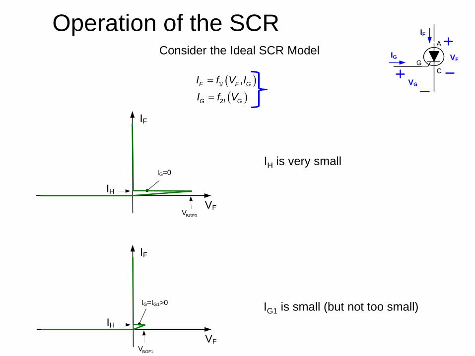
Operation of the SCR
IF
VF
IG=0
BGF1 V
IH
IF
VF
IG=IG1>0
BGF0 V
IH
Consider the Ideal SCR ModelG
A
C
VF
VG
IF
IG
IH is very small
1 ,F I F GI f V I
2G I GI f V
IG1 is small (but not too small)

Operation of the SCR
Operation with the Ideal SCR
VCC
VG
RL
VFIF
IGCC F L FV = I R +VLoad Line:
IF
VF
IG=0
CC V
CC
L
V
R
Load
Line
IH
The solution of these two equations is at the intersection of
the load line and the device characteristics
Analysis:CC F L FV = I R +V
when IG=0
Note three intersection points
Two (upper and lower) are stable equilibrium
points, one is not
When operating at upper point, VF=0 so VCC
appears across RL We say SCR is ON
When operating at lower point, IF approx 0 so
no signal across RL We say SCR is OFF
When IG=0, will stay in whatever state it was in
1 ,F I F GI f V I
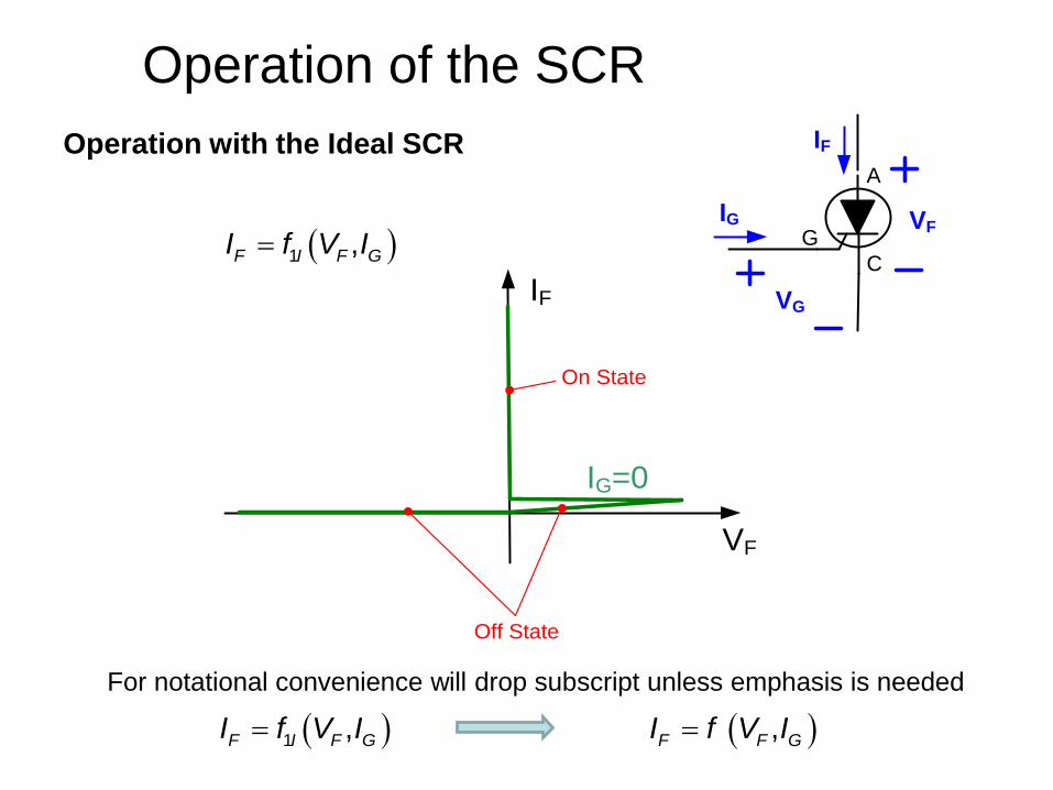
Operation of the SCR
Operation with the Ideal SCR
IF
VF
Off State
On State
IG=0
G
A
C
VF
VG
IF
IG
1 ,F I F GI f V I
1 ,F I F GI f V I ,F F GI f V I
For notational convenience will drop subscript unless emphasis is needed

Operation of the SCR
Operation with the Ideal SCR
IF
VF
IG=0
CC V
CC
L
V
R
Load
Line
IH
Now assume it was initially in the OFF state and then
a gate current was applied
CC F L FV = I R +V
Now there is a single intersection point so a
unique solution
The SCR is now ON
IF
VFCC V
CC
L
V
R
Load
Line
IH
IG=IG1>0
Removing the gate current will return to the
previous solution (which has 3 intersection points) but it
will remain in the ON state
,F F GI f V I
VCC
VG
RL
VFIF
IG

Operation of the SCR
Operation with the Ideal SCR
Turning SCR off when IG=0
Reduce VCC so that VCC/RL goes below IH
This will provide a single intersection point
VCC can then be increased again and SCR will stay off
Must not increase VCC much above VBGF0 else will turn on
IF
VF
IG=0
CC V
CC
L
V
R
Load
Line
IH
BGF0 V
VCC
VG
RL
VFIF
IG

Operation of the SCR
Operation with the Ideal SCR
Turning SCR off when IG=0
IF
VF
IG=0
CC V
CC
L
V
R
Load
Line
IH
BGF0 V
VCC
VG
RL
VFIF
IG

Operation of the SCR
Operation with the Ideal SCR
Often VCC is an AC signal (often 110V)
SCR will turn off whenever AC signal goes negative
IF
VF
IG=0
CC V
CC
L
V
R
Load
Line
IH
BGF0 V
CC
L
V
R
VCC
VG
RL
VFIF
IG

Operation of the SCR
Operation with the Ideal SCR
Often VCC is an AC signal (often 110V)
SCR will turn off whenever AC signal goes negative
IF
VF
IG=0
CC V
CC
L
V
R
Load
Line
IH
BGF0 V
CC
L
V
R
VCC
VG
RL
VFIF
IG

Operation of the SCR
Operation with the Ideal SCR
Turning SCR off when IG>0
Reduce VCC so that VCC/RL goes below IH
This will provide a single intersection point
But when VCC is then increased SCR will again turn on
Will not turn off if IG is very large
IF
VFCC V
CC
L
V
R
Load
Line
IH
IG=IG1>0
CC
L
V
R
VCC
VG
RL
VFIF
IG

End of Lecture 29


![EE330 Laboratory Experiment No. 7 N-MOSFET Current Mirrors · EE330 Laboratory Experiment No. 7 N-MOSFET Current Mirrors [Reference: Chapter 8 of Sedra & Smith, 7th ed.; pp. 512-517]](https://img.pdfslide.us/doc/110x75/5eb9e8bcd5eebf230573987e/ee330-laboratory-experiment-no-7-n-mosfet-current-mirrors-ee330-laboratory-experiment.jpg)