Embed Size (px)
Citation preview

TOP-LEVEL VERILOG MODEL
FOR A SERIAL TRANSCEIVER
by
UDAYKARAN R. TUMMALA, B.E.
A THESIS
IN
ELECTRICAL ENGINEERING
Submitted to the Graduate Faculty
of Texas Tech University in Partial Fulfillment of the Requirements for
the Degree of
MASTER OF SCIENCE
IN
ELECTRICAL ENGINEERING
Approved
December, 2001

ACKNOWLEDGEMENTS
I want to express my gratitude to my advisor, Dr. Micheal E Parten, Professor,
Department of Computer and Electrical Engineering, Texas Tech University for his
continued guidance and support during the preparation of this dissertation. Dr. Parten's
recommendations through out the work were truly invaluable. Many thanks to Dr. Jon G.
Bredeson, Professor and Chairman, Department of Computer and Electrical Engineering,
Texas Tech University for his time as a member of my thesis committee. Many thanks to
Dr. Ronald H.Cox for his valuable suggestions. I would like to thank Bob Payne, Design
Manager, Wizard group, Texas Instmments for the opportunity and guidance given to me
regarding this project. My special thanks go to Roger Chan who had been a great mentor
for me throughout this work. I am also very thankful to Doug Wente, John Powers and
Wahed for their help.
Words cannot tmly express my deepest gratitude and appreciation to my parents
and sister who always gave me their love and emotional support. Without them, I could
not have come this far in my life.
Finally, I would like to thank all my friends who gave their valuable insights and
suggestions.
11

TABLE OF CONTENTS
ACKNOWLEDGEMENTS n
LIST OF TABLES vi
LISTOFHGURES vn
CliAPTER
L INTRODUCTION 1
1.1 Functional verification of IC's 1
1.2 Hardware Simulation 2
1.3 Serial Transceiver 3
1.4 Verification of Transceiver 4
1.5 Thesis Organization 4
IL SERIAL TRANSCEIVER 6
2.1 Functionality of Transceiver 6
2.2 Individual channel overview 8
2.3 Serializer and Deserializer 9
2.4 8B/10B Encoder/Decoder 10
2.5 PRBS Generation and Verification 12
m. BEHAVIORAL MODELLING 14
3.1 Top level model 14
3.2 Behavioral models 13
3.3 Code Structure 16
111
3.3.1 Declaration Statements 16
3.3.2 Concurrent Statement 17
3.3.3 Sequential Statements 17
3.4 Verilog Operators 17
3.5 Common models 20
3.6 ASIC libraries 31
3.7 Net list from schematic 32
IV. TEST BENCHES 34
4.1 HDL Test Bench 34
4.2 Transceiver instantiation 36
4.3 Master file 37
4.4 Clock set-up 38
4.5 Top-level simulation plan 39
V. AT-SPEED VERIFICATION 41
5.1 PRBS Testing 41
5.1.1 PRBS External mode 41
5.1.2 PRBS Intemal mode 43
5.2 PRBSPOWER Test mode 44
5.3 SERDES Test Mode 46
5.3.1 EN/DEC Off 47
5.3.2 SERDES with EN/DEC on 50
5.4 10 GIG Mode.... 51
iv

5.5 ASYNC Test mode 54
VL CONCLUSION 58
REFERENCES 60
LIST OF TABLES
2.1 Valid K-characters 11
3.1 Verilog HDL Operators 18
5.1 Encoded K-characters 48
VI
LIST OF FIGURES
1.1 Hardware simulation 2
2.1 High-level block diagram of serial transceiver 7
2.2 Block diagram of individual channel 9
3.1 Module specifications 15
3.2 Circuit of module TXBU 20
3.3 Module PASSMUXSET 22
3.4 Module CBSWITCH 24
3.5 Module NO410 25
3.6 D flip-flop 27
3.7 Module INBUF_3VTOL 29
3.8 Test Enable mode circuit 30
4.1 Test Fixture 34
4.2 Master file 37
4.3 Top-level simulation plan 40
5.1 Simulations results for PRBS extemal testing 42
5.2 Simulation results for PRBS intemal testing 44
5.3 Input signals for PRBSPOWER test 45
5.4 Simulation results of PRBSPOWER test 46
5.5 SERDES with EN/DEC off test results 50
5.6 Results of SERDES test with EN/DEC on 51
Vll

5.7 Inputs for lOGig test mode 52
5.8 10 Gig mode outputs 53
5.9 Transceiver instantiation 54
5.10 ASYNC test results 57
Vll l

CHAPTER I
INTRODUCTION
1.1 Functional verification of IC's
In today's worid of multi million gate IC's, functional verification continues to be
major bottieneck in releasing a chip for production. The purpose of functional
verification is to identify defects in the design of a chip that cause its behavior to deviate
from what is permitted by specification. The more complex the design is, the greater the
chance that some parts of system will not function property together or will not function
in all cases. One of the most effective ways to verify that a design functions correctly is
through the use of behavioral modehng. Circuit level simulation is too slow to be used for
the functional verification of large circuits. For most designers, the perfect design tool
would be a SPICE (Simulation Program with Integrated Circuit Emphasis) simulator with
infinite speed and design capacity. However, speed and capacity limitations mean
excessive mntimes and insufficient functional coverage. As a result, it is often necessary
to migrate to HDL (Hardware descriptive language) to complete verification. Even after
migrating to HDL- verification, it is not feasible to test the complete chip at gate level, as
it is a time consuming process. The viable alternative is simulating at the logic level
instead of circuit level(transistor level or gate level). Using a HDL, like verilog it is
possible to write behavioral models of the sub blocks in the design and simulate the
complete design by test benches written in the same HDL.

This approach to functional verification makes possible simulation of large and very
large circuits such as a serial transceiver. Behavioral models can speed up the simulation
by the factor of 10 to 100 times depending upon the level of the behavioral modeling.
1.2 Hardware simulation
Hardware description languages are modeling tools for creating a hardware
model. The top-level model may be developed for different applications. One such
application is simulation. Simulation is the act of exercising a model of an actual
component in order to verify its conduct or functions under a given set of conditions.
In the hardware design environment, a hardware description uses component
models and definitions from a simulation library (ASIC libraries) to form a simulatable
hardware model. As shown in Figure 1.1, the hardware models, the models for library
elements, a test bench enclosing the model that is being simulated and a set of stimuli are
used as inputs to a hardware simulation engine.
The simulator produces simulation results that are indicative of the conduct of the
hardware component for the given set of test data. Once the desired function is verified
the simulation results can be used to generate test vectors, which are used to test the
physical device. The output generated by the simulator depends on the level of detail of
the hardware model presented to it. A simulator based on a hardware description
language can process hardware details supported by its input HDL.

Top-level Hardware Description model (Verilog)
Component library (ASIC models)
Test bench Specification
Simulation Engine (Verilog-XL)
Figure 1.1 Hardware simulation'
Simulation Results (Output)
Test vector Generation
1.3 Serial Transceiver
Transceivers are one of the most important components in present networking
age. These devices can dehver high-speed bi-directional point-to-point data transmission
up-to lOGbps of data transmission capacity. The primary application of this device is to
provide a building block for developing point-to-point base band data transmission over
controlled impedance media. This device performs parallel-to-serial, serial-to-parallel
conversion and clock extraction functions for a physical layer interface. This device
consists of four channels with a selectable synchronized or independent channel
operation function. It also has selectable transmit only, receive only, or transceiver

functions. Some of the important parts in this transceiver are serializer, deserializer,
encoder, decoder, PRBS generation and verification unit, and clock synthesizer.
1.4 Verification of transceiver
For a large design with extensive functionality, complete functional verification
at transistor or gate level is a time consuming process. The best way to verify the
complete chip is by generating the top-level model of the design and testing with
different test benches. The top-level model is generated by extracting the net list of the
design. The net list contains behavioral models that are written for different blocks, thus
reducing the amount of gate level or transistor level net list. This top level combined with
the ASIC library models and test bench can be simulated by the simulator, verilog-XL,
and the results generated. Different test benches can be used to test different
functionahties of the device. The objective of this thesis is to develop a top-level verilog
model of a chip having a large and complex design to verify the complete functionality of
that particular chip. A serial transceiver, a large design, will be verified using this
procedure.
1.5 Thesis Organization
This thesis is organized in a way to explain the procedure of developing a top-
level verilog model for the transceiver and different test benches to verify the
functionality of the transceiver. Behavioral models for sub blocks along with schematics
are presented in the thesis to explain the procedures followed in developing the model.
Simulation results will be presented for better understanding of the functions of the
4

device and the test benches used for verification. Chapter 11 focuses on the features of
the serial transceiver. Chapters III to V describe different stages of the verification using
the top-level verilog HDL model including the generation of the model. Chapter VI gives
the conclusion to the project, which shows how effective this approach is for the
functional verification of such a large design.

CHAPTER n
SERIAL TRANSCEFVER
2.1 Functionahty of Transceiver
To understand how to develop the top-level model and different test benches, the
functionality of the transceiver must be discussed. Some of the standard features and
functions are given in IEEE Draft P802.3ae. This device is a four-channel serial back
plane transceiver, delivering high-speed bi-directional point-to-point data transmissions
to provide up to lOGbps of data transmission capacity. The main features of this device
are given in "TLK Cell overview" document of Texas Instmments. This device provides
very high speed VO data channels for point-to-point base band data transmission over
controlled impedance media of approximately 50 Q. The transmission media can be a
printed-circuit board, copper cable, or fiber-optic cable. The device can also be used to
replace parallel data transmission architectures by providing a reduction in the number of
traces, connector pins, and transmit/receive pins. Parallel data loaded into the transmitter
is dehvered to the receiver over a serial channel, which can be a coaxial cable, a
controlled impedance back plane, or an optical link. It is then reconstructed into its
original parallel format. Some of the standard features of this device are mentioned in
IEEE Draft P802.3ae/D2.1. This draft contains Media Access Control (MAC) parameters,
physical layer, and management parameters for 10 Gb/s operation.
This device performs the parallel-to-serial, serial-to-parallel conversion, and clock
extraction functions for a physical layer interface. It also provides a selectable 8b/10b
encode/decode function. The four transceivers in the device can be configured as either

four separate links, or synchronized together as single data path. The block diagram of
such a device is shown in Figure 2.1. This diagram provides a high level description of
the device.
JRDA(0:9) IICA
'4 •
JvIFA TDA(0:9)
RDB(0:9) M JLCB
MFB
TDB(0:9)
RDC(0:9)
RCC
MFC
TDC(0:9)
RDD(0:9)
RCD
MFD
TDD(0:9)
RFCP/RFCN
RDO-9 TX+ RCLK TX-
Channel A MFA RX+
RX-TDO-9
RFFCTX
t RDO-9 TX+ RCLK TX-
Channel B MFB
RX+ RX-
TDO-9 REFCLK
t RDO-9 TX+ RCLK TX-
Channel C MFC RX+
RX-TDO-9 REFCLK
t RDO-9 TX+
TX-RCLK
Channel D MFD RX+
RX-TDO-9 REFCLK
A
TXAP TXAN^
— w RXAP
^
^ ^
RXAN
TXBP
r TXBN • RXBP
^
RXBN ^
^
TXCF
TXCN
^
^ ^
RXCP
RXCN
TXDP TXDN •"
^ RXDP
^
^ ^ RXDN
Figure 2.1. High-level block diagram of serial transceiver
7

Each block acts as an individual transceiver and all four channels can be
synchronized through an extemal pin. When this extemal pin is 0, the device is in
independent channel mode and when it is 1 it is in the in channel sync mode, i.e., all the
four channels are synchronized and device will act as 10 Gigabit transceiver.
2.2 Individual channel overview
Some of the important blocks of each individual channel are the serializer, deserializer,
clock synthesizer, clock recovery, PRBS generator and verification unit, encoder, decoder
and comma detect circuit. Figure 2.2 gives a block diagram description of each channel
core.
8

Parallel Tx 8B/10B Encoder A
PRBS Generator
RFCN/RFCP
Parallel Rx Decoder
Parallel to serial
Clock synthesizer (PEL)
i Clock recovery
Serial to parallel & Comma detect
Figure 2.2 Block diagram of individual channel
Rx
2.3 Serializer and Deserializer
The serializer on each channel takes in 10 bit wide data from either the 8B/10B
encoders, if enabled, or directly from the transmit data bus and converts it to a serial
stream. It shifts out the 10 bits 1 bit at a time. The deserializer is the in\ erse function of
the serializer. The function of this block is to perform the conversion from senal data to
parallel data. For each channel serial data is received on the RXxp, RXxn pins. The
interpolator and clock recovery circuit locks to the data stream. The recovered clock is
used to retime the input data stream. If enabled, the 10 bit wide parallel data is then fed
into 8B/10B decoders. The serialization and deserialization is controlled with an extemal
pin CODE. When the CODE pin is asserted the on chip encoders and decoders are
enabled. When it is not asserted, the device performs seriahzation and deserialization.
2.4 8B/10B Encoder/Decoder
This device uses an 8B/1 OB-encoding algorithm in order to provide good
transition density for clock recovery and error checking. Arbitrary data patterns may not
be suitable for serial transmitter and receiver as it results in long mns of I's and O's.
Because of this the receiver recovery cannot lock onto long mn length. In order to
counter this problem each byte (8 bit word) is encoded as a lObit word. This transmission
code includes D-characters, used for transmitting, and K-characters, used for transmitting
protocol information. These K and D characters are nothing but a unique pattern of I's
and O's that either cannot occur as part of valid data or is a pattern that repeats at defined
intervals. Each K or D character code word can also have both positive and a negative
parity version. The parity of a code word is selected by the encoder to balance the
mnning disparity of the serialized data stream.
The generation of K-characters is controlled by TDx8 pin. when this pin is
asserted along with the 8 bits of dataTDx [0.... 7], an 8b/10b K-character is transmitted.
10
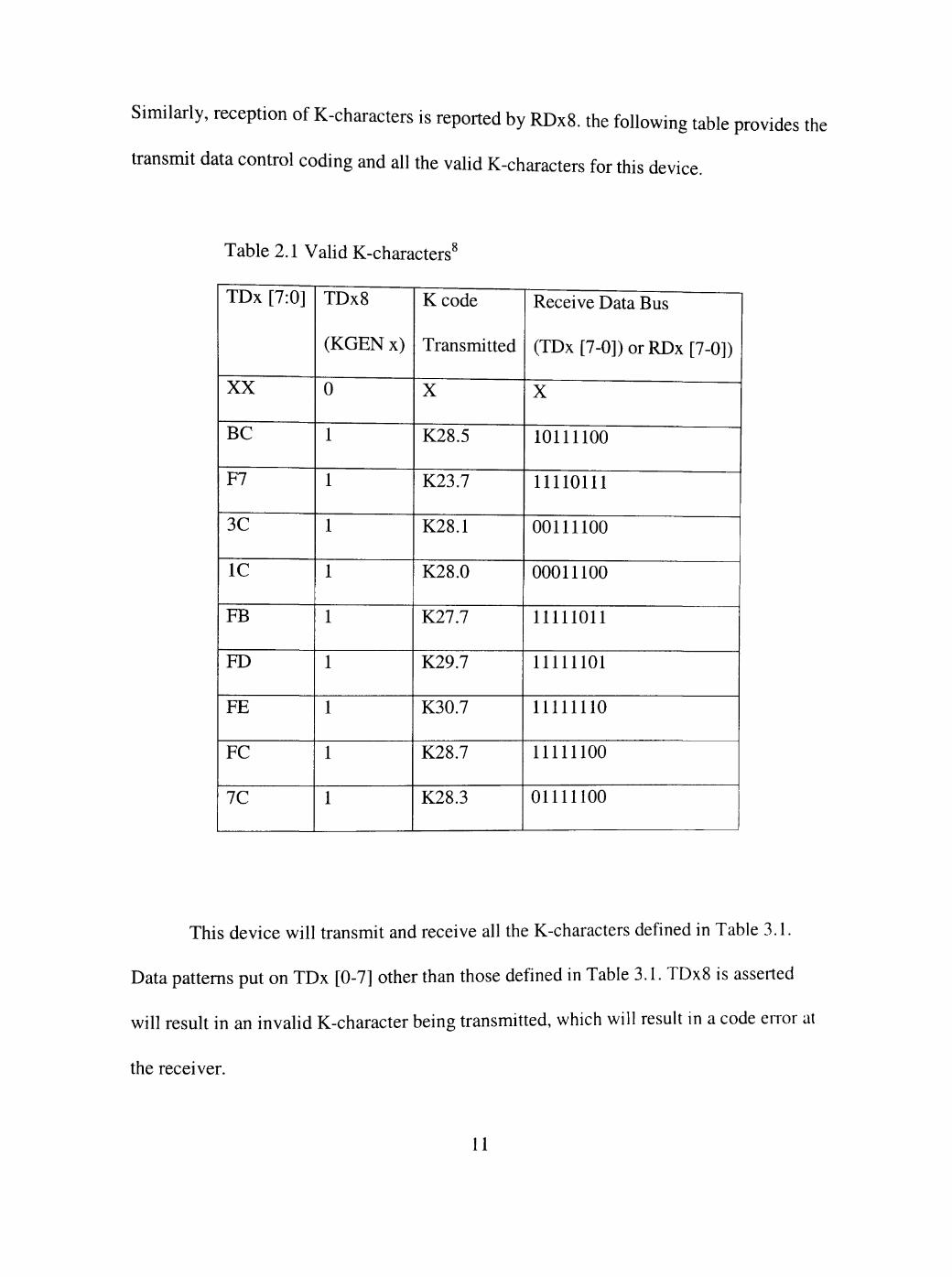
Similarly, reception of K-characters is reported by RDx8. the following table provides the
transmit data control coding and all the valid K-characters for this device.
Table 2.1 Vahd K-characters^
TDx [7:01
XX
BC
F7
3C
IC
FB
ED
FE
EC
7C
TDx8
(KGEN x)
0
1
1
1
1
1
1
1
1
1
Kcode
Transmitted
X
K28.5
K23.7
K28.1
K28.0
K27.7
K29.7
K30.7
K28.7
K28.3
Receive Data Bus
(TDx [7-0]) or RDx [7-0])
X
10111100
11110111
00111100
00011100
union
11111101
11111110
11111100
01111100
This device will transmit and receive all the K-characters defined in Table 3.1.
Data pattems put on TDx [0-7] other than those defined in Table 3.1. TDx8 is asserted
will result in an invalid K-character being transmitted, which will result in a code error at
the receiver.
11
For each channel, the 8B/10B decoder converts lObit-encoded data back into
8bits. There is a comma detect circuit to provide for byte synchronization to an 8B/10B
transmission code. The reception of K-characters is reported by the assertion of RDx (K
flag) on each channel. Decoder error output may be indicated if there is a disparity error
or error propagation code. When a decoder error is detected all I's are placed on the
receive data bus for that channel.
2.5 PRBS Generation and Verification
This device has a built-in 2^ -1 PRBS (Pseudo Random Bit Stream) self test
function available on each channel. This function can be enabled through an extemal pin
PRBSEN. When enabled, a PRBS pattern is generated and is supplied to the serializer.
Data from the normal input source is ignored during the self-test mode. The PRBS
pattem is then fed through the transmit circuitry as if it were normal data and sent out to
the transmitter. This pattem can be looped back to the deserializer and PRBS verifier
watches the deserialized data from the deserializer. This pattem is compared against
known PRBS data and if a bit or more does not match, an error is signaled on the receive
channel's multi-function (MFx) pin.
In addition some of the other important blocks are clock synthesizer and clock
recovery. On chip PLL's are used to provide high-speed clocks and these clocks are used
to lock the receiver data stream. There are also has three operational configurations
controlled by two configuration pins, CONFIGO and CONFIGl. When both are 0, the
device is in Full Duplex Transceiver mode. When CONFIGO is 0 and CONFIG I is 1, the
12

device is in the transmit only mode. When 1 and 0, the device is in the receive only
mode. The device has a comprehensive suite of built-in-self tests. The loop back function
provides for at-speed testing of transmit/receive portions of the circuitry. It can provide a
self-test function by enabling the intemal loop-back path with the assertion of the LPENx
pin for each channel. Enabling this pin will cause serial transmitted data to be routed
intemally to the receiver for that channel. The parallel data output can be compared to the
parallel input data for that channel to provide functional verification.
13

CHAPTER m
BEHAVIORAL MODELLING
3.1 Top level model
The first step in the functional verification of the device is to create a top-level
hardware description model. The level of abstraction for modeling a circuit depends on
the purpose for which the model is intended. If the model is used to verify the
functionality of circuit, a very abstract behavioral model is necessary. The behavioral
level of abstraction is most appropriate for verification and functional simulation of
complex hardware units. But creating a single behavioral model for such a large design,
which includes lot of blocks and features is not feasible. This problem is countered by
describing individual smaller modules in verilog HDL. Using verilog HDL, behavioral
models of different modules can be written and these models can be extracted in a top-
level net list extraction.
By creating behavioral models of different blocks the overall net list can be
minimized. This is possible because the extraction will not go deep into the block once
there is a behavioral model. Also the block, which has a behavioral model, can be used
multiple times and be only one module in the entire net list. Writing behavioral models
for some analog blocks is very important. These blocks will not have any influence on the
overall functionality as they are used for intemal signal modifications. For these blocks
the output is equal to the input. So instead of dumping out the transistor level net list it is
necessary to create a behavioral model. This results in a reduction of overall net list si/c.
14

which in tum reduces verification time. In this chapter, how the behavioral models are
created using verilog HDL will be explained with some examples.
3.2 Behavioral models
A behavioral model of a module is an abstraction of how the module works. The
outputs of the module are described in relation to its inputs. Verilog HDL is used to
describe hardware modules. The main component of the language is a module. As shown
in Figure 3.1, a module description consists of the keyword module, the name of the
module, a list of ports of the hardware module, the module functionality specification,
and the keyword endmodule.
module module name
List of ports;
Declarations;
Specification of the functionality of module;
endmodule
Figure 3.1 Module specifications'
15
As in many software languages, there is usually more than one way in which a
module can be described in verilog HDL. Various descriptions of a component may
correspond to descriptions at various levels of abstraction or to various levels of detail of
the functionality of a module. One module description may be at the behavioral level of
abstraction with no timing details, while another description for the same component may
include transistor-level timing details. There is no need for transistor-level timing details
for functional verification. So, the module will be described at the behavioral level of
abstraction. Also, a module may be part of a library of predesigned library components
and include detailed timing and loading information.
3.3 Code Stmcture
Behavioral modeling in verilog HDL is described by specifying a set of
concurrently active procedural blocks in a high-level programming language that together
describe the operation of the system. High-level programming language constructs are
available in verilog for behavioral modeling. Different types of statements that are used
in behavioral modeling are discussed below.
3.3.1 Declaration Statements
These statements declare objects for use in concurrent and sequential statements.
In a Verilog design unit, a module statement does not need to be declared; nor do
subprograms, that is, a task or function. There is no dedicated declarative region in a
module, sequential block, concurrent block, task or function.
16
3.3.2 Concurrent Statement
These are statements that are executed in parallel. They operate independently of
all other concurrent statements. When modeling hardware stmcture they represent
independent sections of the circuit being modeled. Each concurrent statement is executed
asynchronously with all other concurrent statement. The continuous assignment and
always statement are concurrent. A continuous assignment uses the reserved word assign-
to-assign data objects of any of the net data types. A task cannot be called concurrently.
3.3.3 Sequential Statements
Sequential statements are statements that are executed depending upon the
procedural flow of constructs that surround them. Sequential statements reside in an
always statement, that may, or may not, contain sequential begin-end procedural blocks.
The assigned objects are of type reg or integer.
3.4 Verilog Operators
Verilog HDL operators perform an operation on one or more operands within an
expression. An expression combines operands with appropriate operators to produce the
desired functional expression. Table 3.1 shows the operators in descending order of
precedence. Operators with equal precedence are shown grouped.
17

Table 3.1 Verilog HDL Operators^
Verilog Operator
[]
( )
1
~
&
1
- &
~i A
~A Qj. A..
+
-
{ }
{{}}
*
/
%
Name
bit-select or part-select
parenthesis
logical negation
negation
reduction AND
reduction OR
reduction NAND
reduction NOR
reduction XOR
reduction XNOR
unary (sign) plus
unary (sign) minus
concatenation
replication
multiply
divide
modulus
Functional Group
logical
bit-wise
reduction
reduction
reduction
reduction
reduction
reduction
arithmetic
arithmetic
concatenation
replication
arithmetic
arithmetic
arithmetic
18

Table 3.1 continued
Verilog Operator
-1-
~
«
»
>
> =
<
< =
= =
1=
^^=z
! = =
&
A
A^ or - ^
1 & &
'I
?:
Name
binary plus
binary minus
shift left
shift right
greater than
greater than or equal to
less than
less than or equal to
logical equality
logical inequality
case equality
case inequality
bit-wise AND
bit-wise XOR
bit-wise XNOR
bit-wise OR
logical AND
logical OR
conditional
Functional Group
arithmetic
arithmetic
shift
shift
relational
relational
relational
relational
equality
equality
equality
equality
bit-wise
bit-wise
bit-wise
bit-wise
logical
logical
conditional
19

3.5 Common models
There are numerous cells or blocks for which the behavioral models are written
and some of the common models are described here. These blocks are used multiple
times in the complete design. One behavioral model for each block can be instantiated
any number of times according the usage of that particular block in the overall design.
The circuit in Figure 3.2 is one of the simpler circuits to write a behavioral model
for. In this circuit the input in is going through two inverters to give the output out. As
shown in Figure 3.2, there are eight transistors in this circuit.
d VD3
h .
•'"SlSf.-'s.B;-
aPit _ -,„t.s r i 5
«
^ - E
n-i-^:
V J J
PEKG
LC
2if *^» H L
GNC
• - ^ • " i - ^ — - -
- | ! ^ ^ ^
•.iNj:::
Figure 3.2 Circuit of module TXBU
20

If a net list is extracted without a behavioral model, the net list will give all the
transistors and their connections. This can be avoided by writing the following simple
behavioral model.
module TXBU (PBKG, in, out, VDD, GND, ffl, LO);
input PBKG;
input in;
output out;
input VDD;
input GND;
input HI;
input LO;
wire out;
assign out = in;
endmodule
The next circuit is a standard multiplexer using transmission gates. It has three-control
signals sela, selb, SET and two data inputs ina, inb. For the circuit in Figure 3.3, the two
data inputs ina and inb are selected according to the two-control signals sela and selb.
The following circuit is a NAND gate. The main purpose of this NAND gate is to control
the circuit output by another control signal SET.
21

Ht::. ^'-
I ' lO
se c
\±
- I -
z
K» -%— i~T
tlO-
1
Tl,,
v'^D
" • •s - - * "
1 ! vPP
- .••B,!
t * . C ;
• « • i-Ai.i
; j : b
U-i 1
•::Nt
Figure 3.3 Module PASSMUXSET^
So a behavioral model for this circuit is:
module PASSMUXSET (outb, GND, PBKG, SET, VDD, ina, inb, sela, selb);
output outb;
input GND;
input PBKG;
22
input SET;
input VDD;
input ina;
input inb;
input sela;
input selb;
wire muxd, outb;
assign muxd = (sela == 1) ? ina: inb;
assign outb = (SET == 0) ? 1 : -muxd;
endmodule
The first assign statement selects the data inputs ina or inb according to the
control signal and assigns it to a wire, muxd. So if sela is 1, then ina will be assigned
muxd, else inb will be assigned to muxd. The second assign statement assigns 1 to the
output, outb, if the control signal SET equals to 1, or the inverse of muxd to the output,
outb, if SET equals to 0.
Another circuit that has two inputs and two outputs is shown in the Figure 3.4.
23

• J F ' 3
3N5
^ I
v2D I
,L_...
I
Tf
D s a
i
t
' 1
S' - - - I -
•^^rt'i:
if™' . . ^ ^ 1
'Jf-
•-•3C-
i"!
ri'
1l
i !
D N 3
J-••
"** t
' -^-&*
-r^
J. I
• ^
Figure 3.4 Module CBSWEICH^
The behavioral model for this circuit can be written as:
module CBSWFTCH (C, D, A, B, DN, DNB, GND, PBKG, UP, UPB, VDD);
output C;
output D;
input A;
input B;
input DN;
input DNB;
input GND;
input PBKG;
24

input UP;
input UPB;
input VDD;
wire C, D;
assign C = (UP ==1)?~A:
assign D = (DN==1)?~A:
endmodule
~B;
~B;
Some blocks are easier to write stmcturally. That means describing the functionality of
the device in terms of gates. The circuit in Figure 5.5. consists of two nand gates and an
and gate.
DVDD 1 ^
DVSS 1 ^
-JiLJ
DVOO
9M 1 "P
B^
'4 XPJ
1
I OVSS
DVOO
>J T m •] Mm TOT. 6 "IT'S eP ii 3.M.6
XPi3
tux
. 1 3 a/a 6
DVSS
•v-
WOO
i. ia2y».6
KPW
4 I - » Y
1
DVSS
V
Figure 3.5 Module NO410^
25

By seeing the circuit, it is clear that there are three gates. Inputs A and B are
connected to first NOR gate and inputs C and D are connected to second NOR gate. The
outputs of those two Nand gates are connected to an And gate and Y is the output of that
And gate and overall circuit output. For this kind of circuit, it is easy to write the model
directiy in terms of gates instead of behavior. This kind of model is called as stmctural
model. The module can be written as:
module NO410 (Y, A, B, C, D, DVDD, DVSS);
output Y;
input A;
input B;
input C;
input D;
input DVDD;
input DVSS;
wireNl,N2;
nornl(Nl, A, B);
norn2(N2, C D ) ;
andal(Y,Nl,N2);
endmodule
In verilog HDL, there are verilog primitives. Those verilog primitive gates
provide basic logic functions. These primitives are an integral part of verilog library
development. There is no need to define the functionality of these primitives. In the
above module there are two inputs, but there can be any number of inputs for that
primitive. The number of pins for a primitive gate is defined by the number of nets
26

connected to it. Also it is optional to specify an instance name (nl, n2 and al in above
module) for a primitive instantiation.
Behavioral models for sequential circuits are written using procedural blocks in
verilog HDL. The following circuit in Figure 3.6.is a simple D-flip-flop with D as input
and Q as the output.
C-K 3
CLK
v:,)D
j ^ T ~
';s?:i « «.
I r\ '.' f"5 .-4.! 1 .* . ' • - ' '
* ^
•-•DD
MtH . - , , 0
^^ I i
'-•DD
•-~' - K t
-f, il,«.t-'»hl
. ^ " ^ • ' , ' .
:;N) "• o
CLK B
Figure 3.6 D flip-flop^
A behavioral model for this circuit will be:
'timescale Ins / Ips
module DFFN10_Q (Q, CLK, CLK_B, D, GND, PBKG, VDD);
output Q;
27

input CLK;
input CLK_B;
input D;
input GND;
input PBKG;
input VDD;
regQ;
regy;
initial begin
Q = 0;
end
always @(posedge CLK)
begin ;
#0.1 Q = D;
end
endmodule
In the above model, there are two procedural blocks, initial and always. An initial
procedural block executes only once and an always block executes in a loop. The
posedge CLK event control statement at the beginning of each block detects the rising
edge of the clock input. So whenever there is a positive edge of the clock, D will be
assigned to Q. After the rising edge of the clock, there is a wait or delay of 0.1 ns before
D is looked up and assigned to Q. This wait time is regarded as the time required for the
clock edge to set up. Also Q must be assigned to 0 or 1 before the procedural block in
order to avoid Q being in an unknown state in the simulation.
The following block demonstrates the huge advantage of behavioral modeling.
There are a lot of transistors in this circuit and, in addition to those, there are some other
28
gates. The total functionality of this block can be described by behavioral models with
the help of some conditional statements like if, else. The output JTAG_0 is nothing but
input A, but a lots of transistors are used to increase the signal strength. This entire circuit
can be simplified to a simple assignment of JTAG_0 to input A.
'19 i - ,,,,,,,»„H^,».,.,...,,^»,.,„„,(fa^
. ^ ,
><9"
^*
ir
f^f-W
r ™i— t , ^
^^^^^•W' m
t * : : ^ ;
r -•
u. I ..^"^^ ~^'L ™"*;fa, |^-£-ta.**|-"!y. I^j^i
^ P " L^ t *'
-••—4- * • -
m ' i
'ff* ''t'4 't>t"- ««
•--•« f—
^.g' I a X ^ ' # f e t . ^ I t^f~M
4 ; ' ^-t^
^^_t__„,»_« «.-« »~i 1-+ ^ - f
• •
!"• '~l»u •*»:-fft, ""-1^ ft
1^1 W . BW
'j f-*™----'~"—•••-1 t-l K'-»ra*.wK»^^||i^^jv.:,,;...,..-...^|^j t..,-,-.-,-.-..»-) 1 . ^ - —
Ml ; M
-r w
'«
- KLJL
s» i l l
ii.i "^ux.
J ^U*jvMiA:ffi^.~* > • ; ' 4.
<M> \ •iT'K*^''''
'iJ iv ^ijr
^4 M—•-•—•-•—**
Figure 3.7 Module INBUF_3VT0L^
The part of the circuit in Figure 3.8 requires procedural and conditional
statements.
29
VGC
'ES^^r:,,
VDD
[:TNii^
\'\') •no 0 ' B ' t l ^ l ^ e *,
T ~ C ^ ^ K.,;i0 n*"2i- '-^/-"' a>^":-^
' 3 J
'^••i3i-*,I!£i ZfEC^ GND
i i2..
GKD iz
r.;t ?yf
•• '^W^C*'*! ;CN
ONC
G'^r
VCD
•.iu
r.'ft)
1=1
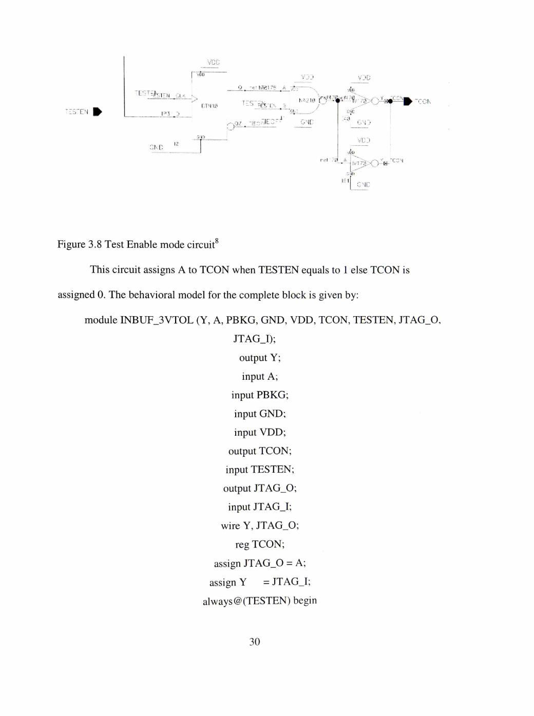
Figure 3.8 Test Enable mode circuit
This circuit assigns A to TCON when TESTEN equals to 1 else TCON is
assigned 0. The behavioral model for the complete block is given by:
module INBUF_3VTOL (Y, A, PBKG, GND, VDD, TCON, TESTEN, JTAG_0,
JTAG_I);
output Y;
input A;
input PBKG;
input GND;
input VDD;
output TCON;
input TESTEN;
output JTAG_0;
input JTAGJ;
wire Y, JTAG_0;
reg TCON;
assign JTAG_0 = A;
assign Y = JTAGJ;
always®(TESTEN) begin
30

if (TESTEN == 0) begin
TCON = 0;
end else begin
if (TESTEN == 1) TCON = A;
end
end
endmodule
Some of the modules have a delay operator. This is used to introduce time into the
simulation models of hardware components. In order to specify the time units for the
delay values, a 'timescale compiler directive is used. The form of compiler directive is
'timescale <time_unit>/<time_precision>. This directive sets the time units and precision
for the modules that follow it. The <timeunit> and <time_precision> entries are an
integer followed by a unit of time measure. Most of the modules have a 'timescale
directive of Ins/lps. This directive maintains time to the precision of 1 picosecond. The
values specified in delays though are multiples of 1 nanosecond. That is, #0.1 means
delay of 0.1 nanosecond. Thus models for many modules are created.
3.6 ASIC libraries
The serial transceiver design consists of numerous gates. Most of the gates are
basic gates, like not, and, or, nand etc. In addition to these there are different
multiplexers, Ex-or gates with different numbers of inputs. Some of the blocks are
synthesized blocks. These blocks are generated from a behavioral model with synthesis
tools. In the synthesis process, the tool gives a gated net list from a behavioral model A
31

library that consists of all gates is given to the tool and the synthesis tool generates the
net list using that library. That library has the behavioral models for all the gates. That
library is maintained as a separate file and is simulated along with the top-level model. So
whenever a particular gate is instantiated in a block, the respective model will be
accessed.
3.7 Net list from schematic
Once the models are created for different blocks the net list is generated. This net
list contains all these models and they are instantiated according to the presence of the
blocks in the complete design. A top-level verilog model of the serial transceiver is the
generated verilog net list of the complete design from the schematic. This net list
extraction can be done using Cadence (Design development and testing tool). Cadence
can dump out the verilog net list from the schematic. The generated net list is the
integration of the stmctural net list for some blocks, synthesized net list for some blocks
and behavioral models for some modules. While generating the net list the levels of
abstraction can be specified. There are different levels of abstraction from which Cadence
can dump out the net list. By mentioning the stop levels in a particular order, the net list
can be generated according to the desired level of extraction. In this particular design the
stop order is behavioral, functional, schematic, layout and symbol This is applied to the
complete design. This stop order is important in order to generate the behavioral models
instead of stmctured net list for the modules that have behavioral models.
32

The main module or the top-level module in the generated net list has all the ports
and their declarations. This module consists of all the instantiations and connections of
the sub blocks of the transceiver. The following is the main module and port declarations
of the serial transceiver.
module TOP_TLK3104SA (MF_A, MF_B, MF_C, MF_D, RBC_A, RBC_B, RBC_C, RBC_D, RXDAO. RXDAl, RXDA2, RXDA3. RXDA4, RXDA5, RXDA6, RXDA7, RXDA8, RXDA9, RXDBO, RXDBl, RXDB2, RXDB3, RXDB4, RXDB5, RXDB6, RXDB7, RXDB8. RXDB9, RXDCO, RXDCl, RXDC2, RXDC3. RXDC4, RXDC5, RXDC6, RXDC7, RXDC8, RXDC9, RXDDO, RXDDl, RXDD2, RXDD3, RXDD4, RXDD5, RXDD6, RXDD7, RXDD8, RXDD9, TDO, TXAN, TXAP, TXBN, TXBP, TXCN, TXCP, TXDN, TXDP, MDIO, CODE, CONFIGO. CONFIGl, DVADO, DVADl, DVAD2, DVAD3, DVAD4, ENABLE, GND, GNDA, LPENA, LPENB, LPENC, LPEND, MDC, PRBSEN, PSYNC, RFCN, RFCP, RSTN, RXAN, RXAP, RXBN, RXBP, RXCN, RXCP, RXDN, RXDP, SYNCEN, TCA, TCB, TCC, TCD, TCLK, TDI, TEST_EN, TMS, TRSTN, TXDAO, TXDAl, TXDA2, TXDA3, TXDA4, TXDA5, TXDA6, TXDA7, TXDA8, TXDA9, TXDBO, TXDBl, TXDB2, TXDB3, TXDB4, TXDB5, TXDB6, TXDB7, TXDB8, TXDB9, TXDCO, TXDCl, TXDC2, TXDC3, TXDC4, TXDC5, TXDC6, TXDC7, TXDCB, TXDC9, TXDDO, TXDDl, TXDD2, TXDD3, TXDD4, TXDD5, TXDD6, TXDD7, TXDD8, TXDD9, VDD, VDDA, VDDQ, VREF);
output MF_A, MF_B, MF_C, MF_D, RBC_A, RBC_B, RBC_C, RBC_D, RXDAO, RXDAl, RXDA2, RXDA3, RXDA4, RXDA5, RXDA6, RXDA7, RXDA8, RXDA9, RXDBO, RXDBl, RXDB2, RXDB3, RXDB4, RXDB5, RXDB6, RXDB7, RXDB8, RXDB9, RXDCO, RXDCl, RXDC2, RXDC3, RXDC4, RXDC5, RXDC6, RXDC7, RXDC8, RXDC9, RXDDO, RXDDl, RXDD2, RXDD3, RXDD4, RXDD5, RXDD6, RXDD7, RXDD8, RXDD9, TDO, TXAN, TXAP, TXBN, TXBP, TXCN, TXCP, TXDN, TXDP;
inout MDIO; input CODE, CONFIGO. CONFIGl, DVADO, DVADl, DVAD2, DVAD3, DVAD4,
ENABLE, GND, GNDA, LPENA, LPENB, LPENC, LPEND, MDC, PRBSEN, PSYNC, RFCN, RFCP, RSTN, RXAN, RXAP, RXBN, RXBP, RXCN, RXCP, RXDN, RXDP, SYNCEN, TCA, TCB, TCC, TCD, TCLK, TDI, TEST_EN, TMS, TRSTN, TXDAO, TXDAl, TXDA2, TXDA3, TXDA4, TXDA5, TXDA6, TXDA7, TXDA8, TXDA9, TXDBO, TXDBl, TXDB2, TXDB3, TXDB4, TXDB5, TXDB6, TXDB7, TXDB8, TXDB9, TXDCO, TXDCl, TXDC2, TXDC3, TXDC4, TXDC5, TXDC6, TXDC7, TXDC8, TXDC9, TXDDO, TXDDl, TXDD2, TXDD3, TXDD4, TXDD5, TXDD6, TXDD7, TXDD8, TXDD9, VDD, VDDA, VDDQ, VREF;
After the verilog net list is generated, test benches can be written in verilog to test the net
list. At-speed tests are explained in next two chapters.
33
CHAPTER W
TEST BENCHES
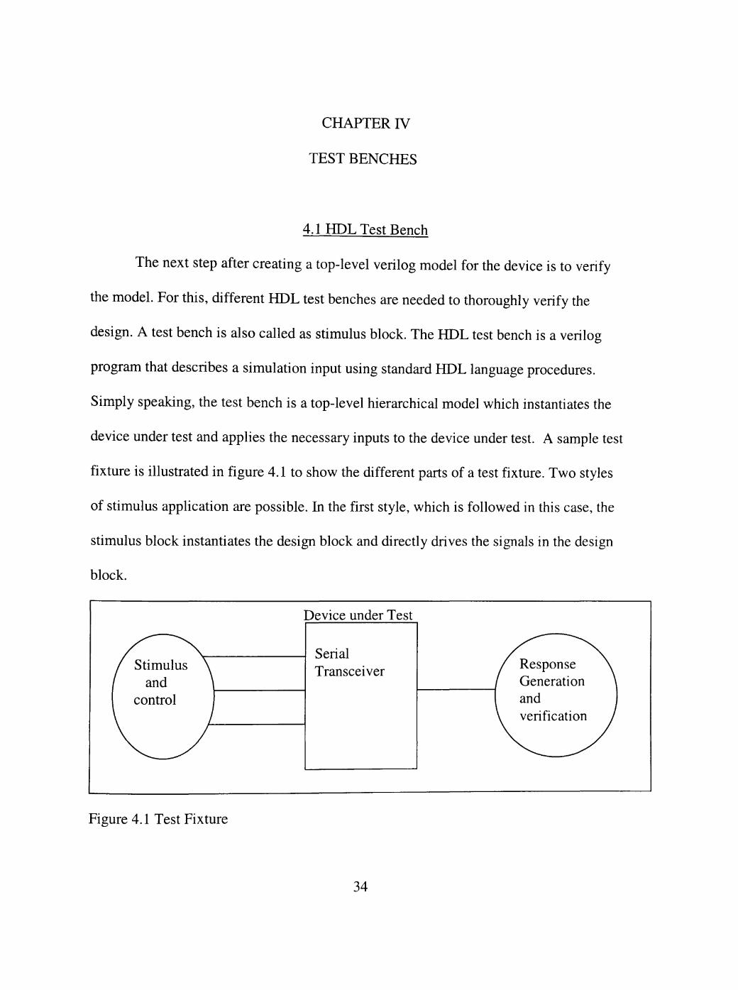
4.1 HDL Test Bench
The next step after creating a top-level verilog model for the device is to venfy
the model. For this, different JEDL test benches are needed to thoroughly verify the
design. A test bench is also called as stimulus block. The HDL test bench is a verilog
program that describes a simulation input using standard HDL language procedures.
Simply speaking, the test bench is a top-level hierarchical model which instantiates the
device under test and applies the necessary inputs to the device under test. A sample test
fixture is illustrated in figure 4.1 to show the different parts of a test fixture. Two styles
of stimulus application are possible. In the first style, which is followed in this case, the
stimulus block instantiates the design block and directly drives the signals in the design
block.
'. Device under Test
Serial Transceiver Response
Generation and verification
Figure 4.1 Test Fixture
34
The other style of applying stimulus is to instantiate both the stimulus and design
blocks in a top-level dummy module. The stimulus block interacts with the design block
only through the interface. In the test bench, data types of all the inputs and out puts need
to be declared. They can be declared as wire or reg. In verilog HDL, wire is the default
net type. But if a signal value changes in the stimuli, then it should be declared as reg. A
reg, or register, holds its value until a new value is assigned to it. More than one net or
wire can be declared in the same declaration by using a list of names separated by
commas. Similarly, more than one register can be declared by using the list of names
separated by commas. Also there are no ports for the test fixture. Below is a sample test
bench.
^timescale 1 ns / 1 ns
module testbench {);
// Data type declaration
// Apply stimulus
// Instantiate modules (Top level verilog module)
// Display results (In this case, create a dump file which can be viewed through a wave form viewer)
// endmodule
The stimulus part of the test fixture is specified inside a procedural block. There
are two types of procedural blocks. One is an initial procedural block, which executes
only once, and the other is an always procedural block, which executes in a loop. In
order to display results the verilog- $dumpvars command is used. A better method to
view signals as waveforms is available when Verilog is used m conjunction with a
35

waveform-viewing tool. The Verilog $dumpvars command is used to generate a value
change dump (vcd) file which stores the data for a large number of signals. Once the vcd
file has been created it can be displayed with the waveform-viewing tool. The file can
also be examined and displayed while the simulation is proceeding, if post processing is
not acceptable. In the waveform-viewing tool, a much larger selection of signals is
available. When using the $dumpvars command, only the waveforms of the desired
signals are used. These signals or pins are hsted in the bracket following the command.
This saves in reducing the vcd file size. If nothing is mentioned then all the available
signals are dumped out.
4.2 Transceiver instantiation
For this example, in each test bench, the serial transceiver is instantiated. The serial
transceiver instantiation is shown below. TOP_TLK3104SA is the module name given
for the top-level verilog model.
T0P_TLK310 4 SA UT0P_TLK310 4 SA(.TXDAO(txda[0] ) , .TXDAl(txda[1 ] ) , .TXDA2(txda[2]), .TXDA6(txda[6]) .TXDBO(txdb[0]) .TXDB4{txdb[4]) .TXDB8(txdb[8]) .TXDC2(txdc[2]) .TXDC6(txdc[6]) .TXDDO(txdd[0]) .TXDD4(txdd[4 J) ,TXDD8(txdd[8])
,TXDA3(txda[3]), .TXDA7(txda[7]) .TXDBl(txdb[1]) .TXDB5(txdb[5] ) .TXDB9(txdb[9]) .TXDC3(txdc[3]) .TXDC7(txdc[7]) .TXDDl(txdd[1]) .TXDD5(txdd[5]) .TXDD9(txdd[9])
,TXDA4(txda[4]), .TXDA8(txda[8]) .TXDB2(txdb[2]) .TXDB6(txdb[6]) .TXDCO(txdc[0]) .TXDC4(txdc[4]) .TXDC8(txdc[8]) .TXDD2(txdd[2]) .TXDD6(txdd[6])
.TXDA5(txda[5]), .TXDA9(txda[9]) .TXDB3(txdb[3]) .TXDB7(txdb[7]) .TXDCl(txdc[l]) .TXDC5(txdc[5]) .TXDC9(txdc[9]) .TXDD3(txdd[3]) .TXDD7(txdd[7])
,TCA(tea), .TCB(tcb), TCC(tec), .TCD(tcd), .RBC_A(rbc„a), .RBC_B(rbc_b), .RBC_C(rbc_c) , .RBC_D(rbc_d) , .MF_A(mf_a), .MF_B(mf_b) , .MF_C(mfc_c) , .MF_D(mf_d) , .MDIO(mdio) , .CODE(code), .CONFIGO(configO) , .CONFIGl(configl), .DVADO(dvadO) , .DVADl(dvadl) , .DVAD2(dvad2) , .DVAD3(dvad3), .DVAD4(dvad4) , .ENABLE(enable), .GND(gnd), .GNDA(gnda), .LPENA(Ipena), .LPENB(Ipenb) , .LPENC(lpenc), .LPEND(Ipend) , .MDC(mdc), .PRBSEN(prbsen) , .PSYNC(psync), .RFCN(rfcn), .RFCP(rfcp), .RSTN(rstn), .RXAN(txan),
36

RXAP(txap),RXBN(txbn),.RXBP(txbp),.RXCN(txcn),.RXCP(txcp),.RXDN(txdn) .RXDP(txdp),.TXAN(txan),.TXAP(txap),.TXBN(txbn),.TXBP(txbp), TXCN(txcn) , .TXCP(txcp) , .TXDN(txdn) , .TXDP(txdp), .SYNCEN(syncen) , .TCLK(tclk) .RXDAO(rxdaO), .RXDAl(rxdal). .RXDA2(rxda2) .RXDA4(rxda4), .RXDA8(rxda8), .RXDB2(rxdb2) .RXDB6(rxdb6), .RXDCO(rxdcO), .RXDC4(rxdc4), .RXDC8(rxdc8), .RXDD2(rxdd2) .RXDD6(rxdd6),
•RXDAl(rxdal) .RXDA5(rxda5) , .RXDA9(rxda9) , .RXDB3(rxdb3) .RXDB7(rxdb7), .RXDCl(rxdcl), .RXDC5(rxdc5), .RXDC9(rxdc9), .RXDD3(rxdd3)
.RXDD7(rxdd7), .TDI(tdi), .TEST_EN(test_en) .VDDA(vdda));
.RXDA6(rxda6), •RXDBO(rxdbO), .RXDB4(rxdb4)
.RXDB8(rxdb8),
.RXDC2(rxdc2),
.RXDC6(rxdc6),
.RXDDO(rxddO), .RXDD4(rxdd4) .RXDD8(rxdd8),
.RXDA3(rxda3) .RXDA7(rxda7) , .RXDBl(rxdbl), .RXDB5(rxdb5)
.RXDB9(rxdb9),
.RXDC3(rxdc3),
.RXDC7(rxdc7),
.RXDDl(rxddl), .RXDD5(rxdd5) .RXDD9(rxdd9),
.TMS(tms), .TRSTN(trstn), .VDD(vdd)
This instantiation is common in all the test benches.
4.3 Master file
As there are different test benches and different files, a master file is created to
simulate the required files. In the master file the asic library file, the top-level model file
and the test bench file is mentioned. A sample verilog master file is illustrated in Figure
4.2.
//acceleration options //-a +caxl +switchxl -i-no_turbo //get rid of annoying wamings -i-nowamTFNPC -i-libext-i-.v-i--y/db/asic_hbs/tsc5000_1.0/sun5/verilog/lib/2.5v (asic library file) // Model component files /sim/TLK3104SA.v (Top level verilog model) // Testbed file ASYNC TB.v
Figure 4.2. Master file
37

This verilog master file is simulated using Verilog-XL software. Verilog-XL is a
high-speed, event driven logic-level simulator that reads verilog HDL and simulates the
description to emulate the behavior of real hardware. Verilog-XL software can be started
from a command shell using the following command.
Verilog -f verilogjnaster.v
The master file is common for all the test benches except the test bench file. Only the test
bench file will be changed according to the required test.
4.4 Clock set-up
As mentioned before, all the at-speed verification will be done at al56 MHz
reference clock. In this device, there is a differential reference input clock, which is given
by pins RFCN and RFCP. The transmit data clock for each channel is provided through
pins TCA, TCB, TCC and TCD. The data on TDx[0..9] is latched on the rising and
falling edges of these clocks. The clock set up in all the test benches is similar except in
ASYNC test. The reference clock set up in the test bench is shown below.
// parameters
// fref is 160 MHz, hence ref2 which is half the period = 3.125 ns
parameter ref2 = 3.125;
// :H***************** Define the clocks rfcn, rfcp ******************
initial begin rfcp<=rb0;
r fcn<=rbl ; end
always #ref2
38

rfcp = -rfcp ; always @(rfcp)
rfcn <= -rfcp ;
Below is the clock-set up for the channel A transmit clock.
// ********* clock setup for channel A ************** // *******initiahze elk to 0 and then start mnning it after a delay******
initial begin
count = I'bO; tca=rbO;
#6.25 tca=l'bO; while(count < 1000) #ref2 tea = -tea;
count = count -I- 1; end
The clock set up for other channel clocks is the same as channel A
4.5 Top-level simulation plan
Figure 4.3 gives the list of top-level simulation plans that are performed to verify
the functionality. At-speed simulations are done at 160 MHz or a 156 MHz reference
clock.
39

At-speed Functionality
1. PRBS Extemal and Intemal modes
2. PRBSPOWER
3. SERDES with EN/DEC on and off
4. 10 Gig mode
5. ASYNC mode
Figure 4.3 Top-level simulation plan.
40

CJIAPTER V
AT-SPEED VERIFICATION
5.1 PRBS Testing
As mentioned in Chapter II, the serial transceiver has a built-in PRBS generator
and verifier. PRBS testing is necessary to check the functionality of the generator and
verifier blocks in the serial transceiver. This function can be enabled through an extemal
pin PRBSEN. When enabled, a PRBS pattem is generated and is supplied to the
serializer. This data is then fed back to the receiver. In the receiver, there is a PRBS
verification block, which checks the in coming pattem with the known PRBS pattem.
Data from the normal input source is ignored during the self-test mode. There are two test
modes, the PRBS extemal mode and the PRBS intemal mode. In the PRBS extemal
mode, the LOOPEN pin is set low. When the LOOPEN pin is set low, it disables the loop
back mode on the channel. When set high, it enables the loop back mode. This pin is
available on all four channels.
5.1.1 PRBS Extemal mode
To test the PRBS extemal function, the extemal pin PRBSEN is assigned 1 in the
test bench. The LPEN pin, which controls the loopback mode, is set to 0. Reset pin RSTN
is set to 0. The PRBSEN pin is set to 1 after the RSTN pin is set to 1. There should be at
least one clock cycle delay between them. This is done to reset the entire device. Figure
41

5.1 shows the simulation results of PRBS extemal testing for channel A. The result of the
test is verified through the pin A_PRBS_PASS_D. when this pin goes high, it indicates
that it received the correct PRBS pattem.
PRBSEXT -2
C,ro:>v •• A
c o d e •- 0
c o n f i g O .L. 0
c o n f i g l 0
e n a b l e -~ I
lp«'n.f> •- a
p r b s e n - I
r b c ^ a - (>
i f c p 1
.rfc.-n " (;
r s t n " 1
sy: :cen = 0
r:ca - z
tciH - a
test_«!•>. •= 0
t r j i ' .n - :,
•;xap ;
t x d a % ; g ; 0 | ' h EZZ
rx ! f e%(9 :0 ; •!] OGO
A..PK.BS. F-A..<>,3.„D 0
iCursr r !
( , I :
> ; 1
> : i j
1 :
u ^....
» 1 0 0 n s
. 1 '•' 0 '
..._.
r . j r s o r n .. 4717.<J76 rss;
•
! : :
1 1
> : 1 ;
t :
' : " - " - - M H I ^ ^ ^ H I I ^ ^ ^ H . •
C(>0 ' m^^^^mmm^^m ,i..
J 1 • .._
Pfinsid sn Sar! ?«[! J(>0:2>«! ?«:• *-T--i1',vi :>-, S iy ^ii'i^fji' !<, '^ri !-.;rT> ;. a?*t''.»- [V-i^i;- -Ji^-^e-n* ^
Figure 5.1. Simulations results for PRBS extemal testing
From the results, even though the PRBSEN pin goes high at 100ns,
A_PRBS_PASS_D pin goes high at around 3400ns. This delay is because of the time
taken for the entire device to reset and activate all the blocks.
42

5.1.2 PRBS Intemal mode
In this mode all the pins except the LPEN pin are same as in the PRBS extemal mode.
In this mode, the LPEN pin is set to 1. This enables the loop back mode. In the top-level
module instantiation, the high-speed input pins RXAP/RXAN are connected to the high
speed output pins TXAP/TXAN. This enables the high-speed serial data to be fed back to
the device. These pin instantiations are shown below:
.RXAN(txan),.RXAP(txap),.RXBN(txbn),.RXBP(txbp),.RXCN(txcn),.RXCP(txcp),
.RXDN(txdn), .RXDP(txdp),
.TXAN(txan),.TXAP(txap),.TXBN(txbn),.TXBP(txbp),.TXCN(txcn),.TXCP(txcp),
.TXDN(txdn),.TXDP(txdp),
Figure 5.2 shows the simulation results for PRBS intemal testing of all four channels.
From the results, the A_RSTN pin goes high around 3400ns. This is the intemal pin that
goes high when the entire device is reset.
43

PRBSINT -1 •J4irt'<»f*r> Ti;infl'ai8, aCTil/R/l
C u r s o r l - " , 2 5 0 , 6 5 4 . 6 6 9 p:
^TiiceA 0(0} p s 0 , 1 , 0 0 0 , 0 0 0 ,^,GOO,OOP ,S,?0"i COO 4 ,000 OOP .5.(>U0 OOP 5 9 * , 9 8 j r s
G r o u p : A
code 0
c c a f i g O = 0
c o n f i g l - 0
i p e n a 1
i p e n b - 1
I p e n c 1
I p e c d 1
p r b s e n - 1
t e s t „ e 4 i ^ 0
sy . i cen ^ 0
^PRB.S^..PASS_!J I
A_RS'ni' = 1
,_PRBS._PA.SS„D •= 1 _PRBS.._.PASS_D I 1
.^PRBS..PA.';$_D - 1
S
' "Tr*2 (X 3-j f &*p 2 01 CO 2^ 20!.. • •T-r.-po r*> v^'jiis.c*'^ ti ' ^1 '-OX C»-3e >:y 0*-^:.y'^r-stw-^ i
Figure 5.2. Simulation results for PRBS intemal testing.
5.2 PRBSPOWER Test mode
In the previous test modes, the device is tested for the intemal PRBS generator
and verifier blocks. But another test bench is required to test whether the device can
handle the extemal PRBS pattem. In this mode an extemal PRBS pattem is given to the
device through the parallel inputs TXDA, TXDB, TXDC, TXDC for all four channels.
This pattem is then checked on the parallel outputs RXDA, RXDB, RXDC, RXDD. The
inputs given to the device through the test bench are shown in Figure 5.3.
44

PRBSPOWER -4 t.«iayKj 4n T;,fT>mi(ia, aOi;'''S?i
3311 i « 9
Group: A
c o d e 1
c o n f i g O 0
c o n f i g l = 0
dvadO ^ I
e n a b l e - i
tr-c-C ii. 1
sndio »• 1
p r b s e n - 0
p s y n c - 0
r b c _ a i= -i
r f c n i
r s u i - I
syliceri 1
t e a • C
CCiic - 1.
t d i - 1
t e . ' s t . o a G
t n s - 1
t r s t n ... 0
txAa\9:Ql - 'h l a c
t x d b f 9 ; f ! ! - ' h iBC
t x d c ( S ; 0 | ' h l a c
t,stadE9.;0i - ' h XBC
C u r s o r l . • J313 a s Its
:i :s} i .'is 4 0
•Cursor:; - 3 3 5 1 . 1 3 n s
150 , 3 J 6 0 3 3 " "> , 6 8 5 r. s
J \ ^ ^l^
~~\ I
i ": ;
. .1 • I
I : r
r
!
n
(
1 1 1
r
1 "
!
, , ,|
1 r~
i
~ l _
t
1
r 1
u
: 1 1 • ! i L ._J L ;
: 1 i i !
l_
^ -
1 : 1
:
~n r"
000
000 oco
ll,BC
____Jia£ t lBC
Icso TrTTip
icio_ Icso
! i « ; l=5V
T'lCJ
|0r-> If)rs
llBC
I :BC
l;f«^
•0^0
:u50
i050
llBC
l l B C
hBr
Toes
Iocs „j™__-.
tOiO
jOi?
iGiO
!coc loo-looc looc
Iocs i013 IfrCD 1095
1QC5 1013 !0CI3 1095
iocs lOU iOCD 1095
Oir
JO:F
|02F
i o i c ioi"9 ;
j o i c joe? i l a i c !0C9 ;
1 ^^fFt(Ki [><i. Sal Sep 1 .^5y(>^*"'fs.'' P-''ttrta C.y S;ufwf5f J n « V ' "^^ Ca0a--'>"* 0***ny' :^)'V*<' * I't-
Figure 5.3 Input signals for PRBSPOWER test.
It can be seen that initial part of the parallel data consists of several comma or
K28.5 characters. The use of this K28.5 character is explained in Chapter II. More than
one K28.5 character is given so that byte synchronization can be done effectively. The
CODE pin is assigned I in order to enable 8B/10B encoding and decoding scheme.
Because the extemal PRBS pattem is fed to the device, the PRBSEN pin is set to 0 so
that there is no intemal PRBS generation. The SYNCEN pin is assigned 1. This pin,
when high, enables comma detection and byte alignment for all four-channels. The output
data signals are shown in Figure 5.4
45
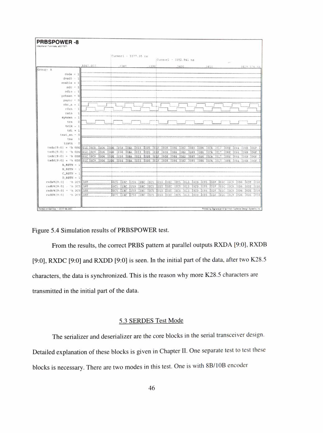
PRBSPOWER -8
1 3 7 - ' . 3 5 ::;;
:C 'J rsor2 - 3352 .941 n s
G r o u p ;
dvadO
e n a b l e
urfc
n d i o
p rbsep .
psy:ic
rbc,.ffl
r £ c n
r a t n
s y n c e n
tea
t c l k
t t J i
t>»3t_eri
tmi3
t x d a ! 9
txc ib lS
t x d d { 9
rxda% i
rx<4b%!9
r>:de%{9
rxd.-i*19
•b
» ' h
= ' h
.RSTN
.RSTK
' b
' h
- ' h
CDS
3 3 & 7 . 0 - V , l . . i 'JO:
r 1 ('" 1 .„ r 1 r
! r'"
n'cl'oc9~To5i~IoF£" io-sa IOSA !O?,3 IOCS JQiy 'oos ioas IQE.'> joea f056 [OCA :O I7 jcag io64 TO6B TO??
QIC iOC9 0136 jOSiE lOa^ 1033 lODS iOJF jOOS. | 0 e 6 |SS2 J089 j o s s lOCft 1017 iOBE loe^: ; 6 3 I06F T
2C5
2C5
2CS
MCLE5.9 TOPS TO^E Tij.')'B n)BA'T333 TODS'TQI'F TOO?, loss" ICE2~lo8<r"T6E6 TQCA ioiT~To8E la^A !o»3 lofeFT
QIC Iocs "TODS iote" loss IPSA I033 IOD5 loip IOOB j036 log; less joss IOCA :OI7 ^ORE Tos4~Tofea"Tot-F 1'
3FF toe5 lig»5"To?oTiic" IccT Ic^iF Iboc !"o<Jo~T"6i3 "loco [095 lo2.-"~'loic iocs |op6 |ODE l-ng 3FF t0C5 j l ' s c l o ' S O ' T r B C Iocs JOIC ISOC iac.5 iC13 lOCD l0?5 i02.=' iO lC jOc;? |OP6""]OCE T058
3FF 'T5"c5 T T i c T o l o i I B C Tecs |;)TD~IOOC JOC5""TOI3 IOCD'IOSS io2F loi"(f~]oc'J""IaD6"ToDE !o-)«
3FF iocs liBc Icso jiBc l o c f t?"i'o'"~16oc "Toes io"i3 locb T095 J02r- loic lov9ToanoaE"
I pT«it»c on Sai Stsp 5 ?;! ?? £« i W ^ nifw; Lf,' 3v' '*^.i^'^ ^ H-' '^^^ ^-aiv*^ 0«^»^" 3>'Vt»T
Figure 5.4 Simulation results of PRBSPOWER test.
From the results, the correct PRBS pattem at parallel outputs RXDA [9:0], RXDB
[9:0], RXDC [9:0] and RXDD [9:0] is seen. In the initial part of the data, after two K28.5
characters, the data is synchronized. This is the reason why more K28.5 characters are
transmitted in the initial part of the data.
5.3 SERDES Test Mode
The serializer and deserializer are the core blocks in the serial transceiver design.
Detailed explanation of these blocks is given in Chapter II. One separate test to test these
blocks is necessary. There are two modes in this test. One is with 8B/10B encoder
46

decoder on and other with 8B/10B encoder decoder off. This is controlled with the
CODE pin. All other inputs except transmit data (TXDA, TXDB, TXDC, TXDD) are the
same for both tests.
5.3.1 EN/DEC Off
This mode is set when the CODE pin is assigned to 0. This mode is called the
SERDES mode. In this mode, the transmit data bus for each channel accepts 10 bit wide
8B/10B encoded data at TXDx [0...9] pins. Data is latched on the rising and falling edge
of the transmit data clock. The data is then phase aligned to the reference clock
(RFCP/RFCN), serialized, then transmitted sequentially over the differential high speed
serial transmit pins TXxP/TXxn. Then the receive data bus for each channel outputs a 10
bit wide 8B/10B encoded data on RDx[0:9]. In this mode instead of normal 8-bit K
characters, encoded 10-bit K characters are given for comma detect and byte alignment.
The normal 8-bit and encoded 10-bit K-characters are given in Table 5.1
47
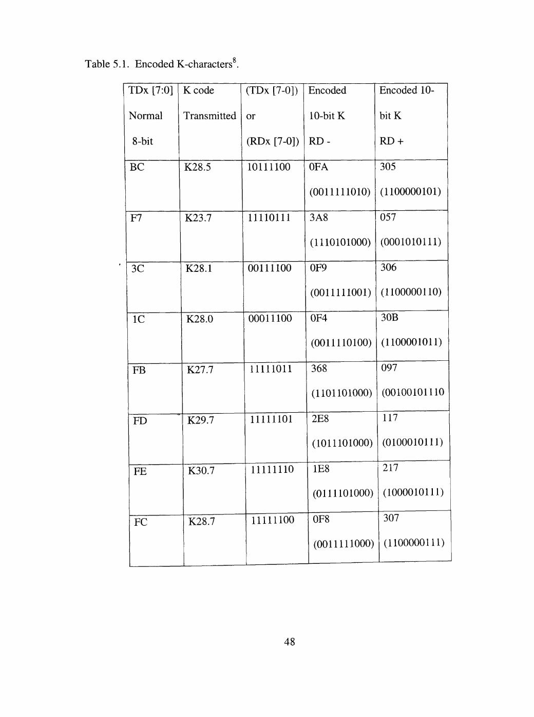
Table 5.1. Encoded K-characters^.
TDx [7:0]
Normal
8-bit
BC
F7
3C
IC
FB
FD
FE
FC
Kcode
Transmitted
K28.5
K23.7
K28.1
K28.0
K27.7
K29.7
K30.7
K28.7
(TDx [7-0])
or
(RDx [7-0])
10111100
11110111
00111100
00011100
union
11111101
11111110
11111100
Encoded
10-bit K
RD-
OFA
(0011111010)
3A8
(1110101000)
0F9
(0011111001)
0F4
(0011110100)
368
(1101101000)
2E8
(1011101000)
1E8
(0111101000)
0F8
(0011111000)
Encoded 10-
bitK
RD +
305
(1100000101)
057
(0001010111)
306
(1100000110)
30B
(1100001011)
097
(00100101110
117
(0100010111)
217
(1000010111)
307
(1100000111)
48

The parallel input data given to each channel A in the verilog test bench through
the TXDA pins is shown below. Similar data is given for the other channels.
//******* input 10 bit data stream to transmitter link ******
initial begin
#3385 #10.88 txda #ref2 txda = #ref2 txda = #ref2 txda = #ref2 txda = #ref2 txda = #ref2 txda = #ref2 txda = #ref2 txda = #ref2 txda = #ref2 txda = #ref2 txda = #ref2 txda = #ref2 txda = #ref2 txda =
= 10'b001 111 1010;//OFA lO'bOlOlOOOOll: lO'bOOl 1111010; lO'bl 100110100; lO'bOOl 1111010; lO'bl 100001011 lO'bOOl 1111010: lO'bllOlOllOll: lO'bOOlll 11010; lO'blOlOOlOllO; lO'bOlOlllllOO; lO'bllOlOlOlOO; lO'bOOOOOlllll; lO'bOl 10000010; lO'blOOOlOlOOO;
//OFA
//OFA
//OFA
//OFA
In the test bench, the initial part of the data consists of several OFA characters.
This is the encoded K28.5 (BC) character. As indicated before, more than one K-
character is given in order to identify the byte boundary. The simulation results for this
test are shown in Figure 5.5.
49

SERDES -2
Group: .'•
codia
c o n f i g O
canlig'x
cour . t
e n a b l e
I p e n a
Bide
p r b s e r .
r ^xr.„j't
r £ c p
r s t n
syncer ,
t e a
t c l k
r.tps
t r s t r .
t x d a i 9 ; 0 S - ' h
t x d b i 9 :01 i-i ' h
txdc\'):0> ' h
t x c ' . < 5 ' 9 : 0 1 iii ' h
'•:.xdn
t x d p
VrSd
vdca
r'xda*. • 0 : ;) ... ' h
r-i(f*ij o?i Swn SAO ^ 00^1 .i*J i>y--5
. 3 3 3 5 . !•-
... 0
... g
11
:••• 0
- k
» 0
-• I
0
- I
- i 1
= s - I
« 0
000
000
yos a 00
iii 1
62'-^
:ri;r:B<:irI .. 33go.7}OOS rss : :':::'.!• sot2 3 536 -.'BOOS .is
• : M ' ' 9 ,-40C 3''Dr 3-4 4r.^-^ ^ ,
: ; n n n n n n n n m n n n n n n n n n n n n n n n n n r
.n..n. "u IJ"
LMF J LjTi'U"UTrixu"ijTnj"LnjiJi.RJi.ri_rLR_.RJT.n.ji.Jiii.ji_ri.n LJ L.fi.ri ri..njTJiii„rLn....rijTJi..rRn.n_ji_ruTnxLru'TjijTnj"u
i n j " [ j l j LJ- •u"""LJUlJ''uiTijTn.jTjTJi....riJin.„rji.rin.riJiJiJi.._rinxLn_riJ
oao 000
eoe 00 G
: , M M M hi M M M I'M M • 1 i-i M i M 1 M-l ! M i M i-J i i ; i M - : l i - i 1 M !>n M ; i n - i M i • i ' i-M ! ! 1 ! i M-M i t i M i- •
UM 1 M I'M M i M f; M ! . 1 : !<i n 1 1 ! i ! i-i 1 1 M i M-i ! 1 i : 1 ! . : M M M I'i n 1 M 1 hi M 1 M : i-! ! M 1 i M -1 1 i 1 n • l«! 11 ' 1 1
90].'' : : 1' 1 n M 11 i 11 M 1 I I M t 1 I i 1 M 1 1 • 1 M PrsitaKJ c>v S'S^ulE'rar ti ^s i *fi,/r. CisSS'X* ' i^wg" Syet*-. -. • i
Figure 5.5. SERDES with EN/DEC off test results.
5.3.2 SERDES with EN/DEC on
When the CODE pin is set to 1, the 8B/10B encoder decoder is on for each channel.
This mode is called the transceiver mode. In this mode, the transmit data bus for each
channel accepts 8-bit wide parallel data at the TDx[0...7] pins. The data is first aligned to
the reference clock, then 8b/10b are encoded and passed to the serializer. The TDx8
(KGEN) pin controls the generation of K-characters. When this pin is asserted, the
appropriate 8b/10b character is transmitted. The receiver data bus for each channel
50

outputs an 8-bit wide parallel data on RDx[0.. .7]. If an error is uncovered in decoding the
data, all I's (FF) are placed on the receive data bus for that channel. Figure 5.6 shows the
test results for this mode. The 3FF byte in the initial part of the receive data bus is
because of a data error before byte synchronization.
SERDES-ENDEC -3
C t i r a o r i = 2732 .4124X8 n s
. 2 7 3 2 . 4 1 2 4 1 8 ,2900 .3000 ,3500 G r o u p : A
coder
c o n f i g O - a
c s x i f i g l - 0
Ipersa .~ 0
e n a b l e i
p r b s e n - 0
p s y n c iii 0
s y n e e n iii 1
t r s r r i -. 0
txi-ia i 9 . 0 ; ' h 000
r x d a * ; 0 i 3 ! • Mi ODO
txab(?i»:OS - ' h QOO
r x d b l I S : 0 ! - ' h OQO
t x d c S 9 : 0 i - ' h 000
rxdc%i9- . Oi •- ' h 000
t . x a d ; 9 . 0 j ' h OCO
r.-^dc* ; 3 : Oi • ' h 'JOO
_. CurEor2 - 4 00 0
. i j oo ,"!;0o '-i':-} :•:'•: !<iu. 3^0" (.!i:.i 4^. •
."..S
0 G i"i
000
osc opo 000
900 ;) {•,;.
aiitiiiniiiiinipminffliiHifiKfiiinHimiiiu-11 >. r- (tiiiiiiBiiiniiiiiiiiiiiiiiiitiiiiuiiiiiiuiiu,..,
{iti)fiiiiiutiniiUii!ii{i»iiiiiHiU!fii>i^nBBBBB8 iijFF iiiiiiiiMinHiiiminninniHnHifnnniiffoif -
ill{|l!raillll!!illt!ll!llilitl!ailB!lllllllHlllli03f T S F F - 1
" • -
—
i liiiHi laiiinitiiiuiiii iiiimtiiJiiiiiimi i m H H H ^ i i ^i(llillilHlllI!iini!i!init!Hllll!IHilllllllHIIIII;3F
11 3 F F llitll{!llUlilllllitiiitilliliri!lll[lilltlllllli 0 3 r
1 s^i-i-r^^jj •::- s ,» . . S e : ' > (X' ^*) •!<; ?(>:^ P ::;?.-*••! >>, Si^--.;>iVtf *> = f l f^-.f-l •J-i->J-',X LVJS Qfi S • J!!?'"^- -<
Figure 5.6 Results of SERDES test with EN/DEC on.
5.4 10 GIG Mode
The serial transceiver consists of four channels. One of the important features of
this device is that it can function as four independent channels or as one 10 Gigabit
transceiver. This function is controlled by the PSYNC pin. When this pin is set to 1. the
51

device acts as a single 10 Gigabit Ethernet transceiver. In this mode, the device performs
serialization/deserialization and channel synchronization. Channels synchronization is
done using the channel A transmit (TCA) and receive (RCA) clocks. TCA/RCA are used
to clock in/out all channels of data. The data on all channel is synchronized and the
output is referenced to the extracted receive clock for channel A, RCA. In this mode the
PSYNC, CODE and SYNCEN pins are set high. The inputs given are shown in Figure
5.7.
10GIGMODE-2
J t
c o d e 1
c o s t igO i 0
c o n ; i q \ 0
ei^ah.^ e -• \
Ipeaa . o
Ipersb • 0
I p e n d - 0
l p e Q < i -••• 0
y r b s e n "• 0
p s y n c - I
r t c n ii 0
r f c p - 1
r s s 11 iii 1
t e d 1
s y n c e n ii 1
tS.»! •' \
t r s t - n iii 0
.••<«iKn4c<i*alS*)> ' 23;H; . I«2C«!
. 3 34 ^. -.11': • > ; >
^Cur .or3 3 3 6 0 , 5 0 5 n s :Ci i r sc r2 - 3573.005 r.s ^
! ! •
i. >. ,.,
« t
» 1
0 1 ^ if. .o .•>4r
"~ ' r 4~ — _i
c 1 ,. 1 T
1 8" 1,, <, 1 1 ^ ; iC'>C
1 <- 1 ,,n>, i o ; - , o , , , .••--i . ic , J M ' • l,':i'" I s , |oc;> xrc
, : B C IOCS !IBC :S5O ; i sc loo: ;002 [ooT^
: " 3 h,BC 1030 jiBC iooi !002 !oo4 iooa
|C3C I:BC iOCl !002 1004 i008 loio
ioso i i sc looi !0C2 ioo4 !oo8 :oio lo;c
1 " " L . _
' "1 1 1 1
1 1
J 1
t
[ \_. i [
' ,J ' i :
1 I ; i i • " " • • 1 ; ": '" I
..... , ..,._ ; \ i • i ...„„..j
. - ™-.,™™-™„™:^,-™»Wi™i-™w,
, . ; ^ ^
1 J ' 1 1
i ; 1 1 1... . r^~~\ r
L i ; I J "1 ' " 1 r
? ! i 1 1 i 1 \ i 1 i 1 ( i i
i 1 ! , i 1 ! i ^
1 r "••'•"""1 1^ i_. ...J L.. I - j | " " - i 1 - ] . 1 r
! i i 1 1 ; 1 ;
™ ,
Pi^?ii*.d L-> '}i^-'^ s.i^. ' . -.(i! ^< ii- . : j . t . ^ T i * Li.^..yi ' . . , ^ i . - . ' -i \
Figure 5.7 Inputs for lOGig test mode.
In Figure 5.7, between cursor 1 and cursor 2, data byte 17C is shown on each
channel. This is the K28.3 or A character. After this character, there is a K character on
52

each channel. The A character is responsible for channel synchronization. To test this
mode, in the test bench, the data is given so that there is a one byte delay between
channel A and channel B, channel B and channel C, channel C and channel D. The
device should synchronize all the four channels as soon as it sees the A character.
Figure 5.8 shows the results of this test.
10GIGMODE-4 i i^. jy ' .A j>- ' •.-.^: Mii.^ .Ki i • •.. T^
1 4 ^ <i i i 6 j 0 -• •.; '- > -J
C;:ciip: A
iL.\d,a i s :0) - ' h 020
f:xrlb!9.-01 i= ' h 020
Cx t3c i9 :0 ! ' h 020
C x d d f 9 : 0 ! .- ' h 3 7C.
Ci^ce ..- 1
c o n i i g O - 0
con f ig.I - 0
ertab.le .1
pr"bsen - 0
peyriC 1
rfc-i. 0
r f c p - 1
r s t n iii 1
syacen 1 t.l^S - I
t r s t r , i= 0
r x d a * rg. 'O! - ' h 000
rxdb«i ;9 . -a! - ' h 000
r:<dc%S9;01 'h 000
r«3c i%!? :0 ! - ' h 000
•^iO-' 35:35.221922 r,4!
i020 !o.»o iooi i:::: ;;,.i4 ••^.-:.<; ^ - i ?
. J M P J a 01 ,1003 [00 4, iOoa CIO i32 0 i
[ooi |002 |0C4 lOOB 1030 ;020 |040 I
li.!02 Joo4 .,Xoqs l a :o i020 ii'40 iooi ;
j . ; 0 i u 4 0
740 h'lO; 1
)oi ;oo; 1 502 i 0 0 4 i
0 0 1 :
0 0 2 i
0 0 4 i
OOS i
002 1004 ioos l o io !02u io-30 iooi iooa
004 IOO8 JOIO I02O 1040 iooi '002 iOO-S
008 I o i o lOiO 1040 iOC: 1002 i004 iO09
OiO 1G20 |040 lllOi lOviO !004 UiuB lOIJ
i i ' 1 ! i ;
i 1 j j ! i i j== l r n r i r ' \ ""i 1 1 ~ 1 1 ! ' 1 r
o*iO<;o iooi loo; iooa loos ioio io20 1040 il7C IB . - l i r r - Q5u liBC i o c s _ i l8C_ 1050 l l g O i O V
O'iOOl i002 iOO-S !00» (010 i020 1040 117C U B C i C ^ C U B C I O 5 0 [ : B C ioc5 l i s c !cbo ! : s c iO'
0"!O03 1004 1008 lOlO iOSb '340 I H C Uac ioso her lOFF lOSO IlBC iocs liBO: lC50 llBC lO-
0M004 1008 lOiO i020 iQ40 U?C IjBC iOSO i l B C 10'-s 1.5rr | 050 llSC |0C5 IlBC |050 IlBC jO'
Pt>f*8i]«>i) Sa> t>cc ( * J ? ^ 0 ' .iOO' '1 •' ^'J t>y -3 ;,• -ii Sv-ar 5 '^ 1 •'•>^--r '^a»^i^ '.i^^-'i- -i^^.-f'' •'
Figure 5.8 10 Gig mode outputs.
Figure 5.8 shows that all the channels are synchronized at 3515ns.
53

5.5 ASYNC Test mode
The final at-speed simulation consisted of two devices with their serial pins
interconnected. This test mode is developed to test whether the device can interact
effectively with the same device in different modes. In this test one device will act as a
transmitter and other as a receiver. Both the devices will run at different frequencies. The
device acting as a transmitter will have reference frequency of 156.032 MHz and the
device acting as receiver as 156 MHz. In the test bench the device will be instantiated
two times. One instantiation will have pins with tx prefix and other with rx prefix. The
test bench instantiation is shown in Figure 5.9.
11 ;i;*Hs:}:5i<;f;5f;>ic5}!********** Module Instautlatlons ******************************* // TX inst TOP_TLK3104SA TX_UTOP_TLK3104SA(.TXDA0(tx_txda[0]), TXDAl(tx_txda[l]), .TXDA2(tx_txda[2]), .TXDA3(tx_txda[3]), .TXDA4(tx_txda[4]), .TXDA5(tx_txda[5]), .TXDA6(tx_txda[6]), .TXDA7(tx_txda[7]), .TXDA8(tx_txda[8]), .TXDA9(tx_txda[9]), .TXDB0(tx_txdb[0]), .TXDBl(tx_txdb[l]), .TXDB2(tx_txdb[2]), .TXDB3(tx_txdb[3]), .TXDB4(tx_txdb[4]), .TXDB5(tx_txdb[5]), .TXDB6(tx_txdb[6]), .TXDB7(tx_txdb[7]), .TXDB8(tx_txdb[8]), .TXDB9(tx_txdb[9]), .TXDCO(tx_txdc[0]), .TXDCl(tx_txdc[l]), .TXDC2(tx_txdc[2]), .TXDC3(tx_txdc[3]), .TXDC4(tx_txdc[4]), .TXDC5(tx_txdc[5]), .TXDC6(tx_txdc[6]), .TXDC7(tx_txdc[7]), .TXDC8(tx_txdc[8]), .TXDC9(tx_txdc[9]), .TXDDO(tx_txdd[0]), .TXDDl(tx_txdd[l]), .TXDD2(tx_txdd[2]), .TXDD3(tx_txdd[3]), .TXDD4(tx_txdd[4]), .TXDD5(tx_txdd[5]), .TXDD6(tx_txdd[6]), .TXDD7(tx_txdd[71), .TXDD8(tx_txdd[8]), .TXDD9(tx_txdd[9]), .TCA(tx_tca), .TCB(tx_tcb), .TCC(tx_tcc), .TCD(tx_tcd), .RBC_A(tx_rbc_a), .RBC_B(tx_rbc_b), .RBC_C(tx_rbc_c), .RBC_D(tx_rbc_d), .MF_A(tx_mf_a), .MF_B(tx_mf_b), .MF_C(tx_mfc_c), •MF_D(tx_mf_d), .MDIO(tx_mdio), .CODE(tx_code), .CONFIGO(tx_configO), .CONFIGl(tx_configl), .DVADO(tx_dvadO), .DVADl(tx_dvadl), .DVAD2(tx_dvad2), .DVAD3(tx_dvad3), .DVAD4(tx_dvad4), .ENABLE(tx_enable), .GND(tx_gnd), .GNDA(tx_gnda), .LPENA(tx_lpena), .LPENB(tx_lpenb), .LPENC(tx_lpenc), .LPEND(tx_lpend), .MDC(tx_mdc), .PRBSEN(tx_prbsen), .PSYNC(tx_psync), .RFCN(tx_rfcn), .RFCP(tx_rfcp), .RSTN(tx_rstn), .RXAN(tx_rxan), .RXAP(tx_rxap), .RXBN(tx_rxbn),.RXBP(tx_rxbp),.RXCN(tx_rxcn),.RXCP(tx_rxcp),.RXDN(tx_rxdn),
.RXDP(tx_rxdp),.TXAN(tx_txan),.TXAP(tx_txap),.TXBN(tx_txbn),.TXBP(tx_txbp),.TX
CN(tx_txcn),.TXCP(tx_txcp),
Figure 5.9 Transceiver instantiation
54

.TXDN(tx_txdn),.TXDP(tx_txdp),.SYNCEN(tx_syncen),.TCLK(tx_tclk), .RXDAO(tx_rxdaO), .RXDAl(tx_rxdal), .RXDA2(tx_rxda2), .RXDA3(tx_rxda3), .RXDA4(tx_rxda4), .RXDA5(tx_rxda5), .RXDA6(tx_rxda6), .RXDA7(tx_rxda7), .RXDA8(tx_rxda8), .RXDA9(tx_rxda9), .RXDBO(tx_rxdbO), .RXDBl(tx_rxdbl), .RXDB2(tx_rxdb2), .RXDB3(tx_rxdb3), .RXDB4(tx_rxdb4), .RXDB5(tx_rxdb5), .RXDB6(tx_rxdb6), .RXDB7(tx_rxdb7), .RXDB8(tx_rxdb8), .RXDB9(tx_rxdb9), .RXDCO(tx_rxdcO), .RXDCl(tx_rxdcl), .RXDC2(tx_rxdc2), .RXDC3(tx_rxdc3), .RXDC4(tx_rxdc4), .RXDC5(tx_rxdc5), .RXDC6(tx_rxdc6), .RXDC7(tx_rxdc7), .RXDC8(tx_rxdc8), .RXDC9(tx_rxdc9), .RXDDO(tx_rxddO), .RXDDl(tx_rxddl), .RXDD2(tx_rxdd2), .RXDD3(tx_rxdd3), .RXDD4(tx_rxdd4), .RXDD5(tx_rxdd5),
.RXDD6(tx_rxdd6), .RXDD7(tx_rxdd7), .RXDD8(tx_rxdd8), .RXDD9(tx_rxdd9), .TDI(tx_tdi), .TEST_EN(tx_test_en),.TMS(tx_tms), .TRSTN(tx_trstn), .VDD(tx_vdd), .VDDA(tx_vdda)); TOP_TLK3104SA RX_UTOP_TLK3104SA(.TXDA0(rx_txda[0]),.TXDAl(rx_txda[l]), .TXDA2(rx_txda[2]), .TXDA3(rx_txda[3]), .TXDA4(rx_txda[4]), .TXDA5(rx_txda[5]), .TXDA6(rx_txda[6]), .TXDA7(rx_txda[7]), .TXDA8(rx_txda[8]), .TXDA9(rx_txda[9]), .TXDBO(rx_txdb[0]), .TXDBl(rx_txdb[l]), .TXDB2(rx_txdb[2]), .TXDB3(rx_txdb[3]), .TXDB4(rx_txdb[4]), .TXDB5(rx_txdb[5]), .TXDB6(rx_txdb[6]), .TXDB7(rx_txdb[7]), .TXDB8(rx_txdb[8]), .TXDB9(rx_txdb[9]), .TXDCO(rx_txdc[0]), .TXDCl(rx_txdc[l]), .TXDC2(rx_txdc[2]), .TXDC3(rx_txdc[3]), .TXDC4(rx_txdc[4]), .TXDC5(rx_txdc[5]), .TXDC6(rx_txdc[6]), .TXDC7(rx_txdc[7]), .TXDC8(rx_txdc[8]), .TXDC9(rx_txdc[9]), .TXDDO(rx_txdd[0]), .TXDDl(rx_txdd[l]), .TXDD2(rx_txdd[2]), .TXDD3(rx_txdd[3]), .TXDD4(rx_txdd[4]), .TXDD5(rx_txdd[5]), .TXDD6(rx_txdd[6]), .TXDD7(rx_txdd[7]), .TXDD8(rx_txdd[8]), .TXDD9(rx_txdd[9]), .TCA(rx_tca), .TCB(rx_tcb), .TCC(rx_tcc), .TCD(rx_tcd), .RBC_A(rx_rbc_a), .RBC_B(rx_rbc_b), .RBC_C(rx_rbc_c), .RBC_D(rx_rbc_d), .MF_A(rx_mf_a), .MF_B(rx_mf_b), .MF_C(rx_mfc_c), .MF_D(rx_mf_d), .MDIO(rx_mdio), .CODE(rx_code),.CONFIGO(rx_configO), .CONFIGl(rx_configl), .DVADO(rx_dvadO), .DVADl(rx_dvadl), .DVAD2(rx_dvad2), .DVAD3(rx_dvad3), .DVAD4(rx_dvad4), .ENABLE(rx_enable), .GND(rx_gnd), .GNDA(rx_gnda), .LPENA(rx_lpena), .LPENB(rxjpenb), .LPENC(rx_lpenc), .LPEND(rx_lpend), .MDC(rx_mdc), .PRBSEN(rx_prbsen), .PSYNC(rx_psync), .RFCN(rx_rfcn), .RFCP(rx_rfcp), .RSTN(rx_rstn), .RXAN(tx_txan), .RXAP(tx_txap), .RXBN(tx_txbn),.RXBP(tx_txbp),.RXCN(tx_txcn),.RXCP(tx_txcp),.RXDN(tx_txdn), .RXDP(tx_txdp),.TXAN(rx_txan),.TXAP(rx_txap),.TXBN(rx_txbn),.TXBP(rx_txbp),.T XCN(rx_txcn),.TXCP(rx_txcp),.TXDN(rx_txdn),.TXDP(rx_txdp),.SYNCEN(rx_syncen) ,.TCLK(rx_tclk), .RXDAO(rx_rxdaO), .RXDAl(rx_rxdal), .RXDA2(rx_rxda2), .RXDA3(rx_rxda3), .RXDA4(rx_rxda4), .RXDA5(rx_rxda5), .RXDA6(rx_rxda6), .RXDA7(rx_rxda7), .RXDA8(rx_rxda8), .RXDA9(rx_rxda9), .RXDBO(rx_rxdbO),
.RXDBl(rx_rxdbl), .RXDB2(rx_rxdb2), .RXDB3(rx_rxdb3), .RXDB4(rx_rxdb4),
.RXDB5(rx_rxdb5), .RXDB6(rx_rxdb6), .RXDB7(rx_rxdb7), .RXDB8(rx_rxdb8),
.RXDB9(rx_rxdb9), .RXDCO(rx_rxdcO), .RXDCl(rx_rxdcl), .RXDC2(rx_rxdc2),
Figure 5.9 continued
55

.RXDC3(rx_rxdc3), .RXDC4(rx_rxdc4), .RXDC5(rx_rxdc5), .RXDC6(rx_rxdc6), .RXDC7(rx_rxdc7), .RXDC8(rx_rxdc8), .RXDC9(rx_rxdc9), .RXDDO(rx_rxddO), .RXDDl(rx_rxddl), .RXDD2(rx_rxdd2), .RXDD3(rx_rxdd3), .RXDD4(rx_rxdd4), .RXDD5(rx_rxdd5), .RXDD6(rx_rxdd6), .RXDD7(rx_rxdd7), .RXDD8(rx_rxdd8), .RXDD9(rx_rxdd9), .TDI(rx_tdi), .TEST_EN(rx_test_en),.TMS(rx_tms), .TRSTN(rx_trstn), .VDD(rx_vdd), .VDDA(rx_vdda));
Figure 5.9 continued
After instantiating the device two times, the functionality of each will be
determined by the configuration pins CONFIGO and CONFIGl. In the test bench TX
configuration, pins tx_configO are assigned 0 and tx_configl are assigned 1. Thus, TX
instantiation is in the transmit only mode. RX configuration pins, rx_configO and
rx_configl are assigned to 1 and 0, respectively. Thus, RX instantiation is in receive only
mode.
In this test mode, the serial pins of the two devices are interconnected. The serial
transmit pins of the TX device(tx_txan/tx_txap, tx_txbn/tx_txbp, tx_txcn/tx_txcp,
tx_txdn/tx_txdp) are connected to serial receive pins of the RX device. The test consists
of sending Parallel data from the transmit bus of the TX device and is checked at the
receive data bus of RX device. Figure 5.10 shows the simulation results for this test.
56

ASYNC -3
' 4 8 . p 3
Oursa rO
,3, . > 1 2 , ' ; 4 8 .
lx_Cxdbi9
rx_txdc i 9
rx_r:<da*! 9
rx ry.at/t '9
rx,..rxdc%!9
ri<...r>:dd»!9
-h 000
-h 000
•h 0 00
•h 000
'h 000
•h 000
h ceo
•h 000
QOO
OOP
2M,..
Mil 000
,o.fi..c... .000
000
J21LMS- 40.OOP
l i 2 £ a . l l l a , iSCO l^Og 10A3 i>22 iJih fO'D 1038 '24R j / e
1.000
3 . J 6 « ,
3 5 " , ? 9 9 .
300 p s
? ? 9 T;S
12Cfe ! 0 9 ; i.lBC.~To1J~Tric."
0 2 F JQiC
i J B C J0C5
"TTic ro?(;""""TIic !"oc» UBC" -o^o UBC jOC5~T6ib" i--''^-
oc^ io:3 loita .ILBQ, Rl^e,, jXBO jOCS ilBC l a [IBC iSC5 [QIC iOCC j o e ; l-:-:; ln?5"
|2£^ | 15^ I iCO no :
. 1.= :
i G C 5 1 3 C J50
i"^»ij .:'5 Si,-. i> K, ^ -X' ! 5 ^3 .;>/,! * ";if.?J T. "'^'i.^iican *: 5«.1 ^f.^-'Ci'lftnc* ,>«»jn '^^•J-'ff-:^
Figure 5.10. ASYNC test results.
From the result, it can be seen that the receive data is exactly as the transmit data.
From this it can be concluded that the device is working properly.
57

CHAPTER VI
CONCLUSION
A top-level verilog HDL model for a large and complex design such as a
serial transceiver has been developed and verified functionally using different test
benches. Simulation results confirm the anticipated results. In any large-scale design, half
of the resources are invested in verifying that they function according to specification.
Design errors that escape verification may be discovered by customers, which may result
in dire consequences for the developer. The fundamental issue is meeting project
deadlines. Because of this there is a great need to speed up the verificadon process and
reduce simulation time.
With this approach of functional verification, the device has been verified at top-
level. In this process verification time has been reduced significantly with the help of
behavioral modeling. The simulation output files from these tests can be used to generate
test vectors. These test vectors can be used to test actual physical device. The added
advantage with this approach is re-usability. A lot of the behavioral models can be used
in other similar designs thus reducing developing and verification dme for other similar
designs.
This approach can be improved in terms of functional coverage. In this approach a
set of directed tests that cover known and supposed comer cases are generated. These
tests cover most of the funcdonality and verify most of the critical blocks in the design.
Generating a set of random tests to cover the remainder of functional space can increase
58

functional coverage. However with exploding design sizes, this manual approach of
creating tests of different functionalities becomes intractable. Engineers need a way to
create test generators that automatically generate large amount of high quality stimulus to
designs. This in tum can lead to increased functional coverage and faster verification
times.
59

REFERENCES
[1] Moorby, Philip R. and Thomas, Donald E., The Verilog Hardware Descriptive Language, 1998, Kluwer Academic Publishers, New York.
[2] Navabi, Zainalabedin Verilog HDL: Analysis and Design of Digital Systems, 1999, Mc Graw Hill, New York.
[3] Smith, Michael John Application-specific Integrated Circuits, 1997, Addison Wesley Longman, Glenview, IL.
[4] Seifert, Rich Gigabit Ethernet: Technology and Applications for High-speed LAN's, 1998, Addison Wesley Longman, Glenview, IL.
[5] Kang, Sung-Mo and Leblibici, Yusuf CMOS Digital Integrated Circuit Analysis and Design, 1998, Mc Graw Hill, New York.
[6] Palnitkar, Samir Verilog HDL: A Guide to Digital Design and Synthesis, 1996, Prentice Hall, Englewood Chffs, N.J.
[7] IEEE Draft P802.3ae/D2.1, 2001, IEEE Standards Department, New York.
[8] Serial Gigabit Solutions, TLK Cell Overview, 2000, Texas Instmments, Dallas, TX.
60

PERMISSION TO COPY
In presentmg this thesis m partial fulfillment of the requirements for a master's
degree at Texas Tech University or Texas Tech University Health Sciences Center, I
agree that the Library and my major department shall make it freely avadable for
research purposes. Permission to copy this thesis for scholarly purposes may be
granted by the Director of the Library or my major professor. It is understood that
any copymg or publication of this thesis for financial gam shall not be allowed
without my ftirther written permission and that any user may be liable for copyright
infringement.
Agree (Permission is granted.)
Student Signature Date
Disagree (Permission is not granted.)
Student Signature Date

PERMISSION TO COPY
In presenting this thesis in partial fiilfillment of the requirements for a master's
degree at Texas Tech University or Texas Tech University Health Sciences Center, I
agree that the Library and my major department shall make it freely avadable for
research purposes. Permission to copy this thesis for scholarly purposes may be
granted by the Du-ector of the Library or my major professor. It is understood that
any copymg or publication of this thesis for financial gam shall not be allowed
without my fiirther written permission and that any user may be liable for copyright
infringement.
Agree (Permission is granted.)
Student Signature Date
Disagree (Permission is not granted.)
Student Signature Date