Embed Size (px)
Citation preview
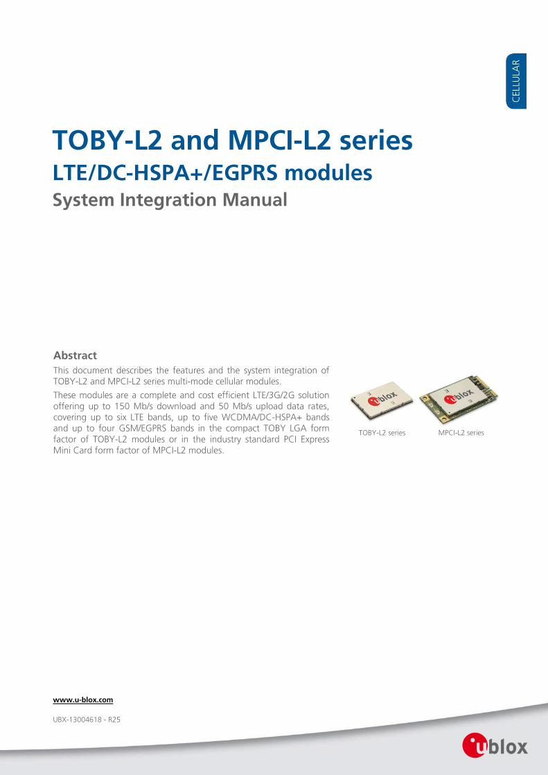
TOBY-L2 and MPCI-L2 series LTE/DC-HSPA+/EGPRS modules System Integration Manual
Abstract
This document describes the features and the system integration of TOBY-L2 and MPCI-L2 series multi-mode cellular modules.
These modules are a complete and cost efficient LTE/3G/2G solution offering up to 150 Mb/s download and 50 Mb/s upload data rates, covering up to six LTE bands, up to five WCDMA/DC-HSPA+ bands and up to four GSM/EGPRS bands in the compact TOBY LGA form factor of TOBY-L2 modules or in the industry standard PCI Express Mini Card form factor of MPCI-L2 modules.
TOBY-L2 series
www.u-blox.com
UBX-13004618 - R25
MPCI-L2 series
TOBY-L2 and MPCI-L2 series - System Integration Manual
UBX-13004618 - R25
Page 2 of 162
Document Information
Title TOBY-L2 and MPCI-L2 series
Subtitle LTE/DC-HSPA+/EGPRS modules
Document type System Integration Manual
Document number UBX-13004618
Revision and date R25 03-Jan-2018
Disclosure restriction
Product Status Corresponding content status
Functional Sample Draft For functional testing. Revised and supplementary data will be published later.
In Development /
Prototype Objective Specification Target values. Revised and supplementary data will be published later.
Engineering Sample Advance Information Data based on early testing. Revised and supplementary data will be published later.
Initial Production Early Prod. Information Data from product verification. Revised and supplementary data may be published later.
Mass Production /
End of Life Production Information Final product specification.
TOBY-L2 and MPCI-L2 series - System Integration Manual
UBX-13004618 - R25 Preface
Page 3 of 162
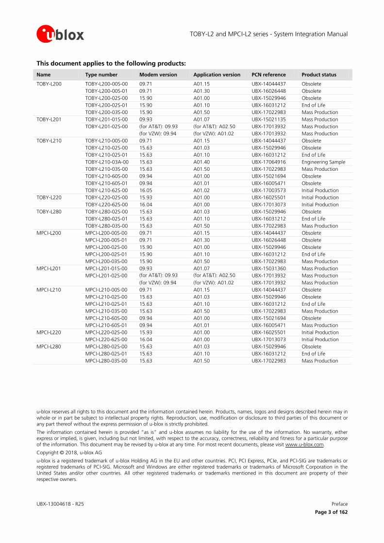
This document applies to the following products:
Name Type number Modem version Application version PCN reference Product status
TOBY-L200 TOBY-L200-00S-00 09.71 A01.15 UBX-14044437 Obsolete
TOBY-L200-00S-01 09.71 A01.30 UBX-16026448 Obsolete
TOBY-L200-02S-00 15.90 A01.00 UBX-15029946 Obsolete
TOBY-L200-02S-01 15.90 A01.10 UBX-16031212 End of Life
TOBY-L200-03S-00 15.90 A01.50 UBX-17022983 Mass Production
TOBY-L201 TOBY-L201-01S-00 09.93 A01.07 UBX-15021135 Mass Production
TOBY-L201-02S-00 (for AT&T): 09.93 (for AT&T): A02.50 UBX-17013932 Mass Production
(for VZW): 09.94 (for VZW): A01.02 UBX-17013932 Mass Production
TOBY-L210 TOBY-L210-00S-00 09.71 A01.15 UBX-14044437 Obsolete
TOBY-L210-02S-00 15.63 A01.03 UBX-15029946 Obsolete
TOBY-L210-02S-01 15.63 A01.10 UBX-16031212 End of Life
TOBY-L210-03A-00 15.63 A01.40 UBX-17064916 Engineering Sample
TOBY-L210-03S-00 15.63 A01.50 UBX-17022983 Mass Production
TOBY-L210-60S-00 09.94 A01.00 UBX-15021694 Obsolete
TOBY-L210-60S-01 09.94 A01.01 UBX-16005471 Obsolete
TOBY-L210-62S-00 16.05 A01.02 UBX-17003573 Initial Production
TOBY-L220 TOBY-L220-02S-00 15.93 A01.00 UBX-16025501 Initial Production
TOBY-L220-62S-00 16.04 A01.00 UBX-17013073 Initial Production
TOBY-L280 TOBY-L280-02S-00 15.63 A01.03 UBX-15029946 Obsolete
TOBY-L280-02S-01 15.63 A01.10 UBX-16031212 End of Life
TOBY-L280-03S-00 15.63 A01.50 UBX-17022983 Mass Production
MPCI-L200 MPCI-L200-00S-00 09.71 A01.15 UBX-14044437 Obsolete
MPCI-L200-00S-01 09.71 A01.30 UBX-16026448 Obsolete
MPCI-L200-02S-00 15.90 A01.00 UBX-15029946 Obsolete
MPCI-L200-02S-01 15.90 A01.10 UBX-16031212 End of Life
MPCI-L200-03S-00 15.90 A01.50 UBX-17022983 Mass Production
MPCI-L201 MPCI-L201-01S-00 09.93 A01.07 UBX-15031360 Mass Production
MPCI-L201-02S-00 (for AT&T): 09.93 (for AT&T): A02.50 UBX-17013932 Mass Production
(for VZW): 09.94 (for VZW): A01.02 UBX-17013932 Mass Production
MPCI-L210 MPCI-L210-00S-00 09.71 A01.15 UBX-14044437 Obsolete
MPCI-L210-02S-00 15.63 A01.03 UBX-15029946 Obsolete
MPCI-L210-02S-01 15.63 A01.10 UBX-16031212 End of Life
MPCI-L210-03S-00 15.63 A01.50 UBX-17022983 Mass Production
MPCI-L210-60S-00 09.94 A01.00 UBX-15021694 Obsolete
MPCI-L210-60S-01 09.94 A01.01 UBX-16005471 Mass Production
MPCI-L220 MPCI-L220-02S-00 15.93 A01.00 UBX-16025501 Initial Production
MPCI-L220-62S-00 16.04 A01.00 UBX-17013073 Initial Production
MPCI-L280 MPCI-L280-02S-00 15.63 A01.03 UBX-15029946 Obsolete
MPCI-L280-02S-01 15.63 A01.10 UBX-16031212 End of Life
MPCI-L280-03S-00 15.63 A01.50 UBX-17022983 Mass Production
u-blox reserves all rights to this document and the information contained herein. Products, names, logos and designs described herein may in
whole or in part be subject to intellectual property rights. Reproduction, use, modification or disclosure to third parties of this document or any part thereof without the express permission of u-blox is strictly prohibited.
The information contained herein is provided “as is” and u-blox assumes no liability for the use of the information. No warranty, either express or implied, is given, including but not limited, with respect to the accuracy, correctness, reliability and fitness for a particular purpose
of the information. This document may be revised by u-blox at any time. For most recent documents, please visit www.u-blox.com.
Copyright © 2018, u-blox AG
u-blox is a registered trademark of u-blox Holding AG in the EU and other countries. PCI, PCI Express, PCIe, and PCI-SIG are trademarks or registered trademarks of PCI-SIG. Microsoft and Windows are either registered trademarks or trademarks of Microsoft Corporation in the
United States and/or other countries. All other registered trademarks or trademarks mentioned in this document are property of their respective owners.
TOBY-L2 and MPCI-L2 series - System Integration Manual
UBX-13004618 - R25 Preface
Page 4 of 162
Preface u-blox Technical Documentation As part of our commitment to customer support, u-blox maintains an extensive volume of technical documentation for our products. In addition to our product-specific technical data sheets, the following manuals are available to assist u-blox customers in product design and development.
AT Commands Manual: This document provides the description of the AT commands supported by the u-blox cellular modules.
System Integration Manual: This document provides the description of u-blox cellular modules’ system from the hardware and the software point of view, it provides hardware design guidelines for the optimal integration of the cellular modules in the application device and it provides information on how to set up production and final product tests on application devices integrating the cellular modules.
Application Note: These documents provide guidelines and information on specific hardware and/or software topics on u-blox cellular modules. See Related documents for a list of Application Notes related to your Cellular Module.
How to use this Manual The TOBY-L2 and MPCI-L2 series System Integration Manual provides the necessary information to successfully design and configure the u-blox cellular modules.
This manual has a modular structure. It is not necessary to read it from the beginning to the end.
The following symbols are used to highlight important information within the manual:
An index finger points out key information pertaining to module integration and performance.
A warning symbol indicates actions that could negatively impact or damage the module.
Questions If you have any questions about u-blox Cellular Integration:
Read this manual carefully.
Contact our information service on the homepage http://www.u-blox.com/
Technical Support
Worldwide Web
Our website (http://www.u-blox.com/) is a rich pool of information. Product information, technical documents can be accessed 24h a day.
By E-mail
Contact the closest Technical Support office by email. Use our service pool email addresses rather than any personal email address of our staff. This makes sure that your request is processed as soon as possible. You will find the contact details at the end of the document.
Helpful Information when Contacting Technical Support
When contacting Technical Support, have the following information ready:
Module type (TOBY-L200) and firmware version
Module configuration
Clear description of your question or the problem
A short description of the application
Your complete contact details
TOBY-L2 and MPCI-L2 series - System Integration Manual
UBX-13004618 - R25 Contents
Page 5 of 162
Contents
Preface ................................................................................................................................ 4
Contents .............................................................................................................................. 5
1 System description ....................................................................................................... 9
1.1 Overview .............................................................................................................................................. 9
1.2 Architecture ........................................................................................................................................ 12
1.2.1 Internal blocks ............................................................................................................................. 13
1.3 Pin-out ............................................................................................................................................... 14
1.3.1 TOBY-L2 series pin assignment .................................................................................................... 14
1.3.2 MPCI-L2 series pin assignment .................................................................................................... 19
1.4 Operating modes ................................................................................................................................ 21
1.5 Supply interfaces ................................................................................................................................ 23
1.5.1 Module supply input (VCC or 3.3Vaux) ....................................................................................... 23
1.5.2 RTC supply input/output (V_BCKP) .............................................................................................. 30
1.5.3 Generic digital interfaces supply output (V_INT) ........................................................................... 31
1.6 System function interfaces .................................................................................................................. 32
1.6.1 Module power-on ....................................................................................................................... 32
1.6.2 Module power-off ....................................................................................................................... 34
1.6.3 Module reset ............................................................................................................................... 36
1.6.4 Module configuration selection by host processor ....................................................................... 36
1.7 Antenna interface ............................................................................................................................... 37
1.7.1 Antenna RF interfaces (ANT1 / ANT2) .......................................................................................... 37
1.7.2 Antenna detection interface (ANT_DET) ...................................................................................... 40
1.8 SIM interface ...................................................................................................................................... 40
1.8.1 SIM interface ............................................................................................................................... 40
1.8.2 SIM detection interface ............................................................................................................... 40
1.9 Data communication interfaces .......................................................................................................... 41
1.9.1 Universal Serial Bus (USB) ............................................................................................................ 41
1.9.2 Asynchronous serial interface (UART) .......................................................................................... 45
1.9.3 DDC (I2C) interface ...................................................................................................................... 56
1.9.4 Secure Digital Input Output interface (SDIO) ................................................................................ 56
1.10 Audio .............................................................................................................................................. 57
1.10.1 Digital audio over I2S interface ..................................................................................................... 57
1.11 General Purpose Input/Output ........................................................................................................ 58
1.12 Mini PCIe specific signals (W_DISABLE#, LED_WWAN#) .................................................................. 59
1.13 Reserved pins (RSVD) ...................................................................................................................... 59
1.14 Not connected pins (NC) ................................................................................................................. 59
1.15 System features............................................................................................................................... 60
1.15.1 Network indication ...................................................................................................................... 60
1.15.2 Antenna supervisor ..................................................................................................................... 60
TOBY-L2 and MPCI-L2 series - System Integration Manual
UBX-13004618 - R25 Contents
Page 6 of 162
1.15.3 Jamming detection ...................................................................................................................... 60
1.15.4 IP modes of operation ................................................................................................................. 61
1.15.5 Dual stack IPv4/IPv6 ..................................................................................................................... 61
1.15.6 TCP/IP and UDP/IP ....................................................................................................................... 61
1.15.7 FTP .............................................................................................................................................. 61
1.15.8 HTTP ........................................................................................................................................... 62
1.15.9 SSL / TLS ...................................................................................................................................... 62
1.15.10 Bearer Independent Protocol.................................................................................................... 63
1.15.11 Wi-Fi integration ...................................................................................................................... 64
1.15.12 Firmware update Over AT (FOAT) ............................................................................................ 64
1.15.13 Firmware update Over The Air (FOTA) ...................................................................................... 64
1.15.14 Smart temperature management ............................................................................................. 65
1.15.15 SIM Access Profile (SAP) ........................................................................................................... 67
1.15.16 Power saving ........................................................................................................................... 69
2 Design-in ..................................................................................................................... 70
2.1 Overview ............................................................................................................................................ 70
2.2 Supply interfaces ................................................................................................................................ 71
2.2.1 Module supply (VCC or 3.3Vaux) ................................................................................................ 71
2.2.2 RTC supply output (V_BCKP) ....................................................................................................... 83
2.2.3 Generic digital interfaces supply output (V_INT) ........................................................................... 85
2.3 System functions interfaces ................................................................................................................ 86
2.3.1 Module power-on (PWR_ON) ...................................................................................................... 86
2.3.2 Module reset (RESET_N or PERST#) .............................................................................................. 87
2.3.3 Module configuration selection by host processor ....................................................................... 88
2.4 Antenna interface ............................................................................................................................... 89
2.4.1 Antenna RF interfaces (ANT1 / ANT2) .......................................................................................... 89
2.4.2 Antenna detection interface (ANT_DET) ...................................................................................... 97
2.5 SIM interface ...................................................................................................................................... 99
2.5.1 Guidelines for SIM circuit design.................................................................................................. 99
2.5.2 Guidelines for SIM layout design ............................................................................................... 105
2.6 Data communication interfaces ........................................................................................................ 106
2.6.1 Universal Serial Bus (USB) .......................................................................................................... 106
2.6.2 Asynchronous serial interface (UART) ........................................................................................ 108
2.6.3 DDC (I2C) interface .................................................................................................................... 112
2.6.4 Secure Digital Input Output interface (SDIO) .............................................................................. 113
2.7 Audio interface ................................................................................................................................. 115
2.7.1 Digital audio interface ............................................................................................................... 115
2.8 General Purpose Input/Output .......................................................................................................... 119
2.9 Mini PCIe specific signals (W_DISABLE#, LED_WWAN#) .................................................................... 120
2.10 Reserved pins (RSVD) .................................................................................................................... 121
2.11 Module placement ........................................................................................................................ 122
2.12 TOBY-L2 series module footprint and paste mask ......................................................................... 123
2.13 MPCI-L2 series module installation ................................................................................................ 124
TOBY-L2 and MPCI-L2 series - System Integration Manual
UBX-13004618 - R25 Contents
Page 7 of 162
2.14 Thermal guidelines ........................................................................................................................ 126
2.15 ESD guidelines .............................................................................................................................. 127
2.15.1 ESD immunity test overview ...................................................................................................... 127
2.15.2 ESD immunity test of TOBY-L2 and MPCI-L2 series reference designs ........................................ 128
2.15.3 ESD application circuits .............................................................................................................. 128
2.16 Schematic for TOBY-L2 and MPCI-L2 series module integration .................................................... 130
2.16.1 Schematic for TOBY-L2 module “00” product version ............................................................... 130
2.16.2 Schematic for TOBY-L2 module “01” or “60” product versions ................................................ 131
2.16.3 Schematic for TOBY-L2 module “02”, “03” or “62” product versions ...................................... 132
2.16.4 Schematic for MPCI-L2 series ..................................................................................................... 133
2.17 Design-in checklist ........................................................................................................................ 134
2.17.1 Schematic checklist ................................................................................................................... 134
2.17.2 Layout checklist ......................................................................................................................... 135
2.17.3 Antenna checklist ...................................................................................................................... 135
3 Handling and soldering ........................................................................................... 136
3.1 Packaging, shipping, storage and moisture preconditioning ............................................................. 136
3.2 Handling ........................................................................................................................................... 136
3.3 Soldering .......................................................................................................................................... 137
3.3.1 Soldering paste ......................................................................................................................... 137
3.3.2 Reflow soldering ....................................................................................................................... 137
3.3.3 Optical inspection ...................................................................................................................... 138
3.3.4 Cleaning .................................................................................................................................... 138
3.3.5 Repeated reflow soldering ......................................................................................................... 139
3.3.6 Wave soldering ......................................................................................................................... 139
3.3.7 Hand soldering .......................................................................................................................... 139
3.3.8 Rework ...................................................................................................................................... 139
3.3.9 Conformal coating .................................................................................................................... 139
3.3.10 Casting ...................................................................................................................................... 139
3.3.11 Grounding metal covers ............................................................................................................ 139
3.3.12 Use of ultrasonic processes ........................................................................................................ 139
4 Approvals .................................................................................................................. 140
4.1 Product certification approval overview............................................................................................. 140
4.2 US Federal Communications Commission notice ............................................................................... 141
4.2.1 Safety warnings review the structure ......................................................................................... 141
4.2.2 Declaration of Conformity ......................................................................................................... 141
4.2.3 Modifications ............................................................................................................................ 142
4.3 Innovation, Science and Economic Development Canada notice ....................................................... 142
4.3.1 Declaration of Conformity ......................................................................................................... 143
4.3.2 Modifications ............................................................................................................................ 143
4.4 Brazilian Anatel certification ............................................................................................................. 145
4.5 European Conformance CE mark ...................................................................................................... 146
4.6 Australian Regulatory Compliance Mark ........................................................................................... 147
4.7 Taiwanese NCC certification ............................................................................................................. 147
TOBY-L2 and MPCI-L2 series - System Integration Manual
UBX-13004618 - R25 Contents
Page 8 of 162
4.8 Japanese Giteki certification ............................................................................................................. 148
5 Product testing ......................................................................................................... 149
5.1 u-blox in-series production test ......................................................................................................... 149
5.2 Test parameters for OEM manufacturer ............................................................................................ 150
5.2.1 “Go/No go” tests for integrated devices .................................................................................... 150
5.2.2 RF functional tests ..................................................................................................................... 150
Appendix ........................................................................................................................ 152
A Migration between TOBY-L1 and TOBY-L2 ............................................................ 152
A.1 Overview .......................................................................................................................................... 152
A.2 Pin-out comparison between TOBY-L1 and TOBY-L2 ........................................................................ 154
A.3 Schematic for TOBY-L1 and TOBY-L2 integration .............................................................................. 156
B Glossary .................................................................................................................... 157
Related documents ........................................................................................................ 159
Revision history .............................................................................................................. 160
Contact ............................................................................................................................ 162
TOBY-L2 and MPCI-L2 series - System Integration Manual
UBX-13004618 - R25 System description
Page 9 of 162
1 System description
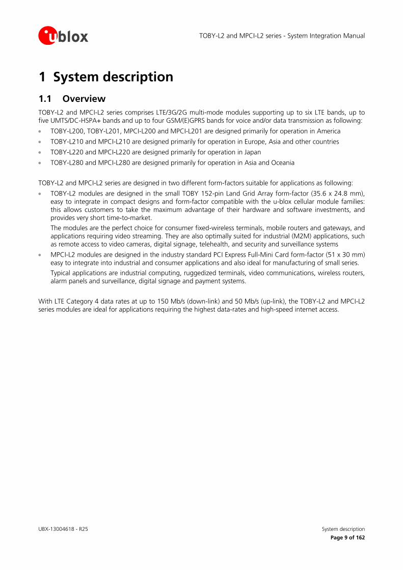
1.1 Overview
TOBY-L2 and MPCI-L2 series comprises LTE/3G/2G multi-mode modules supporting up to six LTE bands, up to five UMTS/DC-HSPA+ bands and up to four GSM/(E)GPRS bands for voice and/or data transmission as following:
TOBY-L200, TOBY-L201, MPCI-L200 and MPCI-L201 are designed primarily for operation in America
TOBY-L210 and MPCI-L210 are designed primarily for operation in Europe, Asia and other countries
TOBY-L220 and MPCI-L220 are designed primarily for operation in Japan
TOBY-L280 and MPCI-L280 are designed primarily for operation in Asia and Oceania
TOBY-L2 and MPCI-L2 series are designed in two different form-factors suitable for applications as following:
TOBY-L2 modules are designed in the small TOBY 152-pin Land Grid Array form-factor (35.6 x 24.8 mm), easy to integrate in compact designs and form-factor compatible with the u-blox cellular module families: this allows customers to take the maximum advantage of their hardware and software investments, and provides very short time-to-market.
The modules are the perfect choice for consumer fixed-wireless terminals, mobile routers and gateways, and applications requiring video streaming. They are also optimally suited for industrial (M2M) applications, such as remote access to video cameras, digital signage, telehealth, and security and surveillance systems
MPCI-L2 modules are designed in the industry standard PCI Express Full-Mini Card form-factor (51 x 30 mm) easy to integrate into industrial and consumer applications and also ideal for manufacturing of small series.
Typical applications are industrial computing, ruggedized terminals, video communications, wireless routers, alarm panels and surveillance, digital signage and payment systems.
With LTE Category 4 data rates at up to 150 Mb/s (down-link) and 50 Mb/s (up-link), the TOBY-L2 and MPCI-L2 series modules are ideal for applications requiring the highest data-rates and high-speed internet access.
TOBY-L2 and MPCI-L2 series - System Integration Manual
UBX-13004618 - R25 System description
Page 10 of 162
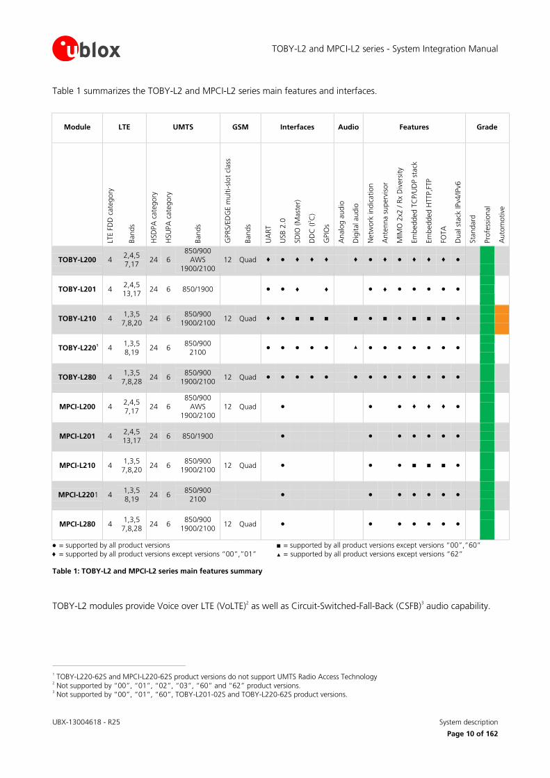
Table 1 summarizes the TOBY-L2 and MPCI-L2 series main features and interfaces.
Module LTE UMTS GSM Interfaces Audio Features Grade
LTE F
DD
cate
gory
Bands
HSD
PA
cate
gory
HSU
PA
cate
gory
Bands
GPRS/E
DG
E m
ult
i-sl
ot
class
Bands
UA
RT
USB 2
.0
SD
IO (M
ast
er)
DD
C (I2C
)
GPIO
s
Analo
g a
udio
Dig
ital audio
Netw
ork
indic
ation
Ante
nna s
uperv
iso
r
MIM
O 2
x2 /
Rx
Div
ers
ity
Em
bedded T
CP/U
DP s
tack
Em
bedded H
TTP,F
TP
FOTA
Dual st
ack
IPv4
/IPv6
Sta
ndard
Pro
fess
ional
Auto
moti
ve
TOBY-L200 4 2,4,5 7,17
24 6 850/900
AWS
1900/2100
12 Quad ♦ ● ♦ ♦ ♦ ♦ ● ♦ ● ♦ ♦ ♦ ●
TOBY-L201 4 2,4,5 13,17
24 6 850/1900 ● ● ♦ ♦ ● ♦ ● ● ● ● ●
TOBY-L210 4 1,3,5
7,8,20 24 6
850/900
1900/2100 12 Quad ♦ ● ■ ■ ■ ■ ● ■ ● ■ ■ ■ ●
TOBY-L2201 4
1,3,5 8,19
24 6 850/900
2100 ● ● ● ● ● ▲ ● ● ● ● ● ● ●
TOBY-L280 4 1,3,5
7,8,28 24 6
850/900 1900/2100
12 Quad ● ● ● ● ● ● ● ● ● ● ● ● ●
MPCI-L200 4 2,4,5
7,17 24 6
850/900
AWS 1900/2100
12 Quad ● ● ● ♦ ♦ ♦ ●
MPCI-L201 4 2,4,5
13,17 24 6 850/1900 ● ● ● ● ● ● ●
MPCI-L210 4 1,3,5
7,8,20 24 6
850/900 1900/2100
12 Quad ● ● ● ■ ■ ■ ●
MPCI-L2201 4 1,3,5
8,19 24 6
850/900
2100 ● ● ● ● ● ● ●
MPCI-L280 4 1,3,5
7,8,28 24 6
850/900
1900/2100 12 Quad ● ● ● ● ● ● ●
● = supported by all product versions
♦ = supported by all product versions except versions “00”,”01”
■ = supported by all product versions except versions “00”,”60”
▲ = supported by all product versions except versions “62”
Table 1: TOBY-L2 and MPCI-L2 series main features summary
TOBY-L2 modules provide Voice over LTE (VoLTE)2 as well as Circuit-Switched-Fall-Back (CSFB)
3 audio capability.
1 TOBY-L220-62S and MPCI-L220-62S product versions do not support UMTS Radio Access Technology
2 Not supported by “00”, “01”, “02”, “03”, “60” and “62” product versions.
3 Not supported by “00”, “01”, “60”, TOBY-L201-02S and TOBY-L220-62S product versions.
TOBY-L2 and MPCI-L2 series - System Integration Manual
UBX-13004618 - R25 System description
Page 11 of 162
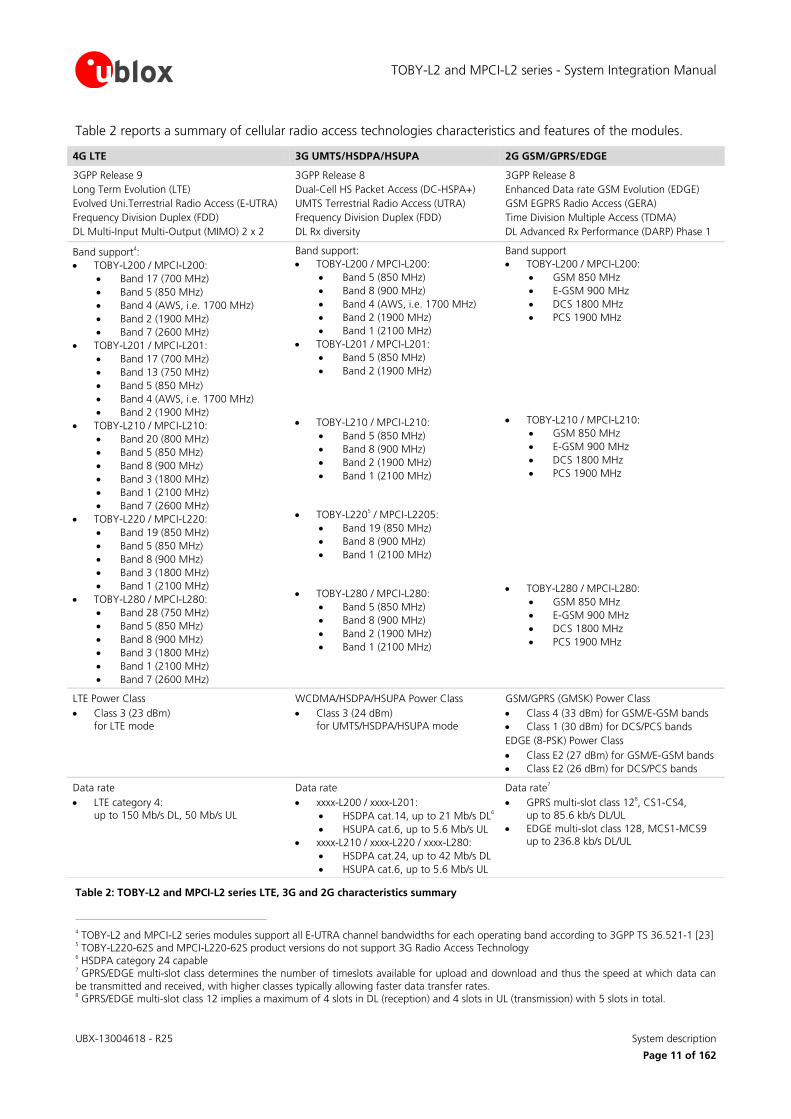
Table 2 reports a summary of cellular radio access technologies characteristics and features of the modules.
4G LTE 3G UMTS/HSDPA/HSUPA 2G GSM/GPRS/EDGE
3GPP Release 9
Long Term Evolution (LTE)
Evolved Uni.Terrestrial Radio Access (E-UTRA)
Frequency Division Duplex (FDD)
DL Multi-Input Multi-Output (MIMO) 2 x 2
3GPP Release 8
Dual-Cell HS Packet Access (DC-HSPA+)
UMTS Terrestrial Radio Access (UTRA)
Frequency Division Duplex (FDD)
DL Rx diversity
3GPP Release 8
Enhanced Data rate GSM Evolution (EDGE)
GSM EGPRS Radio Access (GERA)
Time Division Multiple Access (TDMA)
DL Advanced Rx Performance (DARP) Phase 1
Band support4:
TOBY-L200 / MPCI-L200:
Band 17 (700 MHz)
Band 5 (850 MHz)
Band 4 (AWS, i.e. 1700 MHz)
Band 2 (1900 MHz)
Band 7 (2600 MHz)
TOBY-L201 / MPCI-L201:
Band 17 (700 MHz)
Band 13 (750 MHz)
Band 5 (850 MHz)
Band 4 (AWS, i.e. 1700 MHz)
Band 2 (1900 MHz)
TOBY-L210 / MPCI-L210:
Band 20 (800 MHz)
Band 5 (850 MHz)
Band 8 (900 MHz)
Band 3 (1800 MHz)
Band 1 (2100 MHz)
Band 7 (2600 MHz)
TOBY-L220 / MPCI-L220:
Band 19 (850 MHz)
Band 5 (850 MHz)
Band 8 (900 MHz)
Band 3 (1800 MHz)
Band 1 (2100 MHz)
TOBY-L280 / MPCI-L280:
Band 28 (750 MHz)
Band 5 (850 MHz)
Band 8 (900 MHz)
Band 3 (1800 MHz)
Band 1 (2100 MHz)
Band 7 (2600 MHz)
Band support:
TOBY-L200 / MPCI-L200:
Band 5 (850 MHz)
Band 8 (900 MHz)
Band 4 (AWS, i.e. 1700 MHz)
Band 2 (1900 MHz)
Band 1 (2100 MHz)
TOBY-L201 / MPCI-L201:
Band 5 (850 MHz)
Band 2 (1900 MHz)
TOBY-L210 / MPCI-L210:
Band 5 (850 MHz)
Band 8 (900 MHz)
Band 2 (1900 MHz)
Band 1 (2100 MHz)
TOBY-L2205 / MPCI-L2205:
Band 19 (850 MHz)
Band 8 (900 MHz)
Band 1 (2100 MHz)
TOBY-L280 / MPCI-L280:
Band 5 (850 MHz)
Band 8 (900 MHz)
Band 2 (1900 MHz)
Band 1 (2100 MHz)
Band support
TOBY-L200 / MPCI-L200:
GSM 850 MHz
E-GSM 900 MHz
DCS 1800 MHz
PCS 1900 MHz
TOBY-L210 / MPCI-L210:
GSM 850 MHz
E-GSM 900 MHz
DCS 1800 MHz
PCS 1900 MHz
TOBY-L280 / MPCI-L280:
GSM 850 MHz
E-GSM 900 MHz
DCS 1800 MHz
PCS 1900 MHz
LTE Power Class
Class 3 (23 dBm)
for LTE mode
WCDMA/HSDPA/HSUPA Power Class
Class 3 (24 dBm)
for UMTS/HSDPA/HSUPA mode
GSM/GPRS (GMSK) Power Class
Class 4 (33 dBm) for GSM/E-GSM bands
Class 1 (30 dBm) for DCS/PCS bands
EDGE (8-PSK) Power Class
Class E2 (27 dBm) for GSM/E-GSM bands
Class E2 (26 dBm) for DCS/PCS bands
Data rate
LTE category 4: up to 150 Mb/s DL, 50 Mb/s UL
Data rate
xxxx-L200 / xxxx-L201:
HSDPA cat.14, up to 21 Mb/s DL6
HSUPA cat.6, up to 5.6 Mb/s UL
xxxx-L210 / xxxx-L220 / xxxx-L280:
HSDPA cat.24, up to 42 Mb/s DL
HSUPA cat.6, up to 5.6 Mb/s UL
Data rate7
GPRS multi-slot class 128, CS1-CS4,
up to 85.6 kb/s DL/UL
EDGE multi-slot class 128, MCS1-MCS9 up to 236.8 kb/s DL/UL
Table 2: TOBY-L2 and MPCI-L2 series LTE, 3G and 2G characteristics summary
4 TOBY-L2 and MPCI-L2 series modules support all E-UTRA channel bandwidths for each operating band according to 3GPP TS 36.521-1 [23]
5 TOBY-L220-62S and MPCI-L220-62S product versions do not support 3G Radio Access Technology
6 HSDPA category 24 capable
7 GPRS/EDGE multi-slot class determines the number of timeslots available for upload and download and thus the speed at which data can
be transmitted and received, with higher classes typically allowing faster data transfer rates. 8 GPRS/EDGE multi-slot class 12 implies a maximum of 4 slots in DL (reception) and 4 slots in UL (transmission) with 5 slots in total.
TOBY-L2 and MPCI-L2 series - System Integration Manual
UBX-13004618 - R25 System description
Page 12 of 162
1.2 Architecture
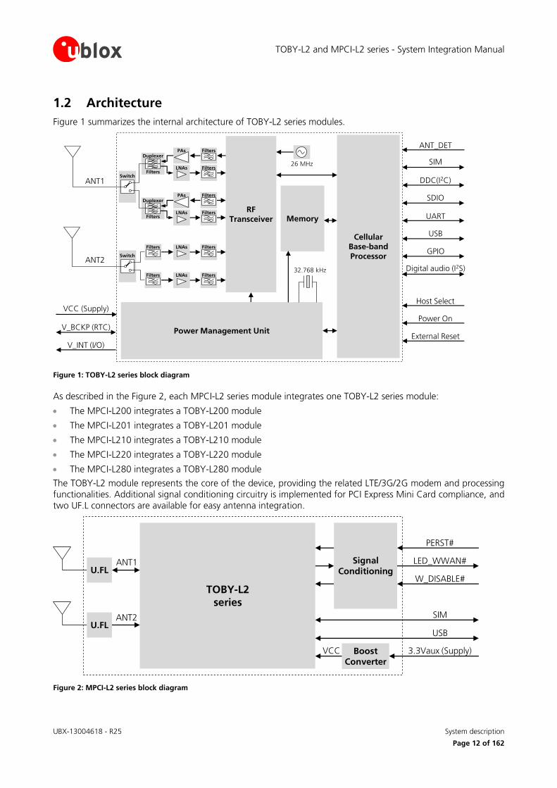
Figure 1 summarizes the internal architecture of TOBY-L2 series modules.
CellularBase-band
Processor
Memory
Power Management Unit
26 MHz
32.768 kHz
ANT1
RF Transceiver
ANT2
V_INT (I/O)
V_BCKP (RTC)
VCC (Supply)
SIM
USB
GPIO
Power On
External Reset
PAs
LNAs Filters
FiltersDuplexer
Filters
PAs
LNAs Filters
FiltersDuplexer
Filters
LNAs FiltersFilters
LNAs FiltersFilters
Switch
Switch
DDC(I2C)
SDIO
UART
Digital audio (I2S)
ANT_DET
Host Select
Figure 1: TOBY-L2 series block diagram
As described in the Figure 2, each MPCI-L2 series module integrates one TOBY-L2 series module:
The MPCI-L200 integrates a TOBY-L200 module
The MPCI-L201 integrates a TOBY-L201 module
The MPCI-L210 integrates a TOBY-L210 module
The MPCI-L220 integrates a TOBY-L220 module
The MPCI-L280 integrates a TOBY-L280 module
The TOBY-L2 module represents the core of the device, providing the related LTE/3G/2G modem and processing functionalities. Additional signal conditioning circuitry is implemented for PCI Express Mini Card compliance, and two UF.L connectors are available for easy antenna integration.
ANT1
SIM
USB
W_DISABLE#
TOBY-L2series
Signal Conditioning
ANT2
PERST#
LED_WWAN#U.FL
U.FL
3.3Vaux (Supply)Boost Converter
VCC
Figure 2: MPCI-L2 series block diagram
TOBY-L2 and MPCI-L2 series - System Integration Manual
UBX-13004618 - R25 System description
Page 13 of 162
1.2.1 Internal blocks
As described in Figure 2, each MPCI-L2 series module integrates one TOBY-L2 series module, which consists of the following internal sections: RF, baseband and power management.
RF section
The RF section is composed of RF transceiver, PAs, LNAs, crystal oscillator, filters, duplexers and RF switches.
Tx signal is pre-amplified by RF transceiver, then output to the primary antenna input/output port (ANT1) of the module via power amplifier (PA), SAW band pass filters band, specific duplexer and antenna switch.
Dual receiving paths are implemented according to LTE Down-Link MIMO 2 x 2 and 3G Receiver Diversity radio technologies supported by the modules as LTE category 4 and HSDPA category 24 User Equipments: incoming signals are received through the primary (ANT1) and the secondary (ANT2) antenna input ports which are connected to the RF transceiver via specific antenna switch, diplexer, duplexer, LNA, SAW band pass filters.
RF transceiver performs modulation, up-conversion of the baseband I/Q signals for Tx, down-conversion and demodulation of the dual RF signals for Rx. The RF transceiver contains:
Automatically gain controlled direct conversion Zero-IF receiver,
Highly linear RF demodulator / modulator capable GMSK, 8-PSK, QPSK, 16-QAM, 64-QAM,
Fractional-N Sigma-Delta RF synthesizer,
VCO.
Power Amplifiers (PA) amplify the Tx signal modulated by the RF transceiver
RF switches connect primary (ANT1) and secondary (ANT2) antenna ports to the suitable Tx / Rx path
Low Noise Amplifiers (LNA) enhance the received sensitivity
SAW duplexers separate the Tx and Rx signal paths and provide RF filtering
SAW band pass filters enhance the rejection of out-of-band signals
26 MHz crystal oscillator generates the clock reference in active-mode or connected-mode.
Baseband and power management section
The Baseband and Power Management section is composed of the following main elements:
A mixed signal ASIC, which integrates
Microprocessor for control functions
DSP core for LTE/3G/2G Layer 1 and digital processing of Rx and Tx signal paths
Memory interface controller
Dedicated peripheral blocks for control of the USB, SIM and GPIO digital interfaces
Analog front end interfaces to RF transceiver ASIC
Memory system, which includes NAND flash and LPDDR
Voltage regulators to derive all the subsystem supply voltages from the module supply input VCC
Voltage sources for external use: V_BCKP and V_INT (not available on MPCI-L2 series modules)
Hardware power on
Hardware reset
Low power idle-mode support
32.768 kHz crystal oscillator to provide the clock reference in the low power idle-mode, which can be set by enable power saving configuration using the AT+UPSV command.
TOBY-L2 and MPCI-L2 series - System Integration Manual
UBX-13004618 - R25 System description
Page 14 of 162
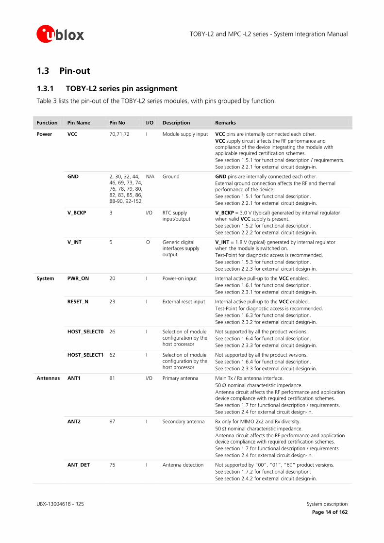
1.3 Pin-out
1.3.1 TOBY-L2 series pin assignment
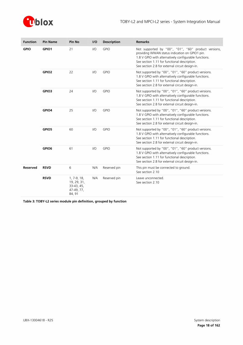
Table 3 lists the pin-out of the TOBY-L2 series modules, with pins grouped by function.
Function Pin Name Pin No I/O Description Remarks
Power VCC 70,71,72 I Module supply input VCC pins are internally connected each other.
VCC supply circuit affects the RF performance and compliance of the device integrating the module with applicable required certification schemes.
See section 1.5.1 for functional description / requirements.
See section 2.2.1 for external circuit design-in.
GND 2, 30, 32, 44, 46, 69, 73, 74,
76, 78, 79, 80, 82, 83, 85, 86, 88-90, 92-152
N/A Ground GND pins are internally connected each other.
External ground connection affects the RF and thermal performance of the device.
See section 1.5.1 for functional description.
See section 2.2.1 for external circuit design-in.
V_BCKP 3 I/O RTC supply input/output
V_BCKP = 3.0 V (typical) generated by internal regulator when valid VCC supply is present.
See section 1.5.2 for functional description.
See section 2.2.2 for external circuit design-in.
V_INT 5 O Generic digital interfaces supply
output
V_INT = 1.8 V (typical) generated by internal regulator when the module is switched on.
Test-Point for diagnostic access is recommended.
See section 1.5.3 for functional description.
See section 2.2.3 for external circuit design-in.
System PWR_ON 20 I Power-on input Internal active pull-up to the VCC enabled.
See section 1.6.1 for functional description.
See section 2.3.1 for external circuit design-in.
RESET_N 23 I External reset input Internal active pull-up to the VCC enabled.
Test-Point for diagnostic access is recommended.
See section 1.6.3 for functional description.
See section 2.3.2 for external circuit design-in.
HOST_SELECT0 26 I Selection of module configuration by the
host processor
Not supported by all the product versions.
See section 1.6.4 for functional description.
See section 2.3.3 for external circuit design-in.
HOST_SELECT1 62 I Selection of module configuration by the
host processor
Not supported by all the product versions.
See section 1.6.4 for functional description.
See section 2.3.3 for external circuit design-in.
Antennas ANT1 81 I/O Primary antenna Main Tx / Rx antenna interface.
50 nominal characteristic impedance.
Antenna circuit affects the RF performance and application
device compliance with required certification schemes.
See section 1.7 for functional description / requirements.
See section 2.4 for external circuit design-in.
ANT2 87 I Secondary antenna Rx only for MIMO 2x2 and Rx diversity.
50 nominal characteristic impedance.
Antenna circuit affects the RF performance and application device compliance with required certification schemes.
See section 1.7 for functional description / requirements
See section 2.4 for external circuit design-in.
ANT_DET 75 I Antenna detection Not supported by “00”, “01”, “60” product versions.
See section 1.7.2 for functional description.
See section 2.4.2 for external circuit design-in.
TOBY-L2 and MPCI-L2 series - System Integration Manual
UBX-13004618 - R25 System description
Page 15 of 162
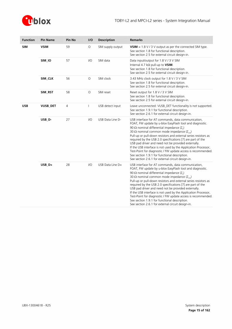
Function Pin Name Pin No I/O Description Remarks
SIM VSIM 59 O SIM supply output VSIM = 1.8 V / 3 V output as per the connected SIM type.
See section 1.8 for functional description. See section 2.5 for external circuit design-in.
SIM_IO 57 I/O SIM data Data input/output for 1.8 V / 3 V SIM
Internal 4.7 k pull-up to VSIM.
See section 1.8 for functional description.
See section 2.5 for external circuit design-in.
SIM_CLK 56 O SIM clock 3.43 MHz clock output for 1.8 V / 3 V SIM
See section 1.8 for functional description.
See section 2.5 for external circuit design-in.
SIM_RST 58 O SIM reset Reset output for 1.8 V / 3 V SIM
See section 1.8 for functional description. See section 2.5 for external circuit design-in.
USB VUSB_DET 4 I USB detect input Leave unconnected: VUSB_DET functionality is not supported.
See section 1.9.1 for functional description.
See section 2.6.1 for external circuit design-in.
USB_D- 27 I/O USB Data Line D- USB interface for AT commands, data communication, FOAT, FW update by u-blox EasyFlash tool and diagnostic.
90 nominal differential impedance (Z0)
30 nominal common mode impedance (ZCM
)
Pull-up or pull-down resistors and external series resistors as required by the USB 2.0 specifications [7] are part of the
USB pad driver and need not be provided externally.
If the USB interface is not used by the Application Processor, Test-Point for diagnostic / FW update access is recommended.
See section 1.9.1 for functional description.
See section 2.6.1 for external circuit design-in.
USB_D+ 28 I/O USB Data Line D+ USB interface for AT commands, data communication, FOAT, FW update by u-blox EasyFlash tool and diagnostic.
90 nominal differential impedance (Z0)
30 nominal common mode impedance (ZCM
)
Pull-up or pull-down resistors and external series resistors as required by the USB 2.0 specifications [7] are part of the
USB pad driver and need not be provided externally.
If the USB interface is not used by the Application Processor, Test-Point for diagnostic / FW update access is recommended.
See section 1.9.1 for functional description.
See section 2.6.1 for external circuit design-in.
TOBY-L2 and MPCI-L2 series - System Integration Manual
UBX-13004618 - R25 System description
Page 16 of 162
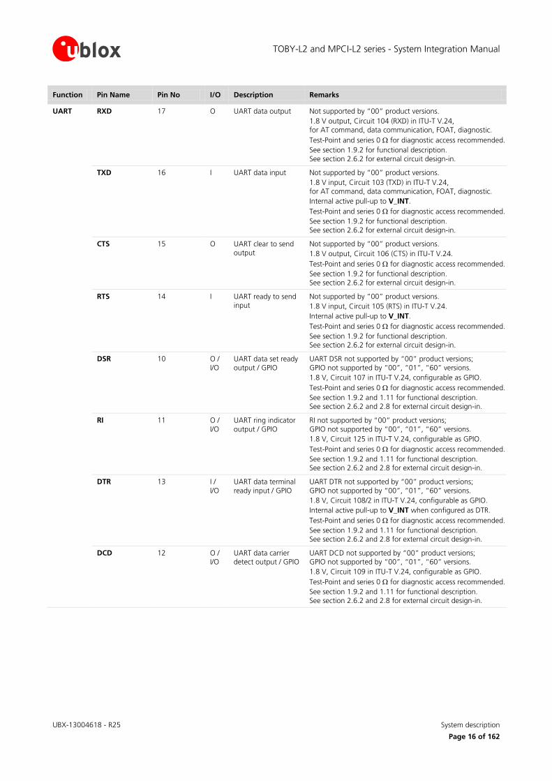
Function Pin Name Pin No I/O Description Remarks
UART RXD 17 O UART data output Not supported by “00” product versions.
1.8 V output, Circuit 104 (RXD) in ITU-T V.24, for AT command, data communication, FOAT, diagnostic.
Test-Point and series 0 for diagnostic access recommended.
See section 1.9.2 for functional description.
See section 2.6.2 for external circuit design-in.
TXD 16 I UART data input Not supported by “00” product versions.
1.8 V input, Circuit 103 (TXD) in ITU-T V.24, for AT command, data communication, FOAT, diagnostic.
Internal active pull-up to V_INT.
Test-Point and series 0 for diagnostic access recommended.
See section 1.9.2 for functional description.
See section 2.6.2 for external circuit design-in.
CTS 15 O UART clear to send output
Not supported by “00” product versions.
1.8 V output, Circuit 106 (CTS) in ITU-T V.24.
Test-Point and series 0 for diagnostic access recommended.
See section 1.9.2 for functional description.
See section 2.6.2 for external circuit design-in.
RTS 14 I UART ready to send input
Not supported by “00” product versions.
1.8 V input, Circuit 105 (RTS) in ITU-T V.24.
Internal active pull-up to V_INT.
Test-Point and series 0 for diagnostic access recommended.
See section 1.9.2 for functional description. See section 2.6.2 for external circuit design-in.
DSR 10 O /
I/O
UART data set ready
output / GPIO
UART DSR not supported by “00” product versions;
GPIO not supported by “00”, “01”, “60” versions.
1.8 V, Circuit 107 in ITU-T V.24, configurable as GPIO.
Test-Point and series 0 for diagnostic access recommended.
See section 1.9.2 and 1.11 for functional description. See section 2.6.2 and 2.8 for external circuit design-in.
RI 11 O /
I/O
UART ring indicator
output / GPIO
RI not supported by “00” product versions;
GPIO not supported by “00”, “01”, “60” versions.
1.8 V, Circuit 125 in ITU-T V.24, configurable as GPIO.
Test-Point and series 0 for diagnostic access recommended.
See section 1.9.2 and 1.11 for functional description. See section 2.6.2 and 2.8 for external circuit design-in.
DTR 13 I /
I/O
UART data terminal
ready input / GPIO
UART DTR not supported by “00” product versions;
GPIO not supported by “00”, “01”, “60” versions.
1.8 V, Circuit 108/2 in ITU-T V.24, configurable as GPIO.
Internal active pull-up to V_INT when configured as DTR.
Test-Point and series 0 for diagnostic access recommended.
See section 1.9.2 and 1.11 for functional description.
See section 2.6.2 and 2.8 for external circuit design-in.
DCD 12 O / I/O
UART data carrier detect output / GPIO
UART DCD not supported by “00” product versions; GPIO not supported by “00”, “01”, “60” versions.
1.8 V, Circuit 109 in ITU-T V.24, configurable as GPIO.
Test-Point and series 0 for diagnostic access recommended.
See section 1.9.2 and 1.11 for functional description.
See section 2.6.2 and 2.8 for external circuit design-in.
TOBY-L2 and MPCI-L2 series - System Integration Manual
UBX-13004618 - R25 System description
Page 17 of 162
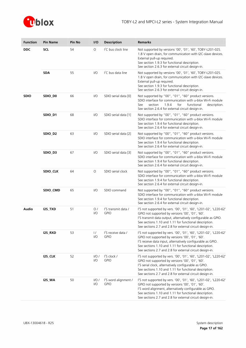
Function Pin Name Pin No I/O Description Remarks
DDC SCL 54 O I2C bus clock line Not supported by versions ‘00’, ‘01’, ‘60’, TOBY-L201-02S.
1.8 V open drain, for communication with I2C-slave devices.
External pull-up required.
See section 1.9.3 for functional description. See section 2.6.3 for external circuit design-in.
SDA 55 I/O I2C bus data line Not supported by versions ‘00’, ‘01’, ‘60’, TOBY-L201-02S.
1.8 V open drain, for communication with I2C-slave devices.
External pull-up required.
See section 1.9.3 for functional description. See section 2.6.3 for external circuit design-in.
SDIO SDIO_D0 66 I/O SDIO serial data [0] Not supported by “00”, “01”, “60” product versions.
SDIO interface for communication with u-blox Wi-Fi module
See section 1.9.4 for functional description.
See section 2.6.4 for external circuit design-in.
SDIO_D1 68 I/O SDIO serial data [1] Not supported by “00”, “01”, “60” product versions.
SDIO interface for communication with u-blox Wi-Fi module
See section 1.9.4 for functional description. See section 2.6.4 for external circuit design-in.
SDIO_D2 63 I/O SDIO serial data [2] Not supported by “00”, “01”, “60” product versions.
SDIO interface for communication with u-blox Wi-Fi module
See section 1.9.4 for functional description.
See section 2.6.4 for external circuit design-in.
SDIO_D3 67 I/O SDIO serial data [3] Not supported by “00”, “01”, “60” product versions.
SDIO interface for communication with u-blox Wi-Fi module
See section 1.9.4 for functional description. See section 2.6.4 for external circuit design-in.
SDIO_CLK 64 O SDIO serial clock Not supported by “00”, “01”, “60” product versions.
SDIO interface for communication with u-blox Wi-Fi module
See section 1.9.4 for functional description.
See section 2.6.4 for external circuit design-in.
SDIO_CMD 65 I/O SDIO command Not supported by “00”, “01”, “60” product versions.
SDIO interface for communication with u-blox Wi-Fi module
See section 1.9.4 for functional description. See section 2.6.4 for external circuit design-in.
Audio I2S_TXD 51 O /
I/O
I2S transmit data /
GPIO
I2S not supported by vers. ‘00’, ‘01’, ‘60’, ‘L201-02’, ‘L220-62’
GPIO not supported by versions ‘00’, ‘01’, ‘60’.
I2S transmit data output, alternatively configurable as GPIO.
See sections 1.10 and 1.11 for functional description.
See sections 2.7 and 2.8 for external circuit design-in.
I2S_RXD 53 I / I/O
I2S receive data /
GPIO
I2S not supported by vers. ‘00’, ‘01’, ‘60’, ‘L201-02’, ‘L220-62’
GPIO not supported by versions ‘00’, ‘01’, ‘60’.
I2S receive data input, alternatively configurable as GPIO.
See sections 1.10 and 1.11 for functional description.
See sections 2.7 and 2.8 for external circuit design-in.
I2S_CLK 52 I/O / I/O
I2S clock /
GPIO
I2S not supported by vers. ‘00’, ‘01’, ‘60’, ‘L201-02’, ‘L220-62’
GPIO not supported by versions ‘00’, ‘01’, ‘60’.
I2S serial clock, alternatively configurable as GPIO.
See sections 1.10 and 1.11 for functional description.
See sections 2.7 and 2.8 for external circuit design-in.
I2S_WA 50 I/O /
I/O
I2S word alignment /
GPIO
I2S not supported by vers. ‘00’, ‘01’, ‘60’, ‘L201-02’, ‘L220-62’
GPIO not supported by versions ‘00’, ‘01’, ‘60’.
I2S word alignment, alternatively configurable as GPIO.
See sections 1.10 and 1.11 for functional description.
See sections 2.7 and 2.8 for external circuit design-in.
TOBY-L2 and MPCI-L2 series - System Integration Manual
UBX-13004618 - R25 System description
Page 18 of 162
Function Pin Name Pin No I/O Description Remarks
GPIO GPIO1 21 I/O GPIO Not supported by “00”, “01”, “60” product versions, providing WWAN status indication on GPIO1 pin.
1.8 V GPIO with alternatively configurable functions.
See section 1.11 for functional description.
See section 2.8 for external circuit design-in.
GPIO2 22 I/O GPIO Not supported by “00”, “01”, “60” product versions.
1.8 V GPIO with alternatively configurable functions.
See section 1.11 for functional description.
See section 2.8 for external circuit design-in.
GPIO3 24 I/O GPIO Not supported by “00”, “01”, “60” product versions.
1.8 V GPIO with alternatively configurable functions.
See section 1.11 for functional description.
See section 2.8 for external circuit design-in.
GPIO4 25 I/O GPIO Not supported by “00”, “01”, “60” product versions.
1.8 V GPIO with alternatively configurable functions.
See section 1.11 for functional description.
See section 2.8 for external circuit design-in.
GPIO5 60 I/O GPIO Not supported by “00”, “01”, “60” product versions.
1.8 V GPIO with alternatively configurable functions.
See section 1.11 for functional description.
See section 2.8 for external circuit design-in.
GPIO6 61 I/O GPIO Not supported by “00”, “01”, “60” product versions.
1.8 V GPIO with alternatively configurable functions.
See section 1.11 for functional description.
See section 2.8 for external circuit design-in.
Reserved RSVD 6 N/A Reserved pin This pin must be connected to ground.
See section 2.10
RSVD 1, 7-9, 18,
19, 29, 31, 33-43, 45,
47-49, 77, 84, 91
N/A Reserved pin Leave unconnected.
See section 2.10
Table 3: TOBY-L2 series module pin definition, grouped by function
TOBY-L2 and MPCI-L2 series - System Integration Manual
UBX-13004618 - R25 System description
Page 19 of 162
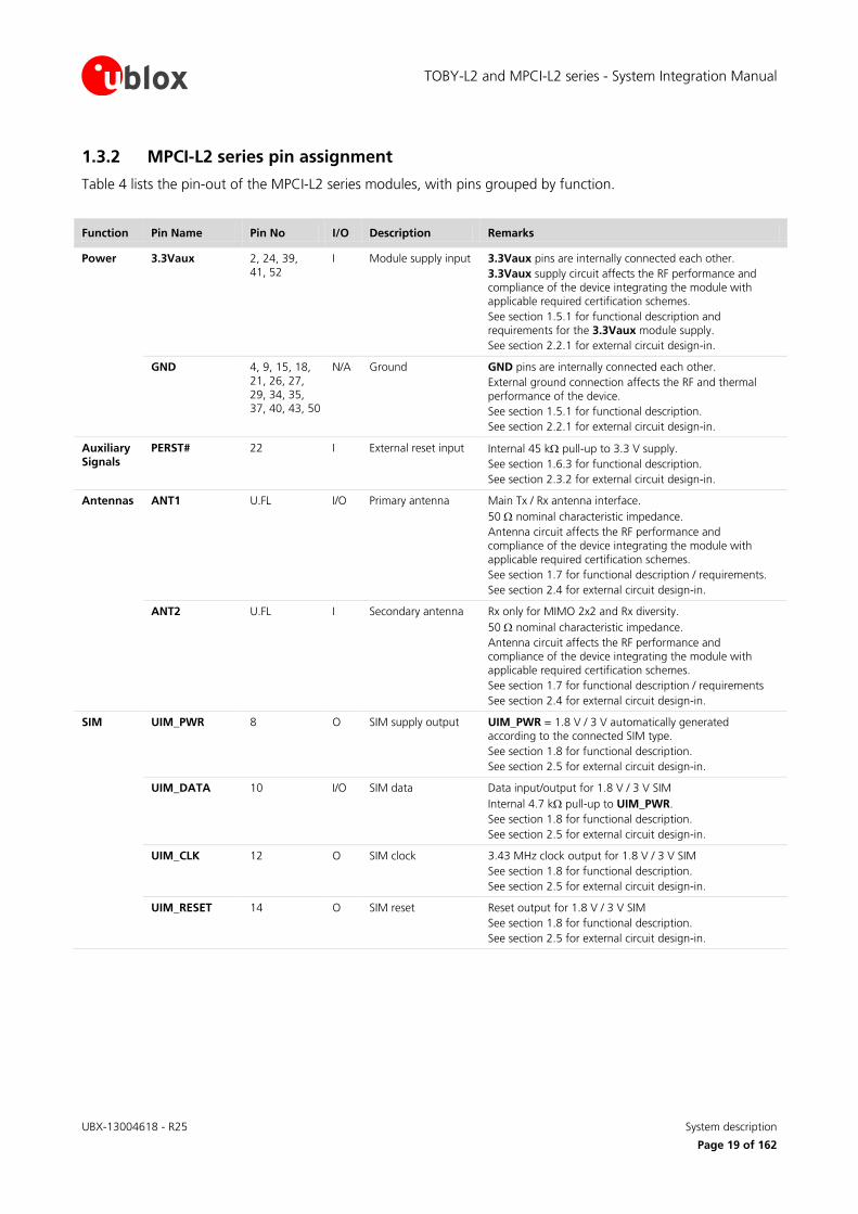
1.3.2 MPCI-L2 series pin assignment
Table 4 lists the pin-out of the MPCI-L2 series modules, with pins grouped by function.
Function Pin Name Pin No I/O Description Remarks
Power 3.3Vaux 2, 24, 39, 41, 52
I Module supply input 3.3Vaux pins are internally connected each other.
3.3Vaux supply circuit affects the RF performance and
compliance of the device integrating the module with applicable required certification schemes.
See section 1.5.1 for functional description and requirements for the 3.3Vaux module supply.
See section 2.2.1 for external circuit design-in.
GND 4, 9, 15, 18, 21, 26, 27,
29, 34, 35, 37, 40, 43, 50
N/A Ground GND pins are internally connected each other.
External ground connection affects the RF and thermal
performance of the device.
See section 1.5.1 for functional description.
See section 2.2.1 for external circuit design-in.
Auxiliary Signals
PERST# 22 I External reset input Internal 45 k pull-up to 3.3 V supply.
See section 1.6.3 for functional description.
See section 2.3.2 for external circuit design-in.
Antennas ANT1 U.FL I/O Primary antenna Main Tx / Rx antenna interface.
50 nominal characteristic impedance.
Antenna circuit affects the RF performance and compliance of the device integrating the module with
applicable required certification schemes.
See section 1.7 for functional description / requirements.
See section 2.4 for external circuit design-in.
ANT2 U.FL I Secondary antenna Rx only for MIMO 2x2 and Rx diversity.
50 nominal characteristic impedance.
Antenna circuit affects the RF performance and compliance of the device integrating the module with
applicable required certification schemes.
See section 1.7 for functional description / requirements
See section 2.4 for external circuit design-in.
SIM UIM_PWR 8 O SIM supply output UIM_PWR = 1.8 V / 3 V automatically generated according to the connected SIM type.
See section 1.8 for functional description.
See section 2.5 for external circuit design-in.
UIM_DATA 10 I/O SIM data Data input/output for 1.8 V / 3 V SIM
Internal 4.7 k pull-up to UIM_PWR.
See section 1.8 for functional description.
See section 2.5 for external circuit design-in.
UIM_CLK 12 O SIM clock 3.43 MHz clock output for 1.8 V / 3 V SIM
See section 1.8 for functional description.
See section 2.5 for external circuit design-in.
UIM_RESET 14 O SIM reset Reset output for 1.8 V / 3 V SIM
See section 1.8 for functional description.
See section 2.5 for external circuit design-in.
TOBY-L2 and MPCI-L2 series - System Integration Manual
UBX-13004618 - R25 System description
Page 20 of 162
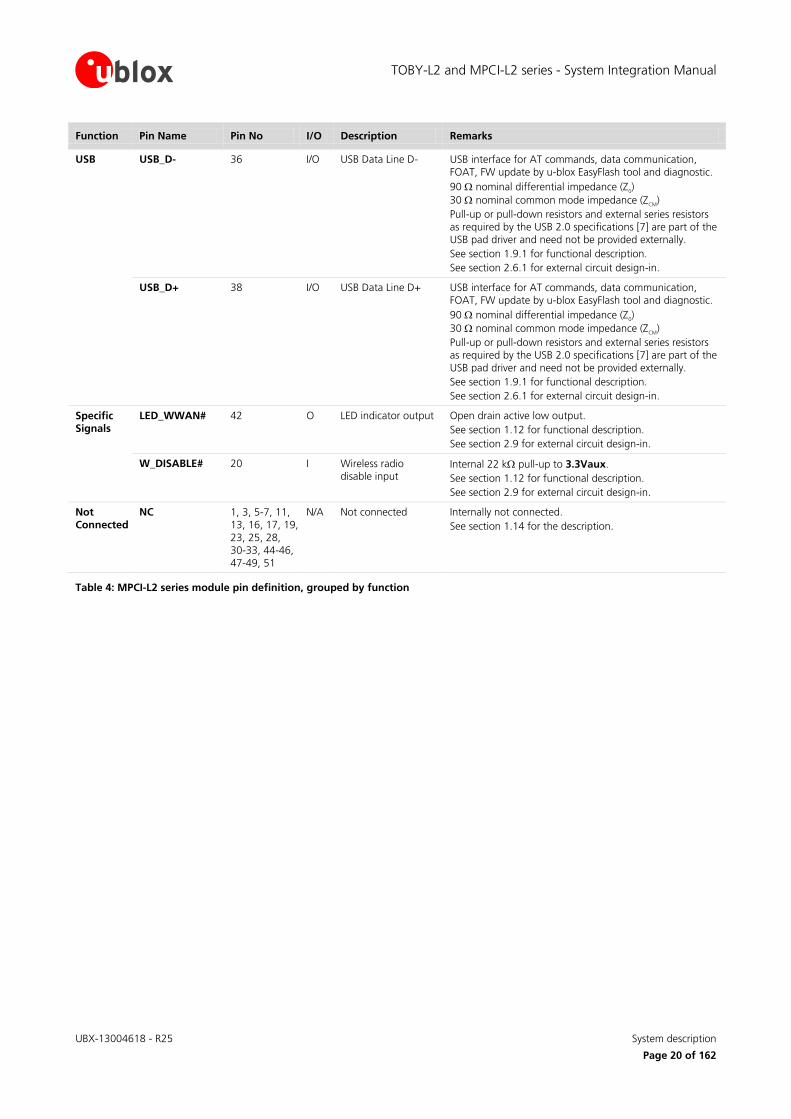
Function Pin Name Pin No I/O Description Remarks
USB USB_D- 36 I/O USB Data Line D- USB interface for AT commands, data communication, FOAT, FW update by u-blox EasyFlash tool and diagnostic.
90 nominal differential impedance (Z0)
30 nominal common mode impedance (ZCM
)
Pull-up or pull-down resistors and external series resistors as required by the USB 2.0 specifications [7] are part of the USB pad driver and need not be provided externally.
See section 1.9.1 for functional description.
See section 2.6.1 for external circuit design-in.
USB_D+ 38 I/O USB Data Line D+ USB interface for AT commands, data communication, FOAT, FW update by u-blox EasyFlash tool and diagnostic.
90 nominal differential impedance (Z0)
30 nominal common mode impedance (ZCM
)
Pull-up or pull-down resistors and external series resistors as required by the USB 2.0 specifications [7] are part of the
USB pad driver and need not be provided externally.
See section 1.9.1 for functional description.
See section 2.6.1 for external circuit design-in.
Specific Signals
LED_WWAN# 42 O LED indicator output Open drain active low output.
See section 1.12 for functional description.
See section 2.9 for external circuit design-in.
W_DISABLE# 20 I Wireless radio disable input
Internal 22 k pull-up to 3.3Vaux.
See section 1.12 for functional description.
See section 2.9 for external circuit design-in.
Not Connected
NC 1, 3, 5-7, 11, 13, 16, 17, 19,
23, 25, 28, 30-33, 44-46,
47-49, 51
N/A Not connected Internally not connected.
See section 1.14 for the description.
Table 4: MPCI-L2 series module pin definition, grouped by function
TOBY-L2 and MPCI-L2 series - System Integration Manual
UBX-13004618 - R25 System description
Page 21 of 162
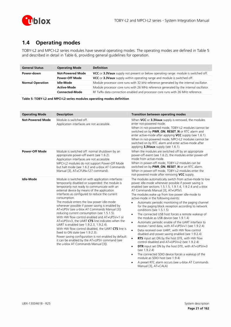
1.4 Operating modes
TOBY-L2 and MPCI-L2 series modules have several operating modes. The operating modes are defined in Table 5 and described in detail in Table 6, providing general guidelines for operation.
General Status Operating Mode Definition
Power-down Not-Powered Mode VCC or 3.3Vaux supply not present or below operating range: module is switched off.
Power-Off Mode VCC or 3.3Vaux supply within operating range and module is switched off.
Normal Operation Idle-Mode Module processor core runs with 32 kHz reference generated by the internal oscillator.
Active-Mode Module processor core runs with 26 MHz reference generated by the internal oscillator.
Connected-Mode RF Tx/Rx data connection enabled and processor core runs with 26 MHz reference.
Table 5: TOBY-L2 and MPCI-L2 series modules operating modes definition
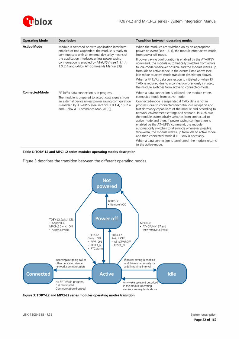
Operating Mode Description Transition between operating modes
Not-Powered Mode Module is switched off.
Application interfaces are not accessible.
When VCC or 3.3Vaux supply is removed, the modules
enter not-powered mode.
When in not-powered mode, TOBY-L2 modules cannot be switched on by PWR_ON, RESET_N or RTC alarm and
enter active-mode after applying VCC supply (see 1.6.1).
When in not-powered mode, MPCI-L2 modules cannot be switched on by RTC alarm and enter active-mode after
applying 3.3Vaux supply (see 1.6.1).
Power-Off Mode Module is switched off: normal shutdown by an appropriate power-off event (see 1.6.2).
Application interfaces are not accessible.
MPCI-L2 modules do not support Power-Off Mode but halt mode (see 1.6.2 and u-blox AT Commands Manual [3], AT+CFUN=127 command).
When the modules are switched off by an appropriate power-off event (see 1.6.2), the modules enter power-off
mode from active-mode.
When in power-off mode, TOBY-L2 modules can be switched on by PWR_ON, RESET_N or an RTC alarm.
When in power-off mode, TOBY-L2 modules enter the
not-powered mode after removing VCC supply.
Idle-Mode Module is switched on with application interfaces
temporarily disabled or suspended: the module is temporarily not ready to communicate with an external device by means of the application
interfaces as configured to reduce the current consumption.
The module enters the low power idle-mode whenever possible if power saving is enabled by AT+UPSV (see u-blox AT Commands Manual [3])
reducing current consumption (see 1.5.1.5).
With HW flow control enabled and AT+UPSV=1 or
AT+UPSV=3, the UART CTS line indicates when the UART is enabled (see 1.9.2.3, 1.9.2.4).
With HW flow control disabled, the UART CTS line is
fixed to ON state (see 1.9.2.3).
Power saving configuration is not enabled by default: it can be enabled by the AT+UPSV command (see
the u-blox AT Commands Manual [3]).
The modules automatically switch from active-mode to low
power idle-mode whenever possible if power saving is enabled (see sections 1.5.1.5, 1.9.1.4, 1.9.2.4 and u-blox AT Commands Manual [3], AT+UPSV).
The modules wake up from low power idle-mode to active-mode in the following events:
Automatic periodic monitoring of the paging channel
for the paging block reception according to network conditions (see 1.5.1.5)
The connected USB host forces a remote wakeup of
the module as USB device (see 1.9.1.4)
Automatic periodic enable of the UART interface to receive / send data, with AT+UPSV=1 (see 1.9.2.4)
Data received over UART, with HW flow control
disabled and power saving enabled (see 1.9.2.4)
RTS input set ON by the host DTE, with HW flow control disabled and AT+UPSV=2 (see 1.9.2.4)
DTR input set ON by the host DTE, with AT+UPSV=3
(see 1.9.2.4)
The connected SDIO device forces a wakeup of the module as SDIO host (see 1.9.4)
A preset RTC alarm occurs (see u-blox AT Commands
Manual [3], AT+CALA)
TOBY-L2 and MPCI-L2 series - System Integration Manual
UBX-13004618 - R25 System description
Page 22 of 162
Operating Mode Description Transition between operating modes
Active-Mode Module is switched on with application interfaces
enabled or not suspended: the module is ready to communicate with an external device by means of
the application interfaces unless power saving configuration is enabled by AT+UPSV (see 1.9.1.4,
1.9.2.4 and u-blox AT Commands Manual [3]).
When the modules are switched on by an appropriate
power-on event (see 1.6.1), the module enter active-mode from power-off mode.
If power saving configuration is enabled by the AT+UPSV command, the module automatically switches from active
to idle-mode whenever possible and the module wakes up from idle to active-mode in the events listed above (see
idle-mode to active-mode transition description above).
When a RF Tx/Rx data connection is initiated or when RF Tx/Rx is required due to a connection previously initiated,
the module switches from active to connected-mode.
Connected-Mode RF Tx/Rx data connection is in progress.
The module is prepared to accept data signals from an external device unless power saving configuration
is enabled by AT+UPSV (see sections 1.9.1.4, 1.9.2.4 and u-blox AT Commands Manual [3]).
When a data connection is initiated, the module enters connected-mode from active-mode.
Connected-mode is suspended if Tx/Rx data is not in
progress, due to connected discontinuous reception and fast dormancy capabilities of the module and according to
network environment settings and scenario. In such case, the module automatically switches from connected to
active mode and then, if power saving configuration is enabled by the AT+UPSV command, the module
automatically switches to idle-mode whenever possible. Vice-versa, the module wakes up from idle to active mode and then connected mode if RF Tx/Rx is necessary.
When a data connection is terminated, the module returns
to the active-mode.
Table 6: TOBY-L2 and MPCI-L2 series modules operating modes description
Figure 3 describes the transition between the different operating modes.
TOBY-L2 Switch ON:• Apply VCCMPCI-L2 Switch ON:• Apply 3.3Vaux
If power saving is enabled and there is no activity for a defined time interval
Any wake up event described in the module operating modes summary table above
Incoming/outgoing call or other dedicated device network communication
No RF Tx/Rx in progress, Call terminated, Communication dropped
TOBY-L2 Switch ON:• PWR_ON• RESET_N• RTC alarm
Not powered
Power off
ActiveConnected Idle
TOBY-L2 Switch OFF:• AT+CPWROFF• RESET_N
MPCI-L2:• AT+CFUN=127 and
then remove 3.3Vaux
TOBY-L2:• Remove VCC
Figure 3: TOBY-L2 and MPCI-L2 series modules operating modes transition
TOBY-L2 and MPCI-L2 series - System Integration Manual
UBX-13004618 - R25 System description
Page 23 of 162
1.5 Supply interfaces
1.5.1 Module supply input (VCC or 3.3Vaux)
TOBY-L2 modules are supplied via the three VCC pins, and MPCI-L2 modules are supplied via the five 3.3Vaux pins. All supply voltages used inside the modules are generated from the VCC or the 3.3Vaux supply input by integrated voltage regulators, including the V_BCKP RTC supply, the V_INT generic digital interface supply, and the VSIM or UIM_PWR SIM interface supply.
The current drawn by the TOBY-L2 and MPCI-L2 series modules through the VCC or 3.3Vaux pins can vary by several orders of magnitude depending on radio access technology, operation mode and state. It is important that the supply source is able to support both the high peak of current consumption during 2G transmission at maximum RF power level (as described in the section 1.5.1.2) and the high average current consumption during 3G and LTE transmission at maximum RF power level (as described in the sections 1.5.1.3 and 1.5.1.4).
1.5.1.1 VCC or 3.3Vaux supply requirements
Table 7 summarizes the requirements for the VCC or 3.3Vaux modules supply. See section 2.2.1 for suggestions to properly design a VCC or 3.3Vaux supply circuit compliant with the requirements listed in Table 7.
The supply circuit affects the RF compliance of the device integrating TOBY-L2 and MPCI-L2 series modules with applicable required certification schemes as well as antenna circuit design. Compliance is guaranteed if the requirements summarized in the Table 7 are fulfilled.
Item Requirement Remark
VCC or 3.3Vaux nominal voltage
Within VCC or 3.3Vaux normal operating range:
See “Supply/Power pins” section in the TOBY-L2 Data Sheet [1] or in the MPCI-L2 Data Sheet [2].
The modules cannot be switched on if the supply voltage is below the normal operating range minimum limit.
VCC or 3.3Vaux voltage during
normal operation
Within VCC or 3.3Vaux extended operating range:
See “Supply/Power pins” section in the TOBY-L2 Data Sheet [1] or in the MPCI-L2 Data Sheet [2].
The modules may switch off if the supply voltage drops below the extended operating range minimum limit.
VCC or 3.3Vaux average current
Support with adequate margin the highest averaged current consumption value in connected-mode
conditions specified for VCC in TOBY-L2 Data Sheet [1] or specified for 3.3Vaux in MPCI-L2 Data Sheet [2].
The maximum average current consumption can be greater than the specified value according to the actual
antenna mismatching, temperature and supply voltage.
Sections 1.5.1.2, 1.5.1.3 and 1.5.1.4 describe current consumption profiles in 2G, 3G and LTE connected-mode.
VCC or 3.3Vaux peak current
Support with margin the highest peak current consumption value in 2G connected-mode conditions specified for VCC in TOBY-L2 Data Sheet [1] or
specified for 3.3Vaux in MPCI-L2 Data Sheet [2].
The specified maximum peak of current consumption occurs during GSM single transmit slot in 850/900 MHz connected-mode, in case of mismatched antenna.
Section 1.5.1.2 describes 2G Tx peak/pulse current.
VCC or 3.3Vaux
voltage drop during 2G Tx slots
Lower than 400 mV Supply voltage drop values greater than recommended
during 2G TDMA transmission slots directly affect the RF compliance with applicable certification schemes.
Figure 5 describes supply voltage drop during 2G Tx slots.
VCC or 3.3Vaux voltage ripple during
RF transmission
Noise in the supply has to be minimized
High supply voltage ripple values during LTE/3G/2G RF transmissions in connected-mode directly affect the RF
compliance with applicable certification schemes.
Figure 5 describes supply voltage ripple during RF Tx.
VCC or 3.3Vaux under/over-shoot at
start/end of Tx slots
Absent or at least minimized Supply voltage under-shoot or over-shoot at the start or the end of 2G TDMA transmission slots directly affect the
RF compliance with applicable certification schemes.
Figure 5 describes supply voltage under/over-shoot
Table 7: Summary of VCC or 3.3Vaux modules supply requirements
TOBY-L2 and MPCI-L2 series - System Integration Manual
UBX-13004618 - R25 System description
Page 24 of 162
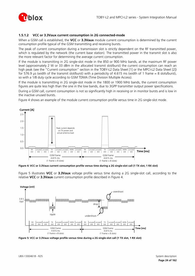
1.5.1.2 VCC or 3.3Vaux current consumption in 2G connected-mode
When a GSM call is established, the VCC or 3.3Vaux module current consumption is determined by the current consumption profile typical of the GSM transmitting and receiving bursts.
The peak of current consumption during a transmission slot is strictly dependent on the RF transmitted power, which is regulated by the network (the current base station). The transmitted power in the transmit slot is also the more relevant factor for determining the average current consumption.
If the module is transmitting in 2G single-slot mode in the 850 or 900 MHz bands, at the maximum RF power level (approximately 2 W or 33 dBm in the allocated transmit slot/burst) the current consumption can reach an high peak (see the “Current consumption” section in the TOBY-L2 Data Sheet [1] or the MPCI-L2 Data Sheet [2]) for 576.9 µs (width of the transmit slot/burst) with a periodicity of 4.615 ms (width of 1 frame = 8 slots/burst), so with a 1/8 duty cycle according to GSM TDMA (Time Division Multiple Access).
If the module is transmitting in 2G single-slot mode in the 1800 or 1900 MHz bands, the current consumption figures are quite less high than the one in the low bands, due to 3GPP transmitter output power specifications.
During a GSM call, current consumption is not so significantly high in receiving or in monitor bursts and is low in the inactive unused bursts.
Figure 4 shows an example of the module current consumption profile versus time in 2G single-slot mode.
Time [ms]RX slot
unused slot
unused slot
TX slot
unused slot
unused slot
MON slot
unused slot
RX slot
unused slot
unused slot
TX slot
unused slot
unused slot
MON slot
unused slot
GSM frame
4.615 ms
(1 frame = 8 slots)
Current [A]
200 mA
60-120 mA
1900 mA
Peak current depends
on TX power and actual antenna load
GSM frame
4.615 ms
(1 frame = 8 slots)
60-120 mA10-40 mA
0.0
1.5
1.0
0.5
2.0
2.5
Figure 4: VCC or 3.3Vaux current consumption profile versus time during a 2G single-slot call (1 TX slot, 1 RX slot)
Figure 5 illustrates VCC or 3.3Vaux voltage profile versus time during a 2G single-slot call, according to the relative VCC or 3.3Vaux current consumption profile described in Figure 4.
Time [ms]
undershoot
overshoot
ripple
drop
Voltage [mV]
3.8 V (typ)
RX slot
unused slot
unused slot
TX slot
unused slot
unused slot
MON slot
unused slot
RX slot
unused slot
unused slot
TX slot
unused slot
unused slot
MON slot
unused slot
GSM frame 4.615 ms
(1 frame = 8 slots)
GSM frame 4.615 ms
(1 frame = 8 slots)
Figure 5: VCC or 3.3Vaux voltage profile versus time during a 2G single-slot call (1 TX slot, 1 RX slot)
TOBY-L2 and MPCI-L2 series - System Integration Manual
UBX-13004618 - R25 System description
Page 25 of 162
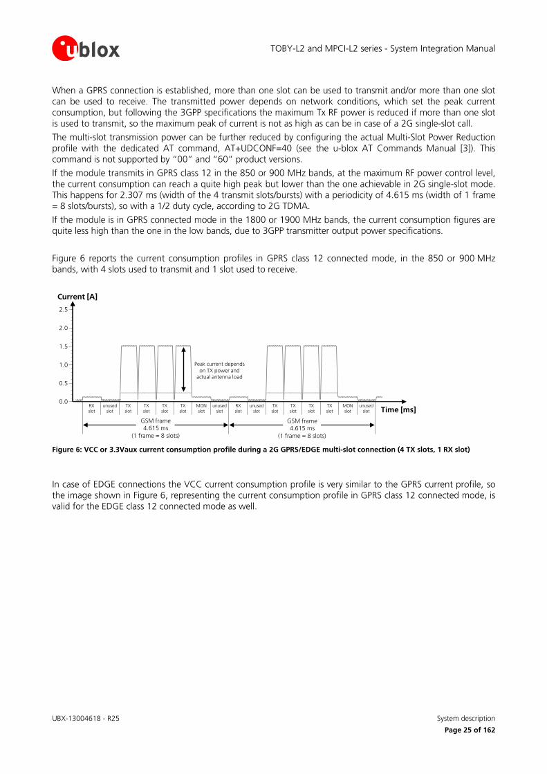
When a GPRS connection is established, more than one slot can be used to transmit and/or more than one slot can be used to receive. The transmitted power depends on network conditions, which set the peak current consumption, but following the 3GPP specifications the maximum Tx RF power is reduced if more than one slot is used to transmit, so the maximum peak of current is not as high as can be in case of a 2G single-slot call.
The multi-slot transmission power can be further reduced by configuring the actual Multi-Slot Power Reduction profile with the dedicated AT command, AT+UDCONF=40 (see the u-blox AT Commands Manual [3]). This command is not supported by “00” and “60” product versions.
If the module transmits in GPRS class 12 in the 850 or 900 MHz bands, at the maximum RF power control level, the current consumption can reach a quite high peak but lower than the one achievable in 2G single-slot mode. This happens for 2.307 ms (width of the 4 transmit slots/bursts) with a periodicity of 4.615 ms (width of 1 frame = 8 slots/bursts), so with a 1/2 duty cycle, according to 2G TDMA.
If the module is in GPRS connected mode in the 1800 or 1900 MHz bands, the current consumption figures are quite less high than the one in the low bands, due to 3GPP transmitter output power specifications.
Figure 6 reports the current consumption profiles in GPRS class 12 connected mode, in the 850 or 900 MHz bands, with 4 slots used to transmit and 1 slot used to receive.
Time [ms]RX slot
unused slot
TX slot
TX slot
TX slot
TX slot
MON slot
unused slot
RX slot
unused slot
TX slot
TX slot
TX slot
TX slot
MON slot
unused slot
GSM frame 4.615 ms
(1 frame = 8 slots)
Current [A]
200mA60-130mA
Peak current depends
on TX power and actual antenna load
GSM frame 4.615 ms
(1 frame = 8 slots)
1600 mA
0.0
1.5
1.0
0.5
2.0
2.5
Figure 6: VCC or 3.3Vaux current consumption profile during a 2G GPRS/EDGE multi-slot connection (4 TX slots, 1 RX slot)
In case of EDGE connections the VCC current consumption profile is very similar to the GPRS current profile, so the image shown in Figure 6, representing the current consumption profile in GPRS class 12 connected mode, is valid for the EDGE class 12 connected mode as well.
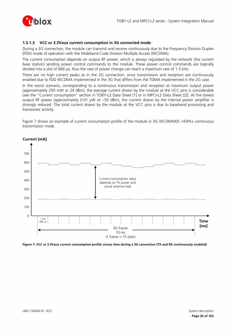
TOBY-L2 and MPCI-L2 series - System Integration Manual
UBX-13004618 - R25 System description
Page 26 of 162
1.5.1.3 VCC or 3.3Vaux current consumption in 3G connected mode
During a 3G connection, the module can transmit and receive continuously due to the Frequency Division Duplex (FDD) mode of operation with the Wideband Code Division Multiple Access (WCDMA).
The current consumption depends on output RF power, which is always regulated by the network (the current base station) sending power control commands to the module. These power control commands are logically divided into a slot of 666 µs, thus the rate of power change can reach a maximum rate of 1.5 kHz.
There are no high current peaks as in the 2G connection, since transmission and reception are continuously enabled due to FDD WCDMA implemented in the 3G that differs from the TDMA implemented in the 2G case.
In the worst scenario, corresponding to a continuous transmission and reception at maximum output power (approximately 250 mW or 24 dBm), the average current drawn by the module at the VCC pins is considerable (see the “Current consumption” section in TOBY-L2 Data Sheet [1] or in MPCI-L2 Data Sheet [2]). At the lowest output RF power (approximately 0.01 µW or –50 dBm), the current drawn by the internal power amplifier is strongly reduced. The total current drawn by the module at the VCC pins is due to baseband processing and transceiver activity.
Figure 7 shows an example of current consumption profile of the module in 3G WCDMA/DC-HSPA+ continuous transmission mode.
Time
[ms]3G frame
10 ms
(1 frame = 15 slots)
Current [mA]
Current consumption value
depends on TX power and
actual antenna load
170 mA
1 slot
666 µs
850 mA
0
300
200
100
500
400
600
700
Figure 7: VCC or 3.3Vaux current consumption profile versus time during a 3G connection (TX and RX continuously enabled)
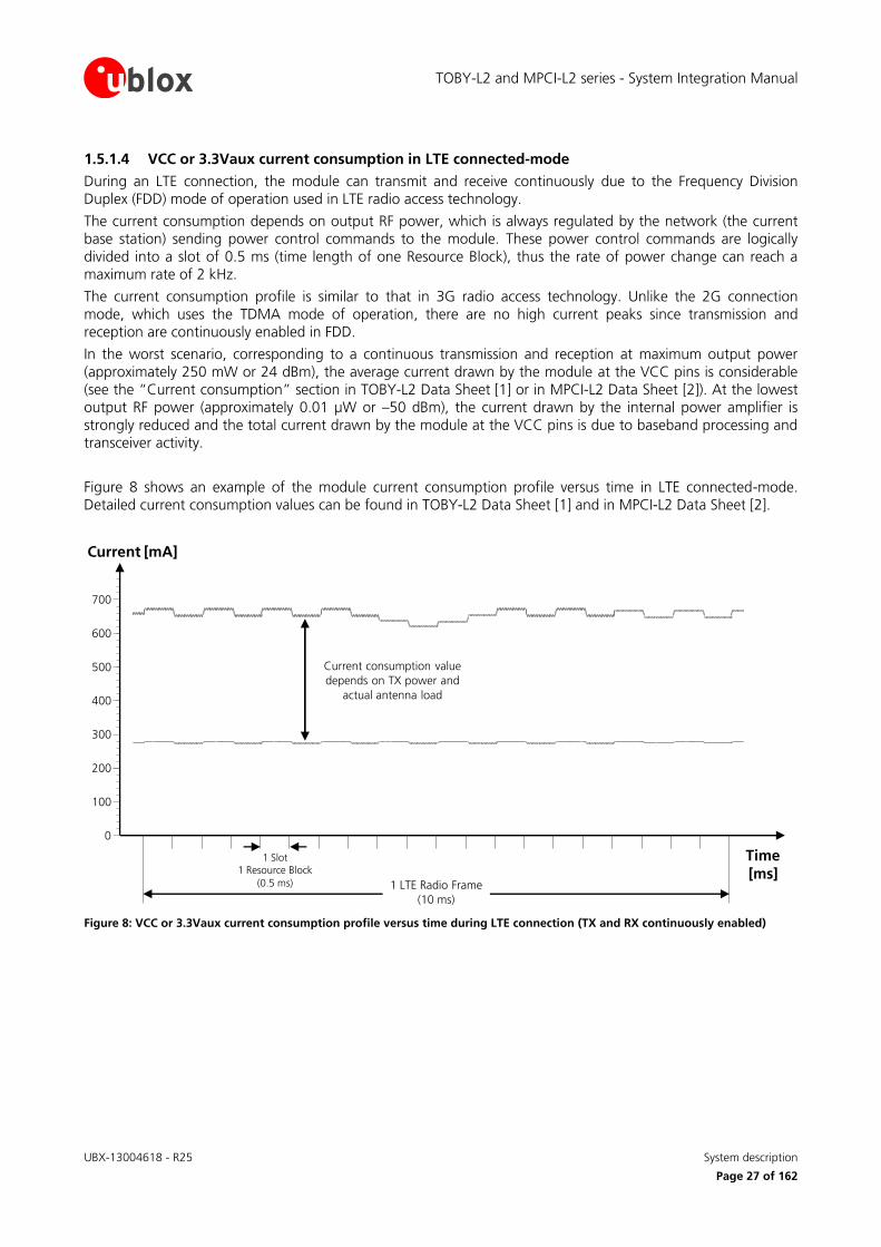
TOBY-L2 and MPCI-L2 series - System Integration Manual
UBX-13004618 - R25 System description
Page 27 of 162
1.5.1.4 VCC or 3.3Vaux current consumption in LTE connected-mode
During an LTE connection, the module can transmit and receive continuously due to the Frequency Division Duplex (FDD) mode of operation used in LTE radio access technology.
The current consumption depends on output RF power, which is always regulated by the network (the current base station) sending power control commands to the module. These power control commands are logically divided into a slot of 0.5 ms (time length of one Resource Block), thus the rate of power change can reach a maximum rate of 2 kHz.
The current consumption profile is similar to that in 3G radio access technology. Unlike the 2G connection mode, which uses the TDMA mode of operation, there are no high current peaks since transmission and reception are continuously enabled in FDD.
In the worst scenario, corresponding to a continuous transmission and reception at maximum output power (approximately 250 mW or 24 dBm), the average current drawn by the module at the VCC pins is considerable (see the “Current consumption” section in TOBY-L2 Data Sheet [1] or in MPCI-L2 Data Sheet [2]). At the lowest output RF power (approximately 0.01 µW or –50 dBm), the current drawn by the internal power amplifier is strongly reduced and the total current drawn by the module at the VCC pins is due to baseband processing and transceiver activity.
Figure 8 shows an example of the module current consumption profile versus time in LTE connected-mode. Detailed current consumption values can be found in TOBY-L2 Data Sheet [1] and in MPCI-L2 Data Sheet [2].
Time [ms]
Current [mA]
Current consumption value
depends on TX power and
actual antenna load
1 Slot1 Resource Block
(0.5 ms) 1 LTE Radio Frame
(10 ms)
0
300
200
100
500
400
600
700
Figure 8: VCC or 3.3Vaux current consumption profile versus time during LTE connection (TX and RX continuously enabled)
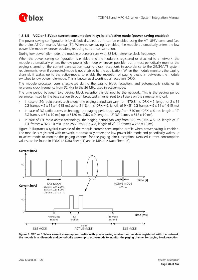
TOBY-L2 and MPCI-L2 series - System Integration Manual
UBX-13004618 - R25 System description
Page 28 of 162
1.5.1.5 VCC or 3.3Vaux current consumption in cyclic idle/active mode (power saving enabled)
The power saving configuration is by default disabled, but it can be enabled using the AT+UPSV command (see the u-blox AT Commands Manual [3]). When power saving is enabled, the module automatically enters the low power idle-mode whenever possible, reducing current consumption.
During low power idle-mode, the module processor runs with 32 kHz reference clock frequency.
When the power saving configuration is enabled and the module is registered or attached to a network, the module automatically enters the low power idle-mode whenever possible, but it must periodically monitor the paging channel of the current base station (paging block reception), in accordance to the 2G/3G/LTE system requirements, even if connected-mode is not enabled by the application. When the module monitors the paging channel, it wakes up to the active-mode, to enable the reception of paging block. In between, the module switches to low power idle-mode. This is known as discontinuous reception (DRX).
The module processor core is activated during the paging block reception, and automatically switches its reference clock frequency from 32 kHz to the 26 MHz used in active-mode.
The time period between two paging block receptions is defined by the network. This is the paging period parameter, fixed by the base station through broadcast channel sent to all users on the same serving cell:
In case of 2G radio access technology, the paging period can vary from 470.8 ms (DRX = 2, length of 2 x 51 2G frames = 2 x 51 x 4.615 ms) up to 2118.4 ms (DRX = 9, length of 9 x 51 2G frames = 9 x 51 x 4.615 ms)
In case of 3G radio access technology, the paging period can vary from 640 ms (DRX = 6, i.e. length of 26
3G frames = 64 x 10 ms) up to 5120 ms (DRX = 9, length of 29 3G frames = 512 x 10 ms).
In case of LTE radio access technology, the paging period can vary from 320 ms (DRX = 5, i.e. length of 25
LTE frames = 32 x 10 ms) up to 2560 ms (DRX = 8, length of 28 LTE frames = 256 x 10 ms).
Figure 9 illustrates a typical example of the module current consumption profile when power saving is enabled. The module is registered with network, automatically enters the low power idle-mode and periodically wakes up to active-mode to monitor the paging channel for the paging block reception. Detailed current consumption values can be found in TOBY-L2 Data Sheet [1] and in MPCI-L2 Data Sheet [2].
~50 ms
IDLE MODE ACTIVE MODE IDLE MODE
Active Mode
EnabledIdle Mode
Enabled
2G case: 0.44-2.09 s 3G case: 0.61-5.09 s LTE case: 0.27-2.51 s
IDLE MODE~50 ms
ACTIVE MODE
Time [s]
Current [mA]
Time [ms]
Current [mA]
RX
Enabled
0
100
0
100
Figure 9: VCC or 3.3Vaux current consumption profile with power saving enabled and module registered with the network: the module is in idle-mode and periodically wakes up to active-mode to monitor the paging channel for paging block reception
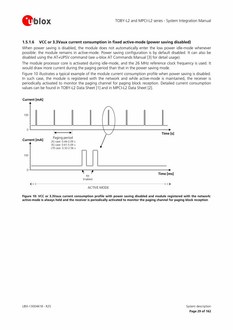
TOBY-L2 and MPCI-L2 series - System Integration Manual
UBX-13004618 - R25 System description
Page 29 of 162
1.5.1.6 VCC or 3.3Vaux current consumption in fixed active-mode (power saving disabled)
When power saving is disabled, the module does not automatically enter the low power idle-mode whenever possible: the module remains in active-mode. Power saving configuration is by default disabled. It can also be disabled using the AT+UPSV command (see u-blox AT Commands Manual [3] for detail usage).
The module processor core is activated during idle-mode, and the 26 MHz reference clock frequency is used. It would draw more current during the paging period than that in the power saving mode.
Figure 10 illustrates a typical example of the module current consumption profile when power saving is disabled. In such case, the module is registered with the network and while active-mode is maintained, the receiver is periodically activated to monitor the paging channel for paging block reception. Detailed current consumption values can be found in TOBY-L2 Data Sheet [1] and in MPCI-L2 Data Sheet [2].
ACTIVE MODE
2G case: 0.44-2.09 s
3G case: 0.61-5.09 s
LTE case: 0.32-2.56 s
Paging period
Time [s]
Current [mA]
Time [ms]
Current [mA]
RX
Enabled
0
100
0
100
Figure 10: VCC or 3.3Vaux current consumption profile with power saving disabled and module registered with the network: active-mode is always held and the receiver is periodically activated to monitor the paging channel for paging block reception
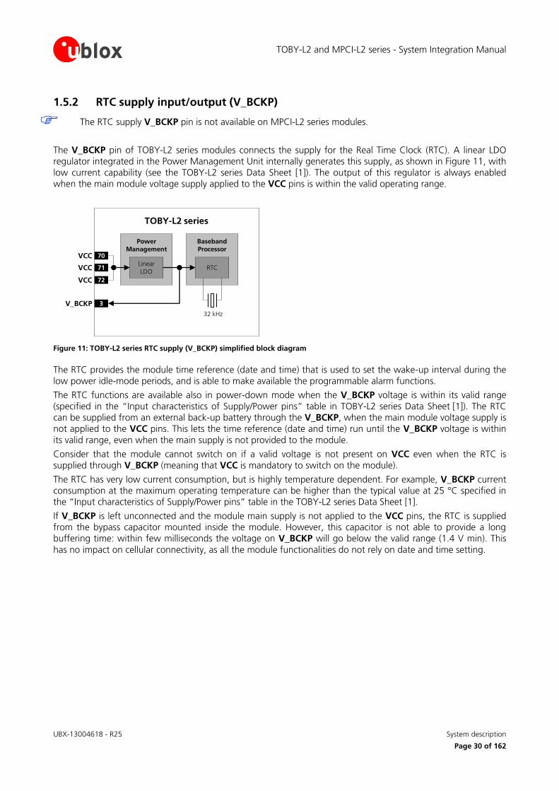
TOBY-L2 and MPCI-L2 series - System Integration Manual
UBX-13004618 - R25 System description
Page 30 of 162
1.5.2 RTC supply input/output (V_BCKP)
The RTC supply V_BCKP pin is not available on MPCI-L2 series modules.
The V_BCKP pin of TOBY-L2 series modules connects the supply for the Real Time Clock (RTC). A linear LDO regulator integrated in the Power Management Unit internally generates this supply, as shown in Figure 11, with low current capability (see the TOBY-L2 series Data Sheet [1]). The output of this regulator is always enabled when the main module voltage supply applied to the VCC pins is within the valid operating range.
Baseband
Processor70VCC
71VCC
72VCC
3V_BCKP
Linear
LDO
Power
Management
TOBY-L2 series
32 kHz
RTC
Figure 11: TOBY-L2 series RTC supply (V_BCKP) simplified block diagram
The RTC provides the module time reference (date and time) that is used to set the wake-up interval during the low power idle-mode periods, and is able to make available the programmable alarm functions.
The RTC functions are available also in power-down mode when the V_BCKP voltage is within its valid range (specified in the “Input characteristics of Supply/Power pins” table in TOBY-L2 series Data Sheet [1]). The RTC can be supplied from an external back-up battery through the V_BCKP, when the main module voltage supply is not applied to the VCC pins. This lets the time reference (date and time) run until the V_BCKP voltage is within its valid range, even when the main supply is not provided to the module.
Consider that the module cannot switch on if a valid voltage is not present on VCC even when the RTC is supplied through V_BCKP (meaning that VCC is mandatory to switch on the module).
The RTC has very low current consumption, but is highly temperature dependent. For example, V_BCKP current consumption at the maximum operating temperature can be higher than the typical value at 25 °C specified in the “Input characteristics of Supply/Power pins” table in the TOBY-L2 series Data Sheet [1].
If V_BCKP is left unconnected and the module main supply is not applied to the VCC pins, the RTC is supplied from the bypass capacitor mounted inside the module. However, this capacitor is not able to provide a long buffering time: within few milliseconds the voltage on V_BCKP will go below the valid range (1.4 V min). This has no impact on cellular connectivity, as all the module functionalities do not rely on date and time setting.
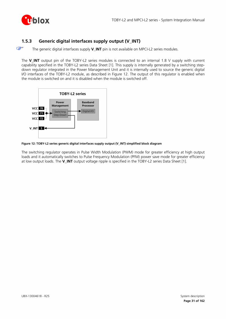
TOBY-L2 and MPCI-L2 series - System Integration Manual
UBX-13004618 - R25 System description
Page 31 of 162
1.5.3 Generic digital interfaces supply output (V_INT)
The generic digital interfaces supply V_INT pin is not available on MPCI-L2 series modules.
The V_INT output pin of the TOBY-L2 series modules is connected to an internal 1.8 V supply with current capability specified in the TOBY-L2 series Data Sheet [1]. This supply is internally generated by a switching step-down regulator integrated in the Power Management Unit and it is internally used to source the generic digital I/O interfaces of the TOBY-L2 module, as described in Figure 12. The output of this regulator is enabled when the module is switched on and it is disabled when the module is switched off.
Baseband
Processor70VCC
71VCC
72VCC
5V_INT
SwitchingStep-Down
Power
Management
TOBY-L2 series
Digital I/O
Figure 12: TOBY-L2 series generic digital interfaces supply output (V_INT) simplified block diagram
The switching regulator operates in Pulse Width Modulation (PWM) mode for greater efficiency at high output loads and it automatically switches to Pulse Frequency Modulation (PFM) power save mode for greater efficiency at low output loads. The V_INT output voltage ripple is specified in the TOBY-L2 series Data Sheet [1].
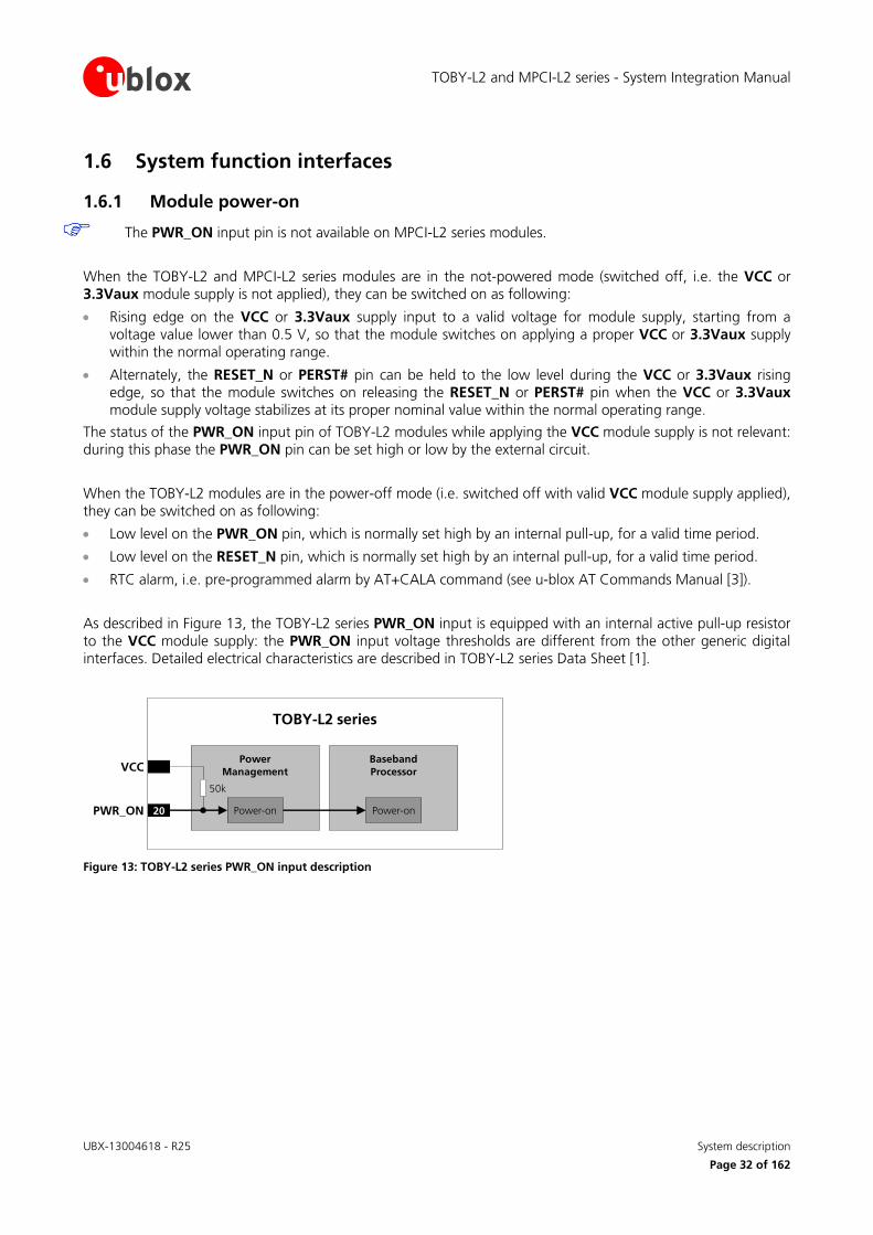
TOBY-L2 and MPCI-L2 series - System Integration Manual
UBX-13004618 - R25 System description
Page 32 of 162
1.6 System function interfaces
1.6.1 Module power-on
The PWR_ON input pin is not available on MPCI-L2 series modules.
When the TOBY-L2 and MPCI-L2 series modules are in the not-powered mode (switched off, i.e. the VCC or 3.3Vaux module supply is not applied), they can be switched on as following:
Rising edge on the VCC or 3.3Vaux supply input to a valid voltage for module supply, starting from a voltage value lower than 0.5 V, so that the module switches on applying a proper VCC or 3.3Vaux supply within the normal operating range.
Alternately, the RESET_N or PERST# pin can be held to the low level during the VCC or 3.3Vaux rising edge, so that the module switches on releasing the RESET_N or PERST# pin when the VCC or 3.3Vaux module supply voltage stabilizes at its proper nominal value within the normal operating range.
The status of the PWR_ON input pin of TOBY-L2 modules while applying the VCC module supply is not relevant: during this phase the PWR_ON pin can be set high or low by the external circuit.
When the TOBY-L2 modules are in the power-off mode (i.e. switched off with valid VCC module supply applied), they can be switched on as following:
Low level on the PWR_ON pin, which is normally set high by an internal pull-up, for a valid time period.
Low level on the RESET_N pin, which is normally set high by an internal pull-up, for a valid time period.
RTC alarm, i.e. pre-programmed alarm by AT+CALA command (see u-blox AT Commands Manual [3]).
As described in Figure 13, the TOBY-L2 series PWR_ON input is equipped with an internal active pull-up resistor to the VCC module supply: the PWR_ON input voltage thresholds are different from the other generic digital interfaces. Detailed electrical characteristics are described in TOBY-L2 series Data Sheet [1].
Baseband
Processor
20PWR_ON
TOBY-L2 series
VCC
Power-on
Power
Management
Power-on
50k
Figure 13: TOBY-L2 series PWR_ON input description
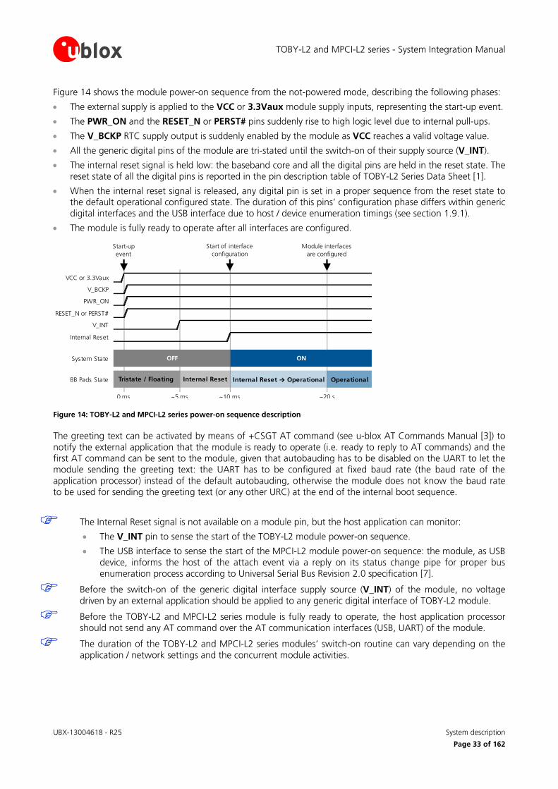
TOBY-L2 and MPCI-L2 series - System Integration Manual
UBX-13004618 - R25 System description
Page 33 of 162
Figure 14 shows the module power-on sequence from the not-powered mode, describing the following phases:
The external supply is applied to the VCC or 3.3Vaux module supply inputs, representing the start-up event.
The PWR_ON and the RESET_N or PERST# pins suddenly rise to high logic level due to internal pull-ups.
The V_BCKP RTC supply output is suddenly enabled by the module as VCC reaches a valid voltage value.
All the generic digital pins of the module are tri-stated until the switch-on of their supply source (V_INT).
The internal reset signal is held low: the baseband core and all the digital pins are held in the reset state. The reset state of all the digital pins is reported in the pin description table of TOBY-L2 Series Data Sheet [1].
When the internal reset signal is released, any digital pin is set in a proper sequence from the reset state to the default operational configured state. The duration of this pins’ configuration phase differs within generic digital interfaces and the USB interface due to host / device enumeration timings (see section 1.9.1).
The module is fully ready to operate after all interfaces are configured.
VCC or 3.3Vaux
V_BCKP
PWR_ON
RESET_N or PERST#
V_INT
Internal Reset
System State
BB Pads State Internal Reset → Operational OperationalTristate / Floating Internal Reset
OFF ON
0 ms ~10 ms ~20 s
Start of interface
configuration
Module interfaces
are configured
Start-up
event
~5 ms
Figure 14: TOBY-L2 and MPCI-L2 series power-on sequence description
The greeting text can be activated by means of +CSGT AT command (see u-blox AT Commands Manual [3]) to notify the external application that the module is ready to operate (i.e. ready to reply to AT commands) and the first AT command can be sent to the module, given that autobauding has to be disabled on the UART to let the module sending the greeting text: the UART has to be configured at fixed baud rate (the baud rate of the application processor) instead of the default autobauding, otherwise the module does not know the baud rate to be used for sending the greeting text (or any other URC) at the end of the internal boot sequence.
The Internal Reset signal is not available on a module pin, but the host application can monitor:
The V_INT pin to sense the start of the TOBY-L2 module power-on sequence.
The USB interface to sense the start of the MPCI-L2 module power-on sequence: the module, as USB device, informs the host of the attach event via a reply on its status change pipe for proper bus enumeration process according to Universal Serial Bus Revision 2.0 specification [7].
Before the switch-on of the generic digital interface supply source (V_INT) of the module, no voltage driven by an external application should be applied to any generic digital interface of TOBY-L2 module.
Before the TOBY-L2 and MPCI-L2 series module is fully ready to operate, the host application processor should not send any AT command over the AT communication interfaces (USB, UART) of the module.
The duration of the TOBY-L2 and MPCI-L2 series modules’ switch-on routine can vary depending on the application / network settings and the concurrent module activities.
TOBY-L2 and MPCI-L2 series - System Integration Manual
UBX-13004618 - R25 System description
Page 34 of 162
1.6.2 Module power-off
TOBY-L2 series can be properly switched off by:
AT+CPWROFF command (see u-blox AT Commands Manual [3]). The current parameter settings are saved in the module’s non-volatile memory and a proper network detach is performed.
The MPCI-L2 series modules do not switch off by the AT+CPWROFF command as the TOBY-L2 modules, but the AT+CPWROFF command causes a reset (reboot) of the module due to the MPCI-L2 module’s internal configuration: the command stores the actual parameter settings in the non-volatile memory of MPCI-L2 modules and performs a network detach, with a subsequent reset (reboot) of the module.
An abrupt under-voltage shutdown occurs on TOBY-L2 and MPCI-L2 series modules when the VCC or 3.3Vaux module supply is removed. If this occurs, it is not possible to perform the storing of the current parameter settings in the module’s non-volatile memory or to perform the proper network detach.
It is highly recommended to avoid an abrupt removal of the VCC supply during TOBY-L2 modules normal operations: the power off procedure must be started by the AT+CPWROFF command, waiting the command response for a proper time period (see u-blox AT Commands Manual [3]), and then a proper VCC supply has to be held at least until the end of the modules’ internal power off sequence, which occurs when the generic digital interfaces supply output (V_INT) is switched off by the module.
It is highly recommended to avoid an abrupt removal of the 3.3Vaux supply during MPCI-L2 modules normal operations: the power off procedure must be started by setting the MPCI-L2 module in the halt mode by the AT+CFUN=127 command (which stores the actual parameter settings in the non-volatile memory of the module and performs a network detach), waiting the command response for a proper time period (see the u-blox AT Commands Manual [3]), and then the 3.3Vaux supply can be removed.
An abrupt hardware shutdown occurs on TOBY-L2 series modules when a low level is applied on the RESET_N pin for a specific time period. In this case, the current parameter settings are not saved in the module’s non-volatile memory and a proper network detach is not performed.
It is highly recommended to avoid an abrupt hardware shutdown of the module by forcing a low level on the RESET_N input pin during module normal operation: the RESET_N line should be set low only if reset or shutdown via AT commands fails or if the module does not reply to a specific AT command after a time period longer than the one defined in the u-blox AT Commands Manual [3].
An over-temperature or an under-temperature shutdown occurs on TOBY-L2 and MPCI-L2 series modules when the temperature measured within the cellular module reaches the dangerous area, if the optional Smart Temperature Supervisor feature is enabled and configured by the dedicated AT command. For more details see u-blox AT Commands Manual [3], +USTS AT command.
The Smart Temperature Supervisor feature is not supported by the “00”, “01”, “60” product versions.
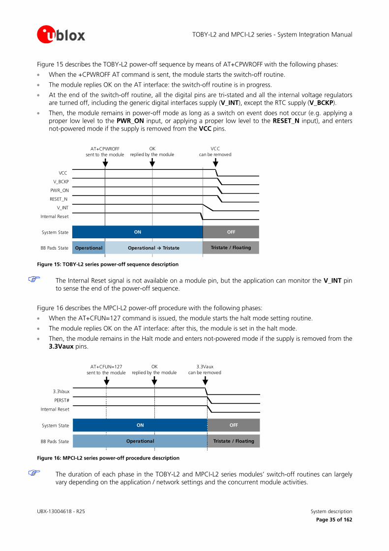
TOBY-L2 and MPCI-L2 series - System Integration Manual
UBX-13004618 - R25 System description
Page 35 of 162
Figure 15 describes the TOBY-L2 power-off sequence by means of AT+CPWROFF with the following phases:
When the +CPWROFF AT command is sent, the module starts the switch-off routine.
The module replies OK on the AT interface: the switch-off routine is in progress.
At the end of the switch-off routine, all the digital pins are tri-stated and all the internal voltage regulators are turned off, including the generic digital interfaces supply (V_INT), except the RTC supply (V_BCKP).
Then, the module remains in power-off mode as long as a switch on event does not occur (e.g. applying a proper low level to the PWR_ON input, or applying a proper low level to the RESET_N input), and enters not-powered mode if the supply is removed from the VCC pins.
VCC
V_BCKP
PWR_ON
RESET_N
V_INT
Internal Reset
System State
BB Pads State Operational
OFF
Tristate / Floating
ON
Operational → Tristate
AT+CPWROFF
sent to the module
0 s ~2.5 s ~5 s
OK
replied by the module
VCC
can be removed
Figure 15: TOBY-L2 series power-off sequence description
The Internal Reset signal is not available on a module pin, but the application can monitor the V_INT pin to sense the end of the power-off sequence.
Figure 16 describes the MPCI-L2 power-off procedure with the following phases:
When the AT+CFUN=127 command is issued, the module starts the halt mode setting routine.
The module replies OK on the AT interface: after this, the module is set in the halt mode.
Then, the module remains in the Halt mode and enters not-powered mode if the supply is removed from the 3.3Vaux pins.
3.3Vaux
PERST#
Internal Reset
System State
BB Pads State
OFFON
Tristate / FloatingOperational
AT+CFUN=127
sent to the module
0 s ~2.5 s ~5 s
OK
replied by the module
3.3Vaux
can be removed
Figure 16: MPCI-L2 series power-off procedure description
The duration of each phase in the TOBY-L2 and MPCI-L2 series modules’ switch-off routines can largely vary depending on the application / network settings and the concurrent module activities.
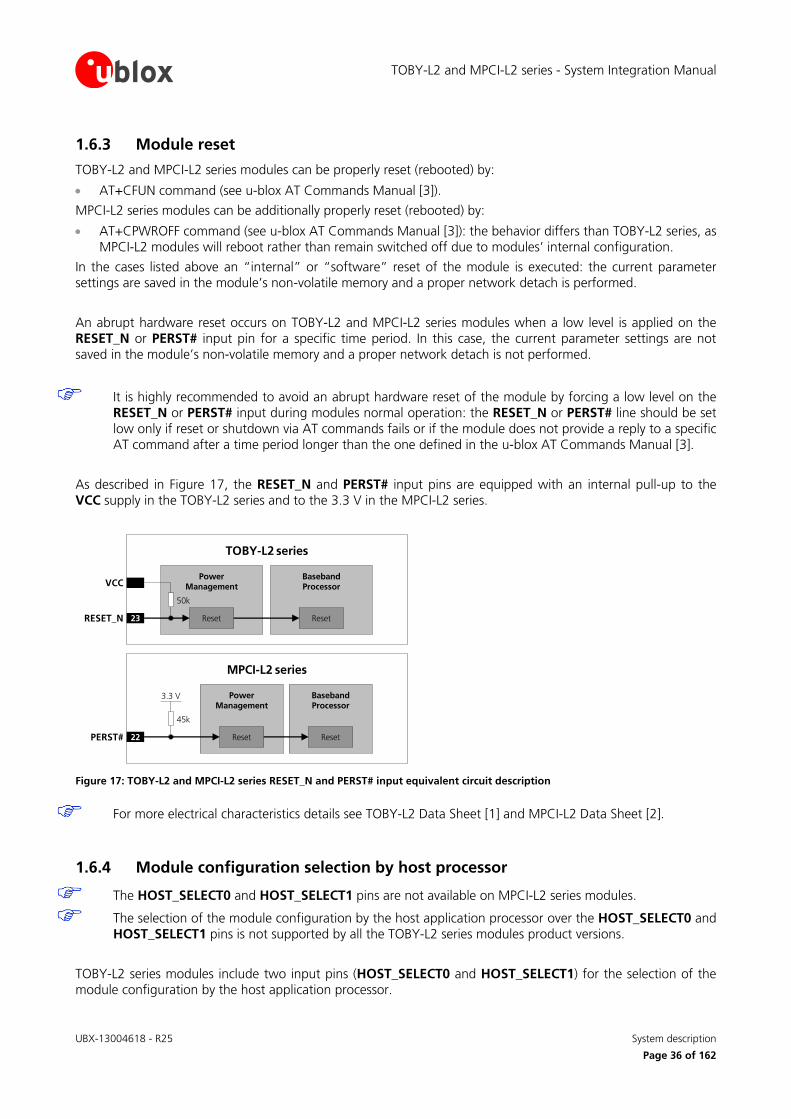
TOBY-L2 and MPCI-L2 series - System Integration Manual
UBX-13004618 - R25 System description
Page 36 of 162
1.6.3 Module reset
TOBY-L2 and MPCI-L2 series modules can be properly reset (rebooted) by:
AT+CFUN command (see u-blox AT Commands Manual [3]).
MPCI-L2 series modules can be additionally properly reset (rebooted) by:
AT+CPWROFF command (see u-blox AT Commands Manual [3]): the behavior differs than TOBY-L2 series, as MPCI-L2 modules will reboot rather than remain switched off due to modules’ internal configuration.
In the cases listed above an “internal” or “software” reset of the module is executed: the current parameter settings are saved in the module’s non-volatile memory and a proper network detach is performed.
An abrupt hardware reset occurs on TOBY-L2 and MPCI-L2 series modules when a low level is applied on the RESET_N or PERST# input pin for a specific time period. In this case, the current parameter settings are not saved in the module’s non-volatile memory and a proper network detach is not performed.
It is highly recommended to avoid an abrupt hardware reset of the module by forcing a low level on the RESET_N or PERST# input during modules normal operation: the RESET_N or PERST# line should be set low only if reset or shutdown via AT commands fails or if the module does not provide a reply to a specific AT command after a time period longer than the one defined in the u-blox AT Commands Manual [3].
As described in Figure 17, the RESET_N and PERST# input pins are equipped with an internal pull-up to the VCC supply in the TOBY-L2 series and to the 3.3 V in the MPCI-L2 series.
Baseband Processor
23RESET_N
TOBY-L2 series
VCC
Reset
Power Management
Reset
50k
Baseband Processor
22PERST#
MPCI-L2 series
Reset
Power Management
Reset
45k
3.3 V
Figure 17: TOBY-L2 and MPCI-L2 series RESET_N and PERST# input equivalent circuit description
For more electrical characteristics details see TOBY-L2 Data Sheet [1] and MPCI-L2 Data Sheet [2].
1.6.4 Module configuration selection by host processor
The HOST_SELECT0 and HOST_SELECT1 pins are not available on MPCI-L2 series modules.
The selection of the module configuration by the host application processor over the HOST_SELECT0 and HOST_SELECT1 pins is not supported by all the TOBY-L2 series modules product versions.
TOBY-L2 series modules include two input pins (HOST_SELECT0 and HOST_SELECT1) for the selection of the module configuration by the host application processor.
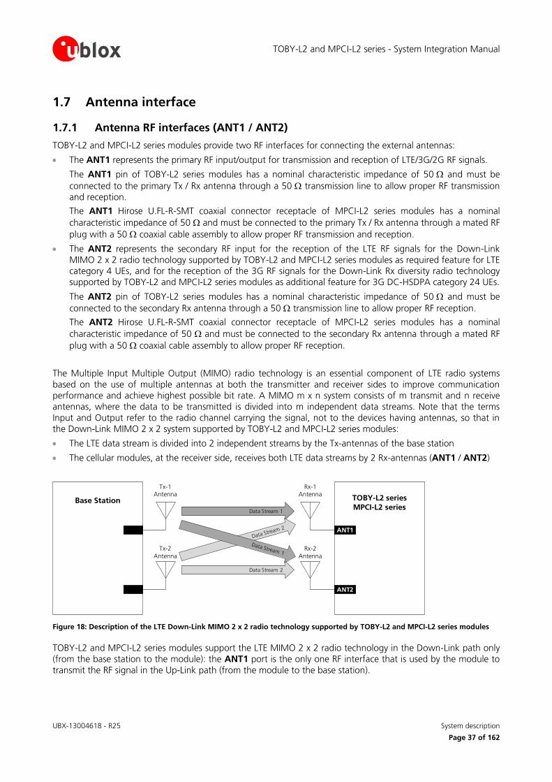
TOBY-L2 and MPCI-L2 series - System Integration Manual
UBX-13004618 - R25 System description
Page 37 of 162
1.7 Antenna interface
1.7.1 Antenna RF interfaces (ANT1 / ANT2)
TOBY-L2 and MPCI-L2 series modules provide two RF interfaces for connecting the external antennas:
The ANT1 represents the primary RF input/output for transmission and reception of LTE/3G/2G RF signals.
The ANT1 pin of TOBY-L2 series modules has a nominal characteristic impedance of 50 and must be
connected to the primary Tx / Rx antenna through a 50 transmission line to allow proper RF transmission and reception.
The ANT1 Hirose U.FL-R-SMT coaxial connector receptacle of MPCI-L2 series modules has a nominal
characteristic impedance of 50 and must be connected to the primary Tx / Rx antenna through a mated RF
plug with a 50 coaxial cable assembly to allow proper RF transmission and reception.
The ANT2 represents the secondary RF input for the reception of the LTE RF signals for the Down-Link MIMO 2 x 2 radio technology supported by TOBY-L2 and MPCI-L2 series modules as required feature for LTE category 4 UEs, and for the reception of the 3G RF signals for the Down-Link Rx diversity radio technology supported by TOBY-L2 and MPCI-L2 series modules as additional feature for 3G DC-HSDPA category 24 UEs.
The ANT2 pin of TOBY-L2 series modules has a nominal characteristic impedance of 50 and must be
connected to the secondary Rx antenna through a 50 transmission line to allow proper RF reception.
The ANT2 Hirose U.FL-R-SMT coaxial connector receptacle of MPCI-L2 series modules has a nominal
characteristic impedance of 50 and must be connected to the secondary Rx antenna through a mated RF
plug with a 50 coaxial cable assembly to allow proper RF reception.
The Multiple Input Multiple Output (MIMO) radio technology is an essential component of LTE radio systems based on the use of multiple antennas at both the transmitter and receiver sides to improve communication performance and achieve highest possible bit rate. A MIMO m x n system consists of m transmit and n receive antennas, where the data to be transmitted is divided into m independent data streams. Note that the terms Input and Output refer to the radio channel carrying the signal, not to the devices having antennas, so that in the Down-Link MIMO 2 x 2 system supported by TOBY-L2 and MPCI-L2 series modules:
The LTE data stream is divided into 2 independent streams by the Tx-antennas of the base station
The cellular modules, at the receiver side, receives both LTE data streams by 2 Rx-antennas (ANT1 / ANT2)
Base Station
Tx-1 Antenna
Tx-2 Antenna
TOBY-L2 series
MPCI-L2 series
ANT1
Rx-1 Antenna
ANT2
Rx-2 Antenna
Data Stream 1
Data Stream 2
Figure 18: Description of the LTE Down-Link MIMO 2 x 2 radio technology supported by TOBY-L2 and MPCI-L2 series modules
TOBY-L2 and MPCI-L2 series modules support the LTE MIMO 2 x 2 radio technology in the Down-Link path only (from the base station to the module): the ANT1 port is the only one RF interface that is used by the module to transmit the RF signal in the Up-Link path (from the module to the base station).
TOBY-L2 and MPCI-L2 series - System Integration Manual
UBX-13004618 - R25 System description
Page 38 of 162
1.7.1.1 Antenna RF interfaces requirements
Table 8, Table 9 and Table 10 summarize the requirements for the antennas RF interfaces (ANT1 / ANT2). See section 2.4.1 for suggestions to properly design antennas circuits compliant with these requirements.
The antenna circuits affect the RF compliance of the device integrating TOBY-L2 and MPCI-L2 series modules with applicable required certification schemes (for more details see section 4). Compliance is guaranteed if the antenna RF interfaces (ANT1 / ANT2) requirements summarized in Table 8, Table 9 and Table 10 are fulfilled.
Item Requirements Remarks
Impedance 50 nominal characteristic impedance The impedance of the antenna RF connection must
match the 50 impedance of the ANT1 port.
Frequency Range See the TOBY-L2 series Data Sheet [1] and the MPCI-L2 series Data Sheet [2]
The required frequency range of the antenna connected to ANT1 port depends on the operating bands of the
used cellular module and the used mobile network.
Return Loss S11
< -10 dB (VSWR < 2:1) recommended
S11
< -6 dB (VSWR < 3:1) acceptable
The Return loss or the S11
, as the VSWR, refers to the
amount of reflected power, measuring how well the
primary antenna RF connection matches the 50 characteristic impedance of the ANT1 port.
The impedance of the antenna termination must match
as much as possible the 50 nominal impedance of the ANT1 port over the operating frequency range, reducing
as much as possible the amount of reflected power.
Efficiency > -1.5 dB ( > 70% ) recommended
> -3.0 dB ( > 50% ) acceptable
The radiation efficiency is the ratio of the radiated power to the power delivered to antenna input: the efficiency is
a measure of how well an antenna receives or transmits.
The radiation efficiency of the antenna connected to the
ANT1 port needs to be enough high over the operating frequency range to comply with the Over-The-Air (OTA) radiated performance requirements, as Total Radiated
Power (TRP) and the Total Isotropic Sensitivity (TIS), specified by applicable related certification schemes.
Maximum Gain According to radiation exposure limits The power gain of an antenna is the radiation efficiency multiplied by the directivity: the gain describes how much power is transmitted in the direction of peak
radiation to that of an isotropic source.
The maximum gain of the antenna connected to ANT1
port must not exceed the herein stated value to comply with regulatory agencies radiation exposure limits.
For additional info see sections 4.2.2 and/or 4.3.1
Input Power > 33 dBm ( > 2 W ) The antenna connected to the ANT1 port must support with adequate margin the maximum power transmitted by the modules.
Table 8: Summary of primary Tx/Rx antenna RF interface (ANT1) requirements
TOBY-L2 and MPCI-L2 series - System Integration Manual
UBX-13004618 - R25 System description
Page 39 of 162
Item Requirements Remarks
Impedance 50 nominal characteristic impedance The impedance of the antenna RF connection must
match the 50 impedance of the ANT2 port.
Frequency Range See the TOBY-L2 series Data Sheet [1] and the MPCI-L2 series Data Sheet [2]
The required frequency range of the antennas connected to ANT2 port depends on the operating bands of the
used cellular module and the used Mobile Network.
Return Loss S11
< -10 dB (VSWR < 2:1) recommended
S11
< -6 dB (VSWR < 3:1) acceptable
The Return loss or the S11
, as the VSWR, refers to the amount of reflected power, measuring how well the
secondary antenna RF connection matches the 50 characteristic impedance of the ANT2 port.
The impedance of the antenna termination must match
as much as possible the 50 nominal impedance of the ANT2 port over the operating frequency range, reducing
as much as possible the amount of reflected power.
Efficiency > -1.5 dB ( > 70% ) recommended
> -3.0 dB ( > 50% ) acceptable
The radiation efficiency is the ratio of the radiated power to the power delivered to antenna input: the efficiency is
a measure of how well an antenna receives or transmits.
The radiation efficiency of the antenna connected to the ANT2 port needs to be enough high over the operating
frequency range to comply with the Over-The-Air (OTA) radiated performance requirements, as the TIS, specified
by applicable related certification schemes.
Table 9: Summary of secondary Rx antenna RF interface (ANT2) requirements
Item Requirements Remarks
Efficiency imbalance < 0.5 dB recommended
< 1.0 dB acceptable
The radiation efficiency imbalance is the ratio of the primary (ANT1) antenna efficiency to the secondary (ANT2) antenna efficiency: the efficiency imbalance is a
measure of how much better an antenna receives or transmits compared to the other antenna.
The radiation efficiency of the secondary antenna needs
to be roughly the same of the radiation efficiency of the primary antenna for good RF performance.
Envelope Correlation Coefficient
< 0.4 recommended
< 0.5 acceptable
The Envelope Correlation Coefficient (ECC) between the primary (ANT1) and the secondary (ANT2) antenna is an indicator of 3D radiation pattern similarity between the
two antennas: low ECC results from antenna patterns with radiation lobes in different directions.
The ECC between primary and secondary antenna needs
to be enough low to comply with radiated performance requirements specified by related certification schemes.
Isolation > 15 dB recommended
> 10 dB acceptable
The antenna to antenna isolation is the loss between the primary (ANT1) and the secondary (ANT2) antenna: high isolation results from low coupled antennas.
The isolation between primary and secondary antenna
needs to be high for good RF performance.
Table 10: Summary of primary (ANT1) and secondary (ANT2) antennas relationship requirements
TOBY-L2 and MPCI-L2 series - System Integration Manual
UBX-13004618 - R25 System description
Page 40 of 162
1.7.2 Antenna detection interface (ANT_DET)
Antenna detection (ANT_DET) is not available on MPCI-L2 series modules.
Antenna detection (ANT_DET) is not supported by TOBY-L2 “00”, “01” and “60” product versions.
The antenna detection is based on ADC measurement. The ANT_DET pin is an Analog to Digital Converter (ADC) provided to sense the antenna presence.
The antenna detection function provided by ANT_DET pin is an optional feature that can be implemented if the application requires it. The antenna detection is forced by the +UANTR AT command. See the u-blox AT Commands Manual [3] for more details on this feature.
The ANT_DET pin generates a DC current (for detailed characteristics see the TOBY-L2 series Data Sheet [1]) and measures the resulting DC voltage, thus determining the resistance from the antenna connector provided on the application board to GND. So, the requirements to achieve antenna detection functionality are the following:
an RF antenna assembly with a built-in resistor (diagnostic circuit) must be used
an antenna detection circuit must be implemented on the application board
See section 2.4.2 for antenna detection circuit on application board and diagnostic circuit on antenna assembly design-in guidelines.
1.8 SIM interface
1.8.1 SIM interface
TOBY-L2 and MPCI-L2 series modules provide high-speed SIM/ME interface including automatic detection and configuration of the voltage required by the connected SIM card or chip.
Both 1.8 V and 3 V SIM types are supported. Activation and deactivation with automatic voltage switch from 1.8 V to 3 V are implemented, according to ISO-IEC 7816-3 specifications. The VSIM or UIM_PWR supply output provides internal short circuit protection to limit start-up current and protect the SIM to short circuits.
The SIM driver supports the PPS (Protocol and Parameter Selection) procedure for baud-rate selection, according to the values determined by the SIM card or chip.
1.8.2 SIM detection interface
SIM detection (GPIO5) is not available on MPCI-L2 series modules.
SIM detection (GPIO5) is not supported by TOBY-L2 “00”, “01” and “60” product versions.
The GPIO5 pin is by default configured to detect the external SIM card mechanical / physical presence. The pin is configured as input, and it can sense SIM card presence as intended to be properly connected to the mechanical switch of a SIM card holder as described in section 2.5:
Low logic level at GPIO5 input pin is recognized as SIM card not present
High logic level at GPIO5 input pin is recognized as SIM card present
The SIM card detection function provided by GPIO5 pin is an optional feature that can be implemented / used or not according to the application requirements: an Unsolicited Result Code (URC) is generated each time that there is a change of status (for more details see u-blox AT Commands Manual [3], +UGPIOC, +CIND, +CMER).
The optional function “SIM card hot insertion/removal” can be additionally enabled on the GPIO5 pin by specific AT command (see the u-blox AT Commands Manual [3], +UDCONF=50), to enable / disable the SIM interface upon detection of external SIM card physical insertion / removal.
TOBY-L2 and MPCI-L2 series - System Integration Manual
UBX-13004618 - R25 System description
Page 41 of 162
1.9 Data communication interfaces
TOBY-L2 and MPCI-L2 series modules provide the following serial communication interface:
USB interface: High-Speed USB 2.0 compliant interface available for the communication with an external host application processor, for AT commands, data communication, FW upgrade by means of the FOAT feature, FW upgrade by means of the u-blox EasyFlash tool and for diagnostic purpose (see section 1.9.1 for functional description)
TOBY-L2 series modules additionally provide the following serial communication interfaces:
UART interface: asynchronous serial interface available for the communication with an external host application processor, for AT commands, data communication, FW upgrade by means of the FOAT feature (see section 1.9.2 for functional description)
DDC interface: I2C bus compatible interface available for the communication with external I
2C devices as an
audio codec (see section 1.9.3 for functional description)
SDIO interface: Secure Digital Input Output interface available for the communication with an external u-blox Wi-Fi module (see section 1.9.4 for functional description)
1.9.1 Universal Serial Bus (USB)
1.9.1.1 USB features
TOBY-L2 and MPCI-L2 series modules include a High-Speed USB 2.0 compliant interface with maximum data rate of 480 Mb/s, representing the main interface for transferring high speed data with a host application processor: the USB interface is available for AT commands, data communication, FW upgrade by means of the FOAT feature, FW upgrade by means of the u-blox EasyFlash tool and for diagnostic purpose.
The module itself acts as a USB device and can be connected to a USB host such as a Personal Computer or an embedded application microprocessor equipped with compatible drivers.
The USB_D+ / USB_D- lines carry the USB serial bus data and signaling, providing all the functionalities for the bus attachment, configuration, enumeration, suspension or remote wakeup according to the Universal Serial Bus Revision 2.0 specification [7].
The VUSB_DET functionality is not supported by all the TOBY-L2 modules product versions: the pin should be left unconnected or it should not be driven high by any external device, because a high logic level applied to the pin will represent a module switch-on event (additional to the ones listed in section 1.6.1) and will prevent reaching the minimum possible consumption with power saving enabled.
The VUSB_DET pin is not available on MPCI-L2 series modules.
The USB interface is controlled and operated with:
AT commands according to 3GPP TS 27.007 [9], 3GPP TS 27.005 [10], 3GPP TS 27.010 [11]
u-blox AT commands
For the complete list of supported AT commands and their syntax see u-blox AT Commands Manual [3].
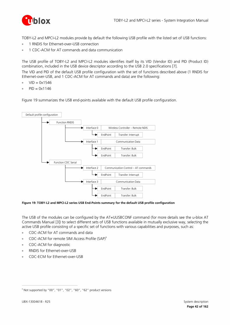
TOBY-L2 and MPCI-L2 series - System Integration Manual
UBX-13004618 - R25 System description
Page 42 of 162
TOBY-L2 and MPCI-L2 modules provide by default the following USB profile with the listed set of USB functions:
1 RNDIS for Ethernet-over-USB connection
1 CDC-ACM for AT commands and data communication
The USB profile of TOBY-L2 and MPCI-L2 modules identifies itself by its VID (Vendor ID) and PID (Product ID) combination, included in the USB device descriptor according to the USB 2.0 specifications [7].
The VID and PID of the default USB profile configuration with the set of functions described above (1 RNDIS for Ethernet-over-USB, and 1 CDC-ACM for AT commands and data) are the following:
VID = 0x1546
PID = 0x1146
Figure 19 summarizes the USB end-points available with the default USB profile configuration.
Default profile configuration
Interface 0 Wireless Controller – Remote NDIS
Interface 1 Communication Data
EndPoint Transfer: Interrupt
EndPoint Transfer: Bulk
EndPoint Transfer: Bulk
Interface 2 Communication Control – AT commands
EndPoint Transfer: Interrupt
Interface 3 Communication Data
EndPoint Transfer: Bulk
EndPoint Transfer: Bulk
Function RNDIS
Function CDC Serial
Figure 19: TOBY-L2 and MPCI-L2 series USB End-Points summary for the default USB profile configuration
The USB of the modules can be configured by the AT+UUSBCONF command (for more details see the u-blox AT Commands Manual [3]) to select different sets of USB functions available in mutually exclusive way, selecting the active USB profile consisting of a specific set of functions with various capabilities and purposes, such as:
CDC-ACM for AT commands and data
CDC-ACM for remote SIM Access Profile (SAP)9
CDC-ACM for diagnostic
RNDIS for Ethernet-over-USB
CDC-ECM for Ethernet-over-USB
9 Not supported by “00”, “01”, “02”, “60”, “62” product versions
TOBY-L2 and MPCI-L2 series - System Integration Manual
UBX-13004618 - R25 System description
Page 43 of 162
For example, the default USB profile configuration which provides 2 functions (1 RNDIS for Ethernet-over-USB, and 1 CDC-ACM for AT commands and data) can be changed by means of the AT+UUSBCONF command switching to a USB profile configuration which provides the following 6 functions:
3 CDC-ACM for AT commands and data
1 CDC-ACM for GNSS tunneling10
1 CDC-ACM for remote SIM Access Profile (SAP)11
1 CDC-ACM for diagnostic
As each USB profile of TOBY-L2 and MPCI-L2 modules identifies itself by its specific VID and PID combination included in the USB device descriptor according to the USB 2.0 specifications [7], the VID and PID combination changes as following by switching the active USB profile configuration to the set of functions described above (3 CDC-ACM for AT commands and data, and 1 CDC-ACM for diagnostic):
VID = 0x1546
PID = 0x1141
Alternatively, as another example, the USB profile configuration can be changed by means of the AT+UUSBCONF command switching to a USB profile configuration which provides the following functions:
1 CDC-ECM for Ethernet-over-USB
3 CDC-ACM for AT commands and data
In case of this USB profile with the set of functions described above (1 CDC-ECM for Ethernet-over-USB, and 3 CDC-ACM for AT commands and data), the VID and PID are the following:
VID = 0x1546
PID = 0x1143
The switch of the active USB profile selected by the AT+UUSBCONF command is not performed immediately. The settings are saved in the non-volatile memory of the module at the power off, triggered by means of the AT+CPWROFF command, and the new configuration is effective at the subsequent reboot of the module.
If the USB is connected to the host before the module is switched on, or if the module is reset (rebooted) with the USB connected to the host, the VID and PID are automatically updated during the boot of the module. First, VID and PID are the following:
VID = 0x1546
PID = 0x1140
This VID and PID combination identifies a USB profile where no USB function described above is available: AT commands must not be sent to the module over the USB profile identified by this VID and PID combination.
Then, after a time period (roughly 20 s, depending on the host / device enumeration timings), the VID and PID are updated to the ones related to the USB profile selected by the AT+UUSBCONF command.
For more details regarding the TOBY-L2 and MPCI-L2 series modules USB configurations and capabilities, see the u-blox AT Commands Manual [3], +UUSBCONF AT command.
10
Not supported by “00”, “01”, “02”, “03”, “60”, “62” product versions 11
Not supported by “00”, “01”, “02”, “60”, “62” product versions
TOBY-L2 and MPCI-L2 series - System Integration Manual
UBX-13004618 - R25 System description
Page 44 of 162
1.9.1.2 USB in Windows
USB drivers are provided for Windows operating system platforms and should be properly installed / enabled by following the step-by-step instructions available in the EVK-L2x User Guide [4] or in the Windows Embedded OS USB Driver Installation Application Note [5].
USB drivers are available for the following operating system platforms:
Windows Vista
Windows 7
Windows 8
Windows 8.1
Windows 10
Windows Embedded CE 6.0
Windows Embedded Compact 7
Windows Embedded Compact 2013
The module firmware can be upgraded over the USB interface by means of the FOAT feature, or using the u-blox EasyFlash tool (for more details see Firmware Update Application Note [6]).
1.9.1.3 USB in Linux/Android
It is not required to install a specific driver for each Linux-based or Android-based operating system (OS) to use the module USB interface, which is compatible with standard Linux/Android USB kernel drivers.
The full capability and configuration of the module USB interface can be reported by running “lsusb –v” or an equivalent command available in the host operating system when the module is connected.
1.9.1.4 USB and power saving
The modules automatically enter the USB suspended state when the device has observed no bus traffic for a specific time period according to the USB 2.0 specification [7]. In suspended state, the module maintains any USB internal status as device. In addition, the module enters the suspended state when the hub port it is attached to is disabled. This is referred to as USB selective suspend.
If the USB is suspended and a power saving configuration is enabled by the AT+UPSV command, the module automatically enters the low power idle-mode whenever possible but it wakes up to active-mode according to any required activity related to the network (e.g. the periodic paging reception described in section 1.5.1.5) or any other required activity related to the functions / interfaces of the module.
The USB exits suspend mode when there is bus activity. If the USB is connected and not suspended, the module is forced to stay in active-mode, therefore the AT+UPSV settings are overruled but they have effect on the power saving configuration of the other interfaces.
The modules are capable of USB remote wake-up signaling: i.e. it may request the host to exit suspend mode or selective suspend by using electrical signaling to indicate remote wake-up, for example due to incoming call, URCs, data reception on a socket. The remote wake-up signaling notifies the host that it should resume from its suspended mode, if necessary, and service the external event. Remote wake-up is accomplished using electrical signaling described in the USB 2.0 specifications [7].
For the module current consumption description with power saving enabled and USB suspended, or with power saving disabled and USB not suspended, see the sections 1.5.1.5, 1.5.1.6 and the TOBY-L2 Data Sheet [1] or the MPCI-L2 Data Sheet [2].
TOBY-L2 and MPCI-L2 series - System Integration Manual
UBX-13004618 - R25 System description
Page 45 of 162
1.9.2 Asynchronous serial interface (UART)
The UART interface is not available on MPCI-L2 series modules.
The UART interface is not supported by TOBY-L2 series modules “00” product versions.
1.9.2.1 UART features
The UART interface is a 9-wire 1.8 V unbalanced asynchronous serial interface (UART) that can be connected to an application host processor for AT commands and data communication.
The module firmware can be upgraded over the UART interface by means of the Firmware upgrade over AT (FOAT) feature only: for more details see section 1.15 and Firmware Update Application Note [6].
UART interface provides RS-232 functionality conforming to the ITU-T V.24 Recommendation [8], with CMOS compatible signal levels: 0 V for low data bit or ON state, and 1.8 V for high data bit or OFF state (for detailed electrical characteristics see TOBY-L2 Data Sheet [1]), providing:
data lines (RXD as output, TXD as input),
hardware flow control lines (CTS as output, RTS as input),
modem status and control lines (DTR as input, DSR as output, DCD as output, RI as output).
TOBY-L2 modules are designed to operate as LTE/3G/2G cellular modems, i.e. as the data circuit-terminating equipment (DCE) according to the ITU-T V.24 Recommendation [8]. A host application processor connected to the module through the UART interface represents the data terminal equipment (DTE).
UART signal names of TOBY-L2 modules conform to the ITU-T V.24 Recommendation [8]: e.g. TXD line represents data transmitted by the DTE (host processor output) and received by the DCE (module input).
The UART interface is controlled and operated with:
AT commands according to 3GPP TS 27.007 [9], 3GPP TS 27.005 [10], 3GPP TS 27.010 [11]
u-blox AT commands
For the complete list of supported AT commands and their syntax see u-blox AT Commands Manual [3], and in particular for the UART configuration see the +IPR, +ICF, +IFC, &K, \Q, +UPSV AT commands.
Flow control handshakes are supported by the UART interface and can be set by appropriate AT commands (see u-blox AT Commands Manual [3], &K, +IFC, \Q AT commands): hardware flow control (over the RTS / CTS lines), software flow control (XON/XOFF), or none flow control.
Hardware flow control is enabled by default.
Software flow control is not supported by “00”, “01”, “60” and TOBY-L201-02S product versions.
The one-shot autobauding is supported: the automatic baud rate detection is performed only once, at module start up. After the detection, the module works at the detected baud rate and the baud rate can only be changed by AT command (see u-blox AT Commands Manual [3], +IPR).
One-shot automatic baud rate recognition (autobauding) is enabled by default.
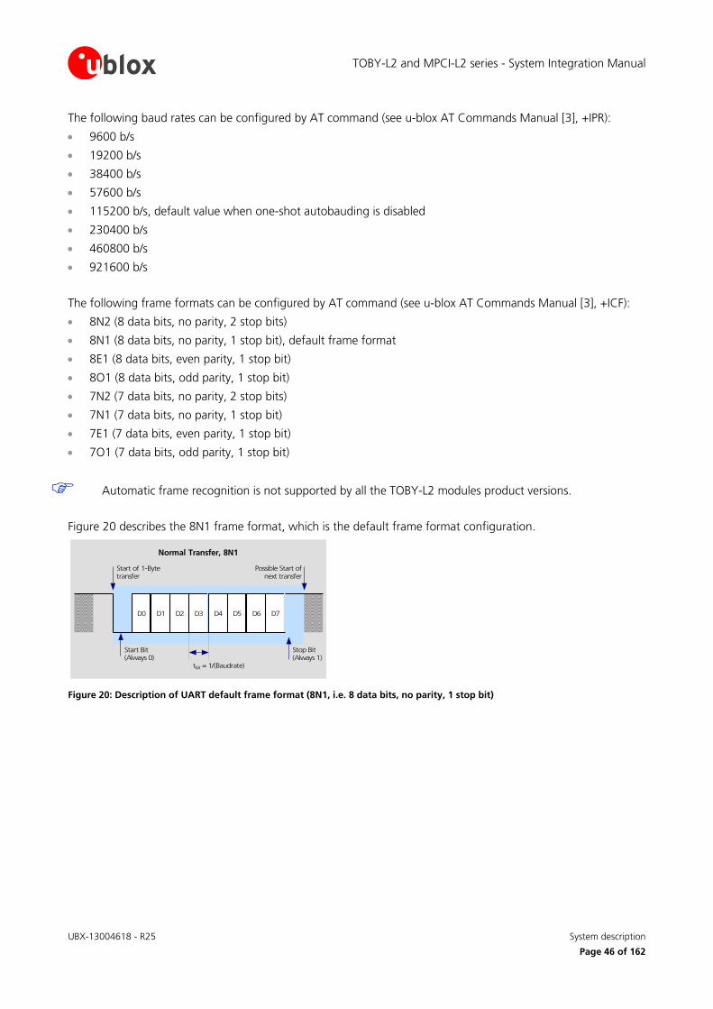
TOBY-L2 and MPCI-L2 series - System Integration Manual
UBX-13004618 - R25 System description
Page 46 of 162
The following baud rates can be configured by AT command (see u-blox AT Commands Manual [3], +IPR):
9600 b/s
19200 b/s
38400 b/s
57600 b/s
115200 b/s, default value when one-shot autobauding is disabled
230400 b/s
460800 b/s
921600 b/s
The following frame formats can be configured by AT command (see u-blox AT Commands Manual [3], +ICF):
8N2 (8 data bits, no parity, 2 stop bits)
8N1 (8 data bits, no parity, 1 stop bit), default frame format
8E1 (8 data bits, even parity, 1 stop bit)
8O1 (8 data bits, odd parity, 1 stop bit)
7N2 (7 data bits, no parity, 2 stop bits)
7N1 (7 data bits, no parity, 1 stop bit)
7E1 (7 data bits, even parity, 1 stop bit)
7O1 (7 data bits, odd parity, 1 stop bit)
Automatic frame recognition is not supported by all the TOBY-L2 modules product versions.
Figure 20 describes the 8N1 frame format, which is the default frame format configuration.
D0 D1 D2 D3 D4 D5 D6 D7
Start of 1-Bytetransfer
Start Bit(Always 0)
Possible Start ofnext transfer
Stop Bit(Always 1)
tbit = 1/(Baudrate)
Normal Transfer, 8N1
Figure 20: Description of UART default frame format (8N1, i.e. 8 data bits, no parity, 1 stop bit)
TOBY-L2 and MPCI-L2 series - System Integration Manual
UBX-13004618 - R25 System description
Page 47 of 162
1.9.2.2 UART interface configuration
The UART interface of TOBY-L2 series modules is available as AT command interface with the default configuration described in Table 11 (for more details and information about further settings, see the u-blox AT Commands Manual [3]).
Interface AT Settings Comments
UART interface AT interface: enabled AT command interface is enabled by default on the UART physical interface
AT+IPR=0 One-shot autobauding enabled by default on the modules
AT+ICF=3,1 8N1 frame format enabled by default
AT&K3 HW flow control enabled by default
AT&S1 DSR line (Circuit 107 in ITU-T V.24) set ON in data mode12
and set OFF in command mode17
AT&D1 Upon an ON-to-OFF transition of DTR line (Circuit 108/2 in ITU-T V.24), the module (DCE) enters online command mode
17 and issues an OK result code
AT&C1 DCD line (Circuit 109 in ITU-T V.24) changes in accordance with the Carrier detect status; ON if the Carrier is detected, OFF otherwise
MUX protocol: disabled Multiplexing mode is disabled by default and it can be enabled by AT+CMUX command. For more details, see the Mux Implementation Application Note [12].
The following virtual channels are defined:
Channel 0: control channel
Channel 1 – 5: AT commands / data connection
Table 11: Default UART interface configuration
1.9.2.3 UART signals behavior
At the module switch-on, before the UART interface initialization (as described in the power-on sequence reported in Figure 14), each pin is first tri-stated and then is set to its relative internal reset state
13. At the end of
the boot sequence, the UART interface is initialized, the module is by default in active-mode, and the UART interface is enabled as AT commands interface.
The configuration and the behavior of the UART signals after the boot sequence are described below. See section 1.4 for definition and description of module operating modes referred to in this section.
RXD signal behavior
The module data output line (RXD) is set by default to the OFF state (high level) at UART initialization. The module holds RXD in the OFF state until the module does not transmit some data.
TXD signal behavior
The module data input line (TXD) is set by default to the OFF state (high level) at UART initialization. The TXD line is then held by the module in the OFF state if the line is not activated by the DTE: an active pull-up is enabled inside the module on the TXD input.
12
For the definition of the interface data mode, command mode and online command mode see the u-blox AT Commands Manual [3] 13
See the pin description table in the TOBY-L2 series Data Sheet [1]
TOBY-L2 and MPCI-L2 series - System Integration Manual
UBX-13004618 - R25 System description
Page 48 of 162
CTS signal behavior
The module hardware flow control output (CTS line) is set to the ON state (low level) at UART initialization.
If the hardware flow control is enabled, as it is by default, the CTS line indicates when the UART interface is enabled (data can be received): the module drives the CTS line to the ON state or to the OFF state when it is either able or not able to accept data from the DTE over the UART (for example see section 1.9.2.4, Figure 23).
The module guarantees the reception of characters when the CTS line is set to the ON state, and the module is also able to accept up to 3 characters after the CTS line is set to the OFF state.
If hardware flow control is enabled, then when the CTS line is OFF it does not necessarily mean that the module is in low power idle-mode, but only that the UART is not enabled, as the module could be forced to stay in active-mode for other activities, e.g. related to the network or related to other interfaces.
If hardware flow control is enabled and the multiplexer protocol is active, then the CTS line state is mapped to FCon / FCoff MUX command for flow control matters outside the power saving configuration while the physical CTS line is still used as a UART power state indicator (see the Mux Implementation Application Note [12]).
The CTS hardware flow control setting can be changed by AT commands (for more details, see the u-blox AT Commands Manual [3], AT&K, AT\Q, AT+IFC AT commands).
If the hardware flow control is not enabled, the CTS line still indicates when the UART interface is enabled, as it does when hardware flow control is enabled. The module drives the CTS line to the ON state or to the OFF state when it is either able or not able to accept data from the DTE over the UART interface.
When the power saving configuration is enabled by AT+UPSV command and the hardware flow-control is not implemented in the DTE/DCE connection, data sent by the DTE can be lost: the first character sent when the module is in low power idle-mode will not be a valid communication character (see section 1.9.2.4 and in particular the sub-section “Wake up via data reception” for further details).
RTS signal behavior
The hardware flow control input (RTS line) is set by default to the OFF state (high level) at UART initialization. The module then holds the RTS line in the OFF state if the line is not activated by the DTE: an active pull-up is enabled inside the module on the RTS input.
If the HW flow control is enabled, as it is by default, the module monitors the RTS line to detect permission from the DTE to send data to the DTE itself. If the RTS line is set to the OFF state, any on-going data transmission from the module is interrupted until the RTS line changes to the ON state.
The DTE must still be able to accept a certain number of characters after the RTS line is set to the OFF state: the module guarantees the transmission interruption within two characters from RTS state change.
The module behavior according to the RTS hardware flow control status can be configured by AT commands (for more details, see the u-blox AT Commands Manual [3], AT&K, AT\Q, AT+IFC AT commands).
If AT+UPSV=2 is set and HW flow control is disabled, the module monitors the RTS line to manage the power saving configuration (for more details, see section 1.9.2.4 and u-blox AT Commands Manual [3], AT+UPSV):
When an OFF-to-ON transition occurs on the RTS input, the UART is enabled and the module is forced to active-mode; after ~5 ms from the transition the switch is completed and data can be received without loss. The module cannot enter low power idle-mode and the UART is keep enabled as long as the RTS input line is held in the ON state
If the RTS input line is set to the OFF state by the DTE, the UART is disabled (held in low power mode) and the module automatically enters low power idle-mode whenever possible
TOBY-L2 and MPCI-L2 series - System Integration Manual
UBX-13004618 - R25 System description
Page 49 of 162
DSR signal behavior
If AT&S1 is set, as it is by default, the DSR module output line is set by default to the OFF state (high level) at UART initialization. The DSR line is then set to the OFF state when the module is in command mode
14 or in
online command mode14 and is set to the ON state when the module is in data mode
14.
If AT&S0 is set, the DSR module output line is set by default to the ON state (low level) at UART initialization and is then always held in the ON state.
DTR signal behavior
The DTR module input line is set by default to the OFF state (high level) at UART initialization. The module then holds the DTR line in the OFF state if the line is not activated by the DTE: an active pull-up is enabled inside the module on the DTR input.
Module behavior according to DTR status can be changed by AT command configuration (for more details see the u-blox AT Commands Manual [3], &D AT command description).
If AT+UPSV=3 is set, the DTR line is monitored by the module to manage the power saving configuration (for more details, see section 1.9.2.4 and u-blox AT Commands Manual [3], AT+UPSV):
When an OFF-to-ON transition occurs on the DTR input, the UART is enabled and the module is forced to active-mode; after ~5 ms from the transition, the switch is completed and data can be received without loss. The module cannot enter low power idle-mode and the UART is keep enabled as long as the DTR input line is held in the ON state
If the DTR input line is set to the OFF state by the DTE, the UART is disabled (held in low power mode) and the module automatically enters low power idle-mode whenever possible
DCD signal behavior
If AT&C1 is set, as it is by default, the DCD module output line is set by default to the OFF state (high level) at UART initialization. The module then sets the DCD line according to the carrier detect status: ON if the carrier is detected, OFF otherwise.
In case of voice calls, DCD is set to the ON state when the call is established.
If a Packet Switched Data call occurs before activating the PPP protocol (data mode), a dial-up application must provide the ATD*99***<context_number># to the module: with this command the module switches from command mode
14 to data mode
14 and can accept PPP packets. The module sets the DCD line to the ON state,
then answers with a CONNECT to confirm the ATD*99 command. The DCD ON is not related to the context activation but with the data mode.
The DCD is set to ON during the execution of the +CMGS, +CMGW, +USOWR, +USODL AT commands requiring input data from the DTE: the DCD line is set to the ON state as soon as the switch to binary/text input mode is completed and the prompt is issued; DCD line is set to OFF as soon as the input mode is interrupted or completed (for more details see the u-blox AT Commands Manual [3]).
The DCD line is kept in the ON state, even during the online command mode14, to indicate that the data
call is still established even if suspended, while if the module enters command mode14, the DSR line is set
to the OFF state. For more details see DSR signal behavior description.
For scenarios when the DCD line setting is requested for different reasons (e.g. SMS texting during online command mode
14), the DCD line changes to guarantee the correct behavior for all the scenarios. For
example, in case of SMS texting in online command mode14, if the data call is released, DCD is kept ON till
the SMS command execution is completed (even if the data call release would request DCD set OFF).
If AT&C0 is set, the DCD module output line is set by default to the ON state (low level) at UART initialization and is then always held in the ON state.
14
For the definition of the interface data mode, command mode and online command mode see the u-blox AT Commands Manual [3]
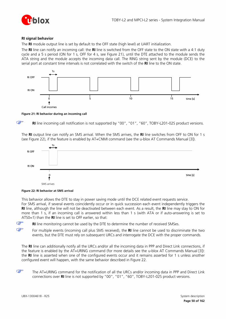
TOBY-L2 and MPCI-L2 series - System Integration Manual
UBX-13004618 - R25 System description
Page 50 of 162
RI signal behavior
The RI module output line is set by default to the OFF state (high level) at UART initialization.
The RI line can notify an incoming call: the RI line is switched from the OFF state to the ON state with a 4:1 duty cycle and a 5 s period (ON for 1 s, OFF for 4 s, see Figure 21), until the DTE attached to the module sends the ATA string and the module accepts the incoming data call. The RING string sent by the module (DCE) to the serial port at constant time intervals is not correlated with the switch of the RI line to the ON state.
Figure 21: RI behavior during an incoming call
RI line incoming call notification is not supported by “00”, “01”, “60”, TOBY-L201-02S product versions.
The RI output line can notify an SMS arrival. When the SMS arrives, the RI line switches from OFF to ON for 1 s (see Figure 22), if the feature is enabled by AT+CNMI command (see the u-blox AT Commands Manual [3]).
Figure 22: RI behavior at SMS arrival
This behavior allows the DTE to stay in power saving mode until the DCE related event requests service. For SMS arrival, if several events coincidently occur or in quick succession each event independently triggers the RI line, although the line will not be deactivated between each event. As a result, the RI line may stay to ON for more than 1 s, if an incoming call is answered within less than 1 s (with ATA or if auto-answering is set to ATS0=1) than the RI line is set to OFF earlier, so that:
RI line monitoring cannot be used by the DTE to determine the number of received SMSes.
For multiple events (incoming call plus SMS received), the RI line cannot be used to discriminate the two events, but the DTE must rely on subsequent URCs and interrogate the DCE with the proper commands.
The RI line can additionally notify all the URCs and/or all the incoming data in PPP and Direct Link connections, if the feature is enabled by the AT+URING command (for more details see the u-blox AT Commands Manual [3]): the RI line is asserted when one of the configured events occur and it remains asserted for 1 s unless another configured event will happen, with the same behavior described in Figure 22.
The AT+URING command for the notification of all the URCs and/or incoming data in PPP and Direct Link connections over RI line is not supported by “00”, “01”, “60”, TOBY-L201-02S product versions.
SMS arrives
time [s] 0
RI ON
RI OFF
1s
time [s] 0
RI ON
RI OFF
1s
1s
time [s]151050
RI ON
RI OFF
Call incomes
1s
time [s]151050
RI ON
RI OFF
Call incomes
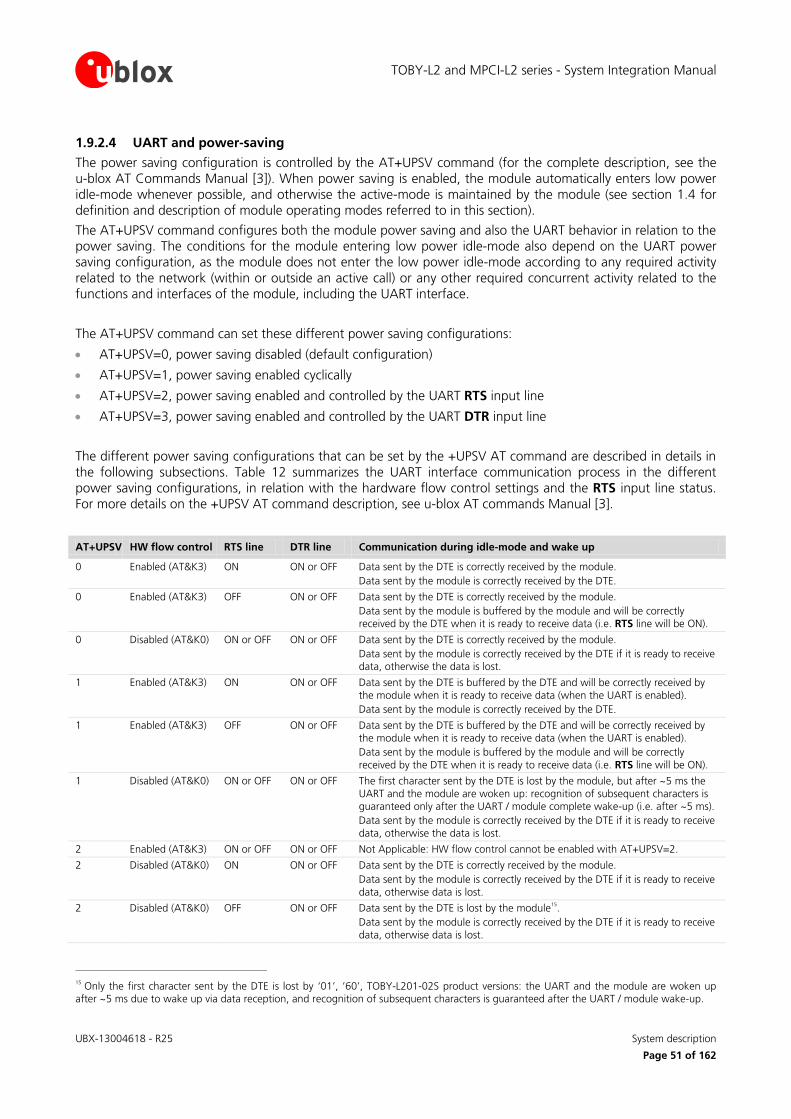
TOBY-L2 and MPCI-L2 series - System Integration Manual
UBX-13004618 - R25 System description
Page 51 of 162
1.9.2.4 UART and power-saving
The power saving configuration is controlled by the AT+UPSV command (for the complete description, see the u-blox AT Commands Manual [3]). When power saving is enabled, the module automatically enters low power idle-mode whenever possible, and otherwise the active-mode is maintained by the module (see section 1.4 for definition and description of module operating modes referred to in this section).
The AT+UPSV command configures both the module power saving and also the UART behavior in relation to the power saving. The conditions for the module entering low power idle-mode also depend on the UART power saving configuration, as the module does not enter the low power idle-mode according to any required activity related to the network (within or outside an active call) or any other required concurrent activity related to the functions and interfaces of the module, including the UART interface.
The AT+UPSV command can set these different power saving configurations:
AT+UPSV=0, power saving disabled (default configuration)
AT+UPSV=1, power saving enabled cyclically
AT+UPSV=2, power saving enabled and controlled by the UART RTS input line
AT+UPSV=3, power saving enabled and controlled by the UART DTR input line
The different power saving configurations that can be set by the +UPSV AT command are described in details in the following subsections. Table 12 summarizes the UART interface communication process in the different power saving configurations, in relation with the hardware flow control settings and the RTS input line status. For more details on the +UPSV AT command description, see u-blox AT commands Manual [3].
AT+UPSV HW flow control RTS line DTR line Communication during idle-mode and wake up
0 Enabled (AT&K3) ON ON or OFF Data sent by the DTE is correctly received by the module.
Data sent by the module is correctly received by the DTE.
0 Enabled (AT&K3) OFF ON or OFF Data sent by the DTE is correctly received by the module.
Data sent by the module is buffered by the module and will be correctly received by the DTE when it is ready to receive data (i.e. RTS line will be ON).
0 Disabled (AT&K0) ON or OFF ON or OFF Data sent by the DTE is correctly received by the module.
Data sent by the module is correctly received by the DTE if it is ready to receive data, otherwise the data is lost.
1 Enabled (AT&K3) ON ON or OFF Data sent by the DTE is buffered by the DTE and will be correctly received by
the module when it is ready to receive data (when the UART is enabled).
Data sent by the module is correctly received by the DTE.
1 Enabled (AT&K3) OFF ON or OFF Data sent by the DTE is buffered by the DTE and will be correctly received by the module when it is ready to receive data (when the UART is enabled).
Data sent by the module is buffered by the module and will be correctly
received by the DTE when it is ready to receive data (i.e. RTS line will be ON).
1 Disabled (AT&K0) ON or OFF ON or OFF The first character sent by the DTE is lost by the module, but after ~5 ms the
UART and the module are woken up: recognition of subsequent characters is guaranteed only after the UART / module complete wake-up (i.e. after ~5 ms).
Data sent by the module is correctly received by the DTE if it is ready to receive
data, otherwise the data is lost.
2 Enabled (AT&K3) ON or OFF ON or OFF Not Applicable: HW flow control cannot be enabled with AT+UPSV=2.
2 Disabled (AT&K0) ON ON or OFF Data sent by the DTE is correctly received by the module.
Data sent by the module is correctly received by the DTE if it is ready to receive
data, otherwise data is lost.
2 Disabled (AT&K0) OFF ON or OFF Data sent by the DTE is lost by the module15
.
Data sent by the module is correctly received by the DTE if it is ready to receive data, otherwise data is lost.
15
Only the first character sent by the DTE is lost by ‘01’, ‘60’, TOBY-L201-02S product versions: the UART and the module are woken up after ~5 ms due to wake up via data reception, and recognition of subsequent characters is guaranteed after the UART / module wake-up.
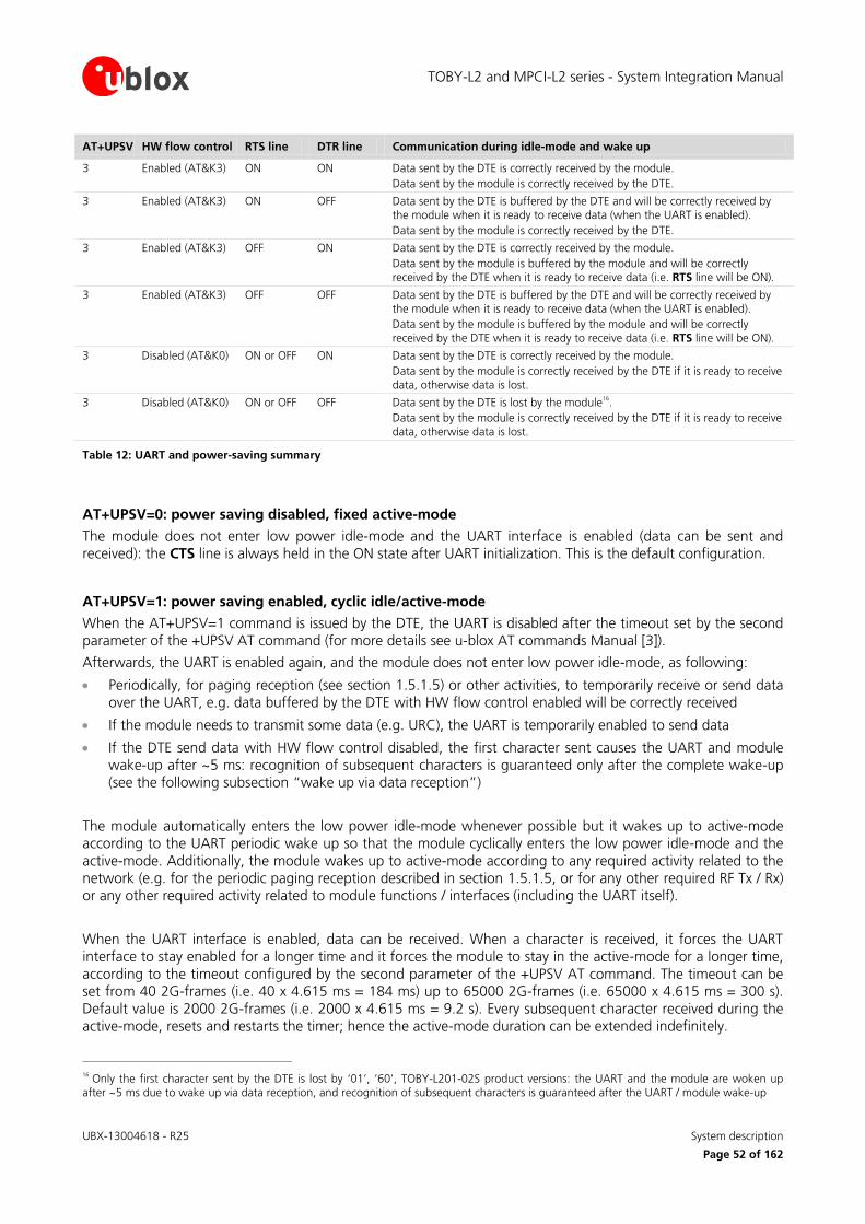
TOBY-L2 and MPCI-L2 series - System Integration Manual
UBX-13004618 - R25 System description
Page 52 of 162
AT+UPSV HW flow control RTS line DTR line Communication during idle-mode and wake up
3 Enabled (AT&K3) ON ON Data sent by the DTE is correctly received by the module.
Data sent by the module is correctly received by the DTE.
3 Enabled (AT&K3) ON OFF Data sent by the DTE is buffered by the DTE and will be correctly received by the module when it is ready to receive data (when the UART is enabled).
Data sent by the module is correctly received by the DTE.
3 Enabled (AT&K3) OFF ON Data sent by the DTE is correctly received by the module.
Data sent by the module is buffered by the module and will be correctly received by the DTE when it is ready to receive data (i.e. RTS line will be ON).
3 Enabled (AT&K3) OFF OFF Data sent by the DTE is buffered by the DTE and will be correctly received by the module when it is ready to receive data (when the UART is enabled).
Data sent by the module is buffered by the module and will be correctly received by the DTE when it is ready to receive data (i.e. RTS line will be ON).
3 Disabled (AT&K0) ON or OFF ON Data sent by the DTE is correctly received by the module.
Data sent by the module is correctly received by the DTE if it is ready to receive data, otherwise data is lost.
3 Disabled (AT&K0) ON or OFF OFF Data sent by the DTE is lost by the module16
.
Data sent by the module is correctly received by the DTE if it is ready to receive
data, otherwise data is lost.
Table 12: UART and power-saving summary
AT+UPSV=0: power saving disabled, fixed active-mode
The module does not enter low power idle-mode and the UART interface is enabled (data can be sent and received): the CTS line is always held in the ON state after UART initialization. This is the default configuration.
AT+UPSV=1: power saving enabled, cyclic idle/active-mode
When the AT+UPSV=1 command is issued by the DTE, the UART is disabled after the timeout set by the second parameter of the +UPSV AT command (for more details see u-blox AT commands Manual [3]).
Afterwards, the UART is enabled again, and the module does not enter low power idle-mode, as following:
Periodically, for paging reception (see section 1.5.1.5) or other activities, to temporarily receive or send data over the UART, e.g. data buffered by the DTE with HW flow control enabled will be correctly received
If the module needs to transmit some data (e.g. URC), the UART is temporarily enabled to send data
If the DTE send data with HW flow control disabled, the first character sent causes the UART and module wake-up after ~5 ms: recognition of subsequent characters is guaranteed only after the complete wake-up (see the following subsection “wake up via data reception”)
The module automatically enters the low power idle-mode whenever possible but it wakes up to active-mode according to the UART periodic wake up so that the module cyclically enters the low power idle-mode and the active-mode. Additionally, the module wakes up to active-mode according to any required activity related to the network (e.g. for the periodic paging reception described in section 1.5.1.5, or for any other required RF Tx / Rx) or any other required activity related to module functions / interfaces (including the UART itself).
When the UART interface is enabled, data can be received. When a character is received, it forces the UART interface to stay enabled for a longer time and it forces the module to stay in the active-mode for a longer time, according to the timeout configured by the second parameter of the +UPSV AT command. The timeout can be set from 40 2G-frames (i.e. 40 x 4.615 ms = 184 ms) up to 65000 2G-frames (i.e. 65000 x 4.615 ms = 300 s). Default value is 2000 2G-frames (i.e. 2000 x 4.615 ms = 9.2 s). Every subsequent character received during the active-mode, resets and restarts the timer; hence the active-mode duration can be extended indefinitely.
16
Only the first character sent by the DTE is lost by ‘01’, ‘60’, TOBY-L201-02S product versions: the UART and the module are woken up after ~5 ms due to wake up via data reception, and recognition of subsequent characters is guaranteed after the UART / module wake-up
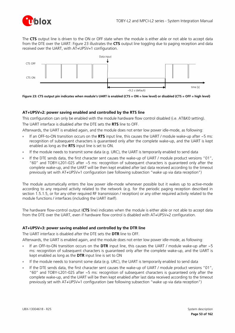
TOBY-L2 and MPCI-L2 series - System Integration Manual
UBX-13004618 - R25 System description
Page 53 of 162
The CTS output line is driven to the ON or OFF state when the module is either able or not able to accept data from the DTE over the UART: Figure 23 illustrates the CTS output line toggling due to paging reception and data received over the UART, with AT+UPSV=1 configuration.
time [s]~9.2 s (default)
Data input
CTS ON
CTS OFF
Figure 23: CTS output pin indicates when module’s UART is enabled (CTS = ON = low level) or disabled (CTS = OFF = high level)
AT+UPSV=2: power saving enabled and controlled by the RTS line
This configuration can only be enabled with the module hardware flow control disabled (i.e. AT&K0 setting).
The UART interface is disabled after the DTE sets the RTS line to OFF.
Afterwards, the UART is enabled again, and the module does not enter low power idle-mode, as following:
If an OFF-to-ON transition occurs on the RTS input line, this causes the UART / module wake-up after ~5 ms: recognition of subsequent characters is guaranteed only after the complete wake-up, and the UART is kept enabled as long as the RTS input line is set to ON.
If the module needs to transmit some data (e.g. URC), the UART is temporarily enabled to send data
If the DTE sends data, the first character sent causes the wake-up of UART / module product versions “01”, “60” and TOBY-L201-02S after ~5 ms: recognition of subsequent characters is guaranteed only after the complete wake-up, and the UART will be then kept enabled after last data received according to the timeout previously set with AT+UPSV=1 configuration (see following subsection “wake up via data reception”)
The module automatically enters the low power idle-mode whenever possible but it wakes up to active-mode according to any required activity related to the network (e.g. for the periodic paging reception described in section 1.5.1.5, or for any other required RF transmission / reception) or any other required activity related to the module functions / interfaces (including the UART itself).
The hardware flow-control output (CTS line) indicates when the module is either able or not able to accept data from the DTE over the UART, even if hardware flow control is disabled with AT+UPSV=2 configuration.
AT+UPSV=3: power saving enabled and controlled by the DTR line
The UART interface is disabled after the DTE sets the DTR line to OFF.
Afterwards, the UART is enabled again, and the module does not enter low power idle-mode, as following:
If an OFF-to-ON transition occurs on the DTR input line, this causes the UART / module wake-up after ~5 ms: recognition of subsequent characters is guaranteed only after the complete wake-up, and the UART is kept enabled as long as the DTR input line is set to ON
If the module needs to transmit some data (e.g. URC), the UART is temporarily enabled to send data
If the DTE sends data, the first character sent causes the wake-up of UART / module product versions “01”, “60” and TOBY-L201-02S after ~5 ms: recognition of subsequent characters is guaranteed only after the complete wake-up, and the UART will be then kept enabled after last data received according to the timeout previously set with AT+UPSV=1 configuration (see following subsection “wake up via data reception”)
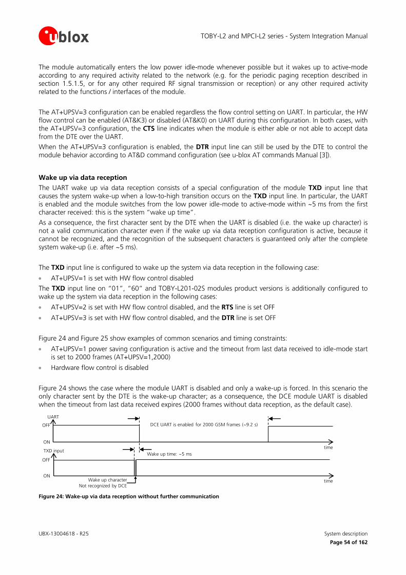
TOBY-L2 and MPCI-L2 series - System Integration Manual
UBX-13004618 - R25 System description
Page 54 of 162
The module automatically enters the low power idle-mode whenever possible but it wakes up to active-mode according to any required activity related to the network (e.g. for the periodic paging reception described in section 1.5.1.5, or for any other required RF signal transmission or reception) or any other required activity related to the functions / interfaces of the module.
The AT+UPSV=3 configuration can be enabled regardless the flow control setting on UART. In particular, the HW flow control can be enabled (AT&K3) or disabled (AT&K0) on UART during this configuration. In both cases, with the AT+UPSV=3 configuration, the CTS line indicates when the module is either able or not able to accept data from the DTE over the UART.
When the AT+UPSV=3 configuration is enabled, the DTR input line can still be used by the DTE to control the module behavior according to AT&D command configuration (see u-blox AT commands Manual [3]).
Wake up via data reception
The UART wake up via data reception consists of a special configuration of the module TXD input line that causes the system wake-up when a low-to-high transition occurs on the TXD input line. In particular, the UART is enabled and the module switches from the low power idle-mode to active-mode within ~5 ms from the first character received: this is the system “wake up time”.
As a consequence, the first character sent by the DTE when the UART is disabled (i.e. the wake up character) is not a valid communication character even if the wake up via data reception configuration is active, because it cannot be recognized, and the recognition of the subsequent characters is guaranteed only after the complete system wake-up (i.e. after ~5 ms).
The TXD input line is configured to wake up the system via data reception in the following case:
AT+UPSV=1 is set with HW flow control disabled
The TXD input line on “01”, “60” and TOBY-L201-02S modules product versions is additionally configured to wake up the system via data reception in the following cases:
AT+UPSV=2 is set with HW flow control disabled, and the RTS line is set OFF
AT+UPSV=3 is set with HW flow control disabled, and the DTR line is set OFF
Figure 24 and Figure 25 show examples of common scenarios and timing constraints:
AT+UPSV=1 power saving configuration is active and the timeout from last data received to idle-mode start is set to 2000 frames (AT+UPSV=1,2000)
Hardware flow control is disabled
Figure 24 shows the case where the module UART is disabled and only a wake-up is forced. In this scenario the only character sent by the DTE is the wake-up character; as a consequence, the DCE module UART is disabled when the timeout from last data received expires (2000 frames without data reception, as the default case).
Wake up character
Not recognized by DCE
OFF
ON
DCE UART is enabled for 2000 GSM frames (~9.2 s)
time
Wake up time: ~5 ms
time
TXD input
UART
OFF
ON
Figure 24: Wake-up via data reception without further communication
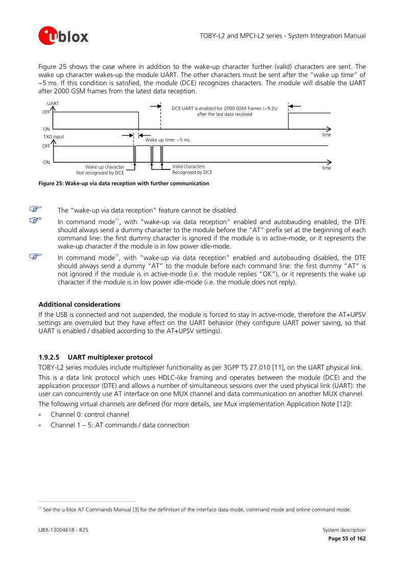
TOBY-L2 and MPCI-L2 series - System Integration Manual
UBX-13004618 - R25 System description
Page 55 of 162
Figure 25 shows the case where in addition to the wake-up character further (valid) characters are sent. The wake up character wakes-up the module UART. The other characters must be sent after the “wake up time” of ~5 ms. If this condition is satisfied, the module (DCE) recognizes characters. The module will disable the UART after 2000 GSM frames from the latest data reception.
Wake up character Not recognized by DCE
Valid characters
Recognized by DCE
DCE UART is enabled for 2000 GSM frames (~9.2s) after the last data received
time Wake up time: ~5 ms
time
OFF
ON
TXD input
UART
OFF
ON
Figure 25: Wake-up via data reception with further communication
The “wake-up via data reception” feature cannot be disabled.
In command mode17
, with “wake-up via data reception” enabled and autobauding enabled, the DTE should always send a dummy character to the module before the “AT” prefix set at the beginning of each command line: the first dummy character is ignored if the module is in active-mode, or it represents the wake-up character if the module is in low power idle-mode.
In command mode17, with “wake-up via data reception” enabled and autobauding disabled, the DTE
should always send a dummy “AT” to the module before each command line: the first dummy “AT” is not ignored if the module is in active-mode (i.e. the module replies “OK”), or it represents the wake up character if the module is in low power idle-mode (i.e. the module does not reply).
Additional considerations
If the USB is connected and not suspended, the module is forced to stay in active-mode, therefore the AT+UPSV settings are overruled but they have effect on the UART behavior (they configure UART power saving, so that UART is enabled / disabled according to the AT+UPSV settings).
1.9.2.5 UART multiplexer protocol
TOBY-L2 series modules include multiplexer functionality as per 3GPP TS 27.010 [11], on the UART physical link.
This is a data link protocol which uses HDLC-like framing and operates between the module (DCE) and the application processor (DTE) and allows a number of simultaneous sessions over the used physical link (UART): the user can concurrently use AT interface on one MUX channel and data communication on another MUX channel.
The following virtual channels are defined (for more details, see Mux implementation Application Note [12]):
Channel 0: control channel
Channel 1 – 5: AT commands / data connection
17
See the u-blox AT Commands Manual [3] for the definition of the interface data mode, command mode and online command mode.
TOBY-L2 and MPCI-L2 series - System Integration Manual
UBX-13004618 - R25 System description
Page 56 of 162
1.9.3 DDC (I2C) interface
The I2C bus compatible Display Data Channel interface is not available on the MPCI-L2 series modules.
The I2C bus compatible Display Data Channel interface is not supported by the TOBY-L2 series modules
“00”, “01”, “60” and TOBY-L201-02S product versions.
The SDA and SCL pins of TOBY-L2 series modules represent an I2C bus compatible Display Data Channel (DDC)
interface for the communication with external I2C devices as audio codecs: an I
2C master can communicate with
more I2C slaves in accordance to the I
2C bus specifications [13].
The AT commands interface is not available on the DDC (I2C) interface.
DDC (I2C) slave-mode operation is not supported: the TOBY-L2 series module can act as I
2C master only.
The DDC (I2C) interface pads of the module, serial data (SDA) and serial clock (SCL), are open drain output and
external pull up resistors must be used conforming to the I2C bus specifications [13].
1.9.4 Secure Digital Input Output interface (SDIO)
Secure Digital Input Output interface is not available on MPCI-L2 series modules.
Secure Digital Input Output interface is not supported by TOBY-L2 “00”, “01”, “60” product versions.
TOBY-L2 series modules include a 4-bit Secure Digital Input Output interface (SDIO_D0, SDIO_D1, SDIO_D2, SDIO_D3, SDIO_CLK, SDIO_CMD) designed to communicate with an external u-blox short range Wi-Fi module: the TOBY-L2 cellular module acts as an SDIO host controller which can communicate over the SDIO bus with a compatible u-blox short range Wi-Fi module acting as SDIO device.
The SDIO interface is the only one interface of TOBY-L2 series modules dedicated for communication between the u-blox cellular module and the u-blox short range Wi-Fi module. The AT commands interface is not available on the SDIO interface of TOBY-L2 series modules.
The SDIO interface supports 50 MHz bus clock frequency, which allows a data throughput of 200 Mb/s.
Combining a u-blox cellular module with a u-blox short range communication module gives designers full access to the Wi-Fi module directly via the cellular module, so that a second interface connected to the Wi-Fi module is not necessary. AT commands via the AT interfaces of the cellular module (UART, USB) allows a full control of the Wi-Fi module from any host processor, because Wi-Fi control messages are relayed to the Wi-Fi module via the dedicated SDIO interface (for more details, see the Wi-Fi AT commands in the u-blox AT Commands Manual [3]).
u-blox has implemented special features in the cellular modules to ease the design effort for the integration of a u-blox cellular module with a u-blox short range Wi-Fi module to provide Router functionality (for more details, see the Wi-Fi / Cellular Integration Application Note [15]).
Additional custom function over GPIO pins is designed to improve the integration with u-blox Wi-Fi modules:
Wi-Fi enable Switch-on / switch-off the Wi-Fi
GPIOs are not supported by TOBY-L2 “00”, “01” and “60” product versions, except for the Wireless Wide Area Network status indication configured on GPIO1 pin.
GPIOs are not available on MPCI-L2 series modules.
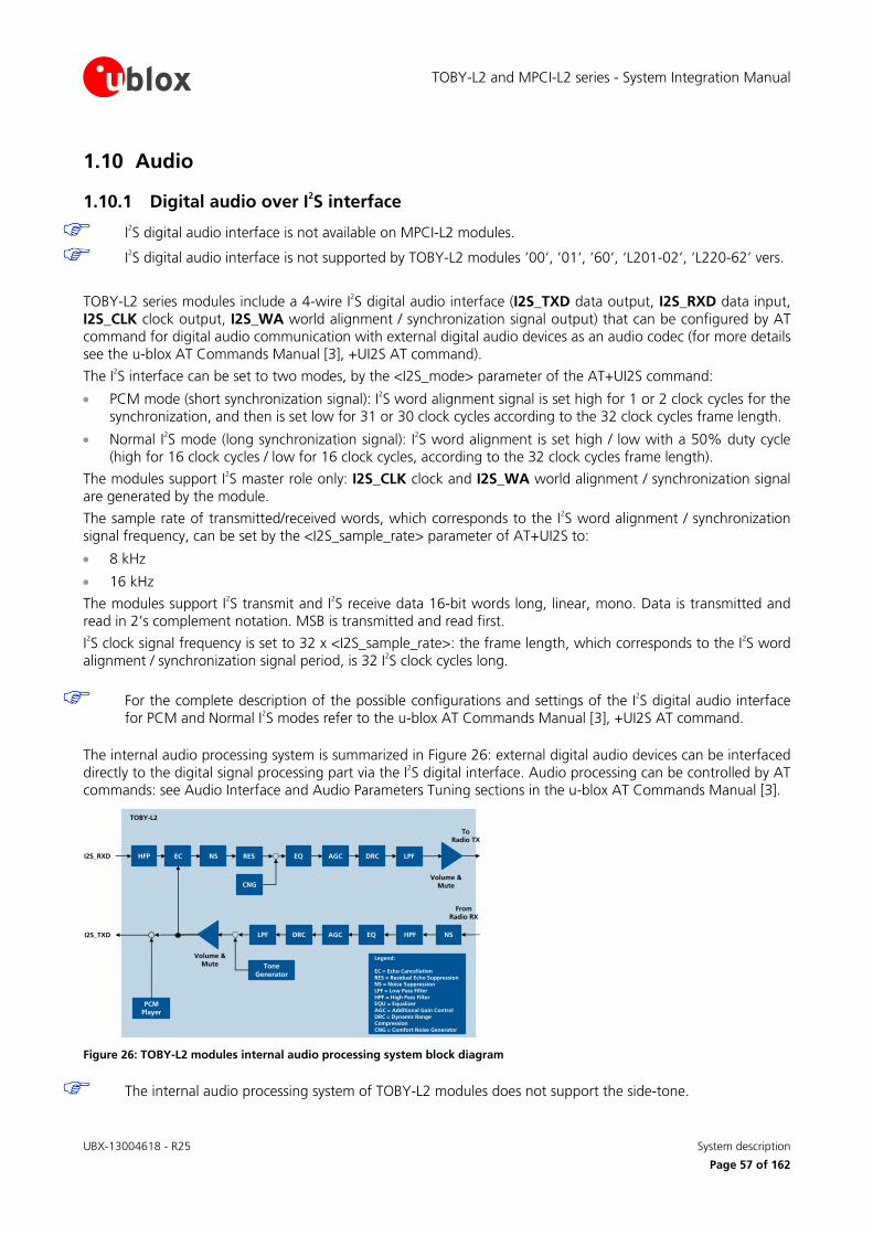
TOBY-L2 and MPCI-L2 series - System Integration Manual
UBX-13004618 - R25 System description
Page 57 of 162
1.10 Audio
1.10.1 Digital audio over I2S interface
I2S digital audio interface is not available on MPCI-L2 modules.
I2S digital audio interface is not supported by TOBY-L2 modules ’00‘, ’01‘, ’60‘, ‘L201-02’, ‘L220-62’ vers.
TOBY-L2 series modules include a 4-wire I2S digital audio interface (I2S_TXD data output, I2S_RXD data input,
I2S_CLK clock output, I2S_WA world alignment / synchronization signal output) that can be configured by AT command for digital audio communication with external digital audio devices as an audio codec (for more details see the u-blox AT Commands Manual [3], +UI2S AT command).
The I2S interface can be set to two modes, by the <I2S_mode> parameter of the AT+UI2S command:
PCM mode (short synchronization signal): I2S word alignment signal is set high for 1 or 2 clock cycles for the
synchronization, and then is set low for 31 or 30 clock cycles according to the 32 clock cycles frame length.
Normal I2S mode (long synchronization signal): I
2S word alignment is set high / low with a 50% duty cycle
(high for 16 clock cycles / low for 16 clock cycles, according to the 32 clock cycles frame length).
The modules support I2S master role only: I2S_CLK clock and I2S_WA world alignment / synchronization signal
are generated by the module.
The sample rate of transmitted/received words, which corresponds to the I2S word alignment / synchronization
signal frequency, can be set by the <I2S_sample_rate> parameter of AT+UI2S to:
8 kHz
16 kHz
The modules support I2S transmit and I
2S receive data 16-bit words long, linear, mono. Data is transmitted and
read in 2’s complement notation. MSB is transmitted and read first.
I2S clock signal frequency is set to 32 x <I2S_sample_rate>: the frame length, which corresponds to the I
2S word
alignment / synchronization signal period, is 32 I2S clock cycles long.
For the complete description of the possible configurations and settings of the I2S digital audio interface
for PCM and Normal I2S modes refer to the u-blox AT Commands Manual [3], +UI2S AT command.
The internal audio processing system is summarized in Figure 26: external digital audio devices can be interfaced directly to the digital signal processing part via the I
2S digital interface. Audio processing can be controlled by AT
commands: see Audio Interface and Audio Parameters Tuning sections in the u-blox AT Commands Manual [3].
ECHFP
To
Radio TX
From
Radio RX
RESNS
DRCLPF EQAGC
I2S_RXD
I2S_TXD
Volume &
Mute
CNG
AGCEQ LPFDRC
NSHPF
Volume &
Mute
PCM
Player
Tone
Generator
Legend:
EC = Echo CancellationRES = Residual Echo SuppressionNS = Noise SuppressionLPF = Low Pass FilterHPF = High Pass FilterEQU = EqualizerAGC = Additional Gain ControlDRC = Dynamic Range CompressionCNG = Comfort Noise Generator
TOBY-L2
Figure 26: TOBY-L2 modules internal audio processing system block diagram
The internal audio processing system of TOBY-L2 modules does not support the side-tone.
TOBY-L2 and MPCI-L2 series - System Integration Manual
UBX-13004618 - R25 System description
Page 58 of 162
1.11 General Purpose Input/Output
GPIOs are not supported by TOBY-L2 modules “00”, “01” and “60” product versions, except for the Wireless Wide Area Network status indication configured on GPIO1 pin.
GPIOs are not available on MPCI-L2 series modules.
TOBY-L2 series modules include 14 pins (GPIO1-GPIO6, I2S_TXD, I2S_RXD, I2S_CLK, I2S_WA, DTR, DSR, DCD, RI) that can be configured as General Purpose Input/Output or to provide custom functions via u-blox AT commands (see the u-blox AT Commands Manual [3], +UGPIOC, +UGPIOR, +UGPIOW AT commands), as summarized in Table 13.
Function Description Default GPIO Configurable GPIOs
Network status indication
Network status: registered home network, registered roaming, data transmission, no service
-- All
SIM card detection SIM card physical presence detection GPIO5 GPIO5
SIM card hot insertion/removal
Enable / disable SIM interface upon detection of external SIM card physical insertion / removal
-- GPIO5
I2S digital audio interface
18 I2S digital audio interface I2S_RXD, I2S_TXD,
I2S_CLK, I2S_WA I2S_RXD, I2S_TXD, I2S_CLK, I2S_WA
Master clock output18
13 MHz / 26 MHz clock output for an external device as an audio codec
GPIO6 GPIO6
Wi-Fi enable Enable/disable the supply of the external u-blox Wi-Fi module connected to the cellular module
GPIO1 All
DSR UART data set ready output DSR DSR
DTR UART data terminal ready input DTR DTR
DCD UART data carrier detect output DCD DCD
RI UART ring indicator output RI RI
General purpose input Input to sense high or low digital level -- All
General purpose output Output to set the high or the low digital level GPIO4 All
Pin disabled Tri-state with an internal active pull-down enabled GPIO2, GPIO3 All
Table 13: TOBY-L2 series GPIO custom functions configuration
18
Not supported by TOBY-L201-02S and TOBY-L220-62S product versions.
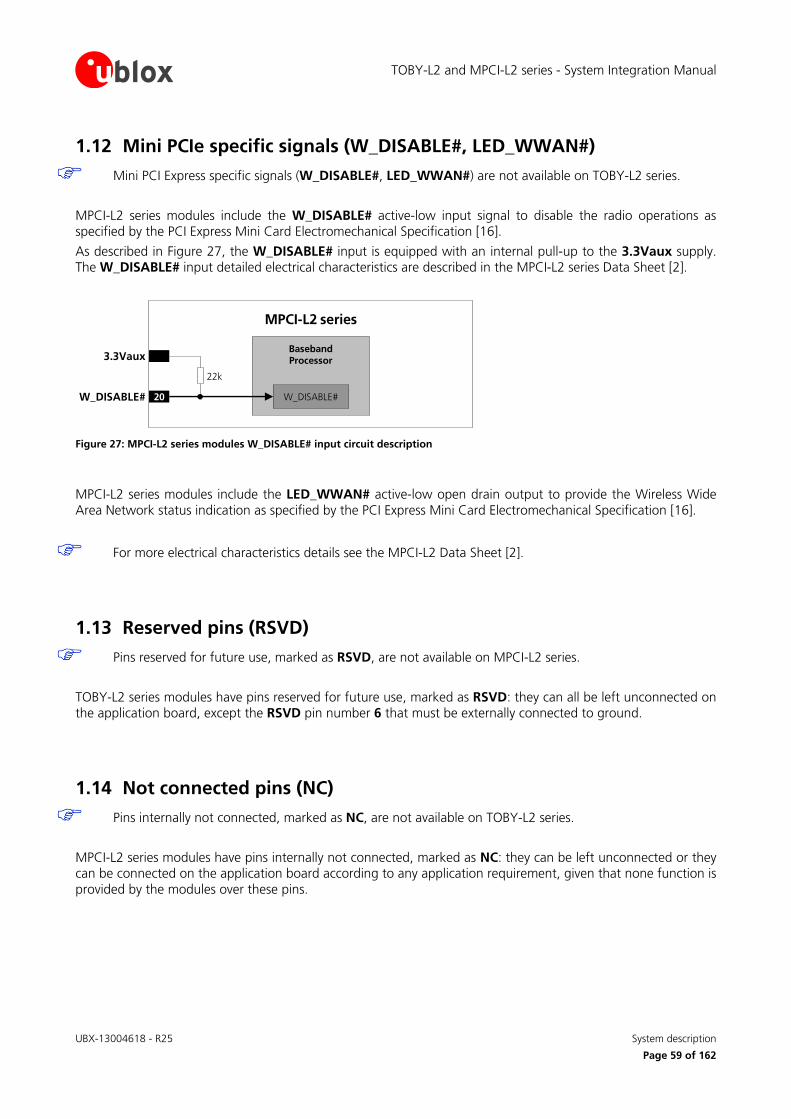
TOBY-L2 and MPCI-L2 series - System Integration Manual
UBX-13004618 - R25 System description
Page 59 of 162
1.12 Mini PCIe specific signals (W_DISABLE#, LED_WWAN#)
Mini PCI Express specific signals (W_DISABLE#, LED_WWAN#) are not available on TOBY-L2 series.
MPCI-L2 series modules include the W_DISABLE# active-low input signal to disable the radio operations as specified by the PCI Express Mini Card Electromechanical Specification [16].
As described in Figure 27, the W_DISABLE# input is equipped with an internal pull-up to the 3.3Vaux supply. The W_DISABLE# input detailed electrical characteristics are described in the MPCI-L2 series Data Sheet [2].
Baseband Processor
20W_DISABLE#
MPCI-L2 series
3.3Vaux
W_DISABLE#
22k
Figure 27: MPCI-L2 series modules W_DISABLE# input circuit description
MPCI-L2 series modules include the LED_WWAN# active-low open drain output to provide the Wireless Wide Area Network status indication as specified by the PCI Express Mini Card Electromechanical Specification [16].
For more electrical characteristics details see the MPCI-L2 Data Sheet [2].
1.13 Reserved pins (RSVD)
Pins reserved for future use, marked as RSVD, are not available on MPCI-L2 series.
TOBY-L2 series modules have pins reserved for future use, marked as RSVD: they can all be left unconnected on the application board, except the RSVD pin number 6 that must be externally connected to ground.
1.14 Not connected pins (NC)
Pins internally not connected, marked as NC, are not available on TOBY-L2 series.
MPCI-L2 series modules have pins internally not connected, marked as NC: they can be left unconnected or they can be connected on the application board according to any application requirement, given that none function is provided by the modules over these pins.
TOBY-L2 and MPCI-L2 series - System Integration Manual
UBX-13004618 - R25 System description
Page 60 of 162
1.15 System features
1.15.1 Network indication
MPCI-L2 series modules include the LED_WWAN# active-low open drain output to provide the Wireless Wide Area Network status indication as per PCI Express Mini Card Electromechanical Specification [16].
GPIOs are not supported by TOBY-L2 modules “00”, “01”, “60” product versions, but the Wireless Wide Area Network status indication is by default configured on the GPIO1 pin.
The GPIO1 can be configured by the AT+UGPIOC command (for further details see the u-blox AT Commands Manual [3]), to indicate network status as described below:
No service (no network coverage or not registered)
Registered 2G / 3G / LTE home network
Registered 2G / 3G / LTE visitor network (roaming)
Call enabled (RF data transmission / reception)
1.15.2 Antenna supervisor
Antenna supervisor (i.e. antenna detection) is not available on MPCI-L2 series.
Antenna supervisor (i.e. antenna detection) is not supported by TOBY-L2 series modules “00”, “01” and “60” product versions.
The antenna detection function provided by the ANT_DET pin is based on an ADC measurement as optional feature that can be implemented if the application requires it. The antenna supervisor is forced by the +UANTR AT command (see the u-blox AT Commands Manual [3] for more details).
The requirements to achieve antenna detection functionality are the following:
an RF antenna assembly with a built-in resistor (diagnostic circuit) must be used
an antenna detection circuit must be implemented on the application board
See section 1.7.2 for detailed antenna detection interface functional description and see section 2.4.2 for detection circuit on application board and diagnostic circuit on antenna assembly design-in guidelines.
1.15.3 Jamming detection
Congestion detection (i.e. jamming detection) is not supported by “00”, “01”, “02” “03”, “60” and “62” product versions.
In real network situations modules can experience various kind of out-of-coverage conditions: limited service conditions when roaming to networks not supporting the specific SIM, limited service in cells which are not suitable or barred due to operators’ choices, no cell condition when moving to poorly served or highly interfered areas. In the latter case, interference can be artificially injected in the environment by a noise generator covering a given spectrum, thus obscuring the operator’s carriers entitled to give access to the LTE/3G/2G service.
The congestion (i.e. jamming) detection feature can be enabled and configured by the +UCD AT command: the feature consists of detecting an anomalous source of interference and signaling the start and stop of such conditions to the host application processor with an unsolicited indication, which can react appropriately by e.g. switching off the radio transceiver of the module (i.e. configuring the module in “airplane mode” by means of the +CFUN AT command) in order to reduce power consumption and monitoring the environment at constant periods (for more details see the u-blox AT Commands Manual [3]).
TOBY-L2 and MPCI-L2 series - System Integration Manual
UBX-13004618 - R25 System description
Page 61 of 162
1.15.4 IP modes of operation
IP modes of operation refer to the TOBY-L2 and MPCI-L2 series modules configuration related to the network IP termination and network interfaces settings in general. IP modes of operation are the following:
Bridge mode: In bridge mode the module acts as a cellular modem dongle connected to the host over serial interface. The IP termination of the network is placed on the host IP stack. The module is configured as a bridge which means the network IP address is assigned to the host (host IP termination).
Router mode: In router mode the module acts as a cellular modem router which means the IP termination of the network is placed on the internal IP stack of the module (on-target IP termination). In particular, in this configuration the application processor belongs to a private network and is not aware of the mobile connectivity setup of the module.
For more details about IP modes of operation see the u-blox AT Commands Manual [3].
1.15.5 Dual stack IPv4/IPv6
TOBY-L2 and MPCI-L2 series support both Internet Protocol version 4 and Internet Protocol version 6 in parallel.
For more details about dual stack IPv4/IPv6 see the u-blox AT Commands Manual [3].
1.15.6 TCP/IP and UDP/IP
Embedded TCP/IP and UDP/IP stack as well as Direct Link mode are not supported by the “00” and “60” product versions.
TOBY-L2 and MPCI-L2 series modules provide embedded TCP/IP and UDP/IP protocol stack: a PDP context can be configured, established and handled via the data connection management packet switched data commands.
TOBY-L2 and MPCI-L2 series modules provide Direct Link mode to establish a transparent end-to-end communication with an already connected TCP or UDP socket via serial interfaces (USB, UART). In Direct Link mode, data sent to the serial interface from an external application processor is forwarded to the network and vice-versa.
For more details about embedded TCP/IP and UDP/IP functionalities see the u-blox AT Commands Manual [3].
1.15.7 FTP
Embedded FTP services as well as Direct Link mode are not supported by “00” and “60” product versions.
TOBY-L2 and MPCI-L2 series provide embedded File Transfer Protocol (FTP) services. Files are read and stored in the local file system of the module.
FTP files can also be transferred using FTP Direct Link:
FTP download: data coming from the FTP server is forwarded to the host processor via USB / UART serial interfaces (for FTP without Direct Link mode the data is always stored in the module’s Flash File System)
FTP upload: data coming from the host processor via USB / UART serial interface is forwarded to the FTP server (for FTP without Direct Link mode the data is read from the module’s Flash File System)
When Direct Link is used for a FTP file transfer, only the file content pass through USB / UART serial interface, whereas all the FTP commands handling is managed internally by the FTP application.
For more details about embedded FTP functionalities see u-blox AT Commands Manual [3].
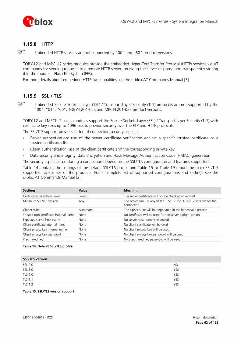
TOBY-L2 and MPCI-L2 series - System Integration Manual
UBX-13004618 - R25 System description
Page 62 of 162
1.15.8 HTTP
Embedded HTTP services are not supported by “00” and “60” product versions.
TOBY-L2 and MPCI-L2 series modules provide the embedded Hyper-Text Transfer Protocol (HTTP) services via AT commands for sending requests to a remote HTTP server, receiving the server response and transparently storing it in the module’s Flash File System (FFS).
For more details about embedded HTTP functionalities see the u-blox AT Commands Manual [3].
1.15.9 SSL / TLS
Embedded Secure Sockets Layer (SSL) / Transport Layer Security (TLS) protocols are not supported by the “00”, “01”, “60”, TOBY-L201-02S and MPCI-L201-02S product versions.
TOBY-L2 and MPCI-L2 series modules support the Secure Sockets Layer (SSL) / Transport Layer Security (TLS) with certificate key sizes up to 4096 bits to provide security over the FTP and HTTP protocols.
The SSL/TLS support provides different connection security aspects:
Server authentication: use of the server certificate verification against a specific trusted certificate or a trusted certificates list
Client authentication: use of the client certificate and the corresponding private key
Data security and integrity: data encryption and Hash Message Authentication Code (HMAC) generation
The security aspects used during a connection depend on the SSL/TLS configuration and features supported.
Table 14 contains the settings of the default SSL/TLS profile and Table 15 to Table 19 report the main SSL/TLS supported capabilities of the products. For a complete list of supported configurations and settings see the u-blox AT Commands Manual [3].
Settings Value Meaning
Certificates validation level Level 0 The server certificate will not be checked or verified
Minimum SSL/TLS version Any The server can use any of the TLS1.0/TLS1.1/TLS1.2 versions for the connection
Cipher suite Automatic The cipher suite will be negotiated in the handshake process
Trusted root certificate internal name None No certificate will be used for the server authentication
Expected server host-name None No server host-name is expected
Client certificate internal name None No client certificate will be used
Client private key internal name None No client private key will be used
Client private key password None No client private key password will be used
Pre-shared key None No pre-shared key password will be used
Table 14: Default SSL/TLS profile
SSL/TLS Version
SSL 2.0 NO
SSL 3.0 YES
TLS 1.0 YES
TLS 1.1 YES
TLS 1.2 YES
Table 15: SSL/TLS version support
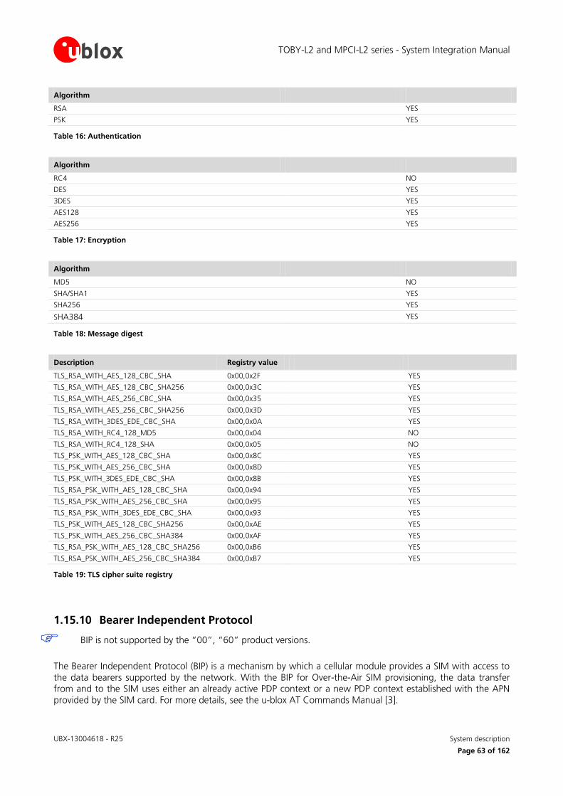
TOBY-L2 and MPCI-L2 series - System Integration Manual
UBX-13004618 - R25 System description
Page 63 of 162
Algorithm
RSA YES
PSK YES
Table 16: Authentication
Algorithm
RC4 NO
DES YES
3DES YES
AES128 YES
AES256 YES
Table 17: Encryption
Algorithm
MD5 NO
SHA/SHA1 YES
SHA256 YES
SHA384 YES
Table 18: Message digest
Description Registry value
TLS_RSA_WITH_AES_128_CBC_SHA 0x00,0x2F YES
TLS_RSA_WITH_AES_128_CBC_SHA256 0x00,0x3C YES
TLS_RSA_WITH_AES_256_CBC_SHA 0x00,0x35 YES
TLS_RSA_WITH_AES_256_CBC_SHA256 0x00,0x3D YES
TLS_RSA_WITH_3DES_EDE_CBC_SHA 0x00,0x0A YES
TLS_RSA_WITH_RC4_128_MD5 0x00,0x04 NO
TLS_RSA_WITH_RC4_128_SHA 0x00,0x05 NO
TLS_PSK_WITH_AES_128_CBC_SHA 0x00,0x8C YES
TLS_PSK_WITH_AES_256_CBC_SHA 0x00,0x8D YES
TLS_PSK_WITH_3DES_EDE_CBC_SHA 0x00,0x8B YES
TLS_RSA_PSK_WITH_AES_128_CBC_SHA 0x00,0x94 YES
TLS_RSA_PSK_WITH_AES_256_CBC_SHA 0x00,0x95 YES
TLS_RSA_PSK_WITH_3DES_EDE_CBC_SHA 0x00,0x93 YES
TLS_PSK_WITH_AES_128_CBC_SHA256 0x00,0xAE YES
TLS_PSK_WITH_AES_256_CBC_SHA384 0x00,0xAF YES
TLS_RSA_PSK_WITH_AES_128_CBC_SHA256 0x00,0xB6 YES
TLS_RSA_PSK_WITH_AES_256_CBC_SHA384 0x00,0xB7 YES
Table 19: TLS cipher suite registry
1.15.10 Bearer Independent Protocol
BIP is not supported by the “00”, “60” product versions.
The Bearer Independent Protocol (BIP) is a mechanism by which a cellular module provides a SIM with access to the data bearers supported by the network. With the BIP for Over-the-Air SIM provisioning, the data transfer from and to the SIM uses either an already active PDP context or a new PDP context established with the APN provided by the SIM card. For more details, see the u-blox AT Commands Manual [3].
TOBY-L2 and MPCI-L2 series - System Integration Manual
UBX-13004618 - R25 System description
Page 64 of 162
1.15.11 Wi-Fi integration
u-blox short range communication Wi-Fi modules integration is not available for MPCI-L2 series modules.
u-blox short range communication Wi-Fi modules integration is not supported by the TOBY-L2 series modules “00”, “01” and “60” product versions.
Full access to u-blox short range communication Wi-Fi modules is available through a dedicated SDIO interface (see sections 1.9.4 and 2.6.4). This means that combining a TOBY-L2 series cellular module with a u-blox short range communication module gives designers full access to the Wi-Fi module directly via the cellular module, so that a second interface connected to the Wi-Fi module is not necessary.
AT commands via the AT interfaces of the cellular module (UART, USB) allows a full control of the Wi-Fi module from any host processor, because Wi-Fi control messages are relayed to the Wi-Fi module via the dedicated SDIO interface (for more details, see the Wi-Fi AT commands in the u-blox AT Commands Manual [3]).
All the management software for Wi-Fi module operations runs inside the cellular module in addition to those required for cellular-only operation: Wi-Fi driver, Web User Interface (WebUI), Connection Config Manager.
For more details, see the Wi-Fi / Cellular Integration Application Note [15].
1.15.12 Firmware update Over AT (FOAT)
This feature allows upgrading the module firmware over USB / UART serial interfaces, using AT commands.
The +UFWUPD AT command triggers a reboot followed by the upgrade procedure at specified a baud rate
A special boot loader on the module performs firmware installation, security verifications and module reboot
Firmware authenticity verification is performed via a security signature during the download. The firmware is then installed, overwriting the current version. In case of power loss during this phase, the boot loader detects a fault at the next wake-up, and restarts the firmware download. After completing the upgrade, the module is reset again and wakes-up in normal boot
For more details about Firmware update Over AT procedure see the Firmware Update Application Note [6] and the u-blox AT Commands Manual [3], +UFWUPD AT command.
1.15.13 Firmware update Over The Air (FOTA)
Firmware update Over The Air (FOTA) is not supported by “00” and “60” product versions.
This feature allows upgrading the module firmware over the LTE/3G/2G air interface.
In order to reduce the amount of data to be transmitted over the air, the implemented FOTA feature requires downloading only a “delta file” instead of the full firmware. The delta file contains only the differences between the two firmware versions (old and new), and is compressed. The firmware update procedure can be triggered using dedicated AT command with the delta file stored in the module file system via over the air FTP.
For more details about Firmware update Over The Air procedure see the Firmware Update Application Note [6] and the u-blox AT Commands Manual [3], +UFWINSTALL AT command.
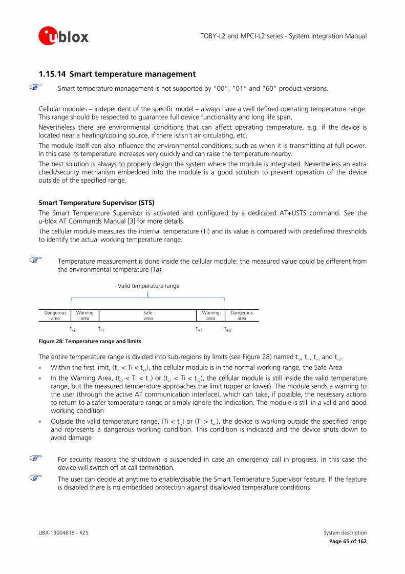
TOBY-L2 and MPCI-L2 series - System Integration Manual
UBX-13004618 - R25 System description
Page 65 of 162
1.15.14 Smart temperature management
Smart temperature management is not supported by “00”, “01” and “60” product versions.
Cellular modules – independent of the specific model – always have a well defined operating temperature range. This range should be respected to guarantee full device functionality and long life span.
Nevertheless there are environmental conditions that can affect operating temperature, e.g. if the device is located near a heating/cooling source, if there is/isn’t air circulating, etc.
The module itself can also influence the environmental conditions; such as when it is transmitting at full power. In this case its temperature increases very quickly and can raise the temperature nearby.
The best solution is always to properly design the system where the module is integrated. Nevertheless an extra check/security mechanism embedded into the module is a good solution to prevent operation of the device outside of the specified range.
Smart Temperature Supervisor (STS)
The Smart Temperature Supervisor is activated and configured by a dedicated AT+USTS command. See the u-blox AT Commands Manual [3] for more details.
The cellular module measures the internal temperature (Ti) and its value is compared with predefined thresholds to identify the actual working temperature range.
Temperature measurement is done inside the cellular module: the measured value could be different from the environmental temperature (Ta).
Warningarea
t-1 t+1 t+2t-2
Valid temperature range
Safearea
Dangerousarea
Dangerousarea
Warningarea
Figure 28: Temperature range and limits
The entire temperature range is divided into sub-regions by limits (see Figure 28) named t-2, t
-1, t
+1 and t
+2.
Within the first limit, (t-1 < Ti < t
+1), the cellular module is in the normal working range, the Safe Area
In the Warning Area, (t-2 < Ti < t
.1) or (t
+1 < Ti < t
+2), the cellular module is still inside the valid temperature
range, but the measured temperature approaches the limit (upper or lower). The module sends a warning to the user (through the active AT communication interface), which can take, if possible, the necessary actions to return to a safer temperature range or simply ignore the indication. The module is still in a valid and good working condition
Outside the valid temperature range, (Ti < t-2) or (Ti > t
+2), the device is working outside the specified range
and represents a dangerous working condition. This condition is indicated and the device shuts down to avoid damage
For security reasons the shutdown is suspended in case an emergency call in progress. In this case the device will switch off at call termination.
The user can decide at anytime to enable/disable the Smart Temperature Supervisor feature. If the feature is disabled there is no embedded protection against disallowed temperature conditions.
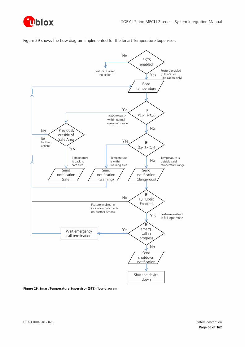
TOBY-L2 and MPCI-L2 series - System Integration Manual
UBX-13004618 - R25 System description
Page 66 of 162
Figure 29 shows the flow diagram implemented for the Smart Temperature Supervisor.
IF STS
enabled
Read
temperature
IF
(t-1<Ti<t+1)
IF
(t-2<Ti<t+2)
Send
notification
(warning)
Send
notification
(dangerous)
Wait emergency
call termination
IF
emerg.
call in
progress
Shut the device
down
Yes
No
Yes
Yes
No
No
No
Yes
Send
shutdown
notification
Feature enabled
(full logic or
indication only)
IF
Full Logic
Enabled
Feature disabled:
no action
Temperature is
within normal
operating range
Yes
Tempetature
is within
warning area
Tempetature is
outside valid
temperature range
No
Featuere enabled
in full logic mode
Feature enabled in
indication only mode:
no further actions
Send
notification
(safe)
Previously
outside of
Safe Area
Tempetature
is back to
safe area
No
No
further
actions
Yes
Figure 29: Smart Temperature Supervisor (STS) flow diagram
TOBY-L2 and MPCI-L2 series - System Integration Manual
UBX-13004618 - R25 System description
Page 67 of 162
Threshold Definitions
When the application of cellular module operates at extreme temperatures with Smart Temperature Supervisor enabled, the user should note that outside the valid temperature range the device will automatically shut down as described above.
The input for the algorithm is always the temperature measured within the cellular module (Ti, internal). This value can be higher than the working ambient temperature (Ta, ambient), as (for example) during transmission at maximum power a significant fraction of DC input power is dissipated as heat This behavior is partially compensated by the definition of the upper shutdown threshold (t
+2) that is slightly higher than the declared
environmental temperature limit.
The temperature thresholds are defined according the Table 20.
Symbol Parameter Temperature Remarks
t-2 Low temperature shutdown –40 °C
Equal to the absolute minimum temperature rating for the wireless module (the lower limit of the extended temperature range)
t-1 Low temperature warning –30 °C 10°C above t
-2
t+1
High temperature warning +77 °C
20°C below t+2
. The higher warning area for upper range ensures that any countermeasures used to limit the thermal heating will become
effective, even considering some thermal inertia of the complete assembly.
t+2
High temperature shutdown +97 °C*
Equal to the internal temperature Ti measured in the worst case operating condition at typical supply voltage when the ambient temperature Ta in the reference setup** equals the absolute maximum
temperature rating (upper limit of the extended temperature range)
* +90 °C for TOBY-L201-02S and MPCI-L201-02S product versions
** Module mounted on a 79 mm x 62 mm x 1.46 mm 4-Layers PCB with a high coverage of copper within climatic chamber
Table 20: Thresholds definition for Smart Temperature Supervisor
The sensor measures board temperature inside the shields, which can differ from ambient temperature.
1.15.15 SIM Access Profile (SAP)
Not supported by “00”, “01”, “02”, “60” and “62” product versions.
SIM access profile (SAP) feature allows cellular modules to access and use a remote (U)SIM card instead of the local SIM card directly connected to the module (U)SIM interface.
The modules provide a dedicated USB SAP channel for communication with the remote (U)SIM card.
The communication between u-blox cellular modules and the remote SIM is conformed to client-server paradigm: the module is the SAP client establishing a connection and performing data exchange to an SAP server directly connected to the remote SIM that is used by the module for cellular network operations. The SAP communication protocol is based on the SIM Access Profile Interoperability Specification [29].
u-blox cellular modules do not support SAP server role: the module acts as SAP client only.
A typical application using the SAP feature is the scenario where a device such as an embedded car-phone with an integrated TOBY-L2 module uses a remote SIM included in an external user device (e.g. a simple SIM card reader or a portable phone), which is brought into the car. The car-phone accesses the cellular network using the remote SIM in the external device.
u-blox cellular modules, acting as an SAP client, can be connected to an SAP server by a completely wired connection, as shown in Figure 30.
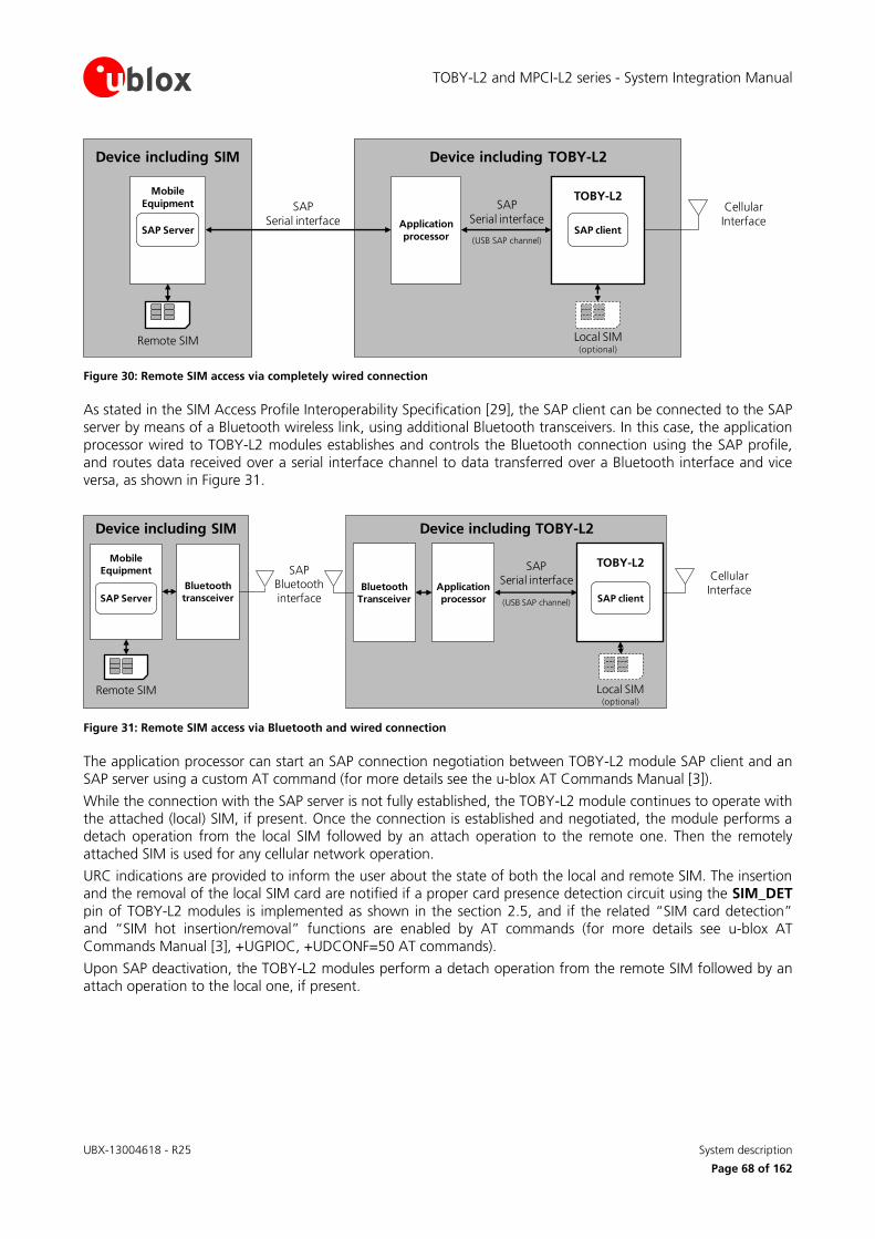
TOBY-L2 and MPCI-L2 series - System Integration Manual
UBX-13004618 - R25 System description
Page 68 of 162
Device including TOBY-L2
Cellular Interface
SAP Serial interface
(USB SAP channel)
Local SIM(optional)
TOBY-L2
SAP clientApplication
processor
Device including SIM
SAP Serial interface
Remote SIM
Mobile
Equipment
SAP Server
Figure 30: Remote SIM access via completely wired connection
As stated in the SIM Access Profile Interoperability Specification [29], the SAP client can be connected to the SAP server by means of a Bluetooth wireless link, using additional Bluetooth transceivers. In this case, the application processor wired to TOBY-L2 modules establishes and controls the Bluetooth connection using the SAP profile, and routes data received over a serial interface channel to data transferred over a Bluetooth interface and vice versa, as shown in Figure 31.
Device including TOBY-L2
SAP Serial interface
(USB SAP channel)
Cellular Interface
Local SIM(optional)
TOBY-L2
SAP clientApplication
processor
SAP Bluetooth interface
Bluetooth
Transceiver
Device including SIM
Remote SIM
Mobile
Equipment
SAP Server
Bluetooth
transceiver
Figure 31: Remote SIM access via Bluetooth and wired connection
The application processor can start an SAP connection negotiation between TOBY-L2 module SAP client and an SAP server using a custom AT command (for more details see the u-blox AT Commands Manual [3]).
While the connection with the SAP server is not fully established, the TOBY-L2 module continues to operate with the attached (local) SIM, if present. Once the connection is established and negotiated, the module performs a detach operation from the local SIM followed by an attach operation to the remote one. Then the remotely attached SIM is used for any cellular network operation.
URC indications are provided to inform the user about the state of both the local and remote SIM. The insertion and the removal of the local SIM card are notified if a proper card presence detection circuit using the SIM_DET pin of TOBY-L2 modules is implemented as shown in the section 2.5, and if the related “SIM card detection” and “SIM hot insertion/removal” functions are enabled by AT commands (for more details see u-blox AT Commands Manual [3], +UGPIOC, +UDCONF=50 AT commands).
Upon SAP deactivation, the TOBY-L2 modules perform a detach operation from the remote SIM followed by an attach operation to the local one, if present.
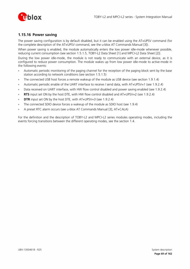
TOBY-L2 and MPCI-L2 series - System Integration Manual
UBX-13004618 - R25 System description
Page 69 of 162
1.15.16 Power saving
The power saving configuration is by default disabled, but it can be enabled using the AT+UPSV command (for the complete description of the AT+UPSV command, see the u-blox AT Commands Manual [3]).
When power saving is enabled, the module automatically enters the low power idle-mode whenever possible, reducing current consumption (see section 1.5.1.5, TOBY-L2 Data Sheet [1] and MPCI-L2 Data Sheet [2]).
During the low power idle-mode, the module is not ready to communicate with an external device, as it is configured to reduce power consumption. The module wakes up from low power idle-mode to active-mode in the following events:
Automatic periodic monitoring of the paging channel for the reception of the paging block sent by the base station according to network conditions (see section 1.5.1.5)
The connected USB host forces a remote wakeup of the module as USB device (see section 1.9.1.4)
Automatic periodic enable of the UART interface to receive / send data, with AT+UPSV=1 (see 1.9.2.4)
Data received on UART interface, with HW flow control disabled and power saving enabled (see 1.9.2.4)
RTS input set ON by the host DTE, with HW flow control disabled and AT+UPSV=2 (see 1.9.2.4)
DTR input set ON by the host DTE, with AT+UPSV=3 (see 1.9.2.4)
The connected SDIO device forces a wakeup of the module as SDIO host (see 1.9.4)
A preset RTC alarm occurs (see u-blox AT Commands Manual [3], AT+CALA)
For the definition and the description of TOBY-L2 and MPCI-L2 series modules operating modes, including the events forcing transitions between the different operating modes, see the section 1.4.
TOBY-L2 and MPCI-L2 series - System Integration Manual
UBX-13004618 - R25 Design-in
Page 70 of 162
2 Design-in
2.1 Overview
For an optimal integration of TOBY-L2 and MPCI-L2 series modules in the final application board follow the design guidelines stated in this section.
Every application circuit must be properly designed to guarantee the correct functionality of the relative interface, however a number of points require high attention during the design of the application device.
The following list provides a rank of importance in the application design, starting from the highest relevance:
1. Module antenna connection: ANT1, ANT2 and ANT_DET.
Antenna circuit directly affects the RF compliance of the device integrating a TOBY-L2 and MPCI-L2 series module with applicable certification schemes. Very carefully follow the suggestions provided in the relative section 2.4 for schematic and layout design.
2. Module supply: VCC or 3.3Vaux and GND pins.
The supply circuit affects the RF compliance of the device integrating a TOBY-L2 and MPCI-L2 series module with applicable required certification schemes as well as antenna circuit design. Very carefully follow the suggestions provided in the relative section 2.2.1 for schematic and layout design.
3. USB interface: USB_D+, USB_D- pins.
Accurate design is required to guarantee USB 2.0 high-speed interface functionality. Carefully follow the suggestions provided in the relative section 2.6.1 for schematic and layout design.
4. SIM interface: VSIM, SIM_CLK, SIM_IO, SIM_RST or UIM_PWR, UIM_DATA, UIM_CLK, UIM_RESET pins.
Accurate design is required to guarantee SIM card functionality reducing the risk of RF coupling. Carefully follow the suggestions provided in the relative section 2.5 for schematic and layout design.
5. SDIO interface: SDIO_D0, SDIO_D1, SDIO_D2, SDIO_D3, SDIO_CLK, SDIO_CMD pins.
Accurate design is required to guarantee SDIO interface functionality. Carefully follow the suggestions provided in the relative section 2.6.4 for schematic and layout design.
6. System functions: RESET_N or PERST#, PWR_ON pins.
Accurate design is required to guarantee that the voltage level is well defined during operation. Carefully follow the suggestions provided in the relative section 2.3 for schematic and layout design.
7. Other supplies: V_BCKP RTC supply and V_INT generic digital interfaces supply.
Accurate design is required to guarantee proper functionality. Follow the suggestions provided in the corresponding sections 2.2.2 and 2.2.3 for schematic and layout design.
8. Other digital interfaces: UART, I2C, I
2S, Host Select, GPIOs, Mini PCIe specific signals and Reserved pins.
Accurate design is required to guarantee proper functionality. Follow the suggestions provided in sections 2.6.2, 2.6.3, 2.7.1, 2.3.3, 2.8, 2.9 and 2.10 for schematic and layout design.
TOBY-L2 and MPCI-L2 series - System Integration Manual
UBX-13004618 - R25 Design-in
Page 71 of 162
2.2 Supply interfaces
2.2.1 Module supply (VCC or 3.3Vaux)
2.2.1.1 General guidelines for VCC or 3.3Vaux supply circuit selection and design
VCC or 3.3Vaux pins are internally connected. Application design shall connect all the available pads to the external supply to minimize the power loss due to series resistance.
GND pins are internally connected. Application design shall connect all the available pads to solid ground on the application board, since a good (low impedance) connection to external ground can minimize power loss and improve RF and thermal performance.
TOBY-L2 and MPCI-L2 series modules must be sourced through the VCC or the 3.3Vaux pins with a proper DC power supply that should meet the following prerequisites to comply with the modules’ VCC or 3.3Vaux requirements summarized in Table 7.
The proper DC power supply can be selected according to the application requirements (see Figure 32) between the different possible supply sources types, which most common ones are the following:
Switching regulator
Low Drop-Out (LDO) linear regulator
Rechargeable Lithium-ion (Li-Ion) or Lithium-ion polymer (Li-Pol) battery, for TOBY-L2 series only
Primary (disposable) battery, for TOBY-L2 series only
Main Supply
Available?
Battery
Li-Ion 3.7 V
Linear LDO
RegulatorMain Supply
Voltage > 5V?
Switching Step-Down Regulator
No, portable device
No, less than 5 V
Yes, greater than 5 V
Yes, always available
Figure 32: VCC supply concept selection
The switching step-down regulator is the typical choice when the available primary supply source has a nominal voltage much higher (e.g. greater than 5 V) than the operating supply voltage of TOBY-L2 and MPCI-L2 series. The use of switching step-down provides the best power efficiency for the overall application and minimizes current drawn from the main supply source. See 2.2.1.2, 2.2.1.6, 2.2.1.9, 2.2.1.10 for specific design-in.
The use of an LDO linear regulator becomes convenient for a primary supply with a relatively low voltage (e.g. less or equal than 5 V). In this case the typical 90% efficiency of the switching regulator diminishes the benefit of voltage step-down and no true advantage is gained in input current savings. On the opposite side, linear regulators are not recommended for high voltage step-down as they dissipate a considerable amount of energy in thermal power. See 2.2.1.3, 2.2.1.6, 2.2.1.9, 2.2.1.10 for specific design-in.
If TOBY-L2 modules are deployed in a mobile unit where no permanent primary supply source is available, then a battery will be required to provide VCC. A standard 3-cell Li-Ion or Li-Pol battery pack directly connected to VCC is the usual choice for battery-powered devices. During charging, batteries with Ni-MH chemistry typically reach a maximum voltage that is above the maximum rating for VCC, and should therefore be avoided. See 2.2.1.4, 2.2.1.6, 2.2.1.9, 2.2.1.10 for specific design-in.
Keep in mind that the use of rechargeable batteries requires the implementation of a suitable charger circuit which is not included in the modules. The charger circuit has to be designed to prevent over-voltage on VCC pins of the module, and it should be selected according to the application requirements: a DC/DC switching
TOBY-L2 and MPCI-L2 series - System Integration Manual
UBX-13004618 - R25 Design-in
Page 72 of 162
charger is the typical choice when the charging source has an high nominal voltage (e.g. ~12 V), whereas a linear charger is the typical choice when the charging source has a relatively low nominal voltage (~5 V). If both a permanent primary supply / charging source (e.g. ~12 V) and a rechargeable back-up battery (e.g. 3.7 V Li-Pol) are available at the same time in the application as possible supply source, then a proper charger / regulator with integrated power path management function can be selected to supply the module while simultaneously and independently charging the battery. See 2.2.1.7, 2.2.1.8 and 2.2.1.6, 2.2.1.9, 2.2.1.10 for specific design-in.
The use of a primary (not rechargeable) battery is in general uncommon, but appropriate parts can be selected given that the most cells available are seldom capable of delivering the maximum current specified in TOBY-L2 series Data Sheet [1] during connected-mode. Carefully evaluate the usage of super-capacitors as supply source since aging and temperature conditions significantly affect the actual capacitor characteristics. See 2.2.1.5 and 2.2.1.6, 2.2.1.9, 2.2.1.10 for specific design-in.
Rechargeable 3-cell Li-Ion or Li-Pol and Ni-MH chemistry batteries reach a maximum voltage that is above the maximum rating for the 3.3Vaux supply of MPCI-L2 modules, and should therefore be avoided. The use of rechargeable, not-rechargeable battery or super-capacitors is very uncommon for Mini PCI Express applications, so that these supply sources types are not considered for MPCI-L2 modules.
The usage of more than one DC supply at the same time should be carefully evaluated: depending on the supply source characteristics, different DC supply systems can result as mutually exclusive.
The following sections highlight some design aspects for each of the supplies listed above providing application circuit design-in compliant with the module VCC requirements summarized in Table 7.
2.2.1.2 Guidelines for VCC or 3.3Vaux supply circuit design using a switching regulator
The use of a switching regulator is suggested when the difference from the available supply rail to the VCC or the 3.3Vaux value is high, since switching regulators provide good efficiency transforming a 12 V or greater voltage supply to the typical 3.8 V value of the VCC supply or the typical 3.3 V value of the 3.3Vaux supply.
The characteristics of the switching regulator connected to VCC or 3.3Vaux pins should meet the following prerequisites to comply with the module VCC or 3.3Vaux requirements summarized in Table 7:
Power capability: the switching regulator with its output circuit must be capable of providing a voltage value to the VCC or 3.3Vaux pins within the specified operating range and must be capable of delivering to VCC or 3.3Vaux pins the maximum peak / pulse current consumption during Tx burst at maximum Tx power specified in the TOBY-L2 series Data Sheet [1] or in the MPCI-L2 series Data Sheet [2].
Low output ripple: the switching regulator together with its output circuit must be capable of providing a clean (low noise) VCC or 3.3Vaux voltage profile.
High switching frequency: for best performance and for smaller applications it is recommended to select a switching frequency ≥ 600 kHz (since L-C output filter is typically smaller for high switching frequency). The use of a switching regulator with a variable switching frequency or with a switching frequency lower than 600 kHz must be carefully evaluated since this can produce noise in the VCC or 3.3Vaux voltage profile and therefore negatively impact LTE/3G/2G modulation spectrum performance. An additional L-C low-pass filter between the switching regulator output to VCC or 3.3Vaux supply pins can mitigate the ripple at the input of the module, but adds extra voltage drop due to resistive losses on series inductors.
PWM mode operation: it is preferable to select regulators with Pulse Width Modulation (PWM) mode. While in connected-mode, the Pulse Frequency Modulation (PFM) mode and PFM/PWM modes transitions must be avoided to reduce the noise on the VCC or 3.3Vaux voltage profile. Switching regulators can be used that are able to switch between low ripple PWM mode and high ripple PFM mode, provided that the mode transition occurs when the module changes status from the idle/active-modes to connected-mode. It is permissible to use a regulator that switches from the PWM mode to the burst or PFM mode at an appropriate current threshold.
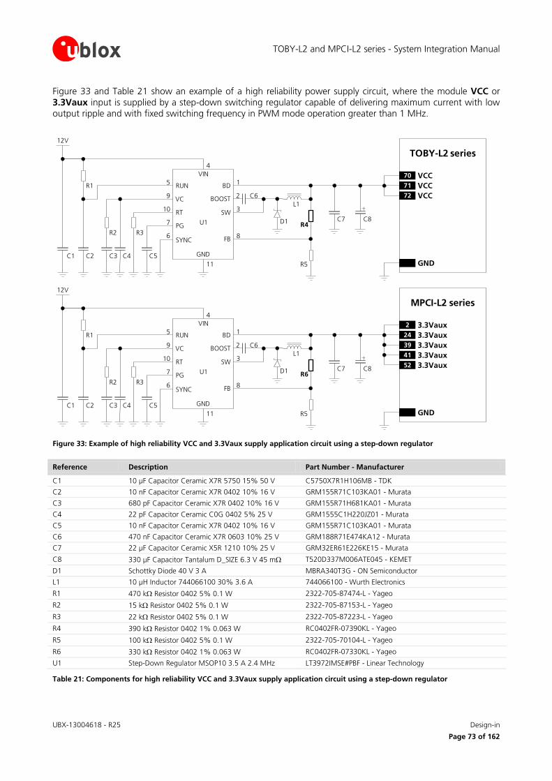
TOBY-L2 and MPCI-L2 series - System Integration Manual
UBX-13004618 - R25 Design-in
Page 73 of 162
Figure 33 and Table 21 show an example of a high reliability power supply circuit, where the module VCC or 3.3Vaux input is supplied by a step-down switching regulator capable of delivering maximum current with low output ripple and with fixed switching frequency in PWM mode operation greater than 1 MHz.
12V
C5
R3
C4
R2
C2C1
R1
VIN
RUN
VC
RT
PG
SYNC
BD
BOOST
SW
FB
GND
6
7
10
9
5
C6
1
2
3
8
11
4
C7 C8D1R4
R5
L1
C3
U1
TOBY-L2 series
71 VCC
72 VCC
70 VCC
GND
12V
C5
R3
C4
R2
C2C1
R1
VIN
RUN
VC
RT
PG
SYNC
BD
BOOST
SW
FB
GND
6
7
10
9
5
C6
1
2
3
8
11
4
C7 C8D1R6
R5
L1
C3
U1
MPCI-L2 series
24 3.3Vaux
39 3.3Vaux
2 3.3Vaux
GND
41 3.3Vaux
52 3.3Vaux
Figure 33: Example of high reliability VCC and 3.3Vaux supply application circuit using a step-down regulator
Reference Description Part Number - Manufacturer
C1 10 µF Capacitor Ceramic X7R 5750 15% 50 V C5750X7R1H106MB - TDK
C2 10 nF Capacitor Ceramic X7R 0402 10% 16 V GRM155R71C103KA01 - Murata
C3 680 pF Capacitor Ceramic X7R 0402 10% 16 V GRM155R71H681KA01 - Murata
C4 22 pF Capacitor Ceramic C0G 0402 5% 25 V GRM1555C1H220JZ01 - Murata
C5 10 nF Capacitor Ceramic X7R 0402 10% 16 V GRM155R71C103KA01 - Murata
C6 470 nF Capacitor Ceramic X7R 0603 10% 25 V GRM188R71E474KA12 - Murata
C7 22 µF Capacitor Ceramic X5R 1210 10% 25 V GRM32ER61E226KE15 - Murata
C8 330 µF Capacitor Tantalum D_SIZE 6.3 V 45 m T520D337M006ATE045 - KEMET
D1 Schottky Diode 40 V 3 A MBRA340T3G - ON Semiconductor
L1 10 µH Inductor 744066100 30% 3.6 A 744066100 - Wurth Electronics
R1 470 k Resistor 0402 5% 0.1 W 2322-705-87474-L - Yageo
R2 15 k Resistor 0402 5% 0.1 W 2322-705-87153-L - Yageo
R3 22 k Resistor 0402 5% 0.1 W 2322-705-87223-L - Yageo
R4 390 k Resistor 0402 1% 0.063 W RC0402FR-07390KL - Yageo
R5 100 k Resistor 0402 5% 0.1 W 2322-705-70104-L - Yageo
R6 330 k Resistor 0402 1% 0.063 W RC0402FR-07330KL - Yageo
U1 Step-Down Regulator MSOP10 3.5 A 2.4 MHz LT3972IMSE#PBF - Linear Technology
Table 21: Components for high reliability VCC and 3.3Vaux supply application circuit using a step-down regulator
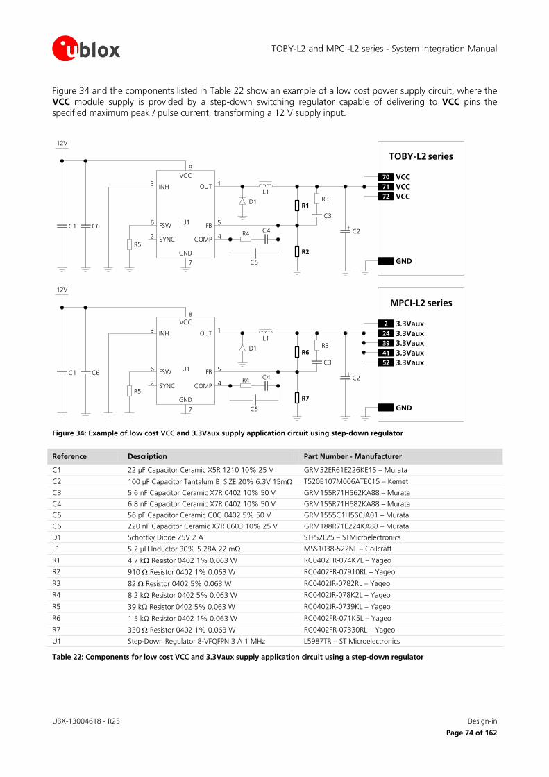
TOBY-L2 and MPCI-L2 series - System Integration Manual
UBX-13004618 - R25 Design-in
Page 74 of 162
Figure 34 and the components listed in Table 22 show an example of a low cost power supply circuit, where the VCC module supply is provided by a step-down switching regulator capable of delivering to VCC pins the specified maximum peak / pulse current, transforming a 12 V supply input.
TOBY-L2 series
12V
R5
C6C1
VCC
INH
FSW
SYNC
OUT
GND
2
6
3 1
7
8
C3
C2
D1R1
R2
L1
U1
GND
FB
COMP
5
4
R3
C4R4
C5
71 VCC
72 VCC
70 VCC
12V
R5
C6C1
VCC
INH
FSW
SYNC
OUT
GND
2
6
3 1
7
8
C3
C2
D1R6
R7
L1
U1
GND
FB
COMP
5
4
R3
C4R4
C5
MPCI-L2 series
24 3.3Vaux
39 3.3Vaux
2 3.3Vaux
41 3.3Vaux
52 3.3Vaux
Figure 34: Example of low cost VCC and 3.3Vaux supply application circuit using step-down regulator
Reference Description Part Number - Manufacturer
C1 22 µF Capacitor Ceramic X5R 1210 10% 25 V GRM32ER61E226KE15 – Murata
C2 100 µF Capacitor Tantalum B_SIZE 20% 6.3V 15m T520B107M006ATE015 – Kemet
C3 5.6 nF Capacitor Ceramic X7R 0402 10% 50 V GRM155R71H562KA88 – Murata
C4 6.8 nF Capacitor Ceramic X7R 0402 10% 50 V GRM155R71H682KA88 – Murata
C5 56 pF Capacitor Ceramic C0G 0402 5% 50 V GRM1555C1H560JA01 – Murata
C6 220 nF Capacitor Ceramic X7R 0603 10% 25 V GRM188R71E224KA88 – Murata
D1 Schottky Diode 25V 2 A STPS2L25 – STMicroelectronics
L1 5.2 µH Inductor 30% 5.28A 22 m MSS1038-522NL – Coilcraft
R1 4.7 k Resistor 0402 1% 0.063 W RC0402FR-074K7L – Yageo
R2 910 Resistor 0402 1% 0.063 W RC0402FR-07910RL – Yageo
R3 82 Resistor 0402 5% 0.063 W RC0402JR-0782RL – Yageo
R4 8.2 k Resistor 0402 5% 0.063 W RC0402JR-078K2L – Yageo
R5 39 k Resistor 0402 5% 0.063 W RC0402JR-0739KL – Yageo
R6 1.5 k Resistor 0402 1% 0.063 W RC0402FR-071K5L – Yageo
R7 330 Resistor 0402 1% 0.063 W RC0402FR-07330RL – Yageo
U1 Step-Down Regulator 8-VFQFPN 3 A 1 MHz L5987TR – ST Microelectronics
Table 22: Components for low cost VCC and 3.3Vaux supply application circuit using a step-down regulator
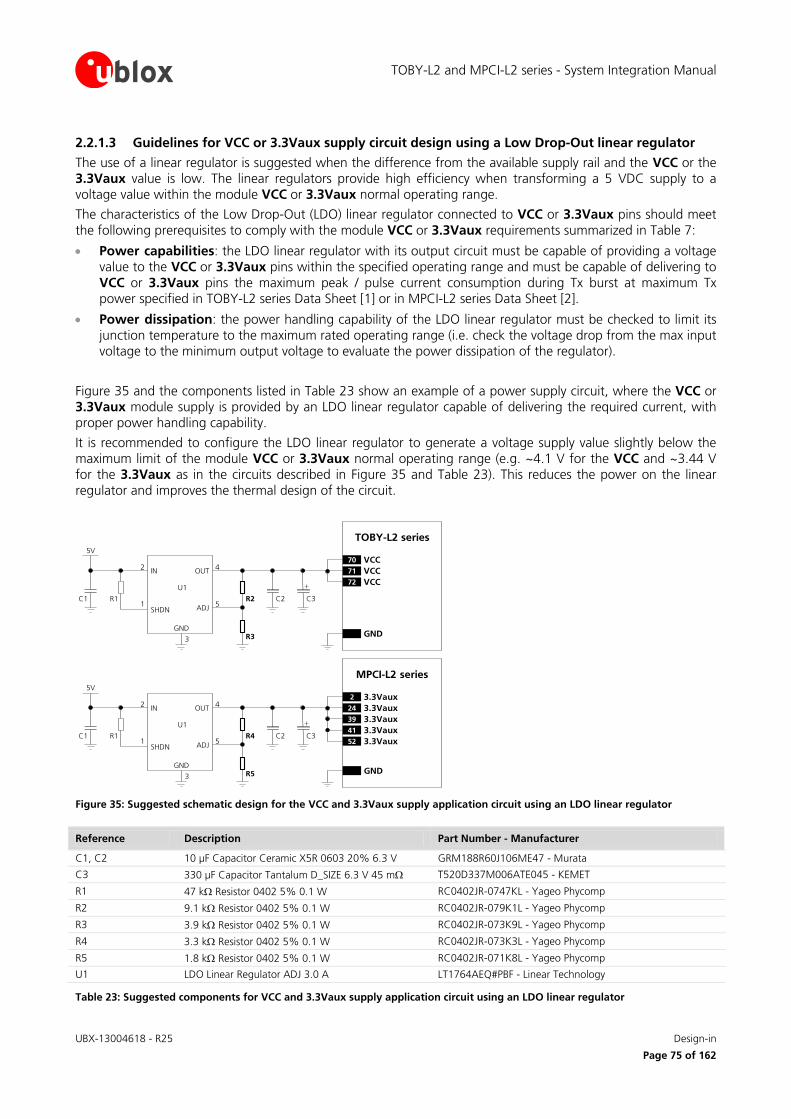
TOBY-L2 and MPCI-L2 series - System Integration Manual
UBX-13004618 - R25 Design-in
Page 75 of 162
2.2.1.3 Guidelines for VCC or 3.3Vaux supply circuit design using a Low Drop-Out linear regulator
The use of a linear regulator is suggested when the difference from the available supply rail and the VCC or the 3.3Vaux value is low. The linear regulators provide high efficiency when transforming a 5 VDC supply to a voltage value within the module VCC or 3.3Vaux normal operating range.
The characteristics of the Low Drop-Out (LDO) linear regulator connected to VCC or 3.3Vaux pins should meet the following prerequisites to comply with the module VCC or 3.3Vaux requirements summarized in Table 7:
Power capabilities: the LDO linear regulator with its output circuit must be capable of providing a voltage value to the VCC or 3.3Vaux pins within the specified operating range and must be capable of delivering to VCC or 3.3Vaux pins the maximum peak / pulse current consumption during Tx burst at maximum Tx power specified in TOBY-L2 series Data Sheet [1] or in MPCI-L2 series Data Sheet [2].
Power dissipation: the power handling capability of the LDO linear regulator must be checked to limit its junction temperature to the maximum rated operating range (i.e. check the voltage drop from the max input voltage to the minimum output voltage to evaluate the power dissipation of the regulator).
Figure 35 and the components listed in Table 23 show an example of a power supply circuit, where the VCC or 3.3Vaux module supply is provided by an LDO linear regulator capable of delivering the required current, with proper power handling capability.
It is recommended to configure the LDO linear regulator to generate a voltage supply value slightly below the maximum limit of the module VCC or 3.3Vaux normal operating range (e.g. ~4.1 V for the VCC and ~3.44 V for the 3.3Vaux as in the circuits described in Figure 35 and Table 23). This reduces the power on the linear regulator and improves the thermal design of the circuit.
5V
C1 R1
IN OUT
ADJ
GND
1
2 4
5
3
C2R2
R3
U1
SHDN
TOBY-L2 series
71 VCC
72 VCC
70 VCC
GND
C3
5V
C1 R1
IN OUT
ADJ
GND
1
2 4
5
3
C2R4
R5
U1
SHDN
MPCI-L2 series
GND
C3
24 3.3Vaux
39 3.3Vaux
2 3.3Vaux
41 3.3Vaux
52 3.3Vaux
Figure 35: Suggested schematic design for the VCC and 3.3Vaux supply application circuit using an LDO linear regulator
Reference Description Part Number - Manufacturer
C1, C2 10 µF Capacitor Ceramic X5R 0603 20% 6.3 V GRM188R60J106ME47 - Murata
C3 330 µF Capacitor Tantalum D_SIZE 6.3 V 45 m T520D337M006ATE045 - KEMET
R1 47 k Resistor 0402 5% 0.1 W RC0402JR-0747KL - Yageo Phycomp
R2 9.1 k Resistor 0402 5% 0.1 W RC0402JR-079K1L - Yageo Phycomp
R3 3.9 k Resistor 0402 5% 0.1 W RC0402JR-073K9L - Yageo Phycomp
R4 3.3 k Resistor 0402 5% 0.1 W RC0402JR-073K3L - Yageo Phycomp
R5 1.8 k Resistor 0402 5% 0.1 W RC0402JR-071K8L - Yageo Phycomp
U1 LDO Linear Regulator ADJ 3.0 A LT1764AEQ#PBF - Linear Technology
Table 23: Suggested components for VCC and 3.3Vaux supply application circuit using an LDO linear regulator
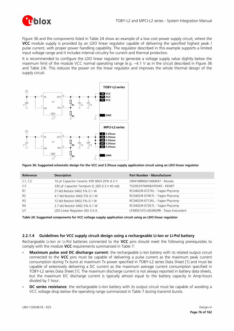
TOBY-L2 and MPCI-L2 series - System Integration Manual
UBX-13004618 - R25 Design-in
Page 76 of 162
Figure 36 and the components listed in Table 24 show an example of a low cost power supply circuit, where the VCC module supply is provided by an LDO linear regulator capable of delivering the specified highest peak / pulse current, with proper power handling capability. The regulator described in this example supports a limited input voltage range and it includes internal circuitry for current and thermal protection.
It is recommended to configure the LDO linear regulator to generate a voltage supply value slightly below the maximum limit of the module VCC normal operating range (e.g. ~4.1 V as in the circuit described in Figure 36 and Table 24). This reduces the power on the linear regulator and improves the whole thermal design of the supply circuit.
5V
C1
IN OUT
ADJ
GND
1
2 4
5
3
C2R1
R2
U1
EN
TOBY-L2 series
71 VCC
72 VCC
70 VCC
GND
C3
5V
C1
IN OUT
ADJ
GND
1
2 4
5
3
C2R3
R4
U1
EN
MPCI-L2 series
GND
C3
24 3.3Vaux
39 3.3Vaux
2 3.3Vaux
41 3.3Vaux
52 3.3Vaux
Figure 36: Suggested schematic design for the VCC and 3.3Vaux supply application circuit using an LDO linear regulator
Reference Description Part Number - Manufacturer
C1, C2 10 µF Capacitor Ceramic X5R 0603 20% 6.3 V GRM188R60J106ME47 - Murata
C3 330 µF Capacitor Tantalum D_SIZE 6.3 V 45 m T520D337M006ATE045 - KEMET
R1 27 k Resistor 0402 5% 0.1 W RC0402JR-0727KL - Yageo Phycomp
R2 4.7 k Resistor 0402 5% 0.1 W RC0402JR-074K7L - Yageo Phycomp
R3 12 k Resistor 0402 5% 0.1 W RC0402JR-0712KL - Yageo Phycomp
R4 2.7 k Resistor 0402 5% 0.1 W RC0402JR-072K7L - Yageo Phycomp
U1 LDO Linear Regulator ADJ 3.0 A LP38501ATJ-ADJ/NOPB - Texas Instrument
Table 24: Suggested components for VCC voltage supply application circuit using an LDO linear regulator
2.2.1.4 Guidelines for VCC supply circuit design using a rechargeable Li-Ion or Li-Pol battery
Rechargeable Li-Ion or Li-Pol batteries connected to the VCC pins should meet the following prerequisites to comply with the module VCC requirements summarized in Table 7:
Maximum pulse and DC discharge current: the rechargeable Li-Ion battery with its related output circuit connected to the VCC pins must be capable of delivering a pulse current as the maximum peak current consumption during Tx burst at maximum Tx power specified in TOBY-L2 series Data Sheet [1] and must be capable of extensively delivering a DC current as the maximum average current consumption specified in TOBY-L2 series Data Sheet [1]. The maximum discharge current is not always reported in battery data sheets, but the maximum DC discharge current is typically almost equal to the battery capacity in Amp-hours divided by 1 hour.
DC series resistance: the rechargeable Li-Ion battery with its output circuit must be capable of avoiding a VCC voltage drop below the operating range summarized in Table 7 during transmit bursts.
TOBY-L2 and MPCI-L2 series - System Integration Manual
UBX-13004618 - R25 Design-in
Page 77 of 162
2.2.1.5 Guidelines for VCC supply circuit design using a primary (disposable) battery
The characteristics of a primary (non-rechargeable) battery connected to VCC pins should meet the following prerequisites to comply with the module VCC requirements summarized in Table 7:
Maximum pulse and DC discharge current: the non-rechargeable battery with its related output circuit connected to the VCC pins must be capable of delivering a pulse current as the maximum peak current consumption during Tx burst at maximum Tx power specified in TOBY-L2 series Data Sheet [1] and must be capable of extensively delivering a DC current as the maximum average current consumption specified in TOBY-L2 series Data Sheet [1]. The maximum discharge current is not always reported in battery data sheets, but the maximum DC discharge current is typically almost equal to the battery capacity in Amp-hours divided by 1 hour.
DC series resistance: the non-rechargeable battery with its output circuit must be capable of avoiding a VCC voltage drop below the operating range summarized in Table 7 during transmit bursts.
2.2.1.6 Additional guidelines for VCC or 3.3Vaux supply circuit design
To reduce voltage drops, use a low impedance power source. The series resistance of the power supply lines (connected to the modules’ VCC / 3.3Vaux and GND pins) on the application board and battery pack should also be considered and minimized: cabling and routing must be as short as possible to minimize power losses.
Three pins are allocated to VCC supply and five pins to 3.3Vaux supply. Several pins are designated for GND connection. Even if all the VCC / 3.3Vaux pins and all the GND pins are internally connected within the module, it is recommended to properly connect all of them to supply the module to minimize series resistance losses.
To avoid voltage drop undershoot and overshoot at the start and end of a transmit burst during a GSM call (when current consumption on the VCC or 3.3Vaux supply can rise up as specified in TOBY-L2 series Data Sheet [1] or in MPCI-L2 series Data Sheet [2]), place a bypass capacitor with large capacitance (at least 100 µF) and low ESR near the VCC pins, for example:
330 µF capacitance, 45 m ESR (e.g. KEMET T520D337M006ATE045, Tantalum Capacitor)
To reduce voltage ripple and noise, improving RF performance especially if the application device integrates an internal antenna, place the following bypass capacitors near the VCC / 3.3Vaux pins:
68 pF capacitor with Self-Resonant Frequency in the 800/900 MHz range (e.g. Murata GRM1555C1H680J) to filter EMI in the RF low frequencies bands
15 pF capacitor with Self-Resonant Frequency in 1800/1900 MHz range (e.g. Murata GRM1555C1E150J) to filter EMI in the RF high frequencies bands
8.2 pF capacitor with Self-Resonant Frequency in 2500/2600 MHz range (e.g. Murata GRM1555C1H8R2D) to filter EMI in the RF very high frequencies band
10 nF capacitor (e.g. Murata GRM155R71C103K) to filter digital logic noise from clocks and data sources
100 nF capacitor (e.g. Murata GRM155R61C104K) to filter digital logic noise from clocks and data sources
A suitable series ferrite bead can be properly placed on the VCC / 3.3Vaux line for additional noise filtering if required by the specific application according to the whole application board design.
The necessity of each part depends on the specific design, but it is recommended to provide all the bypass capacitors described in Figure 37 / Table 25 if the application device integrates an internal antenna.
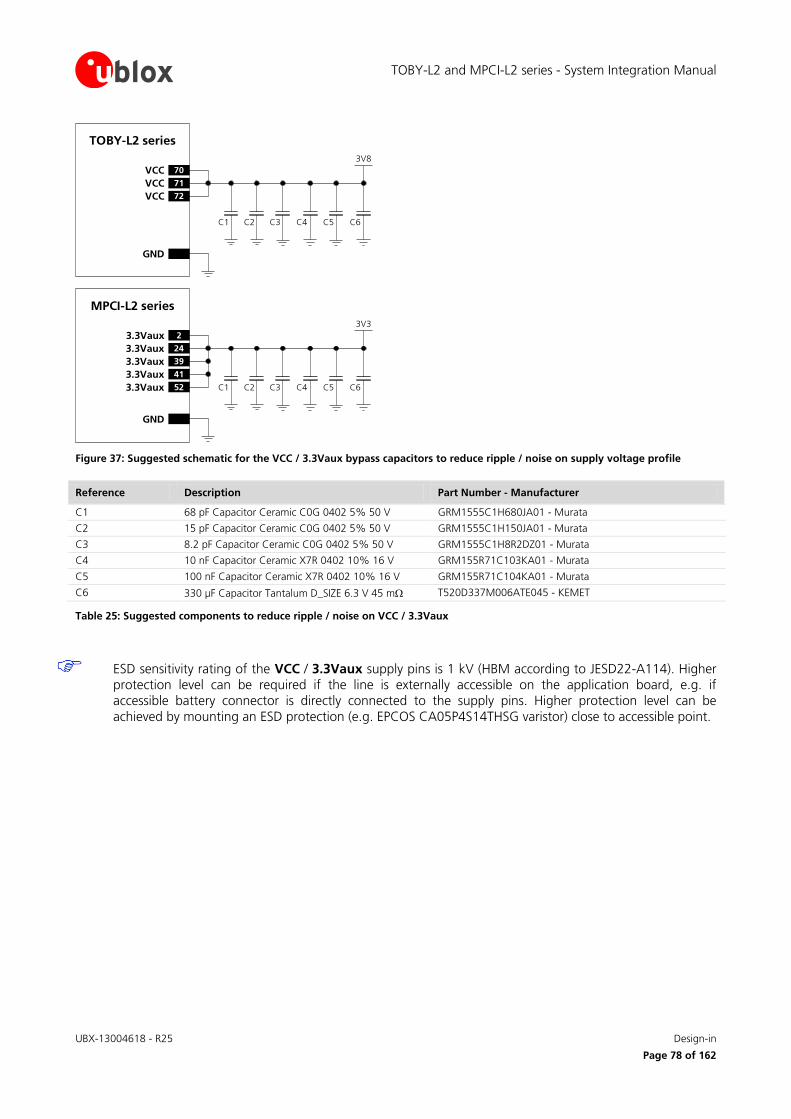
TOBY-L2 and MPCI-L2 series - System Integration Manual
UBX-13004618 - R25 Design-in
Page 78 of 162
C2
GND
C3 C4
TOBY-L2 series
71VCC
72VCC
70VCC
C1 C5 C6
3V8
C2
GND
C3 C4
MPCI-L2 series
C1 C5 C6
3V3
243.3Vaux
393.3Vaux
23.3Vaux
413.3Vaux
523.3Vaux
Figure 37: Suggested schematic for the VCC / 3.3Vaux bypass capacitors to reduce ripple / noise on supply voltage profile
Reference Description Part Number - Manufacturer
C1 68 pF Capacitor Ceramic C0G 0402 5% 50 V GRM1555C1H680JA01 - Murata
C2 15 pF Capacitor Ceramic C0G 0402 5% 50 V GRM1555C1H150JA01 - Murata
C3 8.2 pF Capacitor Ceramic C0G 0402 5% 50 V GRM1555C1H8R2DZ01 - Murata
C4 10 nF Capacitor Ceramic X7R 0402 10% 16 V GRM155R71C103KA01 - Murata
C5 100 nF Capacitor Ceramic X7R 0402 10% 16 V GRM155R71C104KA01 - Murata
C6 330 µF Capacitor Tantalum D_SIZE 6.3 V 45 m T520D337M006ATE045 - KEMET
Table 25: Suggested components to reduce ripple / noise on VCC / 3.3Vaux
ESD sensitivity rating of the VCC / 3.3Vaux supply pins is 1 kV (HBM according to JESD22-A114). Higher protection level can be required if the line is externally accessible on the application board, e.g. if accessible battery connector is directly connected to the supply pins. Higher protection level can be achieved by mounting an ESD protection (e.g. EPCOS CA05P4S14THSG varistor) close to accessible point.
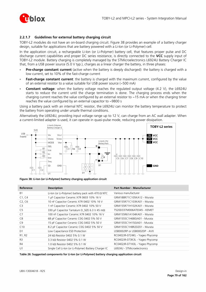
TOBY-L2 and MPCI-L2 series - System Integration Manual
UBX-13004618 - R25 Design-in
Page 79 of 162
2.2.1.7 Guidelines for external battery charging circuit
TOBY-L2 modules do not have an on-board charging circuit. Figure 38 provides an example of a battery charger design, suitable for applications that are battery powered with a Li-Ion (or Li-Polymer) cell.
In the application circuit, a rechargeable Li-Ion (or Li-Polymer) battery cell, that features proper pulse and DC discharge current capabilities and proper DC series resistance, is directly connected to the VCC supply input of TOBY-L2 module. Battery charging is completely managed by the STMicroelectronics L6924U Battery Charger IC that, from a USB power source (5.0 V typ.), charges as a linear charger the battery, in three phases:
Pre-charge constant current (active when the battery is deeply discharged): the battery is charged with a low current, set to 10% of the fast-charge current
Fast-charge constant current: the battery is charged with the maximum current, configured by the value of an external resistor to a value suitable for USB power source (~500 mA)
Constant voltage: when the battery voltage reaches the regulated output voltage (4.2 V), the L6924U starts to reduce the current until the charge termination is done. The charging process ends when the charging current reaches the value configured by an external resistor to ~15 mA or when the charging timer reaches the value configured by an external capacitor to ~9800 s
Using a battery pack with an internal NTC resistor, the L6924U can monitor the battery temperature to protect the battery from operating under unsafe thermal conditions.
Alternatively the L6924U, providing input voltage range up to 12 V, can charge from an AC wall adapter. When a current-limited adapter is used, it can operate in quasi-pulse mode, reducing power dissipation.
C5 C8C7C6 C9
GND
TOBY-L2 series
71 VCC
72 VCC
70 VCC
+
USB
Supply
C3 R4
θ
U1
IUSB
IAC
IEND
TPRG
SD
VIN
VINSNS
MODE
ISEL
C2C1
5V0
TH
GND
VOUT
VOSNS
VREF
R1
R2
R3
Li-Ion/Li-Pol Battery Pack
D1
B1
C4
Li-Ion/Li-Polymer Battery Charger IC
C10
Figure 38: Li-Ion (or Li-Polymer) battery charging application circuit
Reference Description Part Number - Manufacturer
B1 Li-Ion (or Li-Polymer) battery pack with 470 NTC Various manufacturer
C1, C4 1 µF Capacitor Ceramic X7R 0603 10% 16 V GRM188R71C105KA12 - Murata
C2, C6 10 nF Capacitor Ceramic X7R 0402 10% 16 V GRM155R71C103KA01 - Murata
C3 1 nF Capacitor Ceramic X7R 0402 10% 50 V GRM155R71H102KA01 - Murata
C5 330 µF Capacitor Tantalum D_SIZE 6.3 V 45 m T520D337M006ATE045 - KEMET
C7 100 nF Capacitor Ceramic X7R 0402 10% 16 V GRM155R61A104KA01 - Murata
C8 68 pF Capacitor Ceramic C0G 0402 5% 50 V GRM1555C1H680JA01 - Murata
C9 15 pF Capacitor Ceramic C0G 0402 5% 50 V GRM1555C1H150JA01 - Murata
C10 8.2 pF Capacitor Ceramic C0G 0402 5% 50 V GRM1555C1H8R2DZ01 - Murata
D1 Low Capacitance ESD Protection USB0002RP or USB0002DP - AVX
R1, R2 24 k Resistor 0402 5% 0.1 W RC0402JR-0724KL - Yageo Phycomp
R3 3.3 k Resistor 0402 5% 0.1 W RC0402JR-073K3L - Yageo Phycomp
R4 1.0 k Resistor 0402 5% 0.1 W RC0402JR-071K0L - Yageo Phycomp
U1 Single Cell Li-Ion (or Li-Polymer) Battery Charger IC L6924U - STMicroelectronics
Table 26: Suggested components for Li-Ion (or Li-Polymer) battery charging application circuit
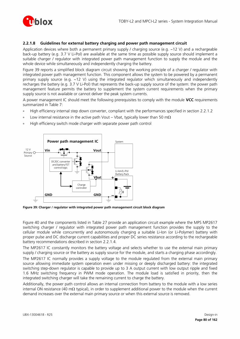
TOBY-L2 and MPCI-L2 series - System Integration Manual
UBX-13004618 - R25 Design-in
Page 80 of 162
2.2.1.8 Guidelines for external battery charging and power path management circuit
Application devices where both a permanent primary supply / charging source (e.g. ~12 V) and a rechargeable back-up battery (e.g. 3.7 V Li-Pol) are available at the same time as possible supply source should implement a suitable charger / regulator with integrated power path management function to supply the module and the whole device while simultaneously and independently charging the battery.
Figure 39 reports a simplified block diagram circuit showing the working principle of a charger / regulator with integrated power path management function. This component allows the system to be powered by a permanent primary supply source (e.g. ~12 V) using the integrated regulator which simultaneously and independently recharges the battery (e.g. 3.7 V Li-Pol) that represents the back-up supply source of the system: the power path management feature permits the battery to supplement the system current requirements when the primary supply source is not available or cannot deliver the peak system currents.
A power management IC should meet the following prerequisites to comply with the module VCC requirements summarized in Table 7:
High efficiency internal step down converter, compliant with the performances specified in section 2.2.1.2
Low internal resistance in the active path Vout – Vbat, typically lower than 50 m
High efficiency switch mode charger with separate power path control
GND
Power path management IC
VoutVin
θ
Li-Ion/Li-Pol Battery Pack
GND
System
12 V
Primary Source
Charge controller
DC/DC converter
and battery FET control logic
Vbat
Figure 39: Charger / regulator with integrated power path management circuit block diagram
Figure 40 and the components listed in Table 27 provide an application circuit example where the MPS MP2617 switching charger / regulator with integrated power path management function provides the supply to the cellular module while concurrently and autonomously charging a suitable Li-Ion (or Li-Polymer) battery with proper pulse and DC discharge current capabilities and proper DC series resistance according to the rechargeable battery recommendations described in section 2.2.1.4.
The MP2617 IC constantly monitors the battery voltage and selects whether to use the external main primary supply / charging source or the battery as supply source for the module, and starts a charging phase accordingly.
The MP2617 IC normally provides a supply voltage to the module regulated from the external main primary source allowing immediate system operation even under missing or deeply discharged battery: the integrated switching step-down regulator is capable to provide up to 3 A output current with low output ripple and fixed 1.6 MHz switching frequency in PWM mode operation. The module load is satisfied in priority, then the integrated switching charger will take the remaining current to charge the battery.
Additionally, the power path control allows an internal connection from battery to the module with a low series
internal ON resistance (40 m typical), in order to supplement additional power to the module when the current demand increases over the external main primary source or when this external source is removed.
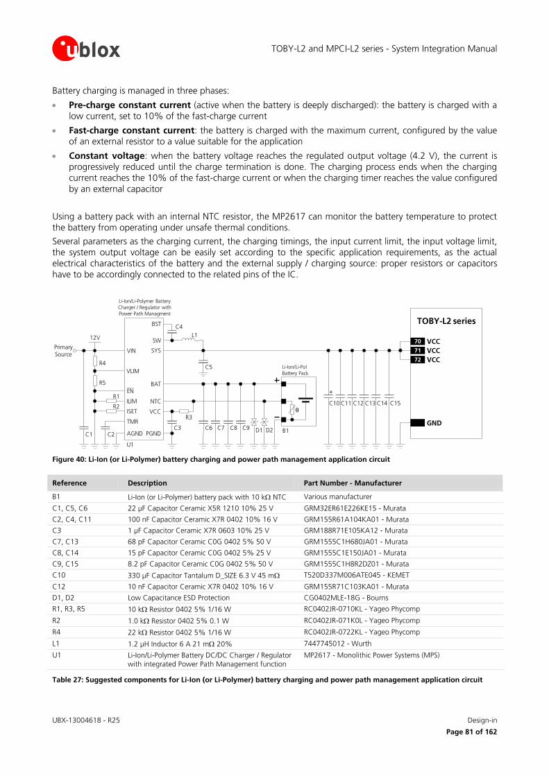
TOBY-L2 and MPCI-L2 series - System Integration Manual
UBX-13004618 - R25 Design-in
Page 81 of 162
Battery charging is managed in three phases:
Pre-charge constant current (active when the battery is deeply discharged): the battery is charged with a low current, set to 10% of the fast-charge current
Fast-charge constant current: the battery is charged with the maximum current, configured by the value of an external resistor to a value suitable for the application
Constant voltage: when the battery voltage reaches the regulated output voltage (4.2 V), the current is progressively reduced until the charge termination is done. The charging process ends when the charging current reaches the 10% of the fast-charge current or when the charging timer reaches the value configured by an external capacitor
Using a battery pack with an internal NTC resistor, the MP2617 can monitor the battery temperature to protect the battery from operating under unsafe thermal conditions.
Several parameters as the charging current, the charging timings, the input current limit, the input voltage limit, the system output voltage can be easily set according to the specific application requirements, as the actual electrical characteristics of the battery and the external supply / charging source: proper resistors or capacitors have to be accordingly connected to the related pins of the IC.
C10 C13
GND
C12C11 C14
TOBY-L2 series
71 VCC
72 VCC
70 VCC
+
Primary Source
R3
U1
EN
ILIM
ISET
TMR
AGND
VIN
C2C1
12V
NTC
PGND
SW
SYS
BAT
C4
R1
R2
D1
θ
Li-Ion/Li-Pol
Battery Pack
B1
C5
Li-Ion/Li-Polymer Battery
Charger / Regulator with
Power Path Managment
VCC
C3 C6
L1
BST
D2
VLIM
R4
R5
C7 C8 C9
C15
Figure 40: Li-Ion (or Li-Polymer) battery charging and power path management application circuit
Reference Description Part Number - Manufacturer
B1 Li-Ion (or Li-Polymer) battery pack with 10 k NTC Various manufacturer
C1, C5, C6 22 µF Capacitor Ceramic X5R 1210 10% 25 V GRM32ER61E226KE15 - Murata
C2, C4, C11 100 nF Capacitor Ceramic X7R 0402 10% 16 V GRM155R61A104KA01 - Murata
C3 1 µF Capacitor Ceramic X7R 0603 10% 25 V GRM188R71E105KA12 - Murata
C7, C13 68 pF Capacitor Ceramic C0G 0402 5% 50 V GRM1555C1H680JA01 - Murata
C8, C14 15 pF Capacitor Ceramic C0G 0402 5% 25 V GRM1555C1E150JA01 - Murata
C9, C15 8.2 pF Capacitor Ceramic C0G 0402 5% 50 V GRM1555C1H8R2DZ01 - Murata
C10 330 µF Capacitor Tantalum D_SIZE 6.3 V 45 m T520D337M006ATE045 - KEMET
C12 10 nF Capacitor Ceramic X7R 0402 10% 16 V GRM155R71C103KA01 - Murata
D1, D2 Low Capacitance ESD Protection CG0402MLE-18G - Bourns
R1, R3, R5 10 k Resistor 0402 5% 1/16 W RC0402JR-0710KL - Yageo Phycomp
R2 1.0 k Resistor 0402 5% 0.1 W RC0402JR-071K0L - Yageo Phycomp
R4 22 k Resistor 0402 5% 1/16 W RC0402JR-0722KL - Yageo Phycomp
L1 1.2 µH Inductor 6 A 21 m 20% 7447745012 - Wurth
U1 Li-Ion/Li-Polymer Battery DC/DC Charger / Regulator
with integrated Power Path Management function
MP2617 - Monolithic Power Systems (MPS)
Table 27: Suggested components for Li-Ion (or Li-Polymer) battery charging and power path management application circuit
TOBY-L2 and MPCI-L2 series - System Integration Manual
UBX-13004618 - R25 Design-in
Page 82 of 162
2.2.1.9 Guidelines for VCC or 3.3Vaux supply layout design
Good connection of the module VCC or 3.3Vaux pins with DC supply source is required for correct RF performance. Guidelines are summarized in the following list:
All the available VCC / 3.3Vaux pins must be connected to the DC source
VCC / 3.3Vaux connection must be as wide as possible and as short as possible
Any series component with Equivalent Series Resistance (ESR) greater than few milliohms must be avoided
VCC / 3.3Vaux connection must be routed through a PCB area separated from RF lines / parts, sensitive analog signals and sensitive functional units: it is good practice to interpose at least one layer of PCB ground between the VCC / 3.3Vaux track and other signal routing
Coupling between VCC / 3.3Vaux and digital lines, especially USB, must be avoided.
The tank bypass capacitor with low ESR for current spikes smoothing described in section 2.2.1.6 should be placed close to the VCC / 3.3Vaux pins. If the main DC source is a switching DC-DC converter, place the large capacitor close to the DC-DC output and minimize VCC / 3.3Vaux track length. Otherwise consider using separate capacitors for DC-DC converter and module tank capacitor
The bypass capacitors in the pF range described in Figure 37 and Table 25 should be placed as close as possible to the VCC / 3.3Vaux pins. This is highly recommended if the application device integrates an internal antenna
Since VCC / 3.3Vaux input provide the supply to RF Power Amplifiers, voltage ripple at high frequency may result in unwanted spurious modulation of transmitter RF signal. This is more likely to happen with switching DC-DC converters, in which case it is better to select the highest operating frequency for the switcher and add a large L-C filter before connecting to the TOBY-L2 and MPCI-L2 series modules in the worst case
If VCC / 3.3Vaux is protected by transient voltage suppressor to ensure that the voltage maximum ratings are not exceeded, place the protecting device along the path from the DC source toward the module, preferably closer to the DC source (otherwise protection functionality may be compromised)
2.2.1.10 Guidelines for grounding layout design
Good connection of the module GND pins with application board solid ground layer is required for correct RF performance. It significantly reduces EMC issues and provides a thermal heat sink for the module.
Connect each GND pin with application board solid GND layer. It is strongly recommended that each GND pad surrounding VCC pins have one or more dedicated via down to the application board solid ground layer
The VCC supply current flows back to main DC source through GND as ground current: provide adequate return path with suitable uninterrupted ground plane to main DC source
It is recommended to implement one layer of the application board as ground plane as wide as possible
If the application board is a multilayer PCB, then all the board layers should be filled with GND plane as much as possible and each GND area should be connected together with complete via stack down to the main ground layer of the board. Use as many vias as possible to connect the ground planes
Provide a dense line of vias at the edges of each ground area, in particular along RF and high speed lines
If the whole application device is composed by more than one PCB, then it is required to provide a good and solid ground connection between the GND areas of all the different PCBs
Good grounding of GND pads also ensures thermal heat sink. This is critical during connection, when the real network commands the module to transmit at maximum power: proper grounding helps prevent module overheating.
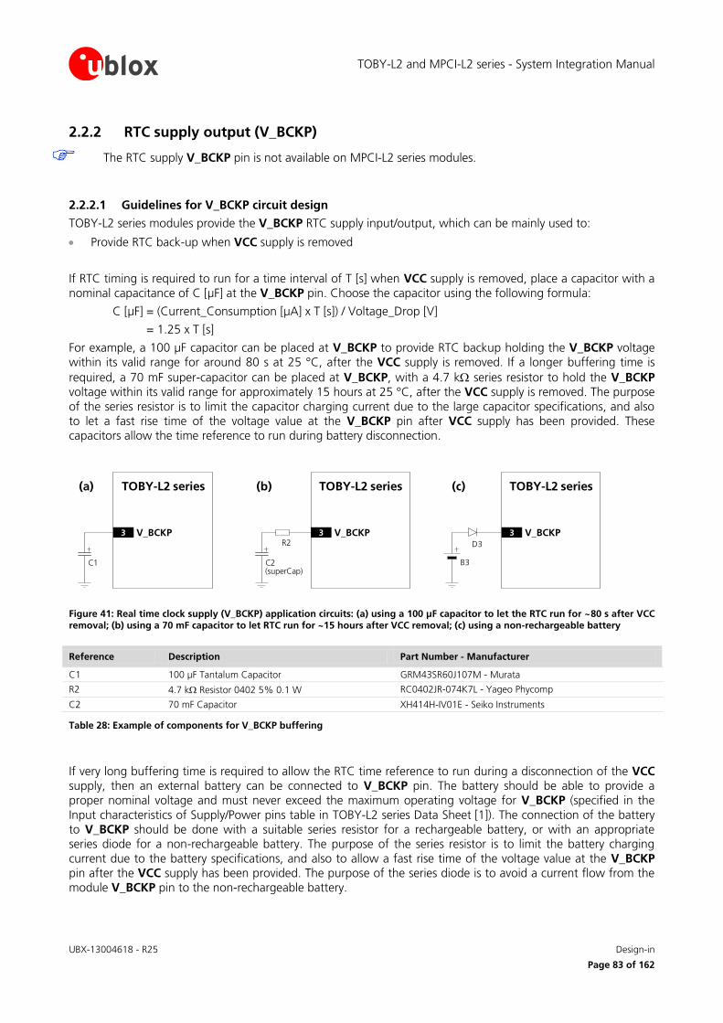
TOBY-L2 and MPCI-L2 series - System Integration Manual
UBX-13004618 - R25 Design-in
Page 83 of 162
2.2.2 RTC supply output (V_BCKP)
The RTC supply V_BCKP pin is not available on MPCI-L2 series modules.
2.2.2.1 Guidelines for V_BCKP circuit design
TOBY-L2 series modules provide the V_BCKP RTC supply input/output, which can be mainly used to:
Provide RTC back-up when VCC supply is removed
If RTC timing is required to run for a time interval of T [s] when VCC supply is removed, place a capacitor with a nominal capacitance of C [µF] at the V_BCKP pin. Choose the capacitor using the following formula:
C [µF] = (Current_Consumption [µA] x T [s]) / Voltage_Drop [V]
= 1.25 x T [s]
For example, a 100 µF capacitor can be placed at V_BCKP to provide RTC backup holding the V_BCKP voltage within its valid range for around 80 s at 25 °C, after the VCC supply is removed. If a longer buffering time is
required, a 70 mF super-capacitor can be placed at V_BCKP, with a 4.7 k series resistor to hold the V_BCKP voltage within its valid range for approximately 15 hours at 25 °C, after the VCC supply is removed. The purpose of the series resistor is to limit the capacitor charging current due to the large capacitor specifications, and also to let a fast rise time of the voltage value at the V_BCKP pin after VCC supply has been provided. These capacitors allow the time reference to run during battery disconnection.
TOBY-L2 series
C1
(a)
3 V_BCKPR2
TOBY-L2 series
C2(superCap)
(b)
3 V_BCKPD3
TOBY-L2 series
B3
(c)
3 V_BCKP
Figure 41: Real time clock supply (V_BCKP) application circuits: (a) using a 100 µF capacitor to let the RTC run for ~80 s after VCC removal; (b) using a 70 mF capacitor to let RTC run for ~15 hours after VCC removal; (c) using a non-rechargeable battery
Reference Description Part Number - Manufacturer
C1 100 µF Tantalum Capacitor GRM43SR60J107M - Murata
R2 4.7 k Resistor 0402 5% 0.1 W RC0402JR-074K7L - Yageo Phycomp
C2 70 mF Capacitor XH414H-IV01E - Seiko Instruments
Table 28: Example of components for V_BCKP buffering
If very long buffering time is required to allow the RTC time reference to run during a disconnection of the VCC supply, then an external battery can be connected to V_BCKP pin. The battery should be able to provide a proper nominal voltage and must never exceed the maximum operating voltage for V_BCKP (specified in the Input characteristics of Supply/Power pins table in TOBY-L2 series Data Sheet [1]). The connection of the battery to V_BCKP should be done with a suitable series resistor for a rechargeable battery, or with an appropriate series diode for a non-rechargeable battery. The purpose of the series resistor is to limit the battery charging current due to the battery specifications, and also to allow a fast rise time of the voltage value at the V_BCKP pin after the VCC supply has been provided. The purpose of the series diode is to avoid a current flow from the module V_BCKP pin to the non-rechargeable battery.
TOBY-L2 and MPCI-L2 series - System Integration Manual
UBX-13004618 - R25 Design-in
Page 84 of 162
If the RTC timing is not required when the VCC supply is removed, it is not needed to connect the V_BCKP pin to an external capacitor or battery. In this case the date and time are not updated when VCC is disconnected. If VCC is always supplied, then the internal regulator is supplied from the main supply and there is no need for an external component on V_BCKP.
V_BCKP supply output pin provides internal short circuit protection to limit start-up current and protect the device in short circuit situations. No additional external short circuit protection is required.
Do not apply loads which might exceed the limit for maximum available current from V_BCKP supply (see TOBY-L2 series Data Sheet [1]) as this can cause malfunctions in internal circuitry.
ESD sensitivity rating of the V_BCKP supply pin is 1 kV (Human Body Model according to JESD22-A114). Higher protection level could be required if the line is externally accessible and it can be achieved by mounting an ESD protection (e.g. EPCOS CA05P4S14THSG varistor array) close to the accessible point.
2.2.2.2 Guidelines for V_BCKP layout design
V_BCKP supply requires careful layout: avoid injecting noise on this voltage domain as it may affect the stability of the internal circuitry.
TOBY-L2 and MPCI-L2 series - System Integration Manual
UBX-13004618 - R25 Design-in
Page 85 of 162
2.2.3 Generic digital interfaces supply output (V_INT)
The generic digital interfaces supply V_INT pin is not available on MPCI-L2 series modules.
2.2.3.1 Guidelines for V_INT circuit design
TOBY-L2 series provide the V_INT generic digital interfaces 1.8 V supply output, which can be mainly used to:
Indicate when the module is switched on (as described in sections 1.6.1, 1.6.2)
Pull-up SIM detection signal (see section 2.5 for more details)
Supply voltage translators to connect 1.8 V module generic digital interfaces to 3.0 V devices (e.g. see 2.6.2)
Pull-up DDC (I2C) interface signals (see section 2.6.3 for more details)
Enable external voltage regulators providing supply for external devices, as linear LDO regulators providing the 3.3 V / 1.8 V supply rails for a u-blox ELLA-W1 series module (see section 2.6.4 for more details)
Supply an external device, as an external 1.8 V audio codec (see section 2.7.1 for more details)
V_INT supply output pin provides internal short circuit protection to limit start-up current and protect the device in short circuit situations. No additional external short circuit protection is required.
Do not apply loads which might exceed the limit for maximum available current from V_INT supply (see the TOBY-L2 series Data Sheet [1]) as this can cause malfunctions in internal circuitry.
Since the V_INT supply is generated by an internal switching step-down regulator, the V_INT voltage ripple can range as specified in the TOBY-L2 series Data Sheet [1]: it is not recommended to supply sensitive analog circuitry without adequate filtering for digital noise.
V_INT can only be used as an output: do not connect any external supply source on V_INT.
ESD sensitivity rating of the V_INT supply pin is 1 kV (Human Body Model according to JESD22-A114). Higher protection level could be required if the line is externally accessible and it can be achieved by mounting an ESD protection (e.g. EPCOS CA05P4S14THSG varistor array) close to the accessible point.
It is recommended to provide direct access to the V_INT pin on the application board by means of an accessible test point directly connected to the V_INT pin.
2.2.3.2 Guidelines for V_INT layout design
V_INT supply output is generated by an integrated switching step-down converter. Because of this, it can be a source of noise: avoid coupling with sensitive signals.
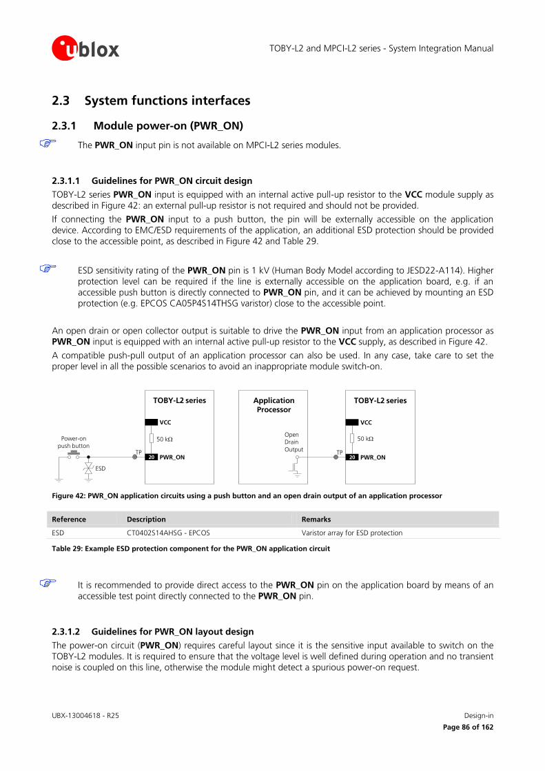
TOBY-L2 and MPCI-L2 series - System Integration Manual
UBX-13004618 - R25 Design-in
Page 86 of 162
2.3 System functions interfaces
2.3.1 Module power-on (PWR_ON)
The PWR_ON input pin is not available on MPCI-L2 series modules.
2.3.1.1 Guidelines for PWR_ON circuit design
TOBY-L2 series PWR_ON input is equipped with an internal active pull-up resistor to the VCC module supply as described in Figure 42: an external pull-up resistor is not required and should not be provided.
If connecting the PWR_ON input to a push button, the pin will be externally accessible on the application device. According to EMC/ESD requirements of the application, an additional ESD protection should be provided close to the accessible point, as described in Figure 42 and Table 29.
ESD sensitivity rating of the PWR_ON pin is 1 kV (Human Body Model according to JESD22-A114). Higher protection level can be required if the line is externally accessible on the application board, e.g. if an accessible push button is directly connected to PWR_ON pin, and it can be achieved by mounting an ESD protection (e.g. EPCOS CA05P4S14THSG varistor) close to the accessible point.
An open drain or open collector output is suitable to drive the PWR_ON input from an application processor as PWR_ON input is equipped with an internal active pull-up resistor to the VCC supply, as described in Figure 42.
A compatible push-pull output of an application processor can also be used. In any case, take care to set the proper level in all the possible scenarios to avoid an inappropriate module switch-on.
TOBY-L2 series
50 k
VCC
20 PWR_ON
Power-on push button
ESD
Open Drain
Output
Application Processor
TOBY-L2 series
50 k
VCC
20 PWR_ONTP TP
Figure 42: PWR_ON application circuits using a push button and an open drain output of an application processor
Reference Description Remarks
ESD CT0402S14AHSG - EPCOS Varistor array for ESD protection
Table 29: Example ESD protection component for the PWR_ON application circuit
It is recommended to provide direct access to the PWR_ON pin on the application board by means of an accessible test point directly connected to the PWR_ON pin.
2.3.1.2 Guidelines for PWR_ON layout design
The power-on circuit (PWR_ON) requires careful layout since it is the sensitive input available to switch on the TOBY-L2 modules. It is required to ensure that the voltage level is well defined during operation and no transient noise is coupled on this line, otherwise the module might detect a spurious power-on request.
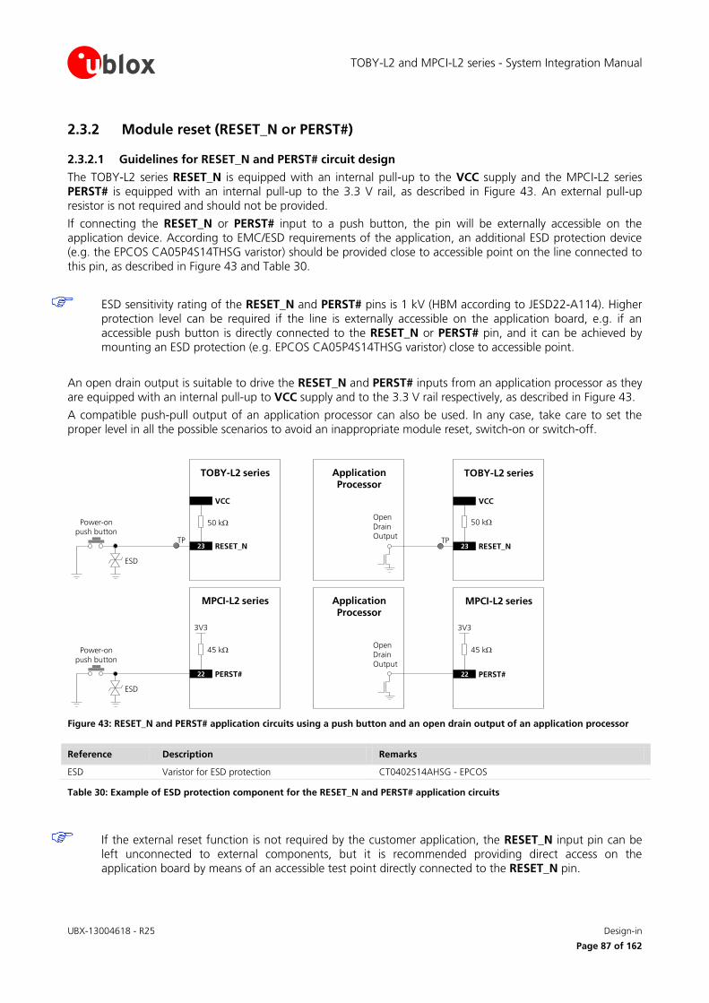
TOBY-L2 and MPCI-L2 series - System Integration Manual
UBX-13004618 - R25 Design-in
Page 87 of 162
2.3.2 Module reset (RESET_N or PERST#)
2.3.2.1 Guidelines for RESET_N and PERST# circuit design
The TOBY-L2 series RESET_N is equipped with an internal pull-up to the VCC supply and the MPCI-L2 series PERST# is equipped with an internal pull-up to the 3.3 V rail, as described in Figure 43. An external pull-up resistor is not required and should not be provided.
If connecting the RESET_N or PERST# input to a push button, the pin will be externally accessible on the application device. According to EMC/ESD requirements of the application, an additional ESD protection device (e.g. the EPCOS CA05P4S14THSG varistor) should be provided close to accessible point on the line connected to this pin, as described in Figure 43 and Table 30.
ESD sensitivity rating of the RESET_N and PERST# pins is 1 kV (HBM according to JESD22-A114). Higher protection level can be required if the line is externally accessible on the application board, e.g. if an accessible push button is directly connected to the RESET_N or PERST# pin, and it can be achieved by mounting an ESD protection (e.g. EPCOS CA05P4S14THSG varistor) close to accessible point.
An open drain output is suitable to drive the RESET_N and PERST# inputs from an application processor as they are equipped with an internal pull-up to VCC supply and to the 3.3 V rail respectively, as described in Figure 43.
A compatible push-pull output of an application processor can also be used. In any case, take care to set the proper level in all the possible scenarios to avoid an inappropriate module reset, switch-on or switch-off.
TOBY-L2 series
VCC
23 RESET_N
Power-on push button
ESD
Open
Drain Output
Application Processor
TOBY-L2 series
VCC
23 RESET_NTP TP
50 k 50 k
MPCI-L2 series
22 PERST#
Power-on
push button
ESD
Open Drain
Output
Application Processor
MPCI-L2 series
22 PERST#
45 k 45 k
3V3 3V3
Figure 43: RESET_N and PERST# application circuits using a push button and an open drain output of an application processor
Reference Description Remarks
ESD Varistor for ESD protection CT0402S14AHSG - EPCOS
Table 30: Example of ESD protection component for the RESET_N and PERST# application circuits
If the external reset function is not required by the customer application, the RESET_N input pin can be left unconnected to external components, but it is recommended providing direct access on the application board by means of an accessible test point directly connected to the RESET_N pin.
TOBY-L2 and MPCI-L2 series - System Integration Manual
UBX-13004618 - R25 Design-in
Page 88 of 162
2.3.2.2 Guidelines for RESET_N and PERST# layout design
The RESET_N and PERST# circuits require careful layout due to the pin function: ensure that the voltage level is well defined during operation and no transient noise is coupled on this line, otherwise the module might detect a spurious reset request. It is recommended to keep the connection line to RESET_N and PERST# pins as short as possible.
2.3.3 Module configuration selection by host processor
The HOST_SELECT0 and HOST_SELECT1 pins are not available on MPCI-L2 series modules.
2.3.3.1 Guidelines for HOST_SELECTx circuit design
The functionality of HOST_SELECT0 and HOST_SELECT1 pins is not supported by all the TOBY-L2 series modules product versions: the two input pins should not be driven by the host application processor or any other external device.
TOBY-L2 series modules include two input pins (HOST_SELECT0 and HOST_SELECT1) for the selection of the module configuration by the host application processor.
Do not apply voltage to HOST_SELECT0 and HOST_SELECT1 pins before the switch-on of their supply source (V_INT), to avoid latch-up of circuits and allow a proper boot of the module. If the external signals connected to the cellular module cannot be tri-stated or set low, insert a multi channel digital switch (e.g. TI SN74CB3Q16244, TS5A3159, or TS5A63157) between the two-circuit connections and set to high impedance before V_INT switch-on.
ESD sensitivity rating of the HOST_SELECT0 and HOST_SELECT1 pins is 1 kV (HBM as per JESD22-A114). Higher protection level could be required if the lines are externally accessible and it can be achieved by mounting an ESD protection (e.g. EPCOS CA05P4S14THSG varistor array) close to accessible points
If the HOST_SELECT0 and HOST_SELECT1 pins are not used, they can be left unconnected on the application board.
2.3.3.2 Guidelines for HOST_SELECTx layout design
The input pins for the selection of the module configuration by the host application processor (HOST_SELECT0 and HOST_SELECT1) are generally not critical for layout.
TOBY-L2 and MPCI-L2 series - System Integration Manual
UBX-13004618 - R25 Design-in
Page 89 of 162
2.4 Antenna interface
TOBY-L2 and MPCI-L2 series modules provide two RF interfaces for connecting the external antennas:
The ANT1 pin represents the primary RF input/output for LTE/3G/2G RF signals transmission and reception.
The ANT2 pin represents the secondary RF input for LTE MIMO 2 x 2 or 3G Rx diversity RF signals reception.
Both the ANT1 and the ANT2 pins have a nominal characteristic impedance of 50 and must be connected to
the related antenna through a 50 transmission line to allow proper transmission / reception of RF signals.
Two antennas (one connected to ANT1 pin and one connected to ANT2 pin) must be used to support the Down-Link MIMO 2 x 2 radio technology. This is a required feature for LTE category 4 User Equipments (up to 150 Mb/s Down-Link data rate) according to 3GPP specifications.
2.4.1 Antenna RF interfaces (ANT1 / ANT2)
2.4.1.1 General guidelines for antenna selection and design
The antenna is the most critical component to be evaluated. Designers must take care of the antennas from all perspective at the very start of the design phase when the physical dimensions of the application board are under analysis/decision, since the RF compliance of the device integrating TOBY-L2 and MPCI-L2 series modules with all the applicable required certification schemes depends on antennas radiating performance.
LTE/3G/2G antennas are typically available in the types of linear monopole or PCB antennas such as patches or ceramic SMT elements.
External antennas (e.g. linear monopole)
o External antennas basically do not imply physical restriction to the design of the PCB where the TOBY-L2 and MPCI-L2 series module is mounted.
o The radiation performance mainly depends on the antennas. It is required to select antennas with optimal radiating performance in the operating bands.
o RF cables should be carefully selected to have minimum insertion losses. Additional insertion loss will be introduced by low quality or long cable. Large insertion loss reduces both transmit and receive radiation performance.
o A high quality 50 RF connector provides proper PCB-to-RF-cable transition. It is recommended to strictly follow the layout and cable termination guidelines provided by the connector manufacturer.
Integrated antennas (e.g. patch-like antennas):
o Internal integrated antennas imply physical restriction to the design of the PCB:
Integrated antenna excites RF currents on its counterpoise, typically the PCB ground plane of the device that becomes part of the antenna: its dimension defines the minimum frequency that can be radiated. Therefore, the ground plane can be reduced down to a minimum size that should be similar to the quarter of the wavelength of the minimum frequency that has to be radiated, given that the orientation of the ground plane relative to the antenna element must be considered.
The isolation between the primary and the secondary antennas has to be as high as possible and the correlation between the 3D radiation patterns of the two antennas has to be as low as possible. In general, a separation of at least a quarter wavelength between the two antennas is required to achieve a good isolation and low pattern correlation.
As numerical example, the physical restriction to the PCB design can be considered as following:
Frequency = 750 MHz Wavelength = 40 cm Minimum GND plane size = 10 cm
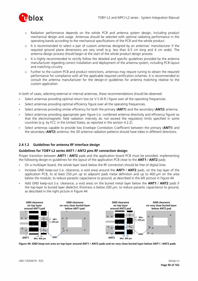
TOBY-L2 and MPCI-L2 series - System Integration Manual
UBX-13004618 - R25 Design-in
Page 90 of 162
o Radiation performance depends on the whole PCB and antenna system design, including product mechanical design and usage. Antennas should be selected with optimal radiating performance in the operating bands according to the mechanical specifications of the PCB and the whole product.
o It is recommended to select a pair of custom antennas designed by an antennas’ manufacturer if the required ground plane dimensions are very small (e.g. less than 6.5 cm long and 4 cm wide). The antenna design process should begin at the start of the whole product design process
o It is highly recommended to strictly follow the detailed and specific guidelines provided by the antenna manufacturer regarding correct installation and deployment of the antenna system, including PCB layout and matching circuitry
o Further to the custom PCB and product restrictions, antennas may require tuning to obtain the required performance for compliance with all the applicable required certification schemes. It is recommended to consult the antenna manufacturer for the design-in guidelines for antenna matching relative to the custom application
In both of cases, selecting external or internal antennas, these recommendations should be observed:
Select antennas providing optimal return loss (or V.S.W.R.) figure over all the operating frequencies.
Select antennas providing optimal efficiency figure over all the operating frequencies.
Select antennas providing similar efficiency for both the primary (ANT1) and the secondary (ANT2) antenna.
Select antennas providing appropriate gain figure (i.e. combined antenna directivity and efficiency figure) so that the electromagnetic field radiation intensity do not exceed the regulatory limits specified in some countries (e.g. by FCC in the United States, as reported in the section 4.2.2).
Select antennas capable to provide low Envelope Correlation Coefficient between the primary (ANT1) and the secondary (ANT2) antenna: the 3D antenna radiation patterns should have lobes in different directions.
2.4.1.2 Guidelines for antenna RF interface design
Guidelines for TOBY-L2 series ANT1 / ANT2 pins RF connection design
Proper transition between ANT1 / ANT2 pads and the application board PCB must be provided, implementing the following design-in guidelines for the layout of the application PCB close to the ANT1 / ANT2 pads:
On a multilayer board, the whole layer stack below the RF connection should be free of digital lines
Increase GND keep-out (i.e. clearance, a void area) around the ANT1 / ANT2 pads, on the top layer of the application PCB, to at least 250 µm up to adjacent pads metal definition and up to 400 µm on the area below the module, to reduce parasitic capacitance to ground, as described in the left picture in Figure 44
Add GND keep-out (i.e. clearance, a void area) on the buried metal layer below the ANT1 / ANT2 pads if the top-layer to buried layer dielectric thickness is below 200 µm, to reduce parasitic capacitance to ground, as described in the right picture in Figure 44
Min.
250 µm
Min. 400 µmGNDANT1
GND clearance on very close buried layer
below ANT1 pad
GND clearance on top layer
around ANT1 pad
Min.
250 µm
Min. 400 µm
GND
ANT2
GND clearance on very close buried layer
below ANT2 pad
GND clearance on top layer
around ANT2 pad
Figure 44: GND keep-out area on top layer around ANT1 / ANT2 pads and on very close buried layer below ANT1 / ANT2 pads
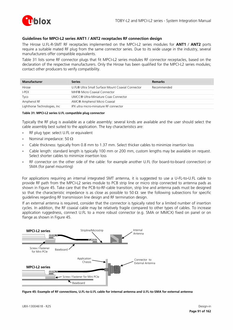
TOBY-L2 and MPCI-L2 series - System Integration Manual
UBX-13004618 - R25 Design-in
Page 91 of 162
Guidelines for MPCI-L2 series ANT1 / ANT2 receptacles RF connection design
The Hirose U.FL-R-SMT RF receptacles implemented on the MPCI-L2 series modules for ANT1 / ANT2 ports require a suitable mated RF plug from the same connector series. Due to its wide usage in the industry, several manufacturers offer compatible equivalents.
Table 31 lists some RF connector plugs that fit MPCI-L2 series modules RF connector receptacles, based on the declaration of the respective manufacturers. Only the Hirose has been qualified for the MPCI-L2 series modules; contact other producers to verify compatibility.
Manufacturer Series Remarks
Hirose U.FL® Ultra Small Surface Mount Coaxial Connector Recommended
I-PEX MHF® Micro Coaxial Connector
Tyco UMCC® Ultra-Miniature Coax Connector
Amphenol RF AMC® Amphenol Micro Coaxial
Lighthorse Technologies, Inc IPX ultra micro-miniature RF connector
Table 31: MPCI-L2 series U.FL compatible plug connector
Typically the RF plug is available as a cable assembly: several kinds are available and the user should select the cable assembly best suited to the application. The key characteristics are:
RF plug type: select U.FL or equivalent
Nominal impedance: 50
Cable thickness: typically from 0.8 mm to 1.37 mm. Select thicker cables to minimize insertion loss
Cable length: standard length is typically 100 mm or 200 mm, custom lengths may be available on request. Select shorter cables to minimize insertion loss
RF connector on the other side of the cable: for example another U.FL (for board-to-board connection) or SMA (for panel mounting)
For applications requiring an internal integrated SMT antenna, it is suggested to use a U-FL-to-U.FL cable to provide RF path from the MPCI-L2 series module to PCB strip line or micro strip connected to antenna pads as shown in Figure 45. Take care that the PCB-to-RF-cable transition, strip line and antenna pads must be designed
so that the characteristic impedance is as close as possible to 50 : see the following subsections for specific guidelines regarding RF transmission line design and RF termination design.
If an external antenna is required, consider that the connector is typically rated for a limited number of insertion cycles. In addition, the RF coaxial cable may be relatively fragile compared to other types of cables. To increase application ruggedness, connect U.FL to a more robust connector (e.g. SMA or MMCX) fixed on panel or on flange as shown in Figure 45.
MPCI-L2 series
Baseboard
Stripline/Microstrip Internal
Antenna
Baseboard
Application
ChassisConnector to
External Antenna
MPCI-L2 series
Screw / Fastener
for Mini PCIe
Screw / Fastener for Mini PCIe
Figure 45: Example of RF connections, U.FL-to-U.FL cable for internal antenna and U.FL-to-SMA for external antenna
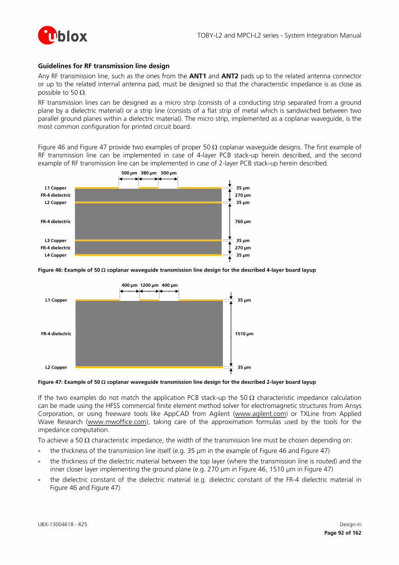
TOBY-L2 and MPCI-L2 series - System Integration Manual
UBX-13004618 - R25 Design-in
Page 92 of 162
Guidelines for RF transmission line design
Any RF transmission line, such as the ones from the ANT1 and ANT2 pads up to the related antenna connector or up to the related internal antenna pad, must be designed so that the characteristic impedance is as close as
possible to 50 .
RF transmission lines can be designed as a micro strip (consists of a conducting strip separated from a ground plane by a dielectric material) or a strip line (consists of a flat strip of metal which is sandwiched between two parallel ground planes within a dielectric material). The micro strip, implemented as a coplanar waveguide, is the most common configuration for printed circuit board.
Figure 46 and Figure 47 provide two examples of proper 50 coplanar waveguide designs. The first example of RF transmission line can be implemented in case of 4-layer PCB stack-up herein described, and the second example of RF transmission line can be implemented in case of 2-layer PCB stack-up herein described.
35 µm
35 µm
35 µm
35 µm
270 µm
270 µm
760 µm
L1 Copper
L3 Copper
L2 Copper
L4 Copper
FR-4 dielectric
FR-4 dielectric
FR-4 dielectric
380 µm 500 µm500 µm
Figure 46: Example of 50 coplanar waveguide transmission line design for the described 4-layer board layup
35 µm
35 µm
1510 µm
L2 Copper
L1 Copper
FR-4 dielectric
1200 µm 400 µm400 µm
Figure 47: Example of 50 coplanar waveguide transmission line design for the described 2-layer board layup
If the two examples do not match the application PCB stack-up the 50 characteristic impedance calculation can be made using the HFSS commercial finite element method solver for electromagnetic structures from Ansys Corporation, or using freeware tools like AppCAD from Agilent (www.agilent.com) or TXLine from Applied Wave Research (www.mwoffice.com), taking care of the approximation formulas used by the tools for the impedance computation.
To achieve a 50 characteristic impedance, the width of the transmission line must be chosen depending on:
the thickness of the transmission line itself (e.g. 35 µm in the example of Figure 46 and Figure 47)
the thickness of the dielectric material between the top layer (where the transmission line is routed) and the inner closer layer implementing the ground plane (e.g. 270 µm in Figure 46, 1510 µm in Figure 47)
the dielectric constant of the dielectric material (e.g. dielectric constant of the FR-4 dielectric material in Figure 46 and Figure 47)
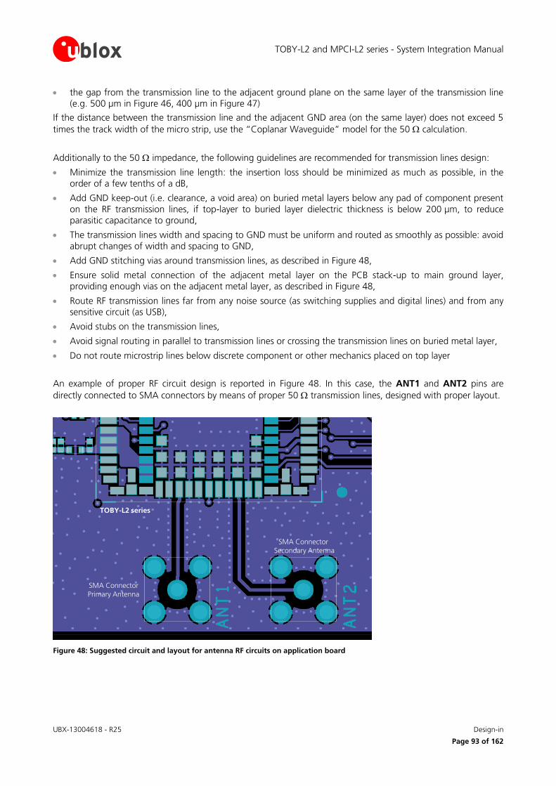
TOBY-L2 and MPCI-L2 series - System Integration Manual
UBX-13004618 - R25 Design-in
Page 93 of 162
the gap from the transmission line to the adjacent ground plane on the same layer of the transmission line (e.g. 500 µm in Figure 46, 400 µm in Figure 47)
If the distance between the transmission line and the adjacent GND area (on the same layer) does not exceed 5
times the track width of the micro strip, use the “Coplanar Waveguide” model for the 50 calculation.
Additionally to the 50 impedance, the following guidelines are recommended for transmission lines design:
Minimize the transmission line length: the insertion loss should be minimized as much as possible, in the order of a few tenths of a dB,
Add GND keep-out (i.e. clearance, a void area) on buried metal layers below any pad of component present on the RF transmission lines, if top-layer to buried layer dielectric thickness is below 200 µm, to reduce parasitic capacitance to ground,
The transmission lines width and spacing to GND must be uniform and routed as smoothly as possible: avoid abrupt changes of width and spacing to GND,
Add GND stitching vias around transmission lines, as described in Figure 48,
Ensure solid metal connection of the adjacent metal layer on the PCB stack-up to main ground layer, providing enough vias on the adjacent metal layer, as described in Figure 48,
Route RF transmission lines far from any noise source (as switching supplies and digital lines) and from any sensitive circuit (as USB),
Avoid stubs on the transmission lines,
Avoid signal routing in parallel to transmission lines or crossing the transmission lines on buried metal layer,
Do not route microstrip lines below discrete component or other mechanics placed on top layer
An example of proper RF circuit design is reported in Figure 48. In this case, the ANT1 and ANT2 pins are
directly connected to SMA connectors by means of proper 50 transmission lines, designed with proper layout.
SMA Connector
Primary Antenna
SMA Connector
Secondary Antenna
TOBY-L2 series
Figure 48: Suggested circuit and layout for antenna RF circuits on application board
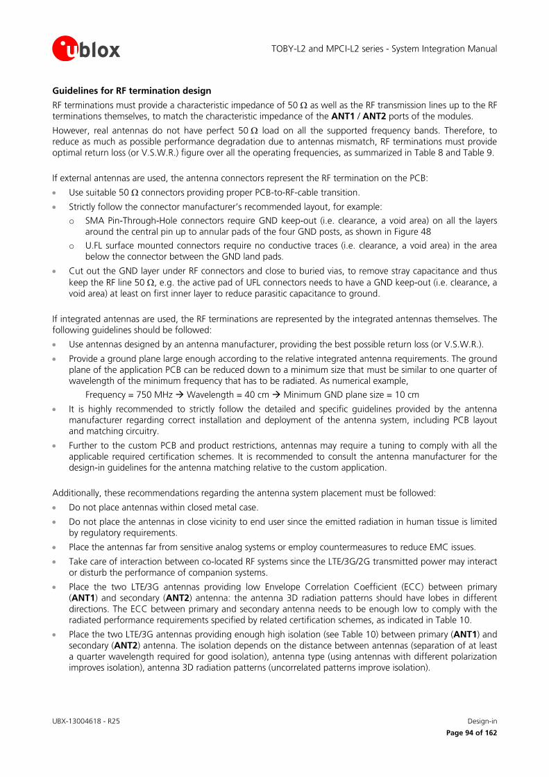
TOBY-L2 and MPCI-L2 series - System Integration Manual
UBX-13004618 - R25 Design-in
Page 94 of 162
Guidelines for RF termination design
RF terminations must provide a characteristic impedance of 50 as well as the RF transmission lines up to the RF terminations themselves, to match the characteristic impedance of the ANT1 / ANT2 ports of the modules.
However, real antennas do not have perfect 50 load on all the supported frequency bands. Therefore, to reduce as much as possible performance degradation due to antennas mismatch, RF terminations must provide optimal return loss (or V.S.W.R.) figure over all the operating frequencies, as summarized in Table 8 and Table 9.
If external antennas are used, the antenna connectors represent the RF termination on the PCB:
Use suitable 50 connectors providing proper PCB-to-RF-cable transition.
Strictly follow the connector manufacturer’s recommended layout, for example:
o SMA Pin-Through-Hole connectors require GND keep-out (i.e. clearance, a void area) on all the layers around the central pin up to annular pads of the four GND posts, as shown in Figure 48
o U.FL surface mounted connectors require no conductive traces (i.e. clearance, a void area) in the area below the connector between the GND land pads.
Cut out the GND layer under RF connectors and close to buried vias, to remove stray capacitance and thus
keep the RF line 50 , e.g. the active pad of UFL connectors needs to have a GND keep-out (i.e. clearance, a void area) at least on first inner layer to reduce parasitic capacitance to ground.
If integrated antennas are used, the RF terminations are represented by the integrated antennas themselves. The following guidelines should be followed:
Use antennas designed by an antenna manufacturer, providing the best possible return loss (or V.S.W.R.).
Provide a ground plane large enough according to the relative integrated antenna requirements. The ground plane of the application PCB can be reduced down to a minimum size that must be similar to one quarter of wavelength of the minimum frequency that has to be radiated. As numerical example,
Frequency = 750 MHz Wavelength = 40 cm Minimum GND plane size = 10 cm
It is highly recommended to strictly follow the detailed and specific guidelines provided by the antenna manufacturer regarding correct installation and deployment of the antenna system, including PCB layout and matching circuitry.
Further to the custom PCB and product restrictions, antennas may require a tuning to comply with all the applicable required certification schemes. It is recommended to consult the antenna manufacturer for the design-in guidelines for the antenna matching relative to the custom application.
Additionally, these recommendations regarding the antenna system placement must be followed:
Do not place antennas within closed metal case.
Do not place the antennas in close vicinity to end user since the emitted radiation in human tissue is limited by regulatory requirements.
Place the antennas far from sensitive analog systems or employ countermeasures to reduce EMC issues.
Take care of interaction between co-located RF systems since the LTE/3G/2G transmitted power may interact or disturb the performance of companion systems.
Place the two LTE/3G antennas providing low Envelope Correlation Coefficient (ECC) between primary (ANT1) and secondary (ANT2) antenna: the antenna 3D radiation patterns should have lobes in different directions. The ECC between primary and secondary antenna needs to be enough low to comply with the radiated performance requirements specified by related certification schemes, as indicated in Table 10.
Place the two LTE/3G antennas providing enough high isolation (see Table 10) between primary (ANT1) and secondary (ANT2) antenna. The isolation depends on the distance between antennas (separation of at least a quarter wavelength required for good isolation), antenna type (using antennas with different polarization improves isolation), antenna 3D radiation patterns (uncorrelated patterns improve isolation).
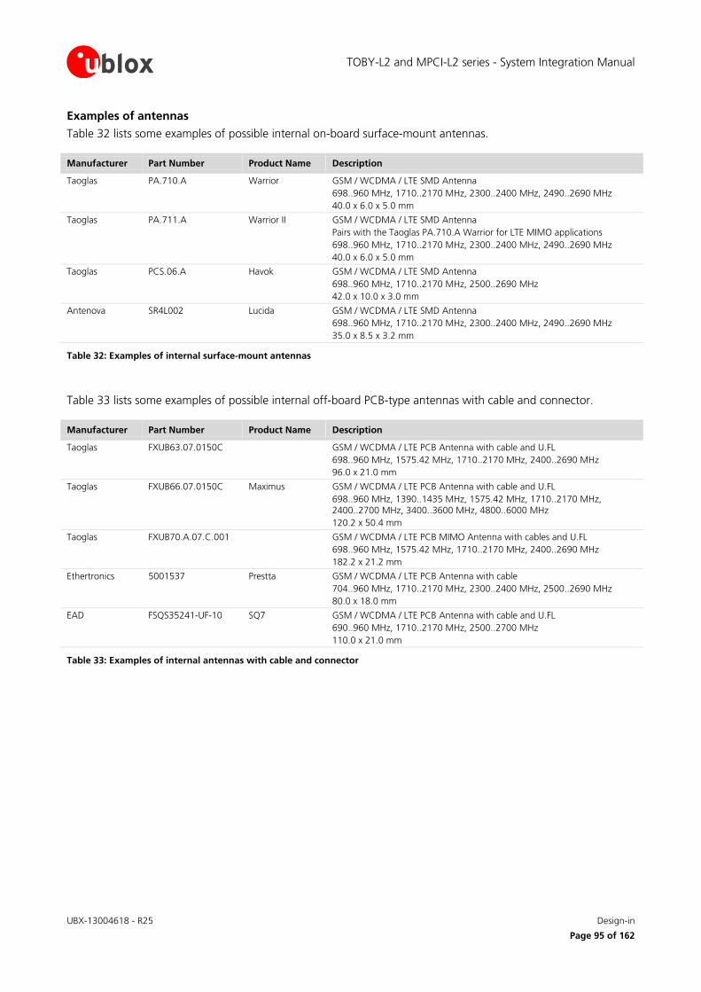
TOBY-L2 and MPCI-L2 series - System Integration Manual
UBX-13004618 - R25 Design-in
Page 95 of 162
Examples of antennas
Table 32 lists some examples of possible internal on-board surface-mount antennas.
Manufacturer Part Number Product Name Description
Taoglas PA.710.A Warrior GSM / WCDMA / LTE SMD Antenna
698..960 MHz, 1710..2170 MHz, 2300..2400 MHz, 2490..2690 MHz
40.0 x 6.0 x 5.0 mm
Taoglas PA.711.A Warrior II GSM / WCDMA / LTE SMD Antenna
Pairs with the Taoglas PA.710.A Warrior for LTE MIMO applications
698..960 MHz, 1710..2170 MHz, 2300..2400 MHz, 2490..2690 MHz
40.0 x 6.0 x 5.0 mm
Taoglas PCS.06.A Havok GSM / WCDMA / LTE SMD Antenna
698..960 MHz, 1710..2170 MHz, 2500..2690 MHz
42.0 x 10.0 x 3.0 mm
Antenova SR4L002 Lucida GSM / WCDMA / LTE SMD Antenna
698..960 MHz, 1710..2170 MHz, 2300..2400 MHz, 2490..2690 MHz
35.0 x 8.5 x 3.2 mm
Table 32: Examples of internal surface-mount antennas
Table 33 lists some examples of possible internal off-board PCB-type antennas with cable and connector.
Manufacturer Part Number Product Name Description
Taoglas FXUB63.07.0150C GSM / WCDMA / LTE PCB Antenna with cable and U.FL
698..960 MHz, 1575.42 MHz, 1710..2170 MHz, 2400..2690 MHz
96.0 x 21.0 mm
Taoglas FXUB66.07.0150C Maximus GSM / WCDMA / LTE PCB Antenna with cable and U.FL
698..960 MHz, 1390..1435 MHz, 1575.42 MHz, 1710..2170 MHz, 2400..2700 MHz, 3400..3600 MHz, 4800..6000 MHz
120.2 x 50.4 mm
Taoglas FXUB70.A.07.C.001 GSM / WCDMA / LTE PCB MIMO Antenna with cables and U.FL
698..960 MHz, 1575.42 MHz, 1710..2170 MHz, 2400..2690 MHz
182.2 x 21.2 mm
Ethertronics 5001537 Prestta GSM / WCDMA / LTE PCB Antenna with cable
704..960 MHz, 1710..2170 MHz, 2300..2400 MHz, 2500..2690 MHz
80.0 x 18.0 mm
EAD FSQS35241-UF-10 SQ7 GSM / WCDMA / LTE PCB Antenna with cable and U.FL
690..960 MHz, 1710..2170 MHz, 2500..2700 MHz
110.0 x 21.0 mm
Table 33: Examples of internal antennas with cable and connector
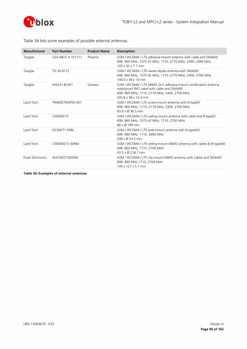
TOBY-L2 and MPCI-L2 series - System Integration Manual
UBX-13004618 - R25 Design-in
Page 96 of 162
Table 34 lists some examples of possible external antennas.
Manufacturer Part Number Product Name Description
Taoglas GSA.8827.A.101111 Phoenix GSM / WCDMA / LTE adhesive-mount antenna with cable and SMA(M)
698..960 MHz, 1575.42 MHz, 1710..2170 MHz, 2490..2690 MHz
105 x 30 x 7.7 mm
Taoglas TG.30.8112 GSM / WCDMA / LTE swivel dipole antenna with SMA(M)
698..960 MHz, 1575.42 MHz, 1710..2170 MHz, 2400..2700 MHz
148.6 x 49 x 10 mm
Taoglas MA241.BI.001 Genesis GSM / WCDMA / LTE MIMO 2in1 adhesive-mount combination antenna
waterproof IP67 rated with cable and SMA(M)
698..960 MHz, 1710..2170 MHz, 2400..2700 MHz
205.8 x 58 x 12.4 mm
Laird Tech. TRA6927M3PW-001 GSM / WCDMA / LTE screw-mount antenna with N-type(F)
698..960 MHz, 1710..2170 MHz, 2300..2700 MHz
83.8 x Ø 36.5 mm
Laird Tech. CMS69273 GSM / WCDMA / LTE ceiling-mount antenna with cable and N-type(F)
698..960 MHz, 1575.42 MHz, 1710..2700 MHz
86 x Ø 199 mm
Laird Tech. OC69271-FNM GSM / WCDMA / LTE pole-mount antenna with N-type(M)
698..960 MHz, 1710..2690 MHz
248 x Ø 24.5 mm
Laird Tech. CMD69273-30NM GSM / WCDMA / LTE ceiling-mount MIMO antenna with cables & N-type(M)
698..960 MHz, 1710..2700 MHz
43.5 x Ø 218.7 mm
Pulse Electronics WA700/2700SMA GSM / WCDMA / LTE clip-mount MIMO antenna with cables and SMA(M)
698..960 MHz,1710..2700 MHz
149 x 127 x 5.1 mm
Table 34: Examples of external antennas
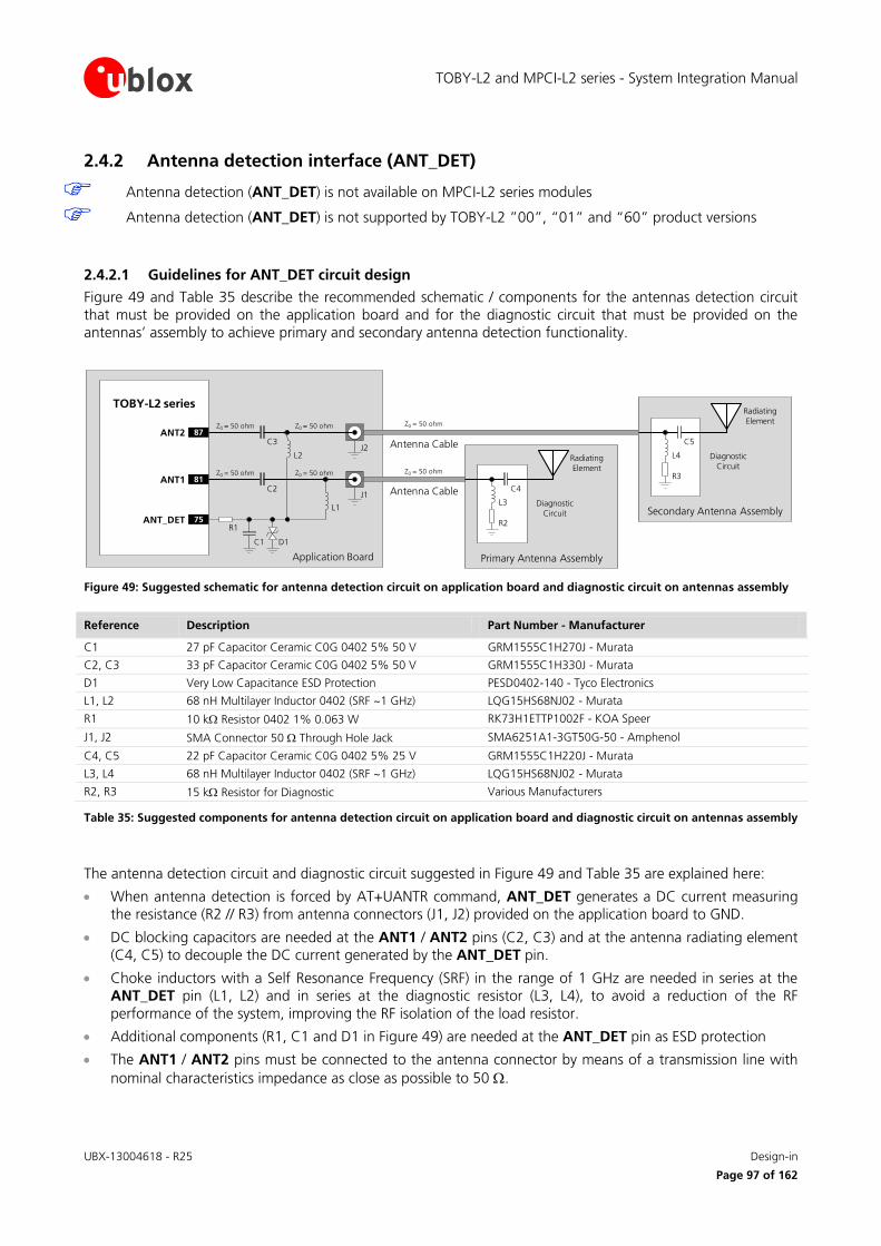
TOBY-L2 and MPCI-L2 series - System Integration Manual
UBX-13004618 - R25 Design-in
Page 97 of 162
2.4.2 Antenna detection interface (ANT_DET)
Antenna detection (ANT_DET) is not available on MPCI-L2 series modules
Antenna detection (ANT_DET) is not supported by TOBY-L2 ”00”, “01” and “60” product versions
2.4.2.1 Guidelines for ANT_DET circuit design
Figure 49 and Table 35 describe the recommended schematic / components for the antennas detection circuit that must be provided on the application board and for the diagnostic circuit that must be provided on the antennas’ assembly to achieve primary and secondary antenna detection functionality.
Application Board
Antenna Cable
TOBY-L2 series
81ANT1
75ANT_DETR1
C1 D1
C2J1
Z0 = 50 ohm Z0 = 50 ohm Z0 = 50 ohm
Primary Antenna Assembly
R2
C4
L3
Radiating
Element
Diagnostic
Circuit
L2
L1
Antenna Cable87ANT2
C3J2
Z0 = 50 ohm Z0 = 50 ohm Z0 = 50 ohm
Secondary Antenna Assembly
R3
C5
L4
Radiating Element
Diagnostic
Circuit
Figure 49: Suggested schematic for antenna detection circuit on application board and diagnostic circuit on antennas assembly
Reference Description Part Number - Manufacturer
C1 27 pF Capacitor Ceramic C0G 0402 5% 50 V GRM1555C1H270J - Murata
C2, C3 33 pF Capacitor Ceramic C0G 0402 5% 50 V GRM1555C1H330J - Murata
D1 Very Low Capacitance ESD Protection PESD0402-140 - Tyco Electronics
L1, L2 68 nH Multilayer Inductor 0402 (SRF ~1 GHz) LQG15HS68NJ02 - Murata
R1 10 k Resistor 0402 1% 0.063 W RK73H1ETTP1002F - KOA Speer
J1, J2 SMA Connector 50 Through Hole Jack SMA6251A1-3GT50G-50 - Amphenol
C4, C5 22 pF Capacitor Ceramic C0G 0402 5% 25 V GRM1555C1H220J - Murata
L3, L4 68 nH Multilayer Inductor 0402 (SRF ~1 GHz) LQG15HS68NJ02 - Murata
R2, R3 15 k Resistor for Diagnostic Various Manufacturers
Table 35: Suggested components for antenna detection circuit on application board and diagnostic circuit on antennas assembly
The antenna detection circuit and diagnostic circuit suggested in Figure 49 and Table 35 are explained here:
When antenna detection is forced by AT+UANTR command, ANT_DET generates a DC current measuring the resistance (R2 // R3) from antenna connectors (J1, J2) provided on the application board to GND.
DC blocking capacitors are needed at the ANT1 / ANT2 pins (C2, C3) and at the antenna radiating element (C4, C5) to decouple the DC current generated by the ANT_DET pin.
Choke inductors with a Self Resonance Frequency (SRF) in the range of 1 GHz are needed in series at the ANT_DET pin (L1, L2) and in series at the diagnostic resistor (L3, L4), to avoid a reduction of the RF performance of the system, improving the RF isolation of the load resistor.
Additional components (R1, C1 and D1 in Figure 49) are needed at the ANT_DET pin as ESD protection
The ANT1 / ANT2 pins must be connected to the antenna connector by means of a transmission line with
nominal characteristics impedance as close as possible to 50 .
TOBY-L2 and MPCI-L2 series - System Integration Manual
UBX-13004618 - R25 Design-in
Page 98 of 162
The DC impedance at RF port for some antennas may be a DC open (e.g. linear monopole) or a DC short to reference GND (e.g. PIFA antenna). For those antennas, without the diagnostic circuit of Figure 49, the measured DC resistance is always at the limits of the measurement range (respectively open or short), and there is no means to distinguish between a defect on antenna path with similar characteristics (respectively: removal of linear antenna or RF cable shorted to GND for PIFA antenna).
Furthermore, any other DC signal injected to the RF connection from ANT connector to radiating element will alter the measurement and produce invalid results for antenna detection.
It is recommended to use an antenna with a built-in diagnostic resistor in the range from 5 k to 30 k to assure good antenna detection functionality and avoid a reduction of module RF performance. The choke inductor should exhibit a parallel Self Resonance Frequency (SRF) in the range of 1 GHz to improve the RF isolation of load resistor.
For example:
Consider an antenna with built-in DC load resistor of 15 k. Using the +UANTR AT command, the module reports the resistance value evaluated from the antenna connector provided on the application board to GND:
Reported values close to the used diagnostic resistor nominal value (i.e. values from 13 k to 17 k if a
15 k diagnostic resistor is used) indicate that the antenna is properly connected.
Values close to the measurement range maximum limit (approximately 50 k) or an open-circuit “over range” report (see u-blox AT Commands Manual [3]) means that that the antenna is not connected or the RF cable is broken.
Reported values below the measurement range minimum limit (1 k) highlights a short to GND at antenna or along the RF cable.
Measurement inside the valid measurement range and outside the expected range may indicate an improper connection, damaged antenna or wrong value of antenna load resistor for diagnostic.
Reported value could differ from the real resistance value of the diagnostic resistor mounted inside the antenna assembly due to antenna cable length, antenna cable capacity and the used measurement method.
If the primary / secondary antenna detection function is not required by the customer application, the ANT_DET pin can be left not connected and the ANT1 / ANT2 pins can be directly connected to the
related antenna connector by means of a 50 transmission line as described in Figure 48.
2.4.2.2 Guidelines for ANT_DET layout design
The recommended layout for the primary antenna detection circuit to be provided on the application board to achieve the primary antenna detection functionality, implementing the recommended schematic described in Figure 49 and Table 35, is explained here:
The ANT1 / ANT2 pins have to be connected to the antenna connector by means of a 50 transmission line, implementing the design guidelines described in section 2.4.1 and the recommendations of the SMA connector manufacturer.
DC blocking capacitor at ANT1 / ANT2 pins (C2, C3) has to be placed in series to the 50 RF line.
The ANT_DET pin has to be connected to the 50 transmission line by means of a sense line.
Choke inductors in series at the ANT_DET pin (L1, L2) have to be placed so that one pad is on the 50 transmission line and the other pad represents the start of the sense line to the ANT_DET pin.
The additional components (R1, C1 and D1) on the ANT_DET line have to be placed as ESD protection.
TOBY-L2 and MPCI-L2 series - System Integration Manual
UBX-13004618 - R25 Design-in
Page 99 of 162
2.5 SIM interface
SIM detection interface (GPIO5) is not available on the MPCI-L2 series modules.
SIM detection interface (GPIO5) is not supported by the TOBY-L2 modules “00”, “01” and “60” product versions: the pin should not be driven by any external device.
2.5.1 Guidelines for SIM circuit design
Guidelines for SIM cards, SIM connectors and SIM chips selection
The ISO/IEC 7816, the ETSI TS 102 221 and the ETSI TS 102 671 specifications define the physical, electrical and functional characteristics of Universal Integrated Circuit Cards (UICC), which contains the Subscriber Identification Module (SIM) integrated circuit that securely stores all the information needed to identify and authenticate subscribers over the LTE/3G/2G network.
Removable UICC / SIM card contacts mapping is defined by ISO/IEC 7816 and ETSI TS 102 221 as follows:
Contact C1 = VCC (Supply) It must be connected to VSIM or UIM_PWR
Contact C2 = RST (Reset) It must be connected to SIM_RST or UIM_RESET
Contact C3 = CLK (Clock) It must be connected to SIM_CLK or UIM_CLK
Contact C4 = AUX1 (Auxiliary contact) It must be left not connected
Contact C5 = GND (Ground) It must be connected to GND
Contact C6 = VPP (Programming supply) It can be left not connected
Contact C7 = I/O (Data input/output) It must be connected to SIM_IO or UIM_DATA
Contact C8 = AUX2 (Auxiliary contact) It must be left not connected
A removable SIM card can have 6 contacts (C1, C2, C3, C5, C6, C7) or 8 contacts, also including the auxiliary contacts C4 and C8. Only 6 contacts are required and must be connected to the module SIM interface.
Removable SIM cards are suitable for applications requiring a change of SIM card during the product lifetime.
A SIM card holder can have 6 or 8 positions if a mechanical card presence detector is not provided, or it can have 6+2 or 8+2 positions if two additional pins relative to the normally-open mechanical switch integrated in the SIM connector for the mechanical card presence detection are provided. Select a SIM connector providing 6+2 or 8+2 positions if the optional SIM detection feature (not available on MPCI-L2 series) is required by the custom application, otherwise a connector without integrated mechanical presence switch can be selected.
Solderable UICC / SIM chip contact mapping (M2M UICC Form Factor) is defined by ETSI TS 102 671 as:
Case Pin 8 = UICC Contact C1 = VCC (Supply) It must be connected to VSIM or UIM_PWR
Case Pin 7 = UICC Contact C2 = RST (Reset) It must be connected to SIM_RST or UIM_RESET
Case Pin 6 = UICC Contact C3 = CLK (Clock) It must be connected to SIM_CLK or UIM_CLK
Case Pin 5 = UICC Contact C4 = AUX1 (Aux.contact) It must be left not connected
Case Pin 1 = UICC Contact C5 = GND (Ground) It must be connected to GND
Case Pin 2 = UICC Contact C6 = VPP (Progr. supply) It can be left not connected
Case Pin 3 = UICC Contact C7 = I/O (Data I/O) It must be connected to SIM_IO or UIM_DATA
Case Pin 4 = UICC Contact C8 = AUX2 (Aux. contact) It must be left not connected
A solderable SIM chip has 8 contacts and can also include the auxiliary contacts C4 and C8 for other uses, but only 6 contacts are required and must be connected to the module SIM card interface as described above.
Solderable SIM chips are suitable for M2M applications where it is not required to change the SIM once installed.
TOBY-L2 and MPCI-L2 series - System Integration Manual
UBX-13004618 - R25 Design-in
Page 100 of 162
Guidelines for single SIM card connection without detection
A removable SIM card placed in a SIM card holder must be connected to the SIM card interface of TOBY-L2 and MPCI-L2 series modules as described in Figure 50, where the optional SIM detection feature is not implemented.
Follow these guidelines to connect the module to a SIM connector without SIM presence detection:
Connect the UICC / SIM contacts C1 (VCC) to the VSIM / UIM_PWR pin of the module.
Connect the UICC / SIM contact C7 (I/O) to the SIM_IO / UIM_DATA pin of the module.
Connect the UICC / SIM contact C3 (CLK) to the SIM_CLK / UIM_CLK pin of the module.
Connect the UICC / SIM contact C2 (RST) to the SIM_RST / UIM_RESET pin of the module.
Connect the UICC / SIM contact C5 (GND) to ground.
Provide a 100 nF bypass capacitor (e.g. Murata GRM155R71C104K) on SIM supply line, close to the relative pad of the SIM connector, to prevent digital noise.
Provide a bypass capacitor of about 22 pF to 47 pF (e.g. Murata GRM1555C1H470J) on each SIM line, very close to each related pad of the SIM connector, to prevent RF coupling especially in case the RF antenna is placed closer than 10 - 30 cm from the SIM card holder.
Provide a very low capacitance (i.e. less than 10 pF) ESD protection (e.g. Tyco PESD0402-140) on each externally accessible SIM line, close to each relative pad of the SIM connector. ESD sensitivity rating of the SIM interface pins is 1 kV (HBM). So that, according to EMC/ESD requirements of the custom application, higher protection level can be required if the lines are externally accessible on the application device.
Limit capacitance and series resistance on each SIM signal to match the SIM requirements (26.2 ns is the maximum allowed rise time on clock line, 1.0 µs is the maximum allowed rise time on data and reset lines).
TOBY-L2 series
59VSIM
57SIM_IO
56SIM_CLK
58SIM_RST
SIM CARD
HOLDER
C5
C6
C7
C
1
C
2
C
3
SIM Card Bottom View
(contacts side)C1
VPP (C6)
VCC (C1)
IO (C7)
CLK (C3)
RST (C2)
GND (C5)C2 C3 C5
J1
C4 D1 D2 D3 D4
C8
C
4
MPCI-L2 series
8UIM_PWR
10UIM_DATA
12UIM_CLK
14UIM_RESET
SIM CARD HOLDER
C
5
C
6
C
7
C
1
C
2
C
3
SIM Card Bottom View
(contacts side)C1
VPP (C6)
VCC (C1)
IO (C7)
CLK (C3)
RST (C2)
GND (C5)C2 C3 C5
J1
C4 D1 D2 D3 D4
C
8
C
4
Figure 50: Application circuits for the connection to a single removable SIM card, with SIM detection not implemented
Reference Description Part Number - Manufacturer
C1, C2, C3, C4 47 pF Capacitor Ceramic C0G 0402 5% 50 V GRM1555C1H470JA01 - Murata
C5 100 nF Capacitor Ceramic X7R 0402 10% 16 V GRM155R71C104KA01 - Murata
D1, D2, D3, D4 Very Low Capacitance ESD Protection PESD0402-140 - Tyco Electronics
J1 SIM Card Holder, 6 p, without card presence switch Various manufacturers, as C707 10M006 136 2 - Amphenol
Table 36: Example of components for the connection to a single removable SIM card, with SIM detection not implemented
TOBY-L2 and MPCI-L2 series - System Integration Manual
UBX-13004618 - R25 Design-in
Page 101 of 162
Guidelines for single SIM chip connection
A solderable SIM chip (M2M UICC Form Factor) must be connected the SIM card interface of TOBY-L2 and MPCI-L2 series modules as described in Figure 51.
Follow these guidelines to connect the module to a solderable SIM chip without SIM presence detection:
Connect the UICC / SIM contacts C1 (VCC) to the VSIM / UIM_PWR pin of the module.
Connect the UICC / SIM contact C7 (I/O) to the SIM_IO / UIM_DATA pin of the module.
Connect the UICC / SIM contact C3 (CLK) to the SIM_CLK / UIM_CLK pin of the module.
Connect the UICC / SIM contact C2 (RST) to the SIM_RST / UIM_RESET pin of the module.
Connect the UICC / SIM contact C5 (GND) to ground.
Provide a 100 nF bypass capacitor (e.g. Murata GRM155R71C104K) at the SIM supply line close to the relative pad of the SIM chip, to prevent digital noise.
Provide a bypass capacitor of about 22 pF to 47 pF (e.g. Murata GRM1555C1H470J) on each SIM line, to prevent RF coupling especially in case the RF antenna is placed closer than 10 - 30 cm from the SIM lines.
Limit capacitance and series resistance on each SIM signal to match the SIM requirements (26.2 ns is the maximum allowed rise time on clock line, 1.0 µs is the maximum allowed rise time on data and reset lines).
TOBY-L2 series
59VSIM
57SIM_IO
56SIM_CLK
58SIM_RST
SIM CHIP
SIM ChipBottom View
(contacts side)C1
VPP (C6)
VCC (C1)
IO (C7)
CLK (C3)
RST (C2)
GND (C5)C2 C3 C5
U1
C4
2
8
3
6
7
1
C1 C5
C2 C6
C3 C7
C4 C8
8
7
6
5
1
2
3
4
MPCI-L2 series
8UIM_PWR
10UIM_DATA
12UIM_CLK
14UIM_RESET
SIM CHIP
SIM ChipBottom View
(contacts side)C1
VPP (C6)
VCC (C1)
IO (C7)
CLK (C3)
RST (C2)
GND (C5)C2 C3 C5
U1
C4
2
8
3
6
7
1
C1 C5
C2 C6
C3 C7
C4 C8
8
7
6
5
1
2
3
4
Figure 51: Application circuits for the connection to a single solderable SIM chip, with SIM detection not implemented
Reference Description Part Number - Manufacturer
C1, C2, C3, C4 47 pF Capacitor Ceramic C0G 0402 5% 50 V GRM1555C1H470JA01 - Murata
C5 100 nF Capacitor Ceramic X7R 0402 10% 16 V GRM155R71C104KA01 - Murata
U1 SIM chip (M2M UICC Form Factor) Various Manufacturers
Table 37: Example of components for the connection to a single solderable SIM chip, with SIM detection not implemented
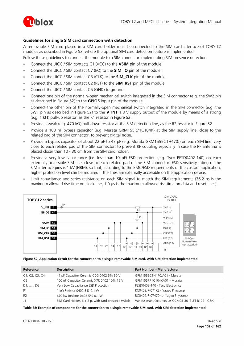
TOBY-L2 and MPCI-L2 series - System Integration Manual
UBX-13004618 - R25 Design-in
Page 102 of 162
Guidelines for single SIM card connection with detection
A removable SIM card placed in a SIM card holder must be connected to the SIM card interface of TOBY-L2 modules as described in Figure 52, where the optional SIM card detection feature is implemented.
Follow these guidelines to connect the module to a SIM connector implementing SIM presence detection:
Connect the UICC / SIM contacts C1 (VCC) to the VSIM pin of the module.
Connect the UICC / SIM contact C7 (I/O) to the SIM_IO pin of the module.
Connect the UICC / SIM contact C3 (CLK) to the SIM_CLK pin of the module.
Connect the UICC / SIM contact C2 (RST) to the SIM_RST pin of the module.
Connect the UICC / SIM contact C5 (GND) to ground.
Connect one pin of the normally-open mechanical switch integrated in the SIM connector (e.g. the SW2 pin as described in Figure 52) to the GPIO5 input pin of the module.
Connect the other pin of the normally-open mechanical switch integrated in the SIM connector (e.g. the SW1 pin as described in Figure 52) to the V_INT 1.8 V supply output of the module by means of a strong
(e.g. 1 k) pull-up resistor, as the R1 resistor in Figure 52.
Provide a weak (e.g. 470 k) pull-down resistor at the SIM detection line, as the R2 resistor in Figure 52
Provide a 100 nF bypass capacitor (e.g. Murata GRM155R71C104K) at the SIM supply line, close to the related pad of the SIM connector, to prevent digital noise.
Provide a bypass capacitor of about 22 pF to 47 pF (e.g. Murata GRM1555C1H470J) on each SIM line, very close to each related pad of the SIM connector, to prevent RF coupling especially in case the RF antenna is placed closer than 10 - 30 cm from the SIM card holder.
Provide a very low capacitance (i.e. less than 10 pF) ESD protection (e.g. Tyco PESD0402-140) on each externally accessible SIM line, close to each related pad of the SIM connector: ESD sensitivity rating of the SIM interface pins is 1 kV (HBM), so that, according to the EMC/ESD requirements of the custom application, higher protection level can be required if the lines are externally accessible on the application device.
Limit capacitance and series resistance on each SIM signal to match the SIM requirements (26.2 ns is the maximum allowed rise time on clock line, 1.0 µs is the maximum allowed rise time on data and reset lines).
TOBY-L2 series
5V_INT
60GPIO5
SIM CARD
HOLDER
C
5
C
6
C
7
C
1
C
2
C
3
SIM Card Bottom View (contacts side)
C1
VPP (C6)
VCC (C1)
IO (C7)
CLK (C3)
RST (C2)
GND (C5)C2 C3 C5
J1
C4
SW1
SW2
D1 D2 D3 D4 D5 D6
R2
R1
C
8
C
4
TP
59VSIM
57SIM_IO
56SIM_CLK
58SIM_RST
Figure 52: Application circuit for the connection to a single removable SIM card, with SIM detection implemented
Reference Description Part Number - Manufacturer
C1, C2, C3, C4 47 pF Capacitor Ceramic C0G 0402 5% 50 V GRM1555C1H470JA01 - Murata
C5 100 nF Capacitor Ceramic X7R 0402 10% 16 V GRM155R71C104KA01 - Murata
D1, … , D6 Very Low Capacitance ESD Protection PESD0402-140 - Tyco Electronics
R1 1 k Resistor 0402 5% 0.1 W RC0402JR-071KL - Yageo Phycomp
R2 470 k Resistor 0402 5% 0.1 W RC0402JR-07470KL- Yageo Phycomp
J1 SIM Card Holder, 6 + 2 p, with card presence switch Various manufacturers, as CCM03-3013LFT R102 - C&K
Table 38: Example of components for the connection to a single removable SIM card, with SIM detection implemented
TOBY-L2 and MPCI-L2 series - System Integration Manual
UBX-13004618 - R25 Design-in
Page 103 of 162
Guidelines for dual SIM card / chip connection
Two SIM card / chip can be connected to the SIM interface of TOBY-L2 and MPCI-L2 series modules as described in the application circuits of Figure 53.
TOBY-L2 and MPCI-L2 series modules do not support the usage of two SIM at the same time, but two SIM can be populated on the application board, providing a proper switch to connect only the first or only the second SIM at a time to the SIM interface of the modules, as described in Figure 53.
TOBY-L2 modules “00”, “01” and “60” product versions and MPCI-L2 modules do not support SIM hot insertion / removal functionality, to enable / disable SIM interface upon detection of external SIM card physical insertion / removal: the physical connection between the external SIM and the module has to be provided before the module boot and then held for normal operation. Switching from one SIM to another can only be properly done within one of these two time periods:
after TOBY-L2 module switch-off by the AT+CPWROFF and before TOBY-L2 module switch-on by PWR_ON
after TOBY-L2 / MPCI-L2 module deregistration from network by AT+COPS=2 or by AT+CFUN=4 and before TOBY-L2 / MPCI-L2 module reset (reboot) by AT+CFUN=16 or AT+CFUN=1,1
TOBY-L2 modules (except “00”, “01” and “60” product versions) support SIM hot insertion / removal on the GPIO5 pin: if the feature is enabled using the specific AT commands (see sections 1.8.2 and 1.11, and u-blox AT Commands Manual [3], +UGPIOC, +UDCONF=50 commands), the switch from first SIM to the second SIM can be properly done when a Low logic level is present on the GPIO5 pin (“SIM not inserted” = SIM interface not enabled), without the necessity of a module re-boot, so that the SIM interface will be re-enabled by the module to use the second SIM when a high logic level is re-applied on the GPIO5 pin.
In the application circuit example represented in Figure 53, the application processor will drive the SIM switch using its own GPIO to properly select the SIM that is used by the module. Another GPIO may be used to handle the SIM hot insertion / removal function of TOBY-L2 modules, which can also be handled by other external circuits or by the cellular module GPIO according to the application requirements.
The dual SIM connection circuit described in Figure 53 can be implemented for SIM chips as well, providing proper connection between SIM switch and SIM chip as described in Figure 51.
If it is required to switch between more than 2 SIM, a circuit similar to the one described in Figure 53 can be implemented: in case of 4 SIM circuit, using proper 4-throw switch instead of the suggested 2-throw switches.
Follow these guidelines to connect the module to two external SIM connectors:
Use a proper low on resistance (i.e. few ohms) and low on capacitance (i.e. few pF) 2-throw analog switch (e.g. Fairchild FSA2567) as SIM switch to ensure high-speed data transfer according to SIM requirements.
Connect the contacts C1 (VCC) and C6 (VPP) of the two UICC / SIM to the VSIM / UIM_PWR pin of the module by means of a proper 2-throw analog switch (e.g. Fairchild FSA2567).
Connect the contact C7 (I/O) of the two UICC / SIM to the SIM_IO / UIM_DATA pin of the module by means of a proper 2-throw analog switch (e.g. Fairchild FSA2567).
Connect the contact C3 (CLK) of the two UICC / SIM to the SIM_CLK / UIM_CLK pin of the module by means of a proper 2-throw analog switch (e.g. Fairchild FSA2567).
Connect the contact C2 (RST) of the two UICC / SIM to the SIM_RST / UIM_RESET pin of the module by means of a proper 2-throw analog switch (e.g. Fairchild FSA2567).
Connect the contact C5 (GND) of the two UICC / SIM to ground.
Provide a 100 nF bypass capacitor (e.g. Murata GRM155R71C104K) at the SIM supply (VSIM / UIM_PWR), close to the related pad of the two SIM connectors, to prevent digital noise.
Provide a bypass capacitor of about 22 pF to 47 pF (e.g. Murata GRM1555C1H470J) on each SIM line, very close to each related pad of the two SIM connectors, to prevent RF coupling especially in case the RF antenna is placed closer than 10 - 30 cm from the SIM card holders.
Provide a very low capacitance (i.e. less than 10 pF) ESD protection (e.g. Tyco Electronics PESD0402-140) on each externally accessible SIM line, close to each pad of the two SIM connectors, according to the EMC/ESD requirements of the custom application.
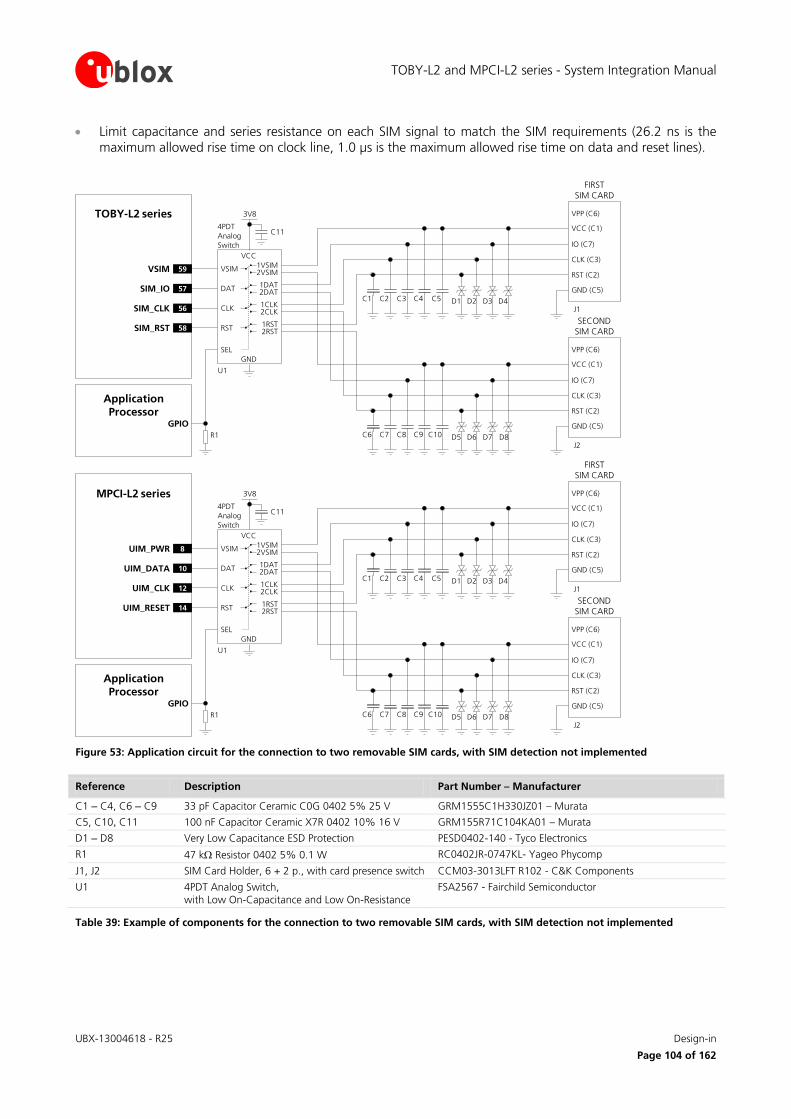
TOBY-L2 and MPCI-L2 series - System Integration Manual
UBX-13004618 - R25 Design-in
Page 104 of 162
Limit capacitance and series resistance on each SIM signal to match the SIM requirements (26.2 ns is the maximum allowed rise time on clock line, 1.0 µs is the maximum allowed rise time on data and reset lines).
TOBY-L2 series
C1
FIRST SIM CARD
VPP (C6)
VCC (C1)
IO (C7)
CLK (C3)
RST (C2)
GND (C5)C2 C3 C5
J1
C4 D1 D2 D3 D4
GND
U1
59VSIM VSIM1VSIM2VSIM
VCC
C114PDT
Analog
Switch
3V8
57SIM_IO DAT 1DAT2DAT
56SIM_CLK CLK 1CLK2CLK
58SIM_RST RST 1RST2RST
SEL
SECOND SIM CARD
VPP (C6)
VCC (C1)
IO (C7)
CLK (C3)
RST (C2)
GND (C5)
J2
C6 C7 C8 C10C9 D5 D6 D7 D8
Application
ProcessorGPIO
R1
MPCI-L2 series
C1
FIRST SIM CARD
VPP (C6)
VCC (C1)
IO (C7)
CLK (C3)
RST (C2)
GND (C5)C2 C3 C5
J1
C4 D1 D2 D3 D4
GND
U1
8UIM_PWR VSIM 1VSIM2VSIM
VCC
C114PDT
Analog
Switch
3V8
10UIM_DATA DAT 1DAT2DAT
12UIM_CLK CLK 1CLK2CLK
14UIM_RESET RST 1RST2RST
SEL
SECOND SIM CARD
VPP (C6)
VCC (C1)
IO (C7)
CLK (C3)
RST (C2)
GND (C5)
J2
C6 C7 C8 C10C9 D5 D6 D7 D8
Application
ProcessorGPIO
R1
Figure 53: Application circuit for the connection to two removable SIM cards, with SIM detection not implemented
Reference Description Part Number – Manufacturer
C1 – C4, C6 – C9 33 pF Capacitor Ceramic C0G 0402 5% 25 V GRM1555C1H330JZ01 – Murata
C5, C10, C11 100 nF Capacitor Ceramic X7R 0402 10% 16 V GRM155R71C104KA01 – Murata
D1 – D8 Very Low Capacitance ESD Protection PESD0402-140 - Tyco Electronics
R1 47 k Resistor 0402 5% 0.1 W RC0402JR-0747KL- Yageo Phycomp
J1, J2 SIM Card Holder, 6 + 2 p., with card presence switch CCM03-3013LFT R102 - C&K Components
U1 4PDT Analog Switch, with Low On-Capacitance and Low On-Resistance
FSA2567 - Fairchild Semiconductor
Table 39: Example of components for the connection to two removable SIM cards, with SIM detection not implemented
TOBY-L2 and MPCI-L2 series - System Integration Manual
UBX-13004618 - R25 Design-in
Page 105 of 162
2.5.2 Guidelines for SIM layout design
The layout of the SIM card interface lines (VSIM, SIM_CLK, SIM_IO, SIM_RST or UIM_PWR, UIM_DATA, UIM_CLK, UIM_RESET) may be critical if the SIM card is placed far away from the TOBY-L2 and MPCI-L2 series modules or in close proximity to the RF antenna: these two cases should be avoided or at least mitigated as described below.
In the first case, the long connection can cause the radiation of some harmonics of the digital data frequency as any other digital interface. It is recommended to keep the traces short and avoid coupling with RF line or sensitive analog inputs.
In the second case, the same harmonics can be picked up and create self-interference that can reduce the sensitivity of LTE/3G/2G receiver channels whose carrier frequency is coincidental with harmonic frequencies. It is strongly recommended to place the RF bypass capacitors suggested in Figure 50 near the SIM connector.
In addition, since the SIM card is typically accessed by the end user, it can be subjected to ESD discharges. Add adequate ESD protection as suggested to protect module SIM pins near the SIM connector.
Limit capacitance and series resistance on each SIM signal to match the SIM specifications. The connections should always be kept as short as possible.
Avoid coupling with any sensitive analog circuit, since the SIM signals can cause the radiation of some harmonics of the digital data frequency.
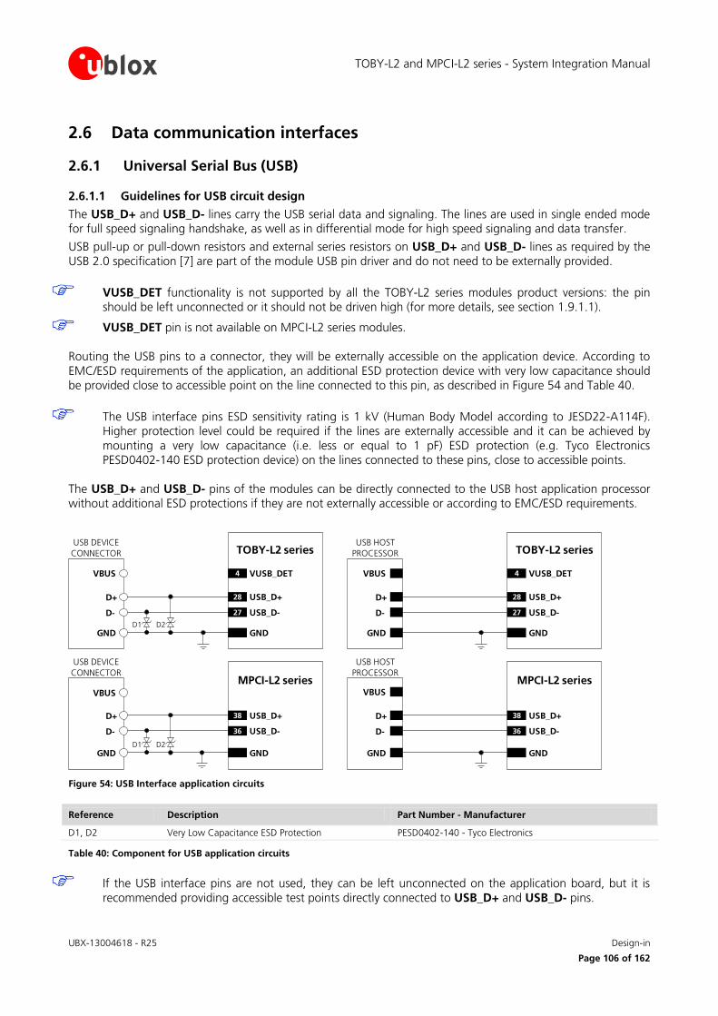
TOBY-L2 and MPCI-L2 series - System Integration Manual
UBX-13004618 - R25 Design-in
Page 106 of 162
2.6 Data communication interfaces
2.6.1 Universal Serial Bus (USB)
2.6.1.1 Guidelines for USB circuit design
The USB_D+ and USB_D- lines carry the USB serial data and signaling. The lines are used in single ended mode for full speed signaling handshake, as well as in differential mode for high speed signaling and data transfer.
USB pull-up or pull-down resistors and external series resistors on USB_D+ and USB_D- lines as required by the USB 2.0 specification [7] are part of the module USB pin driver and do not need to be externally provided.
VUSB_DET functionality is not supported by all the TOBY-L2 series modules product versions: the pin should be left unconnected or it should not be driven high (for more details, see section 1.9.1.1).
VUSB_DET pin is not available on MPCI-L2 series modules.
Routing the USB pins to a connector, they will be externally accessible on the application device. According to EMC/ESD requirements of the application, an additional ESD protection device with very low capacitance should be provided close to accessible point on the line connected to this pin, as described in Figure 54 and Table 40.
The USB interface pins ESD sensitivity rating is 1 kV (Human Body Model according to JESD22-A114F). Higher protection level could be required if the lines are externally accessible and it can be achieved by mounting a very low capacitance (i.e. less or equal to 1 pF) ESD protection (e.g. Tyco Electronics PESD0402-140 ESD protection device) on the lines connected to these pins, close to accessible points.
The USB_D+ and USB_D- pins of the modules can be directly connected to the USB host application processor without additional ESD protections if they are not externally accessible or according to EMC/ESD requirements.
D+
D-
GND
28 USB_D+
27 USB_D-
GND
USB DEVICE
CONNECTOR
VBUS
D+
D-
GND
28 USB_D+
27 USB_D-
GND
USB HOST
PROCESSOR
D+
D-
GND
38 USB_D+
36 USB_D-
GND
USB DEVICE
CONNECTOR
VBUS
TOBY-L2 series TOBY-L2 series
MPCI-L2 series MPCI-L2 series
D+
D-
GND
38 USB_D+
36 USB_D-
GND
USB HOST
PROCESSOR
VBUS 4 VUSB_DET4 VUSB_DET
D1 D2
D1 D2
VBUS
Figure 54: USB Interface application circuits
Reference Description Part Number - Manufacturer
D1, D2 Very Low Capacitance ESD Protection PESD0402-140 - Tyco Electronics
Table 40: Component for USB application circuits
If the USB interface pins are not used, they can be left unconnected on the application board, but it is recommended providing accessible test points directly connected to USB_D+ and USB_D- pins.
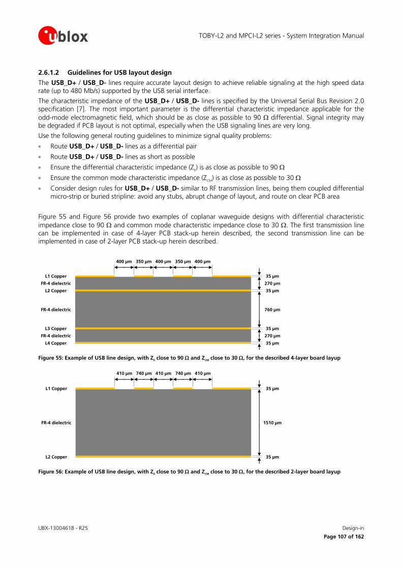
TOBY-L2 and MPCI-L2 series - System Integration Manual
UBX-13004618 - R25 Design-in
Page 107 of 162
2.6.1.2 Guidelines for USB layout design
The USB_D+ / USB_D- lines require accurate layout design to achieve reliable signaling at the high speed data rate (up to 480 Mb/s) supported by the USB serial interface.
The characteristic impedance of the USB_D+ / USB_D- lines is specified by the Universal Serial Bus Revision 2.0 specification [7]. The most important parameter is the differential characteristic impedance applicable for the
odd-mode electromagnetic field, which should be as close as possible to 90 differential. Signal integrity may be degraded if PCB layout is not optimal, especially when the USB signaling lines are very long.
Use the following general routing guidelines to minimize signal quality problems:
Route USB_D+ / USB_D- lines as a differential pair
Route USB_D+ / USB_D- lines as short as possible
Ensure the differential characteristic impedance (Z0) is as close as possible to 90
Ensure the common mode characteristic impedance (ZCM
) is as close as possible to 30
Consider design rules for USB_D+ / USB_D- similar to RF transmission lines, being them coupled differential micro-strip or buried stripline: avoid any stubs, abrupt change of layout, and route on clear PCB area
Figure 55 and Figure 56 provide two examples of coplanar waveguide designs with differential characteristic
impedance close to 90 and common mode characteristic impedance close to 30 . The first transmission line can be implemented in case of 4-layer PCB stack-up herein described, the second transmission line can be implemented in case of 2-layer PCB stack-up herein described.
35 µm
35 µm
35 µm
35 µm
270 µm
270 µm
760 µm
L1 Copper
L3 Copper
L2 Copper
L4 Copper
FR-4 dielectric
FR-4 dielectric
FR-4 dielectric
350 µm 400 µm400 µm350 µm400 µm
Figure 55: Example of USB line design, with Z0 close to 90 and Z
CM close to 30 , for the described 4-layer board layup
35 µm
35 µm
1510 µm
L2 Copper
L1 Copper
FR-4 dielectric
740 µm 410 µm410 µm740 µm410 µm
Figure 56: Example of USB line design, with Z0 close to 90 and Z
CM close to 30 , for the described 2-layer board layup
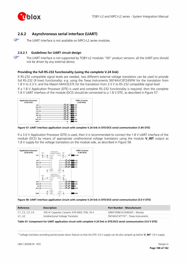
TOBY-L2 and MPCI-L2 series - System Integration Manual
UBX-13004618 - R25 Design-in
Page 108 of 162
2.6.2 Asynchronous serial interface (UART)
The UART interface is not available on MPCI-L2 series modules.
2.6.2.1 Guidelines for UART circuit design
The UART interface is not supported by TOBY-L2 modules “00” product versions: all the UART pins should not be driven by any external device.
Providing the full RS-232 functionality (using the complete V.24 link)
If RS-232 compatible signal levels are needed, two different external voltage translators can be used to provide full RS-232 (9 lines) functionality: e.g. using the Texas Instruments SN74AVC8T245PW for the translation from 1.8 V to 3.3 V, and the Maxim MAX3237E for the translation from 3.3 V to RS-232 compatible signal level.
If a 1.8 V Application Processor (DTE) is used and complete RS-232 functionality is required, then the complete 1.8 V UART interface of the module (DCE) should be connected to a 1.8 V DTE, as described in Figure 57.
TxD
Application Processor(1.8V DTE)
RxD
RTS
CTS
DTR
DSR
RI
DCD
GND
TOBY-L2 series (1.8V DCE)
16 TXD
13 DTR
17 RXD
14 RTS
15 CTS
10 DSR
11 RI
12 DCD
GND
0Ω TP
0Ω TP
0Ω TP
0Ω TP
0Ω TP
0Ω TP
0Ω TP
0Ω TP
Figure 57: UART interface application circuit with complete V.24 link in DTE/DCE serial communication (1.8V DTE)
If a 3.0 V Application Processor (DTE) is used, then it is recommended to connect the 1.8 V UART interface of the module (DCE) by means of appropriate unidirectional voltage translators using the module V_INT output as 1.8 V supply for the voltage translators on the module side, as described in Figure 58.
5 V_INT
TxD
Application Processor(3.0V DTE)
RxD
RTS
CTS
DTR
DSR
RI
DCD
GND
TOBY-L2 series (1.8V DCE)
16 TXD
13 DTR
17 RXD
14 RTS
15 CTS
10 DSR
11 RI
12 DCD
GND
1V8
B1 A1
GND
U1
B3A3
VCCBVCCA
UnidirectionalVoltage Translator
C1 C2
3V0
DIR3
DIR2 OE
DIR1
VCC
B2 A2
B4A4
DIR4
1V8
B1 A1
GND
U2
B3A3
VCCBVCCA
UnidirectionalVoltage Translator
C3 C4
3V0
DIR1
DIR3 OE
B2 A2
B4A4
DIR4
DIR2
TP
0Ω TP
0Ω TP
0Ω TP
0Ω TP
0Ω TP
0Ω TP
0Ω TP
0Ω TP
Figure 58: UART interface application circuit with complete V.24 link in DTE/DCE serial communication (3.0 V DTE)
Reference Description Part Number - Manufacturer
C1, C2, C3, C4 100 nF Capacitor Ceramic X7R 0402 10% 16 V GRM155R61A104KA01 - Murata
U1, U2 Unidirectional Voltage Translator SN74AVC4T77419
- Texas Instruments
Table 41: Component for UART application circuit with complete V.24 link in DTE/DCE serial communication (3.0 V DTE)
19
Voltage translator providing partial power down feature so that the DTE 3.0 V supply can be also ramped up before V_INT 1.8 V supply
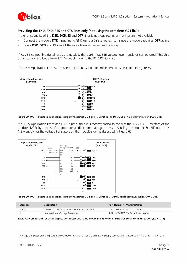
TOBY-L2 and MPCI-L2 series - System Integration Manual
UBX-13004618 - R25 Design-in
Page 109 of 162
Providing the TXD, RXD, RTS and CTS lines only (not using the complete V.24 link)
If the functionality of the DSR, DCD, RI and DTR lines is not required in, or the lines are not available:
Connect the module DTR input line to GND using a 0 series resistor, since the module requires DTR active
Leave DSR, DCD and RI lines of the module unconnected and floating
If RS-232 compatible signal levels are needed, the Maxim 13234E voltage level translator can be used. This chip translates voltage levels from 1.8 V (module side) to the RS-232 standard.
If a 1.8 V Application Processor is used, the circuit should be implemented as described in Figure 59.
TxD
Application Processor(1.8V DTE)
RxD
RTS
CTS
DTR
DSR
RI
DCD
GND
TOBY-L2 series (1.8V DCE)
16 TXD
13 DTR
17 RXD
14 RTS
15 CTS
10 DSR
11 RI
12 DCD
GND
0Ω TP
0Ω TP
0Ω TP
0Ω TP
0Ω TP
TP
TP
TP
Figure 59: UART interface application circuit with partial V.24 link (5-wire) in the DTE/DCE serial communication (1.8V DTE)
If a 3.0 V Application Processor (DTE) is used, then it is recommended to connect the 1.8 V UART interface of the module (DCE) by means of appropriate unidirectional voltage translators using the module V_INT output as 1.8 V supply for the voltage translators on the module side, as described in Figure 60.
5 V_INT
TxD
Application Processor
(3.0V DTE)
RxD
RTS
CTS
DTR
DSR
RI
DCD
GND
TOBY-L2 series
(1.8V DCE)
16 TXD
13 DTR
17 RXD
14 RTS
15 CTS
10 DSR
11 RI
12 DCD
GND
1V8
B1 A1
GND
U1
B3A3
VCCBVCCA
UnidirectionalVoltage Translator
C1 C2
3V0
DIR3
DIR2 OE
DIR1
VCC
B2 A2
B4A4
DIR4
TP
0Ω TP
0Ω TP
0Ω TP
0Ω TP
0Ω TP
TP
TP
TP
Figure 60: UART interface application circuit with partial V.24 link (5-wire) in DTE/DCE serial communication (3.0 V DTE)
Reference Description Part Number - Manufacturer
C1, C2 100 nF Capacitor Ceramic X7R 0402 10% 16 V GRM155R61A104KA01 - Murata
U1 Unidirectional Voltage Translator SN74AVC4T77420
- Texas Instruments
Table 42: Component for UART application circuit with partial V.24 link (5-wire) in DTE/DCE serial communication (3.0 V DTE)
20
Voltage translator providing partial power down feature so that the DTE 3.0 V supply can be also ramped up before V_INT 1.8 V supply
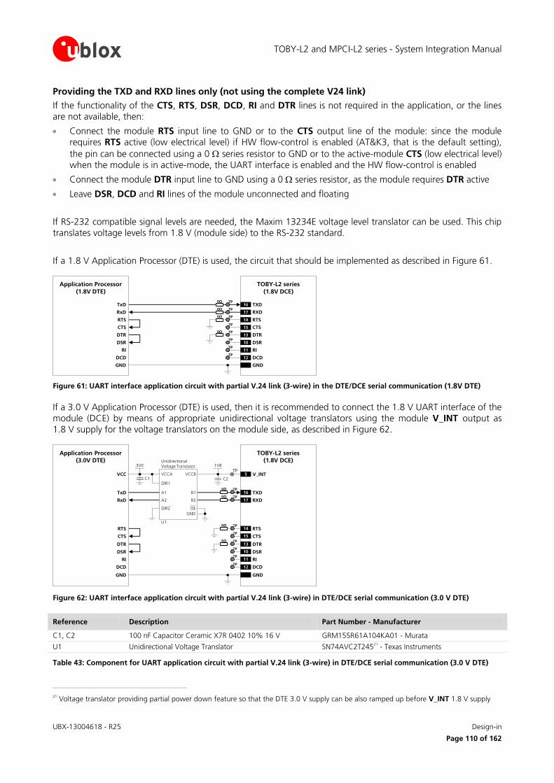
TOBY-L2 and MPCI-L2 series - System Integration Manual
UBX-13004618 - R25 Design-in
Page 110 of 162
Providing the TXD and RXD lines only (not using the complete V24 link)
If the functionality of the CTS, RTS, DSR, DCD, RI and DTR lines is not required in the application, or the lines are not available, then:
Connect the module RTS input line to GND or to the CTS output line of the module: since the module requires RTS active (low electrical level) if HW flow-control is enabled (AT&K3, that is the default setting),
the pin can be connected using a 0 series resistor to GND or to the active-module CTS (low electrical level) when the module is in active-mode, the UART interface is enabled and the HW flow-control is enabled
Connect the module DTR input line to GND using a 0 series resistor, as the module requires DTR active
Leave DSR, DCD and RI lines of the module unconnected and floating
If RS-232 compatible signal levels are needed, the Maxim 13234E voltage level translator can be used. This chip translates voltage levels from 1.8 V (module side) to the RS-232 standard.
If a 1.8 V Application Processor (DTE) is used, the circuit that should be implemented as described in Figure 61.
TxD
Application Processor
(1.8V DTE)
RxD
RTS
CTS
DTR
DSR
RI
DCD
GND
TOBY-L2 series
(1.8V DCE)
16 TXD
13 DTR
17 RXD
14 RTS
15 CTS
10 DSR
11 RI
12 DCD
GND
0Ω TP
0Ω TP
0Ω TP
TP
0Ω TP
TP
TP
TP
Figure 61: UART interface application circuit with partial V.24 link (3-wire) in the DTE/DCE serial communication (1.8V DTE)
If a 3.0 V Application Processor (DTE) is used, then it is recommended to connect the 1.8 V UART interface of the module (DCE) by means of appropriate unidirectional voltage translators using the module V_INT output as 1.8 V supply for the voltage translators on the module side, as described in Figure 62.
5 V_INT
TxD
Application Processor
(3.0V DTE)
RxD
DTR
DSR
RI
DCD
GND
TOBY-L2 series
(1.8V DCE)
16 TXD
13 DTR
17 RXD
10 DSR
11 RI
12 DCD
GND
1V8
B1 A1
GND
U1
VCCBVCCA
Unidirectional
Voltage Translator
C1 C2
3V0
DIR1
DIR2 OE
VCC
B2 A2
RTS
CTS
14 RTS
15 CTS
TP
0Ω TP
0Ω TP
0Ω TP
TP
0Ω TP
TP
TP
TP
Figure 62: UART interface application circuit with partial V.24 link (3-wire) in DTE/DCE serial communication (3.0 V DTE)
Reference Description Part Number - Manufacturer
C1, C2 100 nF Capacitor Ceramic X7R 0402 10% 16 V GRM155R61A104KA01 - Murata
U1 Unidirectional Voltage Translator SN74AVC2T24521
- Texas Instruments
Table 43: Component for UART application circuit with partial V.24 link (3-wire) in DTE/DCE serial communication (3.0 V DTE)
21
Voltage translator providing partial power down feature so that the DTE 3.0 V supply can be also ramped up before V_INT 1.8 V supply
TOBY-L2 and MPCI-L2 series - System Integration Manual
UBX-13004618 - R25 Design-in
Page 111 of 162
Additional considerations
If a 3.0 V Application Processor (DTE) is used, the voltage scaling from any 3.0 V output of the DTE to the corresponding 1.8 V input of the module (DCE) can be implemented as an alternative low-cost solution, by means of an appropriate voltage divider. Consider the value of the pull-up integrated at the input of the module (DCE) for the correct selection of the voltage divider resistance values and mind that any DTE signal connected to the module must be tri-stated or set low when the module is in power-down mode and during the module power-on sequence (at least until the activation of the V_INT supply output of the module), to avoid latch-up of circuits and allow a proper boot of the module (see the remark below).
Moreover, the voltage scaling from any 1.8 V output of the cellular module (DCE) to the corresponding 3.0 V input of the Application Processor (DTE) can be implemented by means of an appropriate low-cost non-inverting buffer with open drain output. The non-inverting buffer should be supplied by the V_INT supply output of the cellular module. Consider the value of the pull-up integrated at each input of the DTE (if any) and the baud rate required by the application for the appropriate selection of the resistance value for the external pull-up biased by the application processor supply rail.
If power saving is enabled the application circuit with the TXD and RXD lines only is not recommended. During command mode the DTE must send to the module a wake-up character or a dummy “AT” before each command line (see section 1.9.2.4 for the complete description), but during data mode the wake-up character or the dummy “AT” would affect the data communication.
Do not apply voltage to any UART interface pin before the switch-on of the UART supply source (V_INT), to avoid latch-up of circuits and allow a proper boot of the module. If the external signals connected to the cellular module cannot be tri-stated or set low, insert a multi channel digital switch (e.g. TI SN74CB3Q16244, TS5A3159, or TS5A63157) between the two-circuit connections and set to high impedance before V_INT switch-on.
ESD sensitivity rating of UART interface pins is 1 kV (Human Body Model according to JESD22-A114). Higher protection level could be required if the lines are externally accessible and it can be achieved by mounting an ESD protection (e.g. EPCOS CA05P4S14THSG varistor array) close to accessible points.
If the UART interface pins are not used, they can be left unconnected on the application board, but it is recommended providing accessible test points directly connected to all the UART pins (TXD, RXD, RTS,
CTS, DTR, DSR, DCD, RI) for diagnostic purpose, in particular providing a 0 series jumper on each line to detach each UART pin of the module from the DTE application processor.
2.6.2.2 Guidelines for UART layout design
The UART serial interface requires the same consideration regarding electro-magnetic interference as any other digital interface. Keep the traces short and avoid coupling with RF line or sensitive analog inputs, since the signals can cause the radiation of some harmonics of the digital data frequency.
TOBY-L2 and MPCI-L2 series - System Integration Manual
UBX-13004618 - R25 Design-in
Page 112 of 162
2.6.3 DDC (I2C) interface
The I2C bus compatible Display Data Channel interface is not available on MPCI-L2 series modules.
2.6.3.1 Guidelines for DDC (I2C) circuit design
I2C bus function is not supported by TOBY-L2 series modules “00”, “01”, “60” and TOBY-L201-02S
product versions: the pins should not be driven by any external device.
The DDC I2C-bus master interface can be used to communicate with external I
2C-bus slaves as an audio codec.
Beside the general considerations reported below, see the section 2.7.1 for an application circuit example with an external audio codec I
2C-bus slave.
To be compliant with the I2C bus specifications, the module bus interface pads are open drain output and pull up
resistors must be mounted externally. Resistor values must conform to I2C bus specifications [13]: for example,
4.7 k resistors can be commonly used. Pull-ups must be connected to a supply voltage of 1.8 V (typical), since this is the voltage domain of the DDC pins which are not tolerant to higher voltage values (e.g. 3.0 V).
Connect the DDC (I2C) pull-ups to the V_INT 1.8 V supply source, or another 1.8 V supply source enabled
after V_INT, as any external signal connected to the DDC (I2C) interface must not be set high before the
switch-on of the V_INT supply of DDC (I2C) pins, to avoid latch-up of circuits and let a proper boot of the
module.
The signal shape is defined by the values of the pull-up resistors and the bus capacitance. Long wires on the bus will increase the capacitance. If the bus capacitance is increased, use pull-up resistors with nominal resistance
value lower than 4.7 k, to match the I2C bus specifications [13] regarding rise and fall times of the signals.
Capacitance and series resistance must be limited on the bus to match the I2C specifications (1.0 µs is the
maximum allowed rise time on the SCL and SDA lines): route connections as short as possible.
If the pins are not used as DDC bus interface, they can be left unconnected.
ESD sensitivity rating of the DDC (I2C) pins is 1 kV (Human Body Model according to JESD22-A114).
Higher protection level could be required if the lines are externally accessible and it can be achieved by mounting an ESD protection (e.g. EPCOS CA05P4S14THSG varistor array) close to accessible points.
2.6.3.2 Guidelines for DDC (I2C) layout design
The DDC (I2C) serial interface requires the same consideration regarding electro-magnetic interference as any
other digital interface. Keep the traces short and avoid coupling with RF line or sensitive analog inputs, since the signals can cause the radiation of some harmonics of the digital data frequency.
TOBY-L2 and MPCI-L2 series - System Integration Manual
UBX-13004618 - R25 Design-in
Page 113 of 162
2.6.4 Secure Digital Input Output interface (SDIO)
The SDIO Secure Digital Input Output interface is not available on MPCI-L2 series modules.
2.6.4.1 Guidelines for SDIO circuit design
The functionality of the SDIO Secure Digital Input Output interface pins is not supported by TOBY-L2 modules “00”, “01” and “60” product versions: the pins should not be driven by any external device.
TOBY-L2 series modules include a 4-bit Secure Digital Input Output interface (SDIO_D0, SDIO_D1, SDIO_D2, SDIO_D3, SDIO_CLK, SDIO_CMD) designed to communicate with an external u-blox short range Wi-Fi module.
Combining a u-blox cellular module with a u-blox short range communication module gives designers full access to the Wi-Fi module directly via the cellular module, so that a second interface connected to the Wi-Fi module is not necessary. AT commands via the AT interfaces of the cellular module (UART, USB) allows full control of the Wi-Fi module from any host processor, because Wi-Fi control messages are relayed to the Wi-Fi module via the dedicated SDIO interface (for more details, see the Wi-Fi AT commands in the u-blox AT Commands Manual [3] and see the Wi-Fi / Cellular Integration Application Note [15]).
Figure 63 and Table 44 show an application circuit for connecting TOBY-L2 series cellular modules (except “00”, “01” and “60” product versions) to u-blox ELLA-W131 short range Wi-Fi 802.11 b/g/n modules:
The SDIO pins of the cellular module are connected to the related SDIO pins of the u-blox ELLA-W1 series short range Wi-Fi module, with appropriate low value series damping resistors to avoid reflections and other losses in signal integrity, which may create ringing and loss of a square wave shape.
The most appropriate value for the series damping resistors on the SDIO lines depends on the specific line lengths and layout implemented. In general, the SDIO series resistors are not strictly required, but it is
recommended to slow the SDIO signal, for example with 22 or 33 resistors, and avoid any possible ringing problem without violating the rise / fall time requirements.
The V_INT supply output pin of the cellular module is connected to the shutdown input pin (SHDNn) of the two LDO regulators providing the 3.3 V and 1.8 V supply rails for the u-blox ELLA-W1 series Wi-Fi module, with appropriate pull-down resistors to avoid an improper switch on of the Wi-Fi module before the switch-on of the V_INT supply source of the cellular module SDIO interface pins.
The GPIO1 pin of the cellular module is connected to the active low full power down input pin (PDn) of the u-blox ELLA-W1 series Wi-Fi module, implementing the Wi-Fi enable function.
The configuration pin (CFG) of the u-blox ELLA-W1 series Wi-Fi module is connected to ground by means of a proper pull-down resistor for operation without sleep clock
The sleep clock input pin (SLEEP_CLK) of the u-blox ELLA-W1 series Wi-Fi module is left not connected, because an external clock source is not required.
The WLAN LED open drain output pin (LED_0) of the u-blox ELLA-W1 series Wi-Fi module is connected to an LED with appropriate current limiting resistor, indicating Wi-Fi activity as additional optional feature.
The WLAN antenna RF input/output (ANT1) of the u-blox ELLA-W131 Wi-Fi module is connected to a Wi-Fi antenna with an appropriate series Wi-Fi 2.4 GHz band-pass filter specifically designed for the coexistence between the Wi-Fi 2.4 GHz RF signals (2402...2482 MHz) and the LTE band 7 RF signals (2500...2690 MHz), as for example the Wi-Fi BAW 2.4 GHz band-pass filter TDK EPCOS B9604, or the TriQuint 885071, or the TriQuint 885032 or the Avago ACPF-7424, or the Taiyo Yuden F6HF2G441AF46.
All GND pins of the cellular module and the u-blox ELLA-W1 series Wi-Fi module are connected to ground.
All the other pins of the u-blox ELLA-W1 series Wi-Fi module are intended to be not connected.
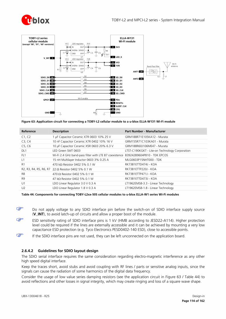
TOBY-L2 and MPCI-L2 series - System Integration Manual
UBX-13004618 - R25 Design-in
Page 114 of 162
R2
LDO regulator
ELLA-W131
Wi-Fi module3V3VCC
U1
C1
R1
Wi-Fi enable
SD_D015
SD_D116
SD_D211
SD_D312
SD_CLK14
SD_CMD13
PDn9
OUTIN
SENSE
BYP
SHDNn
GND
TOBY-L2 series
cellular module(except ‘00’, ’01’, ’60’ versions)
SDIO_D0 66
SDIO_D1 68
SDIO_D2 63
SDIO_D3 67
SDIO_CLK 64
SDIO_CMD 65
V_INT 5
GPIO1 21
C3
3V34
C5
LDO regulator 1V8VCC
U2
C2
OUTIN
SENSE
BYP
SHDNn
GND C4
VIO5
C6
1V86
R3
R4
R5
R6
R7
RESETn10
SLEEP_CLK19
CFG20
LED_02
R9 GND
ANT1 29
ANT2 26
R8
DL1
GND
Band-Pass filter
L1
Wi-Fi antenna
FL1
Figure 63: Application circuit for connecting a TOBY-L2 cellular module to a u-blox ELLA-W131 Wi-Fi module
Reference Description Part Number - Manufacturer
C1, C2 1 µF Capacitor Ceramic X7R 0603 10% 25 V GRM188R71E105KA12 - Murata
C3, C4 10 nF Capacitor Ceramic X7R 0402 10% 16 V GRM155R71C103KA01 - Murata
C5, C6 10 µF Capacitor Ceramic X5R 0603 20% 6.3 V GRM188R60J106ME47 - Murata
DL1 LED Green SMT 0603 LTST-C190KGKT - Lite-on Technology Corporation
FL1 Wi-Fi 2.4 GHz band-pass filter with LTE B7 coexistence B39242B9604P810 - TDK EPCOS
L1 15 nH Multilayer Inductor 0603 3% 0.25 A MLG0603P15NHT000 - TDK
R1 470 k Resistor 0402 5% 0.1 W RK73B1ETTD474J - KOA
R2, R3, R4, R5, R6, R7 22 Resistor 0402 5% 0.1 W RK73B1ETTP220J - KOA
R8 470 Resistor 0402 5% 0.1 W RK73B1ETTP471J - KOA
R9 47 k Resistor 0402 5% 0.1 W RK73B1ETTD473J - KOA
U1 LDO Linear Regulator 3.0 V 0.3 A LT1962EMS8-3.3 - Linear Technology
U2 LDO Linear Regulator 1.8 V 0.3 A LT1962EMS8-1.8 - Linear Technology
Table 44: Components for connecting TOBY-L2xx-50S cellular modules to u-blox ELLA-W1 series Wi-Fi modules
Do not apply voltage to any SDIO interface pin before the switch-on of SDIO interface supply source (V_INT), to avoid latch-up of circuits and allow a proper boot of the module.
ESD sensitivity rating of SDIO interface pins is 1 kV (HMB according to JESD22-A114). Higher protection level could be required if the lines are externally accessible and it can be achieved by mounting a very low capacitance ESD protection (e.g. Tyco Electronics PESD0402-140 ESD), close to accessible points.
If the SDIO interface pins are not used, they can be left unconnected on the application board.
2.6.4.2 Guidelines for SDIO layout design
The SDIO serial interface requires the same consideration regarding electro-magnetic interference as any other high speed digital interface.
Keep the traces short, avoid stubs and avoid coupling with RF lines / parts or sensitive analog inputs, since the signals can cause the radiation of some harmonics of the digital data frequency.
Consider the usage of low value series damping resistors (see the application circuit in Figure 63 / Table 44) to avoid reflections and other losses in signal integrity, which may create ringing and loss of a square wave shape.
TOBY-L2 and MPCI-L2 series - System Integration Manual
UBX-13004618 - R25 Design-in
Page 115 of 162
2.7 Audio interface
2.7.1 Digital audio interface
The I2S interface is not available on MPCI-L2 series modules.
2.7.1.1 Guidelines for digital audio circuit design
The I2S interface is not supported by TOBY-L2 series modules “00”, “01”, “60”, TOBY-L201-02S and
TOBY-L220-62S product versions: the pins should not be driven by any external device.
I2S digital audio interface can be connected to an external digital audio device for voice applications.
Any external digital audio device compliant with the configuration of the digital audio interface of the TOBY-L2 cellular module can be used, given that the external digital audio device must provide:
The slave role: opposite role of TOBY-L2 modules, which act as master only
The same mode and frame format: PCM / short synch mode or Normal I2S / long synch mode with
o data in 2’s complement notation
o MSB transmitted first
o data word length = 16-bit (16 clock cycles)
o frame length = synch signal period = 32-bit (32 clock cycles)
The same sample rate, i.e. synch signal frequency, configurable by AT+UI2S <I2S_sample_rate> parameter
o 8 kHz
o 16 kHz
The same serial clock frequency:
o 32 x <I2S_sample_rate>
Compatible voltage levels (1.80 V typ.), otherwise it is recommended to connect the 1.8 V digital audio interface of the module to the external 3.0 V (or similar) digital audio device by means of appropriate unidirectional voltage translators (e.g. TI SN74AVC4T774 or SN74AVC2T245, providing partial power down feature so that the digital audio device 3.0 V supply can be also ramped up before V_INT 1.8 V supply), using the module V_INT output as 1.8 V supply for the voltage translators on the module side
Support of the side-tone, which is not available in the internal audio processing system of TOBY-L2 modules as summarized in Figure 26. The side-tone is a part of the user's speech on uplink path that should be listened on downlink path by the user himself to have perception the call is on.
For the appropriate selection of a compliant external digital audio device, see section 1.10.1 and see the +UI2S AT command description in the u-blox AT Commands Manual [3] for further details regarding the capabilities and the possible settings of I
2S digital audio interface of TOBY-L2 modules.
An appropriate specific application circuit has to be implemented and configured according to the particular external digital audio device or audio codec used and according to the application requirements.
Examples of manufacturers offering compatible audio codec parts are the following:
Maxim Integrated (as the MAX9860, MAX9867, MAX9880A audio codecs)
Texas Instruments / National Semiconductor
Cirrus Logic / Wolfson Microelectronics
Nuvoton Technology
Asahi Kasei Microdevices
Realtek Semiconductor
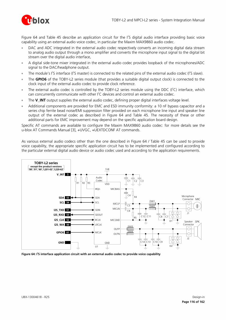
TOBY-L2 and MPCI-L2 series - System Integration Manual
UBX-13004618 - R25 Design-in
Page 116 of 162
Figure 64 and Table 45 describe an application circuit for the I2S digital audio interface providing basic voice
capability using an external audio voice codec, in particular the Maxim MAX9860 audio codec.
DAC and ADC integrated in the external audio codec respectively converts an incoming digital data stream to analog audio output through a mono amplifier and converts the microphone input signal to the digital bit stream over the digital audio interface,
A digital side-tone mixer integrated in the external audio codec provides loopback of the microphones/ADC signal to the DAC/headphone output.
The module’s I2S interface (I
2S master) is connected to the related pins of the external audio codec (I
2S slave).
The GPIO6 of the TOBY-L2 series module (that provides a suitable digital output clock) is connected to the clock input of the external audio codec to provide clock reference.
The external audio codec is controlled by the TOBY-L2 series module using the DDC (I2C) interface, which
can concurrently communicate with other I2C devices and control an external audio codec.
The V_INT output supplies the external audio codec, defining proper digital interfaces voltage level.
Additional components are provided for EMC and ESD immunity conformity: a 10 nF bypass capacitor and a series chip ferrite bead noise/EMI suppression filter provided on each microphone line input and speaker line output of the external codec as described in Figure 64 and Table 45. The necessity of these or other additional parts for EMC improvement may depend on the specific application board design.
Specific AT commands are available to configure the Maxim MAX9860 audio codec: for more details see the u-blox AT Commands Manual [3], +UVGC, +UEXTDCONF AT commands.
As various external audio codecs other than the one described in Figure 64 / Table 45 can be used to provide voice capability, the appropriate specific application circuit has to be implemented and configured according to the particular external digital audio device or audio codec used and according to the application requirements.
TOBY-L2 seriesexcept the product versions
‘00’,‘01’,‘60’,‘L201-02’,’L220-62’
R2R1
BCLK
GND
U1
LRCLK
Audio
Codec
SDIN
SDOUT
SDA
SCL
MCLK
IRQn
R3C3C2C1
VDD
1V8
MICBIAS
C4R4
C5
C6MICLN
MICLP
D1
Microphone Connector MIC
C12 C11
J1
MICGNDR5 C8 C7
D2
SPKSpeaker Connector
OUTP
OUTN
J2
C10 C9C14 C13
EMI3
EMI4
EMI1
EMI2
GPIO6
55SDA
54SCL
61
GND
5V_INT
52I2S_CLK
50I2S_WA
51I2S_TXD
53I2S_RXD
Figure 64: I2S interface application circuit with an external audio codec to provide voice capability
TOBY-L2 and MPCI-L2 series - System Integration Manual
UBX-13004618 - R25 Design-in
Page 117 of 162
Reference Description Part Number – Manufacturer
C1 100 nF Capacitor Ceramic X5R 0402 10% 10V GRM155R71C104KA01 – Murata
C2, C4, C5, C6 1 µF Capacitor Ceramic X5R 0402 10% 6.3 V GRM155R60J105KE19 – Murata
C3 10 µF Capacitor Ceramic X5R 0603 20% 6.3 V GRM188R60J106ME47 – Murata
C7, C8, C9, C10 27 pF Capacitor Ceramic COG 0402 5% 25 V GRM1555C1H270JZ01 – Murata
C11, C12, C13, C14 10 nF Capacitor Ceramic X5R 0402 10% 50V GRM155R71C103KA88 – Murata
D1, D2 Low Capacitance ESD Protection USB0002RP or USB0002DP – AVX
EMI1, EMI2, EMI3, EMI4
Chip Ferrite Bead Noise/EMI Suppression Filter 1800 Ohm at 100 MHz, 2700 Ohm at 1 GHz
BLM15HD182SN1 – Murata
J1 Microphone Connector Various manufacturers
J2 Speaker Connector Various manufacturers
MIC 2.2 k Electret Microphone Various manufacturers
R1, R2 4.7 k Resistor 0402 5% 0.1 W RC0402JR-074K7L - Yageo Phycomp
R3 10 k Resistor 0402 5% 0.1 W RC0402JR-0710KL - Yageo Phycomp
R4, R5 2.2 k Resistor 0402 5% 0.1 W RC0402JR-072K2L – Yageo Phycomp
SPK 32 Speaker Various manufacturers
U1 16-Bit Mono Audio Voice Codec MAX9860ETG+ - Maxim
Table 45: Example of components for audio voice codec application circuit
Do not apply voltage to any I2S pin before the switch-on of I
2S supply source (V_INT), to avoid latch-up of
circuits and allow a proper boot of the module. If the external signals connected to the cellular module cannot be tri-stated or set low, insert a multi channel digital switch (e.g. TI SN74CB3Q16244, TS5A3159, or TS5A63157) between the two-circuit connections and set to high impedance before V_INT switch-on.
ESD sensitivity rating of I2S interface pins is 1 kV (Human Body Model according to JESD22-A114). Higher
protection level could be required if the lines are externally accessible and it can be achieved by mounting a general purpose ESD protection (e.g. EPCOS CA05P4S14THSG varistor array) close to accessible points.
If the I2S digital audio pins are not used, they can be left unconnected on the application board.
2.7.1.2 Guidelines for digital audio layout design
I2S interface and clock output lines require the same consideration regarding electro-magnetic interference as
any other high speed digital interface. Keep the traces short and avoid coupling with RF lines / parts or sensitive analog inputs, since the signals can cause the radiation of some harmonics of the digital data frequency.
2.7.1.3 Guidelines for analog audio layout design
Accurate design of the analog audio circuit is very important to obtain clear and high quality audio. The GSM signal burst has a repetition rate of 217 Hz that lies in the audible range. A careful layout is required to reduce the risk of noise from audio lines due to both VCC burst noise coupling and RF detection.
General guidelines for the uplink path (microphone), which is commonly the most sensitive, are the following:
Avoid coupling of any noisy signal to microphone lines: it is strongly recommended to route microphone lines away from module VCC supply line, any switching regulator line, RF antenna lines, digital lines and any other possible noise source.
Avoid coupling between microphone and speaker / receiver lines.
Optimize the mechanical design of the application device, the position, orientation and mechanical fixing (for example, using rubber gaskets) of microphone and speaker parts in order to avoid echo interference between uplink path and downlink path.
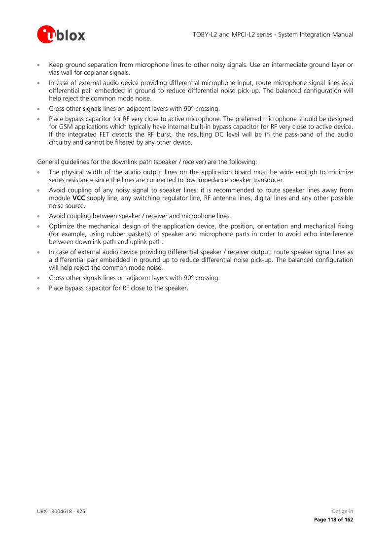
TOBY-L2 and MPCI-L2 series - System Integration Manual
UBX-13004618 - R25 Design-in
Page 118 of 162
Keep ground separation from microphone lines to other noisy signals. Use an intermediate ground layer or vias wall for coplanar signals.
In case of external audio device providing differential microphone input, route microphone signal lines as a differential pair embedded in ground to reduce differential noise pick-up. The balanced configuration will help reject the common mode noise.
Cross other signals lines on adjacent layers with 90° crossing.
Place bypass capacitor for RF very close to active microphone. The preferred microphone should be designed for GSM applications which typically have internal built-in bypass capacitor for RF very close to active device. If the integrated FET detects the RF burst, the resulting DC level will be in the pass-band of the audio circuitry and cannot be filtered by any other device.
General guidelines for the downlink path (speaker / receiver) are the following:
The physical width of the audio output lines on the application board must be wide enough to minimize series resistance since the lines are connected to low impedance speaker transducer.
Avoid coupling of any noisy signal to speaker lines: it is recommended to route speaker lines away from module VCC supply line, any switching regulator line, RF antenna lines, digital lines and any other possible noise source.
Avoid coupling between speaker / receiver and microphone lines.
Optimize the mechanical design of the application device, the position, orientation and mechanical fixing (for example, using rubber gaskets) of speaker and microphone parts in order to avoid echo interference between downlink path and uplink path.
In case of external audio device providing differential speaker / receiver output, route speaker signal lines as a differential pair embedded in ground up to reduce differential noise pick-up. The balanced configuration will help reject the common mode noise.
Cross other signals lines on adjacent layers with 90° crossing.
Place bypass capacitor for RF close to the speaker.
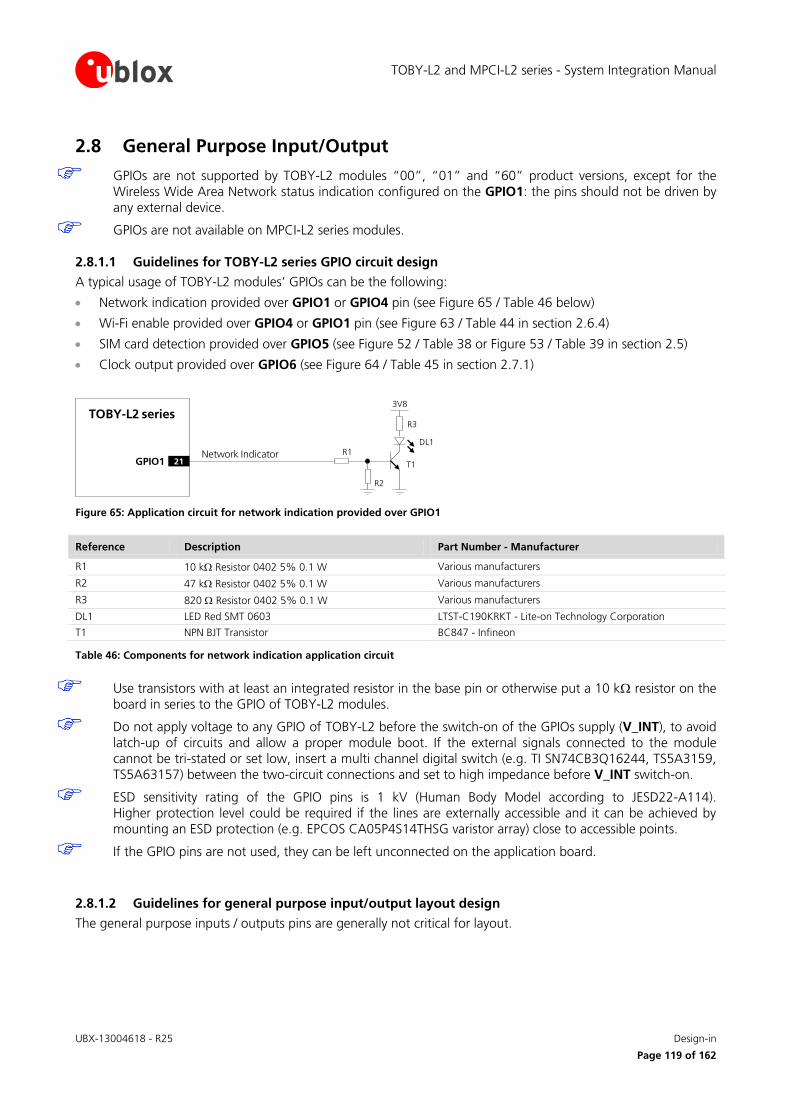
TOBY-L2 and MPCI-L2 series - System Integration Manual
UBX-13004618 - R25 Design-in
Page 119 of 162
2.8 General Purpose Input/Output
GPIOs are not supported by TOBY-L2 modules “00”, “01” and “60” product versions, except for the Wireless Wide Area Network status indication configured on the GPIO1: the pins should not be driven by any external device.
GPIOs are not available on MPCI-L2 series modules.
2.8.1.1 Guidelines for TOBY-L2 series GPIO circuit design
A typical usage of TOBY-L2 modules’ GPIOs can be the following:
Network indication provided over GPIO1 or GPIO4 pin (see Figure 65 / Table 46 below)
Wi-Fi enable provided over GPIO4 or GPIO1 pin (see Figure 63 / Table 44 in section 2.6.4)
SIM card detection provided over GPIO5 (see Figure 52 / Table 38 or Figure 53 / Table 39 in section 2.5)
Clock output provided over GPIO6 (see Figure 64 / Table 45 in section 2.7.1)
TOBY-L2 series
GPIO1R1
R3
3V8
Network Indicator
R2
21
DL1
T1
Figure 65: Application circuit for network indication provided over GPIO1
Reference Description Part Number - Manufacturer
R1 10 k Resistor 0402 5% 0.1 W Various manufacturers
R2 47 k Resistor 0402 5% 0.1 W Various manufacturers
R3 820 Resistor 0402 5% 0.1 W Various manufacturers
DL1 LED Red SMT 0603 LTST-C190KRKT - Lite-on Technology Corporation
T1 NPN BJT Transistor BC847 - Infineon
Table 46: Components for network indication application circuit
Use transistors with at least an integrated resistor in the base pin or otherwise put a 10 k resistor on the board in series to the GPIO of TOBY-L2 modules.
Do not apply voltage to any GPIO of TOBY-L2 before the switch-on of the GPIOs supply (V_INT), to avoid latch-up of circuits and allow a proper module boot. If the external signals connected to the module cannot be tri-stated or set low, insert a multi channel digital switch (e.g. TI SN74CB3Q16244, TS5A3159, TS5A63157) between the two-circuit connections and set to high impedance before V_INT switch-on.
ESD sensitivity rating of the GPIO pins is 1 kV (Human Body Model according to JESD22-A114). Higher protection level could be required if the lines are externally accessible and it can be achieved by mounting an ESD protection (e.g. EPCOS CA05P4S14THSG varistor array) close to accessible points.
If the GPIO pins are not used, they can be left unconnected on the application board.
2.8.1.2 Guidelines for general purpose input/output layout design
The general purpose inputs / outputs pins are generally not critical for layout.

TOBY-L2 and MPCI-L2 series - System Integration Manual
UBX-13004618 - R25 Design-in
Page 120 of 162
2.9 Mini PCIe specific signals (W_DISABLE#, LED_WWAN#)
Mini PCI Express specific signals (W_DISABLE#, LED_WWAN#) are not available on TOBY-L2 series.
2.9.1.1 Guidelines for W_DISABLE# circuit design
As described in Figure 66, the MPCI-L2 series modules W_DISABLE# wireless disable input is equipped with an internal pull-up to the 3.3Vaux supply: an external pull-up resistor is not required and should not be provided.
If connecting the W_DISABLE# input to a push button, the pin will be externally accessible on the application device. According to EMC/ESD requirements of the application, an additional ESD protection device should be provided close to accessible point, as described in Figure 66 and Table 47.
ESD sensitivity rating of the W_DISABLE# pin is 1 kV (HBM according to JESD22-A114). Higher protection level can be required if the line is externally accessible on the application board, e.g. if an accessible push button is directly connected to the W_DISABLE# pin, and it can be achieved by mounting an ESD protection (e.g. EPCOS CA05P4S14THSG varistor) close to accessible point.
An open drain output is suitable to drive the W_DISABLE# input from an application processor as it is equipped with an internal pull-up to the 3.3Vaux supply as described in Figure 66.
A compatible push-pull output of an application processor can also be used. In any case, take care to set the proper level in all the possible scenarios to avoid an inappropriate disabling of the radio operations.
MPCI-L2 series
3.3Vaux
20 W_DISABLE#
Power-on
push button
ESD
Open
Drain Output
Application Processor
MPCI-L2 series
3.3Vaux
20 W_DISABLE#TP TP
22 k 22 k
Figure 66: W_DISABLE# application circuit using a push button and an open drain output of an application processor
Reference Description Remarks
ESD Varistor for ESD protection CT0402S14AHSG - EPCOS
Table 47: Example of ESD protection component for the W_DISABLE# application circuit
If the W_DISABLE# functionality is not required by the application, the pin can be left unconnected.
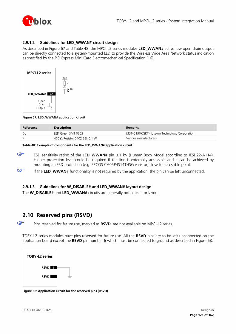
TOBY-L2 and MPCI-L2 series - System Integration Manual
UBX-13004618 - R25 Design-in
Page 121 of 162
2.9.1.2 Guidelines for LED_WWAN# circuit design
As described in Figure 67 and Table 48, the MPCI-L2 series modules LED_WWAN# active-low open drain output can be directly connected to a system-mounted LED to provide the Wireless Wide Area Network status indication as specified by the PCI Express Mini Card Electromechanical Specification [16].
Open
Drain
Output
R
3V3
DL
42LED_WWAN#
MPCI-L2 series
Figure 67: LED_WWAN# application circuit
Reference Description Remarks
DL LED Green SMT 0603 LTST-C190KGKT - Lite-on Technology Corporation
R 470 Resistor 0402 5% 0.1 W Various manufacturers
Table 48: Example of components for the LED_WWAN# application circuit
ESD sensitivity rating of the LED_WWAN# pin is 1 kV (Human Body Model according to JESD22-A114). Higher protection level could be required if the line is externally accessible and it can be achieved by mounting an ESD protection (e.g. EPCOS CA05P4S14THSG varistor) close to accessible point.
If the LED_WWAN# functionality is not required by the application, the pin can be left unconnected.
2.9.1.3 Guidelines for W_DISABLE# and LED_WWAN# layout design
The W_DISABLE# and LED_WWAN# circuits are generally not critical for layout.
2.10 Reserved pins (RSVD)
Pins reserved for future use, marked as RSVD, are not available on MPCI-L2 series.
TOBY-L2 series modules have pins reserved for future use. All the RSVD pins are to be left unconnected on the application board except the RSVD pin number 6 which must be connected to ground as described in Figure 68.
TOBY-L2 series
RSVD
6RSVD
Figure 68: Application circuit for the reserved pins (RSVD)
TOBY-L2 and MPCI-L2 series - System Integration Manual
UBX-13004618 - R25 Design-in
Page 122 of 162
2.11 Module placement
An optimized placement allows a minimum RF line’s length and closer path from DC source for VCC / 3.3Vaux.
Make sure that the module, analog parts and RF circuits are clearly separated from any possible source of radiated energy. In particular, digital circuits can radiate digital frequency harmonics, which can produce Electro-Magnetic Interference that affects the module, analog parts and RF circuits’ performance. Implement proper countermeasures to avoid any possible Electro-Magnetic Compatibility issue.
Make sure that the module, RF and analog parts / circuits, and high speed digital circuits are clearly separated from any sensitive part / circuit which may be affected by Electro-Magnetic Interference, or employ countermeasures to avoid any possible Electro-Magnetic Compatibility issue.
Provide enough clearance between the module and any external part.
The heat dissipation during continuous transmission at maximum power can significantly raise the temperature of the application base-board below the TOBY-L2 and MPCI-L2 series modules: avoid placing temperature sensitive devices close to the module.
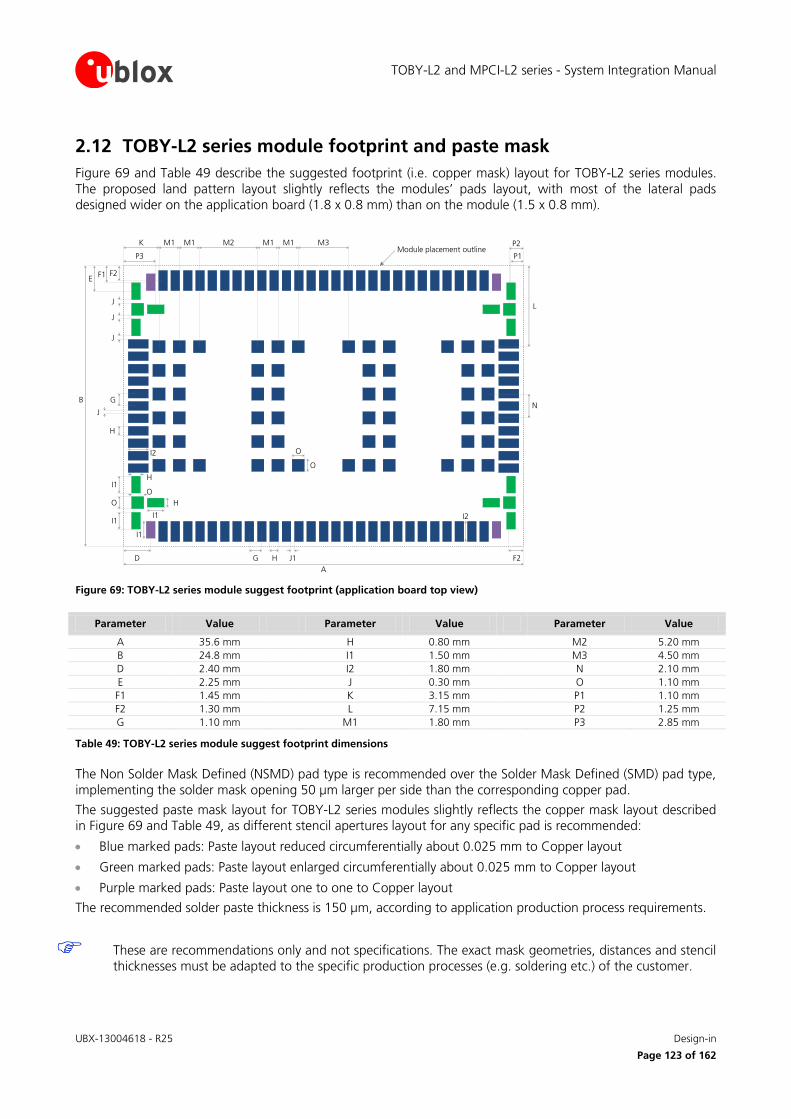
TOBY-L2 and MPCI-L2 series - System Integration Manual
UBX-13004618 - R25 Design-in
Page 123 of 162
2.12 TOBY-L2 series module footprint and paste mask
Figure 69 and Table 49 describe the suggested footprint (i.e. copper mask) layout for TOBY-L2 series modules. The proposed land pattern layout slightly reflects the modules’ pads layout, with most of the lateral pads designed wider on the application board (1.8 x 0.8 mm) than on the module (1.5 x 0.8 mm).
I1
A
G H J1D F2
K M1 M1 M2 P2
B G
H
J
O
O
L
N
M1 M1 M3
I1
I1
O H
J
J
J
E
P3
F1
P1
H
I1
O
I2
I2
F2
Module placement outline
Figure 69: TOBY-L2 series module suggest footprint (application board top view)
Parameter Value Parameter Value Parameter Value
A 35.6 mm H 0.80 mm M2 5.20 mm
B 24.8 mm I1 1.50 mm M3 4.50 mm
D 2.40 mm I2 1.80 mm N 2.10 mm
E 2.25 mm J 0.30 mm O 1.10 mm
F1 1.45 mm K 3.15 mm P1 1.10 mm
F2 1.30 mm L 7.15 mm P2 1.25 mm
G 1.10 mm M1 1.80 mm P3 2.85 mm
Table 49: TOBY-L2 series module suggest footprint dimensions
The Non Solder Mask Defined (NSMD) pad type is recommended over the Solder Mask Defined (SMD) pad type, implementing the solder mask opening 50 µm larger per side than the corresponding copper pad.
The suggested paste mask layout for TOBY-L2 series modules slightly reflects the copper mask layout described in Figure 69 and Table 49, as different stencil apertures layout for any specific pad is recommended:
Blue marked pads: Paste layout reduced circumferentially about 0.025 mm to Copper layout
Green marked pads: Paste layout enlarged circumferentially about 0.025 mm to Copper layout
Purple marked pads: Paste layout one to one to Copper layout
The recommended solder paste thickness is 150 µm, according to application production process requirements.
These are recommendations only and not specifications. The exact mask geometries, distances and stencil thicknesses must be adapted to the specific production processes (e.g. soldering etc.) of the customer.
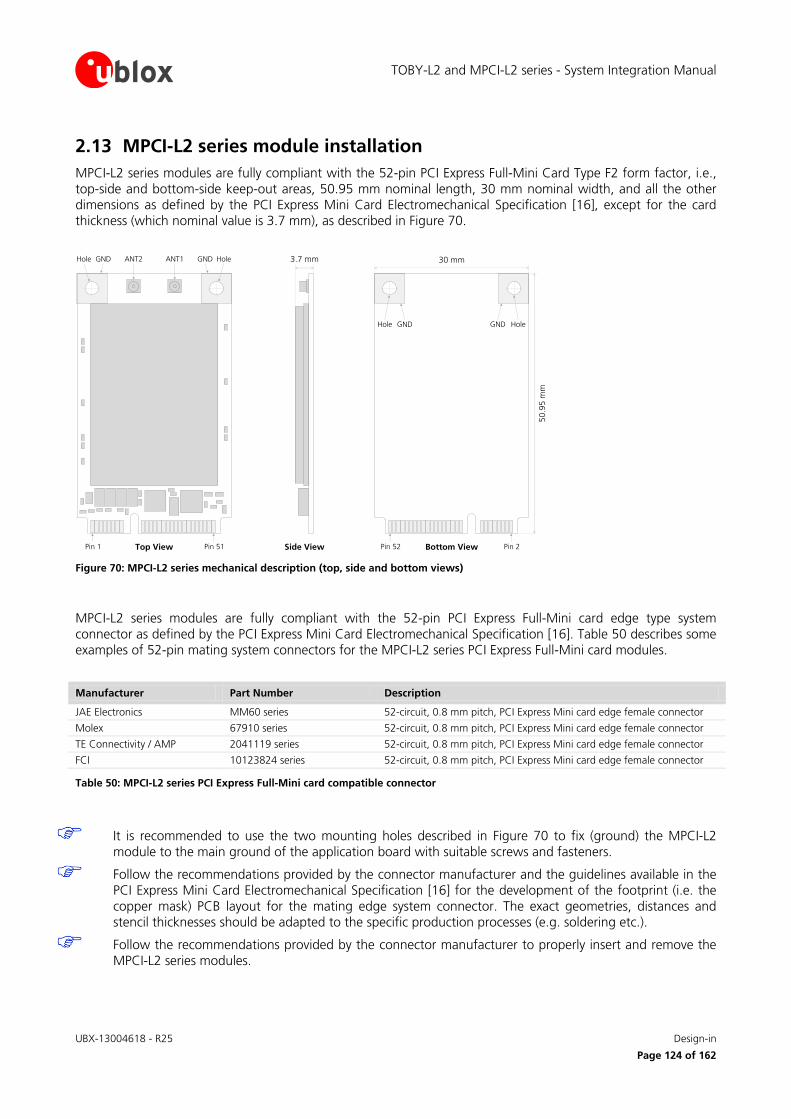
TOBY-L2 and MPCI-L2 series - System Integration Manual
UBX-13004618 - R25 Design-in
Page 124 of 162
2.13 MPCI-L2 series module installation
MPCI-L2 series modules are fully compliant with the 52-pin PCI Express Full-Mini Card Type F2 form factor, i.e., top-side and bottom-side keep-out areas, 50.95 mm nominal length, 30 mm nominal width, and all the other dimensions as defined by the PCI Express Mini Card Electromechanical Specification [16], except for the card thickness (which nominal value is 3.7 mm), as described in Figure 70.
3.7 mm
Side ViewPin 1 Pin 51
ANT1ANT2
Top View
Hole GND HoleGND 30 mm
Pin 52 Pin 2Bottom View
Hole GND HoleGND
50
.95
mm
Figure 70: MPCI-L2 series mechanical description (top, side and bottom views)
MPCI-L2 series modules are fully compliant with the 52-pin PCI Express Full-Mini card edge type system connector as defined by the PCI Express Mini Card Electromechanical Specification [16]. Table 50 describes some examples of 52-pin mating system connectors for the MPCI-L2 series PCI Express Full-Mini card modules.
Manufacturer Part Number Description
JAE Electronics MM60 series 52-circuit, 0.8 mm pitch, PCI Express Mini card edge female connector
Molex 67910 series 52-circuit, 0.8 mm pitch, PCI Express Mini card edge female connector
TE Connectivity / AMP 2041119 series 52-circuit, 0.8 mm pitch, PCI Express Mini card edge female connector
FCI 10123824 series 52-circuit, 0.8 mm pitch, PCI Express Mini card edge female connector
Table 50: MPCI-L2 series PCI Express Full-Mini card compatible connector
It is recommended to use the two mounting holes described in Figure 70 to fix (ground) the MPCI-L2 module to the main ground of the application board with suitable screws and fasteners.
Follow the recommendations provided by the connector manufacturer and the guidelines available in the PCI Express Mini Card Electromechanical Specification [16] for the development of the footprint (i.e. the copper mask) PCB layout for the mating edge system connector. The exact geometries, distances and stencil thicknesses should be adapted to the specific production processes (e.g. soldering etc.).
Follow the recommendations provided by the connector manufacturer to properly insert and remove the MPCI-L2 series modules.
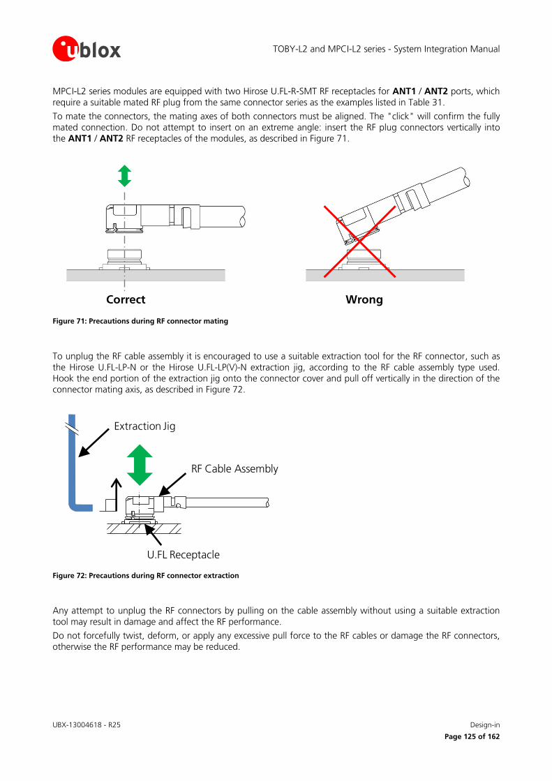
TOBY-L2 and MPCI-L2 series - System Integration Manual
UBX-13004618 - R25 Design-in
Page 125 of 162
MPCI-L2 series modules are equipped with two Hirose U.FL-R-SMT RF receptacles for ANT1 / ANT2 ports, which require a suitable mated RF plug from the same connector series as the examples listed in Table 31.
To mate the connectors, the mating axes of both connectors must be aligned. The "click" will confirm the fully mated connection. Do not attempt to insert on an extreme angle: insert the RF plug connectors vertically into the ANT1 / ANT2 RF receptacles of the modules, as described in Figure 71.
Correct Wrong
Figure 71: Precautions during RF connector mating
To unplug the RF cable assembly it is encouraged to use a suitable extraction tool for the RF connector, such as the Hirose U.FL-LP-N or the Hirose U.FL-LP(V)-N extraction jig, according to the RF cable assembly type used. Hook the end portion of the extraction jig onto the connector cover and pull off vertically in the direction of the connector mating axis, as described in Figure 72.
Extraction Jig
RF Cable Assembly
U.FL Receptacle
Figure 72: Precautions during RF connector extraction
Any attempt to unplug the RF connectors by pulling on the cable assembly without using a suitable extraction tool may result in damage and affect the RF performance.
Do not forcefully twist, deform, or apply any excessive pull force to the RF cables or damage the RF connectors, otherwise the RF performance may be reduced.
TOBY-L2 and MPCI-L2 series - System Integration Manual
UBX-13004618 - R25 Design-in
Page 126 of 162
2.14 Thermal guidelines
Modules’ operating temperature range is specified in TOBY-L2 Data Sheet [1] and MPCI-L2 Data Sheet [2].
The most critical condition concerning module thermal performance is the uplink transmission at maximum power (data upload in connected-mode), when the baseband processor runs at full speed, radio circuits are all active and the RF power amplifier is driven to higher output RF power. This scenario is not often encountered in real networks (for example, see the Terminal Tx Power distribution for WCDMA, taken from operation on a live network, described in the GSMA TS.09 Battery Life Measurement and Current Consumption Technique [17]); however the application should be correctly designed to cope with it.
During transmission at maximum RF power the TOBY-L2 and MPCI-L2 series modules generate thermal power that may exceed 3 W: this is an indicative value since the exact generated power strictly depends on operating condition such as the actual antenna return loss, the number of allocated TX resource blocks, the transmitting frequency band, etc. The generated thermal power must be adequately dissipated through the thermal and mechanical design of the application.
The spreading of the Module-to-Ambient thermal resistance (Rth,M-A) depends on the module operating condition. The overall temperature distribution is influenced by the configuration of the active components during the specific mode of operation and their different thermal resistance toward the case interface.
The Module-to-Ambient thermal resistance value and the relative increase of module temperature will differ according to the specific mechanical deployments of the module, e.g. application PCB with different dimensions and characteristics, mechanical shells enclosure, or forced air flow.
The increase of the thermal dissipation, i.e. the reduction of the Module-to-Ambient thermal resistance, will decrease the temperature of the modules’ internal circuitry for a given operating ambient temperature. This improves the device long-term reliability in particular for applications operating at high ambient temperature.
Recommended hardware techniques to be used to improve heat dissipation in the application:
Connect each GND pin with solid ground layer of the application board and connect each ground area of the multilayer application board with complete thermal via stacked down to main ground layer.
Use the two mounting holes described in Figure 70 to fix (ground) the MPCI-L2 modules to the main ground of the application board with suitable screws and fasteners.
Provide a ground plane as wide as possible on the application board.
Optimize antenna return loss, to optimize overall electrical performance of the module including a decrease of module thermal power.
Optimize the thermal design of any high-power components included in the application, such as linear regulators and amplifiers, to optimize overall temperature distribution in the application device.
Select the material, the thickness and the surface of the box (i.e. the mechanical enclosure) of the application device that integrates the module so that it provides good thermal dissipation.
Follow the thermal guidelines for integrating wireless wide area network mini card add-in cards, such as the MPCI-L2 series modules, as provided in the PCI Express Mini Card Electromechanical Specification [16].
Further hardware techniques that may be considered to improve the heat dissipation in the application:
Force ventilation air-flow within mechanical enclosure.
Provide a heat sink component attached to the module top side, with electrically insulated / high thermal conductivity adhesive, or on the backside of the application board, below the cellular module, as a large part of the heat is transported through the GND pads of the TOBY-L2 series LGA modules and dissipated over the backside of the application board.
TOBY-L2 and MPCI-L2 series - System Integration Manual
UBX-13004618 - R25 Design-in
Page 127 of 162
For example, the Module-to-Ambient thermal resistance (Rth,M-A) is strongly reduced with forced air ventilation and a heat-sink installed on the back of the application board, decreasing the module temperature variation.
Beside the reduction of the Module-to-Ambient thermal resistance implemented by proper application hardware design, the increase of module temperature can be moderated by proper application software implementation:
Enable power saving configuration using the AT+UPSV command (see section 1.15.16).
Enable module connected-mode for a given time period and then disable it for a time period enough long to properly mitigate temperature increase.
2.15 ESD guidelines
The sections 2.15.1 and 2.15.2 are related to EMC / ESD immunity. The modules are ESD sensitive devices. The ESD sensitivity for each pin (as Human Body Model according to JESD22-A114F) is specified in TOBY-L2 series Data Sheet [1] or MPCI-L2 series Data Sheet [2]. Special precautions are required when handling the pins; for ESD handling guidelines see section 3.2.
2.15.1 ESD immunity test overview
The immunity of devices integrating TOBY-L2 and MPCI-L2 series modules to Electro-Static Discharge (ESD) is part of the Electro-Magnetic Compatibility (EMC) conformity which is required for products bearing the CE marking, compliant with the Radio Equipment Directive (2014/53/EU), the EMC Directive (2014/30/EU) and the Low Voltage Directive (2014/35/EU) issued by the Commission of the European Community.
Compliance with these directives implies conformity to the following European Norms for device ESD immunity: ESD testing standard CENELEC EN 61000-4-2 [18] and the radio equipment standards ETSI EN 301 489-1 [19], ETSI EN 301 489-52 [20], which requirements are summarized in Table 51.
The ESD immunity test is performed at the enclosure port, defined by ETSI EN 301 489-1 [19] as the physical boundary through which the electromagnetic field radiates. If the device implements an integral antenna, the enclosure port is seen as all insulating and conductive surfaces housing the device. If the device implements a removable antenna, the antenna port can be separated from the enclosure port. The antenna port includes the antenna element and its interconnecting cable surfaces.
The applicability of ESD immunity test to the whole device depends on the device classification as defined by ETSI EN 301 489-1 [19]. Applicability of ESD immunity test to the relative device ports or the relative interconnecting cables to auxiliary equipment, depends on device accessible interfaces and manufacturer requirements, as defined by ETSI EN 301 489-1 [19].
Contact discharges are performed at conductive surfaces, while air discharges are performed at insulating surfaces. Indirect contact discharges are performed on the measurement setup horizontal and vertical coupling planes as defined in CENELEC EN 61000-4-2 [18].
For the definition of integral antenna, removable antenna, antenna port and device classification see ETSI EN 301 489-1 [19]. For the contact / air discharges definitions see CENELEC EN 61000-4-2 [18].
Application Category Immunity Level
All exposed surfaces of the radio equipment and ancillary equipment in a representative configuration
Contact Discharge 4 kV
Air Discharge 8 kV
Table 51: EMC / ESD immunity requirements as defined by CENELEC EN 61000-4-2 and ETSI EN 301 489-1, ETSI EN 301 489-52
TOBY-L2 and MPCI-L2 series - System Integration Manual
UBX-13004618 - R25 Design-in
Page 128 of 162
2.15.2 ESD immunity test of TOBY-L2 and MPCI-L2 series reference designs
Although EMC / ESD certification is required for customized devices integrating TOBY-L2 and MPCI-L2 series modules for European Conformance CE mark, EMC certification (including ESD immunity) has been successfully performed on TOBY-L2 and MPCI-L2 series modules reference design according to European Norms summarized in Table 51.
The EMC / ESD approved u-blox reference designs consist of a TOBY-L2 and MPCI-L2 series module installed onto a motherboard which provides supply interface, SIM card and communication port. External LTE/3G/2G antennas are connected to the provided connectors.
Since external antennas are used, the antenna port can be separated from the enclosure port. The reference design is not enclosed in a box so that the enclosure port is not identified with physical surfaces. Therefore, some test cases cannot be applied. Only the antenna port is identified as accessible for direct ESD exposure.
Table 52 reports the u-blox TOBY-L2 and MPCI-L2 series reference designs ESD immunity test results, according to test requirements stated in CENELEC EN 61000-4-2 [18], ETSI EN 301 489-1 [19], ETSI EN 301 489-52 [20].
Category Application Immunity Level Remarks
Contact Discharge to coupling planes
(indirect contact discharge)
Enclosure +4 kV / -4 kV
Contact Discharges to conducted surfaces
(direct contact discharge)
Enclosure port Not Applicable Test not applicable to u-blox reference design because it does not provide enclosure surface.
The test is applicable only to equipment providing conductive enclosure surface.
Antenna ports +4 kV / -4 kV Test applicable to u-blox reference design because it
provides antennas with conductive & insulating surfaces.
The test is applicable only to equipment providing antennas with conductive surface.
Air Discharge at insulating surfaces
Enclosure port Not Applicable Test not applicable to the u-blox reference design because it does not provide an enclosure surface.
The test is applicable only to equipment providing insulating enclosure surface.
Antenna ports +8 kV / -8 kV Test applicable to u-blox reference design because it provides antennas with conductive & insulating surfaces.
The test is applicable only to equipment providing
antennas with insulating surface.
Table 52: Enclosure ESD immunity level of u-blox TOBY-L2 and MPCI-L2 series modules reference designs
TOBY-L2 and MPCI-L2 reference design implement all the ESD precautions described in section 2.15.3.
2.15.3 ESD application circuits
The application circuits described in this section are recommended and should be implemented in the device integrating TOBY-L2 and MPCI-L2 series modules, according to the application device classification (see ETSI EN 301 489-1 [19]), to satisfy the requirements for ESD immunity test summarized in Table 51.
Antenna interface
The ANT1 and ANT2 ports of TOBY-L2 and MPCI-L2 series modules provide ESD immunity up to ±4 kV for direct Contact Discharge and up to ±8 kV for Air Discharge: no further precaution to ESD immunity test is needed, as implemented in the EMC / ESD approved reference design of TOBY-L2 and MPCI-L2 series modules.
TOBY-L2 and MPCI-L2 series - System Integration Manual
UBX-13004618 - R25 Design-in
Page 129 of 162
The antenna interface application circuit implemented in the EMC / ESD approved reference designs of TOBY-L2 and MPCI-L2 series modules is described in Figure 48 in case of antennas detection circuit not implemented, and is described in Figure 49 and Table 35 in case of antennas detection circuit implemented (section 2.4).
RESET_N and PERST# pin
The following precautions are suggested for the RESET_N and the PERST# line of TOBY-L2 and MPCI-L2 series modules, depending on the application board handling, to satisfy ESD immunity test requirements:
It is recommended to keep the connection line to RESET_N and PERST# as short as possible
Maximum ESD sensitivity rating of the RESET_N and the PERST# pin is 1 kV (Human Body Model according to JESD22-A114). Higher protection level could be required if the RESET_N or PERST# pin is externally accessible on the application board. The following precautions are suggested to achieve higher protection level:
A general purpose ESD protection device (e.g. EPCOS CA05P4S14THSG varistor array or EPCOS CT0402S14AHSG varistor) should be mounted on the RESET_N or PERST# line, close to accessible point
The RESET_N and PERST# application circuit implemented in the EMC / ESD approved reference designs of TOBY-L2 and MPCI-L2 series modules is described in Figure 43 and Table 30 (section 2.3.2).
SIM interface
The following precautions are suggested for TOBY-L2 and MPCI-L2 series modules SIM interface, depending on the application board handling, to satisfy ESD immunity test requirements:
A bypass capacitor of about 22 pF to 47 pF (e.g. Murata GRM1555C1H470J) must be mounted on the lines connected to the SIM interface pins to assure SIM interface functionality when an electrostatic discharge is applied to the application board enclosure
It is suggested to use as short as possible connection lines at SIM pins
Maximum ESD sensitivity rating of SIM interface pins is 1 kV (Human Body Model according to JESD22-A114). Higher protection level could be required if SIM interface pins are externally accessible on the application board. The following precautions are suggested to achieve higher protection level:
A low capacitance (i.e. less than 10 pF) ESD protection device (e.g. Tyco Electronics PESD0402-140) should be mounted on each SIM interface line, close to accessible points (i.e. close to the SIM card holder)
The SIM interface application circuit implemented in the EMC / ESD approved reference designs of TOBY-L2 and MPCI-L2 series modules is described in Figure 50 and Table 36 (section 2.5).
Other pins and interfaces
All the module pins that are externally accessible on the device integrating TOBY-L2 and MPCI-L2 series module should be included in the ESD immunity test since they are considered to be a port as defined in ETSI EN 301 489-1 [19]. Depending on applicability, to satisfy ESD immunity test requirements according to ESD category level, all the module pins that are externally accessible should be protected up to ±4 kV for direct Contact Discharge and up to ±8 kV for Air Discharge applied to the enclosure surface.
The maximum ESD sensitivity rating of all the other pins of the module is 1 kV (Human Body Model according to JESD22-A114). Higher protection level could be required if the relative pin is externally accessible on the application board. The following precautions are suggested to achieve higher protection level:
USB interface: a very low capacitance (i.e. less or equal to 1 pF) ESD protection device (e.g. Tyco Electronics PESD0402-140 ESD protection device) should be mounted on the USB_D+ and USB_D- lines, close to the accessible points (i.e. close to the USB connector)
Other pins: a general purpose ESD protection device (e.g. EPCOS CA05P4S14THSG varistor array or EPCOS CT0402S14AHSG varistor) should be mounted on the related line, close to accessible point
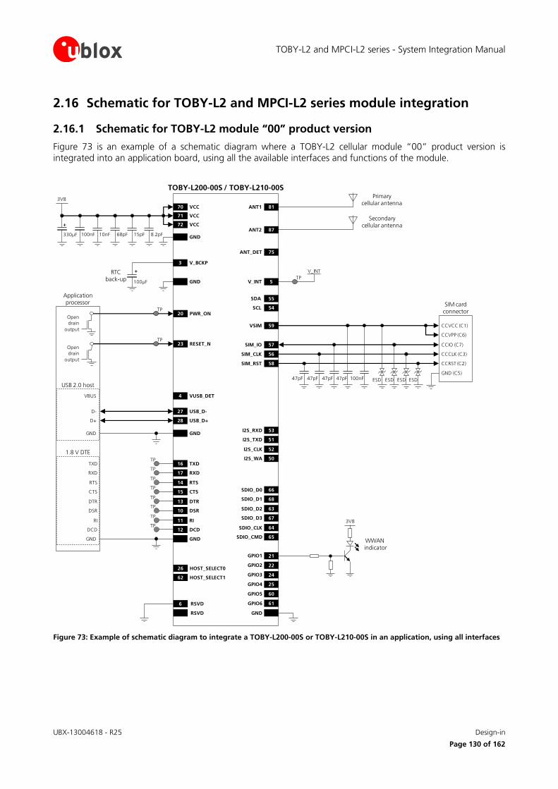
TOBY-L2 and MPCI-L2 series - System Integration Manual
UBX-13004618 - R25 Design-in
Page 130 of 162
2.16 Schematic for TOBY-L2 and MPCI-L2 series module integration
2.16.1 Schematic for TOBY-L2 module “00” product version
Figure 73 is an example of a schematic diagram where a TOBY-L2 cellular module “00” product version is integrated into an application board, using all the available interfaces and functions of the module.
3V8
GND330µF 100nF 10nF
TOBY-L200-00S / TOBY-L210-00S
71 VCC
72 VCC
70 VCC
3 V_BCKP
23 RESET_N
Application processor
Open
drain
output
20 PWR_ON
Open
drain
output
68pF
47pF
SIM card connector
CCVCC (C1)
CCVPP (C6)
CCIO (C7)
CCCLK (C3)
CCRST (C2)
GND (C5)47pF 47pF 100nF
59VSIM
57SIM_IO
56SIM_CLK
58SIM_RST
47pF ESD ESD ESD ESD
81ANT1
87ANT2
Primary cellular antenna
TP
TP
Secondary cellular antenna
5V_INTTP
15pF 8.2pF
+
100µF
+
75ANT_DET
GND
RTC back-up
26 HOST_SELECT0
62 HOST_SELECT1
SDA
SCL
55
54
RSVD
RSVD
6 61GPIO6
22GPIO2
24GPIO3
25GPIO4
60GPIO5
21GPIO1
53I2S_RXD
51I2S_TXD
52I2S_CLK
50I2S_WA
V_INT
16 TXD
17 RXD
12 DCD
14 RTS
15 CTS
13 DTR
10 DSR
11 RI
TP
TP
TP
TP
TP
TP
TP
TPTXD
RXD
DCD
RTS
CTS
DTR
DSR
RI
1.8 V DTE
GND GND
USB 2.0 host
D-
D+
27 USB_D-
28 USB_D+
VBUS 4 VUSB_DET
GND GND 65SDIO_CMD
66SDIO_D0
68SDIO_D1
63SDIO_D2
67SDIO_D3
64SDIO_CLK
GND
3V8
WWANindicator
Figure 73: Example of schematic diagram to integrate a TOBY-L200-00S or TOBY-L210-00S in an application, using all interfaces
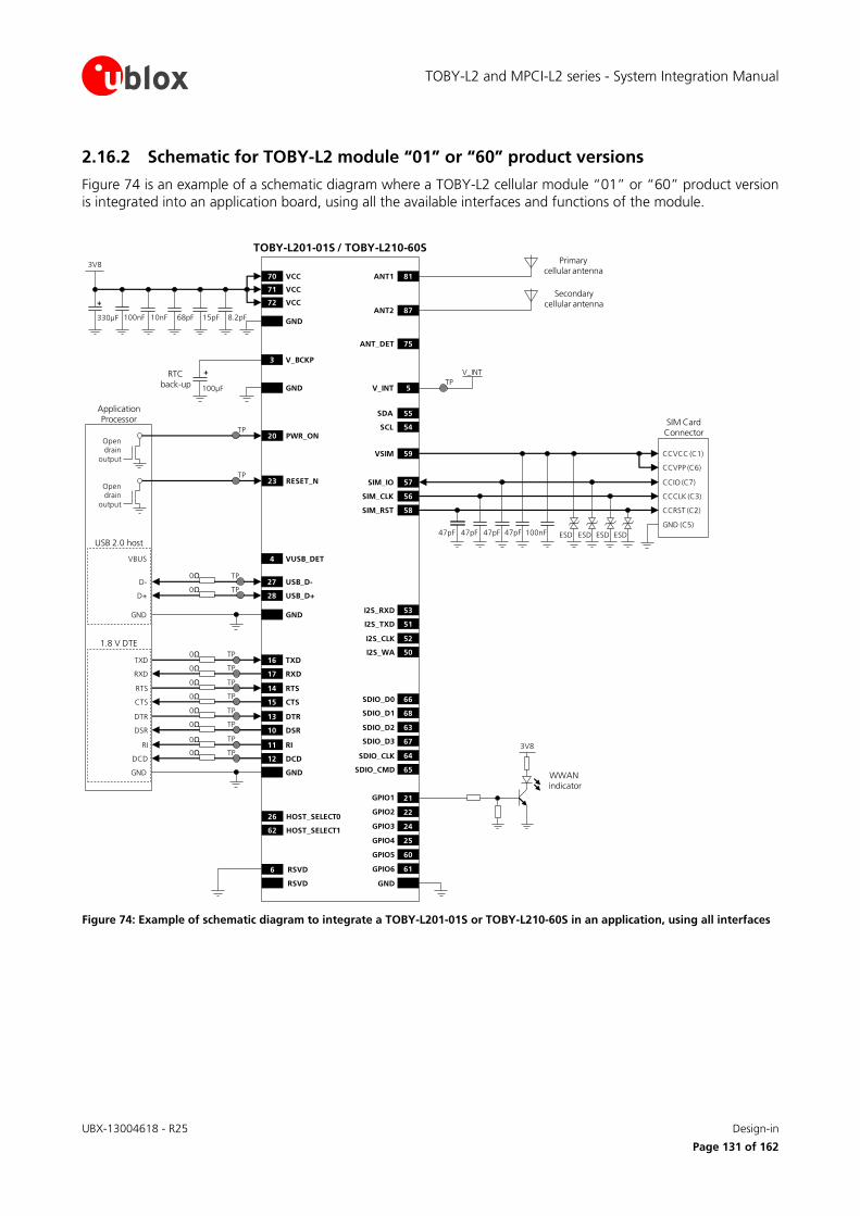
TOBY-L2 and MPCI-L2 series - System Integration Manual
UBX-13004618 - R25 Design-in
Page 131 of 162
2.16.2 Schematic for TOBY-L2 module “01” or “60” product versions
Figure 74 is an example of a schematic diagram where a TOBY-L2 cellular module “01” or “60” product version is integrated into an application board, using all the available interfaces and functions of the module.
3V8
GND330µF 100nF 10nF
TOBY-L201-01S / TOBY-L210-60S
71 VCC
72 VCC
70 VCC
3 V_BCKP
23 RESET_N
Application Processor
Open drain
output
20 PWR_ON
Open drain
output
68pF
47pF
SIM Card Connector
CCVCC (C1)
CCVPP (C6)
CCIO (C7)
CCCLK (C3)
CCRST (C2)
GND (C5)47pF 47pF 100nF
59VSIM
57SIM_IO
56SIM_CLK
58SIM_RST
47pF ESD ESD ESD ESD
81ANT1
87ANT2
Primary cellular antenna
TP
TP
Secondary cellular antenna
5V_INTTP
15pF 8.2pF
+
100µF
+
75ANT_DET
GND
RTC back-up
26 HOST_SELECT0
62 HOST_SELECT1
SDA
SCL
55
54
RSVD
RSVD
6 61GPIO6
22GPIO2
24GPIO3
25GPIO4
60GPIO5
21GPIO1
53I2S_RXD
51I2S_TXD
52I2S_CLK
50I2S_WA
V_INT
16 TXD
17 RXD
12 DCD
14 RTS
15 CTS
13 DTR
10 DSR
11 RI
TP
TP
TP
TP
TP
TP
TP
TPTXD
RXD
DCD
RTS
CTS
DTR
DSR
RI
1.8 V DTE
GND GND
USB 2.0 host
D-
D+
27 USB_D-
28 USB_D+
VBUS 4 VUSB_DET
TP
TP
GND GND 65SDIO_CMD
66SDIO_D0
68SDIO_D1
63SDIO_D2
67SDIO_D3
64SDIO_CLK
GND
0Ω
0Ω
0Ω
0Ω
0Ω
0Ω
0Ω
0Ω
0Ω
0Ω3V8
WWANindicator
Figure 74: Example of schematic diagram to integrate a TOBY-L201-01S or TOBY-L210-60S in an application, using all interfaces
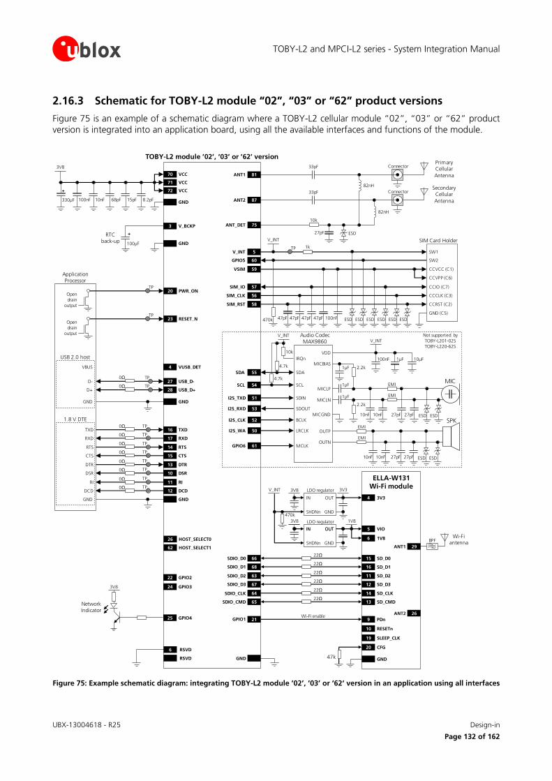
TOBY-L2 and MPCI-L2 series - System Integration Manual
UBX-13004618 - R25 Design-in
Page 132 of 162
2.16.3 Schematic for TOBY-L2 module “02”, “03” or “62” product versions
Figure 75 is an example of a schematic diagram where a TOBY-L2 cellular module “02”, “03” or “62” product version is integrated into an application board, using all the available interfaces and functions of the module.
3V8
GND330µF 100nF 10nF
TOBY-L2 module ’02’, ‘03’ or ’62’ version
71 VCC
72 VCC
70 VCC
3 V_BCKP
68pF 15pF 8.2pF
+
100µF
+
GND
RTC back-up
26 HOST_SELECT0
62 HOST_SELECT1
SDA
SCL
55
54
RSVD
RSVD
6
21GPIO1Wi-Fi enable
ELLA-W131Wi-Fi module
ANT1 29
ANT2 26
BPF
LDO regulator3V8
OUTIN VIO5
1V86
LDO regulator 3V33V8
OUTIN
GNDSHDNn
3V34
1V8
OUTIN
GNDSHDNn
V_INT
470k
65SDIO_CMD
66SDIO_D0
68SDIO_D1
63SDIO_D2
67SDIO_D3
64SDIO_CLK
22Ω
22Ω
22Ω
22Ω
22Ω
22Ω
SD_D015
SD_D116
SD_D211
SD_D312
SD_CLK14
SD_CMD13
GND
PDn9
RESETn10
SLEEP_CLK19
CFG20
GND47k
Wi-Fi antenna
23 RESET_N
Application Processor
Open
drain
output
20 PWR_ON
Open
drain
output
TP
TP
16 TXD
17 RXD
12 DCD
14 RTS
15 CTS
13 DTR
10 DSR
11 RI
TP
TP
TP
TP
TP
TP
TP
TPTXD
RXD
DCD
RTS
CTS
DTR
DSR
RI
1.8 V DTE
GND GND
USB 2.0 host
D-
D+
27 USB_D-
28 USB_D+
VBUS 4 VUSB_DET
TP
TP
GND GND
0Ω
0Ω
0Ω
0Ω
0Ω
0Ω
0Ω
V_INT
BCLK
LRCLK
Audio Codec MAX9860
SDIN
SDOUT
SDA
SCL
52I2S_CLK
50I2S_WA
51I2S_TXD
53I2S_RXD
61GPIO6 MCLK
IRQn
10k
10µF1µF100nF
VDD
SPK
OUTP
OUTN
MIC
MICBIAS1µF 2.2k
1µF
1µFMICLN
MICLP
MICGND
2.2k
ESD ESD
V_INT
10nF10nF
EMI
EMI
27pF27pF
10nF
EMI
EMI
ESD ESD27pF27pF10nF
47pF
SIM Card Holder
CCVCC (C1)
CCVPP (C6)
CCIO (C7)
CCCLK (C3)
CCRST (C2)
GND (C5)47pF 47pF 100nF
59VSIM
57SIM_IO
56SIM_CLK
58SIM_RST
47pF
SW1
SW2
5V_INT
60GPIO5
470k ESD ESD ESD ESD ESD ESD
1kTP
V_INT
25 GPIO4
3V8
Network Indicator
22 GPIO2
24 GPIO3
0Ω
0Ω
0Ω
87ANT2
75ANT_DET10k
Connector
27pF ESD
Secondary Cellular
Antenna
33pF
82nH
82nH
81
ConnectorPrimary Cellular
Antenna
33pF
ANT1
4.7k
4.7k
Not supported by
TOBY-L201-02S
TOBY-L220-62S
Figure 75: Example schematic diagram: integrating TOBY-L2 module ’02’, ’03’ or ‘62‘ version in an application using all interfaces
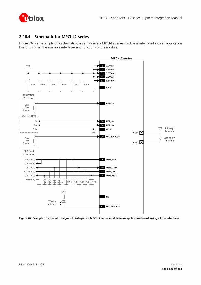
TOBY-L2 and MPCI-L2 series - System Integration Manual
UBX-13004618 - R25 Design-in
Page 133 of 162
2.16.4 Schematic for MPCI-L2 series
Figure 76 is an example of a schematic diagram where a MPCI-L2 series module is integrated into an application board, using all the available interfaces and functions of the module.
3V3
GND
330uF 100nF 10nF
MPCI-L2 series
Application
Processor
Open Drain
Output
22 PERST #
GND GND
USB 2.0 Host
D-
D+
36 USB_D-
38 USB_D+
68pF
Primary
Antenna
Secondary
Antenna
42 LED_WWAN#
15pF 8.2pF
+
20 W_DISABLE #Open Drain
Output
24 3.3Vaux
39 3.3Vaux
2 3.3Vaux
41 3.3Vaux
52 3.3Vaux
3V3
NC
47pF
SIM Card
Connector
CCVCC (C1)
CCVPP (C6)
CCIO (C7)
CCCLK (C3)
CCRST (C2)
GND (C5)47pF47pF100nF
8 UIM_PWR
10 UIM_DATA
12 UIM_CLK
14 UIM_RESET
47pFESDESDESDESD
WWAN
Indicator
ANT1
ANT2
Figure 76: Example of schematic diagram to integrate a MPCI-L2 series module in an application board, using all the interfaces
TOBY-L2 and MPCI-L2 series - System Integration Manual
UBX-13004618 - R25 Design-in
Page 134 of 162
2.17 Design-in checklist
This section provides a design-in checklist.
2.17.1 Schematic checklist
The following are the most important points for a simple schematic check:
DC supply must provide a nominal voltage at VCC / 3.3Vaux pin within the operating range limits.
DC supply must be capable of supporting both the highest peak and the highest averaged current consumption values in connected-mode, as specified in the TOBY-L2 series Data Sheet [1] or in the MPCI-L2 series Data Sheet [2].
VCC / 3.3Vaux voltage supply should be clean, with very low ripple/noise: provide the suggested bypass capacitors, in particular if the application device integrates an internal antenna.
Do not apply loads which might exceed the limit for maximum available current from V_INT supply.
Check that voltage level of any connected pin does not exceed the relative operating range.
Check USB_D+ / USB_D- signal lines as well as very low capacitance ESD protections if accessible.
Capacitance and series resistance must be limited on each SIM signal to match the SIM specifications.
Insert the suggested capacitors on each SIM signal and low capacitance ESD protections if accessible.
Check UART signals direction, as the TOBY-L2 signal names follow the ITU-T V.24 Recommendation [8].
Consider providing appropriate low value series damping resistors on SDIO lines to avoid reflections.
Add a proper pull-up resistor (e.g. 4.7 k) to V_INT or another proper 1.8 V supply on each DDC (I2C)
interface line, if the interface is used.
Check the digital audio interface specifications to connect a proper external audio device.
Consider passive filtering parts on each used analog audio line.
Provide accessible test points directly connected to the following pins of the TOBY-L2 series modules: V_INT, PWR_ON and RESET_N for diagnostic purpose.
Provide accessible test points directly connected to all the UART pins of the TOBY-L2 series modules
(TXD, RXD, RTS, CTS, DTR, DSR, DCD, RI) for diagnostic purpose, in particular providing a 0 series jumper on each line to detach each UART pin of the module from the DTE application processor.
If the USB is not used, provide accessible test points directly connected to the USB_D+ and USB_D- pins
Provide proper precautions for EMC / ESD immunity as required on the application board.
Do not apply voltage to any generic digital interface pin of TOBY-L2 series modules before the switch-on of the generic digital interface supply source (V_INT).
All unused pins can be left unconnected except the RSVD pin number 6 of TOBY-L2 series modules, which must be connected to GND.
TOBY-L2 and MPCI-L2 series - System Integration Manual
UBX-13004618 - R25 Design-in
Page 135 of 162
2.17.2 Layout checklist
The following are the most important points for a simple layout check:
Check 50 nominal characteristic impedance of the RF transmission line connected to the ANT1 and the ANT2 ports (antenna RF interfaces).
Ensure no coupling occurs between the RF interface and noisy or sensitive signals (primarily analog audio input/output signals, SIM signals, high-speed digital lines such as SDIO, USB and other data lines).
Optimize placement for minimum length of RF line.
Check the footprint and paste mask designed for TOBY-L2 module as illustrated in section 2.12.
VCC / 3.3Vaux line should be wide and as short as possible.
Route VCC / 3.3Vaux supply line away from RF lines / parts and other sensitive analog lines / parts.
The VCC / 3.3Vaux bypass capacitors in the picoFarad range should be placed as close as possible to the VCC / 3.3Vaux pins, in particular if the application device integrates an internal antenna.
Ensure an optimal grounding connecting each GND pin with application board solid ground layer.
Use as many vias as possible to connect the ground planes on multilayer application board, providing a dense line of vias at the edges of each ground area, in particular along RF and high speed lines.
Keep routing short and minimize parasitic capacitance on the SIM lines to preserve signal integrity.
USB_D+ / USB_D- traces should meet the characteristic impedance requirement (90 differential and
30 common mode) and should not be routed close to any RF line / part.
Keep the SDIO traces short, avoid stubs, avoid coupling with any RF line / part and consider low value series damping resistors to avoid reflections and other losses in signal integrity.
Ensure appropriate RF precautions for the Wi-Fi and Cellular technologies coexistence as described in section 2.6.4 and in the Wi-Fi / Cellular Integration Application Note [15].
Ensure appropriate RF precautions for the GNSS and Cellular technologies coexistence as described in the GNSS Implementation Application Note [14].
Route analog audio signals away from noisy sources (primarily RF interface, VCC, switching supplies).
The audio outputs lines on the application board must be wide enough to minimize series resistance.
2.17.3 Antenna checklist
Antenna termination should provide 50 characteristic impedance with V.S.W.R at least less than 3:1 (recommended 2:1) on operating bands in deployment geographical area.
Follow the recommendations of the antenna producer for correct antenna installation and deployment (PCB layout and matching circuitry).
Ensure compliance with any regulatory agency RF radiation requirement, as reported in sections 4.2.2 and/or 4.3.1 for products marked with the FCC and/or IC.
Ensure high and similar efficiency for both the primary (ANT1) and the secondary (ANT2) antenna.
Ensure high isolation between the primary (ANT1) and the secondary (ANT2) antenna.
Ensure low Envelope Correlation Coefficient between the primary (ANT1) and the secondary (ANT2) antenna: the 3D antenna radiation patterns should have radiation lobes in different directions.
Ensure high isolation between the cellular antennas and any other antenna or transmitter.
TOBY-L2 and MPCI-L2 series - System Integration Manual
UBX-13004618 - R25 Handling and soldering
Page 136 of 162
3 Handling and soldering
No natural rubbers, no hygroscopic materials or materials containing asbestos are employed.
3.1 Packaging, shipping, storage and moisture preconditioning
For information pertaining to TOBY-L2 series reels / tapes, MPCI-L2 series trays, Moisture Sensitivity levels (MSD), shipment and storage information, as well as drying for preconditioning, see the TOBY-L2 series Data Sheet [1], the MPCI-L2 series Data Sheet [2] and the u-blox Package Information Guide [27].
3.2 Handling
The TOBY-L2 and MPCI-L2 series modules are Electro-Static Discharge (ESD) sensitive devices.
Ensure ESD precautions are implemented during handling of the module.
Electrostatic discharge (ESD) is the sudden and momentary electric current that flows between two objects at different electrical potentials caused by direct contact or induced by an electrostatic field. The term is usually used in the electronics and other industries to describe momentary unwanted currents that may cause damage to electronic equipment.
The ESD sensitivity for each pin of TOBY-L2 and MPCI-L2 series modules (as Human Body Model according to JESD22-A114F) is specified in the TOBY-L2 series Data Sheet [1] or the MPCI-L2 series Data Sheet [2].
ESD prevention is based on establishing an Electrostatic Protective Area (EPA). The EPA can be a small working station or a large manufacturing area. The main principle of an EPA is that there are no highly charging materials near ESD sensitive electronics, all conductive materials are grounded, workers are grounded, and charge build-up on ESD sensitive electronics is prevented. International standards are used to define typical EPA and can be obtained for example from International Electrotechnical Commission (IEC) or American National Standards Institute (ANSI).
In addition to standard ESD safety practices, the following measures should be taken into account whenever handling the TOBY-L2 and MPCI-L2 series modules:
Unless there is a galvanic coupling between the local GND (i.e. the work table) and the PCB GND, then the first point of contact when handling the PCB must always be between the local GND and PCB GND.
Before mounting an antenna patch, connect ground of the device.
When handling the module, do not come into contact with any charged capacitors and be careful when contacting materials that can develop charges (e.g. patch antenna, coax cable, soldering iron,…).
To prevent electrostatic discharge through the RF pin, do not touch any exposed antenna area. If there is any risk that such exposed antenna area is touched in non ESD protected work area, implement proper ESD protection measures in the design.
When soldering the module and patch antennas to the RF pin, make sure to use an ESD safe soldering iron.
For more robust designs, employ additional ESD protection measures on the application device integrating the TOBY-L2 and MPCI-L2 series modules, as described in section 2.15.3.
TOBY-L2 and MPCI-L2 series - System Integration Manual
UBX-13004618 - R25 Handling and soldering
Page 137 of 162
3.3 Soldering
3.3.1 Soldering paste
"No Clean" soldering paste is strongly recommended for TOBY-L2 series modules, as it does not require cleaning after the soldering process has taken place. The paste listed in the example below meets these criteria.
Soldering Paste: OM338 SAC405 / Nr.143714 (Cookson Electronics)
Alloy specification: 95.5% Sn / 3.9% Ag / 0.6% Cu (95.5% Tin / 3.9% Silver / 0.6% Copper)
95.5% Sn / 4.0% Ag / 0.5% Cu (95.5% Tin / 4.0% Silver / 0.5% Copper)
Melting Temperature: 217 °C
Stencil Thickness: 150 µm for base boards
The final choice of the soldering paste depends on the approved manufacturing procedures.
The paste-mask geometry for applying soldering paste should meet the recommendations in section 2.12.
The quality of the solder joints on the connectors (“half vias”) should meet the appropriate IPC specification.
3.3.2 Reflow soldering
A convection type-soldering oven is strongly recommended for TOBY-L2 series modules over the infrared type radiation oven. Convection heated ovens allow precise control of the temperature and all parts will be heated up evenly, regardless of material properties, thickness of components and surface color.
Consider the ”IPC-7530 Guidelines for temperature profiling for mass soldering (reflow and wave) processes”, published 2001.
Reflow profiles are to be selected according to the following recommendations.
Failure to observe these recommendations can result in severe damage to the device!
Preheat phase
Initial heating of component leads and balls. Residual humidity will be dried out. Note that this preheat phase will not replace prior baking procedures.
Temperature rise rate: max 3 °C/s If the temperature rise is too rapid in the preheat phase it may cause excessive slumping.
Time: 60 – 120 s If the preheat is insufficient, rather large solder balls tend to be generated. Conversely, if performed excessively, fine balls and large balls will be generated in clusters.
End Temperature: 150 - 200 °C If the temperature is too low, non-melting tends to be caused in areas containing large heat capacity.
Heating/ reflow phase
The temperature rises above the liquidus temperature of 217 °C. Avoid a sudden rise in temperature as the slump of the paste could become worse.
Limit time above 217 °C liquidus temperature: 40 - 60 s
Peak reflow temperature: 245 °C
Cooling phase
A controlled cooling avoids negative metallurgical effects (solder becomes more brittle) of the solder and possible mechanical tensions in the products. Controlled cooling helps to achieve bright solder fillets with a good shape and low contact angle.
Temperature fall rate: max 4 °C/s
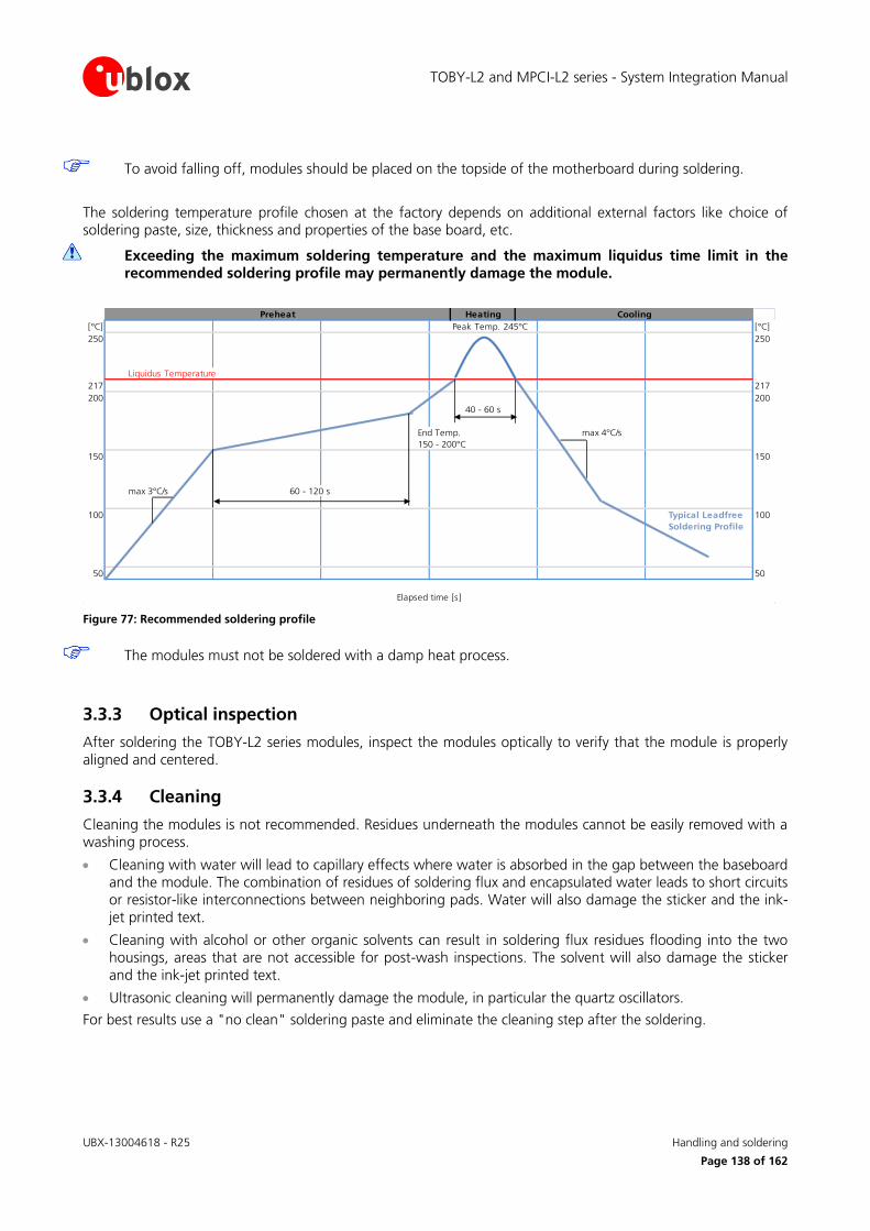
TOBY-L2 and MPCI-L2 series - System Integration Manual
UBX-13004618 - R25 Handling and soldering
Page 138 of 162
To avoid falling off, modules should be placed on the topside of the motherboard during soldering.
The soldering temperature profile chosen at the factory depends on additional external factors like choice of soldering paste, size, thickness and properties of the base board, etc.
Exceeding the maximum soldering temperature and the maximum liquidus time limit in the recommended soldering profile may permanently damage the module.
Preheat Heating Cooling
[°C] Peak Temp. 245°C [°C]
250 250
Liquidus Temperature
217 217
200 200
40 - 60 s
End Temp. max 4°C/s
150 - 200°C
150 150
max 3°C/s 60 - 120 s
100 Typical Leadfree 100
Soldering Profile
50 50
Elapsed time [s]
Figure 77: Recommended soldering profile
The modules must not be soldered with a damp heat process.
3.3.3 Optical inspection
After soldering the TOBY-L2 series modules, inspect the modules optically to verify that the module is properly aligned and centered.
3.3.4 Cleaning
Cleaning the modules is not recommended. Residues underneath the modules cannot be easily removed with a washing process.
Cleaning with water will lead to capillary effects where water is absorbed in the gap between the baseboard and the module. The combination of residues of soldering flux and encapsulated water leads to short circuits or resistor-like interconnections between neighboring pads. Water will also damage the sticker and the ink-jet printed text.
Cleaning with alcohol or other organic solvents can result in soldering flux residues flooding into the two housings, areas that are not accessible for post-wash inspections. The solvent will also damage the sticker and the ink-jet printed text.
Ultrasonic cleaning will permanently damage the module, in particular the quartz oscillators.
For best results use a "no clean" soldering paste and eliminate the cleaning step after the soldering.
TOBY-L2 and MPCI-L2 series - System Integration Manual
UBX-13004618 - R25 Handling and soldering
Page 139 of 162
3.3.5 Repeated reflow soldering
Only a single reflow soldering process is encouraged for boards with a module populated on it.
3.3.6 Wave soldering
Boards with combined through-hole technology (THT) components and surface-mount technology (SMT) devices require wave soldering to solder the THT components. TOBY-L2 series LGA modules must not be soldered with a wave soldering process.
3.3.7 Hand soldering
Hand soldering is not recommended.
3.3.8 Rework
Rework is not recommended.
Never attempt a rework on the module itself, e.g. replacing individual components. Such actions immediately terminate the warranty.
3.3.9 Conformal coating
Certain applications employ a conformal coating of the PCB using HumiSeal® or other related coating products.
These materials affect the HF properties of the cellular modules and it is important to prevent them from flowing into the module.
The RF shields do not provide 100% protection for the module from coating liquids with low viscosity, therefore care is required in applying the coating.
Conformal Coating of the module will void the warranty.
3.3.10 Casting
If casting is required, use viscose or another type of silicon pottant. The OEM is strongly advised to qualify such processes in combination with the cellular modules before implementing this in the production.
Casting will void the warranty.
3.3.11 Grounding metal covers
Attempts to improve grounding by soldering ground cables, wick or other forms of metal strips directly onto the EMI covers is done at the customer's own risk. The numerous ground pins should be sufficient to provide optimum immunity to interferences and noise.
u-blox gives no warranty for damages to the cellular modules caused by soldering metal cables or any other forms of metal strips directly onto the EMI covers.
3.3.12 Use of ultrasonic processes
The cellular modules contain components which are sensitive to Ultrasonic Waves. Use of any Ultrasonic Processes (cleaning, welding etc.) may cause damage to the module.
u-blox gives no warranty against damages to the cellular modules caused by any Ultrasonic Processes.
TOBY-L2 and MPCI-L2 series - System Integration Manual
UBX-13004618 - R25 Approvals
Page 140 of 162
4 Approvals
For the complete list and details regarding all the certification schemes approvals of TOBY-L2 and MPCI-L2 series modules, see the TOBY-L2 Data Sheet [1] and the MPCI-L2 Data Sheet [2], or visit our website (www.u-blox.com), or please contact the u-blox office or sales representative nearest you.
4.1 Product certification approval overview
Product certification approval is the process of certifying that a product has passed all tests and criteria required by specifications, typically called “certification schemes” that can be divided into three distinct categories:
Regulatory certification
o Country specific approval required by local government in most regions and countries, such as:
CE (Conformité Européenne) marking for European Union
FCC (Federal Communications Commission) approval for United States
Industry certification
o Telecom industry specific approval verifying the interoperability between devices and networks:
GCF (Global Certification Forum), partnership between European device manufacturers and network operators to ensure and verify global interoperability between devices and networks
PTCRB (PCS Type Certification Review Board), created by United States network operators to ensure and verify interoperability between devices and North America networks
Operator certification
o Operator specific approval required by some mobile network operator, such as:
AT&T network operator in United States
Even if TOBY-L2 and MPCI-L2 series modules are approved under all major certification schemes, the application device that integrates TOBY-L2 and MPCI-L2 series modules must be approved under all the certification schemes required by the specific application device to be deployed in the market.
The required certification scheme approvals and relative testing specifications differ depending on the country or the region where the device that integrates TOBY-L2 and MPCI-L2 series modules must be deployed, on the relative vertical market of the device, on type, features and functionalities of the whole application device, and on the network operators where the device must operate.
Check the appropriate applicability of the TOBY-L2 / MPCI-L2 module’s approvals while starting the certification process of the device integrating the module: the re-use of the u-blox cellular module’s approval can significantly reduce the cost and time to market of the application device certification.
The certification of the application device that integrates a TOBY-L2 module or a MPCI-L2 module and the compliance of the application device with all the applicable certification schemes, directives and standards are the sole responsibility of the application device manufacturer.
TOBY-L2 and MPCI-L2 series modules are certified according to all capabilities and options stated in the Protocol Implementation Conformance Statement document (PICS) of the module. The PICS, according to the 3GPP TS 51.010-2 [21], 3GPP TS 34.121-2 [22], 3GPP TS 36.521-2 [24] and 3GPP TS 36.523-2 [25], is a statement of the implemented and supported capabilities and options of a device.
The PICS document of the application device integrating TOBY-L2 and MPCI-L2 series modules must be updated from the module PICS statement if any feature stated as supported by the module in its PICS document is not implemented or disabled in the application device. For more details regarding the AT commands settings that affect the PICS, see the u-blox AT Commands Manual [3].
Check the specific settings required for mobile network operators approvals as they may differ from the AT commands settings defined in the module as integrated in the application device.
TOBY-L2 and MPCI-L2 series - System Integration Manual
UBX-13004618 - R25 Approvals
Page 141 of 162
4.2 US Federal Communications Commission notice
United States Federal Communications Commission (FCC) IDs:
u-blox TOBY-L200 cellular modules: XPYTOBYL200
u-blox TOBY-L201 cellular modules: XPYTOBYL201
u-blox TOBY-L210 cellular modules: XPYTOBYL210
u-blox TOBY-L280 cellular modules: XPYTOBYL280
u-blox MPCI-L200 cellular modules: Contains FCC ID XPYTOBYL200
u-blox MPCI-L201 cellular modules: Contains FCC ID XPYTOBYL201
u-blox MPCI-L210 cellular modules: Contains FCC ID XPYTOBYL210
u-blox MPCI-L280 cellular modules: Contains FCC ID XPYTOBYL280
4.2.1 Safety warnings review the structure
Equipment for building-in. The requirements for fire enclosure must be evaluated in the end product
The clearance and creepage current distances required by the end product must be withheld when the module is installed
The cooling of the end product shall not negatively be influenced by the installation of the module
Excessive sound pressure from earphones and headphones can cause hearing loss
No natural rubbers, hygroscopic materials, or materials containing asbestos are employed
4.2.2 Declaration of Conformity
This device complies with Part 15 of the FCC rules. Operation is subject to the following two conditions:
this device may not cause harmful interference
this device must accept any interference received, including interference that may cause undesired operation
Radiofrequency radiation exposure Information: this equipment complies with radiation exposure limits prescribed for an uncontrolled environment for fixed and mobile use conditions. This equipment should be installed and operated with a minimum distance of 20 cm between the radiator and the body of the user or nearby persons. This transmitter must not be co-located or operating in conjunction with any other antenna or transmitter except as authorized in the certification of the product.
The gain of the system antenna(s) used for the TOBY-L200, TOBY-L210, MPCI-L200, MPCI-L210 modules (i.e. the combined transmission line, connector, cable losses and radiating element gain) must not exceed 9.8 dBi (in 700 MHz, i.e. LTE FDD-17 band), 4.3 dBi (in 850 MHz, i.e. GSM 850 or UMTS FDD-5 or LTE FDD-5 band), 5.5 dBi (in 1700 MHz, i.e. AWS or UMTS FDD-4 or LTE FDD-4 band), 2.8 dBi (in 1900 MHz, i.e. GSM 1900 or UMTS FDD-2 or LTE FDD-2 band), 6.0 dBi (in 2500 MHz, i.e. LTE FDD-7 band) for mobile and fixed or mobile operating configurations.
The gain of the system antenna(s) used for TOBY-L201, MPCI-L201 modules (i.e. the combined transmission line, connector, cable losses and radiating element gain) must not exceed 9.8 dBi (700 MHz, i.e. LTE FDD-17 band), 10.2 dBi (750 MHz, i.e. LTE FDD-13 band), 10.0 dBi (850 MHz, i.e. UMTS FDD-5 or LTE FDD-5 band), 6.8 dBi (1700 MHz, i.e. AWS or LTE FDD-4 band), 8.5 dBi (1900 MHz, i.e. UMTS FDD-2 or LTE FDD-2 band) for mobile and fixed or mobile operating configurations.
The gain of the system antenna(s) used for TOBY-L280, MPCI-L280 modules (i.e. the combined transmission line, connector, cable losses and radiating element gain) must not exceed 4.3 dBi (850 MHz, i.e. GSM 850 or UMTS FDD-5 or LTE FDD-5 band), 3.4 dBi (1900 MHz, i.e. GSM 1900 or UMTS FDD-2 or LTE FDD-2 band), 10.8 dBi (2500 MHz, i.e. LTE FDD-7 band) for mobile and fixed or mobile operating configurations.
TOBY-L2 and MPCI-L2 series - System Integration Manual
UBX-13004618 - R25 Approvals
Page 142 of 162
4.2.3 Modifications
The FCC requires the user to be notified that any changes or modifications made to this device that are not expressly approved by u-blox could void the user's authority to operate the equipment.
Manufacturers of mobile or fixed devices incorporating the TOBY-L2 and MPCI-L2 series modules are authorized to use the FCC Grants of the TOBY-L2 series modules for their own final products according to the conditions referenced in the certificates.
The FCC Label shall in the above case be visible from the outside, or the host device shall bear a second label stating:
"Contains FCC ID: XPYTOBYL200" resp.
"Contains FCC ID: XPYTOBYL201" resp.
"Contains FCC ID: XPYTOBYL210" resp.
"Contains FCC ID: XPYTOBYL280" resp.
IMPORTANT: Manufacturers of portable applications incorporating the TOBY-L2 and MPCI-L2 series modules are required to have their final product certified and apply for their own FCC Grant related to the specific portable device. This is mandatory to meet the SAR requirements for portable devices.
Changes or modifications not expressly approved by the party responsible for compliance could void the user's authority to operate the equipment.
Additional Note: as per 47CFR15.105 this equipment has been tested and found to comply with the limits for a Class B digital device, pursuant to part 15 of the FCC Rules. These limits are designed to provide reasonable protection against harmful interference in a residential installation. This equipment generates, uses and can radiate radio frequency energy and, if not installed and used in accordance with the instructions, may cause harmful interference to radio communications. However, there is no guarantee that interference will not occur in a particular installation. If this equipment does cause harmful interference to radio or television reception, which can be determined by turning the equipment off and on, the user is encouraged to try to correct the interference by one or more of the following measures:
o Reorient or relocate the receiving antenna
o Increase the separation between the equipment and receiver
o Connect the equipment into an outlet on a circuit different from that to which the receiver is connected
o Consultant the dealer or an experienced radio/TV technician for help
4.3 Innovation, Science and Economic Development Canada notice
ISED Canada (formerly known as IC - Industry Canada) Certification Numbers:
u-blox TOBY-L200 cellular modules: 8595A-TOBYL200
u-blox TOBY-L201 cellular modules: 8595A-TOBYL201
u-blox TOBY-L210 cellular modules: 8595A-TOBYL210
u-blox TOBY-L280 cellular modules: 8595A-TOBYL280
u-blox MPCI-L200 cellular modules: Contains IC 8595A-TOBYL200
u-blox MPCI-L201 cellular modules: Contains IC 8595A-TOBYL201
u-blox MPCI-L210 cellular modules: Contains IC 8595A-TOBYL210
u-blox MPCI-L280 cellular modules: Contains IC 8595A-TOBYL280
TOBY-L2 and MPCI-L2 series - System Integration Manual
UBX-13004618 - R25 Approvals
Page 143 of 162
4.3.1 Declaration of Conformity
Radiofrequency radiation exposure Information: this equipment complies with radiation exposure limits prescribed for an uncontrolled environment for fixed and mobile use conditions. This equipment should be installed and operated with a minimum distance of 20 cm between the radiator and the body of the user or nearby persons. This transmitter must not be co-located or operating in conjunction with any other antenna or transmitter except as authorized in the certification of the product.
The gain of the system antenna(s) used for the TOBY-L200, TOBY-L210, MPCI-L200, MPCI-L210 modules (i.e. the combined transmission line, connector, cable losses and radiating element gain) must not exceed 9.8 dBi (700 MHz, i.e. LTE FDD-17 band), 4.3 dBi (850 MHz, i.e. GSM 850 or UMTS FDD-5 or LTE FDD-5 band), 5.5 dBi (1700 MHz, i.e. AWS or UMTS FDD-4 or LTE FDD-4 band), 2.8 dBi (1900 MHz, i.e. GSM 1900 or UMTS FDD-2 or LTE FDD-2 band), 6.0 dBi (2500 MHz, i.e. LTE FDD-7 band) for mobile and fixed or mobile operating configurations.
The gain of the system antenna(s) used for TOBY-L201, MPCI-L201 modules (i.e. the combined transmission line, connector, cable losses and radiating element gain) must not exceed 6.7 dBi (700 MHz, i.e. LTE FDD-17 band), 6.9 dBi (750 MHz, i.e. LTE FDD-13 band), 6.7 dBi (850 MHz, i.e. UMTS FDD-5 or LTE FDD-5 band), 6.8 dBi (1700 MHz, i.e. AWS or LTE FDD-4 band), 8.5 dBi (1900 MHz, i.e. UMTS FDD-2 or LTE FDD-2 band) for mobile and fixed or mobile operating configurations.
The gain of the system antenna(s) used for TOBY-L280, MPCI-L280 modules (i.e. the combined transmission line, connector, cable losses and radiating element gain) must not exceed 1.0 dBi (850 MHz, i.e. GSM 850 or UMTS FDD-5 or LTE FDD-5 band), 3.4 dBi (1900 MHz, i.e. GSM 1900 or UMTS FDD-2 or LTE FDD-2 band), 3.3 dBi (2500 MHz, i.e. LTE FDD-7 band) for mobile and fixed or mobile operating configurations.
4.3.2 Modifications
The ISED Canada requires the user to be notified that any changes or modifications made to this device that are not expressly approved by u-blox could void the user's authority to operate the equipment.
Manufacturers of mobile or fixed devices incorporating the TOBY-L2 and MPCI-L2 series modules are authorized to use the ISED Canada Certificates of the TOBY-L2 series modules for their own final products according to the conditions referenced in the certificates.
The ISED Canada Label shall in the above case be visible from the outside, or the host device shall bear a second label stating:
"Contains IC: 8595A-TOBYL200" resp.
"Contains IC: 8595A-TOBYL201" resp.
"Contains IC: 8595A-TOBYL210" resp.
"Contains IC: 8595A-TOBYL280" resp.
Innovation, Science and Economic Development Canada (ISED) Notices
This Class B digital apparatus complies with Canadian CAN ICES-3(B) / NMB-3(B) and RSS-210.
Operation is subject to the following two conditions:
o this device may not cause interference
o this device must accept any interference, including interference that may cause undesired operation of the device
TOBY-L2 and MPCI-L2 series - System Integration Manual
UBX-13004618 - R25 Approvals
Page 144 of 162
Radio Frequency (RF) Exposure Information
The radiated output power of the u-blox Cellular Module is below the Innovation, Science and Economic Development Canada (ISED) radio frequency exposure limits. The u-blox Cellular Module should be used in such a manner such that the potential for human contact during normal operation is minimized.
This device has been evaluated and shown compliant with the ISED RF Exposure limits under mobile exposure conditions (antennas are greater than 20 cm from a person's body).
This device has been certified for use in Canada. Status of the listing in the Innovation, Science and Economic Development’s REL (Radio Equipment List) can be found at the following web address:
http://www.ic.gc.ca/app/sitt/reltel/srch/nwRdSrch.do?lang=eng
Additional Canadian information on RF exposure also can be found at the following web address: http://www.ic.gc.ca/eic/site/smt-gst.nsf/eng/sf08792.html
IMPORTANT: Manufacturers of portable applications incorporating the TOBY-L2 and MPCI-L2 series modules are required to have their final product certified and apply for their own Innovation, Science and Economic Development Certificate related to the specific portable device. This is mandatory to meet the SAR requirements for portable devices.
Changes or modifications not expressly approved by the party responsible for compliance could void the user's authority to operate the equipment.
Canada, avis d'Innovation, Sciences et Développement économique Canada (ISDE)
Cet appareil numérique de classe B est conforme aux normes canadiennes CAN ICES-3B) / NMB-3(B) et CNR-210.
Son fonctionnement est soumis aux deux conditions suivantes:
o cet appareil ne doit pas causer d'interférence
o cet appareil doit accepter toute interférence, notamment les interférences qui peuvent affecter son fonctionnement
Informations concernant l'exposition aux fréquences radio (RF)
La puissance de sortie émise par l’appareil de sans fil u-blox Cellular Module est inférieure à la limite d'exposition aux fréquences radio d'Innovation, Sciences et Développement économique Canada (ISDE). Utilisez l’appareil de sans fil u-blox Cellular Module de façon à minimiser les contacts humains lors du fonctionnement normal.
Ce périphérique a été évalué et démontré conforme aux limites d'exposition aux fréquences radio (RF) d'ISDE lorsqu'il est installé dans des produits hôtes particuliers qui fonctionnent dans des conditions d'exposition à des appareils mobiles (les antennes se situent à plus de 20 centimètres du corps d'une personne).
Ce périphérique est homologué pour l'utilisation au Canada. Pour consulter l'entrée correspondant à l’appareil dans la liste d'équipement radio (REL - Radio Equipment List) d'Industrie Canada rendez-vous sur:
http://www.ic.gc.ca/app/sitt/reltel/srch/nwRdSrch.do?lang=fra
Pour des informations supplémentaires concernant l'exposition aux RF au Canada rendez-vous sur: http://www.ic.gc.ca/eic/site/smt-gst.nsf/fra/sf08792.html
IMPORTANT: les fabricants d'applications portables contenant les modules TOBY-L2 and MPCI-L2 series doivent faire certifier leur produit final et déposer directement leur candidature pour une certification FCC ainsi que pour un certificat ISDE Canada délivré par l'organisme chargé de ce type d'appareil portable. Ceci est obligatoire afin d'être en accord avec les exigences SAR pour les appareils portables.
Tout changement ou modification non expressément approuvé par la partie responsable de la certification peut annuler le droit d'utiliser l'équipement.
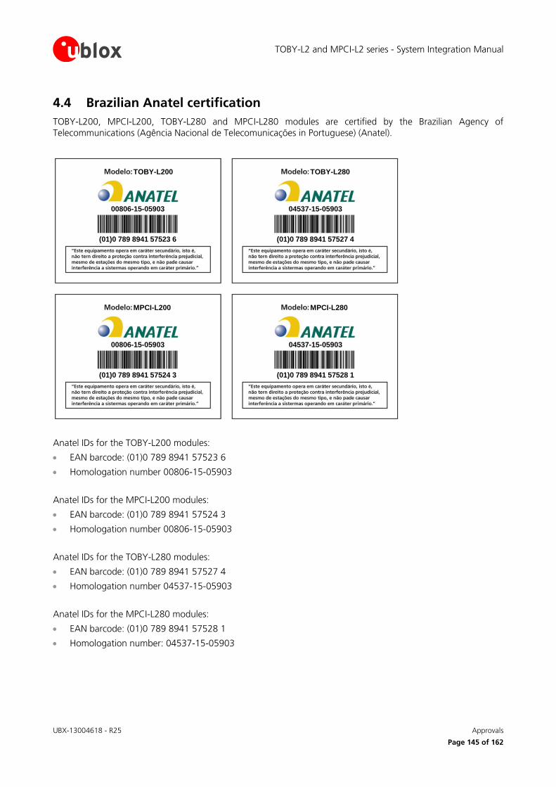
TOBY-L2 and MPCI-L2 series - System Integration Manual
UBX-13004618 - R25 Approvals
Page 145 of 162
4.4 Brazilian Anatel certification
TOBY-L200, MPCI-L200, TOBY-L280 and MPCI-L280 modules are certified by the Brazilian Agency of Telecommunications (Agência Nacional de Telecomunicações in Portuguese) (Anatel).
TOBY-L200
(01)0 789 8941 57523 6
00806-15-05903
TOBY-L280
(01)0 789 8941 57527 4
04537-15-05903
MPCI-L200
(01)0 789 8941 57524 3
00806-15-05903
MPCI-L280
(01)0 789 8941 57528 1
04537-15-05903
Anatel IDs for the TOBY-L200 modules:
EAN barcode: (01)0 789 8941 57523 6
Homologation number 00806-15-05903
Anatel IDs for the MPCI-L200 modules:
EAN barcode: (01)0 789 8941 57524 3
Homologation number 00806-15-05903
Anatel IDs for the TOBY-L280 modules:
EAN barcode: (01)0 789 8941 57527 4
Homologation number 04537-15-05903
Anatel IDs for the MPCI-L280 modules:
EAN barcode: (01)0 789 8941 57528 1
Homologation number: 04537-15-05903
TOBY-L2 and MPCI-L2 series - System Integration Manual
UBX-13004618 - R25 Approvals
Page 146 of 162
4.5 European Conformance CE mark
The TOBY-L2 and MPCI-L2 series cellular modules (except TOBY-L201, MPCI-L201, TOBY-L220 and MPCI-L220) have been evaluated against the essential requirements of the 2014/53/EU Radio Equipment Directive.
In order to satisfy the essential requirements of the 2014/53/EU Radio Equipment Directive, the modules are compliant with the following standards:
Radio Frequency spectrum use (Article 3.2): o EN 301 511 o EN 301 908-1 o EN 301 908-2 o EN 301 908-13
Electromagnetic Compatibility (Article 3.1b): o EN 301 489-1 o EN 301 489-52
Health and Safety (Article 3.1a) o EN 60950-1 o EN 62311
Radiofrequency radiation exposure Information: this equipment complies with radiation exposure limits prescribed for an uncontrolled environment for fixed and mobile use conditions. This equipment should be installed and operated with a minimum distance of 20 cm between the radiator and the body of the user or nearby persons. This transmitter must not be co-located or operating in conjunction with any other antenna or transmitter except as authorized in the certification of the product.
The conformity assessment procedure for the modules, referred to in Article 17 and detailed in Annex II of Directive 2014/53/EU has been followed.
Thus, the following marking is included in the product:
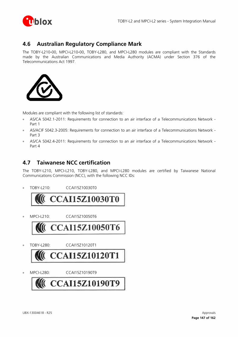
TOBY-L2 and MPCI-L2 series - System Integration Manual
UBX-13004618 - R25 Approvals
Page 147 of 162
4.6 Australian Regulatory Compliance Mark
The TOBY-L210-00, MPCI-L210-00, TOBY-L280, and MPCI-L280 modules are compliant with the Standards made by the Australian Communications and Media Authority (ACMA) under Section 376 of the Telecommunications Act 1997.
Modules are compliant with the following list of standards:
AS/CA S042.1-2011: Requirements for connection to an air interface of a Telecommunications Network - Part 1
AS/ACIF S042.3-2005: Requirements for connection to an air interface of a Telecommunications Network - Part 3
AS/CA S042.4-2011: Requirements for connection to an air interface of a Telecommunications Network - Part 4
4.7 Taiwanese NCC certification
The TOBY-L210, MPCI-L210, TOBY-L280, and MPCI-L280 modules are certified by Taiwanese National Communications Commission (NCC), with the following NCC IDs:
TOBY-L210: CCAI15Z10030T0
MPCI-L210: CCAI15Z10050T6
TOBY-L280: CCAI15Z10120T1
MPCI-L280: CCAI15Z10190T9
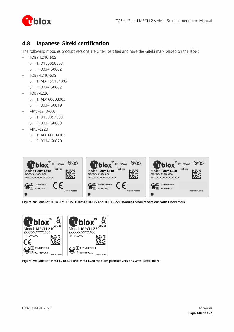
TOBY-L2 and MPCI-L2 series - System Integration Manual
UBX-13004618 - R25 Approvals
Page 148 of 162
4.8 Japanese Giteki certification
The following modules product versions are Giteki certified and have the Giteki mark placed on the label:
TOBY-L210-60S
o T: D150056003
o R: 003-150062
TOBY-L210-62S
o T: ADF150154003
o R: 003-150062
TOBY-L220
o T: AD160008003
o R: 003-160019
MPCI-L210-60S
o T: D150057003
o R: 003-150063
MPCI-L220
o T: AD160009003
o R: 003-160020
TOBY-L210
D150056003
003-150062
60S-xxTOBY-L220
AD160008003
003-160019
xxS-xxTOBY-L210
ADF150154003
003-150062
62S-xx
Figure 78: Label of TOBY-L210-60S, TOBY-L210-62S and TOBY-L220 modules product versions with Giteki mark
MPCI-L21060S-xx
D150057003
003-150063
MPCI-L220xxS-xx
AD160009003
003-160020
Figure 79: Label of MPCI-L210-60S and MPCI-L220 modules product versions with Giteki mark

TOBY-L2 and MPCI-L2 series - System Integration Manual
UBX-13004618 - R25 Product testing
Page 149 of 162
5 Product testing
5.1 u-blox in-series production test
u-blox focuses on high quality for its products. All units produced are fully tested automatically in production line. Stringent quality control process has been implemented in the production line. Defective units are analyzed in detail to improve the production quality.
This is achieved with automatic test equipment (ATE) in production line, which logs all production and measurement data. A detailed test report for each unit can be generated from the system. Figure 80 illustrates typical automatic test equipment (ATE) in a production line.
The following typical tests are among the production tests.
Digital self-test (firmware download, Flash firmware verification, IMEI programming)
Measurement of voltages and currents
Adjustment of ADC measurement interfaces
Functional tests (USB interface communication, SIM card communication)
Digital tests (GPIOs and other interfaces)
Measurement and calibration of RF characteristics in all supported bands (such as receiver S/N verification, frequency tuning of reference clock, calibration of transmitter and receiver power levels, etc.)
Verification of RF characteristics after calibration (i.e. modulation accuracy, power levels, spectrum, etc. are checked to ensure they are all within tolerances when calibration parameters are applied)
Figure 80: Automatic test equipment for module tests
TOBY-L2 and MPCI-L2 series - System Integration Manual
UBX-13004618 - R25 Product testing
Page 150 of 162
5.2 Test parameters for OEM manufacturer
Because of the testing done by u-blox (with 100% coverage), an OEM manufacturer does not need to repeat firmware tests or measurements of the module RF performance or tests over analog and digital interfaces in their production test.
However, an OEM manufacturer should focus on:
Module assembly on the device; it should be verified that:
o Soldering and handling process did not damage the module components
o All module pins are well soldered on device board
o There are no short circuits between pins
Component assembly on the device; it should be verified that:
o Communication with host controller can be established
o The interfaces between module and device are working
o Overall RF performance test of the device including antenna
Dedicated tests can be implemented to check the device. For example, the measurement of module current consumption when set in a specified status can detect a short circuit if compared with a “Golden Device” result.
In addition, module AT commands can be used to perform functional tests on digital interfaces (communication with host controller, check SIM interface, GPIOs, etc.), on audio interfaces (audio loop for test purposes can be enabled by the AT+UPAR=2 command as described in the u-blox AT Commands Manual [3]), and to perform RF performance tests (see the following section 5.2.2 for details).
5.2.1 “Go/No go” tests for integrated devices
A “Go/No go” test is typically to compare the signal quality with a “Golden Device” in a location with excellent network coverage and known signal quality. This test should be performed after data connection has been established. AT+CSQ is the typical AT command used to check signal quality in term of RSSI. See the u-blox AT Commands Manual [3] for detail usage of the AT command.
These kinds of test may be useful as a “go/no go” test but not for RF performance measurements.
This test is suitable to check the functionality of communication with host controller, SIM card as well as power supply. It is also a means to verify if components at antenna interface are well soldered.
5.2.2 RF functional tests
The overall RF functional test of the device including the antenna can be performed with basic instruments such as a spectrum analyzer (or an RF power meter) and a signal generator with the assistance of AT+UTEST command over AT command user interface.
The AT+UTEST command provides a simple interface to set the module to Rx or Tx test modes ignoring the LTE/3G/2G signaling protocol. The command can set the module into:
transmitting mode in a specified channel and power level in all supported modulation schemes and bands
receiving mode in a specified channel to returns the measured power level in all supported bands
See the u-blox AT Commands Manual [3] and the End user test Application Note [26], for the AT+UTEST command syntax description and detail guide of usage.
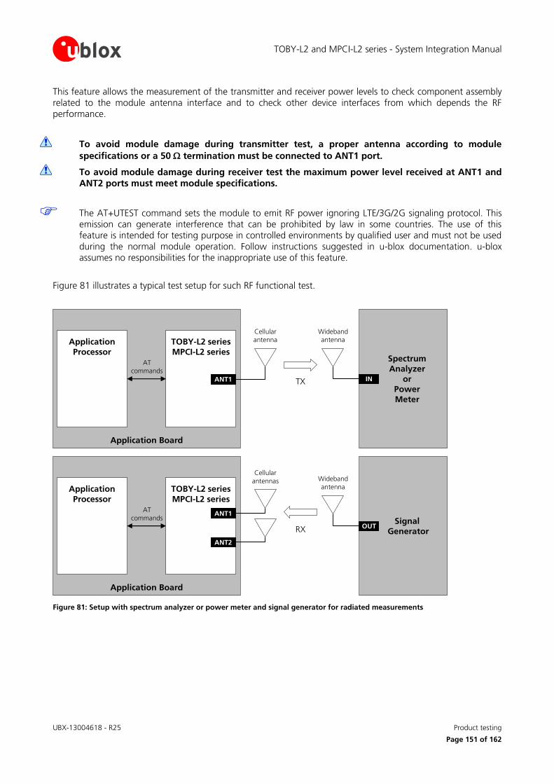
TOBY-L2 and MPCI-L2 series - System Integration Manual
UBX-13004618 - R25 Product testing
Page 151 of 162
This feature allows the measurement of the transmitter and receiver power levels to check component assembly related to the module antenna interface and to check other device interfaces from which depends the RF performance.
To avoid module damage during transmitter test, a proper antenna according to module
specifications or a 50 termination must be connected to ANT1 port.
To avoid module damage during receiver test the maximum power level received at ANT1 and ANT2 ports must meet module specifications.
The AT+UTEST command sets the module to emit RF power ignoring LTE/3G/2G signaling protocol. This emission can generate interference that can be prohibited by law in some countries. The use of this feature is intended for testing purpose in controlled environments by qualified user and must not be used during the normal module operation. Follow instructions suggested in u-blox documentation. u-blox assumes no responsibilities for the inappropriate use of this feature.
Figure 81 illustrates a typical test setup for such RF functional test.
Application Board
TOBY-L2 series
MPCI-L2 series
ANT1
Application
ProcessorAT
commands
Cellular
antenna
Spectrum
Analyzer
or
Power
Meter
IN
Wideband
antenna
TX
Application Board
TOBY-L2 series
MPCI-L2 series
ANT1
Application
ProcessorAT
commands
Cellular
antennas
Signal
GeneratorOUT
Wideband
antenna
RX
ANT2
Figure 81: Setup with spectrum analyzer or power meter and signal generator for radiated measurements
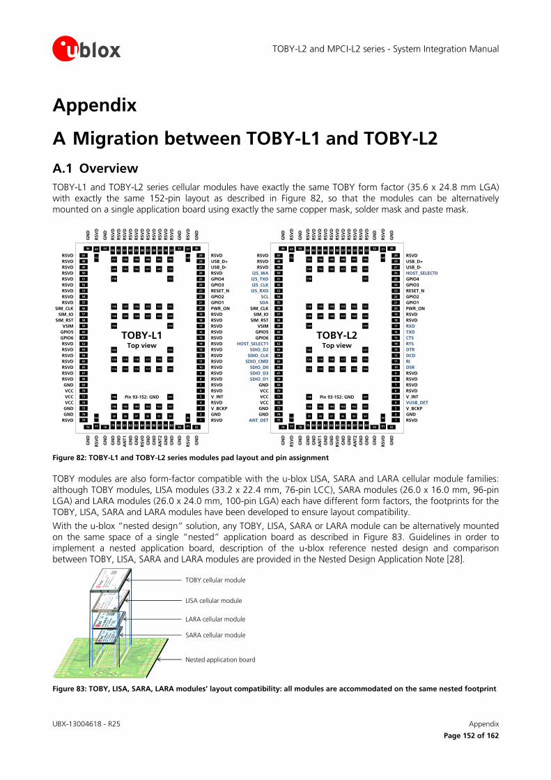
TOBY-L2 and MPCI-L2 series - System Integration Manual
UBX-13004618 - R25 Appendix
Page 152 of 162
Appendix
A Migration between TOBY-L1 and TOBY-L2
A.1 Overview
TOBY-L1 and TOBY-L2 series cellular modules have exactly the same TOBY form factor (35.6 x 24.8 mm LGA) with exactly the same 152-pin layout as described in Figure 82, so that the modules can be alternatively mounted on a single application board using exactly the same copper mask, solder mask and paste mask.
11
10
7
5
4
2
1
21
19
18
16
15
13
12
29
27
26
24
23
8
6
3
22
20
17
14
28
25
9
65
66
69
71
72
74
75
55
57
58
60
61
63
64
47
49
50
52
53
68
70
73
54
56
59
62
48
51
67
RSVD
RSVD
GND
VCC
VCC
GND
RSVD
RSVD
SIM_IO
SIM_RST
GPIO5
GPIO6
RSVD
RSVD
RSVD
RSVD
RSVD
RSVD
RSVD
RSVD
VCC
GND
RSVD
SIM_CLK
VSIM
RSVD
RSVD
RSVD
RSVD
RSVD
RSVD
RSVD
V_INT
RSVD
GND
RSVD
GPIO1
RSVD
RSVD
RSVD
RSVD
RSVD
RSVD
RSVD
USB_D-
RSVD
GPIO3
RESET_N
RSVD
RSVD
V_BCKP
GPIO2
PWR_ON
RSVD
RSVD
USB_D+
GPIO4
RSVD
90 91 92787776
93100
79 80 83 85 86 88 8982 84 8781
GN
D
RSV
D
GN
D
GN
D
RSV
D
GN
D
GN
D
GN
D
GN
D
GN
D
GN
D
GN
D
GN
D
GN
D
RSV
D
AN
T2
AN
T1
32 31 30444546
145152
43 42 39 37 36 34 3340 38 3541
GN
D
RSV
D
GN
D
GN
D
RSV
D
GN
D
RSV
D
RSV
D
RSV
D
RSV
D
RSV
D
RSV
D
RSV
D
RSV
D
RSV
D
RSV
D
RSV
D
99 98 97 96 95 94
106 105 104 103 102 101
108 107
124 123
130 129 128 127 126 125
136 135 134 133 132 131
138 137
144 143 142 141 140 139
151 150 149 148 147 146
114 113 112 111 110 109
120 119 118 117 116 115
122 121
Pin 93-152: GND
TOBY-L1Top view
11
10
7
5
4
2
1
21
19
18
16
15
13
12
29
27
26
24
23
8
6
3
22
20
17
14
28
25
9
65
66
69
71
72
74
75
55
57
58
60
61
63
64
47
49
50
52
53
68
70
73
54
56
59
62
48
51
67
SDIO_CMD
SDIO_D0
GND
VCC
VCC
GND
ANT_DET
SDA
SIM_IO
SIM_RST
GPIO5
GPIO6
SDIO_D2
SDIO_CLK
RSVD
RSVD
I2S_WA
I2S_CLK
I2S_RXD
SDIO_D1
VCC
GND
SCL
SIM_CLK
VSIM
HOST_SELECT1
RSVD
I2S_TXD
SDIO_D3
RI
DSR
RSVD
V_INT
VUSB_DET
GND
RSVD
GPIO1
RSVD
RSVD
TXD
CTS
DTR
DCD
RSVD
USB_D-
HOST_SELECT0
GPIO3
RESET_N
RSVD
RSVD
V_BCKP
GPIO2
PWR_ON
RXD
RTS
USB_D+
GPIO4
RSVD
90 91 92787776
93100
79 80 83 85 86 88 8982 84 8781
GN
D
RSV
D
GN
D
GN
D
RSV
D
GN
D
GN
D
GN
D
GN
D
GN
D
GN
D
GN
D
GN
D
GN
D
RSV
D
AN
T2
AN
T1
32 31 30444546
145152
43 42 39 37 36 34 3340 38 3541
GN
D
RSV
D
GN
D
GN
D
RSV
D
GN
D
RSV
D
RSV
D
RSV
D
RSV
D
RSV
D
RSV
D
RSV
D
RSV
D
RSV
D
RSV
D
RSV
D
99 98 97 96 95 94
106 105 104 103 102 101
108 107
124 123
130 129 128 127 126 125
136 135 134 133 132 131
138 137
144 143 142 141 140 139
151 150 149 148 147 146
114 113 112 111 110 109
120 119 118 117 116 115
122 121
Pin 93-152: GND
TOBY-L2Top view
Figure 82: TOBY-L1 and TOBY-L2 series modules pad layout and pin assignment
TOBY modules are also form-factor compatible with the u-blox LISA, SARA and LARA cellular module families: although TOBY modules, LISA modules (33.2 x 22.4 mm, 76-pin LCC), SARA modules (26.0 x 16.0 mm, 96-pin LGA) and LARA modules (26.0 x 24.0 mm, 100-pin LGA) each have different form factors, the footprints for the TOBY, LISA, SARA and LARA modules have been developed to ensure layout compatibility.
With the u-blox “nested design” solution, any TOBY, LISA, SARA or LARA module can be alternatively mounted on the same space of a single “nested” application board as described in Figure 83. Guidelines in order to implement a nested application board, description of the u-blox reference nested design and comparison between TOBY, LISA, SARA and LARA modules are provided in the Nested Design Application Note [28].
LISA cellular module
LARA cellular module
SARA cellular module
Nested application board
TOBY cellular module
Figure 83: TOBY, LISA, SARA, LARA modules’ layout compatibility: all modules are accommodated on the same nested footprint
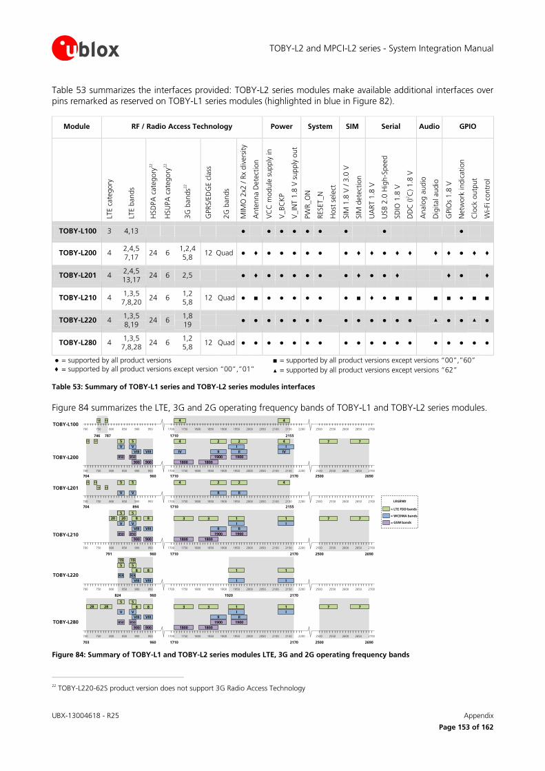
TOBY-L2 and MPCI-L2 series - System Integration Manual
UBX-13004618 - R25 Appendix
Page 153 of 162
Table 53 summarizes the interfaces provided: TOBY-L2 series modules make available additional interfaces over pins remarked as reserved on TOBY-L1 series modules (highlighted in blue in Figure 82).
Module RF / Radio Access Technology Power System SIM Serial Audio GPIO
LTE c
ate
gory
LTE b
ands
HSD
PA
cate
gory
22
HSU
PA
cate
gory
22
3G
bands2
2
GPRS/E
DG
E c
lass
2G
bands
MIM
O 2
x2 /
Rx
div
ers
ity
Ante
nna D
ete
ctio
n
VC
C m
odule
supp
ly in
V_BC
KP
V_IN
T 1
.8 V
supply
out
PW
R_O
N
RESET_N
Host
sele
ct
SIM
1.8
V / 3
.0 V
SIM
dete
ctio
n
UA
RT 1
.8 V
USB 2
.0 H
igh
-Speed
SD
IO 1
.8 V
DD
C (I2C
) 1.8
V
Analo
g a
udio
Dig
ital audio
GPIO
s 1.8
V
Netw
ork
indic
ation
Clo
ck o
utp
ut
Wi-
Fi c
ontr
ol
TOBY-L100 3 4,13 ● ● ● ● ● ● ● ● ●
TOBY-L200 4 2,4,5
7,17 24 6
1,2,4
5,8 12 Quad ● ♦ ● ● ● ● ● ● ♦ ♦ ● ♦ ♦ ♦ ♦ ● ♦ ♦
TOBY-L201 4 2,4,5 13,17
24 6 2,5 ● ♦ ● ● ● ● ● ● ♦ ● ● ♦ ♦ ● ♦
TOBY-L210 4 1,3,5
7,8,20 24 6
1,2 5,8
12 Quad ● ■ ● ● ● ● ● ● ■ ♦ ● ■ ■ ■ ■ ● ■ ■
TOBY-L220 4 1,3,5 8,19
24 6 1,8 19
● ● ● ● ● ● ● ● ● ● ● ● ● ▲ ● ● ▲ ●
TOBY-L280 4 1,3,5
7,8,28 24 6
1,2 5,8
12 Quad ● ● ● ● ● ● ● ● ● ● ● ● ● ● ● ● ● ●
● = supported by all product versions
♦ = supported by all product versions except version “00”,”01”
■ = supported by all product versions except versions “00”,”60”
▲ = supported by all product versions except versions “62”
Table 53: Summary of TOBY-L1 series and TOBY-L2 series modules interfaces
Figure 84 summarizes the LTE, 3G and 2G operating frequency bands of TOBY-L1 and TOBY-L2 series modules.
= WCDMA bands
= GSM bands
= LTE FDD bands
LEGEND
TOBY-L100
TOBY-L200
TOBY-L220
TOBY-L210
TOBY-L201
TOBY-L280
V
VIIIVIII
V
800 850 900 950
746 787
750700
704 960
800 850 900 950750700
1313
1717 55
850
900
850
900
800 850 900 950
824
750700
960
II II
II
IV IV
1700 1750 1800 1850 1900 1950 2000 2050 2100 2150
1710 2155
1710 2170
1700 1750 1800 1850 1900 1950 2000 2050 2100 2150
4 4
4 42 2
2200
2200
1800
1900 1900
1800
1700 1750 1800 1850 1900 1950 2000 2050 2100 2150
1920 2170
2500 2550 2600 2650 2700
2500 2690
2500 2550 2600 2650 2700
7 7
2500 2550 2600 2650 27002200
V
VIIIVIII
V
800 850 900 950
791
750
V
960
700
20 20
55
88
850
900
850
900
II II
II
1700 1750 1800 1850 1900 1950 2000 2050 2100 2150
1710 2170
3 3 11
2200
1800
1900 1900
1800
2500 2550 2600 2650 2700
2500 2690
7 7
VV
704
800 850 900 950750700
894
1717 55
1313
II II
1710
1700 1750 1800 1850 1900 1950 2000 2050 2100 2150
2155
4 42 2
2200 2500 2550 2600 2650 2700
V
VIIIVIII
V
800 850 900 950
703
750700
960
2828
55
88
850
900
850
900
II
II II
1700 1750 1800 1850 1900 1950 2000 2050 2100 2150
1710 2170
3 3 11
2500 2690
2500 2550 2600 2650 2700
7 7
2200
1800
1900 1900
1800
VIIIVIII
55
88
II
11
1919
XIXXIX
Figure 84: Summary of TOBY-L1 and TOBY-L2 series modules LTE, 3G and 2G operating frequency bands
22
TOBY-L220-62S product version does not support 3G Radio Access Technology
TOBY-L2 and MPCI-L2 series - System Integration Manual
UBX-13004618 - R25 Appendix
Page 154 of 162
A.2 Pin-out comparison between TOBY-L1 and TOBY-L2
TOBY-L1 TOBY-L2
Pin No Pin Name Description Pin Name Description Remarks for migration
1 RSVD Reserved RSVD Reserved
2 GND Ground GND Ground
3 V_BCKP RTC Supply Output
2.5 V output only
RTC backup function not available
V_BCKP RTC Supply Input/Output
3.0 V output
1.4 V – 4.2 V input (RTC backup)
RTC back-up: No Yes
4 RSVD Reserved VUSB_DET VBUS USB supply (5 V) detection23 No difference: leave unconnected
as reserved or not supported
5 V_INT Interfaces Supply Output
1.8 V output
V_INT Interfaces Supply Output
1.8 V output
No functional difference
6 RSVD Reserved RSVD Reserved
This pin must be connected to GND
No connect Connect to GND
7-9 RSVD Reserved RSVD Reserved
10 RSVD Reserved DSR UART DSR Output24 / GPIO
25 Reserved UART / GPIO
11 RSVD Reserved RI UART RI Output24 / GPIO
25 Reserved UART / GPIO
12 RSVD Reserved DCD UART DCD Output24 / GPIO
25 Reserved UART / GPIO
13 RSVD Reserved DTR UART DTR Input24 / GPIO
25 Reserved UART / GPIO
14 RSVD Reserved RTS UART RTS Input24 Reserved UART
15 RSVD Reserved CTS UART CTS Output24 Reserved UART
16 RSVD Reserved TXD UART Data Input24 Reserved UART
17 RSVD Reserved RXD UART Data Output24 Reserved UART
18-19 RSVD Reserved RSVD Reserved
20 PWR_ON Power-on Input
No internal pull-up
PWR_ON Power-on Input
Internal 50k pull-up to VCC
Pull-up: External Internal
21 GPIO1 GPIO26
WWAN status indication on “00” product version
GPIO1 GPIO25
WWAN status indication on ”00”, “01” and “60” product versions
No functional difference
22 GPIO2 GPIO26 GPIO2 GPIO
25
23 RESET_N Reset signal Input
Internal 10k pull-up to V_BCKP
Switch-off function only
RESET_N Reset signal Input
Internal 50k pull-up to VCC
Reset, Switch-on, Switch-off
Internal pull-up: V_BCKP VCC
Switch-off Reset, Switch-on/off
24 GPIO3 GPIO26 GPIO3 GPIO
25
25 GPIO4 GPIO26 GPIO4 GPIO
25
26 RSVD Reserved HOST_SELECT0 Input for selection of module configuration by the host
23
Reserved HOST_SELECT0
27 USB_D- USB Data I/O (D-) USB_D- USB Data I/O (D-) No functional difference
28 USB_D+ USB Data I/O (D+) USB_D+ USB Data I/O (D+) No functional difference
29 RSVD Reserved RSVD Reserved
30 GND Ground GND Ground
31 RSVD Reserved RSVD Reserved
32 GND Ground GND Ground
33-43 RSVD Reserved RSVD Reserved
44 GND Ground GND Ground
45 RSVD Reserved RSVD Reserved
46 GND Ground GND Ground
47-49 RSVD Reserved RSVD Reserved
50 RSVD Reserved I2S_WA I2S Word Alignment
27 / GPIO
25 Reserved I2S / GPIO
51 RSVD Reserved I2S_TXD I2S Data Output
27 / GPIO
25 Reserved I2S / GPIO
52 RSVD Reserved I2S_CLK I2S Clock
27 / GPIO
25 Reserved I2S / GPIO
53 RSVD Reserved I2S_RXD I2S Data Input
27 / GPIO
25 Reserved I2S / GPIO
23
Not supported by all product versions 24
Not supported by “00” product versions 25
Not supported by “00”, “01”, “60” product versions 26
Not supported by current product version 27
Not supported by “00”, “01”, “60”, TOBY-L201-02S, TOBY-L220-62S product versions
TOBY-L2 and MPCI-L2 series - System Integration Manual
UBX-13004618 - R25 Appendix
Page 155 of 162
TOBY-L1 TOBY-L2
Pin No Pin Name Description Pin Name Description Remarks for migration
54 RSVD Reserved SCL I2C Clock Output
28 Reserved I2C
55 RSVD Reserved SDA I2C Data I/O
28 Reserved I2C
56 SIM_CLK SIM Clock Output SIM_CLK SIM Clock Output No functional difference
57 SIM_IO SIM Data I/O SIM_IO SIM Data I/O No functional difference
58 SIM_RST SIM Reset Output SIM_RST SIM Reset Output No functional difference
59 VSIM SIM Supply Output VSIM SIM Supply Output No functional difference
60 GPIO5 GPIO29 GPIO5 GPIO
30
SIM detection
61 GPIO6 GPIO29 GPIO6 GPIO
30
62 RSVD Reserved HOST_SELECT1 Input for selection of module configuration by the host
31
Reserved HOST_SELECT1
63 RSVD Reserved SDIO_D2 SDIO serial data [2]30 Reserved SDIO
64 RSVD Reserved SDIO_CLK SDIO serial clock30 Reserved SDIO
65 RSVD Reserved SDIO_CMD SDIO command30 Reserved SDIO
66 RSVD Reserved SDIO_D0 SDIO serial data [0]30 Reserved SDIO
67 RSVD Reserved SDIO_D3 SDIO serial data [3]30 Reserved SDIO
68 RSVD Reserved SDIO_D1 SDIO serial data [1]30 Reserved SDIO
69 GND Ground GND Ground
70-72 VCC Module Supply Input
3.40 V – 4.50 V normal range
No 2G current pulses
No switch-on applying VCC
VCC Module Supply Input
3.40 V – 4.35 V normal range
High 2G current pulses
Switch-on applying VCC
No VCC functional difference
73-74 GND Ground GND Ground
75 RSVD Reserved ANT_DET Antenna Detection Input30 Reserved ANT_DET
76 GND Ground GND Ground
77 RSVD Reserved RSVD Reserved
78-80 GND Ground GND Ground
81 ANT1 RF Antenna Input/Output
Two LTE bands
No 3G bands
No 2G bands
ANT1 RF Antenna Input/Output
Up to six LTE bands
Up to five 3G bands
Four 2G bands
No RF functional difference
Different operating bands support
82-83 GND Ground GND Ground
84 RSVD Reserved RSVD Reserved
85-86 GND Ground GND Ground
87 ANT2 RF Antenna Input
LTE MIMO 2x2
No 3G Rx diversity
ANT2 RF Antenna Input
LTE MIMO 2x2
3G Rx diversity
No RF functional difference
Different operating bands support
88-90 GND Ground GND Ground
91 RSVD Reserved RSVD Reserved
92-152 GND Ground GND Ground
Table 54: TOBY-L1 and TOBY-L2 pin assignment with remarks for migration
28
Not supported by “00”, “01”, “60”, TOBY-L201-02S product versions 29
Not supported by current product version 30
Not supported by “00”, “01”, “60” product versions 31
Not supported by all product versions
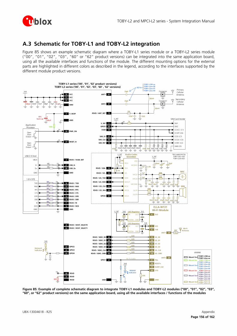
TOBY-L2 and MPCI-L2 series - System Integration Manual
UBX-13004618 - R25 Appendix
Page 156 of 162
A.3 Schematic for TOBY-L1 and TOBY-L2 integration
Figure 85 shows an example schematic diagram where a TOBY-L1 series module or a TOBY-L2 series module (“00”, “01”, “02”, “03”, “60” or “62” product versions) can be integrated into the same application board, using all the available interfaces and functions of the module. The different mounting options for the external parts are highlighted in different colors as described in the legend, according to the interfaces supported by the different module product versions.
3V8
GND330uF 100nF 10nF
71 VCC
72 VCC
70 VCC
3 V_BCKP
23 RESET_N
Application Processor
Open Drain
Output
20 PWR_ON
Open Drain
Output
68pF
TP
TP
15pF 8.2pF
+
100uF
+
GND
RTCback-up
16 RSVD / TXD
17 RSVD / RXD
12 RSVD / DCD
14 RSVD / RTS
15 RSVD / CTS
13 RSVD / DTR
10 RSVD / DSR
11 RSVD / RI
TP
TP
TP
TP
TP
TP
TP
TPTXD
RXD
DCD
RTS
CTS
DTR
DSR
RI
1.8 V DTE
GND GND
USB 2.0 Host
D-
D+
27 USB_D-
28 USB_D+
VBUS 4 RSVD / VUSB_DET
TP
TP
GND GND
0Ω
0Ω
0Ω
0Ω
0Ω
0Ω
0Ω
26 RSVD / HOST_SELECT0
62 RSVD / HOST_SELECT1
RSVD
RSVD
6
RSVD49TP
0Ω
100k
21GPIO1Wi-Fi enable
ELLA-W131
Wi-Fi Module
ANT1 29
ANT2 26
BPF
LDO Regulator3V8
OUTIN VIO5
1V86
LDO Regulator 3V33V8
OUTIN
GNDSHDNn
3V34
1V8
OUTIN
GNDSHDNn
V_INT
470k
65RSVD / SDIO_CMD
66RSVD / SDIO_D0
68RSVD / SDIO_D1
63RSVD / SDIO_D2
67RSVD / SDIO_D3
64RSVD / SDIO_CLK
22Ω
22Ω
22Ω
22Ω
22Ω
22Ω
SD_D015
SD_D116
SD_D211
SD_D312
SD_CLK14
SD_CMD13
GND
PDn9
RESETn10
SLEEP_CLK19
CFG20
GND
47k
Wi-Fi Antenna
3V8
WWAN Indicator
0Ω
0Ω
0Ω
TOBY-L1 series (’00’, ‘01’, ‘02’ product versions)
TOBY-L2 series (’00’, ‘01’, ’02’, ’03’, ‘60’ , ‘62’ versions)
47pF
SIM Card Holder
CCVCC (C1)
CCVPP (C6)
CCIO (C7)
CCCLK (C3)
CCRST (C2)
GND (C5)47pF 47pF 100nF
59VSIM
57SIM_IO
56SIM_CLK
58SIM_RST
47pF
SW1
SW2
5V_INT
60GPIO5
470k ESD ESD ESD ESD ESD ESD
1kTP
V_INT
V_INT
BCLK
LRCLK
Audio Codec MAX9860
SDIN
SDOUT
52RSVD / I2S_CLK
50RSVD / I2S_WA
51RSVD / I2S_TXD
53RSVD / I2S_RXD
61GPIO6 MCLK
10µF1µF100nF
VDD
SPK
OUTP
OUTN
MIC
MICBIAS
1µF
MICLN
MICLP
MICGND
EMI
EMI
EMI
EMI
1µF 2.2k
1µF
2.2k
ESD ESD10nF10nF 27pF27pF
10nF ESD ESD27pF27pF10nF
87ANT2
75RSVD / ANT_DET10k
Connector
27pF ESD
Secondary Cellular Antenna
33pF
82nH
82nH
81
ConnectorPrimary Cellular Antenna
33pF
ANT1
LEGEND
TOBY-L100-xxTOBY-L2xx-00TOBY-L2xx-01
TOBY-L2xx-60
Mount for
TOBY-L100-xxTOBY-L2xx-xx
Mount for
TOBY-L2xx-01TOBY-L2xx-x2 TOBY-L2xx-x3
TOBY-L2xx-60
Mount for
Mount for TOBY-L100-xx
Mount for TOBY-L2xx-xx
Mount for
0Ω for
TOBY-L100-xxTOBY-L2xx-00TOBY-L2xx-01
TOBY-L2xx-60
22 GPIO2
24 GPIO3
25 GPIO4
3V8
NetworkIndicator
RSVD / SDA
RSVD / SCL
55
54
SDA
SCL
IRQn
10k
V_INT
4.7k
4.7k
Not supported by TOBY-L201-02S TOBY-L220-62S
TOBY-L2xx-x2 TOBY-L2xx-x3
Figure 85: Example of complete schematic diagram to integrate TOBY-L1 modules and TOBY-L2 modules (“00”, “01”, “02”, “03”, “60”, or “62” product versions) on the same application board, using all the available interfaces / functions of the modules
TOBY-L2 and MPCI-L2 series - System Integration Manual
UBX-13004618 - R25 Appendix
Page 157 of 162
B Glossary
3GPP 3rd Generation Partnership Project
8-PSK 8 Phase-Shift Keying modulation
16QAM 16-state Quadrature Amplitude Modulation
64QAM 64-state Quadrature Amplitude Modulation
ACM Abstract Control Model
ADC Analog to Digital Converter
AP Application Processor
ASIC Application-Specific Integrated Circuit
AT AT Command Interpreter Software Subsystem, or attention
BAW Bulk Acoustic Wave
CSFB Circuit Switched Fall-Back
DC Direct Current
DCE Data Communication Equipment
DDC Display Data Channel interface
DL Down-Link (Reception)
DRX Discontinuous Reception
DSP Digital Signal Processing
DTE Data Terminal Equipment
ECM Ethernet networking Control Model
EDGE Enhanced Data rates for GSM Evolution
EMC Electro-Magnetic Compatibility
EMI Electro-Magnetic Interference
ESD Electro-Static Discharge
ESR Equivalent Series Resistance
E-UTRA Evolved Universal Terrestrial Radio Access
FDD Frequency Division Duplex
FEM Front End Module
FOAT Firmware Over AT commands
FOTA Firmware Over The Air
FTP File Transfer Protocol
FW Firmware
GND Ground
GNSS Global Navigation Satellite System
GPIO General Purpose Input Output
GPRS General Packet Radio Service
GPS Global Positioning System
HBM Human Body Model
HSIC High Speed Inter Chip
HSDPA High Speed Downlink Packet Access
HSUPA High Speed Uplink Packet Access
HTTP HyperText Transfer Protocol
HW Hardware
I/Q In phase and Quadrature
I2C Inter-Integrated Circuit interface
I2S Inter IC Sound interface
IP Internet Protocol
LDO Low-Dropout
LGA Land Grid Array
TOBY-L2 and MPCI-L2 series - System Integration Manual
UBX-13004618 - R25 Appendix
Page 158 of 162
LNA Low Noise Amplifier
LPDDR Low Power Double Data Rate synchronous dynamic RAM memory
LTE Long Term Evolution
M2M Machine-to-Machine
MBIM Mobile Broadband Interface Model
MIMO Multi-Input Multi-Output
N/A Not Applicable
N.A. Not Available
NCM Network Control Model
OEM Original Equipment Manufacturer device: an application device integrating a u-blox cellular module
OTA Over The Air
PA Power Amplifier
PCM Pulse Code Modulation
PCN / IN Product Change Notification / Information Note
PCS Personal Communications Service
PFM Pulse Frequency Modulation
PMU Power Management Unit
PWM Pulse Width Modulation
QPSK Quadrature Phase Shift Keying
RF Radio Frequency
RMII Reduced Media Independent Interface
RNDIS Remote Network Driver Interface Specification
RSE Radiated Spurious Emission
RTC Real Time Clock
SAW Surface Acoustic Wave
SDIO Secure Digital Input Output
SIM Subscriber Identification Module
SMS Short Message Service
SRF Self Resonant Frequency
SSL Secure Socket Layer
TBD To Be Defined
TCP Transmission Control Protocol
TDD Time Division Duplex
TDMA Time Division Multiple Access
TIS Total Isotropic Sensitivity
TP Test-Point
TRP Total Radiated Power
UART Universal Asynchronous Receiver-Transmitter
UDP User Datagram Protocol
UICC Universal Integrated Circuit Card
UL Up-Link (Transmission)
UMTS Universal Mobile Telecommunications System
USB Universal Serial Bus
VCO Voltage Controlled Oscillator
VoLTE Voice over LTE
VSWR Voltage Standing Wave Ratio
Wi-Fi Wireless Local Area Network (IEEE 802.11 short range radio technology)
WLAN Wireless Local Area Network (IEEE 802.11 short range radio technology)
WWAN Wireless Wide Area Network (GSM / UMTS / LTE cellular radio technology)
TOBY-L2 and MPCI-L2 series - System Integration Manual
UBX-13004618 - R25 Related documents
Page 159 of 162
Related documents [1] u-blox TOBY-L2 series Data Sheet, Docu No UBX-13004573
[2] u-blox MPCI-L2 series Data Sheet, Docu No UBX-13004749
[3] u-blox AT Commands Manual, Docu No UBX-13002752
[4] u-blox EVK-L2x User Guide, Docu No UBX-14000422
[5] u-blox Windows Embedded OS USB Driver Installation Application Note, Docu No UBX-14003263
[6] u-blox Firmware Update Application Note, Docu No UBX-13001845
[7] Universal Serial Bus Revision 2.0 specification, http://www.usb.org/developers/docs/usb20_docs/
[8] ITU-T Recommendation V.24 - 02-2000 - List of definitions for interchange circuits between Data Terminal Equipment (DTE) and Data Circuit-terminating Equipment (DCE), http://www.itu.int/rec/T-REC-V.24-200002-I/en
[9] 3GPP TS 27.007 - AT command set for User Equipment (UE)
[10] 3GPP TS 27.005 - Use of Data Terminal Equipment - Data Circuit terminating; Equipment (DTE - DCE) interface for Short Message Service (SMS) and Cell Broadcast Service (CBS)
[11] 3GPP TS 27.010 - Terminal Equipment to User Equipment (TE-UE) multiplexer protocol
[12] u-blox Mux Implementation Application Note, Docu No UBX-13001887
[13] I2C-bus specification and user manual - Rev. 5 - 9 October 2012 - NXP Semiconductors,
http://www.nxp.com/documents/user_manual/UM10204.pdf
[14] u-blox GNSS Implementation Application Note, Docu No UBX-13001849
[15] u-blox Wi-Fi / Cellular Integration Application Note, Docu No UBX-14003264
[16] PCI Express Mini Card Electromechanical Specification, Revision 2.0, April 21, 2012
[17] GSM Association TS.09 - Battery Life Measurement and Current Consumption Technique https://www.gsma.com/newsroom/wp-content/uploads//TS.09_v10.0.pdf
[18] CENELEC EN 61000-4-2 (2001): "Electromagnetic compatibility (EMC) – Part 4-2: Testing and measurement techniques – Electrostatic discharge immunity test".
[19] ETSI EN 301 489-1 - Electromagnetic compatibility and Radio spectrum Matters (ERM); EMC standard for radio equipment and services; Part 1: Common technical requirements
[20] ETSI EN 301 489-52 - Electromagnetic Compatibility (EMC) standard for radio equipment and services; Part 52: Specific conditions for Cellular Communication Mobile and portable (UE) radio and ancillary equipment
[21] 3GPP TS 51.010-2 - Technical Specification Group GSM/EDGE Radio Access Network; Mobile Station (MS) conformance specification; Part 2: Protocol Implementation Conformance Statement (PICS)
[22] 3GPP TS 34.121-2 - Technical Specification Group Radio Access Network; User Equipment (UE) conformance
specification; Radio transmission and reception (FDD); Part 2: Implementation Conformance Statement (ICS)
[23] 3GPP TS 36.521-1 - Evolved Universal Terrestrial Radio Access; User Equipment conformance specification; Radio transmission and reception; Part 1: Conformance Testing
[24] 3GPP TS 36.521-2 - Evolved Universal Terrestrial Radio Access (E-UTRA); User Equipment conformance specification; Radio transmission and reception; Part 2: Implementation Conformance Statement (ICS)
[25] 3GPP TS 36.523-2 - Evolved Universal Terrestrial Radio Access (E-UTRA) and Evolved Packet Core (EPC); User Equipment conformance specification; Part 2: Implementation Conformance Statement (ICS)
[26] u-blox End user test Application Note, Docu No UBX-13001922
[27] u-blox Package Information Guide, Docu No UBX-14001652
[28] u-blox Nested Design Application Note, Docu No UBX-16007243
[29] SIM Access Profile Interoperability Specification, http://www.bluetooth.org
Some of the above documents can be downloaded from u-blox web-site (http://www.u-blox.com/).
TOBY-L2 and MPCI-L2 series - System Integration Manual
UBX-13004618 - R25 Revision history
Page 160 of 162
Revision history Revision Date Name Comments
R01 20-Dec-2013 sses Initial release for TOBY-L2 series
R02 21-Mar-2014 sses Initial release including MPCI-L2 series
UART and GPIOs remarked as not supported by TOBY-L2x0-00S
R03 23-Jul-2014 sses Advance Information document status
Updated MPCI-L2 descriptions; USB description and design-in, including VUSB_DET pin previously RSVD; MPCI-L2 thickness and installation guidelines; MPCI-L2 power-off procedure; MPCI-L2 pins 3, 5, 44, 46 definition: Not Connected instead of GPI/GPO; GPIOs
definition and description
Additional design-in examples, minor corrections and improvements
R04 30-Sep-2014 lpah Updated FW version for Engineering Samples
Additional design-in and minor corrections
R05 28-Nov-2014 lpah / sses Changed status to Early Production Information
Updated VUSB_DET description and application circuits: the VUSB_DET functionality is not supported, and the pin should be left unconnected or it should not be driven high
Added maximum antenna gain requirements as per FCC RF radiation exposure limits
Corrected MPCI-L2 pinout; Additional design-in and minor corrections
R06 28-Jan-2015 sses Added description and design-in for TOBY-L2xx-50S, i.e. the “50” product version: updated UART, SDIO, GPIO sections
R07 29-May-2015 sses Added description and design-in for TOBY-L280-00S and TOBY-L201-01S: updated UART, FTP, HTTP, FOTA sections and any other applicable section
R08 21-Jul-2015 sses Document status reverted to Objective Specification.
Added description and design-in for TOBY-L200-02S, TOBY-L210-02S, MPCI-L200-02S,
and MPCI-L210-02S product versions.
R09 19-Aug-2015 sses Changed status to Early Production Information
Added description and design-in for TOBY-L210-60S, MPCI-L210-60S product versions.
R10 30-Sep-2015 sses Document status reverted to Advance Information
R11 04-Nov-2015 sses Document status reverted to Objective Specification.
Added description and design-in for TOBY-L220-02S, TOBY-L280-02S, MPCI-L280-02S
modules product versions. Removed description and design-in for TOBY-L2xx-50S, TOBY-L280-00S modules product versions.
R12 26-Nov-2015 lpah Document status updated to Early Production Information
R13 22-Dec-2015 sses Added description and design-in for MPCI-L201-01S product versions
R14 31-Mar-2016 sses Document status reverted to Advance Information
Added description and design-in for TOBY-L210-62S product versions.
Updated features planned for future product versions.
Updated module and UART behavior in case of +UPSV=2 and +UPSV=3.
Minor other corrections and description improvements.
R15 27-Apr-2016 lpah Document status updated to Production Information
R16 15-Jul-2016 sses Document status reverted to Objective Specification.
Added description and design-in for TOBY-L201-02S, MPCI-L201-02S product versions
R17 27-Sep-2016 sses Document status updated to Advance Information.
Updated support of some minor features in specific product versions.
R18 21-Oct-2016 lpah Document status updated to Early Production Information.
Extended document applicability to TOBY-L280-72S, MPCI-L220-02S, MPCI-L280-72S
R19 25-Nov-2016 lpah Extended document applicability to TOBY-L200-00S-01 / MPCI-L200-00S-01
Removed document applicability to TOBY-L280-72S, MPCI-L280-72S
R20 21-Dec-2016 lpah / sses "Disclosure restriction" replaces "Document status" on page 2 and document footer
Extended document applicability to TOBY-L200-02S-01, TOBY-L210-02S-01, TOBY-L280-02S-01, MPCI-L200-02S-01, MPCI-L210-02S-01 and MPCI-L280-02S-01
Updated support of some features in specific product versions.
TOBY-L2 and MPCI-L2 series - System Integration Manual
UBX-13004618 - R25 Revision history
Page 161 of 162
Revision Date Name Comments
R21 24-Apr-2017 lpah / sses Extended document applicability to TOBY-L200-62S, MPCI-L220-62S
R22 05-Jun-2017 lpah / sses Updated TOBY-L201-02S product status to Initial production status.
R23 26-Jun-2017 lpah / sses Extended document applicability to TOBY-L2, MPCI-L2 "03" product version
R24 27-Jul-2017 lpah Updated TOBY-L200-00S-01, MPCI-L200-00S-01, TOBY-L210-00S-00, MPCI-L210-00S-00, TOBY-L210-60S-01 product status to End Of Life.
R25 03-Jan-2018 lpah / sses Updated TOBY-L200-02S-01, MPCI-L200-02S-01, TOBY-L210-02S-01, MPCI-L210-02S-01, TOBY-L280-02S-01, MPCI-L280-02S-01 product status to End Of Life.
Updated VCC rising edge requirement to switch-on the module
TOBY-L2 and MPCI-L2 series - System Integration Manual
UBX-13004618 - R25 Contact
Page 162 of 162
Contact For complete contact information, visit us at http://www.u-blox.com/
u-blox Offices
North, Central and South America
u-blox America, Inc.
Phone: +1 703 483 3180 E-mail: [email protected]
Regional Office West Coast:
Phone: +1 408 573 3640 E-mail: [email protected]
Technical Support:
Phone: +1 703 483 3185 E-mail: [email protected]
Headquarters
Europe, Middle East, Africa
u-blox AG
Phone: +41 44 722 74 44 E-mail: [email protected] Support: [email protected]
Asia, Australia, Pacific
u-blox Singapore Pte. Ltd.
Phone: +65 6734 3811 E-mail: [email protected] Support: [email protected]
Regional Office Australia:
Phone: +61 2 8448 2016 E-mail: [email protected] Support: [email protected]
Regional Office China (Beijing):
Phone: +86 10 68 133 545 E-mail: [email protected] Support: [email protected]
Regional Office China (Chongqing):
Phone: +86 23 6815 1588 E-mail: [email protected] Support: [email protected]
Regional Office China (Shanghai):
Phone: +86 21 6090 4832 E-mail: [email protected] Support: [email protected]
Regional Office China (Shenzhen):
Phone: +86 755 8627 1083 E-mail: [email protected] Support: [email protected]
Regional Office India:
Phone: +91 80 4050 9200 E-mail: [email protected] Support: [email protected]
Regional Office Japan (Osaka):
Phone: +81 6 6941 3660 E-mail: [email protected] Support: [email protected]
Regional Office Japan (Tokyo):
Phone: +81 3 5775 3850 E-mail: [email protected] Support: [email protected]
Regional Office Korea:
Phone: +82 2 542 0861 E-mail: [email protected] Support: [email protected]
Regional Office Taiwan:
Phone: +886 2 2657 1090 E-mail: [email protected] Support: [email protected]