Embed Size (px)
Citation preview

Journal of Solid State Chemistry 164, 188}200 (2002)
doi:10.1006/jssc.2001.9457, available online at http://www.idealibrary.com on
Defect Analysis of Ionically Compensated Quadruple and QuintuplePerovskite Layered Cuprates with Ti Blocking Layers
N. Mansourian-Hadavi,��* T. O. Mason,* D. Ko,? and K. R. Poeppelmeier-*Materials Science and Engineering Department, Northwestern University, 2225 North Campus Drive, Evanston, Illinois 60208-3108; -Department of
Chemistry, Northwestern University, Evanston, Illinois, 60208-3113; and ?Technology Development Center, Rubicon Technology Inc.,3000 Lakeside Drive, Suite 105N, Bannockburn, Illinois 60015
Received July 17, 2001; accepted November 16, 2001; published online February 1, 2002
This work presents a modi5ed defect model for pure andchemically substituted quadruple and quintuple pure perovskitelayered cuprates, using data from the Jonker (thermopower vs lnconductivity) and Brouwer (log conductivity vs log pO2) analyses.The closely matched in-plane bond lengths of the blocking andthe active layers in these structures promote ionic compensationrather than electronic compensation upon aliovalent p-type dop-ing. A comprehensive defect model that takes into account all themajor defect species in an ionically compensated quadruple orquintuple perovskite provides a better means for understandingthe electrical behavior of these novel materials. The presentedmodel allows for the calculation of e4ective dopant and theoxygen interstitial concentrations in these materials. � 2002
Elsevier Science (USA)
INTRODUCTION
Quadruple and quintuple perovskite layered cuprates arenovel members of the layered cuprate family of compounds.Because they have in common with high-¹
�superconduc-
tors certain structural features (e.g., 2D copper}oxygensheets), they have been extensively studied. In particular, thedefect chemistry of layered cuprates is of interest insofar asdoping/carrier generation mechanisms are concerned (1}9).Carrier generation is a necessary, but not su$cient, step forachieving high-T
�superconductivity. Previous point defect
models for layered cuprates are overly simpli"ed, and donot appropriately account for the high degree of ionic com-pensation that takes place in quadruple and quintuple per-ovskite cuprates. The present work develops an improvedmodel and applies it to the analysis of high-temperatureelectrical conductivity and thermopower data in a variety ofpure and chemically substituted copper-based quadrupleand quintuple perovskites.
�To whom correspondence should be addressed. Fax: 847-491-7820.E-mail: [email protected].
1880022-4596/02 $35.00� 2002 Elsevier Science (USA)All rights reserved.
Quadruple and quintuple perovskite layered cuprateshave double copper}oxygen planes (conducting layer) thatare separated by two and three titanate perovskite layers(blocking layer), respectively. A "xed valence and coordina-tion-preferring B-cation (e.g., Ti) provides minimal non-stoichiometry in the compounds. They primarily control thedoping of the CuO
�planes by imparting the proper strain
(i.e., compressive or tensile) through bond mismatch. Good-enough and Manthiram stressed the importance of the bondlength mismatch between the blocking and conductinglayers for doping in layered cuprate superconductors (10).The simple schematic in Fig. 1 expresses the bond mismatchidea by comparing the unrelaxed bond lengths of blockingand active layers of common high-¹
�layered cuprates with
di!erent coordination environments by using Shannon'sanion and cation radii (11). In p-type superconductors,blocking layers have shorter in-plane bond lengths than theconducting layers since Cu has 5- or 6-fold coordination,with a longer natural Cu}O distance than the M}O(M"La, Tl, Hg, etc.) distance in the blocking layer.La
�CuO
�is an example of such structures that combines
La(VI)}O blocking layers (r&1.84 A� ) with Cu(VI)}O(r&2.13 A� ) conducting layers. This clearly imparts acompressive strain to the conducting layers as a result of thebond mismatch. On the other hand, in the n-type supercon-ductor, (Nd,Ce)
�CuO
���, a Nd}O blocking layer(r&2.04 A� ) is stacked with a Cu(IV)}O conducting layer(r&1.95 A� ) which imparts a tensile strain to conductinglayers. However, structures with Ti}O (perovskite) andCu(V)}O (e.g., quadruple perovskite layered cuprate¸n
�Ba
�Cu
�Ti
�O
��) do not have as much bond length
di!erences, resulting in a bond-matched structure. Thein-plane bond length for p-type superconductors rangesfrom 1.90 A� to 1.938 A� and for n-type superconductorsfrom 1.96 to 1.98 A� leaving a so-called &&neutral'' region(r����
"1.938}1.965 A� ) in between for bond-matchedmaterials such as quadruple and quintuple layered cuprateperovskites.

FIG. 1. Schematic presentation for comparison of unrelaxed bond lengths of active and blocking layers of layered cuprate superconductors, usingShannon ionic radii (2) and the range of in-plane bond lengths for p- and n-type high-¹
�superconductors as well as quadruple and quintuple perovskite
layered cuprates.
189DEFECT ANALYSIS OF PEROVSKITE LAYERED CUPRATES
The most important feature of the blocking layer, the"xed oxygen stoichiometry, allows investigation of the ac-tive layer properties across a series, since the in-plane bondlength in the active layer varies with the composition of theblocking layer. Aliovalent doping in a p-type layered cu-prate perovskite results in the oxidation of copper in theconducting layer. Acceptor doping of the blocking layer ina compressive structure stabilizes holes while donor dopingof the blocking layer in a tensile structure stabilizes elec-trons in the conducting layer. The extent of aliovalent dop-ing in the blocking layer of a layered cuprate compounddepends primarily on the relative host and substituentcationic sizes. The materials with in-plane M}O distance intheir blocking layer very close to the in-plane Cu}Odistance in their conducting layer do not have the necessarydriving force (i.e., strain) in their structure to create signi"-cant carrier concentration (e.g., ¸n
�Ba
�Cu
�Ti
�O
��). There-
fore, aliovalent doping in the bond-matched quadruple andquintuple layered cuprate perovskite compounds results inionic compensation rather than electronic compensation.However, appropriate p-type substitution in A- and B-sitesproduces shorter in-plane bond lengths.
Because there are several major defect reactions going onin an aliovalently doped quadruple or quintuple perovskite,a defect model that considers multiple defect regimes allowsfor better understanding of the defect behavior of the com-pound. Such a defect model reveals the dominant defectreaction, providing information on the e!ective dopant
level. Oxygen defects are the most common types of defectsin the layered cuprate structures. Therefore, the oxygencontent of a layered cuprate perovskite can be an indicationof its defect concentration. A layered cuprate perovskitewith oxygen-de"cient blocking or active layers has oxygenvacancies that may or may not be re"llable upon sub-sequent annealing. For example, B-site acceptor doping inLa
�Ba
�Cu
���Ti
���O
���� results in oxygen vacancies in theblocking layer according to
CuO#Ti���
#O��
PCu����
#V ��
�#TiO
�. [1]
Re"lling these vacancies introduces holes back to thesystem:
12
O�
(g)#V��
�PO�
�#2h� . [2]
The other recognized oxygen defect reaction in layeredcuprates is the formation of oxygen interstitials,
12
O�(g)PO��
�#2h� , [3]
which should increase the hole content. However, theformation of oxygen interstitials between adjacent Cu}Osheets is believed to destroy the structural role of thesesheets in conductivity (12), although it increases hole con-centration and introduces some metallic behavior to thesemiconductor.
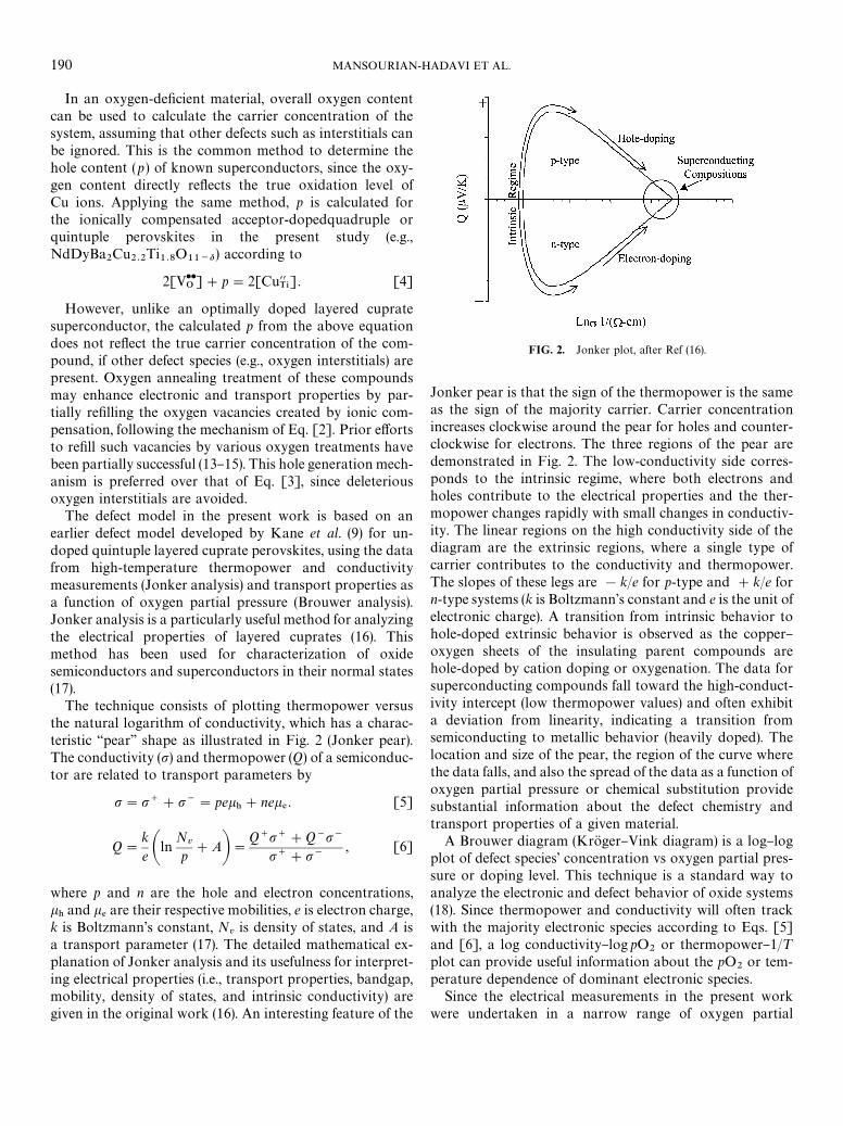
FIG. 2. Jonker plot, after Ref (16).
190 MANSOURIAN-HADAVI ET AL.
In an oxygen-de"cient material, overall oxygen contentcan be used to calculate the carrier concentration of thesystem, assuming that other defects such as interstitials canbe ignored. This is the common method to determine thehole content (p ) of known superconductors, since the oxy-gen content directly re#ects the true oxidation level ofCu ions. Applying the same method, p is calculated forthe ionically compensated acceptor-dopedquadruple orquintuple perovskites in the present study (e.g.,NdDyBa
�Cu
��Ti
�O
����) according to
2[V��
�]#p"2[Cu��
��]. [4]
However, unlike an optimally doped layered cupratesuperconductor, the calculated p from the above equationdoes not re#ect the true carrier concentration of the com-pound, if other defect species (e.g., oxygen interstitials) arepresent. Oxygen annealing treatment of these compoundsmay enhance electronic and transport properties by par-tially re"lling the oxygen vacancies created by ionic com-pensation, following the mechanism of Eq. [2]. Prior e!ortsto re"ll such vacancies by various oxygen treatments havebeen partially successful (13}15). This hole generation mech-anism is preferred over that of Eq. [3], since deleteriousoxygen interstitials are avoided.
The defect model in the present work is based on anearlier defect model developed by Kane et al. (9) for un-doped quintuple layered cuprate perovskites, using the datafrom high-temperature thermopower and conductivitymeasurements (Jonker analysis) and transport properties asa function of oxygen partial pressure (Brouwer analysis).Jonker analysis is a particularly useful method for analyzingthe electrical properties of layered cuprates (16). Thismethod has been used for characterization of oxidesemiconductors and superconductors in their normal states(17).
The technique consists of plotting thermopower versusthe natural logarithm of conductivity, which has a charac-teristic &&pear'' shape as illustrated in Fig. 2 (Jonker pear).The conductivity (�) and thermopower (Q) of a semiconduc-tor are related to transport parameters by
�"��#��"pe��#ne�
�. [5]
Q"
ke �ln
N�
p#A�"
Q���#Q���
��#��, [6]
where p and n are the hole and electron concentrations,��
and ��
are their respective mobilities, e is electron charge,k is Boltzmann's constant, N
�is density of states, and A is
a transport parameter (17). The detailed mathematical ex-planation of Jonker analysis and its usefulness for interpret-ing electrical properties (i.e., transport properties, bandgap,mobility, density of states, and intrinsic conductivity) aregiven in the original work (16). An interesting feature of the
Jonker pear is that the sign of the thermopower is the sameas the sign of the majority carrier. Carrier concentrationincreases clockwise around the pear for holes and counter-clockwise for electrons. The three regions of the pear aredemonstrated in Fig. 2. The low-conductivity side corres-ponds to the intrinsic regime, where both electrons andholes contribute to the electrical properties and the ther-mopower changes rapidly with small changes in conductiv-ity. The linear regions on the high conductivity side of thediagram are the extrinsic regions, where a single type ofcarrier contributes to the conductivity and thermopower.The slopes of these legs are !k/e for p-type and #k/e forn-type systems (k is Boltzmann's constant and e is the unit ofelectronic charge). A transition from intrinsic behavior tohole-doped extrinsic behavior is observed as the copper}oxygen sheets of the insulating parent compounds arehole-doped by cation doping or oxygenation. The data forsuperconducting compounds fall toward the high-conduct-ivity intercept (low thermopower values) and often exhibita deviation from linearity, indicating a transition fromsemiconducting to metallic behavior (heavily doped). Thelocation and size of the pear, the region of the curve wherethe data falls, and also the spread of the data as a function ofoxygen partial pressure or chemical substitution providesubstantial information about the defect chemistry andtransport properties of a given material.
A Brouwer diagram (KroK ger}Vink diagram) is a log}logplot of defect species' concentration vs oxygen partial pres-sure or doping level. This technique is a standard way toanalyze the electronic and defect behavior of oxide systems(18). Since thermopower and conductivity will often trackwith the majority electronic species according to Eqs. [5]and [6], a log conductivity}logpO
�or thermopower}1/¹
plot can provide useful information about the pO�
or tem-perature dependence of dominant electronic species.
Since the electrical measurements in the present workwere undertaken in a narrow range of oxygen partial

191DEFECT ANALYSIS OF PEROVSKITE LAYERED CUPRATES
pressure (10��}1 atm), it was not possible to plot a completeBrouwer diagram that covers all the di!erent defect regimes.However, log conductivity}logpO
�plots for oxide mater-
ials in this work can exhibit prevailing defect regimes underthe experimental conditions.
The majority of defect reactions in layered cuprate perov-skites are the ones that create oxygen interstitials or va-cancies. In the p-type oxides, oxygen interstitials and electronholes are the dominant ones as proposed by Hong (19),
12
O�(g) � O��
�#2h� [7]
K��
"
[O���]P�
PO����
[8]
under the electroneutrality condition
p"2[O���]"(2K
��)�� PO
���� . [9]
This result indicates a positive slope of 1/6 on a log �}log pO
�curve.
EXPERIMENTAL
Samples were prepared, corresponding to thestoichiometry NdDy
���(Sr,Ca)
�Ba
���Sr
�Cu
���Ti
���O
����,LaY
���Ca
�Ba
���Sr
�Cu
���Ti
���O
���� (quadruple perov-skite) and the stoichiometry NdDyCaBa
���Sr
�Cu
���Ti
��O
���� (quintuple perovskites). Typically 4}5 grams ofsamples were prepared by solid state reaction ofstoichiometric amounts of ¸n
�O
(¸n"Nd, Dy, La, Y),
ACO
(A"Ba, Sr, Ca), CuO, and TiO�, all of purity above
99.99%, using a Sartorius balance (Brinkmann Instrument,Westbury, NY) with $0.1 mg accuracy. The reagents wereground with a mortar and pestle, and "red in high-densityalumina crucibles at 9503C in air for 1 day in order toremove carbonates. Each sample was then ground andpressed at &2 MPa into pellets 12.5 millimeters diameterand 3}5 millimeters thick. The pellets were then "red at1030}10503C over the course of a 5}7-day reaction period,with several intermittent regrindings.
The phase purity of the air-quenched polycrystalline sam-ples was determined by X-ray powder di!raction ona Rigaku di!ractometer with Ni-"ltered CuK� radiation.Data were collected from 103 to 803 2� with a step size of0.053 and a collection time of 2 seconds at each step. Siliconwas used as an internal standard. Lattice parameters weredetermined by pattern matching [Le Bail "tting (20)] basedon a tetragonal unit cell (P4/mmm). The "tting was madewith the GSAS program (21).
To determine the oxygen stoichiometry and average cop-per valence in the samples, hydrogen reduction thermog-ravimetry was performed (TA Instrument 2950, New Castle,DE). Oxygen annealing of the samples was performed priorto TGA analysis, by equilibrating in #owing oxygen at
9003C and then slowly cooling to room temperature((13C/min) to facilitate oxygen trapping in the oxide struc-ture. For TGA runs, samples were preheated at 1203C for2 hours to remove any possible moisture. They were thenheated to 9003C at the rate of 53C/min, isothermally main-tained for 10 hours, and then cooled to room temperature.The whole process was carried out in a 7% H
�/N
�mixture
to achieve the desired reduction.Simultaneous four-point DC conductivity and Seebeck
coe$cient measurements, at temperatures from 800 to6503C, were performed using the technique described pre-viously (22, 23). Rectangular bar-shaped samples(3mm�3mm�9mm) were cut from sintered pellets andplaced between Au foils, the outer electrodes for electricalmeasurements, with auxiliary Au wire electrode contacts at&�
and &�
positions along each bar. A Pt and Pt/Rh
thermocouple (type S) was placed in contact with each of thefour electrodes along the bar. Samples were equilibrated inoxygen partial pressures ranging from 10�� atm to 1 atmusing oxygen or oxygen}argon premixtures. Measurementswere taken after equilibrium had been achieved (6}10hours). Conductivity/thermopower data were also takenduring slow-cooling over the temperature range, 800 to4003C, under #owing pure oxygen at a cooling rate of203C/hour. The measured conductivities were corrected forthe porosity of the samples according to the asymmetricmedium equation in the work of McLachlan et al. (relativedensity of 70%}75%) (24).
RESULTS AND DISSCUSION
The previous studies on several quadruple and quintupleperovskites layered cuprates (NdDyBa
���Sr
�Cu
���Ti
���O
���� , LaY���
Ca�Ba
�Cu
���Ti
���O
���� , andNdDyCaBa
���Sr
�Cu
���Ti
��O
����) elucidated theirunique electrical properties and defect chemistry ofthese materials (9, 15, 25). The new A- and B-sitedoped NdDy
���(Ca,Sr)
�Ba
���Sr
�Cu
���Ti
���O
���� andLaY
���Ca
�Ba
�Cu
���Ti
���O
���� quadruple compoundswere prepared based upon promising propertiesof these families of material (bond lengths,conductivity, and thermopower) in prior work (15). X-raydi!raction analysis detected no impurity phases inNdDy
���Sr
�Ba
�Cu
���Ti
���O
���� for 04z40.2 and04y40.2, LaY
���Ca
�Ba
�Cu
�Ti
�O
���� for 04x40.5,LaY
���Ca
�Ba
�Cu
��Ti
�O
���� for 04x40.3, andNdDy
��Ca
��Ba
��Sr
��Cu
��Ti
�O
���� . Employing thesmall}large A�A�� cation combination such as Nd and Dy orLa and Y in these quadruple compounds is a strategy toprevent the incorporation of oxygen defect species betweenadjacent copper}oxygen layers (25, 26). This design reducesthe spacing between adjacent Cu}O layers, making oxygenintercalation energetically unfavorable. A- and B-sitealiovalent codoping ([Sr�
��], [Ca�
�], [Cu��
��]) was the primary

FIG. 3. Jonker plots for quadruple perovskites at 7003C. Oxygenpartial pressures increase clockwise around the pear at values of 10��,10��, 10� , 10��, 10��, and 1 atm.
192 MANSOURIAN-HADAVI ET AL.
strategy to increase the hole concentration of the systems.Low-temperature resistivity measurements showed, how-ever, no superconducting transition in these quadruplecompounds.
TABLE 1Lattice Parameters for NdDy1�z (Sr,Ca)zBa2�xSrxCu2�y
Ti2�y O11�� Quadruple Compounds, Re5ned by GSAS Program
Compound a (A� ) c (A� )
NdDy��
Sr��
Ba�Cu
�Ti
�O
���� 3.8898$0.0004 15.690$0.002NdDy
�Sr
��Ba
�Cu
�Ti
�O
���� 3.8948$0.0003 15.701$0.001NdDy
��Sr
� Ba
�Cu
�Ti
�O
���� 3.8946$0.0004 15.678$0.002NdDy
��Sr
��Ba
�Cu
�Ti
�O
���� 3.9002$0.0005 15.679$0.002NdDy
�Sr
��Ba
�Cu
��Ti
�O
���� 3.8953$0.0004 15.692$0.002NdDy
��Sr
� Ba
�Cu
��Ti
�O
���� 3.8956$0.0003 15.693$0.001NdDy
�Sr
��Ba
��Sr
��Cu
��Ti
�O
���� 3.8977$0.0005 15.659$0.001NdDy
��Ca
��Ba
��Sr
��Cu
��Ti
�O
���� 3.9002$0.0002 15.725$0.003LaYCaBa
�Cu
��Ti
�O
���� 3.9010$0.0005 15.705$0.005LaY
��Ca
��Ba
�Cu
�Ti
�O
���� 3.8971$0.0008 15.702$0.003LaY
�Ca
��Ba
�Cu
�Ti
�O
���� 3.8961$0.0002 15.703$0.001LaY
��Ca
� Ba
�Cu
�Ti
�O
���� 3.8982$0.0003 15.706$0.001LaY
��Ca
��Ba
�Cu
�Ti
�O
���� 3.9011$0.0003 15.704$0.002LaY
��Ca
��Ba
�Cu
�Ti
�O
���� 3.9039$0.0004 15.709$0.002
The in-plane bond lengths of these compounds (Table 1)fall in the neutral region of Fig. 1. Therefore, the bond-matched character of their structure provides no drivingforce for the formation of carriers as a strain reliever. Sucha behavior leads to a low carrier concentration (see below),because ionic compensation becomes the dominant com-pensation mechanism as opposed to the desired electroniccompensation.
Thermogravimetric Analysis
The oxygen contents of the oxygen-annealed NdDyBa���
Sr�Cu
���Ti
���O
���� and LaY���
Ca�Ba
�Cu
���Ti
���O
����quadruple perovskite samples were measured using TGAanalysis (Table 2). The TGA-derived hole content (p�) inTable 2 is calculated according to Eq. [4] based on thecommon method used to derive the oxidation level of Cu inknown layered cuprate superconductors, as discussed be-fore. In other words, if we assume that oxygen interstitialsare not present in signi"cant concentration, the oxygencontent should be representative of the carrier concentra-tion. For example, �"0.2 (oxygen content"10.8) inNdDyBa
���Sr
�Cu
��Ti
�O
���� corresponds to strictlydivalent copper, which is the result of ionic rather thanelectronic compensation. Larger oxygen contents (smaller �)for x'0 suggest that the smaller Sr substituted for Ba ionmay make oxygen vacancy re"lling easier (15). However, inthese B-site doped quadruple compounds, where ionic com-pensation dominates, most of the acceptor species, [Cu��
��],
exist in neutral associates of [(Cu����
V��
�)�]; only the residual
are e!ective hole dopants. Hence, the calculation of holecontent using Eq. [4] overestimates the carrier content ofquadruple perovskites with Ti blocking layers. Later, wewill introduce a modi"ed defect model for these compoundsthat provides a more accurate estimation of Cu oxidationlevel. Therefore, the &&TGA-derived hole content'' (p�) is usedin this paper to distinguish the estimated hole content usingthe oxygen content (Eq. [4]) vs the estimated hole contentconsidering the overall defect chemistry (p ), as describedbelow.
High-Temperature Electrical Characterization
Jonker analysis for the NdDy���
(Sr, Ca)�Ba
���Sr
�Cu
���Ti
���O
���� and LaY���
Ca�Ba
�Cu
���Ti
���O
����samples was performed over a range of temperatures andoxygen partial pressures. Figure 3 shows the upper half ofthe Jonker pear for LaY
��Ca
� Ba
�Cu
�Ti
�O
����NdDy
�Sr
��Ba
�Cu
��Ti
�O
���� , and NdDy��
Ca��
Ba��
Sr��
Cu��
Ti�
O���� along with the Jonker plot of
NdDyBa��
Sr��
Cu��
Ti�
O���� for comparison purposes.
The plots for the A-site doped and A- and B-site codopedquadruple samples in Fig. 3 suggest improvement in electri-cal properties of the systems upon co-doping, as compared

TABLE 2Oxygen content for NdDy1�zSrzBa2Cu2�yTi2�yO11�� Quadruple Compounds from TGA Analysis
(Hole Contents Are Calculated per Copper Atom)
Compound Oxygen contentTGA-derived
hole content (p�)Oxygen annealed/air
quenched
NdDy��
Sr��
Ba�Cu
�Ti
�O
���� 11.01$0.02 0.10 Oxygen annealedNdDy
�Sr
��Ba
�Cu
�Ti
�O
���� 10.96$0.02 0.12 Oxygen annealedNdDy
��Sr
� Ba
�Cu
�Ti
�O
���� 10.92$0.02 0.14 Oxygen annealedNdDy
��Sr
��Ba
�Cu
�Ti
�O
���� 10.89$0.02 0.18 Oxygen annealedNdDy
�Sr
��Ba
�Cu
��Ti
�O
���� 10.81$0.02 0.22 Air quenchedNdDy
��Sr
� Ba
�Cu
��Ti
�O
���� 10.78$0.02 0.26 Oxygen annealedNdDy
�Sr
��Ba
��Sr
��Cu
��Ti
�O
���� 1078$0.02 0.07 Oxygen annealedLaYBa
�Cu
�Ti
�O
���� 11.01$0.02 0.0 Oxygen AnnealedLaYCaBa
�Cu
��Ti
�O
���� 10.77$0.10 0.0 Air quenchedLaY
���Ca
���Ba
�Cu
�Ti
�O
���� 11.02$0.02 0.09 Oxygen annealedLaY
��Ca
��Ba
�Cu
�Ti
�O
���� 10.99$0.02 0.040 Oxygen annealedLaY
�Ca
��Ba
�Cu
�Ti
�O
���� 10.99$0.02 0.095 Oxygen annealedLaY
��Ca
� Ba
�Cu
�Ti
�O
���� 10.97$0.02 0.120 Oxygen annealedLaY
��Ca
��Ba
�Cu
�Ti
�O
���� 10.88$0.02 0.085 Oxygen annealedLaY
��Ca
��Ba
�Cu
�Ti
�O
���� 10.87$0.02 0.116 Oxygen annealed
193DEFECT ANALYSIS OF PEROVSKITE LAYERED CUPRATES
to the B-site doped NdDyBa��
Sr��
Cu��
Ti�
O���� and
LaYBa�Cu
��Ti
�O
���� quadruple compounds character-ized in previous work (i.e., lower thermopower values andslightly higher �
�intercept) (15, 25). The relatively large
values of the conductivity data (��
) imply that either thedensity of states near the Fermi level and/or the carriermobility is enhanced. The fact that data for the A and B-sitedoped systems falls more toward the extrinsic leg of the plotcompared to that of parent compounds from previous workimplies an increased hole content of the system (25).
The slow-cooling plots for the same codoped compoundsare shown in Fig. 4 and exhibit thermopower values veryclose to the threshold of superconductivity (&43 �V/K).
FIG. 4. Simultaneous thermopower}conductivity measurements onslow-cooled quadruple samples at 203C/hour rate from +8003C to 4003Cunder #owing oxygen.
Semiconducting-to-metallic transition behavior (i.e., devi-ation of the data from the !k/e slope expected for semicon-ductors) is also observed. The higher �
�intercept of the
NdDy��
Ca��
Ba��
Sr��
Cu��
Ti�
O���� compound, com-
pared to the best B-site-only doped sample, NdDyBa��
Sr��
Cu��
Ti�
O����, indicates enhanced electrical and
transport properties.
Brouwer Analysis
The log � vs log pO�
plot (at 7003C) for the NdDy��
Ca��
Ba��
Sr��
Cu��
Ti�
O���� , NdDy
�Sr
��Ba
�Cu
��Ti
�O
���� , and LaY��
Ca�
Ba�Cu
�Ti
�O
���� samples,
FIG. 5. Brouwer plot of log �}log pO�
for quadruple perovskitesat 7003C.

FIG. 6. Plot of log �}log pO�
for NdDyCaBa���
Sr�Cu
��Ti
�O
����quintuple perovskite compound at 7003C.
194 MANSOURIAN-HADAVI ET AL.
along with the NdDyBa��
Sr��
Cu��
Ti�
O���� sample as
reference from previous work (15) in Fig. 5, indicates a verysmall pO
�dependence of conductivity for the LaY quadru-
ple compound (&1/14) compared to the rest of the NdDyquadruples with &1/8 slopes. This plot shows that theNdDy
��Ca
��Ba
��Sr
��Cu
��Ti
�O
���� sample has thehighest � of all the samples. A Brouwer plot forNdDyCaBa
���Sr
�Cu
���Ti
��O
���� (x"0, 0.1, 0.5) quin-tuple perovskite compounds using data in previous work(15) is presented in Fig. 6.
The expected slope in log �}log pO�
plots of the quadru-ple and quintuple perovskite systems due to oxygen inter-stitials as the dominant ionic defect and holes as the majorcharge carriers (Eq. [9]) is 1/6, as discussed before. Thedeviation from this calculated value toward smaller slopesin the Brouwer plot in Fig. 5 (&1/14}1/8), with the hint of
FIG. 7. The model for predicting defect mechanism for undopedlayered cuprates, after Ref. (11).
a plateau at lower oxygen partial pressures, suggests thatoxygen interstitials are not the only defect species to beconsidered.
Since the position of the data on the Jonker plots of thequadruple perovskite samples in Fig. 3 suggests a transitionbetween intrinsic and extrinsic behavior, a defect model thatneglects the contribution of electrons (Eq. [9]), i.e., n�p,does not adequately account for the transition from intrinsicto extrinsic character. Consequently, a modi"ed model thataccounts for the intrinsic due to electrons is required.
Modixed Defect Model for Transitional Regimein Layered Perovskites
The Jonker pear represents di!erent regions of intrinsic,extrinsic, or transitional behavior as conductivity increases.Therefore, the defect behavior of a semiconductor observedin its Brouwer plot should correspond with its Jonker be-havior. Thus, a material whose data in the Jonker plot fallon the extrinsic region of the pear is expected to exhibita corresponding extrinsic slope in its Brouwer plot. A plotthat relates the expected Brouwer slope of undoped quadru-ple and quintuple perovskites to the location of their data inthe Jonker plot (see description below) was proposed byKane et al. (Fig. 7) (9). A modi"ed version of that model forthe aliovalently doped layered cuprates is proposed here.
Considering the same valid defect reaction of Eq. [3] andthe common intrinsic electronic defect reaction,
null�e�#h� , [10]
FIG. 8. The modi"ed model for predicting defect mechanisms in dopedlayered cuprate perovskites. The dashed lines correspond to c"2.3, 3.5,5.3, 6.2, 7.3, and 15 from left to right.

195DEFECT ANALYSIS OF PEROVSKITE LAYERED CUPRATES
results in the two defect equilibria:
K��P�����
"[O���]p� [11]
K�"np. [12]
Since the aliovalently doped layered perovskites in thisstudy are mainly ionically compensated, a defect reactionthat accounts for the impurity acceptors should be con-sidered:
CuO#Ti���
#O��
PCu����
#V��
�#TiO
�. [13]
This defect reaction, along with Eqs. [3] and [10], gives thegeneral electroneutrality condition of
p#2[V��
�]"n#2[O��
�]#2[Cu��
��]. [14]
If instead of isolated species (Eq. [13]), neutral associatesform
CuO#Ti���
#O��
P(Cu����
V��
�)�#TiO
�[15]
neither species ([Cu����
] or [V��
�]) will appear in the elec-
troneutrality condition (Eq. [15]). The dopant, Cu����
, is fullycompensated in this case. However, if a portion of oxygenvacancies in associates can be re"lled through oxygenannealing,
12
O�
(g)#(Cu����
V��
�)��O�
�#Cu��
��#2h� , [16]
this leaves some Cu����
species contributing to the extrinsicdefect mechanism. Therefore, the general electroneutralityfrom Eq. [14] can be simpli"ed to
p"n#2[O���]#2[Cu��
��]. [17]
Let 2[Cu����
]"C and we have
[O���]"
12
(p!n!C). [18]
Plugging this into the equilibrium condition of Eq. [11], wehave
K��
P�����
"
12
(p!n!C)p�. [19]
This equation suggests an oxygen partial pressure depend-ence of holes and electrons that takes into account thealiovalent defect species, which is a more reasonable rela-tionship for our defect regime than the one presented earlier.In order to interrelate the parameters in Eq. [19], a variablea is introduced such that p"an
�, where n
�is the intrinsic
carrier concentration, and n"a��n�and np"n�
�. Equation
[19] can be rewritten as
K��P���
��"
12 �an�!
n�
a!C� a�n�
�. [20]
We can relate C to intrinsic carrier concentration by assum-ing C"cn
�:
K��P�����
"
12an
�(a�!ca!1). [21]
The conductivity includes the contributions from bothelectrons and holes,
�"ne��#pe�
�
or �"e� (n#p), [22]
if we assume (for simplicity) that the electrons and holeshave similar mobilities (i.e., �
�"�
�"� ). Substituting a into
this equation gives:
�"e��an�#1an��"e�n
��a#
1a� , [23]
and since the intrinsic conductivity is ��"2n
�e�, we have
�"
12
���a#
1a�. [24]
The conductivity and intrinsic defect equilibrium expres-sions are now related to materials parameters by applyingthe a variable (Eqs. [21] and [24]). This allows us to estab-lish a relationship between the expected slope in theBrouwer plot of log �-log pO
�and the corresponding defect
regimes. In order to solve for d(log �)/d(log pO�), i.e., the
slope, we need to use the chain rule:
d log �d log P
��
"
d log �da
dad log P
��
. [25]
The logarithm of Eq. [24] is
log �"log�12��#log�a#
1a� . [26]
Taking the derivative of equation above with respect to a,
d log �da
"0#�a#
1a�
��
�1!
1a��"
a�!1a (a�#1)
. [27]
Now, applying the same math steps, taking a logarithm andthen derivative with respect to a, to the defect equilibriumEq. [21]:
log P��
"2 log�12K��
��an
�(a�!ca!1)� [28]
d logP��
da"2�
1a#
2a!ca�!ca!1� . [29]
Plugging Eqs. [27] and [29] into the chain rule relation (Eq.[25]) gives the intended expression for the expected slope inBrouwer plots:
d log �d logP
��
"
(a�!1) (a�!ca!1)2 (a�#1) (3a�!2ca!1)
. [30]

FIG. 9. The modi"ed model for predicting defect mechanisms in dopedlayered cuprate perovskites. The dashed lines correspond to c"0.7, 1.9,3.2, 4.8, 6.2, and 7.3 from left to right.
FIG. 10. KroK ger}Vink diagram for two defect regimes in doped quad-ruple and quintuple perovskite layered cuprates.
196 MANSOURIAN-HADAVI ET AL.
Figure 7 plots d (log �)/d(logpO�) vs ln �!ln �
�, i.e.,
Eq. [30] (where c"0), as a function of ln (a) since
ln �!ln ��"ln
���
" lim�
lna�#1
a"ln a. [31]
Note that the intrinsic conductivity (��) is where the Jonker
plot crosses the ln � axis (lowest conductivity point). Theinset in Fig. 7 shows the corresponding regions of theJonker plot for each portion of the curve. Figures 9 and 10show the d(log �)/d (log pO
�) vs ln �}ln �
�plot for the doped
and undoped quadruple and quintuple compounds respec-tively from previous work and the present study based onthe modi"ed defect model presented above (9, 15, 25). Thesolid line in Fig. 7 is where c"0 in Eq. [30]; i.e., oxygeninterstitials are the dominant ionic defect species and Cu��
��species exist only in [(Cu��
��V��
�)�] neutral associates, while
the curves with dashed lines correspond to di!erent c values(c increases along the x-axis direction). The horizontal lineat d (log �)/d (log pO
�)"�
�is the predicted slope for an ex-
trinsically doped layered cuprate with electron holes domi-nating. Data points that have larger values along the x-axisin Fig. 8 exhibit data on the extrinsic leg of the Jonker pear,whereas the ones with smaller x value appear on the topof the pear (see Fig. 3), as in Fig. 9. The data that fall onthe curves with larger c values indicate larger concentrationof free dopant, [Cu��
��]. Larger values along the y-axis
indicate more oxygen pressure sensitivity. The data forundoped quadruple and quintuple perovskites,NdDyBa
�Cu
�Ti
�O
��and Eu
�CaBa
�Cu
�Ti
O
����, are ex-pected to fall on the line with c"0, but the deviation fromthe nominal stoichiometry can lead to a weak extrinsicdoping.
A comparison within the family of NdDyBa���
Sr�
Cu���
Ti���
O���� and NdDyCaBa
���Sr
�Cu
���Ti
��O
���� quadruple and quintuple perovskites in Figs. 8 and10 (data for di!erent x and y values are labeled in the plot)con"rms an increase in carrier content as a result ofaliovalent doping. Data for this series of samples fall on thecurves with larger values of c as x and y increase, implyingan improvement in the hole content as Sr level increases.This agrees with the earlier observations of oxygen contentincrease in these materials by Sr substitution in the previuswork. The fact that the data for the undopedNdDyBa
�Cu
�Ti
�O
��quadruple compound falls on the
curve with lowest c and in the lower portion of the plotcompared to the rest of NdDy quadruple family corrobor-ates the Jonker analysis results with the data on the top ofthe curve and the lowest conductivity among all the species(25). The C value for the compounds with A- and B-sitecodoping corresponds to the sum of concentrations ofaliovalent dopants (e.g., [Sr�
��]#[Cu��
��]).
The only datum that falls on the c"0 curve (oxygeninterstitial domination with no extra holes) isEu
�Ba
�Cu
�Ti
�O
��, a compound from a previous work
which is an undoped quadruple compound with poor elec-trical properties, as evidenced in its Jonker plot (27). Thiscompound has a large}large A-cation combination thatallows for excessive oxygen interstitial intercalation betweenCu}O sheets. The Jonker plot for Eu
�Ba
�Cu
�Ti
�O
��com-
pound shows its data falling on the top of the pear.The data point with the highest c value is for the
NdDy��
Ca��
Ba��
Sr��
Cu��
Ti�
O���� quadruple com-
pound. This material has the best electrical properties inJonker analysis, slow-cooling experiments, and low-temper-ature resistivity measurements (see Figs. 4, 5). The materialwith the lowest slope in Fig. 5 belongs to the A-site dopedLaY
��Ca
� Ba
�Cu
�Ti
�O
���� quadruple compound, whoseJonker data fall on the top and upper part of the extrinsicleg of the pear.

FIG. 11. Plot of reduced thermopower vs logarithm of p at 7003Cfor the quadruple compounds in Fig. 8.
197DEFECT ANALYSIS OF PEROVSKITE LAYERED CUPRATES
Estimation of Ewective Dopant Level
An important result of the model presented in the pre-vious section is that c values "tted to each data point inFigs. 9 and 10 can provide information about the concentra-tion of e!ective acceptor dopants in these materials. Thefollowing mathematical calculations allow the concentra-tion of free Cu��
��to be determined. The e!ective dopant
concentration calculated on the basis of this model is thee!ective hole concentration (p ) in these bond-matchedstructure materials.
We assumed earlier that intrinsic carrier content is relatedto [Cu��
��] by C"cn
�. Intrinsic carrier concentration is de-
"ned as (16)
n�"N exp�
!E�
2k¹ � , [32]
where N is the density of states, E�
is the band gap, k is theBoltzmann's constant, and ¹ is the absolute temperature.A normalized C for each compound can be determined,based on the quadruple compound that has the largest c, ifthe density of states is assumed to be constant in thesecompounds:
c�
c��
"
C�
n����C
��n�����
"
C�
C��
N��
N�
exp�!E
�����2k¹ �
exp�!E
����2k¹ �
. [33]
Simplifying,
C�
C��
"
c�
c��
exp�E�����
!E����
2k¹ � . [34]
Another way of expressing the percentage of free acceptordopant concentration in these materials is based on the
observed thermopower values of known superconductors.A 10% hole doping in La
���Ba
�CuO
�, La
���Sr
�CuO
�, and
Bi��
Sr��
(Ca���
Y�)Cu
�O
�layered cuprate high-¹
�super-
conductors corresponds to Q�19}21 �V/K in their Jonkeranalysis (5, 6, 28). The corresponding ln � for Q"20 �V/Kin a Jonker measurement can be then used for a simplecalculation of n
�, where �
�"2n
�e� and �
�����������"Ce�:
��
������ �����
"
2n�e�
Ce�"
2n�
C. [35]
Because C and n�have the same (cm� ) units, new unitless
C� and n��
terms will be used for simplifying Eq. [35]:
��
������ �����
"
2n�
C"
2n��F
C�F"
2n��
0.1, [36]
where F is the number of Cu sites per cubic centimeter andC�"0.1 (&10% doping level at Q"20 �V/K). � atQ"20 �V/K and �
�are taken from the Jonker pear "t for
each sample in Fig. 8, n��
is calculated from Eq. [36], n�
iscalculated from the n�
�F"n
�relationship, and C is then the
product, cn�
(c is the "t parameter for the correspondingdata point in Fig. 8). Table 3 tabulates the calculated C (ef-fective dopant concentration) for the quadruple and quintu-ple compounds in Figs. 9 and 10. The unit for C is thenumber of copper sites per cubic centimeter which is cal-culated on average to be about 10��/cm in the quadruplecompounds in the present study. The NdDy
��Ca
��Ba
��Sr
��Cu
��Ti
�O
���� compound with the best Jonkeranalysis results among other quadruples in the presentstudy (see Fig. 3) has the highest estimated e!ective dopantlevel (0.036). The concentrations of free dopant species inTable 3 are calculated from C since C"2[Cu��
��], [Ca�
�],
[Ca���
]#2[Cu����
], or [Sr���
]#2[Cu����
] in the doped quad-ruple and quintuple compounds. Therefore, C is divided by2 for the Cu B-site doped quadruples, whereas for the A-and B-sites codoped quadruple compounds, a range ofe!ective dopant levels is given in Table 3 because it is notclear which acceptor species (e.g., [Ca�
��] or [Cu��
��] in
NdDy��
Ca��
Ba��
Sr��
Cu��
Ti�
O���� compound) is the
dominant free dopant.A comparison between the e!ective dopant concentra-
tions of quadruple and quintuple perovskite compounds inthis study suggests insigni"cant di!erences. This impliesthat the superior conductivity and thermopower behaviorof quadruple compounds compared to the quintuple com-pounds are due to the structural rather than electronicfeatures of these structures (e.g., shorter blocking layers,structural motifs allowing oxygen vacancy re"lling).
The C values in Table 3 are lower than the TGA-derivedhole contents (p�) in Table 2 which are calculated accordingto Eq. [4] and do not consider the presence of neutralassociates. In other words, the [Cu��
��] term in Eq. [4] is the
total concentration of that species and not the free [Cu����
]

TABLE 3Calculated Hole Content (p ) and E4ective Dopant Concentration in Quadruple Perovskites
Compound ��
(�cm)��
�������
(�cm)�� n��
cC or p
(10��/cm )E!ective Dopant
(10��/cm )
Eu�Ba
�Cu
�Ti
�O
��0.741 21.0 0.0017 0.1 0.0002 *
NdDyBa�Cu
�Ti
�O
��0.301 4.9 0.0031 2.3 0.007 *
NdDyBa�Cu
��Ti
�O
���� 4.263 63.8 0.0033 3.5 0.012 0.006NdDyBa
��Sr
��Cu
��Ti
�O
���� 3.320 86.0 0.0019 5.3 0.010 0.005NdDyBa
��Sr
� Cu
��Ti
�O
���� 3.669 63.5 0.0029 6.2 0.018 0.009NdDyBa
��Sr
��Cu
��Ti
�O
���� 2.117 55.2 0.0019 7.3 0.014 0.007NdDy
�Sr
��Ba
�Cu
��Ti
�O
���� 4.055 70.5 0.0029 5.3 0.015 0.0075}0.015NdDy
��Ca
��Ba
��Sr
��Cu
��Ti
�O
���� 4.481 93.0 0.0024 15.0 0.036 0.018}0.036LaY
��Ca
� Ba
�Cu
�Ti
�O
���� 6.049 34.0 0.0089 2.3 0.021 0.021NdCaDyBa
�Cu
��Ti
�O
���� 1.9155 28.9 0.0033 1.9 0.0063 0.0031NdCaDyBa
��Sr
��Cu
��Ti
�O
���� 1.6160 38.0 0.0021 4.8 0.0102 0.0051NdCaDyBa
��Sr
��Cu
��Ti
�O
���� 0.2725 7.9 0.0017 7.3 0.0125 0.0062LaYCaBa
�Cu
�Ti
O
���� 0.9802 11.5 0.0042 3.2 0.0136 *
LaYCaBa�Cu
��Ti
�O
���� 0.5945 21.0 0.0014 6.2 0.0088 0.0044Eu
�CaBa
�Cu
�Ti
O
���� 0.3867 8.6 0.0022 0.7 0.0016 *
198 MANSOURIAN-HADAVI ET AL.
species,
[Cu����
]���
"[Cu����
]#[(Cu����
V��
�)�] . [37]
The C values (the third term in Eq. [17]) can be a closeestimation of the e!ective carrier content (p), if the concen-tration of n and [O��
�] are negligible in Eq. [17]. A
KroK ger}Vink plot for the doped quadruple layered cupratematerials in Fig. 10 allows a good estimation of the oxygeninterstitial concentration. The transitional regime betweenthe zero and 1/6 slope in Fig. 10 (slope &�
�} ���
) correspondsto the defect regime of the quadruple compounds in thepresent study (see Fig. 5).
Simplifying Eq. [17] by neglecting the electron concentra-tion in the extrinsic defect regime,
p"2[O���]#2[Cu��
��] [38]
we can "nd the relationship between the p and pO�
by substituting for the "rst term of the equation abovefrom Eq. [11], where [O��
�]"[Cu��
��] (an assumption for
simpli"cation):
pO����
"
p !Cp�2K
��
. [39]
K��
can be estimated in the transitional regime, whereC"2[Cu��
��]&0.01 and pO
�is in an intermediate range
(10� }10��) according to Eq. [11] (K��
&10�). The esti-mated K
��can then be used for the calculation of a range of
p and pO�
values according to Eq. [39] using a computerspreadsheet. The result of this calculation showsp&0.0135}0.0175 for slopes of 1/12}1/9 in theKroK ger}Vink plot (the transitional regime between p"Cand p"2[O��
�] in Fig. 10). These values for p indicate an
oxygen interstitial concentration less than or comparable toC (the e!ective dopant concentration). Therefore, the e!ec-tive hole concentration in Eq. [38] is slightly higher than thecalculated value of C as the slope in the Brouwer plotdecreases (i.e., less oxygen sensitivity). The reduced ther-mopower, Q
���, which is a linear function of the hole con-
centration according to
Q���
"!
Qk/e
"ln p!ln N�!A, [40]
is plotted vs logarithm of C in Fig. 11 at 7003C and 1 atmpO
�for these quadruple compounds. The data in Fig. 11
correspond to the same quadruple compounds in Fig. 8. Theslope of the line in the plot is unity. The nearly linearbehavior of the data in the Q
���vs C plot supports the
carrier content estimation argument based on the presenteddefect model (i.e., reduced thermopower increases as thehole content increases).
A master plot of the high-temperature Seebeck coe$-cients (Q) of various known layered cuprate superconduc-tors vs hole concentration, presented previously, providesa useful means to evaluate the potential of new materials forsuperconductivity (Fig. 12) (15). The hole concentrationswere calculated on the basis of the oxygen content data inthe literature (4, 7, 29}32). The Seebeck coe$cients weremeasured under #owing oxygen at &7003C (1, 3, 5, 6, 8, 33).The solid lines in Fig. 12 refer to a rough boundary of theregion containing all the data known for superconductinglayered cuprates. The dashed line separates the supercon-ducting from non-superconducting region. Some data forquadruple perovskites from the present study fall to theright of the boundary in the superconducting regime (such

FIG. 12. Master plot of Seebeck coe$cient}hole concentration withsome data from the present study. The Sr levels in the NdDyBa
���Sr
�Cu
��Ti
�O
��series are labeled on the plot. The arrows show the data
for the corresponding compound when the e!ective hole concentration (C)is used instead of TGA-derived hole concentration.
199DEFECT ANALYSIS OF PEROVSKITE LAYERED CUPRATES
as the NdDyBa��
Sr��
Cu��
Ti�
O���� and NdDy
��Ca
��Ba
��Sr
��Cu
��Ti
�O
���� materials) when the TGA-de-rived hole content (p�) is used, as shown in Fig. 12. Thisindicates that carrier concentrations necessary for super-conductivity have been achieved in these materials; never-theless, they are not superconducting, as evidenced bylow-temperature magnetic susceptibility and resistivitymeasurements. However, if the e!ective dopant concentra-tion (C), calculated on the basis of the modi"ed defectmodel, is used in the master plot in Fig. 12 (as shown byarrows), none of the quadruple or quintuple layered cuprateperovskites fall in the superconducting region, implyingan underdoped layered cuprate structure. A more preciseestimation of the oxygen interstitial concentration, based onthe earlier discussion, implies that using the e!ective holecontent (p ) instead of C in Fig. 12 does not signi"cantly shiftthe data toward the right.
CONCLUSION
Large}small A-cation combinations (e.g., NdDy andLaY) for Ti-blocking layer quadruple perovskites in thepresent and previous work produced a wide range of com-pounds with most of the essential structural features forsuperconductivity. Applying structural and electronic modi-"cations by A- and/or B-site aliovalent and isovalent substi-tutions in NdDy
���AE
�Ba
���Sr
�Cu
���Ti
���O
����(AE"Sr or Ca) and LaY
���Ca
�Ba
�Cu
���Ti
���O
����quadruple systems yielded improved doping and electri-cal/transport properties, as evidenced in the TGA, Jonkeranalysis, and electrical resistivity measurements. Some of
the compounds showed high-temperature thermopowerand conductivity values close to the threshold values forsuperconductivity at di!erent temperatures and oxygen par-tial pressures. A transition from semiconductor to metallicbehavior was observed in the high-temperature slow-cool-ing measurements (conductivity, thermopower) and in thelow-temperature resistivity measurements.
Because the bond length mismatch in Ti-blocking layerquadruple perovskites is not su$cient for introducingenough carrier into the system, ionic compensation domin-ates, rather than electronic compensation, upon acceptor ordonor doping, inhibiting superconductivity in these struc-tures. Although TGA results con"rmed an increased oxygencontent in some of the chemically and structurally dopedNdDy and LaY quadruple samples, electrical measurementsdid not show su$cient hole or electron carrier density inthese systems.
A defect model based on the location of the data on theJonker plot (thermopower vs conductivity) and the slope inthe Brouwer plot (conductivity vs oxygen partial pressure)of a doped quadruple or quintuple layered cuprate perov-skite allows for calculation of e!ective dopant level in thesematerials. A straightforward calculation of e!ective dopantlevel in a number of aliovalently doped quadruple perov-skites showed only 2.1% or less (based on &10��/cm Cusites) of e!ective dopant species.
REFERENCES
1. M. Y. Su, E. A. Cooper, C. E. Elsbernd, and T. O. Mason, J. Am.Ceram. Soc. 73, 3453 (1990).
2. A. M. Stoneham and L. W. Smith, J. Phys. 3, 225 (1991).3. &&Defect Chemistry of High T
�Superconducting Cuprates'' (T. O.
Mason, Ed.) Trans. Tech. Publications, Zurich, 1992.4. J. D. Jorgensen, Phys. ¹oday 34 (1991).5. B. Hong and T. O. Mason, J. Am. Ceram. Soc. 76, 635 (1993).6. D. J. L. Hong and D. M. Smyth, J. Solid State Chem. 102, 250 (1993).7. L. Shen, P. A. Salvador, and T. O. Mason, J. Am. Ceram. Soc.77, 81 (1994).
8. L. Shen, P. A. Salvador, and T. O. Mason, J. Phys. Chem. Solids57, 1311 (1996).
9. M. H. Kane, N. Mansourian-Hadavi, T. O. Mason, W. Sinkler, L. D.Marks, K. D. Otzchi, D. Ko, and K. R. Poeppelmeier, J. Solid StateChem. 148, 3 (1999).
10. J. B. Goodenough and A. Manthiram, J. Solid State Chem. 88, 115(1990).
11. R. D. Shannon, Acta. Crystallogr. A 32, 751 (1976).12. D. L. Novikov, A. J. Freeman, and K. R. Poeppelmeier, Phys. Rev.
B 53, 9448 (1996).13. M. R. Palacin, N. Casan-Pastor, and P. Gomez-Romero, J. Solid
State Chem. 138, 141 (1998).14. P. Gomez-Romero, M. R. Palacin, C. R. Michel, and N. Casan-Pastor,
Solid State Ionics 101}103, 411 (1997).15. N. Mansourian-Hadavi, D. Ko, T. O. Mason, and K. R. Poeppelmeier,
J. Solid State Chem. 155, 216 (2000).16. G. H. Jonker, Philips Res. Rep. 23, 131 (1968).17. M. Su, C. E. Elsbernd, and T. O. Mason, J. Am. Ceram. Soc. 73,
415 (1990).

200 MANSOURIAN-HADAVI ET AL.
18. G. Brouwer, Phillips Res. Rep. 9, 366 (1954).19. B. S. Hong, &&Materials Scince,'' 142. Northwestern University,
Evanston, IL, 1994.20. A. LeBail, H. Duroy, and J. L. Fourquet, Mater. Res. Bull. 23,
447 (1988).21. A. C. Larson and R. B. V. Dreele, National Laboratory Neutron
Scattering Center, Los Alamos, NM, 1985.22. P. A. Salvador, L. Shen, T. O. Mason, K. B. Greenwood, and
K. R. Poeppelmeier, J. Solid State Chem. 119, 80 (1995).23. A. Trestman-Matts, S. E. Dorris, and T. O. Mason, J. Am. Ceram.
Soc. 66, 589 (1983).24. D. S. McLachlan, M. Blaszkiewicz, and R. E. Newnham, J. Am.
Ceram. Soc. 73, 2186 (1990).25. P. A. Salvador, T. O. Mason, K. Otzschi, K. B. Greenwood, K. R.
Poeppelmeier, and B. Dabrowski, J. Am. Chem. Soc. 119, 3756 (1997).
26. K. B. Greenwood, G. M. Sarjeant, K. R. Poeppelmeier, P. A. Salvador,T. O. Mason, B. Dabrowski, K. Rogacki, and Z. Chen, Chem. Mater.7, 1355 (1995).
27. P. A. Salvador, &&Materials Science,'' 242. Northwestern University,Evanston, IL, 1997.
28. &&High Temperature Defect Structure and Transport in RareEarth-Alkaline Earth-Copper Oxide Superconductors'' (M. Su, Y. K. Sujata,and T. O. Mason, Eds.). Am. Cer. Soc., Westerville, OH, 1988.
29. E. J. Opila and H. L. Tuller, J. Am. Ceram. Soc. 77, 2727 (1994).30. E. Takayama-Muromachi and D. E. Rice, Physica C 177, 195 (1991).31. C. Rial, E. Moran, M. A. Alario-Franco, U. Amador, J. L. Martinez,
J. Rodrigues-Carvajal, and N. H. Andersen, Physica C 297, 277 (1998).32. W. A. Groen, D. M. d. Leeuw, and L. F. Feiner, Physica C 165, 55
(1990).33. B.-S. Hong and T. O. Mason, J. Mater. Res. 6, 2054 (1991).