Embed Size (px)
DESCRIPTION
The proposed microstrip antenna consists of a feed structure, a trapezoidal ground plane and a quarter-circle shaped radiating patch with grooved slots on it, these structures are printed on a thin substrate with dielectric constant of 4.4. The three notch band functions are studied by incorporating the use of the four slots (two slots are of rectangle shape and the other two slots are of Tshape), while the electronic switches are used to activate and deactivate these cut slots from the radiating patch to obtain the notched bands. By using this technique, the proposed antenna can filter out unwanted narrowband signals from the three notched bands, these notched bands range from 8.3Ghz-9.7Ghz,5.1Ghz-6.3Ghz and 9.3Ghz-10.7Ghz.These notched bands have various applications and hence the interference from the above bands can be easily avoided. The proposed quarter-circle shaped patch antenna device is designed and its behavior is well observed. The simulated results are shown to verify t
Citation preview

International Journal of Innovative Research in Advanced Engineering (IJIRAE) ISSN: 2349-2763 Issue 06, Volume 3 (June 2016) www.ijirae.com
_________________________________________________________________________________________________ IJIRAE: Impact Factor Value – SJIF: Innospace, Morocco (2015): 3.361 | PIF: 2.469 | Jour Info: 4.085 |
Index Copernicus 2014 = 6.57 © 2014- 16, IJIRAE- All Rights Reserved Page -42
To Design and Develop a Quarter-Circle Shaped Patch Antenna with Triple Notched Band Functions
Ruchika Singh *
Department of Electronics and Communication Engineering Manav Rachna International
University Faridabad Haryana
Romika Choudhary
Department of Electronics and Communication Engineering Manav Rachna International
University Faridabad Haryana
Ashish Vats
Department of Electronics and Communication Engineering Manav Rachna International
University Faridabad Haryana
Abstract—The proposed microstrip antenna consists of a feed structure, a trapezoidal ground plane and a quarter-circle shaped radiating patch with grooved slots on it, these structures are printed on a thin substrate with dielectric constant of 4.4. The three notch band functions are studied by incorporating the use of the four slots (two slots are of rectangle shape and the other two slots are of Tshape), while the electronic switches are used to activate and deactivate these cut slots from the radiating patch to obtain the notched bands. By using this technique, the proposed antenna can filter out unwanted narrowband signals from the three notched bands, these notched bands range from 8.3Ghz-9.7Ghz,5.1Ghz-6.3Ghz and 9.3Ghz-10.7Ghz.These notched bands have various applications and hence the interference from the above bands can be easily avoided. The proposed quarter-circle shaped patch antenna device is designed and its behavior is well observed. The simulated results are shown to verify that the proposed microstrip antenna covers the ultrawide band range i.e, 3.1 GHz-10.6 GHz and has three bands reject characteristics because of which this antenna is suitable for various UWB communication applications.
Keywords—Feedline, microstrip antenna, notched bands, slots, switches, UWB
I. INTRODUCTION
The ultra wideband technology has put excessive efforts on the basic concepts, characteristics and design and layout of microstrip patch antennas. The operation of microstrip patch antenna comprises of a simple concept. In a microstrip antennas the microstrip feed line is used for the purpose of feeding the radiating patch. In line with this, when we provide a supply (current) through the feed, the electrons or current speed up in the feed line and reach in the metallic patch. Further, they are radiated in the edge of the metallic plate (patch) attributable to the property of electron that, electron begins to radiate following the breaching of the path i.e. after a discontinuity in the conducting surface, it will radiate. As per FCC regulations, UWB systems are acceded to operate in the 3.1 GHz -10.6 GHz band in the absence of license nevertheless subject to strict transmission authority limits. Aforesaid property of UWB, in addition to its advantages such as appreciable communication capacity, high data rate and low cost , makes it up very appropriate technology for cognitive radio .Even so, many narrow band systems coincide with the UWB system and have been on purpose for a long time. Therefore, these narrowband signals might interfere with the UWB system. Pursuant to this difficulty, an appreciable number of UWB antennas in conjunction with notch bands have been designed and examined carefully. Various slots are grooved into different radiating patches or ground planes, which largely come in effect with microstrip-fed and CPW-fed UWB antennas. Notched bands can be obtained to reduce the potential interferences from the various designated narrow band services .But, there was a problem in the designs of the antenna with multi-notch-bands and that was toughie as it led to the destruction of the ground planes. After that, several UWB antennas have been designed incorporating the use of T-shaped stub and U-shaped parasitic strips, which can reduce the electromagnetic leaky caused by the slots .Various shapes of strips are also investigated. But when the slot and stub techniques are combined, it is seen that antenna is still not much compact in size and cannot give rejection to triple interference signals from narrow band services and because of these reasons, a UWB antenna with three notched bands is proposed by grooving four slots(two slots of rectangle shape and the other two of T shape) into the quarter circle-shaped radiating patch also called as quadrant patch . The triple notched band characteristics are realized by using the rectangular slots and their center frequencies can be induced and controlled by using the electronic switches.
II. ANTENNA CONFIGURATION The quarter-circle shaped patch and the trapezoidal ground plane are separated by a dielectric material which is called
as substrate. This substrate is the electrical insulator and it serves as a base for other materials. There are a variety of substrates that are available and can be used for design or manufacturing of micro-strip patch antennas. Their dielectric constants lie in the range of 2.2 to 12. If we choose the dielectric constant to be of low value, then a thick substrate will be required for the designing of the antenna but if the value of dielectric constant is taken as high then it ranges in the higher range and a thinner substrate will be needed. If the substrate is chosen as thick then a large bandwidth is obtained with good efficiency.

International Journal of Innovative Research in Advanced Engineering (IJIRAE) ISSN: 2349-2763 Issue 06, Volume 3 (June 2016) www.ijirae.com
_________________________________________________________________________________________________ IJIRAE: Impact Factor Value – SJIF: Innospace, Morocco (2015): 3.361 | PIF: 2.469 | Jour Info: 4.085 |
Index Copernicus 2014 = 6.57 © 2014- 16, IJIRAE- All Rights Reserved Page -43
Thin substrates with higher dielectric constants are responsible for sensibility in microwave circuitry attributable to the need of tightly bound fields to minimize the effect of unacceptable or unwanted radiation and coupling. SWR reading below 2:1 is acceptable while designing the proposed quadrant patch antenna because the mismatch is so small that the feed-line loss can be ignored, larger the mismatch, the larger the reflected power will be, SWR mentioned here is defined as the ratio of the maximum voltage to the minimum voltage on the line. It is also called "Voltage Standing Wave Ratio.
The geometry is based on the calculations of width, height and thickness etc. by mathematical analysis .Following formulae are taken as references in the designing process.
Patch dimensions: 푊 =
푐2푓 휀
퐿 =푐
2푓 휀− 2∆
휺풆풇풇 휺풓 ퟏퟐ 휺풓 ퟏ
ퟐ (1 − ퟏퟎ풉
풘) ퟏ/ퟐ
∆퐻 = 0.412
휺풆풇풇 ퟎ.ퟑ
휺풆풇풇 ퟎ.ퟐퟓퟖ×
푊퐻 + 0.262푊퐻 + 0.813
Ground dimensions:
푊 = 6퐻 +푊 퐿 =6H+ L Where, W = Width of patch 푊 = Width of ground L = Length of patch 퐿 =Length of ground H = Height of patch 휀 = Relative permittivity f = Resonant frequency 휀 = Effective permittivity. c = 3 x 10 m/s
Figure 1 show a diagram of the proposed antenna. Quarter circle shaped patch is fabricated on the FR4 substrate with dimensions of 35.6mm × 20 mm× 0.8mm(L×W×H) and relatively permittivity 휀 =4.4 and. Dimensions of ground are 20.4mm ×20.mm. A small non-symmetric open gap on the ground is cut for obtaining a wide range of the microstrip antenna.. On the front surface of the substrate, a quadrant patch with radius of 15mm is printed. Slots in patch has a width of 0.4mm and the dimensions of the microstrip feed line is 20mm x 1.05mm (LxW).
Figure 1. Geometry of the proposed antenna
0.8mm
35.6mm
20.4mm
20mm

International Journal of Innovative Research in Advanced Engineering (IJIRAE) ISSN: 2349-2763 Issue 06, Volume 3 (June 2016) www.ijirae.com
_________________________________________________________________________________________________ IJIRAE: Impact Factor Value – SJIF: Innospace, Morocco (2015): 3.361 | PIF: 2.469 | Jour Info: 4.085 |
Index Copernicus 2014 = 6.57 © 2014- 16, IJIRAE- All Rights Reserved Page -44
Four switches are employed on slot a,b,c,d respectively to activate and deactivate the notch bands and one switch near the feedline i.e, switch e is for activating and deactivating uwb behavior of the antenna .The length of the switches lie between 0.3mm to0.5mm while the width of the switches may vary from 1mm to 1.75 mm. The length of the slots assigned respectively can affect the notch band characteristics.
TABLE I - GEOMETRY OF SLOTS PARAMETER DIMENSION(MM) PARAMETER DIMENSION(MM)
푎 0.5 푐 1.4 푎 6 푐 3.5 푏 0.4 푑 1.5 푏 4.7 푑 3.2
III. ANTENNA PERFORMANCE ANALYSIS
In this section, the performance of the designed tri-band-notched UWB quarter circle shaped patch antenna is analyzed by the HFSS software to verify the effectiveness of the design, which includes the study of impedance characteristics, radiation patterns and the current distribution of the designed microstrip patch antenna. The band-notched characteristics are analyzed by taking four rectangular slots into the consideration. It can be seen that the proposed antenna is a UWB antenna when all the switches are ON, which means that when the current is supplied to the whole patch through the feedline then the designed antenna behaves as a wideband antenna. The antenna has the value of VSWR below 2 from the range of 3.7 GHz to 53Ghz.This range covers the UWB range and hence it can also be called as UWB antenna. As discussed earlier, rectangular slots that are cut from the patch for producing the notched bands. When the proposed antenna has first two rectangular slots etched in the quadrant patch, it gives a notch band at 5.4 GHz -6.3 Ghz to filter out the interference from WLAN communication systems. In other words , we can say if two switches i.e., switch c and d are ON and switches a,b,e are OFF then a notch band is produced.
Similarly, when the proposed antenna integrates the third rectangular slot then a notch band from 8.3 GHz to 9.7 GHz can be obtained with a maximum return loss of -6.56.This notch band can filter out the interferences from the aeronautical radio navigation systems, maritime radio navigation systems and various other applications.
And lastly, when the rectangular slot at the lowest part of the quadrant patch is activated then the notch band from 9.3Ghz to 10.7Ghz with a return loss of -3.99 is obtained. This notch band avoids the communication from military radar systems, earth exploration satellite systems and various other applications. The results are shown as below:
TABLE II
SWITCH CONFIGURATIONS AND RESPECTIVE FREQUENCY TUNING S.NO. SWITCH CONFIGURATION VSWR( X) RETURN LOSS(Y DB) FREQUENCY RANGE(GHZ) 1 All switches (a,b,c,d,e) ON 0 <x< 2 -30 <y< -10 3.4 - 10.6 2 Switch c and d ON 2.48 (max.) -7.41(max.) 5.1 – 6.3 3 Switch b and d ON 2.77(max.) -6.56(max.) 8.3 – 9.6 4 Switch a ON 4.42(max.) -3.99(max.) 9.3-10.7
Return Loss vs Frequency graphs are given to show the maximum and minimum return loss in the frequency range of 1 Ghz – 15Ghz.
Figure 2- Return Loss vs Frequency graph when all switches are ON.

International Journal of Innovative Research in Advanced Engineering (IJIRAE) ISSN: 2349-2763 Issue 06, Volume 3 (June 2016) www.ijirae.com
_________________________________________________________________________________________________ IJIRAE: Impact Factor Value – SJIF: Innospace, Morocco (2015): 3.361 | PIF: 2.469 | Jour Info: 4.085 |
Index Copernicus 2014 = 6.57 © 2014- 16, IJIRAE- All Rights Reserved Page -45
Figure 3- Return Loss vs Frequency graph when switch c and d are ON.
Figure 4-Return Loss vs Frequency graph when switch b and d are ON.
Figure 5- Return Loss vs Frequency graph when switch a is ON

International Journal of Innovative Research in Advanced Engineering (IJIRAE) ISSN: 2349-2763 Issue 06, Volume 3 (June 2016) www.ijirae.com
_________________________________________________________________________________________________ IJIRAE: Impact Factor Value – SJIF: Innospace, Morocco (2015): 3.361 | PIF: 2.469 | Jour Info: 4.085 |
Index Copernicus 2014 = 6.57 © 2014- 16, IJIRAE- All Rights Reserved Page -46
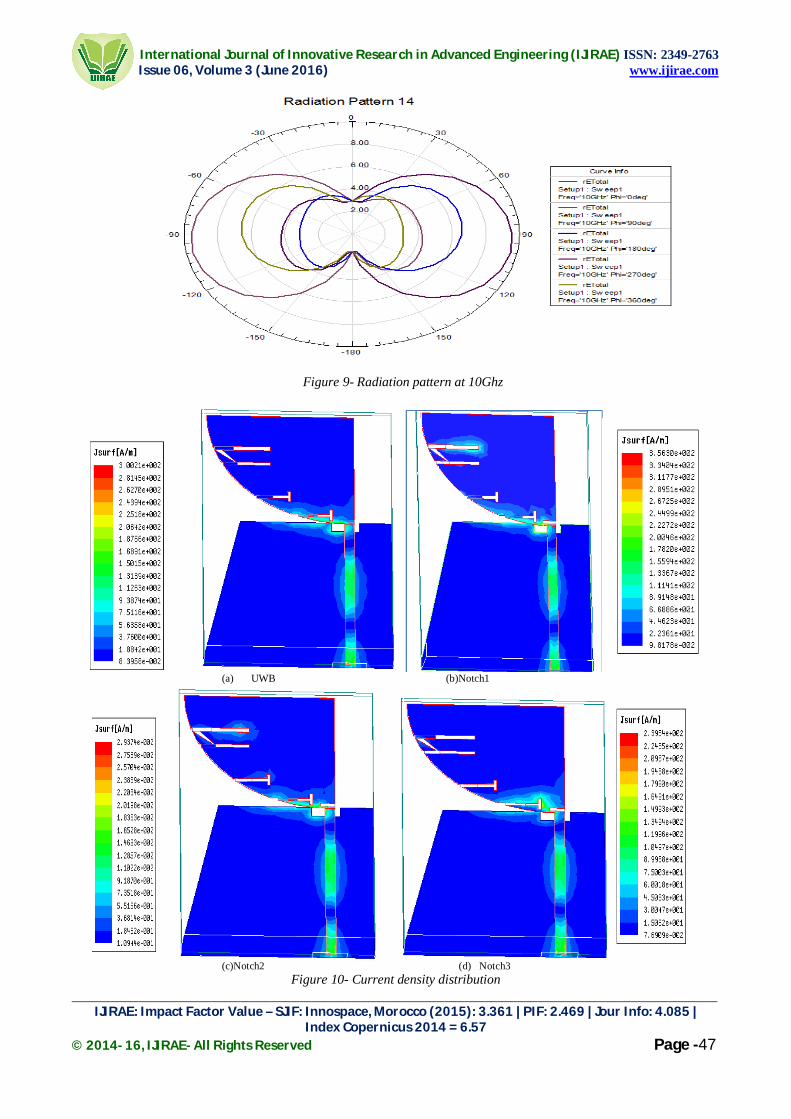
After that, a graph comparing the VSWR of above all four cases is drawn. From the above graph results, we can imply that the proposed antenna has the ability to avoid interferences from the three notched bands and can behave as a UWB antenna. Next, the radiation pattern of proposed triple band-notched UWB antenna is studied at a frequency 4Ghz,7GHz and 10Ghz and finally, surface current distribution are investigated and depicted for all the studied switch configurations .
Figure 6- VSWR vs Frequency for all four case
Figure 7- Radiation pattern at 7Ghz
Figure 8-Radiation pattern at 4Ghz
Frequency
VSWR
International Journal of Innovative Research in Advanced Engineering (IJIRAE) ISSN: 2349-2763 Issue 06, Volume 3 (June 2016) www.ijirae.com
_________________________________________________________________________________________________ IJIRAE: Impact Factor Value – SJIF: Innospace, Morocco (2015): 3.361 | PIF: 2.469 | Jour Info: 4.085 |
Index Copernicus 2014 = 6.57 © 2014- 16, IJIRAE- All Rights Reserved Page -47
Figure 9- Radiation pattern at 10Ghz
(a) UWB (b)Notch1
(c)Notch2 (d) Notch3
Figure 10- Current density distribution

International Journal of Innovative Research in Advanced Engineering (IJIRAE) ISSN: 2349-2763 Issue 06, Volume 3 (June 2016) www.ijirae.com
_________________________________________________________________________________________________ IJIRAE: Impact Factor Value – SJIF: Innospace, Morocco (2015): 3.361 | PIF: 2.469 | Jour Info: 4.085 |
Index Copernicus 2014 = 6.57 © 2014- 16, IJIRAE- All Rights Reserved Page -48
IV. CONCLUSIONS
A UWB antenna with quarter circle shaped patch has been designed and well investigated by the use of the HFSS. The notch bands are achieved by the slot technique. Four slots are etched on the patch to obtain the notched bands.. From the simulation of the design, we found that the proposed antenna can prevent the interferences from narrow band services.. The results prove that the analyzed antenna has a wide bandwidth. The notched bands have good values of return losses and VSWR. The designed antenna represents an effective device that enables the use of UWB technology with triple notch band functions.
. REFERENCES
[1] Anil K. Rathod,Multilayer Structured Rectangular Microstrip Antenna for ISM Band Applications,International Journal on Recent and Innovation Trends in Computing and Communication ISSN: 2321-8169 ,Volume: 3 Issue: 3,March 2015
[2] A. Petosa, “An Overview of tuning techniques for frequency-agile antennas,” IEEE Trans. Antennas Propag., vol. 54, no. 5, pp. 271–296,Oct. 2012.
[3] Arslan, H. and M. Sahin, UWB-based cognitive radio networks," Cognitive Wireless Com-munication Networks, E. Hossain and V. Bhargava, Ed., Springer, US, 2007
[4] A. Sheta and S. F. Mahmoud, “A widely tunable compact patchantenna,” IEEE Antennas Wireless Propag. Lett, vol. 7, pp. 40–42,2008
[5] B. Lakshmi priyanka, G.Krishnaveni, Dr.B.Manimegalai , Design and Simulation of Planar Monopole Antenna for UWB Applications, International Journal of Innovative Research in Science, Engineering and Technology, Volume 3, Special Issue 1, February 2014
[6] Kumar and Ray ,Broadband Microstrip Antennas,2nd edition ,2003 [7] Bybi P. Chacko, Gijo Augustin, and Tayeb A. Denidni, Senior Member, IEEE, Electronically Reconfigurable
Uniplanar AntennaWith Polarization Diversity for Cognitive Radio Applications , IEEE Antennas and Wireless Propagation Letters, VOL. 14, 2015
[8] Dipali Soren, Rowdra Ghatak, Rabindra K. Mishra, and Dipak R. Poddar, Dielectric Resonator Antennas: Designs and Advances, Progress In Electromagnetics Research B, Vol. 60, 195-213, 2014
[9] I. Lim and S. Lim, “Monopole-Like and boresight pattern reconfigurable antenna,” IEEE Trans. Antennas Propag, vol. 61, no. 12, pp.5854–5859, Dec. 2013.
[10] MiroslavJoler and JoškoKučan, Impact of the slot parameters on the three resonant frequencies of a rectangular microstrip antenna. Digital Object Identifier10.1109/MAP.2015.2453888, 1 September 2015
[11] Mohammad Jahanbakht, Abbas Ali LotfiNeyestanak, A Survey on Recent Approaches in the Design of Band Notching UWB Antennas, Journal of Electromagnetic Analysis and Applications, 2012, 4, 77-84
[12] Pendry, J. B., A. J. Holden, D. J. Robbins, and W. J. Stewart, \Magnetism from conductors and enhanced nonlinear phenomena," IEEE Trans. Microw. Theory Tech., Vol. 47, No. 11, 2075-2084, 1999.
[13] R.Garg, P.Bhartia, I. Bahl, Microstrip antenna design handbook ,Arthouse Inc., 2001 [14] Sivaranjani,PeesapatiPavani,SingavarapuVenkatesh,GaddamSivaNagaraju,DamarlaNagamadhavi circular
mictrostrip antenna design for ultrawideband [15] Yingsong LI, Wenxing LI, Tao JIANG,Implementation and Investigation of a Compact Circular Wide Slot UWB
Antenna with Dual Notched Band Characteristics using Stepped Impedance Resonators, RADIOENGINEERING, VOL. 21, NO. 1, APRIL 2012
[16] Heena Choudhary, Romika Choudhary,Ashish Vats,”Design and Analysis of Circular Patch MicroStrip UWB Antenna for Breast cancerDetection,” International Journal of Innovative Research in Science Engineering and Technology, Vol. 4, Issue 12, December 2015
[17] Heena Choudhary, Romika Choudhary,Ashish Vats,”Design of Frequency Reconfigurable Micro-Strip Patch Antenna for Wireless Applications,” International Journal of Innovative Research in Science Engineering and Technology, Vol. 4, Issue 12, December 2015
[18] Yuanyuan Kong, Yingsong Li, and Wenhua Yu,A Triple Band-notched UWB Antenna by Using an Arc-shaped Slotand a U-shaped Resonator Techniques, PIERS Proceedings, Prague, Czech Republic, July 6-9, 2015
[19] Xiao-lin Yang, Jian-cheng Lin, Gang Chen, and Fang-ling Kong, Frequency Reconfigurable Antenna for Wireless Communications Using GaAs FET Switch, IEEE ANTENNAS AND WIRELESS PROPAGATION LETTERS, VOL. 14, 2015


![A U-Shaped UWB Antenna with Band-Notched Performance · 2013. 12. 24. · 178 A U-Shaped UWB Antenna with Band-Notched Performance Units [mm] Conductor in back Conductor in front](https://img.pdfslide.us/doc/110x75/612da4881ecc51586942511a/a-u-shaped-uwb-antenna-with-band-notched-performance-2013-12-24-178-a-u-shaped.jpg)

![A Microstrip Patch Antenna with Defected Ground …coupling of the multi-band microstrip patch array is reduced. In [19], a defected ground structured compact plus shaped slot loaded](https://img.pdfslide.us/doc/110x75/5fd20002ebbc7a58c62a1838/a-microstrip-patch-antenna-with-defected-ground-coupling-of-the-multi-band-microstrip.jpg)