Embed Size (px)
Citation preview

© Semiconductor Components Industries, LLC, 2010
June, 2010 -- Rev. 31 Publication Order Number:
TND334/D
TND334/DRev. 3, JUN -- 2010
50 W Four--Output Internal PowerSupply for Set Top Box
Reference Design Documentation Package

http://onsemi.com2
Disclaimer:ONSemiconductor isproviding this referencedesigndocumentationpackage“ASIS”and the recipient assumesall risk associated with the use and/or commercialization of this design package. No licenses to ON Semiconductor’s or anythird party’s Intellectual Property is conveyed by the transfer of this documentation. This reference design documentationpackage is provided only to assist the customers in evaluation and feasibility assessment of the reference design. It is expectedthat users may make further refinements to meet specific performance goals.
TND334
http://onsemi.com3
TND334
50 W Four--Output InternalPower Supply for Set TopBox
Reference Design DocumentationPackage
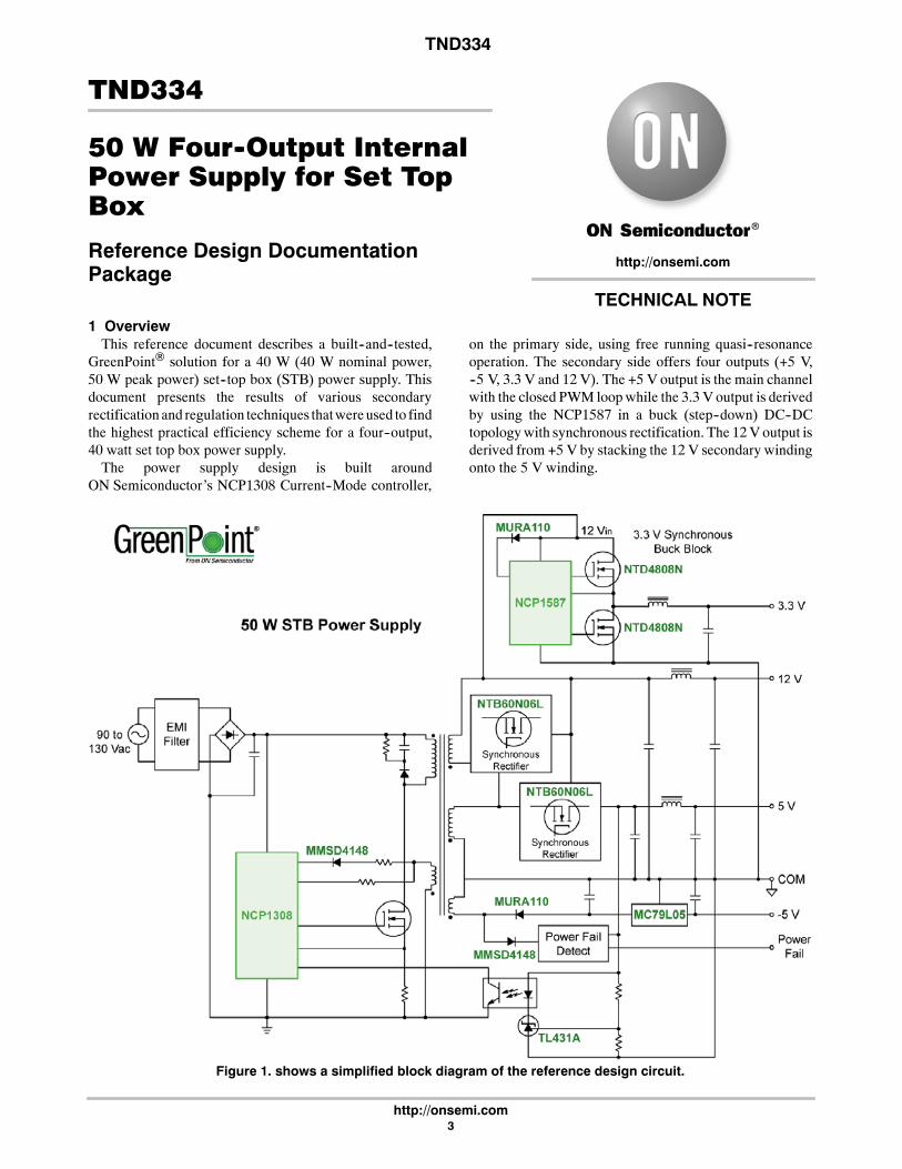
1 OverviewThis reference document describes a built--and--tested,
GreenPoint® solution for a 40 W (40 W nominal power,50 W peak power) set--top box (STB) power supply. Thisdocument presents the results of various secondaryrectification and regulation techniques thatwereused to findthe highest practical efficiency scheme for a four--output,40 watt set top box power supply.The power supply design is built around
ON Semiconductor’s NCP1308 Current--Mode controller,
on the primary side, using free running quasi--resonanceoperation. The secondary side offers four outputs (+5 V,--5 V, 3.3 V and 12 V). The +5 V output is the main channelwith the closed PWM loopwhile the 3.3 V output is derivedby using the NCP1587 in a buck (step--down) DC--DCtopologywith synchronous rectification. The 12V output isderived from +5 V by stacking the 12 V secondary windingonto the 5 V winding.
Figure 1. shows a simplified block diagram of the reference design circuit.
TECHNICAL NOTE
http://onsemi.com
TND334
http://onsemi.com4
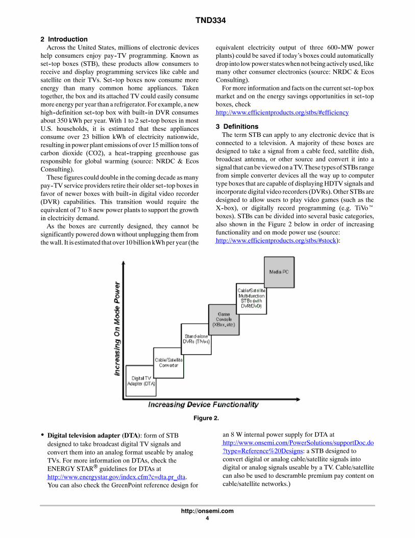
2 IntroductionAcross the United States, millions of electronic devices
help consumers enjoy pay--TV programming. Known asset--top boxes (STB), these products allow consumers toreceive and display programming services like cable andsatellite on their TVs. Set--top boxes now consume moreenergy than many common home appliances. Takentogether, the box and its attached TV could easily consumemore energy per year than a refrigerator. For example, a newhigh--definition set--top box with built--in DVR consumesabout 350 kWh per year. With 1 to 2 set--top boxes in mostU.S. households, it is estimated that these appliancesconsume over 23 billion kWh of electricity nationwide,resulting in power plant emissions of over 15million tons ofcarbon dioxide (CO2), a heat--trapping greenhouse gasresponsible for global warming (source: NRDC & EcosConsulting).These figures could double in the coming decade asmany
pay--TV service providers retire their older set--top boxes infavor of newer boxes with built--in digital video recorder(DVR) capabilities. This transition would require theequivalent of 7 to 8 new power plants to support the growthin electricity demand.As the boxes are currently designed, they cannot be
significantly powered downwithout unplugging them fromthewall. It is estimated that over 10billionkWhper year (the
equivalent electricity output of three 600--MW powerplants) could be saved if today’s boxes could automaticallydrop into lowpower stateswhennotbeingactivelyused, likemany other consumer electronics (source: NRDC & EcosConsulting).Formore information and facts on the current set--top box
market and on the energy savings opportunities in set--topboxes, checkhttp://www.efficientproducts.org/stbs/#efficiency
3 DefinitionsThe term STB can apply to any electronic device that is
connected to a television. A majority of these boxes aredesigned to take a signal from a cable feed, satellite dish,broadcast antenna, or other source and convert it into asignal that canbeviewedonaTV.These typesofSTBsrangefrom simple converter devices all the way up to computertype boxes that are capable of displayingHDTV signals andincorporate digital video recorders (DVRs). Other STBs aredesigned to allow users to play video games (such as theX--box), or digitally record programming (e.g. TiVotboxes). STBs can be divided into several basic categories,also shown in the Figure 2 below in order of increasingfunctionality and on mode power use (source:http://www.efficientproducts.org/stbs/#stock):
Figure 2.
• Digital television adapter (DTA): form of STBdesigned to take broadcast digital TV signals andconvert them into an analog format useable by analogTVs. For more information on DTAs, check theENERGY STAR® guidelines for DTAs athttp://www.energystar.gov/index.cfm?c=dta.pr_dta.You can also check the GreenPoint reference design for
an 8 W internal power supply for DTA athttp://www.onsemi.com/PowerSolutions/supportDoc.do?type=Reference%20Designs: a STB designed toconvert digital or analog cable/satellite signals intodigital or analog signals useable by a TV. Cable/satellitecan also be used to descramble premium pay content oncable/satellite networks.)

TND334
http://onsemi.com5
• Cable/satellite converter: a STB designed to convertdigital or analog cable/satellite signals into digital oranalog signals useable by a TV. Cable/satellite can alsobe used to descramble premium pay content oncable/satellite networks.
• Stand--alone Digital Video Recorders (DVRs): STBssuch as the TiVot that are designed to digitally recordTV content for instant playback
• Game Console: STB that allows the user to play videogames, browse web pages or otherwise interact withaudiovisual content displayed on a TV
• Cable/Satellite Multi--function STBs: a form ofcable/satellite converter that may contain a DVR, DVDrecorder, multiple cable/satellite tuners, etc. This typeof box is one focus of discussion on EfficientProducts.org
• Media PC: a personal computer designed to tunecable/satellite signals and that can display digital mediacontent on a TV screen without the need forintermediary audio or video adapters
The ENERGY STAR® specification for set--top boxes iscurrently under revision. On its web site, ENERGYSTAR®
provides the following definitions for the differentoperational modes and power states:• On/Active: An operational state in which the STB isactively delivering one or more of its principalfunctions and some or all of its applicable secondaryfunctions.
• Sleep: A state in which the STB has less powerconsumption, capability, and responsiveness than in theOn/Active state. The STB may enter a Sleep state fromthe On/Active state after:
a) the user pushes a power/standby button on theremote or on the unit; or
b) the STB auto power downs to a Sleep state. Theenergy consumption after auto power down toSleep and after a user--initiated power down toSleep may, or may not be, equivalent.
Note: EPA has decided to use the term “Sleep” rather than“Standby” to avoid confusionwith other EPA specificationsand international standards.
4 STB Power Supply SpecificationThe power supply specification called for four regulated
outputs with the following general requirements:
Input: Vin: 90 to 135 Vac, 55 to 65 Hz
Outputs
Vout Regulation Range Ripple (p/p) Inominal Imax Imin
3.3 Vdc 3.3 to 3.35 V 40 mV 3.37 A 3.9 A 1.85 A
5.0 Vdc 4.9 to 5.25 V 40 mV 1.52 A 2.2 A 0.70 A
12 Vdc 11.4 to 12.6 V 120 mV 0.78 A 1.2 A 0.24 A
--5.0 Vdc --4.85 to --5.25 V 20 mV 38 mV 58 mA 18 mA
Total Power Output = 28.27 W 38.56 W 12.57 W
Over--current protection on all outputs with self recovery
Efficiency: > 80%
Five different secondary output configurations were implemented using the same primary “front end” quasi--resonant (QR)flyback converter stage, and the efficiency and performance characteristics of each were measured.
TND334
http://onsemi.com6
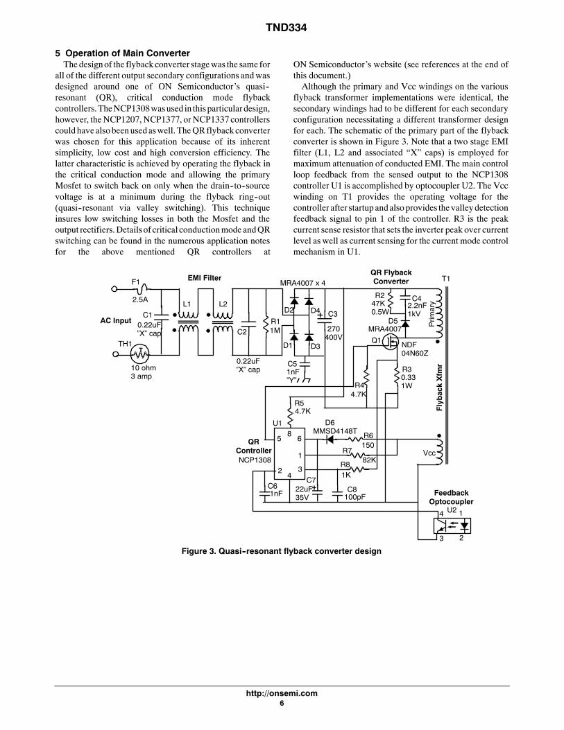
5 Operation of Main ConverterThedesignof the flyback converter stagewas the same for
all of the different output secondary configurations andwasdesigned around one of ON Semiconductor’s quasi--resonant (QR), critical conduction mode flybackcontrollers.TheNCP1308wasused in thisparticulardesign,however, theNCP1207, NCP1377, or NCP1337 controllerscouldhave alsobeenusedaswell. TheQRflybackconverterwas chosen for this application because of its inherentsimplicity, low cost and high conversion efficiency. Thelatter characteristic is achieved by operating the flyback inthe critical conduction mode and allowing the primaryMosfet to switch back on only when the drain--to--sourcevoltage is at a minimum during the flyback ring--out(quasi--resonant via valley switching). This techniqueinsures low switching losses in both the Mosfet and theoutput rectifiers.Detailsof critical conductionmodeandQRswitching can be found in the numerous application notesfor the above mentioned QR controllers at
ON Semiconductor’s website (see references at the end ofthis document.)Although the primary and Vcc windings on the various
flyback transformer implementations were identical, thesecondary windings had to be different for each secondaryconfiguration necessitating a different transformer designfor each. The schematic of the primary part of the flybackconverter is shown in Figure 3. Note that a two stage EMIfilter (L1, L2 and associated “X” caps) is employed formaximum attenuation of conducted EMI. The main controlloop feedback from the sensed output to the NCP1308controller U1 is accomplished by optocoupler U2. The Vccwinding on T1 provides the operating voltage for thecontroller after startupandalsoprovides thevalleydetectionfeedback signal to pin 1 of the controller. R3 is the peakcurrent sense resistor that sets the inverter peak over currentlevel as well as current sensing for the current mode controlmechanism in U1.
T
AC Input
1
2 34
5 68
1
2
4
3
T1
10 ohm3 amp
2.5A
0.22uF”X” cap
0.22uF”X” cap
EMI Filter
1M
MRA4007 x 4
MRA4007
NDF04N60Z
47K0.5W
2.2nF1kV
4.7K
1nF”Y” 0.33
1W
MMSD4148T
150
82K
1K
100pF22uF35V1nF
270400V
4.7K
QR FlybackConverterF1
TH1
L1 L2
U2
C1
C2R1
D1
D2
D3
D4D5
R2 C4
Q1
C5
C3
R3
R4
R5
D6
R7
R6
R8
C8C7
C6
U1
NCP1308
FeedbackOptocoupler
QRController Vcc
Prim
ary
FlybackXfm
r
Figure 3. Quasi--resonant flyback converter design
TND334
http://onsemi.com7
6 Secondary Circuit ApproachesFive different secondary circuit designs were tested. The
circuitry included the use of Mosfet synchronous rectifiersfor themain flybackwinding and synchronousMosfet buckconverters for low voltage post regulators in severaldifferent configurations which are described below.
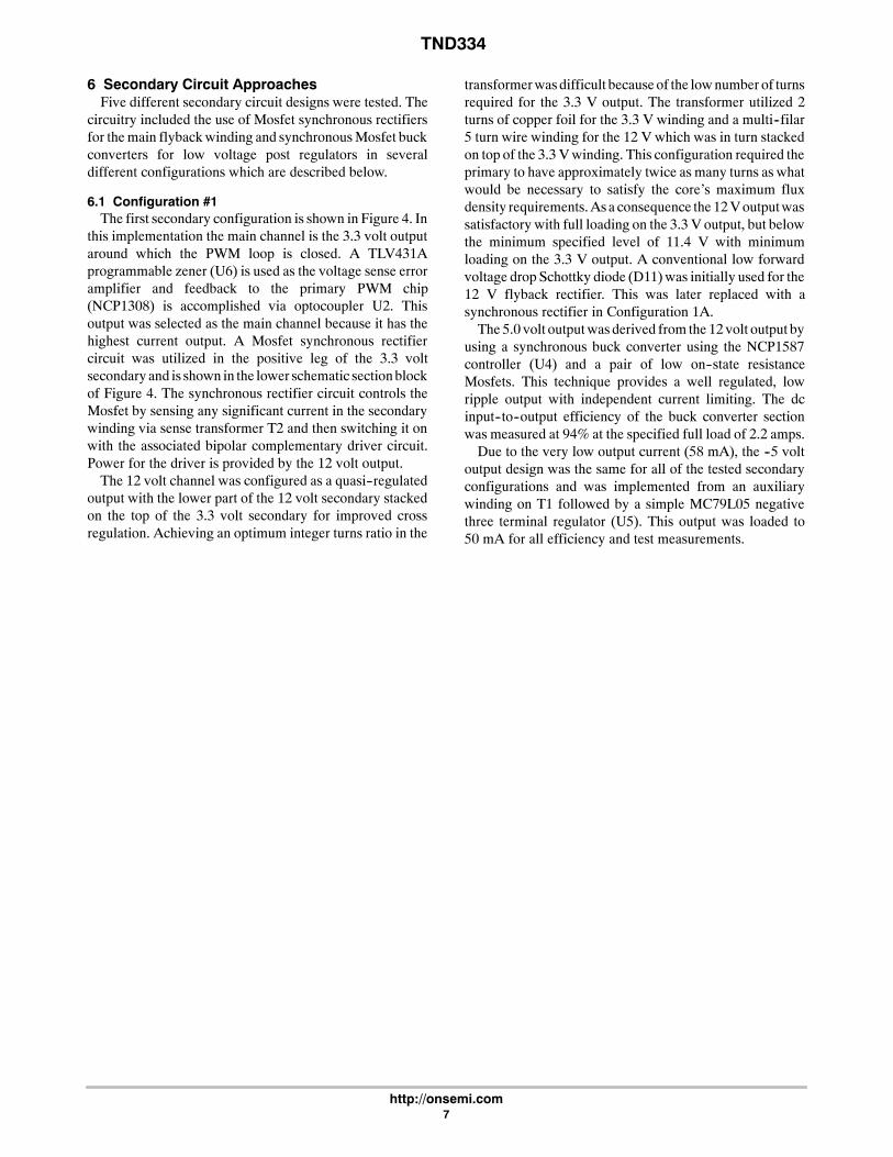
6.1 Configuration #1The first secondary configuration is shown in Figure 4. In
this implementation the main channel is the 3.3 volt outputaround which the PWM loop is closed. A TLV431Aprogrammable zener (U6) is used as the voltage sense erroramplifier and feedback to the primary PWM chip(NCP1308) is accomplished via optocoupler U2. Thisoutput was selected as the main channel because it has thehighest current output. A Mosfet synchronous rectifiercircuit was utilized in the positive leg of the 3.3 voltsecondary and is shown in the lower schematic sectionblockof Figure 4. The synchronous rectifier circuit controls theMosfet by sensing any significant current in the secondarywinding via sense transformer T2 and then switching it onwith the associated bipolar complementary driver circuit.Power for the driver is provided by the 12 volt output.The 12 volt channel was configured as a quasi--regulated
output with the lower part of the 12 volt secondary stackedon the top of the 3.3 volt secondary for improved crossregulation. Achieving an optimum integer turns ratio in the
transformerwasdifficult because of the lownumber of turnsrequired for the 3.3 V output. The transformer utilized 2turns of copper foil for the 3.3 V winding and a multi--filar5 turn wire winding for the 12 V which was in turn stackedon top of the 3.3 Vwinding. This configuration required theprimary to have approximately twice as many turns as whatwould be necessary to satisfy the core’s maximum fluxdensity requirements.Asa consequence the 12Voutputwassatisfactory with full loading on the 3.3 V output, but belowthe minimum specified level of 11.4 V with minimumloading on the 3.3 V output. A conventional low forwardvoltage drop Schottky diode (D11)was initially used for the12 V flyback rectifier. This was later replaced with asynchronous rectifier in Configuration 1A.The 5.0 volt outputwas derived from the 12volt output by
using a synchronous buck converter using the NCP1587controller (U4) and a pair of low on--state resistanceMosfets. This technique provides a well regulated, lowripple output with independent current limiting. The dcinput--to--output efficiency of the buck converter sectionwas measured at 94% at the specified full load of 2.2 amps.Due to the very low output current (58 mA), the --5 volt
output design was the same for all of the tested secondaryconfigurations and was implemented from an auxiliarywinding on T1 followed by a simple MC79L05 negativethree terminal regulator (U5). This output was loaded to50 mA for all efficiency and test measurements.
TND334
http://onsemi.com8
MURA110
NTD--4808N
12V
3.3V
--5V
Com
1
2
4
3
--5Vreg
1 2
3 4
5
6
78
5V
MC79L05
MBR1045
10K 0.1
0.1
0.1
TLV431A
5.1K
3.3K
39
4.7K
(4.7K) 0.1
12006.3V
4.7uH
4.7uH680, 16V x 2
68016V
2.2K
27025V 270
25V
10uH
0.1
12006.3V
NTD4808N
NCP1587
1nF
10
MURA1100.1
0.1
100pF
50nF
Synchronous Buck (5V)
3.3VoutError Amp
1200uF6.3V x 3
SynchronousRectifierBlock
Vcc
A B
27K5.1K
10K
D11
C13
R20 C12
C14
R22
R21
C11Q4
Q5L3
L5
L4
C17C16
C15
R23
D10
C18 C19 C20 R24C21
C27 C28C24,25,26
C29 C30C31U5
R29
D12
U2
U6
R30
R31R32
R33
R34
C32
U4
T1
MMSD4148T
1nF
1K
100
MMBT2222A
MMBT2222A
20K1K
MMBT2907A
1T
50T
Vcc
A B
3.3 Vout Synchronous Rectifier Block
NTB60N06LT
0.1T2C23
Q6
Q7
Q8
Q9
D12
R27R26
R28
R25
C22
Figure 4. Secondary Configuration #1
6.2 Configuration #1AIn this configuration the Schottky rectifier for the 12 volt
channel (D11) was replaced with a synchronous rectifierexactly like the one for the 3.3 V output and the efficiencywas measured again. This configuration did improve the
overall efficiency and placed the 3.3 V to 12 Vcross--regulation just within specification limits due to theelimination of the Schottky diode forward drop thatsubtracts from the effective output voltage.
TND334
http://onsemi.com9
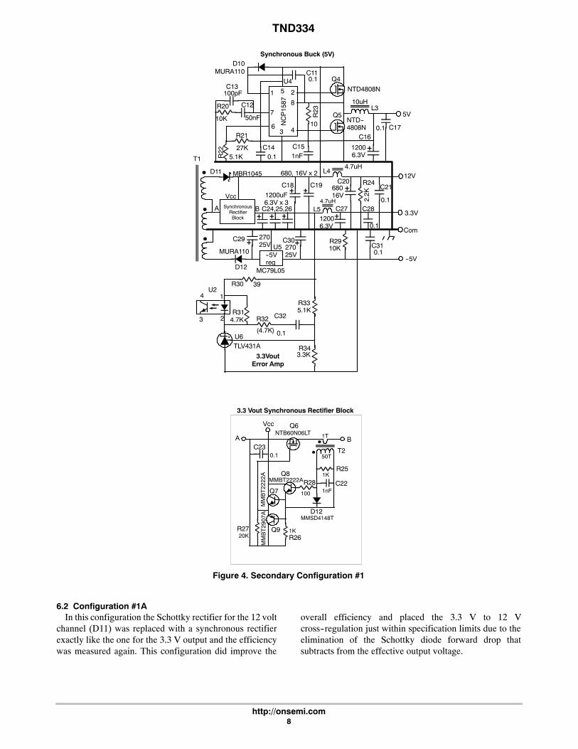
6.3 Configuration #2In the second configuration, the main channel was the 12
volt output with the PWM loop closed around it. A TL431Aerror amp and optocoupler combination was used in asimilar PWM feedback scheme as in Configuration 1. Asmentioned previously, the --5 V output was the same as inConfiguration 1. A current sensed synchronous rectifiercircuitwasalsoused for this output, however, the circuitwasimplemented in the lower leg of the secondary winding dueto the fact that the operating Vcc for the sync circuit had tocome from the 12 volt output also. The schematic ofConfiguration 2 is shown in Figure 5 and the synchronousrectifier schematic block is shown to the lower left of themain schematic.Both the 5 volt and 3.3 volt channels were derived from
the 12 volt output with NCP1587 buck converters identical
to the 5.0 volt buck in Configuration 1. The detailedschematic of the buck converter block is shown at the lowerright of Figure 5. The measured dc input--to--outputefficiency of the 3.3 volt converter section was 92% with aload of 3.9 amps.The principle advantage of this particular configuration
was the simplicity of the flyback transformer design.Because of the higher voltage of the 12 V secondary, it waseasy to configure the turns ratio of the windings for lowleakage inductance andminimalwinding layers. In additionthe lack of quasi--regulated (slave) outputs eliminates allcross--regulation issues and all outputs are tightly regulatedwith low ripple and independently current limited.
C25
12V
3.3V
--5V
Com
1
2
4
3
--5Vreg
5V
MURA110
MC79L05
10K 0.1
0.1
TL431A3.3K
470
1K
10K 0.1
4.7uH680uF,16V x 2
68016V
27025V 270
25V
12V Error Amp
SynchronousRectifierBlock
Vcc
A B
L4
C18 C19C20
R24
C21
C27
U5
R29
D10
U2
U6
R30
R31R32
R33
3.3V SynchronousBuck Block
5V SynchronousBuck Block
Com
Com
Vout
Vout12Vin
12Vin
13K
C24C26
T1
12 Vout Synchronous Rectifier Block
MMBT2222A
MMSD4148T
1nF
1K
100
MMBT2222A
20K1K
MMBT2907A
1T
50T
Vcc
A BNTB60N06LT
0.1T2 C23
Q6
Q7
Q8
Q9
D12
R27R26
R28
R25
C22
Synchronous Buck Block
NTD--4808N
1 2
3 4
5
6
78 10uH
0.1
12006.3V
NTD4808N
NCP1587
1nF
10
MURA110
0.1
0.1
100pF
50nF
Vset5.1K
(10K)
D11
C13
R20 C12
C14
R22
R21
C11Q4
Q5L3
C17C16
C15
R23
U4
12Vin
Vout
Com
Figure 5. Secondary Configuration #2
TND334
http://onsemi.com10
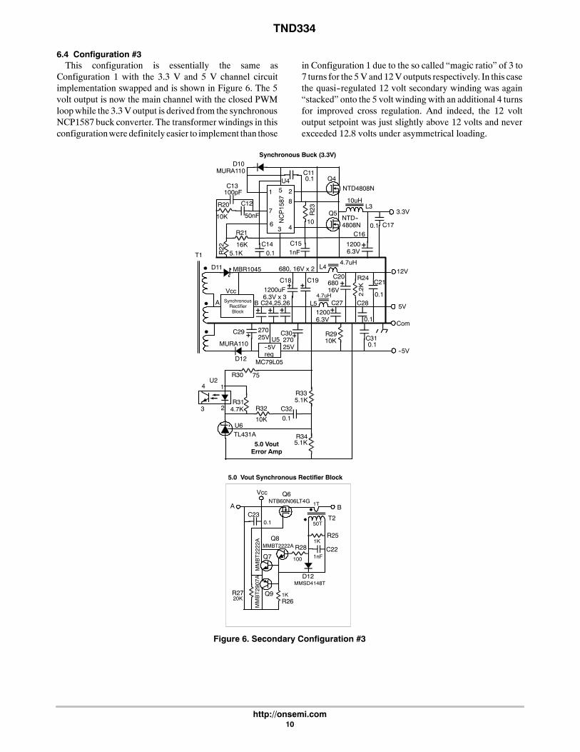
6.4 Configuration #3This configuration is essentially the same as
Configuration 1 with the 3.3 V and 5 V channel circuitimplementation swapped and is shown in Figure 6. The 5volt output is now the main channel with the closed PWMloopwhile the 3.3V output is derived from the synchronousNCP1587 buck converter. The transformer windings in thisconfigurationweredefinitely easier to implement than those
in Configuration 1 due to the so called “magic ratio” of 3 to7 turns for the 5V and 12Voutputs respectively. In this casethe quasi--regulated 12 volt secondary winding was again“stacked” onto the 5 volt winding with an additional 4 turnsfor improved cross regulation. And indeed, the 12 voltoutput setpoint was just slightly above 12 volts and neverexceeded 12.8 volts under asymmetrical loading.
MURA110
NTD--4808N
12V
3.3V
--5V
Com
1
2
4
3
--5Vreg
1 2
3 4
5
6
78
5V
MC79L05
MBR1045
10K 0.1
0.1
0.1
TL431A
5.1K
5.1K
75
4.7K
10K 0.1
12006.3V
4.7uH
4.7uH680, 16V x 2
68016V
2.2K
27025V 270
25V
10uH
0.1
12006.3V
NTD4808N
NCP1587
1nF
10
MURA1100.1
0.1
100pF
50nF
Synchronous Buck (3.3V)
5.0 VoutError Amp
1200uF6.3V x 3
SynchronousRectifierBlock
Vcc
A B
16K5.1K
10K
D11
C13
R20 C12
C14
R22
R21
C11Q4
Q5L3
L5
L4
C17C16
C15
R23
D10
C18 C19 C20 R24C21
C27 C28C24,25,26
C29 C30C31U5
R29
D12
U2
U6
R30
R31R32
R33
R34
C32
U4
T1
MMBT2222A
MMSD4148T
1nF
1K
100
MMBT2222A
20K1K
MMBT2907A
1T
50T
Vcc
A B
5.0 Vout Synchronous Rectifier Block
NTB60N06LT4G
0.1T2C23
Q6
Q7
Q8
Q9
D12
R27R26
R28
R25
C22
Figure 6. Secondary Configuration #3
TND334
http://onsemi.com11
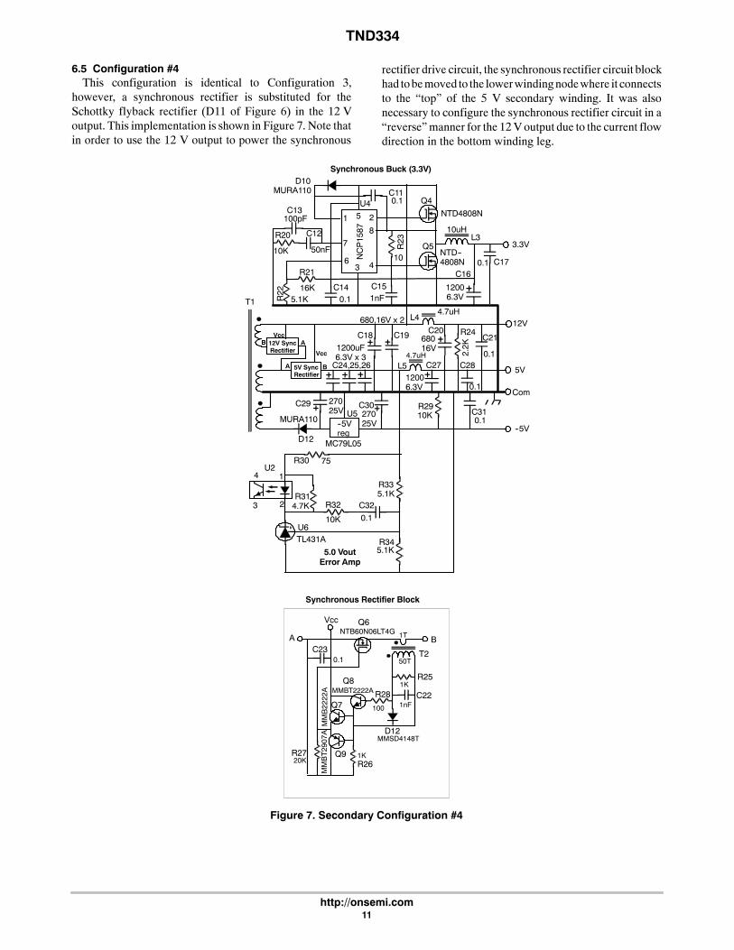
6.5 Configuration #4This configuration is identical to Configuration 3,
however, a synchronous rectifier is substituted for theSchottky flyback rectifier (D11 of Figure 6) in the 12 Voutput. This implementation is shown in Figure 7. Note thatin order to use the 12 V output to power the synchronous
rectifier drive circuit, the synchronous rectifier circuit blockhad tobemoved to the lowerwindingnodewhere it connectsto the “top” of the 5 V secondary winding. It was alsonecessary to configure the synchronous rectifier circuit in a“reverse”manner for the 12Voutput due to the current flowdirection in the bottom winding leg.
12V SyncRectifier
5V SyncRectifier
MURA110
NTD--4808N
12V
3.3V
--5V
Com
1
2
4
3
--5Vreg
1 2
3 4
5
6
78
5V
MC79L05
10K 0.1
0.1
0.1
TL431A
5.1K
5.1K
75
4.7K
10K 0.1
12006.3V
4.7uH
4.7uH680,16V x 2
68016V
2.2K
27025V 270
25V
10uH
0.1
12006.3V
NTD4808N
NCP1587
1nF
10
MURA1100.1
0.1
100pF
50nF
Synchronous Buck (3.3V)
5.0 VoutError Amp
1200uF6.3V x 3
Vcc
Vcc
A
B
B
A
16K5.1K
10K
C13
R20 C12
C14R22
R21
C11Q4
Q5L3
L5
L4
C17C16
C15
R23
D10
C18 C19 C20 R24C21
C27 C28C24,25,26
C29 C30C31U5
R29
D12
U2
U6
R30
R31R32
R33
R34
C32
U4
T1
Synchronous Rectifier Block
MMBT2222A
MMSD4148T
1nF
1K
100
MMB2222A
20K1K
MMBT2907A
1T
50T
Vcc
A BNTB60N06LT4G
0.1T2C23
Q6
Q7
Q8
Q9
D12
R27R26
R28
R25
C22
Figure 7. Secondary Configuration #4

TND334
http://onsemi.com12
7 Test Results7.1 Active Mode EfficiencyThe throughput efficiency of each of the configurations
was measured using fixed precision resistive loads and aVoltech PM1000 line analyzer. The power supply inputvoltage was 117 Vac and the loads were configured for thefollowing currents at the nominal output voltage:
Original Load Profile
Vout Nominal Output Current Watts
3.3 Vdc 3.4 A 11.22
5.0 Vdc 2.0 A 10.0
12.0 Vdc 1.2 A 14.4
--5.0 Vdc 50 mA 0.25
Total Output Power = 35.87 W
The measured efficiency for each configuration is asfollows:
Configuration Efficiency
Configuration #1: 77.6%
Configuration #1A: 78.5%
Configuration #2: 79.5%
Configuration #3: 80.2%
Configuration #4: 81%
Since Configuration #4 produced the highest efficiencyfor the specified loading, a new pc board layout wasimplemented and optimized for this configuration. Fiveadditional loading profiles were tested to determine theeffect of the load distribution on efficiency. Tests wereperformed with an input of 120 Vac and a total load of40 watts. The --5 volt output was loaded to 50 mA in eachcase. The results are shown in Table 1.
Table 1. Efficiency vs. Output Loading Profile
Different Load Profile of Outputsfor Configuration 4 Efficiency
Wattage per Channel (Total = 40 W)
3.3 V 5.0 V 12 V
Original load profile 81% 11.22 W 10 W 14.4 W
1 78.20% 15 W 15 W 10 W
2 81.20% 11 W 10 W 18 W
3 81.80% 8 W 15 W 18 W
4 82.70% 8 W 10 W 24 W
5 83.60% 5.4 W 10 W 24 W
7.2 Comments and ConclusionsTheefficiency results showthat for theoriginal tested load
profile, which is just slightly less than the maximumspecified loads but greater than the nominal load, only twoconfigurations produced an efficiency of 80% or better.Also, the fact that the efficiency spread is concentratedaround an average of about 79% indicates that it is probablydifficult to obtain greater efficiencies (with the specifiedload distribution) without some serious circuit designcompromises. Some other interesting observations are asfollows:
1. Having to resort to multiple winding techniques(foil and wire), and greater than optimal primaryturns to accommodate proper turns ratios as inConfiguration 1, can result in detrimental leakageinductance effects (as well as more expensivemagnetics). Adding the synchronous rectifier ofConfiguration #1A did improve the efficiency andcross--regulation but was not sufficient to achieve80%.
2. Using synchronous buck converters to produce thetwo high current, low voltage outputs (5 V and3.3 V) from the 12 V output (Configuration #2)was the “cleanest” design from the standpoint ofthe transformer construction and cross--regulation
issues, but was still unable to attain 80% efficiency.Additional testing of Configuration #2 wasperformed in which the 12 V output was loaded tothe full 36 watts (3 A load) and the two dc--dcsynchronous bucks for 3.3 V and 5 V and the--5 Vout were disconnected. The efficiency of thissingle output configuration was 85.6%.The product of this efficiency, which is essentiallythe efficiency of the flyback conversion stage, timesthe average efficiency of the two dc--dc synchronousbucks (92%, see Configuration #2 in section 6.2)mentioned in the Configuration #2 descriptionabove, yields a total throughput efficiency of 79.5%(86.5% * 92% = 79.5%) which is exactly what themeasured efficiency of Configuration #2 was (seetest results in section 7.1).
3. Using the ideal 3 to 7 turns ratio for the 5 V and12 V transformer windings in Configuration #3and #4, closing the PWM loop around the 5 Voutput, and deriving the 3.3 V via a synchronousbuck appears to be the best compromise forhighest efficiency. Also replacing the 12 VoutSchottky rectifier with a synchronous rectifier
TND334
http://onsemi.com13
increased the efficiency almost an extra point forConfiguration #4.
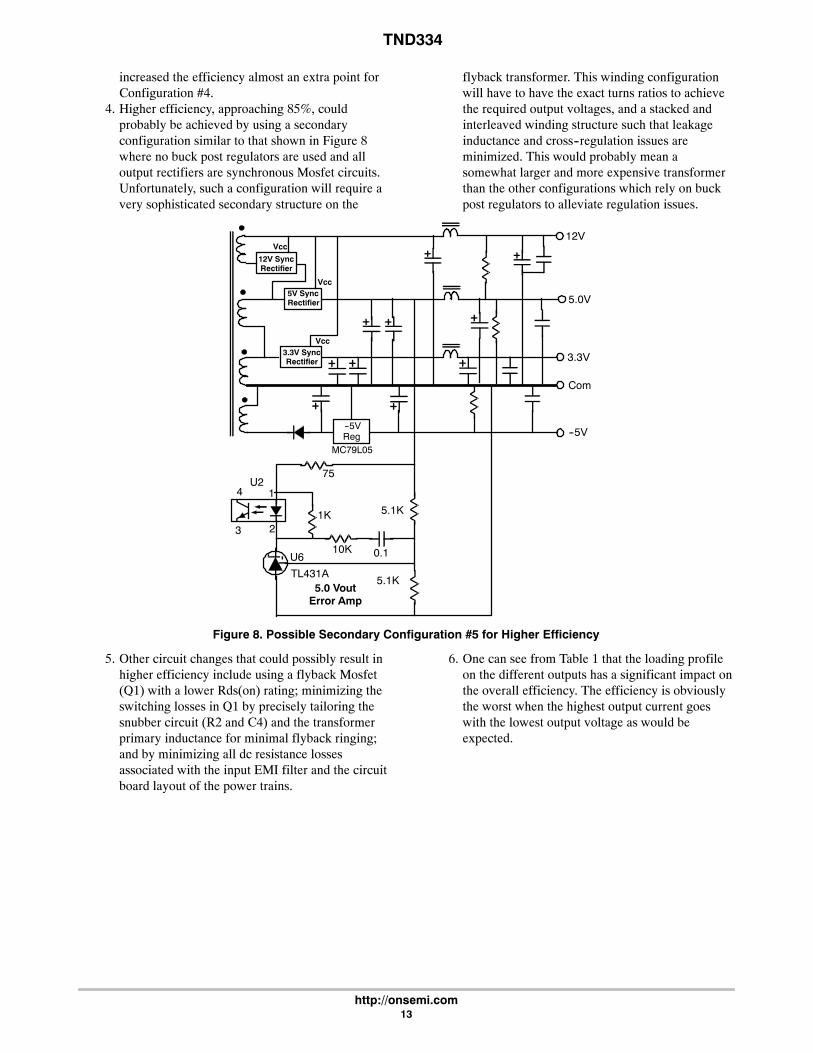
4. Higher efficiency, approaching 85%, couldprobably be achieved by using a secondaryconfiguration similar to that shown in Figure 8where no buck post regulators are used and alloutput rectifiers are synchronous Mosfet circuits.Unfortunately, such a configuration will require avery sophisticated secondary structure on the
flyback transformer. This winding configurationwill have to have the exact turns ratios to achievethe required output voltages, and a stacked andinterleaved winding structure such that leakageinductance and cross--regulation issues areminimized. This would probably mean asomewhat larger and more expensive transformerthan the other configurations which rely on buckpost regulators to alleviate regulation issues.
5V SyncRectifier
--5V
Com
1
2
4
3
--5VReg
MC79L05
TL431A
5.1K
5.1K
75
1K
10K 0.1
5.0 VoutError Amp
Vcc
Vcc
Vcc
U2
U6
12V SyncRectifier
3.3V SyncRectifier 3.3V
5.0V
12V
Figure 8. Possible Secondary Configuration #5 for Higher Efficiency
5. Other circuit changes that could possibly result inhigher efficiency include using a flyback Mosfet(Q1) with a lower Rds(on) rating; minimizing theswitching losses in Q1 by precisely tailoring thesnubber circuit (R2 and C4) and the transformerprimary inductance for minimal flyback ringing;and by minimizing all dc resistance lossesassociated with the input EMI filter and the circuitboard layout of the power trains.
6. One can see from Table 1 that the loading profileon the different outputs has a significant impact onthe overall efficiency. The efficiency is obviouslythe worst when the highest output current goeswith the lowest output voltage as would beexpected.
TND334
http://onsemi.com14
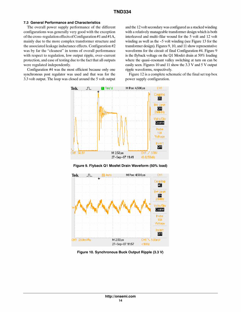
7.3 General Performance and CharacteristicsThe overall power supply performance of the different
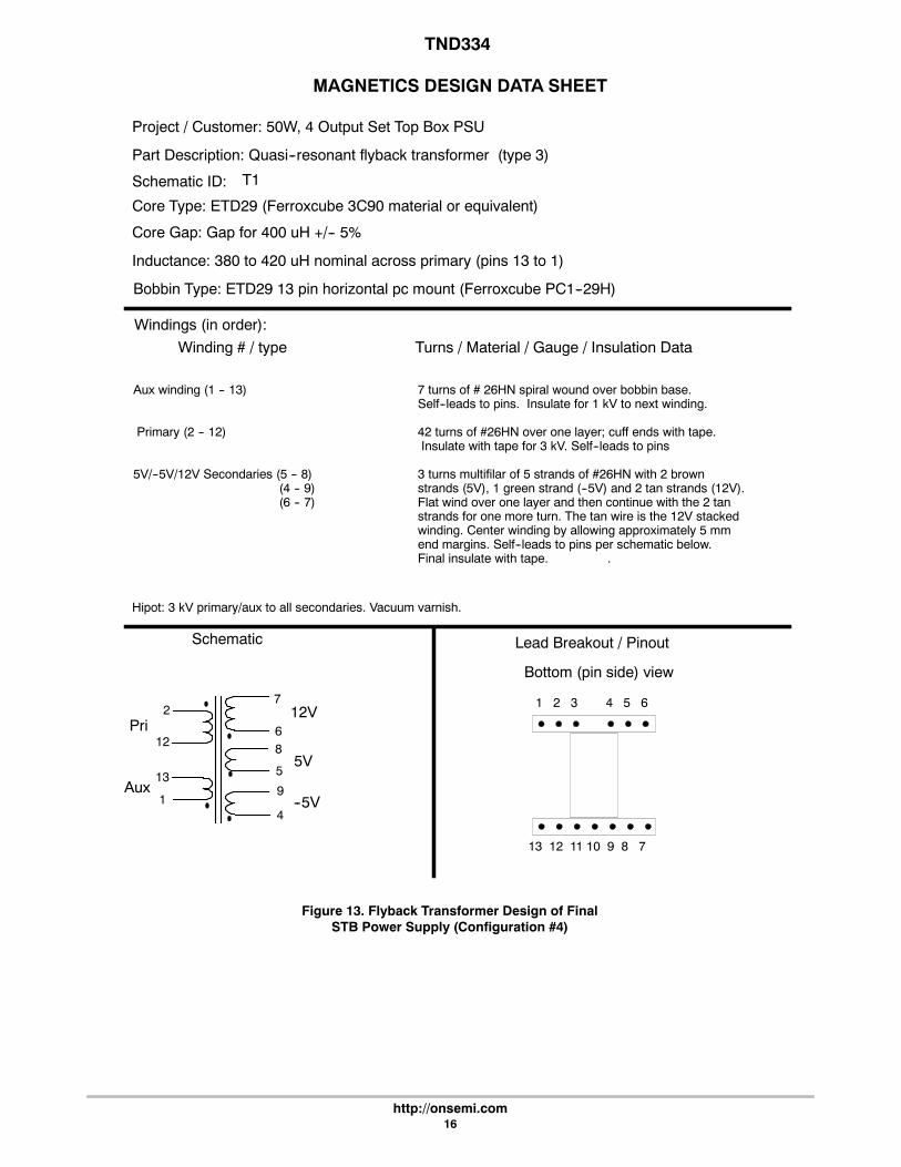
configurations was generally very good with the exceptionof the cross--regulation effects ofConfiguration#1 and#1A,mainly due to the more complex transformer structure andthe associated leakage inductance effects. Configuration #2was by far the “cleanest” in terms of overall performancewith respect to regulation, low output ripple, over--currentprotection, and ease of testing due to the fact that all outputswere regulated independently.Configuration #4 was the most efficient because only one
synchronous post regulator was used and that was for the3.3 volt output. The loop was closed around the 5 volt output
and the 12 volt secondarywas configured as a stackedwindingwith a relatively manageable transformer designwhich is bothinterleaved and multi--filar wound for the 5 volt and 12 voltwinding as well as the --5 volt winding (see Figure 13 for thetransformer design). Figures 9, 10, and 11 show representativewaveforms for the circuit of final Configuration #4. Figure 9is the flyback voltage on the Q1 Mosfet drain at 50% loadingwhere the quasi--resonant valley switching at turn on can beeasily seen. Figures 10 and 11 show the 3.3 V and 5 V outputripple waveforms, respectively.Figure 12 is a complete schematic of the final set top box
power supply configuration.
Figure 9. Flyback Q1 Mosfet Drain Waveform (50% load)
Figure 10. Synchronous Buck Output Ripple (3.3 V)
TND334
http://onsemi.com15
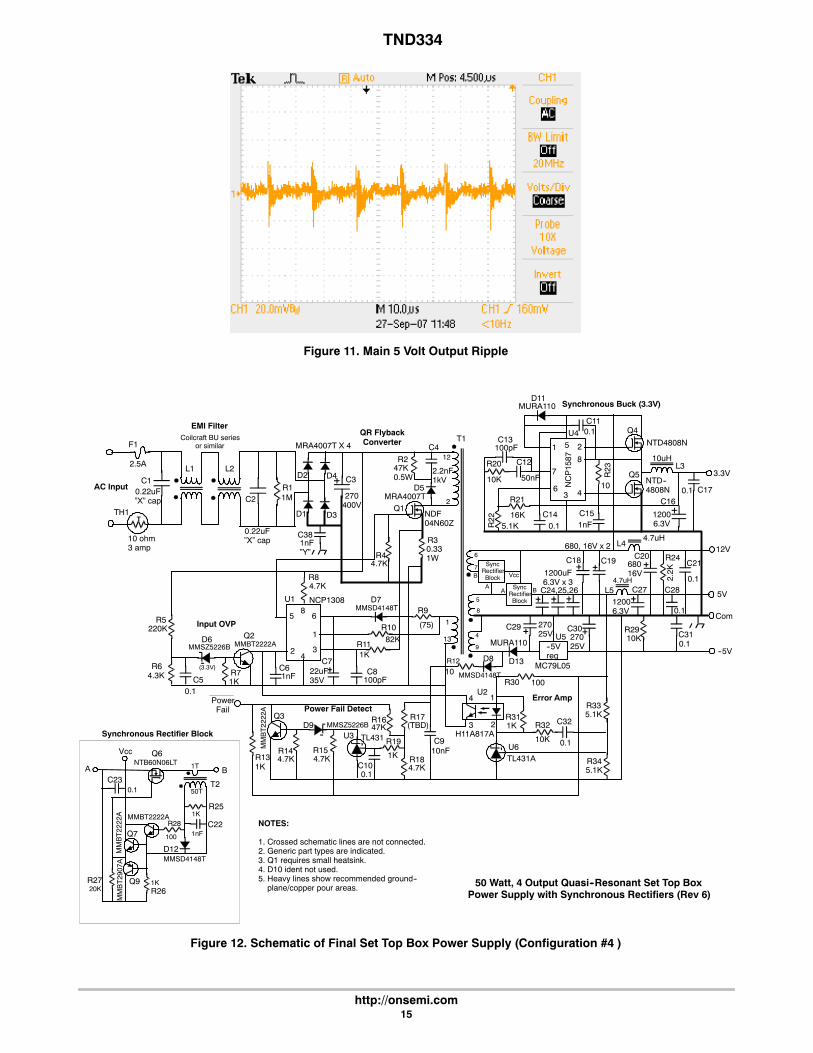
Figure 11. Main 5 Volt Output Ripple
NTD--4808N
T
AC Input
1
2 34
5 68
12V
3.3V
--5V
Com
PowerFail
1
2
4
3
T1
--5Vreg
1 2
3 4
5
6
78
5V
50 Watt, 4 Output Quasi--Resonant Set Top BoxPower Supply with Synchronous Rectifiers (Rev 6)
10 ohm3 amp
2.5A
0.22uF”X” cap
0.22uF”X” cap
EMI Filter
1M
MRA4007T X 4
MRA4007T
NDF04N60Z
47K0.5W
2.2nF1kV
4.7K
1nF”Y” 0.33
1W
(75)
82K
1K
100pF22uF35V1nF
270400V
4.7K
TL431
MMSZ5226B
MMSZ5226B
1K4.7K 4.7K
0.14.7K
1K
47K (TBD)
10nF
10 MMSD4148T
MURA110
MC79L05
10K0.1
0.1
0.1
TL431A
5.1K
5.1K
100
1K
10K 0.1H11A817A
12006.3V
4.7uH
4.7uH680, 16V x 2
68016V
2.2K
27025V 270
25V
10uH
0.1
12006.3V
NTD4808N
NCP1587
1nF
10
MURA110
0.1
0.1
100pF
50nF
Synchronous Buck (3.3V)
Error AmpPower Fail Detect
QR FlybackConverter
1200uF6.3V x 3
Vcc
AA
B
B
16K5.1K
MMBT2222A
MMBT2222A
1K0.1
220K Input OVP
4.3K(3.3V)
Coilcraft BU seriesor similar
10K
F1
TH1
L1 L2
1nF
1K
100
20K1K
1T
50T
Vcc
A B
Synchronous Rectifier Block
NTB60N06LT
0.1T2C23
Q6
Q7
Q9
D12
R27R26
R28
R25
C22
D11
C13
R20 C12
C14
R22
R21
C11Q4
Q5L3
L5
L4
C17C16
C15
R23
C18 C19 C20 R24C21
C27 C28C24,25,26
C29 C30C31U5
R29
D13D8R12
U2
U6
R30
R31R32
R33
R34
C32
C1
C2R1
D1
D2
D3
D4D5
R2C4
Q1
Q2
C38
C3
R3
R4
R8
R5
R6
D6
D7
D9
R10
R9
R11
C8C7
C6C5
R7
U1 NCP1308
R13R14 R15
U3
R16 R17
R18
R19 C9
C10
Q3
U4
NOTES:
1. Crossed schematic lines are not connected.2. Generic part types are indicated.3. Q1 requires small heatsink.4. D10 ident not used.5. Heavy lines show recommended ground--plane/copper pour areas.
SyncRectifierBlock
SyncRectifierBlock
2
12
13
1
7
6
8
5
9
4
MMSD4148T
MMBT2222A
MMBT2222A
MMBT2907A MMSD4148T
Figure 12. Schematic of Final Set Top Box Power Supply (Configuration #4 )
TND334
http://onsemi.com16
MAGNETICS DESIGN DATA SHEET
Part Description: Quasi--resonant flyback transformer (type 3)
Project / Customer: 50W, 4 Output Set Top Box PSU
Schematic ID:
Core Type: ETD29 (Ferroxcube 3C90 material or equivalent)
Core Gap: Gap for 400 uH +/-- 5%
Inductance: 380 to 420 uH nominal across primary (pins 13 to 1)
Bobbin Type: ETD29 13 pin horizontal pc mount (Ferroxcube PC1--29H)
Windings (in order):Winding # / type Turns / Material / Gauge / Insulation Data
Hipot: 3 kV primary/aux to all secondaries. Vacuum varnish.
Schematic Lead Breakout / Pinout
T1
Aux winding (1 -- 13) 7 turns of # 26HN spiral wound over bobbin base.Self--leads to pins. Insulate for 1 kV to next winding.
Primary (2 -- 12) 42 turns of #26HN over one layer; cuff ends with tape.Insulate with tape for 3 kV. Self--leads to pins
5V/--5V/12V Secondaries (5 -- 8) 3 turns multifilar of 5 strands of #26HN with 2 brown(4 -- 9) strands (5V), 1 green strand (--5V) and 2 tan strands (12V).(6 -- 7) Flat wind over one layer and then continue with the 2 tan
strands for one more turn. The tan wire is the 12V stackedwinding. Center winding by allowing approximately 5 mmend margins. Self--leads to pins per schematic below.Final insulate with tape. .
Bottom (pin side) view
Pri
Aux13
1
1 2 3 4 5 6
13 12 11 10 9 8 7
2
12
7
4
9
6
5V
12V
--5V
5
8
Figure 13. Flyback Transformer Design of FinalSTB Power Supply (Configuration #4)

TND334
http://onsemi.com17
8 Bill of Materials for Final Set Top Box PSU (Configuration #4)
Part Qty ID Description Comments
SemiconductorsMRA4007T3G 5 D1, 2, 3, 4, 5 1A, 800V diode ON SemiconductorMMSD4148T1 4 D7, D8, D12A, D12B 100 mA signal diode ON SemiconductorMMBT2222AWT1 6 Q2, 3, 7A, 7B, 8A, 8B 500 mA, 40V NPN xstr ON SemiconductorMMBT2907AWT1 2 Q9A, Q9B 500 mA, 40V PNP xstr ON SemiconductorNCP1308 1 U1 Ouasi--resonant PWM controller ON SemiconductorNDF04N60Z 1 Q1 4 Amp, 600 V Mosfet ON SemiconductorNTD4808N (DPak) 2 Q4, Q5 N--channel Mosfet, 30V ON SemiconductorNTB60N06LT4G (D2Pak) 2 Q6A, Q6B N--channel Mosfet, logic level ON SemiconductorNCP1587 1 U4 Synchronous buck controller ON SemiconductorOptocoupler 1 U2 H11A817A (4 pin) or similar VishayMURA110 2 D11, D13 1A, 100V ultrafast diode ON SemiconductorMMSZ5226B 2 D6, D9 3.3V Zener diode ON SemiconductorMC79L05 1 U5 Negative 5V regulator, TO--92 ON SemiconductorTL431A (SOIC8) 2 U3, U6 Programmable zener ON Semiconductor
Capacitors”X” cap, (box package) 2 C1, C2 220 nF ”X2” capacitor, 270 Vac Vishay”Y” cap, disc package 1 C38 1 nF ”Y2” cap, 270 Vac VishayCeramic cap, disc 1 C4 2.2 nF, 1 kV capacitor (snubber) VishayCeramic cap, monolythic 11 C5,10,11,14,17, 21,23A, 23B,28,31,32 0.1 uF, 50V ceramic cap VishayCeramic cap, monolythic 1 C9 10 nF, 50V ceramic cap VishayCeramic cap, monolythic 1 C12 47 or 50 nF ceramic cap VishayCeramic cap, monolythic 2 C8, C13 100 pF, 100V ceramic VishayCeramic cap, monolythic 4 C6, C15, C22A, C22B 1 nF, 50V ceramic cap VishayElectrolytic cap 2 C29, C30 270 uF, 25V UCC, RubyconElectrolytic cap 1 C3 270 uF, 400Vdc UCC, RubyconElectrolytic cap 5 C16,24,25,26,27 1200 uF, 6.3 V (low ESR) UCC, RubyconElectrolytic cap 3 C18, C19, C20 680 uF, 16V UCC, RubyconElectrolytic cap 1 C7 22 uF, 35V UCC, Rubycon
ResistorsResistor, 1W 1 R3 0.33 ohm, 1W, axial lead OhmiteResistor, 1/2W 1 R1 1 Meg, 1/2W, axial lead, metal film OhmiteResistor, 1/2W 1 R2 47K, 1/2W, axial lead OhmiteResistor, 1/2W 1 R5 220K, 1/2W, 5%, axial lead OhmiteResistor, 1/4W 1 R25 1K, 1/4W, 1206 SMD 5% SMD (1206)Resistor, 1/4W 1 R10 82K 5% SMD (1206)Resistor, 1/4W 1 R24 2.2K 5% SMD (1206)Resistor, 1/8W 9 R7, 11, 13, 19, 25A, 25B, 26A, 26B, 31 1K 5% SMD (1206)Resistor, 1/8W 2 R12, R23 10 ohms 5% SMD (1206)Resistor, 1/8W 3 R28A, R28B, R30 100 ohms 5% SMD (1206)Resistor, 1/8W 1 R9 75 ohms 5% SMD (1206)Resistor, 1/8W 2 R27A, R27B 20K 5% SMD (1206)Resistor, 1/8W 1 R6 4.3K 1% SMD (1206)Resistor, 1/8W 5 R4,8,14,15,18 4.7K 5% SMD (1206)Resistor, 1/8W 1 R21 16K 1% SMD (1206)Resistor, 1/8W 1 R16 47K 5% SMD (1206)Resistor, 1/8W 3 R20, R29, R32 10K 5% SMD (1206)Resistor, 1/8W 3 R22, R33, R34 5.11K 1% SMD (1206)Resistor, 1/8W 1 R17 TBD (6.2K ?) 1% SMD (1206)
MiscellaneousFuse (TR5 type) 1 F1 2.5A, 250 Vac BussmannAC input connector 1 J1 GIT # 406015--001--99 IEC320??Heatsink for NTP06N65 1 (Q1) TO--220 type, # 542502d00000 AavidPCB double sided, 2 layers 1
MagneticsEMI Inductor 1 L1 BU10--1311R6BL CoilcraftEMI Inductor 1 L2 BU16--4021R5BL CoilcraftChoke, 4.7 uH, 4A 2 L4, L5 RFB0807--4R7L CoilcraftChoke, 10 uH, 3A 1 L3 RFB0807--100L CoilcraftFlyback Transformer (custom) 1 T1 ETD--29 core, Lp = 385 uH See drawingCurrent sense transformer (1:50) 2 T2 T6522--AL Coilcraft
TND334
http://onsemi.com18
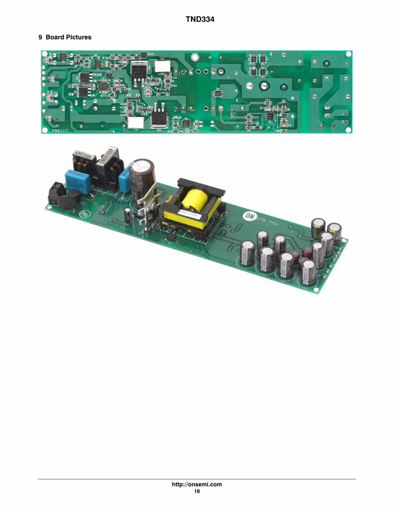
9 Board Pictures

TND334
http://onsemi.com19
10 Appendix
References:• ENERGY STAR®: Set--top boxes specificationhttp://www.energystar.gov/index.cfm?c=revisions.settop_box_spec
• EfficientProducts.org http ://www.efficientproducts.org/
Additional collateral from ON Semiconductor:• NCP1308: Current--Mode Controller for Free RunningQuasi--Resonant Operation
• NCP1587: Low Voltage Synchronous Buck Controller• TL431A: Programmable Precision Reference• MC79L05: 100 mA, 5 V, Negative Voltage Regulator• MMBT2222AW: General Purpose Transistor NPN• MMBT2907AW: General Purpose Transistor PNP• NTD4808N: Power MOSFET 30 V, 63 A, N--Channel• NTB60N06L: Power MOSFET 60 Amps, 60 Volts,Logic Level
• MURA110: 1 A, 100 V Ultrafast Rectifier• MMSD4148/D: 100 V Switching Diode• MMSZ5226B: Zener Diode 500 mW 3.3 V ±5%SOD--123
• Design note DN06008/D: NCP1308: ±18 V DualOutput Power Supply
• Application Note AND8129/D: A 30 W Power SupplyOperating in a Quasi--Square Wave Resonant Mode
• Application Note AND8089/D: Determining theFree--Running Frequency for QR Systems
• Application Note AND8252/D: High Efficiency 8Output, 60 W Set Top Box Power Supply Design
• GreenPoint® Reference Design TND332/D: 8 W DTAPower Supply Reference Design Documentation
ONSemiconductor and are registered trademarks of Semiconductor Components Industries, LLC (SCILLC). SCILLC reserves the right to make changes without further noticeto any products herein. SCILLCmakes nowarranty, representation or guarantee regarding the suitability of its products for any particular purpose, nor doesSCILLC assume any liabilityarising out of the application or use of any product or circuit, and specifically disclaims any and all liability, including without limitation special, consequential or incidental damages.“Typical” parameters which may be provided in SCILLC data sheets and/or specifications can and do vary in different applications and actual performance may vary over time. Alloperating parameters, including “Typicals”must be validated for each customer application by customer’s technical experts. SCILLC does not convey any license under its patent rightsnor the rights of others. SCILLC products are not designed, intended, or authorized for use as components in systems intended for surgical implant into the body, or other applicationsintended to support or sustain life, or for any other application in which the failure of the SCILLC product could create a situation where personal injury or death may occur. ShouldBuyer purchaseor useSCILLCproducts for any such unintendedor unauthorized application,Buyer shall indemnify andholdSCILLCand its officers, employees, subsidiaries, affiliates,and distributors harmless against all claims, costs, damages, and expenses, and reasonable attorney fees arising out of, directly or indirectly, any claim of personal injury or deathassociated with such unintended or unauthorized use, even if such claim alleges that SCILLC was negligent regarding the design or manufacture of the part. SCILLC is an EqualOpportunity/Affirmative Action Employer. This literature is subject to all applicable copyright laws and is not for resale in any manner.
PUBLICATION ORDERING INFORMATIONN. American Technical Support: 800--282--9855 Toll FreeUSA/CanadaEurope, Middle East and Africa Technical Support:Phone: 421 33 790 2910Japan Customer Focus CenterPhone: 81--3--5773--3850
TND334/D
GreenPoint is a registered trademark of Semiconductor Components Industries, LLC (SCILLC).
LITERATURE FULFILLMENT:Literature Distribution Center for ON SemiconductorP.O. Box 5163, Denver, Colorado 80217 USAPhone: 303--675--2175 or 800--344--3860 Toll Free USA/CanadaFax: 303--675--2176 or 800--344--3867 Toll Free USA/CanadaEmail: [email protected]
ON Semiconductor Website: www.onsemi.com
Order Literature: http://www.onsemi.com/orderlit
For additional information, please contact your localSales Representative