Embed Size (px)
Citation preview
TN-41-07: DDR3 Power-Up, Initialization, and ResetIntroduction
Technical NoteDDR3 Power-Up, Initialization, and Reset
IntroductionDDR3’s extensive feature set requires changes to the power-up and initialization routine for DDR3 SDRAM devices. Each time the memory is powered up, the device specifies a routine to initialize the internal state machines and to configure the numerous user-defined operating parameters. Although the routines for DDR3 are similar to those that are required in previous generations of DRAM, some differences do exist. The purpose of this technical note is to describe the differences in the power-up and initialization routines used by DDR3, to discuss the selectable modes that require special attention during initialization, and to introduce the RESET# pin and describe how to properly use it.
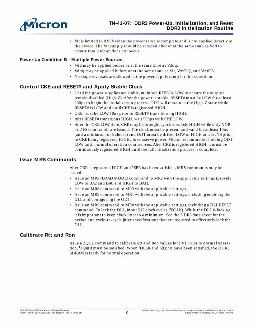
DDR3 Initialization RoutineThe following sequence of steps is required to power up and initialize the DDR3 SDRAM device. Following these steps will ensure that the part is in a known state prior to normal operation.
Apply Power
When power is ramped, the RESET# pin should be less than 0.2 × Vddq. Holding the RESET# pin LOW ensures that the outputs remain disabled (High-Z) and that ODT is off (Rtt is High-Z). Ensuring that Rtt is High-Z in DDR3 is one major difference between the DDR2 and DDR3 initialization routines. DDR2 requires that the ODT pin is held LOW after Vref is at a valid level, but DDR3 internally takes care of this when the RESET# pin is held LOW. RESET# is the only pin on the DDR3 device that operates with LVCMOS input levels. This enables it to internally be driven LOW independent of the voltage level of Vref. All other inputs may be undefined during this period.
During power-up, either condition A or condition B (described in the following para-graphs) must be met.
Power-Up Condition A – Single Power Source• Vdd and Vddq are driven from a single power converter output and are ramped with a
maximum delta voltage of 300mV. Slope reversal of any power supply signal is allowed. Although JEDEC supports slope reversal of the power supply in this specific condition, Micron recommends avoiding slope reversal if possible.
• To prevent latchup, the voltage levels on all balls except Vdd, Vddq, Vss, and Vssq must be less than or equal to Vddq and Vdd on one side and must be greater than or equal to Vssq and Vss on the other side. Both Vdd and Vddq power supplies must ramp to Vdd (MIN) and Vddq (MIN) within 200ms (tVddpr specification).
• Both VrefDQ and VrefCA track Vdd × 0.5. Note that VrefDQ and VrefCA are isolated within the DDR3 device and do not require separate external supplies.
PDF: 09005aef83713543/Source: 09005aef8361e0ae Micron Technology, Inc., reserves the right to change products or specifications without notice.tn4107_power_up_initialization_and_reset.fm - Rev. A 10/08 EN 1 ©2008 Micron Technology, Inc. All rights reserved.
Products and specifications discussed herein are for evaluation and reference purposes only and are subject to change by Micron without notice. Products are only warranted by Micron to meet Micron’s production data sheet specifications. All
information discussed herein is provided on an “as is” basis, without warranties of any kind.
TN-41-07: DDR3 Power-Up, Initialization, and ResetDDR3 Initialization Routine
• Vtt is limited to 0.95V when the power ramp is complete and is not applied directly to the device. The Vtt supply should be ramped after or at the same time as Vdd to ensure that latchup does not occur.
Power-Up Condition B – Multiple Power Sources• Vdd may be applied before or at the same time as Vddq.• Vddq may be applied before or at the same time as Vtt, VrefDQ, and VrefCA.• No slope reversals are allowed in the power supply ramp for this condition.
Control CKE and RESET# and Apply Stable Clock• Until the power supplies are stable, maintain RESET# LOW to ensure the outputs
remain disabled (High-Z). After the power is stable, RESET# must be LOW for at least 200µs to begin the initialization process. ODT will remain in the High-Z state while RESET# is LOW and until CKE is registered HIGH.
• CKE must be LOW 10ns prior to RESET# transitioning HIGH.• After RESET# transitions HIGH, wait 500µs with CKE LOW.• After the CKE LOW time, CKE may be brought synchronously HIGH while only NOP
or DES commands are issued. The clock must be present and valid for at least 10ns (and a minimum of 5 clocks) and ODT must be driven LOW or HIGH at least tIS prior to CKE being registered HIGH. To conserve power, Micron recommends holding ODT LOW until normal operation commences. After CKE is registered HIGH, it must be continuously registered HIGH until the full initialization process is complete.
Issue MRS Commands
After CKE is registered HIGH and tXPR has been satisfied, MRS commands may be issued. • Issue an MRS (LOAD MODE) command to MR2 with the applicable settings (provide
LOW to BA2 and BA0 and HIGH to BA1). • Issue an MRS command to MR3 with the applicable settings.• Issue an MRS command to MR1 with the applicable settings, including enabling the
DLL and configuring the ODT.• Issue an MRS command to MR0 with the applicable settings, including a DLL RESET
command. To lock the DLL, input 512 clock cycles (tDLLK). While the DLL is locking, it is important to keep clock jitter to a minimum. See the DDR3 data sheet for the period and cycle-to-cycle jitter specifications that are required to effectively lock the DLL.
Calibrate Rtt and Ron
Issue a ZQCL command to calibrate Rtt and Ron values for PVT. Prior to normal opera-tion, tZQinit must be satisfied. When tDLLK and tZQinit have been satisfied, the DDR3 SDRAM is ready for normal operation.
PDF: 09005aef83713543/Source: 09005aef8361e0ae Micron Technology, Inc., reserves the right to change products or specifications without notice.tn4107_power_up_initialization_and_reset.fm - Rev. A 10/08 EN 2 ©2008 Micron Technology, Inc. All rights reserved.
TN-41-07: DDR3 Power-Up, Initialization, and ResetDDR3 Initialization Routine
Figure 1: Initialization Routine
CKE
Rtt
BA[2:0]
All voltagesupplies validand stable
T = 200µs (MIN)
DM
DQS
Address
A10
CK
CK#
tCL
Command NOP
T0 Ta0
Don’t Care
tCL
tIS
tCK
ODT
DQ
Tb0
tDLLK
MR1 withDLL enable
MR0 withDLL reset
tMRD tMOD
MRSMRS
BA0 = HBA1 = LBA2 = L
BA0 = LBA1 = LBA2 = L
Code Code
Code Code
Valid
Valid
Valid
Valid
Normaloperation
MR2 MR3
tMRD tMRD
MRSMRS
BA0 = LBA1 = HBA2 = L
BA0 = HBA1 = HBA2 = L
Code Code
Code Code
Tc0 Td0
Vtt
Vref
Vddq
Vdd
RST#
T = 500µs (MIN)
tCKSRX
Stable andvalid clock
Valid
Power-upramp
T (MAX) = 200ms
DRAM ready for external commands
T1
tZQinit
ZQ calibration
A10 = H
ZQCL
tIS
See power-upconditions
in the initializationroutine text
tXPR
Valid
= 20nstIOz
Indicates a break in time scale
T (MIN) = 10ns
PDF: 09005aef83713543/Source: 09005aef8361e0ae Micron Technology, Inc., reserves the right to change products or specifications without notice.tn4107_power_up_initialization_and_reset.fm - Rev. A 10/08 EN 3 ©2008 Micron Technology, Inc. All rights reserved.

TN-41-07: DDR3 Power-Up, Initialization, and ResetDDR3 Initialization Routine
Figure 2: Initialization Flowchart
Vdd and Vddq ramp
Apply Vtt and Vref
Step
1
2
3
4
5
6
7
8
9
10
11
12
13
14
15
16
17
18
19
20
21
22
23
Hold RESET# below 0.2 x Vddq during voltage ramp
Hold RESET# LOW for at least 200μs
Bring CKE LOW at least 10ns prior to Step 6
Bring RESET# HIGH
Hold CKE LOW for at least 500μs
Assert NOP or DES on command bus
Apply stable clocks
Drive ODT LOW or HIGH
Wait at least 10ns (and minimum of 5 clocks)
Bring CKE HIGH
Wait at least tXPR
Wait at least tMRD
Wait at least tMRD
Wait at least tMRD
Wait at least tMOD
Issue a ZQCL command to calibrate Rtt and Ron
Satisfy tDLLK and tZQINIT timing
24 DRAM is ready for normal operation
Issue an MRS command to MR2
Issue an MRS command to MR3
Issue an MRS command to MR1
Issue an MRS command to MR0
PDF: 09005aef83713543/Source: 09005aef8361e0ae Micron Technology, Inc., reserves the right to change products or specifications without notice.tn4107_power_up_initialization_and_reset.fm - Rev. A 10/08 EN 4 ©2008 Micron Technology, Inc. All rights reserved.
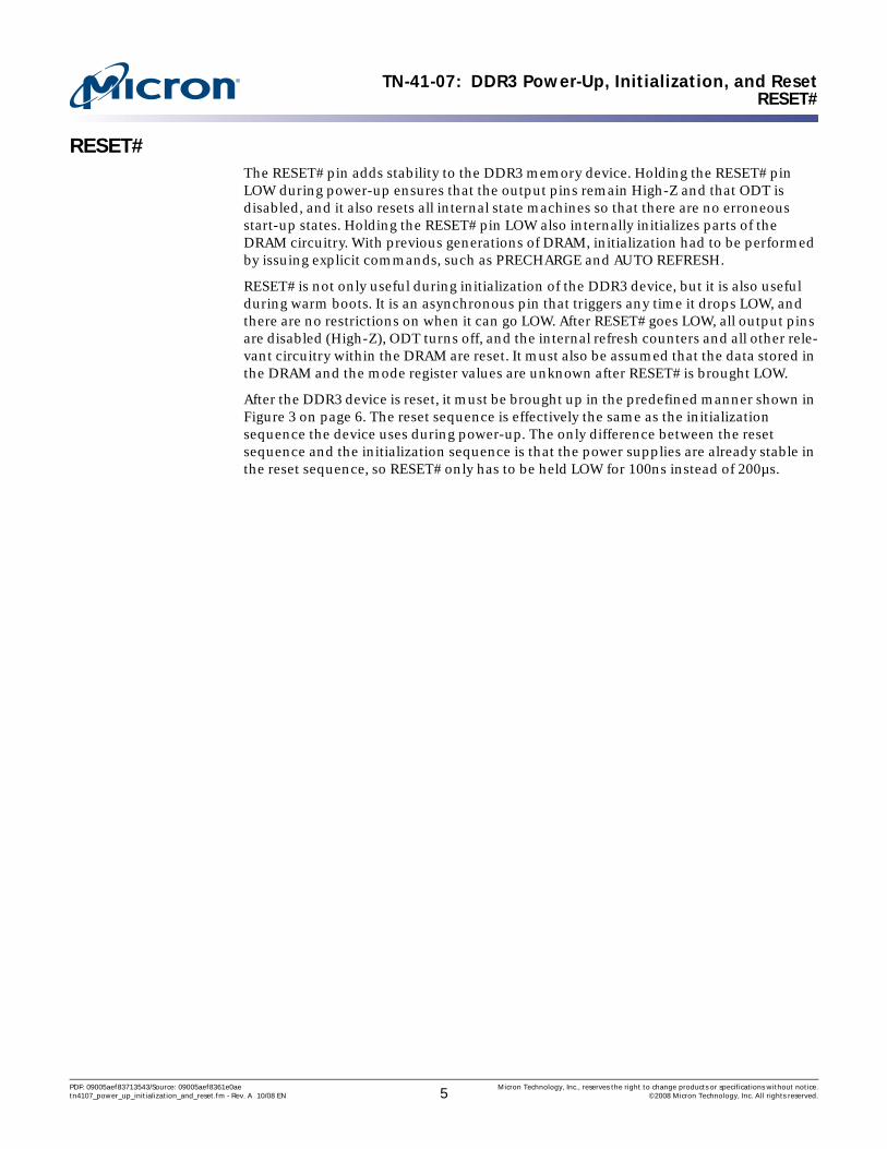
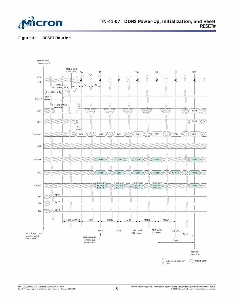
TN-41-07: DDR3 Power-Up, Initialization, and ResetRESET#
RESET#The RESET# pin adds stability to the DDR3 memory device. Holding the RESET# pin LOW during power-up ensures that the output pins remain High-Z and that ODT is disabled, and it also resets all internal state machines so that there are no erroneous start-up states. Holding the RESET# pin LOW also internally initializes parts of the DRAM circuitry. With previous generations of DRAM, initialization had to be performed by issuing explicit commands, such as PRECHARGE and AUTO REFRESH.
RESET# is not only useful during initialization of the DDR3 device, but it is also useful during warm boots. It is an asynchronous pin that triggers any time it drops LOW, and there are no restrictions on when it can go LOW. After RESET# goes LOW, all output pins are disabled (High-Z), ODT turns off, and the internal refresh counters and all other rele-vant circuitry within the DRAM are reset. It must also be assumed that the data stored in the DRAM and the mode register values are unknown after RESET# is brought LOW.
After the DDR3 device is reset, it must be brought up in the predefined manner shown in Figure 3 on page 6. The reset sequence is effectively the same as the initialization sequence the device uses during power-up. The only difference between the reset sequence and the initialization sequence is that the power supplies are already stable in the reset sequence, so RESET# only has to be held LOW for 100ns instead of 200µs.
PDF: 09005aef83713543/Source: 09005aef8361e0ae Micron Technology, Inc., reserves the right to change products or specifications without notice.tn4107_power_up_initialization_and_reset.fm - Rev. A 10/08 EN 5 ©2008 Micron Technology, Inc. All rights reserved.
TN-41-07: DDR3 Power-Up, Initialization, and ResetRESET#
Figure 3: RESET Routine
CKE
Rtt
BA[2:0]
All voltagesupplies validand stable
High-Z
DM
DQSHigh-Z
Address
A10
CK
CK#
tCL
Command NOP
T0 Ta0
Don’t Care
tCL
tIS
ODT
DQ High-Z
Tb0
tDLLK
MR1 with DLL enable
MRSMRS
BA0 = H BA1 = L BA2 = L
BA0 = L BA1 = L BA2 = L
Code Code
Code Code
Valid
Valid
Valid
Valid
Normal operation
MR2 MR3
MRSMRS
BA0 = L BA1 = H BA2 = L
BA0 = H BA1 = H BA2 = L
Code Code
Code Code
Tc0 Td0
RESET#
Stable andvalid clock
Valid
DRAM readyfor external commands
T1
tZQinit
A10 = H
ZQCL
tIS
tIOZ
Valid
System reset(warm boot)
ZQ CALMR0 withDLL reset
T = 10ns (MIN)
T = 100ns (MIN)
Indicates a break intime
T = 500μs (MIN) tXPR tMRD tMRD tMRD tMOD
T (MIN) =MAX (10ns, 5tCK)
tCK
PDF: 09005aef83713543/Source: 09005aef8361e0ae Micron Technology, Inc., reserves the right to change products or specifications without notice.tn4107_power_up_initialization_and_reset.fm - Rev. A 10/08 EN 6 ©2008 Micron Technology, Inc. All rights reserved.

TN-41-07: DDR3 Power-Up, Initialization, and ResetMode Registers
Mode RegistersLoading the configurable operating parameters into the DDR3 device is performed simi-larly to the way that configurable operating parameters are loaded in previous genera-tions of DRAM. The DDR3 nomenclature for mode register sets is different than DDR2; for example, DDR2 devices name all mode registers that are beyond the base register as extended registers, and DDR3 devices do not. Regardless of the name differences, many of the modes operate the same way. For more information about available modes, refer to the DDR3 data sheets available on Micron’s Web site.
JEDEC defines the sequence in which the mode registers are loaded during the initializa-tion routine (MR2 followed by MR3, MR1, and MR0). Micron tests DDR3 devices using the routine defined by JEDEC and recommends that users follow the same methodology. The mode registers in DDR3 that require special consideration during initialization are discussed in the following sections.
Mode Register 0 (MR0)
The DDR3 base register, mode register 0 (MR0), has effectively the same type of func-tions as DDR2. These modes include burst length (BL), READ burst type, CAS latency, DLL reset, write recovery (WR), and precharge power-down (PD).
It is important to note that when initializing the DRAM, the DLL must be enabled with MR1 prior to performing the DLL reset in MR0. When the DLL reset bit is enabled, CKE must be HIGH, and the input clock must be held stable for 512 (tDLLK) clock cycles before a READ command can be issued.
Figure 4: MR0 Definition
Notes: 1. MR0[16, 13, 7, 2] are reserved for future use and must be programmed to 0.
01 BLCAS latency BTPD
A9 A7 A6 A5 A4 A3 0A1A2A8A
Mode register 0 (MR0)
Address bus
9 7 6 5 4 3 0128
A10A12 A11BA0BA1
10111213
M3
0
1
READ Burst Type
Sequential (nibble)
Interleaved
CAS Latency
Reserved
5
6
7
8
9
10
11 (DDR3-1600)
M4
0
1
0
1
0
1
0
1
M5
0
0
1
1
0
0
1
1
M6
0
0
0
0
1
1
1
1
15DLL
Write Recovery
Reserved
5
6
7
8
10
12
Reserved
WR00
M12
0
1
Precharge PD
DLL off (slow exit)
DLL on (fast exit)
BA2
16
01
Burst Length
Fixed BL8
4 or 8 (on-the-fly via A12)
Fixed BC4 (chop)
Reserved
M0
0
1
0
1
M1
0
0
1
1
M9
0
1
0
1
0
1
0
1
M10
0
0
1
1
0
0
1
1
M11
0
0
0
0
1
1
1
1
M14
0
1
0
1
M15
0
0
1
1
Mode Register
Mode register 0 (MR0)
Mode register 1 (MR1)
Mode register 2 (MR2)
Mode register 3 (MR3)
A13
14
01 01
M8
0
1
DLL Reset
No
Yes
PDF: 09005aef83713543/Source: 09005aef8361e0ae Micron Technology, Inc., reserves the right to change products or specifications without notice.tn4107_power_up_initialization_and_reset.fm - Rev. A 10/08 EN 7 ©2008 Micron Technology, Inc. All rights reserved.
TN-41-07: DDR3 Power-Up, Initialization, and ResetMode Registers
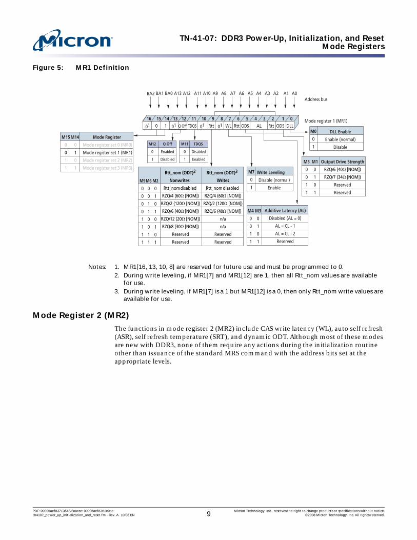
Mode Register 1 (MR1)
The functions available in mode register 1 (MR1) include DLL enable/disable, output drive strength (ODS), CAS additive latency (AL), write leveling (WL), Rtt_nom value (ODT), TDQS, and Q off (output disable).
To obtain the tight tolerances of the output drive impedance and Rtt_nom values that are selected in MR1, it is necessary to perform the ZQ CALIBRATION LONG (ZQCL) command during the initialization routine. After ZQCL is issued, the tZQinit timing parameter must be met. During this time, only NOP and DES commands may be issued to the DDR3 device. However, the DLL locking time, also 512 clocks, may be performed in parallel with the ZQ calibration.
For improved signal integrity, DDR3 modules have incorporated a fly-by topology for the address, command, and clock signals. With this new topology, an inherent skew between the DQS and CK must be overcome. Write leveling, a feature in MR1, uses feedback to overcome skew during the initialization routine. Because the write-leveling mode register interacts with many of the other mode registers, it is intended for use after all the other programmable features in mode registers 0–3 are set, and the DLL is fully reset and locked. For more information about how to use write leveling, refer to the DDR3 data sheets available on Micron’s Web site.
After the DQS and CK signals for the DDR3 device are aligned, certain steps, which are explained in the DDR3 data sheets, must be performed prior to normal operation. Other than reloading MR1 to turn off write leveling, no other mode registers need to be reloaded prior to normal operation.
PDF: 09005aef83713543/Source: 09005aef8361e0ae Micron Technology, Inc., reserves the right to change products or specifications without notice.tn4107_power_up_initialization_and_reset.fm - Rev. A 10/08 EN 8 ©2008 Micron Technology, Inc. All rights reserved.
TN-41-07: DDR3 Power-Up, Initialization, and ResetMode Registers
Figure 5: MR1 Definition
Notes: 1. MR1[16, 13, 10, 8] are reserved for future use and must be programmed to 0.2. During write leveling, if MR1[7] and MR1[12] are 1, then all Rtt_nom values are available
for use.3. During write leveling, if MR1[7] is a 1 but MR1[12] is a 0, then only Rtt_nom write values are
available for use.
Mode Register 2 (MR2)
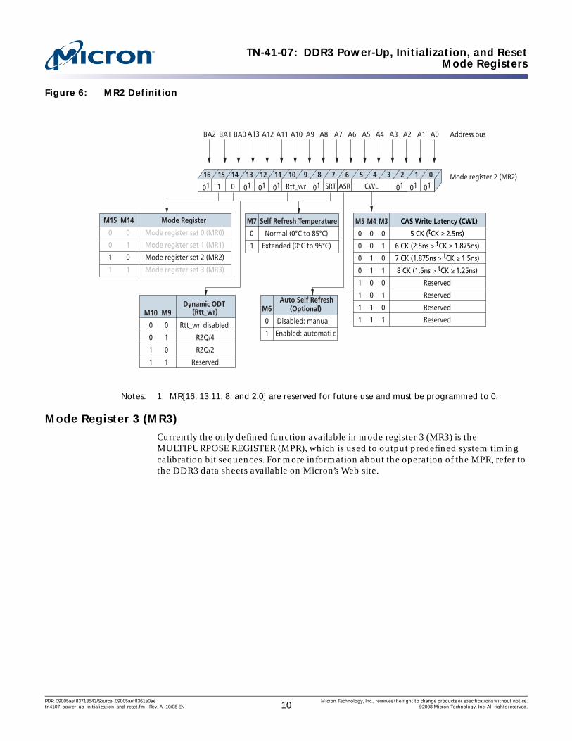
The functions in mode register 2 (MR2) include CAS write latency (WL), auto self refresh (ASR), self refresh temperature (SRT), and dynamic ODT. Although most of these modes are new with DDR3, none of them require any actions during the initialization routine other than issuance of the standard MRS command with the address bits set at the appropriate levels.
AL RttQ Off
A9 A7 A6 A5 A4 A3 0A1A2A8A
Mode register 1 (MR1)
Address bus
9 7 6 5 4 3 0128
A10A12 A11BA0BA1
10111213
M0
0
1
DLL Enable
Enable (normal)
Disable
M5
0
0
1
1
Output Drive Strength
RZQ/6 (40Ω [NOM])
RZQ/7 (34Ω [NOM])
Reserved
Reserved
14
WL1 SDO0 DLLRttTDQS
M12
0
1
Q Off
Enabled
Disabled
BA2
15
01
M7
0
1
Write Leveling
Disable (normal)
Enable
Additive Latency (AL)
Disabled (AL = 0)
AL = CL - 1
AL = CL - 2
Reserved
M3
0
1
0
1
M4
0
0
1
1
Rtt ODS
M1
0
1
0
1
A13
16
01
M11
0
1
TDQS
Disabled
Enabled
01 01
Rtt_nom (ODT)2
Nonwrites
Rtt_nom disabled
RZQ/4 (60Ω [NOM])
RZQ/2 (120Ω [NOM])
RZQ/6 (40Ω [NOM])
RZQ/12 (20Ω [NOM])
RZQ/8 (30Ω [NOM])
Reserved
Reserved
(ODT)3
Writes
disabled
RZQ/4 (60Ω [NOM])
RZQ/2 (120Ω [NOM])
RZQ/6 (40Ω [NOM])
n/a
n/a
Reserved
Reserved
M2
0
1
0
1
0
1
0
1
M6
0
0
1
1
0
0
1
1
M9
0
0
0
0
1
1
1
1
Mode Register
Mode register set 0 (MR0)
Mode register set 1 (MR1)
Mode register set 2 (MR2)
Mode register set 3 (MR3)
M14
0
1
0
1
M15
0
0
1
1Rtt_nom
Rtt_nom
PDF: 09005aef83713543/Source: 09005aef8361e0ae Micron Technology, Inc., reserves the right to change products or specifications without notice.tn4107_power_up_initialization_and_reset.fm - Rev. A 10/08 EN 9 ©2008 Micron Technology, Inc. All rights reserved.
TN-41-07: DDR3 Power-Up, Initialization, and ResetMode Registers
Figure 6: MR2 Definition
Notes: 1. MR[16, 13:11, 8, and 2:0] are reserved for future use and must be programmed to 0.
Mode Register 3 (MR3)
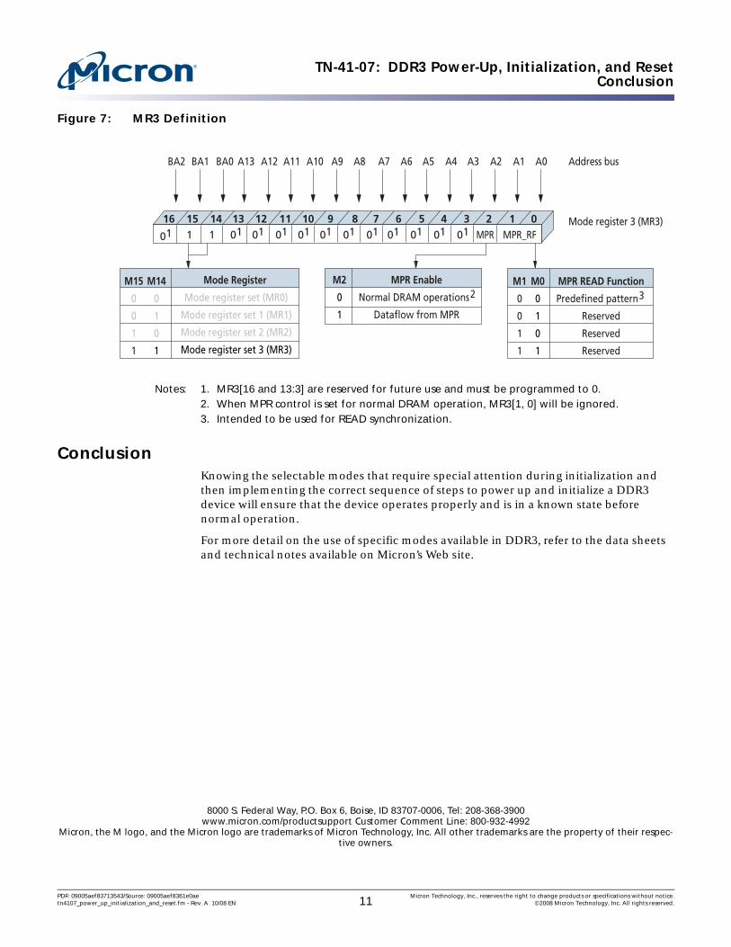
Currently the only defined function available in mode register 3 (MR3) is the MULTIPURPOSE REGISTER (MPR), which is used to output predefined system timing calibration bit sequences. For more information about the operation of the MPR, refer to the DDR3 data sheets available on Micron’s Web site.
M14
0
1
0
1
M15
0
0
1
1
Mode Register
Mode register set 0 (MR0)
Mode register set 1 (MR1)
Mode register set 2 (MR2)
Mode register set 3 (MR3)
A9 A7 A6 A5 A4 A3 0A1A2A8A
Mode register 2 (MR2)
Address bus
9 7 6 5 4 38 2 1 0
A10A12 A11BA0BA1
101112131415
1 CWL010
BA2
ASR
16
01
A13
01 01 01 01 0101 SRTRtt_wr
M6
0
1
Auto Self Refresh(Optional)
Disabled: manual
Enabled: automati c
M7
0
1
Self Refresh Temperature
Normal (0°C to 85°C)
Extended (0°C to 95°C)
CAS Write Latency (CWL)
5 CK (tCK ≥ 2.5ns)
6 CK (2.5ns > tCK ≥ 1.875ns)
7 CK (1.875ns > tCK ≥ 1.5ns)
8 CK (1.5ns > tCK ≥ 1.25ns)
Reserved
Reserved
Reserved
Reserved
M3
0
1
0
1
0
1
0
1
M4
0
0
1
1
0
0
1
1
M5
0
0
0
0
1
1
1
1M9
0
1
0
1
M10
0
0
1
1
Dynamic ODT
disabled
RZQ/4
RZQ/2
Reserved
Rtt_wr
(Rtt_wr)
PDF: 09005aef83713543/Source: 09005aef8361e0ae Micron Technology, Inc., reserves the right to change products or specifications without notice.tn4107_power_up_initialization_and_reset.fm - Rev. A 10/08 EN 10 ©2008 Micron Technology, Inc. All rights reserved.
TN-41-07: DDR3 Power-Up, Initialization, and ResetConclusion
Figure 7: MR3 Definition
Notes: 1. MR3[16 and 13:3] are reserved for future use and must be programmed to 0.2. When MPR control is set for normal DRAM operation, MR3[1, 0] will be ignored.3. Intended to be used for READ synchronization.
ConclusionKnowing the selectable modes that require special attention during initialization and then implementing the correct sequence of steps to power up and initialize a DDR3 device will ensure that the device operates properly and is in a known state before normal operation.
For more detail on the use of specific modes available in DDR3, refer to the data sheets and technical notes available on Micron’s Web site.
A9 A7 A6 A5 A4 A3 0A1A2A8A
Mode register 3 (MR3)
Address bus
9 7 6 5 4 38 2 1 0
A10A12 A11BA0BA1
101112131415
A13
1 01 01 01 01 01 01 01 MPR1
BA2
16
01 01 01 01 01
M2
0
1
MPR Enable
Normal DRAM operations2
Dataflow from MPR
MPR_RF
M14
0
1
0
1
M15
0
0
1
1
Mode Register
Mode register set (MR0)
Mode register set 1 (MR1)
Mode register set 2 (MR2)
Mode register set 3 (MR3)
MPR READ Function
Predefined pattern3
Reserved
Reserved
Reserved
M0
0
1
0
1
M1
0
0
1
1
8000 S. Federal Way, P.O. Box 6, Boise, ID 83707-0006, Tel: 208-368-3900www.micron.com/productsupport Customer Comment Line: 800-932-4992
Micron, the M logo, and the Micron logo are trademarks of Micron Technology, Inc. All other trademarks are the property of their respec-tive owners.
PDF: 09005aef83713543/Source: 09005aef8361e0ae Micron Technology, Inc., reserves the right to change products or specifications without notice.tn4107_power_up_initialization_and_reset.fm - Rev. A 10/08 EN 11 ©2008 Micron Technology, Inc. All rights reserved.

TN-41-07: DDR3 Power-Up, Initialization, and ResetRevision History
Revision HistoryRev. A . . . . . . . . . . . . . . . . . . . . . . . . . . . . . . . . . . . . . . . . . . . . . . . . . . . . . . . . . . . . . . . . . . . . . . . . . . . . . . . . . . . . . . . . . . . . . .10/08
• Initial release
PDF: 09005aef83713543/Source: 09005aef8361e0ae Micron Technology, Inc., reserves the right to change products or specifications without notice.tn4107_power_up_initialization_and_reset.fm - Rev. A 10/08 EN 12 ©2008 Micron Technology, Inc. All rights reserved.