Embed Size (px)
Citation preview

www.ti.com
1 Digital Media System-on-Chip (DMSoC)
1.1 Features
TMS320DM6446Digital Media System-on-Chip
SPRS283E–DECEMBER 2005–REVISED MARCH 2007
• High-Performance Digital Media SoC • ARM926EJ-S Core– 594-MHz C64x+™ Clock Rate – Support for 32-Bit and 16-Bit (Thumb®
Mode) Instruction Sets– 297-MHz ARM926EJ-S™ Clock Rate– DSP Instruction Extensions and Single– Eight 32-Bit C64x+ Instructions/Cycle
Cycle MAC– 4752 C64x+ MIPS– ARM® Jazelle® Technology– Fully Software-Compatible With C64x /– EmbeddedICE-RT™ Logic for Real-TimeARM9™
Debug• Advanced Very-Long-Instruction-Word (VLIW)• ARM9 Memory ArchitectureTMS320C64x+™ DSP Core
– 16K-Byte Instruction Cache– Eight Highly Independent Functional Units– 8K-Byte Data Cache• Six ALUs (32-/40-Bit), Each Supports– 16K-Byte RAMSingle 32-Bit, Dual 16-Bit, or Quad 8-Bit
Arithmetic per Clock Cycle – 8K-Byte ROM• Two Multipliers Support Four 16 x 16-Bit • Embedded Trace Buffer™ (ETB11™) With 4KB
Multiplies (32-Bit Results) per Clock Memory for ARM9 DebugCycle or Eight 8 x 8-Bit Multiplies (16-Bit
• Endianness: Little Endian for ARM and DSPResults) per Clock Cycle• Video Processing Subsystem– Load-Store Architecture With Non-Aligned
– Front End Provides:Support• CCD and CMOS Imager Interface– 64 32-Bit General-Purpose Registers• BT.601/BT.656 Digital YCbCr 4:2:2– Instruction Packing Reduces Code Size
(8-/16-Bit) Interface– All Instructions Conditional• Preview Engine for Real-Time Image– Additional C64x+™ Enhancements
Processing• Protected Mode Operation• Glueless Interface to Common Video• Exceptions Support for Error Detection
Decodersand Program Redirection• Histogram Module• Hardware Support for Modulo Loop• Auto-Exposure, Auto-White Balance andOperation
Auto-Focus Module• C64x+ Instruction Set Features• Resize Engine
– Byte-Addressable (8-/16-/32-/64-Bit Data)• Resize Images From 1/4x to 4x
– 8-Bit Overflow Protection• Separate Horizontal/Vertical Control
– Bit-Field Extract, Set, Clear– Back End Provides:
– Normalization, Saturation, Bit-Counting• Hardware On-Screen Display (OSD)
– Compact 16-Bit Instructions• Four 54-MHz DACs for a Combination of
– Additional Instructions to Support Complex• Composite NTSC/PAL VideoMultiplies• Luma/Chroma Separate Video• C64x+ L1/L2 Memory Architecture (S-video)
– 32K-Byte L1P Program RAM/Cache (Direct • Component (YPbPr or RGB) VideoMapped) (Progressive)– 80K-Byte L1D Data RAM/Cache (2-Way • Digital OutputSet-Associative)
• 8-/16-bit YUV or up to 24-Bit RGB– 64K-Byte L2 Unified Mapped RAM/Cache• HD Resolution(Flexible RAM/Cache Allocation)• Up to 2 Video Windows
Please be aware that an important notice concerning availability, standard warranty, and use in critical applications of TexasInstruments semiconductor products and disclaimers thereto appears at the end of this document.
All trademarks are the property of their respective owners.
PRODUCTION DATA information is current as of publication date. Copyright © 2005–2007, Texas Instruments IncorporatedProducts conform to specifications per the terms of the TexasInstruments standard warranty. Production processing does notnecessarily include testing of all parameters.

www.ti.com
1.2 Description
TMS320DM6446Digital Media System-on-ChipSPRS283E–DECEMBER 2005–REVISED MARCH 2007
• External Memory Interfaces (EMIFs) – IEEE 802.3 Compliant– 32-Bit DDR2 SDRAM Memory Controller – Media Independent Interface (MII)
With 256M-Byte Address Space (1.8-V I/O) • VLYNQ™ Interface (FPGA Interface)– Asynchronous16-Bit Wide EMIF (EMIFA) • Host Port Interface (HPI) with 16-Bit
With 128M-Byte Address ReachMultiplexed Address/Data
• Flash Memory Interfaces• USB Port With Integrated 2.0 PHY• NOR (8-/16-Bit-Wide Data)
– USB 2.0 High-/Full-Speed (480-Mbps) Client• NAND (8-/16-Bit-Wide Data)– USB 2.0 High-/Full-/Low-Speed Host
• Flash Card Interfaces (Mini-Host, Supporting One External– Multimedia Card (MMC)/Secure Digital (SD) Device)
with Secure Data I/O (SDIO) • Three Pulse Width Modulator (PWM) Outputs– Compact Flash Controller With True IDE
• On-Chip ARM ROM Bootloader (RBL) to BootModeFrom NAND Flash or UART– SmartMedia
• ATA/ATAPI I/F (ATA/ATAPI-6 Specification)• Enhanced Direct-Memory-Access (EDMA)• Individual Power-Saving Modes for ARM/DSPController (64 Independent Channels)• Flexible PLL Clock Generators• Two 64-Bit General-Purpose Timers (Each
Configurable as Two 32-Bit Timers) • IEEE-1149.1 (JTAG) Boundary-Scan-Compatible• One 64-Bit Watch Dog Timer
• Up to 71 General-Purpose I/O (GPIO) Pins• Three UARTs (One with RTS and CTS Flow(Multiplexed With Other Device Functions)Control)
• 361-Pin Pb-Free BGA Package• One Serial Port Interface (SPI) With Two(ZWT Suffix), 0.8-mm Ball PitchChip-Selects
• 0.09-µm/6-Level Cu Metal Process (CMOS)• Master/Slave Inter-Integrated Circuit (I2CBus™) • 3.3-V and 1.8-V I/O, 1.2-V Internal
• Audio Serial Port (ASP) • Applications:– I2S – Digital Media– AC97 Audio Codec Interface – Networked Media Encode/Decode– Standard Voice Codec Interface (AIC12) – Video Imaging
• 10/100 Mb/s Ethernet MAC (EMAC)
The TMS320DM6446 (also referenced as DM6446) leverages TI’s DaVinci™ technology to meet thenetworked media encode and decode application processing needs of next-generation embedded devices.
The DM6446 enables OEMs and ODMs to quickly bring to market devices featuring robust operatingsystems support, rich user interfaces, high processing performance, and long battery life through themaximum flexibility of a fully integrated mixed processor solution.
The dual-core architecture of the DM6446 provides benefits of both DSP and Reduced Instruction SetComputer (RISC) technologies, incorporating a high-performance TMS320C64x+ DSP core and anARM926EJ-S core.
The ARM926EJ-S is a 32-bit RISC processor core that performs 32-bit or 16-bit instructions andprocesses 32-bit, 16-bit, or 8-bit data. The core uses pipelining so that all parts of the processor andmemory system can operate continuously.
The ARM core incorporates:• A coprocessor 15 (CP15) and protection module• Data and program Memory Management Units (MMUs) with table look-aside buffers.• Separate 16K-byte instruction and 8K-byte data caches. Both are four-way associative with virtual
index virtual tag (VIVT).
Digital Media System-on-Chip (DMSoC)2 Submit Documentation Feedback

www.ti.com
TMS320DM6446Digital Media System-on-Chip
SPRS283E–DECEMBER 2005–REVISED MARCH 2007
The TMS320C64x+™ DSPs are the highest-performance fixed-point DSP generation in theTMS320C6000™ DSP platform. It is based on an enhanced version of the second-generationhigh-performance, advanced very-long-instruction-word (VLIW) architecture developed by TexasInstruments (TI), making these DSP cores an excellent choice for digital media applications. The C64x is acode-compatible member of the C6000™ DSP platform. The TMS320C64x+ DSP is an enhancement ofthe C64x+ DSP with added functionality and an expanded instruction set.
Any reference to the C64x DSP or C64x CPU also applies, unless otherwise noted, to the C64x+ DSP andC64x+ CPU, respectively.
With performance of up to 4752 million instructions per second (MIPS) at a clock rate of 594 MHz, theC64x+ core offers solutions to high-performance DSP programming challenges. The DSP core possessesthe operational flexibility of high-speed controllers and the numerical capability of array processors. TheC64x+ DSP core processor has 64 general-purpose registers of 32-bit word length and eight highlyindependent functional units—two multipliers for a 32-bit result and six arithmetic logic units (ALUs). Theeight functional units include instructions to accelerate the performance in video and imaging applications.The DSP core can produce four 16-bit multiply-accumulates (MACs) per cycle for a total of 2376 millionMACs per second (MMACS), or eight 8-bit MACs per cycle for a total of 4752 MMACS. For more detailson the C64x+ DSP, see the TMS320C64x/C64x+ DSP CPU and Instruction Set Reference Guide(literature number SPRU732).
The DM6446 also has application-specific hardware logic, on-chip memory, and additional on-chipperipherals similar to the other C6000 DSP platform devices. The DM6446 core uses a two-levelcache-based architecture. The Level 1 program cache (L1P) is a 256K-bit direct mapped cache and theLevel 1 data cache (L1D) is a 640K-bit 2-way set-associative cache. The Level 2 memory/cache (L2)consists of an 512K-bit memory space that is shared between program and data space. L2 memory canbe configured as mapped memory, cache, or combinations of the two.
The peripheral set includes: 2 configurable video ports; a 10/100 Mb/s Ethernet MAC (EMAC) with aManagement Data Input/Output (MDIO) module; an inter-integrated circuit (I2C) Bus interface; one audioserial port (ASP); 2 64-bit general-purpose timers each configurable as 2 independent 32-bit timers;1 64-bit watchdog timer; up to 71-pins of general-purpose input/output (GPIO) with programmableinterrupt/event generation modes, multiplexed with other peripherals; 3 UARTs with hardwarehandshaking support on 1 UART; 3 pulse width modulator (PWM) peripherals; and 2 external memoryinterfaces: an asynchronous external memory interface (EMIFA) for slower memories/peripherals, and ahigher speed synchronous memory interface for DDR2.
The DM6446 device includes a Video Processing Subsystem (VPSS) with two configurable video/imagingperipherals: 1 Video Processing Front-End (VPFE) input used for video capture, 1 Video ProcessingBack-End (VPBE) output with imaging co-processor (VICP) used for display.
The Video Processing Front-End (VPFE) is comprised of a CCD Controller (CCDC), a Preview Engine(Previewer), Histogram Module, Auto-Exposure/White Balance/Focus Module (H3A), and Resizer. TheCCDC is capable of interfacing to common video decoders, CMOS sensors, and Charge Coupled Devices(CCDs). The Previewer is a real-time image processing engine that takes raw imager data from a CMOSsensor or CCD and converts from an RGB Bayer Pattern to YUV4:2:2. The Histogram and H3A modulesprovide statistical information on the raw color data for use by the DM6446. The Resizer accepts imagedata for separate horizontal and vertical resizing from 1/4x to 4x in increments of 256/N, where N isbetween 64 and 1024.
The Video Processing Back-End (VPBE) is comprised of an On-Screen Display Engine (OSD) and aVideo Encoder (VENC). The OSD engine is capable of handling 2 separate video windows and 2 separateOSD windows. Other configurations include 2 video windows, 1 OSD window, and 1 attribute windowallowing up to 8 levels of alpha blending. The VENC provides four analog DACs that run at 54 MHz,providing a means for composite NTSC/PAL video, S-Video, and/or Component video output. The VENCalso provides up to 24 bits of digital output to interface to RGB888 devices. The digital output is capable of8/16-bit BT.656 output and/or CCIR.601 with separate horizontal and vertical syncs.
Submit Documentation Feedback Digital Media System-on-Chip (DMSoC) 3

www.ti.com
TMS320DM6446Digital Media System-on-ChipSPRS283E–DECEMBER 2005–REVISED MARCH 2007
The Ethernet Media Access Controller (EMAC) provides an efficient interface between the DM644x andthe network. The DM6446 EMAC support both 10Base-T and 100Base-TX, or 10 Mbits/second (Mbps)and 100 Mbps in either half- or full-duplex mode, with hardware flow control and quality of service (QOS)support.
The Management Data Input/Output (MDIO) module continuously polls all 32 MDIO addresses in order toenumerate all PHY devices in the system. Once a PHY candidate has been selected by the ARM, theMDIO module transparently monitors its link state by reading the PHY status register. Link change eventsare stored in the MDIO module and can optionally interrupt the ARM, allowing the ARM to poll the linkstatus of the device without continuously performing costly MDIO accesses.
The HPI, I2C, SPI, USB2.0, and VLYNQ ports allow DM6446 to easily control peripheral devices and/orcommunicate with host processors. The DM6446 also provides multimedia card support, MMC/SD, withSDIO support.
The DM6446 also includes a Video/Imaging Co-processor (VICP) to offload many video and imagingprocessing tasks from the DSP core, making more DSP MIPS available for common video and imagingalgorithms. For more information on the VICP enhanced codecs, such as H.264 and MPEG4, pleasecontact your nearest TI sales representative.
The rich peripheral set provides the ability to control external peripheral devices and communicate withexternal processors. For details on each of the peripherals, see the related sections later in this documentand the associated peripheral reference guides.
The DM6446 has a complete set of development tools for both the ARM and DSP. These include Ccompilers, a DSP assembly optimizer to simplify programming and scheduling, and a Windows™debugger interface for visibility into source code execution.
Digital Media System-on-Chip (DMSoC)4 Submit Documentation Feedback

www.ti.com
1.3 Functional Block Diagram
JTAG Interface
System Control
PLLs/ClockGenerator
InputClock(s)
Power/SleepController
PinMultiplexing
ARM Subsystem
ARM926EJ-S CPU
16 KBI-Cache
16 KB RAM
8 KBD-Cache
16 KB ROM
DSP Subsystem
C64x+ DSP CPU
32 KBL1 Pgm
64 KB L2 RAM
80 KBL1 Data
Video-ImagingCoprocessor (VICP)
BT.656, Y/C,Raw (Bayer)
Video Processing Subsystem (VPSS)
CCDController
VideoInterface
Front End
Resizer
Histogram/3A
Preview
10b DACOn-Screen
Display(OSD)
VideoEncoder(VENC)
10b DAC
10b DAC
10b DAC
Back End 8b BT.656,Y/C,24b RGB
NTSC/PAL,S-Video,RGB,YPbPr
Switched Central Resource (SCR)
Peripherals
EDMA AudioSerialPort
I2C SPIUART
Serial Interfaces
DDR2Mem Ctlr(16b/32b)
Async EMIF/NAND/
SmartMedia
ATA/Compact
Flash
MMC/SD/
SDIO
Program/Data Storage
WatchdogTimer PWM
System
General-Purpose
Timer
USB 2.0PHY VLYNQ
EMACWith
MDIO
Connectivity
HPI
TMS320DM6446Digital Media System-on-Chip
SPRS283E–DECEMBER 2005–REVISED MARCH 2007
Figure 1-1 shows the functional block diagram of the device.
Figure 1-1. TMS320DM6446 Functional Block Diagram
Submit Documentation Feedback Digital Media System-on-Chip (DMSoC) 5

www.ti.com
Contents
TMS320DM6446Digital Media System-on-ChipSPRS283E–DECEMBER 2005–REVISED MARCH 2007
1 Digital Media System-on-Chip (DMSoC) ............ 1 6.1 Parameter Information .............................. 886.2 Recommended Clock and Control Signal Transition1.1 Features .............................................. 1
Behavior ............................................. 891.2 Description............................................ 26.3 Power Supplies...................................... 891.3 Functional Block Diagram ............................ 56.4 Reset ................................................ 98Revision History............................................... 76.5 External Clock Input From MXI/CLKIN Pin ........ 1022 Device Overview ......................................... 96.6 Clock PLLs ......................................... 1052.1 Device Characteristics................................ 96.7 Interrupts ........................................... 1122.2 Device Compatibility................................. 106.8 General-Purpose Input/Output (GPIO)............. 1192.3 ARM Subsystem .................................... 106.9 Enhanced Direct Memory Access (EDMA)2.4 DSP Subsystem ..................................... 14
Controller........................................... 1222.5 Memory Map Summary ............................. 18
6.10 External Memory Interface (EMIF)................. 1352.6 Pin Assignments .................................... 21
6.11 ATA/CF ............................................ 1432.7 Terminal Functions .................................. 26
6.12 MMC/SD/SDIO..................................... 1562.8 Device Support ...................................... 57
6.13 Video Processing Sub-System (VPSS) Overview . 1593 Device Configurations................................. 60
6.14 Host-Port Interface (HPI)........................... 1823.1 System Module Registers ........................... 60
6.15 USB 2.0 ............................................ 1853.2 Power Considerations ............................... 60 6.16 Universal Asynchronous Receiver/Transmitter3.3 Bootmode ........................................... 61 (UART) ............................................. 1943.4 Configurations at Reset ............................. 65 6.17 Serial Port Interface (SPI).......................... 1973.5 Configurations After Reset .......................... 69 6.18 Inter-Integrated Circuit (I2C) ....................... 2013.6 Emulation Control ................................... 81 6.19 Audio Serial Port (ASP)............................ 205
4 System Interconnect................................... 83 6.20 Ethernet Media Access Controller (EMAC) ........ 2094.1 System Interconnect Block Diagram ................ 84 6.21 Management Data Input/Output (MDIO)........... 216
5 Device Operating Conditions ........................ 85 6.22 Timer ............................................... 2185.1 Absolute Maximum Ratings Over Operating Case 6.23 Pulse Width Modulator (PWM)..................... 220
Temperature Range6.24 VLYNQ ............................................. 222(Unless Otherwise Noted) .......................... 856.25 IEEE 1149.1 JTAG ................................ 2265.2 Recommended Operating Conditions............... 86
7 Mechanical Packaging and Orderable5.3 Electrical Characteristics Over RecommendedInformation ............................................. 228Ranges of Supply Voltage and Operating Case
Temperature (Unless Otherwise Noted) ............ 87 7.1 Thermal Data for ZWT ............................. 2286 Peripheral and Electrical Specifications........... 88 7.1.1 Packaging Information............................. 228
Contents6 Submit Documentation Feedback
www.ti.com
Revision History
TMS320DM6446Digital Media System-on-Chip
SPRS283E–DECEMBER 2005–REVISED MARCH 2007
This data manual revision history highlights the technical changes made to the SPRS283D device-specificdata manual to make it an SPRS283E revision.
Scope: Applicable updates to the DM64x device family, specifically relating to the TMS320DM6446device, have been incorporated.
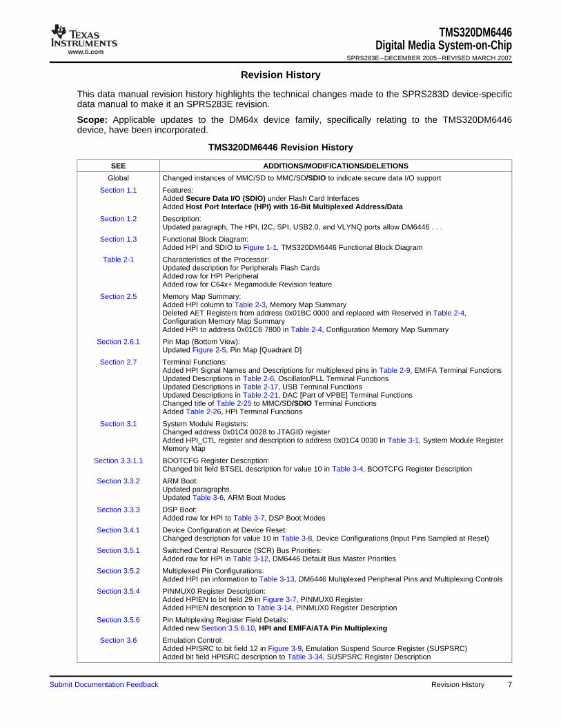
TMS320DM6446 Revision History
SEE ADDITIONS/MODIFICATIONS/DELETIONS
Global Changed instances of MMC/SD to MMC/SD/SDIO to indicate secure data I/O support
Section 1.1 Features:Added Secure Data I/O (SDIO) under Flash Card InterfacesAdded Host Port Interface (HPI) with 16-Bit Multiplexed Address/Data
Section 1.2 Description:Updated paragraph, The HPI, I2C, SPI, USB2.0, and VLYNQ ports allow DM6446 . . .
Section 1.3 Functional Block Diagram:Added HPI and SDIO to Figure 1-1, TMS320DM6446 Functional Block Diagram
Table 2-1 Characteristics of the Processor:Updated description for Peripherals Flash CardsAdded row for HPI PeripheralAdded row for C64x+ Megamodule Revision feature
Section 2.5 Memory Map Summary:Added HPI column to Table 2-3, Memory Map SummaryDeleted AET Registers from address 0x01BC 0000 and replaced with Reserved in Table 2-4,Configuration Memory Map SummaryAdded HPI to address 0x01C6 7800 in Table 2-4, Configuration Memory Map Summary
Section 2.6.1 Pin Map (Bottom View):Updated Figure 2-5, Pin Map [Quadrant D]
Section 2.7 Terminal Functions:Added HPI Signal Names and Descriptions for multiplexed pins in Table 2-9, EMIFA Terminal FunctionsUpdated Descriptions in Table 2-6, Oscillator/PLL Terminal FunctionsUpdated Descriptions in Table 2-17, USB Terminal FunctionsUpdated Descriptions in Table 2-21, DAC [Part of VPBE] Terminal FunctionsChanged title of Table 2-25 to MMC/SD/SDIO Terminal FunctionsAdded Table 2-26, HPI Terminal Functions
Section 3.1 System Module Registers:Changed address 0x01C4 0028 to JTAGID registerAdded HPI_CTL register and description to address 0x01C4 0030 in Table 3-1, System Module RegisterMemory Map
Section 3.3.1.1 BOOTCFG Register Description:Changed bit field BTSEL description for value 10 in Table 3-4, BOOTCFG Register Description
Section 3.3.2 ARM Boot:Updated paragraphsUpdated Table 3-6, ARM Boot Modes
Section 3.3.3 DSP Boot:Added row for HPI to Table 3-7, DSP Boot Modes
Section 3.4.1 Device Configuration at Device Reset:Changed description for value 10 in Table 3-8, Device Configurations (Input Pins Sampled at Reset)
Section 3.5.1 Switched Central Resource (SCR) Bus Priorities:Added row for HPI in Table 3-12, DM6446 Default Bus Master Priorities
Section 3.5.2 Multiplexed Pin Configurations:Added HPI pin information to Table 3-13, DM6446 Multiplexed Peripheral Pins and Multiplexing Controls
Section 3.5.4 PINMUX0 Register Description:Added HPIEN to bit field 29 in Figure 3-7, PINMUX0 RegisterAdded HPIEN description to Table 3-14, PINMUX0 Register Description
Section 3.5.6 Pin Multiplexing Register Field Details:Added new Section 3.5.6.10, HPI and EMIFA/ATA Pin Multiplexing
Section 3.6 Emulation Control:Added HPISRC to bit field 12 in Figure 3-9, Emulation Suspend Source Register (SUSPSRC)Added bit field HPISRC description to Table 3-34, SUSPSRC Register Description
Submit Documentation Feedback Revision History 7

www.ti.com
TMS320DM6446Digital Media System-on-ChipSPRS283E–DECEMBER 2005–REVISED MARCH 2007
TMS320DM6446 Revision History (continued)
SEE ADDITIONS/MODIFICATIONS/DELETIONS
Section 4 Added new section, System Interconnect
Section 5.3 Added Footnotes (5) and (6) to Electrical Characteristics Over Recommended Ranges of Supply Voltageand Operating Case Temperature
Section 6.3.1.3 DM6446 Power and Clock Domains:Added row for HPI to Table 6-3, DM6446 Power and Clock DomainsAdded HPI box to Figure 6-6, PLL1 and PLL2 Clock Domain Block Diagram
Section 6.3.1.4 Power and Sleep Controller (PSC) Module:Added HPI to Table 6-5, DM6446 LPSC AssignmentsAdded HPI registers to Table 6-6, PSC Register Memory Map
Section 6.4.1 Reset Electrical Data/Timing:Updated Parameter 1 Description inTable 6-8, Timing Requirements for ResetUpdated Parameter 26 Description and MAX value in Table 6-9, Switching Characteristics OverRecommended Operating Conditions During Reset
Section 6.5 Changed section title to External Clock Input From MXI/CLKIN PinUpdated entire section
Section 6.6 Clock PLLs:Added new Section 6.6.1, PLL1 and PLL2
Section 6.7.1 ARM CPU Interrupts:Added Interrupt 23, HPINT, to Table 6-20, DM6446 ARM Interrupts
Section 6.7.2 DSP Interrupts:Deleted AEGMUX0 and AEGMUX1 registers and replaced with Reserved in Table 6-23, C64x+ InterruptController Registers
Section 6.9 Enhanced Direct Memory Access (EDMA) Controller:Added paragraph
Section 6.9.2 EDMA Peripheral Register Descriptions:Updated Global Registers Hex Addresses for Reserved registers (0x01c0 0264 - 0x01c0 0283 and0x01c0 0288 - 0x01c0 02FF)
Section 6.10.1.1 NAND (NAND, SmartMedia, xD):Changed CS0 to CS2 in the last bulleted item
Section 6.10.1.2 EMIFA Electrical Data/Timing :Updated Table 6-35, Switching Characteristics Over Recommended Operating Conditions forAsynchronous Memory Cycles for EMIFA ModuleUpdated Figure 6-21, Asynchronous Memory Read Timing for EMIFUpdated Figure 6-22, Asynchronous Memory Write Timing for EMIF
Section 6.13 Video Processing Sub-System (VPSS) Overview:Added paragraph and equations after Table 6-46
Section 6.13.2.3 VPBE Electrical Data/Timing:Updated Parameters 18 and 19 and added Footnote (3) in Table 6-63, Switching Characteristics OverRecommended Operating Conditions for VPBE Control and Data Output With Respect to VCLK
Section 6.14 Added new section, Host Port Interface (HPI)
Section 6.13.2.4 DAC Electrical/Data Timing:Updated Figure 6-54, Typical Output Circuit for NTSC/PAL Video From DACs
Section 6.16.2 UART Electrical Data/Timing:Updated Parameters 4 and 5 MIN values in Table 6-76, Timing Requirements for UARTx Receive
Section 6.17.2.1 SPI Master Mode Timings (Clock Phase = 0):Updated Parameters 10 and 11 MIN values in Table 6-81, Switching Characteristics Over RecommendedOperating Conditions for SPI Master Mode [Clock Phase = 0]
Section 6.17.2.2 SPI Master Mode Timings (Clock Phase = 1):Updated Parameters 19 and 20 MIN values in Table 6-83, Switching Characteristics Over RecommendedOperating Conditions for SPI Master Mode [Clock Phase = 1]
Section 6.18 Inter-Integrated Circuit (I2C):Added Caution
Section 6.18.2 I2C Electrical Data/Timing:Updated Table 6-86, Switching Characteristics for I2C TimingsUpdated Figure 6-65, I2C Transmit TimingsAdded Caution
8 Revision History Submit Documentation Feedback

www.ti.com
2 Device Overview
2.1 Device Characteristics
TMS320DM6446Digital Media System-on-Chip
SPRS283E–DECEMBER 2005–REVISED MARCH 2007
Table 2-1 provides an overview of the TMS320DM6446 SoC. The table shows significant features of thedevice, including the capacity of on-chip RAM, peripherals, internal peripheral bus frequency relative to theC64x+ DSP, and the package type with pin count.
Table 2-1. Characteristics of the Processor
HARDWARE FEATURES DM6446
DDR2 Memory Controller DDR2 (16/32-bit bus width)
Asynchronous (8/16-bit bus width) RAM, FlashAsynchronous EMIF (EMIFA) (NOR, NAND)
Compact FlashFlash Cards MMC/SD with secure data input/output (SDIO)
SmartMedia/xD
64 independent channelsEDMA 8 QDMA channels
2 64-Bit General Purpose (each configurable as 2Timers separate 32-bit timers)
1 64-Bit Watchdog
UART 3 (one with RTS and CTS flow control)Peripherals
SPI 1 (supports 2 slave devices)Not all peripherals pins areavailable at the same time I2C 1 (Master/Slave)(for more detail, see the
Audio Serial Port [ASP] 1Device Configurationssection). 10/100 Ethernet MAC with Management Data 1Input/Output
VLYNQ 1
HPI 1 (16-bit multiplexed address/data)
General-Purpose Input/Output Port Up to 71
PWM 3 outputs
ATA/CF 1 (ATA/ATAPI-6)
1 Input (VPFE)Configurable Video Ports 1 Output (VPBE)
High Speed DeviceUSB 2.0 High Speed Host
Size (Bytes) 160KB RAM, 8KB ROM
DSP• 32KB L1 Program (L1P)/Cache (up to 32KB)• 80KB L1 Data (L1D)/Cache (up to 32KB)• 64KB Unified Mapped RAM/Cache (L2)
On-Chip MemoryOrganization ARM
• 16KB I-cache• 8KB D-cache• 16KB RAM• 8KB ROM
CPU ID + CPU Rev ID Control Status Register (CSR.[31:16]) 0x1000
C64x+ Megamodule Revision ID Register (MM_REVID[15:0]) 0x0000Revision (address location: 0x0181 2000)
JTAGID RegisterJTAG BSDL_ID 0x0B70 002F(address location: 0x01C4 0028)
DSP 594 MHzCPU Frequency MHz DM6446 - 594
ARM 297 MHz
Submit Documentation Feedback Device Overview 9

www.ti.com
2.2 Device Compatibility
2.3 ARM Subsystem
2.3.1 ARM926EJ-S RISC CPU
TMS320DM6446Digital Media System-on-ChipSPRS283E–DECEMBER 2005–REVISED MARCH 2007
Table 2-1. Characteristics of the Processor (continued)
HARDWARE FEATURES DM6446
DSP 1.68 nsCycle Time ns DM6446 - 594
ARM 3.37 ns
Core (V) 1.2 V (-594)Voltage
I/O (V) 1.8 V, 3.3 V
CLKIN frequency multiplierPLL Options x1 (Bypass), x22 (-594)(27 MHz reference)
BGA Package 16 x 16 mm 361-Pin BGA (ZWT)
Process Technology µm 0.09 µm
Product Preview (PP),Product Status (1) Advance Information (AI), PD
or Production Data (PD)
(1) PRODUCTION DATA information is current as of publication date. Products conform to specifications per the terms of TexasInstruments standard warranty. Production processing does not necessarily include testing of all parameters.
The ARM926EJ-S RISC CPU is compatible with other ARM9 CPUs from ARM Holdings plc.
The C64x+ DSP core is code-compatible with the C6000™ DSP platform and supports features of theC64x DSP family.
The ARM Subsystem is designed to give the ARM926EJ-S (ARM9) master control of the device. Ingeneral, the ARM is responsible for configuration and control of the device; including the DSP Subsystem,the VPSS Subsystem, and a majority of the peripherals and external memories.
The ARM Subsystem includes the following features:• ARM926EJ-S RISC processor• ARMv5TEJ (32/16-bit) instruction set• Little endian• Co-Processor 15 (CP15)• MMU• 16KB Instruction cache• 8KB Data cache• Write Buffer• 16KB Internal RAM (32-bit wide access)• 8KB Internal ROM (ARM bootloader for non-EMIFA boot options)• Embedded Trace Module and Embedded Trace Buffer (ETM/ETB)• ARM Interrupt controller• PLL Controller• Power and Sleep Controller (PSC)• System Module
The ARM Subsystem integrates the ARM926EJ-S processor. The ARM926EJ-S processor is a member ofARM9 family of general-purpose microprocessors. This processor is targeted at multi-tasking applicationswhere full memory management, high performance, low die size, and low power are all important. The
Device Overview10 Submit Documentation Feedback

www.ti.com
2.3.2 CP15
2.3.3 MMU
2.3.4 Caches and Write Buffer
TMS320DM6446Digital Media System-on-Chip
SPRS283E–DECEMBER 2005–REVISED MARCH 2007
ARM926EJ-S processor supports the 32-bit ARM and 16 bit THUMB instruction sets, enabling the user totrade off between high performance and high code density. Specifically, the ARM926EJ-S processorsupports the ARMv5TEJ instruction set, which includes features for efficient execution of Java byte codes,providing Java performance similar to Just in Time (JIT) Java interpreter, but without associated codeoverhead.
The ARM926EJ-S processor supports the ARM debug architecture and includes logic to assist in bothhardware and software debug. The ARM926EJ-S processor has a Harvard architecture and provides acomplete high performance subsystem, including:• ARM926EJ -S integer core• CP15 system control coprocessor• Memory Management Unit (MMU)• Separate instruction and data Caches• Write buffer• Separate instruction and data Tightly-Coupled Memories (TCMs) [internal RAM] interfaces• Separate instruction and data AHB bus interfaces• Embedded Trace Module and Embedded Trace Buffer (ETM/ETB)
For more complete details on the ARM9, refer to the ARM926EJ-S Technical Reference Manual, availableat http://www.arm.com
The ARM926EJ-S system control coprocessor (CP15) is used to configure and control instruction anddata caches, Tightly-Coupled Memories (TCMs), Memory Management Unit (MMU), and other ARMsubsystem functions. The CP15 registers are programmed using the MRC and MCR ARM instructions,when the ARM in a privileged mode such as supervisor or system mode.
The ARM926EJ-S MMU provides virtual memory features required by operating systems such as Linux®,Windows® CE, Ultron®, ThreadX®, etc. A single set of two level page tables stored in main memory isused to control the address translation, permission checks and memory region attributes for both data andinstruction accesses. The MMU uses a single unified Translation Lookaside Buffer (TLB) to cache theinformation held in the page tables. The MMU features are:• Standard ARM architecture v4 and v5 MMU mapping sizes, domains and access protection scheme.• Mapping sizes are:
– 1MB (sections)– 64KB (large pages)– 4KB (small pages)– 1KB (tiny pages)
• Access permissions for large pages and small pages can be specified separately for each quarter ofthe page (subpage permissions)
• Hardware page table walks• Invalidate entire TLB, using CP15 register 8• Invalidate TLB entry, selected by MVA, using CP15 register 8• Lockdown of TLB entries, using CP15 register 10
The size of the Instruction Cache is 16KB, Data cache is 8KB. Additionally, the Caches have the followingfeatures:• Virtual index, virtual tag, and addressed using the Modified Virtual Address (MVA)
Submit Documentation Feedback Device Overview 11

www.ti.com
2.3.5 Tightly Coupled Memory (TCM)
2.3.6 Advanced High-Performance Bus (AHB)
2.3.7 Embedded Trace Macrocell (ETM) and Embedded Trace Buffer (ETB)
TMS320DM6446Digital Media System-on-ChipSPRS283E–DECEMBER 2005–REVISED MARCH 2007
• Four-way set associative, with a cache line length of eight words per line (32-bytes per line) and withtwo dirty bits in the Dcache
• Dcache supports write-through and write-back (or copy back) cache operation, selected by memoryregion using the C and B bits in the MMU translation tables.
• Critical-word first cache refilling• Cache lockdown registers enable control over which cache ways are used for allocation on a line fill,
providing a mechanism for both lockdown, and controlling cache corruption• Dcache stores the Physical Address TAG (PA TAG) corresponding to each Dcache entry in the TAG
RAM for use during the cache line write-backs, in addition to the Virtual Address TAG stored in theTAG RAM. This means that the MMU is not involved in Dcache write-back operations, removing thepossibility of TLB misses related to the write-back address.
• Cache maintenance operations provide efficient invalidation of, the entire Dcache or Icache, regions ofthe Dcache or Icache, and regions of virtual memory.
The write buffer is used for all writes to a noncachable bufferable region, write-through region and writemisses to a write-back region. A separate buffer is incorporated in the Dcache for holding write-back forcache line evictions or cleaning of dirty cache lines. The main write buffer has 16-word data buffer and afour-address buffer. The Dcache write-back has eight data word entries and a single address entry.
ARM internal RAM is provided for storing real-time and performance-critical code/data and the InterruptVector table. ARM internal ROM enables non-EMIFA boot options, such as NAND and UART. The RAMand ROM memories interfaced to the ARM926EJ-S via the tightly coupled memory interface that providesfor separate instruction and data bus connections. Since the ARM TCM does not allow instructions on theD-TCM bus or data on the I-TCM bus, an arbiter is included so that both data and instructions can bestored in the internal RAM/ROM. The arbiter also allows accesses to the RAM/ROM from extra-ARMsources (e.g., EDMA or other masters). The ARM926EJ-S has built-in DMA support for direct accesses tothe ARM internal memory from a non-ARM master. Because of the time-critical nature of the TCM link tothe ARM internal memory, all accesses from non-ARM devices are treated as DMA transfers.
Instruction and Data accesses are differentiated via accessing different memory map regions, with theinstruction region from 0x0000 through 0x7FFF and data from 0x8000 through 0xFFFF. The instructionregion at 0x0000 and data region at 0x8000 map to the same physical 16KB TCM RAM. Placing theinstruction region at 0x0000 is necessary to allow the ARM Interrupt Vector table to be placed at 0x0000,as required by the ARM architecture. The internal 16-KB RAM is split into two physical banks of 8KBeach, which allows simultaneous instruction and data accesses to be accomplished if the code and dataare in separate banks.
The ARM Subsystem uses the AHB port of the ARM926EJ-S to connect the ARM to the Config bus andthe external memories. Arbiters are employed to arbitrate access to the separate D-AHB and I-AHB by theConfig Bus and the external memories bus.
To support real-time trace, the ARM926EJ-S processor provides an interface to enable connection of anEmbedded Trace Macrocell (ETM). The ARM926ES-J Subsystem in the DM6446 also includes theEmbedded Trace Buffer (ETB). The ETM consists of two parts:• Trace Port provides real-time trace capability for the ARM9.• Triggering facilities provide trigger resources, which include address and data comparators, counter,
and sequencers.
The DM6446 trace port is not pinned out and is instead only connected to the Embedded Trace Buffer.The ETB has a 4KB buffer memory. ETB enabled debug tools are required to read/interpret the capturedtrace data.
Device Overview12 Submit Documentation Feedback

www.ti.com
2.3.8 ARM Memory Mapping
2.3.9 Peripherals
2.3.10 PLL Controller (PLLC)
TMS320DM6446Digital Media System-on-Chip
SPRS283E–DECEMBER 2005–REVISED MARCH 2007
The ARM memory map is shown in Section 2.5, Memory Map Summary of this document. The ARM hasaccess to memories shown in the following sections.
2.3.8.1 ARM Internal Memories
The ARM has access to the following ARM internal memories:• 16KB ARM Internal RAM on TCM interface, logically separated into two 8KB pages to allow
simultaneous access on any given cycle if there are separate accesses for code (I-TCM bus) and data(D-TCM) to the different memory regions.
• 8KB ARM Internal ROM
2.3.8.2 External Memories
The ARM has access to the following external memories:• DDR2 Synchronous DRAM• Asynchronous EMIF / NOR Flash / NAND Flash• ATA/CF• Flash card devices:
– MMC/SD with SDIO– xD– SmartMedia
2.3.8.3 DSP Memories
The ARM has access to the following DSP memories:• L2 RAM• L1P RAM• L1D RAM
2.3.8.4 ARM-DSP Integration
DM6446 ARM and DSP integration features are as follows:• DSP visibility from ARM’s memory map, see Section 2.5, Memory Map Summary, for details• Boot Modes for DSP - see Device Configurations section, Section 3.3.3, DSP Boot, for details• ARM control of DSP boot / reset - see Device Configurations section, Section 3.3.2, ARM Boot, for
details• ARM control of DSP isolation and powerdown / powerup - see Section 3, Device Configurations, for
details• ARM & DSP Interrupts - see Section 6.7.1, ARM CPU Interrupts, and Section 6.7.2, DSP Interrupts, for
details
The ARM9 has access to all of the peripherals on the DM6446 device with the exception of the VICP.
The ARM Subsystem includes the PLL Controller. The PLL Controller contains a set of registers forconfiguring DM6446’s two internal PLLs (PLL1 and PLL2). The PLL Controller provides the followingconfiguration and control:• PLL Bypass Mode• Set PLL multiplier parameters• Set PLL divider parameters• PLL power down• Oscillator power down
Submit Documentation Feedback Device Overview 13

www.ti.com
2.3.11 Power and Sleep Controller (PSC)
2.3.12 ARM Interrupt Controller (AINTC)
2.3.13 System Module
2.3.14 Power Management
2.4 DSP Subsystem
2.4.1 C64x+ DSP CPU Description
TMS320DM6446Digital Media System-on-ChipSPRS283E–DECEMBER 2005–REVISED MARCH 2007
The PLLs are briefly described in this document in the Clocking section. For more detailed information onthe PLLs and PLL Controller register descriptions, see Section 2.8.3, Documentation Support, of thisdocument for the TMS320DM644x ARM Subsystem Reference Guide (literature number SPRUE14).
The ARM Subsystem includes the Power and Sleep Controller (PSC). Through register settingsaccessible by the ARM9, the PSC provides two levels of power savings: peripheral/module clock gatingand power domain shut-off. Brief details on the PSC are given in Section 6.3, Power Supplies. For moredetailed information and complete register descriptions for the PSC, see Section 2.8.3, DocumentationSupport, for the TMS320DM644x ARM Subsystem Reference Guide (literature number SPRUE14).
The ARM Interrupt Controller (AINTC) accepts device interrupts and maps them to either the ARM’s IRQ(interrupt request) or FIQ (fast interrupt request). The ARM Interrupt Controller is briefly described in thisdocument in the Interrupts section. For detailed information on the ARM Interrupt Controller, seeSection 2.8.3, Documentation Support for the ARM Subsystem Guide.
The ARM Subsystem includes the System module. The System module consists of a set of registers forconfiguring and controlling a variety of system functions. For details and register descriptions for theSystem module, see Section 3, Device Configurations and see Section 2.8.3, Documentation Support, forthe TMS320DM644x ARM Subsystem Reference Guide (literature number SPRUE14).
DM6446 has several means of managing power consumption. There is extensive use of clock gating,which reduces the power used by global device clocks and individual peripheral clocks. Clockmanagement can be utilized to reduce clock frequencies in order to reduce switching power. For moredetails on power management techniques, see Section 3, Device Configurations, Section 6, Peripheraland Electrical Specifications, and see Section 2.8.3, Documentation Support, for the TMS320DM644xARM Subsystem Reference Guide (literature number SPRUE14).
DM6446 gives the programmer full flexibility to use any and all of the previously mentioned capabilities tocustomize an optimal power management strategy. Several typical power management scenarios aredescribed in the following sections.
The DSP Subsystem includes the following features:• C64x+ DSP CPU• 32KB L1 Program (L1P)/Cache (up to 32KB)• 80KB L1 Data (L1D)/Cache (up to 32KB)• 64KB Unified Mapped RAM/Cache (L2)• Little endian
The C64x+ Central Processing Unit (CPU) consists of eight functional units, two register files, and twodata paths as shown in Figure 2-1. The two general-purpose register files (A and B) each contain32 32-bit registers for a total of 64 registers. The general-purpose registers can be used for data or can bedata address pointers. The data types supported include packed 8-bit data, packed 16-bit data, 32-bitdata, 40-bit data, and 64-bit data. Values larger than 32 bits, such as 40-bit-long or 64-bit-long values arestored in register pairs, with the 32 LSBs of data placed in an even register and the remaining 8 or32 MSBs in the next upper register (which is always an odd-numbered register).
Device Overview14 Submit Documentation Feedback

www.ti.com
TMS320DM6446Digital Media System-on-Chip
SPRS283E–DECEMBER 2005–REVISED MARCH 2007
The eight functional units (.M1, .L1, .D1, .S1, .M2, .L2, .D2, and .S2) are each capable of executing oneinstruction every clock cycle. The .M functional units perform all multiply operations. The .S and .L unitsperform a general set of arithmetic, logical, and branch functions. The .D units primarily load data frommemory to the register file and store results from the register file into memory.
The C64x+ CPU extends the performance of the C64x core through enhancements and new features.
Each C64x+ .M unit can perform one of the following each clock cycle: one 32 x 32 bit multiply, one 16 x32 bit multiply, two 16 x 16 bit multiplies, two 16 x 32 bit multiplies, two 16 x 16 bit multiplies withadd/subtract capabilities, four 8 x 8 bit multiplies, four 8 x 8 bit multiplies with add operations, and four16 x 16 multiplies with add/subtract capabilities (including a complex multiply). There is also support forGalois field multiplication for 8-bit and 32-bit data. Many communications algorithms such as FFTs andmodems require complex multiplication. The complex multiply (CMPY) instruction takes for 16-bit inputsand produces a 32-bit real and a 32-bit imaginary output. There are also complex multiplies with roundingcapability that produces one 32-bit packed output that contain 16-bit real and 16-bit imaginary values. The32 x 32 bit multiply instructions provide the extended precision necessary for audio and otherhigh-precision algorithms on a variety of signed and unsigned 32-bit data types.
The .L or (Arithmetic Logic Unit) now incorporates the ability to do parallel add/subtract operations on apair of common inputs. Versions of this instruction exist to work on 32-bit data or on pairs of 16-bit dataperforming dual 16-bit add and subtracts in parallel. There are also saturated forms of these instructions.
The C64x+ core enhances the .S unit in several ways. In the C64x core, dual 16-bit MIN2 and MAX2comparisons were only available on the .L units. On the C64x+ core they are also available on the .S unitwhich increases the performance of algorithms that do searching and sorting. Finally, to increase datapacking and unpacking throughput, the .S unit allows sustained high performance for the quad 8-bit/16-bitand dual 16-bit instructions. Unpack instructions prepare 8-bit data for parallel 16-bit operations. Packinstructions return parallel results to output precision including saturation support.
Other new features include:• SPLOOP - A small instruction buffer in the CPU that aids in creation of software pipelining loops where
multiple iterations of a loop are executed in parallel. The SPLOOP buffer reduces the code sizeassociated with software pipelining. Furthermore, loops in the SPLOOP buffer are fully interruptible.
• Compact Instructions - The native instruction size for the C6000 devices is 32 bits. Many commoninstructions such as MPY, AND, OR, ADD, and SUB can be expressed as 16 bits if the C64x+compiler can restrict the code to use certain registers in the register file. This compression isperformed by the code generation tools.
• Instruction Set Enhancement - As noted above, there are new instructions such as 32-bitmultiplications, complex multiplications, packing, sorting, bit manipulation, and 32-bit Galois fieldmultiplication.
• Exceptions Handling - Intended to aid the programmer in isolating bugs. The C64x+ CPU is able todetect and respond to exceptions, both from internally detected sources (such as illegal op-codes) andfrom system events (such as a watchdog time expiration).
• Privilege - Defines user and supervisor modes of operation, allowing the operating system to give abasic level of protection to sensitive resources. Local memory is divided into multiple pages, each withread, write, and execute permissions.
• Time-Stamp Counter - Primarily targeted for Real-Time Operating System (RTOS) robustness, afree-running time-stamp counter is implemented in the CPU which is not sensitive to system stalls.
For more details on the C64x+ CPU and its enhancements over the C64x architecture, see the followingdocuments:• TMS320C64x/C64x+ DSP CPU and Instruction Set Reference Guide (literature number SPRU732)• TMS320C64x Technical Overview (literature number SPRU395)
Submit Documentation Feedback Device Overview 15

www.ti.com
src2
src2
ÁÁÁÁÁÁÁ .D1
.M1 ÁÁÁÁÁÁÁÁÁÁ ÁÁÁ.S1
ÁÁÁÁÁÁÁ ÁÁÁ.L1
long src
odd dst
src2
src1 ÁÁÁÁÁÁÁÁÁÁÁÁÁÁÁÁÁÁÁÁÁsrc1
src1
src1
even dst
even dst
odd dst
dst1
dst
src2
src2
src2
long src
DA1
ST1b
LD1b
LD1a
ST1a
Data path A
Oddregister
file A(A1, A3,
A5...A31)ÁÁÁOdd
registerfile B
(B1, B3,B5...B31)
ÁÁÁ.D2
ÁÁÁÁsrc1dst
src2DA2
LD2aLD2b
src2
.M2 src1
ÁÁÁdst1
ÁÁÁ.S2
src1
ÁÁÁÁeven dstlong src
odd dst
ST2a
ST2b
long src
.L2
ÁÁÁÁeven dst
odd dst
ÁÁÁsrc1
Data path B
Control Register
32 MSB
32 LSB
dst2 (A)
32 MSB
32 LSB
2x
1x
32 LSB32 MSB
32 LSB
32 MSB
dst2
(B)
(B)
(A)
8
8
8
8
32
32
3232
(C)
(C)
Evenregister
file A(A0, A2,
A4...A30)
Evenregister
file B(B0, B2,
B4...B30)
(D)
(D)
(D)
(D)
A. On .M unit, dst2 is 32 MSB.B. On .M unit, dst1 is 32 LSB.C. On C64x CPU .M unit, src2 is 32 bits; on C64x+ CPU .M unit, src2 is 64 bits.D. On .L and .S units, odd dst connects to odd register files and even dst connects to even register files.
TMS320DM6446Digital Media System-on-ChipSPRS283E–DECEMBER 2005–REVISED MARCH 2007
Figure 2-1. TMS320C64x+™ CPU (DSP Core) Data Paths
16 Device Overview Submit Documentation Feedback

www.ti.com
2.4.2 DSP Memory Mapping
TMS320DM6446Digital Media System-on-Chip
SPRS283E–DECEMBER 2005–REVISED MARCH 2007
The DSP memory map is shown in Section 2.5. Configuration of the control registers for DDR2, EMIFA,and ARM Internal RAM is supported by the ARM. The DSP has access to memories shown in thefollowing sections.
2.4.2.1 ARM Internal Memories
The DSP has access to the 16KB ARM Internal RAM on the ARM D-TCM interface (i.e., data only).
2.4.2.2 External Memories
The DSP has access to the following External memories:• DDR2 Synchronous DRAM• Asynchronous EMIF / NOR Flash
2.4.2.3 DSP Internal Memories
The DSP has access to the following DSP memories:• L2 RAM• L1P RAM• L1D RAM
2.4.2.4 C64x+ CPU
The C64x+ core uses a two-level cache-based architecture. The Level 1 Program cache (L1D) is 32 KBdirect mapped cache and the Level 1 Data cache (L1D) is 80 KB 2-way set associated cache. The Level 2memory/cache (L2) consists of a 64 KB memory space that is shared between program and data space.L2 memory can be configured as mapped memory, cache, or a combination of both.
Table 2-2 shows a memory map of the C64x+ CPU cache registers for the device.
Table 2-2. C64x+ Cache Registers
HEX ADDRESS RANGE REGISTER ACRONYM DESCRIPTION
0x0184 0000 L2CFG L2 Cache configuration register
0x0184 0020 L1PCFG L1P Size Cache configuration register
0x0184 0024 L1PCC L1P Freeze Mode Cache configuration register
0x0184 0040 L1DCFG L1D Size Cache configuration register
0x0184 0044 L1DCC L1D Freeze Mode Cache configuration register
0x0184 0048 - 0x0184 0FFC - Reserved
0x0184 1000 EDMAWEIGHT L2 EDMA access control register
0x0184 1004 - 0x0184 1FFC - Reserved
0x0184 2000 L2ALLOC0 L2 allocation register 0
0x0184 2004 L2ALLOC1 L2 allocation register 1
0x0184 2008 L2ALLOC2 L2 allocation register 2
0x0184 200C L2ALLOC3 L2 allocation register 3
0x0184 2010 - 0x0184 3FFF - Reserved
0x0184 4000 L2WBAR L2 writeback base address register
0x0184 4004 L2WWC L2 writeback word count register
0x0184 4010 L2WIBAR L2 writeback invalidate base address register
0x0184 4014 L2WIWC L2 writeback invalidate word count register
0x0184 4018 L2IBAR L2 invalidate base address register
0x0184 401C L2IWC L2 invalidate word count register
0x0184 4020 L1PIBAR L1P invalidate base address register
0x0184 4024 L1PIWC L1P invalidate word count register
0x0184 4030 L1DWIBAR L1D writeback invalidate base address register
Submit Documentation Feedback Device Overview 17

www.ti.com
2.4.3 Peripherals
2.4.4 DSP Interrupt Controller
2.5 Memory Map Summary
TMS320DM6446Digital Media System-on-ChipSPRS283E–DECEMBER 2005–REVISED MARCH 2007
Table 2-2. C64x+ Cache Registers (continued)
HEX ADDRESS RANGE REGISTER ACRONYM DESCRIPTION
0x0184 4034 L1DWIWC L1D writeback invalidate word count register
0x0184 4038 - Reserved
0x0184 4040 L1DWBAR L1D Block Writeback
0x0184 4044 L1DWWC L1D Block Writeback
0x0184 4048 L1DIBAR L1D invalidate base address register
0x0184 404C L1DIWC L1D invalidate word count register
0x0184 4050 - 0x0184 4FFF - Reserved
0x0184 5000 L2WB L2 writeback all register
0x0184 5004 L2WBINV L2 writeback invalidate all register
0x0184 5008 L2INV L2 Global Invalidate without writeback
0x0184 500C - 0x0184 5027 - Reserved
0x0184 5028 L1PINV L1P Global Invalidate
0x0184 502C - 0x0184 5039 - Reserved
0x0184 5040 L1DWB L1D Global Writeback
0x0184 5044 L1DWBINV L1D Global Writeback with Invalidate
0x0184 5048 L1DINV L1D Global Invalidate without writeback
0x0184 8000 - 0x0184 8004 MAR0 - MAR1 Reserved 0x0000 0000 - 0x01FF FFFF
0x0184 8008 - 0x0184 8024 MAR2 - MAR9 Memory Attribute Registers for EMIFA 0x0200 0000 - 0x09FF FFFF
0x0184 8028 - 0x0184 802C MAR10 - MAR11 Reserved 0x0A00 0000 - 0x0BFF FFFF
0x0184 8030 - 0x0184 803C MAR12 - MAR15 Memory Attribute Registers for VLYNQ 0x0C00 0000 - 0x0FFF FFFF
0x0184 8040 - 0x0184 8104 MAR16 - MAR65 Reserved 0x1000 0000 - 0x41FF FFFF
Memory Attribute Registers for EMIFA/VLYNQ Shadow 0x4200 0000 -0x0184 8108 - 0x0184 813C MAR66 - MAR79 0x4FFF FFFF
0x0184 8140- 0x0184 81FC MAR80 - MAR127 Reserved 0x5000 0000 - 0x7FFF FFFF
0x0184 8200 - 0x0184 823C MAR128 - MAR143 Memory Attribute Registers for DDR2 0x8000 0000 - 0x8FFF FFFF
0x0184 8240 - 0x0184 83FC MAR144 - MAR255 Reserved 0x9000 0000 - 0xFFFF FFFF
The DSP has controllability for the following peripherals:• VICP• EDMA• ASP• 2 Timers (Timer 0 and Timer1) that can each be configured as 1 64-bit or 2 32-bit timers
The DSP Interrupt Controller accepts device interrupts and appropriately maps them to the DSP’savailable interrupts. The DSP Interrupt Controller is briefly described in this document in the Interruptssection. For more detailed on the DSP Interrupt Controller, see the Documentation Support section of thisdocument for the C64x+ CPU User's Guide.
Table 2-3 shows the memory map address ranges of the device. Table 2-4 depicts the expanded map ofthe Configuration Space (0x0180 0000 through 0x0FFF FFFF). The device has multiple on-chip memoriesassociated with its two processors and various subsystems. To help simplify software development aunified memory map is used where possible to maintain a consistent view of device resources across allbus masters.
Device Overview18 Submit Documentation Feedback

www.ti.com
TMS320DM6446Digital Media System-on-Chip
SPRS283E–DECEMBER 2005–REVISED MARCH 2007
Table 2-3. Memory Map Summary
START END SIZE EDMA/ARM C64x+ HPI VPSSADDRESS ADDRESS (Bytes) PERIPHERAL
0x0000 0000 0x0000 1FFF 8K ARM RAM0 (Instruction)
0x0000 2000 0x0000 3FFF 8K ARM RAM1 (Instruction)Reserved Reserved
0x0000 4000 0x0000 5FFF 8K ARM ROM (Instruction)
0x0000 6000 0x0000 7FFF 8K Reserved
0x0000 8000 0x0000 9FFF 8K ARM RAM0 (Data) Reserved ARM RAM0 ARM RAM0
0x0000 A000 0x0000 BFFF 8K ARM RAM1 (Data) ARM RAM1 ARM RAM1
0x0000 C000 0x0000 DFFF 8K ARM ROM (Data) ARM ROM ARM ROM
0x0000 E000 0x0000 FFFF 8K
0x0001 0000 0x000F FFFF 960K
0x0010 0000 0x001F FFFF 1M VICP
0x0020 0000 0x007F FFFF 6M Reserved
0x0080 0000 0x0080 FFFF 64K L2 RAM/Cache
0x0081 0000 0x00E0 7FFF 6112K ReservedReserved
0x00E0 8000 0x00E0 FFFF 32K L1P Cache
0x00E1 0000 0x00F0 3FFF 976K ReservedReserved Reserved
0x00F0 4000 0x00F0 FFFF 48K L1D RAM
0x00F1 0000 0x00F1 7FFF 32K L1D Cache
0x00F1 8000 0x017F FFFF 9120K Reserved
0x0180 0000 0x01BB FFFF 3840K
0x01BC 0000 0x01BC 0FFF 4K ARM ETB Memory
0x01BC 1000 0x01BC 17FF 2K ARM ETB Registers CFG Space
0x01BC 1800 0x01BC 18FF 256 ARM IceCrusher
0x01BC 1900 0x01BF FFFF 255744 Reserved
Reserved0x01C0 0000 0x01FF FFFF 4M CFG Bus Peripherals CFG Bus Peripherals CFG Bus Peripherals CFG Bus Peripherals (1)
0x0200 0000 0x09FF FFFF 128M EMIFA (Code and Data) EMIFA (Data) EMIFA (Data)
0x0A00 0000 0x0BFF FFFF 32M Reserved Reserved
0x0C00 0000 0x0FFF FFFF 64M VLYNQ (Remote) Reserved VLYNQ (Remote)
0x1000 0000 0x1000 7FFF 32K Reserved
0x1000 8000 0x1000 9FFF 8K ARM RAM0 ARM RAM0
0x1000 A000 0x1000 BFFF 8K ARM RAM1 ARM RAM1
0x1000 C000 0x1000 DFFF 8K ARM ROM ARM ROMReserved
0x1000 E000 0x1000 FFFF 8K
0x1001 0000 0x110F FFFF 17344KReserved Reserved
Reserved0x1110 0000 0x111F FFFF 1M
0x1120 0000 0x117F FFFF 6M
0x1180 0000 0x1180 FFFF 64K L2 RAM/Cache L2 RAM/Cache L2 RAM/Cache
0x1181 0000 0x11E0 7FFF 6112K Reserved Reserved Reserved
0x11E0 8000 0x11E0 FFFF 32K L1P Cache L1P Cache L1P Cache
0x11E1 0000 0x11F0 3FFF 976K Reserved Reserved Reserved
0x11F0 4000 0x11F0 FFFF 48K L1D RAM L1D RAM L1D RAM
0x11F1 0000 0x11F1 7FFF 32K L1D RAM/Cache L1D RAM/Cache L1D RAM/Cache
0x11F1 8000 0x1FFF FFFF 241M- Reserved Reserved Reserved32K
0x2000 0000 0x2000 7FFF 32K DDR2 Control Registers DDR2 Control Registers DDR2 Control Registers DDR2 Control Registers
0x2000 8000 0x41FF FFFF 544M-32k Reserved Reserved Reserved
0x4200 0000 (2) 0x4FFF FFFF 224M Reserved EMIFA/VLYNQ Shadow EMIFA/VLYNQ Shadow Reserved
0x5000 0000 0x7FFF FFFF 768M Reserved Reserved Reserved
0x8000 0000 0x8FFF FFFF 256M DDR2 DDR2 DDR2 DDR2 DDR2
0x9000 0000 0xFFFF FFFF 1792M Reserved Reserved Reserved Reserved Reserved
(1) HPI's access to the configuration bus peripherals is limited to the power and sleep controller registers, PLL1 and PLL2 registers, andHPI configuration registers.
(2) EMIFA shadow memory started a 0x4200 0000 is physically the same memory as location 0x0200 0000. Memory range 0x200 0000through 0x09FF FFFF should only be used by C64x+ for data accesses. Memory range 0x4200 0000 through 0x4FFF FFFF can beused by C64x+ for both code execution and data accesses.
Submit Documentation Feedback Device Overview 19

www.ti.com
TMS320DM6446Digital Media System-on-ChipSPRS283E–DECEMBER 2005–REVISED MARCH 2007
Table 2-4. Configuration Memory Map Summary
START END SIZE ARM/EDMA C64x+ADDRESS ADDRESS (Bytes)
0x0180 0000 0x0180 FFFF 64K C64x+ Interrupt Controller
0x0181 0000 0x0181 0FFF 4K C64x+ Powerdown Controller
0x0181 1000 0x0181 1FFF 4K C64x+ Security ID
0x0181 2000 0x0181 2FFF 4K C64x+ Revision ID
0x0182 0000 0x0182 FFFF 64K Reserved C64x+ EMC
0x0183 0000 0x0183 FFFF 64K Reserved
0x0184 0000 0x0184 FFFF 64K C64x+ Memory System
0x0185 0000 0x0187 FFFF 192K Reserved
0x0188 0000 0x01BB FFFF 3328K Reserved
0x01BC 0000 0x01BC 00FF 256 Reserved
0x01BC 0100 0x01BC 01FF 256 ARM ETB Memory Pin Manager and Trace
0x01BC 0200 0x01BC 0FFF 3.5K
0x01BC 1000 0x01BC 17FF 2K ARM ETB RegistersReserved
0x01BC 1800 0x01BC 18FF 256 ARM Ice Crusher
0x01BC 1900 0x01BF FFFF 255744 Reserved
0x01C0 0000 0x01C0 FFFF 64K EDMA CC EDMA CC
0x01C1 0000 0x01C1 03FF 1K EDMA TC0 EDMA TC0
0x01C1 0400 0x01C1 07FF 1K EDMA TC1 EDMA TC1
0x01C1 8800 0x01C1 9FFF 6KReserved
0x01C1 A000 0x01C1 FFFF 24K
0x01C2 0000 0x01C2 03FF 1K UART0
0x01C2 0400 0x01C2 07FF 1K UART1 Reserved
0x01C2 0800 0x01C2 0BFF 1K UART2
0x01C2 0C00 0x01C2 0FFF 1K Reserved
0x01C2 1000 0x01C2 13FF 1K I2C
0x01C2 1400 0x01C2 17FF 1K Timer0 Timer0
0x01C2 1800 0x01C2 1BFF 1K Timer1 Timer1
0x01C2 1C00 0x01C2 1FFF 1K Timer2 (Watchdog)
0x01C2 2000 0x01C2 23FF 1K PWM0
0x01C2 2400 0x01C2 27FF 1K PWM1 Reserved
0x01C2 2800 0x01C2 2BFF 1K PWM2
0x01C2 2C00 0x01C3 FFFF 117K Reserved
0x01C4 0000 0x01C4 07FF 2K System Module System Module
0x01C4 0800 0x01C4 0BFF 1K PLL Controller 1Reserved
0x01C4 0C00 0x01C4 0FFF 1K PLL Controller 2
0x01C4 1000 0x01C4 1FFF 4K Power and Sleep Controller Power and Sleep Controller
0x01C4 2000 0x01C4 202F 48 Reserved Reserved
0x01C4 2030 0x01C4 2033 4 DDR2 VTP Reg DDR2 VTP Reg
Device Overview20 Submit Documentation Feedback

www.ti.com
2.6 Pin Assignments
TMS320DM6446Digital Media System-on-Chip
SPRS283E–DECEMBER 2005–REVISED MARCH 2007
Table 2-4. Configuration Memory Map Summary (continued)
START END SIZE ARM/EDMA C64x+ADDRESS ADDRESS (Bytes)
0x01C4 2034 0x01C4 23FF 1K - 52Reserved
0x01C4 2400 0x01C4 7FFF 23K
0x01C4 8000 0x01C4 83FF 1K ARM Interrupt Controller
0x01C4 8400 0x01C5 FFFF 95KReserved
0x01C6 0000 0x01C6 3FFF 16K Reserved
0x01C6 4000 0x01C6 5FFF 8K USB2.0 Registers / RAM
0x01C6 6000 0x01C6 67FF 2K ATA/CF
0x01C6 6800 0x01C6 6FFF 2K SPI
0x01C6 7000 0x01C6 77FF 2K GPIO
0x01C6 7800 0x01C6 7FFF 2K HPI HPI
0x01C6 8000 0x01C6 FFFF 32K Reserved
0x01C7 0000 0x01C7 3FFF 16K VPSS Registers
0x01C7 4000 0x01C7 FFFF 48K Reserved
0x01C8 0000 0x01C8 0FFF 4K EMAC Control Registers
0x01C8 1000 0x01C8 1FFF 4K EMAC Control Module Registers Reserved
0x01C8 2000 0x01C8 3FFF 8K EMAC Control Module RAM
0x01C8 4000 0x01C8 47FF 2K MDIO Control Registers
0x01C8 4800 0x01C8 4FFF 2KReserved
0x01C8 5000 0x01CB FFFF 236K
0x01CC 0000 0x01CD FFFF 128K VICP VICP
0x01CE 0000 0x01CF FFFF 128KReserved
0x01D0 0000 0x01DF FFFF 1MReserved
0x01E0 0000 0x01E0 0FFF 4K EMIFA Control
0x01E0 1000 0x01E0 1FFF 4K VLYNQ Control Registers
0x01E0 2000 0x01E0 3FFF 8K ASP ASP
0x01E0 4000 0x01E0 FFFF 48K Reserved
0x01E1 0000 0x01E1 FFFF 64K MMC/SD/SDIOReserved
0x01E2 0000 0x01E3 FFFF 128KReserved
0x01E4 0000 0x01FF FFFF 1792K
0x0200 0000 0x03FF FFFF 32M EMIFA Data/Code (CS2) EMIFA Data (CS2)
0x0400 0000 0x05FF FFFF 32M EMIFA Data/Code (CS3) EMIFA Data (CS3)
0x0600 0000 0x07FF FFFF 32M EMIFA Data/Code (CS4) EMIFA Data (CS4)
0x0800 0000 0x09FF FFFF 32M EMIFA Data/Code (CS5) EMIFA Data (CS5)
0x0A00 0000 0x0BFF FFFF 32M ReservedReserved
0x0C00 0000 0x0FFF FFFF 64M VLYNQ (Remote)
Extensive use of pin multiplexing is used to accommodate the largest number of peripheral functions inthe smallest possible package. Pin multiplexing is controlled using a combination of hardwareconfiguration at device reset and software programmable register settings. For more information on pinmuxing, see Section 3.5.2, Multiplexed Pin Configurations, of this document.
Submit Documentation Feedback Device Overview 21

www.ti.com
2.6.1 Pin Map (Bottom View)
W
V
U
T
R
P
N
M
L
K
10987654321
10987654321
DDR_D[1]
DVDDR2
EM_A[4]/GPIO27
CLK_OUT0/GPIO48
MXI/CLKIN
EM_A[5]/GPIO26
MXVSS
PLLVDD18 RSV24
EM_A[6]/GPIO25
EM_A[8]/GPIO23
EM_A[7]/GPIO24
EM_A[13]/GPIO18
EM_A[10]/GPIO21
EM_A[15]/GPIO16/
VLYNQ_TXD3
EM_A[11]/GPIO20
EM_A[17]/GPIO14/
VLYNQ_TXD2
EM_A[19]/GPIO12/
VLYNQ_TXD1
EM_A[20]/GPIO11/
VLYNQ_RXD0
EM_CS4/GPIO9/
VLYNQ_SCRUN
DDR_DQM[0]
DDR_D[0]
EM_A[21]/GPIO10/
VLYNQ_TXD0
EM_A[14]/GPIO17/
VLYNQ_RXD3
EM_A[9]/GPIO22
MXVDDRESET
VSS
RSV3
VSS CVDD
DVDDR2
DVDDR2 VSS
VSS
DDR_A[11]DDR_A[12]DDR_CLK0DDR_CLK0DDR_D[14]
DVDDR2
VSS
VSS
DDR_D[5]
DDR_D[6]
DDR_D[9]
DVDD18
EM_A[16]/GPIO15/
VLYNQ_RXD2
DVDDR2
DDR_BS[2]
CVDD
DDR_D[11] DDR_D[15] DDR_CKE DDR_A[8]
VSS
DVDDR2
VSS
VSS
DVDDR2
DDR_DQM[1]
DDR_CAS DDR_WE DDR_VDDDLL
CVDDDSP CVDD
DDR_DQS[1] DDR_RAS DDR_A[10]
CVDD CVDD
DDR_D[2] DDR_D[3] DDR_D[8] DDR_D[13] DDR_BS[1]
DDR_D[4] DDR_D[12]
VSS
EM_A[3]/GPIO28
DVDD18
CVDD
DVDD18
RSV7
MXO VSS DVDD18
VSS
EM_A[18]/GPIO13/
VLYNQ_RXD1VSS
EM_A[12]/GPIO19
VSS
DDR_CS
CVDDDSP
DDR_DQS[0] DDR_D[10] DDR_BS[0]
EM_CS5/GPIO8/
VLYNQ_CLOCK
RSV6
DDR_D[7] W
V
U
T
R
P
N
M
L
K
TMS320DM6446Digital Media System-on-ChipSPRS283E–DECEMBER 2005–REVISED MARCH 2007
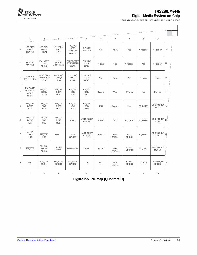
Figure 2-2 through Figure 2-5 show the bottom view of the package pin assignments in four quadrants (A,B, C, and D).
Figure 2-2. Pin Map [Quadrant A]
Device Overview22 Submit Documentation Feedback

www.ti.com
W
V
U
T
R
P
N
M
L
K
191817161514131211
191817161514131211
DDR_A[9]
VSS
VSSCVDD
CVDD
VSS CVDD
VSSDVDDR2 DVDDR2
DVDDR2VSS
DVDDR2 DVDDR2VSS
DDR_VSSDLL
DDR_ZPDDR_ZN
VSS
VSS
VSSDVDD18
DVDD18
HD PCLK
VDDA_1P8V
CI6/CCD14/UART_TXD2
CI7/CCD15/UART_RXD2
DAC_IOUT_B
RSV4DDR_D[29]DDR_D[27]DDR_D[21]DDR_D[18]
DAC_IOUT_A
YI4/CCD4
DAC_RBIAS
DDR_A[3]
DDR_A[4]
DDR_A[0]
VSS
VSS
DDR_DQM[2]
DDR_D[26]
YI7/CCD7
DDR_D[17] DDR_D[22] DDR_D[24] DDR_D[30]
YI0/CCD0
VSSA_1P8V
CI5/CCD13/UART_CTS2
CI1/CCD9
CI4/CCD12/UART_RTS2
DDR_VREF DDR_DQM[3] DDR_D[23] DAC_IOUT_D
YI1/CCD1 YI3/CCD3
DDR_D[20] DDR_DQS[3] DDR_D[31]
YI6/CCD6 VD
DDR_A[7] DDR_A[2] DDR_D[19] DDR_D[28]
DDR_A[6] DDR_D[16]
DAC_IOUT_C
CVDDDSP VSS
CI2/CCD10
YI5/CCD5
DAC_VREF
DVDD18 CI0/CCD8
CI3/CCD11
DVDDR2 VDDA_1P1V
DVDDR2
VSSA_1P1V
YI2/CCD2
DDR_A[1] DDR_DQS[2] DDR_D[25]
VSS
DDR_A[5] W
V
U
T
R
P
N
M
L
K
TMS320DM6446Digital Media System-on-Chip
SPRS283E–DECEMBER 2005–REVISED MARCH 2007
Figure 2-3. Pin Map [Quadrant B]
Submit Documentation Feedback Device Overview 23

www.ti.com
H
G
F
E
D
C
B
A
191817161514131211
191817161514131211
CVDDDSP
YOUT4/R4/AEAW4
GPIOV33_1/TXCLK
GPIOV33_2/COL
GPIOV33_9/RXD2
GPIOV33_8/RXD1
GPIOV33_6/TXD3
GPIOV33_4/TXD1
GPIOV33_12/RXDV
GPIO2/G0
GPIOV33_7/RXD0
GPIOV33_10/RXD3
DVDD33 DVDD33DVDD33
VSS VSSVSS
GPIO1/C_WE
GPIO0/LCD_OE
GPIO4/R0/C_FIELD
GPIOV33_0/TXEN
GPIO6/B1
VSYNC VPBECLK
M24XI
YOUT3/R3/AEAW3
VCLK
YOUT7/R7CLK_OUT1/
TIM_IN/GPIO49
PWM1/R2/GPIO46
M24VDD
CVDDDSP
GPIO38/R1
DVDD18
VSS
USB_R1
COUT5/G2
COUT0/B3/BTSEL0
YOUT6/R6
YOUT2/G7/AEAW2
COUT7/G4
YOUT1/G6/AEAW1
DVDD18USB_
VSSREF
USB_VSSA1P2LD0
USB_DP
COUT2/B5/EM_WIDTH
RSV2
VSS USB_VSS1P8 USB_DM
COUT3/B6/DSP_BT
COUT6/G3
M24XO
GPIOV33_5/TXD2
PWM2/B2/GPIO47
HSYNC
COUT1/B4/BTSEL1
M24VSS
GPIO3/B0/LCD_FIELD
PWM0/GPIO45
YOUT0/G5/AEAW0
GPIO5/G1 YOUT5/R5
CVDD
USB_VDDA1P2LD0
COUT4/B7
VSS DVDD18 USB_VDD1P8
GPIOV33_3/TXD0
H
G
F
E
D
C
B
A
J CVDDDSP VSSUSB_
VSSA3P3DVDD18 USB_ID
USB_VDDA3P3
CVDDDSP VSS USB_VBUS J
TMS320DM6446Digital Media System-on-ChipSPRS283E–DECEMBER 2005–REVISED MARCH 2007
Figure 2-4. Pin Map [Quadrant C]
Device Overview24 Submit Documentation Feedback
www.ti.com
J
H
G
F
E
D
C
B
A
10987654321
10987654321
EM_BA[1]/DA1/
GPIO52
TMS
SPI_EN0/GPIO37
RSV1
EM_CS3
SPI_CLK/GPIO39
SPI_EN1/HDDIR/GPIO42
EM_CS2/HCS
GPIO7
EM_D12/DD12/HD12
EM_D1/DD1/HD1
EM_D5/DD5/HD5
RSV5
EM_D15/DD15/HD15
EM_D3/DD3/HD3
EM_D9/DD9/HD9
EM_D13/DD13/HD13
EM_D6/DD6/HD6
EM_D8/DD8/HD8
EM_WE/(WE)/(IOWR)/DIOW/
HDS2
EM_D11/DD11/HD11
GPIO51/ATA_CS1
EM_R/W/INTRQ/HR/W
EM_D4/DD4/HD4
SCL/GPIO43
TDOSDA/GPIO44
TDI
SD_DATA3GPIOV33_14/
CRS
VSS
SD_DATA2GPIOV33_13/
RXER
SD_DATA1GPIOV33_15/
MDIO
RTCK
VSS
DMACK/UART_TXD1
EM_BA[0]/DA0/HINT
UART_RXD0/GPIO35
EM_D2/DD2/HD2
EM_D10/DD10/HD10
VSS
SD_CMD
GPIO50/ATA_CS0
DVDD18 VSS CVDDDSP
DR/GPIO34
VSS
SD_DATA0
FSR/GPIO32
TRST
VSS DVDD18 VSS VSS
CLKR/GPIO30
GPIOV33_11/RXCLK
DVDD18 VSS CVDDDSP
CLKX/GPIO29
GPIOV33_16/MDCLK
EM_A[2]/(CLE)/
HCNTL0
EM_A[1]/(ALE)/HHWIL
EM_A[0]/DA2/
HCNTL1/GPIO53
VSS CVDDDSP
DVDD33
SPI_DO/GPIO41
TCK
FSX/GPIO31
DX/GPIO33
DVDD18
EM_D7/DD7/HD7
UART_TXD0/GPIO36
EMU1
EMU0
EM_D0/DD0/HD0
DVDD18
EM_WAIT/(RDY/BSY)/
IORDY/HRDY
DVDD18
DVDD18
SD_CLK
EM_OE/(RE)/(IORD)/DIOR/
HDS1
EM_D14/DD14/HD14
CVDDDSP
DMARQ/UART_RXD1
SPI_DI/GPIO40
J
H
G
F
E
D
C
B
A
TMS320DM6446Digital Media System-on-Chip
SPRS283E–DECEMBER 2005–REVISED MARCH 2007
Figure 2-5. Pin Map [Quadrant D]
Submit Documentation Feedback Device Overview 25

www.ti.com
2.7 Terminal Functions
TMS320DM6446Digital Media System-on-ChipSPRS283E–DECEMBER 2005–REVISED MARCH 2007
The terminal functions tables (Table 2-5 through Table 2-30) identify the external signal names, theassociated pin (ball) numbers along with the mechanical package designator, the pin type, whether the pinhas any internal pullup or pulldown resistors, and a functional pin description. For more detailedinformation on device configuration, peripheral selection, multiplexed/shared pin, and see the DeviceConfigurations section of this data manual.
Table 2-5. BOOT Terminal Functions
SIGNALTYPE (1) OTHER (2) (3) DESCRIPTION
NAME NO.
BOOT
These pins are multiplexed between ARM boot mode and the VPBE. Atreset, the boot mode inputs BTSEL0 and BTSEL1 are sampled toCOUT0/ IPD determine the ARM boot configuration. See below for the boot modes setB3/ A16 I/O/Z DVDD18 by these inputs. See the Bootmode section for more details.BTSEL0 After reset, these are video encoder outputs COUT0 and COUT1, orRGB666/888 Blue output data bits 3 and 4 B3/B4.
BTSEL1 BTSEL0 ARM Boot Mode
0 0 ARM ROM Boot (NAND) [default]COUT1/ IPDB4/ B16 I/O/Z 0 1 ARM EMIFA Boot (NOR)DVDD18BTSEL1 1 0 ARM ROM Boot (HPI)
1 1 ARM ROM Boot (UART0)
This pin is multiplexed between EMIFA and the VPBE. At reset, the inputstate is sampled to set the EMIFA data bus width (EM_WIDTH). For anCOUT2/ IPD 8-bit wide EMIFA data bus, EM_WIDTH = 0. For a 16-bit wide EMIFA dataB5/ A17 I/O/Z DVDD18 bus, EM_WIDTH = 1.EM_WIDTH After reset, it is video encoder output COUT2 or RGB666/888 Blue outputdata bit 5 B5.
This pin is multiplexed between DSP boot and the VPBE. At reset, theinput state is sampled to set the DSP boot source DSP_BT. The DSP isCOUT3/ IPD booted by the ARM when DSP_BT=0. The DSP boots from EMIFA whenB6/ B17 I/O/Z DVDD18 DSP_BT=1.DSP_BT After reset, it is video encoder output COUT3 or RGB666/888 Blue databit 6 output B6.
YOUT0/ IPDG5/ D15 I/O/Z DVDD18AEAW0
YOUT1/ IPDG6/ D16 I/O/Z DVDD18AEAW1 These pins are multiplexed between EMIFA and the VPBE. At reset, theYOUT2/ input states of AEAW[4:0] are sampled to set the EMIFA address busIPDG7/ D17 I/O/Z width. See the Peripheral Selection at Device Reset section for details.DVDD18AEAW2 After reset, these are video encoder outputs YOUT[0:4] or RGB666/888
Red and Green data bit outputs G5, G6, G7, R3, and R4.YOUT3/ IPDR3/ D18 I/O/Z DVDD18AEAW3
YOUT4/ IPDR4/ E15 I/O/Z DVDD18AEAW4
(1) I = Input, O = Output, Z = High impedance, S = Supply voltage, GND = Ground, A = Analog signal(2) IPD = Internal pulldown, IPU = Internal pullup. (To pull up a signal to the opposite supply rail, a 1-kΩ resistor should be used.)(3) Specifies the operating I/O supply voltage for each signal
26 Device Overview Submit Documentation Feedback

www.ti.com
TMS320DM6446Digital Media System-on-Chip
SPRS283E–DECEMBER 2005–REVISED MARCH 2007
Table 2-6. Oscillator/PLL Terminal Functions
SIGNALTYPE (1) OTHER (2) DESCRIPTION
NAME NO.
OSCILLATOR, PLL
Crystal input MXI for MX oscillator (system oscillator, typically 27 MHz). If a crystalMXI/CLKIN L1 I DVDD18 input is not used, but instead a physical clock-in source is supplied, this is the
external oscillator clock input.
Crystal output for MX oscillator. If a crystal input is not used, but instead a physicalMXO M1 O DVDD18 clock-in source is supplied, MXO should be left as a No Connect.
1.8-V power supply for MX oscillator. If a crystal input is not used, but instead aMXVDD L5 S (3) physical clock-in source is supplied, MXVDD should still be connected to the 1.8-V
power supply.
Ground for MX oscillator. If a crystal input is not used, but instead a physicalMXVSS L2 GND (3)clock-in source is supplied, MXVSS should still be connected to ground.
Crystal input for M24 oscillator (24 MHz for USB). If a crystal input is not used, butM24XI F18 I DVDD18 instead a physical clock-in source is supplied, this is the external oscillator clock
input. When the USB peripheral is not used, M24XI should be left as a No Connect.
Crystal output for M24 oscillator. If a crystal input is not used, but instead a physicalM24XO F19 O DVDD18 clock-in source is supplied, M24XO should be left as a No Connect. When the USB
peripheral is not used, M24XO should be left as a No Connect.
1.8-V power supply for M24 oscillator. If a crystal input is not used, but instead aphysical clock-in source is supplied, M24VDD should still be connected to the 1.8-VM24VDD F16 S (3)power supply. When the USB peripheral is not used, M24VDD should be connectedto the 1.8-V power supply.
Ground for M24 oscillator. If a crystal input is not used, but instead a physicalM24VSS F17 GND (3) clock-in source is supplied, M24VSS should still be connected to ground. When the
USB peripheral is not used, M24VSS should be connected to ground.
PLLVDD18 M2 S (3) 1.8-V power supply for PLLs (system).
(1) I = Input, O = Output, Z = High impedance, S = Supply voltage, GND = Ground, A = Analog signal(2) Specifies the operating I/O supply voltage for each signal(3) For more information, see the Recommended Operating Conditions table
Table 2-7. Clock Generator Terminal Functions
SIGNALTYPE (1) OTHER (2) DESCRIPTION
NAME NO.
CLOCK GENERATOR
This pin is multiplexed between the PLL1 clock generator and GPIO.CLK_OUT0/ K1 I/O/Z DVDD18 For the PLL1 clock generator, it is clock output CLK_OUT0. This is configurable forGPIO48 13.5 MHz or 27 MHz clock outputs.
CLK_OUT1/ This pin is multiplexed between the USB clock generator, timer, and GPIO.TIM_IN/ E19 I/O/Z DVDD18 For the USB clock generator, it is clock output CLK_OUT1. This is configurable forGPIO49 12 MHz or 24 MHz clock outputs.
(1) I = Input, O = Output, Z = High impedance, S = Supply voltage, GND = Ground, A = Analog signal(2) Specifies the operating I/O supply voltage for each signal
Table 2-8. RESET and JTAG Terminal Functions
SIGNALTYPE (1) OTHER (2) (3) DESCRIPTION
NAME NO.
RESET
IPURESET L4 I This is the active low global reset input.DVDD18
JTAG
(1) I = Input, O = Output, Z = High impedance, S = Supply voltage, GND = Ground, A = Analog signal(2) IPD = Internal pulldown, IPU = Internal pullup. (To pull up a signal to the opposite supply rail, a 1-kΩ resistor should be used.)(3) Specifies the operating I/O supply voltage for each signal
Submit Documentation Feedback Device Overview 27

www.ti.com
TMS320DM6446Digital Media System-on-ChipSPRS283E–DECEMBER 2005–REVISED MARCH 2007
Table 2-8. RESET and JTAG Terminal Functions (continued)
SIGNALTYPE (1) OTHER (2) (3) DESCRIPTION
NAME NO.
IPUTMS E6 I JTAG test-port mode select inputDVDD18
–TDO B5 O/Z JTAG test-port data outputDVDD18
IPUTDI A5 I JTAG test-port data inputDVDD18
IPUTCK A6 I JTAG test-port clock inputDVDD18
–RTCK B6 O/Z JTAG test-port return clock outputDVDD18
IPD JTAG test-port reset. For IEEE 1149.1 JTAG compatibility, see the IEEE 1149.1TRST D7 I DVDD18 JTAG compatibility statement portion of this data manual .
IPUEMU1 C6 I/O/Z Emulation pin 1DVDD18
IPUEMU0 D6 I/O/Z Emulation pin 0DVDD18
Table 2-9. EMIFA Terminal Functions
SIGNALTYPE (1) OTHER (2) (3) DESCRIPTION
NAME NO.
EMIFA BOOT CONFIGURATION
This pin is multiplexed between EMIFA and the VPBE. At reset, the input state isCOUT2/ sampled to set the EMIFA data bus width (EM_WIDTH). For an 8-bit wide EMIFAIPDB5/ A17 I/O/Z data bus, EM_WIDTH = 0. For a 16-bit wide EMIFA data bus, EM_WIDTH = 1.DVDD18EM_WIDTH After reset, it is video encoder output COUT2 or RGB666/888 Blue output data bit 5
B5.
This pin is multiplexed between DSP boot and the VPBE. At reset, the input state isCOUT3/ sampled to set the DSP boot source DSP_BT. The DSP is booted by the ARM whenIPDB6/ B17 I/O/Z DSP_BT=0. The DSP boots from EMIFA when DSP_BT=1.DVDD18DSP_BT After reset, it is video encoder output COUT3 or RGB666/888 Blue data bit 6 output
B6.
YOUT0/ IPDG5/ D15 I/O/Z DVDD18AEAW0
YOUT1/ IPDG6/ D16 I/O/Z DVDD18AEAW1 These pins are multiplexed between EMIFA and the VPBE. At reset, the input statesYOUT2/ of AEAW[4:0] are sampled to set the EMIFA address bus width. See the PeripheralIPDG7/ D17 I/O/Z Selection at Device Reset section for details.DVDD18AEAW2 After reset, these are video encoder outputs YOUT[0:4] or RGB666/888 Red and
Green data bit outputs G5, G6, G7, R3, and R4.YOUT3/ IPDR3/ D18 I/O/Z DVDD18AEAW3
YOUT4/ IPDR4/ E15 I/O/Z DVDD18AEAW4
EMIFA FUNCTIONAL PINS: ASYNC / NOR
This pin is multiplexed between EMIFA and HPI.EM_CS2/ For EMIFA, this pin is Chip Select 2 output EM_CS2 for use with asynchronousC2 I/O/Z DVDD18HCS memories (i.e., NOR flash) or NAND flash. This is the chip select for the default boot
and ROM boot modes.
For EMIFA, this pin is Chip Select 3 output EM_CS3 for use with asynchronousEM_CS3 B1 I/O/Z DVDD18 memories (i.e., NOR flash) or NAND flash.
(1) I = Input, O = Output, Z = High impedance, S = Supply voltage, GND = Ground, A = Analog signal(2) IPD = Internal pulldown, IPU = Internal pullup. (To pull up a signal to the opposite supply rail, a 1-kΩ resistor should be used.)(3) Specifies the operating I/O supply voltage for each signal
Device Overview28 Submit Documentation Feedback

www.ti.com
TMS320DM6446Digital Media System-on-Chip
SPRS283E–DECEMBER 2005–REVISED MARCH 2007
Table 2-9. EMIFA Terminal Functions (continued)
SIGNALTYPE (1) OTHER (2) (3) DESCRIPTION
NAME NO.
EM_CS4/ This pin is multiplexed between EMIFA, GPIO, and VLYNQ.GPIO9/ T2 I/O/Z DVDD18 For EMIFA, it is Chip Select 4 output EM_CS4 for use with asynchronous memories
VLYNQ_SCRUN (i.e., NOR flash) or NAND flash.
EM_CS5/ This pin is multiplexed between EMIFA, GPIO, and VLYNQ.GPIO8/ T1 I/O/Z DVDD18 For EMIFA, it is Chip Select 5 output EM_CS5 for use with asynchronous memories
VLYNQ_CLOCK (i.e., NOR flash) or NAND flash.
EM_R/W/ This pin is multiplexed between EMIFA, ATA/CF, and HPI.INTRQ/ G3 I/O/Z DVDD18 For EMIFA, it is read/write output EM_R/W.HR/W
EM_WAIT/(RDY/BSY)/ IPU This pin is multiplexed between EMIFA (NAND/SmartMedia/xD), ATA/CF, and HPI.F1 I/O/ZIORDY/ DVDD18 For EMIFA, it is wait state extension input EM_WAIT.
HRDY
EM_OE/(RE)/ This pin is multiplexed between EMIFA (NAND/SmartMedia/xD), ATA/CF, and HPI.(IORD)/ H4 I/O/Z DVDD18 For EMIFA, it is output enable output EM_OE.DIOR/HDS1
EM_WE(WE) This pin is multiplexed between EMIFA (NAND/SmartMedia/xD), ATA/CF, and HPI.(IOWR)/ G2 I/O/Z DVDD18 For NAND/SmartMedia/xD or EMIFA, it is write enable output EM_WE.DIOW/HDS2
This pin is multiplexed between EMIFA, ATA/CF, and HPI.For EMIFA, this is the Bank Address 0 output (EM_BA[0]).EM_BA[0]/ IPD When connected to an 8-bit asynchronous memory, this pin is the lowest order bit ofDA0/ J3 I/O/Z DVDD18 the byte address.HINT When connected to a 16-bit asynchronous memory, this pin has the same functionas EMIF address pin 22 (EM_A[22]).
This pin is multiplexed between EMIFA, ATA/CF, and GPIO.For EMIFA, this is the Bank Address 1 output EM_BA[1].EM_BA[1]/ When connected to a 16 bit asynchronous memory this pin is the lowest order bit ofDA1/ H2 I/O/Z DVDD18 the 16-bit word address.GPIO52 When connected to an 8-bit asynchronous memory, this pin is the 2nd bit of theaddress.
EM_A[21]/ This pin is multiplexed between EMIFA, GPIO, and VLYNQ.GPIO10/ T3 I/O/Z DVDD18 For EMIFA, it is address bit 21 output EM_A[21].VLYNQ_TXD0
EM_A[20]/ This pin is multiplexed between EMIFA, GPIO, and VLYNQ.GPIO11/ R3 I/O/Z DVDD18 For EMIFA, it is address bit 20 output EM_A[20].VLYNQ_RXD0
EM_A[19]/ This pin is multiplexed between EMIFA, GPIO, and VLYNQ.GPIO12/ R4 I/O/Z DVDD18 For EMIFA, it is address bit 19 output EM_A[19].VLYNQ_TXD1
EM_A[18]/ This pin is multiplexed between EMIFA, GPIO, and VLYNQ.GPIO13/ P5 I/O/Z DVDD18 For EMIFA, it is address bit 18 output EM_A[18].VLYNQ_RXD1
EM_A[17]/ This pin is multiplexed between EMIFA, GPIO, and VLYNQ.GPIO14/ R2 I/O/Z DVDD18 For EMIFA, it is address bit 17 output EM_A[17].VLYNQ_TXD2
EM_A[16]/ This pin is multiplexed between EMIFA, GPIO, and VLYNQ.GPIO15/ R5 I/O/Z DVDD18 For EMIFA, it is address bit 16 output EM_A[16].VLYNQ_RXD2
EM_A[15]/ This pin is multiplexed between EMIFA, GPIO, and VLYNQ.GPIO16/ P3 I/O/Z DVDD18 For EMIFA, it is address bit 15 output EM_A[15].VLYNQ_TXD3
EM_A[14]/ This pin is multiplexed between EMIFA, GPIO, and VLYNQ.GPIO17/ P4 I/O/Z DVDD18 For EMIFA, it is address bit 14 output EM_A[14].VLYNQ_RXD3
Submit Documentation Feedback Device Overview 29

www.ti.com
TMS320DM6446Digital Media System-on-ChipSPRS283E–DECEMBER 2005–REVISED MARCH 2007
Table 2-9. EMIFA Terminal Functions (continued)
SIGNALTYPE (1) OTHER (2) (3) DESCRIPTION
NAME NO.
EM_A[13]/ This pin is multiplexed between EMIFA and GPIO.N4 I/O/Z DVDD18GPIO18 For EMIFA, it is address bit 13 output EM_A[13].
EM_A[12]/ This pin is multiplexed between EMIFA and GPIO.R1 I/O/Z DVDD18GPIO19 For EMIFA, it is address bit 12 output EM_A[12].
EM_A[11]/ This pin is multiplexed between EMIFA and GPIO.P2 I/O/Z DVDD18GPIO20 For EMIFA, it is address bit 11 output EM_A[11].
EM_A[10]/ This pin is multiplexed between EMIFA and GPIO.P1 I/O/Z DVDD18GPIO21 For EMIFA, it is address bit 10 output EM_A[10].
EM_A[9]/ This pin is multiplexed between EMIFA and GPIO.M4 I/O/Z DVDD18GPIO22 For EMIFA, it is address bit 9 output EM_A[9].
EM_A[8]/ This pin is multiplexed between EMIFA and GPIO.N3 I/O/Z DVDD18GPIO23 For EMIFA, it is address bit 8 output EM_A[8].
EM_A[7]/ This pin is multiplexed between EMIFA and GPIO.N2 I/O/Z DVDD18GPIO24 For EMIFA, it is address bit 7 output EM_A[7].
EM_A[6]/ This pin is multiplexed between EMIFA and GPIO.N1 I/O/Z DVDD18GPIO25 For EMIFA, it is address bit 6 output EM_A[6].
EM_A[5]/ This pin is multiplexed between EMIFA and GPIO.K3 I/O/Z DVDD18GPIO26 For EMIFA, it is address bit 5 output EM_A[5].
EM_A[4]/ This pin is multiplexed between EMIFA and GPIO.K4 I/O/Z DVDD18GPIO27 For EMIFA, it is address bit 4 output EM_A[4].
EM_A[3]/ This pin is multiplexed between EMIFA and GPIO.K2 I/O/Z DVDD18GPIO28 For EMIFA, it is address bit 3 output EM_A[3].
EM_A[2]/ This pin is multiplexed between EMIFA and HPI.(CLE)/ J1 I/O/Z DVDD18 For EMIFA, this pin is the EM_A[2] address line.HCNTL0
EM_A[1]/(ALE)/ J2 I/O/Z DVDD18 This pin is multiplexed between EMIFA (NAND/SmartMedia.xD) and HPI.HHWIL
This pin is multiplexed between EMIFA, ATA/CF, HPI, and GPIO.EM_A[0]/ For EMIFA, this is Address output EM_A[0], which is the least significant bit on a
DA2/ 32-bit word address.J4 I/O/Z DVDD18HCNTL1/ When connected to a 16-bit asynchronous memory, this pin is the 2nd bit of theGPIO53 address.
For an 8-bit asynchronous memory, this pin is the 3rd bit of the address.
Device Overview30 Submit Documentation Feedback

www.ti.com
TMS320DM6446Digital Media System-on-Chip
SPRS283E–DECEMBER 2005–REVISED MARCH 2007
Table 2-9. EMIFA Terminal Functions (continued)
SIGNALTYPE (1) OTHER (2) (3) DESCRIPTION
NAME NO.
EM_D0/DD0/ E5 I/O/Z DVDD18HD0
EM_D1/DD1/ D3 I/O/Z DVDD18HD1
EM_D2/DD2/ F5 I/O/Z DVDD18HD2
EM_D3/DD3/ E3 I/O/Z DVDD18HD3
EM_D4/DD4/ E4 I/O/Z DVDD18HD4
EM_D5/DD5/ D2 I/O/Z DVDD18HD5
EM_D6/DD6/ F4 I/O/Z DVDD18HD6
EM_D7/DD7/ C1 I/O/Z DVDD18
These pins are multiplexed between EMIFA (NAND), ATA/CF, and HPI. In all casesHD7they are used as a 16 bit bi-directional data bus.
EM_D8/ For EMIFA (NAND), these are EM_D[15:0].DD8/ F3 I/O/Z DVDD18HD8
EM_D9/DD9/ E2 I/O/Z DVDD18HD9
EM_D10/DD10/ G5 I/O/Z DVDD18HD10
EM_D11/DD11/ G4 I/O/Z DVDD18HD11
EM_D12/DD12/ D1 I/O/Z DVDD18HD12
EM_D13/DD13/ F2 I/O/Z DVDD18HD13
EM_D14/DD14/ H5 I/O/Z DVDD18HD14
EM_D15/DD15/ E1 I/O/Z DVDD18HD15
Submit Documentation Feedback Device Overview 31

www.ti.com
TMS320DM6446Digital Media System-on-ChipSPRS283E–DECEMBER 2005–REVISED MARCH 2007
Table 2-9. EMIFA Terminal Functions (continued)
SIGNALTYPE (1) OTHER (2) (3) DESCRIPTION
NAME NO.
EMIFA FUNCTIONAL PINS: NAND / SMARTMEDIA / xD
EM_A[1]/ This pin is multiplexed between EMIFA and HPI.(ALE)/ J2 I/O/Z DVDD18 For NAND/SmartMedia/xD, it is Address Latch Enable output (ALE).HHWIL
EM_A[2]/ This pin is multiplexed between EMIFA and HPI.(CLE)/ J1 I/O/Z DVDD18 For NAND/SmartMedia/xD, this pin is the Command Latch Enable output (CLE).HCNTL0
EM_WAIT/(RDY/BSY)/ IPU This pin is multiplexed between EMIFA (NAND/SmartMedia/xD), ATA/CF, and HPI.F1 I/O/ZIORDY/ DVDD18 For NAND/SmartMedia/xD, it is ready/busy input (RDY/BSY).
HRDY
EM_OE/(RE)/ This pin is multiplexed between EMIFA (NAND/SmartMedia/xD), ATA/CF, and HPI.(IORD)/ H4 I/O/Z DVDD18 For NAND/SmartMedia/xD, it is read enable output (RE).DIOR/HDS1
EM_WE(WE) This pin is multiplexed between EMIFA (NAND/SmartMedia/xD), ATA/CF, and HPI.(IOWR)/ G2 I/O/Z DVDD18 For NAND/SmartMedia/xD, it is write enable output (WE).DIOW/HDS2
This pin is multiplexed between EMIFA and HPI.EM_CS2/ For EMIFA, this pin is Chip Select 2 output EM_CS2 for use with asynchronousC2 I/O/Z DVDD18HCS memories (i.e. NOR flash) or NAND flash. This is the chip select for the default boot
and ROM boot modes.
For EMIFA, this pin is Chip Select 3 output EM_CS3 for use with asynchronousEM_CS3 B1 I/O/Z DVDD18 memories (i.e. NOR flash) or NAND flash.
EM_CS4/ This pin is multiplexed between EMIFA, GPIO, and VLYNQ. For EMIFA, it is ChipGPIO9/ T2 I/O/Z DVDD18 Select 4 output EM_CS4 for use with asynchronous memories (i.e., NOR flash) or
VLYNQ_SCRUN NAND flash.
EM_CS5/ This pin is multiplexed between EMIFA, GPIO, and VLYNQ. For EMIFA, it is ChipGPIO8/ T1 I/O/Z DVDD18 Select 5 output EM_CS5 for use with asynchronous memories (i.e., NOR flash) or
VLYNQ_CLOCK NAND flash.
Device Overview32 Submit Documentation Feedback

www.ti.com
TMS320DM6446Digital Media System-on-Chip
SPRS283E–DECEMBER 2005–REVISED MARCH 2007
Table 2-9. EMIFA Terminal Functions (continued)
SIGNALTYPE (1) OTHER (2) (3) DESCRIPTION
NAME NO.
EM_D0/DD0/ E5 I/O/Z DVDD18HD0
EM_D1/DD1/ D3 I/O/Z DVDD18HD1
EM_D2/DD2/ F5 I/O/Z DVDD18HD2
EM_D3/DD3/ E3 I/O/Z DVDD18HD3
EM_D4/DD4/ E4 I/O/Z DVDD18HD4
EM_D5/DD5/ D2 I/O/Z DVDD18HD5
EM_D6/DD6/ F4 I/O/Z DVDD18HD6
EM_D7/DD7/ C1 I/O/Z DVDD18
These pins are multiplexed between EMIFA (NAND), ATA/CF, and HPI. In all casesHD7they are used as a 16 bit bi-directional data bus.
EM_D8/ For EMIFA (NAND), these are EM_D[15:0].DD8/ F3 I/O/Z DVDD18HD8
EM_D9/DD9/ E2 I/O/Z DVDD18HD9
EM_D10/DD10/ G5 I/O/Z DVDD18HD10
EM_D11/DD11/ G4 I/O/Z DVDD18HD11
EM_D12/DD12/ D1 I/O/Z DVDD18HD12
EM_D13/DD13/ F2 I/O/Z DVDD18HD13
EM_D14/DD14/ H5 I/O/Z DVDD18HD14
EM_D15/DD15/ E1 I/O/Z DVDD18HD15
Submit Documentation Feedback Device Overview 33

www.ti.com
TMS320DM6446Digital Media System-on-ChipSPRS283E–DECEMBER 2005–REVISED MARCH 2007
Table 2-10. DDR2 Memory Controller Terminal Functions
SIGNALTYPE (1) OTHER (2) (3) DESCRIPTION
NAME NO.
DDR2 Memory Controller
DDR_CLK0 W7 I/O/Z DVDDR2 DDR2 Clock
DDR_CLK0 W8 I/O/Z DVDDR2 DDR2 Differential clock
DDR_CKE V8 I/O/Z DVDDR2 DDR2 Clock Enable
DDR_CS T9 I/O/Z DVDDR2 DDR2 Active low chip select
DDR_WE T8 I/O/Z DVDDR2 DDR2 Active low Write enable
DDR_DQM[3] T16 I/O/Z DVDDR2 DDR2 Data mask outputsDQM3: For upper byte data bus DDR_D[31:24]DDR_DQM[2] T14 I/O/Z DVDDR2DQM2: For DDR_D[23:16]
DDR_DQM[1] T6 I/O/Z DVDDR2 DQM1: For DDR_D[15:8]DQM0: For lower byte DDR_D[7:0]DDR_DQM[0] T4 I/O/Z DVDDR2
DDR_RAS U7 I/O/Z DVDDR2 DDR2 Row Access Signal output
DDR_CAS T7 I/O/Z DVDDR2 DDR2 Column Access Signal output
DDR_DQS[0] U4 I/O/Z DVDDR2 Data strobe input/outputs for each byte of the 32-bit data bus. They are outputs tothe DDR2 memory when writing and inputs when reading. They are used toDDR_DQS[1] U6 I/O/Z DVDDR2 synchronize the data transfers.
DDR_DQS[2] U14 I/O/Z DVDDR2 DQS3 : For upper byte DDR_D[31:24]DQS2: For DDR_D[23:16]DQS1: For DDR_D[15:8]DDR_DQS[3] U16 I/O/Z DVDDR2DQS0: For bottom byte DDR_D[7:0]
DDR_BS[0] U8
DDR_BS[1] V9 I/O/Z DVDDR2 Bank select outputs (BS[2:0]). Two are required to support 1Gb DDR2 memories.
DDR_BS[2] U9
DDR_A[12] W9
DDR_A[11] W10
DDR_A[10] U10
DDR_A[9] U11
DDR_A[8] V10
DDR_A[7] V11
DDR_A[6] W11 I/O/Z DVDDR2 DDR2 address bus
DDR_A[5] W12
DDR_A[4] V12
DDR_A[3] U12
DDR_A[2] V13
DDR_A[1] U13
DDR_A[0] W13
(1) I = Input, O = Output, Z = High impedance, S = Supply voltage, GND = Ground, A = Analog signal(2) Specifies the operating I/O supply voltage for each signal(3) For more information, see the Recommended Operating Conditions table
Device Overview34 Submit Documentation Feedback

www.ti.com
TMS320DM6446Digital Media System-on-Chip
SPRS283E–DECEMBER 2005–REVISED MARCH 2007
Table 2-10. DDR2 Memory Controller Terminal Functions (continued)
SIGNALTYPE (1) OTHER (2) (3) DESCRIPTION
NAME NO.
DDR_D[31] U19
DDR_D[30] V19
DDR_D[29] W18
DDR_D[28] V18
DDR_D[27] W17
DDR_D[26] U18
DDR_D[25] U17
DDR_D[24] V17
DDR_D[23] T17
DDR_D[22] V16
DDR_D[21] W16
DDR_D[20] U15
DDR_D[19] V15
DDR_D[18] W15
DDR_D[17] V14
DDR_D[16] W14I/O/Z DVDDR2 DDR2 data bus can be configured as 32 bits wide or 16 bits wide.
DDR_D[15] V7
DDR_D[14] W6
DDR_D[13] V6
DDR_D[12] W5
DDR_D[11] V5
DDR_D[10] U5
DDR_D[9] W4
DDR_D[8] V4
DDR_D[7] W3
DDR_D[6] V3
DDR_D[5] U3
DDR_D[4] W2
DDR_D[3] V2
DDR_D[2] V1
DDR_D[1] U2
DDR_D[0] U1
DDR_VREF T15 I (3) Reference voltage input for the SSTL_18 IO buffers.
DDR_VSSDLL T11 GND (3) Ground for the DDR2 Digital Locked Loop.
DDR_VDDDLL T10 S (3) Power (1.8 Volts) for the DDR2 Digital Locked Loop.
Impedance control for DDR2 outputs. This must be connected via a 200 Ω resistorDDR_ZN T12 O/Z (3)to DVDDR2.
Impedance control for DDR2 outputs. This must be connected via a 200 Ω resistorDDR_ZP T13 O/Z (3)to VSS.
Submit Documentation Feedback Device Overview 35

www.ti.com
TMS320DM6446Digital Media System-on-ChipSPRS283E–DECEMBER 2005–REVISED MARCH 2007
Table 2-11. I2C Terminal Functions
SIGNALTYPE (1) OTHER (2) DESCRIPTION
NAME NO.
I2C
SCL/ This pin is multiplexed between I2C and GPIO.C4 I/O/Z DVDD18GPIO43 For I2C, it is clock output SCL.
SDA/ This pin is multiplexed between I2C and GPIO.B4 I/O/Z DVDD18GPIO44 For I2C, it is bi-directional data signal SDA.
(1) I = Input, O = Output, Z = High impedance, S = Supply voltage, GND = Ground, A = Analog signal(2) Specifies the operating I/O supply voltage for each signal
Table 2-12. Audio Serial Port (ASP) Terminal Functions
SIGNALTYPE (1) OTHER (2) DESCRIPTION
NAME NO.
Audio Serial Port (ASP)
CLKX/ This pin is multiplexed between ASP and GPIO.B8 I/O/Z DVDD18GPIO29 For ASP, it is Transmit clock IO CLKX.
CLKR/ This pin is multiplexed between ASP and GPIO.A8 I/O/Z DVDD18GPIO30 For ASP, it is Receive clock IO CLKR.
FSX/ This pin is multiplexed between ASP and GPIO.C8 I/O/Z DVDD18GPIO31 For ASP, it is Transmit frame synchronization IO FSX.
FSR/ This pin is multiplexed between ASP and GPIO.C7 I/O/Z DVDD18GPIO32 For ASP, it is Receive frame synchronization IO FSR.
DX/ This pin is multiplexed between ASP and GPIO.B7 I/O/Z DVDD18GPIO33 For ASP, it is Data Transmit output DX.
DR/ This pin is multiplexed between ASP and GPIO.A7 I/O/Z DVDD18GPIO34 For ASP, it is Data Receive input DR.
(1) I = Input, O = Output, Z = High impedance, S = Supply voltage, GND = Ground, A = Analog signal(2) Specifies the operating I/O supply voltage for each signal
Table 2-13. SPI Terminal Functions
SIGNALTYPE (1) OTHER (2) DESCRIPTION
NAME NO.
Serial Port Interface (SPI)
SPI_EN0/ This pin is multiplexed between SPI and GPIO.A4 I/O/Z DVDD18GPIO37 When used by SPI, it is SPI slave device 0 enable output SPI_EN0.
SPI_EN1/ This pin is multiplexed between SPI, ATA, and GPIO.HDDIR/ B2 I/O/Z DVDD18 When used by SPI, it is SPI slave device 1 enable output SPI_EN1.GPIO42
SPI_CLK/ This pin is multiplexed between SPI and GPIO.A3 I/O/Z DVDD18GPIO39 For SPI, it is clock output SPI_CLK.
SPI_DI/ This pin is multiplexed between SPI and GPIO.B3 I/O/Z DVDD18GPIO40 For SPI, it is data input SPI_DI.
SPI_DO/ This pin is multiplexed between SPI and GPIO.A2 I/O/Z DVDD18GPIO41 For SPI it is data output SPI_DO.
(1) I = Input, O = Output, Z = High impedance, S = Supply voltage, GND = Ground, A = Analog signal(2) Specifies the operating I/O supply voltage for each signal
Device Overview36 Submit Documentation Feedback

www.ti.com
TMS320DM6446Digital Media System-on-Chip
SPRS283E–DECEMBER 2005–REVISED MARCH 2007
Table 2-14. EMAC and MDIO Terminal Functions
SIGNALTYPE (1) OTHER (2) DESCRIPTION
NAME NO.
EMAC
GPIOV33_0/ This pin is multiplexed between GPIO and Ethernet MAC.B13 I/O/Z DVDD33TXEN In Ethernet MAC mode, it is Transmit Enable output TXEN.
GPIOV33_1/ This pin is multiplexed between GPIO and Ethernet MAC.A13 I/O/Z DVDD33TXCLK In Ethernet MAC mode, it is Transmit Clock input TXCLK.
GPIOV33_2/ This pin is multiplexed between GPIO and Ethernet MAC.A12 I/O/Z DVDD33COL In Ethernet MAC mode, it is Collision Detect input COL.
GPIOV33_6/ This pin is multiplexed between GPIO and Ethernet MAC.C12 I/O/Z DVDD33TXD3 In Ethernet MAC mode, it is Transmit Data 3 output TXD3.
GPIOV33_5/ This pin is multiplexed between GPIO and Ethernet MAC.A11 I/O/Z DVDD33TXD2 In Ethernet MAC mode, it is Transmit Data 2 output TXD2.
GPIOV33_4/ This pin is multiplexed between GPIO and Ethernet MAC.D12 I/O/Z DVDD33TXD1 In Ethernet MAC mode, it is Transmit Data 1 output TXD1.
GPIOV33_3/ This pin is multiplexed between GPIO and Ethernet MAC.B12 I/O/Z DVDD33TXD0 In Ethernet MAC mode, it is Transmit Data 0 output TXD0.
GPIOV33_11/ This pin is multiplexed between GPIO and Ethernet MAC.A10 I/O/Z DVDD33RXCLK In Ethernet MAC mode, it is Receive Clock input RXCLK.
GPIOV33_12/ This pin is multiplexed between GPIO and Ethernet MAC.D11 I/O/Z DVDD33RXDV In Ethernet MAC mode, it is Receive Data Valid input RXDV.
GPIOV33_13/ This pin is multiplexed between GPIO and Ethernet MAC.D10 I/O/Z DVDD33RXER In Ethernet MAC mode, it is Receive Error input RXER.
GPIOV33_14/ This pin is multiplexed between GPIO and Ethernet MAC.C10 I/O/Z DVDD33CRS In Ethernet MAC mode, it is Carrier Sense input CRS.
GPIOV33_10/ This pin is multiplexed between GPIO and Ethernet MAC.E11 I/O/Z DVDD33RXD3 In Ethernet MAC mode, it is Receive Data 3 input RXD3.
GPIOV33_9/ This pin is multiplexed between GPIO and Ethernet MAC.B11 I/O/Z DVDD33RXD2 In Ethernet MAC mode, it is Receive Data 2 input RXD2.
GPIOV33_8/ This pin is multiplexed between GPIO and Ethernet MAC.C11 I/O/Z DVDD33RXD1 In Ethernet MAC mode, it is Receive data 1 input RXD1.
GPIOV33_7/ This pin is multiplexed between GPIO and Ethernet MAC.E12 I/O/Z DVDD33RXD0 In Ethernet MAC mode, it is Receive Data 0 input RXD0.
MDIO
GPIOV33_16/ This pin is multiplexed between GPIO and Ethernet MAC.B10 I/O/Z DVDD33MDCLK In Ethernet MAC mode, it is Management Data Clock output MDCLK.
GPIOV33_15/ This pin is multiplexed between GPIO and Ethernet MAC.E10 I/O/Z DVDD33MDIO In Ethernet MAC mode, it is Management Data IO MDIO.
(1) I = Input, O = Output, Z = High impedance, S = Supply voltage, GND = Ground, A = Analog signal(2) Specifies the operating I/O supply voltage for each signal
Table 2-15. GPIOV33 Terminal Functions
SIGNALTYPE (1) OTHER (2) DESCRIPTION
NAME NO.
GPIOV33
GPIOV33_16/ This pin is multiplexed between GPIO and Ethernet MAC.B10 I/O/Z DVDD33MDCLK In GPIO mode, it is 3.3V GPIO GPIOV33_16.
GPIOV33_15/ This pin is multiplexed between GPIO and Ethernet MAC.E10 I/O/Z DVDD33MDIO In GPIO mode, it is 3.3V GPIO GPIOV33_15.
GPIOV33_14/ This pin is multiplexed between GPIO and Ethernet MAC.C10 I/O/Z DVDD33CRS In GPIO mode, it is 3.3V GPIO GPIOV33_14.
(1) I = Input, O = Output, Z = High impedance, S = Supply voltage, GND = Ground, A = Analog signal(2) Specifies the operating I/O supply voltage for each signal
Submit Documentation Feedback Device Overview 37

www.ti.com
TMS320DM6446Digital Media System-on-ChipSPRS283E–DECEMBER 2005–REVISED MARCH 2007
Table 2-15. GPIOV33 Terminal Functions (continued)
SIGNALTYPE (1) OTHER (2) DESCRIPTION
NAME NO.
GPIOV33_13/ This pin is multiplexed between GPIO and Ethernet MAC.D10 I/O/Z DVDD33RXER In GPIO mode, it is 3.3V GPIO GPIOV33_13.
GPIOV33_12/ This pin is multiplexed between GPIO and Ethernet MAC.D11 I/O/Z DVDD33RXDV In GPIO mode, it is 3.3V GPIO GPIOV33_12.
GPIOV33_11/ This pin is multiplexed between GPIO and Ethernet MAC.A10 I/O/Z DVDD33RXCLK In GPIO mode, it is 3.3V GPIO GPIOV33_11.
GPIOV33_10/ This pin is multiplexed between GPIO and Ethernet MAC.E11 I/O/Z DVDD33RXD3 In GPIO mode, it is 3.3V GPIO GPIOV33_10.
GPIOV33_9/ This pin is multiplexed between GPIO and Ethernet MAC.B11 I/O/Z DVDD33RXD2 In GPIO mode, it is 3.3V GPIO GPIOV33_9.
GPIOV33_8/ This pin is multiplexed between GPIO and Ethernet MAC.C11 I/O/Z DVDD33RXD1 In GPIO mode, it is 3.3V GPIO GPIOV33_8.
GPIOV33_7/ This pin is multiplexed between GPIO and Ethernet MAC.E12 I/O/Z DVDD33RXD0 In GPIO mode, it is 3.3V GPIO GPIOV33_7.
GPIOV33_6/ This pin is multiplexed between GPIO and Ethernet MAC.C12 I/O/Z DVDD33TXD3 In GPIO mode, it is 3.3V GPIO GPIOV33_6.
GPIOV33_5/ This pin is multiplexed between GPIO and Ethernet MAC.A11 I/O/Z DVDD33TXD2 In GPIO mode, it is 3.3V GPIO GPIOV33_5.
GPIOV33_4/ This pin is multiplexed between GPIO and Ethernet MAC.D12 I/O/Z DVDD33TXD1 In GPIO mode, it is 3.3V GPIO GPIOV33_4.
GPIOV33_3/ This pin is multiplexed between GPIO and Ethernet MAC.B12 I/O/Z DVDD33TXD0 In GPIO mode, it is 3.3V GPIO GPIOV33_3.
GPIOV33_2/ This pin is multiplexed between GPIO and Ethernet MAC.A12 I/O/Z DVDD33COL In GPIO mode, it is 3.3V GPIO GPIOV33_2.
GPIOV33_1/ This pin is multiplexed between GPIO and Ethernet MAC.A13 I/O/Z DVDD33TXCLK In GPIO mode, it is 3.3V GPIO GPIOV33_1.
GPIOV33_0/ This pin is multiplexed between GPIO and Ethernet MAC.B13 I/O/Z DVDD33TXEN In GPIO mode, this pin is 3.3V GPIO pin GPIOV33_0.
Table 2-16. Standalone GPIOV18 Terminal Functions
SIGNALTYPE (1) OTHER (2) DESCRIPTION
NAME NO.
Standalone GPIOV18
GPIO7 C3 I/O/Z DVDD18 This pin is standalone and functions as GPIO7.
(1) I = Input, O = Output, Z = High impedance, S = Supply voltage, GND = Ground, A = Analog signal(2) Specifies the operating I/O supply voltage for each signal
Device Overview38 Submit Documentation Feedback

www.ti.com
TMS320DM6446Digital Media System-on-Chip
SPRS283E–DECEMBER 2005–REVISED MARCH 2007
Table 2-17. USB Terminal Functions
SIGNALTYPE (1) OTHER (2) (3) DESCRIPTION
NAME NO.
USB 2.0
Crystal input for M24 oscillator (24 MHz for USB).
If a crystal input is not used, but instead a physical clock-in source is supplied, thisM24XI F18 I DVDD18 is the external oscillator clock input.
When the USB peripheral is not used, M24XI should be left as a No Connect.
Crystal output for M24 oscillator.
If a crystal input is not used, but instead a physical clock-in source is supplied,M24XO F19 O DVDD18 M24XO should be left as a No Connect.
When the USB peripheral is not used, M24XO should be left as a No Connect.
1.8-V power supply for M24 oscillator.
If a crystal input is not used, but instead a physical clock-in source is supplied,M24VDD F16 S (3) M24VDD should still be connected to the 1.8-V power supply.
When the USB peripheral is not used, M24VDD should be connected to the 1.8-Vpower supply.
Ground for M24 oscillator.
If a crystal input is not used, but instead a physical clock-in source is supplied,M24VSS F17 GND (3)M24VSS should still be connected to ground.
When the USB peripheral is not used, M24VSS should be connected to ground.
5-V input that signifies that VBUS is connected.
USB_VBUS J17 A I/O (3)When the USB peripheral is not used, the USB_VBUS signal should be eitherpulled down or pulled up via a 10-kΩ resistor.
USB operating mode identification pin. For Host mode operation, pull down this pinto ground (VSS) via an external 1.5-kΩ resistor. For Device mode operation, pull upthis pin to DVDD33 rail via an external 1.5-kΩ resistor.USB_ID J16 A I/O
When the USB peripheral is not used, the USB_ID signal should be either pulleddown or pulled up via a 10-kΩ resistor.
USB_DP G19 A I/O USB bi-directional Data Differential signal pair [positive/negative].
When the USB peripheral is not used, the USB_DP signal should be pulled highUSB_DM H19 A I/Oand the USB_DM signal should be pulled down via a 10-kΩ resistor.
Reference current output. This must be connected via a 10-kΩ ±1% resistor toUSB_VSSREF.
USB_R1 H18 A I/O (3)
When the USB peripheral is not used, the USB_R1 signal should be connected viaa 10-kΩ resistor to USB_VSSREF.
Ground for reference current. This must be connected via a 10-kΩ± 1% resistor toUSB_R1.
USB_VSSREF G16 GND (3)
When the USB peripheral is not used, the USB_VSSREF signal should be connectedto VSS.
Analog 3.3 V power supply for USB phy.
USB_VDDA3P3 J19 S (3)When the USB peripheral is not used, the USB_VDDA3P3 signal should beconnected to DVDD33.
Analog ground for USB phy. When the USB peripheral is not used, theUSB_VSSA3P3 J18 GND (3)USB_VSSA3P3 signal should be connected to VSS.
1.8-V I/O power supply for USB phy.
USB_VDD1P8 H17 S (3)When the USB peripheral is not used, the USB_VDD1P8 signal should be connectedto DVDD18.
(1) I = Input, O = Output, Z = High impedance, S = Supply voltage, GND = Ground, A = Analog signal(2) Specifies the operating I/O supply voltage for each signal(3) For more information, see the Recommended Operating Conditions table
Submit Documentation Feedback Device Overview 39

www.ti.com
TMS320DM6446Digital Media System-on-ChipSPRS283E–DECEMBER 2005–REVISED MARCH 2007
Table 2-17. USB Terminal Functions (continued)
SIGNALTYPE (1) OTHER (2) (3) DESCRIPTION
NAME NO.
I/O Ground for USB phy.
USB_VSS1P8 H16 GND (3)When the USB peripheral is not used, the USB_VSS1P8 signal should be connectedto VSS.
Core Power supply LDO output for USB phy. This must be connected via a 1-µFcapacitor to VSS.
USB_VDDA1P2LDO G18 S (3)
When the USB peripheral is not used, the USB_VDDA1P2LDO signal should still beconnected via a 1-µF capacitor to VSS.
Core Ground for USB phy. This is the ground for the LDO and must be connected toVSS.
USB_VSSA1P2LDO G17 GND (3)
When the USB peripheral is not used, the USB_VSSA1P2LDO signal should still beconnected to VSS.
Device Overview40 Submit Documentation Feedback

www.ti.com
TMS320DM6446Digital Media System-on-Chip
SPRS283E–DECEMBER 2005–REVISED MARCH 2007
Table 2-18. VLYNQ Terminal Functions
SIGNALTYPE (1) OTHER (2) DESCRIPTION
NAME NO.
VLYNQ
EM_CS5/ This pin is multiplexed between EMIFA, GPIO, and VLYNQ.GPIO8/ T1 I/O/Z DVDD18 For VLYNQ, it is the clock (VLYNQ_CLOCK).VLYNQ_CLOCK
EM_CS4/ This pin is multiplexed between EMIFA, GPIO, and VLYNQ.GPIO9/ T2 I/O/Z DVDD18 For VLYNQ, it is the Serial Clock run request (VLYNQ_SCRUN).VLYNQ_SCRUN
EM_A[15]/ This pin is multiplexed between EMIFA, GPIO, and VLYNQ.GPIO16/ P3 I/O/Z DVDD18 For VLYNQ, it is transmit bus bit 3 output VLYNQ_TXD3.VLYNQ_TXD3
EM_A[17]/ This pin is multiplexed between EMIFA, GPIO, and VLYNQ.GPIO14/ R2 I/O/Z DVDD18 For VLYNQ, it is transmit bus bit 2 output VLYNQ_TXD2.VLYNQ_TXD2
EM_A[19]/ This pin is multiplexed between EMIFA, GPIO, and VLYNQ.GPIO12/ R4 I/O/Z DVDD18 For VLYNQ, it is transmit bus bit 1 output VLYNQ_TXD1.VLYNQ_TXD1
EM_A[21]/ This pin is multiplexed between EMIFA, GPIO, and VLYNQ.GPIO10/ T3 I/O/Z DVDD18 For VLYNQ, it is bit 0 of the transmit bus (VLYNQ_TXD0).VLYNQ_TXD0
EM_A[14]/ This pin is multiplexed between EMIFA, GPIO, and VLYNQ.GPIO17/ P4 I/O/Z DVDD18 For VLYNQ, it is receive bus bit 3 input VLYNQ_RXD3.VLYNQ_RXD3
EM_A[16]/ This pin is multiplexed between EMIFA, GPIO, and VLYNQ.GPIO15/ R5 I/O/Z DVDD18 For VLYNQ, it is receive bus bit 2 input VLYNQ_RXD2.VLYNQ_RXD2
EM_A[18]/ This pin is multiplexed between EMIFA, GPIO, and VLYNQ.GPIO13/ P5 I/O/Z DVDD18 For VLYNQ, it is receive bus bit 1 input VLYNQ_RXD1.VLYNQ_RXD1
EM_A[20]/ This pin is multiplexed between EMIFA, GPIO, and VLYNQ.GPIO11/ R3 I/O/Z DVDD18 For VLYNQ, it is receive bus bit 0 input VLYNQ_RXD0.VLYNQ_RXD0
(1) I = Input, O = Output, Z = High impedance, S = Supply voltage, GND = Ground, A = Analog signal(2) Specifies the operating I/O supply voltage for each signal
Submit Documentation Feedback Device Overview 41

www.ti.com
TMS320DM6446Digital Media System-on-ChipSPRS283E–DECEMBER 2005–REVISED MARCH 2007
Table 2-19. VPFE Terminal Functions
SIGNALTYPE (1) OTHER (2) (3) DESCRIPTION
NAME NO.
VIDEO/IMAGE IN (VPFE)
– Pixel clock input used to load image data into the CCD Controller (CCDC) on pinsPCLK M19 I DVDD18 CI[7:0] and YI[7:0].
– Vertical synchronization signal that can be either an input (slave mode) or an outputVD L19 I/O/Z DVDD18 (master mode), which signals the start of a new frame to the CCDC.
– Horizontal synchronization signal that can be either an input (slave mode) or anHD M18 I/O/Z DVDD18 output (master mode), which signals the start of a new line to the CCDC.
This pin is multiplexed between the CCDC and UART2.When used by the CCDC as input CI7, it supports several modes.CI7/ IPD In 16-bit CCD Analog-Front-End (AFE) mode, it is input CCD15.CCD15/ N19 I/O/Z DVDD18 In 16-bit YCbCr mode, it is time multiplexed between CB7 and CR7 inputs.UART_RXD2 In 8-bit YCbCr mode, it is time multiplexed between Y7, CB7, and CR7 of the upper8-bit channel.
This pin is multiplexed between the CCDC and UART2.When used by the CCDC as input CI6, it supports several modes. In 16-bit CCDCI6/ IPD AFE mode, it is input CCD14.CCD14/ N18 I/O/Z DVDD18 In 16-bit YCbCr mode, it is time multiplexed between CB6 and CR6 inputs.UART_TXD2 In 8-bit YCbCr mode, it is time multiplexed between Y6, CB6, and CR6 of the upper8-bit channel.
This pin is multiplexed between the CCDC and UART2. When used by the CCDC asinput CI5, it supports several modes.CI5/ IPD In 16-bit CCD AFE mode, it is input CCD13.CCD13/ N17 I/O/Z DVDD18 In 16-bit YCbCr mode, it is time multiplexed between CB5 and CR5 inputs.UART_CTS2 In 8-bit YCbCr mode, it is time multiplexed between Y5, CB5, and CR5 of the upper8-bit channel.
This pin is multiplexed between the CCDC and UART2. When used by the CCDC asinput CI4, it supports several modes.CI4/ IPD In 16-bit CCD AFE mode, it is input CCD12.CCD12/ N16 I/O/Z DVDD18 In 16-bit YCbCr mode, it is time multiplexed between CB4 and CR4 inputs.UART_RTS2 In 8-bit YCbCr mode, it is time multiplexed between Y4, CB4, and CR4 of the upper8-bit channel.
This pin is CCDC input CI3 and it supports several modes. In 16-bit CCD AFEmode, it is input CCD11.CI3/ IPDN15 I In 16-bit YCbCr mode, it is time multiplexed between CB3 and CR3 inputs.CCD11 DVDD18 In 8-bit YCbCr mode, it is time multiplexed between Y3, CB3, and CR3 of the upper8-bit channel.
This pin is CCDC input CI2 and it supports several modes. In 16-bit CCD AFEmode, it is input CCD10.CI2/ IPDM17 I In 16-bit YCbCr mode, it is time multiplexed between CB2 and CR2 inputs.CCD10 DVDD18 In 8-bit YCbCr mode, it is time multiplexed between Y2, CB2, and CR2 of the upper8-bit channel.
This pin is CCDC input CI1 and it supports several modes.In 16-bit CCD AFE mode, it is input CCD9.CI1/ IPDM16 I In 16-bit YCbCr mode, it is time multiplexed between CB1 and CR1 inputs.CCD9 DVDD18 In 8-bit YCbCr mode, it is time multiplexed between Y1, CB1, and CR1 of the upper8-bit channel.
This pin is CCDC input CI0 and it supports several modes.In 16-bit CCD AFE mode, it is input CCD8.CI0/ IPDM15 I In 16-bit YCbCr mode, it is time multiplexed between CB0 and CR0 inputs.CCD8 DVDD18 In 8-bit YCbCr mode, it is time multiplexed between Y0, CB0, and CR0 of the upper8-bit channel.
This pin is CCDC input YI7 and it supports several modes.In 16-bit CCD AFE mode, it is input CCD7.YI7/ IPDL18 I In 16-bit YCbCr mode, it is input Y7.CCD7 DVDD18 In 8-bit YCbCr mode, it is time multiplexed between Y7, CB7, and CR7 of the lower8-bit channel.
(1) I = Input, O = Output, Z = High impedance, S = Supply voltage, GND = Ground, A = Analog signal(2) IPD = Internal pulldown, IPU = Internal pullup. (To pull up a signal to the opposite supply rail, a 1-kΩ resistor should be used.)(3) Specifies the operating I/O supply voltage for each signal
Device Overview42 Submit Documentation Feedback
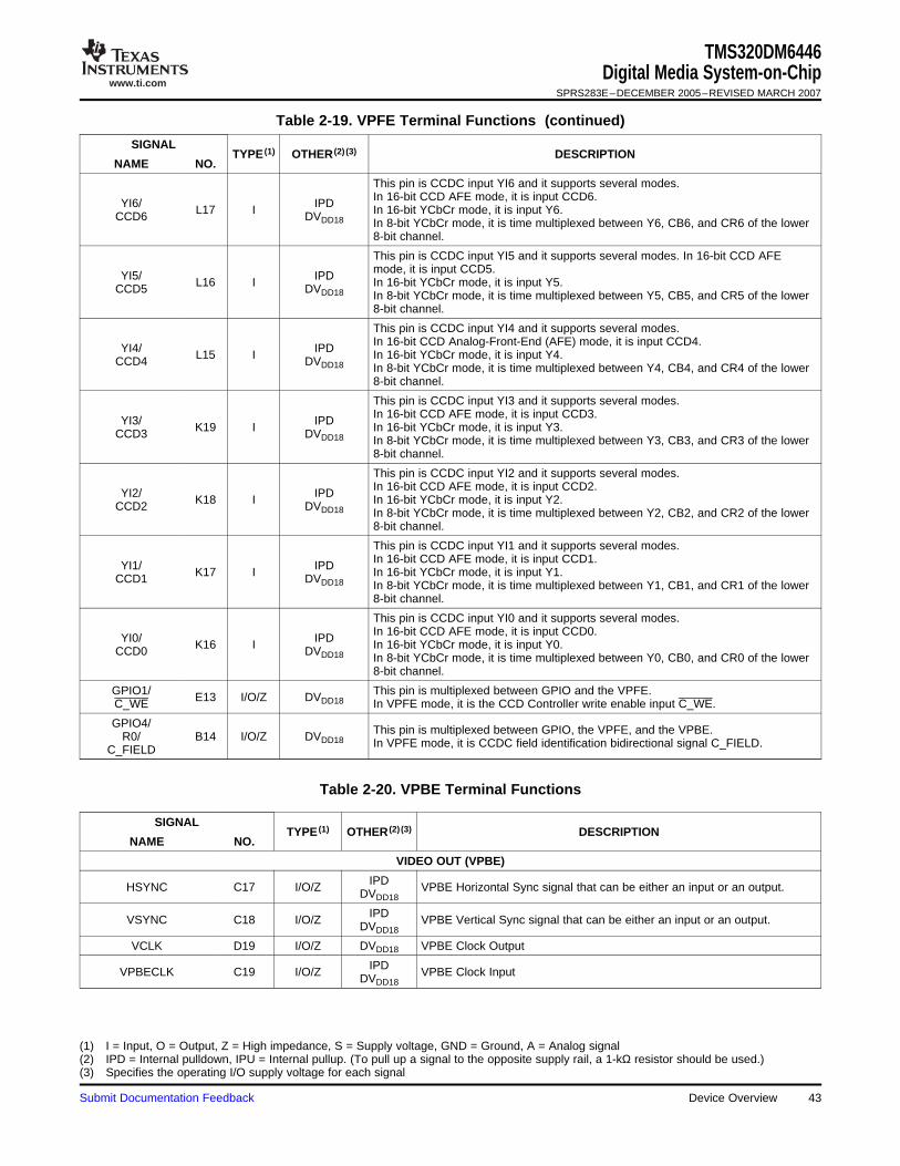
www.ti.com
TMS320DM6446Digital Media System-on-Chip
SPRS283E–DECEMBER 2005–REVISED MARCH 2007
Table 2-19. VPFE Terminal Functions (continued)
SIGNALTYPE (1) OTHER (2) (3) DESCRIPTION
NAME NO.
This pin is CCDC input YI6 and it supports several modes.In 16-bit CCD AFE mode, it is input CCD6.YI6/ IPDL17 I In 16-bit YCbCr mode, it is input Y6.CCD6 DVDD18 In 8-bit YCbCr mode, it is time multiplexed between Y6, CB6, and CR6 of the lower8-bit channel.
This pin is CCDC input YI5 and it supports several modes. In 16-bit CCD AFEmode, it is input CCD5.YI5/ IPDL16 I In 16-bit YCbCr mode, it is input Y5.CCD5 DVDD18 In 8-bit YCbCr mode, it is time multiplexed between Y5, CB5, and CR5 of the lower8-bit channel.
This pin is CCDC input YI4 and it supports several modes.In 16-bit CCD Analog-Front-End (AFE) mode, it is input CCD4.YI4/ IPDL15 I In 16-bit YCbCr mode, it is input Y4.CCD4 DVDD18 In 8-bit YCbCr mode, it is time multiplexed between Y4, CB4, and CR4 of the lower8-bit channel.
This pin is CCDC input YI3 and it supports several modes.In 16-bit CCD AFE mode, it is input CCD3.YI3/ IPDK19 I In 16-bit YCbCr mode, it is input Y3.CCD3 DVDD18 In 8-bit YCbCr mode, it is time multiplexed between Y3, CB3, and CR3 of the lower8-bit channel.
This pin is CCDC input YI2 and it supports several modes.In 16-bit CCD AFE mode, it is input CCD2.YI2/ IPDK18 I In 16-bit YCbCr mode, it is input Y2.CCD2 DVDD18 In 8-bit YCbCr mode, it is time multiplexed between Y2, CB2, and CR2 of the lower8-bit channel.
This pin is CCDC input YI1 and it supports several modes.In 16-bit CCD AFE mode, it is input CCD1.YI1/ IPDK17 I In 16-bit YCbCr mode, it is input Y1.CCD1 DVDD18 In 8-bit YCbCr mode, it is time multiplexed between Y1, CB1, and CR1 of the lower8-bit channel.
This pin is CCDC input YI0 and it supports several modes.In 16-bit CCD AFE mode, it is input CCD0.YI0/ IPDK16 I In 16-bit YCbCr mode, it is input Y0.CCD0 DVDD18 In 8-bit YCbCr mode, it is time multiplexed between Y0, CB0, and CR0 of the lower8-bit channel.
GPIO1/ This pin is multiplexed between GPIO and the VPFE.E13 I/O/Z DVDD18C_WE In VPFE mode, it is the CCD Controller write enable input C_WE.
GPIO4/ This pin is multiplexed between GPIO, the VPFE, and the VPBE.R0/ B14 I/O/Z DVDD18 In VPFE mode, it is CCDC field identification bidirectional signal C_FIELD.C_FIELD
Table 2-20. VPBE Terminal Functions
SIGNALTYPE (1) OTHER (2) (3) DESCRIPTION
NAME NO.
VIDEO OUT (VPBE)
IPDHSYNC C17 I/O/Z VPBE Horizontal Sync signal that can be either an input or an output.DVDD18
IPDVSYNC C18 I/O/Z VPBE Vertical Sync signal that can be either an input or an output.DVDD18
VCLK D19 I/O/Z DVDD18 VPBE Clock Output
IPDVPBECLK C19 I/O/Z VPBE Clock InputDVDD18
(1) I = Input, O = Output, Z = High impedance, S = Supply voltage, GND = Ground, A = Analog signal(2) IPD = Internal pulldown, IPU = Internal pullup. (To pull up a signal to the opposite supply rail, a 1-kΩ resistor should be used.)(3) Specifies the operating I/O supply voltage for each signal
Submit Documentation Feedback Device Overview 43

www.ti.com
TMS320DM6446Digital Media System-on-ChipSPRS283E–DECEMBER 2005–REVISED MARCH 2007
Table 2-20. VPBE Terminal Functions (continued)
SIGNALTYPE (1) OTHER (2) (3) DESCRIPTION
NAME NO.
COUT0/ This pin is multiplexed between ARM boot mode and the VPBE.IPDB3/ A16 I/O/Z After reset, this pin is either video encoder outputs COUT0, orDVDD18BTSEL0 RGB666/888 Blue output data bits 3, B3.
COUT1/ This pin is multiplexed between ARM boot mode and the VPBE.IPDB4/ B16 I/O/Z After reset, this pin is either video encoder outputs COUT1, orDVDD18BTSEL1 RGB666/888 Blue output data bits 4, B4.
COUT2/ This pin is multiplexed between EMIFA and the VPBE.IPDB5/ A17 I/O/Z After reset, it is video encoder output COUT2 or RGB666/888 Blue outputDVDD18EM_WIDTH data bit 5 B5.
COUT3/ This pin is multiplexed between DSP boot and the VPBE.IPDB6/ B17 I/O/Z After reset, it is video encoder output COUT3 or RGB666/888 Blue data bitDVDD18DSP_BT 6 output B6.
COUT4/ A18 O DVDD18 Video encoder output COUT4 or RGB666/888 Blue data bit 7 output B7.B7
COUT5/ B18 O DVDD18 Video encoder output COUT5 or RGB666/888 Green data bit 2 output G2.G2
COUT6/ B19 O DVDD18 Video encoder output COUT6 or RGB666/888 Green data bit 3 output G3.G3
COUT7/ C16 O DVDD18 Video encoder output COUT7 or RGB666/888 Green data bit 4 output G4.G4
YOUT0/ IPDG5/ D15 I/O/Z DVDD18AEAW0
YOUT1/ IPDG6/ D16 I/O/Z DVDD18AEAW1
YOUT2/ These pins are multiplexed between EMIFA and the VPBE.IPDG7/ D17 I/O/Z After reset, these are video encoder outputs YOUT[0:4] or RGB666/888DVDD18AEAW2 Red and Green data bit outputs G5, G6, G7, R3, and R4.
YOUT3/ IPDR3/ D18 I/O/Z DVDD18AEAW3
YOUT4/ IPDR4/ E15 I/O/Z DVDD18AEAW4
YOUT5/ E16 O DVDD18 Video encoder output YOUT5 or RGB666/888 Red data bit 5 output R5.R5
YOUT6/ E17 O DVDD18 Video encoder output YOUT6 or RGB666/888 Red data bit 6 output R6.R6
YOUT7/ E18 O DVDD18 Video encoder output YOUT7 or RGB666/888 Red data bit 7 output R7.R7
GPIO0/ This pin is multiplexed between GPIO and the VPBE.C13 I/O/Z DVDD18LCD_OE In VPBE mode, it is the LCD output enable LCD_OE.
GPIO2/ This pin is multiplexed between GPIO and the VPBE.D13 I/O/Z DVDD18G0 In VPBE mode, it is RGB888 Green data bit 0 output G0.
GPIO3/ This pin is multiplexed between GPIO, and the VPBE.B0/ C14 I/O/Z DVDD18 In VPBE mode, it is RGB888 Blue data bit 0 output B0 or LCD interlaced
LCD_FIELD bidirectional LCD_FIELD.
GPIO4/ This pin is multiplexed between GPIO, the VPFE, and the VPBE.R0/ B14 I/O/Z DVDD18 In VPBE mode, it is RGB888 Red data bit 0 output R0.C_FIELD
GPIO5/ This pin is multiplexed between GPIO and the VPBE.E14 I/O/Z DVDD18G1 In VPBE mode, it is RGB888 Green data bit 1 output G1.
GPIO6/ This pin is multiplexed between GPIO and the VPBE.A14 I/O/Z DVDD18B1 In VPBE mode, it is RGB888 Blue data bit 1 output B1.
GPIO38/ This pin is multiplexed between VPBE and GPIO.D14 I/O/Z DVDD18R1 In VPBE mode, it is RGB888 Red output data bit 1.
Device Overview44 Submit Documentation Feedback

www.ti.com
TMS320DM6446Digital Media System-on-Chip
SPRS283E–DECEMBER 2005–REVISED MARCH 2007
Table 2-20. VPBE Terminal Functions (continued)
SIGNALTYPE (1) OTHER (2) (3) DESCRIPTION
NAME NO.
PWM1/ This pin is multiplexed between PWM1, VPBE, and GPIO.R2/ B15 I/O/Z DVDD18 In VPBE mode, it is RGB888 Red output bit 2 (R2).GPIO46
PWM2/ This pin is multiplexed between PWM2, VPBE, and GPIO.B2/ A15 I/O/Z DVDD18 In VPBE mode, it is RGB888 Blue output bit 2 (B2).GPIO47
Table 2-21. DAC [Part of VPBE] Terminal Functions
SIGNALTYPE (1) OTHER (2) (3) DESCRIPTION
NAME NO.
DAC[A:D]
Reference voltage input (0.5 V). When the DAC is not used, the DAC_VREF signalDAC_VREF R17 A I (3)should be connected to VSS.
Output of DAC A. When the DAC is not used, the DAC_IOUT_A signal should beDAC_IOUT_A P19 A O left as a No Connect.
Output of DAC B. When the DAC is not used, the DAC_IOUT_B signal should beDAC_IOUT_B P18 A O left as a No Connect.
Output of DAC C. When the DAC is not used, the DAC_IOUT_C signal should beDAC_IOUT_C R19 A O left as a No Connect.
Output of DAC D. When the DAC is not used, the DAC_IOUT_D signal should beDAC_IOUT_D T19 A O left as a No Connect.
1.8-V analog I/O power. When the DAC is not used, the VDDA_1P8V signal should beVDDA_1P8V R18 S (3)connected to VSS.
Analog I/O ground. When the DAC is not used, the VSSA_1P8V signal should beVSSA_1P8V P17 GND (3)connected to VSS.
1.20-V analog core supply voltage (-594 device). When the DAC is not used, theVDDA_1P1V P16 S (3)VDDA_1P1V signal should be connected to VSS.
Analog core ground. When the DAC is not used, the VSSA_1P1V signal should beVSSA_1P1V T18 GND (3)connected to VSS.
External resistor connection for current bias configuration. This pin must beDAC_RBIAS R16 A I (3) connected via a 4-kΩ resistor to VSSA_1P8V. When the DAC is not used, the
DAC_RBIAS signal should be connected to VSS.
(1) I = Input, O = Output, Z = High impedance, S = Supply voltage, GND = Ground, A = Analog signal(2) Specifies the operating I/O supply voltage for each signal(3) For more information, see the Recommended Operating Conditions table
Submit Documentation Feedback Device Overview 45

www.ti.com
TMS320DM6446Digital Media System-on-ChipSPRS283E–DECEMBER 2005–REVISED MARCH 2007
Table 2-22. UART0, UART1, UART2 Terminal Functions
SIGNALTYPE (1) OTHER (2) (3) DESCRIPTION
NAME NO.
UART2
CI7/ IPD This pin is multiplexed between the CCDC and UART2.CCD15/ N19 I/O/Z DVDD18 When used by UART2 it is the receive data input UART_RXD2.UART_RXD2
CI6/ IPD This pin is multiplexed between the CCDC and UART2.CCD14/ N18 I/O/Z DVDD18 In UART2 mode, it is the transmit data output UART_TXD2.UART_TXD2
CI5/ IPD This pin is multiplexed between the CCDC and UART2.CCD13/ N17 I/O/Z DVDD18 In UART2 mode, it is the clear to send input UART_CTS2.UART_CTS2
CI4/ IPD This pin is multiplexed between the CCDC and UART2.CCD12/ N16 I/O/Z DVDD18 In UART2 mode, it is the ready to send output UART_RTS2.UART_RTS2
UART1
DMACK/ This pin is multiplexed between ATA/CF and UART1.H3 I/O/Z DVDD18UART_TXD1 For UART1, it is transmit data output UART_TXD1.
DMARQ/ IPD This pin is multiplexed between ATA/CF and UART1.G1 I/O/ZUART_RXD1 DVDD18 For UART1, it is receive data input UART_RXD1.
UART0
UART_RXD0/ This pin is multiplexed between UART0 and GPIO.D5 I/O/Z DVDD18GPIO35 For UART0, it is receive data input UART_RXD0.
UART_TXD0/ This pin is multiplexed between UART0 and GPIO. .C5 I/O/Z DVDD18GPIO36 For UART0, it is transmit data output UART_TXD0.
(1) I = Input, O = Output, Z = High impedance, S = Supply voltage, GND = Ground, A = Analog signal(2) IPD = Internal pulldown, IPU = Internal pullup. (To pull up a signal to the opposite supply rail, a 1-kΩ resistor should be used.)(3) Specifies the operating I/O supply voltage for each signal
Device Overview46 Submit Documentation Feedback

www.ti.com
TMS320DM6446Digital Media System-on-Chip
SPRS283E–DECEMBER 2005–REVISED MARCH 2007
Table 2-23. PWM0, PWM1, PWM2 Terminal Functions
SIGNALTYPE (1) OTHER (2) DESCRIPTION
NAME NO.
PWM2
PWM2/ This pin is multiplexed between PWM2, VPBE, and GPIO.B2/ A15 I/O/Z DVDD18 For PWM2, it is output PWM2.GPIO47
PWM1
PWM1/ This pin is multiplexed between PWM1, VPBE, and GPIO.R2/ B15 I/O/Z DVDD18 For PWM1, it is output PWM1.GPIO46
PWM0
PWM0/ This pin is multiplexed between PWM0 and GPIO.C15 I/O/Z DVDD18GPIO45 For PWM0, it is output PWM0.
(1) I = Input, O = Output, Z = High impedance, S = Supply voltage, GND = Ground, A = Analog signal(2) Specifies the operating I/O supply voltage for each signal
Table 2-24. ATA/CF Terminal Functions
SIGNALTYPE (1) OTHER (2) (3) DESCRIPTION
NAME NO.
ATA/CF
SPI_EN1/ This pin is multiplexed between SPI, ATA, and GPIO.HDDIR/ B2 I/O/Z DVDD18 For ATA, it is buffer direction control output HDDIR.GPIO42
GPIO50/ This pin is multiplexed between GPIO and ATA/CF.J5 O DVDD18ATA_CS0 In ATA mode, it is ATA/CF chip select output ATA_CS0.
GPIO51/ This pin is multiplexed between GPIO and ATA/CF.H1 O DVDD18ATA_CS1 In ATA mode, it is ATA/CF chip select output ATA_CS1.
EM_R/W/ This pin is multiplexed between EMIFA and ATA/CF.G3 I DVDD18INTRQ For ATA/CF, it is interrupt request input INTRQ.
EM_WAIT/ IPU This pin is multiplexed between EMIFA (NAND/SmartMedia/xD) and ATA/CF.(RDY/BSY)/ F1 I DVDD18 For ATA/CF, it is IO Ready input IORDY.IORDY
EM_OE/ This pin is multiplexed between EMIFA (NAND/SmartMedia/xD) and ATA/CF.(RE)/ H4 O DVDD18 For CF, it is read strobe output (IORD).(IORD)/ For ATA, it is read strobe output DIOR.DIOR
EM_WE This pin is multiplexed between EMIFA (NAND/SmartMedia/xD) and ATA/CF.(WE) G2 O DVDD18 For CF, it is write strobe output (IOWR).(IOWR)/ For ATA, it is write strobe output DIOW.DIOW
DMACK/ This pin is multiplexed between ATA/CF and UART1.H3 O DVDD18UART_TXD1 For ATA/CF, it is DMA acknowledge output DMACK.
DMARQ/ IPD This pin is multiplexed between ATA/CF and UART1.G1 OUART_RXD1 DVDD18 For ATA/CF, it is DMA request DMARQ input.
(1) I = Input, O = Output, Z = High impedance, S = Supply voltage, GND = Ground, A = Analog signal(2) IPD = Internal pulldown, IPU = Internal pullup. (To pull up a signal to the opposite supply rail, a 1-kΩ resistor should be used.)(3) Specifies the operating I/O supply voltage for each signal
Submit Documentation Feedback Device Overview 47

www.ti.com
TMS320DM6446Digital Media System-on-ChipSPRS283E–DECEMBER 2005–REVISED MARCH 2007
Table 2-24. ATA/CF Terminal Functions (continued)
SIGNALTYPE (1) OTHER (2) (3) DESCRIPTION
NAME NO.
EM_D15/ E1DD15
EM_D14/ H5DD14
EM_D13/ F2DD13
EM_D12/ D1DD12
EM_D11/ G4DD11
EM_D10/ G5DD10
EM_D9/ E2DD9
EM_D8/ F3 These pins are multiplexed between EMIFA (NAND) and ATA/CF. In all cases theyDD8I/O/Z DVDD18 are used as a 16 bit bi-directional data bus.
EM_D7/ For ATA/CF, these are DD[15:0].C1DD7
EM_D6/ F4DD6
EM_D5/ D2DD5
EM_D4/ E4DD4
EM_D3/ E3DD3
EM_D2/ F5DD2
EM_D1/ D3DD1
EM_D0/ E5DD0
EM_A[0]/ This pin is multiplexed between EMIFA, ATA/CF, and GPIO.DA2/ J4 I/O/Z DVDD18 For ATA/CF, it is Device address bit 2 output DA2.GPIO53
EM_BA[1]/ This pin is multiplexed between EMIFA, ATA/CF, and GPIO.DA1/ H2 I/O/Z DVDD18 For ATA/CF, it is Device address bit 1 output DA1.GPIO52
EM_BA[0]/ This pin is multiplexed between EMIFA and ATA/CF.J3 I/O/Z DVDD18DA0 For ATA/CF, it is Device address bit 0 output DA0.
Device Overview48 Submit Documentation Feedback

www.ti.com
TMS320DM6446Digital Media System-on-Chip
SPRS283E–DECEMBER 2005–REVISED MARCH 2007
Table 2-25. MMC/SD/SDIO Terminal Functions
SIGNALTYPE (1) OTHER (2) DESCRIPTION
NAME NO.
MMC/SD/SDIO
SD_CLK A9 O DVDD33 Data clock output SD_CLK
SD_CMD B9 I/O/Z DVDD33 Bi-directional command IO SD_CMD
SD_DATA3 C9 I/O/Z
SD_DATA2 D9 I/O/ZDVDD33 These pins are the nibble wide bi-directional data bus SD_DATA[3:0].
SD_DATA1 E9 I/O/Z
SD_DATA0 D8 I/O/Z
(1) I = Input, O = Output, Z = High impedance, S = Supply voltage, GND = Ground, A = Analog signal(2) Specifies the operating I/O supply voltage for each signal
Submit Documentation Feedback Device Overview 49

www.ti.com
TMS320DM6446Digital Media System-on-ChipSPRS283E–DECEMBER 2005–REVISED MARCH 2007
Table 2-26. HPI Terminal Functions
SIGNALTYPE (1) OTHER (2) (3) DESCRIPTION
NAME NO.
Host-Port Interface (HPI)
For EMIFA, this pin is Chip Select 3 output.EM_CS3 B1 I/O/Z DVDD18 In HPI mode this pin must be pulled high via an external 10-kΩ resistor.
EM_BA[0]/ This pin is multiplexed between EMIFA, ATA/CF, and HPI.DA0/ J3 I/O/Z DVDD18 In HPI mode, it is the host interrupt output HINT.HINT
EM_A[0]/ This pin is multiplexed between EMIFA, ATA/CF, HPI, and GPIO.DA2/ For HPI, it is control input HCNTL1. The state of HCNTL1 and HCNTL0 determineJ4 I/O/Z DVDD18HCNTL1/ if address, data, or control information is being transmitted between an external
GPIO53 host and DM644X.
This pin is multiplexed between EMIFA (NAND/SmartMedia/xD), and HPI.EM_A[2]/ In HPI mode, it is control input HCNTL0. The state of HCNTL1 and HCNTL0(CLE)/ J1 I/O/Z DVDD18 determine if address, data, or control information is being transmitted between anHCNTL0 external host and DM644X.
EM_A[1]/ This pin is multiplexed between EMIFA (NAND/SmartMedia/xD), and HPI.(ALE)/ J2 I/O/Z DVDD18 In HPI mode, it is Half-word identification input HHWIL.HHWIL
EM_R/W/ This pin is multiplexed between EMIFA, ATA/CF, and HPI.INTRQ/ G3 I/O/Z DVDD18 For HPI, it is the Host Read Write input HR/W. This signal is active high for readsHR/W and low for writes.
EM_CS2/ This pin is multiplexed between EMIFA and HPI.C2 I/O/Z DVDD18HCS In HPI mode, this pin is HPI Active Low Chip Select input HCS.
EM_WE(WE) This pin is multiplexed between EMIFA (NAND/SmartMedia/xD), ATA/CF, and HPI.(IOWR)/ G2 I/O/Z DVDD18 For HPI, it is data strobe 2 input HDS2.DIOW/HDS2
EM_OE/(RE)/ This pin is multiplexed between EMIFA (NAND/SmartMedia/xD), ATA/CF, and HPI.(IORD)/ H4 I/O/Z DVDD18 For HPI, it is data strobe 1 input HDS1.DIOR/HDS1
EM_WAIT/(RDY/BSY)/ IPU This pin is multiplexed between EMIFA (NAND/SmartMedia/xD), ATA/CF, and HPI.F1 I/O/ZIORDY/ DVDD18 For HPI, it is ready output HRDY.
HRDY
(1) IPD = Internal pulldown, IPU = Internal pullup. (To pull up a signal to the opposite supply rail, a 1-kΩ resistor should be used.)(2) I = Input, O = Output, Z = High impedance, S = Supply voltage, GND = Ground, A = Analog signal(3) Specifies the operating I/O supply voltage for each signal
Device Overview50 Submit Documentation Feedback

www.ti.com
TMS320DM6446Digital Media System-on-Chip
SPRS283E–DECEMBER 2005–REVISED MARCH 2007
Table 2-26. HPI Terminal Functions (continued)
SIGNALTYPE (1) OTHER (2) (3) DESCRIPTION
NAME NO.
EM_D15/DD15/ E1HD15
EM_D14/DD14/ H5HD14
EM_D13/DD13/ F2HD13
EM_D12/DD12/ D1HD12
EM_D11/DD11/ G4HD11
EM_D10/DD10/ G5HD10
EM_D9/DD9/ E2HD9
EM_D8/DD8/ F3
These pins are multiplexed between EMIFA (NAND), ATA/CF, and HPI.HD8I/O/Z DVDD18 In HPI mode, these are HD[15:0] and are multiplexed internally with the HPI
EM_D7/ address lines.DD7/ C1HD7
EM_D6/DD6/ F4HD6
EM_D5/DD5/ D2HD5
EM_D4/DD4/ E4HD4
EM_D3/DD3/ E3HD3
EM_D2/DD2/ F5HD2
EM_D1/DD1/ D3HD1
EM_D0/DD0/ E5HD0
Submit Documentation Feedback Device Overview 51

www.ti.com
TMS320DM6446Digital Media System-on-ChipSPRS283E–DECEMBER 2005–REVISED MARCH 2007
Table 2-27. Timer 0, Timer 1, and Timer 2 Terminal Functions
SIGNALTYPE (1) OTHER (2) DESCRIPTION
NAME NO.
Timer 2 and Timer 1
No external pins. The Timer 2 and Timer 1 peripheral pins are not pinned out as external pins.
Timer 0
CLK_OUT1/ This pin is multiplexed between the USB clock generator, timer, and GPIO.TIM_IN/ E19 I/O/Z DVDD18 For Timer0, it is the timer event capture input TIM_IN.GPIO49
(1) I = Input, O = Output, Z = High impedance, S = Supply voltage, GND = Ground, A = Analog signal(2) Specifies the operating I/O supply voltage for each signal
Table 2-28. Reserved Terminal Functions
SIGNALTYPE (1) OTHER (2) (3) DESCRIPTION
NAME NO.
RESERVED
RSV1 A1 Reserved. (Leave unconnected, do not connect to power or ground)
RSV2 A19 Reserved. (Leave unconnected, do not connect to power or ground)
RSV3 W1 Reserved. (Leave unconnected, do not connect to power or ground)
RSV4 W19 Reserved. (Leave unconnected, do not connect to power or ground)
IPDRSV5 D4 I Reserved. This pin must be tied directly to VSS for normal device operation.VSS
RSV6 L3 A O Reserved. (Leave unconnected, do not connect to power or ground)
RSV7 R8 A Reserved. (Leave unconnected, do not connect to power or ground)
RSV24 M3 S Reserved. (Leave unconnected, do not connect to power or ground)
(1) I = Input, O = Output, Z = High impedance, S = Supply voltage, GND = Ground, A = Analog signal(2) IPD = Internal pulldown, IPU = Internal pullup. (To pull up a signal to the opposite supply rail, a 1-kΩ resistor should be used.)(3) Specifies the operating I/O supply voltage for each signal
Table 2-29. Supply Terminal Functions
SIGNALTYPE (1) OTHER DESCRIPTION
NAME NO.
SUPPLY VOLTAGE PINS
F10
F11 3.3 V I/O supply voltageDVDD33 S (see the Power-Supply Decoupling section of this data manual)F12
F13
(1) I = Input, O = Output, Z = High impedance, S = Supply voltage, GND = Ground, A = Analog signal
Device Overview52 Submit Documentation Feedback

www.ti.com
TMS320DM6446Digital Media System-on-Chip
SPRS283E–DECEMBER 2005–REVISED MARCH 2007
Table 2-29. Supply Terminal Functions (continued)
SIGNALTYPE (1) OTHER DESCRIPTION
NAME NO.
N5
G15
F14
J15
H14
K14
M14
L13
G9 1.8 V I/O supply voltageDVDD18 S (see the Power-Supply Decoupling section of this data manual)F8
E7
G7
J7
L7
F6
H6
K6
M6
T5
P6
N7
P8
N9
R9
P10 1.8 V DDR2 I/O supply voltageDVDDR2 S (see the Power-Supply Decoupling section of this data manual)N11
R11
P12
N13
R13
P14
R15
F15
K12
M12
L11
M10 1.20 V core supply voltage (-594 device)CVDD S (see the Power-Supply Decoupling section of this data manual)L10
K10
L9
L8
M8
Submit Documentation Feedback Device Overview 53

www.ti.com
TMS320DM6446Digital Media System-on-ChipSPRS283E–DECEMBER 2005–REVISED MARCH 2007
Table 2-29. Supply Terminal Functions (continued)
SIGNALTYPE (1) OTHER DESCRIPTION
NAME NO.
J13
H12
H11
J11
K111.20 V DSPSS supply voltage (-594 devices)CVDDDSP J10 S (see the Power-Supply Decoupling section of this data manual)
H10
J9
K9
K8
H8
Device Overview54 Submit Documentation Feedback

www.ti.com
TMS320DM6446Digital Media System-on-Chip
SPRS283E–DECEMBER 2005–REVISED MARCH 2007
Table 2-30. Ground Terminal Functions
SIGNALTYPE (1) OTHER DESCRIPTION
NAME NO.
GROUND PINS
K5
M5
G6
J6
L6
N6
R6
F7
H7
K7
M7
P7
R7
E8
G8
J8
N8
F9
H9
VSS M9 GND Ground pins
P9
G10
N10
R10
G11
M11
P11
G12
J12
N12
L12
R12
G13
H13
K13
M13
P13
G14
J14
(1) I = Input, O = Output, Z = High impedance, S = Supply voltage, GND = Ground, A = Analog signal
Submit Documentation Feedback Device Overview 55

www.ti.com
TMS320DM6446Digital Media System-on-ChipSPRS283E–DECEMBER 2005–REVISED MARCH 2007
Table 2-30. Ground Terminal Functions (continued)
SIGNALTYPE (1) OTHER DESCRIPTION
NAME NO.
L14
N14
R14VSS GND Ground pins
H15
K15
P15
56 Device Overview Submit Documentation Feedback

www.ti.com
2.8 Device Support
2.8.1 Development Support
2.8.2 Device and Development-Support Tool Nomenclature
TMS320DM6446Digital Media System-on-Chip
SPRS283E–DECEMBER 2005–REVISED MARCH 2007
TI offers an extensive line of development tools for the TMS320DM644x SoC platform, including tools toevaluate the performance of the processors, generate code, develop algorithm implementations, and fullyintegrate and debug software and hardware modules. The tool's support documentation is electronicallyavailable within the Code Composer Studio™ Integrated Development Environment (IDE).
The following products support development of TMS320DM644x SoC-based applications:
Software Development Tools:Code Composer Studio™ Integrated Development Environment (IDE): including EditorC/C++/Assembly Code Generation, and Debug plus additional development toolsScalable, Real-Time Foundation Software (DSP/BIOS™), which provides the basic run-time targetsoftware needed to support any SoC application.
Hardware Development Tools:Extended Development System (XDS™) EmulatorFor a complete listing of development-support tools for the TMS320DM644x SoC platform, visit theTexas Instruments web site on the Worldwide Web at http://www.ti.com uniform resource locator(URL). For information on pricing and availability, contact the nearest TI field sales office or authorizeddistributor.
To designate the stages in the product development cycle, TI assigns prefixes to the part numbers of allDSP devices and support tools. Each DSP commercial family member has one of three prefixes: TMX,TMP, or TMS (e.g., TMX320DM6446ZWT). Texas Instruments recommends two of three possible prefixdesignators for its support tools: TMDX and TMDS. These prefixes represent evolutionary stages ofproduct development from engineering prototypes (TMX/TMDX) through fully qualified productiondevices/tools (TMS/TMDS).
Device development evolutionary flow:
TMX Experimental device that is not necessarily representative of the final device's electricalspecifications.
TMP Final silicon die that conforms to the device's electrical specifications but has not completedquality and reliability verification.
TMS Fully-qualified production device.
Support tool development evolutionary flow:
TMDX Development-support product that has not yet completed Texas Instruments internalqualification testing.
TMDS Fully qualified development-support product.
TMX and TMP devices and TMDX development-support tools are shipped against the followingdisclaimer:
"Developmental product is intended for internal evaluation purposes."
TMS devices and TMDS development-support tools have been characterized fully, and the quality andreliability of the device have been demonstrated fully. TI's standard warranty applies.
Submit Documentation Feedback Device Overview 57

www.ti.com
DM644x DMSoC:DM6443DM6446
PREFIX DEVICE SPEED RANGE
TMS 320 DM6446 ZWT ( )
TMX = Experimental deviceTMS = Qualified device
DEVICE FAMILY320 = TMS320 DSP family
PACKAGE TYPE(A)
ZWT = 361-pin plastic BGA, with Pb-free soldered ballsDEVICE(B)
TEMPERATURE RANGE (DEFAULT: 0°C TO 85°C)
( )
Blank = 0°C to 85°C, commercial temperature
Blank = 594-MHz DSP, 297−MHz ARM9 [Default]
A. BGA = Ball Grid Array
B. For actual device part numbers (P/Ns) and ordering information, see the TI website (http://www.ti.com).
( )
SILICON REVISIONBlank = Silicon 1.3
TMS320DM6446Digital Media System-on-ChipSPRS283E–DECEMBER 2005–REVISED MARCH 2007
Predictions show that prototype devices (TMX or TMP) have a greater failure rate than the standardproduction devices. Texas Instruments recommends that these devices not be used in any productionsystem because their expected end-use failure rate still is undefined. Only qualified production devices areto be used.
TI device nomenclature also includes a suffix with the device family name. This suffix indicates thepackage type (for example, ZWT), the temperature range (for example, "Blank" is the commercialtemperature range), and the device speed range in megahertz (for example, "Blank" is the default[594-MHz DSP, 297-MHz ARM9]).
Figure 2-6 provides a legend for reading the complete device name for any TMS320DM644x SoC platformmember.
Figure 2-6. Device Nomenclature
58 Device Overview Submit Documentation Feedback

www.ti.com
2.8.3 Documentation Support
TMS320DM6446Digital Media System-on-Chip
SPRS283E–DECEMBER 2005–REVISED MARCH 2007
2.8.3.1 Related Documentation From Texas Instruments
The following documents describe the TMS320DM644x Digital Media System-on-Chip (DMSoC). Copiesof these documents are available on the Internet at www.ti.com. Tip: Enter the literature number in thesearch box provided at www.ti.com.
The current documentation that describes the DM644x DMSoC, related peripherals, and other technicalcollateral, is available in the C6000 DSP product folder at: www.ti.com/c6000.
SPRUE14 TMS320DM644x DMSoC ARM Subsystem Reference Guide. Describes the ARMsubsystem in the TMS320DM644x Digital Media System-on-Chip (DMSoC). The ARMsubsystem is designed to give the ARM926EJ-S (ARM9) master control of the device. Ingeneral, the ARM is responsible for configuration and control of the device; including theDSP subsystem, the video processing subsystem, and a majority of the peripherals andexternal memories.
SPRUE15 TMS320DM644x DMSoC DSP Subsystem Reference Guide. Describes the digital signalprocessor (DSP) subsystem in the TMS320DM644x Digital Media System-on-Chip (DMSoC).
SPRUE19 TMS320DM644x DMSoC Peripherals Overview Reference Guide. Provides an overviewand briefly describes the peripherals available on the TMS320DM644x Digital MediaSystem-on-Chip (DMSoC).
SPRAA84 TMS320C64x to TMS320C64x+ CPU Migration Guide. Describes migrating from the TexasInstruments TMS320C64x digital signal processor (DSP) to the TMS320C64x+ DSP. Theobjective of this document is to indicate differences between the two cores. Functionality inthe devices that is identical is not included.
SPRU732 TMS320C64x/C64x+ DSP CPU and Instruction Set Reference Guide. Describes the CPUarchitecture, pipeline, instruction set, and interrupts for the TMS320C64x and TMS320C64x+digital signal processors (DSPs) of the TMS320C6000 DSP family. The C64x/C64x+ DSPgeneration comprises fixed-point devices in the C6000 DSP platform. The C64x+ DSP is anenhancement of the C64x DSP with added functionality and an expanded instruction set.
SPRU871 TMS320C64x+ DSP Megamodule Reference Guide. Describes the TMS320C64x+ digitalsignal processor (DSP) megamodule. Included is a discussion on the internal direct memoryaccess (IDMA) controller, the interrupt controller, the power-down controller, memoryprotection, bandwidth management, and the memory and cache.
SPRAAA6 EDMA v3.0 (EDMA3) Migration Guide for TMS320DM644x DMSoC. Describes migratingfrom the Texas Instruments TMS320C64x digital signal processor (DSP) enhanced directmemory access (EDMA2) to the TMS320DM644x Digital Media System-on-Chip (DMSoC)EDMA3. This document summarizes the key differences between the EDMA3 and theEDMA2 and provides guidance for migrating from EDMA2 to EDMA3.
Submit Documentation Feedback Device Overview 59

www.ti.com
3 Device Configurations
3.1 System Module Registers
3.2 Power Considerations
3.2.1 Power Configurations at Reset
TMS320DM6446Digital Media System-on-ChipSPRS283E–DECEMBER 2005–REVISED MARCH 2007
The system module includes status and control registers required for configuration of the device. Briefdescriptions of the various registers are shown in Table 3-1. System Module registers required for deviceconfigurations are discussed in the following sections.
Table 3-1. System Module Register Memory Map
HEX ADDRESS RANGE REGISTER ACRONYM DESCRIPTION
0x01C4 0000 PINMUX0 Pin multiplexing control 0. For details, see Section 3.5.4, PINMUX0 RegisterDescription.
0x01C4 0004 PINMUX1 Pin multiplexing control 1. For details, see Section 3.5.5, PINMUX1 RegisterDescription.
0x01C4 0008 DSPBOOTADDR Boot address of DSP. For details, see Section 3.3.1.2, DSPBOOTADDRRegister Description.
0x01C4 000C SUSPSRC Emulator Suspend Source. For details, see Section 3.6, Emulation Control.
0x01C4 0010 INTGEN ARM/DSP Interrupt Status and Control. For details, see Section 6.7.3,ARM/DSP Communications Interrupts.
0x01C4 0014 BOOTCFG Device boot configuration. For details, see Section 3.3.1.1, BOOTCFGRegister Description.
0x01C4 0018 - 0x01C4 0027 – Reserved.
0x01C4 0028 JTAGID JTAGID/Device ID number. For details, see Section 6.25.1, JTAG ID RegisterDescription.
0x01C4 002C – Reserved.
0x01C4 0030 HPI_CTL HPI control. For details, see Section 3.5.6.10, HPI and EMIFA/ATA PinMultiplexing.
0x01C4 0034 USBPHY_CTL USB PHY control. For details, see Section 6.15.1, USBPHY_CTL RegisterDescription.
0x01C4 0038 CHP_SHRTSW Chip shorting switch control. For details, see Section 3.2.1, PowerConfigurations at Reset.
0x01C4 003C MSTPRI0 Bus master priority control 0. For details, see Section 3.5.1, Switched CentralResource (SCR) Bus Priorities.
0x01C4 0040 MSTPRI1 Bus master priority control 1. For details, see Section 3.5.1, Switched CentralResource (SCR) Bus Priorities.
0x01C4 0044 VPSS_CLKCTL VPSS clock control.
0x01C4 0048 VDD3P3V_PWDN VDD 3.3V I/O powerdown control. For details, see Section 3.2.2, PowerConfigurations after Reset.
0x01C4 004C DRRVTPER Enables access to the DDR2 VTP Register.
0x01C4 0050 - 0x01C4 006F – Reserved.
Global device power domains are controlled by the Power and Sleep Controller, except as shown in thefollowing sections.
As described in the DM6446 Power and Clock Domains section, the DM6446 has two power domains:Always On and DSP. There is a shorting switch between the two power domains that must be openedwhen the DSP domain is powered off and closed when the DSP domain is powered on.
The CHP_SHRTSW register, shown in Figure 3-1, controls the shorting switch between the devicealways-on and DSP power domains. This switch should be enabled after powering-up the DSP domain.
Device Configurations60 Submit Documentation Feedback

www.ti.com
3.2.2 Power Configurations after Reset
3.3 Bootmode
TMS320DM6446Digital Media System-on-Chip
SPRS283E–DECEMBER 2005–REVISED MARCH 2007
Setting the DSPPWRON bit to '1’ closes (enables) the switch and enables the DSP power domain. Thedefault switch value is determined by the DSP_BT configuration input. If DSP self boot is selected(DSP_BT=1), the DSP will be powered-up and DSPPWRON will be set to a value of '1'. For ARM bootoperation (DSP_BT=0), DSPPWRON will be set to the disable value of '0' and must be set by the ARMbefore the DSP domain power is turned on.
Note: Once the DSP power domain is enabled (powered up), it cannot be disabled (powered down).Dynamic power down of the DSP is not supported on this device.
Figure 3-1. CHP_SHRTSW Register31 1 0
RESERVED DSPPWRON
R-0000 0000 0000 0000 0000 0000 0000 000 R/W-L
LEGEND: R = Read, W = Write, n = value at reset, L = pin state latched at reset rising
Table 3-2. CHP_SHRTSW Register Description
NAME DESCRIPTION
DSPPWRON DSP power domain enable.0 = DSP power domain off1 = DSP power domain on
The VDD3P3V_PWDN register controls power to the 3.3V I/O buffers for MMC/SD/SDIO and GPIOV33.The 3.3V I/Os are separated into two groups for independent control as shown in Figure 3-2 anddescribed in Table 3-3. By default, these pins are all disabled at reset.
Figure 3-2. VDD3P3V_PWDN Register31 2 1 0
RESERVED IOPWDN1 IOPWDN0
R-0000 0000 0000 0000 0000 0000 0000 00 R/W-1 R/W-1
LEGEND: R = Read, W = Write, n = value at reset
Table 3-3. VDD3P3V_PWDN Register Description
NAME DESCRIPTION
IOPWDN0 GIOV33 I/O Powerdown controls GIOV33[16:0] pins.0 = I/O buffers powered up1 = I/O buffers powered down
IOPWDN1 MMC/SD/SDIO I/O Powerdown controls SD_CLK, SD_CMD, SD_DATA[3:0] pins.0 = I/O buffers powered up1 = I/O buffers powered down
The device is booted through multiple means: pin states captured at reset, primary bootloaders withininternal ROM or EMIFA, and secondary user bootloaders from peripherals or external memories. Bootmodes, pin configurations, and register configurations required for booting the device, are described in thefollowing sections.
Submit Documentation Feedback Device Configurations 61

www.ti.com
3.3.1 Bootmode Registers
TMS320DM6446Digital Media System-on-ChipSPRS283E–DECEMBER 2005–REVISED MARCH 2007
The BOOTCFG and DSPBOOTADDR registers are described in the following sections. At reset, the statusof various pins required for proper boot are stored within these registers.
3.3.1.1 BOOTCFG Register Description
The BOOTCFG register (located at address 0x01C4 000A) contains the status values of the BTSEL1,BTSEL0, DSP_BT, EM_WIDTH, and AEAW[4:0] pins captured at the rising edge of RESET. The registerformat is shown in Figure 3-3 and bit field descriptions are shown in Table 3-4. The captured bits aresoftware readable after reset.
Figure 3-3. BOOTCFG Register
31 9 8 7 6 5 4 3 2 1 0
RESERVED DSP_BT BTSEL EM_WIDTH DAEAW
R-0000 0000 0000 0000 0000 000 R-L R-LL R-L R-LLLLL
LEGEND: R = Read; W = Write; L = pin state latched at reset rising; -n = value after reset
Table 3-4. BOOTCFG Register Description
NAME DESCRIPTION
BTSEL ARM Boot mode selection pin states (BTSEL1, BTSEL0) captured at the rising edge of RESET.
‘00’ indicates ARM boots from ROM (NAND Flash).‘01’ indicates that ARM boots from EMIFA (NOR Flash).‘10’ indicates that ARM boots from ROM (HPI).‘11’ indicates that ARM boots from ROM (UART0).
DSP_BT DSP Boot mode selection pin state captured at the rising edge of RESET.
‘0’ sets ARM boot of C64x+.‘1’ sets C64x+ self boot.
EM_WIDTH EMIFA data bus width selection pin state captured at the rising edge of RESET.
‘0’ sets EMIFA to 8 bit data bus width‘1’ sets EMIFA to 16 bit data bus width.
DAEAW EMIFA address bus width selection pin states (AEAW[4:0]) captured at the rising edge of RESET. This configuresEMIFA address pins multiplexed with GPIO. See Table 3-9,Table 3-10, and Table 3-11
3.3.1.2 DSPBOOTADDR Register Description
The DSPBOOTADDR register contains the upper 22 bits of the C64x+ DSP reset vector. The registerformat is shown in Figure 3-4 and bit field descriptions are shown in Table 3-5. DSPBOOTADDR isreadable and writable by software after reset.
Figure 3-4. DSPBOOTADDR Registers
31 10 9 0
BOOTADDR[21:0] RESERVED
R- 0100 0010 0010 0000 0000 00 R-00 0000 0000
LEGEND: R/W = Read/Write; R = Read only; -n = value after reset
Table 3-5. DSPBOOTADDR Register Description
NAME DESCRIPTION
BOOTADDR[21:0] Upper 22 bits of the C64x+ DSP boot address.
Device Configurations62 Submit Documentation Feedback

www.ti.com
3.3.2 ARM Boot
3.3.3 DSP Boot
TMS320DM6446Digital Media System-on-Chip
SPRS283E–DECEMBER 2005–REVISED MARCH 2007
The DM6446 ARM can boot from EMIFA, internal ROM (NAND), UART0, or HPI, as determined by thesetting of the BTSEL[1:0] pins. The BTSEL[1:0] pins are read by the ARM ROM Boot Loader (RBL) tofurther define the ROM boot mode. The ARM boot modes are summarized in Table 3-6.
Table 3-6. ARM Boot Modes
BTSEL1 BTSEL0 BOOT MODE ARM RESET BRIEF DESCRIPTIONVECTOR
0 0 ARM NAND RBL 0x0000 4000 Up to 14 K-bytes secondary boot loader through NAND with upto 2 K-bytes page sizes.
0 1 ARM EMIFA External Boot 0x0200 0000 EMIFA EM_CS2 external memory space.
1 0 ARM HPI RBL 0x0000 4000 Up to 14 K-btyes secondary boot loader through an externalhost.
1 1 ARM UART RBL 0x0000 4000 Up to 14 K-bytes secondary boot loader through UART0.
When the BTSEL[1:0] pins are set to the ARM EMIFA External Boot ("01"), the ARM immediately beginsexecuting code from the EMIFA EM_CS2 memory space (0x0200 0000). When the BTSEL[1:0] pinsindicate a condition other than the ARM EMIFA External Boot (!01), the RBL begins execution.
ARM NAND Boot mode has the following features:• Loads a secondary User Boot Loader (UBL) from NAND flash to ARM Internal RAM (AIM) and
transfers control to the user software.• Support for NAND with page sizes up to 2048 bytes.• Support for error correction when loading UBL• Support for up to 14KB UBL• Optional, user selectable, support for use of DMA, I-cache, and PLL enable while loading UBL
ARM UART Boot mode has the following features:• Loads a secondary UBL via UART0 to AIM and transfers control to the user software.• Support for up to 14KB UBL
ARM HPI Boot Mode has the following features:• No support for a full firmware boot. Instead, waits for external host to load a secondary UBL via HPI to
AIM and transfers control to the user software.• Support for up to 14KB UBL.
For further details on the ROM Bootloader, refer to the ARM Subsystem Users Guide.
For C64x+ booting, the state of the DSP_BT pin is sampled at reset. If DSP_BT is low, the ARM will bethe master of C64x+ and control booting (Host Boot mode). If DSP_BT is high, the C64x+ will boot itselfcoming out of device reset (Self-Boot mode). Table 3-7 shows a summary of the DSP boot modes.
Table 3-7. DSP Boot Modes
DSP_BT DSP ARM DSPBOOTADDR BRIEF DESCRIPTIONBOOT MODE BOOT MODE REGISTER VALUE
0 Host Boot Internal Boot Programmable ARM sets an internal DSP memory location in DSPBOOTADDRregister where valid DSP code resides and loads code to thisinternal DSP memory through DMA prior to releasing DSP reset.
0 Host Boot External Boot Programmable ARM sets an external DSP memory location in DSPBOOTADDRregister (EMIFA or DDR2) where valid DSP code resides prior toreleasing DSP reset.
1 Self Boot Any, except HPI 0x4220 0000 Default EMIFA Base Address
Submit Documentation Feedback Device Configurations 63
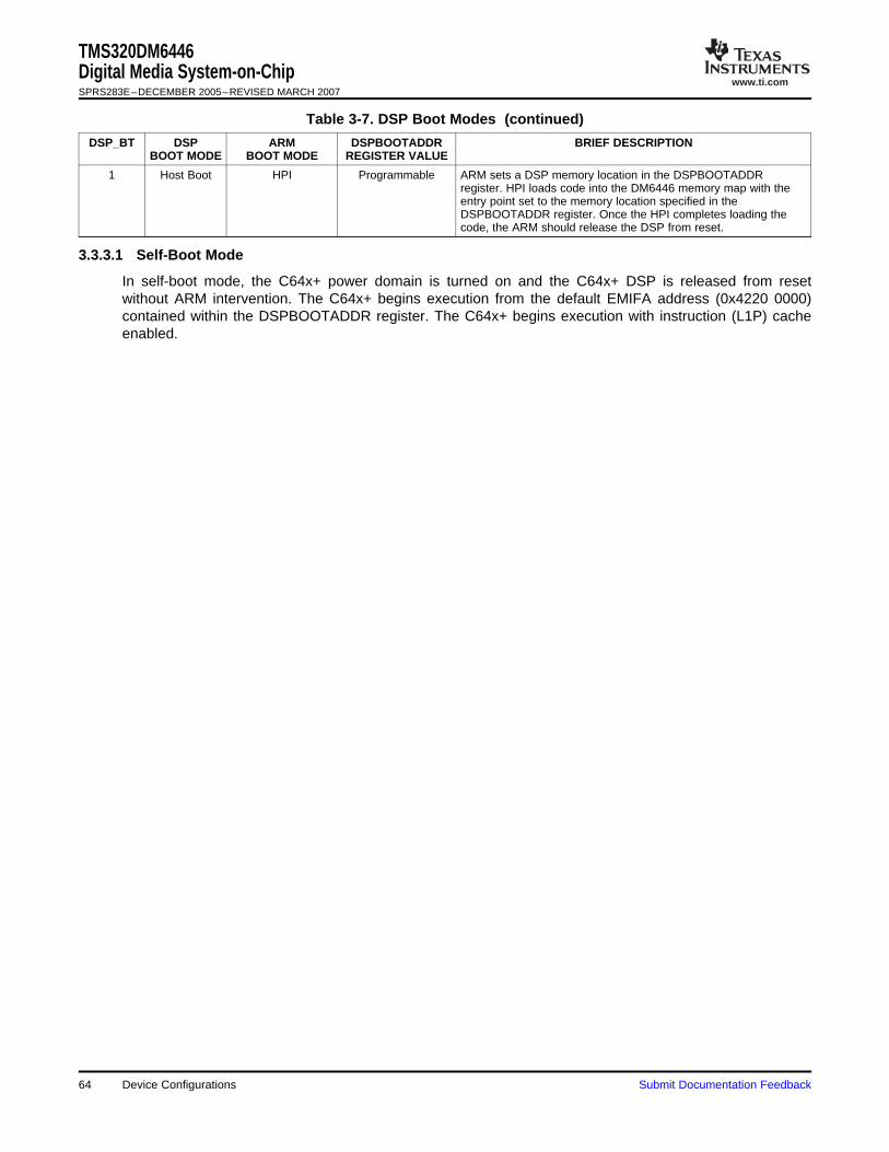
www.ti.com
TMS320DM6446Digital Media System-on-ChipSPRS283E–DECEMBER 2005–REVISED MARCH 2007
Table 3-7. DSP Boot Modes (continued)
DSP_BT DSP ARM DSPBOOTADDR BRIEF DESCRIPTIONBOOT MODE BOOT MODE REGISTER VALUE
1 Host Boot HPI Programmable ARM sets a DSP memory location in the DSPBOOTADDRregister. HPI loads code into the DM6446 memory map with theentry point set to the memory location specified in theDSPBOOTADDR register. Once the HPI completes loading thecode, the ARM should release the DSP from reset.
3.3.3.1 Self-Boot Mode
In self-boot mode, the C64x+ power domain is turned on and the C64x+ DSP is released from resetwithout ARM intervention. The C64x+ begins execution from the default EMIFA address (0x4220 0000)contained within the DSPBOOTADDR register. The C64x+ begins execution with instruction (L1P) cacheenabled.
64 Device Configurations Submit Documentation Feedback

www.ti.com
3.4 Configurations at Reset
3.4.1 Device Configuration at Device Reset
3.4.2 Peripheral Selection at Device Reset
TMS320DM6446Digital Media System-on-Chip
SPRS283E–DECEMBER 2005–REVISED MARCH 2007
The following sections give information on configuration settings for the device at reset.
Table 3-8 shows a summary of device inputs required for booting the ARM and DSP, and configuringEMIFA data and address bus widths for proper operation of the device at the rising edge of the RESETinput.
Table 3-8. Device Configurations (Input Pins Sampled at Reset)
DEVICE SIGNALS DEVICE SIGNAL NAMESAMPLED DESCRIPTIONAFTER RESETAT RESET
BTSEL[1:0] COUT[1:0] ARM Boot mode selection pins.
‘00’ indicates ARM boots from ROM (NAND Flash).‘01’ indicates that ARM boots from EMIFA (NOR Flash).‘10’ indicates that the ARM boots from the HPI (ROM)‘11’ indicates that ARM boots from ROM (UART0).
DSP_BT COUT3 DSP Boot mode selection pin.
‘0’ sets ARM boot of C64x+.‘1’ sets C64x+ self boot.
EM_WIDTH COUT2 EMIFA data bus width selection pin.
‘0’ sets EMIFA to 8-bit data bus width‘1’ sets EMIFA to 16-bit data bus width.
AEAW[4:0] YOUT[4:0] EMIFA address bus width selection pins for EMIFA address pins multiplexed with GPIO.See Table 3-9, Table 3-10, and Table 3-11 for details.
As briefly mentioned in Table 3-8, the state of the AEAW[4:0] pins captured at reset configures thenumber of EMIFA address pins required for device boot. These values are stored in the AEAW field of thePINMUX0 register. At reset, this provides proper addressing for external boot. Unused address pins areavailable for use as GPIO. The register settings are software programmable after reset. Table 3-9,Table 3-10, and Table 3-11 show the AEAW[4:0] bit settings and the corresponding multiplexing forEMIFA address and GPIO pins.
The number of EMIFA address bits enabled is configurable from 0 to 23. EM_BA[1] and EM_A[21:0] pinsthat are not assigned to another peripheral and not enabled as address signals become GPIO pins. Theenabled address pins are always contiguous from EM_BA[1] upwards and address bits cannot be skipped.The exception to this are the EM_A[2:1] pins. EM_A[2:1] are usable as the ALE and CLE signals for theNAND Flash mode of EMIFA and are always enabled as EMIFA pins. If an address width of 0 is selected,this still allows a NAND Flash to be accessed. Also, selecting an address width of 2, 3, or 4 (AEAW[4:0] =00010, 00011, or 00100) always results in 4 address outputs. For these and other address bit enablesettings, see Table 3-9, Table 3-10, and Table 3-11.
Submit Documentation Feedback Device Configurations 65

www.ti.com
TMS320DM6446Digital Media System-on-ChipSPRS283E–DECEMBER 2005–REVISED MARCH 2007
Table 3-9. GPIO and EMIFA Multiplexing (Part 1)
Pin Mux Register AEAW[4:0] Bit Settings
00000 00001 00010 00011 00100 00101 00110 00111(default)
GPIO[52] EM_BA[1] EM_BA[1] EM_BA[1] EM_BA[1] EM_BA[1] EM_BA[1] EM_BA[1]
GPIO[53] GPIO[53] EM_A[0] EM_A[0] EM_A[0] EM_A[0] EM_A[0] EM_A[0]
EM_A[1] EM_A[1] EM_A[1] EM_A[1] EM_A[1] EM_A[1] EM_A[1] EM_A[1]
EM_A[2] EM_A[2] EM_A[2] EM_A[2] EM_A[2] EM_A[2] EM_A[2] EM_A[2]
GPIO[28] GPIO[28] GPIO[28] GPIO[28] GPIO[28] EM_A[3] EM_A[3] EM_A[3]
GPIO[27] GPIO[27] GPIO[27] GPIO[27] GPIO[27] GPIO[27] EM_A[4] EM_A[4]
GPIO[26] GPIO[26] GPIO[26] GPIO[26] GPIO[26] GPIO[26] GPIO[26] EM_A[5]
GPIO[25] GPIO[25] GPIO[25] GPIO[25] GPIO[25] GPIO[25] GPIO[25] GPIO[25]
GPIO[24] GPIO[24] GPIO[24] GPIO[24] GPIO[24] GPIO[24] GPIO[24] GPIO[24]
GPIO[23] GPIO[23] GPIO[23] GPIO[23] GPIO[23] GPIO[23] GPIO[23] GPIO[23]
GPIO[22] GPIO[22] GPIO[22] GPIO[22] GPIO[22] GPIO[22] GPIO[22] GPIO[22]
GPIO[21] GPIO[21] GPIO[21] GPIO[21] GPIO[21] GPIO[21] GPIO[21] GPIO[21]
GPIO[20] GPIO[20] GPIO[20] GPIO[20] GPIO[20] GPIO[20] GPIO[20] GPIO[20]
GPIO[19] GPIO[19] GPIO[19] GPIO[19] GPIO[19] GPIO[19] GPIO[19] GPIO[19]
GPIO[18] GPIO[18] GPIO[18] GPIO[18] GPIO[18] GPIO[18] GPIO[18] GPIO[18]
GPIO[17] GPIO[17] GPIO[17] GPIO[17] GPIO[17] GPIO[17] GPIO[17] GPIO[17]
GPIO[16] GPIO[16] GPIO[16] GPIO[16] GPIO[16] GPIO[16] GPIO[16] GPIO[16]
GPIO[15] GPIO[15] GPIO[15] GPIO[15] GPIO[15] GPIO[15] GPIO[15] GPIO[15]
GPIO[14] GPIO[14] GPIO[14] GPIO[14] GPIO[14] GPIO[14] GPIO[14] GPIO[14]
GPIO[13] GPIO[13] GPIO[13] GPIO[13] GPIO[13] GPIO[13] GPIO[13] GPIO[13]
GPIO[12] GPIO[12] GPIO[12] GPIO[12] GPIO[12] GPIO[12] GPIO[12] GPIO[12]
GPIO[11] GPIO[11] GPIO[11] GPIO[11] GPIO[11] GPIO[11] GPIO[11] GPIO[11]
GPIO[10] GPIO[10] GPIO[10] GPIO[10] GPIO[10] GPIO[10] GPIO[10] GPIO[10]
Device Configurations66 Submit Documentation Feedback

www.ti.com
TMS320DM6446Digital Media System-on-Chip
SPRS283E–DECEMBER 2005–REVISED MARCH 2007
Table 3-10. GPIO and EMIFA Multiplexing (Part 2)
Pin Mux Register AEAW[4:0] Bit Settings
01000 01001 01010 01011 01100 01101 01110 01111
EM_BA[1] EM_BA[1] EM_BA[1] EM_BA[1] EM_BA[1] EM_BA[1] EM_BA[1] EM_BA[1]
EM_A[0] EM_A[0] EM_A[0] EM_A[0] EM_A[0] EM_A[0] EM_A[0] EM_A[0]
EM_A[1] EM_A[1] EM_A[1] EM_A[1] EM_A[1] EM_A[1] EM_A[1] EM_A[1]
EM_A[2] EM_A[2] EM_A[2] EM_A[2] EM_A[2] EM_A[2] EM_A[2] EM_A[2]
EM_A[3] EM_A[3] EM_A[3] EM_A[3] EM_A[3] EM_A[3] EM_A[3] EM_A[3]
EM_A[4] EM_A[4] EM_A[4] EM_A[4] EM_A[4] EM_A[4] EM_A[4] EM_A[4]
EM_A[5] EM_A[5] EM_A[5] EM_A[5] EM_A[5] EM_A[5] EM_A[5] EM_A[5]
EM_A[6] EM_A[6] EM_A[6] EM_A[6] EM_A[6] EM_A[6] EM_A[6] EM_A[6]
GPIO[24] EM_A[7] EM_A[7] EM_A[7] EM_A[7] EM_A[7] EM_A[7] EM_A[7]
GPIO[23] GPIO[23] EM_A[8] EM_A[8] EM_A[8] EM_A[8] EM_A[8] EM_A[8]
GPIO[22] GPIO[22] GPIO[22] EM_A[9] EM_A[9] EM_A[9] EM_A[9] EM_A[9]
GPIO[21] GPIO[21] GPIO[21] GPIO[21] EM_A[10] EM_A[10] EM_A[10] EM_A[10]
GPIO[20] GPIO[20] GPIO[20] GPIO[20] GPIO[20] EM_A[11] EM_A[11] EM_A[11]
GPIO[19] GPIO[19] GPIO[19] GPIO[19] GPIO[19] GPIO[19] EM_A[12] EM_A[12]
GPIO[18] GPIO[18] GPIO[18] GPIO[18] GPIO[18] GPIO[18] GPIO[18] EM_A[13]
GPIO[17] GPIO[17] GPIO[17] GPIO[17] GPIO[17] GPIO[17] GPIO[17] GPIO[17]
GPIO[16] GPIO[16] GPIO[16] GPIO[16] GPIO[16] GPIO[16] GPIO[16] GPIO[16]
GPIO[15] GPIO[15] GPIO[15] GPIO[15] GPIO[15] GPIO[15] GPIO[15] GPIO[15]
GPIO[14] GPIO[14] GPIO[14] GPIO[14] GPIO[14] GPIO[14] GPIO[14] GPIO[14]
GPIO[13] GPIO[13] GPIO[13] GPIO[13] GPIO[13] GPIO[13] GPIO[13] GPIO[13]
GPIO[12] GPIO[12] GPIO[12] GPIO[12] GPIO[12] GPIO[12] GPIO[12] GPIO[12]
GPIO[11] GPIO[11] GPIO[11] GPIO[11] GPIO[11] GPIO[11] GPIO[11] GPIO[11]
GPIO[10] GPIO[10] GPIO[10] GPIO[10] GPIO[10] GPIO[10] GPIO[10] GPIO[10]
Submit Documentation Feedback Device Configurations 67

www.ti.com
TMS320DM6446Digital Media System-on-ChipSPRS283E–DECEMBER 2005–REVISED MARCH 2007
Table 3-11. GPIO and EMIFA Multiplexing (Part 3)
Pin Mux Register AEAW[4:0] Bit Settings
10000 10001 10010 10011 10100 10101 10110 Others
EM_BA[1] EM_BA[1] EM_BA[1] EM_BA[1] EM_BA[1] EM_BA[1] EM_BA[1] EM_BA[1]
EM_A[0] EM_A[0] EM_A[0] EM_A[0] EM_A[0] EM_A[0] EM_A[0] EM_A[0]
EM_A[1] EM_A[1] EM_A[1] EM_A[1] EM_A[1] EM_A[1] EM_A[1] EM_A[1]
EM_A[2] EM_A[2] EM_A[2] EM_A[2] EM_A[2] EM_A[2] EM_A[2] EM_A[2]
EM_A[3] EM_A[3] EM_A[3] EM_A[3] EM_A[3] EM_A[3] EM_A[3] EM_A[3]
EM_A[4] EM_A[4] EM_A[4] EM_A[4] EM_A[4] EM_A[4] EM_A[4] EM_A[4]
EM_A[5] EM_A[5] EM_A[5] EM_A[5] EM_A[5] EM_A[5] EM_A[5] EM_A[5]
EM_A[6] EM_A[6] EM_A[6] EM_A[6] EM_A[6] EM_A[6] EM_A[6] EM_A[6]
EM_A[7] EM_A[7] EM_A[7] EM_A[7] EM_A[7] EM_A[7] EM_A[7] EM_A[7]
EM_A[8] EM_A[8] EM_A[8] EM_A[8] EM_A[8] EM_A[8] EM_A[8] EM_A[8]
EM_A[9] EM_A[9] EM_A[9] EM_A[9] EM_A[9] EM_A[9] EM_A[9] EM_A[9]
EM_A[10] EM_A[10] EM_A[10] EM_A[10] EM_A[10] EM_A[10] EM_A[10] EM_A[10]
EM_A[11] EM_A[11] EM_A[11] EM_A[11] EM_A[11] EM_A[11] EM_A[11] EM_A[11]
EM_A[12] EM_A[12] EM_A[12] EM_A[12] EM_A[12] EM_A[12] EM_A[12] EM_A[12]
EM_A[13] EM_A[13] EM_A[13] EM_A[13] EM_A[13] EM_A[13] EM_A[13] EM_A[13]
EM_A[14] EM_A[14] EM_A[14] EM_A[14] EM_A[14] EM_A[14] EM_A[14] EM_A[14]
GPIO[16] EM_A[15] EM_A[15] EM_A[15] EM_A[15] EM_A[15] EM_A[15] EM_A[15]
GPIO[15] GPIO[15] EM_A[16] EM_A[16] EM_A[16] EM_A[16] EM_A[16] EM_A[16]
GPIO[14] GPIO[14] GPIO[14] EM_A[17] EM_A[17] EM_A[17] EM_A[17] EM_A[17]
GPIO[13] GPIO[13] GPIO[13] GPIO[13] EM_A[18] EM_A[18] EM_A[18] EM_A[18]
GPIO[12] GPIO[12] GPIO[12] GPIO[12] GPIO[12] EM_A[19] EM_A[19] EM_A[19]
GPIO[11] GPIO[11] GPIO[11] GPIO[11] GPIO[11] GPIO[11] EM_A[20] EM_A[20]
GPIO[10] GPIO[10] GPIO[10] GPIO[10] GPIO[10] GPIO[10] GPIO[10] EM_A[21]
Device Configurations68 Submit Documentation Feedback

www.ti.com
3.5 Configurations After Reset
3.5.1 Switched Central Resource (SCR) Bus Priorities
TMS320DM6446Digital Media System-on-Chip
SPRS283E–DECEMBER 2005–REVISED MARCH 2007
The following sections give the details on configuring the device after reset.
Prioritization within the switched central resource (SCR) is programmable for each master. The register bitfields and default priority levels for DM6446 bus masters are shown in Table 3-12. The priority levelsshould be tuned to obtain the best system performance for a particular application. Lower values indicatehigher priority. For most masters, their priority values are programmed at the system level by configuringthe MSTPRI0 and MSTPRI1 registers. Details on the MSTPRI0/1 registers are shown in Figure 3-5 andFigure 3-6. The C64x+, VPSS, and EDMA masters contain registers that control their own priority values.
Table 3-12. DM6446 Default Bus Master Priorities
BUSPRIORITY BIT FIELD MASTER DEFAULT PRIORITY LEVEL
VPSSP VPSS 0 (VPSS PCR Register)
EDMATC0P EDMATC0 0 (EDMACC QUEPRI Register)
EDMATC1P EDMATC1 0 (EDMACC QUEPRI Register)
ARM_DMAP ARM (DMA) 1 (MSTPRI0 Register)
ARM_CFGP ARM (CFG) 1 (MSTPRI0 Register)
C64X+_DMAP C64X+ 7 (C64x+ MDMAARBE.PRI Register bit field)(DMA)
C64X+_CFGP C64X+ 1 (MSTPRI0 Register)(CFG)
EMACP EMAC 4 (MSTPRI1 Register)
USBP USB 4 (MSTPRI1 Register)
ATAP ATA/CF 4 (MSTPRI1 Register)
VLYNQP VLYNQ 4 (MSTPRI1 Register)
HPIP HPI 4
Figure 3-5. MSTPRI0 Register
31 19 18 16
RESERVED VICPP (1)
R-0000 0000 0000 0 R/W-101
15 11 10 8 7 6 4 3 2 0
RESERVED C64X+_CFGP RSV ARM_CFGP RSV ARM_DMAP
R-0000 0 R/W-001 R-0 R/W-001 R-0 R/W-001
LEGEND: R = Read; W = Write; -n = value after reset
(1) The VICPP bit field is configured by the third-party software. When modifying the MSTPRI0 register a read/modify/write must beperformed to preserve the configuration set by the third-party software.
Figure 3-6. MSTPRI1 Register
31 23 22 20 19 18 16
RESERVED RESERVED RSV VLYNQP
R-0000 0000 0 R-100 R-0 R/W-100
15 14 12 11 10 8 7 6 4 3 2 0
RSV ATAP RSV USBP RSV RESERVED RSV EMACP
R-0 R/W-100 R-0 R/W-100 R-0 R-100 R-0 R/W-100
LEGEND: R = Read; W = Write; -n = value after reset
Submit Documentation Feedback Device Configurations 69

www.ti.com
TMS320DM6446Digital Media System-on-ChipSPRS283E–DECEMBER 2005–REVISED MARCH 2007
Device Configurations70 Submit Documentation Feedback

www.ti.com
3.5.2 Multiplexed Pin Configurations
TMS320DM6446Digital Media System-on-Chip
SPRS283E–DECEMBER 2005–REVISED MARCH 2007
There are numerous multiplexed pins that are shared by more than one peripheral. Some of these pinsare configured by external pullup/pulldown resistors only at reset, and others are configured by software.As described in detail in Section 3.4.1 and Section 3.4.2, hardware configurable multiplexed pins areprogrammed by external pullup/pulldown resistors at reset to set the initial functionality of pins for use by asingle peripheral. After reset, software configurable multiplexed pins are programmable through MemoryMapped Registers (MMR) to allow the switching of pin functionalities during run-time. See Section 3.5.3for more details on the register settings.
A summary of the pin multiplexing is shown in Table 3-13. The EMAC peripheral shares pins with the 3.3VGPIO pins. The VLYNQ pins overlap upper EMIFA address pins resulting in a reduced EMIFA addressrange as the VLYNQ width is increased. The ATA peripheral shares data lines and some control signalswith EMIFA. The ATA DMA pins are multiplexed with UART1. The ASP, UART0/1/2, SPI, I2C, andPWM0/1/2 all default to GPIO pins when not enabled. The VPBE function of the VPSS requires additionalpins to implement the RGB888 mode. These are multiplexed with GPIOs.
Table 3-13. DM6446 Multiplexed Peripheral Pins and Multiplexing Controls
PRIMARY SECONDARY TERTIARYMULTIPLEXED SECONDARY (1) TERTIARY (2)(DEFAULT) REGISTER/PIN (3) REGISTER/PIN (3)
PERIPHERALS FUNCTION FUNCTIONFUNCTION CONTROL CONTROL
EMIFA (NAND), HPI EMIFA (NAND): HPI: PinMux0:HPIEN,EM_A[1] (ALE), HHWIL, HCNTL0, Pins:BTSEL[1:0] = 10EM_A[2] (CLE), HCSEM_CS2, EM_CS3
EMIFA, HPI, ATA EMIFA: ATA (CF): HPI: PinMux0:ATAEN PinMux0:HPIEN,(CF) EM_D[0:15], DD[0:15], DA0 HD[0:15], HINT Pins:BTSEL[1:0] = 10
EM_BA[0]
EMIFA (NAND), EMIFA (NAND): ATA (CF): HPI: PinMux0:ATAEN PinMux0:HPIEN,HPI, ATA (CF) R/W, EM_WAIT INTRQ, IORDY, HR/W, HRDY, HDS1, Pins:BTSEL[1:0] = 10
(RDY/BSY), DIOR(IORD) , HDS2EM_OE (RE), DIOW(IOWR)EM_WE (WE)
VPBE LCD, GPIO GPIO:GPIO[0] VPBE: LCD_OE PinMux0:LOEEN
VPFE CCD, GPIO GPIO:GPIO[1] VPFE: C_WE PinMux0:CWEN
VPBE RGB888, GPIO:GPIO[2] VPBE: PinMux0:RGB888GPIO RGB888 G0
VPBE GPIO:GPIO[3] VPBE: VPBE: PinMux0:RGB888 PinMux0:LFLDENLCD/RGB888, GPIO RGB888 B0 LCD_FIELD
VPFE CCD, VPBE GPIO:GPIO[4] VPBE: VPFE: PinMux0:RGB888 PinMux0:CFLDENRGB888, GPIO RGB888 R0 CCD_FIELD
VPBE RGB888, GPIO: VPBE: PinMux0:RGB888GPIO GPIO[5:6, 38] RGB888 G1, B1,
R1
EMIFA, VLYNQ, GPIO:GPIO[8] EMIFA: VLYNQ: PinMux0:AECS5 PinMux0:VLYNQENGPIO EM_CS5 VLYNQ_CLOCK
EMIFA, VLYNQ, GPIO:GPIO[9] EMIFA: VLYNQ: PinMux0:AECS4 PinMux0:VLSCRENGPIO EM_CS4 VLYNQ_SCRUN
EMIFA, VLYNQ, GPIO: EMIFA: VLYNQ: PinMux0:AEAW, PinMux0:VLYNQEN,GPIO GPIO[10:17] EM_A[21:14] VLYNQ_TXD[0:3], Pins:DAEAW[4:0] PinMux0:VLYNQWD[1:0]
VLYNQ_RXD[0:3]
EMIFA, GPIO GPIO: EMIFA: PinMux0:AEAW,GPIO[18:28] EM_A[13:3] Pins:DAEAW[4:0]
(1) When the Secondary function is enabled, to avoid potential contention, ensure that the Primary (if not GPIO) and Tertiary functions aredisabled.
(2) When the Tertiary function is enabled, to avoid potential contention, ensure that the Primary (if not GPIO), Secondary, and other Tertiaryfunctions are disabled.
(3) Pin states are sampled at power on reset and written into the register fields.
Submit Documentation Feedback Device Configurations 71

www.ti.com
3.5.3 Peripheral Selection After Device Reset
TMS320DM6446Digital Media System-on-ChipSPRS283E–DECEMBER 2005–REVISED MARCH 2007
Table 3-13. DM6446 Multiplexed Peripheral Pins and Multiplexing Controls (continued)
PRIMARY SECONDARY TERTIARYMULTIPLEXED SECONDARY (1) TERTIARY (2)(DEFAULT) REGISTER/PIN (3) REGISTER/PIN (3)
PERIPHERALS FUNCTION FUNCTIONFUNCTION CONTROL CONTROL
ASP, GPIO GPIO: ASP: PinMux1:ASPGPIO[29:34] (all pins) (4)
UART0, GPIO GPIO: UART0: PinMux1:UART0GPIO[35:36] RXD, TXD
SPI, GPIO GPIO: SPI: PinMux1:SPIGPIO[37, 39:41] SPI_EN0,
SPI_CLK,SPI_DI, SPI_DO
SPI, ATA, GPIO GPIO:GPIO[42] SPI: SPI_EN1 ATA: HDDIR PinMux1:SPI PinMux0:HDIREN
I2C, GPIO GPIO: I2C: SCL, SDA PinMux1:I2CGPIO[43:44]
PWM0, GPIO GPIO:GPIO[45] PWM0 PinMux1:PWM0
PWM1, VPBE GPIO:GPIO[46] VPBE: PWM1: PinMux0:RGB666/ PinMux1:PWM1(RGB666/RGB888), RGB666/RGB888 PWM1 PinMux0:RGB888GPIO R2
PWM2, VPBE GPIO:GPIO[47] VPBE: PWM2: PinMux0:RGB666/ PinMux1:PWM2(RGB666/RGB888), RGB666/RGB888 PWM2 PinMux0:RGB888GPIO B2
ClockOut0, GPIO GPIO:GPIO[48] CLK_OUT0 PinMux1:CLK0
ClockOut1, TIMER0, GPIO:GPIO[49] CLK_OUT1 TIMER0: PinMux1:CLK1 PinMux1:TIM_INGPIO TIM_IN
ATA, GPIO GPIO: ATA: PinMux0:ATAENGPIO[50:51] ATA_CS0,
ATA_CS1
EMIFA, GPIO, ATA GPIO:GPIO[52] EMIFA: ATA (CF): PinMux0:AEAW[4:0], PinMux0:ATAEN(CF) EM_BA[1] DA1 Pins:DAEAW[4:0]
EMIFA, HPI, ATA GPIO:GPIO[53] EMIFA: ATA (CF): DA2/ PinMux0:AEAW[4:0], PinMux0:ATAEN,(CF), GPIO EM_A[0] HPI: HCNTL1 Pins:DAEAW[4:0] PinMux0:HPIEN,
Pins:BTSEL[1:0] = 10
EMAC, GPIO3V GPIO: EMAC: PinMux0:EMACENGPIO3V[0:13] (all pins, except
CRS) (4)
EMAC, MDIO, GPIO: EMAC: PinMux0:EMACENGPIO3V GPIO3V[14:16] CRS,
MDIO:MDIO, MDCLK
UART1, ATA (CF) N/A ATA (CF): UART1: TXD, RXD PinMux0:ATAEN PinMux1:UART1DMACK, DMARQ
UART2, VPFE VPFE: UART2: PinMux1:UART2CI[7:6]/ UART_RXD2,CCD_DATA[15:14] UART_TXD2
UART2, VPFE VPFE: UART2: PinMux1:UART2,CI[5:4]/ UART_CTS2, PinMux1:U2FLOCCD_DATA[13:12] UART_RTS2
(4) See the Terminal Functions section for pin details.
After device reset, the PINMUX0 and PINMUX1 registers are software programmable to allow multiplexingof shared device pins between peripherals, as given in the Terminal Functions section. Section 3.5.4,Section 3.5.5, and Section 3.5.6 identify the register settings necessary to configure specific multiplexedfunctions and show the primary (default) function after reset.
Device Configurations72 Submit Documentation Feedback

www.ti.com
3.5.4 PINMUX0 Register Description
3.5.5 PINMUX1 Register Description
TMS320DM6446Digital Media System-on-Chip
SPRS283E–DECEMBER 2005–REVISED MARCH 2007
The PINMUX0 pin multiplexing register controls which peripheral is given ownership over shared pinsamong EMAC, CCD, LCD, RGB888, RGB666, ATA, VLYNQ, EMIFA, HPI, and GPIO peripherals. Theregister format is shown in Figure 3-7 and bit field descriptions are given in Table 3-14. More details onthe PINMUX0 pin muxing fields are given in Section 3.5.6. A value of '1' enables the secondary or tertiarypin function.
Figure 3-7. PINMUX0 Register (1)
31 30 29 28 27 26 25 24 23 22 21 18 17 16
EMACEN Rsvd HPIEN Rsvd CFLDEN CWEN LFLDEN LOEEN RGB888 RGB666 Reserved ATAEN HDIREN
R/W-0 R/W-0 R/W-D R-0 R/W-0 R/W-0 R/W-0 R/W-0 R/W-0 R/W-0 R-0000 R/W-0 R/W-0
15 14 13 12 11 10 9 5 4 0
VLYNQEN VLSCREN VLYNQWD AECS5 AECS4 Reserved AEAW
R/W-0 R/W-0 R/W-00 R/W-0 R/W-0 R-00000 R/W-LLLL
LEGEND: R = Read; W = Write; L = pin state latched at reset rising edge; D = derived from pin states; -n = value after reset
(1) For proper DM6446 device operation, always write a value of '0' to RSV bits 30 and 29
Table 3-14. PINMUX0 Register Description
Name Description
EMACEN Enable EMAC and MDIO function on default GPIO3V[0:16] pins.
HPIEN Enable HPI module pins. Default value is derived from BTSEL[1:0] configuration inputs.HPIEN is 1 when the BTSEL[1:0] = 10 for non-secure devices only. HPIEN default stateis always 0 for secure divices.
CFLDEN Enable CCD C_FIELD function on default GPIO[4] pin
CWEN Enable CCD C_WEN function on default GPIO[1] pin
LFLDEN Enable LCD_FIELD function on default GPIO[3] pin
LOEEN Enable LCD_OE function on default GPIO[0] pin
RGB888 Enable VPBE RGB888 function on default GPIO[2:6, 46:47] pins
RGB666 Enable VPBE RGB666 function on default GPIO[46:47] pins
ATAEN Enable ATA function on default EMIFA and GPIO[52:53] pins and shared UART1 pins
HDIREN Enable HDDIR function on default GPIO[42] pin
VLYNQEN Enable VLYNQ function on default GPIO[9,10:17] pins
VLSCREN Enable VLYNQ SCRUN function on default GPIO[9] pin
VLYNQWD VLYNQ data width selection. This expands the VLYNQ TXD[0:3] and RXD[0:3]functions on default GPIO[10:17] pins.
AECS5 Enable EMIFA EM_CS5 function on GPIO[8]
AECS4 Enable EMIFA EM_CS4 function on GPIO[9]
AEAW EMIFA address width selection. Default value is latched at reset from AEAW[4:0]configuration input pins. This enables EMIF address function on default GPIO[10:28]pins.
The PINMUX1 pin multiplexing register controls which peripheral is given ownership over shared pinsamong Timer, PLL, ASP, SPI, I2C, PWM, and UART peripherals. The register format is shown inFigure 3-8 and bit field descriptions are given in Table 3-15. More details on the PINMUX1 pin muxingfields are given in Section 3.5.6. A value of "1" enables the secondary or tertiary pin function.
Submit Documentation Feedback Device Configurations 73

www.ti.com
3.5.6 Pin Multiplexing Register Field Details
TMS320DM6446Digital Media System-on-ChipSPRS283E–DECEMBER 2005–REVISED MARCH 2007
Figure 3-8. PINMUX1 Register (1)
31 19 18 17 16
Reserved TIMIN CLK1 CLK0
R-0000 0000 0000 0 R/W-0 R/W-0 R/W-0
15 11 10 9 8 7 6 5 4 3 2 1 0
Reserved ASP Rsvd SPI I2C PWM2 PWM1 PWM0 U2FLO UART2 UART1 UART0
R-0000 0 R/W-0 R/W-0 R/W-0 R/W-0 R/W-0 R/W-0 R/W-0 R/W-0 R/W-0 R/W-0 R/W-0
LEGEND: R/W = Read/Write; R = Read only; -n = value after reset
(1) For proper DM6446 device operation, always write a value of '0' to RSV bit 9.
Table 3-15. PINMUX1 Register Description
Name Description
TIMIN Enable TIM_IN function on default GPIO[49] pin
CLK1 Enable CLK_OUT1 function on default GPIO[49] pin
CLK0 Enable CLK_OUT0 function on default GPIO[48] pin
ASP Enable ASP function on default GPIO[29:34] pins
SPI Enable SPI function on default GPIO[37,39:42] pins
I2C Enable I2C function on default GPIO[43:44] pins
PWM2 Enable PWM2 function on default GPIO[47] pin
PWM1 Enable PWM1 function on default GPIO[46] pin
PWM0 Enable PWM0 function on default GPIO[45] pin
U2FLO Enable UART2 flow control function on default VPFECI[5:4]/CCD_DATA[13:12] pins
UART2 Enable UART2 function on default VPFE CI[7:6]/CCD_DATA[15:14]pins
UART1 Enable UART1 function on shared ATA (CF) DMACK, DMARQ pins
UART0 Enable UART0 function on default GPIO[35:36] pins
The bit fields for various pin multiplexing options within the PINMUX0 and PINMUX1 registers aredescribed in the following sections.
3.5.6.1 EMAC and GPIO3V Pin Multiplexing
The EMAC pin functions are selected as shown in Table 3-16. The functionality for each of the individualpins affected by the PINMUX0 field settings is given in Table 3-17.
Table 3-16. EMAC and GPIO3V Pin Multiplexing Control
EMACEN PIN FUNCTIONALITY SELECTED
0 GPIO3V
1 EMAC
Table 3-17. EMAC and GPIO3V Multiplexed Pins
GPIO EMAC
GPIO3V[0] TXEN
GPIO3V[1] TXCLK
GPIO3V[2] COL
Device Configurations74 Submit Documentation Feedback

www.ti.com
TMS320DM6446Digital Media System-on-Chip
SPRS283E–DECEMBER 2005–REVISED MARCH 2007
Table 3-17. EMAC and GPIO3V Multiplexed Pins(continued)
GPIO EMAC
GPIO3V[3] TXD[0]
GPIO3V[4] TXD[1]
GPIO3V[5] TXD[2]
GPIO3V[6] TXD[3]
GPIO3V[7] RXD[0]
GPIO3V[8] RXD[1]
GPIO3V[9] RXD[2]
GPIO3V[10] RXD[3]
GPIO3V[11] RXCLK
GPIO3V[12] RXDV
GPIO3V[13] RXER
GPIO3V[14] CRS
GPIO3V[15] MDIO
GPIO3V[16] MDCLK
3.5.6.2 VPFE (CCD), VPBE (LCD), and GPIO Pin Multiplexing
The CCD and LCD controllers in the VPSS require multiplex control bit settings for certain modes ofoperation. Bits within the PinMux0 register, which select between the CCD or LCD control signal functionand GPIO, are summarized in Table 3-18.
Table 3-18. VPFE (CCD), VPBE (LCD), and GPIO Pin Multiplexing
PINMUX0 REGISTER FIELDS MULTIPLEXED PINS
C_FIELD/ LCD_FIELD/ C_WEN/ LCD_OE/CFLDEN LFLDEN CWEN LOEEN R0/ B0/ GPIO[1] GPIO[0]
GPIO[4] GPIO[3]
- - - 0 - - - GPIO[0]
- - - 1 - - - LCD_OE
- - 0 - - - GPIO[1] -
- - 1 - - - C_WEN -
- 0 - - - B0/GPIO[3] (1) - -
- 1 - - - LCD_FIELD - -
0 - - - R0/GPIO[4] (1) - - -
1 - - - C_FIELD - - -
(1) Depends on RGB888 bit setting, see Table 3-19
3.5.6.3 VPBE (RGB666 and RGB888) and GPIO Pin Multiplexing
Use of the RGB666 and RGB888 modes of the VPBE requires enabling RGB pins as shown in Table 3-19and Table 3-20. Enabling PWM2, PWM1, CCD, and LCD functionality overrides the RGB modes. RGB666interface pin functionality requires setting the RGB666 PINMUX0 Register bit field to ‘1’ and PINMUX1Register bit fields PWM2 and PWM1 to ‘0’. Proper RGB888 interface operation requires setting PINMUX0Register bit field RGB888 to ‘1’ and bit fields PWM2, PWM1, CFLDEN, and LFLDEN must be set to ‘0’.
Submit Documentation Feedback Device Configurations 75

www.ti.com
TMS320DM6446Digital Media System-on-ChipSPRS283E–DECEMBER 2005–REVISED MARCH 2007
Table 3-19. VPBE (RGB666, RGB888, and LCD), VPFE (CCD), and GPIO Pin Multiplexing
PINMUX0 AND PINMUX1 REGISTER BIT FIELDS MULTIPLEXED PINS
PWM2/ PWM1/ C_FIELD/ LCD_FIELD/RGB888 RGB666 PWM2 PWM1 CFLDEN LFLDEN B2/ R2/ R0/ B0/
GPIO[47] GPIO[46] GPIO[4] GPIO[3]
0 0 0 0 0 0 GPIO[47] GPIO[46] GPIO[4] GPIO[3]
- - - - - 1 - - - LCD_FIELD
- - - - 1 - - - C_FIELD -
- - - 1 - - - PWM1 - -
- - 1 - - - PWM2 - - -
0 1 0 0 0 0 B2 R2 GPIO[4] GPIO[3]
1 - 0 0 0 0 B2 R2 R0 B0
Table 3-20. VPBE (RGB666, RGB888, and LCD) and GPIO Pin Multiplexing
PINMUX0 AND PINMUX1 REGISTER BIT FIELDS MULTIPLEXED PINS
R1/ B1/ G1/ G0/RGB888 PWM2 PWM1 CFLDEN LFLDEN GPIO[38] GPIO[6] GPIO[5] GPIO[2]
0 0 0 0 0 GPIO[38] GPIO[6] GPIO[5] GPIO[2]
1 0 0 0 0 R1 B1 G1 G0
3.5.6.4 ATA, EMIFA, UART1, SPI, and GPIO Pin Multiplexing
The ATA peripheral shares pins with the EMIFA and UART1 as seen in Table 3-21. If ATA pinfunctionality is enabled by setting the ATAEN bit field, the ATA module will drive the EMIFA data andcontrol pins. Enabling UART1 disables the use of the ATA DMARQ and DMACK signals and thus onlyallows the ATA module to use PIO mode. The ATA HDDIR buffer direction control bit field works inconjunction with the HDIREN enable bit field to allow the ATA pins to still be used as a GPIO or SPI_EN1if the buffer is not being used (i.e. for Compact Flash). This multiplexing is shown in Table 3-22. WhenATAEN=0 and HDIREN=1 it indicates that the ATA interface has been disabled so that the EMIFA can beused, but the ATA buffers are still present. HDDIR is driven low in this situation to ensure that the ATAbuffers drive away from DM644X and don’t cause bus contention with the EMIFA. Note that switchingbetween EMIFA and ATA (clearing or setting ATAEN) must be carefully performed to prevent buscontention. Since the ATA device can be a bus master, software must ensure that all outstanding DMArequests have completed before clearing the ATAEN bit.
Table 3-21. ATA, EMIFA, and GPIO Pin Multiplexing Control
PINMUX0REGISTER MULTIPLEXED PINSBIT FIELD
EM_BA[1]/ EM_A[0]/ EM_D[15:0]/GPIO[50]/ GPIO[51]/ EM_R/W EM_BA[0]/ RDY/BSY/ DIOR/ DIOW/ATAEN GPIO[52]/ GPIO[53]/ DD[15:0]ATA_CS0 ATA_CS1 INTRQ ATA0 EM_WAIT EM_OE EM_WE ATA1 ATA2
GPIO[50] GPIO[51] EM_R/W EM_BA[0] RDY/BSY EM_OE EM_WE EM_BA[1]/ EM_A[0]/ EM_D[15:0]0 GPIO[52] (1) GPIO[53] (1)
1 ATA_CS0 ATA_CS1 INTRQ ATA0 EM_WAIT DIOR DIOW ATA1 ATA2 DD[15:0]
(1) This pin shares GPIO functionality set by AEAW[4:0] as shown in Table 3-9.
76 Device Configurations Submit Documentation Feedback

www.ti.com
TMS320DM6446Digital Media System-on-Chip
SPRS283E–DECEMBER 2005–REVISED MARCH 2007
Table 3-22. ATA, EMIFA, UART1, SPI, and GPIO Pin Multiplexing
PINMUX0 AND PINMUX1 REGISTER BIT FIELDS MULTIPLEXED PINS
SPI_EN1/UART_TXD1/ UART_RXD1/ATAEN UART1 HDIREN SPI HDDIR/DMACK DMARQ GPIO[42]
0 0 0 0 DMACK DMARQ GPIO[42]
0 0 0 1 DMACK DMARQ SPI_EN1
0 0 1 - DMACK DMARQ Driven Low
0 1 0 0 UART_TXD1 UART_RXD1 GPIO[42]
0 1 0 1 UART_TXD1 UART_RXD1 SPI_EN1
0 1 1 - UART_TXD1 UART_RXD1 Driven Low
1 0 0 0 DMACK DMARQ GPIO[42]x
1 0 0 1 DMACK DMARQ SPI_EN1x
1 0 1 - DMACK DMARQ HDDIR
1 1 0 0 UART_TXD1 UART_RXD1 GPIO[42]x
1 1 0 1 UART_TXD1 UART_RXD1 SPI_EN1x
1 1 1 - UART_TXD1 UART_RXD1 HDDIR
3.5.6.5 VLYNQ, EMIFA, and GPIO Pin Multiplexing
Table 3-23 and Table 3-24 show the VLYNQ pin control and multiplexing. If VLYNQ is disabled(VLYNQEN=0), the AECS5 and AECS4 bits select between the GPIO[8] / EMIFA EM_CS5 and GPIO[9] /EMIFA EM_CS4 functions, and the AEAW field determines the partitioning between GPIO and the upperEMIFA address pins. If VLYNQ is enabled (VLYNQEN=1), VLYNQ_CLOCK, VLYNQ_TXD0, andVLYNQ_RXD0 are always selected. The VLYNQ_SCRUN function is only enabled if VLYNQEN=1 andVLSCREN=1 (VLSCREN overrides AECS4). The remaining VLYNQ TX/RX pins are selected based onthe VLYNQWD value. Unselected VLYNQ TX/RX pins will function as either GPIO or EMIFA addressbased on the AEAW value.
Submit Documentation Feedback Device Configurations 77

www.ti.com
TMS320DM6446Digital Media System-on-ChipSPRS283E–DECEMBER 2005–REVISED MARCH 2007
Table 3-23. VLYNQ Control, EMIFA, and GPIO Pin Multiplexing
PINMUX0 REGISTER BIT FIELDS MULTIPLEXED PINS
EM_CS5/ EM_CS4/VLYNQEN VLSCREN AECS5 AECS4 GPIO[8]/ GPIO[9]/
VLYNQ_CLOCK VLYNQ_SCRUN
0 - 0 0 GPIO[8] GPIO[9]
0 - 0 1 GPIO[8] EM_CS4
0 - 1 0 EM_CS5 GPIO[9]
0 - 1 1 EM_CS5 EM_CS4
1 0 - 0 VLYNQ_CLOCK GPIO[9]
1 0 - 1 VLYNQ_CLOCK EM_CS4
1 1 - - VLYNQ_CLOCK VLYNQ_SCRUN
Table 3-24. VLYNQ Data, EMIFA, and GPIO Pin Multiplexing
PINMUX0REGISTER MULTIPLEXED PINSBIT FIELDS
EM_A[21]/ EM_A[20]/ EM_A[19]/ EM_A[18]/ EM_A[17]/ EM_A[16]/ EM_A[15]/ EM_A[14]/VLYNQEN VLYNQWD GPIO[10]/ GPIO[11]/ GPIO[12]/ GPIO[13]/ GPIO[14]/ GPIO[15]/ GPIO[16]/ GPIO[17]/
VL_TXD0 VL_RXD0 VL_TXD1 VL_RXD1 VL_TXD2 VL_RXD2 VL_TXD3 VL_RXD3
EM_A[21]/ EM_A[20]/ EM_A[19]/ EM_A[18]/ EM_A[17]/ EM_A[16]/ EM_A[15]/ EM_A[14]/0 - GPIO[10] (1) GPIO[11] (1) GPIO[12] (1) GPIO[13] (1) GPIO[14] (1) GPIO[15] (1) GPIO[16] (1) GPIO[17] (1)
VL_TXD0 VLRXD0 EM_A[19]/ EM_A[18]/ EM_A[17]/ EM_A[16]/ EM_A[15]/ EM_A[14]/1 00 GPIO[12] (1) GPIO[13] (1) GPIO[14] (1) GPIO[15] (1) GPIO[16] (1) GPIO[17] (1)
VL_TXD0 VLRXD0 VL_TXD1 VLRXD1 EM_A[17]/ EM_A[16]/ EM_A[15]/ EM_A[14]/1 01 GPIO[14] (1) GPIO[15] (1) GPIO[16] (1) GPIO[17] (1)
VL_TXD0 VLRXD0 VL_TXD1 VLRXD1 VL_TXD2 VLRXD2 EM_A[15]/ EM_A[14]/1 10 GPIO[16] (1) GPIO[17] (1)
1 11 VL_TXD0 VLRXD0 VL_TXD1 VLRXD1 VL_TXD2 VLRXD2 VL_TXD3 VLRXD3
(1) This pin shares GPIO functionality set by AEAW[4:0] as shown in Table 3-9.
3.5.6.6 Timer0 Input, CLK_OUT1, and GPIO Pin Multiplexing
The multiplexing of the CLK_OUT1 and Timer0 Input (Timer 0 only) functions is shown in Table 3-25.
Table 3-25. Timer0 Input, CLK_OUT1, and GPIO Pin Multiplexing
PINMUX1 REGISTER BIT FIELDS MULTIPLEXED PINS
CLK_OUT1/TIMIN CLK1 TIM_IN/
GPIO[49]
0 0 GPIO[49]
0 1 CLK_OUT1
1 - TIM_IN
3.5.6.7 ASP, SPI, I2C, ATA, and GPIO Pin Multiplexing
When the ASP, SPI, or I2C serial port functions are not selected, their pins may be used as GPIOs asseen in Table 3-26, Table 3-27, and Table 3-28. The SPI_EN1 pin can also function as the HDDIR buffercontrol when ATAEN is selected and the HDIREN bit is set.
Device Configurations78 Submit Documentation Feedback

www.ti.com
TMS320DM6446Digital Media System-on-Chip
SPRS283E–DECEMBER 2005–REVISED MARCH 2007
Table 3-26. ASP and GPIO Pin Multiplexing
PINMUX1 REGISTER BIT FIELD MULTIPLEXED PINS
CLKX/ CLKR/ FSX/ FSR/ DX/ DR/ASP GPIO[29] GPIO[30] GPIO[31] GPIO[32] GPIO[33] GPIO[34]
0 GPIO[29] GPIO[30] GPIO[31] GPIO[32] GPIO[33] GPIO[34]
1 CLKX CLKR FSX FSR DX DR
Table 3-27. SPI and GPIO Pin Multiplexing
PINMUX0 AND PINMUX1 REGISTER BIT FIELDS MULTIPLEXED PINS
SP_EN1/ SPI_DO/ SPI_DI/ SPI_CLK/ SPI_EN0/SPI ATAEN HDIREN HDDIR/ GPIO[41] GPIO[40] GPIO[39] GPIO[37]
GPIO[42]
0 0 0 GPIO[42] GPIO[41] GPIO[40] GPIO[39] GPIO[37]
0 0 1 Driven Low GPIO[41] GPIO[40] GPIO[39] GPIO[37]
0 1 0 GPIO[42] GPIO[41] GPIO[40] GPIO[39] GPIO[37]
0 1 1 HDDIR GPIO[41] GPIO[40] GPIO[39] GPIO[37]
1 0 0 SP_EN1 SPI_DO SPI_DI SPI_CLK SPI_EN0
1 0 1 Driven Low SPI_DO SPI_DI SPI_CLK SPI_EN0
1 1 0 SP_EN1 SPI_DO SPI_DI SPI_CLK SPI_EN0
1 1 1 HDDIR SPI_DO SPI_DI SPI_CLK SPI_EN0
Table 3-28. I2C and GPIO Pin Multiplexing
PINMUX1 REGISTER MULTIPLEXED PINSBIT FIELD
I2C_CLK/ I2C_DATA/I2C GPIO[43] GPIO[44]
0 GPIO[43] GPIO[44]
1 I2C_CLK I2C_DATA
3.5.6.8 PWM, RGB888, and GPIO Pin Multiplexing
Table 3-29 shows the PWM0/1/2 pin multiplexing. Each PWM output is independently controlled by itsown enable bit. The PWM function has priority over RGB888 muxing (see Section 3.5.6.3).
Table 3-29. PWM0/1/2, RGB888, and GPIO Pin Multiplexing
PINMUX1 REGISTER BIT FIELDS MULTIPLEXED PINS
PWM2/ PWM1/ PWM0/PWM2 PWM1 PWM0 RGB888 B2/ R2/ GPIO[45]
GPIO[47] GPIO[46]
0 0 0 0 GPIO[47] GPIO[46] GPIO[45]
0 0 0 1 B2 R2 GPIO[45]
- - 1 - - - PWM0
- 1 - - - PWM1 -
1 - - - PWM2 - -
3.5.6.9 UART, VPFE, ATA, and GPIO Pin Multiplexing
Each UART has independent pin multiplexing control bits in the PINMUX1 register. The UART2 peripheralmay be used with or without the flow control signals. Table 3-30 shows how UART2 selection reduces thewidth of the VPFE interface.
Submit Documentation Feedback Device Configurations 79

www.ti.com
TMS320DM6446Digital Media System-on-ChipSPRS283E–DECEMBER 2005–REVISED MARCH 2007
Setting the UART1 bit enables UART1 transmit and receive pin functionality. Since these are shared withthe ATA DMA handshake signals, enabling UART1 effectively disables the ATA DMA mode. However,ATA PIO mode is still supported with UART1 enabled. This is shown in Table 3-31. If the ATA module isnot enabled, the pins are always configured for use by UART1.
Table 3-30. UART2, VPFE, and GPIO Pin Multiplexing
PINMUX1 REGISTER MULTIPLEXED PINSBIT FIELDS
CCD[15]/ CCD[14]/ CCD[13]/ CCD[12]/UART2 U2FLO CI[7]/ CI[6]/ CI[5]/ CI[4]/
UART_RXD2 UART_TXD2 UART_CTS2 UART_RTS2
CCD[15]/ CCD[14]/ CCD[13]/ CCD[12]/0 - CI[7] (1) CI[6] (1) CI[5] (1) CI[4] (1)
UART_RXD2 UART_TXD2 CCD[13]/ CCD[12]/1 0 CI[5] (1) CI[4] (1)
1 1 UART_RXD2 UART_TXD2 UART_CTS2 UART_RTS2
(1) Functionality set by VPFE operating mode.
Table 3-31. UART1 and ATA Pin Multiplexing
PINMUX0 AND PINMUX1 REGISTER MULTIPLEXED PINSBIT FIELDS
UART_TXD1/ UART_RXD1/ATAEN UART1 DMACK DMARQ
0 - UART_TXD1 UART_RXD1
1 0 DMACK DMARQ
1 1 UART_TXD1 UART_RXD1
As Table 3-32 shows, the UART0 pins are configurable for either UART0 transmit and receive datafunctions or for GPIO.
Table 3-32. UART0 and GPIO Pin Multiplexing
PINMUX1 REGISTER BIT MULTIPLEXED PINSFIELD
UART_TXD0/ UART_RXD0/UART0 GPIO[36] GPIO[35]
0 GPIO[36] GPIO[35]
1 UART_TXD0 UART_RXD0
3.5.6.10 HPI and EMIFA/ATA Pin Multiplexing
When the HPIEN bit is set, the HPI module is given control of most of the EMIFA/ATA control pins as wellas the EMIFA/ATA data bus. Table 3-33 shows which pins the HPI controls. HPIEN is set to 1 when thestate of the BTSEL[1:0] pins = 10 is latched at the rising edge of reset. Also, this bit can be manipulatedafter reset by software. When the ATAEN bit is set and HPIEN is 0, the ATA mode of operation for pinsshared with the HPI is available. EMIFA mode functionality for the shared HPI pins is set when bothHPIEN and ATAEN are '0'.
Device Configurations80 Submit Documentation Feedback

www.ti.com
3.6 Emulation Control
TMS320DM6446Digital Media System-on-Chip
SPRS283E–DECEMBER 2005–REVISED MARCH 2007
Table 3-33. HPI and EMIFA/ATA Pin Multiplexing
PINMUX0REGISTER MULTIPLEXED PINSBIT FIELDS
HR/W/ HRDY/ HDS1/ HDS2/ HCNTLB/ HINT/ HD[15:0]/HPI ATA HCS/ HHWIL/ HCNTLA/INTRQ/ RDY/BSY/ DIOR/ DIOW/ ATA2/ ATA0/ DD[15:0]/EN EN EM_CS2 EM_A[1] EM_A[2]EM_R/W EM_WAIT EM_OE EM_WE EM_A[0] EM_BA[0] EM_D[15:0]
0 0 EM_CS2 EM_A[1] (1) EM_R/W RDY/BSY EM_OE EM_WE EM_A[2] (1) EM_A[0] (1) EM_BA[0] EM_D[15:0]
0 1 EM_CS2 EM_A[1] (1) INTRQ EM_WAIT DIOR DIOW EM_A[2] (1) EM_A[0] (1) ATA0 DD[15:0]
1 - HCS HHWIL HR/W HRDY HDS1 HDS2 HCNTLA HCNTLB HINT HD[15:0]
(1) This pin shares GPIO functionality and is set by AEAW[4:0] as shown in Table 3-12, Table 3-13, and Table 3-14.
The flexibility of the DM644x architecture allows either the ARM or DSP to control the various peripherals(setup registers, service interrupts, etc.). While this assignment is purely a matter of software convention,during an emulation halt it is necessary for the device to know which peripherals are associated with thehalting processor so that only those modules receive the suspend signal. This allows peripheralsassociated with the other (unhalted) processor to continue normal operation. The SUSPSRC registerindicates the emulation suspend source for those peripherals which support emulation suspend. TheSUSPSRC register format is shown in Figure 3-9. Brief details on the peripherals which correspond to theregister bits is given in Table 3-34. When the associated SUSPSRC bit is ‘0’, the peripheral’s emulationsuspend signal is controlled by the ARM emulator and when set to ‘1’ it is controlled by the DSP emulator.
Figure 3-9. Emulation Suspend Source Register (SUSPSRC)31 30 29 28 27 26 25 24 23 22 21 20 19 18 17 16
VICP VICP TIMR2 TIMR1 TIMR0 GPIO PWM2 PWM1 PWM0 SPI UART2 UART1 UART0 I2C ASP RsvdSRC EN SRC SRC SRC SRC SRC SRC SRC SRC SRC SRC SRC SRC SRC
R/W-0 R/W-0 R/W-0 R/W-0 R/W-0 R/W-0 R/W-0 R/W-0 R/W-0 R/W-0 R/W-0 R/W-0 R/W-0 R/W-0 R/W-0 R-0
15 14 13 12 11 10 9 8 7 6 5 4 3 2 1 0
HPI USB EMACRsvd Rsvd Rsvd ReservedSRC SRC SRC
R-000 R/W-0 R-00 R/W-0 R-000 R/W-0 R-0 0000
LEGEND: R = Read, W = Write, n = value at reset
Table 3-34. SUSPSRC Register Description
Name Description
VICPSRC Video Imaging Coprocessor emulation suspend source0 = ARM emulation suspend1 = DSP emulation suspend
VICPEN Video Imaging Coprocessor emulation suspend enable0 = Emulation suspend ignored by VICP1 = VICP emulation suspend enabled
TIMR2SRC Timer2 (WD Timer) emulation suspend source0 = ARM emulation suspend1 = DSP emulation suspend
TIMR1SRC Timer1 emulation suspend source0 = ARM emulation suspend1 = DSP emulation suspend
TIMR0SRC Timer0 emulation suspend source0 = ARM emulation suspend1 = DSP emulation suspend
Submit Documentation Feedback Device Configurations 81

www.ti.com
TMS320DM6446Digital Media System-on-ChipSPRS283E–DECEMBER 2005–REVISED MARCH 2007
Table 3-34. SUSPSRC Register Description (continued)
Name Description
GPIOSRC GPIO emulation suspend source0 = ARM emulation suspend1 = DSP emulation suspend
PWM2SRC PWM2 emulation suspend source0 = ARM emulation suspend1 = DSP emulation suspend
PWM1SRC PWM1 emulation suspend source0 = ARM emulation suspend1 = DSP emulation suspend
PWM0 SRC PWM0 emulation suspend source0 = ARM emulation suspend1 = DSP emulation suspend
SPISRC SPI emulation suspend source0 = ARM emulation suspend1 = DSP emulation suspend
UART2SRC UART2 emulation suspend source0 = ARM emulation suspend1 = DSP emulation suspend
UART1SRC UART1 emulation suspend source0 = ARM emulation suspend1 = DSP emulation suspend
UART0SRC UART0 emulation suspend source0 = ARM emulation suspend1 = DSP emulation suspend
I2CSRC I2C emulation suspend source0 = ARM emulation suspend1 = DSP emulation suspend
ASPSRC ASP emulation suspend source0 = ARM emulation suspend1 = DSP emulation suspend
HPISRC HPI emulation suspend source0 = ARM emulation suspend1 = DSP emulation suspend
USBSRC USB emulation suspend source0 = ARM emulation suspend1 = DSP emulation suspend
EMACSRC Ethernet MAC emulation suspend source0 = ARM emulation suspend1 = DSP emulation suspend
Device Configurations82 Submit Documentation Feedback

www.ti.com
4 System Interconnect
TMS320DM6446Digital Media System-on-Chip
SPRS283E–DECEMBER 2005–REVISED MARCH 2007
On the DM6446 device, the C64x+ megamodule, the ARM subsystem, the EDMA3 transfer controllers,and the system peripherals are interconnected through a switch fabric architecture (shown in Figure 4-1).The switch fabric is composed of multiple switched central resources (SCRs) and multiple bridges. TheSCRs establish low-latency connectivity between master peripherals and slave peripherals. Additionally,the SCRs provide priority-based arbitration and facilitate concurrent data movement between master andslave peripherals. Through SCR, the ARM subsystem can send data to the DDR2 Memory Controllerwithout affecting a data transfer between the EMAC and L2 memory. Bridges are mainly used to performbus-width conversion as well as bus operating frequency conversion. For example, in Figure 4-1, Bridge 8performs a frequency conversion between a bus operating at DSP/6 clock rate and a bus operating atDSP/3 clock rate. Furthermore, Bridge 3 performs a bus-width conversion between a 64-bit bus and a32-bit bus.
The C64x+ megamodule, the ARM subsystem, the EDMA3 transfer controllers, and the various systemperipherals can be classified into two categories: master peripherals and slave peripherals. Masterperipherals are typically capable of initiating read and write transfers in the system and do not rely on theEDMA3 or on a CPU to perform transfers to and from them. The system master peripherals include theC64x+ megamodule, the ARM subsystem, the EDMA3 transfer controllers, CF/ATA, VLYNQ, EMAC, USB,and VPSS. Not all master peripherals may connect to all slave peripherals. The supported connectionsare designated by an X in Table 4-1.
Table 4-1. System Connection Matrix
SLAVEMASTER
C64x+ ARM DDR2 MEMORY CONTROLLER SCR3 (1)
C64x+ X X X
ARM X X X
VPSS X
CF/ATA X X X X
VLYNQ X X X X
EMAC X X X X
USB X X X X
EDMA3TC0 X X X X
EDMA3TC1 X X X X
HPI X X X (2)
(1) The C64x+ megamodule has access to only the following peripherals connected to SCR3: EDMA3, ASP, and Timers. All otherperipherals/modules that support a connection to SCR3 have access to all peripherals/modules connected to SCR3.
(2) HPI's access to SCR3 is limited to the power and sleep controller registers, PLL1 and PLL2 registers, and HPI configuration registers.
Submit Documentation Feedback System Interconnect 83
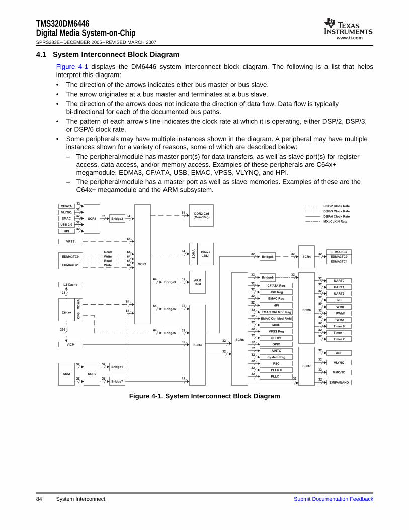
www.ti.com
4.1 System Interconnect Block Diagram
SCR5
SCR1
Bridge2
CF/ATA
VLYNQ
EMAC
USB 2.0
SCR2
Bridge1
Bridge7
ARM
C64x+
CF
GM
DM
A
L2 Cache
VICP
Bridge6
Bridge5
SCR3
VPSS
EDMA3TC1
Bridge3ARMTCM
C64x+L2/L1
SD
MA
DDR2 Ctrl(Mem/Reg)
SCR6
CF/ATA Reg
USB Reg
EMAC Reg
EMAC Ctrl Mod Reg
EMAC Ctrl Mod RAM
MDIO
VPSS Reg
SPI 0/1
GPIO
AINTC
System Reg
PSC
PLLC 0
PLLC 1
Bridge9
Bridge8
SCR7
ASP
VLYNQ
MMC/SD
EMIFA/NAND
SCR8
UART0
UART1
UART2
I2C
PWM0
PWM1
PWM2
Timer 0
Timer 1
Timer 2
SCR4
EDMA3CC
EDMA3TC0
EDMA3TC1
32
32
32
32 64
32
32
32
32
64
64
64
64
64
Read
Write
Read
Write
64
64
64
64
64
128
256
32
32
32
32
32
32
64
64
32
32
32
32
32
32
32
32
32
32
32
32
32
32
32
32
32
32
32 32
32
32
32
32
32
32
32
32
32
32
32
32
32
32
DSP/2 Clock Rate
DSP/3 Clock Rate
DSP/6 Clock Rate
EDMA3TC0
MXI/CLKIN Rate
32
32
HPI32
HPI32
TMS320DM6446Digital Media System-on-ChipSPRS283E–DECEMBER 2005–REVISED MARCH 2007
Figure 4-1 displays the DM6446 system interconnect block diagram. The following is a list that helpsinterpret this diagram:• The direction of the arrows indicates either bus master or bus slave.• The arrow originates at a bus master and terminates at a bus slave.• The direction of the arrows does not indicate the direction of data flow. Data flow is typically
bi-directional for each of the documented bus paths.• The pattern of each arrow's line indicates the clock rate at which it is operating, either DSP/2, DSP/3,
or DSP/6 clock rate.• Some peripherals may have multiple instances shown in the diagram. A peripheral may have multiple
instances shown for a variety of reasons, some of which are described below:– The peripheral/module has master port(s) for data transfers, as well as slave port(s) for register
access, data access, and/or memory access. Examples of these peripherals are C64x+megamodule, EDMA3, CF/ATA, USB, EMAC, VPSS, VLYNQ, and HPI.
– The peripheral/module has a master port as well as slave memories. Examples of these are theC64x+ megamodule and the ARM subsystem.
Figure 4-1. System Interconnect Block Diagram
84 System Interconnect Submit Documentation Feedback
www.ti.com
5 Device Operating Conditions
5.1 Absolute Maximum Ratings Over Operating Case Temperature Range
TMS320DM6446Digital Media System-on-Chip
SPRS283E–DECEMBER 2005–REVISED MARCH 2007
(Unless Otherwise Noted) (1)
Core (CVDD, VDDA1P1V, USB_VDDA1P2LDO(2), CVDDDSP) (3) -0.5 V to 1.5 V
I/O, 3.3V (DVDD33, USB_VDDA3P3) (3) -0.5 V to 4.2 VSupply voltage rangesI/O, 1.8V (DVDD18, DVDDR2, DDR_VDDDLL, PLLVDD18, VDDA1P8V, -0.5 V to 2.5 VUSB_VDD1P8, MXVDD, M24VDD) (3)
VI I/O, 3.3V -0.5 V to 4.2 VInput voltage ranges
VI I/O, 1.8V -0.5 V to 2.5 V
VO I/O, 3.3V -0.5 V to 4.2 VOutput voltage ranges
VO I/O, 1.8V -0.5 V to 2.5 V
Operating case temperature ranges, TC (default) 0°C to 85°C
Storage temperature range, Tstg (default) -55°C to 150°C
(1) Stresses beyond those listed under "absolute maximum ratings" may cause permanent damage to the device. These are stress ratingsonly, and functional operation of the device at these or any other conditions beyond those indicated under "recommended operatingconditions" is not implied. Exposure to absolute-maximum-rated conditions for extended periods may affect device reliability.
(2) This pin is an internal LDO output and connected via 1 µF capacitor to USB_VSSA1P2LDO.(3) All voltage values are with respect to VSS.
Submit Documentation Feedback Device Operating Conditions 85

www.ti.com
5.2 Recommended Operating Conditions
TMS320DM6446Digital Media System-on-ChipSPRS283E–DECEMBER 2005–REVISED MARCH 2007
MIN NOM MAX UNIT
Supply voltage, Core (CVDD, VDDA1P1V, USB_VDDA1P2LDO(1),CVDD 1.14 1.2 1.26 VCVDDDSP) (-594 devices) (2)
Supply voltage, I/O, 3.3V (DVDD33, USB_DVDDA3P3) 3.15 3.3 3.45 V
DVDD Supply voltage, I/O, 1.8V (DVDD18, DVDDR2, DDR_VDDDLL, 1.71 1.8 1.89 VPLLVDD18, VDDA1P8V, USB_VDD1P8, MXVDD, M24VDD)
Supply ground (VSS, VSSA1P8V, VSSA1P1V, DDR_VSSDLL,VSS USB_VSSREF, USB_VSS1P8, USB_VSSA3P3, USB_VSSA1P2LDO, 0 0 0 V
MXVSS(3), M24VSS
(3))
DDR_VREF DDR2 reference voltage (4) 0.49DVDDR2 0.5DVDDR2 0.51DVDDR2 V
DDR_ZP DDR2 impedance control, connected via 200 Ω resistor to VSS VSS V
DDR2 impedance control, connected via 200 Ω resistor toDDR_ZN DVDDR2 VDVDDR2
DAC_VREF DAC reference voltage input 0.475 0.5 0.525 V
DAC_RBIAS DAC biasing, connected via 4 kΩ resistor to VSSA_1P8V VSSA_1P8V V
USB_VBUS USB external charge pump input 4.75 5 5.25 V
High-level input voltage, I/O, 3.3V 2 VVIH
High-level input voltage, non-DDR I/O, 1.8V 0.65DVDD V
Low-level input voltage, I/O, 3.3V 0.8 VVIL
Low-level input voltage, non-DDR I/O, 1.8V 0.35DVDD V
TC Operating case temperature Default 0 85 °C
FSYSCLK1 DSP Operating Frequency (SYSCLK1) 20 600 MHz
(1) This pin is an internal LDO output and connected via 1 µF capacitor to USB_VSSA1P2LDO.(2) Future variants of TI SOC devices may operate at voltages ranging from 0.9 V to 1.4 V to provide a range of system power/performance
options. TI highly recommends that users design-in a supply that can handle multiple voltages within this range (i.e., 1.0 V, 1.05 V,1.1 V, 1.14 V, 1.2, 1.26 V with ±3% tolerances) by implementing simple board changes such as reference resistor values or input pinconfiguration modifications. Not incorporating a flexible supply may limit the system's ability to easily adapt to future versions of TI SOCdevices.
(3) Oscillator ground must be kept separate from other grounds and connected directly to the crystal load capacitor ground.(4) DDR_VREF is expected to equal 0.5DVDDR2 of the transmitting device and to track variations in the DVDDR2.
Device Operating Conditions86 Submit Documentation Feedback

www.ti.com
5.3 Electrical Characteristics Over Recommended Ranges of Supply Voltage and Operating
TMS320DM6446Digital Media System-on-Chip
SPRS283E–DECEMBER 2005–REVISED MARCH 2007
Case Temperature (Unless Otherwise Noted)PARAMETER TEST CONDITIONS (1) MIN TYP MAX UNIT
Low/full speed: 2.8 USB_VDDAP3 VUSB_DN and USB_DP
High speed: 360 440 mVVOH USB_DN and USB_DP
High-level output voltage (3.3V I/O) DVDD33 = MIN, IOH = MAX 2.4 V
High-level output voltage (1.8V I/O) DVDD18 = MIN, IOH = MAX DVDD - 0.45 V
Low/full speed: 0.0 0.3 VUSB_DN and USB_DP
High speed: -10 10 mVVOL USB_DN and USB_DP
Low-level output voltage (3.3V I/O) DVDD33 = MIN, IOL = MAX 0.4 V
Low-level output voltage (1.8V I/O) DVDD18 = MIN, IOL = MAX 0.45 V
VI = VSS to DVDD without opposing ±10 µAinternal resistor
VI = VSS to DVDD with opposing internalII (2) Input current 50 100 250 µApullup resistor (3)
VI = VSS to DVDD with opposing internal -250 -100 -50 µApulldown resistor (3)
IOH High-level output current All peripherals -4 mA
IOL Low-level output current All peripherals 4 mA
VO = DVDD or VSS; internal pull disabled ±20 µAIOZ
(4) I/O Off-state output currentVO = DVDD or VSS; internal pull enabled ±100 µA
Core (CVDD, VDDA1P1V, VDDA1P2LDO(5),ICDD CVDD = 1.2 V, DSP clock = 594 MHz 767 mACVDDDSP) supply current (6)
3.3V I/O (DVDD33, USB_VDDA3P3) supplyIDDD DVDD = 3.3 V, DSP clock = 594 MHz 6 mAcurrent (6)
1.8V I/O (DVDD18, DVDDR2, DDR_VDDDLL,IDDD PLLVDD18, VDDA1P8V, USB_VDD1P8, MXVDD, DVDD = 1.8 V, DSP clock = 594 MHz 102 mA
M24VDD) supply current (6)
CI Input capacitance 4 pF
Co Output capacitance 4 pF
(1) For test conditions shown as MIN, MAX, or NOM, use the appropriate value specified in the recommended operating conditions table.(2) II applies to input-only pins and bi-directional pins. For input-only pins, II indicates the input leakage current. For bi-directional pins, II
indicates the input leakage current and off-state (Hi-Z) output leakage current.(3) Applies only to pins with an internal pullup (IPU) or pulldown (IPD) resistor.(4) IOZ applies to output-only pins, indicating off-state (Hi-Z) output leakage current.(5) This pin is an internal LDO output and connected via 1 µF capacitor to USB_VSSA1P2LDO.(6) Measured under the following conditions: 60% DSP CPU utilization; ARM doing typical activity (peripheral configurations, other
housekeeping activities); DDR2 Memory Controller at 50% utilization (135 MHz), 50% writes, 32 bits, 50% bit switching; 2 MHz ASP at100% utilization; Timer0 at 100% utilization. At room temperature (25 °C) for typical process devices. The actual current draw variesacross manufacturing processes and is highly application-dependent. For more details on core and I/O activity, as well as informationrelevant to board power supply design, see the TMS320DM644x Power Consumption Summary application report (literature numberSPRAAD6).
Submit Documentation Feedback Device Operating Conditions 87

www.ti.com
6 Peripheral and Electrical Specifications
6.1 Parameter Information
6.1.1 Parameter Information Device-Specific Information
Transmission Line
4.0 pF 1.85 pF
Z0 = 50 Ω(see note)
Tester Pin Electronics Data Manual Timing Reference Point
OutputUnderTest
NOTE: The data manual provides timing at the device pin. For output timing analysis, the tester pin electronics and its transmission line effectsmust be taken into account. A transmission line with a delay of 2 ns or longer can be used to produce the desired transmission line effect.The transmission line is intended as a load only. It is not necessary to add or subtract the transmission line delay (2 ns or longer) from thedata manual timings.
42 Ω 3.5 nH
Device Pin(see note)
Input requirements in this data manual are tested with an input slew rate of < 4 Volts per nanosecond (4 V/ns) at the device pin.
Vref
Vref = VIL MAX (or VOL MAX)
Vref = VIH MIN (or VOH MIN)
TMS320DM6446Digital Media System-on-ChipSPRS283E–DECEMBER 2005–REVISED MARCH 2007
Figure 6-1. Test Load Circuit for AC Timing Measurements
The load capacitance value stated is only for characterization and measurement of AC timing signals. Thisload capacitance value does not indicate the maximum load the device is capable of driving.
6.1.1.1 Signal Transition Levels
All input and output timing parameters are referenced to Vref for both "0" and "1" logic levels. For 3.3 V I/O,Vref = 1.5 V. For 1.8 V I/O, Vref = 0.9 V.
Figure 6-2. Input and Output Voltage Reference Levels for AC Timing Measurements
All rise and fall transition timing parameters are referenced to VIL MAX and VIH MIN for input clocks,VOLMAX and VOH MIN for output clocks.
Figure 6-3. Rise and Fall Transition Time Voltage Reference Levels
88 Peripheral and Electrical Specifications Submit Documentation Feedback
www.ti.com
6.2 Recommended Clock and Control Signal Transition Behavior
6.3 Power Supplies
6.3.1 Power-Supply Sequencing
TMS320DM6446Digital Media System-on-Chip
SPRS283E–DECEMBER 2005–REVISED MARCH 2007
6.1.1.2 Timing Parameters and Board Routing Analysis
The timing parameter values specified in this data manual do not include delays by board routings. As agood board design practice, such delays must always be taken into account. Timing values may beadjusted by increasing/decreasing such delays. TI recommends utilizing the available I/O bufferinformation specification (IBIS) models to analyze the timing characteristics correctly. To properly use IBISmodels to attain accurate timing analysis for a given system, see the Using IBIS Models for TimingAnalysis application report (literature number SPRA839). If needed, external logic hardware such asbuffers may be used to compensate any timing differences.
For the DDR2 memory controller interface, it is not necessary to use the IBIS models to analyze timingcharacteristics. TI provides a PCB routing rules solution that describes the routing rules to ensure theDDR2 memory controller interface timings are met. See the Implementing DDR2 PCB Layout on theTMS320DM644x DMSoC Application Report (literature number SPRAAC5).
All clocks and control signals should transition between VIH and VIL (or between VIL and VIH) in amonotonic manner.
For more information regarding TI's power management products and suggested devices to power TIDSPs, visit www.ti.com/dsppower.
The DM6446 includes two core supplies — CVDD and CVDDDSP, as well as three I/O supplies — DVDD18,DVDDR2, and DVDD33. To ensure proper device operation, a specific power-up sequence must be followed.
The core supply power-up sequence is dependent on the DSP boot mode selected at reset. If the DSPboot mode is configured as Self-Boot mode, then both core supplies must be powered up at the sametime.
If the DSP boot mode is configured as Host-Boot, where the ARM boots the DSP, the two core suppliesmay be ramped simultaneously or powered up separately. When powered up separately, the CVDDDSPsupply must not be ramped prior to the CVDD supply. The CVDDDSP supply must be powered up before theshorting switch is closed (enabled). Prior to powering up the CVDDDSP supply, it should be left floating andnot driven to ground. Table 6-1 and Figure 6-4 describe the power-on sequence timing requirements forDSP Host-Boot mode.
To minimize the voltage difference between these two core supplies, a single regulator source must beused to power the CVDD and CVDDDSP supplies.
For more information, see Section 3.2.1, Power Considerations at Reset.
Submit Documentation Feedback Peripheral and Electrical Specifications 89

www.ti.com
CVDD
CVDDDSP
CVDD
DVDDXX
(A)
Note A: DV denotes all I/O supplies.DDXX
TMS320DM6446Digital Media System-on-ChipSPRS283E–DECEMBER 2005–REVISED MARCH 2007
Table 6-1. Core Supply Power-On Timing Requirements for DSP Host-Boot Mode (see Figure 6-4)
-594NO. UNIT
MIN MAX
1 td(CVDD-CVDDDSP) Delay time, CVDD supply ready to CVDDDSP supply ramp start 0 (1) ns
(1) In Host-Boot mode, the CVDDDSP supply must be powered up prior to closing (enabling) the shorting switch between the ALWAYS ONand DSP power domains.
Figure 6-4. DSP Host-Boot Mode Core Supply Timings
Once the CVDD supply has been powered up, the I/O supplies may be powered up. Table 6-2 andFigure 6-5 show the power-on sequence timing requirements for the Core vs. I/O power-up. DVDDXX isused to denote all I/O supplies. Note: the DVDDXX supply power-up is specified relative to the CVDD supplypower-up, not the CVDDDSP supply.
Table 6-2. I/O Supply Power-On Timing Requirements (see Figure 6-5)
-594NO. UNIT
MIN MAX
1 td(CVDD-DVDD) Delay time, CVDD supply ready to DVDDXX supply ramp start 0 100 ms
Figure 6-5. I/O Supply Timings
There is not a specific power-up sequence that must be followed with respect to the order of the power-upof the DVDD18, DVDDR2, and DVDD33 supplies. Once the CVDD supply is powered up and the td(CVDD-DVDDXX)specification is met, the DVDD18, DVDDR2, and DVDD33 supplies may be powered up in any order ofpreference. All other supplies may also be powered up in any order of preference once the td(CVDD-DVDDXX)specification has been met.
Peripheral and Electrical Specifications90 Submit Documentation Feedback

www.ti.com
TMS320DM6446Digital Media System-on-Chip
SPRS283E–DECEMBER 2005–REVISED MARCH 2007
6.3.1.1 Power-Supply Design Considerations
Core and I/O supply voltage regulators should be located close to the DSP (or DSP array) to minimizeinductance and resistance in the power delivery path. Additionally, when designing for high-performanceapplications utilizing the DM6446 device, the PC board should include separate power planes for core,I/O, and ground, all bypassed with high-quality low-ESL/ESR capacitors.
6.3.1.2 Power-Supply Decoupling
In order to properly decouple the supply planes from system noise, place as many capacitors (caps) aspossible close to DM6446. Assuming 0603 caps, the user should be able to fit a total of 60 caps, 30 forthe core supplies and 30 for the I/O supplies. These caps need to be close to the DM6446 power pins, nomore than 1.25 cm maximum distance to be effective. Physically smaller caps, such as 0402, are betterbecause of their lower parasitic inductance. Proper capacitance values are also important. Small bypasscaps (near 560 pF) should be closest to the power pins. Medium bypass caps (220 nF or as large as canbe obtained in a small package) should be next closest. TI recommends no less than 8 small and8 medium caps per supply be placed immediately next to the BGA vias, using the "interior" BGA spaceand at least the corners of the "exterior".
Larger caps for each supply can be placed further away for bulk decoupling. Large bulk caps (on the orderof 100 µF) should be furthest away, but still as close as possible. Large caps for each supply should beplaced outside of the BGA footprint.
Any cap selection needs to be evaluated from a yield/manufacturing point-of-view. As with the selection ofany component, verification of capacitor availability over the product’s production lifetime should beconsidered.
6.3.1.3 DM6446 Power and Clock Domains
DM6446 includes two separate power domains: "Always On" and "DSP". The "Always On" power domainis always on when the chip is on. The "Always On" domain is powered by the VDD pins of the DM6446.The majority of the DM6446's modules lie within the "Always On" power domain. A separate domain calledthe "DSP" domain houses the C64x+ and VICP. The "DSP" domain is not always on. The "DSP" powerdomain is powered by the CVDDDSP pins of the DM6446. Table 6-3 provides a listing of the DM6446 powerand clock domains.
Two primary reference clocks are required for the DM6446 device. These can either be crystal input ordriven by external oscillators. A 27-MHz crystal is recommended for the system PLLs, which generate theinternal clocks for the ARM, DSP, coprocessors, peripherals (including imaging peripherals), and EDMA3.The recommended 27-MHz input enables the use of the video DACs to drive NTSC/PAL television signalsat the proper frequencies. A 24-MHz crystal is also required if the USB peripheral is to be used. Forfurther description of the DM6446 clock domains, see Table 6-4 and Figure 6-6.
Submit Documentation Feedback Peripheral and Electrical Specifications 91

www.ti.com
TMS320DM6446Digital Media System-on-ChipSPRS283E–DECEMBER 2005–REVISED MARCH 2007
Table 6-3. DM6446 Power and Clock Domains
POWER DOMAIN CLOCK DOMAIN PERIPHERAL/MODULE
Always On CLKIN UART0
Always On CLKIN UART1
Always On CLKIN UART2
Always On CLKIN I2C
Always On CLKIN Timer0
Always On CLKIN Timer1
Always On CLKIN Timer2
Always On CLKIN PWM0
Always On CLKIN PWM1
Always On CLKIN PWM2
Always On CLKDIV2 ARM Subsystem
Always On CLKDIV3 DDR2
Always On CLKDIV3 VPSS
Always On CLKDIV3 EDMA
Always On CLKDIV3 SCR
Always On CLKDIV6 GPSC
Always On CLKDIV6 LPSCs
Always On CLKDIV6 Ice Pick
Always On CLKDIV6 EMIFA
Always On CLKDIV6 USB
Always On CLKDIV6 HPI
Always On CLKDIV6 VLYNQ
Always On CLKDIV6 EMAC
Always On CLKDIV6 ATA/CF
Always On CLKDIV6 MMC/SD/SDIO
Always On CLKDIV6 SPI
Always On CLKDIV6 ASP
Always On CLKDIV6 GPIO
DSP CLKDIV1 C64x+ CPU
Table 6-4. DM6446 Clock Domains (1)
CLOCK MODES (FREQUENCY)SUBSYSTEM FIXED RATIO vs. PLL1
PLL BYPASS PLL ENABLED
PLL1 – 27 MHz 594 MHz
DSP 1:1 27 MHz 594 MHz
ARM 1:2 13.5 MHz 297 MHz
EDMA3/VPSS 1:3 9 MHz 198 MHz
Peripherals 1:6 4.5 MHz 99 MHz
(1) These table values assume a MXI/CLKIN of 27 MHz and a PLL1 multiplier equal to 22.
Peripheral and Electrical Specifications92 Submit Documentation Feedback

www.ti.com
DSP Subsystem
ARM Subsystem
VICP
SYSCLK1
SYSCLK2
SYSCLK5
SCR
EDMA
VPFE
VPBE
DACs
DDR2 PHY
DDR2 VTP
DDR2 Mem Ctlr
PLLDIV1 (/1)
PLLDIV2 (/2)
BPDIV
PLL Controller 2
PLL Controller 1
PLLDIV3 (/3)
PLLDIV5 (/6)
PLLDIV2 (/2)
PLLDIV1 (/1)
SYSCLK3
Bypass ClockUARTs (x3)
I2C
Timers (x3)
PWMs (x3)
ATA/CF
EMIF/NAND
EMAC
VLYNQ
MMC/SD
SPI
GPIO
ASP
HPI
USB 2.0
USB PHY
60 MHz
24 MHz
27 MHz
PCLK
VPBECLK
PLLDIV4 (/4)
ARM INTC
TMS320DM6446Digital Media System-on-Chip
SPRS283E–DECEMBER 2005–REVISED MARCH 2007
Figure 6-6. PLL1 and PLL2 Clock Domain Block Diagram
For further detail on PLL1 and PLL2, see the structure block diagrams Figure 6-7 and Figure 6-8,respectively.
Submit Documentation Feedback Peripheral and Electrical Specifications 93

www.ti.com
PLLDIV1 (/1)
PLLDIV2 (/2)
PLLDIV4 (/4)
PLLDIV3 (/3)
PLLDIV5 (/6)
SYSCLK1
SYSCLK2
SYSCLK4
SYSCLK3
SYSCLK5
1
0
Post−DIV
PLLM
PLL0
1
BPDIV
CLKMODE
CLKIN
OSCIN
PLLEN
AUXCLK
SYSCLKBP
PLLDIV1
PLLDIV2
1
0
Post−Div(/1)
PLLM
PLL0
1
BPDIV
CLKMODE
CLKIN
OSCIN
PLLEN
PLL2_SYSCLK1(VPSS−VPBE)
PLL2_SYSCLK2(DDR2 PHY)
PLL2_SYSCLKBP(DDR2 VTP)
TMS320DM6446Digital Media System-on-ChipSPRS283E–DECEMBER 2005–REVISED MARCH 2007
Figure 6-7. PLL1 Structure Block Diagram
Figure 6-8. PLL2 Structure Block Diagram
6.3.1.4 Power and Sleep Controller (PSC) Module
The Power and Sleep Controller (PSC) controls DM6446 device power by turning off unused powerdomains or gating off clocks to individual peripherals/modules. The PSC consists of a Global PSC (GPSC)and a set of Local PSCs (LPSCs). The GPSC contains memory mapped registers, power domain control,PSC interrupt control, and a state machine for each peripheral/module. An LPSC is associated with eachperipheral/module and provides clock and reset control. The GPSC controls all of DM6446’s LPSCs. TheARM subsystem does not have an LPSC module. ARM sleep mode is accomplished through the wait forinterrupt instruction. The LPSCs for DM6446 are shown in Table 6-5. The PSC register memory map isgiven in Table 6-6. For more details on the PSC, see the Documentation Support section of theTMS320DM644x DMSoC ARM Subsystem Reference Guide (literature number SPRUE14).
Peripheral and Electrical Specifications94 Submit Documentation Feedback
www.ti.com
TMS320DM6446Digital Media System-on-Chip
SPRS283E–DECEMBER 2005–REVISED MARCH 2007
Table 6-5. DM6446 LPSC Assignments
LPSC PERIPHERAL/MODULE LPSC PERIPHERAL/MODULE LPSC PERIPHERAL/MODULENUMBER NUMBER NUMBER
0 VPSS DMA 14 EMIFA 28 TIMER1
1 VPSS MMR 15 MMC/SD/SDIO 29 Reserved
2 EDMACC 16 Reserved 30 Reserved
3 EDMATC0 17 ASP 31 Reserved
4 EDMATC1 18 I2C 32 Reserved
5 EMAC 19 UART0 33 Reserved
6 EMAC Memory Controller 20 UART1 34 Reserved
7 MDIO 21 UART2 35 Reserved
8 Reserved 22 SPI 36 Reserved
9 USB 23 PWM0 37 Reserved
10 ATA/CF 24 PWM1 38 Reserved
11 VLYNQ 25 PWM2 39 C64x+ CPU
12 HPI 26 GPIO 40 VICP
13 DDR2 Memory Controller 27 TIMER0
Table 6-6. PSC Register Memory Map
REGISTERHEX ADDRESS RANGE DESCRIPTIONACRONYM
0x01C4 1000 PID Peripheral Revision and Class Information Register
0x01C4 1003 - 0x01C4 101F - Reserved
0x01C4 1010 GBLCTL Global Control Register
0x01C4 1014 - Reserved
0x01C4 1018 INTEVAL Interrupt Evaluation Register
0x01C4 101C - 0x01C4 103F - Reserved
0x01C4 1040 MERRPR0 Module Error Pending 0 (mod 0 - 31) Register
0x01C4 1044 MERRPR1 Module Error Pending 1 (mod 32- 63) Register
0x01C4 1048 - 0x01C4 104F - Reserved
0x01C4 1050 MERRCR0 Module Error Clear 0 (mod 0 - 31) Register
0x01C4 1054 MERRCR1 Module Error Clear 1 (mod 32 - 63) Register
0x01C4 1058 - 0x01C4 105F - Reserved
0x01C4 1060 PERRPR Power Error Pending Register
0x01C4 1064 - 0x01C4 1067 - Reserved
0x01C4 1068 PERRCR Power Error Clear Register
0x01C4 106C - 0x01C4 106F - Reserved
0x01C4 1070 EPCPR External Power Error Pending Register
0x01C4 1074 - 0x01C4 1077 - Reserved
0x01C4 1078 EPCCR External Power Control Clear Register
0x01C4 107C - 0x01C4 10FF - Reserved
0x01C4 1100 RAILSTAT Power Rail Status Register
0x01C4 1104 RAILCTL Power Rail Control Register
0x01C4 1108 RAILSEL Power Rail Counter Select Register
0x01C4 110C - 0x01C4 111F - Reserved
0x01C4 1120 PTCMD Power Domain Transition Command Register
0x01C4 1124 - 0x01C4 1127 - Reserved
0x01C4 1128 PTSTAT Power Domain Transition Status Register
Submit Documentation Feedback Peripheral and Electrical Specifications 95

www.ti.com
TMS320DM6446Digital Media System-on-ChipSPRS283E–DECEMBER 2005–REVISED MARCH 2007
Table 6-6. PSC Register Memory Map (continued)
REGISTERHEX ADDRESS RANGE DESCRIPTIONACRONYM
0x01C4 112C - 0x01C4 11FF - Reserved
0x01C4 1200 PDSTAT0 Power Domain Status 0 Register (Always On)
0x01C4 1204 PDSTAT1 Power Domain Status 1 Register (DSP)
0x01C4 1208 - 0x01C4 12FF - Reserved
0x01C4 1300 PDCTL0 Power Domain Control 0 Register (Always On)
0x01C4 1304 PDCTL1 Power Domain Control 1 Register (DSP)
0x01C4 1308 - 0x01C4 150F - Reserved
0x01C4 1510 MCKOUT0 Module Clock Output Status (mod 0-31) Register
0x01C4 1514 MCKOUT1 Module Clock Output Status (mod 32-63) Register
0x01C4 1518 - 0x01C4 15FF - Reserved
0x01C4 1600 MDCFG0 Module Configuration 0 Register (VPSS DMA)
0x01C4 1604 MDCFG1 Module Configuration 1 Register (VPSS MMR)
0x01C4 1608 MDCFG2 Module Configuration 2 Register (EDMACC)
0x01C4 160C MDCFG3 Module Configuration 3 Register (EDMATC0)
0x01C4 1610 MDCFG4 Module Configuration 4 Register (EDMATC1)
0x01C4 1614 MDCFG5 Module Configuration 5 Register (EMAC)
0x01C4 1618 MDCFG6 Module Configuration 6 Register (EMAC Memory Controller)
0x01C4 161C MDCFG7 Module Configuration 7 Register (MDIO)
0x01C4 1620 Reserved
0x01C4 1624 MDCFG9 Module Configuration 9 Register (USB)
0x01C4 1628 MDCFG10 Module Configuration 10 Register (ATA/CF)
0x01C4 162C MDCFG11 Module Configuration 11 Register (VLYNQ)
0x01C4 1630 MDCFG12 Module Configuration 12 Register (HPI)
0x01C4 1634 MDCFG13 Module Configuration 13 Register (DDR2)
0x01C4 1638 MDCFG14 Module Configuration 14 Register (EMIFA)
0x01C4 163C MDCFG15 Module Configuration 15 Register (MMC/SD/SDIO)
0x01C4 1640 Reserved
0x01C4 1644 MDCFG17 Module Configuration 17 Register (ASP)
0x01C4 1648 MDCFG18 Module Configuration 18 Register (I2C)
0x01C4 164C MDCFG19 Module Configuration 19 Register (UART0)
0x01C4 1650 MDCFG20 Module Configuration 20 Register (UART1)
0x01C4 1654 MDCFG21 Module Configuration 21 Register (UART2)
0x01C4 1658 MDCFG22 Module Configuration 22 Register (SPI)
0x01C4 165C MDCFG23 Module Configuration 23 Register (PWM0)
0x01C4 1660 MDCFG24 Module Configuration 24 Register (PWM1)
0x01C4 1664 MDCFG25 Module Configuration 25 Register (PWM2)
0x01C4 1668 MDCFG26 Module Configuration 26 Register (GPIO)
0x01C4 166C MDCFG27 Module Configuration 27 Register (TIMER0)
0x01C4 1670 MDCFG28 Module Configuration 28 Register (TIMER1)
0x01C4 1674 - 0x01C4 169B - Reserved
0x01C4 169C MDCFG39 Module Configuration 39 Register (C64x+ CPU)
0x01C4 16A0 MDCFG40 Module Configuration 40 Register (VICP)
0x01C4 16A4 - 0x01C4 17FF - Reserved
0x01C4 1800 MDSTAT0 Module Status 0 Register (VPSS DMA)
0x01C4 1804 MDSTAT1 Module Status 1 Register (VPSS MMR)
0x01C4 1808 MDSTAT2 Module Status 2 Register (EDMACC)
Peripheral and Electrical Specifications96 Submit Documentation Feedback

www.ti.com
TMS320DM6446Digital Media System-on-Chip
SPRS283E–DECEMBER 2005–REVISED MARCH 2007
Table 6-6. PSC Register Memory Map (continued)
REGISTERHEX ADDRESS RANGE DESCRIPTIONACRONYM
0x01C4 180C MDSTAT3 Module Status 3 Register (EDMATC0)
0x01C4 1810 MDSTAT4 Module Status 4 Register (EDMATC1)
0x01C4 1814 MDSTAT5 Module Status 5 Register (EMAC)
0x01C4 1818 MDSTAT6 Module Status 6 Register (EMAC Memory Controller)
0x01C4 181C MDSTAT7 Module Status 7 Register (MDIO)
0x01C4 1820 Reserved
0x01C4 1824 MDSTAT9 Module Status 9 Register (USB)
0x01C4 1828 MDSTAT10 Module Status 10 Register (ATA/CF)
0x01C4 182C MDSTAT11 Module Status 11 Register (VLYNQ)
0x01C4 1830 MDSTAT12 Module Status 12 Register (HPI)
0x01C4 1834 MDSTAT13 Module Status 13 Register (DDR2)
0x01C4 1838 MDSTAT14 Module Status 14 Register (EMIFA)
0x01C4 183C MDSTAT15 Module Status 15 Register (MMC/SD/SDIO)
0x01C4 1840 Reserved
0x01C4 1844 MDSTAT17 Module Status 17 Register (ASP)
0x01C4 1848 MDSTAT18 Module Status 18 Register (I2C)
0x01C4 184C MDSTAT19 Module Status 19 Register (UART0)
0x01C4 1850 MDSTAT20 Module Status 20 Register (UART1)
0x01C4 1854 MDSTAT21 Module Status 21 Register (UART2)
0x01C4 1858 MDSTAT22 Module Status 22 Register (SPI)
0x01C4 185C MDSTAT23 Module Status 23 Register (PWM0)
0x01C4 1860 MDSTAT24 Module Status 24 Register (PWM1)
0x01C4 1864 MDSTAT25 Module Status 25 Register (PWM2)
0x01C4 1868 MDSTAT26 Module Status 26 Register (GPIO)
0x01C4 186C MDSTAT27 Module Status 27 Register (TIMER0)
0x01C4 1870 MDSTAT28 Module Status 28 Register (TIMER1)
0x01C4 1874 - 0x01C4 189B - Reserved
0x01C4 189C MDSTAT39 Module Status 39 Register (C64x+ CPU)
0x01C4 18A0 MDSTAT40 Module Status 40 Register (VICP)
0x01C4 18A4 - 0x01C4 19FF - Reserved
0x01C4 1A00 MDCTL0 Module Control 0 Register (VPSS DMA)
0x01C4 1A04 MDCTL1 Module Control 1 Register (VPSS MMR)
0x01C4 1A08 MDCTL2 Module Control 2 Register (EDMACC)
0x01C4 1A0C MDCTL3 Module Control 3 Register (EDMATC0)
0x01C4 1A10 MDCTL4 Module Control 4 Register (EDMATC1)
0x01C4 1A14 MDCTL5 Module Control 5 Register (EMAC)
0x01C4 1A18 MDCTL6 Module Control 6 Register (EMAC Memory Controller)
0x01C4 1A1C MDCTL7 Module Control 7 Register (MDIO)
0x01C4 1A20 Reserved
0x01C4 1A24 MDCTL9 Module Control 9 Register (USB)
0x01C4 1A28 MDCTL10 Module Control 10 Register (ATA/CF)
0x01C4 1A2C MDCTL11 Module Control 11 Register (VLYNQ)
0x01C4 1A30 MDCTL12 Module Control 12 Register (HPI)
0x01C4 1A34 MDCTL13 Module Control 13 Register (DDR2)
0x01C4 1A38 MDCTL14 Module Control 14 Register (EMIFA)
0x01C4 1A3C MDCTL15 Module Control 15 Register (MMC/SD/SDIO)
Submit Documentation Feedback Peripheral and Electrical Specifications 97

www.ti.com
6.4 Reset
TMS320DM6446Digital Media System-on-ChipSPRS283E–DECEMBER 2005–REVISED MARCH 2007
Table 6-6. PSC Register Memory Map (continued)
REGISTERHEX ADDRESS RANGE DESCRIPTIONACRONYM
0x01C4 1A40 Reserved
0x01C4 1A44 MDCTL17 Module Control 17 Register (ASP)
0x01C4 1A48 MDCTL18 Module Control 18 Register (I2C)
0x01C4 1A4C MDCTL19 Module Control 19 Register (UART0)
0x01C4 1A50 MDCTL20 Module Control 20 Register (UART1)
0x01C4 1A54 MDCTL21 Module Control 21 Register (UART2)
0x01C4 1A58 MDCTL22 Module Control 22 Register (SPI)
0x01C4 1A5C MDCTL23 Module Control 23 Register (PWM0)
0x01C4 1A60 MDCTL24 Module Control 24 Register (PWM1)
0x01C4 1A64 MDCTL25 Module Control 25 Register (PWM2)
0x01C4 1A68 MDCTL26 Module Control 26 Register (GPIO)
0x01C4 1A6C MDCTL27 Module Control 27 Register (TIMER0)
0x01C4 1A70 MDCTL28 Module Control 28 Register (TIMER1)
0x01C4 1A74 - 0x01C4 1A9B - Reserved
0x01C4 1A9C MDCTL39 Module Control 39 Register (C64x+ CPU)
0x01C4 1AA0 MDCTL40 Module Control 40 Register (VICP)
0x01C4 1AA4 - 0x01C4 1FFF - Reserved
0x01C4 1000 MPFAR Memory Protection Fault Address Register
0x01C4 1004 MPFSR Memory Protection Fault Status Register
0x01C4 1008 MPFCR Memory Protection Fault Command Register
0x01C4 100C MPAA Memory Protection Page Attribute Register
0x01C4 1010 - 0x01C4 1FFF - Reserved
DM6446 supports various types of resets. Power-on-reset (POR), warm reset, max reset, system reset,C64x+ local reset, and module reset are summarized in Table 6-7.
Table 6-7. DM6446 Resets
Type Initiator Description
Power-on-reset (POR) RESET pin active low while TRST is low. Global chip reset (Cold reset). Activates the POR signalon chip, which is used to reset test and emulation logic.
Warm reset RESET pin active low while TRST is high. Resets everything except for test and emulation logic.ARM emulator stays alive during warm reset, but theC64x+ emulator does not.
Maximum reset Emulator, WD Timer Same as Warm reset, except for initiators.
C64x+ Local reset Software (register bit) MMR controls the C64x+ reset input. This is used forcontrol of C64x+ reset by the ARM. The C64x+ SlaveDMA port is still alive when in local reset.
Power-on-reset (POR) is the global chip reset and it affects test, emulation, and other circuitry. It isinvoked by driving the RESET pin active low while TRST is held low. A POR is required to place DM6446into a known good initial state. POR can be asserted prior to ramping the core and I/O voltages or afterthe core and I/O voltages have reached their proper operating conditions. As a best practice, RESETshould be asserted (held low) during power-up. Prior to deasserting RESET (low-to-high transition), thecore and I/O voltages should be at their proper operating conditions and if an external 27 MHz oscillator isused on the MXI/CLKIN pin, the external clock should also be running at the correct frequency.
Peripheral and Electrical Specifications98 Submit Documentation Feedback
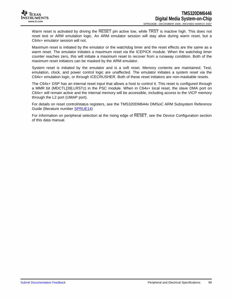
www.ti.com
TMS320DM6446Digital Media System-on-Chip
SPRS283E–DECEMBER 2005–REVISED MARCH 2007
Warm reset is activated by driving the RESET pin active low, while TRST is inactive high. This does notreset test or ARM emulation logic. An ARM emulator session will stay alive during warm reset, but aC64x+ emulator session will not.
Maximum reset is initiated by the emulator or the watchdog timer and the reset effects are the same as awarm reset. The emulator initiates a maximum reset via the ICEPICK module. When the watchdog timercounter reaches zero, this will initiate a maximum reset to recover from a runaway condition. Both of themaximum reset initiators can be masked by the ARM emulator.
System reset is initiated by the emulator and is a soft reset. Memory contents are maintained. Test,emulation, clock, and power control logic are unaffected. The emulator initiates a system reset via theC64x+ emulation logic, or through ICECRUSHER. Both of these reset initiators are non-maskable resets.
The C64x+ DSP has an internal reset input that allows a host to control it. This reset is configured througha MMR bit (MDCTL[39].LRSTz) in the PSC module. When in C64x+ local reset, the slave DMA port onC64x+ will remain active and the internal memory will be accessible, including access to the VICP memorythrough the L2 port (UMAP port).
For details on reset control/status registers, see the TMS320DM644x DMSoC ARM Subsystem ReferenceGuide (literature number SPRUE14)
For information on peripheral selection at the rising edge of RESET, see the Device Configuration sectionof this data manual.
Submit Documentation Feedback Peripheral and Electrical Specifications 99

www.ti.com
6.4.1 Reset Electrical Data/Timing
TMS320DM6446Digital Media System-on-ChipSPRS283E–DECEMBER 2005–REVISED MARCH 2007
Table 6-8. Timing Requirements for Reset (see Figure 6-9)
-594NO. UNIT
MIN MAX
1 tw(RST) Width of the RESET pulse 444 ns
2 tsu(BOOT) Setup time, boot configuration bits valid before RESET high 444 ns
3 th(BOOT) Hold time, boot configuration bits valid after RESET high 444 ns
Table 6-9. Switching Characteristics Over Recommended Operating Conditions During Reset (1)
(see Figure 6-9)
-594NO. UNIT
MIN MAX
26 td(PLL_LOCK) Delay time, PLL1 lock time 2000P ns
4 td(RSTL-DDRZZ) Delay time, RESET low to DDR2 Z Group high impedance 0 2P + 20 ns
5 td(RSTL-DDRLL) Delay time, RESET low to DDR2 Low Group low 0 20 ns
6 td(RSTL-DDRHH) Delay time, RESET low to DDR2 High Group high 0 20 ns
16 td(RSTL-DDRZHZ) Delay time, RESET low to DDR2 Z/High Group high impedance 0 5P + 20 ns
17 td(RSTL-DDRLHL) Delay time, RESET low to DDR2 Low/High Group low 0 20 ns
7 td(RSTL-ZZ) Delay time, RESET low to Z Group high impedance 0 20 ns
8 td(RSTL-LOWL) Delay time, RESET low to Low Group low 0 20 ns
9 td(RSTL-HIGHH) Delay time, RESET low to High Group high 0 20 ns
18 td(RSTL-HIGHLOWH) Delay time, RESET low to High/Low Group high 0 20 ns
19 td(RSTL-LOWHIGHL) Delay time, RESET low to Low/High Group low 0 20 ns
24 td(RSTL-ZIZ) Delay time, RESET low to Z/Invalid Group high impedance 0 20 ns
10 td(RSTH-DDRZV) Delay time, RESET high to DDR2 Z Group valid (2) ns
11 td(RSTH-DDRLV) Delay time, RESET high to DDR2 Low Group valid (2) ns
12 td(RSTH-DDRHV) Delay time, RESET high to DDR2 High Group valid (2) ns
20 td(RSTH-DDRZHV) Delay time, RESET high to DDR2 Z/High Group valid high 4000P ns
21 td(RSTH-DDRLHV) Delay time, RESET high to DDR2 Low/High Group valid high 4000P ns
13 td(RSTH-ZV) Delay time, RESET high to Z Group valid (2) ns
14 td(RSTH-LOWV) Delay time, RESET high to Low Group valid (2) ns
15 td(RSTH-HIGHV) Delay time, RESET high to High Group valid (2) ns
22 td(RSTH-HIGHLOWV) Delay time, RESET high to High/Low Group valid low 5100P ns
23 td(RSTH-LOWHIGHV) Delay time, RESET high to Low/High Group valid high 5100P ns
25 td(RSTH-ZIIV) Delay time, RESET high to Z/Invalid Group invalid 4000P ns
(1) P = MXI/CLKIN cycle time, in ns.(2) Following RESET high, this signal group maintains the state the pins(s) achieved while RESET was driven low until the peripheral is
enabled via the PSC. For example, the DDR2 Z Group goes high impedance following RESET low and remains in the high-impedancestate following RESET high until the DDR2 controller is enabled via the PSC.
Peripheral and Electrical Specifications100 Submit Documentation Feedback

www.ti.com
3
4
1RESET
BootConfiguration Pins
2
10
115DDR2 Low Group (A)
DDR2 Z Group (A)
126DDR2 High Group (A)
16 20
2117DDR2 Low/High Group (A)
DDR2 Z/High Group (A)
A. DDR2 Z Group: DDR_DQS[3:0], DDR_D[12:0]DDR2 Low Group: DDR_CLK0, DDR_CKE, DDR_A[12:0]DDR2 High Group: DDR_CLK0, DDR_CS, DDR_WE, DDR_RAS, DDR_CASDDR2 Z/High Group: DDR_DQM[3:0],DDR2 Low/High Group: DDR_BS[2:0]Low Group: DMARQ/UART_RXD1, VCLK, RTCK, TDO, VPBECLK, YOUT0/G5/AEAW0, YOUT1/G6/AEAW1,YOUT2/G7/AEAW2, YOUT3/R3/AEAW3, YOUT4/R4/AEAW4, COUT3/B6/DSP_BT, COUT2/B5/EM_WIDTH,COUT1/B4/BTSEL1, COUT0/B3/BTSEL0, TRSTHigh Group: DMACK/UART_TXD1, EM_A[2]/(CLE), EM_A[1]/(ALE), EM_CS3, EM_WE/(WE)(IOWR)/DIOWZ Group: All other pins not listed above, with the exception of power and ground pins.
The following Z Group pins have an internal pullup (IPU): DMARQ/UART_RXD1, VPBECLK, HSYNC, VSYNC,YOUT0/G5/AEAW0, YOUT1/G6/AEAW1, YOUT2/G7/AEAW2, YOUT3/R3/AEAW3, YOUT4/R4/AEAW4,COUT3/B6/DSP_BT, COUT2/B5/EM_WIDTH, COUT1/B4/BTSEL1, COUT0/B3/BTSEL0, TRST, YI/CCD[7:0],CI[3:0]/CCD[11:8], CI4/CCD12/UART_RTS2, CI5/CCD13/UART_CTS2, CI6/CCD14/UART_TXD2,CI7/CCD15/UART_RXD2
The following Z Group pins have an internal pulldown (IPD): EM_WAIT/IORDY, TCK, TDI, TMS, EMU[1:0]
High/Low Group: EM_BA[0]/DA0, EM_CS2, EM_OE/(RE)/(IORD)/DIORLow/High Group: EM_R/W/INTRQZ/Invalid Group: EM_D[15:0]
7
148Low Group (A)
Z Group (A)
159High Group (A)
13
2218High/Low Group (A)
2319Low/High Group (A)
24Z/Invalid Group (A)
25
TMS320DM6446Digital Media System-on-Chip
SPRS283E–DECEMBER 2005–REVISED MARCH 2007
Figure 6-9. Reset Timing
Submit Documentation Feedback Peripheral and Electrical Specifications 101

www.ti.com
6.5 External Clock Input From MXI/CLKIN Pin
6.5.1 Clock Input Option 1 – Crystal
MXI/CLKIN MXO
C1 C2
Crystal
MXVSS
27 MHz
1.8 V
MXVDD
RBIAS(optional)
CLC1C2
(C1 C2)
TMS320DM6446Digital Media System-on-ChipSPRS283E–DECEMBER 2005–REVISED MARCH 2007
The DM6446 device has two input pins for an external clock source, MXI/CLKIN and M24XI. TheMXI/CLKIN pin provides the clock source for PLL1 and PLL2 whose optimal frequency is 27 MHz. TheM24XI pin provides the clock source for the USB PLL whose optimal frequency is 24 MHz.
The DM6446 device includes two options to provide an external clock input:
1. Use an on-chip oscillator with external crystal or ceramic resonator circuit (only supportingparallel-resonant mode; it does not provide overtone support). For more details, see Section 6.5.1.
2. Use an external 1.8-V LVCMOS-compatible clock input. For more details, see Section 6.5.2.
6.5.1.1 27-MHz Crystal for System Oscillator
In this option, a crystal is used as the external clock input to the DM6446 PLL1 and PLL2.
The 27-MHz oscillator provides the reference clock for all DM6446 subsystems and peripherals. Theon-chip oscillator requires an external 27-MHz crystal connected across the MXI and MXO pins, alongwith two load capacitors, as shown in Figure 6-10. The external crystal load capacitors must beconnected only to the 27-MHz oscillator ground pin (MXVSS). Do not connect to board ground (VSS). TheMXVDD pin can be connected to the same 1.8 V power supply as DVDD18.
Figure 6-10. 27-MHz System Oscillator
The RBIAS resistor is optional. If the RBIAS resistor is used, it should equal 1 MΩ± 5%. The loadcapacitors, C1 and C2, should be chosen such that the equation is satisfied (typical values are C1 = C2 =10 pF). CL in the equation is the load specified by the crystal manufacturer. All discrete components usedto implement the oscillator circuit should be placed as close as possible to the associated oscillator pins(MXI and MXO) and to the MXVSS pin.
Table 6-10. Crystal Requirements for a 27-MHz System Oscillator
PARAMETER MIN TYP MAX UNIT
Start-up time (from power up until oscillating at stable frequency of 27 MHz) 4 ms
Oscillation frequency 27 MHz
ESR 60 Ω
Frequency stability ±50 ppm
Peripheral and Electrical Specifications102 Submit Documentation Feedback

www.ti.com
M24XI M24XO M24VSS M24VDD
C1 C2
Crystal24 MHz
1.8 V
RBIAS(optional)
CLC1C2
(C1 C2)
TMS320DM6446Digital Media System-on-Chip
SPRS283E–DECEMBER 2005–REVISED MARCH 2007
6.5.1.2 24-MHz Crystal for USB Oscillator
In this option, a crystal is used as the external clock input to the DM6446 USB PLL.
The 24-MHz oscillator provides the reference clock for the DM6446 USB peripheral. The on-chip oscillatorrequires an external 24-MHz crystal connected across the M24XI and M24XO pins, along with two loadcapacitors, as shown in Figure 6-11.The external crystal load capacitors must be connected only to the24-MHz oscillator ground pin (M24VSS). Do not connect to board ground (VSS).
Figure 6-11. 24-MHz USB Oscillator
The RBIAS resistor is optional. If the RBIAS resistor is used, it should equal 1 MΩ± 5%. The loadcapacitors, C1 and C2, should be chosen such that the equation is satisfied (typical values are C1 = C2 =10 pF). CL in the equation is the load specified by the crystal manufacturer. All discrete components usedto implement the oscillator circuit should be placed as close as possible to the associated oscillator pins(M24XI and M24XO) and to the M24XVSS pin.
Table 6-11. Crystal Requirements for a 24-MHz USB Oscillator
PARAMETER MIN TYP MAX UNIT
Start-up time (from power up until oscillating at stable frequency of 24 MHz) 4 ms
Oscillation frequency 24 MHz
ESR 60 Ω
Frequency stability ±50 ppm
Submit Documentation Feedback Peripheral and Electrical Specifications 103

www.ti.com
6.5.2 Clock Input Option 2 – 1.8-V LVCMOS-Compatible Clock Input
MXI/CLKIN MXO
NC
MXVSS
1.8 V
MXVDD
TMS320DM6446Digital Media System-on-ChipSPRS283E–DECEMBER 2005–REVISED MARCH 2007
In this option, a 1.8-V LVCMOS-compatible clock input is used as the external clock input to the DM6446device. The external connections are shown in Figure 6-12. The MXI/CLKIN pin is connected to the 1.8-VLVCMOS-compatible clock source. The MXO pin is left unconnected. The MXVSS pin is connected toboard ground (VSS). The MXVDD pin can be connected to the same 1.8-V power supply as DVDD18. Theclock source must meet the MXI/CLKIN timing requirements shown in Table 6-16, Timing Requirementsfor MXI/CLKIN.
Figure 6-12. 1.8-V LVCMOS-Compatible Clock Input
Figure 6-12 also applies to the USB external clock input. When a 1.8-V LVCMOS-compatible clock input isused as the external clock input, the M24XI pin is connected to the 1.8-V LVCMOS-compatible clocksource. The M24XO pin is left unconnected. The M24VSS pin is connected to board ground (VSS). TheM24VDD pin can be connected to the same 1.8-V power supply as DVDDR2. The clock source must meetthe MXI/CLKIN timing requirements shown in Table 6-17, Timing Requirements for M24XI.
Peripheral and Electrical Specifications104 Submit Documentation Feedback

www.ti.com
6.6 Clock PLLs
TMS320DM6446Digital Media System-on-Chip
SPRS283E–DECEMBER 2005–REVISED MARCH 2007
There are two independently controlled PLLs on DM6446. PLL1 generates the frequencies required for theDSP, ARM, VICP, DMA, VPFE, and other peripherals. PLL2 generates the frequencies required for theDDR2 interface and the VPBE in certain modes. The recommended reference clock for both PLLs is the27-MHz crystal input. The USB2.0 PHY contains a third PLL embedded within it and the 24-MHz oscillatoris its reference clock source. This particular PLL is only usable for USB operation, and is discussed furtherin the TMS320DM644x DMSoC Univeral Serial Bus (USB) Controller User's Guide (literature numberSPRUE35).
A summary of the PLL controller registers is shown in Table 6-12. For more details, see theTMS320DM644x DMSoC ARM Subsystem Reference Guide (literature number SPRUE14).
Table 6-12. PLL and Reset Controller Registers Memory Map
HEX ADDRESS RANGE REGISTER ACRONYM DESCRIPTION
PLL1 Controller Registers
0x01C4 0800 PID Peripheral Identification and Revision Information Register
0x01C4 08E4 RSTYPE Reset Type Register
0x01C4 0900 PLLC PLL Controller 1 Operations Control Register
0x01C4 0910 PLLM PLL Controller 1 Multiplier Control Register
0x01C4 0918 PLLDIV1 PLL Controller 1 Control-Divider 1 Register (SYSCLK1)
0x01C4 091C PLLDIV2 PLL Controller 1 Control-Divider 2 Register (SYSCLK2)
0x01C4 0920 PLLDIV3 PLL Controller 1 Control-Divider 3 Register (SYSCLK3)
0x01C4 0928 POSTDIV PLL Controller 1 Post-Divider Control Register
0x01C4 092C BPDIV PLL Controller 1 Bypass Control-Divider Register (SYSCLKBP)
0x01C4 0938 PLLCMD PLL Controller 1 Command Register
0x01C4 093C PLLSTAT PLL Controller 1 Status Register (Shows PLLCTRL Status)
PLL Controller 1 Alignment Control Register0x01C4 0940 ALNCTL (Indicates Which SYSCLKs Need to be Aligned for Proper Device Operation)
PLL Controller 1 Divider Change Register0x01C4 0944 DCHANGE (Indicates if SYSCLK Divide Ratio has Been Modified)
0x01C4 0948 CKEN PLL Controller 1 Clock Enable Register
0x01C4 094C CKSTAT PLL Controller 1 Clock Status Register (For All Clocks Except SYSCLKx)
0x01C4 0950 PLL Controller 1 System Clock Status 1 Register (Indicates SYSCLK on/offSYSTAT Status)
0x01C4 0960 PLLDIV4 PLL Controller 1 Control-Divider 4 Register (SYSCLK4)
0x01C4 0964 PLLDIV5 PLL Controller 1 Control-Divider 5 Register (SYSCLK5)
0x01C4 0C00 PID Peripheral Identification and Revision Information Register
0x01C4 0D00 PLLC PLL Controller 2 Operations Control Register
0x01C4 0D10 PLLM PLL Controller 2 Multiplier Control Register
0x01C4 0D18 PLLDIV1 PLL Controller 2 Control-Divider 1 Register (SYSCLK1)
0x01C4 0D1C PLLDIV2 PLL Controller 2 Control-Divider 2 Register (SYSCLK2)
0x01C4 0D20 - 0x01C4 0D2B POSTDIV PLL Controller 2 Post-Divider Control Register
0x01C4 0D2C BPDIV PLL Controller 2 Bypass Control-Divider Register (SYSCLKBP)
0x01C4 0D38 PLLCMD PLL Controller 2 Command Register
0x01C4 0D3C PLLSTAT PLL Controller 2 Status Register (Shows PLLCTRL Status)
PLL Controller 2 Alignment Control Register0x01C4 0D40 ALNCTL (Indicates Which SYSCLKs Need to be Aligned for Proper Device Operation)
PLL Controller 2 Divider Change Register0x01C4 0D44 DCHANGE (Indicates if SYSCLK Divide Ratio has Been Modified)
0x01C4 0D48 CKEN PLL Controller 2 Clock Enable Register
0x01C4 0D4C CKSTAT PLL Controller 2 Clock Status Register (For All Clocks Except SYSCLKx)
Submit Documentation Feedback Peripheral and Electrical Specifications 105

www.ti.com
6.6.1 PLL1 and PLL2
PLLVDD18
C2C1
EMI Filter
+1.8 V
DM644x
PLL2
PLL1
0.1 µF 0.01 µF
TMS320DM6446Digital Media System-on-ChipSPRS283E–DECEMBER 2005–REVISED MARCH 2007
Table 6-12. PLL and Reset Controller Registers Memory Map (continued)
HEX ADDRESS RANGE REGISTER ACRONYM DESCRIPTION
0x01C4 0D50 SYSTAT PLL Controller 2 System Clock Status 1 Register (Indicates SYSCLK on/offStatus)
Both PLL1 and PLL2 power is supplied externally via the 1.8 V PLL power-supply pin (PLLVDD18). It isrecommended that an external EMI filter circuit be added to PLLVDD18, as shown in Figure 6-13. The 1.8-Vsupply of the EMI filter must be from the same 1.8-V power plane supplying the device’s 1.8-V I/Opower-supply pins (DVDD). TI recommends EMI filter manufacturer Murata, part numberNFM18CC222R1C3.
All PLL external components (C1, C2, and the EMI Filter) should be placed as close to the device aspossible. For the best performance, TI recommends that all the PLL external components be on a singleside of the board without jumpers, switches, or components other than the ones shown in Figure 6-13. Forreduced PLL jitter, maximize the spacing between switching signals and the PLL external components(C1, C2, and the EMI Filter).
Figure 6-13. PLL1 and PLL2 External Connection
The minimum CLKIN rise and fall times should also be observed. For the input clock timing requirements,see Section 6.6.3, Clock PLL Electrical Data/Timing (Input and Output Clocks).
There is an allowable range for PLL multiplier (PLLM). There is a minimum and maximum operatingfrequency for MXI/CLKIN, PLLOUT, and the device clocks (SYSCLKs). The PLL Controllers must beconfigured not to exceed any of these constraints documented in this section (certain combinations ofexternal clock inputs, internal dividers, and PLL multiply ratios might not be supported).
106 Peripheral and Electrical Specifications Submit Documentation Feedback

www.ti.com
6.6.2 Clock PLL Considerations with External Clock Sources
TMS320DM6446Digital Media System-on-Chip
SPRS283E–DECEMBER 2005–REVISED MARCH 2007
Table 6-13. PLLC1 Clock Frequency Ranges
CLOCK SIGNAL NAME MIN MAX UNIT
MXI/CLKIN (1) 20 30 MHz
PLLOUT At 1.2-V CVDD 400 600 MHz
SYSCLK1 (CLKDIV1 Domain) 600 MHz
(1) MXI/CLKIN input clock is used for both PLL Controllers (PLLC1 and PLLC2).
Table 6-14. PLLC2 Clock Frequency Ranges
CLOCK SIGNAL NAME MIN MAX UNIT
MXI/CLKIN (1) 20 30 MHz
PLLOUT At 1.2-V CVDD 400 900 MHz
(1) MXI/CLKIN input clock is used for both PLL Controllers (PLLC1 and PLLC2).
Both PLL1 and PLL2 have stabilization, lock, and reset timing requirements that must be followed.
The PLL stabilization time is the amount of time that must be allotted for the internal PLL regulators tobecome stable after the PLL is powered up (after PLLCTL.PLLPWRDN bit goes through a 1-to-0transition). The PLL should not be operated until this stabilization time has expired. This stabilization stepmust be applied after these resets—a Power-on Reset, a Warm Reset, or a Max Reset, as thePLLCTL.PLLPWRDN bit resets to a "1". For the PLL stabliziation time value, see Table 6-15.
The PLL reset time is the amount of wait time needed for the PLL to properly reset (writing PLLRST = 0)before bringing the PLL out of reset (writing PLLRST = 1). For the PLL reset time value, see Table 6-15.
The PLL lock time is the amount of time needed from when the PLL is taken out of reset (PLLRST = 1with PLLEN = 0) to when to when the PLL controller can be switched to PLL mode (PLLEN = 1). For thePLL lock time value, see Table 6-15.
Table 6-15. PLL1 and PLL2 Stabilization, Lock, and Reset Times
PLL STABILIZATION/LOCK/RESET TIME MIN TYP MAX UNIT
PLL Stabilization Time 150 µs
PLL Lock Time 2000C (1) ns
PLL Reset Time 128C (1) ns
(1) C = CLKIN cycle time in ns. For example, when MXI/CLKIN frequency is 27 MHz, use C = 37.037 ns.
For details on the PLL initialization software sequence, see the TMS320DM6446 DMSoC ARM SubsystemReference Guide (literature number SPRUE14).
If the internal oscillator is bypassed, to minimize the clock jitter a single clean power supply should powerboth the DM6446 device and the external clock oscillator circuit. The minimum CLKIN rise and fall timesshould also be observed. For the input clock timing requirements, see Section 6.6.3, Clock PLL ElectricalData/Timing (Input and Output Clocks).
Rise/fall times, duty cycles (high/low pulse durations), and the load capacitance of the external clocksource must meet the device requirements in this data manual (see Section 5.3, Electrical CharacteristicsOver Recommended Ranges of Supply Voltage and Operating Case Temperature and Section 6.6.3,Clock PLL Electrical Data/Timing (Input and Output Clocks).
Submit Documentation Feedback Peripheral and Electrical Specifications 107

www.ti.com
6.6.3 Clock PLL Electrical Data/Timing (Input and Output Clocks)
MXI/CLKIN
2
3
4
4
5 1
TMS320DM6446Digital Media System-on-ChipSPRS283E–DECEMBER 2005–REVISED MARCH 2007
Table 6-16. Timing Requirements for MXI/CLKIN (-594) Devices (1) (2) (3) (4) (see Figure 6-14)
-594NO. UNIT
MIN MAX
1 tc(MXI) Cycle time, MXI/CLKIN 33.3 50 ns
2 tw(MXIH) Pulse duration, MXI/CLKIN high 0.45C 0.55C ns
3 tw(MXIL) Pulse duration, MXI/CLKIN low 0.45C 0.55C ns
4 tt(MXI) Transition time, MXI/CLKIN 0.05C ns
5 tJ(MXI) Period jitter, MXI/CLKIN 0.02C ns
(1) The MXI/CLKIN frequency and PLL multiply factor should be chosen such that the resulting clock frequency is within the specific rangefor CPU operating frequency. For example, for a -594 speed device with a 27 MHz CLKIN frequency, the PLL multiply factor should be≤ 22.
(2) The reference points for the rise and fall transitions are measured at VIL MAX and VIH MIN.(3) For more details on the PLL multiplier factors, see the Documentation Support section for ARM Subsystem User's Guide.(4) C = CLKIN cycle time in ns. For example, when MXI/CLKIN frequency is 27 MHz, use C = 37.037 ns.
Figure 6-14. MXI/CLKIN Timing
108 Peripheral and Electrical Specifications Submit Documentation Feedback

www.ti.com
MXI/CLKIN
2
3
4
4
5 1
TMS320DM6446Digital Media System-on-Chip
SPRS283E–DECEMBER 2005–REVISED MARCH 2007
Table 6-17. Timing Requirements for M24XI (-594) Devices (1) (2) (3) (see Figure 6-15)
NO. -594 UNIT
MIN TYP MAX
1 tc(M24XI) Cycle time, M24XI 41.6 ns
2 tw(M24XIH) Pulse duration, M24XI high 0.45C 0.55C ns
3 tw(M24XIL) Pulse duration, M24XI low 0.45C 0.55C ns
4 tt(M24XI) Transition time, M24XI 0.05C ns
5 tJ(M24XI) Period jitter, M24XI 0.02C ns
(1) The reference points for the rise and fall transitions are measured at VIL MAX and VIH MIN.(2) For more details on the PLL, see the Documentation Support section for USB Peripheral Reference Guide.(3) C = M24XI cycle time in ns. For example, when M24XI frequency is 24 MHz, use C = 41.6 ns.
Figure 6-15. M24XI Timing
Submit Documentation Feedback Peripheral and Electrical Specifications 109
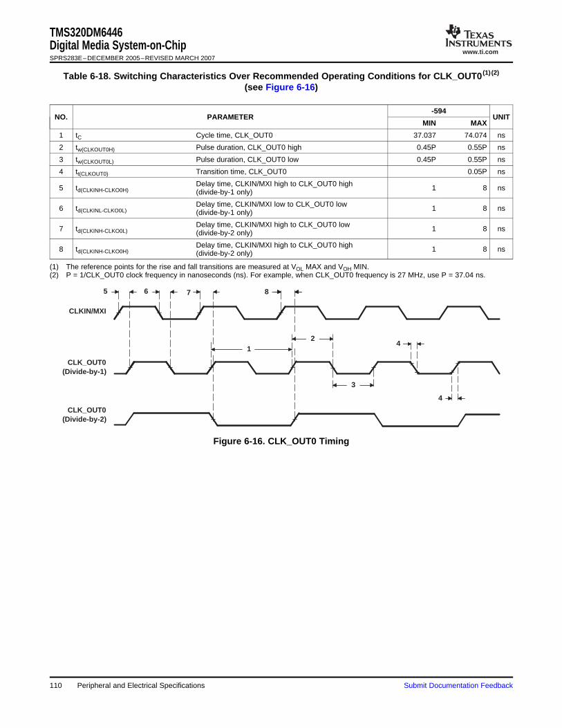
www.ti.com
CLK_OUT0(Divide-by-1)
12
4
4
CLKIN/MXI
CLK_OUT0(Divide-by-2)
5 6 7 8
3
TMS320DM6446Digital Media System-on-ChipSPRS283E–DECEMBER 2005–REVISED MARCH 2007
Table 6-18. Switching Characteristics Over Recommended Operating Conditions for CLK_OUT0 (1) (2)
(see Figure 6-16)
-594NO. PARAMETER UNIT
MIN MAX
1 tC Cycle time, CLK_OUT0 37.037 74.074 ns
2 tw(CLKOUT0H) Pulse duration, CLK_OUT0 high 0.45P 0.55P ns
3 tw(CLKOUT0L) Pulse duration, CLK_OUT0 low 0.45P 0.55P ns
4 tt(CLKOUT0) Transition time, CLK_OUT0 0.05P ns
Delay time, CLKIN/MXI high to CLK_OUT0 high5 td(CLKINH-CLKO0H) 1 8 ns(divide-by-1 only)
Delay time, CLKIN/MXI low to CLK_OUT0 low6 td(CLKINL-CLKO0L) 1 8 ns(divide-by-1 only)
Delay time, CLKIN/MXI high to CLK_OUT0 low7 td(CLKINH-CLKO0L) 1 8 ns(divide-by-2 only)
Delay time, CLKIN/MXI high to CLK_OUT0 high8 td(CLKINH-CLKO0H) 1 8 ns(divide-by-2 only)
(1) The reference points for the rise and fall transitions are measured at VOL MAX and VOH MIN.(2) P = 1/CLK_OUT0 clock frequency in nanoseconds (ns). For example, when CLK_OUT0 frequency is 27 MHz, use P = 37.04 ns.
Figure 6-16. CLK_OUT0 Timing
Peripheral and Electrical Specifications110 Submit Documentation Feedback

www.ti.com
CLK_OUT1(Divide-by-1)
12
4
4
CLKIN/MXI
CLK_OUT1(Divide-by-2)
5 6 7 8
3
TMS320DM6446Digital Media System-on-Chip
SPRS283E–DECEMBER 2005–REVISED MARCH 2007
Table 6-19. Switching Characteristics Over Recommended Operating Conditions for CLK_OUT1 (1) (2)
(see Figure 6-17)
-594NO. PARAMETER UNIT
MIN MAX
1 tC Cycle time, CLK_OUT1 41.667 83.33
2 tw(CLKOUT1H) Pulse duration, CLK_OUT1 high 0.45P 0.55P ns
3 tw(CLKOUT1L) Pulse duration, CLK_OUT1 low 0.45P 0.55P ns
4 tt(CLKOUT1) Transition time, CLK_OUT1 0.05P ns
Delay time, CLKIN/MXI high to CLK_OUT1 high5 td(CLKINH-CLKO1H) 1 8 ns(divide-by-1 only)
Delay time, CLKIN/MXI low to CLK_OUT1 low6 td(CLKINL-CLKO1L) 1 8 ns(divide-by-1 only)
Delay time, CLKIN/MXI high to CLK_OUT1 low7 td(CLKINH-CLKO1L) 1 8 ns(divide-by-2 only)
Delay time, CLKIN/MXI high to CLK_OUT1 high8 td(CLKINH-CLKO1H) 1 8 ns(divide-by-2 only)
(1) The reference points for the rise and fall transitions are measured at VOL MAX and VOH MIN.(2) P = 1/CLK_OUT1 clock frequency in nanoseconds (ns). For example, when CLK_OUT1 frequency is 24 MHz, use P = 41.6 ns.
Figure 6-17. CLK_OUT1 Timing
Submit Documentation Feedback Peripheral and Electrical Specifications 111

www.ti.com
6.7 Interrupts
6.7.1 ARM CPU Interrupts
TMS320DM6446Digital Media System-on-ChipSPRS283E–DECEMBER 2005–REVISED MARCH 2007
The DM6446 device has a large number of interrupts to service the needs of its many peripherals andsubsystems. Both the ARM and C64x+ are capable of servicing these interrupts. All of the deviceinterrupts are routed to the ARM interrupt controller with only a limited set routed to the C64x+ interruptcontroller. The interrupts can be selectively enabled or disabled in either of the controllers. In typicalapplications, the ARM handles most of the peripheral interrupts and grants control, to the C64x+, ofinterrupts that are relevant to DSP algorithms. Also, the ARM and DSP can communicate with each otherthrough interrupts.
The ARM9 CPU core supports 2 direct interrupts: FIQ and IRQ. The DM6446 ARM interrupt controllerprioritizes up to 64 interrupt requests from various peripherals and subsystems, which are listed inTable 6-20, and interrupts the ARM CPU. Each interrupt is programmable for up to 8 levels of priority.There are 6 levels for IRQ and 2 levels for FIQ. Interrupts at the same priority level are serviced in orderby the ARM Interrupt Number, with the lowest number having the highest priority. Table 6-21 shows theARM interrupt controller registers and memory locations. For more details on ARM interrupt control, seethe Documentation Support section of the TMS320DM6446 DMSoC ARM Subsystem Reference Guide(literature number SPRUE14).
112 Peripheral and Electrical Specifications Submit Documentation Feedback

www.ti.com
TMS320DM6446Digital Media System-on-Chip
SPRS283E–DECEMBER 2005–REVISED MARCH 2007
Table 6-20. DM6446 ARM Interrupts
ARM ARMINTERRUPT ACRONYM SOURCE INTERRUPT ACRONYM SOURCE
NUMBER NUMBER
0 VDINT0 VPSS CCDC 0 32 TINT0 Timer 0 – TINT12
1 VDINT1 VPSS CCDC 1 33 TINT1 Timer 0 – TINT34
2 VDINT2 VPSS CCDC 2 34 TINT2 Timer 1 – TINT12
3 HISTINT VPSS Histogram 35 TINT3 Timer 1 – TINT34
4 H3AINT VPSS AE/AWB/AF 36 PWMINT0 PWM 0
5 PRVUINT VPSS Previewer 37 PWMINT1 PWM 1
6 RSZINT VPSS Resizer 38 PWMINT2 PWM 2
7 - Reserved 39 I2CINT I2C
8 VENCINT VPSS VPBE 40 UARTINT0 UART 0
9 ASQINT VICP Sqr (ARM int) 41 UARTINT1 UART 1
10 IMXINT VICP IMX 42 UARTINT2 UART 2
11 VLCDINT VICP VLCD 43 SPINT0 SPI
12 - Reserved 44 SPINT1 SPI
13 EMACINT EMAC Memory Controller 45 - Reserved
14 - Reserved 46 DSP2ARM0 DSP Controller to ARM 0
15 - Reserved 47 DSP2ARM1 DSP Controller to ARM 1
16 EDMA3CC_INT0 EDMA CC Region 0 48 GPIO0 GPIO 0
17 EDMA3CC_ERRINT EDMA CC Error 49 GPIO1 GPIO 1
18 EDMA3TC_ERRINT0 EDMA TC 0 Error 50 GPIO2 GPIO 2
19 EDMA3TC_ERRINT1 EDMA TC 1 Error 51 GPIO3 GPIO 3
20 PSCINT PSC ALLINT 52 GPIO4 GPIO 4
21 - Reserved 53 GPIO5 GPIO 5
22 IDEINT ATA / IDE 54 GPIO6 GPIO 6
23 HPINT HPI 55 GPIO7 GPIO 7
24 ASPXINT ASP Transmit 56 GPIOBNK0 GPIO Bank 0
25 ASPRINT ASP Receive 57 GPIOBNK1 GPIO Bank 1
26 MMCINT MMC 58 GPIOBNK2 GPIO Bank 2
27 SDIOINT SD 59 GPIOBNK3 GPIO Bank 3
28 - Reserved 60 GPIOBNK4 GPIO Bank 4
29 DDRINT DDR2 Memory Controller 61 COMMTX ARMSS
30 EMIFAINT EMIFA 62 COMMRX ARMSS
31 VLQINT VLYNQ 63 EMUINT E2ICE
Submit Documentation Feedback Peripheral and Electrical Specifications 113

www.ti.com
TMS320DM6446Digital Media System-on-ChipSPRS283E–DECEMBER 2005–REVISED MARCH 2007
Table 6-21. ARM Interrupt Controller Registers
HEX ADDRESS ACRONYM REGISTER DESCRIPTION
0x01C4 8000 FIQ0 FIQ Interrupt Status 0 [Interrupt Status of INT[31:0] (If Mapped to FIQ)]
0x01C4 8004 FIQ1 FIQ Interrupt Status 1 [Interrupt Status of INT[63:32] (If Mapped to FIQ)]
0x01C4 8008 IRQ0 IRQ Interrupt Status 0 [Interrupt Status of INT[31:0] (If Mapped to IRQ)]
0x01C4 800C IRQ1 IRQ Interrupt Status 1 [Interrupt Status of INT[63:32] (If Mapped to IRQ)]
0x01C4 8010 FIQENTRY Entry Address [28:0] for Valid FIQ Interrupt
0x01C4 8014 IRQENTRY Entry Address [28:0] for Valid IRQ Interrupt
0x01C4 8018 EINT0 Interrupt Enable Register 0
0x01C4 801C EINT1 Interrupt Enable Register 1
0x01C4 8020 INCTL Interrupt Operation Control Register
0x01C4 8024 EABASE Interrupt Entry Table Base Address Register
0x01C4 8028 - 0x01C4 802F - Reserved
0x01C4 8030 INTPRI0 Interrupt 0-7 Priority Select
0x01C4 8034 INTPRI1 Interrupt 8-15 Priority Select
0x01C4 8038 INTPRI2 Interrupt 16-23 Priority Select
0x01C4 803C INTPRI3 Interrupt 24-31 Priority Select
0x01C4 8040 INTPRI4 Interrupt 32-39 Priority Select
0x01C4 8044 INTPRI5 Interrupt 40-47 Priority Select
0x01C4 8048 INTPRI6 Interrupt 48-55 Priority Select
0x01C4 804C INTPRI7 Interrupt 56-63 Priority Select
0x01C4 8050 - 0x01C4 83FF - Reserved
Peripheral and Electrical Specifications114 Submit Documentation Feedback

www.ti.com
6.7.2 DSP Interrupts
TMS320DM6446Digital Media System-on-Chip
SPRS283E–DECEMBER 2005–REVISED MARCH 2007
The C64x+ DSP interrupt controller combines device events into 12 prioritized interrupts. The source foreach of the 12 CPU interrupts is user programmable and is listed in Table 6-22. Also, the interruptcontroller controls the generation of the CPU exception, NMI, and emulation interrupts. Table 6-23summarizes the C64x+ interrupt controller registers and memory locations. For more details on DSPinterrupt control, see the Documentation Support section of the TMS320DM6446 DMSoC DSP SubsystemReference Guide (literature number SPRUE15).
Table 6-22. DM6446 DSP Interrupts
DSP DSPINTERRUPT ACRONYM SOURCE INTERRUPT ACRONYM SOURCE
NUMBER NUMBER
0 EVT0 C64x+ Int Ctl 0 64 Reserved
1 EVT1 C64x+ Int Ctl 1 65 Reserved
2 EVT2 C64x+ Int Ctl 2 66 Reserved
3 EVT3 C64x+ Int Ctl 3 67 Reserved
4 TINT0 Timer 0 – TINT12 68 Reserved
5 TINT1 Timer 0 – TINT34 69 Reserved
6 TINT2 Timer 1 – TINT12 70 Reserved
7 TINT3 Timer 1 – TINT34 71 Reserved
8 Reserved 72 Reserved
9 EMU_DTDMA C64x+ EMC 73 Reserved
10 Reserved 74 Reserved
11 EMU_RTDXRX C64x+ RTDX 75 Reserved
12 EMU_RTDXTX C64x+ RTDX 76 Reserved
13 IDMAINT0 C64x+ EMC 0 77 Reserved
14 IDMAINT1 C64x+ EMC 1 78 Reserved
15 Reserved 79 Reserved
16 ARM2DSP0 ARM to DSP Controller 0 80 Reserved
17 ARM2DSP1 ARM to DSP Controller 1 81 Reserved
18 ARM2DSP2 ARM to DSP Controller 2 82 Reserved
19 ARM2DSP3 ARM to DSP Controller 3 83 Reserved
20 Reserved 84 Reserved
21 Reserved 85 Reserved
22 Reserved 86 Reserved
23 Reserved 87 Reserved
24 Reserved 88 Reserved
25 Reserved 89 Reserved
26 Reserved 90 Reserved
27 Reserved 91 Reserved
28 Reserved 92 Reserved
29 Reserved 93 Reserved
30 Reserved 94 Reserved
31 Reserved 95 Reserved
Reserved INTERR C64x+ Interrupt Controller32 96 Dropped CPU Interrupt Event
Reserved EMC_IDMAERR C64x+ EMC Invalid IDMA33 97 Parameters
34 Reserved 98 Reserved
35 Reserved 99 Reserved
Submit Documentation Feedback Peripheral and Electrical Specifications 115

www.ti.com
TMS320DM6446Digital Media System-on-ChipSPRS283E–DECEMBER 2005–REVISED MARCH 2007
Table 6-22. DM6446 DSP Interrupts (continued)
DSP DSPINTERRUPT ACRONYM SOURCE INTERRUPT ACRONYM SOURCE
NUMBER NUMBER
36 EDMA3CC_INT1 EDMACC Interrupt Region 1 100 Reserved
37 EDMA3CC_ERRINT EDMA CC Error 101 Reserved
38 EDMA3TC_ERRINT0 EDMA TC0 Error 102 Reserved
39 EDMA3TC_ERRINT1 EDMA TC1 Error 103 Reserved
40 PSCINT PSC ALLINT 104 Reserved
41 Reserved 105 Reserved
42 Reserved 106 Reserved
43 Reserved 107 Reserved
44 Reserved 108 Reserved
45 Reserved 109 Reserved
46 Reserved 110 Reserved
47 Reserved 111 Reserved
48 ASPXINT ASP Transmit 112 PMC_ED C64x+ PMC
49 ASPRINT ASP Receive 113 Reserved
50 Reserved 114 Reserved
51 Reserved 115 Reserved
52 Reserved 116 UMCED1 C64x+ UMC 1
53 Reserved 117 UMCED2 C64x+ UMC 2
54 Reserved 118 PDCERR C64x+ PDC
55 Reserved 119 PVCINT C64x+ PDC
56 Reserved 120 PMCCMPA C64x+ PMC
57 Reserved 121 PMCDMPA C64x+ PMC
58 Reserved 122 DMCCMPA C64x+ DMC
59 Reserved 123 DMCDMPA C64x+ DMC
60 Reserved 124 UMCCMPA C64x+ UMC
61 Reserved 125 UMCDMPA C64x+ UMC
62 Reserved 126 EMCCMPA C64x+ EMC
63 Reserved 127 EMCDMPA C64x+ EMC
Peripheral and Electrical Specifications116 Submit Documentation Feedback
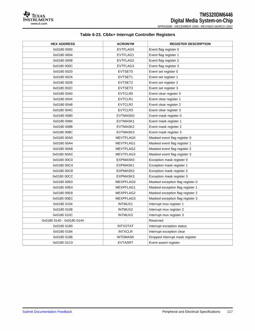
www.ti.com
TMS320DM6446Digital Media System-on-Chip
SPRS283E–DECEMBER 2005–REVISED MARCH 2007
Table 6-23. C64x+ Interrupt Controller Registers
HEX ADDRESS ACRONYM REGISTER DESCRIPTION
0x0180 0000 EVTFLAG0 Event flag register 0
0x0180 0004 EVTFLAG1 Event flag register 1
0x0180 0008 EVTFLAG2 Event flag register 2
0x0180 000C EVTFLAG3 Event flag register 3
0x0180 0020 EVTSET0 Event set register 0
0x0180 0024 EVTSET1 Event set register 1
0x0180 0028 EVTSET2 Event set register 2
0x0180 002C EVTSET3 Event set register 3
0x0180 0040 EVTCLR0 Event clear register 0
0x0180 0044 EVTCLR1 Event clear register 1
0x0180 0048 EVTCLR2 Event clear register 2
0x0180 004C EVTCLR3 Event clear register 3
0x0180 0080 EVTMASK0 Event mask register 0
0x0180 0084 EVTMASK1 Event mask register 1
0x0180 0088 EVTMASK2 Event mask register 2
0x0180 008C EVTMASK3 Event mask register 3
0x0180 00A0 MEVTFLAG0 Masked event flag register 0
0x0180 00A4 MEVTFLAG1 Masked event flag register 1
0x0180 00A8 MEVTFLAG2 Masked event flag register 2
0x0180 00AC MEVTFLAG3 Masked event flag register 3
0x0180 00C0 EXPMASK0 Exception mask register 0
0x0180 00C4 EXPMASK1 Exception mask register 1
0x0180 00C8 EXPMASK2 Exception mask register 2
0x0180 00CC EXPMASK3 Exception mask register 3
0x0180 00E0 MEXPFLAG0 Masked exception flag register 0
0x0180 00E4 MEXPFLAG1 Masked exception flag register 1
0x0180 00E8 MEXPFLAG2 Masked exception flag register 2
0x0180 00EC MEXPFLAG3 Masked exception flag register 3
0x0180 0104 INTMUX1 Interrupt mux register 1
0x0180 0108 INTMUX2 Interrupt mux register 2
0x0180 010C INTMUX3 Interrupt mux register 3
0x0180 0140 - 0x0180 0144 - Reserved
0x0180 0180 INTXSTAT Interrupt exception status
0x0180 0184 INTXCLR Interrupt exception clear
0x0180 0188 INTDMASK Dropped interrupt mask register
0x0180 01C0 EVTASRT Event assert register
Submit Documentation Feedback Peripheral and Electrical Specifications 117

www.ti.com
6.7.3 ARM/DSP Communications Interrupts
TMS320DM6446Digital Media System-on-ChipSPRS283E–DECEMBER 2005–REVISED MARCH 2007
The INTGEN register is used for generating interrupts between the ARM and DSP. The INTGEN registerformat is shown in Figure 6-18. Table 6-24 describes the register bit fields. The ARM may generate aninterrupt to the DSP by setting one of the four INTDSP[3:0] bits or the INTNMI bit. The interrupt bitautomatically self clears and the corresponding DSP[3:0]STAT or NMISTAT bit is automatically set toindicate that the interrupt was generated. After servicing the interrupt, the DSP clears the status bit bywriting ‘0’. The ARM may poll the status bit to determine when the DSP has completed servicing theinterrupt. The DSP may generate an interrupt to the ARM in the same manner using the INTARM[1:0] bitsand monitor ARM interrupt servicing via the ARM[1:0]STAT bits.
Figure 6-18. INTGEN Register
31 30 29 28 27 24 23 22 21 20 19 17 16
ARM1 ARM0 DSP3 DSP2 DSP1 DSP0 NMIReserved Reserved ReservedSTAT STAT STAT STAT STAT STAT STAT
R-00 R/W-0 R/W-0 R-0000 R/W-0 R/W-0 R/W-0 R/W-0 R-000 R/W-0
15 14 13 12 11 8 7 6 5 4 3 1 0
INT INT INT INT INT INT INTReserved Reserved ReservedARM1 ARM0 DSP3 DSP2 DSP1 DSP0 NMI
R-00 R/W-0 R/W-0 R-0000 R/W-0 R/W-0 R/W-0 R/W-0 R-000 R/W-0
LEGEND: R = Read, W = Write, n = value at reset
Table 6-24. INTGEN Register Bit Fields Descriptions
Name Description
ARM1STAT DSP to ARM Int1 Status/Clear (1)
ARM0STAT DSP to ARM Int0 Status/Clear (1)
DSP3STAT ARM to DSP Int3 Status/Clear (1)
DSP2STAT ARM to DSP Int2 Status/Clear (1)
DSP1STAT ARM to DSP Int1 Status/Clear (1)
DSP0STAT ARM to DSP Int0 Status/Clear (1)
NMISTAT DSP NMI Status/Clear (1)
INTARM1 DSP to ARM Int1 Set (2)
INTARM0 DSP to ARM Int0 Set (2)
INTDSP3 ARM to DSP Int3 Set (2)
INTDSP2 ARM to DSP Int2 Set (2)
INTDSP1 ARM to DSP Int1 Set (2)
INTDSP0 ARM to DSP Int0 Set (2)
INTNMI DSP NMI Set (2)
(1) Write '0' to clear. Writing '1' has no effect.(2) Write '1' to generate the interrupt. The register bit automatically clears to a value of '0'. Writing a '0' has no effect.
118 Peripheral and Electrical Specifications Submit Documentation Feedback

www.ti.com
6.8 General-Purpose Input/Output (GPIO)
TMS320DM6446Digital Media System-on-Chip
SPRS283E–DECEMBER 2005–REVISED MARCH 2007
The GPIO peripheral provides general-purpose pins that can be configured as either inputs or outputs.When configured as an output, a write to an internal register can control the state driven on the output pin.When configured as an input, the state of the input is detectable by reading the state of an internalregister. In addition, the GPIO peripheral can produce CPU interrupts and EDMA events in differentinterrupt/event generation modes. The GPIO peripheral provides generic connections to external devices.The GPIO pins are grouped into banks of 16 pins per bank (i.e., bank 0 consists of GPIO [0:15]).
The DM6446 GPIO peripheral supports the following:• Up to 54 1.8v GPIO pins, GPIO[0:53]• Up to 17 3.3v GPIO pins, GPIO3V[0:16] (GPIO[54:70])• Interrupts:
– Up to 8 unique GPIO[0:7] interrupts from Bank 0– 5 GPIO bank (aggregated) interrupt signals from each of the 5 banks of GPIOs– Interrupts can be triggered by rising and/or falling edge, specified for each interrupt capable GPIO
signal• DMA events:
– Up to 8 unique GPIO DMA events from Bank 0– 5 GPIO bank (aggregated) DMA event signals from each of the 5 banks of GPIOs
• Set/clear functionality: Firmware writes 1 to corresponding bit position(s) to set or to clear GPIOsignal(s). This allows multiple firmware processes to toggle GPIO output signals without critical sectionprotection (disable interrupts, program GPIO, re-enable interrupts, to prevent context switching toanther process during GPIO programming).
• Separate Input/Output registers• Output register in addition to set/clear so that, if preferred by firmware, some GPIO output signals can
be toggled by direct write to the output register(s).• Output register, when read, reflects output drive status. This, in addition to the input register reflecting
pin status and open-drain I/O cell, allows wired logic be implemented.
The memory map for the GPIO registers is shown in Table 6-25. For more detailed information on GPIOs,see the Documentation Support section for the General-Purpose Input/Output (GPIO) Reference Guide.
Submit Documentation Feedback Peripheral and Electrical Specifications 119

www.ti.com
6.8.1 GPIO Peripheral Register Description(s)
TMS320DM6446Digital Media System-on-ChipSPRS283E–DECEMBER 2005–REVISED MARCH 2007
Table 6-25. GPIO Registers
HEX ADDRESS RANGE ACRONYM REGISTER NAME
0x01C6 7000 PID Peripheral Identification Register
0x01C6 7004 - Reserved
0x01C6 7008 BINTEN GPIO interrupt per-bank enable
GPIO Banks 0 and 1
0x01C6 700C - Reserved
0x01C6 7010 DIR01 GPIO Banks 0 and 1 Direction Register (GPIO[0:31])
0x01C6 7014 OUT_DATA01 GPIO Banks 0 and 1 Output Data Register (GPIO[0:31])
0x01C6 7018 SET_DATA01 GPIO Banks 0 and 1 Set Data Register (GPIO[0:31])
0x01C6 701C CLR_DATA01 GPIO Banks 0 and 1 Clear data for banks 0 and 1 (GPIO[0:31])
0x01C6 7020 IN_DATA01 GPIO Banks 0 and 1 Input Data Register (GPIO[0:31])
0x01C6 7024 SET_RIS_TRIG01 GPIO Banks 0 and 1 Set Rising Edge Interrupt Register (GPIO[0:31])
0x01C6 7028 CLR_RIS_TRIG01 GPIO Banks 0 and 1 Clear Rising Edge Interrupt Register (GPIO[0:31])
0x01C6 702C SET_FAL_TRIG01 GPIO Banks 0 and 1 Set Falling Edge Interrupt Register (GPIO[0:31])
0x01C6 7030 CLR_FAL_TRIG01 GPIO Banks 0 and 1 Clear Falling Edge Interrupt Register (GPIO[0:31])
0x01C6 7034 INSTAT01 GPIO Banks 0 and 1 Interrupt Status Register (GPIO[0:31])
GPIO Banks 2 and 3
0x01C6 7038 DIR23 GPIO Banks 2 and 3 Direction Register (GPIO[32:63])
0x01C6 703C OUT_DATA23 GPIO Banks 2 and 3 Output Data Register (GPIO[32:63])
0x01C6 7040 SET_DATA23 GPIO Banks 2 and 3 Set Data Register (GPIO[32:63])
0x01C6 7044 CLR_DATA23 GPIO Banks 2 and 3 Clear Data Register (GPIO[32:63])
0x01C6 7048 IN_DATA23 GPIO Banks 2 and 3 Input Data Register (GPIO[32:63])
0x01C6 704C SET_RIS_TRIG23 GPIO Banks 2 and 3 Set Rising Edge Interrupt Register (GPIO[32:63])
0x01C6 7050 CLR_RIS_TRIG23 GPIO Banks 2 and 3 Clear Rising Edge Interrupt Register (GPIO[32:63])
0x01C6 7054 SET_FAL_TRIG23 GPIO Banks 2 and 3 Set Falling Edge Interrupt Register (GPIO[32:63])
0x01C6 7058 CLR_FAL_TRIG23 GPIO Banks 2 and 3 Clear Falling Edge Interrupt Register (GPIO[32:63])
0x01C6 705C INSTAT23 GPIO Banks 2 and 3 Interrupt Status Register (GPIO[32:63])
GPIO Bank 4
0x01C6 7060 DIR4 GPIO Bank 4 Direction Register (GPIO[64:70])
0x01C6 7064 OUT_DATA4 GPIO Bank 4 Output Data Register (GPIO[64:70])
0x01C6 7068 SET_DATA4 GPIO Bank 4 Set Data Register (GPIO[64:70])
0x01C6 706C CLR_DATA4 GPIO Bank 4 Clear Data Register (GPIO[64:70])
0x01C6 7070 IN_DATA4 GPIO Bank 4 Input Data Register (GPIO[64:70])
0x01C6 7074 SET_RIS_TRIG4 GPIO Bank 4 Set Rising Edge Interrupt Register (GPIO[64:70])
0x01C6 7078 CLR_RIS_TRIG4 GPIO Bank 4 Clear Rising Edge Interrupt Register (GPIO[64:70])
0x01C6 707C SET_FAL_TRIG4 GPIO Bank 4 Set Falling Edge Interrupt Register (GPIO[64:70])
0x01C6 7080 CLR_FAL_TRIG4 GPIO Bank 4 Clear Falling Edge Interrupt Register (GPIO[64:70])
0x01C6 7084 INSTAT4 GPIO Bank 4 Interrupt Status Register (GPIO[64:70])
0x01C6 7088 - 0x01C6 7FFF - Reserved
Peripheral and Electrical Specifications120 Submit Documentation Feedback

www.ti.com
6.8.2 GPIO Peripheral Input/Output Electrical Data/Timing
GPIx
GPOx
4
3
21
6.8.3 GPIO Peripheral External Interrupts Electrical Data/Timing
EXT_INTx
21
TMS320DM6446Digital Media System-on-Chip
SPRS283E–DECEMBER 2005–REVISED MARCH 2007
Table 6-26. Timing Requirements for GPIO Inputs (1) (see Figure 6-19)
-594NO. UNIT
MIN MAX
1 tw(GPIH) Pulse duration, GPIx high 52 ns
2 tw(GPIL) Pulse duration, GPIx low 52 ns
(1) The pulse width given is sufficient to generate a CPU interrupt or an EDMA event. However, if a user wants to have DM6446 recognizethe GPIx changes through software polling of the GPIO register, the GPIx duration must be extended to allow DM6446 enough time toaccess the GPIO register through the internal bus.
Table 6-27. Switching Characteristics Over Recommended Operating Conditions for GPIO Outputs(see Figure 6-19)
-594NO. PARAMETER UNIT
MIN MAX
3 tw(GPOH) Pulse duration, GPOx high 26 (1) ns
4 tw(GPOL) Pulse duration, GPOx low 26 (1) ns
(1) This parameter value should not be used as a maximum performance specification. Actual performance of back-to-back accesses of theGPIO is dependent upon internal bus activity.
Figure 6-19. GPIO Port Timing
Table 6-28. Timing Requirements for External Interrupts (1) (see Figure 6-20)
-594NO. UNIT
MIN MAX
1 tw(ILOW) Width of the external interrupt pulse low 52 ns
2 tw(IHIGH) Width of the external interrupt pulse high 52 ns
(1) The pulse width given is sufficient to generate an interrupt or an EDMA event. However, if a user wants to have DM6446recognize theGPIO changes through software polling of the GPIO register, the GPIO duration must be extended to allow DM6446 enough time toaccess the GPIO register through the internal bus.
Figure 6-20. GPIO External Interrupt Timing
Submit Documentation Feedback Peripheral and Electrical Specifications 121

www.ti.com
6.9 Enhanced Direct Memory Access (EDMA) Controller
6.9.1 EDMA Channel Synchronization Events
TMS320DM6446Digital Media System-on-ChipSPRS283E–DECEMBER 2005–REVISED MARCH 2007
The EDMA controller handles all data transfers between memories and the device slave peripherals onthe DM6446 device. These data transfers include cache servicing, non-cacheable memory accesses,user-programmed data transfers, and host accesses. These are summarized as follows:• Transfer to/from on-chip memories
– Coprocessor shared memory– DSP L1D memory– DSP L2 memory– ARM program/data RAM
• Transfer to/from external storage– DDR2 SDRAM– NAND flash– Asynchronous EMIF– Smart Media, SD, MMC, xD media storage– ATA/CF
• Transfer to/from peripherals/hosts– VLYNQ– ASP– SPI– PWM– UART
The EDMA controller supports two addressing modes: constant addressing mode and incrementaddressing mode. On the DM6446 device, constant addressing mode is not supported by any peripheralor internal memory. For more information on these two addressing modes, see the TMS320DM644xDMSoC Enhanced Direct Memory Access (EDMA) Controller User's Guide (literature number SPRUE23).
The EDMA supports up to 64 EDMA channels which service peripheral devices and external memory.Table 6-29 lists the source of EDMA synchronization events associated with each of the programmableEDMA channels. For the DM6446 device, the association of an event to a channel is fixed; each of theEDMA channels has one specific event associated with it. These specific events are captured in theEDMA event registers (ER, ERH) even if the events are disabled by the EDMA event enable registers(EER, EERH). For more detailed information on the EDMA module and how EDMA events are enabled,captured, processed, linked, chained, and cleared, etc., see the Document Support section of theTMS320DM644x DMSoC Enhanced Direct Memory Access (EDMA) Controller User's Guide (literaturenumber SPRUE23).
Table 6-29. DM6446 EDMA Channel Synchronization Events (1)
EDMA EVENT NAME EVENT DESCRIPTIONCHANNEL
0-1 Reserved
2 XEVT ASP Transmit Event
3 REVT ASP Receive Event
4 HISTEVT VPSS Histogram Event
5 H3AEVT VPSS H3A Event
6 PRVUEVT VPSS Previewer Event
(1) In addition to the events shown in this table, each of the 64 channels can also be synchronized with the transfer completion or alternatetransfer completion events. For more detailed information on EDMA event-transfer chaining, see the Document Support section of theTMS320DM644x DMSoC Enhanced Direct Memory Access (EDMA) Controller User's Guide (literature number SPRUE23).
Peripheral and Electrical Specifications122 Submit Documentation Feedback

www.ti.com
TMS320DM6446Digital Media System-on-Chip
SPRS283E–DECEMBER 2005–REVISED MARCH 2007
Table 6-29. DM6446 EDMA Channel Synchronization Events (continued)
EDMA EVENT NAME EVENT DESCRIPTIONCHANNEL
7 RSZEVT VPSS Resizer Event
8 IMXINT VICP Interrupt
9 VLCDINT VICP VLCD Interrupt
10 ASQINT VICP ASQ Interrupt
11 DSQINT VICP DSQ Interrupt
12-15 Reserved
16 SPIXEVT SPI Transmit Event
17 SPIREVT SPI Receive Event
18 URXEVT0 UART 0 Receive Event
19 UTXEVT0 UART 0 Transmit Event
20 URXEVT1 UART 1 Receive Event
21 UTXEVT1 UART 1 Transmit Event
22 URXEVT2 UART 2 Receive Event
23 UTXEVT2 UART 2 Transmit Event
24 Reserved
25 Reserved
26 MMCRXEVT MMC Receive Event
27 MMCTXEVT MMC Transmit Event
28 I2CREVT I2C Receive Event
29 I2CXEVT I2C Transmit Event
30-31 Reserved
32 GPINT0 GPIO 0 Interrupt
33 GPINT1 GPIO 1 Interrupt
34 GPINT2 GPIO 2 Interrupt
35 GPINT3 GPIO 3 Interrupt
36 GPINT4 GPIO 4 Interrupt
37 GPINT5 GPIO 5 Interrupt
38 GPINT6 GPIO 6 Interrupt
39 GPINT7 GPIO 7 Interrupt
40 GPBNKINT0 GPIO Bank 0 Interrupt
41 GPBNKINT1 GPIO Bank 1 Interrupt
42 GPBNKINT2 GPIO Bank 2 Interrupt
43 GPBNKINT3 GPIO Bank 3 Interrupt
44 GPBNKINT4 GPIO Bank 4 Interrupt
45-47 Reserved
48 TINT0 Timer 0 Interrupt
49 TINT1 Timer 1 Interrupt
50 TINT2 Timer 2 Interrupt
51 TINT3 Timer 3 Interrupt
52 PWM0 PWM 0 Event
53 PWM1 PWM 1 Event
54 PWM2 PWM 2 Event
55-63 Reserved
Submit Documentation Feedback Peripheral and Electrical Specifications 123

www.ti.com
TMS320DM6446Digital Media System-on-ChipSPRS283E–DECEMBER 2005–REVISED MARCH 2007
Peripheral and Electrical Specifications124 Submit Documentation Feedback

www.ti.com
6.9.2 EDMA Peripheral Register Descriptions
TMS320DM6446Digital Media System-on-Chip
SPRS283E–DECEMBER 2005–REVISED MARCH 2007
Table 6-30 lists the EDMA registers, their corresponding acronyms, and DM6446 device memorylocations.
Table 6-30. DM6446 EDMA Registers
HEX ADDRESS ACRONYM REGISTER NAME
Channel Controller Registers
0x01c0 0000 - 0x01c0 0003 Reserved
0x01c0 0004 CCCFG EDMA3CC Configuration Register
0x01c0 0008 - 0x01c0 01FF Reserved
Global Registers
0x01c0 0200 QCHMAP0 QDMA Channel 0 Mapping to PaRAM Register
0x01c0 0204 QCHMAP1 QDMA Channel 1 Mapping to PaRAM Register
0x01c0 0208 QCHMAP2 QDMA Channel 2 Mapping to PaRAM Register
0x01c0 020C QCHMAP3 QDMA Channel 3 Mapping to PaRAM Register
0x01c0 0210 QCHMAP4 QDMA Channel 4 Mapping to PaRAM Register
0x01c0 0214 QCHMAP5 QDMA Channel 5 Mapping to PaRAM Register
0x01c0 0218 QCHMAP6 QDMA Channel 6 Mapping to PaRAM Register
0x01c0 021C QCHMAP7 QDMA Channel 7 Mapping to PaRAM Register
0x01c0 0240 DMAQNUM0 DMA Queue Number Register 0 (Channels 00 to 07)
0x01c0 0244 DMAQNUM1 DMA Queue Number Register 1 (Channels 08 to 15)
0x01c0 0248 DMAQNUM2 DMA Queue Number Register 2 (Channels 16 to 23)
0x01c0 024C DMAQNUM3 DMA Queue Number Register 3 (Channels 24 to 31)
0x01c0 0250 DMAQNUM4 DMA Queue Number Register 4 (Channels 32 to 39)
0x01c0 0254 DMAQNUM5 DMA Queue Number Register 5 (Channels 40 to 47)
0x01c0 0258 DMAQNUM6 DMA Queue Number Register 6 (Channels 48 to 55)
0x01c0 025C DMAQNUM7 DMA Queue Number Register 7 (Channels 56 to 63)
0x01c0 0260 QDMAQNUM CC QDMA Queue Number
0x01c0 0264 - 0x01c0 0283 – Reserved
0x01c0 0284 QUEPRI Queue Priority Register
0x01c0 0288 - 0x01c0 02FF – Reserved
0x01c0 0300 EMR Event Missed Register
0x01c0 0304 EMRH Event Missed Register High
0x01c0 0308 EMCR Event Missed Clear Register
0x01c0 030C EMCRH Event Missed Clear Register High
0x01c0 0310 QEMR QDMA Event Missed Register
0x01c0 0314 QEMCR QDMA Event Missed Clear Register
0x01c0 0318 CCERR EDMA3CC Error Register
0x01c0 031C CCERRCLR EDMA3CC Error Clear Register
0x01c0 0320 EEVAL Error Evaluate Register
0x01c0 0340 DRAE0 DMA Region Access Enable Register for Region 0
0x01c0 0344 DRAEH0 DMA Region Access Enable Register High for Region 0
0x01c0 0348 DRAE1 DMA Region Access Enable Register for Region 1
0x01c0 034C DRAEH1 DMA Region Access Enable Register High for Region 1
0x01c0 0350 DRAE2 DMA Region Access Enable Register for Region 2
0x01c0 0354 DRAEH2 DMA Region Access Enable Register High for Region 2
0x01c0 0358 DRAE3 DMA Region Access Enable Register for Region 3
0x01c0 035C DRAEH3 DMA Region Access Enable Register High for Region 3
Submit Documentation Feedback Peripheral and Electrical Specifications 125

www.ti.com
TMS320DM6446Digital Media System-on-ChipSPRS283E–DECEMBER 2005–REVISED MARCH 2007
Table 6-30. DM6446 EDMA Registers (continued)
HEX ADDRESS ACRONYM REGISTER NAME
0x01c0 0360 - 0x01c0 037C – Reserved
0x01c0 0380 QRAE0 QDMA Region Access Enable Register for Region 0
0x01c0 0384 QRAE1 QDMA Region Access Enable Register for Region 1
0x01c0 0388 QRAE2 QDMA Region Access Enable Register for Region 2
0x01c0 038C QRAE3 QDMA Region Access Enable Register for Region 3
0x01c0 0390 - 0x01c0 039C – Reserved
0x01c0 0400 Q0E0 Event Q0 Entry 0 Register
0x01c0 0404 Q0E1 Event Q0 Entry 1 Register
0x01c0 0408 Q0E2 Event Q0 Entry 2 Register
0x01c0 040C Q0E3 Event Q0 Entry 3 Register
0x01c0 0410 Q0E4 Event Q0 Entry 4 Register
0x01c0 0414 Q0E5 Event Q0 Entry 5 Register
0x01c0 0418 Q0E6 Event Q0 Entry 6 Register
0x01c0 041C Q0E7 Event Q0 Entry 7 Register
0x01c0 0420 Q0E8 Event Q0 Entry 8 Register
0x01c0 0424 Q0E9 Event Q0 Entry 9 Register
0x01c0 0428 Q0E10 Event Q0 Entry 10 Register
0x01c0 042C Q0E11 Event Q0 Entry 11 Register
0x01c0 0430 Q0E12 Event Q0 Entry 12 Register
0x01c0 0434 Q0E13 Event Q0 Entry 13 Register
0x01c0 0438 Q0E14 Event Q0 Entry 14 Register
0x01c0 043C Q0E15 Event Q0 Entry 15 Register
0x01c0 0440 Q1E0 Event Q1 Entry 0 Register
0x01c0 0444 Q1E1 Event Q1 Entry 1 Register
0x01c0 0448 Q1E2 Event Q1 Entry 2 Register
0x01c0 044C Q1E3 Event Q1 Entry 3 Register
0x01c0 0450 Q1E4 Event Q1 Entry 4 Register
0x01c0 0454 Q1E5 Event Q1 Entry 5 Register
0x01c0 0458 Q1E6 Event Q1 Entry 6 Register
0x01c0 045C Q1E7 Event Q1 Entry 7 Register
0x01c0 0460 Q1E8 Event Q1 Entry 8 Register
0x01c0 0464 Q1E9 Event Q1 Entry 9 Register
0x01c0 0468 Q1E10 Event Q1 Entry 10 Register
0x01c0 046C Q1E11 Event Q1 Entry 11 Register
0x01c0 0470 Q1E12 Event Q1 Entry 12 Register
0x01c0 0474 Q1E13 Event Q1 Entry 13 Register
0x01c0 0478 Q1E14 Event Q1 Entry 14 Register
0x01c0 047C Q1E15 Event Q1 Entry 15 Register
0x01c0 0480 - 0x01c0 05FF Reserved
0x01c0 0600 QSTAT0 Queue 0 Status Register
0x01c0 0604 QSTAT1 Queue 1 Status Register
0x01c0 0608 - 0x01c0 061F Reserved
0x01c0 0620 QWMTHRA Queue Watermark Threshold A Register for Q[3:0]
0x01c0 0624 – Reserved
0x01c0 0640 CCSTAT EDMA3CC Status Register
0x01c0 0644 - 0x01c0 0FFF Reserved
Peripheral and Electrical Specifications126 Submit Documentation Feedback
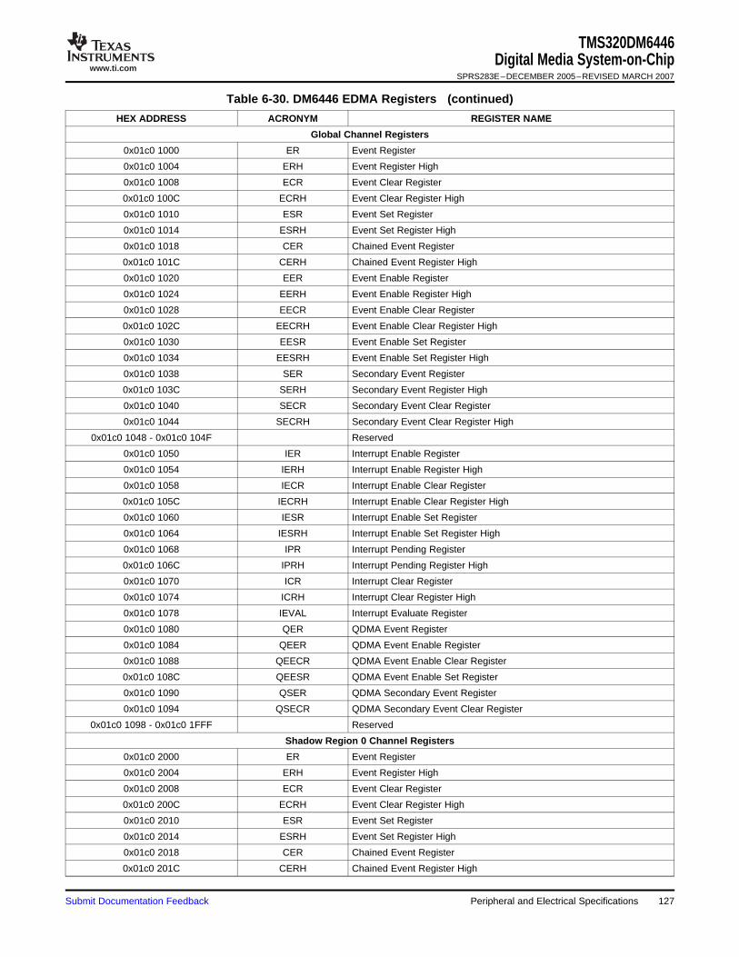
www.ti.com
TMS320DM6446Digital Media System-on-Chip
SPRS283E–DECEMBER 2005–REVISED MARCH 2007
Table 6-30. DM6446 EDMA Registers (continued)
HEX ADDRESS ACRONYM REGISTER NAME
Global Channel Registers
0x01c0 1000 ER Event Register
0x01c0 1004 ERH Event Register High
0x01c0 1008 ECR Event Clear Register
0x01c0 100C ECRH Event Clear Register High
0x01c0 1010 ESR Event Set Register
0x01c0 1014 ESRH Event Set Register High
0x01c0 1018 CER Chained Event Register
0x01c0 101C CERH Chained Event Register High
0x01c0 1020 EER Event Enable Register
0x01c0 1024 EERH Event Enable Register High
0x01c0 1028 EECR Event Enable Clear Register
0x01c0 102C EECRH Event Enable Clear Register High
0x01c0 1030 EESR Event Enable Set Register
0x01c0 1034 EESRH Event Enable Set Register High
0x01c0 1038 SER Secondary Event Register
0x01c0 103C SERH Secondary Event Register High
0x01c0 1040 SECR Secondary Event Clear Register
0x01c0 1044 SECRH Secondary Event Clear Register High
0x01c0 1048 - 0x01c0 104F Reserved
0x01c0 1050 IER Interrupt Enable Register
0x01c0 1054 IERH Interrupt Enable Register High
0x01c0 1058 IECR Interrupt Enable Clear Register
0x01c0 105C IECRH Interrupt Enable Clear Register High
0x01c0 1060 IESR Interrupt Enable Set Register
0x01c0 1064 IESRH Interrupt Enable Set Register High
0x01c0 1068 IPR Interrupt Pending Register
0x01c0 106C IPRH Interrupt Pending Register High
0x01c0 1070 ICR Interrupt Clear Register
0x01c0 1074 ICRH Interrupt Clear Register High
0x01c0 1078 IEVAL Interrupt Evaluate Register
0x01c0 1080 QER QDMA Event Register
0x01c0 1084 QEER QDMA Event Enable Register
0x01c0 1088 QEECR QDMA Event Enable Clear Register
0x01c0 108C QEESR QDMA Event Enable Set Register
0x01c0 1090 QSER QDMA Secondary Event Register
0x01c0 1094 QSECR QDMA Secondary Event Clear Register
0x01c0 1098 - 0x01c0 1FFF Reserved
Shadow Region 0 Channel Registers
0x01c0 2000 ER Event Register
0x01c0 2004 ERH Event Register High
0x01c0 2008 ECR Event Clear Register
0x01c0 200C ECRH Event Clear Register High
0x01c0 2010 ESR Event Set Register
0x01c0 2014 ESRH Event Set Register High
0x01c0 2018 CER Chained Event Register
0x01c0 201C CERH Chained Event Register High
Submit Documentation Feedback Peripheral and Electrical Specifications 127

www.ti.com
TMS320DM6446Digital Media System-on-ChipSPRS283E–DECEMBER 2005–REVISED MARCH 2007
Table 6-30. DM6446 EDMA Registers (continued)
HEX ADDRESS ACRONYM REGISTER NAME
0x01c0 2020 EER Event Enable Register
0x01c0 2024 EERH Event Enable Register High
0x01c0 2028 EECR Event Enable Clear Register
0x01c0 202C EECRH Event Enable Clear Register High
0x01c0 2030 EESR Event Enable Set Register
0x01c0 2034 EESRH Event Enable Set Register High
0x01c0 2038 SER Secondary Event Register
0x01c0 203C SERH Secondary Event Register High
0x01c0 2040 SECR Secondary Event Clear Register
0x01c0 2044 SECRH Secondary Event Clear Register High
0x01c0 2048 - 0x01c0 204C - Reserved
0x01c0 2050 IER Interrupt Enable Register
0x01c0 2054 IERH Interrupt Enable Register High
0x01c0 2058 IECR Interrupt Enable Clear Register
0x01c0 205C IECRH Interrupt Enable Clear Register High
0x01c0 2060 IESR Interrupt Enable Set Register
0x01c0 2064 IESRH Interrupt Enable Set Register High
0x01c0 2068 IPR Interrupt Pending Register
0x01c0 206C IPRH Interrupt Pending Register High
0x01c0 2070 ICR Interrupt Clear Register
0x01c0 2074 ICRH Interrupt Clear Register High
0x01c0 2078 IEVAL Interrupt Evaluate Register
0x01c0 207C - Reserved
0x01c0 2080 QER QDMA Event Register
0x01c0 2084 QEER QDMA Event Enable Register
0x01c0 2088 QEECR QDMA Event Enable Clear Register
0x01c0 208C QEESR QDMA Event Enable Set Register
0x01c0 2090 QSER QDMA Secondary Event Register
0x01c0 2094 QSECR QDMA Secondary Event Clear Register
0x01c0 2098 - 0x01c0 21FC - Reserved
Shadow Region 1 Channel Registers
0x01c0 2200 ER Event Register
0x01c0 2204 ERH Event Register High
0x01c0 2208 ECR Event Clear Register
0x01c0 220C ECRH Event Clear Register High
0x01c0 2210 ESR Event Set Register
0x01c0 2214 ESRH Event Set Register High
0x01c0 2218 CER Chained Event Register
0x01c0 221C CERH Chained Event Register High
0x01c0 2220 EER Event Enable Register
0x01c0 2224 EERH Event Enable Register High
0x01c0 2228 EECR Event Enable Clear Register
0x01c0 222C EECRH Event Enable Clear Register High
0x01c0 2230 EESR Event Enable Set Register
0x01c0 2234 EESRH Event Enable Set Register High
0x01c0 2238 SER Secondary Event Register
0x01c0 223C SERH Secondary Event Register High
Peripheral and Electrical Specifications128 Submit Documentation Feedback
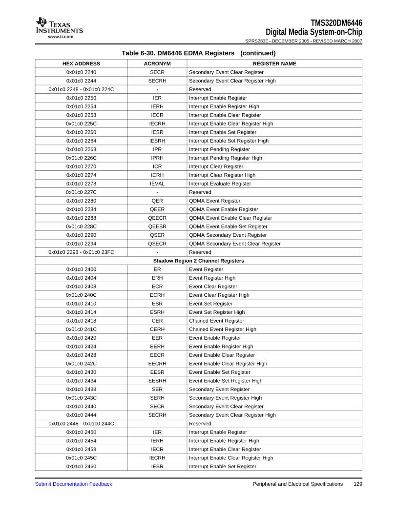
www.ti.com
TMS320DM6446Digital Media System-on-Chip
SPRS283E–DECEMBER 2005–REVISED MARCH 2007
Table 6-30. DM6446 EDMA Registers (continued)
HEX ADDRESS ACRONYM REGISTER NAME
0x01c0 2240 SECR Secondary Event Clear Register
0x01c0 2244 SECRH Secondary Event Clear Register High
0x01c0 2248 - 0x01c0 224C - Reserved
0x01c0 2250 IER Interrupt Enable Register
0x01c0 2254 IERH Interrupt Enable Register High
0x01c0 2258 IECR Interrupt Enable Clear Register
0x01c0 225C IECRH Interrupt Enable Clear Register High
0x01c0 2260 IESR Interrupt Enable Set Register
0x01c0 2264 IESRH Interrupt Enable Set Register High
0x01c0 2268 IPR Interrupt Pending Register
0x01c0 226C IPRH Interrupt Pending Register High
0x01c0 2270 ICR Interrupt Clear Register
0x01c0 2274 ICRH Interrupt Clear Register High
0x01c0 2278 IEVAL Interrupt Evaluate Register
0x01c0 227C - Reserved
0x01c0 2280 QER QDMA Event Register
0x01c0 2284 QEER QDMA Event Enable Register
0x01c0 2288 QEECR QDMA Event Enable Clear Register
0x01c0 228C QEESR QDMA Event Enable Set Register
0x01c0 2290 QSER QDMA Secondary Event Register
0x01c0 2294 QSECR QDMA Secondary Event Clear Register
0x01c0 2298 - 0x01c0 23FC - Reserved
Shadow Region 2 Channel Registers
0x01c0 2400 ER Event Register
0x01c0 2404 ERH Event Register High
0x01c0 2408 ECR Event Clear Register
0x01c0 240C ECRH Event Clear Register High
0x01c0 2410 ESR Event Set Register
0x01c0 2414 ESRH Event Set Register High
0x01c0 2418 CER Chained Event Register
0x01c0 241C CERH Chained Event Register High
0x01c0 2420 EER Event Enable Register
0x01c0 2424 EERH Event Enable Register High
0x01c0 2428 EECR Event Enable Clear Register
0x01c0 242C EECRH Event Enable Clear Register High
0x01c0 2430 EESR Event Enable Set Register
0x01c0 2434 EESRH Event Enable Set Register High
0x01c0 2438 SER Secondary Event Register
0x01c0 243C SERH Secondary Event Register High
0x01c0 2440 SECR Secondary Event Clear Register
0x01c0 2444 SECRH Secondary Event Clear Register High
0x01c0 2448 - 0x01c0 244C - Reserved
0x01c0 2450 IER Interrupt Enable Register
0x01c0 2454 IERH Interrupt Enable Register High
0x01c0 2458 IECR Interrupt Enable Clear Register
0x01c0 245C IECRH Interrupt Enable Clear Register High
0x01c0 2460 IESR Interrupt Enable Set Register
Submit Documentation Feedback Peripheral and Electrical Specifications 129

www.ti.com
TMS320DM6446Digital Media System-on-ChipSPRS283E–DECEMBER 2005–REVISED MARCH 2007
Table 6-30. DM6446 EDMA Registers (continued)
HEX ADDRESS ACRONYM REGISTER NAME
0x01c0 2464 IESRH Interrupt Enable Set Register High
0x01c0 2468 IPR Interrupt Pending Register
0x01c0 246C IPRH Interrupt Pending Register High
0x01c0 2470 ICR Interrupt Clear Register
0x01c0 2474 ICRH Interrupt Clear Register High
0x01c0 2478 IEVAL Interrupt Evaluate Register
0x01c0 247C - Reserved
0x01c0 2480 QER QDMA Event Register
0x01c0 2484 QEER QDMA Event Enable Register
0x01c0 2488 QEECR QDMA Event Enable Clear Register
0x01c0 248C QEESR QDMA Event Enable Set Register
0x01c0 2490 QSER QDMA Secondary Event Register
0x01c0 2494 QSECR QDMA Secondary Event Clear Register
0x01c0 2498 - 0x01c0 25FC - Reserved
Shadow Region 3 Channel Registers
0x01c0 2600 ER Event Register
0x01c0 2604 ERH Event Register High
0x01c0 2608 ECR Event Clear Register
0x01c0 260C ECRH Event Clear Register High
0x01c0 2610 ESR Event Set Register
0x01c0 2614 ESRH Event Set Register High
0x01c0 2618 CER Chained Event Register
0x01c0 261C CERH Chained Event Register High
0x01c0 2620 EER Event Enable Register
0x01c0 2624 EERH Event Enable Register High
0x01c0 2628 EECR Event Enable Clear Register
0x01c0 262C EECRH Event Enable Clear Register High
0x01c0 2630 EESR Event Enable Set Register
0x01c0 2634 EESRH Event Enable Set Register High
0x01c0 2638 SER Secondary Event Register
0x01c0 263C SERH Secondary Event Register High
0x01c0 2640 SECR Secondary Event Clear Register
0x01c0 2644 SECRH Secondary Event Clear Register High
0x01c0 2648 - 0x01c0 264C - Reserved
0x01c0 2650 IER Interrupt Enable Register
0x01c0 2654 IERH Interrupt Enable Register High
0x01c0 2658 IECR Interrupt Enable Clear Register
0x01c0 265C IECRH Interrupt Enable Clear Register High
0x01c0 2660 IESR Interrupt Enable Set Register
0x01c0 2664 IESRH Interrupt Enable Set Register High
0x01c0 2668 IPR Interrupt Pending Register
0x01c0 266C IPRH Interrupt Pending Register High
0x01c0 2670 ICR Interrupt Clear Register
0x01c0 2674 ICRH Interrupt Clear Register High
0x01c0 2678 IEVAL Interrupt Evaluate Register
0x01c0 267C - Reserved
0x01c0 2680 QER QDMA Event Register
Peripheral and Electrical Specifications130 Submit Documentation Feedback

www.ti.com
TMS320DM6446Digital Media System-on-Chip
SPRS283E–DECEMBER 2005–REVISED MARCH 2007
Table 6-30. DM6446 EDMA Registers (continued)
HEX ADDRESS ACRONYM REGISTER NAME
0x01c0 2684 QEER QDMA Event Enable Register
0x01c0 2688 QEECR QDMA Event Enable Clear Register
0x01c0 268C QEESR QDMA Event Enable Set Register
0x01c0 2690 QSER QDMA Secondary Event Register
0x01c0 2694 QSECR QDMA Secondary Event Clear Register
0x01c0 2698 - 0x01c0 27FC - Reserved
0x01c0 2800 - 0x01c0 29FC - Reserved
0x01c0 2A00 - 0x01c0 2BFC - Reserved
0x01c0 2C00 - 0x01c0 2DFC - Reserved
0x01c0 2E00 - 0x01c0 2FFC - Reserved
0x01c0 2FFD - 0x01c0 3FFF - Reserved
0x01c0 4000 - 0x01c0 4FFF - Parameter Set RAM (see Table 6-31)
0x01c0 5000 - 0x01c0 7FFF - Reserved
0x01c0 8000 - 0x01c0 FFFF - Reserved
Transfer Controller 0 Registers
0x01c1 0000 - Reserved
0x01c1 0004 TCCFG EDMA3 TC0 Configuration Register
0x01c1 0008 - 0x01c1 00FF - Reserved
0x01c1 0100 TCSTAT EDMA3 TC0 Channel Status Register
0x01c1 0104 - 0x01c1 0110 - Reserved
0x01c1 0114 - 0x01c1 011F - Reserved
0x01c1 0120 ERRSTAT EDMA3 TC0 Error Status Register
0x01c1 0124 ERREN EDMA3 TC0 Error Enable Register
0x01c1 0128 ERRCLR EDMA3 TC0 Error Clear Register
0x01c1 012C ERRDET EDMA3 TC0 Error Details Register
0x01c1 0130 ERRCMD EDMA3 TC0 Error Interrupt Command Register
0x01c1 0134 - 0x01c1 013F - Reserved
0x01c1 0140 RDRATE EDMA3 TC0 Read Rate Register
0x01c1 0144 - 0x01c1 01FF - Reserved
0x01c1 0200 - 0x01c1 023F - Reserved
0x01c1 0240 SAOPT EDMA3 TC0 Source Active Options Register
0x01c1 0244 SASRC EDMA3 TC0 Source Active Source Address Register
0x01c1 0248 SACNT EDMA3 TC0 Source Active Count Register
0x01c1 024C SADST EDMA3 TC0 Source Active Destination Address Register
0x01c1 0250 SABIDX EDMA3 TC0 Source Active Source B-Index Register
0x01c1 0254 SAMPPRXY EDMA3 TC0 Source Active Memory Protection Proxy Register
0x01c1 0258 SACNTRLD EDMA3 TC0 Source Active Count Reload Register
0x01c1 025C SASRCBREF EDMA3 TC0 Source Active Source Address B-Reference Register
0x01c1 0260 SADSTBREF EDMA3 TC0 Source Active Destination Address B-Reference Register
0x01c1 0264 - 0x01c1 027F - Reserved
0x01c1 0280 DFCNTRLD EDMA3 TC0 Destination FIFO Set Count Reload Register
0x01c1 0284 DFSRCBREF EDMA3 TC0 Destination FIFO Set Source Address B-Reference Register
EDMA3 TC0 Destination FIFO Set Destination Address B-Reference0x01c1 0288 DFDSTBREF Register
0x01c1 028C - 0x01c1 02FF - Reserved
0x01c1 0300 DFOPT0 EDMA3 TC0 Destination FIFO Options Register 0
0x01c1 0304 DFSRC0 EDMA3 TC0 Destination FIFO Source Address Register 0
Submit Documentation Feedback Peripheral and Electrical Specifications 131

www.ti.com
TMS320DM6446Digital Media System-on-ChipSPRS283E–DECEMBER 2005–REVISED MARCH 2007
Table 6-30. DM6446 EDMA Registers (continued)
HEX ADDRESS ACRONYM REGISTER NAME
0x01c1 0308 DFCNT0 EDMA3 TC0 Destination FIFO Count Register 0
0x01c1 030C DFDST0 EDMA3 TC0 Destination FIFO Destination Address Register 0
0x01c1 0310 DFBIDX0 EDMA3 TC0 Destination FIFO BIDX Register 0
0x01c1 0314 DFMPPRXY0 EDMA3 TC0 Destination FIFO Memory Protection Proxy Register 0
0x01c1 0318 - 0x01c1 033F - Reserved
0x01c1 0340 DFOPT1 EDMA3 TC0 Destination FIFO Options Register 1
0x01c1 0344 DFSRC1 EDMA3 TC0 Destination FIFO Source Address Register 1
0x01c1 0348 DFCNT1 EDMA3 TC0 Destination FIFO Count Register 1
0x01c1 034C DFDST1 EDMA3 TC0 Destination FIFO Destination Address Register 1
0x01c1 0350 DFBIDX1 EDMA3 TC0 Destination FIFO BIDX Register 1
0x01c1 0354 DFMPPRXY1 EDMA3 TC0 Destination FIFO Memory Protection Proxy Register 1
0x01c1 0358 - 0x01c1 037F - Reserved
0x01c1 0380 DFOPT2 EDMA3 TC0 Destination FIFO Options Register 2
0x01c1 0384 DFSRC2 EDMA3 TC0 Destination FIFO Source Address Register 2
0x01c1 0388 DFCNT2 EDMA3 TC0 Destination FIFO Count Register 2
0x01c1 038C DFDST2 EDMA3 TC0 Destination FIFO Destination Address Register 2
0x01c1 0390 DFBIDX2 EDMA3 TC0 Destination FIFO BIDX Register 2
0x01c1 0394 DFMPPRXY2 EDMA3 TC0 Destination FIFO Memory Protection Proxy Register 2
0x01c1 0398 - 0x01c1 03BF - Reserved
0x01c1 03C0 DFOPT3 EDMA3 TC0 Destination FIFO Options Register 3
0x01c1 03C4 DFSRC3 EDMA3 TC0 Destination FIFO Source Address Register 3
0x01c1 03C8 DFCNT3 EDMA3 TC0 Destination FIFO Count Register 3
0x01c1 03CC DFDST3 EDMA3 TC0 Destination FIFO Destination Address Register 3
0x01c1 03D0 DFBIDX3 EDMA3 TC0 Destination FIFO BIDX Register 3
0x01c1 03D4 DFMPPRXY3 EDMA3 TC0 Destination FIFO Memory Protection Proxy Register 3
0x01c1 03D8 - 0x01c1 03FF - Reserved
Transfer Controller 1 Registers
0x01c1 0400 - Reserved
0x01c1 0404 TCCFG EDMA3 TC1 Configuration Register
0x01c1 0408 - 0x01c1 04FF - Reserved
0x01c1 0500 TCSTAT EDMA3 TC1 Channel Status Register
0x01c1 0504 - 0x01c1 0510 - Reserved
0x01c1 0514 - 0x01c1 051F - Reserved
0x01c1 0520 ERRSTAT EDMA3 TC1 Error Status Register
0x01c1 0524 ERREN EDMA3 TC1 Error Enable Register
0x01c1 0528 ERRCLR EDMA3 TC1 Error Clear Register
0x01c1 052C ERRDET EDMA3 TC1 Error Details Register
0x01c1 0530 ERRCMD EDMA3 TC1 Error Interrupt Command Register
0x01c1 0534 - 0x01c1 053F - Reserved
0x01c1 0540 RDRATE EDMA3 TC1 Read Rate Register
0x01c1 0544 - 0x01c1 05FF - Reserved
0x01c1 0600 - 0x01c1 063F - Reserved
0x01c1 0640 SAOPT EDMA3 TC1 Source Active Options Register
0x01c1 0644 SASRC EDMA3 TC1 Source Active Source Address Register
0x01c1 0648 SACNT EDMA3 TC1 Source Active Count Register
0x01c1 064C SADST EDMA3 TC1 Source Active Destination Address Register
0x01c1 0650 SABIDX EDMA3 TC1 Source Active Source B-Index Register
Peripheral and Electrical Specifications132 Submit Documentation Feedback

www.ti.com
TMS320DM6446Digital Media System-on-Chip
SPRS283E–DECEMBER 2005–REVISED MARCH 2007
Table 6-30. DM6446 EDMA Registers (continued)
HEX ADDRESS ACRONYM REGISTER NAME
0x01c1 0654 SAMPPRXY EDMA3 TC1 Source Active Memory Protection Proxy Register
0x01c1 0658 SACNTRLD EDMA3 TC1 Source Active Count Reload Register
0x01c1 065C SASRCBREF EDMA3 TC1 Source Active Source Address B-Reference Register
0x01c1 0660 SADSTBREF EDMA3 TC1 Source Active Destination Address B-Reference Register
0x01c1 0664 - 0x01c1 067F - Reserved
0x01c1 0680 DFCNTRLD EDMA3 TC1 Destination FIFO Set Count Reload Register
0x01c1 0684 DFSRCBREF EDMA3 TC1 Destination FIFO Set Source Address B-Reference Register
EDMA3 TC1 Destination FIFO Set Destination Address B-Reference0x01c1 0688 DFDSTBREF Register
0x01c1 068C - 0x01c1 06FF - Reserved
0x01c1 0700 DFOPT0 EDMA3 TC1 Destination FIFO Options Register 0
0x01c1 0704 DFSRC0 EDMA3 TC1 Destination FIFO Source Address Register 0
0x01c1 0708 DFCNT0 EDMA3 TC1 Destination FIFO Count Register 0
0x01c1 070C DFDST0 EDMA3 TC1 Destination FIFO Destination Address Register 0
0x01c1 0710 DFBIDX0 EDMA3 TC1 Destination FIFO BIDX Register 0
0x01c1 0714 DFMPPRXY0 EDMA3 TC1 Destination FIFO Memory Protection Proxy Register 0
0x01c1 0718 - 0x01c1 073F - Reserved
0x01c1 0740 DFOPT1 EDMA3 TC1 Destination FIFO Options Register 1
0x01c1 0744 DFSRC1 EDMA3 TC1 Destination FIFO Source Address Register 1
0x01c1 0748 DFCNT1 EDMA3 TC1 Destination FIFO Count Register 1
0x01c1 074C DFDST1 EDMA3 TC1 Destination FIFO Destination Address Register 1
0x01c1 0750 DFBIDX1 EDMA3 TC1 Destination FIFO BIDX Register 1
0x01c1 0754 DFMPPRXY1 EDMA3 TC1 Destination FIFO Memory Protection Proxy Register 1
0x01c1 0758 - 0x01c1 077F - Reserved
0x01c1 0780 DFOPT2 EDMA3 TC1 Destination FIFO Options Register 2
0x01c1 0784 DFSRC2 EDMA3 TC1 Destination FIFO Source Address Register 2
0x01c1 0788 DFCNT2 EDMA3 TC1 Destination FIFO Count Register 2
0x01c1 078C DFDST2 EDMA3 TC1 Destination FIFO Destination Address Register 2
0x01c1 0790 DFBIDX2 EDMA3 TC1 Destination FIFO BIDX Register 2
0x01c1 0794 DFMPPRXY2 EDMA3 TC1 Destination FIFO Memory Protection Proxy Register 2
0x01c1 0798 - 0x01c1 07BF - Reserved
0x01c1 07C0 DFOPT3 EDMA3 TC1 Destination FIFO Options Register 3
0x01c1 07C4 DFSRC3 EDMA3 TC1 Destination FIFO Source Address Register 3
0x01c1 07C8 DFCNT3 EDMA3 TC1 Destination FIFO Count Register 3
0x01c1 07CC DFDST3 EDMA3 TC1 Destination FIFO Destination Address Register 3
0x01c1 07D0 DFBIDX3 EDMA3 TC1 Destination FIFO BIDX Register 3
0x01c1 07D4 DFMPPRXY3 EDMA3 TC1 Destination FIFO Memory Protection Proxy Register 3
0x01c1 07D8 - 0x01c1 07FF - Reserved
Table 6-31 shows an abbreviation of the set of registers which make up the parameter set for each of 128EDMA events. Each of the parameter register sets consist of 8 32-bit word entries. Table 6-32 shows theparameter set entry registers with relative memory address locations within each of the parameter sets.
Submit Documentation Feedback Peripheral and Electrical Specifications 133

www.ti.com
TMS320DM6446Digital Media System-on-ChipSPRS283E–DECEMBER 2005–REVISED MARCH 2007
Table 6-31. EDMA Parameter Set RAM
HEX ADDRESS RANGE DESCRIPTION
0x01c0 4000 - 0x01c0 401F Parameters Set 0 (8 32-bit words)
0x01c0 4020 - 0x01c0 403F Parameters Set 1 (8 32-bit words)
0x01c0 4040 - 0x01c0 405F Parameters Set 2 (8 32-bit words)
0x01c0 4060 - 0x01c0 407F Parameters Set 3 (8 32-bit words)
0x01c0 4080 - 0x01c0 409F Parameters Set 4 (8 32-bit words)
0x01c0 40A0 - 0x01c0 40BF Parameters Set 5 (8 32-bit words)
... ...
0x01c0 4FC0 - 0x01c0 4FDF Parameters Set 126 (8 32-bit words)
0x01c0 4FE0 - 0x01c0 4FFF Parameters Set 127 (8 32-bit words)
Table 6-32. Parameter Set Entries
HEX OFFSET ADDRESS ACRONYM PARAMETER ENTRYWITHIN THE PARAMETER SET
0x0000 OPT Option
0x0004 SRC Source Address
0x0008 A_B_CNT A Count, B Count
0x000C DST Destination Address
0x0010 SRC_DST_BIDX Source B Index, Destination B Index
0x0014 LINK_BCNTRLD Link Address, B Count Reload
0x0018 SRC_DST_CIDX Source C Index, Destination C Index
0x001C CCNT C Count
Peripheral and Electrical Specifications134 Submit Documentation Feedback

www.ti.com
6.10 External Memory Interface (EMIF)
6.10.1 Asynchronous EMIF (EMIFA)
TMS320DM6446Digital Media System-on-Chip
SPRS283E–DECEMBER 2005–REVISED MARCH 2007
DM6446 supports several memory and external device interfaces, including:• Asynchronous EMIF (EMIFA) for interfacing to NOR Flash, SRAM, etc.• NAND Flash• ATA/CF
The DM6446 Asynchronous EMIF (EMIFA) provides an 8-bit or 16-bit data bus, an address bus width upto 24-bits, and 4 dedicated chip selects, along with memory control signals. These signals are multiplexedbetween three peripherals:• EMIFA and NAND interfaces• ATA/CF• Host Port Interface
6.10.1.1 NAND (NAND, SmartMedia, xD)
The EMIFA interface provides both the asynchronous EMIF and NAND interfaces. Four chip selects areprovided and each are individually configurable to provide either EMIFA or NAND support. The NANDfeatures supported are as follows.• NAND flash on up to 4 asynchronous chip selects.• 8 and 16-bit data bus widths.• Programmable cycle timings.• Performs ECC calculation.• NAND Mode also supports SmartMedia/SSFDC (Solid State Floppy Disk Controller) and xD memory
cards• ARM ROM supports booting of the DM6446 ARM processor from NAND flash located at CS2
The memory map for EMIFA and NAND registers is shown in Table 6-33. For more details on the EMIFAand NAND interfaces, see the TMS320DM644x DMSoC Peripherals Overview Reference Guide (literaturenumber SPRUE19) and the TMS320DM644x DMSoC Asynchronous External Memory Interface (EMIF)User's Guide (literature number SPRUE20).
Submit Documentation Feedback Peripheral and Electrical Specifications 135

www.ti.com
TMS320DM6446Digital Media System-on-ChipSPRS283E–DECEMBER 2005–REVISED MARCH 2007
Table 6-33. EMIFA/NAND Registers
HEX ADDRESS RANGE ACRONYM REGISTER NAME
0x01E0 0000 - 0x01E0 0003 Reserved
0x01E0 0004 AWCCR Asynchronous Wait Cycle Configuration Register
0x01E0 0008 - 0x01E0 000F Reserved
0x01E0 0010 A1CR Asynchronous 1 Configuration Register (CS2 Space)
0x01E0 0014 A2CR Asynchronous 2 Configuration Register (CS3 Space)
0x01E0 0018 A3CR Asynchronous 3 Configuration Register (CS4 Space)
0x01E0 001C A4CR Asynchronous 4 Configuration Register (CS5 Space)
0x01E0 0020 - 0x01E0 003F - Reserved
0x01E0 0040 EIRR EMIF Interrupt Raw Register
0x01E0 0044 EIMR EMIF Interrupt Mask Register
0x01E0 0048 EIMSR EMIF Interrupt Mask Set Register
0x01E0 004C EIMCR EMIF Interrupt Mask Clear Register
0x01E0 0050 - 0x01E0 005F - Reserved
0x01E0 0060 NANDFCR NAND Flash Control Register
0x01E0 0064 NANDFSR NAND Flash Status Register
0x01E0 0070 NANDF1ECC NAND Flash 1 ECC Register (CS2 Space)
0x01E0 0074 NANDF2ECC NAND Flash 2 ECC Register (CS3 Space)
0x01E0 0078 NANDF3ECC NAND Flash 3 ECC Register (CS4 Space)
0x01E0 007C NANDF4ECC NAND Flash 4 ECC Register (CS5 Space)
0x01E0 0080 - 0x01E0 0FFF - Reserved
Peripheral and Electrical Specifications136 Submit Documentation Feedback

www.ti.com
TMS320DM6446Digital Media System-on-Chip
SPRS283E–DECEMBER 2005–REVISED MARCH 2007
6.10.1.2 EMIFA Electrical Data/Timing
Table 6-34. Timing Requirements for Asynchronous Memory Cycles for EMIFA Module (1)
(see Figure 6-21 and Figure 6-22)
-594NO. UNIT
MIN MAX
READS and WRITES
2 tw(EM_WAIT) Pulse duration, EM_WAIT assertion and deassertion 2E ns
READS
12 tsu(EMDV-EMOEH) Setup time, EM_D[15:0] valid before EM_OE high 10.5 ns
13 th(EMOEH-EMDIV) Hold time, EM_D[15:0] valid after EM_OE high 0 ns
14 tsu(EMWAIT-EMOEH) Setup time, EM_WAIT asserted before EM_OE high (2) 4E + 10.4 ns
WRITES
28 tsu(EMWAIT-EMWEH) Setup time, EM_WAIT asserted before EM_WE high (2) 4E + 10.4 ns
(1) E = SYSCLK5 period in ns for EMIFA. For example, when running the DSP CPU at 594 MHz, use E = 10.1 ns.(2) Setup before end of STROBE phase (if no extended wait states are inserted) by which EM_WAIT must be asserted to add extended
wait states. Figure 6-23 and Figure 6-24 describe EMIF transactions that include extended wait states inserted during the STROBEphase. However, cycles inserted as part of this extended wait period should not be counted; the 4E requirement is to the start of wherethe HOLD phase would begin if there were no extended wait cycles.
Submit Documentation Feedback Peripheral and Electrical Specifications 137

www.ti.com
TMS320DM6446Digital Media System-on-ChipSPRS283E–DECEMBER 2005–REVISED MARCH 2007
Table 6-35. Switching Characteristics Over Recommended Operating Conditions for AsynchronousMemory Cycles for EMIFA Module (1) (2) (see Figure 6-21 and Figure 6-22)
-594NO. PARAMETER UNIT
MIN MAX
READS and WRITES
1 td(TURNAROUND) Turn around time (TA + 1) * E - 2 (TA + 1) * E + 2 ns
READS
(RS + RST + RH + (RS + RST + RH + TA +EMIF read cycle time (EW = 0) nsTA + 4) * E - 0.5 4) * E + 0.53 tc(EMRCYCLE)
(RS + RST + RH +EMIF read cycle time (EW = 1) 4184 * E + 0.5 nsTA + 4) * E - 0.5
Output setup time, EM_CS[5:2] low to EM_OE low (SS (RS + 1) * E - 1 (RS + 1) * E + 1.2 ns= 0)4 tsu(EMCSL-EMOEL)
Output setup time, EM_CS[5:2] low to EM_OE low (SS -1 ns= 1)
Output hold time, EM_OE high to EM_CS[5:2] high (RH + 1) * E - 1.3 (RH + 1) * E + 1.4 ns(SS = 0)5 th(EMOEH-EMCSH)
Output hold time, EM_OE high to EM_CS[5:2] high -1.4 ns(SS = 1)
6 tsu(EMBAV-EMOEL) Output setup time, EM_BA[1:0] valid to EM_OE low (RS + 1) * E - 1.8 (RS + 1) * E + 1.3 ns
7 th(EMOEH-EMBAIV) Output hold time, EM_OE high to EM_BA[1:0] invalid (RH + 1) * E - 2.1 (RH + 1) * E + 1.1 ns
8 tsu(EMAV-EMOEL) Output setup time, EM_A[21:0] valid to EM_OE low (RS + 1) * E - 1.9 (RS + 1) * E + 1.5 ns
9 th(EMOEH-EMAIV) Output hold time, EM_OE high to EM_A[21:0] invalid (RH + 1) * E - 2.4 (RH + 1) * E + 1.2 ns
EM_OE active low width (EW = 0) (RST + 1) * E - 2 (RST + 1) * E + 2 ns10 tw(EMOEL)
EM_OE active low width (EW = 1) (RST + 1) * E - 2 (RST + 4097) * E + 2 ns
11 td(EMWAITH-EMOEH) Delay time from EM_WAIT deasserted to EM_OE high 4E + 10.4 ns
WRITES
(WS + WST + WH (WS + WST + WH + TAEMIF write cycle time (EW = 0) ns+ TA + 4) * E - 0.5 + 4) * E + 0.515 tc(EMWCYCLE)
(WS + WST + WHEMIF write cycle time (EW = 1) 4184 * E + 0.5 ns+ TA + 4) * E -0.5
Output setup time, EM_CS[5:2] low to EM_WE low (WS + 1) * E - 0.9 (WS + 1) * E + 1.4 ns(SS = 0)16 tsu(EMCSL-EMWEL)
Output setup time, EM_CS[5:2] low to EM_WE low -1 ns(SS = 1)
Output hold time, EM_WE high to EM_CS[5:2] high (WH + 1) * E - 1.4 (WH + 1) * E + 1.1 ns(SS = 0)17 th(EMWEH-EMCSH)
Output hold time, EM_WE high to EM_CS[5:2] high -1.4 ns(SS = 1)
18 tsu(EMRNW-EMWEL) Output setup time, EM_R/W valid to EM_WE low (WS + 1) * E - 0.7 (WS + 1) * E + 0.9 ns
19 th(EMWEH-EMRNW) Output hold time, EM_WE high to EM_R/W invalid (WH + 1) * E - 0.9 (WH + 1) * E + 0.9 ns
20 tsu(EMBAV-EMWEL) Output setup time, EM_BA[1:0] valid to EM_WE low (WS + 1) * E - 1.7 (WS + 1) * E + 1.5 ns
21 th(EMWEH-EMBAIV) Output hold time, EM_WE high to EM_BA[1:0] invalid (WH + 1) * E - 2.2 (WH + 1) * E + 0.9 ns
22 tsu(EMAV-EMWEL) Output setup time, EM_A[21:0] valid to EM_WE low (WS + 1) * E - 1.8 (WS + 1) * E + 1.7 ns
23 th(EMWEH-EMAIV) Output hold time, EM_WE high to EM_A[21:0] invalid (WH + 1) * E - 2.5 (WH + 1) * E + 1 ns
EM_WE active low width (EW = 0) (WST + 1) * E - 2 (WST + 1) * E + 2 ns24 tw(EMWEL)
EM_WE active low width (EW = 1) (WST + 1) * E - 2 (WST + 4097) * E + 2
25 td(EMWAITH-EMWEH) Delay time from EM_WAIT deasserted to EM_WE high 4E + 10.4 ns
(1) RS = Read setup, RST = Read STrobe, RH = Read Hold, WS = Write Setup, WST = Write STrobe, WH = Write Hold, TA = TurnAround, EW = Extend Wait mode, SS = Select Strobe mode. These parameters are programmed via the Asynchronous Bank andAsynchronous Wait Cycle Configuration Registers and support the following range of values: TA[3:0], RS[15:0], RST[63:0], RH[7:0],WS[15:0], WST[63:0], WH[7:0], and EW[255:0]. For more information, see the TMS320DM644x DMSoC Asynchronous External MemoryInterface (EMIF) User's Guide (literature number SPRUE20).
(2) E = SYSCLK5 period in ns for EMIFA. For example, when running the DSP CPU at 594 MHz, use E = 10.1 ns.
Peripheral and Electrical Specifications138 Submit Documentation Feedback

www.ti.com
SETUP STROBE HOLD
EM_CS[5:2]
EM_BA[1:0]
13
12
EM_A[21:0]
EM_OE
EM_D[15:0]
EM_WE
10
59
7
48
6
3
1
EM_R/W
TMS320DM6446Digital Media System-on-Chip
SPRS283E–DECEMBER 2005–REVISED MARCH 2007
Table 6-35. Switching Characteristics Over Recommended Operating Conditions for AsynchronousMemory Cycles for EMIFA Module (see Figure 6-21 and Figure 6-22) (continued)
-594NO. PARAMETER UNIT
MIN MAX
26 tsu(EMDV-EMWEL) Output setup time, EM_D[15:0] valid to EM_WE low (WS + 1) * E - 2.2 (WS + 1) * E + 1.4 ns
27 th(EMWEH-EMDIV) Output hold time, EM_WE high to EM_D[15:0] invalid (WH + 1) * E - 2.2 (WH + 1) * E + 1.4 ns
Figure 6-21. Asynchronous Memory Read Timing for EMIF
Submit Documentation Feedback Peripheral and Electrical Specifications 139

www.ti.com
SETUP STROBE HOLD
EM_CS[5:2]
EM_BA[1:0]
EM_A[21:0]
EM_WE
EM_D[15:0]
EM_OE
EM_R/W
15
1
16
18
20
2224
17
19
21
23
26
27
EM_CS[5:2]
11
Asserted Deasserted
22
EM_BA[1:0]
EM_A[21:0]
EM_D[15:0]
EM_OE
EM_WAIT
SETUP STROBE Extended Due to EM_WAIT STROBE HOLD
14
TMS320DM6446Digital Media System-on-ChipSPRS283E–DECEMBER 2005–REVISED MARCH 2007
Figure 6-22. Asynchronous Memory Write Timing for EMIF
Figure 6-23. EM_WAIT Read Timing Requirements
Peripheral and Electrical Specifications140 Submit Documentation Feedback

www.ti.com
EM_CS[5:2]
25
Asserted Deasserted
22
EM_BA[1:0]
EM_A[21:0]
EM_D[15:0]
EM_WE
EM_WAIT
SETUP STROBE Extended Due to EM_WAIT STROBE HOLD
28
6.10.2 DDR2 Memory Controller
TMS320DM6446Digital Media System-on-Chip
SPRS283E–DECEMBER 2005–REVISED MARCH 2007
Figure 6-24. EM_WAIT Write Timing Requirements
The DDR2 Memory Controller is a dedicated interface to DDR2 SDRAM. It supports JESD79D-2Astandard compliant DDR2 SDRAM Devices and can interface to either 16-bit or 32-bit DDR2 SDRAMdevices. For details on the DDR2 Memory Controller, see Section 2.8.3, Document Support for the link tothe TMS320DM644x DMSoC Peripherals Overview Reference Guide (literature number SPRUE19) for theTMS320DM644x DMSoC DDR2 Memory Controller User's Guide (literature number SPRUE22).
DDR2 SDRAM plays a key role in a DaVinci-based system. Such a system is expected to require asignificant amount of high-speed external memory for:• Buffering of input image data from sensors or video sources• Intermediate buffering for processing/resizing of image data in the VPFE• Numerous OSD display buffers• Intermediate buffering for large raw Bayer data image files while performing image processing
functions• Buffering for intermediate data while performing video encode and decode functions• Storage of executable code for both the ARM and DSP
A memory map of the DDR2 Memory Controller registers is shown in Table 6-36.
Table 6-36. DDR2 Memory Controller Registers
HEX ADDRESS RANGE ACRONYM REGISTER NAME
0x01C4 004C DDRVTPER DDR2 VTP Enable Register
0x01C4 2030 DDRVTPR DDR2 VTP Register
0x2000 0000 - 0x2000 0003 - Reserved
0x2000 0004 SDRSTAT SDRAM Status Register
0x2000 0008 SDBCR SDRAM Bank Configuration Register
0x2000 000C SDRCR SDRAM Refresh Control Register
0x2000 0010 SDTIMR SDRAM Timing Register
0x2000 0014 SDTIMR2 SDRAM Timing Register 2
0x2000 0020 PBBPR Peripheral Bus Burst Priority Register
0x2000 0024 - 0x2000 00BF - Reserved
0x2000 00C0 IRR Interrupt Raw Register
0x2000 00C4 IMR Interrupt Masked Register
Submit Documentation Feedback Peripheral and Electrical Specifications 141

www.ti.com
DDR_CLK0
1
TMS320DM6446Digital Media System-on-ChipSPRS283E–DECEMBER 2005–REVISED MARCH 2007
Table 6-36. DDR2 Memory Controller Registers (continued)
HEX ADDRESS RANGE ACRONYM REGISTER NAME
0x2000 00C8 IMSR Interrupt Mask Set Register
0x2000 00CC IMCR Interrupt Mask Clear Register
0x2000 00D0 - 0x2000 00E3 - Reserved
0x2000 00E4 DDRPHYCR DDR PHY Control Register
0x2000 00E8 - 0x2000 00EF - Reserved
0x2000 00F0 VTPIOCR VTP IO Control Register
0x2000 00F4 - 0x2000 7FFF - Reserved
6.10.2.1 DDR2 Memory Controller Electrical Data/Timing
The Implementing DDR2 PCB Layout on the DM644x DMSoC application report (literature numberSPRAAC5) specifies a complete DDR2 interface solution for the DM6446 as well as a list of compatibleDDR2 devices. TI has performed the simulation and system characterization to ensure all DDR2 interfacetimings in this solution are met.
TI only supports board designs that follow the guidelines outlined in the Implementing DDR2 PCB Layouton the DM644x DMSoC application report (literature number SPRAAC5).
Table 6-37. Switching Characteristics Over Recommended Operating Conditions for DDR2 MemoryController (1) (2)(see Figure 6-25)
-594NO. PARAMETER UNIT
MIN MAX
1 tc(DDR_CLK0) Cycle time, DDR_CLK0 6 8 ns
(1) DDR_CLK0 cycle time = 2 x PLL2 - SYSCLK2 cycle time.(2) The PLL2 Controller must be programmed such that the resulting DDR_CLK0 clock frequency is within the specified range.
Figure 6-25. DDR2 Memory Controller Clock Timing
142 Peripheral and Electrical Specifications Submit Documentation Feedback

www.ti.com
6.11 ATA/CF
6.11.1 ATA/CF Peripheral Register Description(s)
TMS320DM6446Digital Media System-on-Chip
SPRS283E–DECEMBER 2005–REVISED MARCH 2007
The ATA/CF peripheral supports the following features:• PIO, multiword DMA, and Ultra ATA 33/66• Up to mode 4 timings on PIO mode• Up to mode 2 timings on multiword DMA• Up to mode 4 timings on Ultra ATA• Programmable timing parameters• Supports TrueIDE mode for Compact Flash
In addition, the Host IDE Controller supports multiword DMA transfers between external IDE/ATAPIdevices and a system memory bus interface.
The ATA registers are shown in Table 6-38.
Table 6-38. ATA Register Memory Map
HEX ADDRESS RANGE ACRONYM REGISTER NAME
ATA Bus Master Interface DMA Engine Registers
0x01C6 6000 BMICP Primary IDE Channel DMA Control Register
0x01C6 6002 BMISP Primary IDE Channel DMA Status Register
0x01C6 6004 BMIDTP Primary IDE Channel DMA Descriptor Table Pointer Register
0x01C6 6008 -
0x01C6 600A - Reserved
0x01C6 600C -
ATA Configuration Registers
0x01C6 6040 IDETIMP Primary IDE Channel Timing Register
0x01C6 6042 -
0x01C6 6044 - Reserved
0x01C6 6045 -
0x01C6 6047 IDESTAT IDE Controller Status Register
0x01C6 6048 UDMACTL Ultra-DMA Control Register
0x01C6 604A - Reserved
0x01C6 6050 MISCCTL Miscellaneous Control Register
0x01C6 6054 REGSTB Task File Register Strobe Timing Register
0x01C6 6058 REGRCVR Task File Register Recovery Timing Register
0x01C6 605C DATSTB Data Register Access PIO Strobe Timing Register
0x01C6 6060 DATRCVR Data Register Access PIO Recovery Timing Register
0x01C6 6064 DMASTB Multiword DMA Strobe Timing Register
0x01C6 6068 DMARCVR Multiword DMA Recovery Timing Register
0x01C6 606C UDMASTB Ultra-DMA Strobe Timing Register
0x01C6 6070 UDMATRP Ultra-DMA Ready-to-Pause Timing Register
0x01C6 6074 UDMATENV Ultra-DMA Timing Envelope Register
0x01C6 6078 IORDYTMP Primary IO Ready Timer Configuration Register
0x01C6 607C - 0x01C6 67FF - Reserved
Submit Documentation Feedback Peripheral and Electrical Specifications 143

www.ti.com
6.11.2 ATA/CF Electrical Data/Timing
TMS320DM6446Digital Media System-on-ChipSPRS283E–DECEMBER 2005–REVISED MARCH 2007
All ATA/CF AC timing data described in Section 6.11.2.1–Section 6.11.2.3 is provided at the DM6446device pins. For more details, see Section 6.1, Parameter Information.
The AC timing specifications described in Section 6.11.2.1–Section 6.11.2.3 assume correct configurationof the ATA/CF memory-mapped control registers for the selected ATA/CF frequency of operation.
6.11.2.1 ATA/CF PIO Data Transfer AC Timing
Table 6-39. Timings for ATA/CF Module — PIO Data Transfer (1) (2) (see Figure 6-26)
-594NO. UNIT
MODE MIN MAX
1 t0 Cycle time 0-4 (3) (DATSTB + DATRCVR + 2)P -0.5 ns
2 t1 Address valid to DIOW/ DIOR setup 0-4 (3) 12P - 1.6 ns
3 t2 DIOW/ DIOR pulse duration low 0-4 (3) (DATSTB + 1)P - 1ns
0-2 – ns4 t2i DIOW/DIOR recovery time, pulse duration high
3-4 (3) (DATRCVR + 1)P - 1 ns
DIOW data setup time, DD[15:0] valid before5 t3 0-4 (3) (DATSTB + 1)P nsDIOW rising edge
DIOW data hold time, DD[15:0] valid after DIOW6 t4 0-4 (3) (HWNHLD + 1)P + 1 nsrising edge
0 50 nsDIOR data setup time, DD[15:0] valid before DIOR7 t5 1 35 nsrising edge
2-4 (3) 20 ns
DIOR data hold time, DD[15:0] valid after DIOR8 t6 0-4 (3) 5 nsrising edge
Output data 3-state, DD[15:0] 3-state after DIOR9 t6Z 0-4 (3) 30 nsrising edge
10 t9 DIOW/DIOR to address valid hold 0-4 (3) (HWNHLD + 1)P - 2.1 ns
Read data setup time, DD[15:0] valid before11 tRD 0-4 (3) 0 nsIORDY active
12 tA IORDY setup 0-4 (3) (4) 35 ns
13 tB IORDY pulse width 0-4 (3) 1250 ns
14 tC IORDY assertion to release 0-4 (3) 5 ns
(1) P = SYSCLK5 period, in ns, for ATA. For example, when running the DSP CPU at 594 MHz, use P = 10.1 ns.(2) DATSTB equals the value programmed in the DATSTBxP bit field in the DATSTB register. DATRCVR equals the value programmed in
the DATRCVRxP bit field in the DATRCVR register. HWNHLD equals the value programmed in the HWNHLDxP bit field in theMISCCTL register. For more detailed information, see the TMS320DM644x DMSoC ATA Controller User's Guide (literature numberSPRUE21).
(3) The sustained throughput for PIO modes 3 and 4 is limited to the throughput equivalent of PIO mode 2. For more detailed information,see the TMS320DM644x DMSoC ATA Controller User's Guide (literature number SPRUE21).
(4) The tA parameter must be met only when the IORDY timer is enabled to allow a device to insert wait states during a transaction. In orderto meet the tA parameter, a minimum frequency for SYSCLK5 is specified for each PIO as follows:• PIO mode 0, MIN frequency = 15 MHz• PIO mode 1, MIN frequency = 22 MHz• PIO mode 2, MIN frequency = 31 MHz• PIO mode 3, MIN frequency = 45 MHz• PIO mode 4, MIN frequency = 57 MHz
Peripheral and Electrical Specifications144 Submit Documentation Feedback

www.ti.com
DA[2:0],ATA_CS0,ATA_CS1
t4
t0
IORDY(A)
DIOW/DIOR
DD[15:0](OUT)
DD[15:0] (IN)
IORDY(B)
IORDY(C)
t1 t2 t9
t2it3
t6t5
t6Z
tRDtC
tA
tC
tB
A. IORDY is not negated for transfer (no wait generated)B. IORDY is negative but is re-assert before tA (no wait is generated)C. IORDY is negative before tA and remains asserted until tB; data is driven valid at tRD (wait is generated)
TMS320DM6446Digital Media System-on-Chip
SPRS283E–DECEMBER 2005–REVISED MARCH 2007
Figure 6-26. ATA/CF PIO Data Transfer Timing
Submit Documentation Feedback Peripheral and Electrical Specifications 145

www.ti.com
TMS320DM6446Digital Media System-on-ChipSPRS283E–DECEMBER 2005–REVISED MARCH 2007
6.11.2.2 ATA/CF Multiword DMA Timing
Table 6-40. Timings for ATA/CF Module — Multiword DMA AC Timing (1) (2) (see Figure 6-27)
-594NO. UNIT
MODE MIN MAX
1 t0 Cycle time 0-2 (DMASTB + DMARCVR + 2)P - 0.5 ns
2 tD DIOW/DIOR active low pulse duration 0-2 (DMASTB + 1)P - 1 ns
0 150 nsDIOR data access, DIOR falling edge to DD[15:0]3 tE 1 60 nsvalid
2 50 ns
DIOR data hold time, DD[15:0] valid after DIOR4 tF 0-2 5 nsrising edge
DIOW/DIOR data setup time, DD[15:0] (OUT) valid 0-2 (DMASTB)P nsbefore DIOW/DIOR rising edge
0 100 ns5 tGDIOW/DIOR data setup time, DD[15:0] (IN) valid 1 30 nsbefore DIOW/DIOR rising edge
2 20 ns
DIOW data hold time, DD[15:0] valid after DIOW6 tH 0-2 (HWNHLD + 1)P + 1 nsrising edge
7 tI DMACK to DIOW/DIOR setup 0-2 (DMARCVR + 1)P - 1.7 ns
8 tJ DIOW/DIOR to DMACK hold 0-2 5P - 5.9 ns
9 tKR DIOR negated pulse width 0-2 (DMARCVR + 1)P - 1 ns
10 tKW DIOW negated pulse width 0-2 (DMARCVR + 1)P - 1 ns
0 120 ns
11 tLR DIOR to DMARQ delay 1 45 ns
2 35 ns
0-1 40 ns12 tLW DIOW to DMARQ delay
2 35 ns
13 tM ATA_CSx valid to DIOW/DIOR setup 0-2 (DATRCVR)P - 1.7 ns
14 tN ATA_CSx valid after DIOW/DIOR rising edge hold 0-2 5P - 1.7 ns
0 20 ns15 tZ DMACK to read data (DD[15:0]) released
1-2 25 ns
(1) P = SYSCLK5 period, in ns, for ATA. For example, when running the DSP CPU at 594 MHz, use P = 10.1 ns.(2) DMASTB equals the value programmed in the DMASTBxP bit field in the DMASTB register. DMARCVR equals the value programmed
in the DMARCVRxP bit field in the DMARCVR register. HWNHLD equals the value programmed in the HWNHLDxP bit field in theMISCCTL register. For more detailed information, see the TMS320DM644x DMSoC ATA Controller User's Guide (literature numberSPRUE21).
Peripheral and Electrical Specifications146 Submit Documentation Feedback

www.ti.com
DA[2:0],ATA_CS0,ATA_CS1
tM t0tN
tL
tJ
tZ
tK
tH
tF
tDtI
tG
tE
tG
DMARQ
DMACK
DIOW/DIOR
DD[15:0](OUT)
DD[15:0] (IN)
TMS320DM6446Digital Media System-on-Chip
SPRS283E–DECEMBER 2005–REVISED MARCH 2007
Figure 6-27. ATA/CF Multiword DMA Timing
Submit Documentation Feedback Peripheral and Electrical Specifications 147

www.ti.com
TMS320DM6446Digital Media System-on-ChipSPRS283E–DECEMBER 2005–REVISED MARCH 2007
6.11.2.3 ATA/CF Ultra DMA Timing
Table 6-41. Timings for ATA/CF Module — Ultra DMA AC Timing (1) (2)
(see Figure 6-28 through Figure 6-37)
-594NO. UNIT
MODE MIN MAX
28 f(SYSCLK5) Operating frequency, SYSCLK5 0-4 25 MHz
0 240 ns
1 160 ns
1 t2CYCTYP Typical sustained average two cycle time 2 120 ns
3 90 ns
4 60 ns
2 tCYC Cycle time, Strobe edge to Strobe edge 0-4 (UDMASTB + 1)P ns
Two cycle time, rising to rising edge or falling to3 t2CYC 0-4 2(UDMASTB + 1)P nsfalling edge
0 15 ns
1 10 ns4 tDS Data setup, data valid before STROBE edge
2-3 7 ns
4 5 ns
5 tDH Data hold, data valid after STROBE edge 0-4 5 ns
0 70 ns
1 48 nsData valid INPUT setup time, data valid before 2 31 nsSTROBE
6 tDVS 3 20 ns
4 6.7 ns
Data valid OUTPUT setup time, data valid before 0-4 (UDMASTB)P - 3.1 nsSTROBE
Data valid INPUT hold time, data valid after 0-4 6.2 nsSTROBE7 tDVH
Data valid OUTPUT hold time, data valid after 0-4 1P - 2 nsSTROBE
CRC word valid setup time at host, CRC valid10 tCVS 0-4 (UDMASTB)P nsbefore DMACK negation
CRC word valid hold time at sender, CRC valid11 tCVH 0-4 2P nsafter DMACK negation
Time from STROBE output released-to-driving12 tZFS 0-4 0 nsuntil the first transition of critical timing
0 70 ns
1 48 nsTime from data output released-to-driving until13 tDZFS 2 31 nsthe first transition of critical timing
3 20 ns
4 6.7 ns
0 230 ns
1 200 ns
14 tFS First STROBE time 2 170 ns
3 130 ns
4 120 ns
(1) P = SYSCLK5 period, in ns, for ATA. For example, when running the DSP CPU at 594 MHz, use P = 10.1 ns.(2) UDMASTB equals the value programmed in the UDMSTBxP bit field in the UDMASTB register. UDMATRP equals the value
programmed in the UDMTRPxP bit field in the UDMATRP register. TENV equals the value programmed in the UDMATNVxP bit field inthe UDMATENV register. For more detailed information, see the TMS320DM644x DMSoC ATA Controller User's Guide (literaturenumber SPRUE21).
Peripheral and Electrical Specifications148 Submit Documentation Feedback

www.ti.com
DMARQ
tDVH
tENV
DSTROBE (IORDY) (A)
STOP (DIOW) (A)
HDMARDY (DIOR) (A)
DD[15:0]
DA[2:0],ATA_CS0,ATA_CS1
tFS
tENV
tZFS
tDZFS
tDVS
tZAD
tZAD
tFS
tUI
tACK
tACK
tZIORDY
tAZ
tACK
DMACK
TMS320DM6446Digital Media System-on-Chip
SPRS283E–DECEMBER 2005–REVISED MARCH 2007
Table 6-41. Timings for ATA/CF Module — Ultra DMA AC Timing(see Figure 6-28 through Figure 6-37) (continued)
-594NO. UNIT
MODE MIN MAX
15 tLI Limited interlock time 0-4 0 150 ns
16 tMLI Interlock time with minimum 0-4 20 ns
17 tUI Unlimited interlock time 0-4 0 ns
Maximum time allowed for output drivers to18 tAZ 0-4 10 nsrelease
19 tZAH Minimum delay time required for output 0-4 20 ns
Minimum delay time for driver to assert or negate20 tZAD 0-4 0 ns(from released)
Envelope time, DMACK to STOP and DMACK to21 tENV HDMARDY during in-burst initiation and from 0-4 (TENV + 1)P - 0.5 (TENV + 1)P + 1.4 ns
DMACK to STOP during data out burst initiation
0 75 ns
22 tRFS Ready-to-final-STROBE time 1 70 ns
2-4 60 ns
Ready to pause time, (HDMARDY (DIOR) to 0-4 (UDMATRP + 1)P - 0.8 nsSTOP (DIOW))
0 160 ns23 tRPReady to pause time, (DDMARDY (IORDY) to 1 125 nsDMARQ)
2-4 100 ns
24 tIORDYZ Maximum time before releasing IORDY 0-4 20 ns
25 tZIORDY Minimum time before driving IORDY 0-4 0 ns
Setup and hold time for DMACK (before26 tACK 0-4 20 nsassertion or negation)
STROBE edge to negation of DMARQ or27 tSS assertion of STOP (when sender terminates a 0-4 50 ns
burst)
A. The definitions for the DIOW:STOP, DIOR:HDMARDY, and IORDY:DSTROBE signal lines are not in effect untilDMARQ and DMACK are asserted.
Figure 6-28. ATA/CF Initiating an Ultra DMA Data-In Burst Timing
Submit Documentation Feedback Peripheral and Electrical Specifications 149

www.ti.com
t2CYC
tDH
tDS
tDHtDS
tDH
DSTROBE(IORDY)
DD[15:0]
tCYC(A)tCYC(A)
DMARQ
tRP
DSTROBE(IORDY)
STOP (DIOW)
HDMARDY(DIOR)
DD[15:0]
DMACK
tRFS
DMARQ
tMLI
DSTROBE(IORDY)
STOP (DIOW)
HDMARDY(DIOR)
DD[15:0]
DMACK
DA[2:0],ATA_CS0,ATA_CS1
tACK
tACK
tIORDYZ
tCVHtCVS
CRC
tACK
tZAHtAZ
tLI
tLI
tLI
tSS
TMS320DM6446Digital Media System-on-ChipSPRS283E–DECEMBER 2005–REVISED MARCH 2007
A. While DSTROBE (IORDY) timing is tCYC at the device, it may be different at the host due to propagation delaydifferences on the cable.
Figure 6-29. ATA/CF Sustained Ultra DMA Data-In Data Transfer Timing
Figure 6-30. ATA/CF Host Pausing an Ultra DMA Data-In Burst Timing
Figure 6-31. ATA/CF Device Terminating an Ultra DMA Data-In Burst Timing
Peripheral and Electrical Specifications150 Submit Documentation Feedback

www.ti.com
DMARQ
DSTROBE(IORDY)
STOP (DIOW)
HDMARDY(DIOR)
DD[15:0]
DMACK
DA[2:0],ATA_CS0,ATA_CS1
tCVH
tLI
CRC
tIORDYZ
tAZ
tMLI
tZAH tACK
tACK
tLI
tRP
tRFS
tACK
tCVS
tMLI
DMARQ
HSTROBE (DIOR) (A)
STOP (DIOW) (A)
DDMARDY (IORDY) (A)
DD[15:0]
DMACK
DA[2:0],ATA_CS0,ATA_CS1
tUI
tZIORDY
tENV
tACK
tACK
tACK
tDZFS
tLI
tUI
tDVStDVH
TMS320DM6446Digital Media System-on-Chip
SPRS283E–DECEMBER 2005–REVISED MARCH 2007
Figure 6-32. ATA/CF Host Terminating an Ultra DMA Data-In Burst Timing
A. The definitions for the DIOW:STOP, IORDY:DDMARDY, and DIOR:HSTROBE signal lines are not in effect untilDMARQ and DMACK are asserted.
Figure 6-33. ATA/CF Initiating an Ultra DMA Data-Out Burst Timing
Submit Documentation Feedback Peripheral and Electrical Specifications 151

www.ti.com
HSTROBE (DIOR)
DD[15:0] (OUT)
t2CYC
tCYC(A)tCYC(A)
t2CYC
tDVH
tDVS
tDVH
tDVS
tDVH
DMARQ
DMACK
tRFS
tRP
STOP (DIOW)
DDMARDY (IORDY)
HSTROBE(DIOR)
DD[15:0]
TMS320DM6446Digital Media System-on-ChipSPRS283E–DECEMBER 2005–REVISED MARCH 2007
A. While HSTROBE (DIOR) timing is tCYC at the host, it may be different at the device due to propagation delaydifferences on the cable.
Figure 6-34. ATA/CF Sustained Ultra DMA Data-Out Transfer Timing
Figure 6-35. ATA/CF Device Pausing an Ultra DMA Data-Out Burst Timing
Peripheral and Electrical Specifications152 Submit Documentation Feedback

www.ti.com
DMARQ
DMACK
tLI
STOP (DIOW)
DDMARDY (IORDY)
HSTROBE (DIOR)
DD[15:0]
tLI
tLI
tSS
tMLI
tACK
tIORDYZ
tACK
tCVStCVH
CRC
DA[2:0],ATA_CS0, ATA_CS1
tACK
DMARQ
DMACK
STOP (DIOW)
DDMARDY(IORDY)
HSTROBE(DIOR)
DD[15:0]
tMLI
DA[2:0],ATA_CS0,ATA_CS1
tLI
tRP
tRFS tLI tMLI
tCVS
tIORDYZ
tACK
tACK
tACK
tCVH
CRC
TMS320DM6446Digital Media System-on-Chip
SPRS283E–DECEMBER 2005–REVISED MARCH 2007
Figure 6-36. ATA/CF Host Terminating an Ultra DMA Data-Out Burst Timing
Figure 6-37. ATA/CF Device Terminating an Ultra DMA Data-Out Burst Timing
Submit Documentation Feedback Peripheral and Electrical Specifications 153
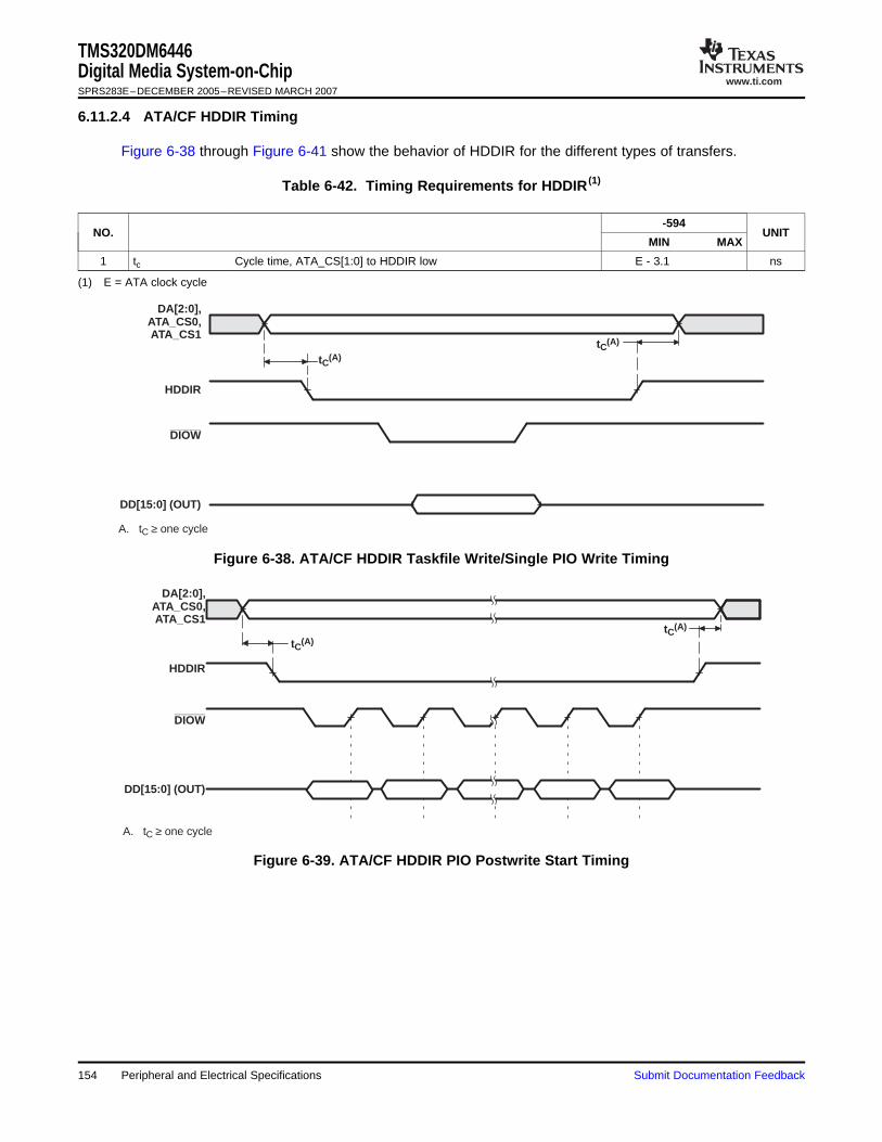
www.ti.com
DA[2:0],ATA_CS0,ATA_CS1
tC(A)
HDDIR
DIOW
DD[15:0] (OUT)
tC(A)
A. tC ≥ one cycle
DA[2:0],ATA_CS0,ATA_CS1
HDDIR
DIOW
DD[15:0] (OUT)
tC(A)
tC(A)
A. tC ≥ one cycle
TMS320DM6446Digital Media System-on-ChipSPRS283E–DECEMBER 2005–REVISED MARCH 2007
6.11.2.4 ATA/CF HDDIR Timing
Figure 6-38 through Figure 6-41 show the behavior of HDDIR for the different types of transfers.
Table 6-42. Timing Requirements for HDDIR (1)
-594NO. UNIT
MIN MAX
1 tc Cycle time, ATA_CS[1:0] to HDDIR low E - 3.1 ns
(1) E = ATA clock cycle
Figure 6-38. ATA/CF HDDIR Taskfile Write/Single PIO Write Timing
Figure 6-39. ATA/CF HDDIR PIO Postwrite Start Timing
Peripheral and Electrical Specifications154 Submit Documentation Feedback

www.ti.com
DA[2:0],ATA_CS0,ATA_CS1
tC(A)
HDDIR
DIOW
DD[15:0] (OUT)
DMACK
tC(A)
A. tC ≥ one cycle
DA[2:0],ATA_CS0,ATA_CS1
HDDIR
DIOW
DD[15:0] (OUT)
DMACK
CRC
tC(A)
A. tC ≥ one cycle
TMS320DM6446Digital Media System-on-Chip
SPRS283E–DECEMBER 2005–REVISED MARCH 2007
Figure 6-40. ATA/CF HDDIR Multiword DMA Write Transfer Timing
Figure 6-41. ATA/CF HDDIR Ultra DMA Write Transfer Timing
Submit Documentation Feedback Peripheral and Electrical Specifications 155

www.ti.com
6.12 MMC/SD/SDIO
6.12.1 MMC/SD/SDIO Peripheral Description(s)
TMS320DM6446Digital Media System-on-ChipSPRS283E–DECEMBER 2005–REVISED MARCH 2007
The DM6446 MMC/SD/SDIO Controller has following features:• MultiMediaCard (MMC).• Secure Digital (SD) memory card with Secure Data I/O (SDIO).• MMC/SD/SDIO protocol support.• Programmable clock frequency.• 256 bit Read/Write FIFO to lower system overhead.• Slave DMA transfer capability.
SDIO is only supported for WLAN operation through TI third parties. For more information aboutthird-party WLAN products, go to http://www.ti.com.davinciwlan.
The MMC/SD/SDIO register memory mapping is shown in Table 6-43.
Table 6-43. MMC/SD/SDIO Register Descriptions
HEX ADDRESS RANGE ACRONYM REGISTER NAME
0x01E1 0000 MMCCTL MMC Control Register
0x01E1 0004 MMCCLK MMC Memory Clock Control Register
0x01E1 0008 MMCST0 MMC Status Register 0
0x01E1 000C MMCST1 MMC Status Register 1
0x01E1 0010 MMCIM MMC Interrupt Mask Register
0x01E1 0014 MMCTOR MMC Response Time-Out Register
0x01E1 0018 MMCTOD MMC Data Read Time-Out Register
0x01E1 001C MMCBLEN MMC Block Length Register
0x01E1 0020 MMCNBLK MMC Number of Blocks Register
0x01E1 0024 MMCNBLC MMC Number of Blocks Counter Register
0x01E1 0028 MMCDRR MMC Data Receive Register
0x01E1 002C MMCDXR MMC Data Transmit Register
0x01E1 0030 MMCCMD MMC Command Register
0x01E1 0034 MMCARGHL MMC Argument Register
0x01E1 0038 MMCRSP01 MMC Response Register 0 and 1
0x01E1 003C MMCRSP23 MMC Response Register 2 and 3
0x01E1 0040 MMCRSP45 MMC Response Register 4 and 5
0x01E1 0044 MMCRSP67 MMC Response Register 6 and 7
0x01E1 0048 MMCDRSP MMC Data Response Register
0x01E1 004C - 0x01E1 004F - Reserved
0x01E1 0050 MMCCIDX MMC Command Index Register
0x01E1 0054 - 0x01E1 0063 - Reserved
0x01E1 0064 - 0x01E1 006C SDIO
0x01E1 0070 - Reserved
0x01E1 0074 MMCFIFOCTL MMC FIFO Control Register
0x01E1 0078 - 0x01E1 FFFF - Reserved
Peripheral and Electrical Specifications156 Submit Documentation Feedback

www.ti.com
6.12.2 MMC/SD/SDIO Electrical Data/Timing
START XMIT Valid Valid Valid END
SD_CLK
SD_CMD
13
79
10
13 13 13
START XMIT Valid Valid Valid END
SD_CLK
SD_CMD
1097
1
2
TMS320DM6446Digital Media System-on-Chip
SPRS283E–DECEMBER 2005–REVISED MARCH 2007
Table 6-44. Timing Requirements for MMC/SD/SDIO Module(see Figure 6-43 and Figure 6-45)
-594
NO. STANDARD MODE UNIT
MIN MAX
1 tsu(CMDV-CLKH) Setup time, SD_CMD valid before SD_CLK high 5 ns
2 th(CLKH-CMDV) Hold time, SD_CMD valid after SD_CLK high 5 ns
3 tsu(DATV-CLKH) Setup time, SD_DATx valid before SD_CLK high 5 ns
4 th(CLKH-DATV) Hold time, SD_DATx valid after SD_CLK high 5 ns
Table 6-45. Switching Characteristics Over Recommended Operating Conditions for MMC/SD/SDIOModule (1) (see Figure 6-42 through Figure 6-45)
-594
NO. PARAMETER STANDARD MODE UNIT
MIN MAX
7 f(CLK) Operating frequency, SD_CLK 0 25 MHz
8 f(CLK_ID) Identification mode frequency, SD_CLK 0 400 KHz
9 tW(CLKL) Pulse width, SD_CLK low 10 ns
10 tW(CLKH) Pulse width, SD_CLK high 10 ns
11 tr(CLK) Rise time, SD_CLK 10 ns
12 tf(CLK) Fall time, SD_CLK 10 ns
13 td(CLKLL-CMD) Delay time, SD_CLK low to SD_CMD transition -7.5 13 ns
14 tdis(CLKL-DAT) Disable time, SD_CLK low to SD_DATx transition -7.5 13 ns
(1) P = Period of SD_CLK (SYSCLK5), in nanoseconds (ns).
Figure 6-42. MMC/SD/SDIO Host Command Timing
Figure 6-43. MMC/SD/SDIO Card Response Timing
Submit Documentation Feedback Peripheral and Electrical Specifications 157

www.ti.com
START D0 D1 Dx END
SD_CLK
SD_DATx
7
1414
910
14 14
Start D0 D1 Dx End
7
SD_CLK
SD_DATx
910
4
3 3
4
TMS320DM6446Digital Media System-on-ChipSPRS283E–DECEMBER 2005–REVISED MARCH 2007
Figure 6-44. MMC/SD/SDIO Host Write Timing
Figure 6-45. MMC/SD/SDIO Host Read and Card CRC Status Timing
158 Peripheral and Electrical Specifications Submit Documentation Feedback

www.ti.com
6.13 Video Processing Sub-System (VPSS) Overview
MHz5795454545.3264
35MHz27 =÷
ø
öçè
æ=-ntscsc
f
MHz4332628318.41017
167MHz27 =÷
ø
öçè
æ=-palscf
TMS320DM6446Digital Media System-on-Chip
SPRS283E–DECEMBER 2005–REVISED MARCH 2007
The DM6446 Video Processing Sub-System (VPSS) provides a Video Processing Front End (VPFE) inputinterface for external imaging peripherals (i.e., image sensors, video decoders, etc.) and a VideoProcessing Back End (VPBE) output interface for display devices, such as analog SDTV displays, digitalLCD panels, HDTV video encoders, etc.
Note: The VPSS module is supported with Linux Application Peripheral Interfaces (APIs) commonly usedby video application developers. Video for Linux 2 or V4L2 uses APIs commonly used for video capture.The typical use cases of the VPSS Video Front-End (VPFE) have been ported to this Linux API structure.V4L2 supports standard video interfaces such as: BT.656 and Y/C mode. Other modules within the VPSSVPFE for example, the Preview Engine, H3A, and Histogram are not currently supported within thesoftware APIs. The VPSS Back-End (VPBE) uses FBDev/DirectFB as the APIs. Certain functionalitieswithin the VPBE have not been implemented in the FBDev/DirectFB APIs. For modes/functions notimplemented in software, it is the user's responsibility to modify the software drivers/APIs.
The VPSS register memory mapping is shown in Table 6-46.
Table 6-46. VPSS Register Descriptions
HEX ADDRESS REGISTER ACRONYM DESCRIPTIONRANGE
0x01C7 3400 PID Peripheral Revision and Class Information
0x01C7 3404 PCR VPSS Control Register
0x01C7 3408 - Reserved
0x01C7 3508 SDR_REG_EXP SDRAM Non Real-Time Read Request Expand
0x01C7 350C - - Reserved0x01C7 3FFF
To ensure NTSC- and PAL-compliant output video, the stability of the input clock source is very important.TI recommends a 27-MHz, 50-ppm crystal. Ceramic oscillators are not recommended. The NTSC/PALcolor sub-carrier frequency is derived from the 27-MHz clock. Therefore, if the 27-MHz clock drifts, thenthe color sub-carrier frequency will drift as well. Assuming no 27-MHz frequency drift, the color sub-carrierfrequency is generated as follows:
To ensure the color sub-carrier frequency will not drift out of spec, the user must follow the crystalrequirements discussed in Section 6.5.1, Clock Input Option 1 – Crystal or Ceramic Resonator.
Submit Documentation Feedback Peripheral and Electrical Specifications 159

www.ti.com
6.13.1 Video Processing Front-End (VPFE)
TMS320DM6446Digital Media System-on-ChipSPRS283E–DECEMBER 2005–REVISED MARCH 2007
The Video Processing Front-End (VPFE) consists of the CCD Controller (CCDC), Preview Engine,Resizer, Hardware 3A (H3A) Statistic Generator, and Histogram blocks. Together, these modules provideDM6446 with a powerful and flexible front-end interface. These modules are briefly described below:• The CCDC provides an interface to image sensors and digital video sources.• The Preview Engine is a parameterized hardwired image processing block which is used for converting
RAW color data from a Bayer pattern to YUV 4:2:2.• The Resizer module re-sizes the input image data to the desired display or video encoding resolution• The H3A module provides control loops for Auto Focus (AF), Auto White Balance (AWB) and Auto
Exposure (AE).• The Histogram module bins input color pixels, depending on the amplitude, and provides statistics
required to implement various 3A (AE/AF/AWB) algorithms and tune the final image/video output.
The VPFE register memory mapping is shown in Table 6-47.
Table 6-47. VPFE Register Address Range Descriptions
HEX ADDRESS RANGE ACRONYM REGISTER NAME
0x01C7 0400 – 0x01C7 07FF CCDC VPFE – CCD Controller
0x01C7 0800 – 0x01C7 0BFF PREV VPFE – Preview Engine/Image Signal Processor
0x01C7 0C00 – 0x01C7 09FF RESZ VPFE – Resizer
0x01C7 1000 – 0x01C7 13FF HIST VPFE – Histogram
0x01C7 1400 – 0x01C7 17FF H3A VPFE – Hardware 3A (Auto-Focus/WB/Exposure)
0x01C7 3400 – 0x01C7 3FFF VPSS VPSS Shared Buffer Logic Registers
6.13.1.1 CCD Controller (CCDC)
The CCDC receives raw image/video data from sensors (CMOS or CCD) or YUV video data in numerousformats from video decoder devices. The following features are supported by the CCDC module.• Conventional Bayer pattern formats.• Generates HD/VD timing signals and field ID to an external timing generator or can synchronize to an
external timing generator.• Interface to progressive and interlaced sensors.• REC656/CCIR-656 standard (YCbCr 4:2:2 format, either 8- or 16-bit).• YCbCr 4:2:2 format, either 8- or 16-bit with discrete H and VSYNC signals.• Up to 16-bit input.• Optical black clamping signal generation.• Shutter signal control.• Digital clamping and black level compensation.• 10-bit to 8-bit A-law compression.• Low-pass filter prior to writing to SDRAM. If this filter is enabled, 2 pixels each in the left and right
edges of each line are cropped from the output.• Output range from 16-bits to 8-bits wide (8-bits wide allows for 50% saving in storage area).• Downsampling via programmable culling patterns.• Control output to the DDR2 via an external write enable signal.• Up to 16K pixels (image size) in both the horizontal and vertical direction.
The CCDC register memory mapping is shown in Table 6-48.
Peripheral and Electrical Specifications160 Submit Documentation Feedback

www.ti.com
TMS320DM6446Digital Media System-on-Chip
SPRS283E–DECEMBER 2005–REVISED MARCH 2007
Table 6-48. CCDC Register Descriptions
HEX ADDRESS RANGE REGISTER ACRONYM DESCRIPTION
0x01C7 0400 PID Peripheral Revision and Class Information
0x01C7 0404 PCR Peripheral Control Register
0x01C7 0408 SYN_MODE SYNC and Mode Set Register
0x01C7 040C HD_VD_WID HD and VD Signal Width
0x01C7 0410 PIX_LINES Number of Pixels in a Horizontal Line and Number of Lines in a Frame
0x01C7 0414 HORZ_INFO Horizontal Pixel Information
0x01C7 0418 VERT_START Vertical Line - Settings for the Starting Pixel
0x01C7 041C VERT_LINES Number of Vertical Lines
0x01C7 0420 CULLING Culling Information in Horizontal and Vertical Directions
0x01C7 0424 HSIZE_OFF Horizontal Size
0x01C7 0428 SDOFST SDRAM/DDRAM Line Offset
0x01C7 042C SDR_ADDR SDRAM Address
0x01C7 0430 CLAMP Optical Black Clamping Settings
0x01C7 0434 DCSUB DC Clamp
0x01C7 0438 COLPTN CCD Color Pattern
0x01C7 043C BLKCMP Black Compensation
0x01C7 0440 - Reserved
0x01C7 0444 - Reserved
0x01C7 0448 VDINT VD Interrupt Timing
0x01C7 044C ALAW A-Law Setting
0x01C7 0450 REC656IF REC656 Interface
0x01C7 0454 CCDCFG CCD Configuration
0x01C7 0458 FMTCFG Data Reformatter/Video Port Configuration
0x01C7 045C FMT_HORZ Data Reformatter/Video Input Interface Horizontal Information
0x01C7 0460 FMT_VERT Data Reformatter/Video Input Interface Vertical Information
0x01C7 0464 FMT_ADDR0 Address Pointer 0 Setup
0x01C7 0468 FMT_ADDR1 Address Pointer 1 Setup
0x01C7 046C FMT_ADDR2 Address Pointer 2 Setup
0x01C7 0470 FMT_ADDR3 Address Pointer 3 Setup
0x01C7 0474 FMT_ADDR4 Address Pointer 4 Setup
0x01C7 0478 FMT_ADDR5 Address Pointer 5 Setup
0x01C7 047C FMT_ADDR6 Address Pointer 6 Setup
0x01C7 0480 FMT_ADDR7 Address Pointer 7 Setup
0x01C7 0484 PRGEVEN_0 Program Entries 0-7 for Even Line
0x01C7 0488 RRGEVEN_1 Program Entries 8-15 for Even Line
0x01C7 048C PRGGODD_0 Program Entries 0-7 for Odd Line
0x01C7 0490 PRGGODD_1 Program Entries 8-15 for Odd Line
0x01C7 0494 VP_OUT Video Port Output Settings
6.13.1.2 Preview Engine
The preview engine transforms raw unprocessed image/video data from a sensor (CMOS or CCD) intoYCbCr 4:2:2 data. The output of the preview engine is used for both video compression and externaldisplay devices such as a NTSC/PAL analog encoder or a digital LCD. The following features aresupported by the preview engine.• Accepts conventional Bayer pattern formats.• Input image/video data from either the CCD/CMOS controller or the DDR2 memory.• Output width up to 1280 pixels wide.
Submit Documentation Feedback Peripheral and Electrical Specifications 161

www.ti.com
TMS320DM6446Digital Media System-on-ChipSPRS283E–DECEMBER 2005–REVISED MARCH 2007
• Automatic/mandatory cropping of pixels/lines when edge processing is performed. If all thecorresponding modules are enabled, a total of 14 pixels per line (7 left most and 7 right most) and 8lines (4 top most and 4 bottom most) will not be output.
• Simple horizontal averaging (by factors of 2, 4, or 8) to handle input widths that are greater than 1280(plus the cropped number) pixels wide.
• Dark frame capture to DDR2.• Dark frame subtraction for every input raw data frame, fetched from DDR2, pixel-by-pixel to improve
video quality.• Lens shading compensation. Each input pixel is multiplied with a corresponding 8-bit gain value and
the result is right shifted by a programmable parameter (0-7 bits).• A-law decompression to transform non-linear 8-bit data to 10-bit linear data. This feature allows data in
DDR2 to be 8-bits, which saves 50% of the area if the input to the preview engine is from the DDR2.• Horizontal median filter for reducing temperature induced noise in pixels.• Programmable noise filter that operates on a 3x3 grid of the same color (effectively, this is a five line
storage requirement).• Digital gain and white balance (color separate gain for white balance).• Programmable CFA interpolation that operates on a 5x5 grid.• Conventional Bayer pattern RGB and complementary color sensors.• Support for an image that is downsampled by 2x in the horizontal direction (with and without phase
correction). In this case, the image is 2/3 populated instead of the conventional 1/3 colors.• Support for an image that is downsampled by 2x in both the horizontal and vertical direction. In this
case, the image is fully populated instead of the conventional 1/3 colors.• Programmable RGB-to-RGB blending matrix (9 coefficients for the 3x3 matrix).• Fully programmable gamma correction (1024 entries for each color held in an on-chip RAM).• Programmable color conversion (RGB to YUV) coefficients (9 coefficients for the 3x3 matrix).• Luminance enhancement (non-linear) and chrominance suppression & offset.
The Preview Engine register memory mapping is shown in Table 6-49.
Table 6-49. Preview Engine Register Descriptions
HEX ADDRESS RANGE REGISTER ACRONYM DESCRIPTION
0x01C7 0800 PID Peripheral Revision and Class Information
0x01C7 0804 PCR Peripheral Control Register
0x01C7 0808 HORZ_INFO Horizontal Information/Setup
0x01C7 080C VERT_INFO Vertical Information/Setup
0x01C7 0810 RSDR_ADDR Read Address From SDRAM
0x01C7 0814 RADR_OFFSET Line Offset for the Read Data
0x01C7 0818 DSDR_ADDR Dark Frame Address From SDRAM
0x01C7 081C DRKF_OFFSET Line Offset for the Dark Frame Data
0x01C7 0820 WSDR_ADDR Write Address to the SDRAM
0x01C7 0824 WADD_OFFSET Line Offset for the Write Data
0x01C7 0828 AVE Input Formatter/Averager
0x01C7 082C HMED Horizontal Median Filter
0x01C7 0830 NF Noise Filter
0x01C7 0834 WB_DGAIN White Balance Digital Gain
0x01C7 0838 WBGAIN White Balance Coefficients
0x01C7 083C WBSEL White Balance Coefficients Selection
0x01C7 0840 CFA CFA Register
0x01C7 0844 BLKADJOFF Black Adjustment Offset
Peripheral and Electrical Specifications162 Submit Documentation Feedback

www.ti.com
TMS320DM6446Digital Media System-on-Chip
SPRS283E–DECEMBER 2005–REVISED MARCH 2007
Table 6-49. Preview Engine Register Descriptions (continued)
HEX ADDRESS RANGE REGISTER ACRONYM DESCRIPTION
0x01C7 0848 RGB_MAT1 RGB2RGB Blending Matrix Coefficients
0x01C7 084C RGB_MAT2 RGB2RGB Blending Matrix Coefficients
0x01C7 0850 RGB_MAT3 RGB2RGB Blending Matrix Coefficients
0x01C7 0854 RGB_MAT4 RGB2RGB Blending Matrix Coefficients
0x01C7 0858 RGB_MAT5 RGB2RGB Blending Matrix Coefficients
0x01C7 085C RGB_OFF1 RGB2RGB Blending Matrix Offsets
0x01C7 0860 RGB_OFF2 RGB2RGB Blending Matrix Offsets
0x01C7 0864 CSC0 Color Space Conversion Coefficients
0x01C7 0868 CSC1 Color Space Conversion Coefficients
0x01C7 086C CSC2 Color Space Conversion Coefficients
0x01C7 0870 CSC_OFFSET Color Space Conversion Offsets
0x01C7 0874 CNT_BRT Contrast and Brightness Settings
0x01C7 0878 CSUP Chrominance Suppression Settings
0x01C7 087C SETUP_YC Maximum/Minimum Y and C Settings
0x01C7 0880 SET_TBL_ADDRESS Setup Table Addresses
0x01C7 0884 SET_TBL_DATA Setup Table Data
6.13.1.3 Resizer
The resizer module can accept input image/video data from either the preview engine or DDR2. Theoutput of the resizer module is sent to DDR2. The following features are supported by the resizer module.• An output width up to 1280 horizontal pixels.• Input from external DDR2.• Up to 4x upsampling (digital zoom).• Bi-cubic interpolation (4-tap horizontal, 4-tap vertical) can be implemented with the programmable filter
coefficients.• 8 phases of filter coefficients.• Optional bi-linear interpolation for the chrominance components.• Up to 1/4x downsampling• 4-tap horizontal and 4-tap vertical filter coefficients (with 8-phases) for 1x to 1/2x downsampling• 1/2x to 1/4x downsampling, for 7-tap mode with 4-phases.• Resizing either YUV 4:2:2 packed data (16-bits) or color separate data (8-bit data within DDR) that is
contiguous.• Separate/independent resizing factor for the horizontal and vertical directions.• Upsampling and downsampling ratios that are available are: 256/N, with N ranging from 64 to 1024.• Programmable luminance sharpening after the horizontal resizing and before the vertical resizing step.
The Resizer register memory mapping is shown in Table 6-50.
Table 6-50. Resizer Register Descriptions
HEX ADDRESS RANGE REGISTER ACRONYM DESCRIPTION
0x01C7 0C00 PID Peripheral Revision and Class Information
0x01C7 0C04 PCR Peripheral Control Register
0x01C7 0C08 RSZ_CNT Resizer Control Bits
0x01C7 0C0C OUT_SIZE Output Width and Height After Resizing
0x01C7 0C10 IN_START Input Starting Information
0x01C7 0C14 IN_SIZE Input Width and Height Before Resizing
Submit Documentation Feedback Peripheral and Electrical Specifications 163

www.ti.com
TMS320DM6446Digital Media System-on-ChipSPRS283E–DECEMBER 2005–REVISED MARCH 2007
Table 6-50. Resizer Register Descriptions (continued)
HEX ADDRESS RANGE REGISTER ACRONYM DESCRIPTION
0x01C7 0C18 SDR_INADD Input SDRAM Address
0x01C7 0C1C SDR_INOFF SDRAM Offset for the Input Line
0x01C7 0C20 SDR_OUTADD Output SDRAM Address
0x01C7 0C24 SDR_OUTOFF SDRAM Offset for the Output Line
0x01C7 0C28 HFILT10 Horizontal Filter Coefficients 1 and 0
0x01C7 0C2C HFILT32 Horizontal Filter Coefficients 3 and 2
0x01C7 0C30 HFILT54 Horizontal Filter Coefficients 5 and 4
0x01C7 0C34 HFILT76 Horizontal Filter Coefficients 7 and 6
0x01C7 0C38 HFILT98 Horizontal Filter Coefficients 9 and 8
0x01C7 0C3C HFILT1110 Horizontal Filter Coefficients 11 and 10
0x01C7 0C40 HFILT1312 Horizontal Filter Coefficients 13 and 12
0x01C7 0C44 HFILT1514 Horizontal Filter Coefficients 15 and 14
0x01C7 0C48 HFILT1716 Horizontal Filter Coefficients 17 and 16
0x01C7 0C4C HFILT1918 Horizontal Filter Coefficients 19 and 18
0x01C7 0C50 HFILT2120 Horizontal Filter Coefficients 21 and 20
0x01C7 0C54 HFILT2322 Horizontal Filter Coefficients 23 and 22
0x01C7 0C58 HFILT2524 Horizontal Filter Coefficients 25 and 24
0x01C7 0C5C HFILT2726 Horizontal Filter Coefficients 27 and 26
0x01C7 0C60 HFILT2928 Horizontal Filter Coefficients 29 and 28
0x01C7 0C64 HFILT3130 Horizontal Filter Coefficients 31 and 30
0x01C7 0C68 VFILT10 Vertical Filter Coefficients 1 and 0
0x01C7 0C6C VFILT32 Vertical Filter Coefficients 3 and 2
0x01C7 0C70 VFILT54 Vertical Filter Coefficients 5 and 4
0x01C7 0C74 VFILT76 Vertical Filter Coefficients 7 and 6
0x01C7 0C78 VFILT98 Vertical Filter Coefficients 9 and 8
0x01C7 0C7C VFILT1110 Vertical Filter Coefficients 11 and 10
0x01C7 0C80 VFILT1312 Vertical Filter Coefficients 13 and 12
0x01C7 0C84 VFILT1514 Vertical Filter Coefficients 15 and 14
0x01C7 0C88 VFILT1716 Vertical Filter Coefficients 17 and 16
0x01C7 0C8C VFILT1918 Vertical Filter Coefficients 19 and 18
0x01C7 0C90 VFILT2120 Vertical Filter Coefficients 21 and 20
0x01C7 0C94 VFILT2322 Vertical Filter Coefficients 23 and 22
0x01C7 0C98 VFILT2524 Vertical Filter Coefficients 25 and 24
0x01C7 0C9C VFILT2726 Vertical Filter Coefficients 27 and 26
0x01C7 0CA0 VFILT2928 Vertical Filter Coefficients 29 and 28
0x01C7 0CA4 VFILT3130 Vertical Filter Coefficients 31 and 30
0x01C7 0CA8 YENH Luminance Enhancer
6.13.1.4 Hardware 3A (H3A)
The Hardware 3A (H3A) module provides control loops for Auto Focus, Auto White Balance and AutoExposure. There are 2 main components of the H3A module:• Auto Focus (AF) Engine• Auto Exposure (AE) & Auto White Balance (AWB) Engine
The AF engine extracts and filters the red, green, and blue data from the input image/video data andprovides either the accumulation or peaks of the data in a specified region. The specified region is a twodimensional block of data and is referred to as a “paxel” for the case of AF.
Peripheral and Electrical Specifications164 Submit Documentation Feedback

www.ti.com
TMS320DM6446Digital Media System-on-Chip
SPRS283E–DECEMBER 2005–REVISED MARCH 2007
The AE/AWB Engine accumulates the values and checks for saturated values in a sub sampling of thevideo data. In the case of the AE/AWB, the two-dimensional block of data is referred to as a “window”.The number, dimensions, and starting position of the AF paxels and the AE/AWB windows are separatelyprogrammable.
The H3A register memory mapping is shown in Table 6-51.
Table 6-51. H3A Register Descriptions
HEX ADDRESS RANGE REGISTER ACRONYM DESCRIPTION
0x01C7 1400 PID Peripheral Revision and Class Information
0x01C7 1404 PCR Peripheral Control Register
0x01C7 1408 AFPAX1 Setup for the AF Engine Paxel Configuration
0x01C7 140C AFPAX2 Setup for the AF Engine Paxel Configuration
0x01C7 1410 AFPAXSTART Start Position for AF Engine Paxels
0x01C7 1414 AFIIRSH Start Position for IIRSH
0x01C7 1418 AFBUFST SDRAM/DDRAM Start Address for AF Engine
0x01C7 141C AFCOEF010 IIR Filter Coefficient Data for SET 0
0x01C7 1420 AFCOEF032 IIR Filter Coefficient Data for SET 0
0x01C7 1424 AFCOEFF054 IIR Filter Coefficient Data for SET 0
0x01C7 1428 AFCOEFF076 IIR Filter Coefficient Data for SET 0
0x01C7 142C AFCOEFF098 IIR Filter Coefficient Data for SET 0
0x01C7 1430 AFCOEFF0010 IIR Filter Coefficient Data for SET 0
0x01C7 1434 AFCOEF110 IIR Filter Coefficient Data for SET 1
0x01C7 1438 AFCOEF132 IIR Filter Coefficient Data for SET 1
0x01C7 143C AFCOEFF154 IIR Filter Coefficient Data for SET 1
0x01C7 1440 AFCOEFF176 IIR Filter Coefficient Data for SET 1
0x01C7 1444 AFCOEFF198 IIR Filter Coefficient Data for SET 1
0x01C7 1448 AFCOEFF1010 IIR Filter Coefficient Data for SET 1
0x01C7 144C AEWWIN1 Configuration for AE/AWB Windows
0x01C7 1450 AEWINSTART Start Position for AE/AWB Windows
0x01C7 1454 AEWINBLK Start Position and Height for Black Line of AE/AWB Windows
0x01C7 1458 AEWSUBWIN Configuration for Subsample Data in AE/AWB Window
0x01C7 145C AEWBUFST SDRAM/DDRAM Start Address for AE/AWB Engine
6.13.1.4.1 Auto Focus (AF) Engine
The following features are supported by the Auto Focus (AF) Engine.• Peak Mode in a Paxel (a Paxel is defined as a two dimensional block of pixels).• Accumulate the maximum Focus Value of each line in a Paxel• Accumulation/Sum Mode (instead of Peak mode).• Accumulate Focus Value in a Paxel.• Up to 36 Paxels in the horizontal direction and up to 128 Paxels in the vertical direction.• Programmable width and height for the Paxel. All paxels in the frame will be of same size.• Programmable red, green, and blue position within a 2x2 matrix.• Separate horizontal start for paxel and filtering.• Programmable vertical line increments within a paxel.• Parallel IIR filters configured in a dual-biquad configuration with individual coefficients (2 filters with 11
coefficients each). The filters are intended to compute the sharpness/peaks in the frame to focus on.
Submit Documentation Feedback Peripheral and Electrical Specifications 165

www.ti.com
TMS320DM6446Digital Media System-on-ChipSPRS283E–DECEMBER 2005–REVISED MARCH 2007
6.13.1.4.2 Auto Exposure (AE) and Auto White Balance (AWB) Engine
The following features are supported by the Auto Exposure (AE) and Auto White Balance (AWB) Engine.• Accumulate clipped pixels along with all non-saturated pixels.• Up to 36 horizontal windows.• Up to 128 vertical windows.• Programmable width and height for the windows. All windows in the frame will be of same size.• Separate vertical start coordinate and height for a black row of paxels that is different than the
remaining color paxels.• Programmable Horizontal Sampling Points in a window.• Programmable Vertical Sampling Points in a window.
6.13.1.5 Histogram
The histogram module accepts raw image/video data and bins the pixels on a value (and color separate)basis. The value of the pixel itself is not stored, but each bin contains the number of pixels that are withinthe appropriate set range. The source of the raw data for the histogram is typically a CCD/CMOS sensor(via the CCDC module) or optionally from DDR2. The following features are supported by the histogrammodule.• Up to four regions/areas.• Separate horizontal/vertical start and end position for each region.• Pixels from overlapping regions are accumulated into the highest priority region. The priority is: region0
> region1 > region2 > region3.• Interface to conventional Bayer pattern. Each region can accumulate either 3 or 4 colors.• 32, 64, 128, or 256 bins per color per region.• 32, 64, or 128 bins per color for 2 regions.• 32 or 64 bins per color for 3 or 4 regions.• Automatic clear of histogram RAM after an ARM read.• Saturation of the pixel count if the count exceeds the maximum value (each memory location is 20-bit
wide).• Downshift ranging from 0 to 7 bits (maximum bin range 128).• The last bin (highest range of values) will accumulate any value that is higher than the lower bound.
The Histogram register memory mapping is shown in Table 6-52.
Table 6-52. Histogram Register Descriptions
HEX ADDRESS RANGE REGISTER ACRONYM DESCRIPTION
0x01C7 1000 PID Peripheral Revision and Class Information Register
0x01C7 1004 PCR Peripheral Control Register
0x01C7 1008 HIST_CNT Histogram Control Bits Register
0x01C7 100C WB_GAIN White/Channel Balance Settings Register
0x01C7 1010 R0_HORZ Region 0 Horizontal Information Register
0x01C7 1014 R0_VERT Region 0 Vertical Information Register
0x01C7 1018 R1_HORZ Region 1 Horizontal Information Register
0x01C7 101C R1_VERT Region 1 Vertical Information Register
0x01C7 1020 R2_HORZ Region 2 Horizontal Information Register
0x01C7 1024 R2_VERT Region 2 Vertical Information Register
0x01C7 1028 R3_HORZ Region 3 Horizontal Information Register
0x01C7 102C R3_VERT Region 3 Vertical Information Register
0x01C7 1030 HIST_ADDR Histogram Address for Data to be Read Register
Peripheral and Electrical Specifications166 Submit Documentation Feedback

www.ti.com
TMS320DM6446Digital Media System-on-Chip
SPRS283E–DECEMBER 2005–REVISED MARCH 2007
Table 6-52. Histogram Register Descriptions (continued)
HEX ADDRESS RANGE REGISTER ACRONYM DESCRIPTION
0x01C7 1034 HIST_DATA Histogram Data That is Read From the Memory Register
0x01C7 1038 RADD Read Address From DDR2 Memory Register
0x01C7 103C RADD_OFF Read Address Offset for Each Line in the DDR2 Memory Register
0x01C7 1040 H_V_INFO Horizontal/Vertical Information Register (Horizontal/Vertical Number ofPixels When Data is Read From DDR2 Memory Information Register)
Submit Documentation Feedback Peripheral and Electrical Specifications 167

www.ti.com
PCLK
2
1
3
44
TMS320DM6446Digital Media System-on-ChipSPRS283E–DECEMBER 2005–REVISED MARCH 2007
6.13.1.6 VPFE Electrical Data/Timing
Table 6-53. Timing Requirements for VPFE PCLK Master/Slave Mode (see Figure 6-46)
-594NO. UNIT
MIN MAX
1 tc(PCLK) Cycle time, PCLK 10.204 or 13.33 (1) 160 ns
2 tw(PCLKH) Pulse duration, PCLK high 4.4 ns
3 tw(PCLKL) Pulse duration, PCLK low 4.4 ns
4 tt(PCLK) Transition time, PCLK 3 ns
(1) When PCLK sources the clock for both the VPFE and VPBE, the minimum cycle time of 13.33 ns (specified in Table 6-60, TimingRequirements for VPBE CLK Inputs for VPBE) must be met. When PCLK sources the clock for only the VPFE, a minimum cycle time of10.2 ns may be used.
Figure 6-46. VPFE PCLK Timing
Table 6-54. Timing Requirements for VPFE (CCD) Slave Mode (1) (see Figure 6-47)
-594NO. UNIT
MIN MAX
5 tsu(CCDV-PCLK) Setup time, CCD valid before PCLK edge 3 ns
6 th(PCLK-CCDV) Hold time, CCD valid after PCLK edge 2 ns
7 tsu(HDV-PCLK) Setup time, HD valid before PCLK edge 3 ns
8 th(PCLK-HDV) Hold time, HD valid after PCLK edge 2 ns
9 tsu(VDV-PCLK) Setup time, VD valid before PCLK edge 3 ns
10 th(PCLK-VDV) Hold time, VD valid after PCLK edge 2 ns
11 tsu(C_WEV-PCLK) Setup time, C_WE valid before PCLK edge 3 ns
12 th(PCLK-C_WEV) Hold time, C_WE valid after PCLK edge 2 ns
13 tsu(C_FIELDV-PCLK) Setup time, C_FIELD valid before PCLK edge 3 ns
14 th(PCLK-C_FIELDV) Hold time, C_FIELD valid after PCLK edge 2 ns
(1) The VPFE may be configured to operate in either positive or negative edge clocking mode. When in positive edge clocking mode therising edge of PCLK is referenced. When in negative edge clocking mode the falling edge of PCLK is referenced.
Peripheral and Electrical Specifications168 Submit Documentation Feedback

www.ti.com
PCLK(Positive Edge Clocking)
PCLK(Negative Edge Clocking)
7, 9
HD/VD
CCD[15:0]
8, 10
11, 13
12, 14
5
6
C_WE/C_FIELD
PCLK(Positive Edge Clocking)
1516
2324
CCD[15:0]
C_WE
PCLK(Negative Edge Clocking)
TMS320DM6446Digital Media System-on-Chip
SPRS283E–DECEMBER 2005–REVISED MARCH 2007
Figure 6-47. VPFE (CCD) Slave Mode Input Data Timing
Table 6-55. Timing Requirements for VPFE (CCD) Master Mode (1) (see Figure 6-48)
-594NO. UNIT
MIN MAX
15 tsu(CCDV-PCLK) Setup time, CCD valid before PCLK edge 3 ns
16 th(PCLK-CCDV) Hold time, CCD valid after PCLK edge 2 ns
23 tsu(CWEV-PCLK) Setup time, C_WE valid before PCLK edge 3 ns
24 th(PCLK-CWEV) Hold time, C_WE valid after PCLK edge 2 ns
(1) The VPFE may be configured to operate in either positive or negative edge clocking mode. When in positive edge clocking mode therising edge of PCLK is referenced. When in negative edge clocking mode the falling edge of PCLK is referenced.
Figure 6-48. VPFE (CCD) Master Mode Input Data Timing
Submit Documentation Feedback Peripheral and Electrical Specifications 169

www.ti.com
PCLK(Negative Edge Clocking)
18
20
22
HD
VD
C_FIELD
PCLK(Positive Edge Clocking)
6.13.2 Video Processing Back-End (VPBE)
TMS320DM6446Digital Media System-on-ChipSPRS283E–DECEMBER 2005–REVISED MARCH 2007
Table 6-56. Switching Characteristics Over Recommended Operating Conditions for VPFE (CCD) MasterMode (1) (see Figure 6-49)
-594NO. PARAMETER UNIT
MIN MAX
18 td(PCLK-HDV) Delay time, PCLK edge to HD valid 0.5 8 ns
20 td(PCLK-VDV) Delay time, PCLK edge to VD valid 0.5 8 ns
22 td(PCLK-C_FIELDV) Delay time, PCLK edge to C_FIELD valid 0.5 8.3 ns
(1) The VPFE may be configured to operate in either positive or negative edge clocking mode. When in positive edge clocking mode therising edge of PCLK is referenced. When in negative edge clocking mode the falling edge of PCLK is referenced.
Figure 6-49. VPFE (CCD) Master Mode Control Output Data Timing
The Video Processing Back-End (VPBE) consists of the On-Screen Display (OSD) module, the VideoEncoder (VENC) including the Digital LCD (DLCD) and Analog (i.e., DAC) interfaces. The video encodergenerates analog video output. The DLCD controller generates digital RGB/YCbCr data output and timingsignals.
The VPBE register memory mapping is shown in Table 6-57.
Table 6-57. VPBE Register Descriptions
Address Register Description
0x01C7 2780 PID Peripheral Revision and Class Information Register
0x01C7 2784 PCR Peripheral Control Register
6.13.2.1 On-Screen Display (OSD)
The major function of the OSD module is to gather and blend video data and display/bitmap data beforefeeding it to the Video Encoder (VENC) in YCbCr format. The video and display data is read from anexternal memory, typically DDR2. The OSD is programmed via control and parameter registers. Thefollowing are the primary features that are supported by the OSD.• Simultaneous display of two video windows and two OSD windows (VIDWIN0/VIDWIN1 and
OSDWIN0/OSDWIN1).– Separate enable for each window– Programmable width, height, and base starting coordinates for each window– External memory address and offset registers for each window– Support for x2 and x4 zoom in both the horizontal and vertical direction– OSDWIN1 can be used as an attribute window for OSDWIN0
Peripheral and Electrical Specifications170 Submit Documentation Feedback

www.ti.com
TMS320DM6446Digital Media System-on-Chip
SPRS283E–DECEMBER 2005–REVISED MARCH 2007
– Attribute window blinking intervals– Field/frame mode for the windows (interlaced/progressive)– Eight step blending process between the OSD and video windows– Transparency support for the OSD and video data (when a bitmap pixel is zero, there will be no
blending for that corresponding video pixel)– Resize from VGA to NTSC/PAL (640x480 to 720x576) for both the OSD and video windows– Reads in YCbCr data in 4:2:2 format from external memory, with the capability for swapping the
order of the CbCr component in the 32-bit word (this is relevant to the two video windows)– Support for a ping-pong buffer scheme that can be used for VIDWIN0 (allows for video data to be
accessed from two different locations in DDR2)– Each OSD window (either one, but not both at the same time) is capable of reading in RGB data
(16-bit data with six bits for the green and five bits each for the red and blue colors) instead ofbitmap data in YCbCr format restricted to a maximum of 8-bits
– The OSD bitmap data width is selectable between 1, 2, 4, or 8-bits.– Each OSD window supports 16 entries for the bitmap (to index into a 256 entry RAM/ROM CLUT
table).– Indirect support for 24-bit RGB input data (which will be transformed into 16-bit YCbCr video
window data) via the wrapper interface in the VPBE.• Support for a rectangular cursor window and a programmable background color selection.
– Programmable color palette with the ability to select between a RAM/ROM table with support for256 colors.
– The width, height, and color of the cursor is programmable.– The display priority is: Rectangular-Cursor > OSDWIN1 > OSDWIN0 > VIDWIN1 > VIDWIN0 >
background color• Support for attenuation of the YCbCr values for the REC601 standard.
The following restrictions exist in the OSD module.• Both the OSD windows and VIDWIN1 should be fully contained inside VIDWIN0.• When one of the OSD windows is set in RGB mode, it cannot overlap with VIDWIN1.• The OSD cannot support more than 256 color entries in the CLUT RAM/ROM. Some applications
require higher number of entries, and one workaround is to use VIDWIN1 as an overlay mimicking theOSD window. Another option is to use the RGB mode for one of the OSD windows which allows for atotal of 16-bits for the R, G, and B colors (64K colors).
• The OSD can only read YCbCr in 4:2:2 interleaved format for the video windows. Other formats, eithercolor separate storage or 4:4:4/4:2:0 interleaved data is not supported.
• If the vertical resize filter is enabled for either of the video windows, the maximum horizontal windowdimension cannot be greater than 720 currently.
• It is not possible to use both of the CLUT ROMs at the same time. However, one window can useRAM while another uses ROM.
• The 24-bit RGB input mode is only valid for one of the two video windows (programmable) and doesnot apply to the OSD windows.
The OSD register memory mapping is shown in Table 6-58.
Table 6-58. OSD Register Descriptions
Address Register Description
0x01C7 2600 MODE OSD Mode Register
0x01C7 2604 VIDWINMD Video Window Mode Setup
0x01C7 2608 OSDWIN0MD OSD Window Mode Setup
0x01C7 260C OSDWIN1MD OSD Window 1 Mode Setup (when used as a second OSD window)
Submit Documentation Feedback Peripheral and Electrical Specifications 171

www.ti.com
TMS320DM6446Digital Media System-on-ChipSPRS283E–DECEMBER 2005–REVISED MARCH 2007
Table 6-58. OSD Register Descriptions (continued)
0x01C7 260C OSDATRMD OSD Attribute Window Mode Setup (when used as an attribute window)
0x01C7 2610 RECTCUR Rectangular Cursor Setup
0x01C7 2614 RSV0 Reserved
0x01C7 2618 VIDWIN0OFST Video Window 0 Offset
0x01C7 261C VIDWIN1OFST Video Window 1 Offset
0x01C7 2620 OSDWIN0OFST OSD Window 0 Offset
0x01C7 2624 OSDWIN1OFST OSD Window 1 Offset
0x01C7 2628 RSV1 Reserved
0x01C7 262C VIDWIN0ADR Video Window 0 Address
0x01C7 2630 VIDWIN1ADR Video Window 1 Address
0x01C7 2634 RSV2 Reserved
0x01C7 2638 OSDWIN0ADR OSD Window 0 Address
0x01C7 263C OSDWIN1ADR OSD Window 1 Address
0x01C7 2640 BASEPX Base Pixel X
0x01C7 2644 BASEPY Base Pixel Y
0x01C7 2648 VIDWIN0XP Video Window 0 X-Position
0x01C7 264C VIDWIN0YP Video Window 0 Y-Position
0x01C7 2650 VIDWIN0XL Video Window 0 X-Size
0x01C7 2654 VIDWIN0YL Video Window 0 Y-Size
0x01C7 2658 VIDWIN1XP Video Window 1 X-Position
0x01C7 265C VIDWIN1YP Video Window 1 Y-Position
0x01C7 2660 VIDWIN1XL Video Window 1 X-Size
0x01C7 2664 VIDWIN1YL Video Window 1 Y-Size
0x01C7 2668 OSDWIN0XP OSD Bitmap Window 0 X-Position
0x01C7 266C OSDWIN0YP OSD Bitmap Window 0 Y-Position
0x01C7 2670 OSDWIN0XL OSD Bitmap Window 0 X-Size
0x01C7 2674 OSDWIN0YL OSD Bitmap Window 0 Y-Size
0x01C7 2678 OSDWIN1XP OSD Bitmap Window 1 X-Position
0x01C7 267C OSDWIN1YP OSD Bitmap Window 1 Y-Position
0x01C7 2680 OSDWIN1XL OSD Bitmap Window 1 X-Size
0x01C7 2684 OSDWIN1YL OSD Bitmap Window 1 Y-Size
0x01C7 2688 CURXP Rectangular Cursor Window X-Position
0x01C7 268C CURYP Rectangular Cursor Window Y-Position
0x01C7 2690 CURXL Rectangular Cursor Window X-Size
0x01C7 2694 CURYL Rectangular Cursor Window Y-Size
0x01C7 2698 RSV3 Reserved
0x01C7 269C RSV4 Reserved
0x01C7 26A0 W0BMP01 Window 0 Bitmap Value to Palette Map 0/1
0x01C7 26A4 W0BMP23 Window 0 Bitmap Value to Palette Map 2/3
0x01C7 26A8 W0BMP45 Window 0 Bitmap Value to Palette Map 4/5
0x01C7 26AC W0BMP67 Window 0 Bitmap Value to Palette Map 6/7
0x01C7 26B0 W0BMP89 Window 0 Bitmap Value to Palette Map 8/9
0x01C7 26B4 W0BMPAB Window 0 Bitmap Value to Palette Map A/B
0x01C7 26B8 W0BMPCD Window 0 Bitmap Value to Palette Map C/D
0x01C7 26BC W0BMPEF Window 0 Bitmap Value to Palette Map E/F
0x01C7 26C0 W1BMP01 Window 1 Bitmap Value to Palette Map 0/1
0x01C7 26C4 W1BMP23 Window 1 Bitmap Value to Palette Map 2/3
0x01C7 26C8 W1BMP45 Window 1 Bitmap Value to Palette Map 4/5
Peripheral and Electrical Specifications172 Submit Documentation Feedback

www.ti.com
TMS320DM6446Digital Media System-on-Chip
SPRS283E–DECEMBER 2005–REVISED MARCH 2007
Table 6-58. OSD Register Descriptions (continued)
0x01C7 26CC W1BMP67 Window 1 Bitmap Value to Palette Map 6/7
0x01C7 26D0 W1BMP89 Window 1 Bitmap Value to Palette Map 8/9
0x01C7 26D4 W1BMPAB Window 1 Bitmap Value to Palette Map A/B
0x01C7 26D8 W1BMPCD Window 1 Bitmap Value to Palette Map C/D
0x01C7 26DC W1BMPEF Window 1 Bitmap Value to Palette Map E/F
0x01C7 26E0 - Reserved
0x01C7 26E4 RSV5 Reserved
0x01C7 26E8 MISCCTL Miscellaneous Control
0x01C7 26EC CLUTRAMYCB CLUT RAMYCB Setup
0x01C7 26F0 CLUTRAMCR CLUT RAM Setup
0x01C7 26F4 TRANSPVAL CLUT RAM Setup
0x01C7 26F8 RSV6 Reserved
0x01C7 26FC PPVWIN0ADR Ping-Pong Video Window 0 Address
6.13.2.2 Video Encoder (VENC)
Analog/DACs interface of the Video Encoder (VENC) supports the following features.• Master Clock Input - 27MHz (x2 Upsampling)• SDTV Support
– Composite NTSC-M, PAL-B/D/G/H/I– S-Video (Y/C)– Component YPbPr (SMPTE/EBU N10, Betacam, MII)– RGB– Non-Interlace– CGMS/WSS– Line 21 Closed Caption Data Encoding– Chroma Low Pass Filter 1.5MHz/3MHz– Programmable SC-H phase
• HDTV Support– Progressive Output (525p/625p)– Component YPbPr– RGB– CGMS/WSS
• 4 10-bit Over-Sampling D/A Converters• Optional 7.5% Pedestal• 16-235/0-255 Input Amplitude Selectable• Programmable Luma Delay• Master/Slave Operation• Internal Color Bar Generation (100%/75%)
The Digital LCD Controller (DLCD) of the VENC supports the following features.• Programmable DCLK• Various Output Formats
– YCbCr 16bit– YCbCr 8bit– ITU-R BT. 656– Parallel RGB 24bit
• Low Pass Filter for Digital RGB Output
Submit Documentation Feedback Peripheral and Electrical Specifications 173

www.ti.com
TMS320DM6446Digital Media System-on-ChipSPRS283E–DECEMBER 2005–REVISED MARCH 2007
• Programmable Timing Generator• Master/Slave Operation• Internal Color Bar Generation (100%/75%)
The VENC register memory mapping including the Digital LCD and DACs is shown in Table 6-59.
Table 6-59. VENC (Including Digital LCD and DACs) Register Descriptions
Address Register Description
0x01C7 2400 VMOD Video Mode
0x01C7 2404 VIDCTL Video Interface I/O Control
0x01C7 2408 VDPRO Video Data Processing
0x01C7 240C SYNCCTL Sync Control
0x01C7 2410 HSPLS Horizontal Sync Pulse Width
0x01C7 2414 VSPLS Vertical Sync Pulse Width
0x01C7 2418 HINT Horizontal Interval
0x01C7 241C HSTART Horizontal Valid Data Start Position
0x01C7 2420 HVALID Horizontal Data Valid Range
0x01C7 2424 VINT Vertical Interval
0x01C7 2428 VSTART Vertical Valid Data Start Position
0x01C7 242C VVALID Vertical Data Valid Range
0x01C7 2430 HSDLY Horizontal Sync Delay
0x01C7 2434 VSDLY Vertical Sync Delay
0x01C7 2438 YCCTL YCbCr Control
0x01C7 243C RGBCTL RGB Control
0x01C7 2440 RGBCLP RGB Level Clipping
0x01C7 2444 LINECTL Line ID Control
0x01C7 2448 CULLLINE Culling Line Control
0x01C7 244C LCDOUT LCD Output Signal Control
0x01C7 2450 BRTS Brightness Start Position Signal Control
0x01C7 2454 BRTW Brightness Width Signal Control
0x01C7 2458 ACCTL LCD_AC Signal Control
0x01C7 245C PWMP PWM Start Position Signal Control
0x01C7 2460 PWMW PWM Width Signal Control
0x01C7 2464 DCLKCTL DCLK Control
0x01C7 2468 DCLKPTN0 DCLK Pattern 0
0x01C7 246C DCLKPTN1 DCLK Pattern 1
0x01C7 2470 DCLKPTN2 DCLK Pattern 2
0x01C7 2474 DCLKPTN3 DCLK Pattern 3
0x01C7 2478 DCLKPTN0A DCLK Auxiliary Pattern 0
0x01C7 247C DCLKPTN1A DCLK Auxiliary Pattern 1
0x01C7 2480 DCLKPTN2A DCLK Auxiliary Pattern 2
0x01C7 2484 DCLKPTN3A DCLK Auxiliary Pattern 3
0x01C7 2488 DCLKHS Horizontal DCLK Mask Start
0x01C7 248C DCLKHSA Horizontal Auxiliary DCLK Mask Start
0x01C7 2490 DCLKHR Horizontal DCLK Mask Range
0x01C7 2494 DCLKVS Vertical DCLK Mask Start
0x01C7 2498 DCLKVR Vertical DCLK Mask Range
0x01C7 249C CAPCTL Caption Control
0x01C7 24A0 CAPDO Caption Data Odd Field
Peripheral and Electrical Specifications174 Submit Documentation Feedback

www.ti.com
TMS320DM6446Digital Media System-on-Chip
SPRS283E–DECEMBER 2005–REVISED MARCH 2007
Table 6-59. VENC (Including Digital LCD and DACs) Register Descriptions (continued)
0x01C7 24A4 CAPDE Caption Data Even Field
0x01C7 24A8 ATR0 Video Attribute Data # 0
0x01C7 24AC ATR1 Video Attribute Data # 1
0x01C7 24B0 ATR2 Video Attribute Data # 2
0x01C7 24B4
0x01C7 24B4Reserved
0x01C7 24B4
0x01C7 24B4
0x01C7 24B8 VSTAT Video Status
0x01C7 24BCReserved
0x01C7 24C0
0x01C7 24C4 DACTST DAC Test
0x01C7 24C8 YCOLVL YOUT and COUT Levels
0x01C7 24CC SCPROG Sub-Carrier Programming
0x01C7 24D0
0x01C7 24D4 Reserved
0x01C7 24D8
0x01C7 24DC CVBS Composite Mode
0x01C7 24E0 CMPNT Component Mode
0x01C7 24E4 ETMG0 CVBS Timing Control 0
0x01C7 24E8 ETMG1 CVBS Timing Control 1
0x01C7 24EC ETMG2 Component Timing Control 0
0x01C7 24F0 ETMG3 Component Timing Control 1
0x01C7 24F4 DACSEL DAC Output Select
0x01C7 24F8Reserved
0x01C7 24FC
0x01C7 2500 ARGBX0 Analog RGB Matrix 0
0x01C7 2504 ARGBX1 Analog RGB Matrix 1
0x01C7 2508 ARGBX2 Analog RGB Matrix 2
0x01C7 250C ARGBX3 Analog RGB Matrix 3
0x01C7 2510 ARGBX4 Analog RGB Matrix 4
0x01C7 2514 DRGBX0 Digital RGB Matrix 0
0x01C7 2518 DRGBX1 Digital RGB Matrix 1
0x01C7 251C DRGBX2 Digital RGB Matrix 2
0x01C7 2520 DRGBX3 Digital RGB Matrix 3
0x01C7 2524 DRGBX4 Digital RGB Matrix 4
0x01C7 2528 VSTARTA Vertical Data Valid Start Position for Even Field
0x01C7 252C OSDCLK0 OSD Clock Control 0
0x01C7 2530 OSDCLK1 OSD Clock Control 1
0x01C7 2534 HVLDCL0 Horizontal Valid Culling Control 0
0x01C7 2538 HVLDCL1 Horizontal Valid Culling Control 1
0x01C7 253C OSDHADV OSD Horizontal Sync Advance
Submit Documentation Feedback Peripheral and Electrical Specifications 175

www.ti.com
1
PCLK
2
3
75
64
8
VPBECLK
4
8
TMS320DM6446Digital Media System-on-ChipSPRS283E–DECEMBER 2005–REVISED MARCH 2007
6.13.2.3 VPBE Electrical Data/Timing
Table 6-60. Timing Requirements for VPBE CLK Inputs (see Figure 6-50)
-594NO. UNIT
MIN MAX
1 tc(PCLK) Cycle time, PCLK 13.33 160 ns
2 tw(PCLKH) Pulse duration, PCLK high 5.7 ns
3 tw(PCLKL) Pulse duration, PCLK low 5.7 ns
4 tt(PCLK) Transition time, PCLK 3 ns
5 tc(VPBECLK) Cycle time, VPBECLK 13.33 160 ns
6 tw(VPBECLKH) Pulse duration, VPBECLK high 5.7 ns
7 tw(VPBECLKL) Pulse duration, VPBECLK low 5.7 ns
8 tt(VPBECLK) Transition time, VPBECLK 3 ns
Figure 6-50. VPBE PCLK and VPBECLK Timing
176 Peripheral and Electrical Specifications Submit Documentation Feedback

www.ti.com
PCLK(Positive Edge Clocking)
9
PCLK(Negative Edge Clocking)
10
VCTL(A)
A. VCTL = HSYNC and VSYNC
VPBECLK
2728
3334
3536
LCD_FIELD
TMS320DM6446Digital Media System-on-Chip
SPRS283E–DECEMBER 2005–REVISED MARCH 2007
Table 6-61. Timing Requirements for VPBE Control Input With Respect to PCLK and VPBECLK (1) (seeFigure 6-51)
-594NO. UNIT
MIN MAX
9 tsu(VCTLV-PCLK) Setup time, VCTL valid before PCLK edge 2 ns
10 th(PCLK-VCTLV) Hold time, VCTL valid after PCLK edge 0.5 ns
27 tsu(VCTLV-VPBECLK) Setup time, VCTL valid before VPBECLK rising edge 2 ns
28 th(VPBECLK-VCTLV) Hold time, VCTL valid after VPBECLK rising edge 0.5 ns
33 tsu(FIELD-PCLK) Setup time, LCD_FIELD valid before PCLK edge 5P (2) ns
34 th(PCLK-FIELD) Hold time, LCD_FIELD valid after PCLK edge 5P (2) ns
35 tsu(FIELD-VPBECLK) Setup time, LCD_FIELD valid before VPBECLK edge 5P (2) ns
36 th(VPBECLK-FIELD) Hold time, LCD_FIELD valid after VPBECLK edge 5P (2) ns
(1) PCLK may be configured to operate in either positive or negative edge clocking mode. When in positive edge clocking mode, the risingedge of PCLK is referenced. When in negative edge clocking mode, the falling edge of PCLK is referenced.
(2) P = 1/(VCLKIN clock frequency) in ns. VCLKIN is either PCLK or VPBECLK, whichever is used.
Figure 6-51. VPBE Input Timing With Respect to PCLK and VPBECLK
Submit Documentation Feedback Peripheral and Electrical Specifications 177

www.ti.com
PCLK(Positive Edge Clocking)
13, 31
PCLK(Negative Edge Clocking)
11, 29
VCTL(A)
A. VCTL = HSYNC, VSYNC, LCD_FIELD, and LCD_OEB. VDATA = COUT[7:0], YOUT[7:0], R[7:0], G[7:0], and B[7:0]
VDATA(B)14, 32
12, 30
VPBECLK
TMS320DM6446Digital Media System-on-ChipSPRS283E–DECEMBER 2005–REVISED MARCH 2007
Table 6-62. Switching Characteristics Over Recommended Operating Conditions for VPBE Control andData Output With Respect to PCLK and VPBECLK (1) (see Figure 6-52)
-594NO. PARAMETER UNIT
MIN MAX
11 td(PCLK-VCTLV) Delay time, PCLK edge to VCTL valid 13.3 ns
12 td(PCLK-VCTLIV) Delay time, PCLK edge to VCTL invalid 2 ns
13 td(PCLK-VDATAV) Delay time, PCLK edge to VDATA valid 13.3 ns
14 td(PCLK-VDATAIV) Delay time, PCLK edge to VDATA invalid 2 ns
29 td(VPBECLK-VCTLV) Delay time, VPBECLK rising edge to VCTL valid 13.3 ns
30 td(VPBECLK-VCTLIV) Delay time, VPBECLK rising edge to VCTL invalid 2 ns
31 td(VPBECLK-VDATAV) Delay time, VPBECLK rising edge to VDATA valid 13.3 ns
32 td(VPBECLK-VDATAIV) Delay time, VPBECLK rising edge to VDATA invalid 2 ns
(1) PCLK may be configured to operate in either positive or negative edge clocking mode. When in positive edge clocking mode, the risingedge of PCLK is referenced. When in negative edge clocking mode, the falling edge of PCLK is referenced.
Figure 6-52. VPBE Output Timing With Respect to PCLK and VPBECLK
Peripheral and Electrical Specifications178 Submit Documentation Feedback

www.ti.com
VCLK(Positive Edge
Clocking)VCLK
(Negative EdgeClocking)
17
VCTL(B)
VDATA(C)
181922
21
23 24
25 26
VCLKIN(A)
A. VCLKIN = PCLK or VPBECLKB. VCTL = HSYNC, VSYNC, LCD_FIELD, and LCD_OEC. VDATA = COUT[7:0], YOUT[7:0], R[7:0], G[7:0], and B[7:0]
2020
TMS320DM6446Digital Media System-on-Chip
SPRS283E–DECEMBER 2005–REVISED MARCH 2007
Table 6-63. Switching Characteristics Over Recommended Operating Conditions for VPBE Control andData Output With Respect to VCLK (1) (2) (see Figure 6-53)
-594NO. PARAMETER UNIT
MIN MAX
17 tc(VCLK) Cycle time, VCLK 13.33 160 ns
Pulse duration, VCLK high (positive-edge clocking) H - 1.3 (3) H - 0.3 (3) ns18 tw(VCLKH)
Pulse duration, VCLK high (negative-edge clocking) L - 1.3 (3) L - 0.3 (3)
Pulse duration, VCLK low (positive-edge clocking) L + 0.3 (3) L + 1.3 (3) ns19 tw(VCLKL)
Pulse duration, VCLK low (negative-edge clocking) H + 0.3 (3) H + 1.3 (3)
20 tt(VCLK) Transition time, VCLK 3 ns
21 td(VCLKINH-VCLKH) Delay time, VCLKIN high to VCLK high 2 12 ns
22 td(VCLKINL-VCLKL) Delay time, VCLKIN low to VCTL low 2 12 ns
23 td(VCLK-VCTLV) Delay time, VCLK edge to VCTL valid 4 ns
24 td(VCLKL-VCTLIV) Delay time, VCLK edge to VCTL invalid 0 ns
25 td(VCLK-VDATAV) Delay time, VCLK edge to VDATA valid 4 ns
26 td(VCLKL-VDATAIV) Delay time, VCLK edge to VDATA invalid 0 ns
(1) The VPBE may be configured to operate in either positive or negative edge clocking mode. When in positive edge clocking mode, therising edge of VCLK is referenced. When in negative edge clocking mode, the falling edge of VCLK is referenced.
(2) VCLKIN = PCLK or VPBECLK(3) H and L are the high and low pulse widths of the input clock to the VPBE, respectively. For example, if VPBECLK is used as the input
clock and it has a high pulse duration of 6.67 ns, the resulting high pulse duration of VCLK, if positive-edge clocking is selected, will be aMAX of 6.37 ns and a MIN of 5.27 ns.
Figure 6-53. VPBE Control and Data Output Timing With Respect to VCLK
Submit Documentation Feedback Peripheral and Electrical Specifications 179

www.ti.com
TMS320DM6446Digital Media System-on-ChipSPRS283E–DECEMBER 2005–REVISED MARCH 2007
6.13.2.4 DAC Electrical Data/Timing
Table 6-64. Switching Characteristics Over Recommended Operating Conditions for DAC StaticSpecifications
-594NO. PARAMETER TEST CONDITIONS UNIT
MIN TYP MAX
DC Accuracy -1.0 1.0 LSBIntegral Non-Linearity (INL) -0.5 0.5 LSBDifferential Non-Linearity (DNL)
Analog Output 0.5 LSBOffset Error 5 %FSGain Error 500 mVPPFull-Scale Output Voltage RLOAD = 500 Ω
Output Capacitance 200 pF
Reference 0.475 0.5 0.525 VReference Voltage Range (VREF) 3.8 4.0 4.2 kΩFull-Scale Current Adjust Resistor (RBIAS)
Table 6-65. Switching Characteristics Over Recommended Operating Conditions for DAC DynamicSpecifications
-594NO. PARAMETER TEST CONDITIONS UNIT
MIN TYP MAX
Output Update Rate (FCLK) 27 60 MHz
Signal Bandwidth 6 MHz
FCLK = 27 MHz60 dB
FOUT = 2.0 MHzSFDR to Nyquist
FCLK = 60 MHz60 dB
FOUT = 2.0 MHz
FCLK = 27 MHz60 db
FOUT = 2.0 MHzSFDR within Bandwidth
FCLK = 60 MHz60 dB
FOUT = 2.0 MHz
PSRR Over Temp vs Power Supply 50 dB
Peripheral and Electrical Specifications180 Submit Documentation Feedback

www.ti.com
Low-Pass Filter
= 6.5 MHz
~R = 500
fc
LOADΩ
3.3 V
DAC−
+ 75 Ω
75 Ω
R2 = 1.12 kΩ
R1 = 267 Ω
LO A Dout
1
2O RI
R
R1V ´´÷
÷ø
öççè
æ+=
VO
TMS320DM6446Digital Media System-on-Chip
SPRS283E–DECEMBER 2005–REVISED MARCH 2007
The DM6446's analog video DAC outputs are designed to drive a 500-Ω load. Figure 6-54 describes atypical circuit that will permit connecting the analog video output from the DM6446 device to standard75-Ω impedance video systems. Another solution is to use a Video Amplifier, such as the TexasInstruments' OPA361, which provides a complete solution to the typical output circuit shown inFigure 6-54.
Figure 6-54. Typical Output Circuit for NTSC/PAL Video From DACs
Submit Documentation Feedback Peripheral and Electrical Specifications 181

www.ti.com
6.14 Host-Port Interface (HPI)
TMS320DM6446Digital Media System-on-ChipSPRS283E–DECEMBER 2005–REVISED MARCH 2007
The Host Port Interface (HPI) provides a parallel port through which an external host processor canaccess the DM6446 memory space. The host device is asynchronous to the DM6446 clocks and functionsas a master to the HPI interface. The HPI enables a host device and DM6446 to exchange information viainternal or external memory. Both the host and DM6446 can access the HPI control register (HPIC) andthe HPI address registers (HPIAR, HPIAW). The host can access the HPI data register (HPID) and theHPIC by using the external data and interface control signals.
The HPI interface shares the DaVinci EMIFA 16-bit data bus pins for multiplexed address/data andsupports the following modes:• 16 Bit Multiplexed mode / dual half-word cycles (16 bit host data bus/32 bit memory width)• ARM ROM supports booting of DM6446 ARM processor from an external processor
The HPI registers are summarized in Table 6-66. For more detailed information on the HPI peripheral, seethe Documentation Support section for the Host Port Interface (HPI) Reference Guide.
Table 6-66. Host-Port Interface (HPI) Register Descriptions
HEX ADDRESS RANGE ACRONYM REGISTER NAME
0x01C4 0030 HPI_CTL Host-Port Interface Configuration Register
0x01C6 7800 HPI_PID
0x01C6 7804 HPIPWREMU HPI Power and Emulation Management Register
0x01C6 7808 - 0x01C6 782F – Reserved
0x01C6 7830 HPIC Host-Port Interface Control Register
0x01C6 7834 HPIAW Host-Port Interface Write Address Register
0x01C6 7838 HPIAR Host-Port Interface Read Address Register
0x01C6 783C - 0x01C6 7FFF – Reserved
The HPI_CTL register sets the owner of HPIA(R/W) and HPIC registers for HPI address and control. Thedetails for HPI_CTL are shown in Figure 6-55 and Table 6-67.
Figure 6-55. HPI_CTL Register
31 30 29 28 27 26 25 24 23 22 21 20 19 18 17 16
Reserved
R-0000000000000000
15 14 13 12 11 10 9 8 7 6 5 4 3 2 1 0
CTL ADDReserved TIMOUTMODE MODE
R-0 R/W-0 R/W-0 R/W-10000000
LEGEND: R = Read, W = Write, n = value at reset
Table 6-67. HPI_CTL Register Description
Name Description
CTLMODE HPIC register write access0 = External Host1 = DM6446 (if ADDMODE = 1)
ADDMODE HPIA register write access0 = External Host1 = DM6446
TIMOUT Host burst write timeout value
Peripheral and Electrical Specifications182 Submit Documentation Feedback

www.ti.com
6.14.1 Host-Port Interface (HPI) Electrical Data/Timing
TMS320DM6446Digital Media System-on-Chip
SPRS283E–DECEMBER 2005–REVISED MARCH 2007
Table 6-68. Timing Requirements for Host-Port Interface Cycles (1) (2) (see Figure 6-56 through Figure 6-57)
-594NO. UNIT
MIN MAX
1 tsu(SELV-HSTBL) Setup time, select signals (3) valid before HSTROBE low 5 ns
2 th(HSTBL-SELV) Hold time, select signals (3) valid after HSTROBE low 2 ns
3 tw(HSTBL) Pulse duration, HSTROBE low 15 ns
4 tw(HSTBH) Pulse duration, HSTROBE high between consecutive accesses 2P ns
12 tsu(HDV-HSTBH) Setup time, host data valid before HSTROBE high 5 ns
13 th(HSTBH-HDV) Hold time, host data valid after HSTROBE high 0 ns
Hold time, HSTROBE high after HRDY low. HSTROBE should not be14 th(HRDYL-HSTBH) inactivated until HRDY is active (low); otherwise, HPI writes will not complete 2 ns
properly.
(1) HSTROBE refers to the following logical operation on HCS, HDS1, and HDS2: [NOT(HDS1 XOR HDS2)] OR HCS.(2) P = 1/CPU clock frequency in ns. For example, when running parts at 594 MHz, use P = 1.68 ns.(3) Select signals include: HCNTL[1:0] and HR/W. For HPI16 mode only, select signals also include HHWIL.
Table 6-69. Switching Characteristics Over Recommended Operating Conditions During Host-PortInterface Cycles (1) (see Figure 6-56 through Figure 6-57)
-594NO. PARAMETER UNIT
MIN MAX
6 td(HSTBL-HRDYH) Delay time, HSTROBE low to HRDY high (2) 0 12 ns
7 td(HSTBL-HDLZ) Delay time, HSTROBE low to HD low impedance for an HPI read 0 ns
8 td(HDV-HRDYL) Delay time, HD valid to HRDY low 0 ns
9 toh(HSTBH-HDV) Output hold time, HD valid after HSTROBE high 1.5 ns
15 td(HSTBH-HDHZ) Delay time, HSTROBE high to HD high impedance 7 ns
Delay time, HSTROBE low to HD valid (HPI16 mode, 2nd half-word16 td(HSTBL-HDV) 15 nsonly)
20 td(HCSL-HRDYH) Delay time, HCS low to HRDY high 0 12 ns
(1) HSTROBE refers to the following logical operation on HCS, HDS1, and HDS2: [NOT(HDS1 XOR HDS2)] OR HCS.(2) This parameter is used during HPID reads and writes. For reads, at the beginning of the first half-word transfer (HPI16) on the falling
edge of HSTROBE, the HPI sends the request to the EDMA internal address generation hardware, and HRDY remains high until theEDMA internal address generation hardware loads the requested data into HPID. For writes, HRDY goes high if the internal write bufferis full.
Submit Documentation Feedback Peripheral and Electrical Specifications 183

www.ti.com
1st half-word 2nd half-word86
15916
1597
43
21
21
21
21
21
21
HCNTL[1:0]
HR/W
HHWIL
HSTROBE(A)
HCS
HD[15:0] (output)
HRDY
3
20
1st half-word 2nd half-word
1312
1312
4
14
3
21
21
21
21
21
21
HCNTL[1:0]
HR/W
HHWIL
HSTROBE(A)
HCS
HD[15:0] (input)
HRDY
3
620
TMS320DM6446Digital Media System-on-ChipSPRS283E–DECEMBER 2005–REVISED MARCH 2007
A. HSTROBE refers to the following logical operation on HCS, HDS1, and HDS2: [NOT(HDS1 XOR HDS2)] OR HCS.
Figure 6-56. HPI16 Read Timing
A. HSTROBE refers to the following logical operation on HCS, HDS1, and HDS2: [NOT(HDS1 XOR HDS2)] OR HCS.
Figure 6-57. HPI16 Write Timing
184 Peripheral and Electrical Specifications Submit Documentation Feedback

www.ti.com
6.15 USB 2.0
6.15.1 USBPHY_CTL Register Description
TMS320DM6446Digital Media System-on-Chip
SPRS283E–DECEMBER 2005–REVISED MARCH 2007
The DM6446 USB2.0 peripheral supports the following features:• USB 2.0 peripheral at speeds high speed (HS: 480 Mb/s) and full speed (FS: 12 Mb/s)• USB 2.0 host at speeds HS, FS, and low speed (LS: 1.5 Mb/s)• All transfer modes (control, bulk, interrupt, and isochronous)• 4 Transmit (TX) and 4 Receive (RX) endpoints in addition to endpoint 0• FIFO RAM
– 4K endpoint– Programmable size
• Connects to a standard UTMI+ PHY with a 60 MHz, 8-bit interface• Connects to a standard Charge Pump for VBUS 5 V generation• RNDIS mode for accelerating RNDIS type protocols using short packet termination over USB
The USB physical interface control register USBPHY_CTL is described in Figure 6-58 and Table 6-70.
Figure 6-58. USBPHY_CTL Register
31 9 8 7 6 5 4 3 2 1 0
Reserved PHYCLKGD SESNDEN VBDTCTEN RSV PHYPLLON CLKO1SEL OSCPDWN RSV PHYPDWN
R-0000 0000 0000 0000 0000 000 R-0 R/W-1 R/W-1 R-0 R/W-0 R/W-0 R/W-1 R/W-1 R/W-1
LEGEND: R = Read, W = Write, n = value at reset
Table 6-70. USBPHY_CTL Register Descriptions
Name Description
PHYCLKGD USB PHY Power and Clock Good0 = Phy power not ramped or PLL not locked1 = Phy power is good and PLL is locked
SESNDEN Session End Comparator enable0 = comparator disabled1 = comparator enabled
VBDTCTEN vbus comparator enable0 = comparators (except session end) disabled1 = comparators (except session end) enabled
PHYPLLON USB PHY PLL suspend override0 = Normal PLL operation1 = Override PLL suspend state
CLKO1SEL CLK_OUT1 frequency select0 = 24 MHz1 = 12 MHz
OSCPDWN USB PHY oscillator power down control0 = PHY oscillator powered1 = PHY oscillator power off
PHYPDWN USB PHY power down control0 = PHY powered1 = PHY power off
Submit Documentation Feedback Peripheral and Electrical Specifications 185

www.ti.com
6.15.2 USB2.0 Peripheral Register Description(s)
TMS320DM6446Digital Media System-on-ChipSPRS283E–DECEMBER 2005–REVISED MARCH 2007
The USB register memory mapping is shown in Table 6-71.
Table 6-71. USB 2.0 Register Descriptions
Address Acronym Register Description
0x01C6 4000 REVR Revision Register
0x01C6 4004 CTRLR Control Register
0x01C6 4008 STATR Status Register
0x01C6 4010 RNDISR RNDIS Register
0x01C6 4014 AUTOREQ Auto Request Register
0x01C6 4020 INTSRCR USB Interrupt Source Register
0x01C6 4024 INTSETR USB Interrupt Source Set Register
0x01C6 4028 INTCLRR USB Interrupt Source Clear Register
0x01C6 402C INTMSKR USB Interrupt Mask Register
0x01C6 4030 INTMSKSETR USB Interrupt Mask Set Register
0x01C6 4034 INTMSKCLRR USB Interrupt Mask Clear Register
0x01C6 4038 INTMASKEDR USB Interrupt Source Masked Register
0x01C6 403C EOIR USB End of Interrupt Register
0x01C6 4040 INTVECTR USB Interrupt Vector Register
0x01C6 4080 TCPPICR TX CPPI Control Register
0x01C6 4084 TCPPITDR TX CPPI Teardown Register
0x01C6 4088 TCPPIEOIR TX CPPI DMA Controller End of Interrupt Register
0x01C6 408C TCPPIIVECTR TX CPPI DMA Controller Interrupt Vector Register
0x01C6 4090 TCPPIMSKSR TX CPPI Masked Status Register
0x01C6 4094 TCPPIRAWSR TX CPPI Raw Status Register
0x01C6 4098 TCPPIIENSETR TX CPPI Interrupt Enable Set Register
0x01C6 409C TCPPIIENCLRR TX CPPI Interrupt Enable Clear Register
0x01C6 40C0 RCPPICR RX CPPI Control Register
0x01C6 40D0 RCPPIMSKSR RX CPPI Masked Status Register
0x01C6 40D4 RCPPIRAWSR RX CPPI Raw Status Register
0x01C6 40D8 RCPPIENSETR RX CPPI Interrupt Enable Set Register
0x01C6 40DC RCPPIIENCLRR RX CPPI Interrupt Enable Clear Register
0x01C6 40E0 RBUFCNT0 RX Buffer Count 0 Register
0x01C6 40E4 RBUFCNT1 RX Buffer Count 1 Register
0x01C6 40E8 RBUFCNT2 RX Buffer Count 2 Register
0x01C6 40EC RBUFCNT3 RX Buffer Count 3 Register
TX/RX CCPI Channel 0 State Block
0x01C6 4100 TCPPIDMASTATEW0 TX CPPI DMA State Word 0
0x01C6 4104 TCPPIDMASTATEW1 TX CPPI DMA State Word 1
0x01C6 4108 TCPPIDMASTATEW2 TX CPPI DMA State Word 2
0x01C6 410C TCPPIDMASTATEW3 TX CPPI DMA State Word 3
0x01C6 4110 TCPPIDMASTATEW4 TX CPPI DMA State Word 4
0x01C6 4114 TCPPIDMASTATEW5 TX CPPI DMA State Word 5
0x01C6 4118 TCPPIDMASTATEW6 TX CPPI DMA State Word 6
0x01C6 411C TCPPICOMPPTR TX CPPI Completion Pointer
0x01C6 4120 RCPPIDMASTATEW0 RX CPPI DMA State Word 0
0x01C6 4124 RCPPIDMASTATEW1 RX CPPI DMA State Word 1
0x01C6 4128 RCPPIDMASTATEW2 RX CPPI DMA State Word 2
Peripheral and Electrical Specifications186 Submit Documentation Feedback

www.ti.com
TMS320DM6446Digital Media System-on-Chip
SPRS283E–DECEMBER 2005–REVISED MARCH 2007
Table 6-71. USB 2.0 Register Descriptions (continued)
Address Acronym Register Description
0x01C6 412C RCPPIDMASTATEW3 RX CPPI DMA State Word 3
0x01C6 4130 RCPPIDMASTATEW4 RX CPPI DMA State Word 4
0x01C6 4134 RCPPIDMASTATEW5 RX CPPI DMA State Word 5
0x01C6 4138 RCPPIDMASTATEW6 RX CPPI DMA State Word 6
0x01C6 413C RCPPICOMPPTR RX CPPI Completion Pointer
TX/RX CCPI Channel 1 State Block
0x01C6 4140 TCPPIDMASTATEW0 TX CPPI DMA State Word 0
0x01C6 4144 TCPPIDMASTATEW1 TX CPPI DMA State Word 1
0x01C6 4148 TCPPIDMASTATEW2 TX CPPI DMA State Word 2
0x01C6 414C TCPPIDMASTATEW3 TX CPPI DMA State Word 3
0x01C6 4150 TCPPIDMASTATEW4 TX CPPI DMA State Word 4
0x01C6 4154 TCPPIDMASTATEW5 TX CPPI DMA State Word 5
0x01C6 4158 TCPPIDMASTATEW6 TX CPPI DMA State Word 6
0x01C6 415C TCPPICOMPPTR TX CPPI Completion Pointer
0x01C6 4160 RCPPIDMASTATEW0 RX CPPI DMA State Word 0
0x01C6 4164 RCPPIDMASTATEW1 RX CPPI DMA State Word 1
0x01C6 4168 RCPPIDMASTATEW2 RX CPPI DMA State Word 2
0x01C6 416C RCPPIDMASTATEW3 RX CPPI DMA State Word 3
0x01C6 4170 RCPPIDMASTATEW4 RX CPPI DMA State Word 4
0x01C6 4174 RCPPIDMASTATEW5 RX CPPI DMA State Word 5
0x01C6 4178 RCPPIDMASTATEW6 RX CPPI DMA State Word 6
0x01C6 417C RCPPICOMPPTR RX CPPI Completion Pointer
TX/RX CCPI Channel 2 State Block
0x01C6 4180 TCPPIDMASTATEW0 TX CPPI DMA State Word 0
0x01C6 4184 TCPPIDMASTATEW1 TX CPPI DMA State Word 1
0x01C6 4188 TCPPIDMASTATEW2 TX CPPI DMA State Word 2
0x01C6 418C TCPPIDMASTATEW3 TX CPPI DMA State Word 3
0x01C6 4190 TCPPIDMASTATEW4 TX CPPI DMA State Word 4
0x01C6 4194 TCPPIDMASTATEW5 TX CPPI DMA State Word 5
0x01C6 4198 TCPPIDMASTATEW6 TX CPPI DMA State Word 6
0x01C6 419C TCPPICOMPPTR TX CPPI Completion Pointer
0x01C6 41A0 RCPPIDMASTATEW0 RX CPPI DMA State Word 0
0x01C6 41A4 RCPPIDMASTATEW1 RX CPPI DMA State Word 1
0x01C6 41A8 RCPPIDMASTATEW2 RX CPPI DMA State Word 2
0x01C6 41AC RCPPIDMASTATEW3 RX CPPI DMA State Word 3
0x01C6 41BA RCPPIDMASTATEW4 RX CPPI DMA State Word 4
0x01C6 41B4 RCPPIDMASTATEW5 RX CPPI DMA State Word 5
0x01C6 41B8 RCPPIDMASTATEW6 RX CPPI DMA State Word 6
0x01C6 41BC RCPPICOMPPTR RX CPPI Completion Pointer
TX/RX CCPI Channel 3 State Block
0x01C6 41C0 TCPPIDMASTATEW0 TX CPPI DMA State Word 0
0x01C6 41C4 TCPPIDMASTATEW1 TX CPPI DMA State Word 1
0x01C6 41C8 TCPPIDMASTATEW2 TX CPPI DMA State Word 2
0x01C6 41CC TCPPIDMASTATEW3 TX CPPI DMA State Word 3
0x01C6 41D0 TCPPIDMASTATEW4 TX CPPI DMA State Word 4
0x01C6 41D4 TCPPIDMASTATEW5 TX CPPI DMA State Word 5
0x01C6 41D8 TCPPIDMASTATEW6 TX CPPI DMA State Word 6
Submit Documentation Feedback Peripheral and Electrical Specifications 187

www.ti.com
TMS320DM6446Digital Media System-on-ChipSPRS283E–DECEMBER 2005–REVISED MARCH 2007
Table 6-71. USB 2.0 Register Descriptions (continued)
Address Acronym Register Description
0x01C6 41DC TCPPICOMPPTR TX CPPI Completion Pointer
0x01C6 41E0 RCPPIDMASTATEW0 RX CPPI DMA State Word 0
0x01C6 41E4 RCPPIDMASTATEW1 RX CPPI DMA State Word 1
0x01C6 41E8 RCPPIDMASTATEW2 RX CPPI DMA State Word 2
0x01C6 41EC RCPPIDMASTATEW3 RX CPPI DMA State Word 3
0x01C6 41F0 RCPPIDMASTATEW4 RX CPPI DMA State Word 4
0x01C6 41F4 RCPPIDMASTATEW5 RX CPPI DMA State Word 5
0x01C6 41F8 RCPPIDMASTATEW6 RX CPPI DMA State Word 6
0x01C6 41FC RCPPICOMPPTR RX CPPI Completion Pointer
0x01C6 4400 FADDR Function Address Register
0x01C6 4401 POWER Power Management Register
0x01C6 4402 INTRTX Interrupt Register for Endpoint 0 plus TX Endpoints 1 to 4
0x01C6 4404 INTRRX Interrupt Register for RX Endpoints 1 to 4
0x01C6 4406 INTRTXE Interrupt Enable Register for INTRTX
0x01C6 4408 INTRRXE Interrupt Enable Register for INTRRX
0x01C6 440A INTRUSB Interrupt Register for Common USB Interrupts
0x01C6 440B INTRUSBE Interrupt Enable Register for INTRUSB
0x01C6 440C FRAME Frame Number Register
0x01C6 440E INDEX Index register for selecting the endpoint status and control registers
0x01C6 440F TESTMODE Register to enable the USB 2.0 test modes
0x01C6 4410 TXMAXP Maximum packet size for peripheral/host TX endpoint (Index register set to selectEndpoints 1 - 4 only)
PERI_CSR0 Control Status register for Endpoint 0 in Peripheral mode. (Index register set toselect Endpoint 0)
HOST_CSR0 Control Status register for Endpoint 0 in Host mode. (Index register set to selectEndpoint 0)
0x01C6 4412PERI_TXCSR Control Status register for peripheral TX endpoint. (Index register set to select
Endpoints 1 - 4)
HOST_TXCSR Control Status register for host TX endpoint. (Index register set to selectEndpoints 1 - 4)
0x01C6 4414 RXMAXP Maximum packet size for peripheral/host RX endpoint (Index register set to selectEndpoints 1 - 4 only)
PERI_RXCSR Control Status register for peripheral RX endpoint. (Index register set to selectEndpoints 1 - 4)
0x01C6 4416HOST_RXCSR Control Status register for host RX endpoint. (Index register set to select
Endpoints 1 - 4)
COUNT0 Number of received bytes in Endpoint 0 FIFO. (Index register set to selectEndpoint 0)
0x01C6 4418RXCOUNT Number of bytes in host RX endpoint FIFO. (Index register set to select
Endpoints 1 - 4)
0x01C6 441A HOST_TYPE0 Defines the speed of Endpoint 0
0x01C6 441A HOST_TXTYPE Sets the operating speed, transaction protocol and peripheral endpoint numberfor the host TX endpoint. (Index register set to select Endpoints 1 - 4 only)
0x01C6 441B HOST_NAKLIMIT0 Sets the NAK response timeout on Endpoint 0. (Index register set to selectEndpoint 0)
0x01C6 441B HOST_TXINTERVAL Sets the polling interval for Interrupt/ISOC transactions or the NAK responsetimeout on Bulk transactions for host TX endpoint. (Index register set to selectEndpoints 1 - 4 only)
0x01C6 441C HOST_RXTYPE Sets the operating speed, transaction protocol and peripheral endpoint numberfor the host RX endpoint. (Index register set to select Endpoints 1 - 4 only)
Peripheral and Electrical Specifications188 Submit Documentation Feedback

www.ti.com
TMS320DM6446Digital Media System-on-Chip
SPRS283E–DECEMBER 2005–REVISED MARCH 2007
Table 6-71. USB 2.0 Register Descriptions (continued)
Address Acronym Register Description
0x01C6 441D HOST_RXINTERVAL Sets the polling interval for Interrupt/ISOC transactions or the NAK responsetimeout on Bulk transactions for host RX endpoint. (Index register set to selectEndpoints 1 - 4 only)
0x01C6 441F CONFIGDATA Returns details of core configuration (Index register set to select Endpoint 0)
0x01C6 441F FIFOSIZE Returns the configured size of the selected RX FIFO and TX FIFOs (Endpoints 1- 4 only)
0x01C6 4420 FIFO0 TX and RX FIFO Register for Endpoint 0
0x01C6 4424 FIFO1 TX and RX FIFO Register for Endpoint 1
0x01C6 4428 FIFO2 TX and RX FIFO Register for Endpoint 2
0x01C6 442C FIFO3 TX and RX FIFO Register for Endpoint 3
0x01C6 4430 FIFO4 TX and RX FIFO Register for Endpoint 4
0x01C6 4462 TXFIFOSZ TX Endpoint FIFO Size (Index register set to select Endpoints 0 - 4 only)
0x01C6 4463 RXFIFOSZ RX Endpoint FIFO Size (Index register set to select Endpoints 0 - 4 only)
0x01C6 4464 TXFIFOADDR TX Endpoint FIFO Address (Index register set to select Endpoints 0 - 4 only)
0x01C6 4466 RXFIFOADDR RX Endpoint FIFO Address (Index register set to select Endpoints 0 - 4 only)
Target Endpoint Control Registers (Valid Only in Host Mode) - EPTRG0
0x01C6 4480 TXFUNCADDR Address of the target function that has to be accessed through the associated TXEndpoint
0x01C6 4482 TXHUBADDR Address of the hub that has to be accessed through the associated TX Endpoint.This is used only when full speed or low speed device is connected via a USB2.0high speed hub
0x01C6 4483 TXHUBPORT Port of the hub that has to be accessed through the associated TX Endpoint. Thisis used only when full speed or low speed device is connected via a USB2.0 highspeed hub
0x01C6 4484 RXFUNCADDR Address of the target function that has to be accessed through the associated RXEndpoint
0x01C6 4486 RXHUBADDR Address of the hub that has to be accessed through the associated RX Endpoint.This is used only when full speed or low speed device is connected via a USB2.0high speed hub
0x01C6 4487 RXHUBPORT Port of the hub that has to be accessed through the associated RX Endpoint.This is used only when full speed or low speed device is connected via a USB2.0high speed hub
Target Endpoint Control Registers (Valid Only in Host Mode) - EPTRG1
0x01C6 4488 TXFUNCADDR Address of the target function that has to be accessed through the associated TXEndpoint
0x01C6 448A TXHUBADDR Address of the hub that has to be accessed through the associated TX Endpoint.This is used only when full speed or low speed device is connected via a USB2.0high speed hub
0x01C6 448B TXHUBPORT Port of the hub that has to be accessed through the associated TX Endpoint. Thisis used only when full speed or low speed device is connected via a USB2.0 highspeed hub
0x01C6 448C RXFUNCADDR Address of the target function that has to be accessed through the associated RXEndpoint
0x01C6 448E RXHUBADDR Address of the hub that has to be accessed through the associated RX Endpoint.This is used only when full speed or low speed device is connected via a USB2.0high speed hub
0x01C6 448F RXHUBPORT Port of the hub that has to be accessed through the associated RX Endpoint.This is used only when full speed or low speed device is connected via a USB2.0high speed hub
Target Endpoint Control Registers (Valid Only in Host Mode) - EPTRG2
0x01C6 4490 TXFUNCADDR Address of the target function that has to be accessed through the associated TXEndpoint
0x01C6 4492 TXHUBADDR Address of the hub that has to be accessed through the associated TX Endpoint.This is used only when full speed or low speed device is connected via a USB2.0high speed hub
Submit Documentation Feedback Peripheral and Electrical Specifications 189

www.ti.com
TMS320DM6446Digital Media System-on-ChipSPRS283E–DECEMBER 2005–REVISED MARCH 2007
Table 6-71. USB 2.0 Register Descriptions (continued)
Address Acronym Register Description
0x01C6 4493 TXHUBPORT Port of the hub that has to be accessed through the associated TX Endpoint. Thisis used only when full speed or low speed device is connected via a USB2.0 highspeed hub
0x01C6 4494 RXFUNCADDR Address of the target function that has to be accessed through the associated RXEndpoint
0x01C6 4496 RXHUBADDR Address of the hub that has to be accessed through the associated RX Endpoint.This is used only when full speed or low speed device is connected via a USB2.0high speed hub
0x01C6 4497 RXHUBPORT Port of the hub that has to be accessed through the associated RX Endpoint.This is used only when full speed or low speed device is connected via a USB2.0high speed hub
Target Endpoint Control Registers (Valid Only in Host Mode) - EPTRG3
0x01C6 4498 TXFUNCADDR Address of the target function that has to be accessed through the associated TXEndpoint
0x01C6 449A TXHUBADDR Address of the hub that has to be accessed through the associated TX Endpoint.This is used only when full speed or low speed device is connected via a USB2.0high speed hub
0x01C6 449B TXHUBPORT Port of the hub that has to be accessed through the associated TX Endpoint. Thisis used only when full speed or low speed device is connected via a USB2.0 highspeed hub
0x01C6 449C RXFUNCADDR Address of the target function that has to be accessed through the associated RXEndpoint
0x01C6 449E RXHUBADDR Address of the hub that has to be accessed through the associated RX Endpoint.This is used only when full speed or low speed device is connected via a USB2.0high speed hub
0x01C6 449F RXHUBPORT Port of the hub that has to be accessed through the associated RX Endpoint.This is used only when full speed or low speed device is connected via a USB2.0high speed hub
Target Endpoint Control Registers (Valid Only in Host Mode) - EPTRG4
0x01C6 44A0 TXFUNCADDR Address of the target function that has to be accessed through the associated TXEndpoint
0x01C6 44A2 TXHUBADDR Address of the hub that has to be accessed through the associated TX Endpoint.This is used only when full speed or low speed device is connected via a USB2.0high speed hub
0x01C6 44A3 TXHUBPORT Port of the hub that has to be accessed through the associated TX Endpoint. Thisis used only when full speed or low speed device is connected via a USB2.0 highspeed hub
0x01C6 44A4 RXFUNCADDR Address of the target function that has to be accessed through the associated RXEndpoint
0x01C6 44A6 RXHUBADDR Address of the hub that has to be accessed through the associated RX Endpoint.This is used only when full speed or low speed device is connected via a USB2.0high speed hub
0x01C6 44A7 RXHUBPORT Port of the hub that has to be accessed through the associated RX Endpoint.This is used only when full speed or low speed device is connected via a USB2.0high speed hub
Control and Status Register for Endpoints- EOCSR0
0x01C6 4500 TXMAXP Maximum packet size for peripheral/host TX endpoint
0x01C6 4502 PERI_CSR0 Control Status Register for Endpoint 0 in Peripheral mode
0x01C6 4502 HOST_CSR0 Control Status Register for Endpoint 0 in Host mode
0x01C6 4502 PERI_TXCSR Control Status Register for Peripheral TX endpoint
0x01C6 4502 HOST_TXCSR Control Status Register for Host TX endpoint
0x01C6 4504 RXMAXP Maximum Packet Size for Peripheral/Host RX Endpoint
0x01C6 4506 PERI_RXCSR Control Status Register for Peripheral RX Endpoint
0x01C6 4506 HOST_RXCSR Control Status Register for Host RX Endpoint
0x01C6 4508 COUNT0 Number of Received Bytes in Endpoint 0 FIFO
0x01C6 4508 RXCOUNT Number of Bytes in Host RX Endpoint FIFO
Peripheral and Electrical Specifications190 Submit Documentation Feedback

www.ti.com
TMS320DM6446Digital Media System-on-Chip
SPRS283E–DECEMBER 2005–REVISED MARCH 2007
Table 6-71. USB 2.0 Register Descriptions (continued)
Address Acronym Register Description
0x01C6 450A HOST_TYPE0 Defines the Speed of Endpoint 0
0x01C6 450A HOST_TXTYPE Sets the operating speed, transaction protocol and peripheral endpoint numberfor the host TX endpoint.
0x01C6 450B HOST_NAKLIMIT0 Sets the NAK response timeout on Endpoint 0.
0x01C6 450B HOST_TXINTERVAL Sets the polling interval for Interrupt/ISOC transactions or the NAK responsetimeout on Bulk transactions for host TX endpoint.
0x01C6 450C HOST_RXTYPE Sets the operating speed, transaction protocol and peripheral endpoint numberfor the host RX endpoint.
0x01C6 450D HOST_RXINTERVAL Sets the polling interval for Interrupt/ISOC transactions or the NAK responsetimeout on Bulk transactions for host RX endpoint.
0x01C6 450F CONFIGDATA Returns details of core configuration
0x01C6 450F FIFOSIZE Returns the configured size of the selected RX FIFO and TX FIFOs
Control and Status Register for Endpoints- EOCSR1
0x01C6 4510 TXMAXP Maximum Packet size for Peripheral/Host TX Endpoint
0x01C6 4512 PERI_CSR0 Control Status Register for Endpoint 0 in Peripheral Mode
0x01C6 4512 HOST_CSR0 Control Status Register for Endpoint 0 in Host Mode
0x01C6 4512 PERI_TXCSR Control Status Register for Peripheral TX Endpoint
0x01C6 4512 HOST_TXCSR Control Status Register for Host TX Endpoint
0x01C6 4514 RXMAXP Maximum Packet Size for Peripheral/Host RX Endpoint
0x01C6 4516 PERI_RXCSR Control Status Register for Peripheral RX Endpoint
0x01C6 4516 HOST_RXCSR Control Status Register for Host RX Endpoint
0x01C6 4518 COUNT0 Number of Received Bytes in Endpoint 0 FIFO
0x01C6 4518 RXCOUNT Number of Bytes in Host RX Endpoint FIFO
0x01C6 451A HOST_TYPE0 Defines the Speed of Endpoint 0
0x01C6 451A HOST_TXTYPE Sets the operating speed, transaction protocol and peripheral endpoint numberfor the host TX endpoint.
0x01C6 451B HOST_NAKLIMIT0 Sets the NAK response timeout on Endpoint 0
0x01C6 451B HOST_TXINTERVAL Sets the polling interval for Interrupt/ISOC transactions or the NAK responsetimeout on Bulk transactions for host TX endpoint.
0x01C6 451C HOST_RXTYPE Sets the operating speed, transaction protocol and peripheral endpoint numberfor the host RX endpoint.
0x01C6 451D HOST_RXINTERVAL Sets the polling interval for Interrupt/ISOC transactions or the NAK responsetimeout on Bulk transactions for host RX endpoint.
0x01C6 451F CONFIGDATA Returns details of core configuration
0x01C6 451F FIFOSIZE Returns the configured size of the selected RX FIFO and TX FIFOs
Control and Status Register for Endpoints- EOCSR2
0x01C6 4520 TXMAXP Maximum Packet Size for Peripheral/Host TX Endpoint
0x01C6 4522 PERI_CSR0 Control Status Register for Endpoint 0 in Peripheral Mode
0x01C6 4522 HOST_CSR0 Control Status Register for Endpoint 0 in Host Mode
0x01C6 4522 PERI_TXCSR Control Status Register for Peripheral TX Endpoint
0x01C6 4522 HOST_TXCSR Control Status Register for Host TX Endpoint
0x01C6 4524 RXMAXP Maximum Packet Size for Peripheral/Host RX Endpoint
0x01C6 4526 PERI_RXCSR Control Status Register for Peripheral RX Endpoint
0x01C6 4526 HOST_RXCSR Control Status Register for Host RX Endpoint
0x01C6 4528 COUNT0 Number of Received Bytes in Endpoint 0 FIFO
0x01C6 4528 RXCOUNT Number of Bytes in Host RX Endpoint FIFO
0x01C6 452A HOST_TYPE0 Defines the Speed of Endpoint 0
0x01C6 452A HOST_TXTYPE Sets the operating speed, transaction protocol and peripheral endpoint numberfor the host TX endpoint.
0x01C6 452B HOST_NAKLIMIT0 Sets the NAK response timeout on Endpoint 0.
Submit Documentation Feedback Peripheral and Electrical Specifications 191

www.ti.com
TMS320DM6446Digital Media System-on-ChipSPRS283E–DECEMBER 2005–REVISED MARCH 2007
Table 6-71. USB 2.0 Register Descriptions (continued)
Address Acronym Register Description
0x01C6 452B HOST_TXINTERVAL Sets the polling interval for Interrupt/ISOC transactions or the NAK responsetimeout on Bulk transactions for host TX endpoint.
0x01C6 452C HOST_RXTYPE Sets the operating speed, transaction protocol and peripheral endpoint numberfor the host RX endpoint.
0x01C6 452D HOST_RXINTERVAL Sets the polling interval for Interrupt/ISOC transactions or the NAK responsetimeout on Bulk transactions for host RX endpoint.
0x01C6 452F CONFIGDATA Returns details of core configuration
0x01C6 452F FIFOSIZE Returns the configured size of the selected RX FIFO and TX FIFOs
Control and Status Register for Endpoints- EOCSR3
0x01C6 4530 TXMAXP Maximum Packet Size for Peripheral/Host TX Endpoint
0x01C6 4532 PERI_CSR0 Control Status Register for Endpoint 0 in Peripheral Mode
0x01C6 4532 HOST_CSR0 Control Status Register for Endpoint 0 in Host Mode
0x01C6 4532 PERI_TXCSR Control Status Register for Peripheral TX Endpoint
0x01C6 4532 HOST_TXCSR Control Status Register for Host TX Endpoint
0x01C6 4534 RXMAXP Maximum Packet Size for Peripheral/Host RX Endpoint
0x01C6 4536 PERI_RXCSR Control Status Register for Peripheral RX Endpoint
0x01C6 4536 HOST_RXCSR Control Status Register for Host RX Endpoint
0x01C6 4538 COUNT0 Number of Received Bytes in Endpoint 0 FIFO
0x01C6 4538 RXCOUNT Number of Bytes in Host RX Endpoint FIFO
0x01C6 453A HOST_TYPE0 Defines the Speed of Endpoint 0
0x01C6 453A HOST_TXTYPE Sets the operating speed, transaction protocol and peripheral endpoint numberfor the host TX endpoint.
0x01C6 453B HOST_NAKLIMIT0 Sets the NAK response timeout on Endpoint 0.
0x01C6 453B HOST_TXINTERVAL Sets the polling interval for Interrupt/ISOC transactions or the NAK responsetimeout on Bulk transactions for host TX endpoint.
0x01C6 453C HOST_RXTYPE Sets the operating speed, transaction protocol and peripheral endpoint numberfor the host RX endpoint.
0x01C6 453D HOST_RXINTERVAL Sets the polling interval for Interrupt/ISOC transactions or the NAK responsetimeout on Bulk transactions for host RX endpoint.
0x01C6 453F CONFIGDATA Returns details of core configuration
0x01C6 453F FIFOSIZE Returns the configured size of the selected RX FIFO and TX FIFOs
Control and Status Register for Endpoints- EOCSR4
0x01C6 4540 TXMAXP Maximum Packet Size for Peripheral/Host TX Endpoint
0x01C6 4542 PERI_CSR0 Control Status Register for Endpoint 0 in Peripheral Mode
0x01C6 4542 HOST_CSR0 Control Status Register for Endpoint 0 in Host Mode
0x01C6 4542 PERI_TXCSR Control Status Register for Peripheral TX Endpoint
0x01C6 4542 HOST_TXCSR Control Status Register for Host TX Endpoint
0x01C6 4544 RXMAXP Maximum Packet Size for Peripheral/Host RX Endpoint
0x01C6 4543 PERI_RXCSR Control Status Register for Peripheral RX Endpoint
0x01C6 4543 HOST_RXCSR Control Status Register for Host RX Endpoint
0x01C6 4548 COUNT0 Number of Received Bytes in Endpoint 0 FIFO
0x01C6 4548 RXCOUNT Number of Bytes in Host RX Endpoint FIFO
0x01C6 454A HOST_TYPE0 Defines the Speed of Endpoint 0
0x01C6 454A HOST_TXTYPE Sets the operating speed, transaction protocol and peripheral endpoint numberfor the host TX endpoint.
0x01C6 454B HOST_NAKLIMIT0 Sets the NAK response timeout on Endpoint 0.
0x01C6 454B HOST_TXINTERVAL Sets the polling interval for Interrupt/ISOC transactions or the NAK responsetimeout on Bulk transactions for host TX endpoint.
0x01C6 454C HOST_RXTYPE Sets the operating speed, transaction protocol and peripheral endpoint numberfor the host RX endpoint.
Peripheral and Electrical Specifications192 Submit Documentation Feedback

www.ti.com
6.15.3 USB2.0 Electrical Data/Timing
trtf
VCRS90% VOH
10% VOL
USB_DM
USB_DP
tper − tjr
TMS320DM6446Digital Media System-on-Chip
SPRS283E–DECEMBER 2005–REVISED MARCH 2007
Table 6-71. USB 2.0 Register Descriptions (continued)
Address Acronym Register Description
0x01C6 454D HOST_RXINTERVAL Sets the polling interval for Interrupt/ISOC transactions or the NAK responsetimeout on Bulk transactions for host RX endpoint.
0x01C6 454F CONFIGDATA Returns details of core configuration
0x01C6 454F FIFOSIZE Returns the configured size of the selected RX FIFO and TX FIFOs
Table 6-72. Switching Characteristics Over Recommended Operating Conditions for USB2.0 (seeFigure 6-59)
-594
LOW SPEED FULL SPEED HIGH SPEEDNO. PARAMETER UNIT1.5 Mbps 12 Mbps 480 Mbps
MIN MAX MIN MAX MIN MAX
1 tr(D) Rise time, USB_DP and USB_DM signals (1) 75 300 4 20 0.5 ns
2 tf(D) Fall time, USB_DP and USB_DM signals (1) 75 300 4 20 0.5 ns
3 trfM Rise/Fall time, matching (2) 80 125 90 111.11 – – %
4 VCRS Output signal cross-over voltage (1) 1.3 2 1.3 2 – – V
5 tjr(source)NT Source (Host) Driver jitter, next transition 2 2 (3)ns
tjr(FUNC)NT Function Driver jitter, next transition 25 2 (3) ns
6 tjr(source)PT Source (Host) Driver jitter, paired transition (4) 1 1 (3) ns
tjr(FUNC)PT Function Driver jitter, paired transition 10 1 (3) ns
7 tw(EOPT) Pulse duration, EOP transmitter 1250 1500 160 175 – – ns
8 tw(EOPR) Pulse duration, EOP receiver 670 82 – ns
9 t(DRATE) Data Rate 1.5 12 480 Mb/s
10 ZDRV Driver Output Resistance – – 28 49.5 40.5 49.5 Ω
11 USB_R1 USB reference resistor 9.9 10.1 9.9 10.1 9.9 10.1 Ω
(1) Low Speed: CL = 200 pF, Full Speed: CL = 50 pF, High Speed: CL = 50 pF(2) tRFM = (tr/tf) x 100. [Excluding the first transaction from the Idle state.](3) For more detailed information, see the Universal Serial Bus Specification Revision 2.0, Chapter 7. Electrical.(4) tjr = tpx(1) - tpx(0)
Figure 6-59. USB2.0 Integrated Transceiver Interface Timing
Submit Documentation Feedback Peripheral and Electrical Specifications 193

www.ti.com
6.16 Universal Asynchronous Receiver/Transmitter (UART)
6.16.1 UART Peripheral Register Description(s)
TMS320DM6446Digital Media System-on-ChipSPRS283E–DECEMBER 2005–REVISED MARCH 2007
DM6446 has 3 UART peripherals. Each UART has the following features:• 16-byte storage space for both the transmitter and receiver FIFOs• 1, 4, 8, or 14 byte selectable receiver FIFO trigger level for autoflow control and DMA• DMA signaling capability for both received and transmitted data• Programmable auto-rts and auto-cts for autoflow control• Frequency pre-scale values from 1 to 65,535 to generate appropriate baud rates• Prioritized interrupts• Programmable serial data formats
– 5, 6, 7, or 8-bit characters– Even, odd, or no parity bit generation and detection– 1, 1.5, or 2 stop bit generation
• False start bit detection• Line break generation and detection• Internal diagnostic capabilities
– Loopback controls for communications link fault isolation– Break, parity, overrun, and framing error simulation
• Modem control functions (CTS, RTS) on UART2 only.
The UART0/1/2 registers are listed in Table 6-73, Table 6-74, and Table 6-75.
Table 6-73. UART0 Register Descriptions
HEX ADDRESS RANGE ACRONYM REGISTER NAME
0x01C2 0000 RBR UART0 Receiver Buffer Register (Read Only)
0x01C2 0000 THR UART0 Transmitter Holding Register (Write Only)
0x01C2 0004 IER UART0 Interrupt Enable Register
0x01C2 0008 IIR UART0 Interrupt Identification Register (Read Only)
0x01C2 0008 FCR UART0 FIFO Control Register (Write Only)
0x01C2 000C LCR UART0 Line Control Register
0x01C2 0010 MCR UART0 Modem Control Register
0x01C2 0014 LSR UART0 Line Status Register
0x01C2 0018 - Reserved
0x01C2 001C - Reserved
0x01C2 0020 DLL UART0 Divisor Latch (LSB)
0x01C2 0024 DLH UART0 Divisor Latch (MSB)
0x01C2 0028 PID1 Peripheral Identification Register 1
0x01C2 002C PID2 Peripheral Identification Register 2
0x01C2 0030 PWREMU_MGMT UART0 Power and Emulation Management Register
0x01C2 0034 - 0x01C2 03FF - Reserved
Table 6-74. UART1 Register Descriptions
HEX ADDRESS RANGE ACRONYM REGISTER NAME
0x01C2 0400 RBR UART1 Receiver Buffer Register (Read Only)
0x01C2 0400 THR UART1 Transmitter Holding Register (Write Only)
0x01C2 0404 IER UART1 Interrupt Enable Register
Peripheral and Electrical Specifications194 Submit Documentation Feedback

www.ti.com
TMS320DM6446Digital Media System-on-Chip
SPRS283E–DECEMBER 2005–REVISED MARCH 2007
Table 6-74. UART1 Register Descriptions (continued)
HEX ADDRESS RANGE ACRONYM REGISTER NAME
0x01C2 0408 IIR UART1 Interrupt Identification Register (Read Only)
0x01C2 0408 FCR UART1 FIFO Control Register (Write Only)
0x01C2 040C LCR UART1 Line Control Register
0x01C2 0410 MCR UART1 Modem Control Register
0x01C2 0414 LSR UART1 Line Status Register
0x01C2 0418 - Reserved
0x01C2 041C - Reserved
0x01C2 0420 DLL UART1 Divisor Latch (LSB)
0x01C2 0424 DLH UART1 Divisor Latch (MSB)
0x01C2 0428 PID1 Peripheral Identification Register 1
0x01C2 042C PID2 Peripheral Identification Register 2
0x01C2 0430 PWREMU_MGMT UART1 Power and Emulation Management Register
0x01C2 0434 - 0x01C2 07FF - Reserved
Table 6-75. UART2 Register Descriptions
HEX ADDRESS RANGE ACRONYM REGISTER NAME
0x01C2 0800 RBR UART2 Receiver Buffer Register (Read Only)
0x01C2 0800 THR UART2 Transmitter Holding Register (Write Only)
0x01C2 0804 IER UART2 Interrupt Enable Register
0x01C2 0808 IIR UART2 Interrupt Identification Register (Read Only)
0x01C2 0808 FCR UART2 FIFO Control Register (Write Only)
0x01C2 080C LCR UART2 Line Control Register
0x01C2 0810 MCR UART2 Modem Control Register
0x01C2 0814 LSR UART2 Line Status Register
0x01C2 0818 - Reserved
0x01C2 081C - Reserved
0x01C2 0820 DLL UART2 Divisor Latch (LSB)
0x01C2 0824 DLH UART2 Divisor Latch (MSB)
0x01C2 0828 PID1 Peripheral Identification Register 1
0x01C2 082C PID2 Peripheral Identification Register 2
0x01C2 0830 PWREMU_MGMT UART2 Power and Emulation Management Register
0x01C2 0834 - 0x01C2 0BFF - Reserved
Submit Documentation Feedback Peripheral and Electrical Specifications 195

www.ti.com
6.16.2 UART Electrical Data/Timing
3
2StartBit
Data Bits
UART_TXDn
UART_RXDn
5
Data Bits
BitStart
4
TMS320DM6446Digital Media System-on-ChipSPRS283E–DECEMBER 2005–REVISED MARCH 2007
Table 6-76. Timing Requirements for UARTx Receive (1) (see Figure 6-60)
-594NO. UNIT
MIN MAX
4 tw(URXDB) Pulse duration, receive data bit (RXDn) [15/30/100 pF] 0.96U 1.05U ns
5 tw(URXSB) Pulse duration, receive start bit [15/30/100 pF] 0.96U 1.05U ns
(1) U = UART baud time = 1/programmed baud rate.
Table 6-77. Switching Characteristics Over Recommended Operating Conditions for UARTx Transmit (1)
(see Figure 6-60)
-594NO. PARAMETER UNIT
MIN MAX
1 f(baud) Maximum programmable baud rate 128 kHz
2 tw(UTXDB) Pulse duration, transmit data bit (TXDn) [15/30/100 pF] U - 2 U + 2 ns
3 tw(UTXSB) Pulse duration, transmit start bit [15/30/100 pF] U - 2 U + 2 ns
(1) U = UART baud time = 1/programmed baud rate.
Figure 6-60. UART Transmit/Receive Timing
196 Peripheral and Electrical Specifications Submit Documentation Feedback

www.ti.com
6.17 Serial Port Interface (SPI)
6.17.1 SPI Peripheral Register Description(s)
6.17.2 SPI Electrical Data/Timing
TMS320DM6446Digital Media System-on-Chip
SPRS283E–DECEMBER 2005–REVISED MARCH 2007
The DM6446 SPI peripheral provides a programmable length shift register which allows serialcommunication with other SPI devices through a 3 or 4 wire interface. The SPI supports the followingfeatures:• Master mode operation• 2 chip selects for interfacing to multiple slave SPI devices.• 3 or 4 wire interface
The SPI registers are shown in Table 6-78.
Table 6-78. SPI Register Descriptions
HEX ADDRESS RANGE ACRONYM REGISTER NAME
0x01C6 6800 SPIGCR0 SPI Global Control Register 0
0x01C6 6804 SPIGCR1 SPI Global Control Register 1
0x01C6 6808 SPIINT SPI Interrupt Register
0x01C6 680C SPILVL SPI Interrupt Level Register
0x01C6 6810 SPIFLG SPI Flag Status Register
0x01C6 6814 SPIPC0 SPI Pin Control Register 0
0x01C6 6818 – Reserved
0x01C6 681C SPIPC2 SPI Pin Control Register 2
0x01C6 6820 - 0x01C6 6838 – Reserved
0x01C6 683C SPIDAT1 SPI Shift Register 1
0x01C6 6840 SPIBUF SPI Buffer Register
0x01C6 6844 SPIEMU SPI Emulation Register
0x01C6 6848 SPIDELAY SPI Delay Register
0x01C6 684C SPIDEF SPI Default Chip Select Register
0x01C6 6850 SPIFMT0 SPI Data Format Register 0
0x01C6 6854 SPIFMT1 SPI Data Format Register 1
0x01C6 6858 SPIFMT2 SPI Data Format Register 2
0x01C6 685C SPIFMT3 SPI Data Format Register 3
0x01C6 6860 INTVEC0 SPI Interrupt Vector Register 0
0x01C6 6864 INTVEC1 SPI Interrupt Vector Register 1
0x01C6 6868 - 0x01C6 6FFF Reserved
Table 6-79. Timing Requirements for SPI (All Modes) (1) (see Figure 6-61)
-594NO. UNIT
MIN MAX
1 tc(CLK) Cycle time, SPI_CLK 30.3 56888.89 ns
2 tw(CLKH) Pulse duration, SPI_CLK high (All Master Modes) 0.45*T 0.55*T ns
3 tw(CLKL) Pulse duration, SPI_CLK low (All Master Modes 0.45*T 0.55*T ns
(1) T = tc(CLK) [SPI_CLK period is equal to the SPI module clock divided by a configurable divider.]
Submit Documentation Feedback Peripheral and Electrical Specifications 197

www.ti.com
SPIx_CLK(Clock Polarity = 0)
1
23
SPIx_CLK(Clock Polarity = 1)
TMS320DM6446Digital Media System-on-ChipSPRS283E–DECEMBER 2005–REVISED MARCH 2007
Figure 6-61. SPI_CLK Timing
6.17.2.1 SPI Master Mode Timings (Clock Phase = 0)
Table 6-80. Timing Requirements for SPI Master Mode [Clock Phase = 0] (1)(see Figure 6-62)
-594NO. UNIT
MIN MAX
Setup time, SPI_DI (input) valid before SPI_CLK (output)4 tsu(DIV-CLKL) Clock Polarity = 0 0.5P + 9.4 nsfalling edge
Setup time, SPI_DI (in put) valid before SPI_CLK (output)5 tsu(DIV-CLKH) Clock Polarity = 1 0.5P + 9.4 nsrising edge
Hold time, SPI_DI (input) valid after SPI_CLK (output) falling6 th(CLKL-DIV) Clock Polarity = 0 0.5P - 4.5 nsedge
Hold time, SPI_DI (input) valid after SPI_CLK (output) rising7 th(CLKH-DIV) Clock Polarity = 1 0.5P - 4.5 nsedge
(1) P = Period of the SPI module clock in nanoseconds (SYSCLK5).
Peripheral and Electrical Specifications198 Submit Documentation Feedback

www.ti.com
SPI_CLK(Clock Polarity = 0)
SPI_CLK(Clock Polarity = 1)
SPI_DI(Input)
SPI_DO(Output)
4
MSB IN DATA LSB IN
LSB OUTMSB OUT DATA
9
10
8
65
7
SPI_EN
11
TMS320DM6446Digital Media System-on-Chip
SPRS283E–DECEMBER 2005–REVISED MARCH 2007
Table 6-81. Switching Characteristics Over Recommended Operating Conditions for SPI Master Mode[Clock Phase = 0] (see Figure 6-62)
-594NO. PARAMETER UNIT
MIN MAX
Delay time, SPI_CLK (output) rising edge to SPI_DO8 td(CLKH-DOV) Clock Polarity = 0 -4 5 ns(output) transition
Delay time, SPI_CLK (output) falling edge to SPI_DO9 td(CLKL-DOV) Clock Polarity = 1 -4 5 ns(output) transition
Delay time, SPI_EN[1:0] (output) falling edge to first SPI_CLK (output) rising or10 td(ENL-CLKH/L) 2P - 2.3 nsfalling edge (1) (2)
Delay time, SPI_CLK (output) rising or falling edge to SPI_EN[1:0] (output)11 td(CLKH/L-ENH) 1P + 0.5C - 0.2 nsrising edge (1) (2) (3)
(1) P = Period of the SPI module clock in nanoseconds (SYSCLK5).(2) This delay can be increased under software control by the C2TDELAY register bit field in the SPIDELAY register.(3) C = Period of SPI_CLK signal in ns.
Figure 6-62. SPI Master Mode External Timing (Clock Phase = 0)
6.17.2.2 SPI Master Mode Timings (Clock Phase = 1)
Table 6-82. Timing Requirements for SPI Master Mode [Clock Phase = 1] (1) (see Figure 6-63)
-594NO. UNIT
MIN MAX
Setup time, SPI_DI (input) valid before SPI_CLK13 tsu(DIV-CLKL) Clock Polarity = 0 0.5P + 9.4 ns(output) rising edge
Setup time, SPI_DI (in put) valid before SPI_CLK14 tsu(DIV-CLKH) Clock Polarity = 1 0.5P + 9.4 ns(output) falling edge
Hold time, SPI_DI (input) valid after SPI_CLK (output)15 th(CLKL-DIV) Clock Polarity = 0 0.5P - 4.5 nsrising edge
Hold time, SPI_DI (input) valid after SPI_CLK (output)16 th(CLKH-DIV) Clock Polarity = 1 0.5P - 4.5 nsfalling edge
(1) P = Period of the SPI module clock in nanoseconds (SYSCLK5).
Submit Documentation Feedback Peripheral and Electrical Specifications 199

www.ti.com
SPI_CLK(Clock Polarity = 0)
SPI_CLK(Clock Polarity = 1)
SPI_DI(Input)
SPI_DO(Output)
13
MSB IN DATA LSB IN
LSB OUTMSB OUT DATA
17
1514
16
SPI_EN
19
20
18
TMS320DM6446Digital Media System-on-ChipSPRS283E–DECEMBER 2005–REVISED MARCH 2007
Table 6-83. Switching Characteristics Over Recommended Operating Conditions for SPI Master Mode[Clock Phase = 1] (see Figure 6-63)
-594NO. PARAMETER UNIT
MIN MAX
Delay time, SPI_CLK (output) falling edge to SPI_DO17 td(CLKL-DOV) Clock Polarity = 0 -4 5 ns(output) transition
Delay time, SPI_CLK (output) rising edge to SPI_DO18 td(CLKH-DOV) Clock Polarity = 1 -4 5 ns(output) transition
Delay time, SPI_EN[1:0] (output) falling edge to first SPI_CLK (output) rising or19 td(ENL-CLKH/L) 2P + 0.5C - 2.3 nsfalling edge (1) (2) (3)
Delay time, SPI_CLK (output) rising or falling edge to SPI_EN[1:0] (output)20 td(CLKH/L-ENH) 1P - 0.2 nsrising edge (1) (2)
(1) P = Period of the SPI module clock in nanoseconds (SYSCLK5).(2) This delay can be increased under software control by the C2TDELAY register bit field in the SPIDELAY register.(3) C = Period of SPI_CLK signal in ns.
Figure 6-63. SPI Master Mode External Timing (Clock Phase = 1)
200 Peripheral and Electrical Specifications Submit Documentation Feedback

www.ti.com
6.18 Inter-Integrated Circuit (I2C)
TMS320DM6446Digital Media System-on-Chip
SPRS283E–DECEMBER 2005–REVISED MARCH 2007
The inter-integrated circuit (I2C) module provides an interface between DM6446 and other devicescompliant with Philips Semiconductors Inter-IC bus (I2C-bus™) specification version 2.1. Externalcomponents attached to this 2-wire serial bus can transmit/receive up to 8-bit data to/from the DSPthrough the I2C module. The I2C port does not support CBUS compatible devices.
The I2C port supports:• Compatible with Philips I2C Specification Revision 2.1 (January 2000)• Fast Mode up to 400 Kbps (no fail-safe I/O buffers)• Noise Filter to Remove Noise 50 ns or less• Seven- and Ten-Bit Device Addressing Modes• Master (Transmit/Receive) and Slave (Transmit/Receive) Functionality• Events: DMA, Interrupt, or Polling• Slew-Rate Limited Open-Drain Output Buffers
For more detailed information on the I2C peripheral, see the TMS320DM644x DMSoC PeripheralsOverview Reference Guide (literature number SPRUE19).
CAUTIONThe DM6446 I2C pins use a standard ±4-mA LVCMOS buffer, not the slow I/O bufferdefined in the I2C specification. Series resistors may be necessary to reduce noise atthe system level.
Submit Documentation Feedback Peripheral and Electrical Specifications 201

www.ti.com
6.18.1 I2C Peripheral Register Description(s)
TMS320DM6446Digital Media System-on-ChipSPRS283E–DECEMBER 2005–REVISED MARCH 2007
Table 6-84. I2C Registers
HEX ADDRESS RANGE ACRONYM REGISTER NAME
0x1c2 1000 ICOAR I2C Own Address Register
0x1c2 1004 ICIMR I2C Interrupt Mask Register
0x1c2 1008 ICSTR I2C Interrupt Status Register
0x1c2 100C ICCLKL I2C Clock Divider Low Register
0x1c2 1010 ICCLKH I2C Clock Divider High Register
0x1c2 1014 ICCNT I2C Data Count Register
0x1c2 1018 ICDRR I2C Data Receive Register
0x1c2 101C ICSAR I2C Slave Address Register
0x1c2 1020 ICDXR I2C Data Transmit Register
0x1c2 1024 ICMDR I2C Mode Register
0x1c2 1028 ICIVR I2C Interrupt Vector Register
0x1c2 102C ICEMDR I2C Extended Mode Register
0x1c2 1030 ICPSC I2C Prescaler Register
0x1c2 1034 ICPID1 I2C Peripheral Identification Register 1
0x1c2 1038 ICPID2 I2C Peripheral Identification Register 2
Peripheral and Electrical Specifications202 Submit Documentation Feedback

www.ti.com
6.18.2 I2C Electrical Data/Timing
10
84
37
12
5
6 14
23
13
Stop Start RepeatedStart
Stop
SDA
SCL
1
11 9
TMS320DM6446Digital Media System-on-Chip
SPRS283E–DECEMBER 2005–REVISED MARCH 2007
6.18.2.1 Inter-Integrated Circuits (I2C) Timing
Table 6-85. Timing Requirements for I2C Timings (1) (see Figure 6-64)
-594
STANDARDNO. FAST MODE UNITMODE
MIN MAX MIN MAX
1 tc(SCL) Cycle time, SCL 10 2.5 µs
Setup time, SCL high before SDA low (for a repeated START2 tsu(SCLH-SDAL) 4.7 0.6 µscondition)
Hold time, SCL low after SDA low (for a START and a repeated3 th(SCLL-SDAL) 4 0.6 µsSTART condition)
4 tw(SCLL) Pulse duration, SCL low 4.7 1.3 µs
5 tw(SCLH) Pulse duration, SCL high 4 0.6 µs
6 tsu(SDAV-SCLH) Setup time, SDA valid before SCL high 250 100 (2) ns
7 th(SDA-SCLL) Hold time, SDA valid after SCL low 0 (3) 0 (3) 0.9 (4) µs
Pulse duration, SDA high between STOP and START8 tw(SDAH) 4.7 1.3 µsconditions
9 tr(SDA) Rise time, SDA 1000 20 + 0.1Cb(5) 300 ns
10 tr(SCL) Rise time, SCL 1000 20 + 0.1Cb(5) 300 ns
11 tf(SDA) Fall time, SDA 300 20 + 0.1Cb(5) 300 ns
12 tf(SCL) Fall time, SCL 300 20 + 0.1Cb(5) 300 ns
13 tsu(SCLH-SDAH) Setup time, SCL high before SDA high (for STOP condition) 4 0.6 µs
14 tw(SP) Pulse duration, spike (must be suppressed) 0 50 ns
15 Cb(5) Capacitive load for each bus line 400 400 pF
(1) The I2C pins SDA and SCL do not feature fail-safe I/O buffers. These pins could potentially draw current when the device is powereddown.
(2) A Fast-mode I2C-bus™ device can be used in a Standard-mode I2C-bus system, but the requirement tsu(SDA-SCLH)≥ 250 ns must then bemet. This will automatically be the case if the device does not stretch the LOW period of the SCL signal. If such a device does stretchthe LOW period of the SCL signal, it must output the next data bit to the SDA line tr max + tsu(SDA-SCLH)= 1000 + 250 = 1250 ns(according to the Standard-mode I2C-Bus Specification) before the SCL line is released.
(3) A device must internally provide a hold time of at least 300 ns for the SDA signal (referred to the VIHmin of the SCL signal) to bridge theundefined region of the falling edge of SCL.
(4) The maximum th(SDA-SCLL) has only to be met if the device does not stretch the low period [tw(SCLL)] of the SCL signal.(5) Cb = total capacitance of one bus line in pF. If mixed with HS-mode devices, faster fall-times are allowed.
Figure 6-64. I2C Receive Timings
Submit Documentation Feedback Peripheral and Electrical Specifications 203

www.ti.com
2319
1822
20
21
1718
28
Stop Start RepeatedStart
Stop
SDA
SCL
16
TMS320DM6446Digital Media System-on-ChipSPRS283E–DECEMBER 2005–REVISED MARCH 2007
Table 6-86. Switching Characteristics for I2C Timings (see Figure 6-65)
-594
STANDARDNO. PARAMETER FAST MODE UNITMODE
MIN MAX MIN MAX
16 tc(SCL) Cycle time, SCL 10 2.5 µs
Delay time, SCL high to SDA low (for a repeated START17 td(SCLH-SDAL) 4.7 0.6 µscondition)
Delay time, SDA low to SCL low (for a START and a repeated18 td(SDAL-SCLL) 4 0.6 µsSTART condition)
19 tw(SCLL) Pulse duration, SCL low 4.7 1.3 µs
20 tw(SCLH) Pulse duration, SCL high 4 0.6 µs
21 td(SDAV-SCLH) Delay time, SDA valid to SCL high 250 100 ns
22 tv(SCLL-SDAV) Valid time, SDA valid after SCL low 0 0 0.9 µs
Pulse duration, SDA high between STOP and START23 tw(SDAH) 4.7 1.3 µsconditions
28 td(SCLH-SDAH) Delay time, SCL high to SDA high (for STOP condition) 4 0.6 µs
29 Cp Capacitance for each I2C pin 10 10 pF
Figure 6-65. I2C Transmit Timings
CAUTIONThe DM6446 I2C pins use a standard ±4-mA LVCMOS buffer, not the slow I/O bufferdefined in the I2C specification. Series resistors may be necessary to reduce noise atthe system level.
204 Peripheral and Electrical Specifications Submit Documentation Feedback

www.ti.com
6.19 Audio Serial Port (ASP)
6.19.1 ASP Peripheral Register Description(s)
TMS320DM6446Digital Media System-on-Chip
SPRS283E–DECEMBER 2005–REVISED MARCH 2007
The ASP provides these functions:• Full-duplex communication• Double-buffered data registers, which allow a continuous data stream• Independent framing and clocking for receive and transmit• Direct interface to industry-standard codecs, analog interface chips (AICs), and other serially
connected analog-to-digital (A/D) and digital-to-analog (D/A) devices• External shift clock or an internal, programmable frequency shift clock for data transfer
For more detailed information on the ASP peripheral, see the Documentation Support section for theAudio Serial Port (ASP) Reference Guide.
Table 6-87. ASP Register Descriptions
HEX ADDRESS RANGE ACRONYM REGISTER NAME
0x01E0 2000 DRR ASP Data Receive Register
0x01E0 2004 DXR ASP Data Transmit Register
0x01E0 2008 SPCR ASP Serial Port Control Register
0x01E0 200C RCR ASP Receive Control Register
0x01E0 2010 XCR ASP Transmit Control Register
0x01E0 2014 SRGR ASP Sample Rate Generator Register
0x01E0 2024 PCR ASP Pin Control Register
Submit Documentation Feedback Peripheral and Electrical Specifications 205

www.ti.com
6.19.2 ASP Electrical Data/Timing
TMS320DM6446Digital Media System-on-ChipSPRS283E–DECEMBER 2005–REVISED MARCH 2007
6.19.2.1 Audio Serial Port (ASP) Timing
Table 6-88. Timing Requirements for ASP (1) (see Figure 6-66)
-594NO. UNIT
MIN MAX
2 tc(CKRX) Cycle time, CLKR/X CLKR/X ext 38.5 or 2P (2) (3) ns
3 tw(CKRX) Pulse duration, CLKR/X high or CLKR/X low CLKR/X ext 19.25 or P (2) (3) (4) ns
CLKR int 11.85 tsu(FRH-CKRL) Setup time, external FSR high before CLKR low ns
CLKR ext 1.3
CLKR int 66 th(CKRL-FRH) Hold time, external FSR high after CLKR low ns
CLKR ext 3
CLKR int 10.77 tsu(DRV-CKRL) Setup time, DR valid before CLKR low ns
CLKR ext 0.9
CLKR int 38 th(CKRL-DRV) Hold time, DR valid after CLKR low ns
CLKR ext 3.1
CLKX int 12.210 tsu(FXH-CKXL) Setup time, external FSX high before CLKX low ns
CLKX ext 1.4
CLKX int 611 th(CKXL-FXH) Hold time, external FSX high after CLKX low ns
CLKX ext 3
(1) CLKRP = CLKXP = FSRP = FSXP = 0. If polarity of any of the signals is inverted, then the timing references of that signal are alsoinverted.
(2) P = 1/SYSCLK5 clock frequency in ns. For example, when running parts at DSP frequency of 594 MHz, use P = 10.1 ns.(3) Use whichever value is greater.(4) The ASP does not require a duty cycle specification, just ensure the minimum pulse duration specification is met.
Peripheral and Electrical Specifications206 Submit Documentation Feedback

www.ti.com
TMS320DM6446Digital Media System-on-Chip
SPRS283E–DECEMBER 2005–REVISED MARCH 2007
Table 6-89. Switching Characteristics Over Recommended Operating Conditions for ASP (1) (2)
(see Figure 6-66)
-594NO. PARAMETER UNIT
MIN MAX
2 tc(CKRX) Cycle time, CLKR/X CLKR/X int 38.5 (3) ns
3 tw(CKRX) Pulse duration, CLKR/X high or CLKR/X low CLKR/X int C - 1 (4) C + 1 (4) ns
4 td(CKRH-FRV) Delay time, CLKR high to internal FSR valid CLKR int -2.1 3 ns
CLKX int -1.7 39 td(CKXH-FXV) Delay time, CLKX high to internal FSX valid ns
CLKX ext 1.7 14.4
CLKX int -3.9 4Disable time, DX high impedance following last data12 tdis(CKXH-DXHZ) nsbit from CLKX high CLKX ext 2.1 13
CLKX int -3.9 + D1 (5) 4 + D2 (5) ns13 td(CKXH-DXV) Delay time, CLKX high to DX valid
CLKX ext 2.1 + D1 (5) 14.5 + D2 (5) ns
Delay time, FSX high to DX valid FSX int -2.3 + D1 (6) 4 + D2 (6)
14 td(FXH-DXV) ONLY applies when in data nsFSX ext 1.9 + D1 (6) 12.1 + D2 (6)
delay 0 (XDATDLY = 00b) mode
(1) CLKRP = CLKXP = FSRP = FSXP = 0. If polarity of any of the signals is inverted, then the timing references of that signal are alsoinverted.
(2) Minimum delay times also represent minimum output hold times.(3) Minimum CLKR/X cycle times must be met, even when CLKR/X is generated by an internal clock source. Minimum CLKR/X cycle times
are based on internal logic speed; the maximum usable speed may be lower due to EDMA limitations and AC timing requirements.(4) C = H or L
S = sample rate generator input clock = 4P if CLKSM = 1 (P = 1/CPU clock frequency [SYSCLK1])S = sample rate generator input clock = Not Supported if CLKSM = 0 (no CLKS pin on DM6446)H = CLKX high pulse width = (CLKGDV/2 + 1) * S if CLKGDV is evenH = (CLKGDV + 1)/2 * S if CLKGDV is odd or zeroL = CLKX low pulse width = (CLKGDV/2) * S if CLKGDV is evenL = (CLKGDV + 1)/2 * S if CLKGDV is odd or zeroCLKGDV should be set appropriately to ensure the ASP bit rate does not exceed the maximum limit [see footnote (3) above].
(5) Extra delay from CLKX high to DX valid applies only to the first data bit of a device, if and only if DXENA = 1 in SPCR.if DXENA = 0, then D1 = D2 = 0if DXENA = 1, then D1 = 4P, D2 = 8P
(6) Extra delay from FSX high to DX valid applies only to the first data bit of a device, if and only if DXENA = 1 in SPCR.if DXENA = 0, then D1 = D2 = 0if DXENA = 1, then D1 = 4P, D2 = 8P
Submit Documentation Feedback Peripheral and Electrical Specifications 207

www.ti.com
Bit(n-1) (n-2) (n-3)
Bit 0 Bit(n-1) (n-2) (n-3)
1412
1110
9
33
2
87
65
44
33
2
13(A)
13(A)
A. Parameter No. 13 applies to the first data bit only when XDATDLY ≠ 0.
CLKR
FSR (int)
FSR (ext)
DR
CLKX
FSX (int)
FSX (ext)
FSX(XDATDLY=00b)
DX
TMS320DM6446Digital Media System-on-ChipSPRS283E–DECEMBER 2005–REVISED MARCH 2007
Figure 6-66. ASP Timing
208 Peripheral and Electrical Specifications Submit Documentation Feedback

www.ti.com
6.20 Ethernet Media Access Controller (EMAC)
6.20.1 EMAC Peripheral Register Description(s)
TMS320DM6446Digital Media System-on-Chip
SPRS283E–DECEMBER 2005–REVISED MARCH 2007
The Ethernet Media Access Controller (EMAC) provides an efficient interface between DM6446 and thenetwork. The DM6446 EMAC support both 10Base-T and 100Base-TX, or 10 Mbits/second (Mbps) and100 Mbps in either half- or full-duplex mode, with hardware flow control and quality of service (QOS)support.
The EMAC controls the flow of packet data from the DM6446 device to the PHY. The MDIO modulecontrols PHY configuration and status monitoring.
Both the EMAC and the MDIO modules interface to the DM6446 device through a custom interface thatallows efficient data transmission and reception. This custom interface is referred to as the EMAC controlmodule, and is considered integral to the EMAC/MDIO peripheral. The control module is also used tomultiplex and control interrupts.
For the DM6446 Ethernet Media Access Controller (EMAC)/Management Data Input/Output (MDIO)Module Reference Guide which describes the DM6446 EMAC peripheral in detail, see the DocumentationSupport section . For a list of supported registers and register fields, see Table 6-90 [Ethernet MAC(EMAC) Control Registers] and Table 6-91 [EMAC Statistics Registers] in this data manual.
Table 6-90. Ethernet MAC (EMAC) Control Registers
HEX ADDRESS RANGE ACRONYM REGISTER NAME
01C8 0000 TXIDVER Transmit Identification and Version Register
01C8 0004 TXCONTROL Transmit Control Register
01C8 0008 TXTEARDOWN Transmit Teardown Register
01C8 0010 RXIDVER Receive Identification and Version Register
01C8 0014 RXCONTROL Receive Control Register
01C8 0018 RXTEARDOWN Receive Teardown Register
01C8 0180 TXINTSTATRAW Transmit Interrupt Status (Unmasked) Register
01C8 0184 TXINTSTATMASKED Transmit Interrupt Status (Masked) Register
01C8 0188 TXINTMASKSET Transmit Interrupt Mask Set Register
01C8 018C TXINTMASKCLEAR Transmit Interrupt Mask Clear Register
01C8 0190 MACINVECTOR MAC Input Vector Register
01C8 01A0 RXINTSTATRAW Receive Interrupt Status (Unmasked) Register
01C8 01A4 RXINTSTATMASKED Receive Interrupt Status (Masked) Register
01C8 01A8 RXINTMASKSET Receive Interrupt Mask Set Register
01C8 01AC RXINTMASKCLEAR Receive Interrupt Mask Clear Register
01C8 01B0 MACINTSTATRAW MAC Interrupt Status (Unmasked) Register
01C8 01B4 MACINTSTATMASKED MAC Interrupt Status (Masked) Register
01C8 01B8 MACINTMASKSET MAC Interrupt Mask Set Register
01C8 01BC MACINTMASKCLEAR MAC Interrupt Mask Clear Register
01C8 0100 RXMBPENABLE Receive Multicast/Broadcast/Promiscuous Channel Enable Register
01C8 0104 RXUNICASTSET Receive Unicast Enable Set Register
01C8 0108 RXUNICASTCLEAR Receive Unicast Clear Register
01C8 010C RXMAXLEN Receive Maximum Length Register
01C8 0110 RXBUFFEROFFSET Receive Buffer Offset Register
01C8 0114 RXFILTERLOWTHRESH Receive Filter Low Priority Frame Threshold Register
01C8 0120 RX0FLOWTHRESH Receive Channel 0 Flow Control Threshold Register
01C8 0124 RX1FLOWTHRESH Receive Channel 1 Flow Control Threshold Register
01C8 0128 RX2FLOWTHRESH Receive Channel 2 Flow Control Threshold Register
Submit Documentation Feedback Peripheral and Electrical Specifications 209

www.ti.com
TMS320DM6446Digital Media System-on-ChipSPRS283E–DECEMBER 2005–REVISED MARCH 2007
Table 6-90. Ethernet MAC (EMAC) Control Registers (continued)
HEX ADDRESS RANGE ACRONYM REGISTER NAME
01C8 012C RX3FLOWTHRESH Receive Channel 3 Flow Control Threshold Register
01C8 0130 RX4FLOWTHRESH Receive Channel 4 Flow Control Threshold Register
01C8 0134 RX5FLOWTHRESH Receive Channel 5 Flow Control Threshold Register
01C8 0138 RX6FLOWTHRESH Receive Channel 6 Flow Control Threshold Register
01C8 013C RX7FLOWTHRESH Receive Channel 7 Flow Control Threshold Register
01C8 0140 RX0FREEBUFFER Receive Channel 0 Free Buffer Count Register
01C8 0144 RX1FREEBUFFER Receive Channel 1 Free Buffer Count Register
01C8 0148 RX2FREEBUFFER Receive Channel 2 Free Buffer Count Register
01C8 014C RX3FREEBUFFER Receive Channel 3 Free Buffer Count Register
01C8 0150 RX4FREEBUFFER Receive Channel 4 Free Buffer Count Register
01C8 0154 RX5FREEBUFFER Receive Channel 5 Free Buffer Count Register
01C8 0158 RX6FREEBUFFER Receive Channel 6 Free Buffer Count Register
01C8 015C RX7FREEBUFFER Receive Channel 7 Free Buffer Count Register
01C8 0160 MACCONTROL MAC Control Register
01C8 0164 MACSTATUS MAC Status Register
01C8 0168 EMCONTROL Emulation Control Register
01C8 016C FIFOCONTROL FIFO Control Register (Transmit and Receive)
01C8 0170 MACCONFIG MAC Configuration Register
01C8 0174 SOFTRESET Soft Reset Register
01C8 01D0 MACSRCADDRLO MAC Source Address Low Bytes Register (Lower 32-bits)
01C8 01D4 MACSRCADDRHI MAC Source Address High Bytes Register (Upper 16-bits)
01C8 01D8 MACHASH1 MAC Hash Address Register 1
01C8 01DC MACHASH2 MAC Hash Address Register 2
01C8 01E0 BOFFTEST Back Off Test Register
01C8 01E4 TPACETEST Transmit Pacing Algorithm Test Register
01C8 01E8 RXPAUSE Receive Pause Timer Register
01C8 01EC TXPAUSE Transmit Pause Timer Register
01C8 0200 - 01C8 02FC (see Table 6-91) EMAC Statistics Registers
01C8 0500 MACADDRLO MAC Address Low Bytes Register
01C8 0504 MACADDRHI MAC Address High Bytes Register
01C8 0508 MACINDEX MAC Index Register
01C8 0600 TX0HDP Transmit Channel 0 DMA Head Descriptor Pointer Register
01C8 0604 TX1HDP Transmit Channel 1 DMA Head Descriptor Pointer Register
01C8 0608 TX2HDP Transmit Channel 2 DMA Head Descriptor Pointer Register
01C8 060C TX3HDP Transmit Channel 3 DMA Head Descriptor Pointer Register
01C8 0610 TX4HDP Transmit Channel 4 DMA Head Descriptor Pointer Register
01C8 0614 TX5HDP Transmit Channel 5 DMA Head Descriptor Pointer Register
01C8 0618 TX6HDP Transmit Channel 6 DMA Head Descriptor Pointer Register
01C8 061C TX7HDP Transmit Channel 7 DMA Head Descriptor Pointer Register
01C8 0620 RX0HDP Receive Channel 0 DMA Head Descriptor Pointer Register
01C8 0624 RX1HDP Receive Channel 1 DMA Head Descriptor Pointer Register
01C8 0628 RX2HDP Receive Channel 2 DMA Head Descriptor Pointer Register
01C8 062C RX3HDP Receive Channel 3 DMA Head Descriptor Pointer Register
01C8 0630 RX4HDP Receive Channel 4 DMA Head Descriptor Pointer Register
01C8 0634 RX5HDP Receive Channel 5 DMA Head Descriptor Pointer Register
01C8 0638 RX6HDP Receive Channel 6 DMA Head Descriptor Pointer Register
01C8 063C RX7HDP Receive Channel 7 DMA Head Descriptor Pointer Register
Peripheral and Electrical Specifications210 Submit Documentation Feedback

www.ti.com
TMS320DM6446Digital Media System-on-Chip
SPRS283E–DECEMBER 2005–REVISED MARCH 2007
Table 6-90. Ethernet MAC (EMAC) Control Registers (continued)
HEX ADDRESS RANGE ACRONYM REGISTER NAME
Transmit Channel 0 Completion Pointer (Interrupt Acknowledge)01C8 0640 TX0CP Register
Transmit Channel 1 Completion Pointer (Interrupt Acknowledge)01C8 0644 TX1CP Register
Transmit Channel 2 Completion Pointer (Interrupt Acknowledge)01C8 0648 TX2CP Register
Transmit Channel 3 Completion Pointer (Interrupt Acknowledge)01C8 064C TX3CP Register
Transmit Channel 4 Completion Pointer (Interrupt Acknowledge)01C8 0650 TX4CP Register
Transmit Channel 5 Completion Pointer (Interrupt Acknowledge)01C8 0654 TX5CP Register
Transmit Channel 6 Completion Pointer (Interrupt Acknowledge)01C8 0658 TX6CP Register
Transmit Channel 7 Completion Pointer (Interrupt Acknowledge)01C8 065C TX7CP Register
Receive Channel 0 Completion Pointer (Interrupt Acknowledge)01C8 0660 RX0CP Register
Receive Channel 1 Completion Pointer (Interrupt Acknowledge)01C8 0664 RX1CP Register
Receive Channel 2 Completion Pointer (Interrupt Acknowledge)01C8 0668 RX2CP Register
Receive Channel 3 Completion Pointer (Interrupt Acknowledge)01C8 066C RX3CP Register
Receive Channel 4 Completion Pointer (Interrupt Acknowledge)01C8 0670 RX4CP Register
Receive Channel 5 Completion Pointer (Interrupt Acknowledge)01C8 0674 RX5CP Register
Receive Channel 6 Completion Pointer (Interrupt Acknowledge)01C8 0678 RX6CP Register
Receive Channel 7 Completion Pointer (Interrupt Acknowledge)01C8 067C RX7CP Register
Submit Documentation Feedback Peripheral and Electrical Specifications 211

www.ti.com
TMS320DM6446Digital Media System-on-ChipSPRS283E–DECEMBER 2005–REVISED MARCH 2007
Table 6-91. EMAC Statistics Registers
HEX ADDRESS RANGE ACRONYM REGISTER NAME
01C8 0200 RXGOODFRAMES Good Receive Frames Register
Broadcast Receive Frames Register01C8 0204 RXBCASTFRAMES (Total number of good broadcast frames received)
Multicast Receive Frames Register01C8 0208 RXMCASTFRAMES (Total number of good multicast frames received)
01C8 020C RXPAUSEFRAMES Pause Receive Frames Register
Receive CRC Errors Register (Total number of frames received with01C8 0210 RXCRCERRORS CRC errors)
Receive Alignment/Code Errors Register01C8 0214 RXALIGNCODEERRORS (Total number of frames received with alignment/code errors)
Receive Oversized Frames Register01C8 0218 RXOVERSIZED (Total number of oversized frames received)
Receive Jabber Frames Register01C8 021C RXJABBER (Total number of jabber frames received)
Receive Undersized Frames Register01C8 0220 RXUNDERSIZED (Total number of undersized frames received)
01C8 0224 RXFRAGMENTS Receive Frame Fragments Register
01C8 0228 RXFILTERED Filtered Receive Frames Register
01C8 022C RXQOSFILTERED Received QOS Filtered Frames Register
Receive Octet Frames Register01C8 0230 RXOCTETS (Total number of received bytes in good frames)
Good Transmit Frames Register01C8 0234 TXGOODFRAMES (Total number of good frames transmitted)
01C8 0238 TXBCASTFRAMES Broadcast Transmit Frames Register
01C8 023C TXMCASTFRAMES Multicast Transmit Frames Register
01C8 0240 TXPAUSEFRAMES Pause Transmit Frames Register
01C8 0244 TXDEFERRED Deferred Transmit Frames Register
01C8 0248 TXCOLLISION Transmit Collision Frames Register
01C8 024C TXSINGLECOLL Transmit Single Collision Frames Register
01C8 0250 TXMULTICOLL Transmit Multiple Collision Frames Register
01C8 0254 TXEXCESSIVECOLL Transmit Excessive Collision Frames Register
01C8 0258 TXLATECOLL Transmit Late Collision Frames Register
01C8 025C TXUNDERRUN Transmit Underrun Error Register
01C8 0260 TXCARRIERSENSE Transmit Carrier Sense Errors Register
01C8 0264 TXOCTETS Transmit Octet Frames Register
01C8 0268 FRAME64 Transmit and Receive 64 Octet Frames Register
01C8 026C FRAME65T127 Transmit and Receive 65 to 127 Octet Frames Register
01C8 0270 FRAME128T255 Transmit and Receive 128 to 255 Octet Frames Register
01C8 0274 FRAME256T511 Transmit and Receive 256 to 511 Octet Frames Register
01C8 0278 FRAME512T1023 Transmit and Receive 512 to 1023 Octet Frames Register
01C8 027C FRAME1024TUP Transmit and Receive 1024 to 1518 Octet Frames Register
01C8 0280 NETOCTETS Network Octet Frames Register
01C8 0284 RXSOFOVERRUNS Receive FIFO or DMA Start of Frame Overruns Register
01C8 0288 RXMOFOVERRUNS Receive FIFO or DMA Middle of Frame Overruns Register
Receive DMA Start of Frame and Middle of Frame Overruns01C8 028C RXDMAOVERRUNS Register
Peripheral and Electrical Specifications212 Submit Documentation Feedback

www.ti.com
TMS320DM6446Digital Media System-on-Chip
SPRS283E–DECEMBER 2005–REVISED MARCH 2007
Table 6-92. EMAC Control Module Registers
HEX ADDRESS RANGE ACRONYM REGISTER NAME
0x01C8 1004 EWCTL Interrupt control register
0x01C8 1008 EWINTTCNT Interrupt timer count
Table 6-93. EMAC Control Module RAM
HEX ADDRESS RANGE ACRONYM REGISTER NAME
0x01C8 2000 - 0x01C8 3FFF EMAC Control Module Descriptor Memory
Submit Documentation Feedback Peripheral and Electrical Specifications 213

www.ti.com
6.20.2 EMAC Electrical Data/Timing
MRCLK
2 3
1
MTCLK
2 3
1
MRCLK (Input)
1
2
MRXD3−MRXD0,MRXDV, MRXER (Inputs)
TMS320DM6446Digital Media System-on-ChipSPRS283E–DECEMBER 2005–REVISED MARCH 2007
Table 6-94. Timing Requirements for MRCLK (see Figure 6-67)
-594NO. UNIT
MIN MAX
1 tc(MRCLK) Cycle time, MRCLK 40 ns
2 tw(MRCLKH) Pulse duration, MRCLK high 14 ns
3 tw(MRCLKL) Pulse duration, MRCLK low 14 ns
Figure 6-67. MRCLK Timing (EMAC - Receive)
Table 6-95. Timing Requirements for MTCLK (see Figure 6-67)
-594NO. UNIT
MIN MAX
1 tc(MTCLK) Cycle time, MTCLK 40 ns
2 tw(MTCLKH) Pulse duration, MTCLK high 14 ns
3 tw(MTCLKL) Pulse duration, MTCLK low 14 ns
Figure 6-68. MTCLK Timing (EMAC - Transmit)
Table 6-96. Timing Requirements for EMAC MII Receive 10/100 Mbit/s (1) (see Figure 6-69)
-594NO. UNIT
MIN MAX
1 tsu(MRXD-MRCLKH) Setup time, receive selected signals valid before MRCLK high 8 ns
2 th(MRCLKH-MRXD) Hold time, receive selected signals valid after MRCLK high 8 ns
(1) Receive selected signals include: MRXD3-MRXD0, MRXDV, and MRXER.
Figure 6-69. EMAC Receive Interface Timing
Peripheral and Electrical Specifications214 Submit Documentation Feedback

www.ti.com
1
MTCLK (Input)
MTXD3−MTXD0,MTXEN (Outputs)
TMS320DM6446Digital Media System-on-Chip
SPRS283E–DECEMBER 2005–REVISED MARCH 2007
Table 6-97. Switching Characteristics Over Recommended Operating Conditions for EMAC MII Transmit10/100 Mbit/s (1) (see Figure 6-70)
-594NO. UNIT
MIN MAX
1 td(MTCLKH-MTXD) Delay time, MTCLK high to transmit selected signals valid 5 25 ns
(1) Transmit selected signals include: MTXD3-MTXD0, and MTXEN.
Figure 6-70. EMAC Transmit Interface Timing
Submit Documentation Feedback Peripheral and Electrical Specifications 215

www.ti.com
6.21 Management Data Input/Output (MDIO)
6.21.1 Peripheral Register Description(s)
TMS320DM6446Digital Media System-on-ChipSPRS283E–DECEMBER 2005–REVISED MARCH 2007
The Management Data Input/Output (MDIO) module continuously polls all 32 MDIO addresses in order toenumerate all PHY devices in the system.
The Management Data Input/Output (MDIO) module implements the 802.3 serial management interface tointerrogate and control Ethernet PHY(s) using a shared two-wire bus. Host software uses the MDIOmodule to configure the auto-negotiation parameters of each PHY attached to the EMAC, retrieve thenegotiation results, and configure required parameters in the EMAC module for correct operation. Themodule is designed to allow almost transparent operation of the MDIO interface, with very littlemaintenance from the core processor. Only one PHY may be connected at any given time.
For more detailed information on the MDIO peripheral, see the Documentation Support section for theEthernet Media Access Controller (EMAC)/Management Data Input/Output (MDIO) Module ReferenceGuide. For a list of supported registers and register fields, see Table 6-98 [MDIO Registers] in this datamanual.
Table 6-98. MDIO Registers
HEX ADDRESS RANGE ACRONYM REGISTER NAME
0x01C8 4000 – Reserved
0x01C8 4004 CONTROL MDIO Control Register
0x01C8 4008 ALIVE MDIO PHY Alive Status Register
0x01C8 400C LINK MDIO PHY Link Status Register
0x01C8 4010 LINKINTRAW MDIO Link Status Change Interrupt (Unmasked) Register
0x01C8 4014 LINKINTMASKED MDIO Link Status Change Interrupt (Masked) Register
0x01C8 4018 – Reserved
0x01C8 4020 USERINTRAW MDIO User Command Complete Interrupt (Unmasked) Register
0x01C8 4024 USERINTMASKED MDIO User Command Complete Interrupt (Masked) Register
0x01C8 4028 USERINTMASKSET MDIO User Command Complete Interrupt Mask Set Register
0x01C8 402C USERINTMASKCLEAR MDIO User Command Complete Interrupt Mask Clear Register
0x01C8 4030 - 0x01C8 407C – Reserved
0x01C8 4080 USERACCESS0 MDIO User Access Register 0
0x01C8 4084 USERPHYSEL0 MDIO User PHY Select Register 0
0x01C8 4088 USERACCESS1 MDIO User Access Register 1
0x01C8 408C USERPHYSEL1 MDIO User PHY Select Register 1
0x01C8 4090 - 0x01C8 47FF – Reserved
Peripheral and Electrical Specifications216 Submit Documentation Feedback

www.ti.com
6.21.2 Management Data Input/Output (MDIO) Electrical Data/Timing
1
45
MDCLK
MDIO(input)
3 3
1
7
MDCLK
MDIO(output)
TMS320DM6446Digital Media System-on-Chip
SPRS283E–DECEMBER 2005–REVISED MARCH 2007
Table 6-99. Timing Requirements for MDIO Input (see Figure 6-71 and Figure 6-72)
-594NO. UNIT
MIN MAX
1 tc(MDCLK) Cycle time, MDCLK 400 ns
2 tw(MDCLK) Pulse duration, MDCLK high/low 180 ns
3 tt(MDCLK) Transition time, MDCLK 5 ns
4 tsu(MDIO-MDCLKH) Setup time, MDIO data input valid before MDCLK high 15 ns
5 th(MDCLKH-MDIO) Hold time, MDIO data input valid after MDCLK high 0 ns
Figure 6-71. MDIO Input Timing
Table 6-100. Switching Characteristics Over Recommended Operating Conditions for MDIO Output(see Figure 6-72)
-594NO. UNIT
MIN MAX
7 td(MDCLKL-MDIO) Delay time, MDCLK low to MDIO data output valid -0.6 100 ns
Figure 6-72. MDIO Output Timing
Submit Documentation Feedback Peripheral and Electrical Specifications 217

www.ti.com
6.22 Timer
6.22.1 Timer Peripheral Register Description(s)
TMS320DM6446Digital Media System-on-ChipSPRS283E–DECEMBER 2005–REVISED MARCH 2007
The DM6446 device has 3 64-bit general-purpose timers which have the following features:• 64-bit count-up counter• Timer modes:
– 64-bit general-purpose timer mode– Dual 32-bit general-purpose timer mode (Timer 0 and 1)– Watchdog timer mode (Timer 2)
• 2 possible clock sources:– Internal clock– External clock input via timer input pin TIM_IN (Timer 0 only)
• 2 operation modes:– One-time operation (timer runs for one period then stops)– Continuous operation (timer automatically resets after each period)
• Generates interrupts to both the DSP and the ARM CPUs• Generates sync event to EDMA
For more detailed information, see the Documentation Support section for the Timer Reference Guide.
Table 6-101. Timer 0 Registers
HEX ADDRESS RANGE ACRONYM DESCRIPTION
0x01C2 1400 - Reserved
0x01C2 1404 EMUMGT_CLKSPD Timer 0 Emulation Management/Clock Speed Register
0x01C2 1410 TIM12 Timer 0 Counter Register 12
0x01C2 1414 TIM34 Timer 0 Counter Register 34
0x01C2 1418 PRD12 Timer 0 Period Register 12
0x01C2 141C PRD34 Timer 0 Period Register 34
0x01C2 1420 TCR Timer 0 Control Register
0x01C2 1424 TGCR Timer 0 Global Control Register
0x01C2 1428 - 0x01C2 17FF - Reserved
Table 6-102. Timer 1 Registers
HEX ADDRESS RANGE ACRONYM DESCRIPTION
0x01C2 1800 - Reserved
0x01C2 1804 EMUMGT_CLKSPD Timer 1 Emulation Management/Clock Speed Register
0x01C2 1810 TIM12 Timer 1 Counter Register 12
0x01C2 1814 TIM34 Timer 1 Counter Register 34
0x01C2 1818 PRD12 Timer 1 Period Register 12
0x01C2 181C PRD34 Timer 1 Period Register 34
0x01C2 1820 TCR Timer 1 Control Register
0x01C2 1824 TGCR Timer 1 Global Control Register
0x01C2 1828 - 0x01C2 1BFF - Reserved
Peripheral and Electrical Specifications218 Submit Documentation Feedback

www.ti.com
6.22.2 Timer Electrical Data/Timing
1
2
443
TIM_IN
TMS320DM6446Digital Media System-on-Chip
SPRS283E–DECEMBER 2005–REVISED MARCH 2007
Table 6-103. Timer 2 (Watchdog) Registers
HEX ADDRESS RANGE ACRONYM DESCRIPTION
0x01C2 1C00 - Reserved
0x01C2 1C04 EMUMGT_CLKSPD Timer 2 Emulation Management/Clock Speed Register
0x01C2 1C10 TIM12 Timer 2 Counter Register 12
0x01C2 1C14 TIM34 Timer 2 Counter Register 34
0x01C2 1C18 PRD12 Timer 2 Period Register 12
0x01C2 1C1C PRD34 Timer 2 Period Register 34
0x01C2 1C20 TCR Timer 2 Control Register
0x01C2 1C24 TGCR Timer 2 Global Control Register
0x01C2 1C28 WDTCR Timer 2 Watchdog Timer Control Register
0x01C2 1C2C - 0x01C2 1FFF - Reserved
Table 6-104. Timing Requirements for Timer Input (1) (2) (see Figure 6-73)
-594NO. UNIT
MIN MAX
1 tc(TIN) Cycle time, TIM_IN 4P ns
2 tw(TINPH) Pulse duration, TIM_IN high 0.45C 0.55C ns
3 tw(TINPL) Pulse duration, TIM_IN low 0.45C 0.55C ns
4 tt(TIN) Transition time, TIM_IN 0.05C ns
(1) P = MXI/CLKIN cycle time in ns. For example, when MXI/CLKIN frequency is 27 MHz, use P = 37.037 ns.(2) C = TIM_IN cycle time in ns. For example, when TIM_IN frequency is 27 MHz, use C = 37.037 ns
Figure 6-73. Timer Timing
Submit Documentation Feedback Peripheral and Electrical Specifications 219

www.ti.com
6.23 Pulse Width Modulator (PWM)
TMS320DM6446Digital Media System-on-ChipSPRS283E–DECEMBER 2005–REVISED MARCH 2007
The 3 DM6446 Pulse Width Modulator (PWM) peripherals support the following features:• Period counter• First-phase duration counter• Repeat count for one-shot operation• Configurable to operate in either one-shot or continuous mode• Buffered period and first-phase duration registers• One-shot operation triggerable by hardware events with programmable edge transitions. (low-to-high or
high-to-low).• One-shot operation generates N+1 periods of waveform, N being the repeat count register value• Emulation support
The register memory maps for PWM0/1/2 are shown in Table 6-105, Table 6-106, and Table 6-107.
Table 6-105. PWM0 Register Memory Map
HEX ADDRESS RANGE ACRONYM REGISTER NAME
0x01C2 2000 Reserved
0x01C2 2004 PCR PWM0 Peripheral Control Register
0x01C2 2008 CFG PWM0 Configuration Register
0x01C2 200C START PWM0 Start Register
0x01C2 2010 RPT PWM0 Repeat Count Register
0x01C2 2014 PER PWM0 Period Register
0x01C2 2018 PH1D PWM0 First-Phase Duration Register
0x01C2 201C - 0x01C2 23FF - Reserved
Table 6-106. PWM1 Register Memory Map
HEX ADDRESS RANGE ACRONYM REGISTER NAME
0x01C2 2400 Reserved
0x01C2 2404 PCR PWM1 Peripheral Control Register
0x01C2 2408 CFG PWM1 Configuration Register
0x01C2 240C START PWM1 Start Register
0x01C2 2410 RPT PWM1 Repeat Count Register
0x01C2 2414 PER PWM1 Period Register
0x01C2 2418 PH1D PWM1 First-Phase Duration Register
0x01C2 241C -0x01C2 27FF - Reserved
Table 6-107. PWM2 Register Memory Map
HEX ADDRESS RANGE ACRONYM REGISTER NAME
0x01C2 2800 Reserved
0x01C2 2804 PCR PWM2 Peripheral Control Register
0x01C2 2808 CFG PWM2 Configuration Register
0x01C2 280C START PWM2 Start Register
0x01C2 2810 RPT PWM2 Repeat Count Register
0x01C2 2814 PER PWM2 Period Register
0x01C2 2818 PH1D PWM2 First-Phase Duration Register
0x01C2 281C - 0x01C2 2BFF - Reserved
Peripheral and Electrical Specifications220 Submit Documentation Feedback

www.ti.com
6.23.1 PWM0/1/2 Electrical/Timing Data
PWM0/1/2
1
33
2
4
VD(CCDC)
4
4
INVALID
INVALID
INVALID
VALID
VALID
VALID
PWM0
PWM1
PWM2
TMS320DM6446Digital Media System-on-Chip
SPRS283E–DECEMBER 2005–REVISED MARCH 2007
Table 6-108. Switching Characteristics Over Recommended Operating Conditions for PWM0/1/2 Outputs(see Figure 6-74 and Figure 6-75)
-594NO. PARAMETER UNIT
MIN MAX
1 tw(PWMH) Pulse duration, PWMx high 37 ns
2 tw(PWML) Pulse duration, PWMx low 37 ns
3 tt(PWM) Transition time, PWMx 5 ns
4 td(CCDC-PWMV) Delay time, CCDC(VD) trigger event to PWMx valid 2 10 ns
Figure 6-74. PWM Output Timing
Figure 6-75. PWM Output Delay Timing
Submit Documentation Feedback Peripheral and Electrical Specifications 221

www.ti.com
6.24 VLYNQ
6.24.1 VLYNQ Peripheral Register Description(s)
TMS320DM6446Digital Media System-on-ChipSPRS283E–DECEMBER 2005–REVISED MARCH 2007
The DM6446 VLYNQ peripheral provides a high speed serial communications interface with the followingfeatures.• Low Pin Count• Scalable Performance / Support• Simple Packet Based Transfer Protocol for Memory Mapped Access
– Write Request / Data Packet– Read Request Packet– Read Response Data Packet– Interrupt Request Packet
• Supports both Symmetric and Asymmetric Operation– Tx pins on first device connect to Rx pins on second device and vice versa– Data pin widths are automatically detected after reset– Request packets, response packets, and flow control information are all multiplexed and sent
across the same physical pins– Supports both Host/Peripheral and Peer to Peer communication
• Simple Block Code Packet Formatting (8b/10b)• In Band Flow Control
– No extra pins needed– Allows receiver to momentarily throttle back transmitter when overflow is about to occur– Uses built in special code capability of block code to seamlessly interleave flow control information
with user data– Allows system designer to balance cost of data buffering versus performance
• Multiple outstanding transactions• Automatic packet formatting optimizations• Internal loop-back mode
Table 6-109. VLYNQ Registers
HEX ADDRESS RANGE ACRONYM REGISTER NAME
0x01E0 1000 - Reserved
0x01E0 1004 CTRL VLYNQ Local Control Register
0x01E0 1008 STAT VLYNQ Local Status Register
0x01E0 100C INTPRI VLYNQ Local Interrupt Priority Vector Status/Clear Register
0x01E0 1010 INTSTATCLR VLYNQ Local Unmasked Interrupt Status/Clear Register
0x01E0 1014 INTPENDSET VLYNQ Local Interrupt Pending/Set Register
0x01E0 1018 INTPTR VLYNQ Local Interrupt Pointer Register
0x01E0 101C XAM VLYNQ Local Transmit Address Map Register
0x01E0 1020 RAMS1 VLYNQ Local Receive Address Map Size 1 Register
0x01E0 1024 RAMO1 VLYNQ Local Receive Address Map Offset 1 Register
0x01E0 1028 RAMS2 VLYNQ Local Receive Address Map Size 2 Register
0x01E0 102C RAMO2 VLYNQ Local Receive Address Map Offset 2 Register
0x01E0 1030 RAMS3 VLYNQ Local Receive Address Map Size 3 Register
0x01E0 1034 RAMO3 VLYNQ Local Receive Address Map Offset 3 Register
0x01E0 1038 RAMS4 VLYNQ Local Receive Address Map Size 4 Register
0x01E0 103C RAMO4 VLYNQ Local Receive Address Map Offset 4 Register
Peripheral and Electrical Specifications222 Submit Documentation Feedback
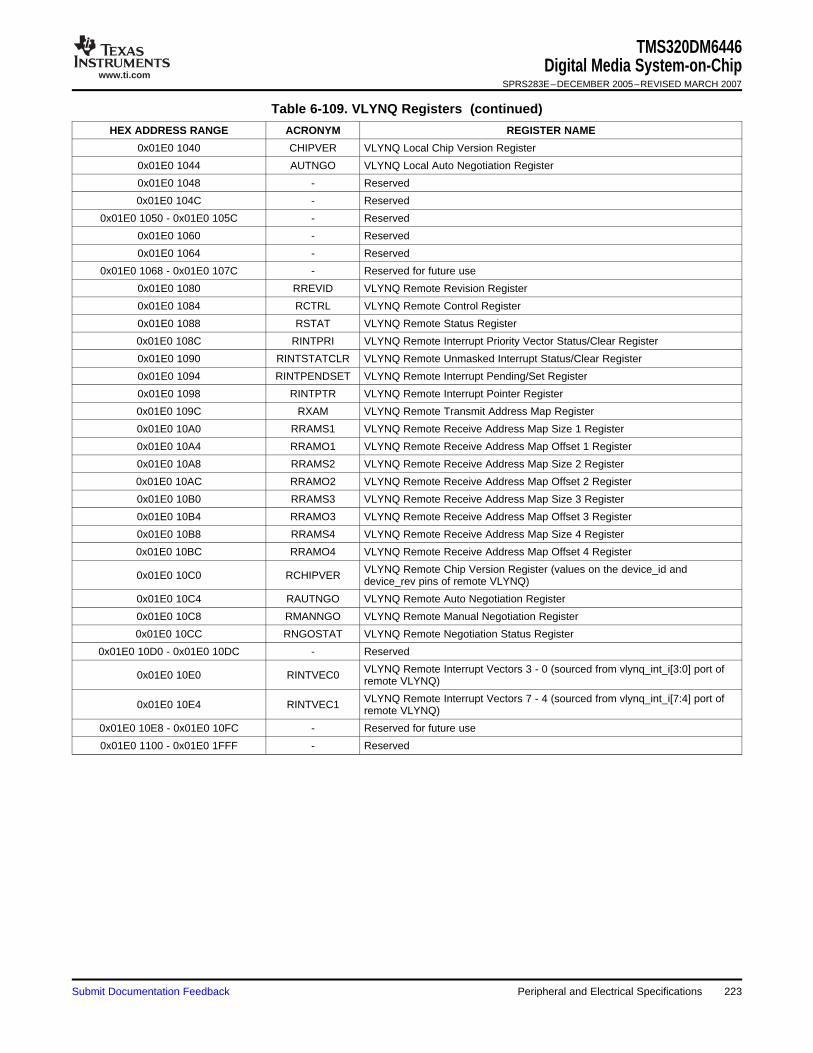
www.ti.com
TMS320DM6446Digital Media System-on-Chip
SPRS283E–DECEMBER 2005–REVISED MARCH 2007
Table 6-109. VLYNQ Registers (continued)
HEX ADDRESS RANGE ACRONYM REGISTER NAME
0x01E0 1040 CHIPVER VLYNQ Local Chip Version Register
0x01E0 1044 AUTNGO VLYNQ Local Auto Negotiation Register
0x01E0 1048 - Reserved
0x01E0 104C - Reserved
0x01E0 1050 - 0x01E0 105C - Reserved
0x01E0 1060 - Reserved
0x01E0 1064 - Reserved
0x01E0 1068 - 0x01E0 107C - Reserved for future use
0x01E0 1080 RREVID VLYNQ Remote Revision Register
0x01E0 1084 RCTRL VLYNQ Remote Control Register
0x01E0 1088 RSTAT VLYNQ Remote Status Register
0x01E0 108C RINTPRI VLYNQ Remote Interrupt Priority Vector Status/Clear Register
0x01E0 1090 RINTSTATCLR VLYNQ Remote Unmasked Interrupt Status/Clear Register
0x01E0 1094 RINTPENDSET VLYNQ Remote Interrupt Pending/Set Register
0x01E0 1098 RINTPTR VLYNQ Remote Interrupt Pointer Register
0x01E0 109C RXAM VLYNQ Remote Transmit Address Map Register
0x01E0 10A0 RRAMS1 VLYNQ Remote Receive Address Map Size 1 Register
0x01E0 10A4 RRAMO1 VLYNQ Remote Receive Address Map Offset 1 Register
0x01E0 10A8 RRAMS2 VLYNQ Remote Receive Address Map Size 2 Register
0x01E0 10AC RRAMO2 VLYNQ Remote Receive Address Map Offset 2 Register
0x01E0 10B0 RRAMS3 VLYNQ Remote Receive Address Map Size 3 Register
0x01E0 10B4 RRAMO3 VLYNQ Remote Receive Address Map Offset 3 Register
0x01E0 10B8 RRAMS4 VLYNQ Remote Receive Address Map Size 4 Register
0x01E0 10BC RRAMO4 VLYNQ Remote Receive Address Map Offset 4 Register
VLYNQ Remote Chip Version Register (values on the device_id and0x01E0 10C0 RCHIPVER device_rev pins of remote VLYNQ)
0x01E0 10C4 RAUTNGO VLYNQ Remote Auto Negotiation Register
0x01E0 10C8 RMANNGO VLYNQ Remote Manual Negotiation Register
0x01E0 10CC RNGOSTAT VLYNQ Remote Negotiation Status Register
0x01E0 10D0 - 0x01E0 10DC - Reserved
VLYNQ Remote Interrupt Vectors 3 - 0 (sourced from vlynq_int_i[3:0] port of0x01E0 10E0 RINTVEC0 remote VLYNQ)
VLYNQ Remote Interrupt Vectors 7 - 4 (sourced from vlynq_int_i[7:4] port of0x01E0 10E4 RINTVEC1 remote VLYNQ)
0x01E0 10E8 - 0x01E0 10FC - Reserved for future use
0x01E0 1100 - 0x01E0 1FFF - Reserved
Submit Documentation Feedback Peripheral and Electrical Specifications 223

www.ti.com
6.24.2 VLYNQ Electrical Data/Timing
VLYNQ_CLK
4
43
12
TMS320DM6446Digital Media System-on-ChipSPRS283E–DECEMBER 2005–REVISED MARCH 2007
Table 6-110. Timing Requirements for VLYNQ_CLK for VLYNQ (see Figure 6-76)
-594NO. UNIT
MIN MAX
1 tc(VCLK) Cycle time, VLYNQ_CLK 10 ns
Pulse duration, VLYNQ_CLK high [CLK External] 3 ns2 tw(VCLKH)
Pulse duration, VLYNQ_CLK high [CLK Internal] 4 ns
Pulse duration, VLYNQ_CLK low [CLK External] 3 ns3 tw(VCLKL)
Pulse duration, VLYNQ_CLK low [CLK Internal] 4 ns
4 tt(VCLK) Transition time, VLYNQ_CLK 3 ns
Figure 6-76. VLYNQ_CLK Timing for VLYNQ
Peripheral and Electrical Specifications224 Submit Documentation Feedback

www.ti.com
VLYNQ_CLK
VLYNQ_TXD[3:0]
VLYNQ_RXD[3:0]
1
2
3 4
Data
Data
TMS320DM6446Digital Media System-on-Chip
SPRS283E–DECEMBER 2005–REVISED MARCH 2007
Table 6-111. Switching Characteristics Over Recommended Operating Conditions for Transmit Data forthe VLYNQ Module (see Figure 6-77)
-594NO. PARAMETER UNIT
MIN MAX
Delay time, VLYNQ_CLK high to VLYNQ_TXD[3:0] invalid [SLOW Mode] 1 nstd(VCLKH-1TXDI) Delay time, VLYNQ_CLK high to VLYNQ_ TXD[3:0] invalid [FAST Mode] 0.5 ns
td(VCLKH-2 Delay time, VLYNQ_CLK to VLYNQ_TXD[3:0] valid 9.75 nsTXDV)
Table 6-112. Timing Requirements for Receive Data for the VLYNQ Module (see Figure 6-77)
-594NO. UNIT
MIN MAX
RTM disabled, RTM sample = 3 0.8 ns
RTM enabled, RXD Flop = 0 2.2 ns
RTM enabled, RXD Flop = 1 1.9 ns
RTM enabled, RXD Flop = 2 1.4 nsSetup time, VLYNQ_RXD[3:0] valid before3 tsu(RXDV-VCLKH) RTM enabled, RXD Flop = 3 0.8 nsVLYNQ_CLK high
RTM enabled, RXD Flop = 4 0.4 ns
RTM enabled, RXD Flop = 5 0.1 ns
RTM enabled, RXD Flop = 6 -0.2 ns
RTM enabled, RXD Flop = 7 -0.4 ns
RTM disabled, RTM sample = 3 2 ns
RTM enabled, RXD Flop = 0 0.6 ns
RTM enabled, RXD Flop = 1 1.0 ns
RTM enabled, RXD Flop = 2 1.5 nsHold time, VLYNQ_RXD[3:0] valid after4 th(VCLKH-RXDV) RTM enabled, RXD Flop = 3 2.0 nsVLYNQ_CLK high
RTM enabled, RXD Flop = 4 2.5 ns
RTM enabled, RXD Flop = 5 3.0 ns
RTM enabled, RXD Flop = 6 3.5 ns
RTM enabled, RXD Flop = 7 4.0 ns
Figure 6-77. VLYNQ Transmit/Receive Timing
Submit Documentation Feedback Peripheral and Electrical Specifications 225

www.ti.com
6.25 IEEE 1149.1 JTAG
6.25.1 JTAG Peripheral Register Description(s) – JTAG ID Register
TMS320DM6446Digital Media System-on-ChipSPRS283E–DECEMBER 2005–REVISED MARCH 2007
The JTAG (1) interface is used for BSDL testing and emulation of the DM6446 device.
The DM6446 device requires that both TRST and RESET be asserted upon power up to be properlyinitialized. While RESET initializes the device, TRST initializes the device's emulation logic. Both resetsare required for proper operation.
While both TRST and RESET need to be asserted upon power up, only RESET needs to be released forthe device to boot properly. TRST may be asserted indefinitely for normal operation, keeping the JTAGport interface and device's emulation logic in the reset state.
TRST only needs to be released when it is necessary to use a JTAG controller to debug the device orexercise the device's boundary scan functionality. Note: TRST is synchronous and must be clocked byTCK; otherwise, the boundary scan logic may not respond as expected after TRST is asserted.
RESET must be released only in order for boundary-scan JTAG to read the variant field of IDCODEcorrectly. Other boundary-scan instructions work correctly independent of current state of RESET.
For maximum reliability, DM6446 includes an internal pulldown (IPD) on the TRST pin to ensure thatTRST will always be asserted upon power up and the device's internal emulation logic will always beproperly initialized.
JTAG controllers from Texas Instruments actively drive TRST high. However, some third-party JTAGcontrollers may not drive TRST high but expect the use of a pullup resistor on TRST.
When using this type of JTAG controller, assert TRST to initialize the device after powerup and externallydrive TRST high before attempting any emulation or boundary scan operations.
(1) IEEE Standard 1149.1-1990 Standard-Test-Access Port and Boundary Scan Architecture.
Table 6-113. JTAG ID Register
HEX ADDRESS RANGE ACRONYM REGISTER NAME COMMENTS
Read-only. Provides 32-bit0x01C4 0028 JTAGID JTAG Identification Register JTAG ID of the device.
The JTAG ID register is a read-only register that identifies to the customer the JTAG/Device ID. For theDM6446 device, the JTAG ID register resides at address location 0x01C4 0028. The register hex value forDM6446 is: 0x0B70 002F. For the actual register bit names and their associated bit field descriptions, seeFigure 6-78 and Table 6-114.
31-28 27-12 11-1 0
VARIANT (4-Bit) PART NUMBER (16-Bit) MANUFACTURER (11-Bit) LSB
R-0000 R-1011 0111 0000 0000 R-0000 0010 111 R-1
LEGEND: R = Read, W = Write, n = value at reset
Figure 6-78. JTAG ID Register Description - DM6446 Register Value - 0xXB70 002F
Peripheral and Electrical Specifications226 Submit Documentation Feedback

www.ti.com
6.25.2 JTAG Test-Port Electrical Data/Timing
TCK
TDO
TDI/TMS
1
7
23
RTCK
4
56
9
8
TMS320DM6446Digital Media System-on-Chip
SPRS283E–DECEMBER 2005–REVISED MARCH 2007
Table 6-114. JTAG ID Register Selection Bit Descriptions
BIT NAME DESCRIPTION
31:28 VARIANT Variant (4-Bit) value. DM6446 value: 0000.
27:12 PART NUMBER Part Number (16-Bit) value. DM6446 value: 1011 0111 0000 0000.
11-1 MANUFACTURER Manufacturer (11-Bit) value. DM6446 value: 0000 0010 111.
0 LSB LSB. This bit is read as a "1" for DM6446.
Table 6-115. Timing Requirements for JTAG Test Port (see Figure 6-79)
-594NO. UNIT
MIN MAX
1 tc(TCK) Cycle time, TCK 20 ns
2 tw(TCKH) Pulse duration, TCK high 8 ns
3 tw(TCKL) Pulse duration, TCK low 8 ns
4 tc(RTCK) Cycle time, RTCK 20 ns
5 tw(RTCKH) Pulse duration, RTCK high 10 ns
6 tw(RTCKL) Pulse duration, RTCK low 10 ns
7 tsu(TDIV-RTCKH) Setup time, TDI/TMS valid before RTCK high 10 ns
8 th(RTCKH-TDIV) Hold time, TDI/TMS valid after RTCK high 1 ns
Table 6-116. Switching Characteristics Over Recommended Operating Conditions for JTAG Test Port(see Figure 6-79)
-594NO. PARAMETER UNIT
MIN MAX
9 td(RTCKL-TDOV) Delay time, RTCK low to TDO valid 15 ns
Figure 6-79. JTAG Test-Port Timing
Submit Documentation Feedback Peripheral and Electrical Specifications 227

www.ti.com
7 Mechanical Packaging and Orderable Information
7.1 Thermal Data for ZWT
7.1.1 Packaging Information
TMS320DM6446Digital Media System-on-ChipSPRS283E–DECEMBER 2005–REVISED MARCH 2007
The following table(s) show the thermal resistance characteristics for the PBGA–ZWT mechanicalpackage.
Table 7-1. Thermal Resistance Characteristics (PBGA Package) [ZWT]
NO. °C/W (1) AIR FLOW (m/s) (2)
1 RΘJC Junction-to-case 6.54 N/A
2 RΘJB Junction-to-board 15.62 N/A
3 29.75 0.00
4 26.78 1.0RΘJA Junction-to-free air
5 26.20 2.00
6 25.80 3.00
7 0.11 0.00
8 0.15 1.0PsiJT Junction-to-package top
9 0.16 2.00
10 0.16 3.00
11 14.79 0.00
12 14.66 1.0PsiJB Junction-to-board
13 14.66 2.00
14 14.66 3.00
(1) These measurements were conducted in a JEDEC defined 1S2P system and will change based on environment as well as application.For more information, see these EIA/JEDEC standards – EIA/JESD51-2, Integrated Circuits Thermal Test Method EnvironmentConditions - Natural Convection (Still Air) and JESD51-7, High Effective Thermal Conductivity Test Board for Leaded Surface MountPackages.
(2) m/s = meters per second
The following packaging information and addendum reflect the most current data available for thedesignated device(s). This data is subject to change without notice and without revision of this document.
Mechanical Packaging and Orderable Information228 Submit Documentation Feedback

PACKAGING INFORMATION
Orderable Device Status (1) PackageType
PackageDrawing
Pins PackageQty
Eco Plan (2) Lead/Ball Finish MSL Peak Temp (3)
TMS320DM6446ZWT ACTIVE BGA ZWT 361 90 Pb-Free(RoHS)
SNAGCU Level-3-260C-168 HR
TMS320VER6446ZWT ACTIVE BGA ZWT 361 Pb-Free(RoHS)
SNAGCU Level-3-260C-168 HR
TMX320DM6446ZWT ACTIVE BGA ZWT 361 TBD Call TI Call TI
(1) The marketing status values are defined as follows:ACTIVE: Product device recommended for new designs.LIFEBUY: TI has announced that the device will be discontinued, and a lifetime-buy period is in effect.NRND: Not recommended for new designs. Device is in production to support existing customers, but TI does not recommend using this part ina new design.PREVIEW: Device has been announced but is not in production. Samples may or may not be available.OBSOLETE: TI has discontinued the production of the device.
(2) Eco Plan - The planned eco-friendly classification: Pb-Free (RoHS), Pb-Free (RoHS Exempt), or Green (RoHS & no Sb/Br) - please checkhttp://www.ti.com/productcontent for the latest availability information and additional product content details.TBD: The Pb-Free/Green conversion plan has not been defined.Pb-Free (RoHS): TI's terms "Lead-Free" or "Pb-Free" mean semiconductor products that are compatible with the current RoHS requirementsfor all 6 substances, including the requirement that lead not exceed 0.1% by weight in homogeneous materials. Where designed to be solderedat high temperatures, TI Pb-Free products are suitable for use in specified lead-free processes.Pb-Free (RoHS Exempt): This component has a RoHS exemption for either 1) lead-based flip-chip solder bumps used between the die andpackage, or 2) lead-based die adhesive used between the die and leadframe. The component is otherwise considered Pb-Free (RoHScompatible) as defined above.Green (RoHS & no Sb/Br): TI defines "Green" to mean Pb-Free (RoHS compatible), and free of Bromine (Br) and Antimony (Sb) based flameretardants (Br or Sb do not exceed 0.1% by weight in homogeneous material)
(3) MSL, Peak Temp. -- The Moisture Sensitivity Level rating according to the JEDEC industry standard classifications, and peak soldertemperature.
Important Information and Disclaimer:The information provided on this page represents TI's knowledge and belief as of the date that it isprovided. TI bases its knowledge and belief on information provided by third parties, and makes no representation or warranty as to theaccuracy of such information. Efforts are underway to better integrate information from third parties. TI has taken and continues to takereasonable steps to provide representative and accurate information but may not have conducted destructive testing or chemical analysis onincoming materials and chemicals. TI and TI suppliers consider certain information to be proprietary, and thus CAS numbers and other limitedinformation may not be available for release.
In no event shall TI's liability arising out of such information exceed the total purchase price of the TI part(s) at issue in this document sold by TIto Customer on an annual basis.
PACKAGE OPTION ADDENDUM
www.ti.com 17-May-2007
Addendum-Page 1


IMPORTANT NOTICE
Texas Instruments Incorporated and its subsidiaries (TI) reserve the right to make corrections, modifications, enhancements,improvements, and other changes to its products and services at any time and to discontinue any product or service without notice.Customers should obtain the latest relevant information before placing orders and should verify that such information is current andcomplete. All products are sold subject to TI’s terms and conditions of sale supplied at the time of order acknowledgment.
TI warrants performance of its hardware products to the specifications applicable at the time of sale in accordance with TI’sstandard warranty. Testing and other quality control techniques are used to the extent TI deems necessary to support thiswarranty. Except where mandated by government requirements, testing of all parameters of each product is not necessarilyperformed.
TI assumes no liability for applications assistance or customer product design. Customers are responsible for their products andapplications using TI components. To minimize the risks associated with customer products and applications, customers shouldprovide adequate design and operating safeguards.
TI does not warrant or represent that any license, either express or implied, is granted under any TI patent right, copyright, maskwork right, or other TI intellectual property right relating to any combination, machine, or process in which TI products or servicesare used. Information published by TI regarding third-party products or services does not constitute a license from TI to use suchproducts or services or a warranty or endorsement thereof. Use of such information may require a license from a third party underthe patents or other intellectual property of the third party, or a license from TI under the patents or other intellectual property of TI.
Reproduction of information in TI data books or data sheets is permissible only if reproduction is without alteration and isaccompanied by all associated warranties, conditions, limitations, and notices. Reproduction of this information with alteration is anunfair and deceptive business practice. TI is not responsible or liable for such altered documentation.
Resale of TI products or services with statements different from or beyond the parameters stated by TI for that product or servicevoids all express and any implied warranties for the associated TI product or service and is an unfair and deceptive businesspractice. TI is not responsible or liable for any such statements.
TI products are not authorized for use in safety-critical applications (such as life support) where a failure of the TI product wouldreasonably be expected to cause severe personal injury or death, unless officers of the parties have executed an agreementspecifically governing such use. Buyers represent that they have all necessary expertise in the safety and regulatory ramificationsof their applications, and acknowledge and agree that they are solely responsible for all legal, regulatory and safety-relatedrequirements concerning their products and any use of TI products in such safety-critical applications, notwithstanding anyapplications-related information or support that may be provided by TI. Further, Buyers must fully indemnify TI and itsrepresentatives against any damages arising out of the use of TI products in such safety-critical applications.
TI products are neither designed nor intended for use in military/aerospace applications or environments unless the TI products arespecifically designated by TI as military-grade or "enhanced plastic." Only products designated by TI as military-grade meet militaryspecifications. Buyers acknowledge and agree that any such use of TI products which TI has not designated as military-grade issolely at the Buyer's risk, and that they are solely responsible for compliance with all legal and regulatory requirements inconnection with such use.
TI products are neither designed nor intended for use in automotive applications or environments unless the specific TI productsare designated by TI as compliant with ISO/TS 16949 requirements. Buyers acknowledge and agree that, if they use anynon-designated products in automotive applications, TI will not be responsible for any failure to meet such requirements.
Following are URLs where you can obtain information on other Texas Instruments products and application solutions:
Products Applications
Amplifiers amplifier.ti.com Audio www.ti.com/audio
Data Converters dataconverter.ti.com Automotive www.ti.com/automotive
DSP dsp.ti.com Broadband www.ti.com/broadband
Interface interface.ti.com Digital Control www.ti.com/digitalcontrol
Logic logic.ti.com Military www.ti.com/military
Power Mgmt power.ti.com Optical Networking www.ti.com/opticalnetwork
Microcontrollers microcontroller.ti.com Security www.ti.com/security
RFID www.ti-rfid.com Telephony www.ti.com/telephony
Low Power www.ti.com/lpw Video & Imaging www.ti.com/videoWireless
Wireless www.ti.com/wireless
Mailing Address: Texas Instruments, Post Office Box 655303, Dallas, Texas 75265Copyright © 2007, Texas Instruments Incorporated