Embed Size (px)
DESCRIPTION
Citation preview
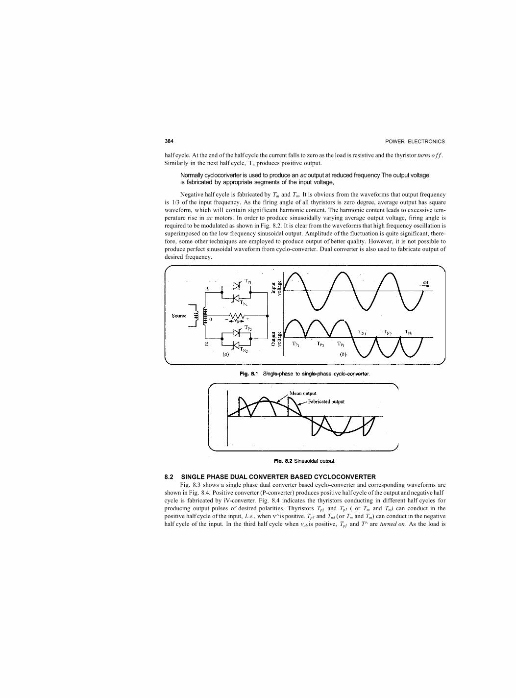
384 POWER ELECTRONICS
half cycle. At the end of the half cycle the current falls to zero as the load is resistive and the thyristor turns o f f . Similarly in the next half cycle, Tn produces positive output.
Normally cyclocoriverter is used to produce an ac output at reduced frequency The output voltage is fabricated by appropriate segments of the input voltage,
Negative half cycle is fabricated by Tm and Tm. It is obvious from the waveforms that output frequency is 1/3 of the input frequency. As the firing angle of all thyristors is zero degree, average output has square waveform, which will contain significant harmonic content. The harmonic content leads to excessive tem-perature rise in ac motors. In order to produce sinusoidally varying average output voltage, firing angle is required to be modulated as shown in Fig. 8.2. It is clear from the waveforms that high frequency oscillation is superimposed on the low frequency sinusoidal output. Amplitude of the fluctuation is quite significant, there-fore, some other techniques are employed to produce output of better quality. However, it is not possible to produce perfect sinusoidal waveform from cyclo-converter. Dual converter is also used to fabricate output of desired frequency.
8.2 SINGLE PHASE DUAL CONVERTER BASED CYCLOCONVERTER Fig. 8.3 shows a single phase dual converter based cyclo-converter and corresponding waveforms are
shown in Fig. 8.4. Positive converter (P-converter) produces positive half cycle of the output and negative half cycle is fabricated by iV-converter. Fig. 8.4 indicates the thyristors conducting in different half cycles for producing output pulses of desired polarities. Thyristors Tp} and Tp2 ( or Tm and Tm) can conduct in the positive half cycle of the input, L e., when v^is positive. Tp3 and Tp4 (or Tm and Tm) can conduct in the negative half cycle of the input. In the third half cycle when vab is positive, Tp] and T^ are turned on. As the load is

CYCLOCONVERTERS 385
resistive the current falls to zero at the end of this half cycle, consequently, both the thyristors are turned o f f . In the following half cycle Tm and Tm are turned on. As Tpi and Tn are already off there is no possibility of short circuit between two converters.
— _ — , — — — — — - — . — - — — — — — — - — . — — —
;>^Posit ive converter (P-converter) produces positive haIf cycle of the output and negative half cycle is fabricated by N~converter
If the output is not an integer submultiple then short circuit may take place. Let us take the case when T N\ and TN2 fired in the third half cycle, it is evident from the circuit that short circuit will take place as Tp{ and T^ are already conducting. Some amount of short circuit current is permitted to circulate between two convert-ers, therefore, in a particular scheme an intergroup reactor is placed between P and N converters to limit the circulating current.
P-converter N-converter
T p i z x i T P 3 TN2 AN4 V V
• <1 e
Tp4 7 \ A i p t ± i b
ANi
Fig. 8.3. Bridge type cyclo-converter
Fig. 8.4. Waveforms of bridge-type cyclo-converter.
8.3. CYCLOCONVERTER WITH INDUCTIVE LOAD In case of resistive load, current is in phase with the voltage, but with the inductive load the current lags
the voltage by an angle, </>(< 90°). Operation of the cyclo-converter can be explained with the help of the waveforms shown in Fig. 8.5.
In case of resistive load, current is in phase with the voltage, but with the inductive load the rrent lags the voltage by an angle, <j> ( < 90°).

386 POWER ELECTRONICS
From ty to tT P-converter operates in the rectification mode. At t7, load voltage changes its polarity but the current is still positive due to load inductance. After t2 negative voltage is produced by P-converter by controlling its firing angle between 90° and 180°. From t2 to t3 energy stored in the load inductance is fedback _ _ _ _ . _ _ _ . _
v _ y Fig. 8.5. Waveforms with inductive load.
to the source as the polarities of the voltage and the current are opposite. The converter in that duration operates as line commutated inverter. Similar operation takes place in the N-converter during the negative half cycle of the load current. Detailed explanation of the operation can be given with the help of the waveforms shown in Fig 8.6. In order to obtain sinusoidally varying average output voltage, firing angle is gradually varied. At point, A, appropriate thyristors are fired without delay to produce maximum mean voltage. At point, B, average value is slightly reduced by introducing some delay in the firing angle. At point C firing angle is further increased to reduce the average voltage. At tv firing angle is 90° for zero output voltage. From t2 to t3 P-converter is operated in inversion mode and firing angle is gradually increased to get higher negative average voltage. At tv load current falls to zero and the conducting thyristors, Tpl and Tpv turn off naturally. After some delay Tm and Tm are turned on. The delay is intentionally introduced to avoid any short circuit between two converters. It can be seen from the circuit that in this particular case, short circuit can not occur. Let us take the case when the load current falls to zero in the previous half cycle. At that point Tpl and Tn are under turn off process and and Tjv2 are turned on without any delay. It is clear from the circuit that short circuit will take place between two converters. Therefore, a delay is introduced in the firing signal of the incoming converter. In addition, intergroup blanking is used to block the operation of one of the converters. P and N converters are operated alternately. As circulating current is eliminated, the circuit is called non-circulating current cycloconverter. Control circuit of non-circulating cycloconverter is complex. In another scheme cycloconverter operates with a circulating current between two converters, however, the current is restricted by an intergroup reactor. The control circuit of this cycloconverter is comparatively simpler and the load voltage waveform is better compared to that of other scheme. At the same time, load current waveform is further improved by the filtering effect of the reactor. But, losses in the converters are increased by the circulating current. The reactor reduces the amplitude of the high frequency pulsation superimposed on the low frequency sinusoidal output. Due to the reduction of total harmonic distortion, performance of the motor type load is improved.

CYCLOCONVERTERS 387
°0 (Load voltage)
i (Load current)
Fabricated load voltage /
Input voltage
- Delay
Fig. 8.6 Waveforms of single-phase cyclo-converter.
Any type of cyclo-converter has inherent capability of power flow in either direction, so the circuit can deliver power at any power factor. Single phase to single phase cycloconverter is rarely used in practice. Three phase to single phase cycloconverter fabricates better waveform, because more pulses are available for fabricating output waveform.
type of cyclo-converter has inherent capability of power flow in either direction, so the circuit can deliver power at any power factor.
8.4. THREE PHASE TO ONE PHASE CYCLOCONVERTER As already mentioned that single phase to single phase cycloconverter is rarely used. Before explaining
the operation of the circuit let us develop the expression for output voltage. Fig. 8.7 shows a three phase,
c
B
A
j B \ 7 1 c 1
Load
Output voltage
N
Fig. 8.7. Three-pulse converter.

338 POWER ELECTRONICS
three pulse P-converter and its output waveforms for constant firing angle. Time origin is taken at the instant of the peak value of vA. Thyristor, JA, is fired at - 71/3 + a.
Average voltage is given by 1 fin/3+a I
v* = wUJ2VphC0S<0td(0t
Where VDh c o s 0)1 is the equation of phase voltage, vA. From above,
V, = V2 V, ph
= Vdocosa
sm cos a
Where vdo •̂ ifHf For converter of m phases , V, is given by
V ^ V I v J f W * m
If V0 is the rms value of the fundamental component of the output then,
V2Vn = yf2V„ii - I sinl - I cos a
or v0=vph
p\n)~"\3)~ 3) . ( k ) sin — cosa
...(8.1)
...(8.2)
...(8.3)
...(8.4)
...(8.5)
. n j 1 3 , - ( 8 - 6 )
From eqn. 8.3, graphical relation between average voltage and angle is plotted, which is shown in Fig. 8.8.
-rectification
Fig. 8.8 Modes of operation of converters.
Curve 1 is for P-converter and curve 2 is for iV-converter (Fig.8.9) It is clear from the curve 1 that for 0° < a < 90°, P-converter operates as a rectifier and for 90° < a < 180°, the converter operates as an inverter.

CYCLOCONVERTERS 389
Rectification and inversion properties are utilised in cyclo-converter to produce ac output when inductive load is connected to it. By suitably controlling the firing angle, average output can be varied sinusoidally. Fig. 8.9 shows a six thyristor, three pulse cycloconverter. An interphase reactor can be omitted if non-circulating current scheme is adopted.
r m 2 i i S Z \ A
P-converter q f W T W W
N-converter
Intergroup reactor Load
N •
Fig. 8.9. Three-pulse mid-point cyclo-converter.
8.4.1. Cycloconverter with R-Load For simpler explanation iMoad is considered. As energy feedback is not required, inversion mode of the
converters is redundant. Fig. 8.10 (a) shows the waveforms for P-converter during positive half cycle of the output. As seen from the waveforms, at point A appropriate thyristor is fired without any delay and maximum average voltage is obtained. At B some delay is introduced to decrease the average voltage. At C firing angle is further delayed for further reduction of the voltage. Thus a sinusoidally varying positive half cycle of the output is produced. In the similar manner negative converter operates during negative half cycle, as shown in Fig. 8.10(b).
8.4.2. Cycloconverters with R-L Load When the cycloconverter operates with R-L load, both rectification and inversion modes are used. In the
rectification mode a is varied from 0° to 90° and in inversion mode a is between 90° and 180°. Fig. 8.11 (a) shows the waveforms of P-converter in the rectification mode. It is clear from the waveforms that for peak value of the mean output, firing angle is minimum and it is increased on either side. Fig. 8.11.(b) shows the output of P-converter operating in inversion mode. It can be seen that a is varied between 90° and 180°. At point A' firing is with maximum delay which gives maximum negative voltage. At point B' the angle is slightly decreased to reduce the average voltage. Fig. 8.11(c) illustrates the output of N-converter for rectification mode. Fig 8.12 shows the waveforms corresponding to the complete cycle of output. It is seen that at t3 a delay is introduced.
hen the cycloconverter operates with R-L load used.
both rectification and inversion modes are


CYCLOCONVERTERS 391
V J
Fig. 8.11. Waveforms of P and N converters for R-L load.
8.5. BRIDGETYPECYCLOCONVERTER It comprises 12 thyristors for producing single phase output. Basically it is a dual converter operated in
a particular manner to produce sinusoidal output. Fig. 8.13 shows the circuit.
8.5.1. Output with R-Load As seen earlier, bridge converter produces six pulse output. Average value of the output is given by
m in this case is 6 As seen earlier, converters of this circuit can operate as rectifier or inverter. Fig. 8.14 (a) shows the
waveforms, when P-converter acts as a rectifier for ap = 30°. TV-converter is operated at aN = 150° (Fig. 8.14 (b)). Average voltages produced by both converters are same but their instantaneous voltages are quite different, which will result in circulating current. Intergroup reactor limits the current circulating between two converters. Reactance offered by one half is X. If both the halves are perfectly coupled then total reactance offered to the circulating current is 4X. In this case instantaneous value of the load voltage is the average of the instanta-neous values of the output voltages of P and TV converters. Load voltage waveform is shown in fig. 8.14 (c) for the condition ap + o^ = 180°.
8.5.2. Non-Circulating Current Seheme Circulating current can be avoided by intergroup blanking, i.e. when one converter is operating, firing pulses
to other converter are blocked. In addition to this, a delay is introduced for incoming converter at the time of change over. Fig. 8.15 (a) shows the waveforms with R-L load. As the number of pulses in this case is twice that of the output of three pulse converter, the load voltage waveform is better. The load voltage is varied sinusoi-dally by suitable variation of the firing angle. Filtering effect of the reactor also helps in reducing the harmonic content in the load current.
Circulating current can be avoided by intergroup blanking, i.e. when one converter is operating, firing pulses to other converter are blocked.
...(8.7)
where ...(8.8)

408 POWER ELECTRONICS
(3 can be calculated from the above transcendental equation by iterative method. (3 can also be determined as follows:
Eq. 9.22 can be written as
A graph is plotted between iQ and m (oof > 180°). When io becomes zero, then the corresponding value of (tit is equal to the extinction angle, (3. Thyristor, Tv conducts from a to (3.
The conduction angle, y, is given by y=(3-a.
If y < 180° then the load current is zero for some time. This is a case of discontinuous conduction. When a = § then each thyristor conducts for 180°. In this condition the circuit behaves as if R-L load is directly connected to ac source. If OC is further reduced then there will not be any effect on the working of the circuit. Let T2 be conducting and Tx is given gate pulse at a < Until Thyristor T2 stops conduction. Tx
cannot be turned on. T2 turns off at <|) then Tx is turned on. If Tx is given a narrow gate pulse then it will rail to turn on after T2 ceases to conduct, and the circuit behaves as a rectifier. In order to avoid this malfunc-tioning, continuous gate pulse or pulse train should be supplied as gate signal to both thyristors. Gate pulse should be supplied to T{ from a to 180°, similarly gate pulse to T2 must be supplied from 180°+a to 360°.
9.1.3. AC Regulator with Purely Inductive Fig. 9.6. shows the waveforms of regulator
with inductive load. When a = 90° the circuit behaves as if load is directly connected to ac source. Average power over a cycle is zero. For a > 90° current flows from a to 2n - a and from n + a to 37t - a . Current through Tx is symmetrical about 180° point. Average power supplied to the load by the thyristor T{ is zero as seen from the waveforms. This is in accordance with the fact that inductance does not consume any power. Fundamental component of the load current will lag the supply voltage by 90°. The value of the fundamental component can be controlled by the firing angle,
Vm a. And it can be varied from J ^ ^ to 0 by controlling firing angle from 90° to 180°. Thus reactance offered by the regulator can be varied from 0) L to infinity. So the regulator with inductance load behaves as a variable reactor.
Fundamental component of the toad current will lag the supply voltage by 90°.
This circuit is used in static reactive power compensators. (Refer to example 9.6)
Fig. 9.6 Waveforms of Regulator with Inductive Load.

A.C. REGULATOR 409
9.1.4. Working of other Regulators Working of other regulators will be considered only with R load. /
Fig. 9.7. Waveforms of regulators with R-load.
Triac, shown in the circuit of Fig. 9.1.1 (b), conducts from a to n and ft + a to 2n. Gate pulse to triac is provided in each half cycle. Same output is produced by the circuit of Fig 9.1 (c). In the positive half cycle current flows through Dv Tand D2 . In the negative half cycle load current flows through Dv Tand D4. Due to presence of the rectifier only one thyristor is required, which makes it cheaper compared to the regulator of two antiparallel thyristors. Electrical isolation between gate and control circuit is not necessary. Electrical isolation may be made redundant by the use of another configuration shown in Fig. 9.1 (d). In the positive, half cycle load current flows through T{ and D{ and in the negative half cycle load current flows through T2
and Dt
9.1.5. Synchronous Tap Changer Thyristors can be used as static switches for on-load tap changing of transformers. Static tap chang-
ers are very fast in operation. Fig. 9.8 shows a circuit with two taps. The circuit can also be used for improvement of line power factor. As a tap changer, regulators are required to conduct for full cycle in order to provfde sinusoidal voltage.
Thyristors can be used as static switches for on-load tap changing of transformers.
Tl
Si
kV
t 2
T3
k< 1
S2 T4
Load
Fig. 9.8. Synchronous tap changer.

410 POWER ELECTRONICS
When switch S} (T{ & T2) conduct for full cycle, output voltage is equal to V. If gate pulses to T{ and T2 are blocked, and T3 and T4 are turned on for full cycle conduction then reduced voltage, KV, appears across the load.
The circuit can be used to improve power factor. In an ac regulator, firing angle control is employed to control the output voltage. At low output voltages, firing angle is high. So, output voltage is significantly distorted resulting in higher percentage of harmonics. Both displacement factor and distortion factor will be low leading to low power factor. Synchronous tap changer can be employed to improve the performance. A comparison will be made between two cases. In one case only Sx is operated from 0 to 180°. In other case only S2 is operated. For simpler analysis, resistive load is considered and K = 0.5. Curve 1 is for output voltage and P. F. when switch, Sv is operated. For a < 90° p.f. is more than 0.707.
an ac regulator, firing angle control is employed to control the output voltage.
1.0
£ O.s P-t
0.6 W) 3 0.4
§ 0.2 O-
P.F. and output
Vvoltage
-J I 1 I I L i i i i i 71/2
Firing angle a Fig. 9.9. Variation of output voltage and P.f. with firing angle.
For a >90° there is a significant reduction in its value. At a =135°, power factor is intolerably low. Curve 2 is for the output voltage when switch S2 is operated. Its input power factor curve (3) is same as in other case. If we want to have V0= 0.4 then thyristor, 7y, of switch Sv is fired at about 125°. Input power factor is also 0.4. If switch S2 is operated instead of Sv then thyristor T3 of S2 is fired approximately at 75°. Corresponding input power factor is about 0.85. So we can conclude that if the output is obtained from lower tapping then due to reduced firing Fig. 9.10 Load voltage waveform for R-load
angle there is a considerable improvement in power factor. For output voltage VQ, in the range 0 to 0.5 P. £/., operation of S2 is desirable. For V0 > 0.5 P U, operation of the circuit is explained in next para.
In the positive half cycle thyristor, Tv is fired at 0°. At cot = a thyristor, Tv is turned on. T3 is reverse biased by the line voltage from upper tapping and it is turned o f f . Output voltage has two part. One part is obtained from lower tapping and other part from upper tapping. Fig. 9.10. Shows the Waveform.
If the output is obtained from lower tapping then due to reduced firing angle there is a considerable improvement in power factor.
R-Lioad Due to presence of inductance, current continues to flow in the next half cycle, therefore, load
voltage waveform will be different. Let Tx be fired at a in positive half cycle. Due to inductance of load, it will continue to conduct until cot = 6.

A.C. REGULATOR 411
Thyristor T4 cannot be triggered before m= p. At m = (3, thyristor T4 is turned on. At cot = n + a thyristor T2
is fired which turns off T4 due to line commutation. Load voltage waveform is shown in Fig. 9.11.
As seen from Fig. 9.11., rate of rise of current is less when thyristor T3
or T4 conducts and the rate is higher when thyristor Tx or T2 is on. This is due to higher load voltage when a thyristor from upper pair is conducting. Gate pulse to Tx should be applied from a to n and thyristor T2 must be given from n + a to 2n. A pulse train is the most suitable signal for firing.
There is a possibility of short circuit. This undesirable operation can take place when thyristors T{ and T4 are turned on simultaneously in positive half cycle. Voltage in upper section of secondary winding provides voltage for short circuit current. Similarly in negative half cycle thyristors T2 and T3 can provide a short circuit path. Therefore, adequate protection should be provided against such mal-operation.
Let us consider that switch, Sv is conducting for full cycle to provide KV output. In order to raise the level of the voltage, switch, Sv is also provided gate pulses. In the negative half cycle T4 is fired which continues to conduct until n +(3 (extinction angle in next positive half cycle). If the thyristor, Tv is fired in the next positive half cycle before T4 turns off then upper section of the winding is short circuited by T{ and r4. Similar operation may take place by simultaneous conduction of T2 and Ty
Fig. 9.11 Load voltage and current waveform for R-L load.
9.1.6. Multistage ac Regulator In place of two stage sequence control,
multistage sequence control can be used for further improvement of power factor and output voltage waveform. Fig 9.12 shows the circuit. It has n secondary sections each having VJn voltage. If the pair n- 4 is fired at a = 0° then output voltage is (n - 4)VJn. For the variation of voltage from (n - 4) VJn to (n - 3)VJn , firing angle of the pair (n - 3) is controlled from 180° to 0°. Thus the load voltage can be varied from 0 to Vs by selecting appropriate adjacent pairs. This circuit requires large number of pairs. An alternate circuit is shown in fig. 9.13 which requires less number of thyristors. It is cheaper compared to above mentioned circuit.
The circuit has (n + 1) stages i.e., 0, 1,2 n . If voltage of 0 stage is V then voltage of nth
section is 2n~l V. In the circuit shown in Fig. 9.13, n = 4.
"I 1 : 1 H>tr
n-1
Load
Fig. 9.12 Multistage sequence control.

416 POWER ELECTRONICS
9*3. OTHER APPLICATIONS Single phase and three phase ac regulators can be used as bus transfer switch, three phase sequence
changer* ac circuit breaker etc.
9.3.1. Bus Transfer Switch Fault at any bus results in the interruption of power flow to all connected loads. In order to maintain
the flow of power, the loads must be connected to some other bus. In substations, circuit breakers and isolators are used. Fig. 9.17 (a) shows a single phase bus transfer switch. In case of fault at bus 1, firing pulses to thyristors of Sx are blocked and thyristors of switch, S2, are turned on. The switch, S2, connects the load to bus 2. Fig. 9.17 (b) shows a three phase bus transfer switch
Fig. 9.17. Bus transfer switch.
9.3.2. Phase Sequence Changer Reversal of phase sequence is required in many applications, viz., reversal of rotation and electric
braking (by plugging) of three phase induction motor. Fig. 9.18 shows the circuit which provides fast and sparkless phase sequence reversal. Initially thyristors of SA, SB and Sc are fired for providing continuous connection between supply and load terminals. Load terminal a is connected to A. Similarly b is connected to B and c with C.
Reversal of phase sequence is required in many applications, viz., reversal of rotation and electric braking (by plugging) of three phase induction motor.

A.C. REGULATOR 417
Whenever phase sequence reversal is re-quired then thyristors of SB and Sc are turned off and thyristors of S'B and S'c are turned on. By turning on S'B and S'c, load terminals c and b are connected to B and C respectively, thus phase sequence of load is changed to ACB. The reversed phase sequence produces a rotating field (in the induction motor) in the opposite direction.
Reverse rotating field tends to rotate the motor in the reverse direction. If the motor is al-ready running then rotating field in opposite di-rection produces a braking torque, which quickly stops the motor and then rotates the motor in the opposite direction. This type of braking is called plugging, which requires large stator current be-cause the slip between rotor and flux is about 2. Braking current can be about 12 times the full load current. Therefore, thyristors of the circuit must have very large current rating. Fig. 9.18 Phase sequence Changer
Reverse rotating field tends to rotate the motor in the reverse direction. If the motor is already running then rotating field in opposite direction produces a braking torque, which quickly stops the motor and then rotates the motor in the opposite direction.
9.3.3. AC Circuit Breaker In usual ac regulator, thyristor
current falls to zero in other half cy-cle. In case of short circuit very large current flows through the conduct-ing thyristor. In order to protect the thyristor from over current, forced commutation may be employed. Fig. 9.19 shows ac circuit breaker. Capaci-tors, Cx and C2, are charged to peak value through D{ and D2 respectively. Let Tm{ be conducting and fault takes place. A current feed back circuit is used. On detection of over current, firing pulses are generated by con-trol circuit which turns on auxiliary thyristor T&v as a result, the charged capacitor, Cp turns offT x by forced voltage commutation. Similarly T 2
can be turned off by Ta2 and C2 Fig. 9.19. AC circuit breaker.
In order to protect the thyristor from over current, forced commutation may be employed.

Power Electronics & Electric Drives {EE/EEEJ 8 - 2 GATE ACADEMY PUBLICATIONS GATE ACADEMY PUBLICATION.'
L Introduction : AC voltage controllers are thyristor based device which convert fixed alternating voltage directly to variable alternating voltage without a change in the frequency. Some of the main application of ac voltage controllers are for domestic and industrial heating, transformer tap changing, lighting control, speed control of single-phase and three phase ac drives and starting of induction motors.
The main disadvantage of ac voltage controllers is the introduction of objectionable harmonics in the supply current and load voltage waveforms, particularly at reduced output voltage levels.
2* Single phase half-wave ac voltage controller
h>A H < H
Dl sin
+ v.l l i ? 4
xot
2tc '
Fig. Power-circuit diagram
Cff Average output voltage : 1 f2?r V V
VQ -— F sinwtdmt =— [cosa-cos(27i)] = — [cosot-1] 2 % J a 2iz 0 f r r
^(ij^Average output current I0 / Average input current:
V V 5 R 2kR j
(W) RMS output voltage
Fig. Voltage and current waveforms
1 2̂71
P-4K
2n-a + sin 2a V
iJn 271 - a +
sin 2a 2
/ V 1 s{pr)Power factor : 2n~a +
sin2a a
yTThe source current contains DC components and saturates the transformer core therefore half controlled // regulator not preferred for applications.
Sol . Given : R load, a = For single phase half PMMC reads average
3. Single-phase J 3 . 1 R l o a d :
V. L
Average oi
v^ir) RMS outpi
ower fact
• GATE A C A D E M Y PUBL ICAT IONS • GATE A C A D E M Y PUBL ICAT IONS • GATE A C A D E M Y PUBL ICAT IONS • GATE A C A D E M Y PUBL ICAT IONS • * GATE ACADEMY PUBLICATI
Copyrights © All rights reserved by GATE ACADEMY PUBLICATIONS. No part of this booklet may be reproduced or utilized in any form without the written permission. Copyrights © AH rights reserved by C

Electronics & Electric Drives [EE/EEE] 8 - 2 GATE ACADEMY PUBLICATIONS™
1 .
2.
Introduction : AC voltage controllers are thyristor based device which convert fixed alternating voltage directly to variable alternating voltage without a change in the frequency. Some of the main application of ac voltage controllers are for domestic and industrial heating, transformer tap changing, lighting control, speed control of single-phase and three phase ac drives and starting of induction motors. The main disadvantage of ac voltage controllers is the introduction of objectionable harmonics in the supply current and load voltage waveforms, particularly at reduced output voltage levels.
Single phase half-wave ac voltage controller :
H < H
© D1 F_ sin art
Fig. Power-circuit diagram 'A Average output voltage :
:R
1 f27t V v V0= — \ Vm sin© tdm = —[cos a - cos(2tt)] = -^-[cosoc-1]
2tc J a 2TC 2TT
Fig. Voltage and current waveforms
F
J i j^Averag< ;e output current I0 / Average input current:
V V I =— = — — [ c o s a - 1 ]
* R 2%R
(m) RMS output voltage
I 1 f27i 2 I 1 f2* 2 ( 1 - C O S 2 © 0
lv m 4%
2n-a + s i n 2 a PL
2 7 i - a + sin 2a
m )Power factor K 42
2n-a + sin 2a
a
he source current contains DC components and saturates the transformer core therefore half controlled regulator not preferred for applications.
^ Q P O l A C A D E M Y PUBLICATIONS • GATE A C A D E M Y PUBL ICAT IONS • GATE A C A D E M Y P U B L I C A T I O N S • GATE A C A D E M Y PUBL ICAT IONS •
- ^ ^ h t s © All rights reserved by GATE ACADEMY PUBLICATIONS. No part of this booklet may be reproduced or utilized in any form without the written permission.

GATE ACADEMY PUBLICATIONS ™ 8 - 3 AC Voltage Controllers & Cycloconverters
Example 1 A single phase half wave AC voltage controller feeds a R load for a firing angle of 180°PMMC voltage across the load would read.
Sol. Given :R load, a = 180° For single phase half wave controller, PMMC reads average voltage :
3.
V0 = — fV sinco/ = — F J c o s a - 1 ] = —Vm[-2] = -0 2 71 a M 271 271
K 71
Single-phase full-wave ac voltage controller : 3.1 E l o a d %
+ 1 0 F M s i
& T2 shunt :R
Fig. Power-circuit diagram
V / R fit
Fig. Voltage and current waveforms J& Average output voltage : V0 = 0
^ r ) RMS output voltage :Vor=. - f (Vm sin co tf = i 7 i - a + -sin 2 a
w-fm)Power factor : — = -4= K J%
n - a + -s i n 2 a
A n s .
• GATE A C A D E M Y P U B L I C A T I O N S • GATE A C A D E M Y PUBL ICAT IONS • GATE A C A D E M Y PUBL ICAT IONS • GATE A C A D E M Y PUBL ICAT IONS
Copyrights © All rights reserved by GATE ACADEMY PUBLICATIONS. No part of this booklet may be reproduced or utilized in any form without the written permission.
Power Electronics & Electric Drives [EE/EEE] 8 - 4 GATE ACADEMY PUBLICATIONS™
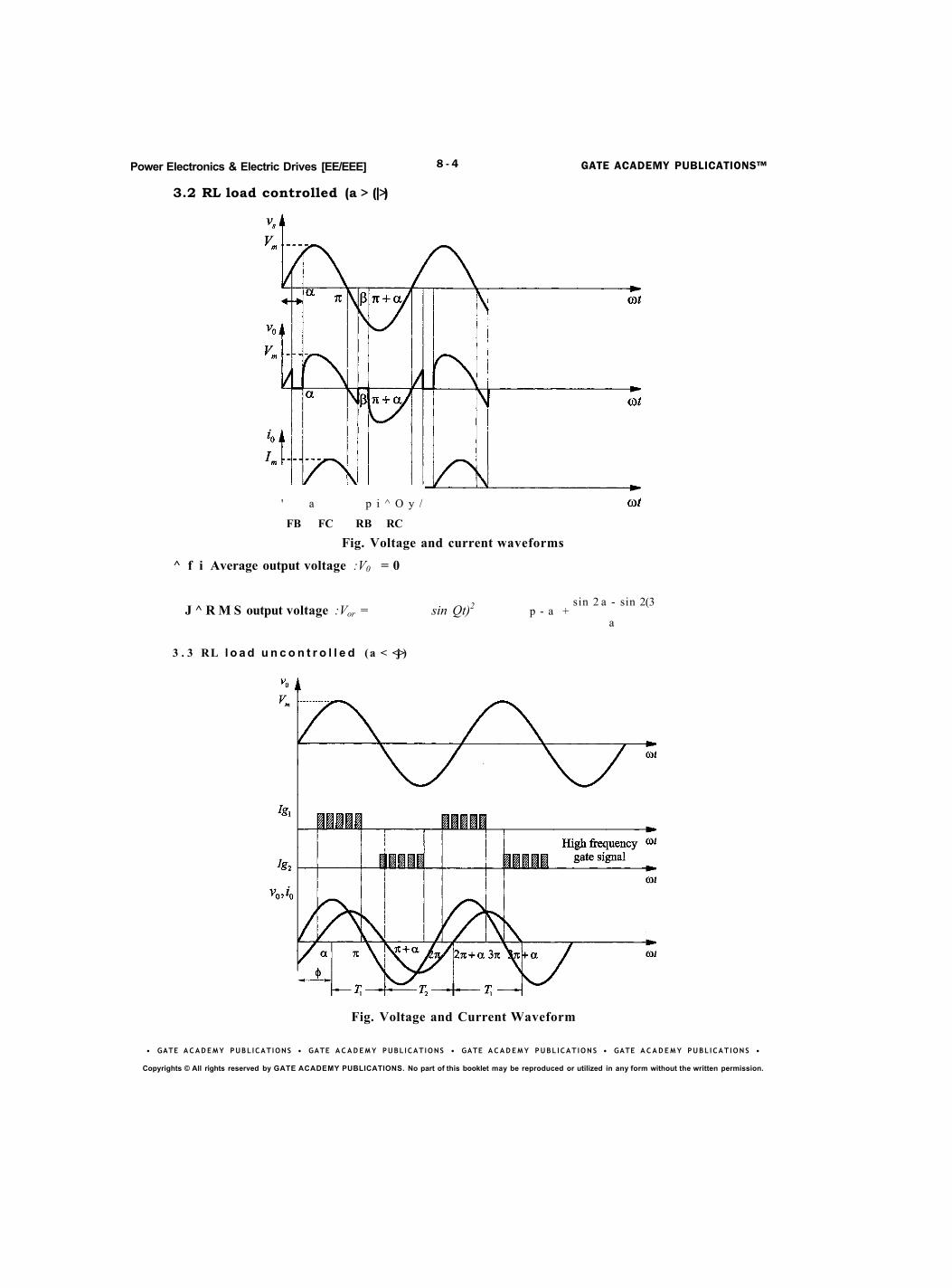
3.2 RL load controlled (a > (|>)
' a p i ^ O y /
FB FC RB RC
Fig. Voltage and current waveforms
^ f i Average output voltage :V0 = 0
J ^ R M S output voltage :Vor = sin Qt)2
3 . 3 RL l o a d u n c o n t r o l l e d (a < <j>)
p - a + sin 2 a - sin 2(3
a
Fig. Voltage and Current Waveform
• GATE A C A D E M Y PUBL ICAT IONS • GATE A C A D E M Y PUBL ICAT IONS • GATE A C A D E M Y P U B L I C A T I O N S • GATE A C A D E M Y PUBL ICAT IONS •
Copyrights © All rights reserved by GATE ACADEMY PUBLICATIONS. No part of this booklet may be reproduced or utilized in any form without the written permission.

GATE ACADEMY PUBLICATIONS ™ 8 - 5 AC Voltage Controllers & Cycloconverters
(i) Average output voltage : VQ = 0
(ii) RMS output voltage :Vor=Vs.
If pulse gate signal is given to ac voltage controller then it may behave as half wave rectifier because one of the SCR fails to turn on. To avoid this problem we must give high frequency gate pulse to thyristor.
S TRIAC cannot be used for inductive load with time constant.
4. 2 stage AC voltage controller :
• a
71J7
© |VS
V . I L :
i v s
L=
7 > K
1 Fig. Circuit diagram Fig. Voltage waveform
(i) RMS output voltage : Vor = £(Fm sincotf d®t + £ { I V m s in®tfd®t
42% a - 0 +
sin 2 x 0 - sin 2a /
+ 4 sin 2a
7 i - a + J V 2 j
_ vM
yjln
F
^ sin 2a . . . . . a - 0 + 471-4a+ 2 sin 2a
\fliz
(ii) RMS value of thyristor current
4 7 i - 3 a + 3 sin 2 a
|2tcH R
(iii)RMS value of thyristor current:
lJ%R a
sin 2a
4 / 4 J 1 rnf 2Vm sin co ̂
R
\2 dmt =
2 F
V4tzR 7 i - a + -
sin 2a J%R
7 i - a + -sin 2a
• GATE A C A D E M Y PUBL ICAT IONS • GATE A C A D E M Y PUBL ICAT IONS •> GATE A C A D E M Y PUBL ICAT IONS • GATE A C A D E M Y PUBL ICAT IONS •
Copyrights © All rights reserved by GATE ACADEMY PUBLICATIONS. No part of this booklet may be reproduced or utilized in any form without the written permission.

Power Electronics & Electric Drives [EE/EEE] 8 - 1 0 GATE ACADEMY PUBLICATIONS™
Mid-Point Type
. v,
Full-Bridge Type
Possible o/p Voltage
Fig. Voltage waveform of step up cycloconverter mmmmmmmmmmmmmmmmmmmmm 1) For low speed high power reversible operation the most suitable drives are cycloconverter based a.c
[rives Ex: Machine tool drive. li) Advantage of cycloconverter is load commutation is possible in step down chopper.
(iij^Quality of ac voltage of cycloconverter is improved with increase in output voltage at increased frequency because ripple decreases as frequency increases
(iv)18 Switches are used to construct a three phase cycloconverter. (v) An intergroup reactor is used in a single phase cycloconverter circuit to limit the circulating current.
l)Cycloconverter has poor power factor.
• • • •
• GATE A C A D E M Y PUBL ICAT IONS • GATE A C A D E M Y PUBL ICAT IONS • GATE A C A D E M Y PUBL ICAT IONS • GATE A C A D E M Y PUBL ICAT IONS *
Copyrights © All rights reserved by GATE ACADEMY PUBLICATIONS. No part of this booklet may be reproduced or utilized in any form without the written permission.

348 POWER ELECTRONICS
Q. 11. Explain operation of single phase full bridge inverter. Q.12. Discuss briefly about transistor and thyristor inverters.
[RGPV, June 2004] [RGPV, Dee. 2004]
Q.13. Discuss the domestic inverters. Explain the practical problems. Q. 14. Draw the load current wave form of R-L-C circuit or under damped R-L-C circuit. Q.15. Draw the output voltage wave form of 180° conduction scheme of three/phase inverter. Also draw
the turn on sequence table of thyristor. Q.16. What are the advantages of 120° conduction scheme of three phase inverter? Draw the turn on
sequence and draw the wave forms. Q.17. Discuss single phase auto sequential commutated inverter [ASCI]. Draw its equivalent circuit of
operation. Q.18. Describe DC side commutated inverter. Q.19. Why we need modified series inverter? Discuss the same. Q.20. Discuss Equal pulse width modulation [EPWM]. Q.21. How PWM control method is used three phase induction motor applications ? Explain. Q.22. Compare between series inverter and parallel inverter.

C H
Chopper INTRODUCTION
In industrial application it is required to convert a fixed voltage dc source into a variable dc source. DC chopper converts directly from dc to dc. A chopper can be considered as dc equivalent to ac T/F with a continously variable turns ratio. Like a T/F it can be used as step down or step up a dc voltage source.
Choppers are widely used for traction motor control in electronic automobiles, trolley cars, marine hoists. They provide smooth acceleration control, high efficiency and fast dynamic responce. Choppers can be used in regenerative breaking of dc motor to return energy back into the supply and this feature results in energy saving for transportation system with frequent stop. Chopper is also used in dc voltage regulators and also used with inductor to generate a dc current source.
D. C. chopper is a solid state circuit which provides a variable voltage dc output from a constant voltage dc source. It is used to control dc motor of electric automobile, trolley cars, forklift trucks, marine hoists, etc. It is also used for battery charging and it is essential in battery operated vehicles. As any other semiconductor circuit, chopper provides smooth and fast acceleration and efficient power control. There are two types of chopper : (1) step down chopper is used to reduce the output voltage. Its output voltage is less than the input voltage and (2) step up chopper is used to increase the voltage above input level.
7.1. STEP DOWN CHOPPER Chopper is basically a series switch, which is turned on and turned off at high frequency to get square
pulse train. Average voltage can be controlled by varying the ratio of turn on and turn off periods. Fig. 7.1. shows the basic circuit of step down chopper. Transistor, thyristor or GTO can be used as series switch. Usually load is inductive. Therefore, a freewheeling diode is connected across the load for circulation of load current when the transistor is turned o f f .
Chopper is basically a series switch, which is turned on and turned off at high frequency to get square pulse train.
At the beginning of on period, Ton, the transistor is turned on. During this period, load voltage, v0, is equal to Vs and the load current rises exponentially. When the transistor is turned o f f , the load current circulates through freewheeling diode, DFW. Because of conduction of freewheeling diode, the load voltage drops to zero. The energy stored in the load inductance is gradually dissipated in the load resistance, hence, load current decays exponentially.
i A F T E R 7

350 POWER ELECTRONICS
Fig. 7.1. Step down chopper and waveforms.
Average voltage is found as
1 TJO T
v0dt ...(7.1)
...(7.2)
= a K where r is the time period of chopping and a is the duty cycle which is equal to the time ratio Ton/T.
By controlling duty cycle, a, load voltage can be controlled from 0 to V. The load voltage can be less than or equal to the source voltage and the power flows from the dc source to the load. The chopper is called step down chopper. During on state inductorabsorbs the energy and during freewheeling period it releases the stored energy. Therefore, average energy (in the load inductance) per cycle is zero. Consequently average voltage across the inductor is also zero. If I{ and /2 are the average values of the input and load currents, then
...(7.3)
...(7.4) or Vsh^Voh
The relations expressed in above equations are equivalent to the relations of a transformer. Duty cycle, a, of the chopper corresponds to the turns ratio of a transformer. DC chopper can be considered as dc transformer whose turns ratio, a, can be varied by controlling the time ratio.
7.2. Step Up Chopper The basic circuit which can produce an output voltage greater than the source voltage is shown in
Fig. 7.2. At the beginning of the on period, transistor, T, is closed. The inductor current begins to rise linearly. The rate of rise of the current is equal to Vs/L.
tn step up chopper circuit which can produce an output voltage greater than the source voltage

CHOPPER 351
Fig. 7.2. Step up chopper.
The diode is used to prevent discharging of the capacitor through the conducting transistor. When the transistor is turned o f f , the inductor current flows through the diode, thus energy stored in the inductor is transferred to the capacitor resulting in the rise of the load voltage.
In Chopper the diode is used to prevent discharging of the capacitor through the conducting transistor.
Assuming that the inductor is large enough to minimise the current ripple, the source current, iv can be considered equal to average current Iv Energy stored in the inductor during on state is V II Ton. Also assuming that the capacitance, C, is large enough to minimise the voltage ripple, the instantaneous load voltage, v0, can be considered equal to the average voltage , VQ. During off period, Toff, energy transferred by the inductor is equal to (V0 -Vs)I]To{r The circuit components are considered ideal. According to the law of energy conservation, following relation is established :
...(7.5)
or ^Fon + T0ff )
1
Where P=
l - . o
1
...(7.6)
1 - a >1

352 POWER ELECTRONICS
From the above eqn. (7.6) it is clear that the output voltage is more than the input voltage, therefore, the circuit acts as a step up chopper.
7.3. CONTROLTECHNIQUES OF CHOPPERS Output voltage of chopper can be varied by controlling the duty cycle, a. There are different methods
to change the value of a.
(a) Pulse Width Modulation (PWM) In this method the frequency or the time period of chopping is kept constant and on or off period is
controlled, thus TQn/T is varied between 0 and 1. This is also called time ratio control (TRC).
(b) Variable Frequency Control The on period, Ton,, is kept constant and the time period, T, is controlled. Generally PWM is used,
however, Ton cannot be reduced below a minimum on period, In that case, Ton is equal to rmin and T is increased to further reduce the time ratio, TIT.
' on
(c) Current Limit Control This technique is employed with a current feedback. The transistor is turned off when the load current
reaches to a specified upper limit, /2 . During off period, the load current falls exponentially. The transistor is turned on when the current falls to a specified minimum value, Ix . In this scheme, frequency and pulse width are dependent upon the load parameters. Advantage of this scheme is that the ripple (/2 - Ix) can be limited to a predetermined value, which helps in reducing the size of the filter components.
(d) Variable Pulse Width and Frequency In this case, both frequency and pulse width are controlled to obtain desired output voltage.
7.4. TYPES OF CHOPPER A chopper may be required to produce voltage and current of any polarity. This is especially required
when a dc motor is controlled. It is well known that the speed and direction of rotation of the motor are dependent upon the magnitude and the polarity of the applied armature voltage. Similarly, magnitude and direction of torque depend upon the magnitude and the direction of the armature current. Therefore, for all types of operation of the motor, both the voltage and current of desired polarity are required.
/A chopper may be required to produce voltage and current of any polarity. This is especially required when a dc motor is controlled.
7.5. TYPE-A CHOPPER The chopper shown in Fig.7.3 provides positive voltage and current. Operating region of the chopper
lies in first quadrant of V-I plane as shown in Fig. 7.3. As already discussed VQ can be replaced by speed of the motor and IQ can be replaced by torque , T. Therefore, the dc motor with type-A chopper operates in forward motoring mode, which lies in I-quadrant.

CHOPPER 353
Fig. 7.3. Operating region of type-A chopper. *P.I.: Power interval **F.I.: Free-wheeling interval
7.6. TYPE-B CHOPPER Operating region of this chopper lies in the second quadrant. The load current flows in the reverse
direction, thus power flows from the load to the source. This is possible when there is an era/source in the load, as in case of dc motor. Above certain speed, dc motor behaves as a generator. The motor is said to be in forward regenerative mode. Fig. 7.4 shows the chopper. When the transistor is turned on, the load current begins to rise exponentially in the direction shown in the figure. After some time, Ton, the transistor is turned o f f . Now because of the energy stored in the load inductance, the load current flows through the diode, D, and the source. During this period, power flows from the load to the source and the load current decreases exponentially. The cycle is repeated at some frequency.
130ft Type B chopper lies in the second quadrant?)The load current flows in the reverse direction, thus —ffter flows from the load to the source.
Fig. 7.4. Type - B chopper.

354 POWER ELECTRONICS
7.7. TYPE-C CHOPPER Two quadrant chopper can be developed by connecting A and B-types choppers in the same circuit as
shown in Fig. 7.5.
Fig 7.5. Type - C chopper.
Operation of Ty and Dy provides first quadrant operation, while T2 and D2 provide second quadrant operation. When base current of T0 is blocked then operation of T{ and Dx provides first quadrant operation.
Similarly when Tx is blocked then operation of T2 and D2 provides second quadrant operation. Operating regions are shown in Fig. 7.6.
Important feature of this circuit is that the operation of motor can be switched from forward motoring mode to forward regenerative mode without any mechanical switch. This change-over is quick and smooth.
Fig. 7.6. Operating regions of type-C chopper.
7.8. TYPE-D CHOPPER This chopper may be called reversible chopper as the load voltage can be reversed. Fig. 7.7 shows the
circuit and its operating regions. This chopper operates in first and fourth quadrants. When the transistors, Ty and Tv conduct, output voltage is equal to the source voltage, and power is
transferred to the load. During this period, load current rises exponentially and some energy is stored in the inductance. Freewheeling operation is provided by turning offT2 . The load current circulates through T{ and Z)j . Alternate path of freewheeling is through T2 ana Dr With the above operation the circuit acts as a type-A chopper and the operating region lies in the first quadrant.
>e D chooper may be called reversible chopper as the load voltage can be reversed.

CHOPPER 355
Fourth quadrant operation cannot be independently provided if the load is passive, i.e., there is no emf source on load side. However, for passive type load, operation of the circuit can be transferred from first quadrant to fourth quadrant. When both transistors are turned o f f , positive load current flows through D{ source and Dr The load voltage is reversed and stored energy is supplied to the source, which permits faster decay of the current of a load of long time constant such as field coil of a dc motor. The operation is not possible with purely resistive load.
t>urth quadrant operation cannot be independently provided if the load is passive, i.e., there is no emf source on load side.
J A,.
+ t r v 8
2\;D2
Load / b
(a) Fig. 7.7. Type - D chopper.
P.I. : T} and T2
F.I. : Ti and D l T2and D2
P.I.: D2 and D2 F.I.: D[ and Ti or Do and T>
7.9. Four-Quadrant Chopper Four quadrant chopper gives flexibility, smooth and fast transfer of operation. The circuit is capable of
producing output voltage and current of any polarity, thus it can operate in any quadrant. But the circuit requires a large number of components. The circuit and operating regions are shown in Fig. 7.8. Conduction of Tx and T4 provides positive voltage across the load, and freewheeling is through T} and D2, or T4 and D3. With above operation the circuit operates in first quadrant. Other operations are as follows :
^ ^ ( j F o u r quadrant chopper gives flexibility, smooth and fast transfer of operation^ The circuit is * capable of producing output voltage and current of any polarity, thus it can operate in any quadrant.
11-Quadrant operation P. I.: Dj and D4 (P.L : Power interval and F.I. : Dj and T2, or Z>4 and T3 F.I.: Freewheeling interval) Above operation gives positive voltage and negative current. In the power interval (PI), power flows
from the motor to the source through D{ and D4. In the freewheeling interval (FI), load current circulates through Dj and T2, or T3 and D4.
ID-Quadrant operation P. I . : r 2 andr 3 F.I.: T2 and Dv or T3 and D4. In this mode, both voltage and current are negative, therefore, motor runs in negative direction and
produces negative torque. It is said to be in reverse motoring mode. IV-Quadrant operation: P.I: D2 and D3 FX : D2 and T p or D3 and T4 In this mode, chopper produces negative load voltage but positive load current, therefore, the motor
runs in reverse regenerative mode.
356 POWER ELECTRONICS
Fig. 7.8. Four quadrant chopper.
7.10 ANALYSIS OF CLASS A CHOPPER
7.10.1. Steady state operation of type-A chopper PWM results in a square pulse train. The voltage can be expressed as
>=^0 + 2 X ...(7.7) n=1
(2VAl . , x . (2nn Where vn = ^ j - s m ( / i 7 i a ) s i n ^ — / + (
where n is the order of the harmonic, a is the duty cycle and J is the time period. V0 is the average value of the output.
RMS value of nth harmonic is given by
-(7-8) nth harmonic current is given by
V j = nt
n ~ Z.
Where, Zn = ^R2 + (2nfriL)2
ac voltage ripple, Vr, is given by
V = JV2 ~Vn y r v v rms y 0
Where V^ is the rms value of the output voltage. It can be shown that ac ripple is maximum for a = 0.5.
7.10.2. Time Domain Analysis Repeated on,and off operation of the transistor (Fig. 7.1) results in generation of square pulse output.
Consequently, the load current fluctuates. During on period it rises exponentially from an initial value Ip and during freewheeling period it falls from /2 as shown in Fig. 7.9.
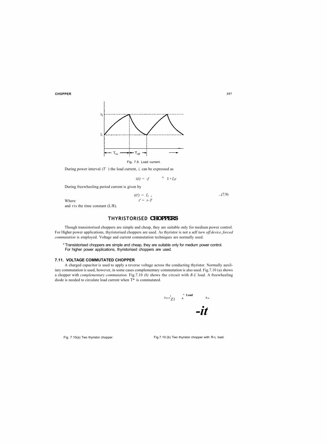
CHOPPER 357
Fig. 7.9. Load current.
During power interval (T ) the load current, i, can be expressed as
i(t) = -f A I +Ixe
During freewheeling period current is given by
Where and r is the time constant (L/R).
i(t') = I2 e
t' = t~T ...(7.9)
THYRISTORISED CHOPPERS Though transistorised choppers are simple and cheap, they are suitable only for medium power control.
For Higher power applications, thyristorised choppers are used. As thyristor is not a self turn off device, forced commutation is employed. Voltage and current commutation techniques are normally used.
* Transistorised choppers are simple and cheap, they are suitable only for medium power control. For higher power applications, thyristorised choppers are used.
7.11. VOLTAGE COMMUTATED CHOPPER A charged capacitor is used to apply a reverse voltage across the conducting thyristor. Normally auxil-
iary commutation is used, however, in some cases complementary commutation is also used. Fig.7.10 (a) shows a chopper with complementary commutation. Fig.7.10 (b) shows the circuit with R-L load. A freewheeling diode is needed to circulate load current when T* is commutated.
x ^ Load D p w Z l ^ R"
-it
Fig. 7.10(a) Two thyristor chopper. Fig.7.10.(b) Two thyristor chopper with R-L load.

362 POWER ELECTRONICS
Fig. 7.16. Single thyristor chopper.
Current commutation is achieved by injecting a reverse current, into a conducting thyristor, from a L-C resonant circuit.
Before triggering T, the capacitor is charged to a voltage (with the polarity shown in figure) through L and load. When J is triggered, it carries load current as well as the capacitor discharge current, iQ. Waveforms are shown in Fig. 7.18.
Fig. 7.18. Waveforms.

CHOPPER 363
Mode l.( tQ to tx): Discharge current is positive, hence, net current through thyristor is sum of the load current and discharge current.
Mode 2 ( tx to t2): In this mode discharge current flows in the reverse direction. At t2 thyristor current falls to zero and it is turned o f f .
Mode 3 (t2 to f 3 ) : In this mode constant load current flows through L and C. The capacitor is charged linearly and at t3, vcis equal to + V.
Mode 4(t3 to t4): As capacitor is charged to +Vs, D^ is forward biased and it begins to freewheel load current. Due to stored energy in the inductance, current through the capacitor continues to flow until r4, therefore, it is overcharged. After t4, Dm carries full load current. For a given load current, conduction period of the thyristor is constant. Output voltage can be varied by controlling the frequency of chopping.
7.17. MORGAN CHOPPER The Morgan chopper shown in Fig. 7.18 is also an example of single thyristor chopper. A saturable
reactor is used which behaves as a switch. In the linear region of B-Hcurve, magnetising current required by the reactor is negligible, therefore, inductance offered by it is very large. As a result, peak discharge current
Vs is negligible and the half time period, n V l C >*s verY large. When the reactor is positively or negatively
saturated then it offers very small inductance. Consequently, peak discharge current Vs is very large and half time period n^LsC is drastically reduced. Initially the capacitor is charged to + Vs through reactor and load. When 7 is turned on, it carries load current as well as discharge current.
In Morgan Chopper saturable reactor is used which behaves as a switch.
*DFW
Fig.7.18. Morgan chopper and its waveforms.


