Embed Size (px)
Citation preview

POWER DRIVER FOR BLDC/PMSM MOTORS INTEGRATED CIRCUITS
TRINAMIC Motion Control GmbH & Co. KG Hamburg, Germany
TMC6200 DATASHEET
FEATURES AND BENEFITS
3-phase motors up to 100A coil current (external MOSFETs)
Voltage Range 8 … 60V DC
Gate Drive Programmable 0.5A / 1A / 1.5A
Full Protection and Diagnostics via SPI interface
3 Floating Sense Amplifiers with programmable gain (5, 10, 20)
Gate Off Drive with 1Ω (LS) / 1.3Ω (HS) safe hold off resistance
SPI & Stand-Alone operation
Charge Pump for 100% Duty Cycle operation
Optional BBM break-before-make logic for single line control
Programmable Short and Overload current threshold and retry
Programmable Control Interface with 3 line or 6 line drive
Full Protection & Diagnostics
Compact Size TQFP48 package
Double Pin Distance for safe operation at high voltage
APPLICATIONS
PMSM FOC drives and BLDC motors Industrial Drives Factory Automation Lab Automation Robotics CNC machines Textile Machines Pumps Surveillance Cameras Home Automation Printers
DESCRIPTION
The TMC6200 is a high-power gate-driver for PMSM servo or BLDC motors. Using six external MOSFETs and two or three sense resistors, it integrates the full high voltage part of a PMSM drive system for 12V, 24V or 48V, including in-line current sense amplifiers with programmable amplification. It can drive a wide range of motors from Watt to Kilowatt. Software controlled drive strength allows in-system EME optimization. Programm-able safety features like short detection and overtemperature thresholds together with an SPI interface for diagnostics allow robust and reliable designs. With the TMC6200, a minimum number of external components is required to build a rugged drive with full protection and diagnostics.
Universal high voltage BLDC/PMSM/Servo MOSFET 3-halfbridge gate-driver with in line motor current sensing. External MOSFETs for up to 100A motor current.
BLOCK DIAGRAM

TMC6200 DATASHEET (Rev. 1.06 / 2020-JUN-10) 2
www.trinamic.com
APPLICATION EXAMPLES: PMSM AND BLDC MOTORS
The TMC6200 scores with integration of the complete high-voltage part for FOC controlled PMSM drivers. On the control side, it mates with sophisticated FOC TMC467x and TMC867x family controller chips, or with any microcontroller. Its versatile interface matches simple BLDC drives with minimum requirements on the µC PWM, as well as advanced PMSM control algorithms. The small form factor and easy-to-use package of the TMC6200 keeps costs down and allows for miniaturized layouts. Extensive support at the chip, board, and software levels enables rapid design cycles and fast time-to-market with competitive products. High integration and reliability deliver cost savings in related systems such as power supplies and cooling.
CPU TMC6200High-Level
Interface
Gate CTRL
MINIATURIZED CPU BASED DESIGN FOR BLDC OR PMSM
HIGH PERFORMANCE FOC SERVO DESIGN FOR PMSM
M
Encoder / Hall
DIAG
SPI (optional)
ADC
PWM
Current Sense
TMC6200
Gate CTRL
M
Encoder / Hall
SPI
Current Sense
CPU TMC467xADC
PWM
SPIHigh-Level Interface
ORDER CODES
Order code PN Description Size [mm2]
TMC6200-TA 00-0169 Three phase gate-driver for external MOSFETs; TQFP48 7 x 7 (body)
TMC6200-TA-T 00-0169-T -T denotes tape on reel packed devices
TMC6200-BOB 40-0164 Break out board board with TMC6200. 38 x 36
TMC6200-EVAL 40-0162 Evaluation board for TMC6200. 85 x 80
LANDUNGSBRÜCKE 40-0167 Baseboard for TMC6200-EVAL and further boards. 85 x 55
ESELSBRÜCKE 40-0098 Connector board for plug-in evaluation board system. 61 x 38
A CPU with internal BLDC or sine wave PWM unit drives the gate control lines based on encoder or hall sensor feedback. The current sensor outputs become sampled by the µC integrated ADC. Use of SPI is not required, unless more sophisticated diagnostics is desired.
When using one of the TRINAMIC FOC controllers, the CPU is completely offloaded from time-intensive regulation loop tasks, and software design shrinks to initialization and target parameter setting. The TMC6200 optimally complements a TMC467x family controller. The TMC6200-EVAL is part of TRINAMICs universal evaluation board system which provides a convenient handling of the hardware as well as a user-friendly software tool for evaluation. The TMC6200 evaluation board system consists of three parts: LANDUNGSBRÜCKE (base board), ESELSBRÜCKE (connector board including several test points), and TMC6200-EVAL, plus a TMC4671-EVAL FOC controller.

TMC6200 DATASHEET (Rev. 1.06 / 2020-JUN-10) 3
www.trinamic.com
Table of Contents
1 PRINCIPLES OF OPERATION ......................... 4
1.1 CONTROL INTERFACES ..................................... 6
2 PIN ASSIGNMENTS ........................................... 7
2.1 PACKAGE OUTLINE .......................................... 7 2.2 SIGNAL DESCRIPTIONS ................................... 7
3 SAMPLE CIRCUITS .......................................... 10
3.1 STANDARD APPLICATION CIRCUIT ................ 10 3.2 EXTERNAL GATE VOLTAGE REGULATOR .......... 11 3.3 ZERO STANDBY CURRENT .............................. 12 3.4 MOSFETS AND SLOPE CONTROL .................. 13 3.5 TUNING THE MOSFET BRIDGE ..................... 15
4 SPI INTERFACE ................................................ 18
4.1 SPI DATAGRAM STRUCTURE ......................... 18 4.2 SPI SIGNALS ................................................ 19 4.3 TIMING ......................................................... 20
5 REGISTER MAPPING ....................................... 21
5.1 GENERAL CONFIGURATION REGISTERS .......... 22
6 CURRENT SENSE AMPLIFIERS ..................... 27
6.1 SETTLING TIME ............................................. 27 6.2 CURRENT AMPLIFIER OFFSET ........................ 28 6.3 CHOICE OF SENSE RESISTORS ....................... 31
7 DIAGNOSTICS AND PROTECTION ............. 32
7.1 TEMPERATURE SENSORS ................................ 32
7.2 SHORT PROTECTION ...................................... 32
8 EXTERNAL RESET ............................................. 34
9 CLOCK OSCILLATOR AND INPUT ............... 34
9.1 USING THE INTERNAL CLOCK ........................ 34 9.2 USING AN EXTERNAL CLOCK ......................... 34
10 ABSOLUTE MAXIMUM RATINGS ............ 35
11 ELECTRICAL CHARACTERISTICS ............ 35
11.1 OPERATIONAL RANGE ................................... 35 11.2 DC AND TIMING CHARACTERISTICS .............. 36 11.3 THERMAL CHARACTERISTICS.......................... 40
12 LAYOUT CONSIDERATIONS..................... 41
12.1 EXPOSED DIE PAD ........................................ 41 12.2 WIRING GND .............................................. 41 12.3 WIRING BRIDGE SUPPLY .............................. 41 12.4 SUPPLY FILTERING ........................................ 41 12.5 LAYOUT EXAMPLE ......................................... 42
13 PACKAGE MECHANICAL DATA ................ 44
13.1 DIMENSIONAL DRAWINGS TQFP48-EP ....... 44 13.2 PACKAGE CODES ........................................... 45
14 DISCLAIMER ................................................. 46
15 ESD SENSITIVE DEVICE............................ 46
16 TABLE OF FIGURES .................................... 47
17 REVISION HISTORY ................................... 47

TMC6200 DATASHEET (Rev. 1.06 / 2020-JUN-10) 4
www.trinamic.com
1 Principles of Operation The TMC6200 is a MOSFET gate driver for three phase PMSM and BLDC motors. Ideally suited for applications in the range of 12V to 48V, it supports motor power ratings from 1 Watt to 1kW. It complements with TRINAMICs TMC467x & TMC867x families of three phase motor controller ICs. Internal break-before-make timing is provided for the ease-of-use in combination with simple microcontrollers for PWM generation. Integrated current sense amplifiers eliminate costly sense amplifiers required for FOC controllers (recommended use for applications up to 10A, use external precision amplifiers for higher current with low sense resistor values), while bringing the benefit of in-line current sensing. A complete set of protection and diagnostic functions makes the power stage more rugged than a discrete setup.
THE TMC6200 OFFERS TWO BASIC MODES OF OPERATION:
MODE 1: Stand-alone driver with pin configuration Enable this mode by tying low pin SPE. The interface pins allow a number of different settings for BBM generation and sense amplifier amplification control. MODE 2: SPI controlled This mode allows detailed control over the protection, diagnostic and control features, e.g. for tuning overcurrent detection. Enable this mode by tying high pin SPE.
VCC_IO
TMC62
00
Configuration interface
CSN / IDRV0
SCK / IDRV1
SDO / SINGLE
SDI / AMPLx10
Diagnostics(Short circuit, Temperature)
5V Regulator
Charge Pump
22n100V
100n 16V
FAULT
+VM
5VOUT
VSA
2.2µ+VIO
DRV_E
N
GNDA
DIE
PAD
3.3V or 5VI/O voltage
100n
100n
3 Phase Motor
Break before Make logic
100n
CE
IU IV
CURV
CURU
CURW
Current Sense
SPE
Enable
B.Dwersteg, ©
TRINAMIC 2014
LS
USENSE
LSU
HSU
UHS
CUCB
+VM
CPI
CPO
VCP
VS
Gate Voltage Regulator
12VOUT
4.7µ
470n
pd
pd
Sense Amplification 0: 5, 1: 10
0: xH/xL individual gate control1: xH=Polarity, xL=Enable control
WL
WH
VL
VH
UL
UH
pd
pd
pd
pd
pd
NS
RS
RP
12VOUT
I T
VCP
VOFS
LS
VSENSE
LSV
HSV
VHS
CVCB
RS
RP
12VOUT
VCP
LS
WSENSE
LSW
HSW
WHS
CWCB
RS
RP
12VOUT
VCP
I TI T
IV+
VOFS
IW+
5VOUT
VOFS
24MHz Oscillator
OTP memory
CLK_IN
+
500k
250k
VOFS
Chopper Control dual line LS+HS, or single line (HS=polarity, LS=enable)
+VIO
01
Diagnostic Output
Driver Strength [IDRV1 IDRV0]: 00: 0.5A 01: 0.5/1A, 10: 1A, 11: 1.5A
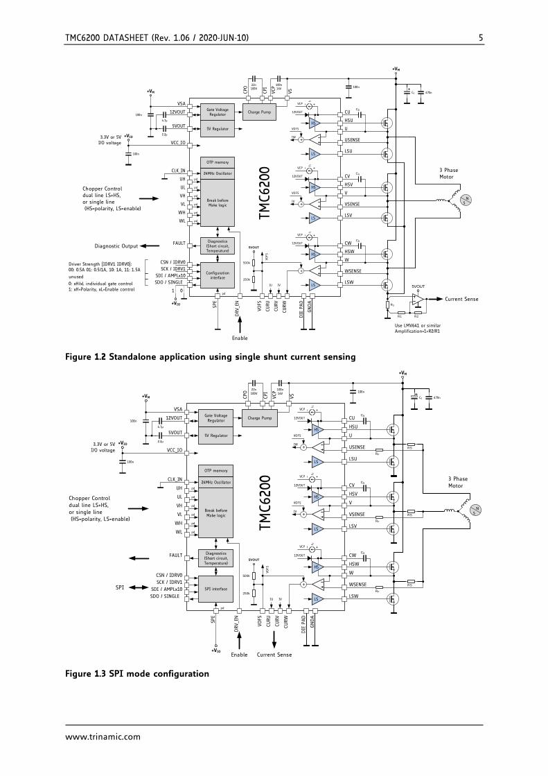
Figure 1.1 Standalone application using differential sensing
TMC6200 DATASHEET (Rev. 1.06 / 2020-JUN-10) 5
www.trinamic.com
VCC_IO
TMC62
00Configuration
interface
CSN / IDRV0
SCK / IDRV1
SDO / SINGLE
SDI / AMPLx10
Diagnostics(Short circuit, Temperature)
5V Regulator
Charge Pump
22n100V
100n 16V
FAULT
+VM
5VOUT
VSA
2.2µ+VIO
DRV_E
N
GNDA
DIE
PAD
3.3V or 5VI/O voltage
100n
100n
3 Phase Motor
Break before Make logic
100n
CE
IU IV
CURV
CURU
CURW
Current Sense
SPE
Enable
B.Dwersteg, ©
TRINAMIC 2014
LS
USENSE
LSU
HSU
UHS
CUCB
+VM
CPI
CPO
VCP
VS
Gate Voltage Regulator
12VOUT
4.7µ
470n
pd
pd
unused
0: xH/xL individual gate control1: xH=Polarity, xL=Enable control
WL
WH
VL
VH
UL
UH
pd
pd
pd
pd
pd
NS
12VOUT
I T
VCP
VOFS
LS
VSENSE
LSV
HSV
VHS
CVCB
12VOUT
VCP
LS
WSENSE
LSW
HSW
WHS
CWCB
12VOUT
VCP
I TI T
IV+
VOFS
IW+
5VOUT
VOFS
24MHz Oscillator
OTP memory
CLK_IN
+
500k
250k
VOFS
Chopper Control dual line LS+HS, or single line (HS=polarity, LS=enable)
+VIO
01
Diagnostic Output
Driver Strength [IDRV1 IDRV0]: 00: 0.5A 01: 0.5/1A, 10: 1A, 11: 1.5A
RS
R1 R2
5VOUT
Use LMV641 or similarAmplification=1+R2/R1
Figure 1.2 Standalone application using single shunt current sensing
VCC_IO
TMC62
00
SPI interface
CSN / IDRV0
SCK / IDRV1
SDO / SINGLE
SDI / AMPLx10
Diagnostics(Short circuit, Temperature)
5V Regulator
Charge Pump
22n100V
100n 16V
FAULT
+VM
5VOUT
VSA
2.2µ+VIO
DRV_E
N
GNDA
DIE
PAD
3.3V or 5VI/O voltage
100n
100n
3 Phase Motor
Break before Make logic
100n
CE
IU IV
CURV
CURU
CURW
SPE
B.Dwersteg, ©
TRINAMIC 2014
LS
USENSE
LSU
HSU
UHS
CUCB
+VM
CPI
CPO
VCP
VS
Gate Voltage Regulator
12VOUT
4.7µ
470n
pd
pdWL
WH
VL
VH
UL
UH
pd
pd
pd
pd
pd
NS
RS
RP
12VOUT
I T
VCP
VOFS
LS
VSENSE
LSV
HSV
VHS
CVCB
RS
RP
12VOUT
VCP
LS
WSENSE
LSW
HSW
WHS
CWCB
RS
RP
12VOUT
VCP
I TI T
IV+
VOFS
IW+
5VOUT
VOFS
24MHz Oscillator
OTP memory
CLK_IN
+
500k
250k
VOFS
+VIO
SPI
Current SenseEnable
Chopper Control dual line LS+HS, or single line (HS=polarity, LS=enable)
Figure 1.3 SPI mode configuration

TMC6200 DATASHEET (Rev. 1.06 / 2020-JUN-10) 6
www.trinamic.com
1.1 Control Interfaces The TMC6200 supports six control lines for the MOSFET drivers. High-side and low-side outputs can be individually controlled, or by an individual enable pin plus polarity pin, using internal BBM circuitry. An SPI interface or standalone configuration is supported.
1.1.1 Standalone Configuration Standalone configuration covers the most important settings like driver current and current amplifier amplification factor and the selection of internal or external BBM operation using four pins. Additional settings like BBM time and sensitivity of short detection can be modified using pre-programming via OTP memory, e.g. via an initial programming during product testing. This way, the driver can be fully operated and all protection mechanisms are in place. The fault output signals any critical driver error. It becomes cleared by disabling / re-enabling the driver. However, no advanced debugging is possible, like individual testing of failure mechanisms or setting a more sensitive temperature threshold. Also, it is not possible to switch to 20x current amplifier amplification.
Hint Standalone configuration is recommended for low-cost applications with small motors (e.g. motor current up to 10A RMS), where advanced debugging is not required or not possible. In case a sensitive overtemperature threshold must be set, or 20x current amplifier amplification is required due to high motor current, the SPI interface should be used.
1.1.2 SPI Interface The SPI interface is a bit-serial interface synchronous to a bus clock. For every bit sent from the bus master to the bus slave another bit is sent simultaneously from the slave to the master. Communication between an SPI master and the TMC6200 slave always consists of sending one 40-bit command word and receiving one 40-bit status word. The SPI command rate typically is a few commands for initialization or for diagnostic feedback.
Attention When operating in SPI mode, set drive mode (single line or individual control signals) first. For safety reasons, the driver starts up in single line mode. This setting will prevent operation if a controller operates the IC using individual control signals. Current amplifier amplification can be set within the same write access.

TMC6200 DATASHEET (Rev. 1.06 / 2020-JUN-10) 7
www.trinamic.com
2 Pin Assignments
2.1 Package Outline
25
26
37
24
DRV_EN
WH
1
CURW
UH
VC
C_
IO
SD
O_
SIN
GL
E
SD
I_A
MP
Lx1
0
SC
K_
IDR
V1
CS
N_
IDR
V0
FAULT
GNDA VSA
VH
2
3
4
5
6
7
8
9
10
11
14
15
16
17
18
19
20
21
22
23
36
35
34
33
32
31
30
29
28
27
48
47
46
45
44
43
42
41
40
39
38
13
5VOUT
PAD = GNDP, GNDD
12
VL
CL
K
SPE
TMC6200-TA
TQFP-48
CURV
CURU
UL
WU CV
HS
V
US
EN
SE
VS
EN
SE
V WS
EN
SE
HS
U
LSV
LSW
12VOUT
LSU
VCP
VS
CPI
CW
VOFS/TEST
WL
CPO
CU
HS
W
GNDP GNDP
GN
DD
Bernhard Dwersteg, TRINAMIC
Figure 2.1 TMC6200-TA pinning TQFP-EP 48 (7x7mm² body, 9x9mm² with leads)
2.2 Signal Descriptions
Pin TQFP Type Function
CU 1 Bootstrap capacitor positive connection. Tie to U terminal using 470nF to 1µF, 16V or 25V ceramic capacitor.
– 2, 28, 31, 35, 40, 45
N.C. Unused pins for increased creeping distances.
LSW 3 Low side gate driver output.
LSV 4 Low side gate driver output.

TMC6200 DATASHEET (Rev. 1.06 / 2020-JUN-10) 8
www.trinamic.com
Pin TQFP Type Function
LSU 5 Low side gate driver output.
12VOUT 6
Output of internal 11.5V gate voltage regulator and supply pin of low side gate drivers. Attach 2.2µF to 22µF ceramic capacitor to GND plane near to pin for best performance. Use at least 5-10 times more capacity than for bootstrap capacitors. In case an external gate voltage supply is available, tie VSA and 12VOUT to the external supply.
5VOUT 7 Output of internal 5V regulator. Attach 2.2µF to 10µF ceramic capacitor to GNDA near to pin for best performance.
GNDA 8 Analog GND. Connect to GND plane near pin.
CURU 9 AO Output of current sense amplifier.
CURV 10 AO Output of current sense amplifier.
CURW 11 AO Output of current sense amplifier.
VOFS/TEST 12 AI Center reference for current sense amplifiers (leave open for 5VOUT/3 offset voltage).
CSN_IDRV0 13 DI SPI chip select input (negative active) (SPE=1) or Configuration input for gate driver current LSB (SPE=0)
SCK_IDRV1 14 DI SPI serial clock input (SPE=1) or Configuration input for gate driver current MSB (SPE=0)
SDI_AMPLx10 15 DI SPI data input (SPE=1) or Configuration input for current sense amplifier 5x or 10x amplification (SPE=0)
SDO_SINGLE 16 DIO SPI data output (tristate) (SPE=1) or Configuration input for internal bridge control mode (0: dual line, 1: xH=phase polarity, xL=phase enable) (SPE=0)
UH 17 DI (pd)
High side control input (or bridge polarity in single mode)
UL 18 DI (pd)
Low side control input (or bridge enable in single mode)
VCC_IO 19 3.3V to 5V IO supply voltage for all digital pins.
VH 20 DI (pd)
High side control input (or bridge polarity in single mode)
VL 21 DI (pd)
Low side control input (or bridge enable in single mode)
WH 22 DI (pd)
High side control input (or bridge polarity in single mode)
WL 23 DI (pd)
Low side control input (or bridge enable in single mode)
CLK 24 DI CLK input. Tie to GND using short wire for internal clock or supply external clock. Internal clock-fail over circuit protects against loss of external clock signal.
SPE 25 DI (pd)
Mode selection input. When tied low, the chip is in standalone mode and SPI pins have their configuration pin functions. When tied high, the SPI interface is enabled. Integrated pull down resistor.
FAULT 26 DO Diagnostics output. High upon driver error condition. Clear by cycling EN.
DRV_EN 27 DI Positive active enable input. The power stage becomes switched off (all motor outputs floating) when this pin becomes driven to a low level. Cycle low to clear FAULT.
VSA 29 Analog supply voltage for 11.5V and 5V regulator. Normally tied to VS. Provide a 100nF filtering capacitor to GND.
CPO 30 Charge pump capacitor output.

TMC6200 DATASHEET (Rev. 1.06 / 2020-JUN-10) 9
www.trinamic.com
Pin TQFP Type Function
CPI 32 Charge pump capacitor input. Tie to CPO using 22nF 100V capacitor. In case ringing of the power supply leads to considerable supply ripple, add a 10-22Ohm series resistor.
VS 33 Motor supply voltage. Provide filtering capacity near pin with short loop to GND plane. Must be tied to the positive bridge supply voltage. Severe ringing must be avoided.
VCP 34 Charge pump voltage. Tie to VS using 100nF capacitor.
CW 36 Bootstrap capacitor positive connection. Tie to W terminal using 470nF to 1µF, 16V or 25V ceramic capacitor.
HSW 37 High side gate driver output.
W 38 Bridge center and bootstrap capacitor negative connection. Connect to source pin of HS-MOSFET.
WSENSE 39 AI
Sense resistor connection for phase W. Connect to the motor side of the sense resistor. A 10Ω to 22Ω protection resistor is recommended. Directly connect to W, in case no sense resistor is used.
VSENSE 41 AI
Sense resistor connection for phase V. Connect to the motor side of the sense resistor. A 10Ω to 22Ω protection resistor is recommended. Directly connect to V, in case no sense resistor is used.
V 42 Bridge center and bootstrap capacitor negative connection. Connect to source pin of HS-MOSFET.
HSV 43 High side gate driver output.
CV 44 Bootstrap capacitor positive connection. Tie to V terminal using 470nF to 1µF, 16V or 25V ceramic capacitor.
USENSE 46 AI
Sense resistor connection for phase U. Connect to the motor side of the sense resistor. A 10Ω to 22Ω protection resistor is recommended. Directly connect to U, in case no sense resistor is used.
U 47 Bridge center and bootstrap capacitor negative connection. Connect to source pin of HS-MOSFET.
HSU 48 High side gate driver output.
Exposed die pad
-
Connect the exposed die pad to a GND plane. Provide as many as possible vias for heat transfer to GND plane. Serves as GND pin for the low side gate drivers and for digital logic. Ensure low loop inductivity to sense resistor GND.
*(pd) denominates a pin with pulldown resistor

TMC6200 DATASHEET (Rev. 1.06 / 2020-JUN-10) 10
www.trinamic.com
3 Sample Circuits The following sample circuits show the required external components in different operation and supply modes. The connection of the bus interface and further digital signals are left out for clarity.
3.1 Standard Application Circuit
VCC_IO
TMC62
00
SPI interface
CSN / IDRV0
SCK / IDRV1
SDO / SINGLE
SDI / AMPLx10
Diagnostics(Short circuit, Temperature)
5V Regulator
Charge Pump
22n100V
100n 16V
FAULT
+VM
5VOUT
VSA
2.2µ+VIO
DRV_E
N
GNDA
DIE
PAD
3.3V or 5VI/O voltage
100n
100n
3 Phase Motor
Break before Make logic
100n
CE
Optional use lower
voltage down to 12V
Use low inductivity SMD
type, e.g. 1210 or 2512
resistor for RS!
IU IV
CURV
CURU
CURW
Current Sense outputs
SPE
Driver Enable (positive active)
B.Dwersteg, ©
TRINAMIC 2014
LS
USENSE
LSU
HSU
UHS
CUCB
+VM
GND: Stand alone, VIO: SPI interface mode
CPI
CPO
VCP
VS
Gate Voltage Regulator
12VOUT
4.7µ
Bootstrap capacitors CB:
For MOSFETs with QG<40nC: min. 470nF, 16V
1µF for larger QG - use minimum 4.7µF on 12VOUT pin
470n
Keep inductivity of the fat
interconnections as small as
possible to avoid undershoot
of U/V/W < -5V!
RG
RG
Optional slope control resistors RG:
In case of MOSFETs <20nC, adapt to MOSFET to yield slopes of
roughly 50ns. Slope must be slower than bulk diode recovery time.
1Ohm to 2.2Ohm recommended for larger MOSFETs.
May be left away with compact, low inducivity routing of power stage.
+VIO
pd
pd
+VIO
Driver Strength [IDRV1 IDRV0]: 00: 0.5A 01: 0.5/1A, 10: 1A, 11: 1.5A
Settings in Standalone mode (SPE=0)
Sense Amplification 0: 5*, 1: 10*
0: xH/xL individual gate control1: xH=Polarity, xL=Enable control
WL
WH
VL
VH
UL
UH
pd
pd
pd
pd
pd
NS
RS
RP
RP (optional 10 Ohm to 22
Ohm) protects the sense
amplifier against excessive
spikes on RS
12VOUT
I T
VCP
VOFS
LS
VSENSE
LSV
HSV
VHS
CVCB
RG
RG
RS
RP
12VOUT
VCP
LS
WSENSE
LSW
HSW
WHS
CWCB
RG
RG
RS
RP
12VOUT
VCP
I TI T
IV+
VOFS
IW+
5VOUT
VOFS
24MHz Oscillator
OTP memory
CLK_IN
+
500k
250k
VOFS
SPI interface (SPE=1)
Figure 3.1 Standard application circuit
The standard application circuit uses a minimum set of additional components. Six MOSFETs are selected for the desired current, voltage and package type. Two or three sense resistors are matched to the maximum motor coil current, and to the desired current sensor output swing and amplification setting. See chapter 0 to choose the right value for sense resistors. Use low ESR capacitors for filtering the power supply. A minimum capacity of 100µF per ampere of coil current near to the power bridge is recommended for keeping power supply ripple low. The capacitors need to cope with the current ripple caused by chopper operation. Current ripple in the supply capacitors also depends on the power supply internal resistance and cable length. Supply VCC_IO from 5VOUT, or from an external source, e.g. a 3.3V regulator. In order to minimize linear voltage regulator power dissipation of the internal 5V and 11.5V voltage regulators in applications where VM is high, a different (lower) supply voltage should be used for VSA, when available (see chapter 3.2).
Important layout hints Place sense resistors and all filter capacitors as close as possible to the power MOSFETs. Place the TMC6200 near to the MOSFETs and use short interconnection lines in order to minimize parasitic trace inductance. Use a solid common GND for all GND and GNDA connections. Connect 5VOUT filtering capacitor directly to 5VOUT and GNDA pin. See layout hints for more details. Low ESR electrolytic capacitors are recommended for VS filtering.

TMC6200 DATASHEET (Rev. 1.06 / 2020-JUN-10) 11
www.trinamic.com
Attention In case VSA is supplied by a different voltage source, make sure that VSA does not drop out during motor operation. The motor driver should be disabled in case VSA becomes switched off before VS. Hard switching edges on VSA might result in bridge cross-conduction otherwise. It is safest to derive VSA voltage from VS supply.
Attention Make sure, that VCC_IO does not drop out during operation of the motor. Disable the drive when a falling supply voltage is detected. It is safest to derive VCC_IO voltage from VS supply.
Hint Production devices use VCC_IO undervoltage detection to disable the MOSFET drivers. This will avoid motor overcurrent due to instable input levels during power-up / power-down for most cases. However, it is best practice to disable the motor prior to switching off power supply, and to make sure, that the motor power supply does come up without or not remain with missing VCC_IO supply. Initial devices dated 1836 do not yet implement this VCC_IO controlled undervoltage reset of the drivers.
3.2 External Gate Voltage Regulator At high supply voltages like 48V, the internal gate voltage regulator and the internal 5V regulator have considerable power dissipation, especially with high MOSFET gate charges or high chopper frequency. A good thermal coupling of the heat slug to the system PCB GND plane is required to dissipate heat. Still, the thermal thresholds will be lowered significantly by self-heating. To reduce power dissipation, supply an external gate driver voltage to the TMC6200. Figure 3.2 shows the required connection. The internal gate voltage regulator becomes disabled in this constellation. 12V +/-1V is recommended for best results.
12V Gate Voltage
Supply
5V Regulator
+VG
5VOUT
VSA
2.2µ
100n
Gate Voltage Regulator
12VOUT
Figure 3.2 External gate voltage supply
Hint With MOSFETs above 50nC of total gate charge or chopper frequency >40kHz, it is recommended to use a VSA supply not higher than 40V in order to keep reasonable power dissipation.

TMC6200 DATASHEET (Rev. 1.06 / 2020-JUN-10) 12
www.trinamic.com
3.3 Zero Standby Current Battery powered applications often require low current standby, while keeping the supply switched on. The TMC6200 can support these applications by completely powering down the control side, VSA, and with this also the charge pump and 5V supply. See Figure 3.3 for an example using a P-MOSFET as high-side switch. Gate charge / discharge is limited to avoid too steep slopes and excess current. VCC_IO may remain active during standby operation. Make sure that the motor becomes disabled before switching off the power supply!
5V Regulator
Gate Voltage Regulator
5VOUT
NSTANDBY0V=standby
3-5V for operation
2.2µ
100n12VOUT
4.7µ
+VM
BC546
100n22k
10k
BSS84
VSA
Figure 3.3 Standby Switch
Hint Realize zero standby current by switching off VSA in standby mode. VCC_IO may remain active. Ensure a slope-controlled power-up of 1V/µs or less to avoid excess current into VSA.
Attention Test your circuit thoroughly in order to ensure a safe and clean power-up and standby power-up and power-down event! When powering down the control side of the MOSFET drivers, MOSFET gate-off is only ensured by high-resistive resistors within the TMC6200. This makes the circuit more susceptible to injection of charge from MOSFET drain to gate, e.g. to high supply voltage slopes. Any spurious cross-conduction could lead to destructive currents through the power MOSFETs.

TMC6200 DATASHEET (Rev. 1.06 / 2020-JUN-10) 13
www.trinamic.com
3.4 MOSFETs and Slope Control The selection of power MOSFETs depends on a number of factors, like package size, on-resistance, voltage rating and supplier. It is not true, that larger, lower RDSon MOSFETs will always be better, as a larger device also has higher capacitances and may add more ringing in trace inductance and power dissipation in the gate drive circuitry. Adapt the MOSFETs to the required motor voltage (adding 5-10V of reserve to the peak supply voltage) and to the desired maximum current, in a way that resistive power dissipation still is low for the chosen MOSFET package. The TMC6200 drives the MOSFET gates with roughly 10V, so normal, 10V specified types are sufficient. Logic level FETs (4.5V specified RDSon) will also work but may be more critical with regard to bridge cross-conduction due to lower VGS(th). The gate-drive current and MOSFET gate resistors RG (optional) should basically be adapted to the MOSFET gate-drain charge (Miller charge) in order to yield reasonable slope times. Figure 3.4 shows the influence of the Miller charge on the switching event. Figure 3.5 additionally shows the switching events in different load situations (load pulling the output up or down), and the required bridge brake-before-make time. The following table shall serve as a thumb rule for programming the MOSFET driver current (DRVSTRENGTH setting) and the selection of gate resistors:
MOSFET MILLER CHARGE VS. DRVSTRENGTH AND RG
Miller Charge [nC] (typ.)
DRVSTRENGTH setting
Value of RG [Ω]
<10 0 or 1 ≤ 10 (recommended)
10…20 0 to 2 ≤ 5 (optional)
20…80 1 to 3 ≤ 2.5 (optional)
>80 3 ≤ 1 (optional)
The TMC6200 provides increased gate-off drive current to avoid bridge cross-conduction induced by high dV/dt. This protection will be less efficient with gate resistors exceeding the values given in the table. For larger values of RG, a parallel diode may be required to ensure keeping the MOSFET safely off during switching events of the opposite MOSFET.
MOSFET gate charge vs. switching event
QG – Total gate charge (nC)
VGS –
Gat
e to s
ourc
e v
oltag
e (V)
10
8
6
4
2
00 5 10 15 20 25
VDS –
Dra
in to s
ourc
e v
oltag
e (V)
25
20
15
10
5
0
VM
QMILLER
Figure 3.4 Miller charge determines switching slope
Hints
- Choose modern MOSFETs with fast and soft recovery bulk diode and low reverse recovery charge.
- A small, SMD MOSFET package allows compacter routing and reduces parasitic inductance effects.

TMC6200 DATASHEET (Rev. 1.06 / 2020-JUN-10) 14
www.trinamic.com
MOSFE
T drive
rsLx
BMx
Hx
0V
V12VOUT
0V
0V
VVM
VVM+V12VOUT
VVM
Load pulling BMx down Load pulling BMx up
tBBMtBBM
Miller plateau
Hx-BMx
0V
VCX-VBMx Miller plateau
Effective break-before-make time
-1.2V
Output slope
Output slope
tBBM
Figure 3.5 Slopes, Miller plateau and blank time (BMx=U V or W output)
The following DRV_CONF parameters allow adapting the driver to the MOSFET bridge:
Parameter Description Setting Comment
BBMCLKS
Break-before-make time setting to ensure non-overlapping switching of high-side and low-side MOSFETs. Digital BBM time in clock cycles (typ. 42ns/CLK). BBMCLKS is used in combination with singleline=1. It is not applicable with individual LS and HS signals. Additionally, a minimum BBM time of 75ns is enforced by analog circuitry even with individual control signals. This prevents short-circuiting of the bridge
0…15 time[ns] 42ns*BBMCLKS Ensure ~30% headroom Reset Default: OTP 1..4 4, when not programmed
DRV_ STRENGTH
Selection of gate driver current. Adapts the gate driver current to the gate charge of the external MOSFETs.
0…3 Reset Default = 2 in SPI mode
DRV_CONF Parameters Use the lowest gate driver strength setting DRV_STRENGTH giving favorable switching slopes, before increasing the value of the gate series resistors. A slope time of nominal 40ns to 80ns is absolutely sufficient and will normally be covered by a Break-Before-Make time setting of 1 to 4 (4 is default). In case slower slopes have to be used, e.g. with large MOSFETs, ensure that the break-before-make time sufficiently covers the switching event, in order to avoid bridge cross conduction. The shortest break-before-make time, safely covering the switching event, gives best results. Add roughly 30% of reserve, to cover production stray of MOSFETs and driver.

TMC6200 DATASHEET (Rev. 1.06 / 2020-JUN-10) 15
www.trinamic.com
3.5 Tuning the MOSFET Bridge A clean switching event is favorable to ensure low power dissipation and good EMC behavior. Unsuitable layout or components endanger stable operation of the circuit. Therefore, it is important to understand the effect of parasitic trace inductivity and MOSFET reverse recovery. Stray inductance in power routing will cause ringing whenever the opposite MOSFET is in diode conduction prior to switching on a low-side or high-side MOSFET. Diode conduction occurs during break-before make time whenever the load current is inverse to the following bridge polarity. The MOSFET bulk diode has a certain, type specific reverse recovery time and charge. This time typically is in the range of a few 10ns. During reverse recovery time, the bulk diode will cause high current flow across the bridge. This current is taken from the power supply filter capacitors (see thick lines Figure 3.6). Once the diode opens, parasitic inductance tries to keep the current flowing. A high, fast slope results and leads to ringing in all parasitic inductivities (see Figure 3.7). This may lead to bridge voltage undershooting the GND level as well as fast pulses on VS and all MOSFET connections. It must be ensured, that the driver IC does not see spikes on its BM pins to GND going below -5V. Severe VS ripple might overload the charge-pump circuitry. Measure the voltage directly at the driver pins to driver GND. The amount of undershooting depends on energy stored in parasitic inductivities from low side drain to low side source and via the sense resistor RS to GND. When using relatively small MOSFETs, a soft slope control requires a high gate series resistance. This endangers safe MOSFET switch off. Add additional diodes to ensure safe MOSFET off conditions with slow switch-on slopes (Figure 3.10).
GNDA
DIE
PAD
LS
VSENSE
LSV
HSV
VHS
CV
CB
+VM
RG: Reduce slope and protect the driver against ringing
in the interconnections between MOSFET and driver
4.7µF
RG
RG
Coil out
RG
Decide use and value of the additional components based on measurements of the actual circuit using
the final layout!
1n, 100V
470pF to a few nF output
capacitors close to bridge
and / or output reduce
ringing and improve EMC
Additional 1A type Schottky Diodes (selected for full VM range) in
combination with RG to 1 Ohm) eliminate undershooting of BM.
RP
RS
RP: Protects the sense input
against undershooting in case of
high inductance of the sense
resistor or connections
LOW-
ESR
Place filtering capacitors near to the bridge to avoid
severe overshooting and ringing.
Use sufficient capacitance with regard to motor current.
VS
220nF1R
Optional RC filter
against VS ringing
Figure 3.6 Bridge protection options for power routing inductivity

TMC6200 DATASHEET (Rev. 1.06 / 2020-JUN-10) 16
www.trinamic.com
ENSURE RELIABLE OPERATION
- Use SMD MOSFETs and short interconnections
- Provide sufficient power filtering capacity close to the bridge and close to VS pin
- Tune MOSFET switching slopes (measure switch-on event at MOSFET gate) to be slower than the MOSFET bulk diode reverse recovery time. This will reduce cross conduction.
- Add optional gate resistors close to MOSFET gate and output capacitors to ensure clean switching and reliable operation by minimizing ringing. Figure 3.6 shows the options plus some variations.
- Some MOSFETs eliminate reverse recovery charge by integrating a fast diode from source to drain.
Figure 3.7 Ringing of output (green) and Gate voltages (yellow, blue) with DRVSTRENGTH=0
Figure 3.8 Ringing of output (green) and Gate voltages (yellow, blue) with DRVSTRENGTH=2
Figure 3.9 Ringing of output (green) and Gate voltages (yellow, blue) with DRVSTRENGTH=3

TMC6200 DATASHEET (Rev. 1.06 / 2020-JUN-10) 17
www.trinamic.com
BRIDGE OPTIMIZATION EXAMPLE
A driver for 15A, 60V has been designed using the MOSFET BSC037N08NS (3.7mΩ, 80V, QG=56nC, tRR=41ns) in the standard schematic. The MOSFETs offer roughly 20ns slope time at the lowest driver strength setting. Switching quality is good and signals are clean (Figure 3.7, ff.). At double drive strength, the slope time halves, and switching events still are clean. When increasing to full gate drive strength faster slopes lead to increased ringing on all signals. Low or medium slope setting is best. Additional gate resistors or 1nF output capacitors do not bring any additional improvement. The layout already proves to be good. No additional components were required!
GNDA
DIE
PAD
LS
VSENSE
LSV
HSV
VHS
CV
CB
+VM
4.7µF
RG
RG
Coil out
Additional 1A type Schottky Diodes (20V type sufficient) in
combination with high resistance gate resistors >10Ohm
RP
RS
LOW-
ESR
VS
220nF
Figure 3.10 Diodes for safe off condition with high gate series resistance
BRIDGE LAYOUT CONSIDERATIONS
- Tune the bridge layout for minimum loop inductivity. A compact layout is best.
- Keep MOSFET gate connections short and straight and avoid loop inductivity between bridge feedback (U,V,W) and corresponding HS driver pin. Loop inductance is minimized with parallel traces, or adjacent traces on adjacent layers. A wider trace reduces inductivity (don’t use minimum trace width).
- Place the TMC6200 near the low side MOSFETs GND connections, with its GND connections directly connected to the same GND plane.
- Optimize switching behavior by using lowest acceptable gate current setting.
- Check influence of optional components shown in Figure 3.6.
- Measure the performance of the bridge by probing BM pins directly at the bridge or at the TMC6200 using a short GND tip on the scope probe rather than a GND cable, if available.
TMC6200 DATASHEET (Rev. 1.06 / 2020-JUN-10) 18
www.trinamic.com
4 SPI Interface
4.1 SPI Datagram Structure The TMC6200 uses 40 bit SPI™ (Serial Peripheral Interface, SPI is Trademark of Motorola) datagrams for communication with a microcontroller. Microcontrollers which are equipped with hardware SPI are typically able to communicate using integer multiples of 8 bit. The NCS line of the device must be handled in a way, that it stays active (low) for the complete duration of the datagram transmission. Each datagram sent to the device is composed of an address byte followed by four data bytes. This allows direct 32 bit data word communication with the register set. Each register is accessed via 32 data bits even if it uses less than 32 data bits. For simplification, each register is specified by a one-byte address:
- For a read access the most significant bit of the address byte is 0. - For a write access the most significant bit of the address byte is 1.
Read and write functionality of the individual registers may differ.
4.1.1 Selection of Write / Read (WRITE_notREAD) The read and write selection is controlled by the MSB of the address byte (bit 39 of the SPI datagram). This bit is 0 for read access and 1 for write access. So, the bit named W is a WRITE_notREAD control bit. The active high write bit is the MSB of the address byte. So, 0x80 has to be added to the address for a write access. The SPI interface always delivers data back to the master, independent of the W bit. Read data coming back in a write access should be ignored.
Read data is transferred back to the master directly in the read access. Internal read access occurs during the transmission in the moment when the address bits have been received.
Example:
For a read access to the register (GSTAT) with the address 0x00, the address byte has to be set to 0x00. For a write access to the register (GCONF), the address byte has to be set to 0x80 + 0x01 = 0x81. For read access, the data bits don’t care. So, one can set them to 0. action data sent to TMC6200 data received from TMC6200 read GSTAT → 0x0100000000 AA & GSTAT
write GCONF:= 0x00000010 → 0x8000000010 0x01 & unused
*)AA: is a placeholder for the address byte used in the previous access
SPI DATAGRAM STRUCTURE
MSB (transmitted first) 40 bit LSB (transmitted last)
39 ... ... 0
→ 8 bit address 8 bit SPI status
→ 32 bit data
39 ... 32 31 ... 0
→ to TMC6200
RW + 7 bit address
from TMC6200
unused
8 bit data 8 bit data 8 bit data 8 bit data
39 / 38 ... 32 31 ... 24 23 ... 16 15 ... 8 7 ... 0 W 38...32 31...28 27...24 23...20 19...16 15...12 11...8 7...4 3...0
39
38
37
36
35
34
33
32
31
30
29
28
27
26
25
24
23
22
21
20
19
18
17
16
15
14
13
12
11
10
9 8 7 6 5 4 3 2 1 0

TMC6200 DATASHEET (Rev. 1.06 / 2020-JUN-10) 19
www.trinamic.com
4.1.2 Data Alignment All data are right aligned. Some registers represent unsigned (positive) values, some represent integer values (signed) as two’s complement numbers, single bits or groups of bits are represented as single bits respectively as integer groups.
4.2 SPI Signals The SPI bus on the TMC6200 has four signals:
- SCK – bus clock input - SDI – serial data input - SDO – serial data output - CSN – chip select input (active low)
The slave is enabled for an SPI transaction by a low on the chip select input CSN. Bit transfer is synchronous to the bus clock SCK, with the slave latching the data from SDI on the rising edge of SCK and driving data to SDO following the falling edge. The most significant bit is sent first. A minimum of 40 SCK clock cycles is required for a bus transaction with the TMC6200.
The TMC6200 does not allow cascading of SPI slaves. Use individual CSN lines for each device.
CSN must be low during the whole bus transaction. When CSN goes high, the contents of the internal shift register are latched into the internal control register and recognized as a command from the master to the slave.

TMC6200 DATASHEET (Rev. 1.06 / 2020-JUN-10) 20
www.trinamic.com
4.3 Timing The SPI interface is synchronized to the internal system clock, which limits the SPI bus clock SCK to 1/4 of the system clock frequency. If the system clock is based on the on-chip oscillator, an additional 10% safety margin must be used to ensure reliable data transmission. All SPI inputs as well as the ENN input are internally filtered to avoid triggering on pulses shorter than 20ns. Figure 4.1 shows the timing parameters of an SPI bus transaction, and the table below specifies their values.
CSN
SCK
SDI
SDO
tCC tCCtCL tCH
bit39 bit38 bit0
bit39 bit38 bit0
tDO tZC
tDU tDH
tCH
Figure 4.1 SPI timing
Hint Usually this SPI timing is referred to as SPI MODE 3
SPI interface timing AC-Characteristics
clock period: tCLK
Parameter Symbol Conditions Min Typ Max Unit
SCK valid before or after change of CSN
tCC
10 ns
CSN high time tCSH
*) Min time is for synchronous CLK with SCK high one tCH before CSN high only
tCLK*) >2tCLK+10 ns
SCK low time tCL *) Min time is for synchronous CLK only
tCLK*) >tCLK+10 ns
SCK high time tCH *) Min time is for synchronous CLK only
tCLK*) >tCLK+10 ns
SCK frequency using internal clock
fSCK assumes minimum OSC frequency 3.5 MHz
SCK frequency using external clock
fSCK assumes synchronous CLK fCLK/6 MHz
SDI setup time before rising edge of SCK
tDU
10 ns
SDI hold time after rising edge of SCK
tDH
10 ns
Data out valid time after falling SCK clock edge
tDO no capacitive load on SDO tCLK+10 ns
SDI, SCK and CSN filter delay time
tFILT rising and falling edge 12 20 30 ns

TMC6200 DATASHEET (Rev. 1.06 / 2020-JUN-10) 21
www.trinamic.com
5 Register Mapping This chapter gives an overview of the complete register set. Some of the registers bundling a number of single bits are detailed in extra tables. The functional practical application of the settings is detailed in dedicated chapters.
Note - All registers become reset to 0 upon power up, unless otherwise noted. - Add 0x80 to the address Addr for a write access!
NOTATION OF HEXADECIMAL AND BINARY NUMBERS
0x precedes a hexadecimal number, e.g. 0x04
% precedes a multi-bit binary number, e.g. %100
NOTATION OF R/W FIELD
R Read only
W Write only
R/W Read- and writable register
R+WC Clear upon write back with ‘1’
OVERVIEW REGISTER MAPPING
REGISTER DESCRIPTION
General Configuration Registers These registers contain
- global configuration
- global status flags
- interface configuration
- driver configuration
- OTP programming
TMC6200 DATASHEET (Rev. 1.06 / 2020-JUN-10) 22
www.trinamic.com
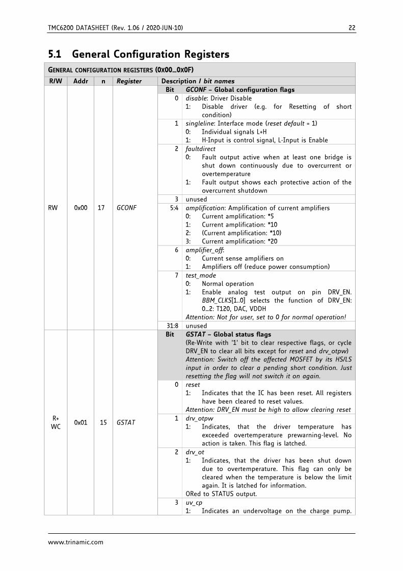
5.1 General Configuration Registers
GENERAL CONFIGURATION REGISTERS (0X00…0X0F)
R/W Addr n Register Description / bit names
RW 0x00 17 GCONF
Bit GCONF – Global configuration flags
0 disable: Driver Disable 1: Disable driver (e.g. for Resetting of short
condition)
1 singleline: Interface mode (reset default = 1) 0: Individual signals L+H 1: H-Input is control signal, L-Input is Enable
2 faultdirect 0: Fault output active when at least one bridge is
shut down continuously due to overcurrent or overtemperature
1: Fault output shows each protective action of the overcurrent shutdown
3 unused
5:4 amplification: Amplification of current amplifiers 0: Current amplification: *5 1: Current amplification: *10 2: (Current amplification: *10) 3: Current amplification: *20
6 amplifier_off: 0: Current sense amplifiers on 1: Amplifiers off (reduce power consumption)
7 test_mode 0: Normal operation 1: Enable analog test output on pin DRV_EN.
BBM_CLKS[1..0] selects the function of DRV_EN: 0…2: T120, DAC, VDDH
Attention: Not for user, set to 0 for normal operation!
31:8 unused
R+ WC
0x01 15 GSTAT
Bit GSTAT – Global status flags (Re-Write with ‘1’ bit to clear respective flags, or cycle DRV_EN to clear all bits except for reset and drv_otpw) Attention: Switch off the affected MOSFET by its HS/LS input in order to clear a pending short condition. Just resetting the flag will not switch it on again.
0 reset 1: Indicates that the IC has been reset. All registers
have been cleared to reset values. Attention: DRV_EN must be high to allow clearing reset
1 drv_otpw 1: Indicates, that the driver temperature has
exceeded overtemperature prewarning-level. No action is taken. This flag is latched.
2 drv_ot 1: Indicates, that the driver has been shut down
due to overtemperature. This flag can only be cleared when the temperature is below the limit again. It is latched for information.
ORed to STATUS output.
3 uv_cp 1: Indicates an undervoltage on the charge pump.

TMC6200 DATASHEET (Rev. 1.06 / 2020-JUN-10) 23
www.trinamic.com
GENERAL CONFIGURATION REGISTERS (0X00…0X0F)
R/W Addr n Register Description / bit names
The driver is disabled during undervoltage. This flag is latched for information.
ORed to STATUS output.
4 shortdet_u 1: U short counter has triggered at least once. ORed to STATUS output.
5 s2gu 1: Short to GND detected on phase U. The driver
becomes disabled until flag becomes cleared. ORed to STATUS output.
6 s2vsu 1: Short to VS detected on phase U. The driver
becomes disabled until flag becomes cleared. ORed to STATUS output.
7 -
8 shortdet_v 1: V short counter has triggered at least once. ORed to STATUS output.
9 s2gv 1: Short to GND detected on phase V. The driver
becomes disabled until flag becomes cleared. ORed to STATUS output.
10 s2vsv 1: Short to VS detected on phase V. The driver
becomes disabled until flag becomes cleared. ORed to STATUS output.
11 -
12 shortdet_w 1: short counter has triggered at least once. ORed to STATUS output.
13 s2gw 1: Short to GND detected on phase W. The driver
becomes disabled until flag becomes cleared. ORed to STATUS output.
14 s2vsw 1: Short to VS detected on phase W. The driver
becomes disabled until flag becomes cleared. ORed to STATUS output.
R 0x04 8 + 8
IOIN
Bit INPUT
Reads the state of all input pins available
0 UL
1 UH
2 VL
3 VH
4 WL
5 WH
6 DRV_EN
7 0
8 OTPW
9 OT136°C
10 OT143°C

TMC6200 DATASHEET (Rev. 1.06 / 2020-JUN-10) 24
www.trinamic.com
GENERAL CONFIGURATION REGISTERS (0X00…0X0F)
R/W Addr n Register Description / bit names
11 OT150°C
31.. 24
VERSION: 0x10=first version of the IC Identical numbers mean full digital compatibility.
W 0x06 OTP_PROG
Bit OTP_PROGRAM – OTP programming Write access programs OTP memory (one bit at a time), Read access refreshes read data from OTP after a write
2..0 OTPBIT Selection of OTP bit to be programmed to the selected byte location (n=0..7: programs bit n to a logic 1)
5..4
OTPBYTE Set to 00
15..8 OTPMAGIC Set to 0xbd to enable programming. A programming time of minimum 10ms per bit is recommended (check by reading OTP_READ).
R 0x07 OTP_READ
Bit OTP_READ (Access to OTP memory result and update) See table 5.1.1!
7..0 OTP0 byte 0 read data
RW 0x08 5 FACTORY_ CONF
4..0 FCLKTRIM (Reset default: OTP) 0…31: Lowest to highest clock frequency. Check at charge pump output. The frequency span is not guaranteed, but it is tested, that tuning to 12MHz internal clock is possible. The devices come preset to 12MHz clock frequency by OTP programming. (Reset Default: OTP)
RW 0x09 19 SHORT_ CONF
Bit SHORT_CONF
3..0 S2VS_LEVEL: Short to VS detector level for lowside FETs. Checks for voltage drop in LS MOSFET and opt. bottom shunt. 1 (highest sensitivity) … 15 (lowest sensitivity) (Reset Default: OTP 6 or 12)
11..8 S2G_LEVEL: Short to GND detector level for highside FETs. Checks for voltage drop on high side MOSFET 2 (highest sensitivity) … 15 (lowest sensitivity) Hint: Use high setting. For sensitive overcurrent protection, tune S2VS level instead. (Reset Default: OTP 6 or 12)
17..16 SHORTFILTER: Spike filtering bandwidth for short detection 0 (lowest, 100ns), 1 (1µs), 2 (2µs) 3 (3µs) Hint: Increase value, if erroneous short detection occurs. (Reset Default = %01)
20 shortdelay: Short detection delay 0=750ns: normal, 1=1500ns: high The short detection delay shall cover the bridge switching time. 0 will work for most applications. (Reset Default = 0)
TMC6200 DATASHEET (Rev. 1.06 / 2020-JUN-10) 25
www.trinamic.com
GENERAL CONFIGURATION REGISTERS (0X00…0X0F)
R/W Addr n Register Description / bit names
25..24 RETRY: Number of retries for short detection 0: Half bridge disabled after first short detection 1..3: Half bridge re-enabled in next chopper cycles 1
time to 3 times. With retry, the short-counter is decreased once each 256 chopper cycles per coil, unless the upper limit has been reached.
(Reset Default = 3)
28 protect_parallel 0: Only the detected half bridge driver becomes
shut down upon final short detection 1: All half bridge drivers become shut down upon
final short detection (Reset Default = 1)
29 disable_S2G 0: Short to GND (HS) protection enabled 1: No short to GND protection (Reset Default = 0)
30 disable_S2VS 0: Short to VS (LS) protection enabled 1: No short to VS protection (Reset Default = 0)
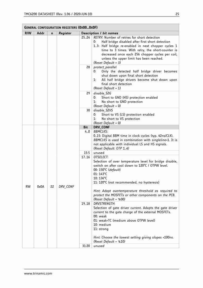
RW 0x0A 22 DRV_CONF
Bit DRV_CONF
4..0 BBMCLKS: 0..15: Digital BBM time in clock cycles (typ. 42ns/CLK). BBMCLKS is used in combination with singleline=1. It is not applicable with individual LS and HS signals. (Reset Default: OTP 1..4)
15:5 unused
17..16 OTSELECT: Selection of over temperature level for bridge disable, switch on after cool down to 120°C / OTPW level. 00: 150°C (default) 01: 143°C 10: 136°C 11: 120°C (not recommended, no hysteresis) Hint: Adapt overtemperature threshold as required to protect the MOSFETs or other components on the PCB. (Reset Default = %00)
19..18 DRVSTRENGTH: Selection of gate driver current. Adapts the gate driver current to the gate charge of the external MOSFETs. 00: weak 01: weak+TC (medium above OTPW level) 10: medium 11: strong Hint: Choose the lowest setting giving slopes <100ns. (Reset Default = %10)
31:20 unused

TMC6200 DATASHEET (Rev. 1.06 / 2020-JUN-10) 26
www.trinamic.com
5.1.1 OTP_READ – OTP configuration memory The OTP memory holds power up defaults for certain registers. All OTP memory bits are cleared to 0 by default. Programming only can set bits, clearing bits is not possible. Factory tuning of the clock frequency affects otp0.0 to otp0.4. The state of these bits therefore may differ between individual ICs.
0X05: OTP_READ – OTP MEMORY MAP
Bit Name Function Comment
7 otp0.7 otp_BBM Reset default for BBM 0: 4 clocks 1: 1 clocks 2: 2 clocks 3: 3 clocks
6 otp0.6
5 otp0.5 otp_S2_LEVEL Reset default for Short detection Levels: 0: S2G_LEVEL = S2VS_LEVEL = 6 1: S2G_LEVEL = S2VS_LEVEL = 12
4 otp0.4 OTP_FCLKTRIM Reset default for FCLKTRIM 0: lowest frequency setting 31: highest frequency setting Attention: This value is pre-programmed by factory clock trimming to the default clock frequency of 24MHz and differs between individual ICs! It should not be altered.
3 otp0.3
2 otp0.2
1 otp0.1
0 otp0.0
TMC6200 DATASHEET (Rev. 1.06 / 2020-JUN-10) 27
www.trinamic.com
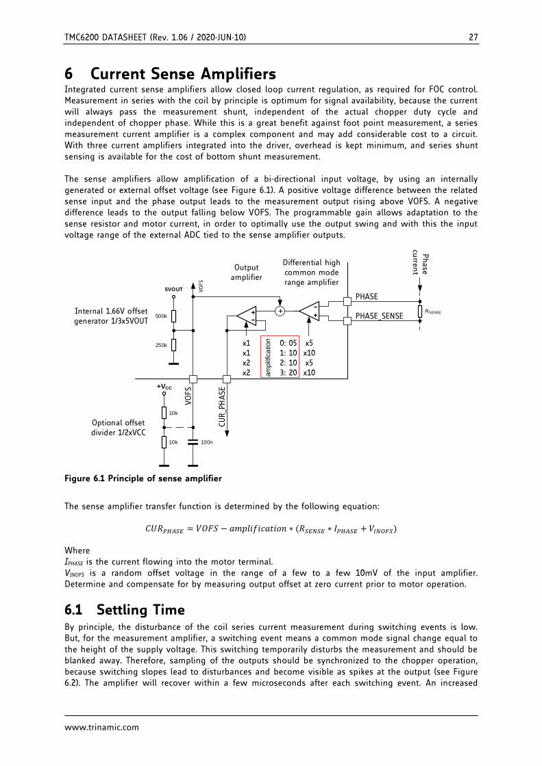
6 Current Sense Amplifiers Integrated current sense amplifiers allow closed loop current regulation, as required for FOC control. Measurement in series with the coil by principle is optimum for signal availability, because the current will always pass the measurement shunt, independent of the actual chopper duty cycle and independent of chopper phase. While this is a great benefit against foot point measurement, a series measurement current amplifier is a complex component and may add considerable cost to a circuit. With three current amplifiers integrated into the driver, overhead is kept minimum, and series shunt sensing is available for the cost of bottom shunt measurement. The sense amplifiers allow amplification of a bi-directional input voltage, by using an internally generated or external offset voltage (see Figure 6.1). A positive voltage difference between the related sense input and the phase output leads to the measurement output rising above VOFS. A negative difference leads to the output falling below VOFS. The programmable gain allows adaptation to the sense resistor and motor current, in order to optimally use the output swing and with this the input voltage range of the external ADC tied to the sense amplifier outputs.
CUR_P
HASE
VOFS
PHASE5VOUT V
OFS
+500k
250k
PHASE_SENSERSENSE
Phase
cu
rrent
Differential high common mode range amplifier
+VCC
Internal 1.66V offset generator 1/3x5VOUT
Optional offset divider 1/2xVCC
10k
10k 100n
x1x1x2x2
Output amplifier
x5x10x5x10
0: 051: 102: 103: 20a
mplifica
tion
Figure 6.1 Principle of sense amplifier
The sense amplifier transfer function is determined by the following equation:
𝐶𝑈𝑅𝑃𝐻𝐴𝑆𝐸 = 𝑉𝑂𝐹𝑆 − 𝑎𝑚𝑝𝑙𝑖𝑓𝑖𝑐𝑎𝑡𝑖𝑜𝑛 ∗ (𝑅𝑆𝐸𝑁𝑆𝐸 ∗ 𝐼𝑃𝐻𝐴𝑆𝐸 + 𝑉𝐼𝑁𝑂𝐹𝑆) Where IPHASE is the current flowing into the motor terminal. VINOFS is a random offset voltage in the range of a few to a few 10mV of the input amplifier. Determine and compensate for by measuring output offset at zero current prior to motor operation.
6.1 Settling Time By principle, the disturbance of the coil series current measurement during switching events is low. But, for the measurement amplifier, a switching event means a common mode signal change equal to the height of the supply voltage. This switching temporarily disturbs the measurement and should be blanked away. Therefore, sampling of the outputs should be synchronized to the chopper operation, because switching slopes lead to disturbances and become visible as spikes at the output (see Figure 6.2). The amplifier will recover within a few microseconds after each switching event. An increased

TMC6200 DATASHEET (Rev. 1.06 / 2020-JUN-10) 28
www.trinamic.com
settling time can result from increased length of motor cables and capacitive load on the cables, or parasitic inductivity of the sense resistors.
Figure 6.2 Amplifier Settling after coil switch event (Green: Coil output, Yellow: Amplifier output)
Figure 6.3 Output correctly sampled with sine wave current and 1.66V offset
Attention Each switching event on one of the motor outputs will cause a spike on the related current measurement amplifier output. Its settling time of roughly 2µs to 4µs (depending on supply voltage and sense resistors) should be blanked away by ignoring the output voltage during this time. This can be ensured, when the external ADC samples the output synchronously with the chopper period.
6.2 Current Amplifier Offset
6.2.1 Initial Offset The amplifiers have a good amplification tolerance, but due to production stray, they show a random offset voltage (see Figure 6.4). Offset voltage especially concerns input offset, as the input offset voltage becomes amplified by the actual amplifications setting, i.e. factor 5, 10 or 20. Therefore, a higher amplification setting means a higher offset voltage and higher offset stray. To compensate for this offset (VINOFS), individually sample the amplifier outputs while the motor driver is disabled and use

TMC6200 DATASHEET (Rev. 1.06 / 2020-JUN-10) 29
www.trinamic.com
the resulting value as zero-reference. When changing amplification in the application, scale the offset measured with a different amplification accordingly.
6.2.2 Thermal Drift Further, the offset has a random certain thermal drift. Figure 6.5 shows an example. Thermal drift especially concerns applications, where the IC heats up significantly during operation. Thermal compensation therefore becomes necessary, when low motor currents have to be exactly measured in a high current application, e.g. for field-oriented motor control. As the thermal drift basically shows a linear dependence on the temperature, taking offset measurements at two temperature values will be sufficient for linear interpolation and extrapolation of the actual offset. Therefore, board temperature near the IC / near the power stage shall be measured. Compensation based on an initial testing phase temperature curve per channel will be sufficient.
Example for offset compensation including thermal drift compensation: 1) Measure and compensate initial value at each power-up of the IC. 2) When the unit is powered up for the first time, store temperature and offset value for each channel 3) When the unit reaches a certain increased temperature for the first time (e.g. +40°C more than at step 2), redo 1) and store temperature and offset values to EEPROM. 4) Use the results of steps 2) and 3) for compensating thermal drift during operation, by interpolating between and extrapolating beyond the stored values
For applications with continuous motor operation, a floating mean value should be sufficient to compensate for amplifier offset.
Figure 6.4 Random Output Offset at 20x amplification (Yellow: Output, Blue: VOFS input)

TMC6200 DATASHEET (Rev. 1.06 / 2020-JUN-10) 30
www.trinamic.com
Figure 6.5 Example for Thermal Offset Drift at output (5x amplification) [mV] from 30°C to 120°C
Attention The current amplifiers show a random offset. It has to be compensated individually for each channel in order to yield the absolute current. An initial compensation (after power-up) will basically eliminate most of this offset. Further, the current amplifiers show a random thermal drift. For applications, which significantly heat up during operation, this thermal effect should be compensated by either of these methods: a) floating AC mean value (AC coupling) b) linearized two-point compensation using stored values and temperature measurement c) repeated compensation after a certain amount of heat up / time (may be stored and used for b)) Measure power stage temperature near the IC to allow for thermal compensation of offset!
Attention When operating in conjunction with the TMC4671 or TMC8670, a compensation of the drift is not possible. Therefore, we recommend using the internal sensing only for applications with low temperature range, and for tiny applications up to 8A, using 5 times amplification of the sense amplifier, which exhibits the lowest relative drift. For higher motor current, use external sense amplifiers.

TMC6200 DATASHEET (Rev. 1.06 / 2020-JUN-10) 31
www.trinamic.com
6.3 Choice of Sense Resistors Choose sense resistors with regard to the maximum motor current desired. Be sure to provide sufficient headroom for your current regulation loop in order to operate the motor at short time peak currents. A regulation loop always needs a headroom of 25% to 50%. The following table shows a choice of standard resistors (partially yielded by paralleling two resistors) and the peak currents which can safely be measured with 1.65V or 2.5V Offset voltage. The choice of amplification is shown as second parameter. An amplification of 20 only can be set when using the SPI interface.
CHOICE OF RSENSE AND AMPLIFICATION DEPENDING ON MAX. COIL CURRENT
RSENSE [mΩ] Amplification factor
Current range [A] RMS motor current limit [A]
Max. power dissipation of RSENSE [W]
150 10 0.7 0.5 0.05
150 5 1.3 1 0.15
100 5 2 1.5 0.23
75 5 2.6 2 0.3
33 10 3 2.2 0.16
25 10 4 3 0.23
50 5 4 3 0.45
33 5 6 4.5 0.67
15 10 6.5 5 0.38
25 5 8 6 0.9
10 10 10 7.5 0.56
5 10 20 15 1.1
2.5 20 20 15 0.56
2.5 10 40 30 2.3
1 20 50 ([email protected] ofs.) 37 1.4
Sense resistors should be carefully selected. The full motor current flows through the sense resistors. Due to chopper operation the sense resistors see pulsed current from the MOSFET bridges. Therefore, a low-inductance type such as film or composition resistors is required to prevent voltage spikes causing ringing on the sense voltage inputs leading to unstable measurement results. Also, a low-inductance, low-resistance PCB layout is essential. Please also refer to layout considerations in chapter 12. With low resistor values, it becomes more critical to do symmetrical and low resistive PCB traces. CALCULATION OF PEAK SENSE RESISTOR POWER DISSIPATION
𝑃𝑅𝑆𝑀𝐴𝑋 = 𝐼𝐶𝑂𝐼𝐿2 ∗ 𝑅𝑆𝐸𝑁𝑆𝐸
Hint For best precision of current measurement, it is advised to measure and fine tune the current in the application. Choose the sense resistors to the next value covering the desired motor peak current.
Attention Be sure to use a symmetrical sense resistor layout for each bridge and short and straight sense resistor traces of identical length. Well matching sense resistors ensure best performance. A compact layout with massive ground plane is best to avoid parasitic resistance effects.

TMC6200 DATASHEET (Rev. 1.06 / 2020-JUN-10) 32
www.trinamic.com
7 Diagnostics and Protection The TMC6200 supplies a complete set of diagnostic and protection capabilities, like short circuit protection and undervoltage detection. See the DRV_STATUS table for details.
7.1 Temperature Sensors The driver integrates a four-level temperature sensor (120°C pre-warning and selectable 136°C / 143°C / 150°C thermal shutdown) for diagnostics and for protection of the IC and the power MOSFETs and adjacent components against excess heat. Choose the overtemperature level to safely cover error conditions like missing heat convection. Heat is mainly generated by the power MOSFETs, and, at increased voltage, by the internal voltage regulators. For many applications, already the overtemperature pre-warning will indicate an abnormal operation situation and can be used to initiate user warning or power reduction measures like motor current reduction. The thermal shutdown is just an emergency measure and temperature rising to the shutdown level should be prevented by design.
After triggering the overtemperature sensor (ot flag), the driver remains switched off until the system temperature falls below the pre-warning level (otpw) to avoid continuous heating to the shutdown level.
7.2 Short Protection The TMC6200 protects the MOSFET power stages against a short circuit or overload condition by monitoring the voltage drop in the high-side MOSFETs, as well as the voltage drop in the low-side MOSFETs (Figure 7.1). A programmable short detection delay (shortdelay) allows adjusting the detector to work with very slow switching slopes. Additionally, the short detector allows filtering of the signal. This helps to prevent spurious triggering caused by effects of PCB layout, or long, adjacent motor cables (SHORTFILTER). All control bits are available via register SHORT_CONF. Additionally, the short detection is protected against single events, e.g. caused by ESD discharges, by retrying up to three times before switching off the motor continuously (program in SHORT_CONF.RETRY).
Parameter Description Setting Comment
S2VS_LEVEL Short or overcurrent detector level for lowside FETs. Checks for voltage drop in LS MOSFET and optional bottom shunt resistor. Hint: May be tuned for sensitive detection.
4…15 1 (highest sensitivity) … 15 (lowest sensitivity) (Reset Default: OTP 6 / 12)
S2G_LEVEL S2G_LEVEL: Short to GND detector level for highside FETs. Checks for voltage drop on high side MOSFET.
2…15 2 (highest sensitivity) … 15 (lowest sensitivity) (Reset Default: OTP 6 / 12)
SHORT_ FILTER
Spike filtering bandwidth for short detection Hint: Increase value, if erroneous short detection occurs.
0…3 0 (lowest, 100ns), 1 (1µs) (Reset Default), 2 (2µs), 3 (3µs)
RETRY Number of retries after short detection until permanent brigde shutdown
0…3 (Reset Default = 3)
shortdelay shortdelay: Short detection delay The delay shall cover the bridge switching time.
0/1 0=750ns: normal, 1=1500ns: high
disable_S2VS 1: Disable short to VS protection. 0/1 Leave detection enabled for normal use (0).
disable_S2G 1: Disable short to GND protection. 0/1 Leave detection enabled for normal use (0).
protectparallel 0: Individual half bridge protection 1: Disable all bridges upon single half bridge short condition
0/1 (Reset Default = 1)

TMC6200 DATASHEET (Rev. 1.06 / 2020-JUN-10) 33
www.trinamic.com
LS short detection(S2VS)
No-short area
HS short detection
(S2G)
No-short area
BMx (coil output
voltage)
Internal high-side driver enable
VS-VBM
S2G level
0V
VS
tSD
detection activeShort to GND monitor phase
Internal Error Flag
tSD
Short detectedshort delay
shortdelay
inactive
Short to GND detected
Driver disable
01
01
Output floating
S2VS levelVBM
Short to VS monitor phaseshort delay
inactivedetection
activeinactive
inactive
tSD
Internal low-side driver enable 0
1
Figure 7.1 Short detection (U, V or W output)
As the low-side short detection includes an optional bottom shunt resistor, it can be set to a high sensitivity and provides good precision of current detection. This way, it will safely cover most overcurrent conditions, i.e. when the motor stalls, or is abruptly stopped in stealthChop mode.
Once a short condition is safely detected, the corresponding driver bridge (U, V or W) becomes switched off, and the corresponding s2gu, s2gv or s2gw flag, respectively s2vsu, s2vsv or s2vsw becomes set. Optionally, the complete bridge becomes switched off (set protect_parallel). To restart the motor, disable and re-enable the driver. Attention: Short protection cannot protect the system and the power stages for all possible short events, as a short event is rather undefined and a complex network of external components may be involved. Therefore, short circuits should basically be avoided.
Hint Fine tune low-side short detection threshold, in order to provide a sensitive overcurrent protection, e.g. to protect motor and power stage. The reproducibility mainly depends on production stray of the MOSFETs and is typically within +-30%. To see any overcurrent pulse at the FAULT output, set flag short_direct. Set a high value for high-side short protection, because detection is more subject to stray and inductive voltage drop on interconnections.

TMC6200 DATASHEET (Rev. 1.06 / 2020-JUN-10) 34
www.trinamic.com
8 External Reset The chip is loaded with default values during power on via its internal power-on reset. In order to reset the chip to power on defaults, any of the supply voltages monitored by internal reset circuitry (VSA, +5VOUT or VCC_IO) must be cycled. As +5VOUT is the output of the internal voltage regulator, it cannot be cycled via an external source except by cycling VSA. It is easiest and safest to cycle VCC_IO in order to completely reset the chip. Also, current consumed from VCC_IO is low and therefore it has simple driving requirements. Due to the input protection diodes not allowing the digital inputs to rise above VCC_IO level, all inputs must be driven low during this reset operation. When this is not possible, an input protection resistor may be used to limit current flowing into the related inputs.
9 Clock Oscillator and Input The clock is the timing reference for the internal BBM time generator and is used to operate the SPI interface. The factory-trimmed on-chip clock oscillator provides timing which is sufficient for most use cases.
9.1 Using the Internal Clock Directly tie the CLK input to GND near to the IC if the internal clock oscillator is to be used. It provides a precision of roughly +-4%, which is precise enough for BBM operation.
9.2 Using an External Clock When an external clock is available, a frequency of 4 MHz to 13.4 MHz is possible (max. 16MHz with 50% dutycycle). Especially with low clock frequency, make sure, that the SPI timing is kept in order to ensure proper SPI operation. Make sure, that the clock source supplies clean CMOS output logic levels and steep slopes when using a high clock frequency. The external clock input is enabled with the second positive polarity seen on the CLK input.
Attention Switching off the external clock frequency prevents the driver from operating normally. Therefore, an internal watchdog switches back to internal clock in case the external signal is missing for more than roughly 32 internal clock cycles.
9.2.1 Considerations on the Frequency A higher frequency allows more precise BBM timing and faster SPI operation. A lower frequency will reduce power consumption of the IC, which especially at high VSA supply voltages reduces overall power consumption by a few 100mW. However, the internal timing should be sufficient for most applications.

TMC6200 DATASHEET (Rev. 1.06 / 2020-JUN-10) 35
www.trinamic.com
10 Absolute Maximum Ratings The maximum ratings may not be exceeded under any circumstances. Operating the circuit at or near more than one maximum rating at a time for extended periods shall be avoided by application design.
Parameter Symbol Min Max Unit
Supply voltage operating with inductive load VVS, VVSA -0.5 65 V
Supply and bridge voltage short time peak (limited by peak voltage on charge pump output and Cxx pins*)
VVSMAX 70 V
VSA supply voltage VVSAMAX -0.5 65 V
Peak voltages on Cxx bootstrap pins and VCP VCxCP 85 V
Supply voltage V12 V12VOUT -0.5 15 V
Peak voltages on U/V/W pins (due to stray inductivity) VX -6 VVS+6 V
Peak voltages on Cxx bootstrap pins relative to BM VCxx -0.5 16 V
I/O supply voltage VVIO -0.5 5.5 V
Supply voltage (5VOUT) V5VOUT -0.5 5.5 V
Logic input voltage VI -0.5 VVIO+0.5 V
Maximum current to / from digital pins and analog low voltage I/Os (short time peak current)
IIO +/-500 mA
Maximum differential input voltage for current amplifier VX-VSENSEX +/-1.5 V
Maximum short time input current for current amplifier ISENSEX +/-200 mA
5V regulator output current (internal plus external load) I5VOUT 30 mA
5V regulator continuous power dissipation (VVSA-5V) * I5VOUT P5VOUT 1 W
12V regulator output current (internal plus external load) I12VOUT 20 mA
12V regulator continuous power dissipation (VVM-5V) * I5VOUT P12VOUT 0.5 W
Junction temperature TJ -50 150 °C
Storage temperature TSTG -55 150 °C
ESD-Protection for interface pins (Human body model, HBM)
VESDAP 4 kV
ESD-Protection for handling (Human body model, HBM) VESD 1 kV
*) Stray inductivity of power routing will lead to ringing of the supply voltage when driving an inductive load. This ringing results from the fast switching slopes of the driver outputs in combination with reverse recovery of the body diodes of the output driver MOSFETs. Even small trace inductivities as well as stray inductivity of sense resistors can easily generate a few volts of ringing leading to temporary voltage overshoot. This should be considered when working near the maximum voltage.
11 Electrical Characteristics
11.1 Operational Range Parameter Symbol Min Max Unit
Junction temperature TJ -40 125 °C
Supply voltage for motor and bridge VVS 10 60 V
Supply voltage VSA VVSA 10 60 V
Supply voltage for VSA and 12OUT (internal gate voltage regulator bridged)
V12VOUT, VVSA
10 13 V
Lower Supply voltage (reduced spec, short to GND protection not functional), lower limit depending on MOSFETs gate threshold voltage and load current
VVS 8 V
I/O supply voltage VVIO 3.00 5.25 V

TMC6200 DATASHEET (Rev. 1.06 / 2020-JUN-10) 36
www.trinamic.com
11.2 DC and Timing Characteristics DC characteristics contain the spread of values guaranteed within the specified supply voltage range unless otherwise specified. Typical values represent the average value of all parts measured at +25°C. Temperature variation also causes stray to some values. A device with typical values will not leave Min/Max range within the full temperature range.
Power Supply Current DC-Characteristics
VVS = VVSA = 24.0V
Parameter Symbol Conditions Min Typ Max Unit
Total supply current, driver disabled IVS + IVSA
IS internal clock 11 15 mA
VSA supply current (VS and VSA separated)
IVSA fCLK=24MHz / internal clock, driver disabled
8 mA
Internal current consumption from 5V supply on VCC pin
IVCC fCLK=24MHz 6 mA
IO supply current (typ. at 5V) IVIO no load on outputs, inputs at VIO or GND Excludes pullup / pull-down resistors
15 30 µA
Motor Driver DC- and Timing-Characteristics
VVS = 24.0V; Tj=50°C
Parameter Symbol Conditions Min Typ Max Unit
RDSON lowside off driver RONL Gate off 1.0 1.6 Ω
RDSON highside off driver RONH Gate off 1.3 2.0 Ω
Gate drive current low side MOSFET turning on at 2V VGS
ISLPON0 DRIVESTRENGTH=0 400 mA
ISLPON2 DRIVESTRENGTH=2 800 mA
ISLPON3 DRIVESTRENGTH=3 1200 mA
Gate drive current high side MOSFET turning on at 2V VGS
ISLPON0 DRIVESTRENGTH=0 400 mA
ISLPON2 DRIVESTRENGTH=2 800 mA
ISLPON3 DRIVESTRENGTH=3 1200 mA
Gate drive current low side MOSFET turning off at 4V VGS
ISLPOFF0 DRIVESTRENGTH=0 600 mA
ISLPOFF2 DRIVESTRENGTH=2 1200 mA
ISLPOFF3 DRIVESTRENGTH=3 1800 mA
Gate drive current high side MOSFET turning on at 4V VGS
ISLPOFF0 DRIVESTRENGTH=0 600 mA
ISLPOFF2 DRIVESTRENGTH=2 1200 mA
ISLPOFFN3 DRIVESTRENGTH=3 1800 mA
Minimum effective BBM time enforced in individual or singleline mode
tBBM0 Individual LS and HS signals (singleline=0)
30 50 70 ns
Reaction delay time LS/HS input signal change to start of gate driver output change
tDLY Individual LS and HS signals (singleline=0)
65 85 110 ns
Matching difference of gate driver reaction delay times
tDLYMATCH Individual LS and HS signals (singleline=0)
10 ns

TMC6200 DATASHEET (Rev. 1.06 / 2020-JUN-10) 37
www.trinamic.com
Charge Pump DC-Characteristics
Parameter Symbol Conditions Min Typ Max Unit
Charge pump output voltage VVCP-VVS operating V12VOUT -2
V12VOUT -1
V
Charge pump voltage threshold for undervoltage detection
VVCP-VVS rising, using internal 5V regulator voltage
4.5 5.5 6.5 V
Charge pump frequency fCP 1/32 fCLKOSC
Linear Regulator DC-Characteristics
VVS = VVSA = 24.0V
Parameter Symbol Conditions Min Typ Max Unit
Output voltage V5VOUT TJ = 25°C 4.80 5.0 5.20 V
Deviation of output voltage over the full temperature range
V5VOUT(DEV) drivers disabled
TJ = full range
+/-5 +/-50 mV
Deviation of output voltage over the supply voltage
V5VOUT(DEV) drivers disabled, internal clock TA = 25°C
VVSA = 10V to 30V
+/-20 mV / 10V
Output voltage V12VOUT operating, internal clock
TJ = 25°C
10.8 11.5 12.2 V
Clock Oscillator and Input Timing-Characteristics
Parameter Symbol Conditions Min Typ Max Unit
Clock oscillator frequency (factory calibrated)
fCLKOSC tJ=-50°C 23.4 MHz
fCLKOSC tJ=50°C 23 24.0 25 MHz
fCLKOSC tJ=150°C 24.2 MHz
External clock frequency (operating)
fCLK 40%..60% dutycycle for typ. 50% for max.
4 10-13.4 16 MHz
External clock high / low level time
tCLKH / tCLKL
CLK driven to 0.1 VVIO / 0.9 VVIO
10 ns
External clock timeout detection in cycles of internal fCLKOSC
tCLKH1 CLK driven high 32 48 cycles fCLKOSC

TMC6200 DATASHEET (Rev. 1.06 / 2020-JUN-10) 38
www.trinamic.com
Short Detection DC-Characteristics
Parameter Symbol Conditions Min Typ Max Unit
Short to GND / Short to VS detector delay (Start of gate switch on to short detected) Including 100ns filtering time
tSD0 FILT_ISENSE=0 S2xx_LEVEL=6 shortdelay=0
0.5 0.85 1.1 µs
tSD1 shortdelay=1 1.1 1.6 2.2 µs
Short detector level S2VS (measurement includes drop in opt. bottom shunt resistor)
VBM S2VS_LEVEL=15 1.4 1.56 1.72 V
S2VS_LEVEL=6 0.55 0.625 0.70 V
Short detector level S2G VS - VBM S2G_LEVEL=15 VS<52V
1.3 1.56 1.85 V
S2G_LEVEL=15 VS<60V
1.0 V
S2G_LEVEL=6 VS<52V
0.46 0.625 0.85 V
S2G_LEVEL=6 VS<60V
0.20 V
Detector Levels DC-Characteristics
Parameter Symbol Conditions Min Typ Max Unit
VVSA undervoltage threshold for RESET
VUV_VSA VVSA rising 3.8 4.2 4.6 V
V5VOUT undervoltage threshold for RESET
VUV_5VOUT V5VOUT rising 3.5 V
VVCC_IO undervoltage threshold for RESET
VUV_VIO VVCC_IO rising (delay typ. 10µs)
2.0 2.2 3.0 V
VVCC_IO undervoltage detector hysteresis
VUV_VIOHYST 0.3 V
Overtemperature prewarning 120°C
TOTPW Temperature rising 100 120 140 °C
Overtemperature shutdown 136 °C
TOT136 Temperature rising 136 °C
Overtemperature shutdown 143 °C
TOT143 Temperature rising 143 °C
Overtemperature shutdown 150 °C
TOT150 Temperature rising 135 150 170 °C

TMC6200 DATASHEET (Rev. 1.06 / 2020-JUN-10) 39
www.trinamic.com
Sense Amplifiers DC-Characteristics
Tj=50°C
Parameter Symbol Conditions Min Typ Max Unit
Duration of Disturbance on sense amplifier output after switching event / settling time
tSETTLING VVS=24V 2 3 µs
VVS=50V
3 4 µs
Amplification AAMPL amplification=0 4.85 5 5.15 V/V
amplification=1 or 2 10 V/V
amplification=3 20 V/V
Current amplifier differential input voltage range with VOFS=2.5V
VDIFF amplification=0 -250 +250 mV
amplification=1 or 2 -150 +150 mV
amplification=3 -75 +75 mV
Current amplifier differential input voltage range with VOFS=1.65V
VDIFF amplification=0 -200 +200 mV
amplification=1 or 2 -100 +100 mV
amplification=3 -40 +40 mV
Amplification absolute tolerance AABSTOL -3 +3 %
Amplification matching between channels
AMATCH Tested at 1/2 full scale
-2 +2 %
Offset voltage variation over sense input voltage (output)
VOFSVAR Vsense=0V to 50V amplification=0
-10 0 +10 mV
Offset voltage variation (input) over temperature *)
VOFSVART -0.25 +-0.1 +0.25 mV/°C
Offset voltage variation (output) over temperature *)
VOFSVART100 25°C to 125°C amplification=0 (5x)
-125 +-50 +125 mV/ 100°C
Current amplifier input voltage range for normal operation
VSENSE, VBM
-1 VVS+1V V
Current amplifier output offset voltage with regard to VOFS
VOFS amplification=0 -130 +130 mV
amplification=1/2 -250 +250 mV
amplification=3 -500 +500 mV
Current amplifier output voltage range
VCUR 0.1 VVOFS
+-1.5 V5VOUT -0.1
V
VOFS input voltage range VVOFS 1.5 1.65V or 2.5V
2.7 V
Sense amplifier output resistance RCUR 36 56 76 Ω
Sense amplifier output current ICUR Swing 250mV to V5VOUT-500mV
-1 +1 mA
Input Resistance VOFS pin RVOFS 130 165 210 kΩ
Output voltage with VOFS open VVOFS V5VOUT/3 V
*) Parameter characterized by sampling, only

TMC6200 DATASHEET (Rev. 1.06 / 2020-JUN-10) 40
www.trinamic.com
Digital pins DC-Characteristics
Parameter Symbol Conditions Min Typ Max Unit
Input voltage low level VINLO -0.3 0.3 VVIO V
Input voltage high level VINHI 0.7 VVIO VVIO+0.3 V
Input Schmitt trigger hysteresis VINHYST 0.12 VVIO
V
Output voltage low level VOUTLO IOUTLO = 2mA 0.2 V
Output voltage high level VOUTHI IOUTHI = -2mA VVIO-0.2 V
Input leakage current IILEAK -10 10 µA
Pullup / pull-down resistors RPU/RPD 132 166 200 kΩ
Digital pin capacitance C 3.5 pF
11.3 Thermal Characteristics The following table shall give an idea on the thermal resistance of the package. The thermal resistance for a four-layer board will provide a good idea on a typical application. Actual thermal characteristics will depend on the PCB layout, PCB type and PCB size. The thermal resistance will benefit from thicker CU (inner) layers for spreading heat horizontally within the PCB. Also, air flow will reduce thermal resistance.
Parameter Symbol Conditions Typ Unit
Typical power dissipation PD 20kHz chopper, 24V supply, internal supply regulators
<0.5 W
Thermal resistance junction to ambient on a multilayer board
RTMJA Dual signal and two internal power plane board (2s2p) as defined in JEDEC EIA JESD51-5 and JESD51-7 (FR4, 35µm CU, 70mm x 133mm, d=1.5mm)
21 K/W
Thermal resistance junction to board
RTJB PCB temperature measured within 1mm distance to the package leads
8 K/W
Thermal resistance junction to case
RTJC Junction temperature to heat slug of package
3 K/W
Table 11.1 Thermal characteristics TQFP48-EP
The thermal resistance in an actual layout can be tested by checking for the heat up caused by the standby power consumption of the chip. When no motor is attached, all power seen on the power supply is dissipated within the chip.

TMC6200 DATASHEET (Rev. 1.06 / 2020-JUN-10) 41
www.trinamic.com
12 Layout Considerations
12.1 Exposed Die Pad The TMC6200 uses its die attach pad to dissipate heat from the gate drivers and the linear regulator to the board. For best electrical and thermal performance, use a reasonable amount of solid, thermally conducting vias between the die attach pad and the ground plane. The printed circuit board should have a solid ground plane spreading heat into the board and providing for a stable GND reference.
12.2 Wiring GND All signals of the TMC6200 are referenced to their respective GND. Directly connect all GND pins under the device to a common ground area (GND, GNDP, GNDA and die attach pad). The GND plane right below the die attach pad should be treated as a virtual star point. For thermal reasons, the PCB top layer shall be connected to a large PCB GND plane spreading heat within the PCB.
Attention Place the TMC6200 near to the MOSFET bridge in order to avoid ringing leading to GND differences.
12.3 Wiring Bridge Supply The power bridge will draw the full coil current in pulses with extremely high dI/dt. Thus, any inductivity between VS supply filtering and the MOSFETs can lead to severe voltage spikes. This has to be avoided. Avoid any bend in the supply traces between filtering capacitors and MOSFET switches, and keep distance as small as possible. Especially for high current, use a separate plane for the supply voltage, and a sufficient number and capacity for supply filtering. Use an additional capacitor for the IC VS pin, as additional ripple voltage would cause severe current spikes on the charge pump capacitor. A tiny series resistor can be added to avoid this.
Attention Keep supply voltage ripple low, by using sufficient filtering capacity close to the MOSFET bridge.
12.4 Supply Filtering The 5VOUT output voltage ceramic filtering capacitor (2.2 to 4.7 µF recommended) should be placed as close as possible to the 5VOUT pin, with its GND return going directly to the GNDA pin. This ground connection shall not be shared with other loads or additional vias to the GND plane. Use as short and as thick connections as possible. A 100 nF or larger filtering capacitor should be placed as closely as possible to the VSA pin to ground plane. Provide sufficient filtering capacity near the power bridge MOSFETs, in order to avoid ringing following each switching event. Make sure, that VS does not see excessive voltage spikes caused by bridge operation and place a 100 nF or larger filter capacitor to GND close to the VS pin.
Please carefully read chapters 3.4 and 3.5 to understand the special considerations with regard to layout and component selection for the external MOSFET power bridges.

TMC6200 DATASHEET (Rev. 1.06 / 2020-JUN-10) 42
www.trinamic.com
12.5 Layout Example Schematic extract of TMC6200-EVAL (TMC6200+MOSFETs shown)
1- Top Layer (assembly side)
2- Inner Layer (GND)

TMC6200 DATASHEET (Rev. 1.06 / 2020-JUN-10) 43
www.trinamic.com
3- Inner Layer (supply VS)
4- Bottom Layer
Components
Figure 12.1 Layout example
Please refer www.trinamic.com for complete schematic and layout data of the evaluation board.

TMC6200 DATASHEET (Rev. 1.06 / 2020-JUN-10) 44
www.trinamic.com
13 Package Mechanical Data
13.1 Dimensional Drawings TQFP48-EP Attention: Drawings not to scale.
Figure 13.1 Dimensional drawings TQFP48-EP

TMC6200 DATASHEET (Rev. 1.06 / 2020-JUN-10) 45
www.trinamic.com
Parameter Ref Min Nom Max
total thickness A - - 1.2
stand off A1 0.05 - 0.15
mold thickness A2 0.95 1 1.05
lead width (plating) b 0.17 0.22 0.27
lead width b1 0.17 0.2 0.23
lead frame thickness (plating)
c 0.09 - 0.2
lead frame thickness c1 0.09 - 0.16
body size X (over pins) D 9.0
body size Y (over pins) E 9.0
body size X D1 7.0
body size Y E1 7.0
lead pitch e 0.5
lead L 0.45 0.6 0.75
footprint L1 1 REF
0° 3.5° 7°
1 0° - -
2 11° 12° 13°
3 11° 12° 13°
R1 0.08 - -
R2 0.08 - 0.2
S 0.2 - -
exposed die pad size X M 4.9 5 5.1
exposed die pad size Y N 4.9 5 5.1
package edge tolerance aaa 0.2
lead edge tolerance bbb 0.2
coplanarity ccc 0.08
lead offset ddd 0.08
mold flatness eee 0.05
13.2 Package Codes
Type Package Temperature range Code & marking MSL level
TMC6200-TA TQFP-EP48 (RoHS) -40°C ... +125°C TMC6200-TA MSL 3 / 160h
TMC6200-TA-T Tape on reel packed products

TMC6200 DATASHEET (Rev. 1.06 / 2020-JUN-10) 46
www.trinamic.com
14 Disclaimer TRINAMIC Motion Control GmbH & Co. KG does not authorize or warrant any of its products for use in life support systems, without the specific written consent of TRINAMIC Motion Control GmbH & Co. KG. Life support systems are equipment intended to support or sustain life, and whose failure to perform, when properly used in accordance with instructions provided, can be reasonably expected to result in personal injury or death. Information given in this data sheet is believed to be accurate and reliable. However no responsibility is assumed for the consequences of its use nor for any infringement of patents or other rights of third parties which may result from its use. Specifications are subject to change without notice. All trademarks used are property of their respective owners.
15 ESD Sensitive Device The TMC6200 is an ESD sensitive CMOS device sensitive to electrostatic discharge. Take special care to use adequate grounding of personnel and machines in manual handling. After soldering the devices to the board, ESD requirements are more relaxed. Failure to do so can result in defect or decreased reliability.
16 Designed for Sustainability Sustainable growth is one of the most important and urgent challenges today. We at Trinamic try to contribute by designing highly efficient IC products, to minimize energy consumption, ensure best customer experience and long-term satisfaction by smooth and silent run, while minimizing the demand for external resources, e.g. for power supply, cooling infrastructure, reduced motor size and magnet material by intelligent control interfaces and advanced algorithms.
Please help and design efficient and durable products made for a sustainable world.

TMC6200 DATASHEET (Rev. 1.06 / 2020-JUN-10) 47
www.trinamic.com
17 Table of Figures FIGURE 1.1 STANDALONE APPLICATION USING DIFFERENTIAL SENSING ....................................................................................... 4 FIGURE 1.2 STANDALONE APPLICATION USING SINGLE SHUNT CURRENT SENSING ....................................................................... 5 FIGURE 1.3 SPI MODE CONFIGURATION ...................................................................................................................................... 5 FIGURE 2.1 TMC6200-TA PINNING TQFP-EP 48 (7X7MM² BODY, 9X9MM² WITH LEADS) ........................................................ 7 FIGURE 3.1 STANDARD APPLICATION CIRCUIT ........................................................................................................................... 10 FIGURE 3.2 EXTERNAL GATE VOLTAGE SUPPLY ........................................................................................................................... 11 FIGURE 3.3 STANDBY SWITCH .................................................................................................................................................. 12 FIGURE 3.4 MILLER CHARGE DETERMINES SWITCHING SLOPE .................................................................................................... 13 FIGURE 3.5 SLOPES, MILLER PLATEAU AND BLANK TIME (BMX=U V OR W OUTPUT) ................................................................ 14 FIGURE 3.6 BRIDGE PROTECTION OPTIONS FOR POWER ROUTING INDUCTIVITY ......................................................................... 15 FIGURE 3.7 RINGING OF OUTPUT (GREEN) AND GATE VOLTAGES (YELLOW, BLUE) WITH DRVSTRENGTH=0 ............................ 16 FIGURE 3.8 RINGING OF OUTPUT (GREEN) AND GATE VOLTAGES (YELLOW, BLUE) WITH DRVSTRENGTH=2 ............................ 16 FIGURE 3.9 RINGING OF OUTPUT (GREEN) AND GATE VOLTAGES (YELLOW, BLUE) WITH DRVSTRENGTH=3 ............................ 16 FIGURE 3.10 DIODES FOR SAFE OFF CONDITION WITH HIGH GATE SERIES RESISTANCE ............................................................ 17 FIGURE 4.1 SPI TIMING ............................................................................................................................................................ 20 FIGURE 6.1 PRINCIPLE OF SENSE AMPLIFIER ............................................................................................................................. 27 FIGURE 6.2 AMPLIFIER SETTLING AFTER COIL SWITCH EVENT (GREEN: COIL OUTPUT, YELLOW: AMPLIFIER OUTPUT) ................ 28 FIGURE 6.3 OUTPUT CORRECTLY SAMPLED WITH SINE WAVE CURRENT AND 1.66V OFFSET ....................................................... 28 FIGURE 6.4 RANDOM OUTPUT OFFSET AT 20X AMPLIFICATION (YELLOW: OUTPUT, BLUE: VOFS INPUT) ................................. 29 FIGURE 6.5 EXAMPLE FOR THERMAL OFFSET DRIFT AT OUTPUT (5X AMPLIFICATION) [MV] FROM 30°C TO 120°C................... 30 FIGURE 7.1 SHORT DETECTION (U, V OR W OUTPUT) ............................................................................................................... 33 FIGURE 12.1 LAYOUT EXAMPLE ................................................................................................................................................. 43 FIGURE 13.1 DIMENSIONAL DRAWINGS TQFP48-EP ............................................................................................................... 44
18 Revision History Version Date Author
BD= Bernhard Dwersteg
Description
V0.05 2018-APR-22 BD First version of datasheet based on datasheet TMC6200 V1.0
V0.1 2018-APR-30 BD First complete version based on preliminary data
V0.11 2018-MAY-09 BD Offset voltage added to description, added Eval board schematics
V0.12 2018-MAY-29 BD Minor changes
V0.13 2018-SEP-11 BD P12VOUT Mnemonic in abs. max. table, tables back to 0.25pt lines
V1.00 2018-OKT-30 BD Adapted electrical characteristics
V1.01 2018-NOV-15 BD Reworked schematic showing additional protection components, added chapter on wiring bridge supply
V1.02 2019-JAN-31 BD Characterized and documented thermal drift of sense amplifier offset, added chapter 6.2, re-specification for external clock
V1.03 2019-FEB-13 BD Added example for offset compensation. Added Standby example
V1.04 2019-AUG-08 BD Added ordering codes, changed block diagram
V1.05 2019-NOV-12 BD Minor changes
V1.06 2020-JUN-10 BD Updated logo
Table 18.1 Document Revisions