Embed Size (px)
Citation preview

POWER DRIVER FOR STEPPER MOTORS INTEGRATED CIRCUITS
TRINAMIC Motion Control GmbH & Co. KG Hamburg, Germany
DRIVER 1
DRIVER 2
TMC2041
Protection& Diagnostics
256 µStepSequencer
256 µStepSequencer
Protection& Diagnostics
Step/Dir
Step/Dir
SPI
Power Supply
Charge Pump
Motor 2
stallGuard2 coolStep
Motor 1
UART / SPI configuration&
diagnosticsUART
Enable
TMC2041 DATASHEET
BLOCK DIAGRAM
FEATURES AND BENEFITS
Two 2-phase stepper motors
Drive Capability up to 2x 1.1A coil current (2x 1.5A peak)
Parallel Option for one motor at 2.2A (3A peak)
Voltage Range 4.75… 26V DC
SPI & Single Wire UART for configuration and diagnostics
Highest Resolution up to 256 microsteps per full step
microPlyer™ microstep interpolation
spreadCycle™ highly dynamic motor control chopper
stallGuard2™ high precision sensorless motor load detection
coolStep™ current control for energy savings up to 75%
Full Protection & Diagnostics
Compact Size 7x7mm2 QFN48 package
APPLICATIONS
Office Automation Antenna Positioning 3D printers Battery powered applications Printer and Scanner Pumps and Valves Medical Applications Office and Laboratory equipment
DESCRIPTION
The TMC2041 is a compact, dual stepper motor driver IC with serial interfaces for configuration and diagnostics. It is pin compatible to the fully featured TMC5041 and TMC5072 drivers with internal mo-tion controller. The TMC2041 is intended for all applications, where an internal motion controller is not desired, and ramping is done in a microcontroller. Based on TRINAMICs high-performance spreadCycle chopper, the driver allows precise and smooth motor operation. It offers coolStep for energy savings and stallGuard for sensorless stall detection. The complete set of protection and diagnostic functionality ensures reliable operation. High integration, high energy efficiency and a small form factor enable miniaturized and scalable systems for cost effective solutions.
Dual step/direction driver for up to two 2-phase bipolar stepper motors. stallGuard for sensorless homing. SPI, UART (single wire) Configuration and Diagnostics Interface.

TMC2041 DATASHEET (Rev. 1.02 / 2017-MAY-16) 2
www.trinamic.com
Layout for Evaluation
M
M
STEP/DIR FOR UP TO TWO STEPPER MOTORS
CPU TMC2041High-Level Interface
SPI or UART
Step/Dir
Step/Dir
M
STEP/DIR FOR UP TO TWO STEPPER MOTORS
CPU TMC2041High-Level Interface
SPI or UART
Step/Dir
APPLICATION EXAMPLES: HIGH FLEXIBILITY – MULTIPURPOSE USE
The TMC2041 scores with power density and sensorless homing. It features serial interfaces for advanced monitoring and configuration options. The small form factor keeps costs down and allows for miniaturized layouts. Extensive support at the chip, board, and software levels enables rapid design cycles and fast time-to-market with competitive products. High energy efficiency and reliability deliver cost savings in related systems such as power supplies and cooling.
ORDER CODES
Order code Description Size [mm2]
TMC2041-LA Dual axis step/dir driver, QFN-48 7 x 7
TMC2041-EVAL Evaluation board for TMC2041 85 x 55
STARTRAMPE Baseboard for TMC2041-EVAL and further evaluation boards 85 x 55
ESELSBRÜCKE Connector board for plug-in evaluation board system 61 x 38
TMC2041-EVAL EVALUATION BOARD EVALUATION & DEVELOPMENT PLATFORM
The TMC2041-EVAL is part of TRINAMICs universal evaluation board system which provides a convenient handling of the hardware as well as a user-friendly software tool for evaluation. The TMC2041 evaluation board system consists of three parts: STARTRAMPE (base board), ESELSBRÜCKE (connector board including several test points), and TMC2041-EVAL.
The stepper motor driver outputs are switched in parallel. This way, up to 2.2A RMS motors can be driven.
In this application, a single CPU controls two motors using a Step and Direction interface per motor. It initially configures the drivers by programming current settings and chopper, and run and hold current using either the 4 wire SPI interface, or the single wire UART interface. During operation the interface allows access to status information like stallGuard sensorless load measurement.

TMC2041 DATASHEET (Rev. 1.02 / 2017-MAY-16) 3
www.trinamic.com
TABLE OF CONTENTS
1 PRINCIPLES OF OPERATION 4
1.1 KEY CONCEPTS 4 1.2 CONTROL INTERFACES 4 1.3 MOVING AND CONTROLLING THE MOTOR 5 1.4 STALLGUARD2 – MECHANICAL LOAD SENSING 5 1.5 COOLSTEP – LOAD ADAPTIVE CURRENT CONTROL 5
2 PIN ASSIGNMENTS 7
2.1 PACKAGE OUTLINE 7 2.2 SIGNAL DESCRIPTIONS 7
3 SAMPLE CIRCUITS 10
3.1 STANDARD APPLICATION CIRCUIT 10 3.2 5 V ONLY SUPPLY 11 3.3 ONE MOTOR WITH HIGH CURRENT 12 3.4 EXTERNAL 5V POWER SUPPLY 12 3.5 OPTIMIZING ANALOG PRECISION 13 3.6 DRIVER PROTECTION AND EME CIRCUITRY 13
4 SPI INTERFACE 15
4.1 SPI DATAGRAM STRUCTURE 15 4.2 SPI SIGNALS 16 4.3 TIMING 17
5 UART SINGLE WIRE INTERFACE 18
5.1 DATAGRAM STRUCTURE 18 5.2 CRC CALCULATION 20 5.3 UART SIGNALS 20 5.4 ADDRESSING MULTIPLE SLAVES 21
6 REGISTER MAPPING 23
6.1 GENERAL CONFIGURATION REGISTERS 24 6.2 CURRENT SETTING 26 6.3 MOTOR DRIVER REGISTERS 27
7 CURRENT SETTING 32
7.1 SENSE RESISTORS 33
8 SPREADCYCLE AND CLASSIC CHOPPER 34
8.1 SPREADCYCLE CHOPPER 35 8.2 CLASSIC CONSTANT OFF TIME CHOPPER 38 8.3 RANDOM OFF TIME 39
9 DRIVER DIAGNOSTIC FLAGS 40
9.1 TEMPERATURE MEASUREMENT 40 9.2 SHORT TO GND PROTECTION 40 9.3 OPEN LOAD DIAGNOSTICS 40
10 STALLGUARD2 LOAD MEASUREMENT 41
10.1 TUNING STALLGUARD2 THRESHOLD SGT 42 10.2 STALLGUARD2 UPDATE RATE AND FILTER 44
10.3 DETECTING A MOTOR STALL 44 10.4 HOMING WITH STALLGUARD 44 10.5 LIMITS OF STALLGUARD2 OPERATION 44
11 COOLSTEP OPERATION 45
11.1 USER BENEFITS 45 11.2 SETTING UP FOR COOLSTEP 45 11.3 TUNING COOLSTEP 47
12 STEP/DIR INTERFACE 48
12.1 TIMING 48 12.2 CHANGING RESOLUTION 49 12.3 MICROPLYER STEP INTERPOLATOR AND STAND
STILL DETECTION 49
13 QUICK CONFIGURATION GUIDE 51
14 GETTING STARTED 53
14.1 INITIALIZATION EXAMPLES 53
15 EXTERNAL RESET 54
16 CLOCK OSCILLATOR AND CLOCK INPUT 54
16.1 USING THE INTERNAL CLOCK 54 16.2 USING AN EXTERNAL CLOCK 54 16.3 CONSIDERATIONS ON THE FREQUENCY 54
17 ABSOLUTE MAXIMUM RATINGS 55
18 ELECTRICAL CHARACTERISTICS 55
18.1 OPERATIONAL RANGE 55 18.2 DC CHARACTERISTICS AND TIMING
CHARACTERISTICS 56 18.3 THERMAL CHARACTERISTICS 59
19 LAYOUT CONSIDERATIONS 60
19.1 EXPOSED DIE PAD 60 19.2 WIRING GND 60 19.3 SUPPLY FILTERING 60 19.4 SINGLE DRIVER CONNECTION 60 19.5 LAYOUT EXAMPLE 61
20 PACKAGE MECHANICAL DATA 62
20.1 DIMENSIONAL DRAWINGS 62 20.2 PACKAGE CODES 62
21 DISCLAIMER 63
22 ESD SENSITIVE DEVICE 63
23 TABLE OF FIGURES 64
24 REVISION HISTORY 65
25 REFERENCES 65
TMC2041 DATASHEET (Rev. 1.02 / 2017-MAY-16) 4
www.trinamic.com
1 Principles of Operation
VCC_IO
TMC2041
SPI interface
CSN/IO0
SCK/IO1
SDO
SDI/IO2
Step/Dir interface
STE
P1
DIR
1
Step/Dir interface
Sequencer & Microplyer
Single wire interface
5V Voltage regulator
charge pumpVCP
22n
100n
SWION
SW_SEL
CLK_IN
STEP
2
DIR
2
SWIOP
+VM
5VOUT
VSA
4.7µ
+VIO
NEXTADDR
DRV_EN
N
DRV_E
NN
GNDP
GND
GNDA
TST_M
ODE
DIE P
AD
VCC
opt. ext. clock12-16MHz
3.3V or 5VI/O voltage
100n
100nSequencer & Microplyer
Full Bridge A
Full Bridge B
+VM
VS
steppermotor #1
NS
O1A1
O1A2
BR1A
O1B1
O1B2
Driver 1
100n
BR1B
Full Bridge A
Full Bridge B
steppermotor #2
NS
O2A1
O2A2
BR2A
O2B1
O2B2
Driver 2
BR2B
VS
100n
+VM
100µF
CPI
CPO
+VIO
Optional use lower
voltage down to 6V
2R2
470n
R1A
R1B
R2A
R2B
Figure 1.1 Basic application and block diagram
The TMC2041 driver chip is a highly integrated step & direction stepper driver for two stepper motors. The driver, chopper logic, and a 256 microstep sequencer are integrated into the TMC2041. It is pin compatible to the TMC5041 and TMC5072, which provide internal ramping. The TMC2041 offers a number of unique enhancements over similar products. It features automatic standstill current reduction and coolStep for enhanced motor efficiency and provides stallGuard2 for sensorless homing.
1.1 Key Concepts The TMC2041 implements several advanced features which are exclusive to TRINAMIC products. These features contribute toward greater precision, greater energy efficiency, higher reliability, smoother motion, and cooler operation in many stepper motor applications. spreadCycle™ High-precision chopper algorithm available as an alternative to the traditional
constant off-time algorithm.
stallGuard2™ High-precision load measurement using the back EMF on the motor coils.
coolStep™ Load-adaptive current control which reduces energy consumption by as much as 75%.
In addition to these performance enhancements, TRINAMIC motor drivers offer safeguards to detect and protect against shorted outputs, output open-circuit, overtemperature, and undervoltage conditions for enhancing safety and recovery from equipment malfunctions.
1.2 Control Interfaces The TMC2041 supports both, an SPI and a UART based single wire interface with CRC checking. Selection of the actual interface is done via the configuration pin SW_SEL, which can be hardwired to GND or VCC_IO depending on the desired interface. From a software point of view the TMC2041 is a peripheral with a number of control and status registers. Most of them can either be written only or
TMC2041 DATASHEET (Rev. 1.02 / 2017-MAY-16) 5
www.trinamic.com
read only. Some of the registers allow both read and write access. In case read-modify-write access is desired for a write only register, a shadow register can be realized in master software.
1.2.1 SPI Interface The SPI interface is a bit-serial interface synchronous to a bus clock. For every bit sent from the bus master to the bus slave another bit is sent simultaneously from the slave to the master. Communication between an SPI master and the TMC2041 slave always consists of sending one 40-bit command word and receiving one 40-bit status word. The SPI command rate typically is a few commands per complete motor motion.
1.2.2 UART Interface The single wire interface allows differential operation similar to RS485 (using SWIOP and SWION) or single wire interfacing (leaving open SWION). It can be driven by any standard UART. No baud rate configuration is required. An optional ring mode allows chaining of slaves to optimize interfacing for applications with regularly distributed drives.
1.3 Moving and Controlling the Motor 1.3.1 STEP/DIR Interface Each motor is controlled by a step and direction input. Active edges on the STEP input can be rising edges or both rising and falling edges as controlled by another mode bit (DEDGE). Using both edges cuts the toggle rate of the STEP signal in half, which is useful for communication over slow interfaces such as optically isolated interfaces. On each active edge, the state sampled from the DIR input determines whether to step forward or back. Each step can be a fullstep or a microstep, in which there are 2, 4, 8, 16, 32, 64, 128, or 256 microsteps per fullstep. During microstepping, a step impulse with a low state on DIR increases the microstep counter and a high decreases the counter by an amount controlled by the microstep resolution. An internal table translates the counter value into the sine and cosine values which control the motor current for microstepping.
1.4 stallGuard2 – Mechanical Load Sensing stallGuard2 provides an accurate measurement of the load on the motor. It can be used for stall detection as well as other uses at loads below those which stall the motor, such as coolStep load-adaptive current reduction. This gives more information on the drive allowing functions like sensorless homing and diagnostics of the drive mechanics.
1.5 coolStep – Load Adaptive Current Control coolStep drives the motor at the optimum current. It uses the stallGuard2 load measurement information to adjust the motor current to the minimum amount required in the actual load situation. This saves energy and keeps the components cool.
Benefits are:
- Energy efficiency power consumption decreased up to 75%
- Motor generates less heat improved mechanical precision
- Less or no cooling improved reliability
- Use of smaller motor less torque reserve required → cheaper motor does the job Figure 1.2 shows the efficiency gain of a 42mm stepper motor when using coolStep compared to standard operation with 50% of torque reserve. coolStep is enabled above 60RPM in the example.

TMC2041 DATASHEET (Rev. 1.02 / 2017-MAY-16) 6
www.trinamic.com
0
0,1
0,2
0,3
0,4
0,5
0,6
0,7
0,8
0,9
0 50 100 150 200 250 300 350
Efficiency
Velocity [RPM]
Efficiency with coolStep
Efficiency with 50% torque reserve
Figure 1.2 Energy efficiency with coolStep (example)

TMC2041 DATASHEET (Rev. 1.02 / 2017-MAY-16) 7
www.trinamic.com
2 Pin Assignments
2.1 Package Outline
TMC 2041-LAQFN48 7mm x 7mm
0.5 pitch
STEP1
CPO
GNDP
TST_
MODE
O1A
1
VS
O1B
1
BR1A
O1A
2
VS
O1B
2VCC_IO
GND
O2A
2
BR2A
BR2BVS
O2B
2
VS
O2B
1
1GND
SDO
SWIOP
GND
SDI
SCK
CSN
DIR1
STEP2
VSA
GNDA
GND
CPI
CLK
SWION
GNDP
DIR2
BR1B
O2A
1
2
3
4
5
6
7
8
9
10
11
14 15 16 17 18 19 20 21 22 23 24
36
35
34
33
32
31
30
29
28
27
26
48 47 46 45 44 43 42 41 40 39 38DRV_ENN
VCP
37
25
-13
12
-
SWSEL
-
VCC
NEX
TADDR
5VOUT
Figure 2.1 TMC2041 pin assignments.
2.2 Signal Descriptions
Pin Number Type Function
GND 6, 34 GND Digital ground pin for IO pins and digital circuitry.
VCC_IO 7 3.3V or 5V I/O supply voltage pin for all digital pins.
VSA 30 Analog supply voltage for 5V regulator – typically supplied with driver supply voltage. An additional 100nF capacitor to GND (GND plane) is recommended for best performance.
GNDA 31 GND Analog GND. Tie to GND plane.
5VOUT 32 Output of internal 5V regulator. Attach 2.2µF or larger ceramic capacitor to GNDA near to pin for best performance. Use to supply VCC of chip.

TMC2041 DATASHEET (Rev. 1.02 / 2017-MAY-16) 8
www.trinamic.com
Pin Number Type Function
VCC 33 5V supply input for digital circuitry within chip and charge pump. Attach 470nF capacitor to GND (GND plane). Typically supplied by 5VOUT. A 2.2Ω resistor is recommended for decoupling noise from 5VOUT. When using an external supply, make sure, that VCC comes up before or in parallel to 5VOUT or VCC_IO, whichever comes up later!
DIE_PAD - GND Connect the exposed die pad to a GND plane. Provide as many as possible vias for heat transfer to GND plane.
Table 2.1 Low voltage digital and analog power supply pins
Pin Number Type Function
CPO 35 O(VCC) Charge pump driver output. Outputs 5V (GND to VCC) square wave with 1/16 of internal oscillator frequency.
CPI 36 I(VCP) Charge pump capacitor input: Provide external 22nF or 33nF / 50 V capacitor to CPO.
VCP 37 Output of charge pump. Provide external 100nF capacitor to VS.
Table 2.2 Charge pump pins
Pin Number Type Function
GND 1 I unused input, tie to GND
GND 2 I unused input, tie to GND
CSN/IO0 3 I/O Chip select input of SPI interface, programmable IO in UART mode
SCK/IO1 4 I/O Serial clock input of SPI interface, programmable IO in UART mode
SDI/IO2 5 I/O Data input of SPI interface, programmable IO in UART mode
SDO 8 I/O Data output of SPI interface (Tristate, enabled with CSN=0), mode configuration input in UART mode (0 = Normal mode, 1 = Single wire ring mode – SWIO_P is input, SWIO_N is output)
SWIOP 9 I/O Single wire I/O (positive). Serial input in ring mode. Multi-purpose input in SPI mode or encoder 1 N input.
SWION 10 I/O Single wire I/O (negative) for differential mode. Leave open in non-differential mode when operating at 5V IO voltage or tie to desired threshold voltage. Serial output in ring mode. Multi-purpose input in SPI mode or encoder 2 N input.
CLK 11 I Clock input. Tie to GND using short wire for internal clock or supply external clock. The first high signal disables the internal oscillator until power down.
SWSEL 12 I Interface selection input. Tie to GND for SPI mode, tie to VCC_IO for single wire (UART) interface mode.
NEXTADDR 24 I Address increment (if tied high) for single wire (UART) mode. General purpose input in SPI mode
DIR2 25 I Right reference switch input for motor 2, optional DIR input for STEP/DIR operation of motor 2 or encoder 2 B input
STEP2 26 I Left reference switch input for motor 2, optional STEP input for STEP/DIR operation of motor 2
DIR1 27 I Right reference switch input for motor 1, optional DIR input for STEP/DIR operation of motor 1 or encoder 2 A input
STEP1 28 I Left reference switch input for motor 1, optional STEP input for STEP/DIR operation of motor 1
DRV_ENN 29 I Enable input for motor drivers. The power stage becomes switched off (all motor outputs floating) when this pin becomes driven to a high level. Tie to GND for normal operation.
TST_MODE 48 I Test mode input. Tie to GND using short wire.
- 13, 23, 38 N.C. Unused pins – no internal electrical connection. Leave open or tie to GND for compatibility with future devices.
Table 2.3 Digital I/O pins (all related to VCC_IO supply)

TMC2041 DATASHEET (Rev. 1.02 / 2017-MAY-16) 9
www.trinamic.com
Pin Number Type Function
O2A1 14 O (VS) Motor 2 coil A output 1
BR2A 15 Sense resistor connection for motor 2 coil A. Place sense resistor to GND near pin.
O2A2 16 O (VS) Motor 2 coil A output 2
VS 17, 19 Motor supply voltage. Provide filtering capacity near pin with shortest loop to nearest GNDP pin (respectively via GND plane).
GNDP 18 GND Power GND. Connect to GND plane near pin.
O2B1 20 O (VS) Motor 2 coil B output 1
BR2B 21 Sense resistor connection for motor 2 coil B. Place sense resistor to GND near pin.
O2B2 22 O (VS) Motor 2 coil B output 2
O1B2 39 O (VS) Motor 1 coil B output 2
BR1B 40 Sense resistor connection for motor 1 coil B. Place sense resistor to GND near pin.
O1B1 41 O (VS) Motor 1 coil B output 1
VS 42, 44 Motor supply voltage. Provide filtering capacity near pin with shortest loop to nearest GNDP pin (respectively via GND plane).
GNDP 43 GND Power GND. Connect to GND plane near pin.
O1A2 45 O (VS) Motor 1 coil A output 2
BR1A 46 Sense resistor connection for motor 1 coil A. Place sense resistor to GND near pin.
O1A1 47 O (VS) Motor 1 coil A output 1
Table 2.4 Power driver pins

TMC2041 DATASHEET (Rev. 1.02 / 2017-MAY-16) 10
www.trinamic.com
3 Sample Circuits The sample circuits show the connection of the external components in different operation and supply modes. The connection of the bus interface and further digital signals is left out for clarity.
3.1 Standard Application Circuit
VCC_IO
TMC2041
SPI interface
CSN/IO0
SCK/IO1
SDO
SDI/IO2
Step/Dir interface
STE
P1
DIR
1
Step/Dir interface
Sequencer & Microplyer
Single wire interface
5V Voltage regulator
charge pumpVCP
22n
100n
SWION
SW_SEL
CLK_IN
STEP
2
DIR
2SWIOP
+VM
5VOUT
VSA
4.7µ
+VIO
NEXTADDR
DRV_EN
N
DRV_E
NN
GNDP
GND
GNDA
TST_M
ODE
DIE P
AD
VCC
opt. ext. clock12-16MHz
3.3V or 5VI/O voltage
100n
100nSequencer & Microplyer
Full Bridge A
Full Bridge B
+VM
VS
steppermotor #1
NS
O1A1
O1A2
BR1A
O1B1
O1B2
Driver 1
100n
BR1B
Full Bridge A
Full Bridge B
steppermotor #2
NS
O2A1
O2A2
BR2A
O2B1
O2B2
Driver 2
BR2B
VS
100n
+VM
100µF
CPI
CPO
+VIO
Optional use lower
voltage down to 6V
2R2
470n
R1A
R1B
R2A
R2B
Figure 3.1 Standard application circuit
The standard application circuit uses a minimum set of additional components in order to operate the motor. Use low ESR capacitors for filtering the power supply which are capable to cope with the current ripple. The current ripple often depends on the power supply and cable length. The VCC_IO voltage can be supplied from 5VOUT, or from an external source, e.g. a low drop 3.3V regulator. In order to minimize linear voltage regulator power dissipation of the internal 5V voltage regulator in applications where VM is high, a different (lower) supply voltage can be used for VSA, if available. For example, many applications provide a 12V supply in addition to a higher supply voltage like 24V. Using the 12V supply for VSA will reduce the power dissipation of the internal 5V regulator to about 37% of the dissipation caused by supply with the full motor voltage. For best motor chopper performance, an optional R/C-filter de-couples 5VOUT from digital noise cause by power drawn from VCC.
Basic layout hints Place sense resistors and all filter capacitors as close as possible to the related IC pins. Use a solid common GND for all GND connections, also for sense resistor GND. Connect 5VOUT filtering capacitor directly to 5VOUT and GNDA pin. See layout hints for more details. Low ESR electrolytic capacitors are recommended for VS filtering.
Attention In case VSA is supplied by a different voltage source, make sure that VSA does not exceed VS by more than one diode drop upon power up or power down.
TMC2041 DATASHEET (Rev. 1.02 / 2017-MAY-16) 11
www.trinamic.com
3.2 5 V Only Supply
VCC_IO
5V Voltage regulator
charge pumpVCP
22n
100n
CLK_IN
+5V
5VOUT
VSA
4.7µ
INT
PPINT & position pulse output
DRV_EN
N
DRV_E
NN
GNDP
GND
GNDA
TST_M
ODE
DIE P
AD
VCC
Optional external clock 12-16MHz
100n
470n
Full Bridge A
Full Bridge B
+5V
VS
steppermotor #1
NS
O1A1
O1A2
BR1A
RS1B
O1B1
O1B2
Driver 1
100n
BR1B
RS1A
Full Bridge A
Full Bridge B
steppermotor #2
NS
O2A1
O2A2
BR2A
RS2B
O2B1
O2B2
Driver 2
BR2B
RS2A
VS
100n
+5V100µF
CPI
CPO
VCC_IO5V
VCC_IO 3.3V
TMC2041
Step/Dir interface
STE
P1
DIR
1
Step/Dir interface
Sequencer & Microplyer
Sequencer & Microplyer
SPI interface
CSN/IO0
SCK/IO1
SDO
SDI/IO2
Single wire interface
SWION
SW_SEL
SWIOP
NEXTADDR
+VIO
STEP
2
DIR
2
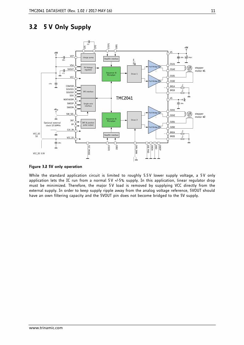
Figure 3.2 5V only operation
While the standard application circuit is limited to roughly 5.5 V lower supply voltage, a 5 V only application lets the IC run from a normal 5 V +/-5% supply. In this application, linear regulator drop must be minimized. Therefore, the major 5 V load is removed by supplying VCC directly from the external supply. In order to keep supply ripple away from the analog voltage reference, 5VOUT should have an own filtering capacity and the 5VOUT pin does not become bridged to the 5V supply.
TMC2041 DATASHEET (Rev. 1.02 / 2017-MAY-16) 12
www.trinamic.com
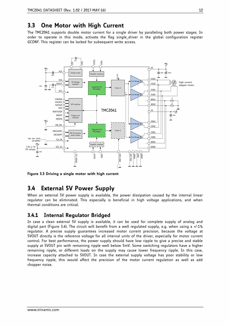
3.3 One Motor with High Current The TMC2041 supports double motor current for a single driver by paralleling both power stages. In order to operate in this mode, activate the flag single_driver in the global configuration register GCONF. This register can be locked for subsequent write access.
VCC_IO
SPI interface
CSN/IO0
SCK/IO1
SDO
SDI/IO2
Single wire interface
5V Voltage regulator
charge pumpVCP
22n
100n
SWION
SW_SEL
CLK_IN
SWIOP
+VM
5VOUT
VSA
4.7µ
+VIO
ENC1A/INT
ENC1B/PPINT & position pulse output
NEXTADDRDRV_EN
N
DRV_E
NN
GNDP
GND
GNDA
TST_M
ODE
DIE P
AD
VCC
opt. ext. clock12-16MHz
3.3V or 5VI/O voltage
100n
100n
Full Bridge A
Full Bridge B
+VM
VS
high current stepper motor
NS
O1A1
O1A2
BR1A
RS1B
O1B1
O1B2
Driver 1
100n
BR1B
RS1A
Full Bridge A
Full Bridge B
O2A1
O2A2
BR2A
O2B1
O2B2
Driver 2
BR2B
VS
100n
+VM
100µFCPI
CPO
+VIO
Step/Dir interface
STE
P1
DIR
1
Step/Dir interface
Sequencer & Microplyer
Sequencer & Microplyer
STEP
2
DIR
2
TMC2041
Figure 3.3 Driving a single motor with high current
3.4 External 5V Power Supply When an external 5V power supply is available, the power dissipation caused by the internal linear regulator can be eliminated. This especially is beneficial in high voltage applications, and when thermal conditions are critical.
3.4.1 Internal Regulator Bridged In case a clean external 5V supply is available, it can be used for complete supply of analog and digital part (Figure 3.4). The circuit will benefit from a well regulated supply, e.g. when using a +/-1% regulator. A precise supply guarantees increased motor current precision, because the voltage at 5VOUT directly is the reference voltage for all internal units of the driver, especially for motor current control. For best performance, the power supply should have low ripple to give a precise and stable supply at 5VOUT pin with remaining ripple well below 5mV. Some switching regulators have a higher remaining ripple, or different loads on the supply may cause lower frequency ripple. In this case, increase capacity attached to 5VOUT. In case the external supply voltage has poor stability or low frequency ripple, this would affect the precision of the motor current regulation as well as add chopper noise.

TMC2041 DATASHEET (Rev. 1.02 / 2017-MAY-16) 13
www.trinamic.com
5V Voltage regulator
+5V
5VOUT
VSA
4.7µ
VCC
470n
10R
Well-regulated, stable supply, better than +-5%
Figure 3.4 Using an external 5V supply to bypass internal regulator
3.5 Optimizing Analog Precision The 5VOUT pin is used as an analog reference for operation of the TMC2041. Performance will degrade when there is voltage ripple on this pin. Most of the high frequency ripple in a TMC2041 design results from the operation of the internal digital logic. The digital logic switches with each edge of the clock signal. Further, ripple results from operation of the charge pump, which operates with roughly 1 MHz and draws current from the VCC pin. In order to keep this ripple as low as possible, an additional filtering capacitor can be put directly next to the VCC pin with vias to the GND plane giving a short connection to the digital GND pins (pin 6 and pin 34). Analog performance is best, when this ripple is kept away from the analog supply pin 5VOUT, using an additional series resistor of 2.2 Ω. The voltage drop on this resistor will be roughly 100 mV (IVCC * R).
5V Voltage regulator
charge pumpVCP
22n
100n
+VM
5VOUT
VSA
4.7µ
VCC
100n
470n
CPI
CPO
GNDA
2R2
Figure 3.5 RC-Filter on VCC for reduced ripple
3.6 Driver Protection and EME Circuitry Some applications have to cope with ESD events caused by motor operation or external influence. Despite ESD circuitry within the driver chips, ESD events occurring during operation can cause a reset or even a destruction of the motor driver, depending on their energy. Especially plastic housings and belt drive systems tend to cause ESD events. It is best practice to avoid ESD events by attaching all conductive parts, especially the motors themselves to PCB ground, or to apply electrically conductive plastic parts. In addition, the driver can be protected up to a certain degree against ESD events or live plugging / pulling the motor, which also causes high voltages and high currents into the motor connector terminals. A simple scheme uses capacitors at the driver outputs to reduce the dV/dt caused by ESD events. Larger capacitors will bring more benefit concerning ESD suppression, but cause additional current flow in each chopper cycle, and thus increase driver power dissipation, especially at high supply voltages. The values shown are example values – they might be varied between 100pF and 1nF. The capacitors also dampen high frequency noise injected from digital parts of the circuit and thus reduce electromagnetic emission. A more elaborate scheme uses LC filters to de-couple the driver outputs from the motor connector. Varistors in between of the coil terminals eliminate coil overvoltage caused by live plugging. Optionally protect all outputs by a varistor against ESD voltage.

TMC2041 DATASHEET (Rev. 1.02 / 2017-MAY-16) 14
www.trinamic.com
Full Bridge A
Full Bridge B
steppermotor
NS
OA1
OA2
OB1
OB2
Driver
470pF
100V
470pF
100V
470pF
100V
470pF
100V
Full Bridge A
Full Bridge B
steppermotor
NS
OA1
OA2
OB1
OB2
Driver
470pF
100V
470pF
100V
50Ohm @
100MHz
50Ohm @
100MHz
50Ohm @
100MHz
50Ohm @
100MHz
V1
V2
Fit varistors to supply voltage
rating. SMD inductivities
conduct full motor coil
current.
470pF
100V
470pF
100V
Varistors V1 and V2 protect
against inductive motor coil
overvoltage.
V1A, V1B, V2A, V2B:
Optional position for varistors
in case of heavy ESD events.
BRB
RSA
BRA
100nF
16V
RSB100nF
16V
V1A
V1B
V2A
V2B
Figure 3.6 Simple ESD enhancement and more elaborate motor output protection

TMC2041 DATASHEET (Rev. 1.02 / 2017-MAY-16) 15
www.trinamic.com
4 SPI Interface
4.1 SPI Datagram Structure The TMC2041 uses 40 bit SPI™ (Serial Peripheral Interface, SPI is Trademark of Motorola) datagrams for communication with a microcontroller. Microcontrollers which are equipped with hardware SPI are typically able to communicate using integer multiples of 8 bit. The NCS line of the TMC2041 must be handled in a way, that it stays active (low) for the complete duration of the datagram transmission. Each datagram sent to the device is composed of an address byte followed by four data bytes. This allows direct 32 bit data word communication with the register set. Each register is accessed via 32 data bits even if it uses less than 32 data bits. For simplification, each register is specified by a one byte address:
- For a read access the most significant bit of the address byte is 0. - For a write access the most significant bit of the address byte is 1.
Most registers are write only registers, some can be read additionally, and there are also some read only registers.
4.1.1 Selection of Write / Read (WRITE_notREAD) The read and write selection is controlled by the MSB of the address byte (bit 39 of the SPI datagram). This bit is 0 for read access and 1 for write access. So, the bit named W is a WRITE_notREAD control bit. The active high write bit is the MSB of the address byte. So, 0x80 has to be added to the address for a write access. The SPI interface always delivers data back to the master, independent of the W bit. The data transferred back is the data read from the address which was transmitted with the previous datagram, if the previous access was a read access. If the previous access was a write access, then the data read back mirrors the previously received write data. So, the difference between a read and a write access is that the read access does not transfer data to the addressed register but it transfers the address only and its 32 data bits are dummies, and, further the following read or write access delivers back the data read from the address transmitted in the preceding read cycle.
A read access request datagram uses dummy write data. Read data is transferred back to the master with the subsequent read or write access. Hence, reading multiple registers can be done in a pipelined fashion.
Whenever data is read from or written to the TMC2041, the MSBs delivered back contain the SPI status, SPI_STATUS, a number of eight selected status bits.
SPI DATAGRAM STRUCTURE
MSB (transmitted first) 40 bit LSB (transmitted last)
39 ... ... 0
8 bit address 8 bit SPI status
32 bit data
39 ... 32 31 ... 0 to TMC2041: RW + 7 bit address from TMC2041: 8 bit SPI status
8 bit data 8 bit data 8 bit data 8 bit data
39 / 38 ... 32 31 ... 24 23 ... 16 15 ... 8 7 ... 0 W 38...32 31...28 27...24 23...20 19...16 15...12 11...8 7...4 3...0
39
38
37
36
35
34
33
32
31
30
29
28
27
26
25
24
23
22
21
20
19
18
17
16
15
14
13
12
11
10
9 8 7 6 5 4 3 2 1 0

TMC2041 DATASHEET (Rev. 1.02 / 2017-MAY-16) 16
www.trinamic.com
Example: For a read access to the register (XACTUAL) with the address 0x21, the address byte has to be set to 0x21 in the access preceding the read access. For a write access to the register (VACTUAL), the address byte has to be set to 0x80 + 0x22 = 0xA2. For read access, the data bit might have any value (-). So, one can set them to 0. action data sent to TMC2041 data received from TMC2041
read CHOPCONF1 0x6C00000000 0xSS & unused data
read CHOPCONF1 0x6C00000000 0xSS & CHOPCONF1
write CHOPCONF1:= 0x00ABCDEF 0xEC00ABCDEF 0xSS & CHOPCONF1
write CHOPCONF1:= 0x00123456 0xEC00123456 0xSS00ABCDEF
*)S: is a placeholder for the status bits SPI_STATUS
4.1.2 SPI Status Bits Transferred with Each Datagram Read Back New status information becomes latched at the end of each access and is available with the next SPI transfer.
SPI_STATUS – status flags transmitted with each SPI access in bits 39 to 32
Bit Name Comment
7 - reserved (0)
6 - reserved (0)
5 - reserved (0)
4 - reserved (0)
3 - reserved (0)
2 driver_error(2) GSTAT[2] – 1: Signals driver 2 driver error (clear by reading GSTAT)
1 driver_error(1) GSTAT[1] – 1: Signals driver 1 driver error (clear by reading GSTAT)
0 reset_flag GSTAT[0] – 1: Signals, that a reset has occurred (clear by reading GSTAT)
4.1.3 Data Alignment All data are right aligned. Some registers represent unsigned (positive) values, some represent integer values (signed) as two’s complement numbers, single bits or groups of bits are represented as single bits respectively as integer groups.
4.2 SPI Signals The SPI bus on the TMC2041 has four signals:
- SCK – bus clock input - SDI – serial data input - SDO – serial data output - CSN – chip select input (active low)
The slave is enabled for an SPI transaction by a low on the chip select input CSN. Bit transfer is synchronous to the bus clock SCK, with the slave latching the data from SDI on the rising edge of SCK and driving data to SDO following the falling edge. The most significant bit is sent first. A minimum of 40 SCK clock cycles is required for a bus transaction with the TMC2041.
If more than 40 clocks are driven, the additional bits shifted into SDI are shifted out on SDO after a 40-clock delay through an internal shift register. This can be used for daisy chaining multiple chips.
CSN must be low during the whole bus transaction. When CSN goes high, the contents of the internal shift register are latched into the internal control register and recognized as a command from the master to the slave. If more than 40 bits are sent, only the last 40 bits received before the rising edge of CSN are recognized as the command.

TMC2041 DATASHEET (Rev. 1.02 / 2017-MAY-16) 17
www.trinamic.com
4.3 Timing The SPI interface is synchronized to the internal system clock, which limits the SPI bus clock SCK to half of the system clock frequency. If the system clock is based on the on-chip oscillator, an additional 10% safety margin must be used to ensure reliable data transmission. All SPI inputs as well as the ENN input are internally filtered to avoid triggering on pulses shorter than 20ns. Figure 4.1 shows the timing parameters of an SPI bus transaction, and the table below specifies their values.
CSN
SCK
SDI
SDO
tCC tCCtCL tCH
bit39 bit38 bit0
bit39 bit38 bit0
tDO tZC
tDU tDH
tCH
Figure 4.1 SPI timing
Hint Usually this SPI timing is referred to as SPI MODE 3
SPI interface timing AC-Characteristics
clock period: tCLK
Parameter Symbol Conditions Min Typ Max Unit
SCK valid before or after change of CSN
tCC
10 ns
CSN high time tCSH
*) Min time is for synchronous CLK with SCK high one tCH before CSN high only
tCLK*) >2tCLK+10 ns
SCK low time tCL *) Min time is for synchronous CLK only
tCLK*) >tCLK+10 ns
SCK high time tCH *) Min time is for synchronous CLK only
tCLK*) >tCLK+10 ns
SCK frequency using internal clock
fSCK assumes minimum OSC frequency 4 MHz
SCK frequency using external 16MHz clock
fSCK assumes synchronous CLK 8 MHz
SDI setup time before rising edge of SCK
tDU
10 ns
SDI hold time after rising edge of SCK
tDH
10 ns
Data out valid time after falling SCK clock edge
tDO no capacitive load on SDO tFILT+5 ns
SDI, SCK and CSN filter delay time
tFILT rising and falling edge 12 20 30 ns

TMC2041 DATASHEET (Rev. 1.02 / 2017-MAY-16) 18
www.trinamic.com
5 UART Single Wire Interface The UART single wire interface allows the control of the TMC2041 with any microcontroller UART. It shares transmit and receive line like an RS485 based interface. Data transmission is secured using a cyclic redundancy check, so that increased interface distances (e.g. over cables between two PCBs) can be bridged without the danger of wrong or missed commands even in the event of electro-magnetic disturbance. The automatic baud rate detection and an advanced addressing scheme make this interface easy and flexible to use.
5.1 Datagram Structure 5.1.1 Write Access
UART WRITE ACCESS DATAGRAM STRUCTURE
each byte is LSB…MSB, highest byte transmitted first
0 … 63
sync + reserved 8 bit slave address
RW + 7 bit register addr.
32 bit data CRC
0…7 8…15 16…23 24…55 56…63
1 0 1 0 Reserved (don’t cares but included in CRC)
SLAVEADDR register address
1 data bytes 3, 2, 1, 0 (high to low byte)
CRC
0
1
2
3
4
5
6
7
8
…
15
16 …
23
24 …
55
56 …
63
A sync nibble precedes each transmission to and from the TMC2041 and is embedded into the first transmitted byte, followed by an addressing byte. Each transmission allows a synchronization of the internal baud rate divider to the master clock. The actual baud rate is adapted and variations of the internal clock frequency are compensated. Thus, the baud rate can be freely chosen within the valid range. Each transmitted byte starts with a start bit (logic 0, low level on SWIOP) and ends with a stop bit (logic 1, high level on SWIOP). The bit time is calculated by measuring the time from the beginning of start bit (1 to 0 transition) to the end of the sync frame (1 to 0 transition from bit 2 to bit 3). All data is transmitted byte wise. The 32 bit data words are transmitted with the highest byte first. A minimum baud rate of 9000 baud is permissible, assuming 20 MHz clock (worst case for low baud rate). Maximum baud rate is fCLK/16 due to the required stability of the baud clock. The slave address is determined by the register SLAVEADDR. If the external address pin NEXTADDR is set, the slave address becomes incremented by one. The communication becomes reset if a pause time of longer than 63 bit times between the start bits of two successive bytes occurs. This timing is based on the last correctly received datagram. In this case, the transmission needs to be restarted after a failure recovery time of minimum 12 bit times of bus idle time. This scheme allows the master to reset communication in case of transmission errors. Any pulse on an idle data line below 16 clock cycles will be treated as a glitch and leads to a timeout of 12 bit times, for which the data line must be idle. Other errors like wrong CRC are also treated the same way. This allows a safe re-synchronization of the transmission after any error conditions. Remark, that due to this mechanism, an abrupt reduction of the baud rate to less than 15 percent of the previous value is not possible. Each accepted write datagram becomes acknowledged by the receiver by incrementing an internal cyclic datagram counter (8 bit). Reading out the datagram counter allows the master to check the success of an initialization sequence or single write accesses. Read accesses do not modify the counter.
TMC2041 DATASHEET (Rev. 1.02 / 2017-MAY-16) 19
www.trinamic.com
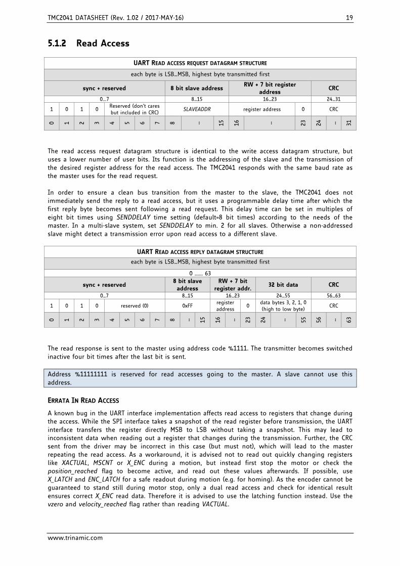
5.1.2 Read Access
UART READ ACCESS REQUEST DATAGRAM STRUCTURE
each byte is LSB…MSB, highest byte transmitted first
sync + reserved 8 bit slave address RW + 7 bit register
address CRC
0...7 8…15 16…23 24…31
1 0 1 0 Reserved (don’t cares but included in CRC)
SLAVEADDR register address 0 CRC
0
1
2
3
4
5
6
7
8
…
15
16 …
23
24 …
31
The read access request datagram structure is identical to the write access datagram structure, but uses a lower number of user bits. Its function is the addressing of the slave and the transmission of the desired register address for the read access. The TMC2041 responds with the same baud rate as the master uses for the read request. In order to ensure a clean bus transition from the master to the slave, the TMC2041 does not immediately send the reply to a read access, but it uses a programmable delay time after which the first reply byte becomes sent following a read request. This delay time can be set in multiples of eight bit times using SENDDELAY time setting (default=8 bit times) according to the needs of the master. In a multi-slave system, set SENDDELAY to min. 2 for all slaves. Otherwise a non-addressed slave might detect a transmission error upon read access to a different slave.
UART READ ACCESS REPLY DATAGRAM STRUCTURE
each byte is LSB…MSB, highest byte transmitted first
0 ...... 63
sync + reserved 8 bit slave address
RW + 7 bit register addr.
32 bit data CRC
0…7 8…15 16…23 24…55 56…63
1 0 1 0 reserved (0) 0xFF register address
0 data bytes 3, 2, 1, 0 (high to low byte)
CRC
0
1
2
3
4
5
6
7
8
…
15
16 …
23
24 …
55
56 …
63
The read response is sent to the master using address code %1111. The transmitter becomes switched inactive four bit times after the last bit is sent.
Address %11111111 is reserved for read accesses going to the master. A slave cannot use this address.
ERRATA IN READ ACCESS
A known bug in the UART interface implementation affects read access to registers that change during the access. While the SPI interface takes a snapshot of the read register before transmission, the UART interface transfers the register directly MSB to LSB without taking a snapshot. This may lead to inconsistent data when reading out a register that changes during the transmission. Further, the CRC sent from the driver may be incorrect in this case (but must not), which will lead to the master repeating the read access. As a workaround, it is advised not to read out quickly changing registers like XACTUAL, MSCNT or X_ENC during a motion, but instead first stop the motor or check the position_reached flag to become active, and read out these values afterwards. If possible, use X_LATCH and ENC_LATCH for a safe readout during motion (e.g. for homing). As the encoder cannot be guaranteed to stand still during motor stop, only a dual read access and check for identical result ensures correct X_ENC read data. Therefore it is advised to use the latching function instead. Use the vzero and velocity_reached flag rather than reading VACTUAL.

TMC2041 DATASHEET (Rev. 1.02 / 2017-MAY-16) 20
www.trinamic.com
5.2 CRC Calculation An 8 bit CRC polynomial is used for checking both read and write access. It allows detection of up to eight single bit errors. The CRC8-ATM polynomial with an initial value of zero is applied LSB to MSB, including the sync- and addressing byte. The sync nibble is assumed to always be correct. The TMC2041 responds only to correctly transmitted datagrams containing its own slave address. It increases its datagram counter for each correctly received write access datagram.
𝐶𝑅𝐶 = 𝑥8 + 𝑥2 + 𝑥1 + 𝑥0 SERIAL CALCULATION EXAMPLE
CRC = (CRC << 1) OR (CRC.7 XOR CRC.1 XOR CRC.0 XOR [new incoming bit])
C-CODE EXAMPLE FOR CRC CALCULATION
void swuart_calcCRC(UCHAR* datagram, UCHAR datagramLength)
int i,j;
UCHAR* crc = datagram + (datagramLength-1); // CRC located in last byte of message
UCHAR currentByte;
*crc = 0;
for (i=0; i<(datagramLength-1); i++) // Execute for all bytes of a message
currentByte = datagram[i]; // Retrieve a byte to be sent from Array
for (j=0; j<8; j++)
if ((*crc >> 7) ^ (currentByte&0x01)) // update CRC based result of XOR operation
*crc = (*crc << 1) ^ 0x07;
else
*crc = (*crc << 1);
currentByte = currentByte >> 1;
// for CRC bit
// for message byte
5.3 UART Signals The UART interface on the TMC2041 has following signals:
TMC2041 UART INTERFACE SIGNALS
SWIOP Non-inverted data input and output
SWION Inverted data input and output for use in differential transmission. Can be left open in a 5V IO voltage system. Tie to the half IO level voltage for best performance in a 3.3V single wire non-differential application.
NEXTADDR Address increment pin for sequential addressing scheme
SDO Configuration input: Tie low for standard mode!
In UART mode (SW_SEL high) the slave checks the single wire SWIOP and SWION for correctly received datagrams with its own address continuously. Both signals are switched as input during this time. It adapts to the baud rate based on the sync nibble, as described before. In case of a read access, it switches on its output drivers on SWIOP and SWION and sends its response using the same baud rate.

TMC2041 DATASHEET (Rev. 1.02 / 2017-MAY-16) 21
www.trinamic.com
5.4 Addressing Multiple Slaves
ADDRESSING ONE OR TWO SLAVES
If only one or two TMC2041 are addressed by a master using a single UART interface, a hardware address selection can be done by setting the NEXTADDR pins to different levels.
ADDRESSING UP TO 255 SLAVES
A different approach can address any number of devices by using the input NEXTADDR as a selection pin. Addressing up to 255 units is possible.
Master CPU (µC with UART,
software switches TXD to
hi-Z for receiving)
TMC2041#1NEXTADDR
CSN/IO0
SW
IOP
SW
ION
TMC2041#2NEXTADDR
SW
IOP
SW
ION
+VIO
CSN/IO0
TMC2041#3NEXTADDR
SW
IOP
SW
ION
+VIO
TXDRIDLE
+VIO
RIDLE forces stop bit level in idle conditions, 3k3 is sufficient with 14 slaves
RXD
10k 10k
address 0, IO0 is high-Z address 1 address 1
program to address 254 & set IO0 low address 0, IO0 is high-Z address 1
address 254 program to address 253 & set IO0 low address 0
address 254 address 253 program to address 252 & set IO0 low
Addressing phase 1:
Addressing phase 2:
Addressing phase 3:
Addressing phase 4:
EXAMPLE FOR ADDRESSING UP TO 255 TMC2041
Addressing phase X: continue procedure
Figure 5.1 Addressing multiple TMC2041 via single wire interface using chaining
Proceed as follows:
- Tie the NEXTADDR pin of your first TMC2041 to GND. - Interconnect one of the general purpose IO-pins of the first TMC2041 to the next drivers
NEXTADDR pin using an additional pull-up resistor. Connect further drivers in the same fashion.
- Now, the first driver responds to address 0. Following drivers are set to address 1. - Program the first driver to its dedicated slave address. Note: once a driver is initialized with
its slave address, its general purpose output, which is tied to the next drivers NEXTADDR has to be programmed as output and set to 0.
- Now, the second driver is accessible and can get its slave address. Further units can be programmed to their slave addresses sequentially.

TMC2041 DATASHEET (Rev. 1.02 / 2017-MAY-16) 22
www.trinamic.com
Master CPU (µC with RS485
tranceiver)
TMC2041#1NEXTADDR
CSN/IO0
SW
IOP
SW
ION
TMC2041#2NEXTADDR
SW
IOP
SW
ION
TMC2041#3
SW
IOP
SW
ION
A
B
Addressing phase 1: address 0, IO0 high address 1 address 1
Addressing phase 2: program to address 254 & set IO0 low address 0, IO0 high address 1
Addressing phase 3: address 254 program to address 253 & set NAO low address 0, IO0 high
Addressing phase 4: address 254 address 253 program to address 252 & set IO0 low
1k
+VIO
CSN/IO0
NEXTADDR
EXAMPLE FOR ADDRESSING UP TO 255 TMC2041
Addressing phase X: continue procedure
RTERM RTERM
RFILT
CFILT
RFILT
CFILT
+VIO
10k
+VIO
10k
Figure 5.2 Addressing multiple TMC2041 via differential interface, additional filtering for NEXTADDR
A different scheme (not shown) uses bus switches (like 74HC4066) to connect the bus to the next unit in the chain without using the NAI input. The bus switch can be controlled in the same fashion, using the NAO output to enable it (low level shall enable the bus switch). Once the bus switch is enabled it allows addressing the next bus segment. As bus switches add a certain resistance, the maximum number of nodes will be reduced.
It is possible to mix different styles of addressing in a system. For example a system using two boards with each two TMC2041 can have both devices on a board with a different level on NEXTADDR, while the next board is chained using analog switches separating the bus until the drivers on the first board have been programmed.

TMC2041 DATASHEET (Rev. 1.02 / 2017-MAY-16) 23
www.trinamic.com
6 Register Mapping This chapter gives an overview of the complete register set. Some of the registers bundling a number of single bits are detailed in extra tables. The functional practical application of the settings is detailed in dedicated chapters.
Note - All registers become reset to 0 upon power up, unless otherwise noted. - Add 0x80 to the address Addr for write accesses!
NOTATION OF HEXADECIMAL AND BINARY NUMBERS
0x precedes a hexadecimal number, e.g. 0x04
% precedes a multi-bit binary number, e.g. %100
NOTATION OF R/W FIELD
R Read only
W Write only
R/W Read- and writable register
R+C Clear upon read
OVERVIEW REGISTER MAPPING
REGISTER DESCRIPTION
General Configuration Registers These registers contain
- global configuration
- global status flags
- slave address configuration
- and I/O configuration
Current Setting This register set offers registers for
- driver current control and hold current
Motor Driver Register Set This register set offers registers for
- chopper and driver configuration
- coolStep and stallGuard2 configuration
TMC2041 DATASHEET (Rev. 1.02 / 2017-MAY-16) 24
www.trinamic.com
6.1 General Configuration Registers
GENERAL CONFIGURATION REGISTERS (0X00…0X0F)
R/W Addr n Register Description / bit names
RW 0x00 10 GCONF
Bit GCONF – Global configuration flags
0 single_driver 0: Two motors can be operated. 1: Single motor, double current operation - driver 2
outputs are identical to driver 1, all driver 2 related controls are unused in this mode.
Attention: Set correctly before driver enable!
1 stepdir1_enable 0: Driver 1 does not accept steps. 1: Step/Dir interface enabled via STEP1 and DIR1
2 stepdir2_enable 0: Driver 2 does not accept steps. 1: Step/Dir interface enabled via STEP2 and DIR2
3 reserved set to 0
4 reserved set to 0
5 reserved set to 0
6 reserved set to 0
7 test_mode 0: Normal operation 1: Enable analog test output on pin REFR2
SLAVEADDR selects the function of REFR2: 0…4: T120, DAC1, VDDH1, DAC2, VDDH2
Attention: Not for user, set to 0 for normal operation!
8 shaft1 1: Inverse motor 1 direction
9 shaft2 1: Inverse motor 2 direction
10 lock_gconf 1: GCONF is locked against further write access.

TMC2041 DATASHEET (Rev. 1.02 / 2017-MAY-16) 25
www.trinamic.com
GENERAL CONFIGURATION REGISTERS (0X00…0X0F)
R/W Addr n Register Description / bit names
R+C 0x01 4 GSTAT
Bit GSTAT – Global status flags
0 reset 1: Indicates that the IC has been reset since the last
read access to GSTAT. All registers have been cleared to reset values.
1 drv_err1 1: Indicates, that driver 1 has been shut down due
to overtemperature or short circuit detection since the last read access. Read DRV_STATUS1 for details. The flag can only be reset when all error conditions are cleared.
2 drv_err2 1: Indicates, that driver 2 has been shut down due
to overtemperature or short circuit detection since the last read access. Read DRV_STATUS2 for details. The flag can only be reset when all error conditions are cleared.
3 uv_cp 1: Indicates an undervoltage on the charge pump.
The driver is disabled in this case.
R 0x02 8 IFCNT
Interface transmission counter. This register becomes incremented with each successful UART interface write access. It can be read out to check the serial transmission for lost data. Read accesses do not change the content. Disabled in SPI operation. The counter wraps around from 255 to 0.
W 0x03 8 + 4
SLAVECONF
Bit SLAVECONF
7..0 SLAVEADDR: Sets the address of unit for the UART interface. The address becomes incremented by one when the external address pin NEXTADDR is active. Range: 0-253 (254), default=0 In ring mode, 0 disables forwarding.
11..8 SENDDELAY: 0, 1: 8 bit times (not allowed with multiple slaves) 2, 3: 3*8 bit times 4, 5: 5*8 bit times 6, 7: 7*8 bit times 8, 9: 9*8 bit times 10, 11: 11*8 bit times 12, 13: 13*8 bit times 14, 15: 15*8 bit times
R 0x04 9 + 8
INPUT
Bit INPUT
Reads the digital state of all input pins available plus the state of IO pins set to output.
0 io0_in: IO0 polarity
1 io1_in: IO1 polarity
2 io2_in: IO2 polarity
3 io3_in: IO3 polarity
4 iop_in: IOP pin polarity (always input in SPI mode)
5 ion_in: ION pin polarity (always input in SPI mode)
6 nextaddr_in: NEXTADDR pin polarity
7 drv_enn_in: DRV_ENN pin polarity
8 sw_comp_in: UART input comparator (1: IOP voltage is above ION voltage). The accuracy is about 20mV.

TMC2041 DATASHEET (Rev. 1.02 / 2017-MAY-16) 26
www.trinamic.com
GENERAL CONFIGURATION REGISTERS (0X00…0X0F)
R/W Addr n Register Description / bit names
31.. 24
VERSION: 0x10=version of the IC Identical numbers mean full digital compatibility.
W 4 + 4
OUTPUT
Bit OUTPUT
Sets the IO output pin polarity and data direction.
0 io0_out: IO0 output polarity
1 io1_out: IO1 output polarity
2 io2_out: IO2 output polarity
3 -
8 ioddr0 (IO0: 0=input, 1=output)
9 ioddr1 (IO1: 0=input, 1=output)
10 ioddr2 (IO2: 0=input, 1=output)
11 - (IO3 is always input)
Addresses Addr are specified for motor 1 (upper value) and motor 2 (second address).
6.2 Current Setting
RAMP GENERATOR DRIVER FEATURE CONTROL REGISTER SET (MOTOR 1: 0X30…0X36, MOTOR 2: 0X50…0X56)
R/W Addr n Register Description / bit names
W 0x30 0x50
5 + 5 + 4
IHOLD_IRUN
Bit IHOLD_IRUN – Driver current control
4..0 IHOLD Standstill current (0=1/32…31=32/32)
12..8 IRUN Motor run current (0=1/32…31=32/32) Hint: Choose sense resistors in a way, that normal IRUN is 16 to 31 for best microstep performance.
19..16 IHOLDDELAY Controls the number of clock cycles for motor power down after a motion as soon as TZEROWAIT has expired. The smooth transition avoids a motor jerk upon power down. 0: instant power down 1..15: Delay per current reduction step in multiple
of 2^18 clocks
TMC2041 DATASHEET (Rev. 1.02 / 2017-MAY-16) 27
www.trinamic.com
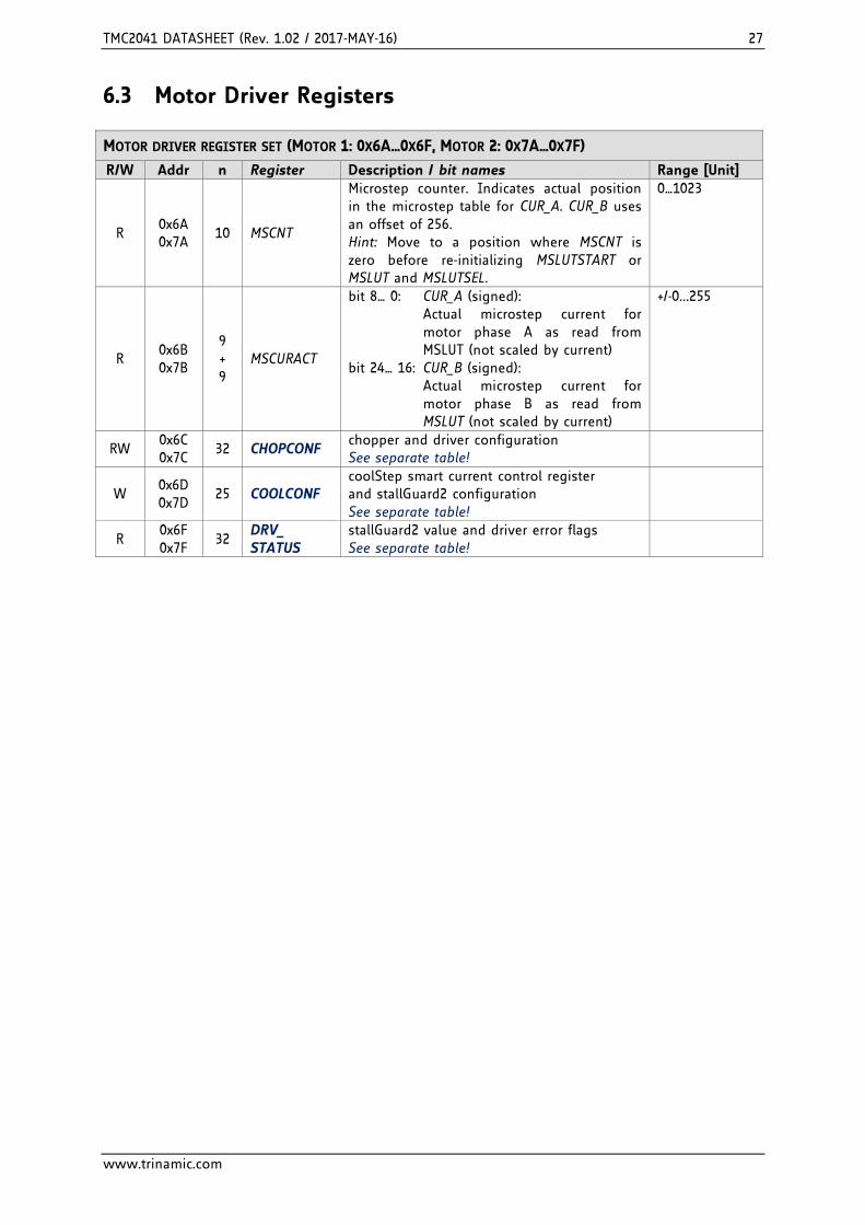
6.3 Motor Driver Registers
MOTOR DRIVER REGISTER SET (MOTOR 1: 0X6A…0X6F, MOTOR 2: 0X7A…0X7F)
R/W Addr n Register Description / bit names Range [Unit]
R 0x6A 0x7A
10 MSCNT
Microstep counter. Indicates actual position in the microstep table for CUR_A. CUR_B uses an offset of 256. Hint: Move to a position where MSCNT is zero before re-initializing MSLUTSTART or MSLUT and MSLUTSEL.
0…1023
R 0x6B 0x7B
9 + 9
MSCURACT
bit 8… 0: CUR_A (signed): Actual microstep current for
motor phase A as read from MSLUT (not scaled by current)
bit 24… 16: CUR_B (signed): Actual microstep current for
motor phase B as read from MSLUT (not scaled by current)
+/-0...255
RW 0x6C 0x7C
32 CHOPCONF chopper and driver configuration See separate table!
W 0x6D 0x7D
25 COOLCONF coolStep smart current control register and stallGuard2 configuration See separate table!
R 0x6F 0x7F
32 DRV_ STATUS
stallGuard2 value and driver error flags See separate table!

TMC2041 DATASHEET (Rev. 1.02 / 2017-MAY-16) 28
www.trinamic.com
6.3.1 CHOPCONF – Chopper Configuration 0X6C, 0X7C: CHOPCONF – CHOPPER CONFIGURATION
Bit Name Function Comment
31 - reserved set to 0
30 diss2g short to GND protection disable
0: Short to GND protection is on 1: Short to GND protection is disabled
29 dedge enable double edge step pulses
1: Enable step impulse at each step edge to reduce step frequency requirement.
28 intpol16 16 microsteps with interpolation
1: In 16 microstep mode, the microstep resolution becomes extrapolated to 256 microsteps for smoothest motor operation
27 mres3 MRES micro step resolution
%0000: Native 256 microstep setting. 26 mres2
25 mres1
24 mres0 %0001 … %1000: 128, 64, 32, 16, 8, 4, 2, FULLSTEP Reduced microstep resolution. The resolution gives the number of microstep entries per sine quarter wave. Especially when switching to a low resolution of 8 microsteps and below, take care to switch at certain microstep positions. The switching position determines the sequence of patterns.
step width=2^MRES [microsteps]
23 - reserved set to 0
22 -
21 -
20 -
19 - reserved set to 0
18 - reserved set to 0
17 vsense sense resistor voltage based current scaling
0: Low sensitivity, high sense resistor voltage 1: High sensitivity, low sense resistor voltage
16 tbl1 TBL blank time select
%00 … %11: Set comparator blank time to 16, 24, 36 or 54 clocks Hint: %01 or %10 recommended for most applications
15 tbl0
14 chm chopper mode 0 Standard mode (spreadCycle)
1
Constant off time with fast decay time. Fast decay time is also terminated when the negative nominal current is reached. Fast decay is after on time.
13 rndtf random TOFF time 0 Chopper off time is fixed as set by TOFF
1 Random mode, TOFF is random modulated by dNCLK= -12 … +3 clocks.
12 disfdcc fast decay mode chm=1: disfdcc=1 disables current comparator usage for termi-nation of the fast decay cycle
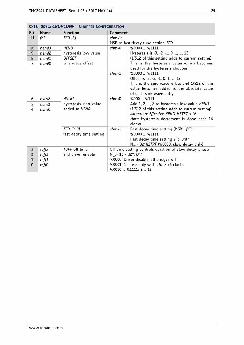
TMC2041 DATASHEET (Rev. 1.02 / 2017-MAY-16) 29
www.trinamic.com
0X6C, 0X7C: CHOPCONF – CHOPPER CONFIGURATION
Bit Name Function Comment
11 fd3 TFD [3] chm=1: MSB of fast decay time setting TFD
10 hend3 HEND hysteresis low value OFFSET sine wave offset
chm=0
%0000 … %1111: Hysteresis is -3, -2, -1, 0, 1, …, 12 (1/512 of this setting adds to current setting) This is the hysteresis value which becomes used for the hysteresis chopper.
9 hend2
8 hend1
7 hend0
chm=1 %0000 … %1111: Offset is -3, -2, -1, 0, 1, …, 12 This is the sine wave offset and 1/512 of the value becomes added to the absolute value of each sine wave entry.
6 hstrt2 HSTRT hysteresis start value added to HEND
chm=0
%000 … %111: Add 1, 2, …, 8 to hysteresis low value HEND (1/512 of this setting adds to current setting) Attention: Effective HEND+HSTRT ≤ 16. Hint: Hysteresis decrement is done each 16 clocks
5 hstrt1
4 hstrt0
TFD [2..0] fast decay time setting
chm=1 Fast decay time setting (MSB: fd3): %0000 … %1111: Fast decay time setting TFD with NCLK= 32*HSTRT (%0000: slow decay only)
3 toff3 TOFF off time and driver enable
Off time setting controls duration of slow decay phase NCLK= 12 + 32*TOFF %0000: Driver disable, all bridges off %0001: 1 – use only with TBL ≥ 36 clocks %0010 … %1111: 2 … 15
2 toff2
1 toff1
0 toff0
TMC2041 DATASHEET (Rev. 1.02 / 2017-MAY-16) 30
www.trinamic.com
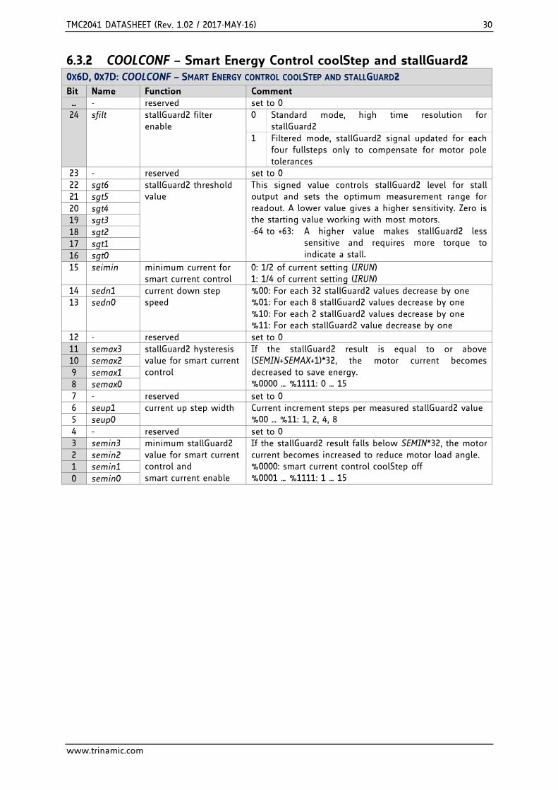
6.3.2 COOLCONF – Smart Energy Control coolStep and stallGuard2 0X6D, 0X7D: COOLCONF – SMART ENERGY CONTROL COOLSTEP AND STALLGUARD2
Bit Name Function Comment
… - reserved set to 0
24 sfilt
stallGuard2 filter enable
0 Standard mode, high time resolution for stallGuard2
1 Filtered mode, stallGuard2 signal updated for each four fullsteps only to compensate for motor pole tolerances
23 - reserved set to 0
22 sgt6 stallGuard2 threshold value
This signed value controls stallGuard2 level for stall output and sets the optimum measurement range for readout. A lower value gives a higher sensitivity. Zero is the starting value working with most motors. -64 to +63: A higher value makes stallGuard2 less
sensitive and requires more torque to indicate a stall.
21 sgt5
20 sgt4
19 sgt3
18 sgt2
17 sgt1
16 sgt0
15 seimin minimum current for smart current control
0: 1/2 of current setting (IRUN) 1: 1/4 of current setting (IRUN)
14 sedn1 current down step speed
%00: For each 32 stallGuard2 values decrease by one %01: For each 8 stallGuard2 values decrease by one %10: For each 2 stallGuard2 values decrease by one %11: For each stallGuard2 value decrease by one
13 sedn0
12 - reserved set to 0
11 semax3 stallGuard2 hysteresis value for smart current control
If the stallGuard2 result is equal to or above (SEMIN+SEMAX+1)*32, the motor current becomes decreased to save energy. %0000 … %1111: 0 … 15
10 semax2
9 semax1
8 semax0
7 - reserved set to 0
6 seup1 current up step width Current increment steps per measured stallGuard2 value %00 … %11: 1, 2, 4, 8 5 seup0
4 - reserved set to 0
3 semin3 minimum stallGuard2 value for smart current control and smart current enable
If the stallGuard2 result falls below SEMIN*32, the motor current becomes increased to reduce motor load angle. %0000: smart current control coolStep off %0001 … %1111: 1 … 15
2 semin2
1 semin1
0 semin0

TMC2041 DATASHEET (Rev. 1.02 / 2017-MAY-16) 31
www.trinamic.com
6.3.3 DRV_STATUS – stallGuard2 Value and Driver Error Flags 0X6F, 0X7F: DRV_STATUS – STALLGUARD2 VALUE AND DRIVER ERROR FLAGS
Bit Name Function Comment
31 stst standstill indicator This flag indicates motor stand still in each operation mode. It is especially useful for step & dir mode.
30 olb open load indicator phase B
1: Open load detected on phase A or B. Hint: This is just an informative flag. The driver takes no action upon it. False detection may occur in fast motion and standstill. Check during slow motion or after a motion, only.
29 ola open load indicator phase A
28 s2gb short to ground indicator phase B
1: Short to GND detected on phase A or B. The driver becomes disabled. The flags stay active, until the driver is disabled by software (TOFF=0) or by the ENN input. 27 s2ga short to ground
indicator phase A
26 otpw overtemperature pre-warning flag
1: Overtemperature pre-warning threshold is exceeded. The overtemperature pre-warning flag is common for both drivers.
25 ot overtemperature flag 1: Overtemperature limit has been reached. Drivers become disabled until otpw is also cleared due to cooling down of the IC. The overtemperature flag is common for both drivers.
24 stallGuard stallGuard2 status 1: Motor stall detected (SG_RESULT=0) or dcStep stall in dcStep mode.
23 - reserved Ignore these bits
22
21
20 CS ACTUAL
actual motor current / smart energy current
Actual current control scaling, for monitoring smart energy current scaling controlled via settings in register COOLCONF, or for monitoring the function of the automatic current scaling.
19
18
17
16
15 - reserved Ignore this bit
14 - reserved Ignore these bits
13
12
11
10
9 SG_ RESULT
stallGuard2 result respectively PWM on time for coil A in stand still for motor temperature detection
Mechanical load measurement: The stallGuard2 result gives a means to measure mechanical motor load. A higher value means lower mechanical load. A value of 0 signals highest load. With optimum SGT setting, this is an indicator for a motor stall. The stall detection compares SG_RESULT to 0 in order to detect a stall. SG_RESULT is used as a base for coolStep operation, by comparing it to a programmable upper and a lower limit.
stallGuard2 works best with microstep operation.
Temperature measurement: In standstill, no stallGuard2 result can be obtained. SG_RESULT shows the chopper on-time for motor coil A instead. If the motor is moved to a determined microstep position at a certain current setting, a comparison of the chopper on-time can help to get a rough estimation of motor temperature. As the motor heats up, its coil resistance rises and the chopper on-time increases.
8
7
6
5
4
3
2
1
0
TMC2041 DATASHEET (Rev. 1.02 / 2017-MAY-16) 32
www.trinamic.com
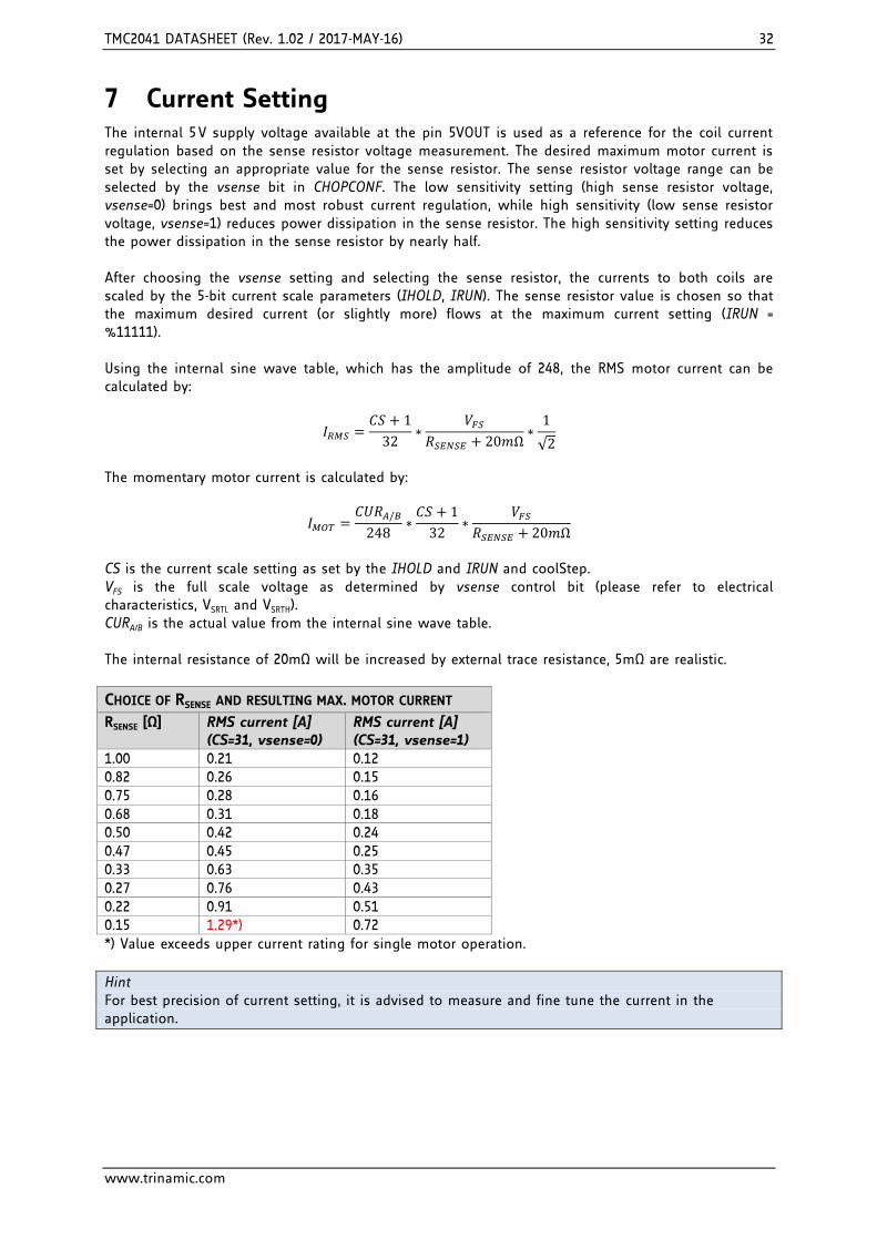
7 Current Setting The internal 5 V supply voltage available at the pin 5VOUT is used as a reference for the coil current regulation based on the sense resistor voltage measurement. The desired maximum motor current is set by selecting an appropriate value for the sense resistor. The sense resistor voltage range can be selected by the vsense bit in CHOPCONF. The low sensitivity setting (high sense resistor voltage, vsense=0) brings best and most robust current regulation, while high sensitivity (low sense resistor voltage, vsense=1) reduces power dissipation in the sense resistor. The high sensitivity setting reduces the power dissipation in the sense resistor by nearly half. After choosing the vsense setting and selecting the sense resistor, the currents to both coils are scaled by the 5-bit current scale parameters (IHOLD, IRUN). The sense resistor value is chosen so that the maximum desired current (or slightly more) flows at the maximum current setting (IRUN = %11111). Using the internal sine wave table, which has the amplitude of 248, the RMS motor current can be calculated by:
𝐼𝑅𝑀𝑆 =𝐶𝑆 + 1
32∗
𝑉𝐹𝑆
𝑅𝑆𝐸𝑁𝑆𝐸 + 20𝑚Ω∗
1
√2
The momentary motor current is calculated by:
𝐼𝑀𝑂𝑇 =𝐶𝑈𝑅𝐴/𝐵
248∗
𝐶𝑆 + 1
32∗
𝑉𝐹𝑆
𝑅𝑆𝐸𝑁𝑆𝐸 + 20𝑚Ω
CS is the current scale setting as set by the IHOLD and IRUN and coolStep. VFS is the full scale voltage as determined by vsense control bit (please refer to electrical characteristics, VSRTL and VSRTH). CURA/B is the actual value from the internal sine wave table. The internal resistance of 20mΩ will be increased by external trace resistance, 5mΩ are realistic.
CHOICE OF RSENSE AND RESULTING MAX. MOTOR CURRENT
RSENSE [Ω] RMS current [A] (CS=31, vsense=0)
RMS current [A] (CS=31, vsense=1)
1.00 0.21 0.12
0.82 0.26 0.15
0.75 0.28 0.16
0.68 0.31 0.18
0.50 0.42 0.24
0.47 0.45 0.25
0.33 0.63 0.35
0.27 0.76 0.43
0.22 0.91 0.51
0.15 1.29*) 0.72
*) Value exceeds upper current rating for single motor operation.
Hint For best precision of current setting, it is advised to measure and fine tune the current in the application.

TMC2041 DATASHEET (Rev. 1.02 / 2017-MAY-16) 33
www.trinamic.com
Parameter Description Setting Comment
IRUN Current scale when motor is running. Scales coil current values as taken from the internal sine wave table. For high precision motor operation, work with a current scaling factor in the range 16 to 31, because scaling down the current values reduces the effective microstep resolution by making microsteps coarser. This setting also controls the maximum current value set by coolStep.
0 … 31
scaling factor 1/32, 2/32, … 32/32
IHOLD Identical to IRUN, but for motor in stand still.
IHOLD DELAY
Allows smooth current reduction from run current to hold current. IHOLDDELAY controls the number of clock cycles for motor power down after TZEROWAIT in increments of 2^18 clocks: 0=instant power down, 1..15: Current reduction delay per current step in multiple of 2^18 clocks. Example: When using IRUN=31 and IHOLD=16, 15 current steps are required for hold current reduction. A IHOLDDELAY setting of 4 thus results in a power down time of 4*15*2^18 clock cycles, i.e. roughly one second at 16MHz.
0 instant IHOLD
1 …15
1*218 … 15*218 clocks per current decrement
vsense Allows control of the sense resistor voltage range for full scale current.
0 VFS = 0.32 V
1 VFS = 0.18 V
7.1 Sense Resistors Sense resistors should be carefully selected. The full motor current flows through the sense resistors. They also see the switching spikes from the MOSFET bridges. A low-inductance type such as film or composition resistors is required to prevent spikes causing ringing on the sense voltage inputs leading to unstable measurement results. A low-inductance, low-resistance PCB layout is essential. Any common GND path for the two sense resistors must be avoided, because this would lead to coupling between the two current sense signals. A massive ground plane is best. Please also refer to layout considerations in chapter 19. The sense resistor needs to be able to conduct the peak motor coil current in motor standstill conditions, unless standby power is reduced. Under normal conditions, the sense resistor conducts less than the coil RMS current, because no current flows through the sense resistor during the slow decay phases. The peak sense resistor power dissipation is:
𝑃𝑅𝑆𝑀𝐴𝑋 = 𝐼𝐶𝑂𝐼𝐿2 ∗ 𝑅𝑆𝐸𝑁𝑆𝐸
For high current applications, power dissipation is halved by using the low vsense setting and using an adapted resistance value. Please be aware, that in this case any voltage drop in PCB traces has a larger influence on the result. A compact layout with massive ground plane is best to avoid parasitic resistance effects.

TMC2041 DATASHEET (Rev. 1.02 / 2017-MAY-16) 34
www.trinamic.com
8 spreadCycle and Classic Chopper spreadCycle is a cycle-by-cycle current control. Therefore, it can react extremely fast to changes in motor velocity or motor load. The currents through both motor coils are controlled using choppers. The choppers work independently of each other. In Figure 8.1 the different chopper phases are shown.
RSENSE
ICOIL
On Phase: current flows in direction of target current
RSENSE
ICOIL
Fast Decay Phase: current flows in opposite direction of target current
RSENSE
ICOIL
Slow Decay Phase: current re-circulation
+VM +VM +VM
Figure 8.1 Chopper phases
Although the current could be regulated using only on phases and fast decay phases, insertion of the slow decay phase is important to reduce electrical losses and current ripple in the motor. The duration of the slow decay phase is specified in a control parameter and sets an upper limit on the chopper frequency. The current comparator can measure coil current during phases when the current flows through the sense resistor, but not during the slow decay phase, so the slow decay phase is terminated by a timer. The on phase is terminated by the comparator when the current through the coil reaches the target current. The fast decay phase may be terminated by either the comparator or another timer.
When the coil current is switched, spikes at the sense resistors occur due to charging and discharging parasitic capacitances. During this time, typically one or two microseconds, the current cannot be measured. Blanking is the time when the input to the comparator is masked to block these spikes.
There are two cycle-by-cycle chopper modes available: a new high-performance chopper algorithm called spreadCycle and a proven constant off-time chopper mode. The constant off-time mode cycles through three phases: on, fast decay, and slow decay. The spreadCycle mode cycles through four phases: on, slow decay, fast decay, and a second slow decay.
The chopper frequency is an important parameter for a chopped motor driver. A too low frequency might generate audible noise. A higher frequency reduces current ripple in the motor, but with a too high frequency magnetic losses may rise. Also power dissipation in the driver rises with increasing frequency due to the increased influence of switching slopes causing dynamic dissipation. Therefore, a compromise needs to be found. Most motors are optimally working in a frequency range of 16 kHz to 30 kHz. The chopper frequency is influenced by a number of parameter settings as well as by the motor inductivity and supply voltage.
Hint A chopper frequency in the range of 16 kHz to 30 kHz gives a good result for most motors when using spreadCycle. A higher frequency leads to increased switching losses. It is advised to check the resulting frequency and to work below 50 kHz.

TMC2041 DATASHEET (Rev. 1.02 / 2017-MAY-16) 35
www.trinamic.com
Three parameters are used for controlling both chopper modes:
8.1 spreadCycle Chopper The spreadCycle (patented) chopper algorithm is a precise and simple to use chopper mode which automatically determines the optimum length for the fast-decay phase. The spreadCycle will provide superior microstepping quality even with default settings. Several parameters are available to optimize the chopper to the application. Each chopper cycle is comprised of an on phase, a slow decay phase, a fast decay phase and a second slow decay phase (see Figure 8.3). The two slow decay phases and the two blank times per chopper cycle put an upper limit to the chopper frequency. The slow decay phases typically make up for about 30%-70% of the chopper cycle in standstill and are important for low motor and driver power dissipation. Calculation of a starting value for the slow decay time TOFF: Assumptions: Target Chopper frequency: 25kHz Two slow decay cycles make up for 50% of overall chopper cycle time
𝑡𝑂𝐹𝐹 =1
25𝑘𝐻𝑧∗
50
100∗
1
2= 10µ𝑠
For the TOFF setting this means: 𝑇𝑂𝐹𝐹 = (𝑡𝑂𝐹𝐹 ∗ 𝑓𝐶𝐿𝐾 − 12)/32
With 12 MHz clock this gives a setting of TOFF=3.4, i.e. 3 or 4. With 16 MHz clock this gives a setting of TOFF=4.6, i.e. 4 or 5. The hysteresis start setting forces the driver to introduce a minimum amount of current ripple into the motor coils. The current ripple must be higher than the current ripple which is caused by resistive losses in the motor in order to give best microstepping results. This will allow the chopper to precisely regulate the current both for rising and for falling target current. The time required to introduce the current ripple into the motor coil also reduces the chopper frequency. Therefore, a higher hysteresis setting will lead to a lower chopper frequency. The motor inductance limits the ability of the chopper to follow a changing motor current. Further the duration of the on phase and the fast decay must be longer than the blanking time, because the current comparator is disabled during blanking. It is easiest to find the best setting by starting from a low hysteresis setting (e.g. HSTRT=0, HEND=0) and increasing HSTRT, until the motor runs smoothly at low velocity settings. This can best be checked when measuring the motor current either with a current probe or by probing the sense resistor voltages (see Figure 8.2). Checking the sine wave shape near zero transition will show a small ledge between both half waves in case the hysteresis setting is too small. At medium velocities (i.e.
Parameter Description Setting Comment
TOFF Sets the slow decay time (off time). This setting also limits the maximum chopper frequency. Setting this parameter to zero completely disables all driver transistors and the motor can free-wheel.
0 chopper off
1…15 off time setting NCLK= 12 + 32*TOFF (1 will work with minimum blank time of 24 clocks)
TBL Selects the comparator blank time. This time needs to safely cover the switching event and the duration of the ringing on the sense resistor. For most applications, a setting of 1 or 2 is good. For highly capacitive loads, e.g. when filter networks are used, a setting of 2 or 3 will be required.
0 16 tCLK
1 24 tCLK
2 36 tCLK
3 54 tCLK
chm Selection of the chopper mode 0 spreadCycle
1 classic const. off time
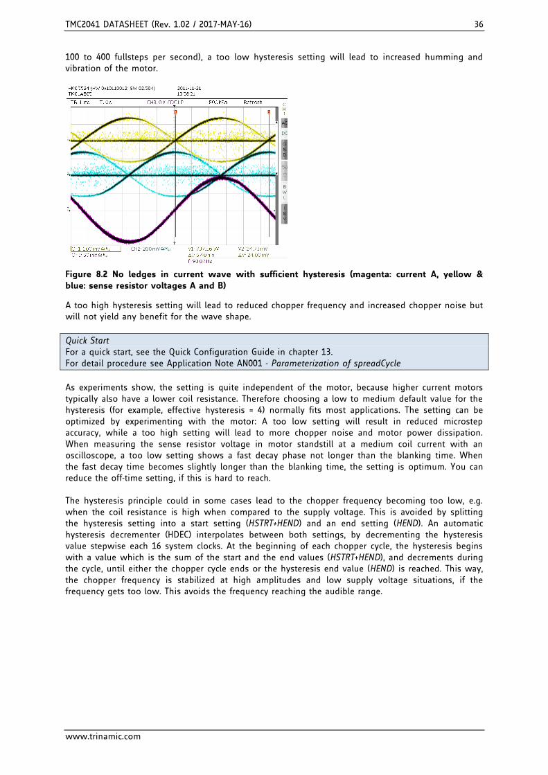
TMC2041 DATASHEET (Rev. 1.02 / 2017-MAY-16) 36
www.trinamic.com
100 to 400 fullsteps per second), a too low hysteresis setting will lead to increased humming and vibration of the motor.
Figure 8.2 No ledges in current wave with sufficient hysteresis (magenta: current A, yellow & blue: sense resistor voltages A and B)
A too high hysteresis setting will lead to reduced chopper frequency and increased chopper noise but will not yield any benefit for the wave shape.
Quick Start For a quick start, see the Quick Configuration Guide in chapter 13. For detail procedure see Application Note AN001 - Parameterization of spreadCycle
As experiments show, the setting is quite independent of the motor, because higher current motors typically also have a lower coil resistance. Therefore choosing a low to medium default value for the hysteresis (for example, effective hysteresis = 4) normally fits most applications. The setting can be optimized by experimenting with the motor: A too low setting will result in reduced microstep accuracy, while a too high setting will lead to more chopper noise and motor power dissipation. When measuring the sense resistor voltage in motor standstill at a medium coil current with an oscilloscope, a too low setting shows a fast decay phase not longer than the blanking time. When the fast decay time becomes slightly longer than the blanking time, the setting is optimum. You can reduce the off-time setting, if this is hard to reach. The hysteresis principle could in some cases lead to the chopper frequency becoming too low, e.g. when the coil resistance is high when compared to the supply voltage. This is avoided by splitting the hysteresis setting into a start setting (HSTRT+HEND) and an end setting (HEND). An automatic hysteresis decrementer (HDEC) interpolates between both settings, by decrementing the hysteresis value stepwise each 16 system clocks. At the beginning of each chopper cycle, the hysteresis begins with a value which is the sum of the start and the end values (HSTRT+HEND), and decrements during the cycle, until either the chopper cycle ends or the hysteresis end value (HEND) is reached. This way, the chopper frequency is stabilized at high amplitudes and low supply voltage situations, if the frequency gets too low. This avoids the frequency reaching the audible range.

TMC2041 DATASHEET (Rev. 1.02 / 2017-MAY-16) 37
www.trinamic.com
t
I
target current
target current - hysteresis start
target current + hysteresis start
on sd fd sd
target current + hysteresis end
target current - hysteresis end
HDEC
Figure 8.3 spreadCycle chopper scheme showing coil current during a chopper cycle
Two parameters control spreadCycle mode:
Parameter Description Setting Comment
HSTRT Hysteresis start setting. This value is an offset from the hysteresis end value HEND.
0…7 HSTRT=1…8
This value adds to HEND.
HEND Hysteresis end setting. Sets the hysteresis end value after a number of decrements. The sum HSTRT+HEND must be ≤16. At a current setting of max. 30 (amplitude reduced to 240), the sum is not limited.
0…2 -3…-1: negative HEND
3 0: zero HEND
4…15 1…12: positive HEND
Even at HSTRT=0 and HEND=0, the TMC2041 sets a minimum hysteresis via analog circuitry. Example:
In the example a hysteresis of 4 has been chosen. You might decide to not use hysteresis decrement. In this case set: HEND=6 (sets an effective end value of 6-3=3) HSTRT=0 (sets minimum hysteresis, i.e. 1: 3+1=4) In order to take advantage of the variable hysteresis, we can set most of the value to the HSTRT, i.e. 4, and the remaining 1 to hysteresis end. The resulting configuration register values are as follows: HEND=0 (sets an effective end value of -3) HSTRT=6 (sets an effective start value of hysteresis end +7: 7-3=4)
Hint Highest motor velocities sometimes benefit from setting TOFF to 1, 2 or 3 and a short TBL of 1 or 0.

TMC2041 DATASHEET (Rev. 1.02 / 2017-MAY-16) 38
www.trinamic.com
8.2 Classic Constant Off Time Chopper The classic constant off time chopper is an alternative to spreadCycle. Perfectly tuned, it also gives good results. Also, the classic constant off time chopper (automatically) is used in combination with fullstepping in dcStep operation. The classic constant off-time chopper uses a fixed-time fast decay following each on phase. While the duration of the on-phase is determined by the chopper comparator, the fast decay time needs to be long enough for the driver to follow the falling slope of the sine wave, but it should not be so long that it causes excess motor current ripple and power dissipation. This can be tuned using an oscilloscope or evaluating motor smoothness at different velocities. A good starting value is a fast decay time setting similar to the slow decay time setting.
t
I
mean value = target current
target current + offset
on sdfd sdon fd
Figure 8.4 Classic const. off time chopper with offset showing coil current
After tuning the fast decay time, the offset should be tuned for a smooth zero crossing. This is necessary because the fast decay phase makes the absolute value of the motor current lower than the target current (see Figure 8.5). If the zero offset is too low, the motor stands still for a short moment during current zero crossing. If it is set too high, it makes a larger microstep. Typically, a positive offset setting is required for smoothest operation.
t
ITarget current
Coil current
t
ITarget current
Coil current
Coil current does not have optimum shape Target current corrected for optimum shape of coil current
Figure 8.5 Zero crossing with classic chopper and correction using sine wave offset
Three parameters control constant off-time mode:

TMC2041 DATASHEET (Rev. 1.02 / 2017-MAY-16) 39
www.trinamic.com
Parameter Description Setting Comment
TFD (fd3 & HSTRT)
Fast decay time setting. With CHM=1, these bits control the portion of fast decay for each chopper cycle.
0 slow decay only
1…15 duration of fast decay phase
OFFSET (HEND)
Sine wave offset. With CHM=1, these bits control the sine wave offset. A positive offset corrects for zero crossing error.
0…2 negative offset: -3…-1
3 no offset: 0
4…15 positive offset 1…12
disfdcc Selects usage of the current comparator for termination of the fast decay cycle. If current comparator is enabled, it terminates the fast decay cycle in case the current reaches a higher negative value than the actual positive value.
0 enable comparator termination of fast decay cycle
1 end by time only
8.3 Random Off Time In the constant off-time chopper mode, both coil choppers run freely without synchronization. The frequency of each chopper mainly depends on the coil current and the motor coil inductance. The inductance varies with the microstep position. With some motors, a slightly audible beat can occur between the chopper frequencies when they are close together. This typically occurs at a few microstep positions within each quarter wave. This effect is usually not audible when compared to mechanical noise generated by ball bearings, etc. Another factor which can cause a similar effect is a poor layout of the sense resistor GND connections.
Hint A common factor, which can cause motor noise, is a bad PCB layout causing coupling of both sense resistor voltages (please refer layouts hint in chapter 19).
To minimize the effect of a beat between both chopper frequencies, an internal random generator is provided. It modulates the slow decay time setting when switched on by the rndtf bit. The rndtf feature further spreads the chopper spectrum, reducing electromagnetic emission on single frequencies.
Parameter Description Setting Comment
rndtf This bit switches on a random off time generator, which slightly modulates the off time TOFF using a random polynomial.
0 disable
1 random modulation enable

TMC2041 DATASHEET (Rev. 1.02 / 2017-MAY-16) 40
www.trinamic.com
9 Driver Diagnostic Flags The TMC2041 drivers supply a complete set of diagnostic and protection capabilities, like short to GND protection and undervoltage detection. A detection of an open load condition allows testing if a motor coil connection is interrupted. See the DRV_STATUS table for details.
9.1 Temperature Measurement The driver integrates a two level temperature sensor (120°C pre-warning and 150°C thermal shutdown) for diagnostics and for protection of the IC against excess heat. Heat is mainly generated by the motor driver stages, and, at increased voltage, by the internal voltage regulator. Most critical situations, where the driver MOSFETs could be overheated, are avoided when enabling the short to GND protection. For many applications, the overtemperature pre-warning will indicate an abnormal operation situation and can be used to initiate user warning or power reduction measures like motor current reduction. The thermal shutdown is just an emergency measure and temperature rising to the shutdown level should be prevented by design.
After triggering the overtemperature sensor (ot flag), the driver remains switched off until the system temperature falls below the pre-warning level (otpw) to avoid continuous heating to the shutdown level.
9.2 Short to GND Protection The TMC2041 power stages are protected against a short circuit condition by an additional measure-ment of the current flowing through the high-side MOSFETs. This is important, as most short circuit conditions result from a motor cable insulation defect, e.g. when touching the conducting parts connected to the system ground. The short detection is protected against spurious triggering, e.g. by ESD discharges, by retrying three times before switching off the motor.
Once a short condition is safely detected, the corresponding driver bridge becomes switched off, and the s2ga or s2gb flag becomes set. In order to restart the motor, the user must intervene by disabling and re-enabling the driver. It should be noted, that the short to GND protection cannot protect the system and the power stages for all possible short events, as a short event is rather undefined and a complex network of external components may be involved. Therefore, short circuits should basically be avoided.
9.3 Open Load Diagnostics Interrupted cables are a common cause for systems failing, e.g. when connectors are not firmly plugged. The TMC2041 detects open load conditions by checking, if it can reach the desired motor coil current. This way, also undervoltage conditions, high motor velocity settings or short and overtemperature conditions may cause triggering of the open load flag, and inform the user, that motor torque may suffer. In motor stand still, open load cannot be measured, as the coils might eventually have zero current.
In order to safely detect an interrupted coil connection, read out the open load flags at low or nominal motor velocity operation, only. However, the ola and olb flags have just informative character and do not cause any action of the driver.

TMC2041 DATASHEET (Rev. 1.02 / 2017-MAY-16) 41
www.trinamic.com
10 stallGuard2 Load Measurement stallGuard2 provides an accurate measurement of the load on the motor. It can be used for stall detection as well as other uses at loads below those which stall the motor, such as coolStep load-adaptive current reduction. The stallGuard2 measurement value changes linearly over a wide range of load, velocity, and current settings, as shown in Figure 10.1. At maximum motor load, the value goes to zero or near to zero. This corresponds to a load angle of 90° between the magnetic field of the coils and magnets in the rotor. This also is the most energy-efficient point of operation for the motor.
motor load (% max. torque)
stallGuard2 reading
100
200
300
400
500
600
700
800
900
1000
0 10 20 30 40 50 60 70 80 90 100
Start value depends on motor and operating conditions
Motor stalls above this point. Load angle exceeds 90° and available torque sinks.
stallGuard value reaches zero and indicates danger of stall.
This point is set by stallGuard threshold value SGT.
Figure 10.1 Function principle of stallGuard2
Parameter Description Setting Comment
SGT This signed value controls the stallGuard2 threshold level for stall detection and sets the optimum measurement range for readout. A lower value gives a higher sensitivity. Zero is the starting value working with most motors. A higher value makes stallGuard2 less sensitive and requires more torque to indicate a stall.
0 indifferent value
+1… +63 less sensitivity
-1… -64 higher sensitivity
sfilt Enables the stallGuard2 filter for more precision of the measurement. If set, reduces the measurement frequency to one measurement per electrical period of the motor (4 fullsteps). Filtering shouldbe switched off for pure stall detection.
0 standard mode
1 filtered mode
Status word
Description Range Comment
SG This is the stallGuard2 result. A higher reading indicates less mechanical load. A lower reading indicates a higher load and thus a higher load angle. Tune the SGT setting to show a SG reading of roughly 0 to 100 at maximum load before motor stall. To safely detect a stall, poll this value at least once per fullstep!
0… 1023 0: highest load low value: high load high value: less load
Attention In order to use stallGuard2 and coolStep, the stallGuard2 sensitivity should first be tuned using the SGT setting!
TMC2041 DATASHEET (Rev. 1.02 / 2017-MAY-16) 42
www.trinamic.com
10.1 Tuning stallGuard2 Threshold SGT The stallGuard2 value SG is affected by motor-specific characteristics and application-specific demands on load and velocity. Therefore the easiest way to tune the stallGuard2 threshold SGT for a specific motor type and operating conditions is interactive tuning in the actual application.
INITIAL PROCEDURE FOR TUNING STALLGUARD SGT
1. Operate the motor at the normal operation velocity for your application and monitor SG. 2. Apply slowly increasing mechanical load to the motor. If the motor stalls before SG reaches zero,
decrease SGT. If SG reaches zero before the motor stalls, increase SGT. A good SGT starting value is zero. SGT is signed, so it can have negative or positive values.
3. Now enable poll SG and check if it reaches zero. Polling should be done at least once per full step, i.e. with 1kHz polling rate a 200 step motor can be operated up to 5 RPS. Make sure, that the motor stall is safely detected at least once (SG=0) whenever it is stalled. Increase SGT if the motor becomes stopped before a stall occurs. Restart the motor by disabling sg_stop or by reading the RAMP_STAT register (read and clear function).
4. The optimum setting is reached when SG is between 0 and roughly 100 at increasing load shortly before the motor stalls, and SG increases by 100 or more without load. SGT in most cases can be tuned for a certain motion velocity or a velocity range. Make sure, that the setting works reliable in a certain range (e.g. 80% to 120% of desired velocity) and also under extreme motor conditions (lowest and highest applicable temperature).
OPTIONAL PROCEDURE ALLOWING AUTOMATIC TUNING OF SGT
The basic idea behind the SGT setting is a factor, which compensates the stallGuard measurement for resistive losses inside the motor. At standstill and very low velocities, resistive losses are the main factor for the balance of energy in the motor, because mechanical power is zero or near to zero. This way, SGT can be set to an optimum at near zero velocity. This algorithm is especially useful for tuning SGT within the application to give the best result independent of environment conditions, motor stray, etc. 1. Operate the motor at low velocity < 10 RPM (i.e. a few to a few fullsteps per second) and target
operation current and supply voltage. In this velocity range, there is not much dependence of SG on the motor load, because the motor does not generate significant back EMF. Therefore, mechanical load will not make a big difference on the result.
2. Switch on sfilt. Now increase SGT starting from 0 to a value, where SG starts rising. With a high SGT, SG will rise up to the maximum value. Reduce again to the highest value, where SG stays at 0. Now the SGT value is set as sensibly as possible. When you see SG increasing at higher velocities, there will be useful stall detection.
The upper velocity for the stall detection with this setting is determined by the velocity, where the motor back EMF approaches the supply voltage and the motor current starts dropping when further increasing velocity.
SG goes to zero for a time of one fullstep when the motor stalls. Evaluate SG only when the desired homing velocity is reached.
The system clock frequency affects SG. An external crystal-stabilized clock should be used for applications that demand the highest performance. The power supply voltage also affects SG, so tighter regulation results in more accurate values. SG measurement has a high resolution, and there are a few ways to enhance its accuracy, as described in the following sections.
Quick Start For a quick start, see the Quick Configuration Guide in chapter 13. For detail procedure see Application Note AN002 - Parameterization of stallGuard2 & coolStep
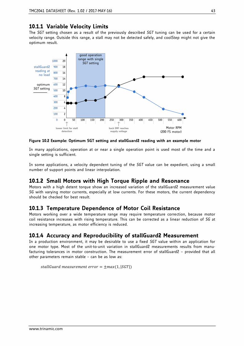
TMC2041 DATASHEET (Rev. 1.02 / 2017-MAY-16) 43
www.trinamic.com
10.1.1 Variable Velocity Limits The SGT setting chosen as a result of the previously described SGT tuning can be used for a certain velocity range. Outside this range, a stall may not be detected safely, and coolStep might not give the optimum result.
back EMF reaches supply voltage
optimum SGT setting
Motor RPM(200 FS motor)
stallGuard2 reading at
no load
2
4
6
8
10
12
14
16
100
200
300
400
500
600
700
800
900
1000
18
20
0 0 50 100 150 200 250 300 350 400 450 500 550 600
lower limit for stall detection
good operation range with single
SGT setting
Figure 10.2 Example: Optimum SGT setting and stallGuard2 reading with an example motor
In many applications, operation at or near a single operation point is used most of the time and a single setting is sufficient. In some applications, a velocity dependent tuning of the SGT value can be expedient, using a small number of support points and linear interpolation.
10.1.2 Small Motors with High Torque Ripple and Resonance Motors with a high detent torque show an increased variation of the stallGuard2 measurement value SG with varying motor currents, especially at low currents. For these motors, the current dependency should be checked for best result.
10.1.3 Temperature Dependence of Motor Coil Resistance Motors working over a wide temperature range may require temperature correction, because motor coil resistance increases with rising temperature. This can be corrected as a linear reduction of SG at increasing temperature, as motor efficiency is reduced.
10.1.4 Accuracy and Reproducibility of stallGuard2 Measurement In a production environment, it may be desirable to use a fixed SGT value within an application for one motor type. Most of the unit-to-unit variation in stallGuard2 measurements results from manu-facturing tolerances in motor construction. The measurement error of stallGuard2 – provided that all other parameters remain stable – can be as low as:
𝑠𝑡𝑎𝑙𝑙𝐺𝑢𝑎𝑟𝑑 𝑚𝑒𝑎𝑠𝑢𝑟𝑒𝑚𝑒𝑛𝑡 𝑒𝑟𝑟𝑜𝑟 = ±𝑚𝑎𝑥(1, |𝑆𝐺𝑇|)

TMC2041 DATASHEET (Rev. 1.02 / 2017-MAY-16) 44
www.trinamic.com
10.2 stallGuard2 Update Rate and Filter The stallGuard2 measurement value SG is updated with each full step of the motor. This is enough to safely detect a stall, because a stall always means the loss of four full steps. In a practical application, especially when using coolStep, a more precise measurement might be more important than an update for each fullstep because the mechanical load never changes instantaneously from one step to the next. For these applications, the sfilt bit enables a filtering function over four load measurements. The filter should always be enabled when high-precision measurement is required. It compensates for variations in motor construction, for example due to misalignment of the phase A to phase B magnets. The filter should be disabled when rapid response to increasing load is required and for best results of sensorless homing using stallGuard.
10.3 Detecting a Motor Stall For best stall detection, work without stallGuard filtering (sfilt=0). To safely detect a motor stall the stall threshold must be determined using a specific SGT setting. Therefore, the maximum load needs to be determined, which the motor can drive without stalling. At the same time, monitor the SG value at this load, e.g. some value within the range 0 to 100. The stall threshold should be a value safely within the operating limits, to allow for parameter stray. The response at an SGT setting at or near 0 gives some idea on the quality of the signal: Check the SG value without load and with maximum load. They should show a difference of at least 100 or a few 100, which shall be large compared to the offset. If you set the SGT value in a way, that a reading of 0 occurs at maximum motor load, the stall can be automatically detected by the motion controller to issue a motor stop. In the moment of the step resulting in a step loss, the lowest reading will be visible. After the step loss, the motor will vibrate and show a higher SG reading.
10.4 Homing with stallGuard The homing of a linear drive requires moving the motor into the direction of a hard stop. As stallGuard needs a certain velocity to work, make sure that the start point is far enough away from the hard stop to provide the distance required for the acceleration phase. After setting up SGT, start a motion into the direction of the hard stop and check SG for reaching 0.
10.5 Limits of stallGuard2 Operation stallGuard2 does not operate reliably at extreme motor velocities: Very low motor velocities (for many motors, less than one revolution per second) generate a low back EMF and make the measurement unstable and dependent on environment conditions (temperature, etc.). The automatic tuning procedure described above will compensate for this. Other conditions will also lead to extreme settings of SGT and poor response of the measurement value SG to the motor load. Very high motor velocities, in which the full sinusoidal current is not driven into the motor coils also leads to poor response. These velocities are typically characterized by the motor back EMF reaching the supply voltage.

TMC2041 DATASHEET (Rev. 1.02 / 2017-MAY-16) 45
www.trinamic.com
11 coolStep Operation coolStep is an automatic smart energy optimization for stepper motors based on the motor mechanical load, making them “green”.
11.1 User Benefits
coolStep allows substantial energy savings, especially for motors which see varying loads or operate at a high duty cycle. Because a stepper motor application needs to work with a torque reserve of 30% to 50%, even a constant-load application allows significant energy savings because coolStep automatically enables torque reserve when required. Reducing power consumption keeps the system cooler, increases motor life, and allows reducing cost in the power supply and cooling components.
Reducing motor current by half results in reducing power by a factor of four.
11.2 Setting up for coolStep coolStep is controlled by several parameters, but two are critical for understanding how it works:
Parameter Description Range Comment
SEMIN 4-bit unsigned integer that sets a lower threshold. If SG goes below this threshold, coolStep increases the current to both coils. The 4-bit SEMIN value is scaled by 32 to cover the lower half of the range of the 10-bit SG value. (The name of this parameter is derived from smartEnergy, which is an earlier name for coolStep.)
0 disable coolStep
1…15 threshold is SEMIN*32
SEMAX 4-bit unsigned integer that controls an upper threshold. If SG is sampled equal to or above this threshold enough times, coolStep decreases the current to both coils. The upper threshold is (SEMIN + SEMAX + 1)*32.
0…15 threshold is (SEMIN+SEMAX+1)*32
Figure 11.1 shows the operating regions of coolStep:
- The black line represents the SG measurement value.
- The blue line represents the mechanical load applied to the motor.
- The red line represents the current into the motor coils.
When the load increases, SG falls below SEMIN, and coolStep increases the current. When the load decreases, SG rises above (SEMIN + SEMAX + 1) * 32, and the current is reduced.
Energy efficiency – consumption decreased up to 75% Motor generates less heat – improved mechanical precision Less cooling infrastructure – for motor and driver Cheaper motor – does the job!

TMC2041 DATASHEET (Rev. 1.02 / 2017-MAY-16) 46
www.trinamic.com
stal
lGuar
d2
read
ing
0=maximum load
motor current increment area
motor current reduction area
stall possible
SEMIN
SEMAX+SEMIN+1
Zeit
moto
r cu
rrent
current setting I_RUN (upper limit)
½ or ¼ I_RUN (lower limit)
mech
anical
load
current in
crem
ent due to
incr
eas
ed load
slow
current re
duct
ion d
ue
to reduce
d m
oto
r lo
ad
load angle optimized load angle optimizedload angle
optimized
Figure 11.1 coolStep adapts motor current to the load
Five more parameters control coolStep and one status value is returned:
Parameter Description Range Comment
SEUP Sets the current increment step. The current becomes incremented for each measured stallGuard2 value below the lower threshold.
0…3 step width is 1, 2, 4, 8
SEDN Sets the number of stallGuard2 readings above the upper threshold necessary for each current decrement of the motor current.
0…3 number of stallGuard2 measurements per decrement: 32, 8, 2, 1
SEIMIN Sets the lower motor current limit for coolStep operation by scaling the IRUN current setting.
0 0: 1/2 of IRUN
1 1: 1/4 of IRUN
Status word
Description Range Comment
CSACTUAL This status value provides the actual motor current scale as controlled by coolStep. The value goes up to the IRUN value and down to the portion of IRUN as specified by SEIMIN.
0…31 1/32, 2/32, … 32/32

TMC2041 DATASHEET (Rev. 1.02 / 2017-MAY-16) 47
www.trinamic.com
11.3 Tuning coolStep Before tuning coolStep, first tune the stallGuard2 threshold level SGT, which affects the range of the load measurement value SG. coolStep uses SG to operate the motor near the optimum load angle of +90°. The current increment speed is specified in SEUP, and the current decrement speed is specified in SEDN. They can be tuned separately because they are triggered by different events that may need different responses. The encodings for these parameters allow the coil currents to be increased much more quickly than decreased, because crossing the lower threshold is a more serious event that may require a faster response. If the response is too slow, the motor may stall. In contrast, a slow response to crossing the upper threshold does not risk anything more serious than missing an opportunity to save power.
coolStep operates between limits controlled by the current scale parameter IRUN and the seimin bit.
11.3.1 Response Time For fast response to increasing motor load, use a high current increment step SEUP. If the motor load changes slowly, a lower current increment step can be used to avoid motor oscillations. If the filter controlled by sfilt is enabled, the measurement rate and regulation speed are cut by a factor of four.
Hint The most common and most beneficial use is to adapt coolStep for operation at the typical system target operation velocity and to set the velocity thresholds according. As acceleration and decelerations normally shall be quick, they will require the full motor current, while they have only a small contribution to overall power consumption due to their short duration.
11.3.2 Low Velocity and Standby Operation Because coolStep is not able to measure the motor load in standstill and at very low RPM, a lower velocity threshold is provided in the ramp generator. It should be set to an application specific default value. Below this threshold the normal current setting via IRUN respectively IHOLD is valid. An upper threshold is provided by the VHIGH setting. Both thresholds can be set as a result of the stallGuard2 tuning process.

TMC2041 DATASHEET (Rev. 1.02 / 2017-MAY-16) 48
www.trinamic.com
12 Step/Dir Interface The STEP and DIR inputs provide a simple, standard interface compatible with many existing motion controllers. The microPlyer STEP pulse interpolator brings the smooth motor operation of high-resolution microstepping to applications originally designed for coarser stepping. The current settings are configured separately for motor run and standstill in register IHOLD_IRUN.
12.1 Timing Figure 12.1 shows the timing parameters for the STEP and DIR signals, and the table below gives their specifications. When the DEDGE mode bit in the DRVCTRL register is set, both edges of STEP are active. If DEDGE is cleared, only rising edges are active. STEP and DIR are sampled and synchronized to the system clock. An internal analog filter removes glitches on the signals, such as those caused by long PCB traces. If the signal source is far from the chip, and especially if the signals are carried on cables, the signals should be filtered or differentially transmitted.
+VCC_IO
SchmittTrigger
0.44 VCC_IO
0.56 VCC_IO250k
0.26pF
Input filter
R*C = 65ns +-30%
STEP
or DIR
Input
Internal
Signal
DIR
STEP
tDSHtSH tSLtDSU
Activ
e e
dg
e
(DE
DG
E=
0)
Activ
e e
dg
e
(DE
DG
E=
0)
Figure 12.1 STEP and DIR timing, Input pin filter
STEP and DIR interface timing AC-Characteristics
clock period is tCLK
Parameter Symbol Conditions Min Typ Max Unit
step frequency (at maximum microstep resolution)
fSTEP dedge=0 ½ fCLK
dedge=1 ¼ fCLK
fullstep frequency fFS fCLK/512
STEP input low time *) tSL max(tFILTSD, tCLK+20)
ns
STEP input high time *) tSH max(tFILTSD,
tCLK+20) ns
DIR to STEP setup time tDSU 20 ns
DIR after STEP hold time tDSH 20 ns
STEP and DIR spike filtering time *)
tFILTSD rising and falling edge
36 60 85 ns
STEP and DIR sampling relative to rising CLK input
tSDCLKHI before rising edge of CLK input
tFILTSD ns
*) These values are valid with full input logic level swing, only. Asymmetric logic levels will increase filtering delay tFILTSD, due to an internal input RC filter.
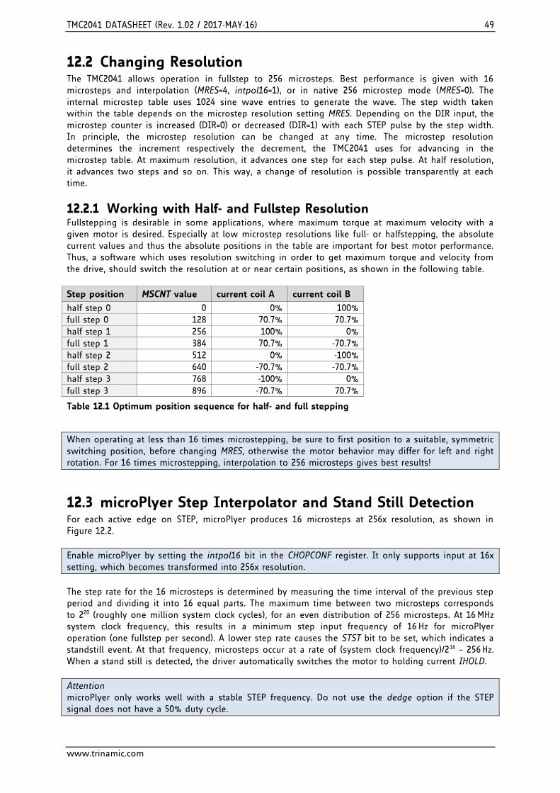
TMC2041 DATASHEET (Rev. 1.02 / 2017-MAY-16) 49
www.trinamic.com
12.2 Changing Resolution The TMC2041 allows operation in fullstep to 256 microsteps. Best performance is given with 16 microsteps and interpolation (MRES=4, intpol16=1), or in native 256 microstep mode (MRES=0). The internal microstep table uses 1024 sine wave entries to generate the wave. The step width taken within the table depends on the microstep resolution setting MRES. Depending on the DIR input, the microstep counter is increased (DIR=0) or decreased (DIR=1) with each STEP pulse by the step width. In principle, the microstep resolution can be changed at any time. The microstep resolution determines the increment respectively the decrement, the TMC2041 uses for advancing in the microstep table. At maximum resolution, it advances one step for each step pulse. At half resolution, it advances two steps and so on. This way, a change of resolution is possible transparently at each time.
12.2.1 Working with Half- and Fullstep Resolution Fullstepping is desirable in some applications, where maximum torque at maximum velocity with a given motor is desired. Especially at low microstep resolutions like full- or halfstepping, the absolute current values and thus the absolute positions in the table are important for best motor performance. Thus, a software which uses resolution switching in order to get maximum torque and velocity from the drive, should switch the resolution at or near certain positions, as shown in the following table.
Step position MSCNT value current coil A current coil B
half step 0 0 0% 100%
full step 0 128 70.7% 70.7%
half step 1 256 100% 0%
full step 1 384 70.7% -70.7%
half step 2 512 0% -100%
full step 2 640 -70.7% -70.7%
half step 3 768 -100% 0%
full step 3 896 -70.7% 70.7%
Table 12.1 Optimum position sequence for half- and full stepping
When operating at less than 16 times microstepping, be sure to first position to a suitable, symmetric switching position, before changing MRES, otherwise the motor behavior may differ for left and right rotation. For 16 times microstepping, interpolation to 256 microsteps gives best results!
12.3 microPlyer Step Interpolator and Stand Still Detection For each active edge on STEP, microPlyer produces 16 microsteps at 256x resolution, as shown in Figure 12.2.
Enable microPlyer by setting the intpol16 bit in the CHOPCONF register. It only supports input at 16x setting, which becomes transformed into 256x resolution.
The step rate for the 16 microsteps is determined by measuring the time interval of the previous step period and dividing it into 16 equal parts. The maximum time between two microsteps corresponds to 220 (roughly one million system clock cycles), for an even distribution of 256 microsteps. At 16 MHz system clock frequency, this results in a minimum step input frequency of 16 Hz for microPlyer operation (one fullstep per second). A lower step rate causes the STST bit to be set, which indicates a standstill event. At that frequency, microsteps occur at a rate of (system clock frequency)/216 ~ 256 Hz. When a stand still is detected, the driver automatically switches the motor to holding current IHOLD.
Attention microPlyer only works well with a stable STEP frequency. Do not use the dedge option if the STEP signal does not have a 50% duty cycle.

TMC2041 DATASHEET (Rev. 1.02 / 2017-MAY-16) 50
www.trinamic.com
STEP
Interpolated microstep
Act
ive e
dge
(ded
ge=
0)
Act
ive e
dge
(ded
ge=
0)
Act
ive e
dge
(ded
ge=
0)
0 1 2 3 4 5 6 7 8 9 10 11 12 13 14 15 16 17 18 19 20 21 22 23 32
Act
ive e
dge
(ded
ge=
0)
STANDSTILL (stst) active
33 34 35 36 37 38 39 40 41 42 43 44 45 46 47 48 49 50
Motorangle
52 53 54 55 56 57 58 59 60 61 62 63 64 65 6651
2^20 tCLK
Figure 12.2 microPlyer microstep interpolation with rising STEP frequency
In Figure 12.2, the first STEP cycle is long enough to set the standstill bit stst. This bit is cleared on the next STEP active edge. Then, the external STEP frequency increases. After one cycle at the higher rate microPlyer adapts the interpolated microstep rate to the higher frequency. During the last cycle at the slower rate, microPlyer did not generate all 16 microsteps, so there is a small jump in motor angle between the first and second cycles at the higher rate.
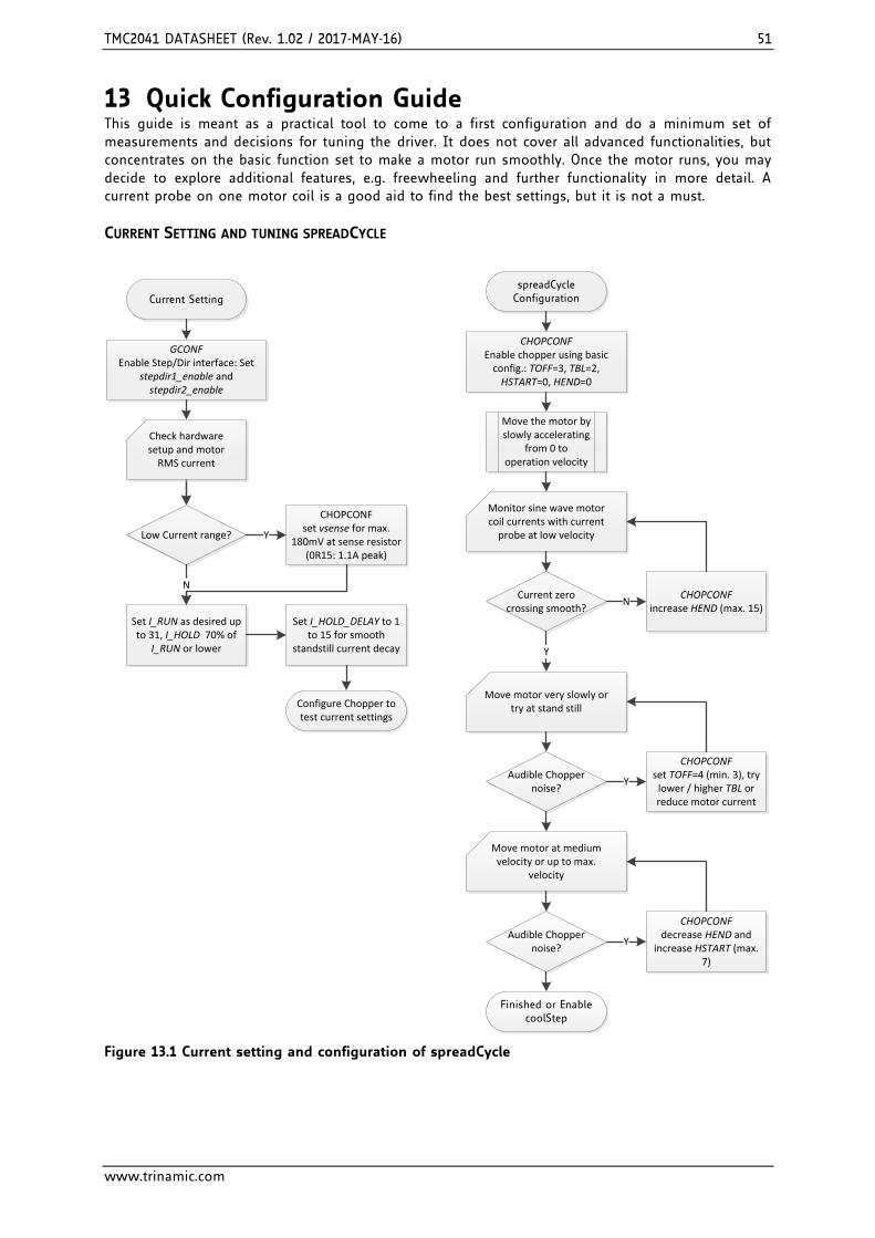
TMC2041 DATASHEET (Rev. 1.02 / 2017-MAY-16) 51
www.trinamic.com
13 Quick Configuration Guide This guide is meant as a practical tool to come to a first configuration and do a minimum set of measurements and decisions for tuning the driver. It does not cover all advanced functionalities, but concentrates on the basic function set to make a motor run smoothly. Once the motor runs, you may decide to explore additional features, e.g. freewheeling and further functionality in more detail. A current probe on one motor coil is a good aid to find the best settings, but it is not a must.
CURRENT SETTING AND TUNING SPREADCYCLE
Current Setting
CHOPCONFset vsense for max.
180mV at sense resistor (0R15: 1.1A peak)
Set I_RUN as desired up to 31, I_HOLD 70% of
I_RUN or lower
Low Current range?
N
Y
Set I_HOLD_DELAY to 1 to 15 for smooth
standstill current decay
Configure Chopper to test current settings
Check hardware setup and motor
RMS current
spreadCycle Configuration
CHOPCONFEnable chopper using basic
config.: TOFF=3, TBL=2, HSTART=0, HEND=0
Move the motor by slowly accelerating
from 0 to operation velocity
Monitor sine wave motor coil currents with current
probe at low velocity
CHOPCONFincrease HEND (max. 15)
Current zero crossing smooth?
N
Move motor very slowly or try at stand still
CHOPCONFset TOFF=4 (min. 3), try
lower / higher TBL or reduce motor current
Audible Chopper noise?
Y
Y
Move motor at medium velocity or up to max.
velocity
Audible Chopper noise?
CHOPCONFdecrease HEND and
increase HSTART (max. 7)
Y
Finished or Enable coolStep
GCONFEnable Step/Dir interface: Set
stepdir1_enable and stepdir2_enable
Figure 13.1 Current setting and configuration of spreadCycle

TMC2041 DATASHEET (Rev. 1.02 / 2017-MAY-16) 52
www.trinamic.com
ENABLING COOLSTEP (ONLY IN COMBINATION WITH SPREADCYCLE)
Enable coolStep
Move the motor by slowly accelerating from 0 to operation velocity V
Does SG_RESULT go down to 0 with load?
Monitor SG_RESULT value during medium velocity and
check response with mechanical load
Is coil current sine-shaped at V?
Decrease VN
Y
Increase SGTY
COOLCONFEnable coolStep basic config.:
SEMIN=1, all other 0
N
Set VCOOLTHRSto the lower velocity
limit for coolStep
Monitor CS_ACTUAL during motion in velocity range and check response with
mechanical load
Does CS_ACTUAL reach IRUN with load before
motor stall?
Increase SEMIN or choose narrower
velocity limitsN
C2
C2
Monitor CS_ACTUAL and motor torque during rapid mechanical load increment
within application limits
Does CS_ACTUAL reach IRUN with load before
motor stall?Increase SEUPN
Finished
Figure 13.2 Enabling coolStep (only in combination with spreadCycle)

TMC2041 DATASHEET (Rev. 1.02 / 2017-MAY-16) 53
www.trinamic.com
14 Getting Started Please refer to the TMC2041 evaluation board to allow a quick start with the device, and in order to allow interactive tuning of the device setup in your application. Alternatively, all tuning can be done using a TMC5072 evaluation board, as the TMC5072 driver part is fully compatible. Chapter 13 will guide you through the process of correctly setting up all registers.
14.1 Initialization Examples Initialization SPI datagram example sequence to enable driver 1 for step and direction operation and initialize the chopper for a 2 phase motor:
SPI send: 0x8000000006; // GCONF=6: Enable both drivers for step and direction operation SPI send: 0xEC000100C3; // CHOPCONF: TOFF=3, HSTRT=4, HEND=1, TBL=2, CHM=0 (spreadCycle) SPI send: 0xB000061F05; // IHOLD_IRUN: IHOLD=5, IRUN=31 (max. current), IHOLDDELAY=6
For UART based operation it is important to make sure that the CRC byte is correct. The following example shows initialization for a TMC2041 with slave address 0 (NEXTADDR pin low). It programs driver 1 and driver 2 to spreadCycle mode:
UART write: 0x05 0x00 0x80 0x00 0x00 0x00 0x06 0x6E; // stepdir1=1, stepdir2=1 UART write: 0x05 0x00 0xEC 0x00 0x01 0x00 0xC5 0xD3; // DRV1: TOFF=5, HEND=1, HSTR=4, // TBL=2, MRES=0, CHM=0 UART write: 0x05 0x00 0xB0 0x00 0x01 0x14 0x05 0xBB; // IHOLD=5, IRUN=20, IHOLDDELAY=1 UART write: 0x05 0x00 0xFC 0x00 0x01 0x00 0xC5 0x01; // DRV2: TOFF=5, HEND=1, HSTR=4, // TBL=2, MRES=0, CHM=0 UART write: 0x05 0x00 0xD0 0x00 0x01 0x14 0x05 0xF0; // IHOLD=5, IRUN=20, IHOLDDELAY=1
UART read: 0x05 0x00 0x01 0xC1; // Request driver status GSTAT
Hint Tune the configuration parameters for your motor and application for optimum performance. For generation of the UART data, use the CRC calculation tool from www.trinamic.com.

TMC2041 DATASHEET (Rev. 1.02 / 2017-MAY-16) 54
www.trinamic.com
15 External Reset The chip is loaded with default values during power on via its internal power-on reset. In order to reset the chip to power on defaults, any of the supply voltages monitored by internal reset circuitry (VSA, +5VOUT or VCC_IO) must be cycled. VCC is not monitored. Therefore VCC must not be switched off during operation of the chip. As +5VOUT is the output of the internal voltage regulator, it cannot be cycled via an external source except by cycling VSA. It is easiest and safest to cycle VCC_IO in order to completely reset the chip. Also, current consumed from VCC_IO is low and therefore it has simple driving requirements. Due to the input protection diodes not allowing the digital inputs to rise above VCC_IO level, all inputs must be driven low during this reset operation. When this is not possible, an input protection resistor may be used to limit current flowing into the related inputs. In case, VCC becomes supplied by an external source, make sure that VCC is at a stable value above the lower operation limit once the reset ends. This normally is satisfied when generating a 3.3V VCC_IO from the +5V supply supplying the VCC pin, because it will then come up with a certain delay.
16 Clock Oscillator and Clock Input The clock is the timing reference for the chopper operation. As the actual chopper frequency normally is less critical, the internal clock oscillator can be used for most cases.
16.1 Using the Internal Clock Directly tie the CLK input to GND near to the TMC2041 if the internal clock oscillator is to be used. The temperature dependency and ageing of the internal clock is comparatively low.
Hint In case precise motor chopper operation and best stability of stallGuard are desired, it is supposed to work with an external clock source.
16.2 Using an External Clock When an external clock is available, a frequency of 10 MHz to 16 MHz is recommended for optimum performance. The duty cycle of the clock signal is uncritical, as long as minimum high or low input time for the pin is satisfied (refer to electrical characteristics). Up to 18 MHz can be used, when the clock duty cycle is 50%. Make sure, that the clock source supplies clean CMOS output logic levels and steep slopes when using a high clock frequency. The external clock input is enabled with the first positive polarity seen on the CLK input.
Attention Switching off the external clock frequency prevents the driver from operating normally. Therefore be careful to switch off the motor drivers before switching off the clock (e.g. using the enable input), because otherwise the chopper would stop and the motor current level could rise uncontrolled. The short to GND detection stays active even without clock, if enabled.
16.3 Considerations on the Frequency A higher frequency allows faster step rates, faster SPI operation and higher chopper frequencies. On the other hand, it may cause more electromagnetic emission of the system and causes more power dissipation in the TMC2041 digital core and voltage regulator. Generally a frequency of 10 MHz to 16 MHz should be sufficient for most applications. For reduced requirements concerning the motor dynamics, a clock frequency of down to 8 MHz can be considered.

TMC2041 DATASHEET (Rev. 1.02 / 2017-MAY-16) 55
www.trinamic.com
17 Absolute Maximum Ratings The maximum ratings may not be exceeded under any circumstances. Operating the circuit at or near more than one maximum rating at a time for extended periods shall be avoided by application design.
Parameter Symbol Min Max Unit
Supply voltage operating with inductive load (VVS ≥ VVSA) VVS, VVSA -0.5 27 V
Supply and bridge voltage max. *) VVS -0.5 28 V
VSA when different from to VS VVSA -0.5 VVS+0.5 V
I/O supply voltage VVIO -0.5 5.5 V
digital VCC supply voltage (if not supplied by internal regulator)
VVCC -0.5 5.5 V
Logic input voltage VI -0.5 VVIO+0.5 V
Maximum current to / from digital pins and analog low voltage I/Os
IIO +/-10 mA
5V regulator output current (internal plus external load) I5VOUT 50 mA
5V regulator continuous power dissipation (VVM-5V) * I5VOUT P5VOUT 1 W
Power bridge repetitive output current IOx 2.0 A
Junction temperature TJ -50 150 °C
Storage temperature TSTG -55 150 °C
ESD-Protection for interface pins (Human body model, HBM)
VESDAP 4 (tbd.) kV
ESD-Protection for handling (Human body model, HBM) VESD 1 (tbd.) kV
*) Stray inductivity of GND and VS connections will lead to ringing of the supply voltage when driving an inductive load. This ringing results from the fast switching slopes of the driver outputs in combination with reverse recovery of the body diodes of the output driver MOSFETs. Even small trace inductivities as well as stray inductivity of sense resistors can easily generate a few volts of ringing leading to temporary voltage overshoot. This should be considered when working near the maximum voltage.
18 Electrical Characteristics
18.1 Operational Range Parameter Symbol Min Max Unit
Junction temperature TJ -40 125 °C
Supply voltage (using internal +5V regulator) VVS 5.5 26 V
Supply voltage (internal +5V regulator bridged: VVCC=VVSA) VVS 4.7 5.4 V
I/O supply voltage VVIO 3.00 5.25 V
VCC voltage when using optional external source (supplies digital logic and charge pump)
VVCC 4.6 5.25 V
RMS motor coil current per coil (value for design guideline) IRMS 0.8 A
Peak output current per motor coil output (sine wave peak) IOx 1.1 A
Peak output current per motor coil output (sine wave peak) Limit TJ ≤ 105°C, e.g. for 100ms short time acceleration phase below 50% duty cycle.
IOx 1.5 A

TMC2041 DATASHEET (Rev. 1.02 / 2017-MAY-16) 56
www.trinamic.com
18.2 DC Characteristics and Timing Characteristics DC characteristics contain the spread of values guaranteed within the specified supply voltage range unless otherwise specified. Typical values represent the average value of all parts measured at +25°C. Temperature variation also causes stray to some values. A device with typical values will not leave Min/Max range within the full temperature range.
Power supply current DC-Characteristics
VVS = 24.0V
Parameter Symbol Conditions Min Typ Max Unit
Total supply current, driver disabled IVS + IVSA + IVCC
IS fCLK=16MHz 25 40 mA
Total supply current, operating, IVS + IVSA + IVCC
IS fCLK=16MHz, 40kHz chopper
28 mA
Static supply current IVS0 fCLK=0Hz 3 4.5 7 mA
Supply current, driver disabled, dependency on CLK frequency
IVSX fCLK variable, additional to IVS0
1.3
mA/MHz
Internal current consumption from 5V supply on VCC pin
IVCC fCLK=16MHz, 40kHz chopper
25 40 mA
IO supply current IVIO no load on outputs, inputs at VIO or GND
15 30 µA
Motor driver section DC- and Timing-Characteristics
VVS = 24.0V
Parameter Symbol Conditions Min Typ Max Unit
RDSON lowside MOSFET RONL measure at 100mA, 25°C, static state
0.4 0.5 Ω
RDSON highside MOSFET RONH measure at 100mA, 25°C, static state
0.5 0.6 Ω
slope, MOSFET turning on tSLPON measured at 700mA load current
50 120 250 ns
slope, MOSFET turning off tSLPOFF measured at 700mA load current
50 220 450 ns
Current sourcing, driver off IOIDLE OXX pulled to GND 120 180 250 µA
Charge pump DC-Characteristics
Parameter Symbol Conditions Min Typ Max Unit
Charge pump output voltage VVCP-VVS operating, typical fchop<40kHz
4.0 V5VOUT -0.4
V5VOUT V
Charge pump voltage threshold for undervoltage detection
VVCP-VVS using internal 5V regulator voltage
3.1 3.6 3.9 V
Charge pump frequency fCP 1/16 fCLKOSC
Linear regulator DC-Characteristics
Parameter Symbol Conditions Min Typ Max Unit
Output voltage V5VOUT I5VOUT = 0mA
TJ = 25°C
4.75 5.0 5.25 V
Output resistance R5VOUT Static load 3
Deviation of output voltage over the full temperature range
V5VOUT(DEV) I5VOUT = 30mA
TJ = full range
30 100 mV
TMC2041 DATASHEET (Rev. 1.02 / 2017-MAY-16) 57
www.trinamic.com
Clock oscillator and input Timing-Characteristics
Parameter Symbol Conditions Min Typ Max Unit
Clock oscillator frequency fCLKOSC tJ=-50°C 9 12.4 MHz
Clock oscillator frequency fCLKOSC tJ=50°C 10.1 13.2 17.2 MHz
Clock oscillator frequency fCLKOSC tJ=150°C 13.4 18 MHz
External clock frequency (operating)
fCLK 4 10-16 18 MHz
External clock high / low level time
tCLKL / tCLKH CLK driven to 0.1 VVIO / 0.9 VVIO
10 ns
External clock first cycle triggering switching to external clock source
tCLK1 CLK driven high 30 25 ns
Detector levels DC-Characteristics
Parameter Symbol Conditions Min Typ Max Unit
VVSA undervoltage threshold for RESET
VUV_VSA VVS rising 3.8 4.2 4.6 V
V5VOUT undervoltage threshold for RESET
VUV_5VOUT V5VOUT rising 3.5 V
VVCC_IO undervoltage threshold for RESET
VUV_VIO VVCC_IO rising 1.9 2.55 3.0 V
VVCC_IO undervoltage detector hysteresis
VUV_VIOHYST 0.1 0.3 0.5 V
Short to GND detector threshold (VVSP - VOx)
VOS2G 1.5 2.2 3 V
Short to GND detector delay (high side switch on to short detected)
tS2G High side output clamped to VSP-3V
0.8 1.3 2 µs
Overtemperature prewarning tOTPW Temperature rising 100 120 140 °C
Overtemperature shutdown tOT Temperature rising 135 150 170 °C
Sense resistor voltage levels DC-Characteristics
Parameter Symbol Conditions Min Typ Max Unit
Sense input peak threshold voltage (low sensitivity)
VSRTL vsense=0 csactual=31 sin_x=248 Hyst.=0; IBRxy=0
320 mV
sense input peak threshold voltage (high sensitivity)
VSRTH vsense=1 csactual=31 sin_x=248 Hyst.=0; IBRxy=0
180 mV
Sense input tolerance / motor current full scale tolerance
ICOIL vsense=0 -5 +5 %
Internal resistance from pin BRxy to internal sense comparator (additional to sense resistor)
RBRxy 20 mΩ
TMC2041 DATASHEET (Rev. 1.02 / 2017-MAY-16) 58
www.trinamic.com
Digital logic levels DC-Characteristics
Parameter Symbol Conditions Min Typ Max Unit
Input voltage low level VINLO -0.3 0.3 VVIO V
Input voltage high level VINHI 0.7 VVIO VVIO+0.3 V
Input Schmitt trigger hysteresis VINHYST 0.12 VVIO
V
Output voltage low level VOUTLO IOUTLO = 2mA 0.2 V
Output voltage high level VOUTHI IOUTHI = -2mA VVIO-0.2 V
Input leakage current IILEAK -10 10 µA
Digital pin capacitance C 3.5 pF

TMC2041 DATASHEET (Rev. 1.02 / 2017-MAY-16) 59
www.trinamic.com
18.3 Thermal Characteristics The following table shall give an idea on the thermal resistance of the QFN-48 package. The thermal resistance for a four layer board will provide a good idea on a typical application. The single layer board example is kind of a worst case condition, as the typical application will require a 4 layer board. Actual thermal characteristics will depend on the PCB layout, PCB type and PCB size. A thermal resistance of 23°C/W for a typical board means, that the package is capable of continuously dissipating 4W at an ambient temperature of 25°C with the die temperature staying below 125°C.
Parameter Symbol Conditions Typ Unit
Typical power dissipation
One motor active, one motor in standby at low current
PD One motor 1.00A RMS 115°C (125°C)
One motor 0.71A RMS 85°C (93°C)
Surface temperature at package center (peak surface temperature), board 55mm x 85mm, 25°C environment
spreadCycle, sinewave, 40 or 20kHz chopper, 24V, 16MHz, internal supply for VCC
Motors: QSH4218-035-10-027
3.7
2.4
W
W
Typical power dissipation
Two motors active
PD Two motors 0.71A RMS 113°C (119°C)
Two motors 0.35A RMS 64°C (68°C)
3.7
1.4
W
W
Thermal resistance junction to ambient on a single layer board
RTJA Single signal layer board (1s) as defined in JEDEC EIA JESD51-3 (FR4, 76.2mm x 114.3mm, d=1.6mm)
80 K/W
Thermal resistance junction to ambient on a multilayer board
RTMJA Dual signal and two internal power plane board (2s2p) as defined in JEDEC EIA JESD51-5 and JESD51-7 (FR4, 76.2mm x 114.3mm, d=1.6mm)
23 K/W
Thermal resistance junction to ambient on a multilayer board with air flow
RTMJA1 Identical to RTMJA, but with air flow 1m/s
20 K/W
Thermal resistance junction to board
RTJB PCB temperature measured within 1mm distance to the package
10 K/W
Thermal resistance junction to case
RTJC Junction temperature to heat slug of package
3 K/W
The thermal resistance in an actual layout can be tested by checking for the heat up caused by the standby power consumption of the chip. When no motor is attached, all power seen on the power supply is dissipated within the chip.
Note A spread-sheet for calculating TMC2041 power dissipation is available on www.trinamic.com.

TMC2041 DATASHEET (Rev. 1.02 / 2017-MAY-16) 60
www.trinamic.com
19 Layout Considerations
19.1 Exposed Die Pad The TMC2041 uses its die attach pad to dissipate heat from the drivers and the linear regulator to the board. For best electrical and thermal performance, use a reasonable amount of solid, thermally conducting vias between the die attach pad and the ground plane. The printed circuit board should have a solid ground plane spreading heat into the board and providing for a stable GND reference.
19.2 Wiring GND All signals of the TMC2041 are referenced to their respective GND. Directly connect all GND pins under the TMC2041 to a common ground area (GND, GNDP, GNDA and die attach pad). The GND plane right below the die attach pad should be treated as a virtual star point. For thermal reasons, the PCB top layer shall be connected to a large PCB GND plane spreading heat within the PCB.
Attention Especially, the sense resistors are susceptible to GND differences and GND ripple voltage, as the microstep current steps make up for voltages down to 0.5 mV. No current other than the sense resistor current should flow on their connections to GND and to the TMC2041. Optimally place them close to the TMC2041, with one or more vias to the GND plane for each sense resistor. The two sense resistors for one coil should not share a common ground connection trace or vias, as also PCB traces have a certain resistance.
19.3 Supply Filtering The 5VOUT output voltage ceramic filtering capacitor (4.7 µF recommended) should be placed as close as possible to the 5VOUT pin, with its GND return going directly to the GNDA pin. Use as short and as thick connections as possible. For best microstepping performance and lowest chopper noise an additional filtering capacitor can be used for the VCC pin to GND, to avoid charge pump and digital part ripple influencing motor current regulation. Therefore place a ceramic filtering capacitor (470nF recommended) as close as possible (1-2mm distance) to the VCC pin with GND return going to the ground plane. VCC can be coupled to 5VOUT using a 2.2 Ω resistor in order to supply the digital logic from 5VOUT while keeping ripple away from this pin. A 100 nF filtering capacitor should be placed as close as possible to the VSA pin to ground plane. The motor supply pins VS should be decoupled with an electrolytic capacitor (47 μF or larger is recommended) and a ceramic capacitor, placed close to the device. Take into account that the switching motor coil outputs have a high dV/dt. Thus capacitive stray into high resistive signals can occur, if the motor traces are near other traces over longer distances.
19.4 Single Driver Connection In a parallel connection setup, where the TMC2041 drives one motor with double current, take into account, that driver 1 takes over the complete control. Thus, the driver 1 layout should be optimized concerning sense resistor placement, etc. Connect driver 2 bridge outputs and BR pins in parallel to the corresponding driver 1 pins. Especially for the BR pins of driver 2, it is important to use low inductivity interconnection lines to driver 1.

TMC2041 DATASHEET (Rev. 1.02 / 2017-MAY-16) 61
www.trinamic.com
19.5 Layout Example
Schematic
1- Top Layer (assembly side)
2- Inner Layer (GND)
3- Inner Layer (supply VS)
4- Bottom Layer
Components
Figure 19.1 Layout example

TMC2041 DATASHEET (Rev. 1.02 / 2017-MAY-16) 62
www.trinamic.com
20 Package Mechanical Data
20.1 Dimensional Drawings Attention: Drawings not to scale.
Figure 20.1 Dimensional drawings
Parameter [mm] Ref Min Nom Max
total thickness A 0.80 0.85 0.90
stand off A1 0.00 0.035 0.05
mold thickness A2 - 0.65 0.67
lead frame thickness A3 0.203
lead width b 0.2 0.25 0.3
body size X D 7.0
body size Y E 7.0
lead pitch e 0.5
exposed die pad size X J 5.2 5.3 5.4
exposed die pad size Y K 5.2 5.3 5.4
lead length L 0.35 0.4 0.45
package edge tolerance aaa 0.1
mold flatness bbb 0.1
coplanarity ccc 0.08
lead offset ddd 0.1
exposed pad offset eee 0.1
20.2 Package Codes
Type Package Temperature range Code & marking
TMC2041-LA QFN48 (RoHS) -40°C ... +125°C TMC2041-LA

TMC2041 DATASHEET (Rev. 1.02 / 2017-MAY-16) 63
www.trinamic.com
21 Disclaimer TRINAMIC Motion Control GmbH & Co. KG does not authorize or warrant any of its products for use in life support systems, without the specific written consent of TRINAMIC Motion Control GmbH & Co. KG. Life support systems are equipment intended to support or sustain life, and whose failure to perform, when properly used in accordance with instructions provided, can be reasonably expected to result in personal injury or death. Information given in this data sheet is believed to be accurate and reliable. However no responsibility is assumed for the consequences of its use nor for any infringement of patents or other rights of third parties which may result from its use. Specifications are subject to change without notice. All trademarks used are property of their respective owners.
22 ESD Sensitive Device The TMC2041 is an ESD sensitive CMOS device sensitive to electrostatic discharge. Take special care to use adequate grounding of personnel and machines in manual handling. After soldering the devices to the board, ESD requirements are more relaxed. Failure to do so can result in defect or decreased reliability.
TMC2041 DATASHEET (Rev. 1.02 / 2017-MAY-16) 64
www.trinamic.com
23 Table of Figures Figure 1.1 Basic application and block diagram .......................................................................................................... 4 Figure 1.2 Energy efficiency with coolStep (example) ............................................................................................... 6 Figure 2.1 TMC2041 pin assignments. ............................................................................................................................. 7 Figure 3.1 Standard application circuit ......................................................................................................................... 10 Figure 3.2 5V only operation ........................................................................................................................................... 11 Figure 3.3 Driving a single motor with high current............................................................................................... 12 Figure 3.4 Using an external 5V supply to bypass internal regulator ................................................................ 13 Figure 3.5 RC-Filter on VCC for reduced ripple .......................................................................................................... 13 Figure 3.6 Simple ESD enhancement and more elaborate motor output protection .................................... 14 Figure 4.1 SPI timing ......................................................................................................................................................... 17 Figure 5.1 Addressing multiple TMC2041 via single wire interface using chaining ....................................... 21 Figure 5.2 Addressing multiple TMC2041 via differential interface, additional filtering for NEXTADDR ... 22 Figure 8.1 Chopper phases .............................................................................................................................................. 34 Figure 8.2 No ledges in current wave with sufficient hysteresis (magenta: current A, yellow & blue: sense resistor voltages A and B) ................................................................................................................................... 36 Figure 8.3 spreadCycle chopper scheme showing coil current during a chopper cycle ............................... 37 Figure 8.4 Classic const. off time chopper with offset showing coil current................................................... 38 Figure 8.5 Zero crossing with classic chopper and correction using sine wave offset................................. 38 Figure 10.1 Function principle of stallGuard2 ............................................................................................................ 41 Figure 10.2 Example: Optimum SGT setting and stallGuard2 reading with an example motor ................. 43 Figure 11.1 coolStep adapts motor current to the load ......................................................................................... 46 Figure 12.1 STEP and DIR timing, Input pin filter .................................................................................................... 48 Figure 12.2 microPlyer microstep interpolation with rising STEP frequency .................................................... 50 Figure 13.1 Current setting and configuration of spreadCycle.............................................................................. 51 Figure 13.3 Enabling coolStep (only in combination with spreadCycle) ............................................................ 52 Figure 19.1 Layout example ............................................................................................................................................. 61 Figure 20.1 Dimensional drawings ................................................................................................................................ 62

TMC2041 DATASHEET (Rev. 1.02 / 2017-MAY-16) 65
www.trinamic.com
24 Revision History
Version Date Author BD – Bernhard Dwersteg
Description
0.90 2016-NOV-23 BD First version based on TMC5072 datasheet
1.00 2016-NOV-25 BD Complete version
1.02 2017-MAY-16 BD Minor corrections
Table 24.1 Documentation revisions
25 References [TMC2041-EVAL] TMC2041-EVAL Manual [AN001] Trinamic Application Note 001 - Parameterization of spreadCycle™, www.trinamic.com [AN002] Trinamic Application Note 002 - Parameterization of stallGuard2™ & coolStep™,
www.trinamic.com Calculation sheet TMC50XX_Calculations.xlsx