Embed Size (px)
Citation preview
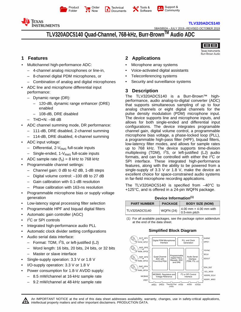
Audio Serial Interface
(TDM, I2S, LJ)
PLL and Clock
GenerationDigital PDM Microphones
Interface
I2C or SPI Control Interface
MICBIAS, Regulators and Voltage Reference
Programmable Digital Filters, Biquads, AGC
and DRE
Quad Channel ADC with
Front-End PGA
IN1P_GPI1
IN1M_GPO1
IN2P_GPI2
IN2M_GPO2
IN3P_GPI3
IN3M_GPO3
IN4P_GPI4
IN4M_GPO4
MICBIAS
VREF
FSYNC
BCLK
SDOUT
GPIO1
SHDNZ
SDA_SSZ
SCL_MOSI
ADDR0_SCLK
ADDR1_MISO
AREG DREG AVSSThermal Pad
(VSS)AVDD IOVDD
Product
Folder
Order
Now
Technical
Documents
Tools &
Software
Support &Community
An IMPORTANT NOTICE at the end of this data sheet addresses availability, warranty, changes, use in safety-critical applications,intellectual property matters and other important disclaimers. PRODUCTION DATA.
TLV320ADC5140SBAS892A –JULY 2019–REVISED OCTOBER 2019
TLV320ADC5140 Quad-Channel, 768-kHz, Burr-BrownTM Audio ADC
1
1 Features1• Multichannel high-performance ADC:
– 4-channel analog microphones or line-in,– 8-channel digital PDM microphones, or– Combination of analog and digital microphones
• ADC line and microphone differential inputperformance:– Dynamic range (DR):
– 120-dB, dynamic range enhancer (DRE)enabled
– 108-dB, DRE disabled– THD+N: –98 dB
• ADC channel summing mode, DR performance:– 111-dB, DRE disabled, 2-channel summing– 114-dB, DRE disabled, 4-channel summing
• ADC input voltage:– Differential, 2-VRMS full-scale inputs– Single-ended, 1-VRMS full-scale inputs
• ADC sample rate (fS) = 8 kHz to 768 kHz• Programmable channel settings:
– Channel gain: 0 dB to 42 dB, 1-dB steps– Digital volume control: –100 dB to 27 dB– Gain calibration with 0.1-dB resolution– Phase calibration with 163-ns resolution
• Programmable microphone bias or supply voltagegeneration
• Low-latency signal processing filter selection• Programmable HPF and biquad digital filters• Automatic gain controller (AGC)• I2C or SPI controls• Integrated high-performance audio PLL• Automatic clock divider setting configurations• Audio serial data interface:
– Format: TDM, I2S, or left-justified (LJ)– Word length: 16 bits, 20 bits, 24 bits, or 32 bits– Master or slave interface
• Single-supply operation: 3.3 V or 1.8 V• I/O-supply operation: 3.3 V or 1.8 V• Power consumption for 1.8-V AVDD supply:
– 8.5 mW/channel at 16-kHz sample rate– 9.2 mW/channel at 48-kHz sample rate
2 Applications• Microphone array systems• Voice-activated digital assistants• Teleconferencing systems• Security and surveillance systems
3 DescriptionThe TLV320ADC5140 is a Burr-Brown™ high-performance, audio analog-to-digital converter (ADC)that supports simultaneous sampling of up to fouranalog channels or eight digital channels for thepulse density modulation (PDM) microphone input.The device supports line and microphone inputs, andallows for both single-ended and differential inputconfigurations. The device integrates programablechannel gain, digital volume control, a programmablemicrophone bias voltage, a phase-locked loop (PLL),a programmable high-pass filter (HPF), biquad filters,low-latency filter modes, and allows for sample ratesup to 768 kHz. The device supports time-divisionmultiplexing (TDM), I2S, or left-justified (LJ) audioformats, and can be controlled with either the I2C orSPI interface. These integrated high-performancefeatures, along with the ability to be powered from asingle-supply of 3.3 V or 1.8 V, make the device anexcellent choice for space-constrained audio systemsin far-field microphone recording applications.
The TLV320ADC5140 is specified from –40°C to+125°C, and is offered in a 24-pin WQFN package.
Device Information(1)
PART NUMBER PACKAGE BODY SIZE (NOM)
TLV320ADC5140 WQFN (24) 4.00 mm × 4.00 mm with0.5-mm pitch
(1) For all available packages, see the package option addendumat the end of the data sheet.
Simplified Block Diagram
2
TLV320ADC5140SBAS892A –JULY 2019–REVISED OCTOBER 2019 www.ti.com
Product Folder Links: TLV320ADC5140
Submit Documentation Feedback Copyright © 2019, Texas Instruments Incorporated
Table of Contents1 Features .................................................................. 12 Applications ........................................................... 13 Description ............................................................. 14 Revision History..................................................... 25 Device Comparison Table ..................................... 36 Pin Configuration and Functions ......................... 47 Specifications......................................................... 6
7.1 Absolute Maximum Ratings ...................................... 67.2 ESD Ratings.............................................................. 67.3 Recommended Operating Conditions....................... 67.4 Thermal Information .................................................. 77.5 Electrical Characteristics........................................... 77.6 Timing Requirements: I2C Interface........................ 117.7 Switching Characteristics: I2C Interface.................. 117.8 Timing Requirements: SPI Interface ....................... 127.9 Switching Characteristics: SPI Interface ................. 127.10 Timing Requirements: TDM, I2S or LJ Interface... 127.11 Switching Characteristics: TDM, I2S or LJ
Interface ................................................................... 127.12 Timing Requirements: PDM Digital Microphone
Interface ................................................................... 137.13 Switching Characteristics: PDM Digial Microphone
Interface ................................................................... 137.14 Typical Characteristics .......................................... 15
8 Detailed Description ............................................ 18
8.1 Overview ................................................................. 188.2 Functional Block Diagram ....................................... 198.3 Feature Description................................................. 198.4 Device Functional Modes........................................ 568.5 Programming........................................................... 578.6 Register Maps ......................................................... 61
9 Application and Implementation ...................... 1089.1 Application Information.......................................... 1089.2 Typical Applications .............................................. 1089.3 What to Do and What Not to Do ........................... 115
10 Power Supply Recommendations ................... 11511 Layout................................................................. 116
11.1 Layout Guidelines ............................................... 11611.2 Layout Example .................................................. 116
12 Device and Documentation Support ............... 11712.1 Documentation Support ...................................... 11712.2 Receiving Notification of Documentation
Updates.................................................................. 11712.3 Community Resources........................................ 11712.4 Trademarks ......................................................... 11712.5 Electrostatic Discharge Caution.......................... 11712.6 Glossary .............................................................. 117
13 Mechanical, Packaging, and OrderableInformation ......................................................... 118
4 Revision HistoryNOTE: Page numbers for previous revisions may differ from page numbers in the current version.
Changes from Original (July 2019) to Revision A Page
• Changed document status from advance information to production data ............................................................................. 1
3
TLV320ADC5140www.ti.com SBAS892A –JULY 2019–REVISED OCTOBER 2019
Product Folder Links: TLV320ADC5140
Submit Documentation FeedbackCopyright © 2019, Texas Instruments Incorporated
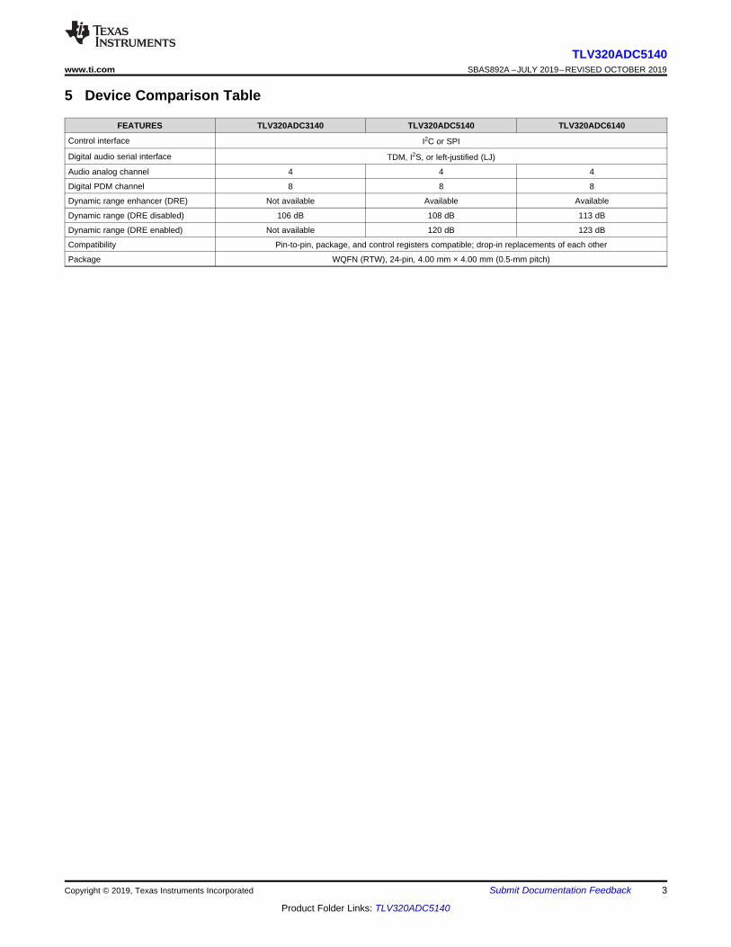
5 Device Comparison Table
FEATURES TLV320ADC3140 TLV320ADC5140 TLV320ADC6140
Control interface I2C or SPI
Digital audio serial interface TDM, I2S, or left-justified (LJ)
Audio analog channel 4 4 4
Digital PDM channel 8 8 8
Dynamic range enhancer (DRE) Not available Available Available
Dynamic range (DRE disabled) 106 dB 108 dB 113 dB
Dynamic range (DRE enabled) Not available 120 dB 123 dB
Compatibility Pin-to-pin, package, and control registers compatible; drop-in replacements of each other
Package WQFN (RTW), 24-pin, 4.00 mm × 4.00 mm (0.5-mm pitch)
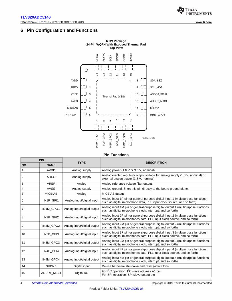
24
DR
EG
7IN
1M
_G
PO
1
1AVDD 18 SDA_SSZ
23
FS
YN
C8
IN2P
_G
PI2
2AREG 17 SCL_MOSI
22
BC
LK
9IN
2M
_G
PO
2
3VREF 16 ADDR0_SCLK
21
SD
OU
T1
0IN
3P
_G
PI3
4AVSS 15 ADDR1_MISO
20
GP
IO1
11
IN3
M_G
PO
3
5MICBIAS 14 SHDNZ
19
IOV
DD
12
IN4P
_G
PI4
6IN1P_GPI1 13 IN4M_GPO4
Not to scale
Thermal Pad (VSS)
4
TLV320ADC5140SBAS892A –JULY 2019–REVISED OCTOBER 2019 www.ti.com
Product Folder Links: TLV320ADC5140
Submit Documentation Feedback Copyright © 2019, Texas Instruments Incorporated
6 Pin Configuration and Functions
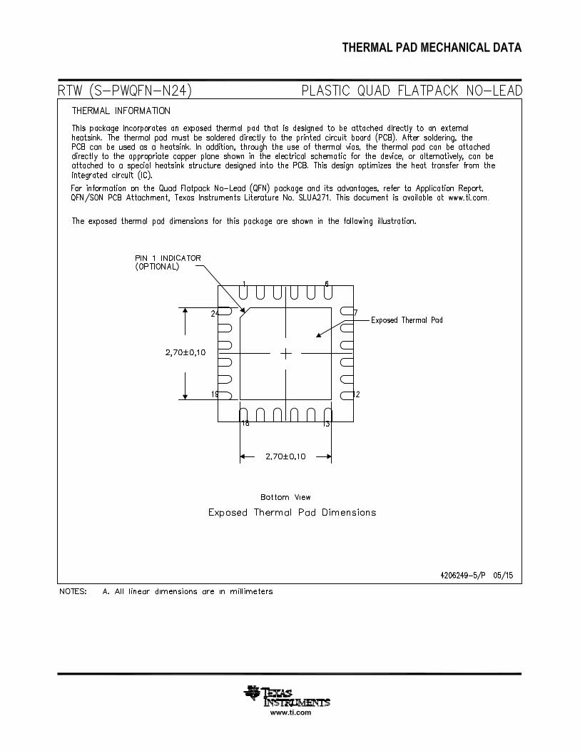
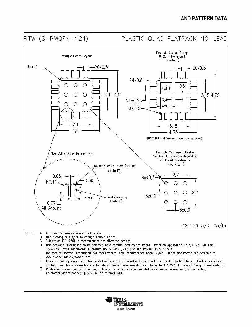
RTW Package24-Pin WQFN With Exposed Thermal Pad
Top View
Pin FunctionsPIN
TYPE DESCRIPTIONNO. NAME1 AVDD Analog supply Analog power (1.8 V or 3.3 V, nominal)
2 AREG Analog supply Analog on-chip regulator output voltage for analog supply (1.8 V, nominal) orexternal analog power (1.8 V, nominal)
3 VREF Analog Analog reference voltage filter output4 AVSS Analog supply Analog ground. Short this pin directly to the board ground plane.5 MICBIAS Analog MICBIAS output
6 IN1P_GPI1 Analog input/digital input Analog input 1P pin or general-purpose digital input 1 (multipurpose functionssuch as digital microphone data, PLL input clock source, and so forth)
7 IN1M_GPO1 Analog input/digital output Analog input 1M pin or general-purpose digital output 1 (multipurpose functionssuch as digital microphone clock, interrupt, and so forth)
8 IN2P_GPI2 Analog input/digital input Analog input 2P pin or general-purpose digital input 2 (multipurpose functionssuch as digital microphones data, PLL input clock source, and so forth)
9 IN2M_GPO2 Analog input/digital output Analog input 2M pin or general-purpose digital output 2 (multipurpose functionssuch as digital microphone clock, interrupt, and so forth)
10 IN3P_GPI3 Analog input/digital input Analog input 3P pin or general-purpose digital input 3 (multipurpose functionssuch as digital microphones data, PLL input clock source, and so forth)
11 IN3M_GPO3 Analog input/digital output Analog input 3M pin or general-purpose digital output 3 (multipurpose functionssuch as digital microphone clock, interrupt, and so forth)
12 IN4P_GPI4 Analog input/digital input Analog input 4P pin or general-purpose digital input 4 (multipurpose functionssuch as digital microphones data, PLL input clock source, and so forth)
13 IN4M_GPO4 Analog input/digital output Analog input 4M pin or general-purpose digital output 4 (multipurpose functionssuch as digital microphone clock, interrupt, and so forth)
14 SHDNZ Digital input Device hardware shutdown and reset (active low)
15 ADDR1_MISO Digital I/O For I2C operation: I2C slave address A1 pinFor SPI operation: SPI slave output pin
5
TLV320ADC5140www.ti.com SBAS892A –JULY 2019–REVISED OCTOBER 2019
Product Folder Links: TLV320ADC5140
Submit Documentation FeedbackCopyright © 2019, Texas Instruments Incorporated
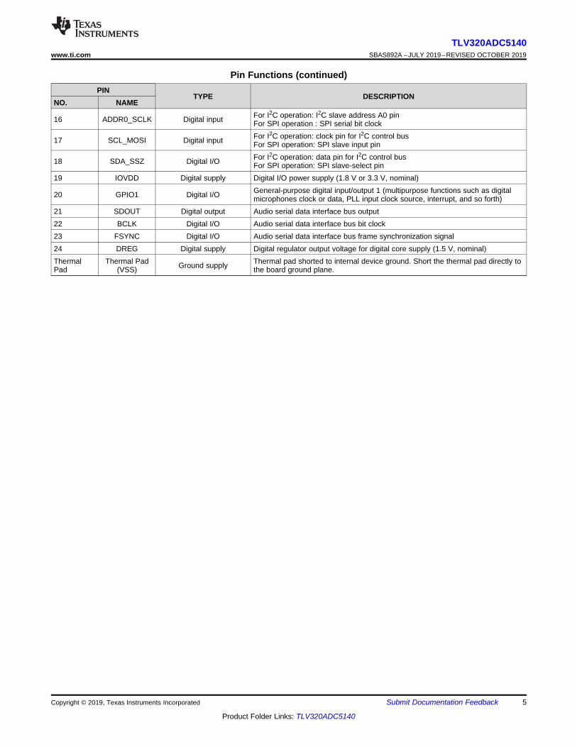
Pin Functions (continued)PIN
TYPE DESCRIPTIONNO. NAME
16 ADDR0_SCLK Digital input For I2C operation: I2C slave address A0 pinFor SPI operation : SPI serial bit clock
17 SCL_MOSI Digital input For I2C operation: clock pin for I2C control busFor SPI operation: SPI slave input pin
18 SDA_SSZ Digital I/O For I2C operation: data pin for I2C control busFor SPI operation: SPI slave-select pin
19 IOVDD Digital supply Digital I/O power supply (1.8 V or 3.3 V, nominal)
20 GPIO1 Digital I/O General-purpose digital input/output 1 (multipurpose functions such as digitalmicrophones clock or data, PLL input clock source, interrupt, and so forth)
21 SDOUT Digital output Audio serial data interface bus output22 BCLK Digital I/O Audio serial data interface bus bit clock23 FSYNC Digital I/O Audio serial data interface bus frame synchronization signal24 DREG Digital supply Digital regulator output voltage for digital core supply (1.5 V, nominal)ThermalPad
Thermal Pad(VSS) Ground supply Thermal pad shorted to internal device ground. Short the thermal pad directly to
the board ground plane.
6
TLV320ADC5140SBAS892A –JULY 2019–REVISED OCTOBER 2019 www.ti.com
Product Folder Links: TLV320ADC5140
Submit Documentation Feedback Copyright © 2019, Texas Instruments Incorporated
(1) Stresses beyond those listed under Absolute Maximum Ratings may cause permanent damage to the device. These are stress ratingsonly, which do not imply functional operation of the device at these or any other conditions beyond those indicated under RecommendedOperating Conditions. Exposure to absolute-maximum-rated conditions for extended periods may affect device reliability.
7 Specifications
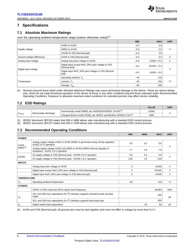
7.1 Absolute Maximum Ratingsover the operating ambient temperature range (unless otherwise noted) (1)
MIN MAX UNIT
Supply voltage
AVDD to AVSS –0.3 3.9
VAREG to AVSS –0.3 2.0
IOVDD to VSS (thermal pad) –0.3 3.9
Ground voltage differences AVSS to VSS (thermal pad) –0.3 0.3 V
Analog input voltage Analog input pins voltage to AVSS –0.3 AVDD + 0.3 V
Digital input voltage
Digital input except INxP_GPIx pins voltage to VSS(thermal pad) –0.3 IOVDD + 0.3
VDigital input INxP_GPIx pins voltage to VSS (thermalpad) –0.3 AVDD + 0.3
Temperature
Operating ambient, TA –40 125
°CJunction, TJ –40 150
Storage, Tstg –65 150
(1) JEDEC document JEP155 states that 500-V HBM allows safe manufacturing with a standard ESD control process.(2) JEDEC document JEP157 states that 250-V CDM allows safe manufacturing with a standard ESD control process.
7.2 ESD RatingsVALUE UNIT
V(ESD) Electrostatic dischargeHuman-body model (HBM), per ANSI/ESDA/JEDEC JS-001 (1) ±2000
VCharged-device model (CDM), per JEDEC specification JESD22-C101 (2) ±500
(1) AVSS and VSS (thermal pad): all ground pins must be tied together and must not differ in voltage by more than 0.2 V.
7.3 Recommended Operating ConditionsMIN NOM MAX UNIT
POWER
AVDD,AREG (1)
Analog supply voltage AVDD to AVSS (AREG is generated using onchip regulator) -AVDD 3.3-V operation 3.0 3.3 3.6
VAnalog supply voltage AVDD and AREG to AVSS (AREG internal regulator isshutdown) - AVDD 1.8-V operation 1.7 1.8 1.9
IOVDDIO supply voltage to VSS (thermal pad) - IOVDD 3.3-V operation 3.0 3.3 3.6
VIO supply voltage to VSS (thermal pad) - IOVDD 1.8-V operation 1.65 1.8 1.95
INPUTS
Analog input pins voltage to AVSS 0 AVDD V
Digital input except INxP_GPIx pins voltage to VSS (thermal pad) 0 IOVDD V
Digital input INxP_GPIx pins voltage to VSS (thermal pad) 0 AVDD V
TEMPERATURE
TA Operating ambient temperature –40 125 °C
OTHERS
GPIOx or GPIx (used as MCLK input) clock frequency 36.864 MHz
Cb
SCL and SDA bus capacitance for I2C interface supports standard-mode and fast-mode 400
pFSCL and SDA bus capacitance for I2C interface supports fast-mode plus 550
CL Digital output load capacitance 20 50 pF

7
TLV320ADC5140www.ti.com SBAS892A –JULY 2019–REVISED OCTOBER 2019
Product Folder Links: TLV320ADC5140
Submit Documentation FeedbackCopyright © 2019, Texas Instruments Incorporated
(1) For more information about traditional and new thermal metrics, see the Semiconductor and IC Package Thermal Metrics applicationreport.
7.4 Thermal Information
THERMAL METRIC (1)
TLV320ADCx140
UNITRTW (WQFN)
24 PINS
RθJA Junction-to-ambient thermal resistance 32.6 °C/W
RθJC(top) Junction-to-case (top) thermal resistance 25.0 °C/W
RθJB Junction-to-board thermal resistance 11.9 °C/W
ψJT Junction-to-top characterization parameter 0.2 °C/W
ψJB Junction-to-board characterization parameter 11.9 °C/W
RθJC(bot) Junction-to-case (bottom) thermal resistance 2.9 °C/W
(1) Ratio of output level with 1-kHz full-scale sine-wave input, to the output level with the AC signal input shorted to ground, measured A-weighted over a 20-Hz to 20-kHz bandwidth using an audio analyzer.
(2) All performance measurements done with 20-kHz low-pass filter and, where noted, A-weighted filter. Failure to use such a filter mayresult in higher THD and lower SNR and dynamic range readings than shown in the Electrical Characteristics. The low-pass filterremoves out-of-band noise, which, although not audible, may affect dynamic specification values.
7.5 Electrical Characteristicsat TA = 25°C, AVDD = 3.3 V, IOVDD = 3.3 V, fIN = 1-kHz sinusoidal signal, fS = 48 kHz, 32-bit audio data, BCLK = 256 × fS,TDM slave mode, PLL on (unless otherwise noted)
PARAMETER TEST CONDITIONS MIN TYP MAX UNIT
ADC CONFIGURATION
AC input impedance
Input pins INxP or INxM, 2.5-kΩ input impedanceselection 2.5
kΩInput pins INxP or INxM, 10-kΩ input impedanceselection 10
Input pins INxP or INxM, 20-kΩ input impednaceselection 20
Channel gain range Programmable range with 1-dB steps 0 42 dB
ADC PERFORMANCE FOR LINE/MICROPHONE INPUT RECORDING : AVDD 3.3-V OPERATION
Differential input full-scaleAC signal voltage AC-coupled input 2 VRMS
Single-ended input full-scale AC signal voltage AC-coupled input 1 VRMS
SNR Signal-to-noise ratio, A-weighted (1) (2)
IN1 differential input selected and AC signal shorted toground, DRE enabled (DRE_LVL = –36 dB,DRE_MAXGAIN = 24 dB), 2.5-kΩ input impedanceselection
112 119
dB
IN1 differential input selected and AC signal shorted toground, DRE enabled (DRE_LVL = –36 dB,DRE_MAXGAIN = 24 dB), 10-kΩ input impedanceselection
116
IN1 differential input selected and AC signal shorted toground, DRE disabled, 10-kΩ input impedanceselection, 0-dB channel gain
102 107
IN1 differential input selected and AC signal shorted toground, DRE disabled, 10-kΩ input impedanceselection, 12-dB channel gain
102
DR Dynamic range, A-weighted (2)
IN1 differential input selected and –60-dB full-scale ACsignal input, DRE enabled (DRE_LVL = –36 dB,DRE_MAXGAIN = 24 dB), 2.5-kΩ input impedanceselection
120
dB
IN1 differential input selected and –60-dB full-scale ACsignal input, DRE enabled (DRE_LVL = –36 dB,DRE_MAXGAIN = 24 dB), 10-kΩ input impedanceselection
117
IN1 differential input selected and –60-dB full-scale ACsignal input, DRE disabled, 10-kΩ input impedanceselection, 0-dB channel gain
108
IN1 differential input selected and –72-dB full-scale ACsignal input, DRE disabled, 10-kΩ input impedanceselection, 12-dB channel gain
103
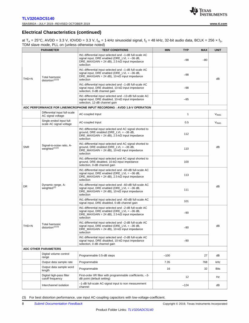
8
TLV320ADC5140SBAS892A –JULY 2019–REVISED OCTOBER 2019 www.ti.com
Product Folder Links: TLV320ADC5140
Submit Documentation Feedback Copyright © 2019, Texas Instruments Incorporated
Electrical Characteristics (continued)at TA = 25°C, AVDD = 3.3 V, IOVDD = 3.3 V, fIN = 1-kHz sinusoidal signal, fS = 48 kHz, 32-bit audio data, BCLK = 256 × fS,TDM slave mode, PLL on (unless otherwise noted)
PARAMETER TEST CONDITIONS MIN TYP MAX UNIT
(3) For best distortion performance, use input AC-coupling capacitors with low-voltage-coefficient.
THD+N Total harmonicdistortion (2) (3)
IN1 differential input selected and –1-dB full-scale ACsignal input, DRE enabled (DRE_LVL = –36 dB,DRE_MAXGAIN = 24 dB), 2.5-kΩ input impedanceselection
–98 –80
dB
IN1 differential input selected and –1-dB full-scale ACsignal input, DRE enabled (DRE_LVL = –36 dB,DRE_MAXGAIN = 24 dB), 10-kΩ input impedanceselection
–98
IN1 differential input selected and –1-dB full-scale ACsignal input, DRE disabled, 10-kΩ input impedanceselection, 0-dB channel gain
–98
IN1 differential input selected and –13-dB full-scale ACsignal input, DRE disabled, 10-kΩ input impedanceselection, 12-dB channel gain
–95
ADC PERFORMANCE FOR LINE/MICROPHONE INPUT RECORDING : AVDD 1.8-V OPERATION
Differential input full-scaleAC signal voltage AC-coupled Input 1 VRMS
Single-ended input full-scale AC signal voltage AC-coupled Input 0.5 VRMS
SNR Signal-to-noise ratio, A-weighted (1) (2)
IN1 differential input selected and AC signal shorted toground, DRE enabled (DRE_LVL = –36 dB,DRE_MAXGAIN = 24 dB), 2.5-kΩ input impedanceselection
112
dBIN1 differential input selected and AC signal shorted toground, DRE enabled (DRE_LVL = –36 dB,DRE_MAXGAIN = 24 dB), 10-kΩ input impedanceselection
110
IN1 differential input selected and AC signal shorted toground, DRE disabled, 10-kΩ input impedanceselection, 0-dB channel gain
100
DR Dynamic range, A-weighted (2)
IN1 differential input selected and –60-dB full-scale ACsignal input, DRE enabled (DRE_LVL = –36 dB,DRE_MAXGAIN = 24 dB), 2.5-kΩ input impedanceselection
113
dBIN1 differential input selected and –60-dB full-scale ACsignal input, DRE enabled (DRE_LVL = –36 dB,DRE_MAXGAIN = 24 dB), 10-kΩ input impedanceselection
111
IN1 differential input selected and –60-dB full-scale ACsignal input, DRE disabled, 0-dB channel gain 101
THD+N Total harmonicdistortion (2) (3)
IN1 differential input selected and –2-dB full-scale ACsignal input, DRE enabled (DRE_LVL = –36 dB,DRE_MAXGAIN = 24 dB), 2.5-kΩ input impedanceselection
–90
dBIN1 differential input selected and –2-dB full-scale ACsignal input, DRE enabled (DRE_LVL = –36 dB,DRE_MAXGAIN = 24 dB), 10-kΩ input impedanceselection
–90
IN1 differential input selected and –2-dB full-scale ACsignal Input, DRE disabled, 10-kΩ input impedanceselection, 0 dB channel gain
–90
ADC OTHER PARAMETERS
Digital volume controlrange Programmable 0.5-dB steps –100 27 dB
Output data sample rate Programmable 7.35 768 kHz
Output data sample wordlength Programmable 16 32 Bits
Digital high-pass filtercutoff frequency
First-order IIR filter with programmable coefficients, –3-dB point (default setting) 12 Hz
Interchannel isolation –1-dB full-scale AC-signal input to non measurementchannel –124 dB
9
TLV320ADC5140www.ti.com SBAS892A –JULY 2019–REVISED OCTOBER 2019
Product Folder Links: TLV320ADC5140
Submit Documentation FeedbackCopyright © 2019, Texas Instruments Incorporated
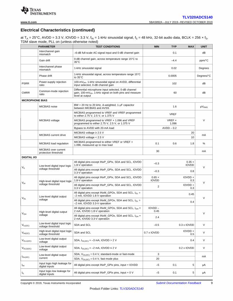
Electrical Characteristics (continued)at TA = 25°C, AVDD = 3.3 V, IOVDD = 3.3 V, fIN = 1-kHz sinusoidal signal, fS = 48 kHz, 32-bit audio data, BCLK = 256 × fS,TDM slave mode, PLL on (unless otherwise noted)
PARAMETER TEST CONDITIONS MIN TYP MAX UNIT
Interchannel gainmismatch –6-dB full-scale AC-signal input and 0-dB channel gain 0.1 dB
Gain drift 0-dB channel gain, across temperature range 15°C to35°C –4.4 ppm/°C
Interchannel phasemismatch 1-kHz sinusoidal signal 0.02 Degrees
Phase drift 1-kHz sinusoidal signal, across temperature range 15°Cto 35°C 0.0005 Degrees/°C
PSRR Power-supply rejectionratio
100-mVPP, 1-kHz sinusoidal signal on AVDD, differentialinput selected, 0-dB channel gain 102 dB
CMRR Common-mode rejectionratio
Differential microphone input selected, 0-dB channelgain, 100-mVPP, 1-kHz signal on both pins and measurelevel at output
60 dB
MICROPHONE BIAS
MICBIAS noise BW = 20 Hz to 20 kHz, A-weighted, 1-μF capacitorbetween MICBIAS and AVSS 1.6 µVRMS
MICBIAS voltage
MICBIAS programmed to VREF and VREF programmedto either 2.75 V, 2.5 V, or 1.375 V VREF
VMICBIAS programmed to VREF × 1.096 and VREFprogrammed to either 2.75 V, 2.5 V, or 1.375 V
VREF ×1.096
Bypass to AVDD with 20-mA load AVDD – 0.2
MICBIAS current driveMICBIAS voltage ≥ 2.5 V 20
mAMICBIAS voltage < 2.5 V 10
MICBIAS load regulation MICBIAS programmed to either VREF or VREF ×1.096, measured up to max load 0.1 0.6 1.8 %
MICBIAS over currentprotection threshold 30 mA
DIGITAL I/O
VILLow-level digital input logicvoltage threshold
All digital pins except INxP_GPIx, SDA and SCL, IOVDD1.8-V operation –0.3 0.35 ×
IOVDDV
All digital pins except INxP_GPIx, SDA and SCL, IOVDD3.3-V operation –0.3 0.8
VIHHigh-level digital input logicvoltage threshold
All digital pins except INxP_GPIx, SDA and SCL, IOVDD1.8-V operation
0.65 ×IOVDD
IOVDD +0.3
VAll digital pins except INxP_GPIx, SDA and SCL, IOVDD3.3-V operation 2 IOVDD +
0.3
VOLLow-level digital outputvoltage
All digital pins except INxM_GPOx, SDA and SCL, IOL =–2 mA, IOVDD 1.8-V operation 0.45
VAll digital pins except INxM_GPOx, SDA and SCL, IOL =–2 mA, IOVDD 3.3-V operation 0.4
VOHHigh-level digital outputvoltage
All digital pins except INxM_GPOx, SDA and SCL, IOH =2 mA, IOVDD 1.8-V operation
IOVDD –0.45
VAll digital pins except INxM_GPOx, SDA and SCL, IOH =2 mA, IOVDD 3.3-V operation 2.4
VIL(I2C)Low-level digital input logicvoltage threshold SDA and SCL –0.5 0.3 x IOVDD V
VIH(I2C)High-level digital input logicvoltage threshold SDA and SCL 0.7 x IOVDD IOVDD +
0.5 V
VOL1(I2C)Low-level digital outputvoltage SDA, IOL(I2C) = –3 mA, IOVDD > 2 V 0.4 V
VOL2(I2C)Low-level digital outputvoltage SDA, IOL(I2C) = –2 mA, IOVDD ≤ 2 V 0.2 x IOVDD V
IOL(I2C)Low-level digital outputcurrent
SDA, VOL(I2C) = 0.4 V, standard-mode or fast-mode 3mA
SDA, VOL(I2C) = 0.4 V, fast-mode plus 20
IIHInput logic-high leakage fordigital inputs All digital pins except INxP_GPIx pins, input = IOVDD –5 0.1 5 µA
IILInput logic-low leakage fordigital inputs All digital pins except INxP_GPIx pins, input = 0 V –5 0.1 5 µA
10
TLV320ADC5140SBAS892A –JULY 2019–REVISED OCTOBER 2019 www.ti.com
Product Folder Links: TLV320ADC5140
Submit Documentation Feedback Copyright © 2019, Texas Instruments Incorporated
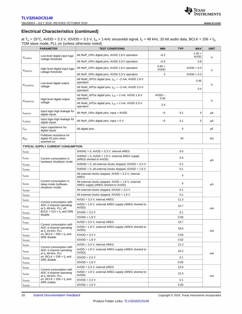
Electrical Characteristics (continued)at TA = 25°C, AVDD = 3.3 V, IOVDD = 3.3 V, fIN = 1-kHz sinusoidal signal, fS = 48 kHz, 32-bit audio data, BCLK = 256 × fS,TDM slave mode, PLL on (unless otherwise noted)
PARAMETER TEST CONDITIONS MIN TYP MAX UNIT
VIL(GPIx)Low-level digital input logicvoltage threshold
All INxP_GPIx digital pins, AVDD 1.8-V operation –0.3 0.35 ×AVDD V
All INxP_GPIx digital pins, AVDD 3.3-V operation –0.3 0.8
VIH(GPIx)High-level digital input logicvoltage threshold
All INxP_GPIx digital pins, AVDD 1.8-V operation 0.65 ×AVDD AVDD + 0.3
VAll INxP_GPIx digital pins, AVDD 3.3-V operation 2 AVDD + 0.3
VOL(GPOx)Low-level digital outputvoltage
All INxM_GPOx digital pins, IOL = –2 mA, AVDD 1.8-Voperation 0.45
VAll INxM_GPOx digital pins, IOL = –2 mA, AVDD 3.3-Voperation 0.4
VOH(GPOx)High-level digital outputvoltage
All INxM_GPOx digital pins, IOH = 2 mA, AVDD 1.8-Voperation
AVDD –0.45
VAll INxM_GPOx digital pins, IOH = 2 mA, AVDD 3.3-Voperation 2.4
IIH(GPIx)Input logic-high leakage fordigital inputs All INxP_GPIx digital pins, input = AVDD –5 0.1 5 µA
IIL(GPIx)Input logic-high leakage fordigital inputs All INxP_GPIx digital pins, input = 0 V –5 0.1 5 µA
CINInput capacitance fordigital inputs All digital pins 5 pF
RPD
Pulldown resistance fordigital I/O pins whenasserted on
20 kΩ
TYPICAL SUPPLY CURRENT CONSUMPTION
IAVDD
Current consumption inhardware shutdown mode
SHDNZ = 0, AVDD = 3.3 V, internal AREG 0.5
µAIAVDD
SHDNZ = 0, AVDD = 1.8 V, external AREG supply(AREG shorted to AVDD) 0.5
IIOVDD SHDNZ = 0, all external clocks stopped, IOVDD = 3.3 V 0.1
IIOVDD SHDNZ = 0, all external clocks stopped, IOVDD = 1.8 V 0.1
IAVDD
Current consumption insleep mode (softwareshutdown mode)
All external clocks stopped, AVDD = 3.3 V, internalAREG 5
µAIAVDDAll external clocks stopped, AVDD = 1.8 V, externalAREG supply (AREG shorted to AVDD) 5
IIOVDD All external clocks stopped, IOVDD = 3.3 V 0.1
IIOVDD All external clocks stopped, IOVDD = 1.8 V 0.1
IAVDDCurrent consumption withADC 2-channel operatingat fS 48-kHz, PLL off,BCLK = 512 × fS and DREdisable
AVDD = 3.3 V, internal AREG 11.3
mAIAVDD
AVDD = 1.8 V, external AREG supply (AREG shorted toAVDD) 10.7
IIOVDD IOVDD = 3.3 V 0.1
IIOVDD IOVDD = 1.8 V 0.05
IAVDDCurrent consumption withADC 4-channel operatingat fS 16-kHz, PLLon, BCLK = 256 × fS andDRE disable
AVDD = 3.3 V, internal AREG 19.7
mAIAVDD
AVDD = 1.8 V, external AREG supply (AREG shorted toAVDD) 18.6
IIOVDD IOVDD = 3.3 V 0.05
IIOVDD IOVDD = 1.8 V 0.02
IAVDDCurrent consumption withADC 4-channel operatingat fS 48-kHz, PLLon, BCLK = 256 × fS andDRE disable
AVDD = 3.3 V, internal AREG 21.3
mAIAVDD
AVDD = 1.8 V, external AREG supply (AREG shorted toAVDD) 20.2
IIOVDD IOVDD = 3.3 V 0.1
IIOVDD IOVDD = 1.8 V 0.05
IAVDDCurrent consumption withADC 4-channel operatingat fS 48-kHz, PLLon, BCLK = 256 × fS andDRE enable
AVDD = 3.3 V, internal AREG 23.6
mAIAVDD
AVDD = 1.8 V, external AREG supply (AREG shorted toAVDD) 22.3
IIOVDD IOVDD = 3.3 V 0.1
IIOVDD IOVDD = 1.8 V 0.05
11
TLV320ADC5140www.ti.com SBAS892A –JULY 2019–REVISED OCTOBER 2019
Product Folder Links: TLV320ADC5140
Submit Documentation FeedbackCopyright © 2019, Texas Instruments Incorporated
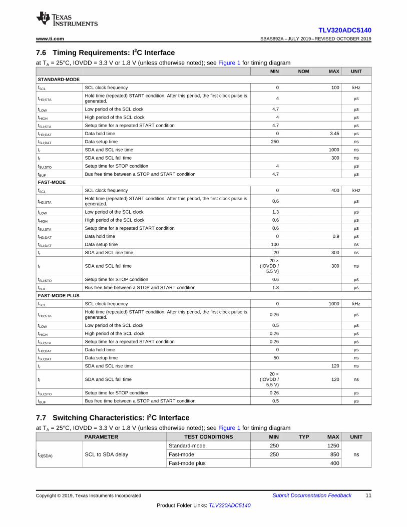
7.6 Timing Requirements: I2C Interfaceat TA = 25°C, IOVDD = 3.3 V or 1.8 V (unless otherwise noted); see Figure 1 for timing diagram
MIN NOM MAX UNIT
STANDARD-MODE
fSCL SCL clock frequency 0 100 kHz
tHD;STAHold time (repeated) START condition. After this period, the first clock pulse isgenerated. 4 μs
tLOW Low period of the SCL clock 4.7 μs
tHIGH High period of the SCL clock 4 μs
tSU;STA Setup time for a repeated START condition 4.7 μs
tHD;DAT Data hold time 0 3.45 μs
tSU;DAT Data setup time 250 ns
tr SDA and SCL rise time 1000 ns
tf SDA and SCL fall time 300 ns
tSU;STO Setup time for STOP condition 4 μs
tBUF Bus free time between a STOP and START condition 4.7 μs
FAST-MODE
fSCL SCL clock frequency 0 400 kHz
tHD;STAHold time (repeated) START condition. After this period, the first clock pulse isgenerated. 0.6 μs
tLOW Low period of the SCL clock 1.3 μs
tHIGH High period of the SCL clock 0.6 μs
tSU;STA Setup time for a repeated START condition 0.6 μs
tHD;DAT Data hold time 0 0.9 μs
tSU;DAT Data setup time 100 ns
tr SDA and SCL rise time 20 300 ns
tf SDA and SCL fall time20 ×
(IOVDD /5.5 V)
300 ns
tSU;STO Setup time for STOP condition 0.6 μs
tBUF Bus free time between a STOP and START condition 1.3 μs
FAST-MODE PLUS
fSCL SCL clock frequency 0 1000 kHz
tHD;STAHold time (repeated) START condition. After this period, the first clock pulse isgenerated. 0.26 μs
tLOW Low period of the SCL clock 0.5 μs
tHIGH High period of the SCL clock 0.26 μs
tSU;STA Setup time for a repeated START condition 0.26 μs
tHD;DAT Data hold time 0 μs
tSU;DAT Data setup time 50 ns
tr SDA and SCL rise time 120 ns
tf SDA and SCL fall time20 ×
(IOVDD /5.5 V)
120 ns
tSU;STO Setup time for STOP condition 0.26 μs
tBUF Bus free time between a STOP and START condition 0.5 μs
7.7 Switching Characteristics: I2C Interfaceat TA = 25°C, IOVDD = 3.3 V or 1.8 V (unless otherwise noted); see Figure 1 for timing diagram
PARAMETER TEST CONDITIONS MIN TYP MAX UNIT
td(SDA) SCL to SDA delayStandard-mode 250 1250
nsFast-mode 250 850Fast-mode plus 400
12
TLV320ADC5140SBAS892A –JULY 2019–REVISED OCTOBER 2019 www.ti.com
Product Folder Links: TLV320ADC5140
Submit Documentation Feedback Copyright © 2019, Texas Instruments Incorporated
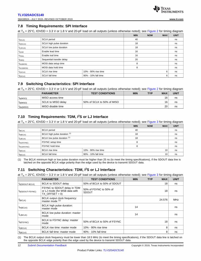
7.8 Timing Requirements: SPI Interfaceat TA = 25°C, IOVDD = 3.3 V or 1.8 V and 20-pF load on all outputs (unless otherwise noted); see Figure 2 for timing diagram
MIN NOM MAX UNIT
t(SCLK) SCLK period 40 ns
tH(SCLK) SCLK high pulse duration 18 ns
tL(SCLK) SCLK low pulse duration 18 ns
tLEAD Enable lead time 16 ns
tTRAIL Enable trail time 16 ns
tDSEQ Sequential transfer delay 20 ns
tSU(MOSI) MOSI data setup time 8 ns
tHLD(MOSI) MOSI data hold time 8 ns
tr(SCLK) SCLK rise time 10% - 90% rise time 6 ns
tf(SCLK) SCLK fall time 90% - 10% fall time 6 ns
7.9 Switching Characteristics: SPI Interfaceat TA = 25°C, IOVDD = 3.3 V or 1.8 V and 20-pF load on all outputs (unless otherwise noted); see Figure 2 for timing diagram
PARAMETER TEST CONDITIONS MIN TYP MAX UNITta(MISO) MISO access time 16 nstd(MISO) SCLK to MISO delay 50% of SCLK to 50% of MISO 16 nstdis(MISO) MISO disable time 20 ns
(1) The BCLK minimum high or low pulse duration must be higher than 25 ns (to meet the timing specifications), if the SDOUT data line islatched on the opposite BCLK edge polarity than the edge used by the device to transmit SDOUT data.
7.10 Timing Requirements: TDM, I2S or LJ Interfaceat TA = 25°C, IOVDD = 3.3 V or 1.8 V and 20-pF load on all outputs (unless otherwise noted); see Figure 3 for timing diagram
MIN NOM MAX UNIT
t(BCLK) BCLK period 40 ns
tH(BCLK) BCLK high pulse duration (1) 18 ns
tL(BCLK) BCLK low pulse duration (1) 18 ns
tSU(FSYNC) FSYNC setup time 8 ns
tHLD(FSYNC) FSYNC hold time 8 ns
tr(BCLK) BCLK rise time 10% - 90% rise time 10 ns
tf(BCLK) BCLK fall time 90% - 10% fall time 10 ns
(1) The BCLK output clock frequency must be lower than 18.5 MHz (to meet the timing specifications), if the SDOUT data line is latched onthe opposite BCLK edge polarity than the edge used by the device to transmit SDOUT data.
7.11 Switching Characteristics: TDM, I2S or LJ Interfaceat TA = 25°C, IOVDD = 3.3 V or 1.8 V and 20-pF load on all outputs (unless otherwise noted); see Figure 3 for timing diagram
PARAMETER TEST CONDITIONS MIN TYP MAX UNITtd(SDOUT-BCLK) BCLK to SDOUT delay 50% of BCLK to 50% of SDOUT 18 ns
td(SDOUT-FSYNC)
FSYNC to SDOUT delay in TDMor LJ mode (for MSB data withTX_OFFSET = 0)
50% of FSYNC to 50% ofSDOUT 18 ns
f(BCLK)BCLK output clock frequency:master mode (1) 24.576 MHz
tH(BCLK)BCLK high pulse duration:master mode 14 ns
tL(BCLK)BCLK low pulse duration: mastermode 14 ns
td(FSYNC)BCLK to FSYNC delay: mastermode 50% of BCLK to 50% of FSYNC 18 ns
tr(BCLK) BCLK rise time: master mode 10% - 90% rise time 8 nstf(BCLK) BCLK fall time: master mode 90% - 10% fall time 8 ns
SCLK
SSZ
MISO
MOSI
tLEAD
tDSEQ
t(SCLK)
tH(SCLK)
tL(SCLK)
tf(SCLK) tr(SCLK)
tLAG
tdis(MISO)
tSU(MOSI)
ta(MISO)
td(MISO)
tHLD(MOSI)
MSB IN
MSB OUT BIT6...1 LSB OUT
LSB INBIT6...1
STO STA
SDA
SCL
STA STO
tBUF
tHD;STA
tHD;DAT tSU;DAT tSU;STA tSU;STO
tHD;STAtLOW
tHIGH
tr
tf
td(SDA)
13
TLV320ADC5140www.ti.com SBAS892A –JULY 2019–REVISED OCTOBER 2019
Product Folder Links: TLV320ADC5140
Submit Documentation FeedbackCopyright © 2019, Texas Instruments Incorporated
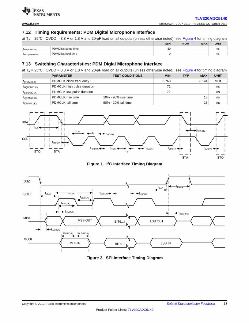
7.12 Timing Requirements: PDM Digital Microphone Interfaceat TA = 25°C, IOVDD = 3.3 V or 1.8 V and 20-pF load on all outputs (unless otherwise noted); see Figure 4 for timing diagram
MIN NOM MAX UNIT
tSU(PDMDINx) PDMDINx setup time 30 ns
tHLD(PDMDINx) PDMDINx hold time 0 ns
7.13 Switching Characteristics: PDM Digial Microphone Interfaceat TA = 25°C, IOVDD = 3.3 V or 1.8 V and 20-pF load on all outputs (unless otherwise noted); see Figure 4 for timing diagram
PARAMETER TEST CONDITIONS MIN TYP MAX UNITf(PDMCLK) PDMCLK clock frequency 0.768 6.144 MHztH(PDMCLK) PDMCLK high pulse duration 72 nstL(PDMCLK) PDMCLK low pulse duration 72 nstr(PDMCLK) PDMCLK rise time 10% - 90% rise time 18 nstf(PDMCLK) PDMCLK fall time 90% - 10% fall time 18 ns
Figure 1. I2C Interface Timing Diagram
Figure 2. SPI Interface Timing Diagram
PDMCLK
PDMDINx
tSU(PDMDINx) tHLD(PDMDINx) tSU(PDMDINx) tHLD(PDMDINx)
tr(PDMCLK)
tf(PDMCLK)
Falling Edge Captured Rising Edge Captured
tH(PDMCLK) tL(PDMCLK)
t(PDMCLK)
FSYNC
BCLK
tH(BCLK)
tL(BCLK)
tr(BCLK) tf(BCLK)
tSU(FSYNC)tHLD(FSYNC)
td(SDOUT-FSYNC)td(SDOUT-BCLK)
SDOUT
t(BCLK)
td(FSYNC)
14
TLV320ADC5140SBAS892A –JULY 2019–REVISED OCTOBER 2019 www.ti.com
Product Folder Links: TLV320ADC5140
Submit Documentation Feedback Copyright © 2019, Texas Instruments Incorporated
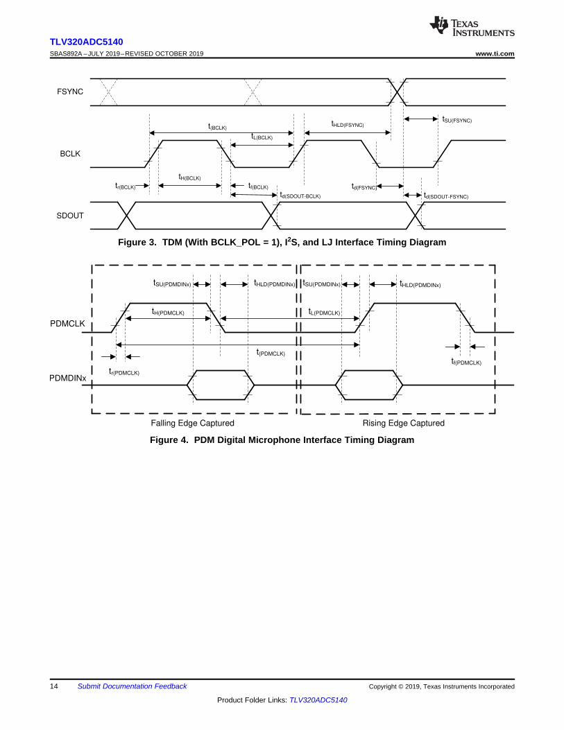
Figure 3. TDM (With BCLK_POL = 1), I2S, and LJ Interface Timing Diagram
Figure 4. PDM Digital Microphone Interface Timing Diagram
Input Amplitude (dB)
TH
D+
N (
dB
FS
)
-130 -115 -100 -85 -70 -55 -40 -25 -10 0
-130
-120
-110
-100
-90
-80
-70
-60
THD+D101
Channel-1 : DRE enabled
Channel-2 : DRE enabled
Channel-3 : DRE enabled
Channel-4 : DRE enabled
Input Amplitude (dB)
TH
D+
N (
dB
FS
)
-130 -115 -100 -85 -70 -55 -40 -25 -10 0
-130
-120
-110
-100
-90
-80
-70
-60
THD+D101
Channel-1 : DRE disabled
Channel-2 : DRE disabled
Channel-3 : DRE disabled
Channel-4 : DRE disabled
Input Amplitude (dB)
TH
D+
N (
dB
FS
)
-130 -115 -100 -85 -70 -55 -40 -25 -10 0
-130
-120
-110
-100
-90
-80
-70
-60
THD+D101
Channel-1 : DRE enabled
Channel-2 : DRE enabled
Channel-3 : DRE enabled
Channel-4 : DRE enabled
Input Amplitude (dB)
TH
D+
N (
dB
FS
)
-130 -115 -100 -85 -70 -55 -40 -25 -10 0
-130
-120
-110
-100
-90
-80
-70
-60
THD+D101
Channel-1 : DRE disabled
Channel-2 : DRE disabled
Channel-3 : DRE disabled
Channel-4 : DRE disabled
15
TLV320ADC5140www.ti.com SBAS892A –JULY 2019–REVISED OCTOBER 2019
Product Folder Links: TLV320ADC5140
Submit Documentation FeedbackCopyright © 2019, Texas Instruments Incorporated
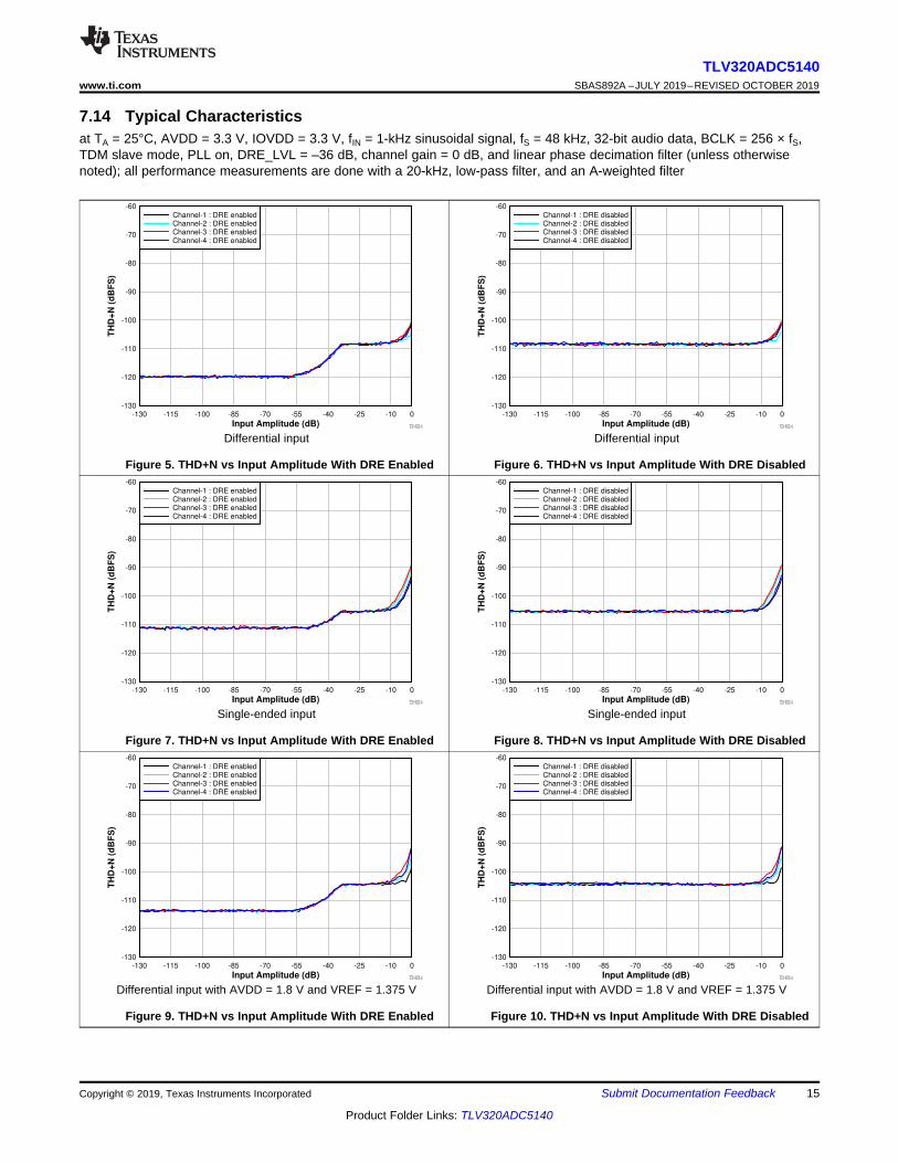
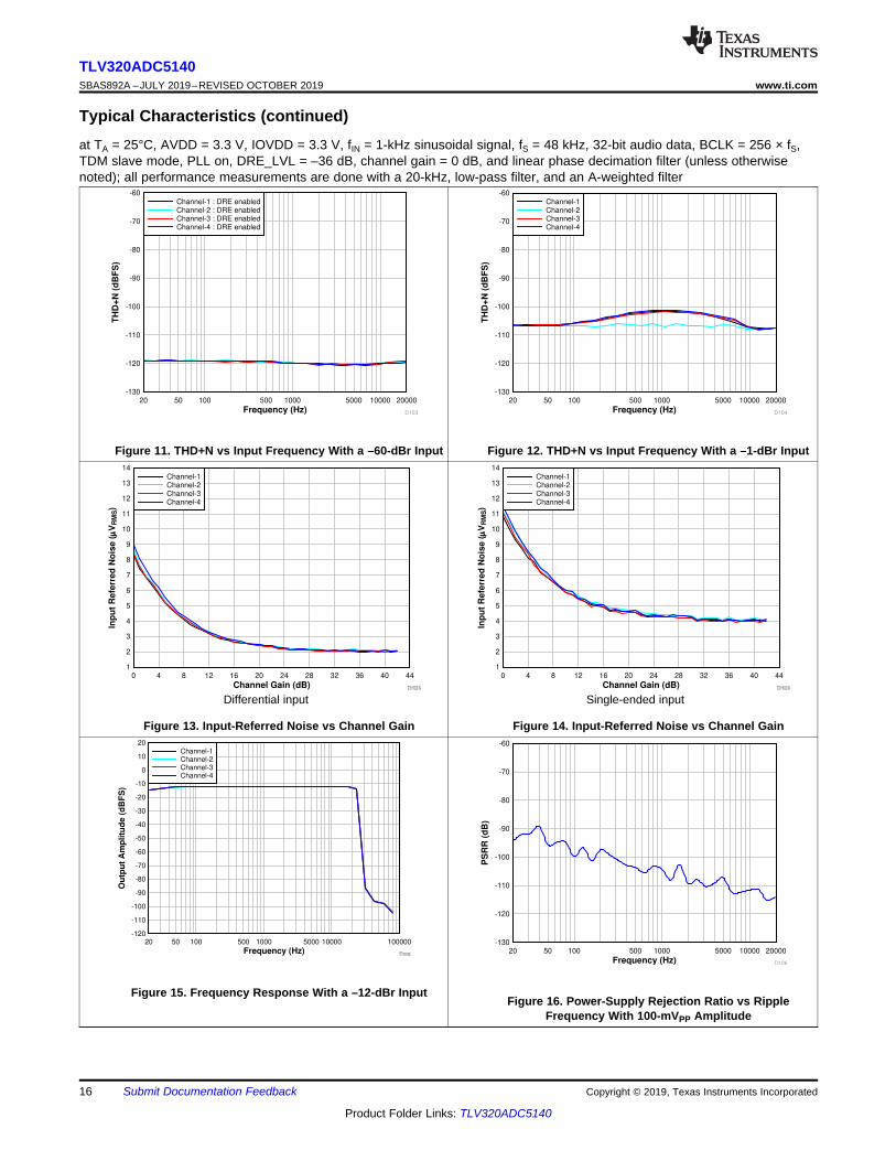
7.14 Typical Characteristicsat TA = 25°C, AVDD = 3.3 V, IOVDD = 3.3 V, fIN = 1-kHz sinusoidal signal, fS = 48 kHz, 32-bit audio data, BCLK = 256 × fS,TDM slave mode, PLL on, DRE_LVL = –36 dB, channel gain = 0 dB, and linear phase decimation filter (unless otherwisenoted); all performance measurements are done with a 20-kHz, low-pass filter, and an A-weighted filter
Differential input
Figure 5. THD+N vs Input Amplitude With DRE Enabled
Differential input
Figure 6. THD+N vs Input Amplitude With DRE Disabled
Single-ended input
Figure 7. THD+N vs Input Amplitude With DRE Enabled
Single-ended input
Figure 8. THD+N vs Input Amplitude With DRE Disabled
Differential input with AVDD = 1.8 V and VREF = 1.375 V
Figure 9. THD+N vs Input Amplitude With DRE Enabled
Differential input with AVDD = 1.8 V and VREF = 1.375 V
Figure 10. THD+N vs Input Amplitude With DRE Disabled
Frequency (Hz)
PS
RR
(d
B)
20 50 100 500 1000 5000 10000 20000
-130
-120
-110
-100
-90
-80
-70
-60
D106
Frequency (Hz)
Ou
tpu
t A
mp
litu
de (
dB
FS
)
20 50 100 500 1000 5000 10000 100000-120
-110
-100
-90
-80
-70
-60
-50
-40
-30
-20
-10
0
10
20
FreqOutp
Channel-1Channel-2Channel-3Channel-4
Channel Gain (dB)
Inp
ut
Re
ferr
ed
No
ise
(P
VR
MS)
0 4 8 12 16 20 24 28 32 36 40 44
1
2
3
4
5
6
7
8
9
10
11
12
13
14
THD+D105
Channel-1
Channel-2
Channel-3
Channel-4
Channel Gain (dB)
Inp
ut
Re
ferr
ed
No
ise
(P
VR
MS)
0 4 8 12 16 20 24 28 32 36 40 44
1
2
3
4
5
6
7
8
9
10
11
12
13
14
THD+D105
Channel-1
Channel-2
Channel-3
Channel-4
Frequency (Hz)
TH
D+
N (
dB
FS
)
20 50 100 500 1000 5000 10000 20000
-130
-120
-110
-100
-90
-80
-70
-60
D103
Channel-1 : DRE enabled
Channel-2 : DRE enabled
Channel-3 : DRE enabled
Channel-4 : DRE enabled
Frequency (Hz)
TH
D+
N (
dB
FS
)
20 50 100 500 1000 5000 10000 20000
-130
-120
-110
-100
-90
-80
-70
-60
D104
Channel-1
Channel-2
Channel-3
Channel-4
16
TLV320ADC5140SBAS892A –JULY 2019–REVISED OCTOBER 2019 www.ti.com
Product Folder Links: TLV320ADC5140
Submit Documentation Feedback Copyright © 2019, Texas Instruments Incorporated
Typical Characteristics (continued)at TA = 25°C, AVDD = 3.3 V, IOVDD = 3.3 V, fIN = 1-kHz sinusoidal signal, fS = 48 kHz, 32-bit audio data, BCLK = 256 × fS,TDM slave mode, PLL on, DRE_LVL = –36 dB, channel gain = 0 dB, and linear phase decimation filter (unless otherwisenoted); all performance measurements are done with a 20-kHz, low-pass filter, and an A-weighted filter
Figure 11. THD+N vs Input Frequency With a –60-dBr Input Figure 12. THD+N vs Input Frequency With a –1-dBr Input
Differential input
Figure 13. Input-Referred Noise vs Channel Gain
Single-ended input
Figure 14. Input-Referred Noise vs Channel Gain
Figure 15. Frequency Response With a –12-dBr InputFigure 16. Power-Supply Rejection Ratio vs Ripple
Frequency With 100-mVPP Amplitude
Frequency (Hz)
Ou
tpu
t A
mp
litu
de (
dB
FS
)
20 50 100 500 1000 5000 10000 20000
-200
-180
-160
-140
-120
-100
-80
-60
-40
-20
0
FFT_
Channel-1 : DRE enabled
Channel-2 : DRE enabled
Channel-3 : DRE enabled
Channel-4 : DRE enabled
Frequency (Hz)
Ou
tpu
t A
mp
litu
de (
dB
FS
)
20 50 100 500 1000 5000 10000 20000
-200
-180
-160
-140
-120
-100
-80
-60
-40
-20
0
FFT_
Channel-1 : DRE disabled
Channel-2 : DRE disabled
Channel-3 : DRE disabled
Channel-4 : DRE disabled
Frequency (Hz)
Ou
tpu
t A
mp
litu
de (
dB
FS
)
20 50 100 500 1000 5000 10000 20000
-200
-180
-160
-140
-120
-100
-80
-60
-40
-20
0
FFT_
Channel-1 : DRE enabled
Channel-2 : DRE enabled
Channel-3 : DRE enabled
Channel-4 : DRE enabled
Frequency (Hz)
Ou
tpu
t A
mp
litu
de (
dB
FS
)
20 50 100 500 1000 5000 10000 20000
-200
-180
-160
-140
-120
-100
-80
-60
-40
-20
0
FFT_
Channel-1 : DRE disabled
Channel-2 : DRE disabled
Channel-3 : DRE disabled
Channel-4 : DRE disabled
17
TLV320ADC5140www.ti.com SBAS892A –JULY 2019–REVISED OCTOBER 2019
Product Folder Links: TLV320ADC5140
Submit Documentation FeedbackCopyright © 2019, Texas Instruments Incorporated
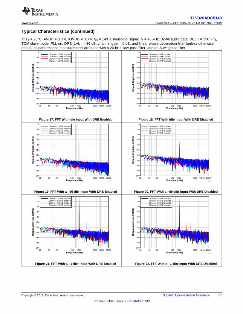
Typical Characteristics (continued)at TA = 25°C, AVDD = 3.3 V, IOVDD = 3.3 V, fIN = 1-kHz sinusoidal signal, fS = 48 kHz, 32-bit audio data, BCLK = 256 × fS,TDM slave mode, PLL on, DRE_LVL = –36 dB, channel gain = 0 dB, and linear phase decimation filter (unless otherwisenoted); all performance measurements are done with a 20-kHz, low-pass filter, and an A-weighted filter
Figure 17. FFT With Idle Input With DRE Enabled Figure 18. FFT With Idle Input With DRE Disabled
Figure 19. FFT With a –60-dBr Input With DRE Enabled Figure 20. FFT With a –60-dBr Input With DRE Disabled
Figure 21. FFT With a –1-dBr Input With DRE Enabled Figure 22. FFT With a –1-dBr Input With DRE Disabled
18
TLV320ADC5140SBAS892A –JULY 2019–REVISED OCTOBER 2019 www.ti.com
Product Folder Links: TLV320ADC5140
Submit Documentation Feedback Copyright © 2019, Texas Instruments Incorporated
8 Detailed Description
8.1 OverviewThe TLV320ADC5140 is a high-performance, low-power, flexible, quad-channel, audio analog-to-digital converter(ADC) with extensive feature integration. This device is intended for applications in voice-activated systems,professional microphones, audio conferencing, portable computing, communication, and entertainmentapplications. The high dynamic range of the device enables far-field audio recording with high fidelity. This deviceintegrates a host of features that reduces cost, board space, and power consumption in space-constrained,battery-powered, consumer, home, and industrial applications.
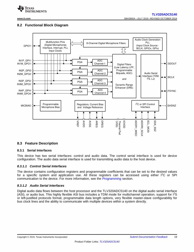
The TLV320ADC5140 consists of the following blocks:• Quad-channel, multibit, high-performance delta-sigma (ΔΣ) ADC• Configurable single-ended or differential audio inputs• Low-noise, programmable microphone bias output• Dynamic range enhancer (DRE) to support 120-dB dynamic range• Automatic gain controller (AGC)• Programmable decimation filters with linear-phase or low-latency filter• Programmable channel gain, volume control, biquad filters for each channel• Programmable phase and gain calibration with fine resolution for each channel• Programmable high-pass filter (HPF), and digital channel mixer• Pulse density modulation (PDM) digital microphone interface with high-performance decimation filter• Integrated low-jitter phase-locked loop (PLL) supporting a wide range of system clocks• Integrated digital and analog voltage regulators to support single-supply operation
Communication to the TLV320ADC5140 to configure the control registers is supported using an I2C or SPIinterface. The device supports a highly flexible audio serial interface [time-division multiplexing (TDM), I2S, orleft-justified (LJ)] to transmit audio data seamlessly in the system across devices.
The device can support multiple devices by sharing the common I2C and TDM buses across devices. Moreover,the device includes a daisy-chain feature and a secondary audio serial output data pin. These features relax theshared TDM bus timing requirements and board design complexities when operating multiple devices forapplications requiring high audio data bandwidth.
Table 1 lists the reference abbreviations used throughout this document to registers that control the device.
Table 1. Abbreviations for Register ReferencesREFERENCE ABBREVIATION DESCRIPTION EXAMPLE
Page y, register z, bit k Py_Rz_Dk Single data bit. The value of asingle bit in a register. Page 4, register 36, bit 0 = P4_R36_D0
Page y, register z, bits k-m Py_Rz_D[k:m] Range of data bits. A range ofdata bits (inclusive). Page 4, register 36, bits 3-0 = P4_R36_D[3:0]
Page y, register z Py_Rz One entire register. All eightbits in the register as a unit. Page 4, register 36 = P4_R36
Page y, registers z-n Py_Rz-Rn Range of registers. A range ofregisters in the same page. Page 4, registers 36, 37, 38 = P4_R36-R38
PGAADC
Channel-1 Digital Filters
(Low Latency LPF,
Programmable
Biquads, AGC)
and
Dynamic Range
Enhancer (DRE)
Audio Serial Interface (TDM,
I2S, LJ)
Audio Clock Generation
PLL
(Input Clock Source -
BCLK, GPIOx, GPIx)
I2C or SPI Control Interface
BCLK
FSYNC
SDOUTIN1M_GPO1
IN1P_GPI1
SC
L_M
OS
I
SD
A_S
SZ
IN2M_GPO2
IN2P_GPI2
IN3M_GPO3
IN3P_GPI3
IN4M_GPO4
IN4P_GPI4
GPIO1
Multifunction Pins
(Digital Microphones
Interface, Interrupt, PLL
Input Clock)A
DD
R0_S
CL
K
AD
DR
1_M
ISO
PGAADC
Channel-2
PGAADC
Channel-3
PGAADC
Channel-4
Programmable
Microphone BiasMICBIAS
8-Channel Digital Microphone Filters
SHDNZRegulators, Current Bias
and Voltage ReferenceA
VS
S
AV
DD
IOV
DD
DR
EG
VR
EF
Th
erm
al P
ad
(VS
S)
AR
EG
19
TLV320ADC5140www.ti.com SBAS892A –JULY 2019–REVISED OCTOBER 2019
Product Folder Links: TLV320ADC5140
Submit Documentation FeedbackCopyright © 2019, Texas Instruments Incorporated
8.2 Functional Block Diagram
8.3 Feature Description
8.3.1 Serial InterfacesThis device has two serial interfaces: control and audio data. The control serial interface is used for deviceconfiguration. The audio data serial interface is used for transmitting audio data to the host device.
8.3.1.1 Control Serial InterfacesThe device contains configuration registers and programmable coefficients that can be set to the desired valuesfor a specific system and application use. All these registers can be accessed using either I2C or SPIcommunication to the device. For more information, see the Programming section.
8.3.1.2 Audio Serial InterfacesDigital audio data flows between the host processor and the TLV320ADC5140 on the digital audio serial interface(ASI), or audio bus. This highly flexible ASI bus includes a TDM mode for multichannel operation, support for I2Sor left-justified protocols format, programmable data length options, very flexible master-slave configurability forbus clock lines and the ability to communicate with multiple devices within a system directly.
20
TLV320ADC5140SBAS892A –JULY 2019–REVISED OCTOBER 2019 www.ti.com
Product Folder Links: TLV320ADC5140
Submit Documentation Feedback Copyright © 2019, Texas Instruments Incorporated
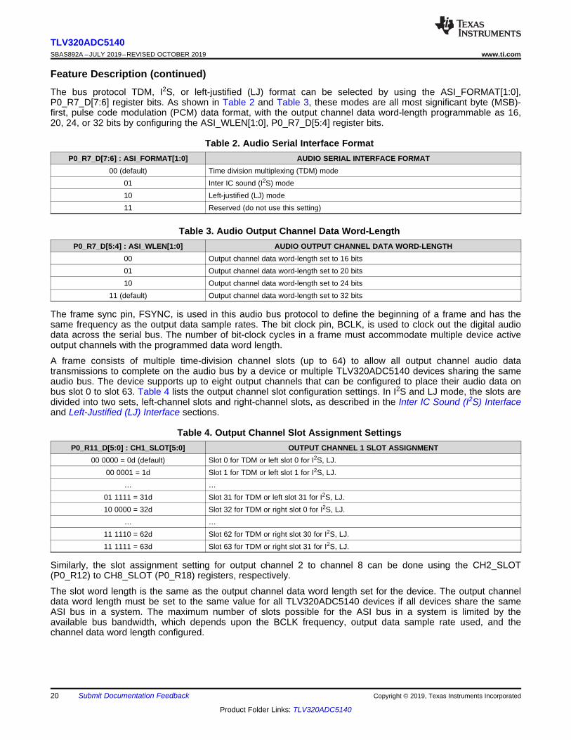
Feature Description (continued)The bus protocol TDM, I2S, or left-justified (LJ) format can be selected by using the ASI_FORMAT[1:0],P0_R7_D[7:6] register bits. As shown in Table 2 and Table 3, these modes are all most significant byte (MSB)-first, pulse code modulation (PCM) data format, with the output channel data word-length programmable as 16,20, 24, or 32 bits by configuring the ASI_WLEN[1:0], P0_R7_D[5:4] register bits.
Table 2. Audio Serial Interface FormatP0_R7_D[7:6] : ASI_FORMAT[1:0] AUDIO SERIAL INTERFACE FORMAT
00 (default) Time division multiplexing (TDM) mode01 Inter IC sound (I2S) mode10 Left-justified (LJ) mode11 Reserved (do not use this setting)
Table 3. Audio Output Channel Data Word-LengthP0_R7_D[5:4] : ASI_WLEN[1:0] AUDIO OUTPUT CHANNEL DATA WORD-LENGTH
00 Output channel data word-length set to 16 bits01 Output channel data word-length set to 20 bits10 Output channel data word-length set to 24 bits
11 (default) Output channel data word-length set to 32 bits
The frame sync pin, FSYNC, is used in this audio bus protocol to define the beginning of a frame and has thesame frequency as the output data sample rates. The bit clock pin, BCLK, is used to clock out the digital audiodata across the serial bus. The number of bit-clock cycles in a frame must accommodate multiple device activeoutput channels with the programmed data word length.
A frame consists of multiple time-division channel slots (up to 64) to allow all output channel audio datatransmissions to complete on the audio bus by a device or multiple TLV320ADC5140 devices sharing the sameaudio bus. The device supports up to eight output channels that can be configured to place their audio data onbus slot 0 to slot 63. Table 4 lists the output channel slot configuration settings. In I2S and LJ mode, the slots aredivided into two sets, left-channel slots and right-channel slots, as described in the Inter IC Sound (I2S) Interfaceand Left-Justified (LJ) Interface sections.
Table 4. Output Channel Slot Assignment SettingsP0_R11_D[5:0] : CH1_SLOT[5:0] OUTPUT CHANNEL 1 SLOT ASSIGNMENT
00 0000 = 0d (default) Slot 0 for TDM or left slot 0 for I2S, LJ.00 0001 = 1d Slot 1 for TDM or left slot 1 for I2S, LJ.
… …01 1111 = 31d Slot 31 for TDM or left slot 31 for I2S, LJ.10 0000 = 32d Slot 32 for TDM or right slot 0 for I2S, LJ.
… …11 1110 = 62d Slot 62 for TDM or right slot 30 for I2S, LJ.11 1111 = 63d Slot 63 for TDM or right slot 31 for I2S, LJ.
Similarly, the slot assignment setting for output channel 2 to channel 8 can be done using the CH2_SLOT(P0_R12) to CH8_SLOT (P0_R18) registers, respectively.
The slot word length is the same as the output channel data word length set for the device. The output channeldata word length must be set to the same value for all TLV320ADC5140 devices if all devices share the sameASI bus in a system. The maximum number of slots possible for the ASI bus in a system is limited by theavailable bus bandwidth, which depends upon the BCLK frequency, output data sample rate used, and thechannel data word length configured.
2 1 0N-1 N-1 N-2 N-3 2 1 0 N-1 N-2 N-3 2 1 0
Slot-0
(Word Length : N)
Slot-1
(Word Length : N)Slot-2 to Slot-7
(Word Length : N)
2 1 0N-1
Slot-0
(Word Length : N)
nth Sample (n+1)th SampleTX_OFFSET = 2 TX_OFFSET = 2
FSYNC
BCLK
SDOUT
N-1 2 1 0N-2 N-3 N-1 N-2 N-3 2 1 0 N-1 N-2 N-3 2 1 0
Slot-0
(Word Length : N)
Slot-1
(Word Length : N)Slot-2 to Slot-7
(Word Length : N)
N-1 2 1 0N-2 N-3
Slot-0
(Word Length : N)
FSYNC
BCLK
SDOUT
nth Sample (n+1)th Sample
21
TLV320ADC5140www.ti.com SBAS892A –JULY 2019–REVISED OCTOBER 2019
Product Folder Links: TLV320ADC5140
Submit Documentation FeedbackCopyright © 2019, Texas Instruments Incorporated
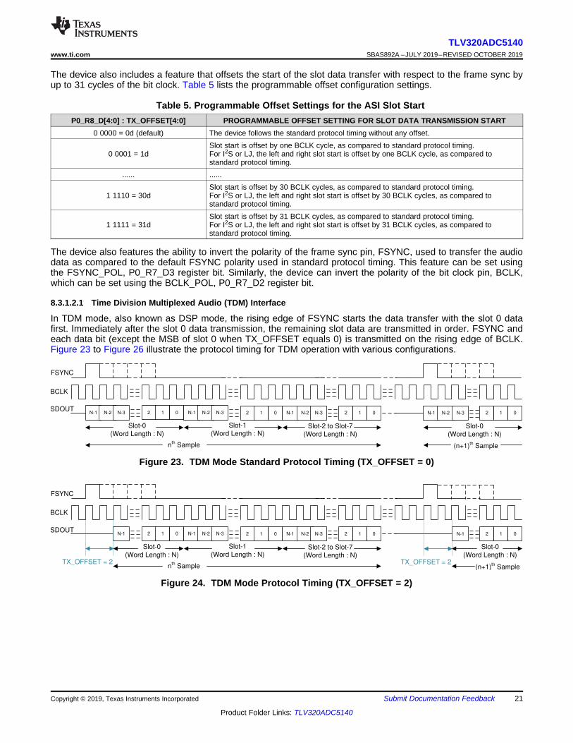
The device also includes a feature that offsets the start of the slot data transfer with respect to the frame sync byup to 31 cycles of the bit clock. Table 5 lists the programmable offset configuration settings.
Table 5. Programmable Offset Settings for the ASI Slot StartP0_R8_D[4:0] : TX_OFFSET[4:0] PROGRAMMABLE OFFSET SETTING FOR SLOT DATA TRANSMISSION START
0 0000 = 0d (default) The device follows the standard protocol timing without any offset.
0 0001 = 1dSlot start is offset by one BCLK cycle, as compared to standard protocol timing.For I2S or LJ, the left and right slot start is offset by one BCLK cycle, as compared tostandard protocol timing.
...... ......
1 1110 = 30dSlot start is offset by 30 BCLK cycles, as compared to standard protocol timing.For I2S or LJ, the left and right slot start is offset by 30 BCLK cycles, as compared tostandard protocol timing.
1 1111 = 31dSlot start is offset by 31 BCLK cycles, as compared to standard protocol timing.For I2S or LJ, the left and right slot start is offset by 31 BCLK cycles, as compared tostandard protocol timing.
The device also features the ability to invert the polarity of the frame sync pin, FSYNC, used to transfer the audiodata as compared to the default FSYNC polarity used in standard protocol timing. This feature can be set usingthe FSYNC_POL, P0_R7_D3 register bit. Similarly, the device can invert the polarity of the bit clock pin, BCLK,which can be set using the BCLK_POL, P0_R7_D2 register bit.
8.3.1.2.1 Time Division Multiplexed Audio (TDM) Interface
In TDM mode, also known as DSP mode, the rising edge of FSYNC starts the data transfer with the slot 0 datafirst. Immediately after the slot 0 data transmission, the remaining slot data are transmitted in order. FSYNC andeach data bit (except the MSB of slot 0 when TX_OFFSET equals 0) is transmitted on the rising edge of BCLK.Figure 23 to Figure 26 illustrate the protocol timing for TDM operation with various configurations.
Figure 23. TDM Mode Standard Protocol Timing (TX_OFFSET = 0)
Figure 24. TDM Mode Protocol Timing (TX_OFFSET = 2)

1 0N-1 N-2 N-1 N-2 1 0
Left
Slot-0
(Word Length : N)
Left
Slot-2 to Slot-3
(Word Length : N)
1 0N-1 N-2
FSYNC
BCLK
SDOUT
nth Sample (n+1)th Sample
1 0N-1 N-1 N-2 1 0
Right
Slot-0
(Word Length : N)
Right
Slot-2 to Slot-3
(Word Length : N)
Left
Slot-0
(Word Length : N)
N-1 2 1 0N-2 N-3 N-1 N-2 N-3 2 1 0 N-1 N-2 N-3 2 1 0
Slot-0
(Word Length : N)
Slot-1
(Word Length : N)Slot-2 to Slot-7
(Word Length : N)
N-1 2 1 0N-2 N-3
Slot-0
(Word Length : N)
FSYNC
BCLK
SDOUT
nth Sample (n+1)th Sample
nth Sample (n+1)th Sample
FSYNC
BCLK
SDOUT 2 1 0N-1 N-1 N-2 N-3 2 1 0 N-1 N-2 N-3 0 N-1 N-2
Slot-0
(Word Length : N)
Slot-1
(Word Length : N)Slot-2 to Slot-7
(Word Length : N)
2 1 0N-1
Slot-0
(Word Length : N)TX_OFFSET = 2
01 2 1 03
22
TLV320ADC5140SBAS892A –JULY 2019–REVISED OCTOBER 2019 www.ti.com
Product Folder Links: TLV320ADC5140
Submit Documentation Feedback Copyright © 2019, Texas Instruments Incorporated
Figure 25. TDM Mode Protocol Timing (No Idle BCLK Cycles, TX_OFFSET = 2)
Figure 26. TDM Mode Protocol Timing (TX_OFFSET = 0 and BCLK_POL = 1)
For proper operation of the audio bus in TDM mode, the number of bit clocks per frame must be greater than orequal to the number of active output channels times the programmed word length of the output channel data.The device supports FSYNC as a pulse with a 1-cycle-wide bit clock, but also supports multiples as well. For ahigher BCLK frequency operation, using TDM mode with a TX_OFFSET value higher than 0 is recommended.
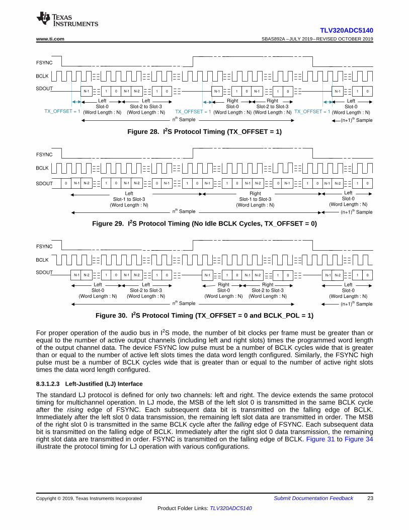
8.3.1.2.2 Inter IC Sound (I2S) Interface
The standard I2S protocol is defined for only two channels: left and right. The device extends the same protocoltiming for multichannel operation. In I2S mode, the MSB of the left slot 0 is transmitted on the falling edge ofBCLK in the second cycle after the falling edge of FSYNC. Immediately after the left slot 0 data transmission, theremaining left slot data are transmitted in order. The MSB of the right slot 0 is transmitted on the falling edge ofBCLK in the second cycle after the rising edge of FSYNC. Immediately after the right slot 0 data transmission,the remaining right slot data are transmitted in order. FSYNC and each data bit is transmitted on the falling edgeof BCLK. Figure 27 to Figure 30 illustrate the protocol timing for I2S operation with various configurations.
Figure 27. I2S Mode Standard Protocol Timing (TX_OFFSET = 0)
1 0N-1 N-2 N-1 N-2 1 0
Left
Slot-0
(Word Length : N)
Left
Slot-2 to Slot-3
(Word Length : N)
1 0N-1 N-2
FSYNC
BCLK
SDOUT
nth Sample (n+1)th Sample
1 0N-1 N-1 N-2 1 0
Right
Slot-0
(Word Length : N)
Right
Slot-2 to Slot-3
(Word Length : N)
Left
Slot-0
(Word Length : N)
1 0N-1 N-2 N-1 N-2 0 N-1
Left
Slot-1 to Slot-3
(Word Length : N)
1 0N-1 N-2
FSYNC
BCLK
SDOUT
nth Sample (n+1)th Sample
1 0N-1 0 N-1 1 0
Right
Slot-1 to Slot-3
(Word Length : N)
Left
Slot-0
(Word Length : N)
1 00 N-1 N-2
1 0N-1 N-1 N-2 1 0
Left
Slot-0
(Word Length : N)
Left
Slot-2 to Slot-3
(Word Length : N)
1 0N-1
FSYNC
BCLK
SDOUT
nth Sample (n+1)th Sample
1 0N-1 N-1 1 0
Right
Slot-0
(Word Length : N)
Right
Slot-2 to Slot-3
(Word Length : N)
Left
Slot-0
(Word Length : N)TX_OFFSET = 1 TX_OFFSET = 1 TX_OFFSET = 1
23
TLV320ADC5140www.ti.com SBAS892A –JULY 2019–REVISED OCTOBER 2019
Product Folder Links: TLV320ADC5140
Submit Documentation FeedbackCopyright © 2019, Texas Instruments Incorporated
Figure 28. I2S Protocol Timing (TX_OFFSET = 1)
Figure 29. I2S Protocol Timing (No Idle BCLK Cycles, TX_OFFSET = 0)
Figure 30. I2S Protocol Timing (TX_OFFSET = 0 and BCLK_POL = 1)
For proper operation of the audio bus in I2S mode, the number of bit clocks per frame must be greater than orequal to the number of active output channels (including left and right slots) times the programmed word lengthof the output channel data. The device FSYNC low pulse must be a number of BCLK cycles wide that is greaterthan or equal to the number of active left slots times the data word length configured. Similarly, the FSYNC highpulse must be a number of BCLK cycles wide that is greater than or equal to the number of active right slotstimes the data word length configured.
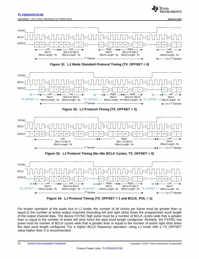
8.3.1.2.3 Left-Justified (LJ) Interface
The standard LJ protocol is defined for only two channels: left and right. The device extends the same protocoltiming for multichannel operation. In LJ mode, the MSB of the left slot 0 is transmitted in the same BCLK cycleafter the rising edge of FSYNC. Each subsequent data bit is transmitted on the falling edge of BCLK.Immediately after the left slot 0 data transmission, the remaining left slot data are transmitted in order. The MSBof the right slot 0 is transmitted in the same BCLK cycle after the falling edge of FSYNC. Each subsequent databit is transmitted on the falling edge of BCLK. Immediately after the right slot 0 data transmission, the remainingright slot data are transmitted in order. FSYNC is transmitted on the falling edge of BCLK. Figure 31 to Figure 34illustrate the protocol timing for LJ operation with various configurations.
1 0N-1 N-2 N-1 N-2 1 0
Left
Slot-0
(Word Length : N)
Left
Slot-2 to Slot-3
(Word Length : N)
1 0N-1 N-2
BCLK
SDOUT
nth Sample (n+1)th Sample
1 0N-1 N-1 N-2 1 0
Right
Slot-0
(Word Length : N)
Right
Slot-2 to Slot-3
(Word Length : N)
Left
Slot-0
(Word Length : N)
FSYNC
TX_OFFSET = 1 TX_OFFSET = 1 TX_OFFSET = 1
1 0N-1 N-2 N-1 N-2 0 N-1
Left
Slot-1 to Slot-3
(Word Length : N)
1 0N-1 N-2
BCLK
SDOUT
nth Sample (n+1)th Sample
1 0N-1 0 N-1 1 0
Right
Slot-1 to Slot-3
(Word Length : N)
Left
Slot-0
(Word Length : N)
1 00 N-1 N-2
FSYNC
1 0N-1 N-1 N-2 1 0
Left
Slot-0
(Word Length : N)
Left
Slot-2 to Slot-3
(Word Length : N)
1 0N-1
BCLK
SDOUT
nth Sample (n+1)th Sample
1 0N-1 N-1 1 0
Right
Slot-0
(Word Length : N)
Right
Slot-2 to Slot-3
(Word Length : N)
Left
Slot-0
(Word Length : N)TX_OFFSET = 2 TX_OFFSET = 2 TX_OFFSET = 2
FSYNC
1 0N-1 N-2 N-1 N-2 1 0
Left
Slot-0
(Word Length : N)
Left
Slot-2 to Slot-3
(Word Length : N)
1 0N-1 N-2
BCLK
SDOUT
nth Sample (n+1)th Sample
1 0N-1 N-1 N-2 1 0
Right
Slot-0
(Word Length : N)
Right
Slot-2 to Slot-3
(Word Length : N)
Left
Slot-0
(Word Length : N)
FSYNC
24
TLV320ADC5140SBAS892A –JULY 2019–REVISED OCTOBER 2019 www.ti.com
Product Folder Links: TLV320ADC5140
Submit Documentation Feedback Copyright © 2019, Texas Instruments Incorporated
Figure 31. LJ Mode Standard Protocol Timing (TX_OFFSET = 0)
Figure 32. LJ Protocol Timing (TX_OFFSET = 2)
Figure 33. LJ Protocol Timing (No Idle BCLK Cycles, TX_OFFSET = 0)
Figure 34. LJ Protocol Timing (TX_OFFSET = 1 and BCLK_POL = 1)
For proper operation of the audio bus in LJ mode, the number of bit clocks per frame must be greater than orequal to the number of active output channels (including left and right slots) times the programmed word lengthof the output channel data. The device FSYNC high pulse must be a number of BCLK cycles wide that is greaterthan or equal to the number of active left slots times the data word length configured. Similarly, the FSYNC lowpulse must be number of BCLK cycles wide that is greater than or equal to the number of active right slots timesthe data word length configured. For a higher BCLK frequency operation, using LJ mode with a TX_OFFSETvalue higher than 0 is recommended.
TLV320ADCx140
U4
TLV320ADCx140
U3
TLV320ADCx140
U2
TLV320ADCx140
U1Host Processor
Audio Data Bus ± TDM, I2S, LJ Interface
Control Bus ± I2C Interface
25
TLV320ADC5140www.ti.com SBAS892A –JULY 2019–REVISED OCTOBER 2019
Product Folder Links: TLV320ADC5140
Submit Documentation FeedbackCopyright © 2019, Texas Instruments Incorporated
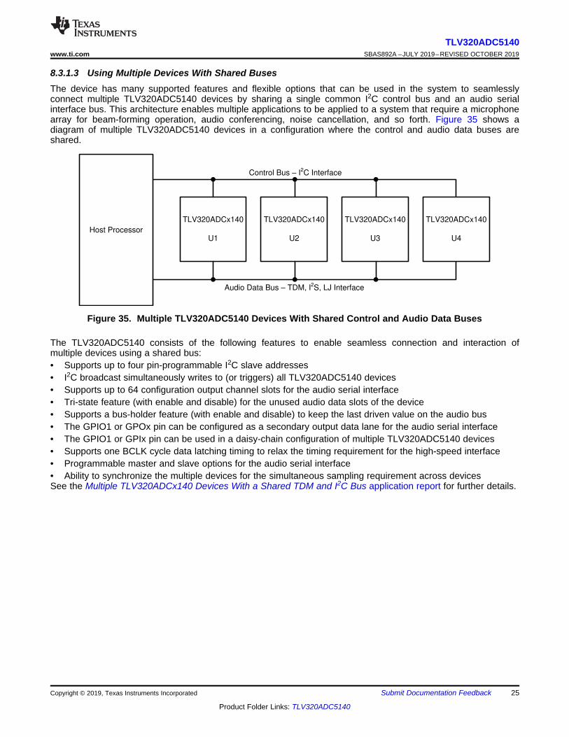
8.3.1.3 Using Multiple Devices With Shared BusesThe device has many supported features and flexible options that can be used in the system to seamlesslyconnect multiple TLV320ADC5140 devices by sharing a single common I2C control bus and an audio serialinterface bus. This architecture enables multiple applications to be applied to a system that require a microphonearray for beam-forming operation, audio conferencing, noise cancellation, and so forth. Figure 35 shows adiagram of multiple TLV320ADC5140 devices in a configuration where the control and audio data buses areshared.
Figure 35. Multiple TLV320ADC5140 Devices With Shared Control and Audio Data Buses
The TLV320ADC5140 consists of the following features to enable seamless connection and interaction ofmultiple devices using a shared bus:• Supports up to four pin-programmable I2C slave addresses• I2C broadcast simultaneously writes to (or triggers) all TLV320ADC5140 devices• Supports up to 64 configuration output channel slots for the audio serial interface• Tri-state feature (with enable and disable) for the unused audio data slots of the device• Supports a bus-holder feature (with enable and disable) to keep the last driven value on the audio bus• The GPIO1 or GPOx pin can be configured as a secondary output data lane for the audio serial interface• The GPIO1 or GPIx pin can be used in a daisy-chain configuration of multiple TLV320ADC5140 devices• Supports one BCLK cycle data latching timing to relax the timing requirement for the high-speed interface• Programmable master and slave options for the audio serial interface• Ability to synchronize the multiple devices for the simultaneous sampling requirement across devicesSee the Multiple TLV320ADCx140 Devices With a Shared TDM and I2C Bus application report for further details.
26
TLV320ADC5140SBAS892A –JULY 2019–REVISED OCTOBER 2019 www.ti.com
Product Folder Links: TLV320ADC5140
Submit Documentation Feedback Copyright © 2019, Texas Instruments Incorporated
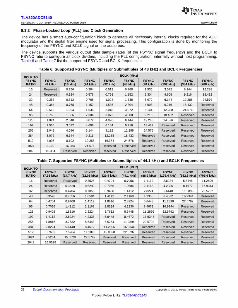
8.3.2 Phase-Locked Loop (PLL) and Clock GenerationThe device has a smart auto-configuration block to generate all necessary internal clocks required for the ADCmodulator and the digital filter engine used for signal processing. This configuration is done by monitoring thefrequency of the FSYNC and BCLK signal on the audio bus.
The device supports the various output data sample rates (of the FSYNC signal frequency) and the BCLK toFSYNC ratio to configure all clock dividers, including the PLL configuration, internally without host programming.Table 6 and Table 7 list the supported FSYNC and BCLK frequencies.
Table 6. Supported FSYNC (Multiples or Submultiples of 48 kHz) and BCLK Frequencies
BCLK TOFSYNCRATIO
BCLK (MHz)FSYNC(8 kHz)
FSYNC(16 kHz)
FSYNC(24 kHz)
FSYNC(32 kHz)
FSYNC(48 kHz)
FSYNC(96 kHz)
FSYNC(192 kHz)
FSYNC(384 kHz)
FSYNC(768 kHz)
16 Reserved 0.256 0.384 0.512 0.768 1.536 3.072 6.144 12.28824 Reserved 0.384 0.576 0.768 1.152 2.304 4.608 9.216 18.43232 0.256 0.512 0.768 1.024 1.536 3.072 6.144 12.288 24.57648 0.384 0.768 1.152 1.536 2.304 4.608 9.216 18.432 Reserved64 0.512 1.024 1.536 2.048 3.072 6.144 12.288 24.576 Reserved96 0.768 1.536 2.304 3.072 4.608 9.216 18.432 Reserved Reserved128 1.024 2.048 3.072 4.096 6.144 12.288 24.576 Reserved Reserved192 1.536 3.072 4.608 6.144 9.216 18.432 Reserved Reserved Reserved256 2.048 4.096 6.144 8.192 12.288 24.576 Reserved Reserved Reserved384 3.072 6.144 9.216 12.288 18.432 Reserved Reserved Reserved Reserved512 4.096 8.192 12.288 16.384 24.576 Reserved Reserved Reserved Reserved1024 8.192 16.384 24.576 Reserved Reserved Reserved Reserved Reserved Reserved2048 16.384 Reserved Reserved Reserved Reserved Reserved Reserved Reserved Reserved
Table 7. Supported FSYNC (Multiples or Submultiples of 44.1 kHz) and BCLK Frequencies
BCLK TOFSYNCRATIO
BCLK (MHz)FSYNC
(7.35 kHz)FSYNC
(14.7 kHz)FSYNC
(22.05 kHz)FSYNC
(29.4 kHz)FSYNC
(44.1 kHz)FSYNC
(88.2 kHz)FSYNC
(176.4 kHz)FSYNC
(352.8 kHz)FSYNC
(705.6 kHz)16 Reserved Reserved 0.3528 0.4704 0.7056 1.4112 2.8224 5.6448 11.289624 Reserved 0.3528 0.5292 0.7056 1.0584 2.1168 4.2336 8.4672 16.934432 Reserved 0.4704 0.7056 0.9408 1.4112 2.8224 5.6448 11.2896 22.579248 0.3528 0.7056 1.0584 1.4112 2.1168 4.2336 8.4672 16.9344 Reserved64 0.4704 0.9408 1.4112 1.8816 2.8224 5.6448 11.2896 22.5792 Reserved96 0.7056 1.4112 2.1168 2.8224 4.2336 8.4672 16.9344 Reserved Reserved128 0.9408 1.8816 2.8224 3.7632 5.6448 11.2896 22.5792 Reserved Reserved192 1.4112 2.8224 4.2336 5.6448 8.4672 16.9344 Reserved Reserved Reserved256 1.8816 3.7632 5.6448 7.5264 11.2896 22.5792 Reserved Reserved Reserved384 2.8224 5.6448 8.4672 11.2896 16.9344 Reserved Reserved Reserved Reserved512 3.7632 7.5264 11.2896 15.0528 22.5792 Reserved Reserved Reserved Reserved1024 7.5264 15.0528 22.5792 Reserved Reserved Reserved Reserved Reserved Reserved2048 15.0528 Reserved Reserved Reserved Reserved Reserved Reserved Reserved Reserved
27
TLV320ADC5140www.ti.com SBAS892A –JULY 2019–REVISED OCTOBER 2019
Product Folder Links: TLV320ADC5140
Submit Documentation FeedbackCopyright © 2019, Texas Instruments Incorporated
The status register ASI_STS, P0_R21, captures the device auto detect result for the FSYNC frequency and theBCLK to FSYNC ratio. If the device finds any unsupported combinations of FSYNC frequency and BCLK toFSYNC ratios, the device generates an ASI clock-error interrupt and mutes the record channels accordingly.
The device uses an integrated, low-jitter, phase-locked loop (PLL) to generate internal clocks required for theADC modulator and digital filter engine, as well as other control blocks. The device also supports an option touse BCLK, GPIO1, or the GPIx pin (as MCLK) as the audio clock source without using the PLL to reduce powerconsumption. However, the ADC performance may degrade based on jitter from the external clock source, andsome processing features may not be supported if the external audio clock source frequency is not high enough.Therefore, TI recommends using the PLL for high-performance applications. More details and information on howto configure and use the device in low-power mode without using the PLL are discussed in the TLV320ADCx140Operation for Low-Power Critical Applications application report.
The device also supports an audio bus master mode operation using the GPIO1 or GPIx pin (as MCLK) as thereference input clock source and supports various flexible options and a wide variety of system clocks. Moredetails and information on master mode configuration and operation are discussed in the Configuring andOperating the TLV320ADCx140 as an Audio Bus Master application report.
The audio bus clock error detection and auto-detect feature automatically generates all internal clocks, but canbe disabled using the ASI_ERR, P0_R9_D5 and AUTO_CLK_CFG, P0_R19_D6, register bits, respectively. Inthe system, this disable feature can be used to support custom clock frequencies that are not covered by theauto detect scheme. For such application use cases, care must be taken to ensure that the multiple clockdividers are all configured appropriately. Therefore, TI recommends using the PPC3 GUI for device configurationsettings; for more details see the TLV320ADCx140 Evaluation module user's guide and the PurePath™ consolegraphical development suite.
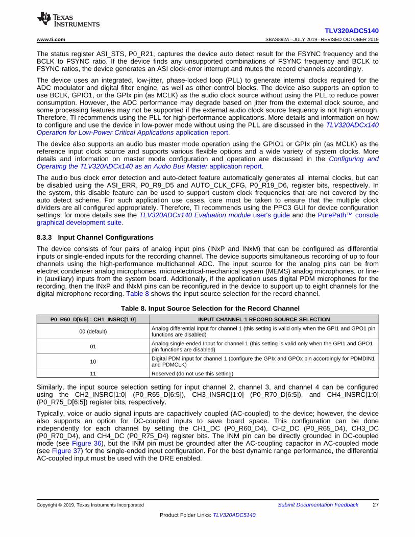
8.3.3 Input Channel ConfigurationsThe device consists of four pairs of analog input pins (INxP and INxM) that can be configured as differentialinputs or single-ended inputs for the recording channel. The device supports simultaneous recording of up to fourchannels using the high-performance multichannel ADC. The input source for the analog pins can be fromelectret condenser analog microphones, microelectrical-mechanical system (MEMS) analog microphones, or line-in (auxiliary) inputs from the system board. Additionally, if the application uses digital PDM microphones for therecording, then the INxP and INxM pins can be reconfigured in the device to support up to eight channels for thedigital microphone recording. Table 8 shows the input source selection for the record channel.
Table 8. Input Source Selection for the Record ChannelP0_R60_D[6:5] : CH1_INSRC[1:0] INPUT CHANNEL 1 RECORD SOURCE SELECTION
00 (default) Analog differential input for channel 1 (this setting is valid only when the GPI1 and GPO1 pinfunctions are disabled)
01 Analog single-ended Input for channel 1 (this setting is valid only when the GPI1 and GPO1pin functions are disabled)
10 Digital PDM input for channel 1 (configure the GPIx and GPOx pin accordingly for PDMDIN1and PDMCLK)
11 Reserved (do not use this setting)
Similarly, the input source selection setting for input channel 2, channel 3, and channel 4 can be configuredusing the CH2_INSRC[1:0] (P0_R65_D[6:5]), CH3_INSRC[1:0] (P0_R70_D[6:5]), and CH4_INSRC[1:0](P0_R75_D[6:5]) register bits, respectively.
Typically, voice or audio signal inputs are capacitively coupled (AC-coupled) to the device; however, the devicealso supports an option for DC-coupled inputs to save board space. This configuration can be doneindependently for each channel by setting the CH1_DC (P0_R60_D4), CH2_DC (P0_R65_D4), CH3_DC(P0_R70_D4), and CH4_DC (P0_R75_D4) register bits. The INM pin can be directly grounded in DC-coupledmode (see Figure 36), but the INM pin must be grounded after the AC-coupling capacitor in AC-coupled mode(see Figure 37) for the single-ended input configuration. For the best dynamic range performance, the differentialAC-coupled input must be used with the DRE enabled.

TLV320ADCx140
INxP
INxM
GND
Line or
Microphone
Single-ended
Input
GND
Line or
Microphone
Single-ended
Input
TLV320ADCx140
INxP
INxM
28
TLV320ADC5140SBAS892A –JULY 2019–REVISED OCTOBER 2019 www.ti.com
Product Folder Links: TLV320ADC5140
Submit Documentation Feedback Copyright © 2019, Texas Instruments Incorporated
Figure 36. Single-Ended DC-Coupled Input Connection Figure 37. Single-Ended AC-Coupled Input Connection
The device allows for flexibility in choosing the typical input impedance on INxP or INxM from 2.5 kΩ (default),10 kΩ, and 20 kΩ based on the input source impedance. The higher input impedance results in slightly highernoise or lower dynamic range. Table 9 lists the configuration register settings for the input impedance for therecord channel.
Table 9. Input Impedance Selection for the Record ChannelP0_R60_D[3:2] : CH1_IMP[1:0] CHANNEL 1 INPUT IMPEDANCE SELECTION
00 (default) Channel 1 input impedance typical value is 2.5 kΩ on INxP or INxM01 Channel 1 input impedance typical value is 10 kΩ on INxP or INxM10 Channel 1 input impedance typical value is 20 kΩ on INxP or INxM11 Reserved (do not use this setting)
Similarly, the input impedance selection setting for input channel 2, channel 3, and channel 4 can be configuredusing the CH2_IMP[1:0] (P0_R65_D[3:2]), CH3_IMP[1:0] (P0_R70_D[3:2]), and CH4_IMP[1:0] (P0_R75_D[3:2])register bits, respectively.
The value of the coupling capacitor in AC-coupled mode must be chosen so that the high-pass filter formed bythe coupling capacitor and the input impedance do not affect the signal content. Before proper recording canbegin, this coupling capacitor must be charged up to the common-mode voltage at power-up. To enable quickcharging, the device has modes to speed up the charging of the coupling capacitor. The default value of thequick-charge timing is set for a coupling capacitor up to 1 µF. However, if a higher-value capacitor is used in thesystem, then the quick-charging timing can be increased by using the INCAP_QCHG (P0_R5_D[5:4]) registerbits. For best distortion performance, use the low-voltage coefficient capacitors for AC coupling. The inputimpedance value of 2.5 kΩ is not supported for the DC-coupled input.
8.3.4 Reference VoltageAll audio data converters require a DC reference voltage. The TLV320ADC5140 achieves low-noise performanceby internally generating a low-noise reference voltage. This reference voltage is generated using a band-gapcircuit with high PSRR performance. This audio converter reference voltage must be filtered externally using aminimum 1-µF capacitor connected from the VREF pin to analog ground (AVSS).
The value of this reference voltage can be configured using the P0_R59_D[1:0] register bits and must be set toan appropriate value based on the desired full-scale input for the device and the AVDD supply voltage availablein the system. The default VREF value is set to 2.75 V, which in turn supports a 2-VRMS differential full-scaleinput to the device. The required minimum AVDD voltage for this mode is 3 V. Table 10 lists the various VREFsettings supported along with required AVDD range and the supported full-scale input signal for thatconfiguration.
Table 10. VREF Programmable Settings
P0_R59_D[1:0] :ADC_FSCALE[1:0]
VREF OUTPUTVOLTAGE (Same asInternal ADC VREF)
DIFFERENTIAL FULL-SCALE INPUTSUPPORTED
SINGLE-ENDED FULL-SCALE INPUTSUPPORTED
AVDD RANGEREQUIREMENT
00 (default) 2.75 V 2 VRMS 1 VRMS 3 V to 3.6 V01 2.5 V 1.818 VRMS 0.909 VRMS 2.8 V to 3.6 V10 1.375 V 1 VRMS 0.5 VRMS 1.7 V to 1.9 V11 Reserved Reserved Reserved Reserved
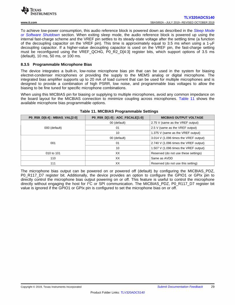
29
TLV320ADC5140www.ti.com SBAS892A –JULY 2019–REVISED OCTOBER 2019
Product Folder Links: TLV320ADC5140
Submit Documentation FeedbackCopyright © 2019, Texas Instruments Incorporated
To achieve low-power consumption, this audio reference block is powered down as described in the Sleep Modeor Software Shutdown section. When exiting sleep mode, the audio reference block is powered up using theinternal fast-charge scheme and the VREF pin settles to its steady-state voltage after the settling time (a functionof the decoupling capacitor on the VREF pin). This time is approximately equal to 3.5 ms when using a 1-μFdecoupling capacitor. If a higher-value decoupling capacitor is used on the VREF pin, the fast-charge settingmust be reconfigured using the VREF_QCHG, P0_R2_D[4:3] register bits, which support options of 3.5 ms(default), 10 ms, 50 ms, or 100 ms.
8.3.5 Programmable Microphone BiasThe device integrates a built-in, low-noise microphone bias pin that can be used in the system for biasingelectret-condenser microphones or providing the supply to the MEMS analog or digital microphone. Theintegrated bias amplifier supports up to 20 mA of load current that can be used for multiple microphones and isdesigned to provide a combination of high PSRR, low noise, and programmable bias voltages to allow thebiasing to be fine tuned for specific microphone combinations.
When using this MICBIAS pin for biasing or supplying to multiple microphones, avoid any common impedance onthe board layout for the MICBIAS connection to minimize coupling across microphones. Table 11 shows theavailable microphone bias programmable options.
Table 11. MICBIAS Programmable SettingsP0_R59_D[6:4] : MBIAS_VAL[2:0] P0_R59_D[1:0] : ADC_FSCALE[1:0] MICBIAS OUTPUT VOLTAGE
000 (default)00 (default) 2.75 V (same as the VREF output)
01 2.5 V (same as the VREF output)10 1.375 V (same as the VREF output)
00100 (default) 3.014 V (1.096 times the VREF output)
01 2.740 V (1.096 times the VREF output)10 1.507 V (1.096 times the VREF output)
010 to 101 XX Reserved (do not use these settings)110 XX Same as AVDD111 XX Reserved (do not use this setting)
The microphone bias output can be powered on or powered off (default) by configuring the MICBIAS_PDZ,P0_R117_D7 register bit. Additionally, the device provides an option to configure the GPIO1 or GPIx pin todirectly control the microphone bias output powering on or off. This feature is useful to control the microphonedirectly without engaging the host for I2C or SPI communication. The MICBIAS_PDZ, P0_R117_D7 register bitvalue is ignored if the GPIO1 or GPIx pin is configured to set the microphone bias on or off.
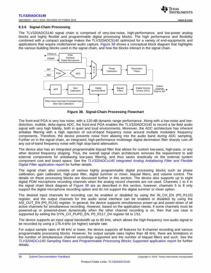
PGA
M
U
X
PDM
Interface
Digital Microphone
ADC
Phase
Calibration
Decimation
Filters
HPFGain
Calibration
Digital
Summer/Mixer
Biquad
Filters
Digital Volume
Control (DVC)
INP
INM
PDMCLK
PDMIN
Other Input Channels Processed Data
after Gain Calibration
Output
Channel
Data to ASI
30
TLV320ADC5140SBAS892A –JULY 2019–REVISED OCTOBER 2019 www.ti.com
Product Folder Links: TLV320ADC5140
Submit Documentation Feedback Copyright © 2019, Texas Instruments Incorporated
8.3.6 Signal-Chain ProcessingThe TLV320ADC5140 signal chain is comprised of very-low-noise, high-performance, and low-power analogblocks and highly flexible and programmable digital processing blocks. The high performance and flexibilitycombined with a compact package makes the TLV320ADC5140 optimized for a variety of end-equipments andapplications that require multichannel audio capture. Figure 38 shows a conceptual block diagram that highlightsthe various building blocks used in the signal chain, and how the blocks interact in the signal chain.
Figure 38. Signal-Chain Processing Flowchart
The front-end PGA is very low noise, with a 120-dB dynamic range performance. Along with a low-noise and low-distortion, multibit, delta-sigma ADC, the front-end PGA enables the TLV320ADC5140 to record a far-field audiosignal with very high fidelity, both in quiet and loud environments. Moreover, the ADC architecture has inherentantialias filtering with a high rejection of out-of-band frequency noise around multiple modulator frequencycomponents. Therefore, the device prevents noise from aliasing into the audio band during ADC sampling.Further on in the signal chain, an integrated, high-performance multistage digital decimation filter sharply cuts offany out-of-band frequency noise with high stop-band attenuation.
The device also has an integrated programmable biquad filter that allows for custom low-pass, high-pass, or anyother desired frequency shaping. Thus, the overall signal chain architecture removes the requirement to addexternal components for antialiasing low-pass filtering, and thus saves drastically on the external systemcomponent cost and board space. See the TLV320ADCx140 Integrated Analog Antialiasing Filter and FlexibleDigital Filter application report for further details.
The signal chain also consists of various highly programmable digital processing blocks such as phasecalibration, gain calibration, high-pass filter, digital summer or mixer, biquad filters, and volume control. Thedetails on these processing blocks are discussed further in this section. The device also supports up to eightdigital PDM microphone recording channels when the analog record channels are not used. Channels 1 to 4 inthe signal chain block diagram of Figure 38 are as described in this section, however, channels 5 to 8 onlysupport the digital microphone recording option and do not support the digital summer or mixer option.
The desired input channels for recording can be enabled or disabled by using the IN_CH_EN (P0_R115)register, and the output channels for the audio serial interface can be enabled or disabled by using theASI_OUT_EN (P0_R116) register. In general, the device supports simultaneous power-up and power-down of allactive channels for simultaneous recording. However, based on the application needs, if some channels must bepowered-up or powered-down dynamically when the other channel recording is on, then that use case issupported by setting the DYN_CH_PUPD_EN, P0_R117_D4 register bit to 1'b1.
The device supports an input signal bandwidth up to 80 kHz, which allows the high-frequency non-audio signal tobe recorded by using a 176.4-kHz (or higher) sample rate.
For output sample rates of 48 kHz or lower, the device supports all features for 8-channel recording and variousprogrammable processing blocks. However, for output sample rates higher than 48 kHz, there are limitations inthe number of simultaneous channel recordings supported and the number of biquad filters and such. See theTLV320ADCx140 Sampling Rates and Programmable Processing Blocks Supported application report for furtherdetails.
31
TLV320ADC5140www.ti.com SBAS892A –JULY 2019–REVISED OCTOBER 2019
Product Folder Links: TLV320ADC5140
Submit Documentation FeedbackCopyright © 2019, Texas Instruments Incorporated
8.3.6.1 Programmable Channel Gain and Digital Volume ControlThe device has an independent programmable channel gain setting for each input channel that can be set to theappropriate value based on the maximum input signal expected in the system and the ADC VREF setting used(see the Reference Voltage section), which determines the ADC full-scale signal level.
Configure the desired channel gain setting before powering up the ADC channel and do not change this settingwhile the ADC is powered on. The programmable range supported for each channel gain is from 0 dB to 42 dB insteps of 1 dB. To achieve low-noise performance, the device internal logic first maximizes the gain for the front-end low-noise analog PGA, which supports a dynamic range of 120 dB, and then applies any residualprogrammed channel gain in the digital processing block.
Table 12 shows the programmable options available for the channel gain.
Table 12. Channel Gain Programmable SettingsP0_R61_D[7:2] : CH1_GAIN[5:0] CHANNEL GAIN SETTING FOR INPUT CHANNEL 1
00 0000 = 0d (default) Input channel 1 gain is set to 0 dB00 0001 = 1d Input channel 1 gain is set to 1 dB00 0010 = 2d Input channel 1 gain is set to 2 dB
… …10 1001 = 41d Input channel 1 gain is set to 41 dB10 1010 = 42d Input channel 1 gain is set to 42 dB
10 1011 to 11 1111 = 43d to 63d Reserved (do not use these settings)
Similarly, the channel gain setting for input channel 2, channel 3, and channel 4 can be configured using theCH2_GAIN (P0_R66), CH3_GAIN (P0_R71), and CH4_GAIN (P0_R76) register bits, respectively. The channelgain feature is not available for the digital microphone record path.
The device also has a programmable digital volume control with a range from –100 dB to 27 dB in steps of0.5 dB with the option to mute the channel recording. The digital volume control value can be changeddynamically while the ADC channel is powered-up and recording. During volume control changes, the soft ramp-up or ramp-down volume feature is used internally to avoid any audible artifacts. Soft-stepping can be entirelydisabled using the DISABLE_SOFT_STEP (P0_R108_D4) register bit.
The digital volume control setting is independently available for each output channel, including the digitalmicrophone record channel. However, the device also supports an option to gang-up the volume control settingfor all channels together using the channel 1 digital volume control setting, regardless if channel 1 is powered upor powered down. This gang-up can be enabled using the DVOL_GANG (P0_R108_D7) register bit.
Table 13 shows the programmable options available for the digital volume control.
Table 13. Digital Volume Control (DVC) Programmable SettingsP0_R62_D[7:0] : CH1_DVOL[7:0] DVC SETTING FOR OUTPUT CHANNEL 1
0000 0000 = 0d Output channel 1 DVC is set to mute0000 0001 = 1d Output channel 1 DVC is set to –100 dB0000 0010 = 2d Output channel 1 DVC is set to –99.5 dB0000 0011 = 3d Output channel 1 DVC is set to –99 dB
… …1100 1000 = 200d Output channel 1 DVC is set to –0.5 dB
1100 1001 = 201d (default) Output channel 1 DVC is set to 0 dB1100 1010 = 202d Output channel 1 DVC is set to 0.5 dB
… …1111 1101 = 253d Output channel 1 DVC is set to 26 dB1111 1110 = 254d Output channel 1 DVC is set to 26.5 dB1111 1111 = 255d Output channel 1 DVC is set to 27 dB
32
TLV320ADC5140SBAS892A –JULY 2019–REVISED OCTOBER 2019 www.ti.com
Product Folder Links: TLV320ADC5140
Submit Documentation Feedback Copyright © 2019, Texas Instruments Incorporated
Similarly, the digital volume control setting for output channel 2 to channel 8 can be configured using theCH2_DVOL (P0_R67) to CH8_DVOL (P0_R97) register bits, respectively.
The internal digital processing engine soft ramps up the volume from a muted level to the programmed volumelevel when the channel is powered up, and the internal digital processing engine soft ramps down the volumefrom a programmed volume to mute when the channel is powered down. This soft-stepping of volume is done toprevent abruptly powering up and powering down the record channel. This feature can also be entirely disabledusing the DISABLE_SOFT_STEP (P0_R108_D4) register bit.
8.3.6.2 Programmable Channel Gain CalibrationAlong with the programmable channel gain and digital volume, this device also provides programmable channelgain calibration. The gain of each channel can be finely calibrated or adjusted in steps of 0.1 dB for a range of–0.8-dB to 0.7-dB gain error. This adjustment is useful when trying to match the gain across channels resultingfrom external components and microphone sensitivity. This feature, in combination with the regular digital volumecontrol, allows the gains across all channels to be matched for a wide gain error range with a resolution of0.1 dB. Table 14 shows the programmable options available for the channel gain calibration.
Table 14. Channel Gain Calibration Programmable SettingsP0_R63_D[7:4] : CH1_GCAL[3:0] CHANNEL GAIN CALIBRATION SETTING FOR INPUT CHANNEL 1
0000 = 0d Input channel 1 gain calibration is set to –0.8 dB0001 = 1d Input channel 1 gain calibration is set to –0.7 dB
… …1000 = 8d (default) Input channel 1 gain calibration is set to 0 dB
… …1110 = 14d Input channel 1 gain calibration is set to 0.6 dB1111 = 15d Input channel 1 gain calibration is set to 0.7 dB
Similarly, the channel gain calibration setting for input channel 2 to channel 8 can be configured using theCH2_GCAL (P0_R68) to CH8_GCAL (P0_R98) register bits, respectively.
8.3.6.3 Programmable Channel Phase CalibrationIn addition to the gain calibration, the phase delay in each channel can be finely calibrated or adjusted in steps ofone modulator clock cycle for a cycle range of 0 to 255 for the phase error. The modulator clock, the same clockused for ADC_MOD_CLK, is 6.144 MHz (the output data sample rate is multiples or submultiples of 48 kHz) or5.6448 MHz (the output data sample rate is multiples or submultiples of 44.1 kHz) irrespective of the analogmicrophone or digital microphone use case. This feature is very useful for many applications that must match thephase with fine resolution between each channel, including any phase mismatch across channels resulting fromexternal components or microphones. Table 15 shows the available programmable options for channel phasecalibration.
Table 15. Channel Phase Calibration Programmable SettingsP0_R64_D[7:0] : CH1_PCAL[7:0] CHANNEL PHASE CALIBRATION SETTING FOR INPUT CHANNEL 1
0000 0000 = 0d (default) Input channel 1 phase calibration with no delay0000 0001 = 1d Input channel 1 phase calibration delay is set to one cycle of the modulator clock0000 0010 = 2d Input channel 1 phase calibration delay is set to two cycles of the modulator clock
… …1111 1110 = 254d Input channel 1 phase calibration delay is set to 254 cycles of the modulator clock1111 1111 = 255d Input channel 1 phase calibration delay is set to 255 cycles of the modulator clock
Similarly, the channel phase calibration setting for input channel 2 to channel 8 can be configured using theCH2_PCAL (P0_R69) to CH8_PCAL (P0_R99) register bits, respectively.
The phase calibration feature must not be used when the analog input and PDM input are used together forsimultaneous conversion.
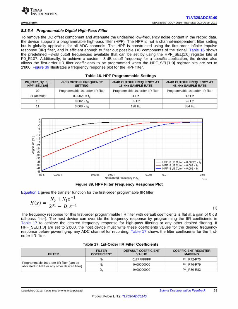
*:V; = 00 +01V
F1
231 F &1VF1
Normalized Frequency (1/fS)
Magn
itude
(dB
)
5E-5 0.0001 0.0005 0.001 0.005 0.01 0.05-45
-42
-39
-36
-33
-30
-27
-24
-21
-18
-15
-12
-9
-6
-3
0
3
D003
HPF -3 dB Cutoff = 0.00025 u fSHPF -3 dB Cutoff = 0.002 u fSHPF -3 dB Cutoff = 0.008 u fS
33
TLV320ADC5140www.ti.com SBAS892A –JULY 2019–REVISED OCTOBER 2019
Product Folder Links: TLV320ADC5140
Submit Documentation FeedbackCopyright © 2019, Texas Instruments Incorporated
8.3.6.4 Programmable Digital High-Pass FilterTo remove the DC offset component and attenuate the undesired low-frequency noise content in the record data,the device supports a programmable high-pass filter (HPF). The HPF is not a channel-independent filter settingbut is globally applicable for all ADC channels. This HPF is constructed using the first-order infinite impulseresponse (IIR) filter, and is efficient enough to filter out possible DC components of the signal. Table 16 showsthe predefined –3-dB cutoff frequencies available that can be set by using the HPF_SEL[1:0] register bits ofP0_R107. Additionally, to achieve a custom –3-dB cutoff frequency for a specific application, the device alsoallows the first-order IIR filter coefficients to be programmed when the HPF_SEL[1:0] register bits are set to2'b00. Figure 39 illustrates a frequency response plot for the HPF filter.
Table 16. HPF Programmable SettingsP0_R107_D[1:0] :
HPF_SEL[1:0]-3-dB CUTOFF FREQUENCY
SETTING-3-dB CUTOFF FREQUENCY AT
16-kHz SAMPLE RATE-3-dB CUTOFF FREQUENCY AT
48-kHz SAMPLE RATE00 Programmable 1st-order IIR filter Programmable 1st-order IIR filter Programmable 1st-order IIR filter
01 (default) 0.00025 × fS 4 Hz 12 Hz10 0.002 × fS 32 Hz 96 Hz11 0.008 × fS 128 Hz 384 Hz
Figure 39. HPF Filter Frequency Response Plot
Equation 1 gives the transfer function for the first-order programable IIR filter:
(1)
The frequency response for this first-order programmable IIR filter with default coefficients is flat at a gain of 0 dB(all-pass filter). The host device can override the frequency response by programming the IIR coefficients inTable 17 to achieve the desired frequency response for high-pass filtering or any other desired filtering. IfHPF_SEL[1:0] are set to 2'b00, the host device must write these coefficients values for the desired frequencyresponse before powering-up any ADC channel for recording. Table 17 shows the filter coefficients for the first-order IIR filter.
Table 17. 1st-Order IIR Filter Coefficients
FILTERFILTER
COEFFICIENTDEFAULT COEFFICIENT
VALUECOEFFICIENT REGISTER
MAPPING
Programmable 1st-order IIR filter (can beallocated to HPF or any other desired filter)
N0 0x7FFFFFFF P4_R72-R75N1 0x00000000 P4_R76-R79D1 0x00000000 P4_R80-R83
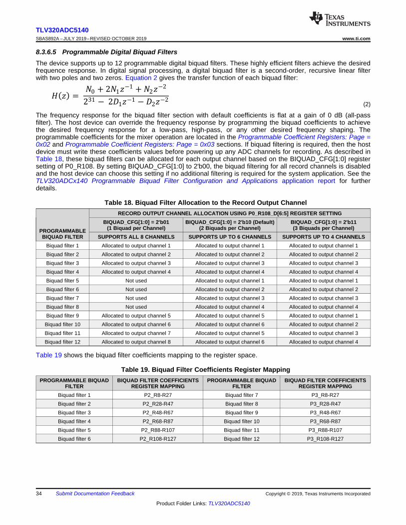
*:V; = 00 + 201V
F1+02V
F2
231 F 2&1VF1 F &2V
F2
34
TLV320ADC5140SBAS892A –JULY 2019–REVISED OCTOBER 2019 www.ti.com
Product Folder Links: TLV320ADC5140
Submit Documentation Feedback Copyright © 2019, Texas Instruments Incorporated
8.3.6.5 Programmable Digital Biquad FiltersThe device supports up to 12 programmable digital biquad filters. These highly efficient filters achieve the desiredfrequence response. In digital signal processing, a digital biquad filter is a second-order, recursive linear filterwith two poles and two zeros. Equation 2 gives the transfer function of each biquad filter:
(2)
The frequency response for the biquad filter section with default coefficients is flat at a gain of 0 dB (all-passfilter). The host device can override the frequency response by programming the biquad coefficients to achievethe desired frequency response for a low-pass, high-pass, or any other desired frequency shaping. Theprogrammable coefficients for the mixer operation are located in the Programmable Coefficient Registers: Page =0x02 and Programmable Coefficient Registers: Page = 0x03 sections. If biquad filtering is required, then the hostdevice must write these coefficients values before powering up any ADC channels for recording. As described inTable 18, these biquad filters can be allocated for each output channel based on the BIQUAD_CFG[1:0] registersetting of P0_R108. By setting BIQUAD_CFG[1:0] to 2'b00, the biquad filtering for all record channels is disabledand the host device can choose this setting if no additional filtering is required for the system application. See theTLV320ADCx140 Programmable Biquad Filter Configuration and Applications application report for furtherdetails.
Table 18. Biquad Filter Allocation to the Record Output Channel
PROGRAMMABLEBIQUAD FILTER
RECORD OUTPUT CHANNEL ALLOCATION USING P0_R108_D[6:5] REGISTER SETTINGBIQUAD_CFG[1:0] = 2'b01
(1 Biquad per Channel)BIQUAD_CFG[1:0] = 2'b10 (Default)
(2 Biquads per Channel)BIQUAD_CFG[1:0] = 2'b11(3 Biquads per Channel)
SUPPORTS ALL 8 CHANNELS SUPPORTS UP TO 6 CHANNELS SUPPORTS UP TO 4 CHANNELSBiquad filter 1 Allocated to output channel 1 Allocated to output channel 1 Allocated to output channel 1Biquad filter 2 Allocated to output channel 2 Allocated to output channel 2 Allocated to output channel 2Biquad filter 3 Allocated to output channel 3 Allocated to output channel 3 Allocated to output channel 3Biquad filter 4 Allocated to output channel 4 Allocated to output channel 4 Allocated to output channel 4Biquad filter 5 Not used Allocated to output channel 1 Allocated to output channel 1Biquad filter 6 Not used Allocated to output channel 2 Allocated to output channel 2Biquad filter 7 Not used Allocated to output channel 3 Allocated to output channel 3Biquad filter 8 Not used Allocated to output channel 4 Allocated to output channel 4Biquad filter 9 Allocated to output channel 5 Allocated to output channel 5 Allocated to output channel 1Biquad filter 10 Allocated to output channel 6 Allocated to output channel 6 Allocated to output channel 2Biquad filter 11 Allocated to output channel 7 Allocated to output channel 5 Allocated to output channel 3Biquad filter 12 Allocated to output channel 8 Allocated to output channel 6 Allocated to output channel 4
Table 19 shows the biquad filter coefficients mapping to the register space.
Table 19. Biquad Filter Coefficients Register MappingPROGRAMMABLE BIQUAD
FILTERBIQUAD FILTER COEFFICIENTS
REGISTER MAPPINGPROGRAMMABLE BIQUAD
FILTERBIQUAD FILTER COEFFICIENTS
REGISTER MAPPINGBiquad filter 1 P2_R8-R27 Biquad filter 7 P3_R8-R27Biquad filter 2 P2_R28-R47 Biquad filter 8 P3_R28-R47Biquad filter 3 P2_R48-R67 Biquad filter 9 P3_R48-R67Biquad filter 4 P2_R68-R87 Biquad filter 10 P3_R68-R87Biquad filter 5 P2_R88-R107 Biquad filter 11 P3_R88-R107Biquad filter 6 P2_R108-R127 Biquad filter 12 P3_R108-R127
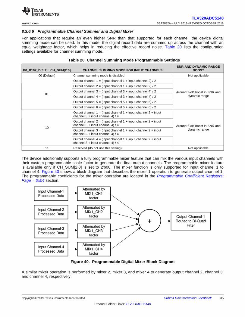
Input Channel-1
Processed Data
Input Channel-2
Processed Data
Input Channel-3
Processed Data
Input Channel-4
Processed Data
Attenuated by
MIX1_CH1factor
Attenuated by
MIX1_CH2
factor
Attenuated byMIX1_CH3
factor
Attenuated by
MIX1_CH4
factor
+Output Channel-1
Routed to Bi-Quad
Filter
35
TLV320ADC5140www.ti.com SBAS892A –JULY 2019–REVISED OCTOBER 2019
Product Folder Links: TLV320ADC5140
Submit Documentation FeedbackCopyright © 2019, Texas Instruments Incorporated
8.3.6.6 Programmable Channel Summer and Digital MixerFor applications that require an even higher SNR than that supported for each channel, the device digitalsumming mode can be used. In this mode, the digital record data are summed up across the channel with anequal weightage factor, which helps in reducing the effective record noise. Table 20 lists the configurationsettings available for channel summing mode.
Table 20. Channel Summing Mode Programmable Settings
P0_R107_D[3:2] : CH_SUM[2:0] CHANNEL SUMMING MODE FOR INPUT CHANNELSSNR AND DYNAMIC RANGE
BOOST00 (Default) Channel summing mode is disabled Not applicable
01
Output channel 1 = (input channel 1 + input channel 2) / 2
Around 3-dB boost in SNR anddynamic range
Output channel 2 = (input channel 1 + input channel 2) / 2Output channel 3 = (input channel 3 + input channel 4) / 2Output channel 4 = (input channel 3 + input channel 4) / 2Output channel 5 = (input channel 5 + input channel 6) / 2Output channel 6 = (input channel 5 + input channel 6) / 2
10
Output channel 1 = (input channel 1 + input channel 2 + inputchannel 3 + input channel 4) / 4
Around 6-dB boost in SNR anddynamic range
Output channel 2 = (input channel 1 + input channel 2 + inputchannel 3 + input channel 4) / 4Output channel 3 = (input channel 1 + input channel 2 + inputchannel 3 + input channel 4) / 4Output channel 4 = (input channel 1 + input channel 2 + inputchannel 3 + input channel 4) / 4
11 Reserved (do not use this setting) Not applicable
The device additionally supports a fully programmable mixer feature that can mix the various input channels withtheir custom programmable scale factor to generate the final output channels. The programmable mixer featureis available only if CH_SUM[2:0] is set to 2'b00. The mixer function is only supported for input channel 1 tochannel 4. Figure 40 shows a block diagram that describes the mixer 1 operation to generate output channel 1.The programmable coefficients for the mixer operation are located in the Programmable Coefficient Registers:Page = 0x04 section.
Figure 40. Programmable Digital Mixer Block Diagram
A similar mixer operation is performed by mixer 2, mixer 3, and mixer 4 to generate output channel 2, channel 3,and channel 4, respectively.
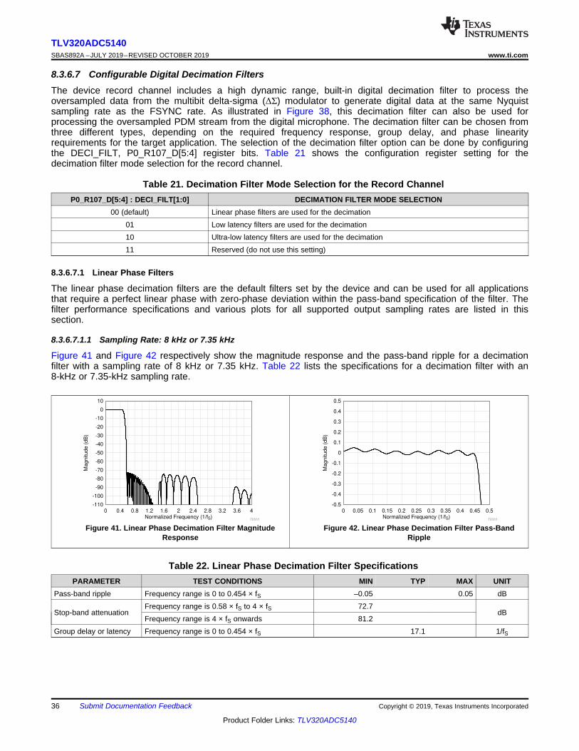
Normalized Frequency (1/fS)
Magnitude (
dB
)
0 0.4 0.8 1.2 1.6 2 2.4 2.8 3.2 3.6 4-110
-100
-90
-80
-70
-60
-50
-40
-30
-20
-10
0
10
D001Normalized Frequency (1/fS)
Magnitude (
dB
)
0 0.05 0.1 0.15 0.2 0.25 0.3 0.35 0.4 0.45 0.5-0.5
-0.4
-0.3
-0.2
-0.1
0
0.1
0.2
0.3
0.4
0.5
D001
36
TLV320ADC5140SBAS892A –JULY 2019–REVISED OCTOBER 2019 www.ti.com
Product Folder Links: TLV320ADC5140
Submit Documentation Feedback Copyright © 2019, Texas Instruments Incorporated
8.3.6.7 Configurable Digital Decimation FiltersThe device record channel includes a high dynamic range, built-in digital decimation filter to process theoversampled data from the multibit delta-sigma (ΔΣ) modulator to generate digital data at the same Nyquistsampling rate as the FSYNC rate. As illustrated in Figure 38, this decimation filter can also be used forprocessing the oversampled PDM stream from the digital microphone. The decimation filter can be chosen fromthree different types, depending on the required frequency response, group delay, and phase linearityrequirements for the target application. The selection of the decimation filter option can be done by configuringthe DECI_FILT, P0_R107_D[5:4] register bits. Table 21 shows the configuration register setting for thedecimation filter mode selection for the record channel.
Table 21. Decimation Filter Mode Selection for the Record ChannelP0_R107_D[5:4] : DECI_FILT[1:0] DECIMATION FILTER MODE SELECTION
00 (default) Linear phase filters are used for the decimation01 Low latency filters are used for the decimation10 Ultra-low latency filters are used for the decimation11 Reserved (do not use this setting)
8.3.6.7.1 Linear Phase Filters
The linear phase decimation filters are the default filters set by the device and can be used for all applicationsthat require a perfect linear phase with zero-phase deviation within the pass-band specification of the filter. Thefilter performance specifications and various plots for all supported output sampling rates are listed in thissection.
8.3.6.7.1.1 Sampling Rate: 8 kHz or 7.35 kHz
Figure 41 and Figure 42 respectively show the magnitude response and the pass-band ripple for a decimationfilter with a sampling rate of 8 kHz or 7.35 kHz. Table 22 lists the specifications for a decimation filter with an8-kHz or 7.35-kHz sampling rate.
Figure 41. Linear Phase Decimation Filter MagnitudeResponse
Figure 42. Linear Phase Decimation Filter Pass-BandRipple
Table 22. Linear Phase Decimation Filter SpecificationsPARAMETER TEST CONDITIONS MIN TYP MAX UNIT
Pass-band ripple Frequency range is 0 to 0.454 × fS –0.05 0.05 dB
Stop-band attenuationFrequency range is 0.58 × fS to 4 × fS 72.7
dBFrequency range is 4 × fS onwards 81.2
Group delay or latency Frequency range is 0 to 0.454 × fS 17.1 1/fS
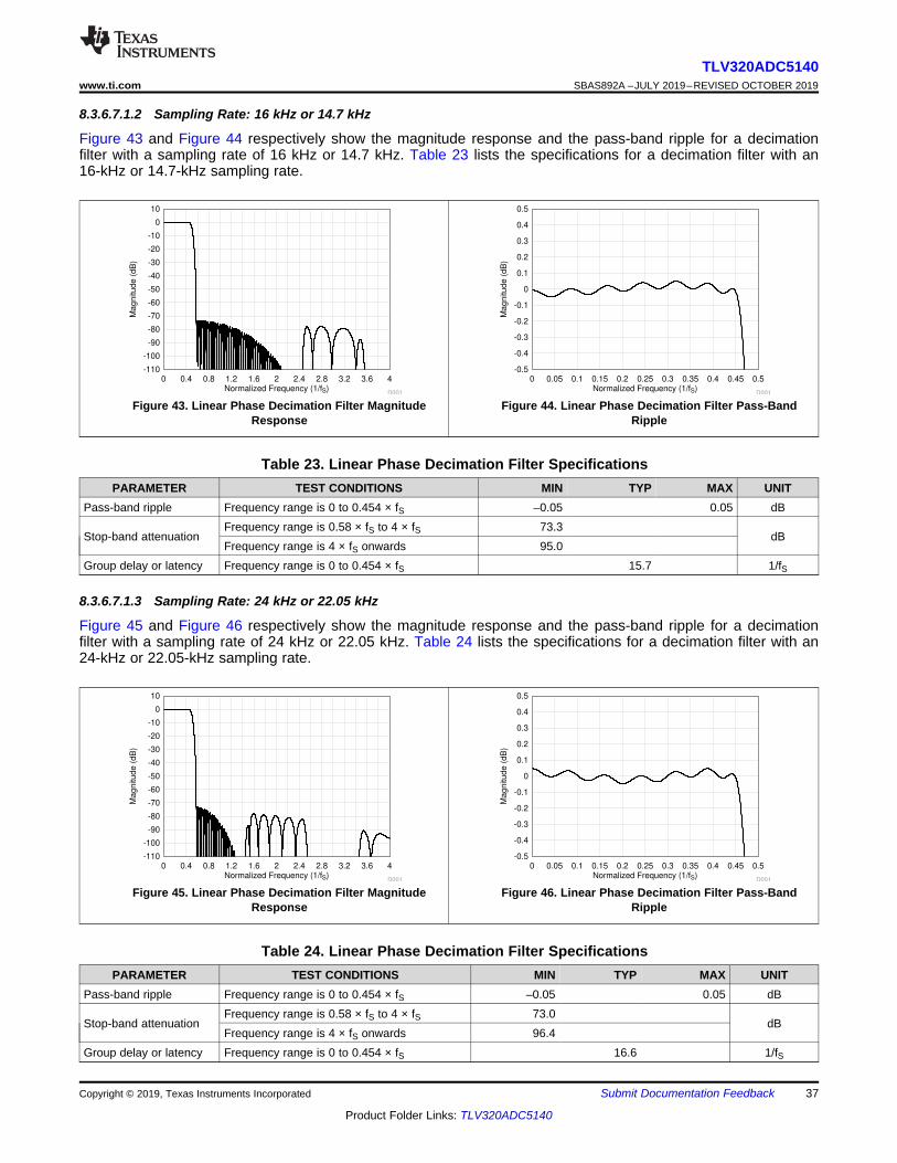
Normalized Frequency (1/fS)
Magnitude (
dB
)
0 0.4 0.8 1.2 1.6 2 2.4 2.8 3.2 3.6 4-110
-100
-90
-80
-70
-60
-50
-40
-30
-20
-10
0
10
D001Normalized Frequency (1/fS)
Magnitude (
dB
)
0 0.05 0.1 0.15 0.2 0.25 0.3 0.35 0.4 0.45 0.5-0.5
-0.4
-0.3
-0.2
-0.1
0
0.1
0.2
0.3
0.4
0.5
D001
Normalized Frequency (1/fS)
Magnitude (
dB
)
0 0.4 0.8 1.2 1.6 2 2.4 2.8 3.2 3.6 4-110
-100
-90
-80
-70
-60
-50
-40
-30
-20
-10
0
10
D001Normalized Frequency (1/fS)
Magnitude (
dB
)
0 0.05 0.1 0.15 0.2 0.25 0.3 0.35 0.4 0.45 0.5-0.5
-0.4
-0.3
-0.2
-0.1
0
0.1
0.2
0.3
0.4
0.5
D001
37
TLV320ADC5140www.ti.com SBAS892A –JULY 2019–REVISED OCTOBER 2019
Product Folder Links: TLV320ADC5140
Submit Documentation FeedbackCopyright © 2019, Texas Instruments Incorporated
8.3.6.7.1.2 Sampling Rate: 16 kHz or 14.7 kHz
Figure 43 and Figure 44 respectively show the magnitude response and the pass-band ripple for a decimationfilter with a sampling rate of 16 kHz or 14.7 kHz. Table 23 lists the specifications for a decimation filter with an16-kHz or 14.7-kHz sampling rate.
Figure 43. Linear Phase Decimation Filter MagnitudeResponse
Figure 44. Linear Phase Decimation Filter Pass-BandRipple
Table 23. Linear Phase Decimation Filter SpecificationsPARAMETER TEST CONDITIONS MIN TYP MAX UNIT
Pass-band ripple Frequency range is 0 to 0.454 × fS –0.05 0.05 dB
Stop-band attenuationFrequency range is 0.58 × fS to 4 × fS 73.3
dBFrequency range is 4 × fS onwards 95.0
Group delay or latency Frequency range is 0 to 0.454 × fS 15.7 1/fS
8.3.6.7.1.3 Sampling Rate: 24 kHz or 22.05 kHz
Figure 45 and Figure 46 respectively show the magnitude response and the pass-band ripple for a decimationfilter with a sampling rate of 24 kHz or 22.05 kHz. Table 24 lists the specifications for a decimation filter with an24-kHz or 22.05-kHz sampling rate.
Figure 45. Linear Phase Decimation Filter MagnitudeResponse
Figure 46. Linear Phase Decimation Filter Pass-BandRipple
Table 24. Linear Phase Decimation Filter SpecificationsPARAMETER TEST CONDITIONS MIN TYP MAX UNIT
Pass-band ripple Frequency range is 0 to 0.454 × fS –0.05 0.05 dB
Stop-band attenuationFrequency range is 0.58 × fS to 4 × fS 73.0
dBFrequency range is 4 × fS onwards 96.4
Group delay or latency Frequency range is 0 to 0.454 × fS 16.6 1/fS
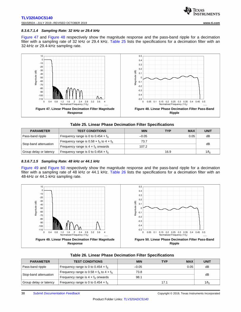
Normalized Frequency (1/fS)
Magnitude (
dB
)
0 0.4 0.8 1.2 1.6 2 2.4 2.8 3.2 3.6 4-110
-100
-90
-80
-70
-60
-50
-40
-30
-20
-10
0
10
D001Normalized Frequency (1/fS)
Magnitude (
dB
)
0 0.05 0.1 0.15 0.2 0.25 0.3 0.35 0.4 0.45 0.5-0.5
-0.4
-0.3
-0.2
-0.1
0
0.1
0.2
0.3
0.4
0.5
D001
Normalized Frequency (1/fS)
Magnitude (
dB
)
0 0.4 0.8 1.2 1.6 2 2.4 2.8 3.2 3.6 4-110
-100
-90
-80
-70
-60
-50
-40
-30
-20
-10
0
10
D001Normalized Frequency (1/fS)
Magnitude (
dB
)
0 0.05 0.1 0.15 0.2 0.25 0.3 0.35 0.4 0.45 0.5-0.5
-0.4
-0.3
-0.2
-0.1
0
0.1
0.2
0.3
0.4
0.5
D001
38
TLV320ADC5140SBAS892A –JULY 2019–REVISED OCTOBER 2019 www.ti.com
Product Folder Links: TLV320ADC5140
Submit Documentation Feedback Copyright © 2019, Texas Instruments Incorporated
8.3.6.7.1.4 Sampling Rate: 32 kHz or 29.4 kHz
Figure 47 and Figure 48 respectively show the magnitude response and the pass-band ripple for a decimationfilter with a sampling rate of 32 kHz or 29.4 kHz. Table 25 lists the specifications for a decimation filter with an32-kHz or 29.4-kHz sampling rate.
Figure 47. Linear Phase Decimation Filter MagnitudeResponse
Figure 48. Linear Phase Decimation Filter Pass-BandRipple
Table 25. Linear Phase Decimation Filter SpecificationsPARAMETER TEST CONDITIONS MIN TYP MAX UNIT
Pass-band ripple Frequency range is 0 to 0.454 × fS –0.05 0.05 dB
Stop-band attenuationFrequency range is 0.58 × fS to 4 × fS 73.7
dBFrequency range is 4 × fS onwards 107.2
Group delay or latency Frequency range is 0 to 0.454 × fS 16.9 1/fS
8.3.6.7.1.5 Sampling Rate: 48 kHz or 44.1 kHz
Figure 49 and Figure 50 respectively show the magnitude response and the pass-band ripple for a decimationfilter with a sampling rate of 48 kHz or 44.1 kHz. Table 26 lists the specifications for a decimation filter with an48-kHz or 44.1-kHz sampling rate.
Figure 49. Linear Phase Decimation Filter MagnitudeResponse
Figure 50. Linear Phase Decimation Filter Pass-BandRipple
Table 26. Linear Phase Decimation Filter SpecificationsPARAMETER TEST CONDITIONS MIN TYP MAX UNIT
Pass-band ripple Frequency range is 0 to 0.454 × fS –0.05 0.05 dB
Stop-band attenuationFrequency range is 0.58 × fS to 4 × fS 73.8
dBFrequency range is 4 × fS onwards 98.1
Group delay or latency Frequency range is 0 to 0.454 × fS 17.1 1/fS
Normalized Frequency (1/fS)
Magnitude (
dB
)
0 0.4 0.8 1.2 1.6 2 2.4 2.8 3.2 3.6 4-110
-100
-90
-80
-70
-60
-50
-40
-30
-20
-10
0
10
D001Normalized Frequency (1/fS)
Magnitude (
dB
)
0 0.05 0.1 0.15 0.2 0.25 0.3 0.35 0.4-0.5
-0.4
-0.3
-0.2
-0.1
0
0.1
0.2
0.3
0.4
0.5
D001
Normalized Frequency (1/fS)
Magnitude (
dB
)
0 0.4 0.8 1.2 1.6 2 2.4 2.8 3.2 3.6 4-110
-100
-90
-80
-70
-60
-50
-40
-30
-20
-10
0
10
D001Normalized Frequency (1/fS)
Magnitude (
dB
)
0 0.05 0.1 0.15 0.2 0.25 0.3 0.35 0.4 0.45 0.5-0.5
-0.4
-0.3
-0.2
-0.1
0
0.1
0.2
0.3
0.4
0.5
D001
39
TLV320ADC5140www.ti.com SBAS892A –JULY 2019–REVISED OCTOBER 2019
Product Folder Links: TLV320ADC5140
Submit Documentation FeedbackCopyright © 2019, Texas Instruments Incorporated
8.3.6.7.1.6 Sampling Rate: 96 kHz or 88.2 kHz
Figure 51 and Figure 52 respectively show the magnitude response and the pass-band ripple for a decimationfilter with a sampling rate of 96 kHz or 88.2 kHz. Table 27 lists the specifications for a decimation filter with an96-kHz or 88.2-kHz sampling rate.
Figure 51. Linear Phase Decimation Filter MagnitudeResponse
Figure 52. Linear Phase Decimation Filter Pass-BandRipple
Table 27. Linear Phase Decimation Filter SpecificationsPARAMETER TEST CONDITIONS MIN TYP MAX UNIT
Pass-band ripple Frequency range is 0 to 0.454 × fS –0.05 0.05 dB
Stop-band attenuationFrequency range is 0.58 × fS to 4 × fS 73.6
dBFrequency range is 4 × fS onwards 97.9
Group delay or latency Frequency range is 0 to 0.454 × fS 17.1 1/fS
8.3.6.7.1.7 Sampling Rate: 192 kHz or 176.4 kHz
Figure 53 and Figure 54 respectively show the magnitude response and the pass-band ripple for a decimationfilter with a sampling rate of 192 kHz or 176.4 kHz. Table 28 lists the specifications for a decimation filter with an192-kHz or 176.4-kHz sampling rate.
Figure 53. Linear Phase Decimation Filter MagnitudeResponse
Figure 54. Linear Phase Decimation Filter Pass-BandRipple
Table 28. Linear Phase Decimation Filter SpecificationsPARAMETER TEST CONDITIONS MIN TYP MAX UNIT
Pass-band ripple Frequency range is 0 to 0.3 × fS –0.05 0.05 dB
Stop-band attenuationFrequency range is 0.473 × fS to 4 × fS 70.0
dBFrequency range is 4 × fS onwards 111.0
Group delay or latency Frequency range is 0 to 0.3 × fS 11.9 1/fS
Normalized Frequency (1/fS)
Magnitude (
dB
)
0 0.4 0.8 1.2 1.6 2 2.4 2.8 3.2 3.6 4-110
-100
-90
-80
-70
-60
-50
-40
-30
-20
-10
0
10
D001Normalized Frequency (1/fS)
Magnitude (
dB
)
0 0.05 0.1 0.15 0.2-0.5
-0.4
-0.3
-0.2
-0.1
0
0.1
0.2
0.3
0.4
0.5
D001
Normalized Frequency (1/fS)
Magnitude (
dB
)
0 0.4 0.8 1.2 1.6 2 2.4 2.8 3.2 3.6 4-110
-100
-90
-80
-70
-60
-50
-40
-30
-20
-10
0
10
D001Normalized Frequency (1/fS)
Magnitude (
dB
)
0 0.05 0.1 0.15 0.2 0.25 0.3-0.5
-0.4
-0.3
-0.2
-0.1
0
0.1
0.2
0.3
0.4
0.5
D001
40
TLV320ADC5140SBAS892A –JULY 2019–REVISED OCTOBER 2019 www.ti.com
Product Folder Links: TLV320ADC5140
Submit Documentation Feedback Copyright © 2019, Texas Instruments Incorporated
8.3.6.7.1.8 Sampling Rate: 384 kHz or 352.8 kHz
Figure 55 and Figure 56 respectively show the magnitude response and the pass-band ripple for a decimationfilter with a sampling rate of 384 kHz or 352.8 kHz. Table 29 lists the specifications for a decimation filter with an384-kHz or 352.8-kHz sampling rate.
Figure 55. Linear Phase Decimation Filter MagnitudeResponse
Figure 56. Linear Phase Decimation Filter Pass-BandRipple
Table 29. Linear Phase Decimation Filter SpecificationsPARAMETER TEST CONDITIONS MIN TYP MAX UNIT
Pass-band ripple Frequency range is 0 to 0.212 × fS –0.05 0.05 dB
Stop-band attenuationFrequency range is 0.58 × fS to 4 × fS 70.0
dBFrequency range is 4 × fS onwards 108.8
Group delay or latency Frequency range is 0 to 0.212 × fS 7.2 1/fS
8.3.6.7.1.9 Sampling Rate 768 kHz or 705.6 kHz
Figure 57 and Figure 58 respectively show the magnitude response and the pass-band ripple for a decimationfilter with a sampling rate of 768 kHz or 705.6 kHz. Table 30 lists the specifications for a decimation filter with an768-kHz or 705.6-kHz sampling rate.
Figure 57. Linear Phase Decimation Filter MagnitudeResponse
Figure 58. Linear Phase Decimation Filter Pass-BandRipple
Table 30. Linear Phase Decimation Filter SpecificationsPARAMETER TEST CONDITIONS MIN TYP MAX UNIT
Pass-band ripple Frequency range is 0 to 0.113 × fS –0.05 0.05 dB
Stop-band attenuationFrequency range is 0.58 × fS to 2 × fS 75.0
dBFrequency range is 2 × fS onwards 88.0
Group Delay or Latency Frequency range is 0 to 0.113 × fS 5.9 1/fS
Normalized Frequency (1/fS)
Magn
itude
(dB
)
0 0.4 0.8 1.2 1.6 2 2.4 2.8 3.2 3.6 4-110
-100
-90
-80
-70
-60
-50
-40
-30
-20
-10
0
10
D002
Normalized Frequency (1/fS)
Magnitude (
dB
)
Phase D
evia
tion fro
m L
inear
(Degre
e)
0 0.05 0.1 0.15 0.2 0.25 0.3 0.35 0.4 0.45 0.5-0.5 -0.5
-0.4 -0.4
-0.3 -0.3
-0.2 -0.2
-0.1 -0.1
0 0
0.1 0.1
0.2 0.2
0.3 0.3
0.4 0.4
0.5 0.5
D002
Pass-Band RipplePhase Deviation
41
TLV320ADC5140www.ti.com SBAS892A –JULY 2019–REVISED OCTOBER 2019
Product Folder Links: TLV320ADC5140
Submit Documentation FeedbackCopyright © 2019, Texas Instruments Incorporated
8.3.6.7.2 Low-Latency Filters
For applications where low latency with minimal phase deviation (within the audio band) is critical, the low-latency decimation filters on the TLV320ADC5140 can be used. The device supports these filters with a groupdelay of approximately seven samples with an almost linear phase response within the 0.365 × fS frequencyband. This section provides the filter performance specifications and various plots for all supported outputsampling rates for the low-latency filters.
8.3.6.7.2.1 Sampling Rate: 16 kHz or 14.7 kHz
Figure 59 shows the magnitude response and Figure 60 shows the pass-band ripple and phase deviation for adecimation filter with a sampling rate of 16 kHz or 14.7 kHz. Table 31 lists the specifications for a decimationfilter with a 16-kHz or 14.7-kHz sampling rate.
Figure 59. Low-Latency Decimation Filter MagnitudeResponse
Figure 60. Low-Latency Decimation Filter Pass-BandRipple and Phase Deviation
Table 31. Low-Latency Decimation Filter SpecificationsPARAMETER TEST CONDITIONS MIN TYP MAX UNIT
Pass-band ripple Frequency range is 0 to 0.451 × fS –0.05 0.05 dBStop-band attenuation Frequency range is 0.61 × fS onwards 87.3 dBGroup delay or latency Frequency range is 0 to 0.363 × fS 7.6 1/fSGroup delay deviation Frequency range is 0 to 0.363 × fS –0.022 0.022 1/fSPhase deviation Frequency range is 0 to 0.363 × fS –0.21 0.25 Degrees
Normalized Frequency (1/fS)
Magn
itude
(dB
)
0 0.4 0.8 1.2 1.6 2 2.4 2.8 3.2 3.6 4-110
-100
-90
-80
-70
-60
-50
-40
-30
-20
-10
0
10
D002
Normalized Frequency (1/fS)
Magnitude (
dB
)
Phase D
evia
tion fro
m L
inear
(Degre
e)
0 0.05 0.1 0.15 0.2 0.25 0.3 0.35 0.4 0.45 0.5-0.5 -0.5
-0.4 -0.4
-0.3 -0.3
-0.2 -0.2
-0.1 -0.1
0 0
0.1 0.1
0.2 0.2
0.3 0.3
0.4 0.4
0.5 0.5
D002
Pass-Band RipplePhase Deviation
Normalized Frequency (1/fS)
Magn
itude
(dB
)
0 0.4 0.8 1.2 1.6 2 2.4 2.8 3.2 3.6 4-110
-100
-90
-80
-70
-60
-50
-40
-30
-20
-10
0
10
D002
Normalized Frequency (1/fS)
Magnitude (
dB
)
Phase D
evia
tion fro
m L
inear
(Degre
e)
0 0.05 0.1 0.15 0.2 0.25 0.3 0.35 0.4 0.45 0.5-0.5 -0.5
-0.4 -0.4
-0.3 -0.3
-0.2 -0.2
-0.1 -0.1
0 0
0.1 0.1
0.2 0.2
0.3 0.3
0.4 0.4
0.5 0.5
D002
Pass-Band RipplePhase Deviation
42
TLV320ADC5140SBAS892A –JULY 2019–REVISED OCTOBER 2019 www.ti.com
Product Folder Links: TLV320ADC5140
Submit Documentation Feedback Copyright © 2019, Texas Instruments Incorporated
8.3.6.7.2.2 Sampling Rate: 24 kHz or 22.05 kHz
Figure 61 shows the magnitude response and Figure 62 shows the pass-band ripple and phase deviation for adecimation filter with a sampling rate of 24 kHz or 22.05 kHz. Table 32 lists the specifications for a decimationfilter with a 24-kHz or 22.05-kHz sampling rate.
Figure 61. Low-Latency Decimation Filter MagnitudeResponse
Figure 62. Low-Latency Decimation Filter Pass-BandRipple and Phase Deviation
Table 32. Low-Latency Decimation Filter SpecificationsPARAMETER TEST CONDITIONS MIN TYP MAX UNIT
Pass-band ripple Frequency range is 0 to 0.459 × fS –0.01 0.01 dBStop-band attenuation Frequency range is 0.6 × fS onwards 87.2 dBGroup delay or latency Frequency range is 0 to 0.365 × fS 7.5 1/fSGroup delay deviation Frequency range is 0 to 0.365 × fS –0.026 0.026 1/fSPhase deviation Frequency range is 0 to 0.365 × fS –0.26 0.30 Degrees
8.3.6.7.2.3 Sampling Rate: 32 kHz or 29.4 kHz
Figure 63 shows the magnitude response and Figure 64 shows the pass-band ripple and phase deviation for adecimation filter with a sampling rate of 32 kHz or 29.4 kHz. Table 33 lists the specifications for a decimationfilter with a 32-kHz or 29.4-kHz sampling rate.
Figure 63. Low-Latency Decimation Filter MagnitudeResponse
Figure 64. Low-Latency Decimation Filter Pass-BandRipple and Phase Deviation

Normalized Frequency (1/fS)
Magn
itude
(dB
)
0 0.4 0.8 1.2 1.6 2 2.4 2.8 3.2 3.6 4-110
-100
-90
-80
-70
-60
-50
-40
-30
-20
-10
0
10
D002
Normalized Frequency (1/fS)
Magnitude (
dB
)
Phase D
evia
tion fro
m L
inear
(Degre
e)
0 0.05 0.1 0.15 0.2 0.25 0.3 0.35 0.4 0.45 0.5-0.5 -0.5
-0.4 -0.4
-0.3 -0.3
-0.2 -0.2
-0.1 -0.1
0 0
0.1 0.1
0.2 0.2
0.3 0.3
0.4 0.4
0.5 0.5
D002
Pass-Band RipplePhase Deviation
43
TLV320ADC5140www.ti.com SBAS892A –JULY 2019–REVISED OCTOBER 2019
Product Folder Links: TLV320ADC5140
Submit Documentation FeedbackCopyright © 2019, Texas Instruments Incorporated
Table 33. Low-Latency Decimation Filter SpecificationsPARAMETER TEST CONDITIONS MIN TYP MAX UNIT
Pass-band ripple Frequency range is 0 to 0.457 × fS –0.04 0.04 dBStop-band attenuation Frequency range is 0.6 × fS onwards 88.3 dBGroup delay or latency Frequency range is 0 to 0.368 × fS 8.7 1/fSGroup delay deviation Frequency range is 0 to 0.368 × fS –0.026 0.026 1/fSPhase deviation Frequency range is 0 to 0.368 × fS –0.26 0.31 Degrees
8.3.6.7.2.4 Sampling Rate: 48 kHz or 44.1 kHz
Figure 65 shows the magnitude response and Figure 66 shows the pass-band ripple and phase deviation for adecimation filter with a sampling rate of 48 kHz or 44.1 kHz. Table 34 lists the specifications for a decimationfilter with a 48-kHz or 44.1-kHz sampling rate.
Figure 65. Low-Latency Decimation Filter MagnitudeResponse
Figure 66. Low-Latency Decimation Filter Pass-BandRipple and Phase Deviation
Table 34. Low-Latency Decimation Filter SpecificationsPARAMETER TEST CONDITIONS MIN TYP MAX UNIT
Pass-band ripple Frequency range is 0 to 0.452 × fS –0.015 0.015 dBStop-band attenuation Frequency range is 0.6 × fS onwards 86.4 dBGroup delay or latency Frequency range is 0 to 0.365 × fS 7.7 1/fSGroup delay deviation Frequency range is 0 to 0.365 × fS –0.027 0.027 1/fSPhase deviation Frequency range is 0 to 0.365 × fS –0.25 0.30 Degrees
Normalized Frequency (1/fS)
Magn
itude
(dB
)
0 0.4 0.8 1.2 1.6 2 2.4 2.8 3.2 3.6 4-110
-100
-90
-80
-70
-60
-50
-40
-30
-20
-10
0
10
D002
Normalized Frequency (1/fS)
Magnitude (
dB
)
Phase D
evia
tion fro
m L
inear
(Degre
e)
0 0.05 0.1 0.15 0.2 0.25 0.3 0.35 0.4 0.45 0.5-0.5 -0.5
-0.4 -0.4
-0.3 -0.3
-0.2 -0.2
-0.1 -0.1
0 0
0.1 0.1
0.2 0.2
0.3 0.3
0.4 0.4
0.5 0.5
D002
Pass-Band RipplePhase Deviation
Normalized Frequency (1/fS)
Magn
itude
(dB
)
0 0.4 0.8 1.2 1.6 2 2.4 2.8 3.2 3.6 4-110
-100
-90
-80
-70
-60
-50
-40
-30
-20
-10
0
10
D002
Normalized Frequency (1/fS)
Magnitude (
dB
)
Phase D
evia
tion fro
m L
inear
(Degre
e)
0 0.05 0.1 0.15 0.2 0.25 0.3 0.35 0.4 0.45 0.5-0.5 -0.5
-0.4 -0.4
-0.3 -0.3
-0.2 -0.2
-0.1 -0.1
0 0
0.1 0.1
0.2 0.2
0.3 0.3
0.4 0.4
0.5 0.5
D002
Pass-Band RipplePhase Deviation
44
TLV320ADC5140SBAS892A –JULY 2019–REVISED OCTOBER 2019 www.ti.com
Product Folder Links: TLV320ADC5140
Submit Documentation Feedback Copyright © 2019, Texas Instruments Incorporated
8.3.6.7.2.5 Sampling Rate: 96 kHz or 88.2 kHz
Figure 67 shows the magnitude response and Figure 68 shows the pass-band ripple and phase deviation for adecimation filter with a sampling rate of 96 kHz or 88.2 kHz. Table 35 lists the specifications for a decimationfilter with a 96-kHz or 88.2-kHz sampling rate.
Figure 67. Low-Latency Decimation Filter MagnitudeResponse
Figure 68. Low-Latency Decimation Filter Pass-BandRipple and Phase Deviation
Table 35. Low-Latency Decimation Filter SpecificationsPARAMETER TEST CONDITIONS MIN TYP MAX UNIT
Pass-band ripple Frequency range is 0 to 0.466 × fS –0.04 0.04 dBStop-band attenuation Frequency range is 0.6 × fS onwards 86.3 dBGroup delay or latency Frequency range is 0 to 0.365 × fS 7.7 1/fSGroup delay deviation Frequency range is 0 to 0.365 × fS –0.027 0.027 1/fSPhase deviation Frequency range is 0 to 0.365 × fS –0.26 0.30 Degrees
8.3.6.7.2.6 Sampling Rate 192 kHz or 176.4 kHz
Figure 69 shows the magnitude response and Figure 70 shows the pass-band ripple and phase deviation for adecimation filter with a sampling rate of 192 kHz or 176.4 kHz. Table 36 lists the specifications for a decimationfilter with a 192-kHz or 176.4-kHz sampling rate.
Figure 69. Low-Latency Decimation Filter MagnitudeResponse
Figure 70. Low-Latency Decimation Filter Pass-BandRipple and Phase Deviation
Normalized Frequency (1/fS)
Magn
itude
(dB
)
0 0.4 0.8 1.2 1.6 2 2.4 2.8 3.2 3.6 4-110
-100
-90
-80
-70
-60
-50
-40
-30
-20
-10
0
10
D003
Normalized Frequency (1/fS)
Magnitude (
dB
)
Phase D
evia
tion fro
m L
inear
(Degre
e)
0 0.05 0.1 0.15 0.2 0.25 0.3 0.35 0.4 0.45 0.5-0.5 -25
-0.4 -20
-0.3 -15
-0.2 -10
-0.1 -5
0 0
0.1 5
0.2 10
0.3 15
0.4 20
0.5 25
D003
Pass-Band RipplePhase Deviation
45
TLV320ADC5140www.ti.com SBAS892A –JULY 2019–REVISED OCTOBER 2019
Product Folder Links: TLV320ADC5140
Submit Documentation FeedbackCopyright © 2019, Texas Instruments Incorporated
Table 36. Low-Latency Decimation Filter SpecificationsPARAMETER TEST CONDITIONS MIN TYP MAX UNIT
Pass-band ripple Frequency range is 0 to 463 × fS –0.03 0.03 dBStop-band attenuation Frequency range is 0.6 × fS onwards 85.6 dBGroup delay or latency Frequency range is 0 to 0.365 × fS 7.7 1/fSGroup delay deviation Frequency range is 0 to 0.365 × fS –0.027 0.027 1/fSPhase deviation Frequency range is 0 to 0.365 × fS –0.26 0.30 Degrees
8.3.6.7.3 Ultra-Low-Latency Filters
For applications where ultra-low latency (within the audio band) is critical, the ultra-low-latency decimation filterson the TLV320ADC5140 can be used. The device supports these filters with a group delay of approximately foursamples with an almost linear phase response within the 0.325 × fS frequency band. This section provides thefilter performance specifications and various plots for all supported output sampling rates for the ultra-low-latencyfilters.
8.3.6.7.3.1 Sampling Rate: 16 kHz or 14.7 kHz
Figure 71 shows the magnitude response and Figure 72 shows the pass-band ripple and phase deviation for adecimation filter with a sampling rate of 16 kHz or 14.7 kHz. Table 37 lists the specifications for a decimationfilter with a 16-kHz or 14.7-kHz sampling rate.
Figure 71. Ultra-Low-Latency Decimation Filter MagnitudeResponse
Figure 72. Ultra-Low-Latency Decimation Filter Pass-BandRipple and Phase Deviation
Table 37. Ultra-Low-Latency Decimation Filter SpecificationsPARAMETER TEST CONDITIONS MIN TYP MAX UNIT
Pass-band ripple Frequency range is 0 to 0.45 × fS –0.05 0.05 dBStop-band attenuation Frequency range is 0.6 × fS onwards 87.2 dBGroup delay or latency Frequency range is 0 to 0.325 × fS 4.3 1/fSGroup delay deviation Frequency range is 0 to 0.325 × fS –0.512 0.512 1/fSPhase deviation Frequency range is 0 to 0.325 × fS –10.0 14.2 Degrees
Normalized Frequency (1/fS)
Magn
itude
(dB
)
0 0.4 0.8 1.2 1.6 2 2.4 2.8 3.2 3.6 4-110
-100
-90
-80
-70
-60
-50
-40
-30
-20
-10
0
10
D003
Normalized Frequency (1/fS)
Magnitude (
dB
)
Phase D
evia
tion fro
m L
inear
(Degre
e)
0 0.05 0.1 0.15 0.2 0.25 0.3 0.35 0.4 0.45 0.5-0.5 -25
-0.4 -20
-0.3 -15
-0.2 -10
-0.1 -5
0 0
0.1 5
0.2 10
0.3 15
0.4 20
0.5 25
D003
Pass-Band RipplePhase Deviation
Normalized Frequency (1/fS)
Magn
itude
(dB
)
0 0.4 0.8 1.2 1.6 2 2.4 2.8 3.2 3.6 4-110
-100
-90
-80
-70
-60
-50
-40
-30
-20
-10
0
10
D003
Normalized Frequency (1/fS)
Magnitude (
dB
)
Phase D
evia
tion fro
m L
inear
(Degre
e)
0 0.05 0.1 0.15 0.2 0.25 0.3 0.35 0.4 0.45 0.5-0.5 -25
-0.4 -20
-0.3 -15
-0.2 -10
-0.1 -5
0 0
0.1 5
0.2 10
0.3 15
0.4 20
0.5 25
D003
Pass-Band RipplePhase Deviation
46
TLV320ADC5140SBAS892A –JULY 2019–REVISED OCTOBER 2019 www.ti.com
Product Folder Links: TLV320ADC5140
Submit Documentation Feedback Copyright © 2019, Texas Instruments Incorporated
8.3.6.7.3.2 Sampling Rate: 24 kHz or 22.05 kHz
Figure 73 shows the magnitude response and Figure 74 shows the pass-band ripple and phase deviation for adecimation filter with a sampling rate of 24 kHz or 22.05 kHz. Table 38 lists the specifications for a decimationfilter with a 24-kHz or 22.05-kHz sampling rate.
Figure 73. Ultra-Low-Latency Decimation Filter MagnitudeResponse
Figure 74. Ultra-Low-Latency Decimation Filter Pass-BandRipple and Phase Deviation
Table 38. Ultra-Low-Latency Decimation Filter SpecificationsPARAMETER TEST CONDITIONS MIN TYP MAX UNIT
Pass-band ripple Frequency range is 0 to 0.46 × fS –0.01 0.01 dBStop-band attenuation Frequency range is 0.6 × fS onwards 87.1 dBGroup delay or latency Frequency range is 0 to 0.325 × fS 4.1 1/fSGroup delay deviation Frequency range is 0 to 0.325 × fS –0.514 0.514 1/fSPhase deviation Frequency range is 0 to 0.325 × fS –10.0 14.3 Degrees
8.3.6.7.3.3 Sampling Rate: 32 kHz or 29.4 kHz
Figure 75 shows the magnitude response and Figure 76 shows the pass-band ripple and phase deviation for adecimation filter with a sampling rate of 32 kHz or 29.4 kHz. Table 39 lists the specifications for a decimationfilter with an 32-kHz or 29.4-kHz sampling rate.
Figure 75. Ultra-Low-Latency Decimation Filter MagnitudeResponse
Figure 76. Ultra-Low-Latency Decimation Filter Pass-BandRipple and Phase Deviation
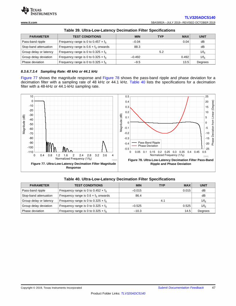
Normalized Frequency (1/fS)
Magn
itude
(dB
)
0 0.4 0.8 1.2 1.6 2 2.4 2.8 3.2 3.6 4-110
-100
-90
-80
-70
-60
-50
-40
-30
-20
-10
0
10
D003
Normalized Frequency (1/fS)
Magnitude (
dB
)
Phase D
evia
tion fro
m L
inear
(Degre
e)
0 0.05 0.1 0.15 0.2 0.25 0.3 0.35 0.4 0.45 0.5-0.5 -25
-0.4 -20
-0.3 -15
-0.2 -10
-0.1 -5
0 0
0.1 5
0.2 10
0.3 15
0.4 20
0.5 25
D003
Pass-Band RipplePhase Deviation
47
TLV320ADC5140www.ti.com SBAS892A –JULY 2019–REVISED OCTOBER 2019
Product Folder Links: TLV320ADC5140
Submit Documentation FeedbackCopyright © 2019, Texas Instruments Incorporated
Table 39. Ultra-Low-Latency Decimation Filter SpecificationsPARAMETER TEST CONDITIONS MIN TYP MAX UNIT
Pass-band ripple Frequency range is 0 to 0.457 × fS –0.04 0.04 dBStop-band attenuation Frequency range is 0.6 × fS onwards 88.3 dBGroup delay or latency Frequency range is 0 to 0.325 × fS 5.2 1/fSGroup delay deviation Frequency range is 0 to 0.325 × fS –0.492 0.492 1/fSPhase deviation Frequency range is 0 to 0.325 × fS –9.5 13.5 Degrees
8.3.6.7.3.4 Sampling Rate: 48 kHz or 44.1 kHz
Figure 77 shows the magnitude response and Figure 78 shows the pass-band ripple and phase deviation for adecimation filter with a sampling rate of 48 kHz or 44.1 kHz. Table 40 lists the specifications for a decimationfilter with a 48-kHz or 44.1-kHz sampling rate.
Figure 77. Ultra-Low-Latency Decimation Filter MagnitudeResponse
Figure 78. Ultra-Low-Latency Decimation Filter Pass-BandRipple and Phase Deviation
Table 40. Ultra-Low-Latency Decimation Filter SpecificationsPARAMETER TEST CONDITIONS MIN TYP MAX UNIT
Pass-band ripple Frequency range is 0 to 0.452 × fS –0.015 0.015 dBStop-band attenuation Frequency range is 0.6 × fS onwards 86.4 dBGroup delay or latency Frequency range is 0 to 0.325 × fS 4.1 1/fSGroup delay deviation Frequency range is 0 to 0.325 × fS –0.525 0.525 1/fSPhase deviation Frequency range is 0 to 0.325 × fS –10.3 14.5 Degrees
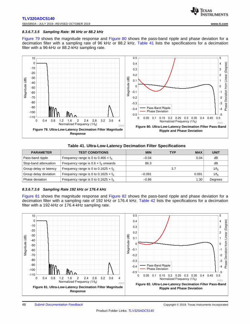
Normalized Frequency (1/fS)
Magn
itude
(dB
)
0 0.4 0.8 1.2 1.6 2 2.4 2.8 3.2 3.6 4-110
-100
-90
-80
-70
-60
-50
-40
-30
-20
-10
0
10
D003
Normalized Frequency (1/fS)
Magnitude (
dB
)
Phase D
evia
tion fro
m L
inear
(Degre
e)
0 0.05 0.1 0.15 0.2 0.25 0.3 0.35 0.4 0.45 0.5-0.5 -5
-0.4 -4
-0.3 -3
-0.2 -2
-0.1 -1
0 0
0.1 1
0.2 2
0.3 3
0.4 4
0.5 5
D003
Pass-Band RipplePhase Deviation
Normalized Frequency (1/fS)
Magn
itude
(dB
)
0 0.4 0.8 1.2 1.6 2 2.4 2.8 3.2 3.6 4-110
-100
-90
-80
-70
-60
-50
-40
-30
-20
-10
0
10
D003
Normalized Frequency (1/fS)
Magnitude (
dB
)
Phase D
evia
tion fro
m L
inear
(Degre
e)
0 0.05 0.1 0.15 0.2 0.25 0.3 0.35 0.4 0.45 0.5-0.5 -5
-0.4 -4
-0.3 -3
-0.2 -2
-0.1 -1
0 0
0.1 1
0.2 2
0.3 3
0.4 4
0.5 5
D003
Pass-Band RipplePhase Deviation
48
TLV320ADC5140SBAS892A –JULY 2019–REVISED OCTOBER 2019 www.ti.com
Product Folder Links: TLV320ADC5140
Submit Documentation Feedback Copyright © 2019, Texas Instruments Incorporated
8.3.6.7.3.5 Sampling Rate: 96 kHz or 88.2 kHz
Figure 79 shows the magnitude response and Figure 80 shows the pass-band ripple and phase deviation for adecimation filter with a sampling rate of 96 kHz or 88.2 kHz. Table 41 lists the specifications for a decimationfilter with a 96-kHz or 88.2-kHz sampling rate.
Figure 79. Ultra-Low-Latency Decimation Filter MagnitudeResponse
Figure 80. Ultra-Low-Latency Decimation Filter Pass-BandRipple and Phase Deviation
Table 41. Ultra-Low-Latency Decimation Filter SpecificationsPARAMETER TEST CONDITIONS MIN TYP MAX UNIT
Pass-band ripple Frequency range is 0 to 0.466 × fS –0.04 0.04 dBStop-band attenuation Frequency range is 0.6 × fS onwards 86.3 dBGroup delay or latency Frequency range is 0 to 0.1625 × fS 3.7 1/fSGroup delay deviation Frequency range is 0 to 0.1625 × fS –0.091 0.091 1/fSPhase deviation Frequency range is 0 to 0.1625 × fS –0.86 1.30 Degrees
8.3.6.7.3.6 Sampling Rate 192 kHz or 176.4 kHz
Figure 81 shows the magnitude response and Figure 82 shows the pass-band ripple and phase deviation for adecimation filter with a sampling rate of 192 kHz or 176.4 kHz. Table 42 lists the specifications for a decimationfilter with a 192-kHz or 176.4-kHz sampling rate.
Figure 81. Ultra-Low-Latency Decimation Filter MagnitudeResponse
Figure 82. Ultra-Low-Latency Decimation Filter Pass-BandRipple and Phase Deviation
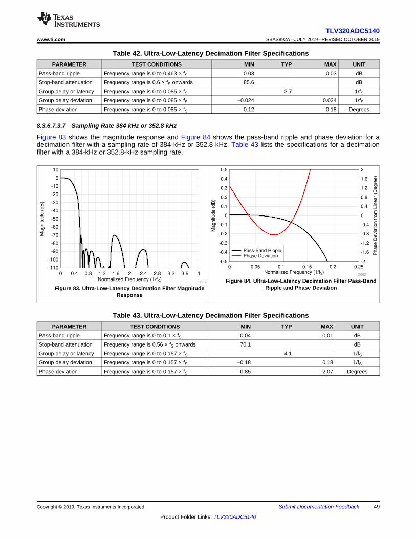
Normalized Frequency (1/fS)
Magn
itude
(dB
)
0 0.4 0.8 1.2 1.6 2 2.4 2.8 3.2 3.6 4-110
-100
-90
-80
-70
-60
-50
-40
-30
-20
-10
0
10
D002
Normalized Frequency (1/fS)
Magnitude (
dB
)
Phase D
evia
tion fro
m L
inear
(Degre
e)
0 0.05 0.1 0.15 0.2 0.25-0.5 -2
-0.4 -1.6
-0.3 -1.2
-0.2 -0.8
-0.1 -0.4
0 0
0.1 0.4
0.2 0.8
0.3 1.2
0.4 1.6
0.5 2
D002
Pass-Band RipplePhase Deviation
49
TLV320ADC5140www.ti.com SBAS892A –JULY 2019–REVISED OCTOBER 2019
Product Folder Links: TLV320ADC5140
Submit Documentation FeedbackCopyright © 2019, Texas Instruments Incorporated
Table 42. Ultra-Low-Latency Decimation Filter SpecificationsPARAMETER TEST CONDITIONS MIN TYP MAX UNIT
Pass-band ripple Frequency range is 0 to 0.463 × fS –0.03 0.03 dBStop-band attenuation Frequency range is 0.6 × fS onwards 85.6 dBGroup delay or latency Frequency range is 0 to 0.085 × fS 3.7 1/fSGroup delay deviation Frequency range is 0 to 0.085 × fS –0.024 0.024 1/fSPhase deviation Frequency range is 0 to 0.085 × fS –0.12 0.18 Degrees
8.3.6.7.3.7 Sampling Rate 384 kHz or 352.8 kHz
Figure 83 shows the magnitude response and Figure 84 shows the pass-band ripple and phase deviation for adecimation filter with a sampling rate of 384 kHz or 352.8 kHz. Table 43 lists the specifications for a decimationfilter with a 384-kHz or 352.8-kHz sampling rate.
Figure 83. Ultra-Low-Latency Decimation Filter MagnitudeResponse
Figure 84. Ultra-Low-Latency Decimation Filter Pass-BandRipple and Phase Deviation
Table 43. Ultra-Low-Latency Decimation Filter SpecificationsPARAMETER TEST CONDITIONS MIN TYP MAX UNIT
Pass-band ripple Frequency range is 0 to 0.1 × fS –0.04 0.01 dBStop-band attenuation Frequency range is 0.56 × fS onwards 70.1 dBGroup delay or latency Frequency range is 0 to 0.157 × fS 4.1 1/fSGroup delay deviation Frequency range is 0 to 0.157 × fS –0.18 0.18 1/fSPhase deviation Frequency range is 0 to 0.157 × fS –0.85 2.07 Degrees
50
TLV320ADC5140SBAS892A –JULY 2019–REVISED OCTOBER 2019 www.ti.com
Product Folder Links: TLV320ADC5140
Submit Documentation Feedback Copyright © 2019, Texas Instruments Incorporated
8.3.7 Dynamic Range Enhancer (DRE)The device integrates an ultra-low noise front-end PGA with 120-dB dynamic range performance with a low-noise, low-distortion, multibit delta-sigma (ΔΣ) ADC with a 108-dB dynamic range. The dynamic range enhancer(DRE) is a digitally assisted algorithm to boost the overall channel performance. The DRE monitors the incomingsignal amplitude and accordingly adjusts the internal PGA gain automatically. The DRE achieves a complete-channel dynamic range as high as 120 dB. At a system level, the DRE scheme enables far-field, high-fidelityrecording of audio signals in very quiet environments and low-distortion recording in loud environments.
This algorithm is implemented with very low latency and all signal chain blocks are designed to minimize anyaudible artifacts that may occur resulting from dynamic gain modulation. Additionally, the host can configure thetarget signal threshold level at which DRE is triggered by setting the appropriate value for the DRE_LVL[3:0],P0_R109[7:4] register bits. The DRE_LVL default level is set to –54 dB and TI recommends setting theDRE_LVL value lower than –30 dB to maximize the benefit of the DRE in real-world applications and to minimizeany audible artifacts. Table 44 lists the DRE_LVL configuration settings.
Table 44. DRE Trigger Threshold Level Programmable SettingsP0_R109_D[7:4] : DRE_LVL[3:0] DRE TRIGGER THRESHOLD LEVEL
0000 The DRE trigger threshold is the –12-dB input signal level0001 The DRE trigger threshold is the –18-dB input signal level0010 The DRE trigger threshold is the –24-dB input signal level
… …0111 (default) The DRE trigger threshold is the –54-dB input signal level
… …1001 The DRE trigger threshold is the –66-dB input signal level
1010 to 1111 Reserved (do not use these settings)
The DRE gain range can be dynamically modulated by using the DRE_MAXGAIN[3:0, P0_R109[3:0] registerbits. The DRE_MAXGAIN default value is set to 24 dB, and the DRE_MAXGAIN value is recommended to be setlower than 24 dB to maximize the benefit of the DRE in real-world applications and to minimize any audibleartifacts. Table 45 lists the DRE_MAXGAIN configuration settings.
Table 45. DRE Maximum Gain Programmable SettingsP0_R109_D[3:0] : DRE_MAXGAIN[3:0] DRE MAXIMUM GAIN ALLOWED
0000 The DRE maximum gain allowed is 2 dB0001 The DRE maximum gain allowed is 4 dB0010 The DRE maximum gain allowed is 6 dB
… …1011 (default) The DRE maximum gain allowed is 24 dB
… …1110 The DRE maximum gain allowed is 30 dB1111 Reserved (do not use this setting)
The DRE scheme is only supported for analog microphone recording channels with an AC-coupled input for bestdynamic range performance. The DRE scheme can be independently enabled or disabled for each channel usingthe CH1_DREEN (P0_R60_D0), CH2_DREEN (P0_R65_D0), CH3_DREEN (P0_R70_D0), and CH4_DREEN(P0_R75_D0) register bits. For a DC-coupled input, the DRE scheme can be used with limited DRE_MAXGAINdepending on the DC differential input common-mode offset.
Enabling the DRE for processing increases the power consumption of the device because of increased signalprocessing. Therefore, disable the DRE for low-power critical applications. Furthermore, the DRE is notsupported for output sample rates greater than 192 kHz.
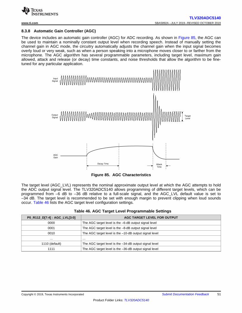
Target
Level
Attack
Time
Decay Time
Input
Signal
Output
Signal
AGC
Gain
51
TLV320ADC5140www.ti.com SBAS892A –JULY 2019–REVISED OCTOBER 2019
Product Folder Links: TLV320ADC5140
Submit Documentation FeedbackCopyright © 2019, Texas Instruments Incorporated
8.3.8 Automatic Gain Controller (AGC)The device includes an automatic gain controller (AGC) for ADC recording. As shown in Figure 85, the AGC canbe used to maintain a nominally constant output level when recording speech. Instead of manually setting thechannel gain in AGC mode, the circuitry automatically adjusts the channel gain when the input signal becomesoverly loud or very weak, such as when a person speaking into a microphone moves closer to or farther from themicrophone. The AGC algorithm has several programmable parameters, including target level, maximum gainallowed, attack and release (or decay) time constants, and noise thresholds that allow the algorithm to be fine-tuned for any particular application.
Figure 85. AGC Characteristics
The target level (AGC_LVL) represents the nominal approximate output level at which the AGC attempts to holdthe ADC output signal level. The TLV320ADC5140 allows programming of different target levels, which can beprogrammed from –6 dB to –36 dB relative to a full-scale signal, and the AGC_LVL default value is set to–34 dB. The target level is recommended to be set with enough margin to prevent clipping when loud soundsoccur. Table 46 lists the AGC target level configuration settings.
Table 46. AGC Target Level Programmable SettingsP0_R112_D[7:4] : AGC_LVL[3:0] AGC TARGET LEVEL FOR OUTPUT
0000 The AGC target level is the –6-dB output signal level0001 The AGC target level is the –8-dB output signal level0010 The AGC target level is the –10-dB output signal level
… …1110 (default) The AGC target level is the –34-dB output signal level
1111 The AGC target level is the –36-dB output signal level
52
TLV320ADC5140SBAS892A –JULY 2019–REVISED OCTOBER 2019 www.ti.com
Product Folder Links: TLV320ADC5140
Submit Documentation Feedback Copyright © 2019, Texas Instruments Incorporated
The maximum gain allowed (AGC_MAXGAIN) gives flexibility to the designer to restrict the maximum gainapplied by the AGC. This feature limits the channel gain in situations where environmental noise is greater thanthe programmed noise threshold. The AGC_MAXGAIN can be programmed from 3 dB to 42 dB with steps of 3dB and the default value is set to 24 dB. Table 47 lists the AGC_MAXGAIN configuration settings.
Table 47. AGC Maximum Gain Programmable SettingsP0_R112_D[3:0] : AGC_MAXGAIN[3:0] AGC MAXIMUM GAIN ALLOWED
0000 The AGC maximum gain allowed is 3 dB0001 The AGC maximum gain allowed is 6 dB0010 The AGC maximum gain allowed is 9 dB
… …0111 (default) The AGC maximum gain allowed is 24 dB
… …1110 The AGC maximum gain allowed is 39 dB1111 The AGC maximum gain allowed is 42 dB
For further details on the AGC various configurable parameter and application use, see the Using the AutomaticGain Controller (AGC) in TLV320ADCx140 application report.
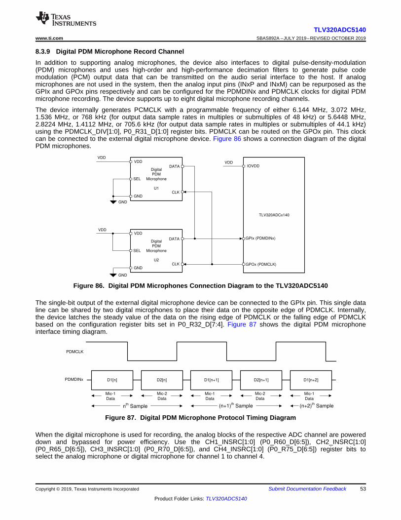
D1[n] D2[n] D1[n+1] D2[n+1] D1[n+2]
PDMCLK
PDMDINx
Mic-1
Data
Mic-2
Data
(n+1)th Sample n
th Sample (n+2)
th Sample
Mic-1
Data
Mic-2
DataMic-1
Data
VDD
Digital
PDM
Microphone
U1
DATA
CLKGND
VDD
SEL
Digital
PDM
Microphone
U2
DATA
CLKGND
VDD
SEL
VDD
TLV320ADCx140
IOVDD
VDD
GPIx (PDMDINx)
GPOx (PDMCLK)
GND
GND
53
TLV320ADC5140www.ti.com SBAS892A –JULY 2019–REVISED OCTOBER 2019
Product Folder Links: TLV320ADC5140
Submit Documentation FeedbackCopyright © 2019, Texas Instruments Incorporated
8.3.9 Digital PDM Microphone Record ChannelIn addition to supporting analog microphones, the device also interfaces to digital pulse-density-modulation(PDM) microphones and uses high-order and high-performance decimation filters to generate pulse codemodulation (PCM) output data that can be transmitted on the audio serial interface to the host. If analogmicrophones are not used in the system, then the analog input pins (INxP and INxM) can be repurposed as theGPIx and GPOx pins respectively and can be configured for the PDMDINx and PDMCLK clocks for digital PDMmicrophone recording. The device supports up to eight digital microphone recording channels.
The device internally generates PCMCLK with a programmable frequency of either 6.144 MHz, 3.072 MHz,1.536 MHz, or 768 kHz (for output data sample rates in multiples or submultiples of 48 kHz) or 5.6448 MHz,2.8224 MHz, 1.4112 MHz, or 705.6 kHz (for output data sample rates in multiples or submultiples of 44.1 kHz)using the PDMCLK_DIV[1:0], P0_R31_D[1:0] register bits. PDMCLK can be routed on the GPOx pin. This clockcan be connected to the external digital microphone device. Figure 86 shows a connection diagram of the digitalPDM microphones.
Figure 86. Digital PDM Microphones Connection Diagram to the TLV320ADC5140
The single-bit output of the external digital microphone device can be connected to the GPIx pin. This single dataline can be shared by two digital microphones to place their data on the opposite edge of PDMCLK. Internally,the device latches the steady value of the data on the rising edge of PDMCLK or the falling edge of PDMCLKbased on the configuration register bits set in P0_R32_D[7:4]. Figure 87 shows the digital PDM microphoneinterface timing diagram.
Figure 87. Digital PDM Microphone Protocol Timing Diagram
When the digital microphone is used for recording, the analog blocks of the respective ADC channel are powereddown and bypassed for power efficiency. Use the CH1_INSRC[1:0] (P0_R60_D[6:5]), CH2_INSRC[1:0](P0_R65_D[6:5]), CH3_INSRC[1:0] (P0_R70_D[6:5]), and CH4_INSRC[1:0] (P0_R75_D[6:5]) register bits toselect the analog microphone or digital microphone for channel 1 to channel 4.
54
TLV320ADC5140SBAS892A –JULY 2019–REVISED OCTOBER 2019 www.ti.com
Product Folder Links: TLV320ADC5140
Submit Documentation Feedback Copyright © 2019, Texas Instruments Incorporated
(1) Only the GPIO1 pin is with reference to the IOVDD supply, the other GPOx and GPIx pins are with reference to the AVDD supply andtheir primary pin functions are for the PDMCLK or PDMDIN function.
(2) S means the feature mentioned in this row is supported for the respective GPIO1, GPOx, or GPIx pin mentioned in this column.(3) NS means the feature mentioned in this row is not supported for the respective GPIO1, GPOx, or GPIx pin mentioned in this column.(4) For the high-speed ASI output, GPIO1 must be used instead of GPOx for the secondary ASI output. GPOx can be used only if the bus
speed requirement is less than 6.144 MHz.
8.3.10 Interrupts, Status, and Digital I/O Pin MultiplexingCertain events in the device may require host processor intervention and can be used to trigger interrupts to thehost processor. One such event is an audio serial interface (ASI) bus error. The device powers down the recordchannels if any faults are detected with the ASI bus error clocks, such as:• Invalid FSYNC frequency• Invalid SBCLK to FSYNC ratio• Long pauses of the SBCLK or FSYNC clocks
When an ASI bus clock error is detected, the device shuts down the record channel as quickly as possible. Afterall ASI bus clock errors are resolved, the device volume ramps back to its previous state to recover the recordchannel. During an ASI bus clock error, the internal interrupt request (IRQ) interrupt signal asserts low if theclock error interrupt mask register bit INT_MASK0[7], P0_R51_D7 is set low. The clock fault is also available forreadback in the latched fault status register bit INT_LTCH0, P0_R54, which is a read-only register. Reading thelatched fault status register, INT_LTCH0, clears all latched fault status. The device can be additionally configuredto route the internal IRQ interrupt signal on the GPIO1 or GPOx pins and also can be configured as open-drainoutputs so that these pins can be wire-ANDed to the open-drain interrupt outputs of other devices.
The IRQ interrupt signal can either be configured as active low or active high polarity by setting the INT_POL,P0_R50_D7 register bit. This signal can also be configured as a single pulse or a series of pulses byprogramming the INT_EVENT[1:0], P0_R50_D[6:5] register bits. If the interrupts are configured as a series ofpulses, the events trigger the start of pulses that stop when the latched fault status register is read to determinethe cause of the interrupt.
The device also supports read-only live-status registers to determine if the channels are powered up or down andif the device is in sleep mode or not. These status registers are located in P0_R118, DEV_STS0 and P0_R119,DEV_STS1.
The device has a multifunctional GPIO1 pin that can be configured for a desired specific function. Additionally, ifthe channel is not used for analog input recording, then the analog input pins for that channel (INxP and INxM)can be repurposed as multifunction pins (GPIx and GPOx) by configuring the CHx_INSRC[1:0] register bitslocated in the CHx_CFG0 register. The maximum number of GPO pins supported by the device is four and themaximum number of GPI pins are four. Table 48 shows all possible allocations of these multifunctional pins forthe various features.
Table 48. Multifunction Pin AssignmentsROW Pin Function (1) GPIO1 GPO1 GPO2 GPO3 GPO4 GPI1 GPI2 GPI3 GPI4
— — GPIO1_CFG GPO1_CFG GPO2_CFG GPO3_CFG GPO4_CFG GPI1_CFG GPI2_CFG GPI3_CFG GPI4_CFG
— — P0_R33[7:4] P0_R34[7:4] P0_R35[7:4] P0_R36[7:4] P0_R37[7:4] P0_R43[6:4] P0_R43[2:0] P0_R44[6:4] P0_R44[2:0]
A Pin disabled S (2) S (default) S (default) S (default) S (default) S (default) S (default) S (default) S (default)
B General-purpose output(GPO) S S S S S NS (3) NS NS NS
C Interrupt output (IRQ) S (default) S S S S NS NS NS NS
D Secondary ASI output(SDOUT2)(4) S S S S S NS NS NS NS
E PDM clock output (PDMCLK) S S S S S NS NS NS NS
F MiCBIAS on/off input(BIASEN) S NS NS NS NS NS NS NS NS
G General-purpose input (GPI) S NS NS NS NS S S S S
H Master clock input (MCLK) S NS NS NS NS S S S S
I ASI daisy-chain input (SDIN) S NS NS NS NS S S S S
J PDM data input 1 (PDMDIN1) S NS NS NS NS S S S S
K PDM data input 2 (PDMDIN2) S NS NS NS NS S S S S
L PDM data input 3 (PDMDIN3) S NS NS NS NS S S S S
M PDM data input 4 (PDMDIN4) S NS NS NS NS S S S S
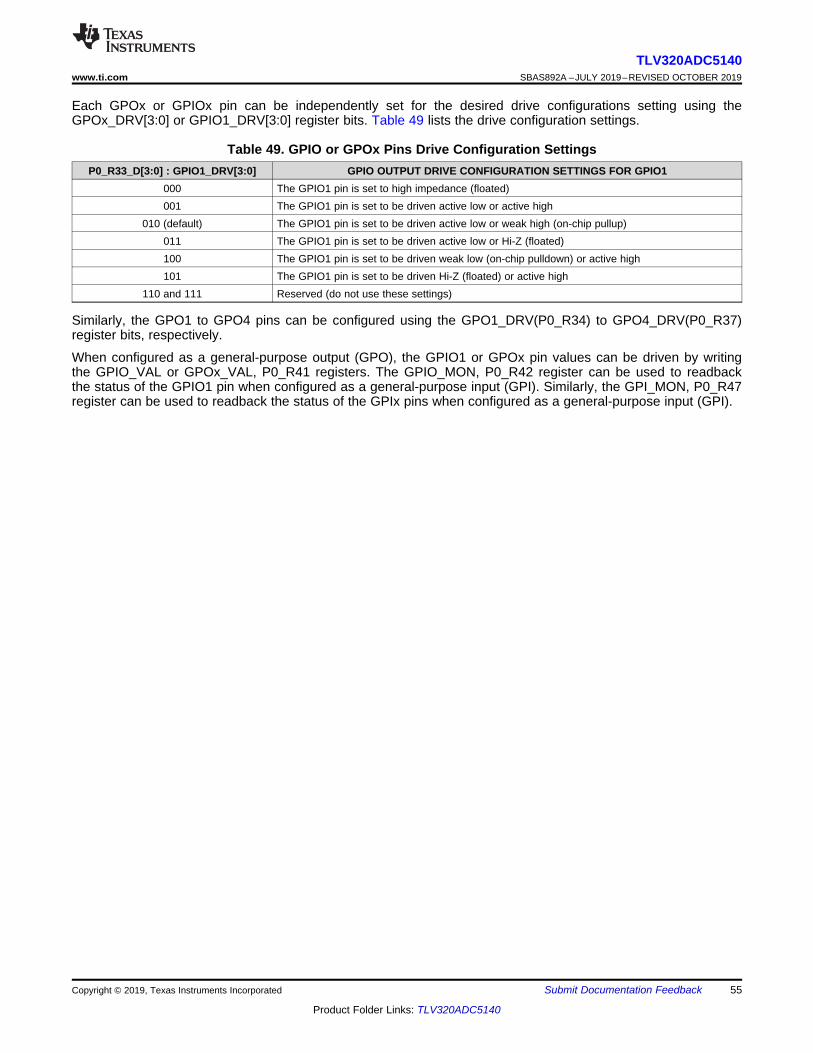
55
TLV320ADC5140www.ti.com SBAS892A –JULY 2019–REVISED OCTOBER 2019
Product Folder Links: TLV320ADC5140
Submit Documentation FeedbackCopyright © 2019, Texas Instruments Incorporated
Each GPOx or GPIOx pin can be independently set for the desired drive configurations setting using theGPOx_DRV[3:0] or GPIO1_DRV[3:0] register bits. Table 49 lists the drive configuration settings.
Table 49. GPIO or GPOx Pins Drive Configuration SettingsP0_R33_D[3:0] : GPIO1_DRV[3:0] GPIO OUTPUT DRIVE CONFIGURATION SETTINGS FOR GPIO1
000 The GPIO1 pin is set to high impedance (floated)001 The GPIO1 pin is set to be driven active low or active high
010 (default) The GPIO1 pin is set to be driven active low or weak high (on-chip pullup)011 The GPIO1 pin is set to be driven active low or Hi-Z (floated)100 The GPIO1 pin is set to be driven weak low (on-chip pulldown) or active high101 The GPIO1 pin is set to be driven Hi-Z (floated) or active high
110 and 111 Reserved (do not use these settings)
Similarly, the GPO1 to GPO4 pins can be configured using the GPO1_DRV(P0_R34) to GPO4_DRV(P0_R37)register bits, respectively.
When configured as a general-purpose output (GPO), the GPIO1 or GPOx pin values can be driven by writingthe GPIO_VAL or GPOx_VAL, P0_R41 registers. The GPIO_MON, P0_R42 register can be used to readbackthe status of the GPIO1 pin when configured as a general-purpose input (GPI). Similarly, the GPI_MON, P0_R47register can be used to readback the status of the GPIx pins when configured as a general-purpose input (GPI).
56
TLV320ADC5140SBAS892A –JULY 2019–REVISED OCTOBER 2019 www.ti.com
Product Folder Links: TLV320ADC5140
Submit Documentation Feedback Copyright © 2019, Texas Instruments Incorporated
8.4 Device Functional Modes
8.4.1 Hardware ShutdownThe device enters hardware shutdown mode when the SHDNZ pin is asserted low or the AVDD supply voltage isnot applied to the device. In hardware shutdown mode, the device consumes the minimum quiescent currentfrom the AVDD supply. All configuration registers and programmable coefficients lose their value in this mode,and I2C or SPI communication to the device is not supported.
If the SHDNZ pin is asserted low when the device is in active mode, the device ramps down volume on therecord data, powers down the analog and digital blocks, and puts the device into hardware shutdown mode in 25ms (typical). The device can also be immediately put into hardware shutdown mode from active mode if theSHDNZ_CFG[1:0], P0_R5_D[3:2], register bits are set to 2'b00. After the SHDNZ pin is asserted low, and afterthe device enters hardware shutdown mode, keep the SHDNZ pin low for at least 1 ms before releasing SHDNZfor further device operation.
Assert the SHDNZ pin high only when the IOVDD supply settles to a steady voltage level. When the SHDNZ pingoes high, the device sets all configuration registers and programmable coefficients to their default values, andthen enters sleep mode.
8.4.2 Sleep Mode or Software ShutdownIn sleep mode or software shutdown mode, the device consumes very low quiescent current from the AVDDsupply and, at the same time, allows the I2C or SPI communication to wake the device for active operation.
The device can also enter sleep mode when the host device sets the SLEEP_ENZ, P0_R2_D0 bit to 1'b0. If theSLEEP_ENZ bit is asserted low when the device is in active mode, the device ramps down the volume on therecord data, powers down the analog and digital blocks, and enters sleep mode. However, the device stillcontinues to retain the last programmed value of the device configuration registers and programmablecoefficients.
In sleep mode, do not perform any I2C or SPI transactions, except for exiting sleep mode in order to enter activemode. After entering sleep mode, wait at least 10 ms before starting I2C or SPI transactions to exit sleep mode.
While exiting sleep mode, the host device must configure the TLV320ADC5140 to use either an external 1.8-VAREG supply (default setting) or an on-chip-regulator-generated AREG supply. To configure the AREG supply,write to AREG_SELECT, bit D7 in the same P0_R2 register.
8.4.3 Active ModeIf the host device exits sleep mode by setting the SLEEP_ENZ bit to 1'b1, the device enters active mode. Inactive mode, I2C or SPI transactions can be done to configure and power-up the device for active operation.After entering active mode, wait at least 1 ms before starting any I2C or SPI transactions in order to allow thedevice to complete the internal wake-up sequence.
After configuring all other registers for the target application and system settings, configure the input and outputchannel enable registers, P0_R115 (IN_CH_EN) and P0_R116 (ASI_OUT_CH_EN), respectively. Lastly,configure the device power-up register, P0_R117 (PWR_CFG). All the programmable coefficient values must bewritten before powering up the respective channel.
In active mode, the power-up and power-down status of various blocks is monitored by reading the read-onlydevice status bits located in the P0_R117 (DEV_STS0) and P0_R118 (DEV_STS1) registers.
8.4.4 Software ResetA software reset can be done any time by asserting the SW_RESET bit, P0_R1_D0, which is a self-clearing bit.This software reset immediately shuts down the device, and restores all device configuration registers andprogrammable coefficients to their default values.
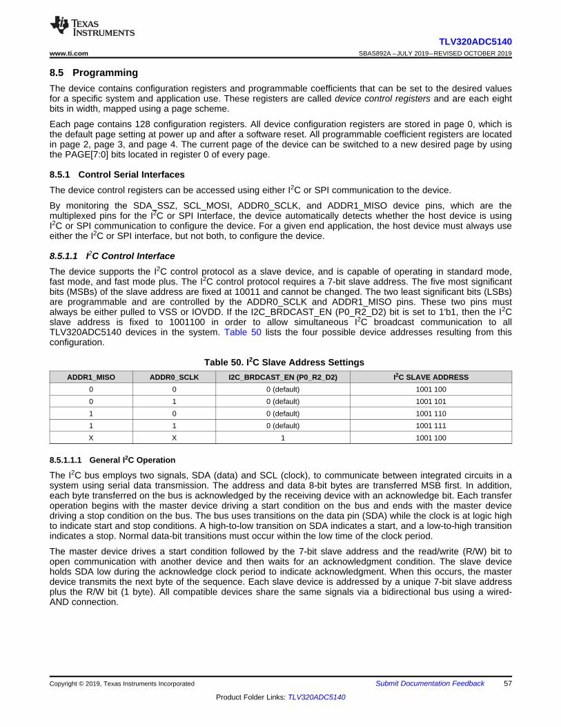
57
TLV320ADC5140www.ti.com SBAS892A –JULY 2019–REVISED OCTOBER 2019
Product Folder Links: TLV320ADC5140
Submit Documentation FeedbackCopyright © 2019, Texas Instruments Incorporated
8.5 ProgrammingThe device contains configuration registers and programmable coefficients that can be set to the desired valuesfor a specific system and application use. These registers are called device control registers and are each eightbits in width, mapped using a page scheme.
Each page contains 128 configuration registers. All device configuration registers are stored in page 0, which isthe default page setting at power up and after a software reset. All programmable coefficient registers are locatedin page 2, page 3, and page 4. The current page of the device can be switched to a new desired page by usingthe PAGE[7:0] bits located in register 0 of every page.
8.5.1 Control Serial InterfacesThe device control registers can be accessed using either I2C or SPI communication to the device.
By monitoring the SDA_SSZ, SCL_MOSI, ADDR0_SCLK, and ADDR1_MISO device pins, which are themultiplexed pins for the I2C or SPI Interface, the device automatically detects whether the host device is usingI2C or SPI communication to configure the device. For a given end application, the host device must always useeither the I2C or SPI interface, but not both, to configure the device.
8.5.1.1 I2C Control InterfaceThe device supports the I2C control protocol as a slave device, and is capable of operating in standard mode,fast mode, and fast mode plus. The I2C control protocol requires a 7-bit slave address. The five most significantbits (MSBs) of the slave address are fixed at 10011 and cannot be changed. The two least significant bits (LSBs)are programmable and are controlled by the ADDR0_SCLK and ADDR1_MISO pins. These two pins mustalways be either pulled to VSS or IOVDD. If the I2C_BRDCAST_EN (P0_R2_D2) bit is set to 1'b1, then the I2Cslave address is fixed to 1001100 in order to allow simultaneous I2C broadcast communication to allTLV320ADC5140 devices in the system. Table 50 lists the four possible device addresses resulting from thisconfiguration.
Table 50. I2C Slave Address SettingsADDR1_MISO ADDR0_SCLK I2C_BRDCAST_EN (P0_R2_D2) I2C SLAVE ADDRESS
0 0 0 (default) 1001 1000 1 0 (default) 1001 1011 0 0 (default) 1001 1101 1 0 (default) 1001 111X X 1 1001 100
8.5.1.1.1 General I2C Operation
The I2C bus employs two signals, SDA (data) and SCL (clock), to communicate between integrated circuits in asystem using serial data transmission. The address and data 8-bit bytes are transferred MSB first. In addition,each byte transferred on the bus is acknowledged by the receiving device with an acknowledge bit. Each transferoperation begins with the master device driving a start condition on the bus and ends with the master devicedriving a stop condition on the bus. The bus uses transitions on the data pin (SDA) while the clock is at logic highto indicate start and stop conditions. A high-to-low transition on SDA indicates a start, and a low-to-high transitionindicates a stop. Normal data-bit transitions must occur within the low time of the clock period.
The master device drives a start condition followed by the 7-bit slave address and the read/write (R/W) bit toopen communication with another device and then waits for an acknowledgment condition. The slave deviceholds SDA low during the acknowledge clock period to indicate acknowledgment. When this occurs, the masterdevice transmits the next byte of the sequence. Each slave device is addressed by a unique 7-bit slave addressplus the R/W bit (1 byte). All compatible devices share the same signals via a bidirectional bus using a wired-AND connection.
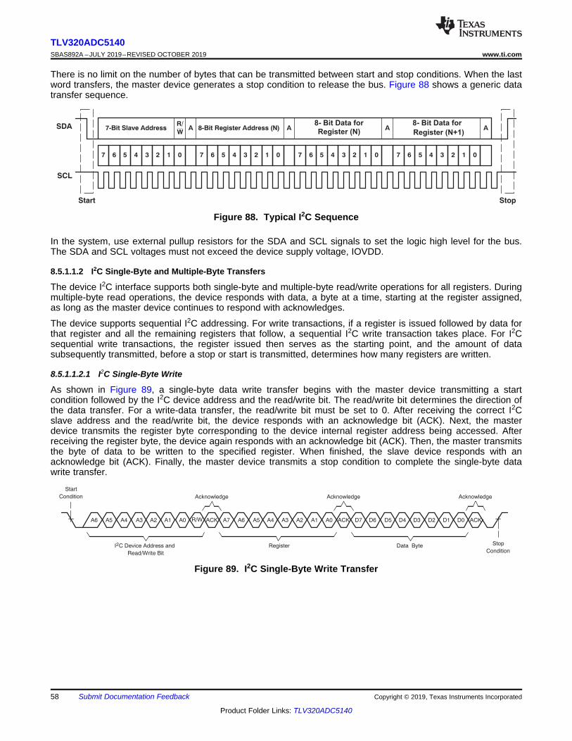
A6 A5 A4 A3 A2 A1 A0 R/W ACK A7 A6 A5 A4 A3 A2 A1 A0 ACK D7 D6 D5 D4 D3 D2 D1 D0 ACK
Start
Condition
Stop
Condition
Acknowledge Acknowledge Acknowledge
I2C Device Address and
Read/Write Bit
Register Data Byte
Register (N)8- Bit Data for 8- Bit Data for
Register (N+1)
58
TLV320ADC5140SBAS892A –JULY 2019–REVISED OCTOBER 2019 www.ti.com
Product Folder Links: TLV320ADC5140
Submit Documentation Feedback Copyright © 2019, Texas Instruments Incorporated
There is no limit on the number of bytes that can be transmitted between start and stop conditions. When the lastword transfers, the master device generates a stop condition to release the bus. Figure 88 shows a generic datatransfer sequence.
Figure 88. Typical I2C Sequence
In the system, use external pullup resistors for the SDA and SCL signals to set the logic high level for the bus.The SDA and SCL voltages must not exceed the device supply voltage, IOVDD.
8.5.1.1.2 I2C Single-Byte and Multiple-Byte Transfers
The device I2C interface supports both single-byte and multiple-byte read/write operations for all registers. Duringmultiple-byte read operations, the device responds with data, a byte at a time, starting at the register assigned,as long as the master device continues to respond with acknowledges.
The device supports sequential I2C addressing. For write transactions, if a register is issued followed by data forthat register and all the remaining registers that follow, a sequential I2C write transaction takes place. For I2Csequential write transactions, the register issued then serves as the starting point, and the amount of datasubsequently transmitted, before a stop or start is transmitted, determines how many registers are written.
8.5.1.1.2.1 I2C Single-Byte Write
As shown in Figure 89, a single-byte data write transfer begins with the master device transmitting a startcondition followed by the I2C device address and the read/write bit. The read/write bit determines the direction ofthe data transfer. For a write-data transfer, the read/write bit must be set to 0. After receiving the correct I2Cslave address and the read/write bit, the device responds with an acknowledge bit (ACK). Next, the masterdevice transmits the register byte corresponding to the device internal register address being accessed. Afterreceiving the register byte, the device again responds with an acknowledge bit (ACK). Then, the master transmitsthe byte of data to be written to the specified register. When finished, the slave device responds with anacknowledge bit (ACK). Finally, the master device transmits a stop condition to complete the single-byte datawrite transfer.
Figure 89. I2C Single-Byte Write Transfer
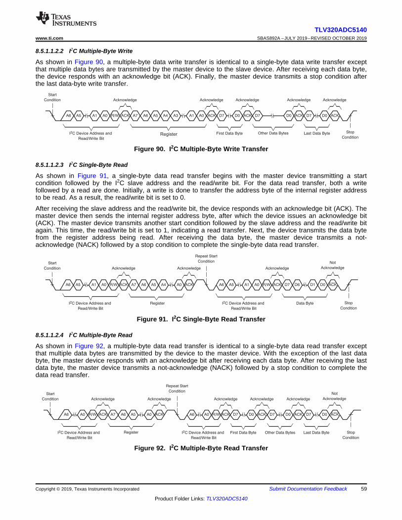
A6 A0 ACK
Acknowledge
I2C Device Address and
Read/Write Bit
R/WA6 A0 R/W ACK A0 ACK D7 D0 ACK
Start
Condition
Stop
Condition
Acknowledge Acknowledge Acknowledge
Last Data Byte
ACK
First Data Byte
Repeat Start
ConditionNot
Acknowledge
I2C Device Address and
Read/Write Bit
Register Other Data Bytes
A7 A6 A5 D7 D0 ACK
Acknowledge
D7 D0
A6 A5 A0 R/W ACK A7 A6 A5 A4 A0 ACK A6 A5 A0 ACK
Start
Condition
Stop
Condition
Acknowledge Acknowledge Acknowledge
I2C Device Address and
Read/Write Bit
Register Data Byte
D7 D6 D1 D0 ACK
I2C Device Address and
Read/Write Bit
Not
Acknowledge
R/WA1 A1
Repeat Start
Condition
Register
59
TLV320ADC5140www.ti.com SBAS892A –JULY 2019–REVISED OCTOBER 2019
Product Folder Links: TLV320ADC5140
Submit Documentation FeedbackCopyright © 2019, Texas Instruments Incorporated
8.5.1.1.2.2 I2C Multiple-Byte Write
As shown in Figure 90, a multiple-byte data write transfer is identical to a single-byte data write transfer exceptthat multiple data bytes are transmitted by the master device to the slave device. After receiving each data byte,the device responds with an acknowledge bit (ACK). Finally, the master device transmits a stop condition afterthe last data-byte write transfer.
Figure 90. I2C Multiple-Byte Write Transfer
8.5.1.1.2.3 I2C Single-Byte Read
As shown in Figure 91, a single-byte data read transfer begins with the master device transmitting a startcondition followed by the I2C slave address and the read/write bit. For the data read transfer, both a writefollowed by a read are done. Initially, a write is done to transfer the address byte of the internal register addressto be read. As a result, the read/write bit is set to 0.
After receiving the slave address and the read/write bit, the device responds with an acknowledge bit (ACK). Themaster device then sends the internal register address byte, after which the device issues an acknowledge bit(ACK). The master device transmits another start condition followed by the slave address and the read/write bitagain. This time, the read/write bit is set to 1, indicating a read transfer. Next, the device transmits the data bytefrom the register address being read. After receiving the data byte, the master device transmits a not-acknowledge (NACK) followed by a stop condition to complete the single-byte data read transfer.
Figure 91. I2C Single-Byte Read Transfer
8.5.1.1.2.4 I2C Multiple-Byte Read
As shown in Figure 92, a multiple-byte data read transfer is identical to a single-byte data read transfer exceptthat multiple data bytes are transmitted by the device to the master device. With the exception of the last databyte, the master device responds with an acknowledge bit after receiving each data byte. After receiving the lastdata byte, the master device transmits a not-acknowledge (NACK) followed by a stop condition to complete thedata read transfer.
Figure 92. I2C Multiple-Byte Read Transfer
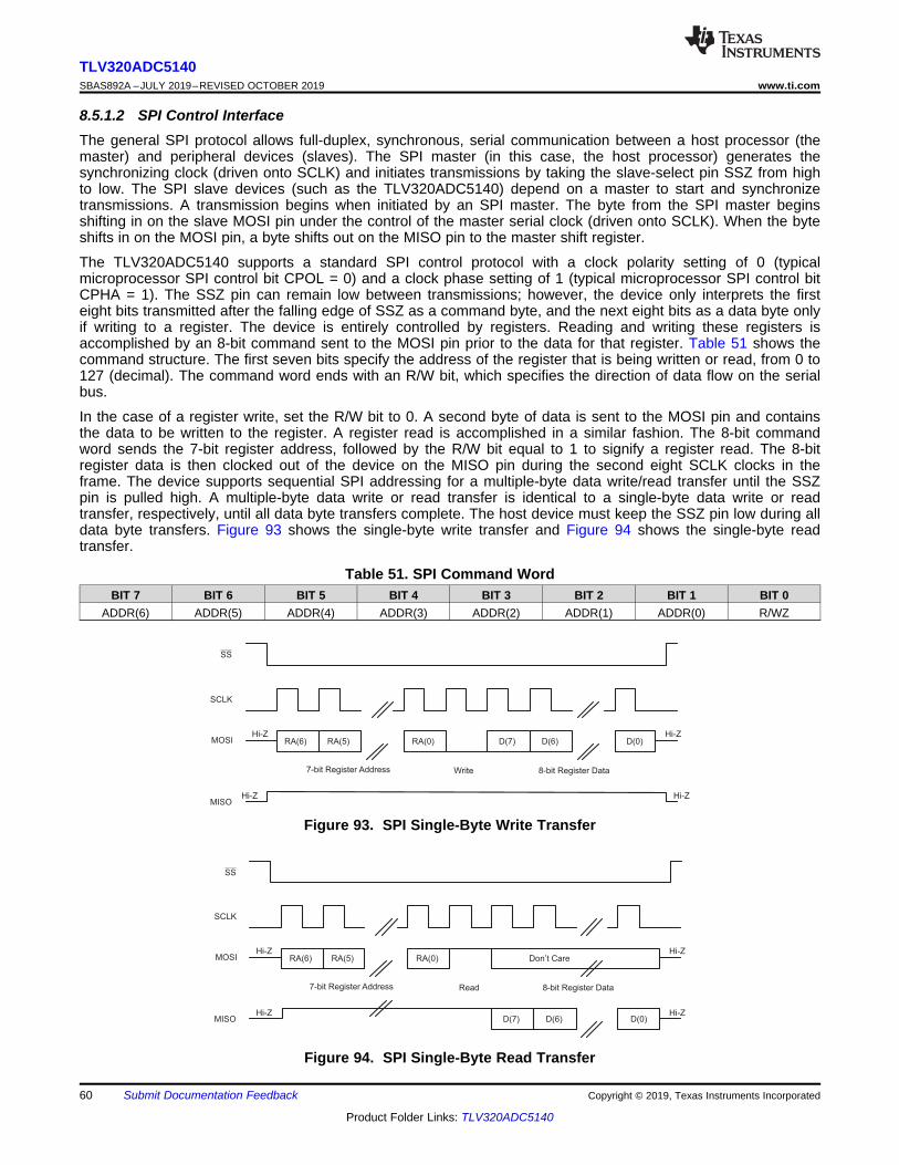
RA(6) RA(5) RA(0) Don’t Care
7-bit Register Address Read 8-bit Register Data
SS
SCLK
MOSI
MISO
Hi-Z Hi-Z
D(7) D(6) D(0)Hi-Z Hi-Z
RA(6) RA(5) RA(0) D(7) D(6) D(0)
7-bit Register Address Write 8-bit Register Data
SS
SCLK
MOSI
MISO
Hi-Z Hi-Z
Hi-Z Hi-Z
60
TLV320ADC5140SBAS892A –JULY 2019–REVISED OCTOBER 2019 www.ti.com
Product Folder Links: TLV320ADC5140
Submit Documentation Feedback Copyright © 2019, Texas Instruments Incorporated
8.5.1.2 SPI Control InterfaceThe general SPI protocol allows full-duplex, synchronous, serial communication between a host processor (themaster) and peripheral devices (slaves). The SPI master (in this case, the host processor) generates thesynchronizing clock (driven onto SCLK) and initiates transmissions by taking the slave-select pin SSZ from highto low. The SPI slave devices (such as the TLV320ADC5140) depend on a master to start and synchronizetransmissions. A transmission begins when initiated by an SPI master. The byte from the SPI master beginsshifting in on the slave MOSI pin under the control of the master serial clock (driven onto SCLK). When the byteshifts in on the MOSI pin, a byte shifts out on the MISO pin to the master shift register.
The TLV320ADC5140 supports a standard SPI control protocol with a clock polarity setting of 0 (typicalmicroprocessor SPI control bit CPOL = 0) and a clock phase setting of 1 (typical microprocessor SPI control bitCPHA = 1). The SSZ pin can remain low between transmissions; however, the device only interprets the firsteight bits transmitted after the falling edge of SSZ as a command byte, and the next eight bits as a data byte onlyif writing to a register. The device is entirely controlled by registers. Reading and writing these registers isaccomplished by an 8-bit command sent to the MOSI pin prior to the data for that register. Table 51 shows thecommand structure. The first seven bits specify the address of the register that is being written or read, from 0 to127 (decimal). The command word ends with an R/W bit, which specifies the direction of data flow on the serialbus.
In the case of a register write, set the R/W bit to 0. A second byte of data is sent to the MOSI pin and containsthe data to be written to the register. A register read is accomplished in a similar fashion. The 8-bit commandword sends the 7-bit register address, followed by the R/W bit equal to 1 to signify a register read. The 8-bitregister data is then clocked out of the device on the MISO pin during the second eight SCLK clocks in theframe. The device supports sequential SPI addressing for a multiple-byte data write/read transfer until the SSZpin is pulled high. A multiple-byte data write or read transfer is identical to a single-byte data write or readtransfer, respectively, until all data byte transfers complete. The host device must keep the SSZ pin low during alldata byte transfers. Figure 93 shows the single-byte write transfer and Figure 94 shows the single-byte readtransfer.
Table 51. SPI Command WordBIT 7 BIT 6 BIT 5 BIT 4 BIT 3 BIT 2 BIT 1 BIT 0
ADDR(6) ADDR(5) ADDR(4) ADDR(3) ADDR(2) ADDR(1) ADDR(0) R/WZ
Figure 93. SPI Single-Byte Write Transfer
Figure 94. SPI Single-Byte Read Transfer
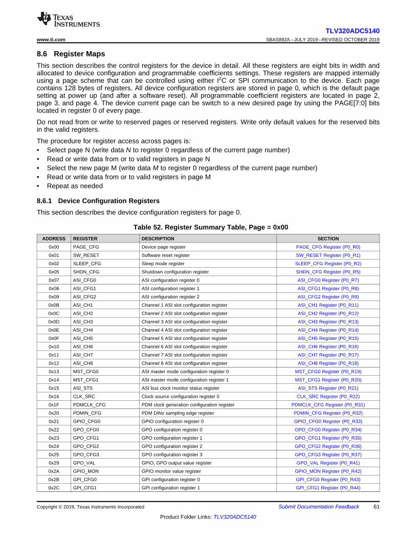
61
TLV320ADC5140www.ti.com SBAS892A –JULY 2019–REVISED OCTOBER 2019
Product Folder Links: TLV320ADC5140
Submit Documentation FeedbackCopyright © 2019, Texas Instruments Incorporated
8.6 Register MapsThis section describes the control registers for the device in detail. All these registers are eight bits in width andallocated to device configuration and programmable coefficients settings. These registers are mapped internallyusing a page scheme that can be controlled using either I2C or SPI communication to the device. Each pagecontains 128 bytes of registers. All device configuration registers are stored in page 0, which is the default pagesetting at power up (and after a software reset). All programmable coefficient registers are located in page 2,page 3, and page 4. The device current page can be switch to a new desired page by using the PAGE[7:0] bitslocated in register 0 of every page.
Do not read from or write to reserved pages or reserved registers. Write only default values for the reserved bitsin the valid registers.
The procedure for register access across pages is:• Select page N (write data N to register 0 regardless of the current page number)• Read or write data from or to valid registers in page N• Select the new page M (write data M to register 0 regardless of the current page number)• Read or write data from or to valid registers in page M• Repeat as needed
8.6.1 Device Configuration RegistersThis section describes the device configuration registers for page 0.
Table 52. Register Summary Table, Page = 0x00ADDRESS REGISTER DESCRIPTION SECTION
0x00 PAGE_CFG Device page register PAGE_CFG Register (P0_R0)
0x01 SW_RESET Software reset register SW_RESET Register (P0_R1)
0x02 SLEEP_CFG Sleep mode register SLEEP_CFG Register (P0_R2)
0x05 SHDN_CFG Shutdown configuration register SHDN_CFG Register (P0_R5)
0x07 ASI_CFG0 ASI configuration register 0 ASI_CFG0 Register (P0_R7)
0x08 ASI_CFG1 ASI configuration register 1 ASI_CFG1 Register (P0_R8)
0x09 ASI_CFG2 ASI configuration register 2 ASI_CFG2 Register (P0_R9)
0x0B ASI_CH1 Channel 1 ASI slot configuration register ASI_CH1 Register (P0_R11)
0x0C ASI_CH2 Channel 2 ASI slot configuration register ASI_CH2 Register (P0_R12)
0x0D ASI_CH3 Channel 3 ASI slot configuration register ASI_CH3 Register (P0_R13)
0x0E ASI_CH4 Channel 4 ASI slot configuration register ASI_CH4 Register (P0_R14)
0x0F ASI_CH5 Channel 5 ASI slot configuration register ASI_CH5 Register (P0_R15)
0x10 ASI_CH6 Channel 6 ASI slot configuration register ASI_CH6 Register (P0_R16)
0x11 ASI_CH7 Channel 7 ASI slot configuration register ASI_CH7 Register (P0_R17)
0x12 ASI_CH8 Channel 8 ASI slot configuration register ASI_CH8 Register (P0_R18)
0x13 MST_CFG0 ASI master mode configuration register 0 MST_CFG0 Register (P0_R19)
0x14 MST_CFG1 ASI master mode configuration register 1 MST_CFG1 Register (P0_R20)
0x15 ASI_STS ASI bus clock monitor status register ASI_STS Register (P0_R21)
0x16 CLK_SRC Clock source configuration register 0 CLK_SRC Register (P0_R22)
0x1F PDMCLK_CFG PDM clock generation configuration register PDMCLK_CFG Register (P0_R31)
0x20 PDMIN_CFG PDM DINx sampling edge register PDMIN_CFG Register (P0_R32)
0x21 GPIO_CFG0 GPIO configuration register 0 GPIO_CFG0 Register (P0_R33)
0x22 GPO_CFG0 GPO configuration register 0 GPO_CFG0 Register (P0_R34)
0x23 GPO_CFG1 GPO configuration register 1 GPO_CFG1 Register (P0_R35)
0x24 GPO_CFG2 GPO configuration register 2 GPO_CFG2 Register (P0_R36)
0x25 GPO_CFG3 GPO configuration register 3 GPO_CFG3 Register (P0_R37)
0x29 GPO_VAL GPIO, GPO output value register GPO_VAL Register (P0_R41)
0x2A GPIO_MON GPIO monitor value register GPIO_MON Register (P0_R42)
0x2B GPI_CFG0 GPI configuration register 0 GPI_CFG0 Register (P0_R43)
0x2C GPI_CFG1 GPI configuration register 1 GPI_CFG1 Register (P0_R44)
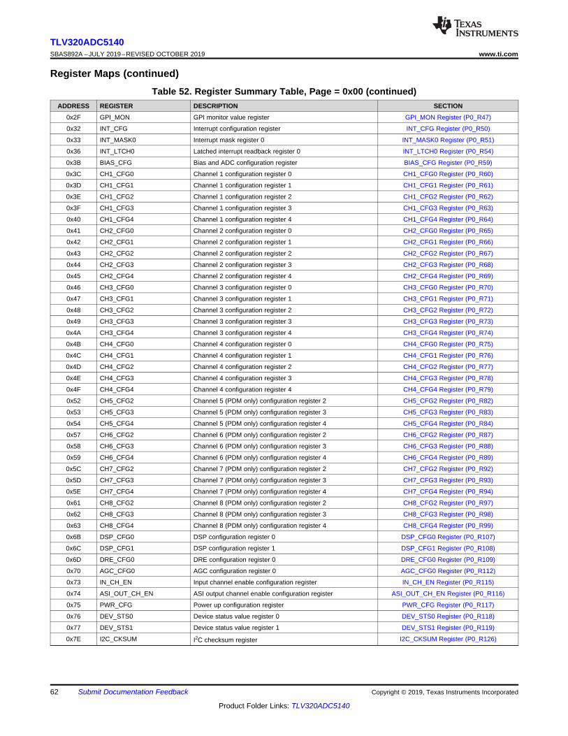
62
TLV320ADC5140SBAS892A –JULY 2019–REVISED OCTOBER 2019 www.ti.com
Product Folder Links: TLV320ADC5140
Submit Documentation Feedback Copyright © 2019, Texas Instruments Incorporated
Register Maps (continued)Table 52. Register Summary Table, Page = 0x00 (continued)
ADDRESS REGISTER DESCRIPTION SECTION
0x2F GPI_MON GPI monitor value register GPI_MON Register (P0_R47)
0x32 INT_CFG Interrupt configuration register INT_CFG Register (P0_R50)
0x33 INT_MASK0 Interrupt mask register 0 INT_MASK0 Register (P0_R51)
0x36 INT_LTCH0 Latched interrupt readback register 0 INT_LTCH0 Register (P0_R54)
0x3B BIAS_CFG Bias and ADC configuration register BIAS_CFG Register (P0_R59)
0x3C CH1_CFG0 Channel 1 configuration register 0 CH1_CFG0 Register (P0_R60)
0x3D CH1_CFG1 Channel 1 configuration register 1 CH1_CFG1 Register (P0_R61)
0x3E CH1_CFG2 Channel 1 configuration register 2 CH1_CFG2 Register (P0_R62)
0x3F CH1_CFG3 Channel 1 configuration register 3 CH1_CFG3 Register (P0_R63)
0x40 CH1_CFG4 Channel 1 configuration register 4 CH1_CFG4 Register (P0_R64)
0x41 CH2_CFG0 Channel 2 configuration register 0 CH2_CFG0 Register (P0_R65)
0x42 CH2_CFG1 Channel 2 configuration register 1 CH2_CFG1 Register (P0_R66)
0x43 CH2_CFG2 Channel 2 configuration register 2 CH2_CFG2 Register (P0_R67)
0x44 CH2_CFG3 Channel 2 configuration register 3 CH2_CFG3 Register (P0_R68)
0x45 CH2_CFG4 Channel 2 configuration register 4 CH2_CFG4 Register (P0_R69)
0x46 CH3_CFG0 Channel 3 configuration register 0 CH3_CFG0 Register (P0_R70)
0x47 CH3_CFG1 Channel 3 configuration register 1 CH3_CFG1 Register (P0_R71)
0x48 CH3_CFG2 Channel 3 configuration register 2 CH3_CFG2 Register (P0_R72)
0x49 CH3_CFG3 Channel 3 configuration register 3 CH3_CFG3 Register (P0_R73)
0x4A CH3_CFG4 Channel 3 configuration register 4 CH3_CFG4 Register (P0_R74)
0x4B CH4_CFG0 Channel 4 configuration register 0 CH4_CFG0 Register (P0_R75)
0x4C CH4_CFG1 Channel 4 configuration register 1 CH4_CFG1 Register (P0_R76)
0x4D CH4_CFG2 Channel 4 configuration register 2 CH4_CFG2 Register (P0_R77)
0x4E CH4_CFG3 Channel 4 configuration register 3 CH4_CFG3 Register (P0_R78)
0x4F CH4_CFG4 Channel 4 configuration register 4 CH4_CFG4 Register (P0_R79)
0x52 CH5_CFG2 Channel 5 (PDM only) configuration register 2 CH5_CFG2 Register (P0_R82)
0x53 CH5_CFG3 Channel 5 (PDM only) configuration register 3 CH5_CFG3 Register (P0_R83)
0x54 CH5_CFG4 Channel 5 (PDM only) configuration register 4 CH5_CFG4 Register (P0_R84)
0x57 CH6_CFG2 Channel 6 (PDM only) configuration register 2 CH6_CFG2 Register (P0_R87)
0x58 CH6_CFG3 Channel 6 (PDM only) configuration register 3 CH6_CFG3 Register (P0_R88)
0x59 CH6_CFG4 Channel 6 (PDM only) configuration register 4 CH6_CFG4 Register (P0_R89)
0x5C CH7_CFG2 Channel 7 (PDM only) configuration register 2 CH7_CFG2 Register (P0_R92)
0x5D CH7_CFG3 Channel 7 (PDM only) configuration register 3 CH7_CFG3 Register (P0_R93)
0x5E CH7_CFG4 Channel 7 (PDM only) configuration register 4 CH7_CFG4 Register (P0_R94)
0x61 CH8_CFG2 Channel 8 (PDM only) configuration register 2 CH8_CFG2 Register (P0_R97)
0x62 CH8_CFG3 Channel 8 (PDM only) configuration register 3 CH8_CFG3 Register (P0_R98)
0x63 CH8_CFG4 Channel 8 (PDM only) configuration register 4 CH8_CFG4 Register (P0_R99)
0x6B DSP_CFG0 DSP configuration register 0 DSP_CFG0 Register (P0_R107)
0x6C DSP_CFG1 DSP configuration register 1 DSP_CFG1 Register (P0_R108)
0x6D DRE_CFG0 DRE configuration register 0 DRE_CFG0 Register (P0_R109)
0x70 AGC_CFG0 AGC configuration register 0 AGC_CFG0 Register (P0_R112)
0x73 IN_CH_EN Input channel enable configuration register IN_CH_EN Register (P0_R115)
0x74 ASI_OUT_CH_EN ASI output channel enable configuration register ASI_OUT_CH_EN Register (P0_R116)
0x75 PWR_CFG Power up configuration register PWR_CFG Register (P0_R117)
0x76 DEV_STS0 Device status value register 0 DEV_STS0 Register (P0_R118)
0x77 DEV_STS1 Device status value register 1 DEV_STS1 Register (P0_R119)
0x7E I2C_CKSUM I2C checksum register I2C_CKSUM Register (P0_R126)
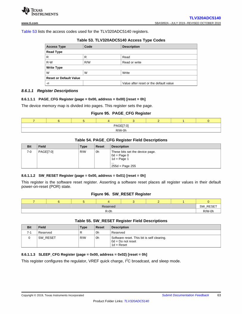
63
TLV320ADC5140www.ti.com SBAS892A –JULY 2019–REVISED OCTOBER 2019
Product Folder Links: TLV320ADC5140
Submit Documentation FeedbackCopyright © 2019, Texas Instruments Incorporated
Table 53 lists the access codes used for the TLV320ADC5140 registers.
Table 53. TLV320ADC5140 Access Type CodesAccess Type Code DescriptionRead TypeR R ReadR-W R/W Read or writeWrite TypeW W WriteReset or Default Value-n Value after reset or the default value
8.6.1.1 Register Descriptions
8.6.1.1.1 PAGE_CFG Register (page = 0x00, address = 0x00) [reset = 0h]
The device memory map is divided into pages. This register sets the page.
Figure 95. PAGE_CFG Register
7 6 5 4 3 2 1 0PAGE[7:0]
R/W-0h
Table 54. PAGE_CFG Register Field DescriptionsBit Field Type Reset Description7-0 PAGE[7:0] R/W 0h These bits set the device page.
0d = Page 01d = Page 1...255d = Page 255
8.6.1.1.2 SW_RESET Register (page = 0x00, address = 0x01) [reset = 0h]
This register is the software reset register. Asserting a software reset places all register values in their defaultpower-on-reset (POR) state.
Figure 96. SW_RESET Register
7 6 5 4 3 2 1 0Reserved SW_RESET
R-0h R/W-0h
Table 55. SW_RESET Register Field DescriptionsBit Field Type Reset Description7-1 Reserved R 0h Reserved0 SW_RESET R/W 0h Software reset. This bit is self clearing.
0d = Do not reset1d = Reset
8.6.1.1.3 SLEEP_CFG Register (page = 0x00, address = 0x02) [reset = 0h]
This register configures the regulator, VREF quick charge, I2C broadcast, and sleep mode.
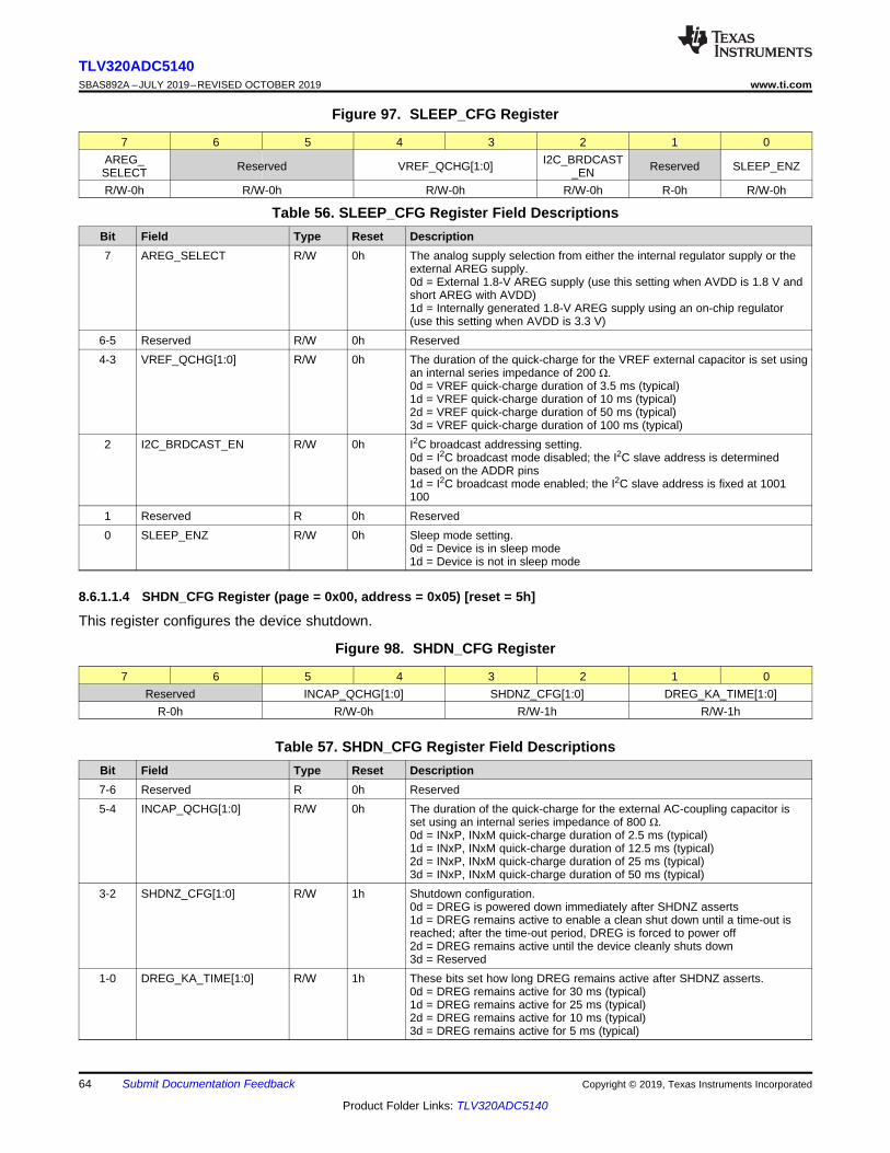
64
TLV320ADC5140SBAS892A –JULY 2019–REVISED OCTOBER 2019 www.ti.com
Product Folder Links: TLV320ADC5140
Submit Documentation Feedback Copyright © 2019, Texas Instruments Incorporated
Figure 97. SLEEP_CFG Register
7 6 5 4 3 2 1 0AREG_SELECT Reserved VREF_QCHG[1:0] I2C_BRDCAST
_EN Reserved SLEEP_ENZ
R/W-0h R/W-0h R/W-0h R/W-0h R-0h R/W-0h
Table 56. SLEEP_CFG Register Field DescriptionsBit Field Type Reset Description7 AREG_SELECT R/W 0h The analog supply selection from either the internal regulator supply or the
external AREG supply.0d = External 1.8-V AREG supply (use this setting when AVDD is 1.8 V andshort AREG with AVDD)1d = Internally generated 1.8-V AREG supply using an on-chip regulator(use this setting when AVDD is 3.3 V)
6-5 Reserved R/W 0h Reserved4-3 VREF_QCHG[1:0] R/W 0h The duration of the quick-charge for the VREF external capacitor is set using
an internal series impedance of 200 Ω.0d = VREF quick-charge duration of 3.5 ms (typical)1d = VREF quick-charge duration of 10 ms (typical)2d = VREF quick-charge duration of 50 ms (typical)3d = VREF quick-charge duration of 100 ms (typical)
2 I2C_BRDCAST_EN R/W 0h I2C broadcast addressing setting.0d = I2C broadcast mode disabled; the I2C slave address is determinedbased on the ADDR pins1d = I2C broadcast mode enabled; the I2C slave address is fixed at 1001100
1 Reserved R 0h Reserved0 SLEEP_ENZ R/W 0h Sleep mode setting.
0d = Device is in sleep mode1d = Device is not in sleep mode
8.6.1.1.4 SHDN_CFG Register (page = 0x00, address = 0x05) [reset = 5h]
This register configures the device shutdown.
Figure 98. SHDN_CFG Register
7 6 5 4 3 2 1 0Reserved INCAP_QCHG[1:0] SHDNZ_CFG[1:0] DREG_KA_TIME[1:0]
R-0h R/W-0h R/W-1h R/W-1h
Table 57. SHDN_CFG Register Field DescriptionsBit Field Type Reset Description7-6 Reserved R 0h Reserved5-4 INCAP_QCHG[1:0] R/W 0h The duration of the quick-charge for the external AC-coupling capacitor is
set using an internal series impedance of 800 Ω.0d = INxP, INxM quick-charge duration of 2.5 ms (typical)1d = INxP, INxM quick-charge duration of 12.5 ms (typical)2d = INxP, INxM quick-charge duration of 25 ms (typical)3d = INxP, INxM quick-charge duration of 50 ms (typical)
3-2 SHDNZ_CFG[1:0] R/W 1h Shutdown configuration.0d = DREG is powered down immediately after SHDNZ asserts1d = DREG remains active to enable a clean shut down until a time-out isreached; after the time-out period, DREG is forced to power off2d = DREG remains active until the device cleanly shuts down3d = Reserved
1-0 DREG_KA_TIME[1:0] R/W 1h These bits set how long DREG remains active after SHDNZ asserts.0d = DREG remains active for 30 ms (typical)1d = DREG remains active for 25 ms (typical)2d = DREG remains active for 10 ms (typical)3d = DREG remains active for 5 ms (typical)
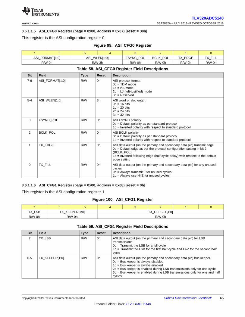
65
TLV320ADC5140www.ti.com SBAS892A –JULY 2019–REVISED OCTOBER 2019
Product Folder Links: TLV320ADC5140
Submit Documentation FeedbackCopyright © 2019, Texas Instruments Incorporated
8.6.1.1.5 ASI_CFG0 Register (page = 0x00, address = 0x07) [reset = 30h]
This register is the ASI configuration register 0.
Figure 99. ASI_CFG0 Register
7 6 5 4 3 2 1 0ASI_FORMAT[1:0] ASI_WLEN[1:0] FSYNC_POL BCLK_POL TX_EDGE TX_FILL
R/W-0h R/W-3h R/W-0h R/W-0h R/W-0h R/W-0h
Table 58. ASI_CFG0 Register Field DescriptionsBit Field Type Reset Description7-6 ASI_FORMAT[1:0] R/W 0h ASI protocol format.
0d = TDM mode1d = I2S mode2d = LJ (left-justified) mode3d = Reserved
5-4 ASI_WLEN[1:0] R/W 3h ASI word or slot length.0d = 16 bits1d = 20 bits2d = 24 bits3d = 32 bits
3 FSYNC_POL R/W 0h ASI FSYNC polarity.0d = Default polarity as per standard protocol1d = Inverted polarity with respect to standard protocol
2 BCLK_POL R/W 0h ASI BCLK polarity.0d = Default polarity as per standard protocol1d = Inverted polarity with respect to standard protocol
1 TX_EDGE R/W 0h ASI data output (on the primary and secondary data pin) transmit edge.0d = Default edge as per the protocol configuration setting in bit 2(BCLK_POL)1d = Inverted following edge (half cycle delay) with respect to the defaultedge setting
0 TX_FILL R/W 0h ASI data output (on the primary and secondary data pin) for any unusedcycles0d = Always transmit 0 for unused cycles1d = Always use Hi-Z for unused cycles
8.6.1.1.6 ASI_CFG1 Register (page = 0x00, address = 0x08) [reset = 0h]
This register is the ASI configuration register 1.
Figure 100. ASI_CFG1 Register
7 6 5 4 3 2 1 0TX_LSB TX_KEEPER[1:0] TX_OFFSET[4:0]R/W-0h R/W-0h R/W-0h
Table 59. ASI_CFG1 Register Field DescriptionsBit Field Type Reset Description7 TX_LSB R/W 0h ASI data output (on the primary and secondary data pin) for LSB
transmissions.0d = Transmit the LSB for a full cycle1d = Transmit the LSB for the first half cycle and Hi-Z for the second halfcycle
6-5 TX_KEEPER[1:0] R/W 0h ASI data output (on the primary and secondary data pin) bus keeper.0d = Bus keeper is always disabled1d = Bus keeper is always enabled2d = Bus keeper is enabled during LSB transmissions only for one cycle3d = Bus keeper is enabled during LSB transmissions only for one and halfcycles
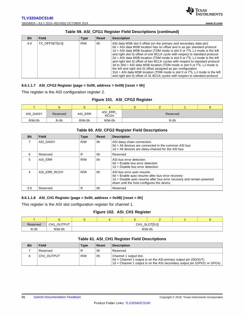
66
TLV320ADC5140SBAS892A –JULY 2019–REVISED OCTOBER 2019 www.ti.com
Product Folder Links: TLV320ADC5140
Submit Documentation Feedback Copyright © 2019, Texas Instruments Incorporated
Table 59. ASI_CFG1 Register Field Descriptions (continued)Bit Field Type Reset Description4-0 TX_OFFSET[4:0] R/W 0h ASI data MSB slot 0 offset (on the primary and secondary data pin).
0d = ASI data MSB location has no offset and is as per standard protocol1d = ASI data MSB location (TDM mode is slot 0 or I2S, LJ mode is the leftand right slot 0) offset of one BCLK cycle with respect to standard protocol2d = ASI data MSB location (TDM mode is slot 0 or I2S, LJ mode is the leftand right slot 0) offset of two BCLK cycles with respect to standard protocol3d to 30d = ASI data MSB location (TDM mode is slot 0 or I2S, LJ mode isthe left and right slot 0) offset assigned as per configuration31d = ASI data MSB location (TDM mode is slot 0 or I2S, LJ mode is the leftand right slot 0) offset of 31 BCLK cycles with respect to standard protocol
8.6.1.1.7 ASI_CFG2 Register (page = 0x00, address = 0x09) [reset = 0h]
This register is the ASI configuration register 2.
Figure 101. ASI_CFG2 Register
7 6 5 4 3 2 1 0
ASI_DAISY Reserved ASI_ERR ASI_ERR_RCOV Reserved
R/W-0h R-0h R/W-0h R/W-0h R-0h
Table 60. ASI_CFG2 Register Field DescriptionsBit Field Type Reset Description7 ASI_DAISY R/W 0h ASI daisy-chain connection.
0d = All devices are connected in the common ASI bus1d = All devices are daisy-chained for the ASI bus
6 Reserved R 0h Reserved5 ASI_ERR R/W 0h ASI bus error detection.
0d = Enable bus error detection1d = Disable bus error detection
4 ASI_ERR_RCOV R/W 0h ASI bus error auto resume.0d = Enable auto resume after bus error recovery1d = Disable auto resume after bus error recovery and remain powereddown until the host configures the device
3-0 Reserved R 0h Reserved
8.6.1.1.8 ASI_CH1 Register (page = 0x00, address = 0x0B) [reset = 0h]
This register is the ASI slot configuration register for channel 1.
Figure 102. ASI_CH1 Register
7 6 5 4 3 2 1 0Reserved CH1_OUTPUT CH1_SLOT[5:0]
R-0h R/W-0h R/W-0h
Table 61. ASI_CH1 Register Field DescriptionsBit Field Type Reset Description7 Reserved R 0h Reserved6 CH1_OUTPUT R/W 0h Channel 1 output line.
0d = Channel 1 output is on the ASI primary output pin (SDOUT)1d = Channel 1 output is on the ASI secondary output pin (GPIO1 or GPOx)

67
TLV320ADC5140www.ti.com SBAS892A –JULY 2019–REVISED OCTOBER 2019
Product Folder Links: TLV320ADC5140
Submit Documentation FeedbackCopyright © 2019, Texas Instruments Incorporated
Table 61. ASI_CH1 Register Field Descriptions (continued)Bit Field Type Reset Description5-0 CH1_SLOT[5:0] R/W 0h Channel 1 slot assignment.
0d = TDM is slot 0 or I2S, LJ is left slot 01d = TDM is slot 1 or I2S, LJ is left slot 12d to 30d = Slot assigned as per configuration31d = TDM is slot 31 or I2S, LJ is left slot 3132d = TDM is slot 32 or I2S, LJ is right slot 033d = TDM is slot 33 or I2S, LJ is right slot 134d to 62d = Slot assigned as per configuration63d = TDM is slot 63 or I2S, LJ is right slot 31
8.6.1.1.9 ASI_CH2 Register (page = 0x00, address = 0x0C) [reset = 1h]
This register is the ASI slot configuration register for channel 2.
Figure 103. ASI_CH2 Register
7 6 5 4 3 2 1 0Reserved CH2_OUTPUT CH2_SLOT[5:0]
R-0h R/W-0h R/W-1h
Table 62. ASI_CH2 Register Field DescriptionsBit Field Type Reset Description7 Reserved R 0h Reserved6 CH2_OUTPUT R/W 0h Channel 2 output line.
0d = Channel 2 output is on the ASI primary output pin (SDOUT)1d = Channel 2 output is on the ASI secondary output pin (GPIO1 or GPOx)
5-0 CH2_SLOT[5:0] R/W 1h Channel 2 slot assignment.0d = TDM is slot 0 or I2S, LJ is left slot 01d = TDM is slot 1 or I2S, LJ is left slot 12d to 30d = Slot assigned as per configuration31d = TDM is slot 31 or I2S, LJ is left slot 3132d = TDM is slot 32 or I2S, LJ is right slot 033d = TDM is slot 33 or I2S, LJ is right slot 134d to 62d = Slot assigned as per configuration63d = TDM is slot 63 or I2S, LJ is right slot 31
8.6.1.1.10 ASI_CH3 Register (page = 0x00, address = 0x0D) [reset = 2h]
This register is the ASI slot configuration register for channel 3.
Figure 104. ASI_CH3 Register
7 6 5 4 3 2 1 0Reserved CH3_OUTPUT CH3_SLOT[5:0]
R-0h R/W-0h R/W-2h
Table 63. ASI_CH3 Register Field DescriptionsBit Field Type Reset Description7 Reserved R 0h Reserved6 CH3_OUTPUT R/W 0h Channel 3 output line.
0d = Channel 3 output is on the ASI primary output pin (SDOUT)1d = Channel 3 output is on the ASI secondary output pin (GPIO1 or GPOx)
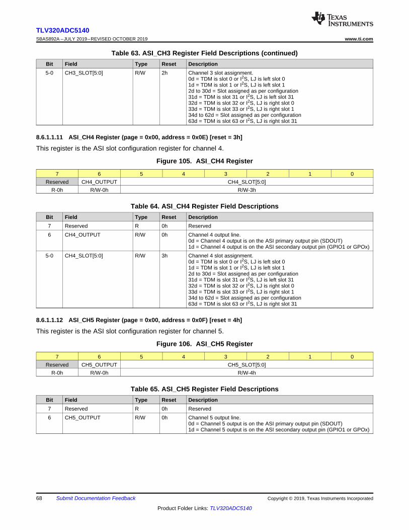
68
TLV320ADC5140SBAS892A –JULY 2019–REVISED OCTOBER 2019 www.ti.com
Product Folder Links: TLV320ADC5140
Submit Documentation Feedback Copyright © 2019, Texas Instruments Incorporated
Table 63. ASI_CH3 Register Field Descriptions (continued)Bit Field Type Reset Description5-0 CH3_SLOT[5:0] R/W 2h Channel 3 slot assignment.
0d = TDM is slot 0 or I2S, LJ is left slot 01d = TDM is slot 1 or I2S, LJ is left slot 12d to 30d = Slot assigned as per configuration31d = TDM is slot 31 or I2S, LJ is left slot 3132d = TDM is slot 32 or I2S, LJ is right slot 033d = TDM is slot 33 or I2S, LJ is right slot 134d to 62d = Slot assigned as per configuration63d = TDM is slot 63 or I2S, LJ is right slot 31
8.6.1.1.11 ASI_CH4 Register (page = 0x00, address = 0x0E) [reset = 3h]
This register is the ASI slot configuration register for channel 4.
Figure 105. ASI_CH4 Register
7 6 5 4 3 2 1 0Reserved CH4_OUTPUT CH4_SLOT[5:0]
R-0h R/W-0h R/W-3h
Table 64. ASI_CH4 Register Field DescriptionsBit Field Type Reset Description7 Reserved R 0h Reserved6 CH4_OUTPUT R/W 0h Channel 4 output line.
0d = Channel 4 output is on the ASI primary output pin (SDOUT)1d = Channel 4 output is on the ASI secondary output pin (GPIO1 or GPOx)
5-0 CH4_SLOT[5:0] R/W 3h Channel 4 slot assignment.0d = TDM is slot 0 or I2S, LJ is left slot 01d = TDM is slot 1 or I2S, LJ is left slot 12d to 30d = Slot assigned as per configuration31d = TDM is slot 31 or I2S, LJ is left slot 3132d = TDM is slot 32 or I2S, LJ is right slot 033d = TDM is slot 33 or I2S, LJ is right slot 134d to 62d = Slot assigned as per configuration63d = TDM is slot 63 or I2S, LJ is right slot 31
8.6.1.1.12 ASI_CH5 Register (page = 0x00, address = 0x0F) [reset = 4h]
This register is the ASI slot configuration register for channel 5.
Figure 106. ASI_CH5 Register
7 6 5 4 3 2 1 0Reserved CH5_OUTPUT CH5_SLOT[5:0]
R-0h R/W-0h R/W-4h
Table 65. ASI_CH5 Register Field DescriptionsBit Field Type Reset Description7 Reserved R 0h Reserved6 CH5_OUTPUT R/W 0h Channel 5 output line.
0d = Channel 5 output is on the ASI primary output pin (SDOUT)1d = Channel 5 output is on the ASI secondary output pin (GPIO1 or GPOx)
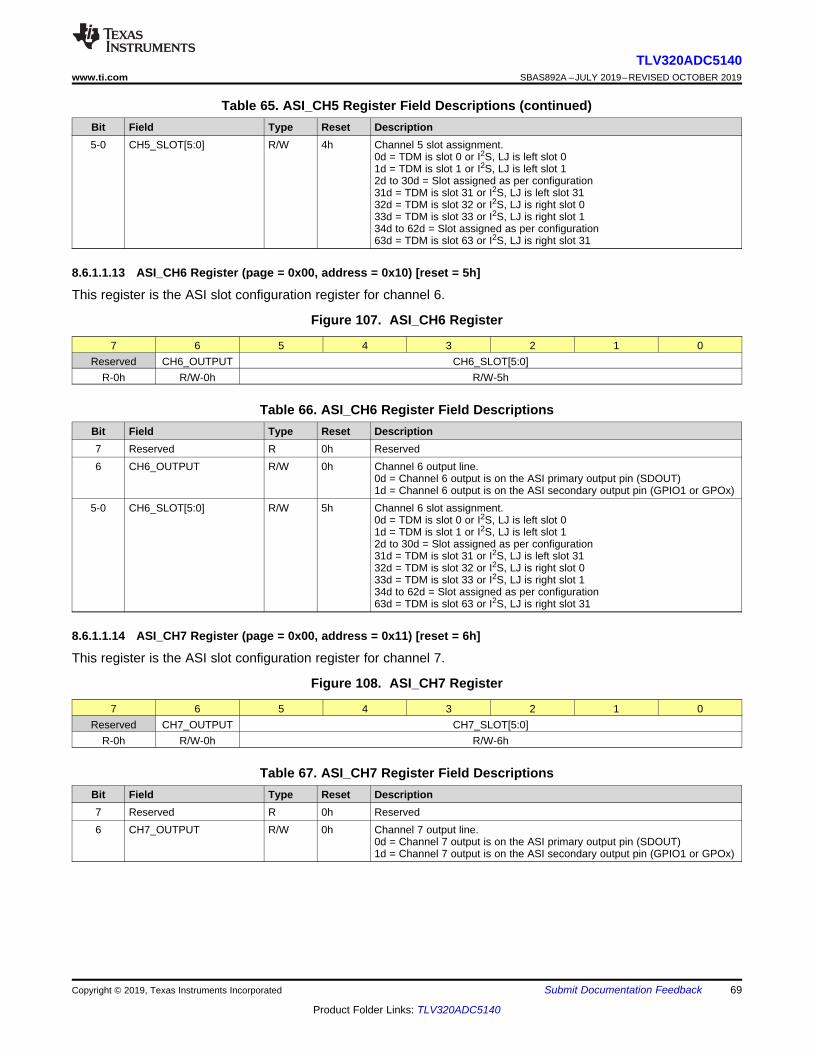
69
TLV320ADC5140www.ti.com SBAS892A –JULY 2019–REVISED OCTOBER 2019
Product Folder Links: TLV320ADC5140
Submit Documentation FeedbackCopyright © 2019, Texas Instruments Incorporated
Table 65. ASI_CH5 Register Field Descriptions (continued)Bit Field Type Reset Description5-0 CH5_SLOT[5:0] R/W 4h Channel 5 slot assignment.
0d = TDM is slot 0 or I2S, LJ is left slot 01d = TDM is slot 1 or I2S, LJ is left slot 12d to 30d = Slot assigned as per configuration31d = TDM is slot 31 or I2S, LJ is left slot 3132d = TDM is slot 32 or I2S, LJ is right slot 033d = TDM is slot 33 or I2S, LJ is right slot 134d to 62d = Slot assigned as per configuration63d = TDM is slot 63 or I2S, LJ is right slot 31
8.6.1.1.13 ASI_CH6 Register (page = 0x00, address = 0x10) [reset = 5h]
This register is the ASI slot configuration register for channel 6.
Figure 107. ASI_CH6 Register
7 6 5 4 3 2 1 0Reserved CH6_OUTPUT CH6_SLOT[5:0]
R-0h R/W-0h R/W-5h
Table 66. ASI_CH6 Register Field DescriptionsBit Field Type Reset Description7 Reserved R 0h Reserved6 CH6_OUTPUT R/W 0h Channel 6 output line.
0d = Channel 6 output is on the ASI primary output pin (SDOUT)1d = Channel 6 output is on the ASI secondary output pin (GPIO1 or GPOx)
5-0 CH6_SLOT[5:0] R/W 5h Channel 6 slot assignment.0d = TDM is slot 0 or I2S, LJ is left slot 01d = TDM is slot 1 or I2S, LJ is left slot 12d to 30d = Slot assigned as per configuration31d = TDM is slot 31 or I2S, LJ is left slot 3132d = TDM is slot 32 or I2S, LJ is right slot 033d = TDM is slot 33 or I2S, LJ is right slot 134d to 62d = Slot assigned as per configuration63d = TDM is slot 63 or I2S, LJ is right slot 31
8.6.1.1.14 ASI_CH7 Register (page = 0x00, address = 0x11) [reset = 6h]
This register is the ASI slot configuration register for channel 7.
Figure 108. ASI_CH7 Register
7 6 5 4 3 2 1 0Reserved CH7_OUTPUT CH7_SLOT[5:0]
R-0h R/W-0h R/W-6h
Table 67. ASI_CH7 Register Field DescriptionsBit Field Type Reset Description7 Reserved R 0h Reserved6 CH7_OUTPUT R/W 0h Channel 7 output line.
0d = Channel 7 output is on the ASI primary output pin (SDOUT)1d = Channel 7 output is on the ASI secondary output pin (GPIO1 or GPOx)
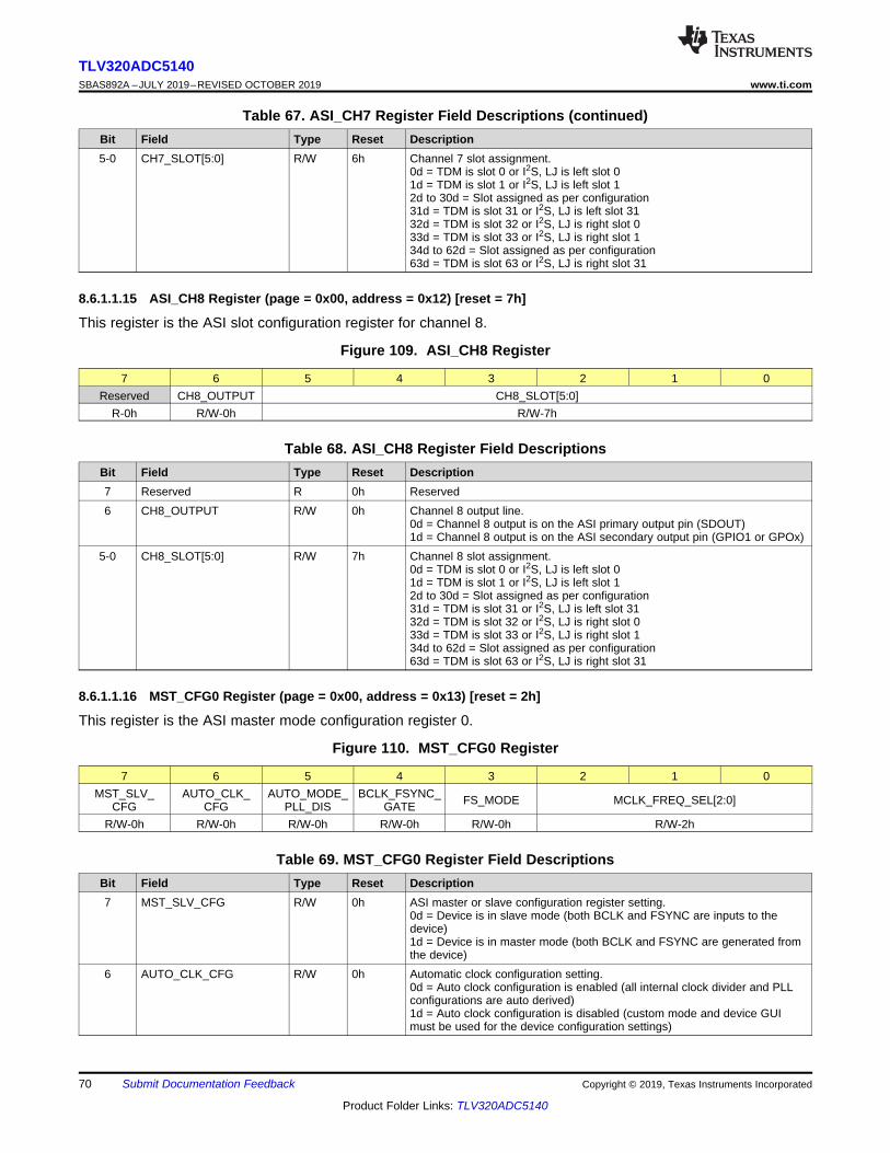
70
TLV320ADC5140SBAS892A –JULY 2019–REVISED OCTOBER 2019 www.ti.com
Product Folder Links: TLV320ADC5140
Submit Documentation Feedback Copyright © 2019, Texas Instruments Incorporated
Table 67. ASI_CH7 Register Field Descriptions (continued)Bit Field Type Reset Description5-0 CH7_SLOT[5:0] R/W 6h Channel 7 slot assignment.
0d = TDM is slot 0 or I2S, LJ is left slot 01d = TDM is slot 1 or I2S, LJ is left slot 12d to 30d = Slot assigned as per configuration31d = TDM is slot 31 or I2S, LJ is left slot 3132d = TDM is slot 32 or I2S, LJ is right slot 033d = TDM is slot 33 or I2S, LJ is right slot 134d to 62d = Slot assigned as per configuration63d = TDM is slot 63 or I2S, LJ is right slot 31
8.6.1.1.15 ASI_CH8 Register (page = 0x00, address = 0x12) [reset = 7h]
This register is the ASI slot configuration register for channel 8.
Figure 109. ASI_CH8 Register
7 6 5 4 3 2 1 0Reserved CH8_OUTPUT CH8_SLOT[5:0]
R-0h R/W-0h R/W-7h
Table 68. ASI_CH8 Register Field DescriptionsBit Field Type Reset Description7 Reserved R 0h Reserved6 CH8_OUTPUT R/W 0h Channel 8 output line.
0d = Channel 8 output is on the ASI primary output pin (SDOUT)1d = Channel 8 output is on the ASI secondary output pin (GPIO1 or GPOx)
5-0 CH8_SLOT[5:0] R/W 7h Channel 8 slot assignment.0d = TDM is slot 0 or I2S, LJ is left slot 01d = TDM is slot 1 or I2S, LJ is left slot 12d to 30d = Slot assigned as per configuration31d = TDM is slot 31 or I2S, LJ is left slot 3132d = TDM is slot 32 or I2S, LJ is right slot 033d = TDM is slot 33 or I2S, LJ is right slot 134d to 62d = Slot assigned as per configuration63d = TDM is slot 63 or I2S, LJ is right slot 31
8.6.1.1.16 MST_CFG0 Register (page = 0x00, address = 0x13) [reset = 2h]
This register is the ASI master mode configuration register 0.
Figure 110. MST_CFG0 Register
7 6 5 4 3 2 1 0MST_SLV_
CFGAUTO_CLK_
CFGAUTO_MODE_
PLL_DISBCLK_FSYNC_
GATE FS_MODE MCLK_FREQ_SEL[2:0]
R/W-0h R/W-0h R/W-0h R/W-0h R/W-0h R/W-2h
Table 69. MST_CFG0 Register Field DescriptionsBit Field Type Reset Description7 MST_SLV_CFG R/W 0h ASI master or slave configuration register setting.
0d = Device is in slave mode (both BCLK and FSYNC are inputs to thedevice)1d = Device is in master mode (both BCLK and FSYNC are generated fromthe device)
6 AUTO_CLK_CFG R/W 0h Automatic clock configuration setting.0d = Auto clock configuration is enabled (all internal clock divider and PLLconfigurations are auto derived)1d = Auto clock configuration is disabled (custom mode and device GUImust be used for the device configuration settings)
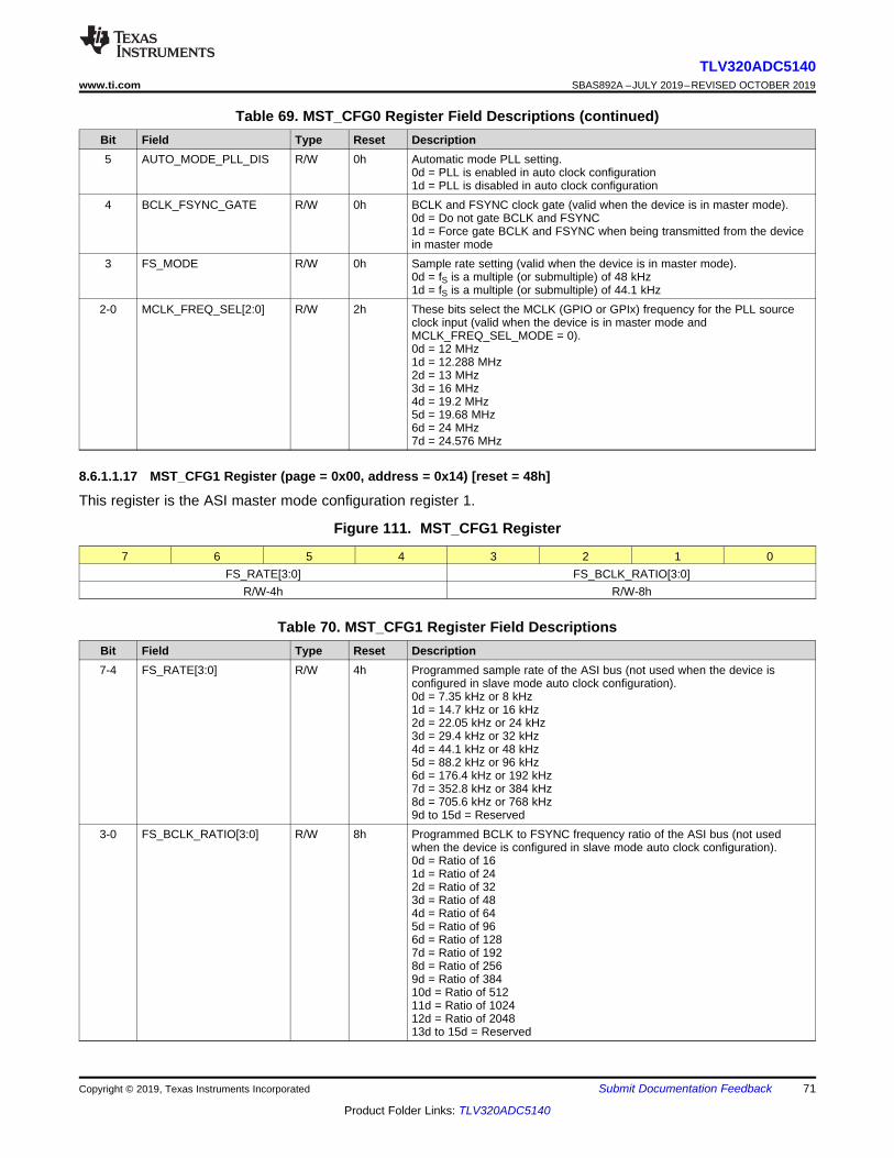
71
TLV320ADC5140www.ti.com SBAS892A –JULY 2019–REVISED OCTOBER 2019
Product Folder Links: TLV320ADC5140
Submit Documentation FeedbackCopyright © 2019, Texas Instruments Incorporated
Table 69. MST_CFG0 Register Field Descriptions (continued)Bit Field Type Reset Description5 AUTO_MODE_PLL_DIS R/W 0h Automatic mode PLL setting.
0d = PLL is enabled in auto clock configuration1d = PLL is disabled in auto clock configuration
4 BCLK_FSYNC_GATE R/W 0h BCLK and FSYNC clock gate (valid when the device is in master mode).0d = Do not gate BCLK and FSYNC1d = Force gate BCLK and FSYNC when being transmitted from the devicein master mode
3 FS_MODE R/W 0h Sample rate setting (valid when the device is in master mode).0d = fS is a multiple (or submultiple) of 48 kHz1d = fS is a multiple (or submultiple) of 44.1 kHz
2-0 MCLK_FREQ_SEL[2:0] R/W 2h These bits select the MCLK (GPIO or GPIx) frequency for the PLL sourceclock input (valid when the device is in master mode andMCLK_FREQ_SEL_MODE = 0).0d = 12 MHz1d = 12.288 MHz2d = 13 MHz3d = 16 MHz4d = 19.2 MHz5d = 19.68 MHz6d = 24 MHz7d = 24.576 MHz
8.6.1.1.17 MST_CFG1 Register (page = 0x00, address = 0x14) [reset = 48h]
This register is the ASI master mode configuration register 1.
Figure 111. MST_CFG1 Register
7 6 5 4 3 2 1 0FS_RATE[3:0] FS_BCLK_RATIO[3:0]
R/W-4h R/W-8h
Table 70. MST_CFG1 Register Field DescriptionsBit Field Type Reset Description7-4 FS_RATE[3:0] R/W 4h Programmed sample rate of the ASI bus (not used when the device is
configured in slave mode auto clock configuration).0d = 7.35 kHz or 8 kHz1d = 14.7 kHz or 16 kHz2d = 22.05 kHz or 24 kHz3d = 29.4 kHz or 32 kHz4d = 44.1 kHz or 48 kHz5d = 88.2 kHz or 96 kHz6d = 176.4 kHz or 192 kHz7d = 352.8 kHz or 384 kHz8d = 705.6 kHz or 768 kHz9d to 15d = Reserved
3-0 FS_BCLK_RATIO[3:0] R/W 8h Programmed BCLK to FSYNC frequency ratio of the ASI bus (not usedwhen the device is configured in slave mode auto clock configuration).0d = Ratio of 161d = Ratio of 242d = Ratio of 323d = Ratio of 484d = Ratio of 645d = Ratio of 966d = Ratio of 1287d = Ratio of 1928d = Ratio of 2569d = Ratio of 38410d = Ratio of 51211d = Ratio of 102412d = Ratio of 204813d to 15d = Reserved
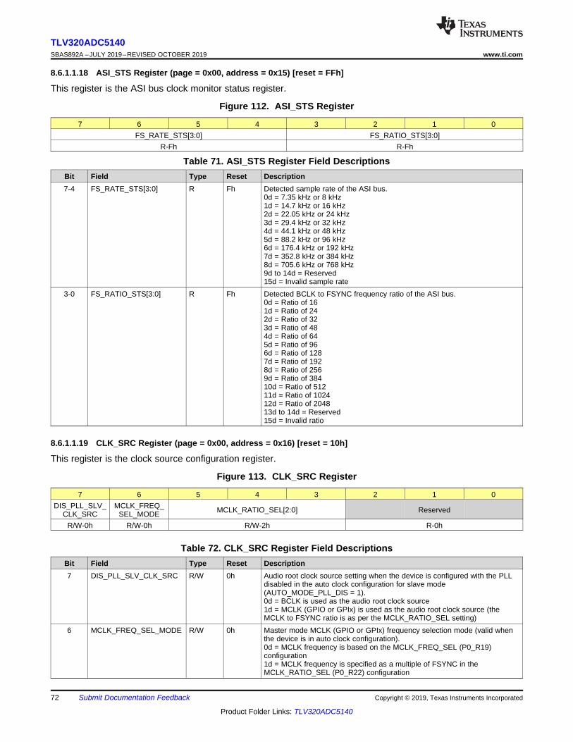
72
TLV320ADC5140SBAS892A –JULY 2019–REVISED OCTOBER 2019 www.ti.com
Product Folder Links: TLV320ADC5140
Submit Documentation Feedback Copyright © 2019, Texas Instruments Incorporated
8.6.1.1.18 ASI_STS Register (page = 0x00, address = 0x15) [reset = FFh]
This register is the ASI bus clock monitor status register.
Figure 112. ASI_STS Register
7 6 5 4 3 2 1 0FS_RATE_STS[3:0] FS_RATIO_STS[3:0]
R-Fh R-Fh
Table 71. ASI_STS Register Field DescriptionsBit Field Type Reset Description7-4 FS_RATE_STS[3:0] R Fh Detected sample rate of the ASI bus.
0d = 7.35 kHz or 8 kHz1d = 14.7 kHz or 16 kHz2d = 22.05 kHz or 24 kHz3d = 29.4 kHz or 32 kHz4d = 44.1 kHz or 48 kHz5d = 88.2 kHz or 96 kHz6d = 176.4 kHz or 192 kHz7d = 352.8 kHz or 384 kHz8d = 705.6 kHz or 768 kHz9d to 14d = Reserved15d = Invalid sample rate
3-0 FS_RATIO_STS[3:0] R Fh Detected BCLK to FSYNC frequency ratio of the ASI bus.0d = Ratio of 161d = Ratio of 242d = Ratio of 323d = Ratio of 484d = Ratio of 645d = Ratio of 966d = Ratio of 1287d = Ratio of 1928d = Ratio of 2569d = Ratio of 38410d = Ratio of 51211d = Ratio of 102412d = Ratio of 204813d to 14d = Reserved15d = Invalid ratio
8.6.1.1.19 CLK_SRC Register (page = 0x00, address = 0x16) [reset = 10h]
This register is the clock source configuration register.
Figure 113. CLK_SRC Register
7 6 5 4 3 2 1 0DIS_PLL_SLV_
CLK_SRCMCLK_FREQ_
SEL_MODE MCLK_RATIO_SEL[2:0] Reserved
R/W-0h R/W-0h R/W-2h R-0h
Table 72. CLK_SRC Register Field DescriptionsBit Field Type Reset Description7 DIS_PLL_SLV_CLK_SRC R/W 0h Audio root clock source setting when the device is configured with the PLL
disabled in the auto clock configuration for slave mode(AUTO_MODE_PLL_DIS = 1).0d = BCLK is used as the audio root clock source1d = MCLK (GPIO or GPIx) is used as the audio root clock source (theMCLK to FSYNC ratio is as per the MCLK_RATIO_SEL setting)
6 MCLK_FREQ_SEL_MODE R/W 0h Master mode MCLK (GPIO or GPIx) frequency selection mode (valid whenthe device is in auto clock configuration).0d = MCLK frequency is based on the MCLK_FREQ_SEL (P0_R19)configuration1d = MCLK frequency is specified as a multiple of FSYNC in theMCLK_RATIO_SEL (P0_R22) configuration
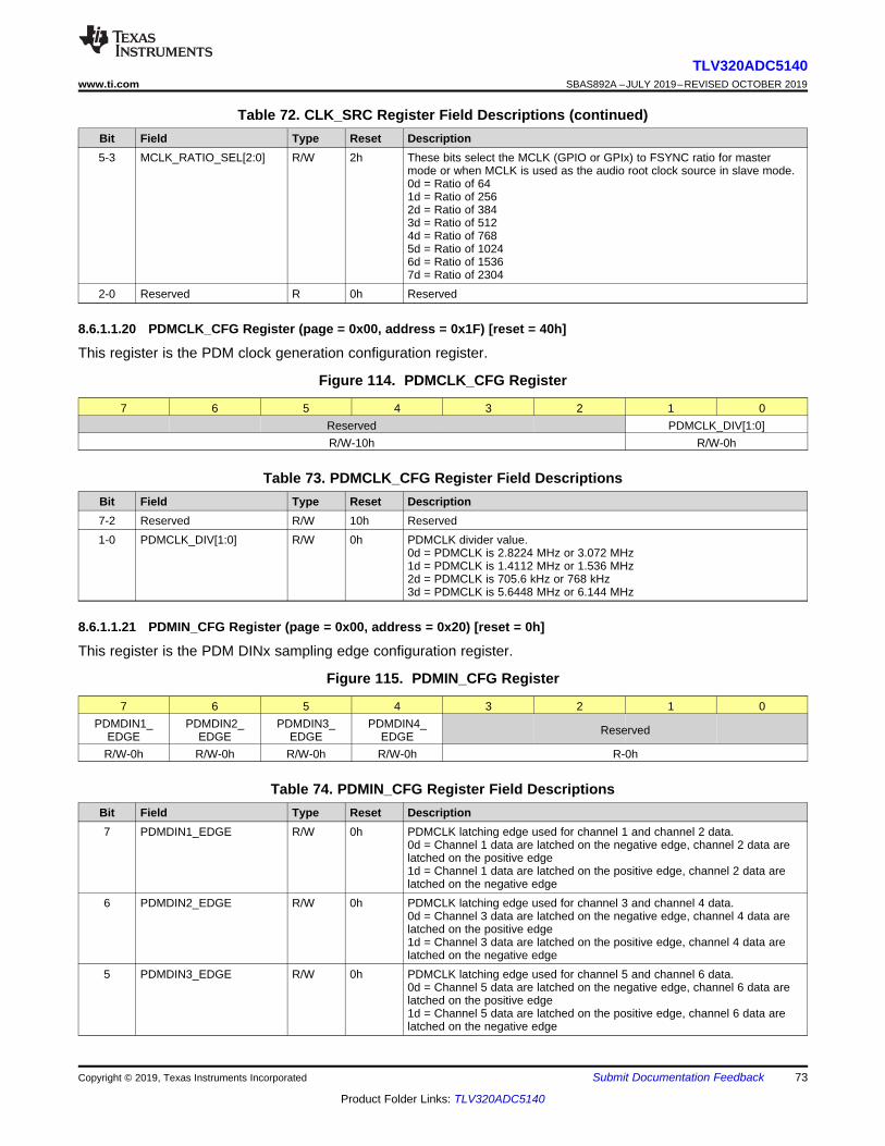
73
TLV320ADC5140www.ti.com SBAS892A –JULY 2019–REVISED OCTOBER 2019
Product Folder Links: TLV320ADC5140
Submit Documentation FeedbackCopyright © 2019, Texas Instruments Incorporated
Table 72. CLK_SRC Register Field Descriptions (continued)Bit Field Type Reset Description5-3 MCLK_RATIO_SEL[2:0] R/W 2h These bits select the MCLK (GPIO or GPIx) to FSYNC ratio for master
mode or when MCLK is used as the audio root clock source in slave mode.0d = Ratio of 641d = Ratio of 2562d = Ratio of 3843d = Ratio of 5124d = Ratio of 7685d = Ratio of 10246d = Ratio of 15367d = Ratio of 2304
2-0 Reserved R 0h Reserved
8.6.1.1.20 PDMCLK_CFG Register (page = 0x00, address = 0x1F) [reset = 40h]
This register is the PDM clock generation configuration register.
Figure 114. PDMCLK_CFG Register
7 6 5 4 3 2 1 0Reserved PDMCLK_DIV[1:0]R/W-10h R/W-0h
Table 73. PDMCLK_CFG Register Field DescriptionsBit Field Type Reset Description7-2 Reserved R/W 10h Reserved1-0 PDMCLK_DIV[1:0] R/W 0h PDMCLK divider value.
0d = PDMCLK is 2.8224 MHz or 3.072 MHz1d = PDMCLK is 1.4112 MHz or 1.536 MHz2d = PDMCLK is 705.6 kHz or 768 kHz3d = PDMCLK is 5.6448 MHz or 6.144 MHz
8.6.1.1.21 PDMIN_CFG Register (page = 0x00, address = 0x20) [reset = 0h]
This register is the PDM DINx sampling edge configuration register.
Figure 115. PDMIN_CFG Register
7 6 5 4 3 2 1 0PDMDIN1_
EDGEPDMDIN2_
EDGEPDMDIN3_
EDGEPDMDIN4_
EDGE Reserved
R/W-0h R/W-0h R/W-0h R/W-0h R-0h
Table 74. PDMIN_CFG Register Field DescriptionsBit Field Type Reset Description7 PDMDIN1_EDGE R/W 0h PDMCLK latching edge used for channel 1 and channel 2 data.
0d = Channel 1 data are latched on the negative edge, channel 2 data arelatched on the positive edge1d = Channel 1 data are latched on the positive edge, channel 2 data arelatched on the negative edge
6 PDMDIN2_EDGE R/W 0h PDMCLK latching edge used for channel 3 and channel 4 data.0d = Channel 3 data are latched on the negative edge, channel 4 data arelatched on the positive edge1d = Channel 3 data are latched on the positive edge, channel 4 data arelatched on the negative edge
5 PDMDIN3_EDGE R/W 0h PDMCLK latching edge used for channel 5 and channel 6 data.0d = Channel 5 data are latched on the negative edge, channel 6 data arelatched on the positive edge1d = Channel 5 data are latched on the positive edge, channel 6 data arelatched on the negative edge
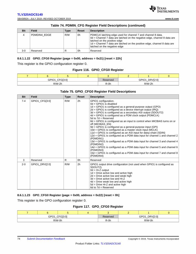
74
TLV320ADC5140SBAS892A –JULY 2019–REVISED OCTOBER 2019 www.ti.com
Product Folder Links: TLV320ADC5140
Submit Documentation Feedback Copyright © 2019, Texas Instruments Incorporated
Table 74. PDMIN_CFG Register Field Descriptions (continued)Bit Field Type Reset Description4 PDMDIN4_EDGE R/W 0h PDMCLK latching edge used for channel 7 and channel 8 data.
0d = Channel 7 data are latched on the negative edge, channel 8 data arelatched on the positive edge1d = Channel 7 data are latched on the positive edge, channel 8 data arelatched on the negative edge
3-0 Reserved R 0h Reserved
8.6.1.1.22 GPIO_CFG0 Register (page = 0x00, address = 0x21) [reset = 22h]
This register is the GPIO configuration register 0.
Figure 116. GPIO_CFG0 Register
7 6 5 4 3 2 1 0GPIO1_CFG[3:0] Reserved GPIO1_DRV[2:0]
R/W-2h R-0h R/W-2h
Table 75. GPIO_CFG0 Register Field DescriptionsBit Field Type Reset Description7-4 GPIO1_CFG[3:0] R/W 2h GPIO1 configuration.
0d = GPIO1 is disabled1d = GPIO1 is configured as a general-purpose output (GPO)2d = GPIO1 is configured as a device interrupt output (IRQ)3d = GPIO1 is configured as a secondary ASI output (SDOUT2)4d = GPIO1 is configured as a PDM clock output (PDMCLK)5d to 7d = Reserved8d = GPIO1 is configured as an input to control when MICBIAS turns on oroff (MICBIAS_EN)9d = GPIO1 is configured as a general-purpose input (GPI)10d = GPIO1 is configured as a master clock input (MCLK)11d = GPIO1 is configured as an ASI input for daisy-chain (SDIN)12d = GPIO1 is configured as a PDM data input for channel 1 and channel 2(PDMDIN1)13d = GPIO1 is configured as a PDM data input for channel 3 and channel 4(PDMDIN2)14d = GPIO1 is configured as a PDM data input for channel 5 and channel 6(PDMDIN3)15d = GPIO1 is configured as a PDM data input for channel 7 and channel 8(PDMDIN4)
3 Reserved R 0h Reserved2-0 GPIO1_DRV[2:0] R/W 2h GPIO1 output drive configuration (not used when GPIO1 is configured as
SDOUT2).0d = Hi-Z output1d = Drive active low and active high2d = Drive active low and weak high3d = Drive active low and Hi-Z4d = Drive weak low and active high5d = Drive Hi-Z and active high6d to 7d = Reserved
8.6.1.1.23 GPO_CFG0 Register (page = 0x00, address = 0x22) [reset = 0h]
This register is the GPO configuration register 0.
Figure 117. GPO_CFG0 Register
7 6 5 4 3 2 1 0GPO1_CFG[3:0] Reserved GPO1_DRV[2:0]
R/W-0h R-0h R/W-0h
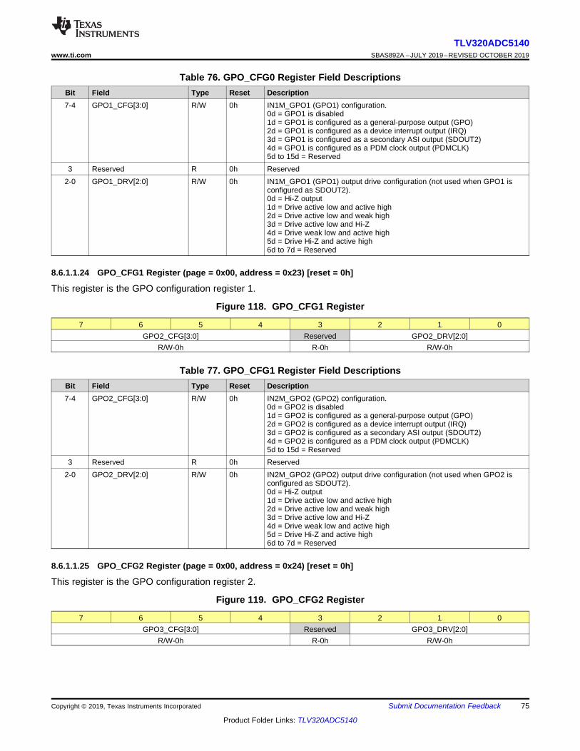
75
TLV320ADC5140www.ti.com SBAS892A –JULY 2019–REVISED OCTOBER 2019
Product Folder Links: TLV320ADC5140
Submit Documentation FeedbackCopyright © 2019, Texas Instruments Incorporated
Table 76. GPO_CFG0 Register Field DescriptionsBit Field Type Reset Description7-4 GPO1_CFG[3:0] R/W 0h IN1M_GPO1 (GPO1) configuration.
0d = GPO1 is disabled1d = GPO1 is configured as a general-purpose output (GPO)2d = GPO1 is configured as a device interrupt output (IRQ)3d = GPO1 is configured as a secondary ASI output (SDOUT2)4d = GPO1 is configured as a PDM clock output (PDMCLK)5d to 15d = Reserved
3 Reserved R 0h Reserved2-0 GPO1_DRV[2:0] R/W 0h IN1M_GPO1 (GPO1) output drive configuration (not used when GPO1 is
configured as SDOUT2).0d = Hi-Z output1d = Drive active low and active high2d = Drive active low and weak high3d = Drive active low and Hi-Z4d = Drive weak low and active high5d = Drive Hi-Z and active high6d to 7d = Reserved
8.6.1.1.24 GPO_CFG1 Register (page = 0x00, address = 0x23) [reset = 0h]
This register is the GPO configuration register 1.
Figure 118. GPO_CFG1 Register
7 6 5 4 3 2 1 0GPO2_CFG[3:0] Reserved GPO2_DRV[2:0]
R/W-0h R-0h R/W-0h
Table 77. GPO_CFG1 Register Field DescriptionsBit Field Type Reset Description7-4 GPO2_CFG[3:0] R/W 0h IN2M_GPO2 (GPO2) configuration.
0d = GPO2 is disabled1d = GPO2 is configured as a general-purpose output (GPO)2d = GPO2 is configured as a device interrupt output (IRQ)3d = GPO2 is configured as a secondary ASI output (SDOUT2)4d = GPO2 is configured as a PDM clock output (PDMCLK)5d to 15d = Reserved
3 Reserved R 0h Reserved2-0 GPO2_DRV[2:0] R/W 0h IN2M_GPO2 (GPO2) output drive configuration (not used when GPO2 is
configured as SDOUT2).0d = Hi-Z output1d = Drive active low and active high2d = Drive active low and weak high3d = Drive active low and Hi-Z4d = Drive weak low and active high5d = Drive Hi-Z and active high6d to 7d = Reserved
8.6.1.1.25 GPO_CFG2 Register (page = 0x00, address = 0x24) [reset = 0h]
This register is the GPO configuration register 2.
Figure 119. GPO_CFG2 Register
7 6 5 4 3 2 1 0GPO3_CFG[3:0] Reserved GPO3_DRV[2:0]
R/W-0h R-0h R/W-0h
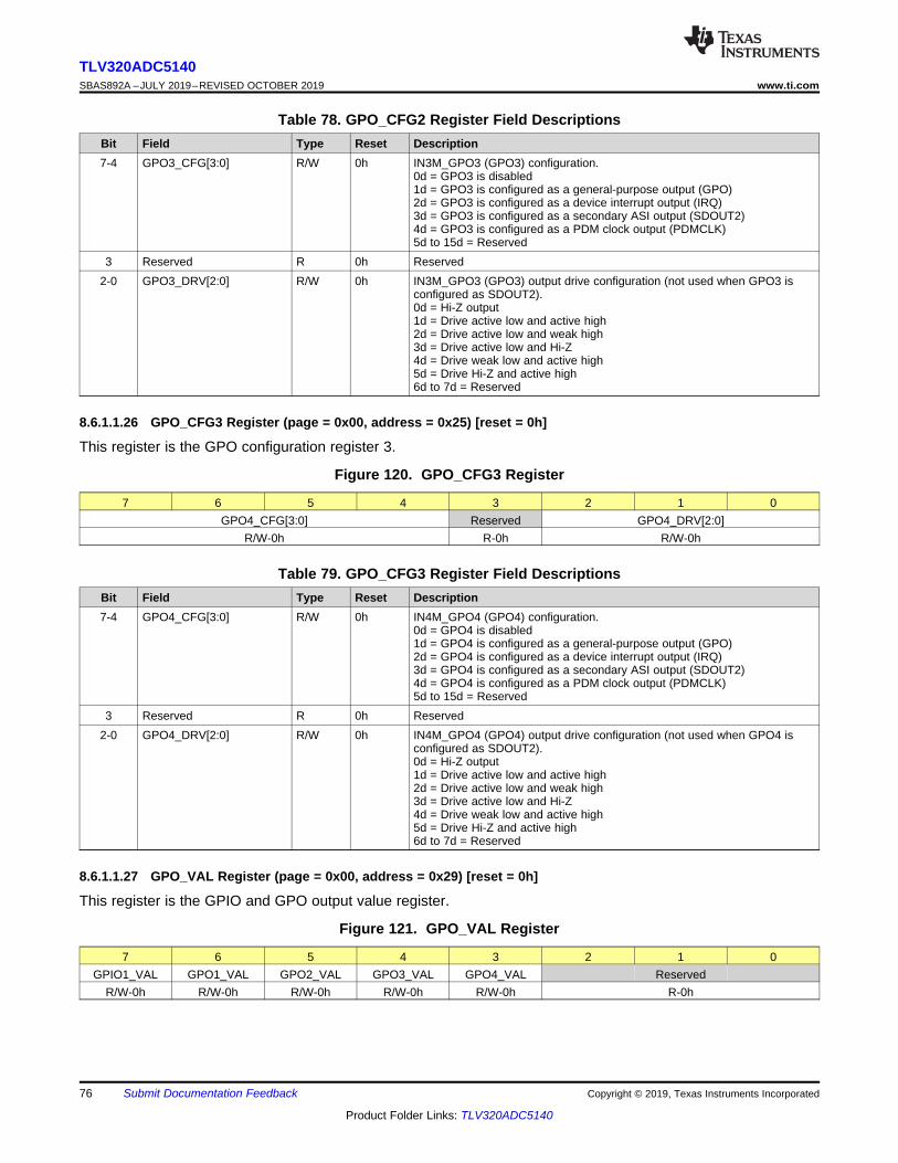
76
TLV320ADC5140SBAS892A –JULY 2019–REVISED OCTOBER 2019 www.ti.com
Product Folder Links: TLV320ADC5140
Submit Documentation Feedback Copyright © 2019, Texas Instruments Incorporated
Table 78. GPO_CFG2 Register Field DescriptionsBit Field Type Reset Description7-4 GPO3_CFG[3:0] R/W 0h IN3M_GPO3 (GPO3) configuration.
0d = GPO3 is disabled1d = GPO3 is configured as a general-purpose output (GPO)2d = GPO3 is configured as a device interrupt output (IRQ)3d = GPO3 is configured as a secondary ASI output (SDOUT2)4d = GPO3 is configured as a PDM clock output (PDMCLK)5d to 15d = Reserved
3 Reserved R 0h Reserved2-0 GPO3_DRV[2:0] R/W 0h IN3M_GPO3 (GPO3) output drive configuration (not used when GPO3 is
configured as SDOUT2).0d = Hi-Z output1d = Drive active low and active high2d = Drive active low and weak high3d = Drive active low and Hi-Z4d = Drive weak low and active high5d = Drive Hi-Z and active high6d to 7d = Reserved
8.6.1.1.26 GPO_CFG3 Register (page = 0x00, address = 0x25) [reset = 0h]
This register is the GPO configuration register 3.
Figure 120. GPO_CFG3 Register
7 6 5 4 3 2 1 0GPO4_CFG[3:0] Reserved GPO4_DRV[2:0]
R/W-0h R-0h R/W-0h
Table 79. GPO_CFG3 Register Field DescriptionsBit Field Type Reset Description7-4 GPO4_CFG[3:0] R/W 0h IN4M_GPO4 (GPO4) configuration.
0d = GPO4 is disabled1d = GPO4 is configured as a general-purpose output (GPO)2d = GPO4 is configured as a device interrupt output (IRQ)3d = GPO4 is configured as a secondary ASI output (SDOUT2)4d = GPO4 is configured as a PDM clock output (PDMCLK)5d to 15d = Reserved
3 Reserved R 0h Reserved2-0 GPO4_DRV[2:0] R/W 0h IN4M_GPO4 (GPO4) output drive configuration (not used when GPO4 is
configured as SDOUT2).0d = Hi-Z output1d = Drive active low and active high2d = Drive active low and weak high3d = Drive active low and Hi-Z4d = Drive weak low and active high5d = Drive Hi-Z and active high6d to 7d = Reserved
8.6.1.1.27 GPO_VAL Register (page = 0x00, address = 0x29) [reset = 0h]
This register is the GPIO and GPO output value register.
Figure 121. GPO_VAL Register
7 6 5 4 3 2 1 0GPIO1_VAL GPO1_VAL GPO2_VAL GPO3_VAL GPO4_VAL Reserved
R/W-0h R/W-0h R/W-0h R/W-0h R/W-0h R-0h
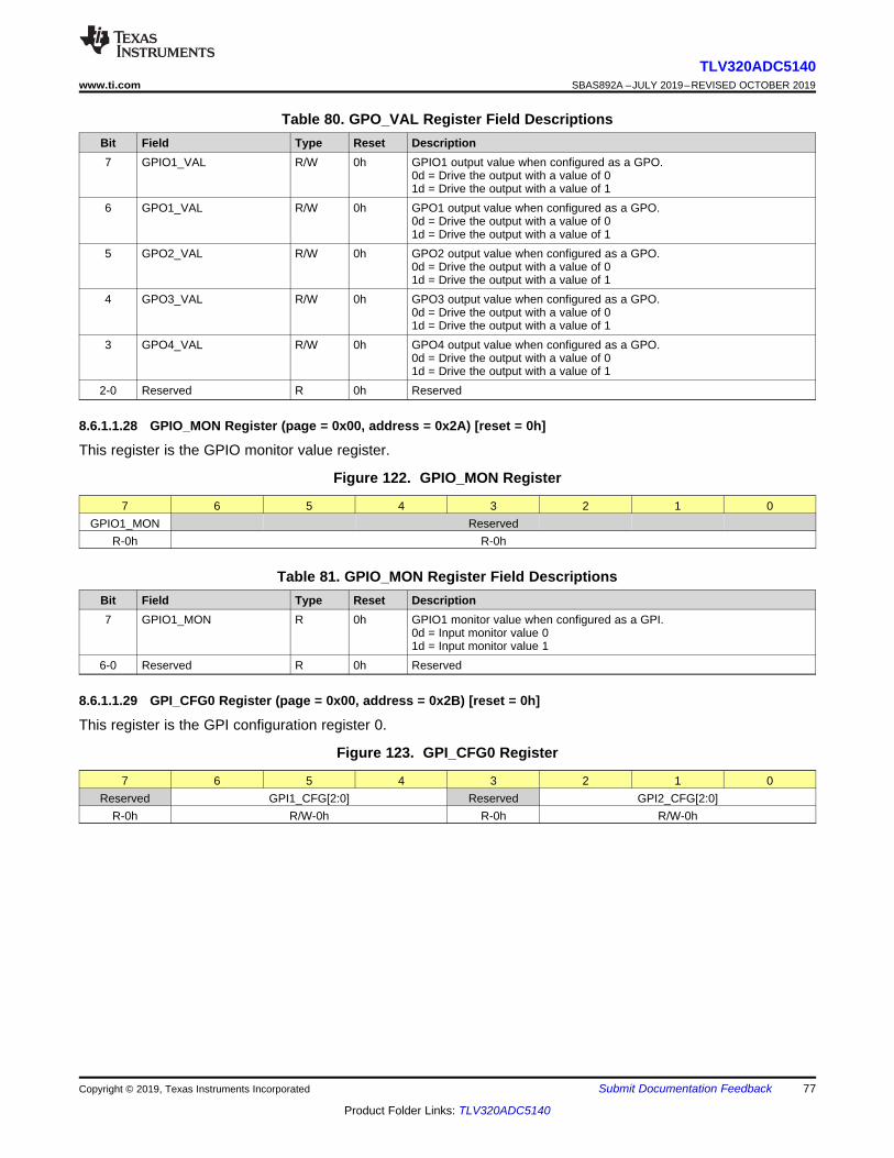
77
TLV320ADC5140www.ti.com SBAS892A –JULY 2019–REVISED OCTOBER 2019
Product Folder Links: TLV320ADC5140
Submit Documentation FeedbackCopyright © 2019, Texas Instruments Incorporated
Table 80. GPO_VAL Register Field DescriptionsBit Field Type Reset Description7 GPIO1_VAL R/W 0h GPIO1 output value when configured as a GPO.
0d = Drive the output with a value of 01d = Drive the output with a value of 1
6 GPO1_VAL R/W 0h GPO1 output value when configured as a GPO.0d = Drive the output with a value of 01d = Drive the output with a value of 1
5 GPO2_VAL R/W 0h GPO2 output value when configured as a GPO.0d = Drive the output with a value of 01d = Drive the output with a value of 1
4 GPO3_VAL R/W 0h GPO3 output value when configured as a GPO.0d = Drive the output with a value of 01d = Drive the output with a value of 1
3 GPO4_VAL R/W 0h GPO4 output value when configured as a GPO.0d = Drive the output with a value of 01d = Drive the output with a value of 1
2-0 Reserved R 0h Reserved
8.6.1.1.28 GPIO_MON Register (page = 0x00, address = 0x2A) [reset = 0h]
This register is the GPIO monitor value register.
Figure 122. GPIO_MON Register
7 6 5 4 3 2 1 0GPIO1_MON Reserved
R-0h R-0h
Table 81. GPIO_MON Register Field DescriptionsBit Field Type Reset Description7 GPIO1_MON R 0h GPIO1 monitor value when configured as a GPI.
0d = Input monitor value 01d = Input monitor value 1
6-0 Reserved R 0h Reserved
8.6.1.1.29 GPI_CFG0 Register (page = 0x00, address = 0x2B) [reset = 0h]
This register is the GPI configuration register 0.
Figure 123. GPI_CFG0 Register
7 6 5 4 3 2 1 0Reserved GPI1_CFG[2:0] Reserved GPI2_CFG[2:0]
R-0h R/W-0h R-0h R/W-0h
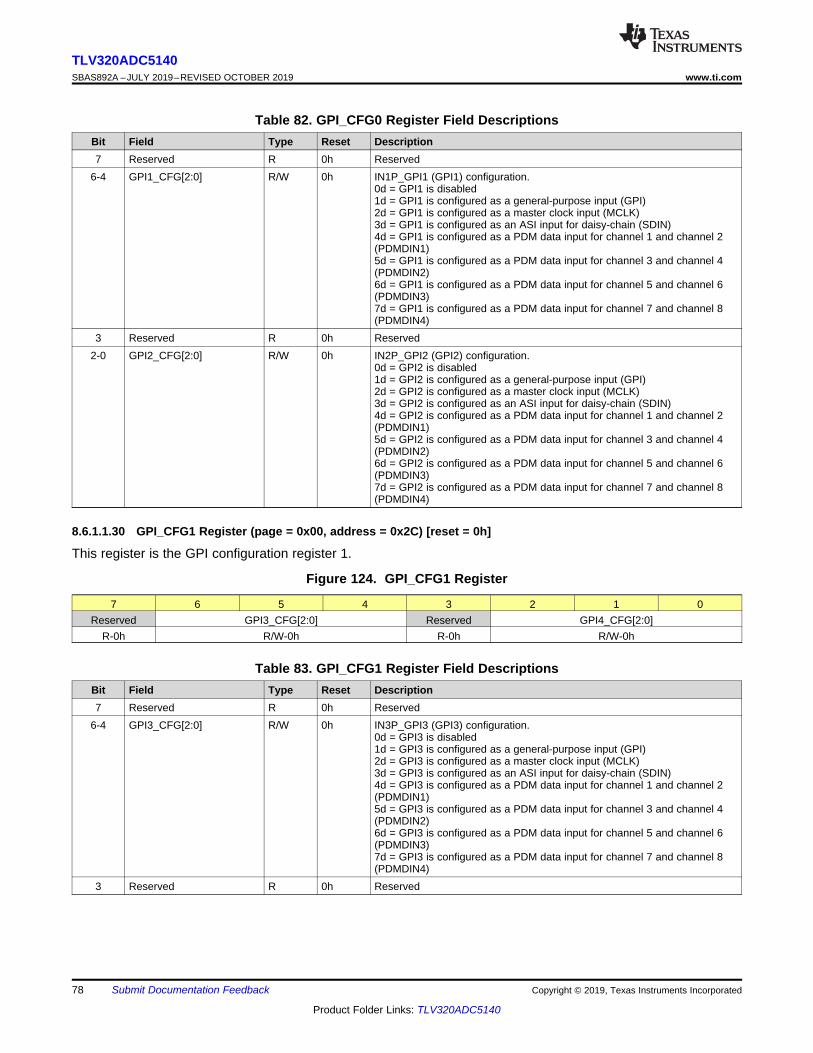
78
TLV320ADC5140SBAS892A –JULY 2019–REVISED OCTOBER 2019 www.ti.com
Product Folder Links: TLV320ADC5140
Submit Documentation Feedback Copyright © 2019, Texas Instruments Incorporated
Table 82. GPI_CFG0 Register Field DescriptionsBit Field Type Reset Description7 Reserved R 0h Reserved
6-4 GPI1_CFG[2:0] R/W 0h IN1P_GPI1 (GPI1) configuration.0d = GPI1 is disabled1d = GPI1 is configured as a general-purpose input (GPI)2d = GPI1 is configured as a master clock input (MCLK)3d = GPI1 is configured as an ASI input for daisy-chain (SDIN)4d = GPI1 is configured as a PDM data input for channel 1 and channel 2(PDMDIN1)5d = GPI1 is configured as a PDM data input for channel 3 and channel 4(PDMDIN2)6d = GPI1 is configured as a PDM data input for channel 5 and channel 6(PDMDIN3)7d = GPI1 is configured as a PDM data input for channel 7 and channel 8(PDMDIN4)
3 Reserved R 0h Reserved2-0 GPI2_CFG[2:0] R/W 0h IN2P_GPI2 (GPI2) configuration.
0d = GPI2 is disabled1d = GPI2 is configured as a general-purpose input (GPI)2d = GPI2 is configured as a master clock input (MCLK)3d = GPI2 is configured as an ASI input for daisy-chain (SDIN)4d = GPI2 is configured as a PDM data input for channel 1 and channel 2(PDMDIN1)5d = GPI2 is configured as a PDM data input for channel 3 and channel 4(PDMDIN2)6d = GPI2 is configured as a PDM data input for channel 5 and channel 6(PDMDIN3)7d = GPI2 is configured as a PDM data input for channel 7 and channel 8(PDMDIN4)
8.6.1.1.30 GPI_CFG1 Register (page = 0x00, address = 0x2C) [reset = 0h]
This register is the GPI configuration register 1.
Figure 124. GPI_CFG1 Register
7 6 5 4 3 2 1 0Reserved GPI3_CFG[2:0] Reserved GPI4_CFG[2:0]
R-0h R/W-0h R-0h R/W-0h
Table 83. GPI_CFG1 Register Field DescriptionsBit Field Type Reset Description7 Reserved R 0h Reserved
6-4 GPI3_CFG[2:0] R/W 0h IN3P_GPI3 (GPI3) configuration.0d = GPI3 is disabled1d = GPI3 is configured as a general-purpose input (GPI)2d = GPI3 is configured as a master clock input (MCLK)3d = GPI3 is configured as an ASI input for daisy-chain (SDIN)4d = GPI3 is configured as a PDM data input for channel 1 and channel 2(PDMDIN1)5d = GPI3 is configured as a PDM data input for channel 3 and channel 4(PDMDIN2)6d = GPI3 is configured as a PDM data input for channel 5 and channel 6(PDMDIN3)7d = GPI3 is configured as a PDM data input for channel 7 and channel 8(PDMDIN4)
3 Reserved R 0h Reserved
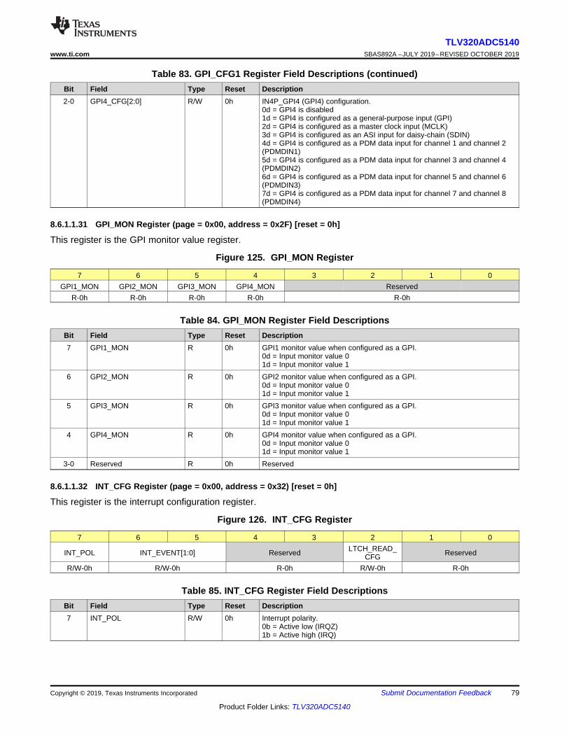
79
TLV320ADC5140www.ti.com SBAS892A –JULY 2019–REVISED OCTOBER 2019
Product Folder Links: TLV320ADC5140
Submit Documentation FeedbackCopyright © 2019, Texas Instruments Incorporated
Table 83. GPI_CFG1 Register Field Descriptions (continued)Bit Field Type Reset Description2-0 GPI4_CFG[2:0] R/W 0h IN4P_GPI4 (GPI4) configuration.
0d = GPI4 is disabled1d = GPI4 is configured as a general-purpose input (GPI)2d = GPI4 is configured as a master clock input (MCLK)3d = GPI4 is configured as an ASI input for daisy-chain (SDIN)4d = GPI4 is configured as a PDM data input for channel 1 and channel 2(PDMDIN1)5d = GPI4 is configured as a PDM data input for channel 3 and channel 4(PDMDIN2)6d = GPI4 is configured as a PDM data input for channel 5 and channel 6(PDMDIN3)7d = GPI4 is configured as a PDM data input for channel 7 and channel 8(PDMDIN4)
8.6.1.1.31 GPI_MON Register (page = 0x00, address = 0x2F) [reset = 0h]
This register is the GPI monitor value register.
Figure 125. GPI_MON Register
7 6 5 4 3 2 1 0GPI1_MON GPI2_MON GPI3_MON GPI4_MON Reserved
R-0h R-0h R-0h R-0h R-0h
Table 84. GPI_MON Register Field DescriptionsBit Field Type Reset Description7 GPI1_MON R 0h GPI1 monitor value when configured as a GPI.
0d = Input monitor value 01d = Input monitor value 1
6 GPI2_MON R 0h GPI2 monitor value when configured as a GPI.0d = Input monitor value 01d = Input monitor value 1
5 GPI3_MON R 0h GPI3 monitor value when configured as a GPI.0d = Input monitor value 01d = Input monitor value 1
4 GPI4_MON R 0h GPI4 monitor value when configured as a GPI.0d = Input monitor value 01d = Input monitor value 1
3-0 Reserved R 0h Reserved
8.6.1.1.32 INT_CFG Register (page = 0x00, address = 0x32) [reset = 0h]
This register is the interrupt configuration register.
Figure 126. INT_CFG Register
7 6 5 4 3 2 1 0
INT_POL INT_EVENT[1:0] Reserved LTCH_READ_CFG Reserved
R/W-0h R/W-0h R-0h R/W-0h R-0h
Table 85. INT_CFG Register Field DescriptionsBit Field Type Reset Description7 INT_POL R/W 0h Interrupt polarity.
0b = Active low (IRQZ)1b = Active high (IRQ)
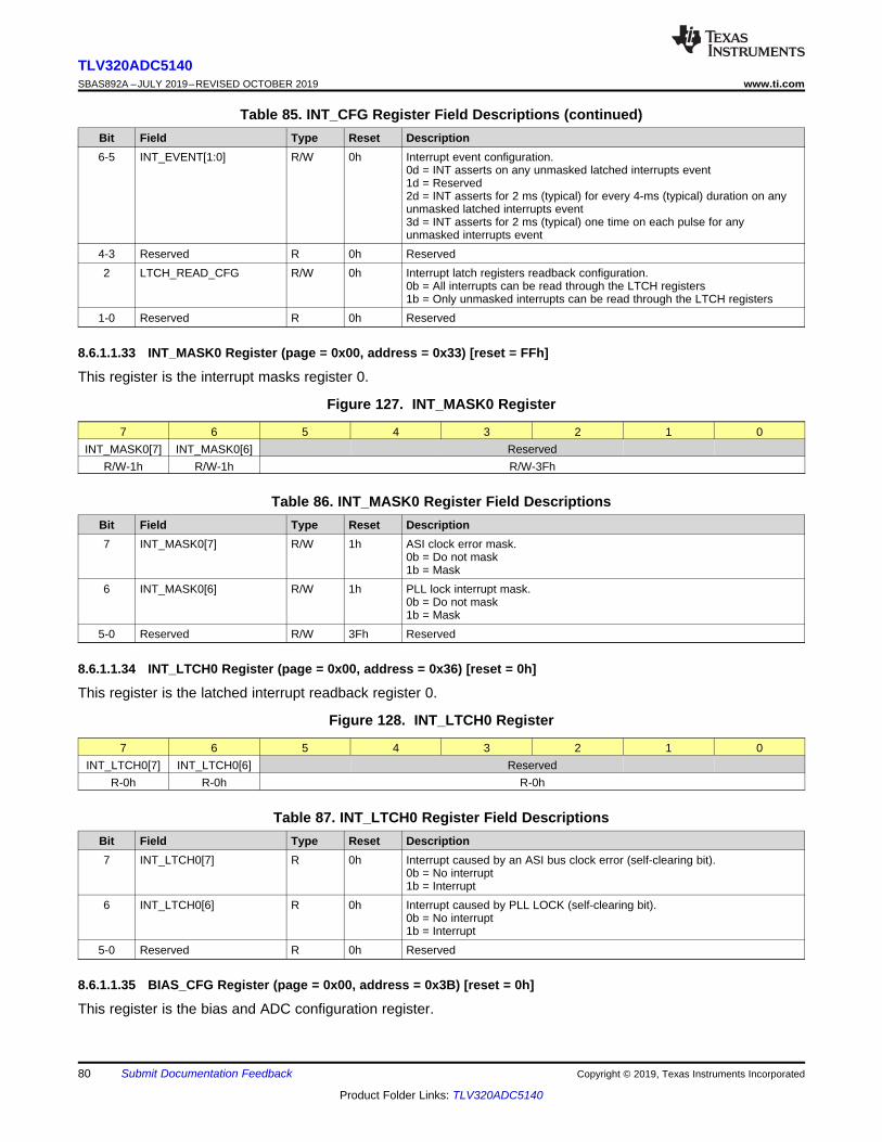
80
TLV320ADC5140SBAS892A –JULY 2019–REVISED OCTOBER 2019 www.ti.com
Product Folder Links: TLV320ADC5140
Submit Documentation Feedback Copyright © 2019, Texas Instruments Incorporated
Table 85. INT_CFG Register Field Descriptions (continued)Bit Field Type Reset Description6-5 INT_EVENT[1:0] R/W 0h Interrupt event configuration.
0d = INT asserts on any unmasked latched interrupts event1d = Reserved2d = INT asserts for 2 ms (typical) for every 4-ms (typical) duration on anyunmasked latched interrupts event3d = INT asserts for 2 ms (typical) one time on each pulse for anyunmasked interrupts event
4-3 Reserved R 0h Reserved2 LTCH_READ_CFG R/W 0h Interrupt latch registers readback configuration.
0b = All interrupts can be read through the LTCH registers1b = Only unmasked interrupts can be read through the LTCH registers
1-0 Reserved R 0h Reserved
8.6.1.1.33 INT_MASK0 Register (page = 0x00, address = 0x33) [reset = FFh]
This register is the interrupt masks register 0.
Figure 127. INT_MASK0 Register
7 6 5 4 3 2 1 0INT_MASK0[7] INT_MASK0[6] Reserved
R/W-1h R/W-1h R/W-3Fh
Table 86. INT_MASK0 Register Field DescriptionsBit Field Type Reset Description7 INT_MASK0[7] R/W 1h ASI clock error mask.
0b = Do not mask1b = Mask
6 INT_MASK0[6] R/W 1h PLL lock interrupt mask.0b = Do not mask1b = Mask
5-0 Reserved R/W 3Fh Reserved
8.6.1.1.34 INT_LTCH0 Register (page = 0x00, address = 0x36) [reset = 0h]
This register is the latched interrupt readback register 0.
Figure 128. INT_LTCH0 Register
7 6 5 4 3 2 1 0INT_LTCH0[7] INT_LTCH0[6] Reserved
R-0h R-0h R-0h
Table 87. INT_LTCH0 Register Field DescriptionsBit Field Type Reset Description7 INT_LTCH0[7] R 0h Interrupt caused by an ASI bus clock error (self-clearing bit).
0b = No interrupt1b = Interrupt
6 INT_LTCH0[6] R 0h Interrupt caused by PLL LOCK (self-clearing bit).0b = No interrupt1b = Interrupt
5-0 Reserved R 0h Reserved
8.6.1.1.35 BIAS_CFG Register (page = 0x00, address = 0x3B) [reset = 0h]
This register is the bias and ADC configuration register.
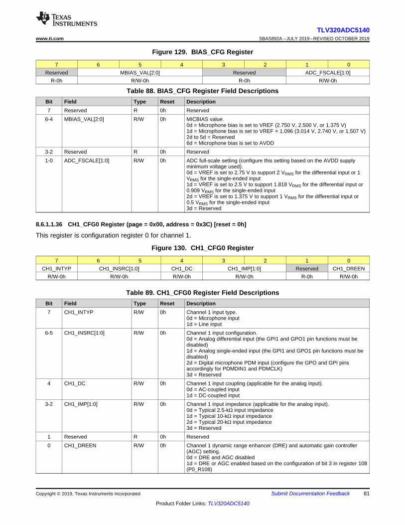
81
TLV320ADC5140www.ti.com SBAS892A –JULY 2019–REVISED OCTOBER 2019
Product Folder Links: TLV320ADC5140
Submit Documentation FeedbackCopyright © 2019, Texas Instruments Incorporated
Figure 129. BIAS_CFG Register
7 6 5 4 3 2 1 0Reserved MBIAS_VAL[2:0] Reserved ADC_FSCALE[1:0]
R-0h R/W-0h R-0h R/W-0h
Table 88. BIAS_CFG Register Field DescriptionsBit Field Type Reset Description7 Reserved R 0h Reserved
6-4 MBIAS_VAL[2:0] R/W 0h MICBIAS value.0d = Microphone bias is set to VREF (2.750 V, 2.500 V, or 1.375 V)1d = Microphone bias is set to VREF × 1.096 (3.014 V, 2.740 V, or 1.507 V)2d to 5d = Reserved6d = Microphone bias is set to AVDD
3-2 Reserved R 0h Reserved1-0 ADC_FSCALE[1:0] R/W 0h ADC full-scale setting (configure this setting based on the AVDD supply
minimum voltage used).0d = VREF is set to 2.75 V to support 2 VRMS for the differential input or 1VRMS for the single-ended input1d = VREF is set to 2.5 V to support 1.818 VRMS for the differential input or0.909 VRMS for the single-ended input2d = VREF is set to 1.375 V to support 1 VRMS for the differential input or0.5 VRMS for the single-ended input3d = Reserved
8.6.1.1.36 CH1_CFG0 Register (page = 0x00, address = 0x3C) [reset = 0h]
This register is configuration register 0 for channel 1.
Figure 130. CH1_CFG0 Register
7 6 5 4 3 2 1 0CH1_INTYP CH1_INSRC[1:0] CH1_DC CH1_IMP[1:0] Reserved CH1_DREEN
R/W-0h R/W-0h R/W-0h R/W-0h R-0h R/W-0h
Table 89. CH1_CFG0 Register Field DescriptionsBit Field Type Reset Description7 CH1_INTYP R/W 0h Channel 1 input type.
0d = Microphone input1d = Line input
6-5 CH1_INSRC[1:0] R/W 0h Channel 1 input configuration.0d = Analog differential input (the GPI1 and GPO1 pin functions must bedisabled)1d = Analog single-ended input (the GPI1 and GPO1 pin functions must bedisabled)2d = Digital microphone PDM input (configure the GPO and GPI pinsaccordingly for PDMDIN1 and PDMCLK)3d = Reserved
4 CH1_DC R/W 0h Channel 1 input coupling (applicable for the analog input).0d = AC-coupled input1d = DC-coupled input
3-2 CH1_IMP[1:0] R/W 0h Channel 1 input impedance (applicable for the analog input).0d = Typical 2.5-kΩ input impedance1d = Typical 10-kΩ input impedance2d = Typical 20-kΩ input impedance3d = Reserved
1 Reserved R 0h Reserved0 CH1_DREEN R/W 0h Channel 1 dynamic range enhancer (DRE) and automatic gain controller
(AGC) setting.0d = DRE and AGC disabled1d = DRE or AGC enabled based on the configuration of bit 3 in register 108(P0_R108)
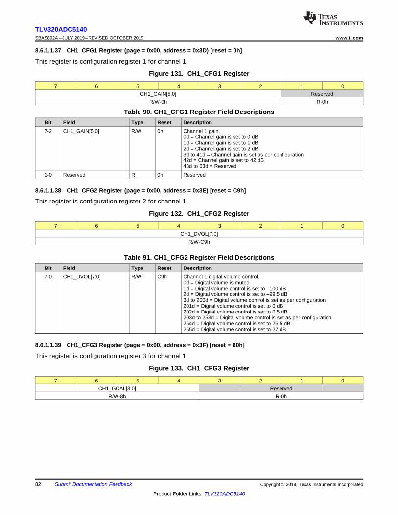
82
TLV320ADC5140SBAS892A –JULY 2019–REVISED OCTOBER 2019 www.ti.com
Product Folder Links: TLV320ADC5140
Submit Documentation Feedback Copyright © 2019, Texas Instruments Incorporated
8.6.1.1.37 CH1_CFG1 Register (page = 0x00, address = 0x3D) [reset = 0h]
This register is configuration register 1 for channel 1.
Figure 131. CH1_CFG1 Register
7 6 5 4 3 2 1 0CH1_GAIN[5:0] Reserved
R/W-0h R-0h
Table 90. CH1_CFG1 Register Field DescriptionsBit Field Type Reset Description7-2 CH1_GAIN[5:0] R/W 0h Channel 1 gain.
0d = Channel gain is set to 0 dB1d = Channel gain is set to 1 dB2d = Channel gain is set to 2 dB3d to 41d = Channel gain is set as per configuration42d = Channel gain is set to 42 dB43d to 63d = Reserved
1-0 Reserved R 0h Reserved
8.6.1.1.38 CH1_CFG2 Register (page = 0x00, address = 0x3E) [reset = C9h]
This register is configuration register 2 for channel 1.
Figure 132. CH1_CFG2 Register
7 6 5 4 3 2 1 0CH1_DVOL[7:0]
R/W-C9h
Table 91. CH1_CFG2 Register Field DescriptionsBit Field Type Reset Description7-0 CH1_DVOL[7:0] R/W C9h Channel 1 digital volume control.
0d = Digital volume is muted1d = Digital volume control is set to –100 dB2d = Digital volume control is set to –99.5 dB3d to 200d = Digital volume control is set as per configuration201d = Digital volume control is set to 0 dB202d = Digital volume control is set to 0.5 dB203d to 253d = Digital volume control is set as per configuration254d = Digital volume control is set to 26.5 dB255d = Digital volume control is set to 27 dB
8.6.1.1.39 CH1_CFG3 Register (page = 0x00, address = 0x3F) [reset = 80h]
This register is configuration register 3 for channel 1.
Figure 133. CH1_CFG3 Register
7 6 5 4 3 2 1 0CH1_GCAL[3:0] Reserved
R/W-8h R-0h
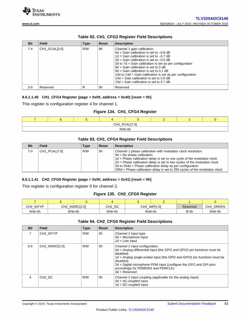
83
TLV320ADC5140www.ti.com SBAS892A –JULY 2019–REVISED OCTOBER 2019
Product Folder Links: TLV320ADC5140
Submit Documentation FeedbackCopyright © 2019, Texas Instruments Incorporated
Table 92. CH1_CFG3 Register Field DescriptionsBit Field Type Reset Description7-4 CH1_GCAL[3:0] R/W 8h Channel 1 gain calibration.
0d = Gain calibration is set to –0.8 dB1d = Gain calibration is set to –0.7 dB2d = Gain calibration is set to –0.6 dB3d to 7d = Gain calibration is set as per configuration8d = Gain calibration is set to 0 dB9d = Gain calibration is set to 0.1 dB10d to 13d = Gain calibration is set as per configuration14d = Gain calibration is set to 0.6 dB15d = Gain calibration is set to 0.7 dB
3-0 Reserved R 0h Reserved
8.6.1.1.40 CH1_CFG4 Register (page = 0x00, address = 0x40) [reset = 0h]
This register is configuration register 4 for channel 1.
Figure 134. CH1_CFG4 Register
7 6 5 4 3 2 1 0CH1_PCAL[7:0]
R/W-0h
Table 93. CH1_CFG4 Register Field DescriptionsBit Field Type Reset Description7-0 CH1_PCAL[7:0] R/W 0h Channel 1 phase calibration with modulator clock resolution.
0d = No phase calibration1d = Phase calibration delay is set to one cycle of the modulator clock2d = Phase calibration delay is set to two cycles of the modulator clock3d to 254d = Phase calibration delay as per configuration255d = Phase calibration delay is set to 255 cycles of the modulator clock
8.6.1.1.41 CH2_CFG0 Register (page = 0x00, address = 0x41) [reset = 0h]
This register is configuration register 0 for channel 2.
Figure 135. CH2_CFG0 Register
7 6 5 4 3 2 1 0CH2_INTYP CH2_INSRC[1:0] CH2_DC CH2_IMP[1:0] Reserved CH2_DREEN
R/W-0h R/W-0h R/W-0h R/W-0h R-0h R/W-0h
Table 94. CH2_CFG0 Register Field DescriptionsBit Field Type Reset Description7 CH2_INTYP R/W 0h Channel 2 input type.
0d = Microphone input1d = Line input
6-5 CH2_INSRC[1:0] R/W 0h Channel 2 input configuration.0d = Analog differential input (the GPI2 and GPO2 pin functions must bedisabled)1d = Analog single-ended input (the GPI2 and GPO2 pin functions must bedisabled)2d = Digital microphone PDM input (configure the GPO and GPI pinsaccordingly for PDMDIN1 and PDMCLK)3d = Reserved
4 CH2_DC R/W 0h Channel 2 input coupling (applicable for the analog input).0d = AC-coupled input1d = DC-coupled input
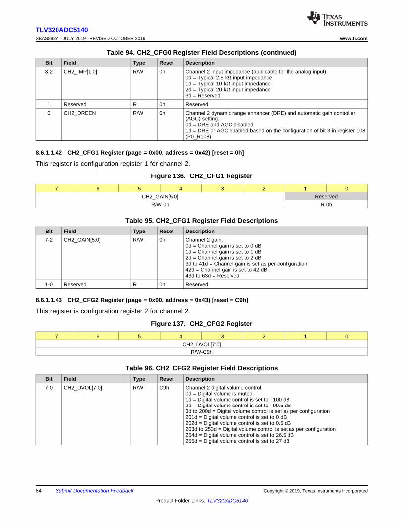
84
TLV320ADC5140SBAS892A –JULY 2019–REVISED OCTOBER 2019 www.ti.com
Product Folder Links: TLV320ADC5140
Submit Documentation Feedback Copyright © 2019, Texas Instruments Incorporated
Table 94. CH2_CFG0 Register Field Descriptions (continued)Bit Field Type Reset Description3-2 CH2_IMP[1:0] R/W 0h Channel 2 input impedance (applicable for the analog input).
0d = Typical 2.5-kΩ input impedance1d = Typical 10-kΩ input impedance2d = Typical 20-kΩ input impedance3d = Reserved
1 Reserved R 0h Reserved0 CH2_DREEN R/W 0h Channel 2 dynamic range enhancer (DRE) and automatic gain controller
(AGC) setting.0d = DRE and AGC disabled1d = DRE or AGC enabled based on the configuration of bit 3 in register 108(P0_R108)
8.6.1.1.42 CH2_CFG1 Register (page = 0x00, address = 0x42) [reset = 0h]
This register is configuration register 1 for channel 2.
Figure 136. CH2_CFG1 Register
7 6 5 4 3 2 1 0CH2_GAIN[5:0] Reserved
R/W-0h R-0h
Table 95. CH2_CFG1 Register Field DescriptionsBit Field Type Reset Description7-2 CH2_GAIN[5:0] R/W 0h Channel 2 gain.
0d = Channel gain is set to 0 dB1d = Channel gain is set to 1 dB2d = Channel gain is set to 2 dB3d to 41d = Channel gain is set as per configuration42d = Channel gain is set to 42 dB43d to 63d = Reserved
1-0 Reserved R 0h Reserved
8.6.1.1.43 CH2_CFG2 Register (page = 0x00, address = 0x43) [reset = C9h]
This register is configuration register 2 for channel 2.
Figure 137. CH2_CFG2 Register
7 6 5 4 3 2 1 0CH2_DVOL[7:0]
R/W-C9h
Table 96. CH2_CFG2 Register Field DescriptionsBit Field Type Reset Description7-0 CH2_DVOL[7:0] R/W C9h Channel 2 digital volume control.
0d = Digital volume is muted1d = Digital volume control is set to –100 dB2d = Digital volume control is set to –99.5 dB3d to 200d = Digital volume control is set as per configuration201d = Digital volume control is set to 0 dB202d = Digital volume control is set to 0.5 dB203d to 253d = Digital volume control is set as per configuration254d = Digital volume control is set to 26.5 dB255d = Digital volume control is set to 27 dB
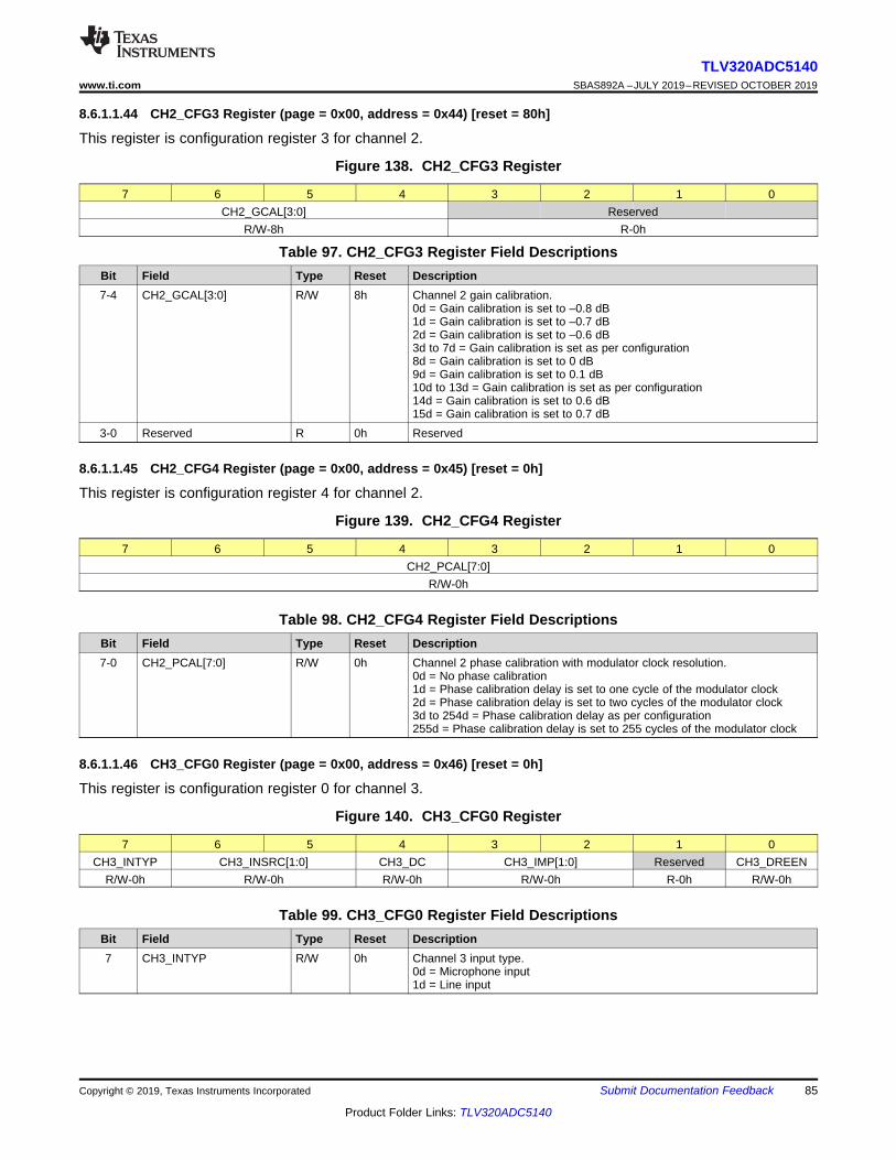
85
TLV320ADC5140www.ti.com SBAS892A –JULY 2019–REVISED OCTOBER 2019
Product Folder Links: TLV320ADC5140
Submit Documentation FeedbackCopyright © 2019, Texas Instruments Incorporated
8.6.1.1.44 CH2_CFG3 Register (page = 0x00, address = 0x44) [reset = 80h]
This register is configuration register 3 for channel 2.
Figure 138. CH2_CFG3 Register
7 6 5 4 3 2 1 0CH2_GCAL[3:0] Reserved
R/W-8h R-0h
Table 97. CH2_CFG3 Register Field DescriptionsBit Field Type Reset Description7-4 CH2_GCAL[3:0] R/W 8h Channel 2 gain calibration.
0d = Gain calibration is set to –0.8 dB1d = Gain calibration is set to –0.7 dB2d = Gain calibration is set to –0.6 dB3d to 7d = Gain calibration is set as per configuration8d = Gain calibration is set to 0 dB9d = Gain calibration is set to 0.1 dB10d to 13d = Gain calibration is set as per configuration14d = Gain calibration is set to 0.6 dB15d = Gain calibration is set to 0.7 dB
3-0 Reserved R 0h Reserved
8.6.1.1.45 CH2_CFG4 Register (page = 0x00, address = 0x45) [reset = 0h]
This register is configuration register 4 for channel 2.
Figure 139. CH2_CFG4 Register
7 6 5 4 3 2 1 0CH2_PCAL[7:0]
R/W-0h
Table 98. CH2_CFG4 Register Field DescriptionsBit Field Type Reset Description7-0 CH2_PCAL[7:0] R/W 0h Channel 2 phase calibration with modulator clock resolution.
0d = No phase calibration1d = Phase calibration delay is set to one cycle of the modulator clock2d = Phase calibration delay is set to two cycles of the modulator clock3d to 254d = Phase calibration delay as per configuration255d = Phase calibration delay is set to 255 cycles of the modulator clock
8.6.1.1.46 CH3_CFG0 Register (page = 0x00, address = 0x46) [reset = 0h]
This register is configuration register 0 for channel 3.
Figure 140. CH3_CFG0 Register
7 6 5 4 3 2 1 0CH3_INTYP CH3_INSRC[1:0] CH3_DC CH3_IMP[1:0] Reserved CH3_DREEN
R/W-0h R/W-0h R/W-0h R/W-0h R-0h R/W-0h
Table 99. CH3_CFG0 Register Field DescriptionsBit Field Type Reset Description7 CH3_INTYP R/W 0h Channel 3 input type.
0d = Microphone input1d = Line input
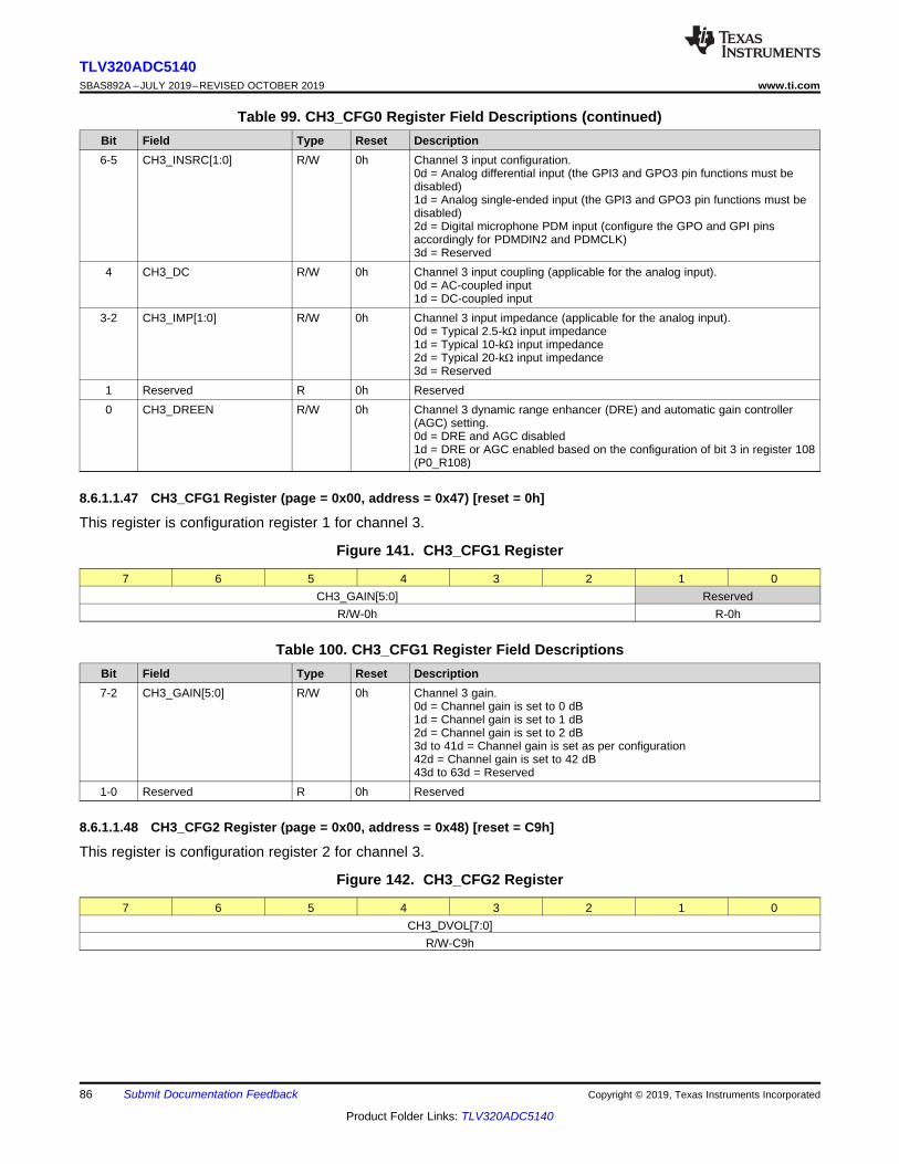
86
TLV320ADC5140SBAS892A –JULY 2019–REVISED OCTOBER 2019 www.ti.com
Product Folder Links: TLV320ADC5140
Submit Documentation Feedback Copyright © 2019, Texas Instruments Incorporated
Table 99. CH3_CFG0 Register Field Descriptions (continued)Bit Field Type Reset Description6-5 CH3_INSRC[1:0] R/W 0h Channel 3 input configuration.
0d = Analog differential input (the GPI3 and GPO3 pin functions must bedisabled)1d = Analog single-ended input (the GPI3 and GPO3 pin functions must bedisabled)2d = Digital microphone PDM input (configure the GPO and GPI pinsaccordingly for PDMDIN2 and PDMCLK)3d = Reserved
4 CH3_DC R/W 0h Channel 3 input coupling (applicable for the analog input).0d = AC-coupled input1d = DC-coupled input
3-2 CH3_IMP[1:0] R/W 0h Channel 3 input impedance (applicable for the analog input).0d = Typical 2.5-kΩ input impedance1d = Typical 10-kΩ input impedance2d = Typical 20-kΩ input impedance3d = Reserved
1 Reserved R 0h Reserved0 CH3_DREEN R/W 0h Channel 3 dynamic range enhancer (DRE) and automatic gain controller
(AGC) setting.0d = DRE and AGC disabled1d = DRE or AGC enabled based on the configuration of bit 3 in register 108(P0_R108)
8.6.1.1.47 CH3_CFG1 Register (page = 0x00, address = 0x47) [reset = 0h]
This register is configuration register 1 for channel 3.
Figure 141. CH3_CFG1 Register
7 6 5 4 3 2 1 0CH3_GAIN[5:0] Reserved
R/W-0h R-0h
Table 100. CH3_CFG1 Register Field DescriptionsBit Field Type Reset Description7-2 CH3_GAIN[5:0] R/W 0h Channel 3 gain.
0d = Channel gain is set to 0 dB1d = Channel gain is set to 1 dB2d = Channel gain is set to 2 dB3d to 41d = Channel gain is set as per configuration42d = Channel gain is set to 42 dB43d to 63d = Reserved
1-0 Reserved R 0h Reserved
8.6.1.1.48 CH3_CFG2 Register (page = 0x00, address = 0x48) [reset = C9h]
This register is configuration register 2 for channel 3.
Figure 142. CH3_CFG2 Register
7 6 5 4 3 2 1 0CH3_DVOL[7:0]
R/W-C9h
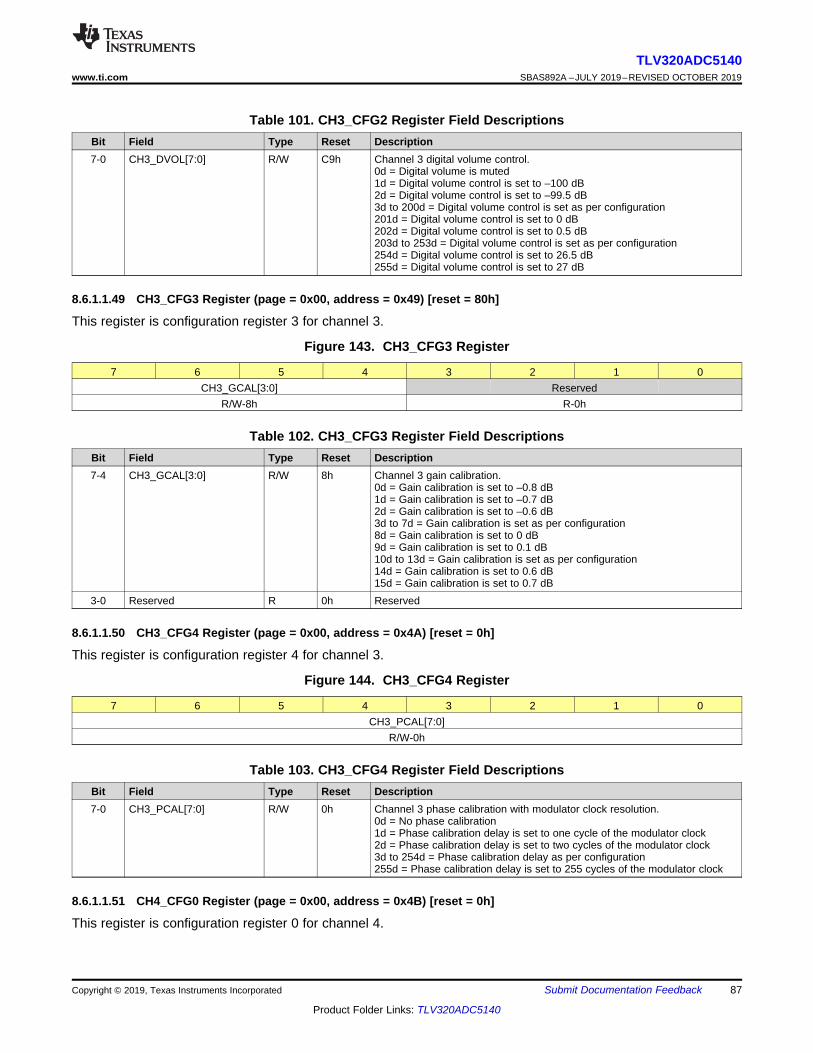
87
TLV320ADC5140www.ti.com SBAS892A –JULY 2019–REVISED OCTOBER 2019
Product Folder Links: TLV320ADC5140
Submit Documentation FeedbackCopyright © 2019, Texas Instruments Incorporated
Table 101. CH3_CFG2 Register Field DescriptionsBit Field Type Reset Description7-0 CH3_DVOL[7:0] R/W C9h Channel 3 digital volume control.
0d = Digital volume is muted1d = Digital volume control is set to –100 dB2d = Digital volume control is set to –99.5 dB3d to 200d = Digital volume control is set as per configuration201d = Digital volume control is set to 0 dB202d = Digital volume control is set to 0.5 dB203d to 253d = Digital volume control is set as per configuration254d = Digital volume control is set to 26.5 dB255d = Digital volume control is set to 27 dB
8.6.1.1.49 CH3_CFG3 Register (page = 0x00, address = 0x49) [reset = 80h]
This register is configuration register 3 for channel 3.
Figure 143. CH3_CFG3 Register
7 6 5 4 3 2 1 0CH3_GCAL[3:0] Reserved
R/W-8h R-0h
Table 102. CH3_CFG3 Register Field DescriptionsBit Field Type Reset Description7-4 CH3_GCAL[3:0] R/W 8h Channel 3 gain calibration.
0d = Gain calibration is set to –0.8 dB1d = Gain calibration is set to –0.7 dB2d = Gain calibration is set to –0.6 dB3d to 7d = Gain calibration is set as per configuration8d = Gain calibration is set to 0 dB9d = Gain calibration is set to 0.1 dB10d to 13d = Gain calibration is set as per configuration14d = Gain calibration is set to 0.6 dB15d = Gain calibration is set to 0.7 dB
3-0 Reserved R 0h Reserved
8.6.1.1.50 CH3_CFG4 Register (page = 0x00, address = 0x4A) [reset = 0h]
This register is configuration register 4 for channel 3.
Figure 144. CH3_CFG4 Register
7 6 5 4 3 2 1 0CH3_PCAL[7:0]
R/W-0h
Table 103. CH3_CFG4 Register Field DescriptionsBit Field Type Reset Description7-0 CH3_PCAL[7:0] R/W 0h Channel 3 phase calibration with modulator clock resolution.
0d = No phase calibration1d = Phase calibration delay is set to one cycle of the modulator clock2d = Phase calibration delay is set to two cycles of the modulator clock3d to 254d = Phase calibration delay as per configuration255d = Phase calibration delay is set to 255 cycles of the modulator clock
8.6.1.1.51 CH4_CFG0 Register (page = 0x00, address = 0x4B) [reset = 0h]
This register is configuration register 0 for channel 4.
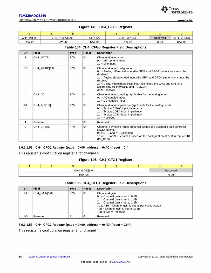
88
TLV320ADC5140SBAS892A –JULY 2019–REVISED OCTOBER 2019 www.ti.com
Product Folder Links: TLV320ADC5140
Submit Documentation Feedback Copyright © 2019, Texas Instruments Incorporated
Figure 145. CH4_CFG0 Register
7 6 5 4 3 2 1 0CH4_INTYP CH4_INSRC[1:0] CH4_DC CH4_IMP[1:0] Reserved CH4_DREEN
R/W-0h R/W-0h R/W-0h R/W-0h R-0h R/W-0h
Table 104. CH4_CFG0 Register Field DescriptionsBit Field Type Reset Description7 CH4_INTYP R/W 0h Channel 4 input type.
0d = Microphone input1d = Line input
6-5 CH4_INSRC[1:0] R/W 0h Channel 4 input configuration.0d = Analog differential input (the GPI4 and GPO4 pin functions must bedisabled)1d = Analog single-ended input (the GPI4 and GPO4 pin functions must bedisabled)2d = Digital microphone PDM input (configure the GPO and GPI pinsaccordingly for PDMDIN2 and PDMCLK)3d = Reserved
4 CH4_DC R/W 0h Channel 4 input coupling (applicable for the analog input).0d = AC-coupled input1d = DC-coupled input
3-2 CH4_IMP[1:0] R/W 0h Channel 4 input impedance (applicable for the analog input).0d = Typical 2.5-kΩ input impedance1d = Typical 10-kΩ input impedance2d = Typical 20-kΩ input impedance3d = Reserved
1 Reserved R 0h Reserved0 CH4_DREEN R/W 0h Channel 4 dynamic range enhancer (DRE) and automatic gain controller
(AGC) setting.0d = DRE and AGC disabled1d = DRE or AGC enabled based on the configuration of bit 3 in register 108(P0_R108)
8.6.1.1.52 CH4_CFG1 Register (page = 0x00, address = 0x4C) [reset = 0h]
This register is configuration register 1 for channel 4.
Figure 146. CH4_CFG1 Register
7 6 5 4 3 2 1 0CH4_GAIN[5:0] Reserved
R/W-0h R-0h
Table 105. CH4_CFG1 Register Field DescriptionsBit Field Type Reset Description7-2 CH4_GAIN[5:0] R/W 0h Channel 4 gain.
0d = Channel gain is set to 0 dB1d = Channel gain is set to 1 dB2d = Channel gain is set to 2 dB3d to 41d = Channel gain is set as per configuration42d = Channel gain is set to 42 dB43d to 63d = Reserved
1-0 Reserved R 0h Reserved
8.6.1.1.53 CH4_CFG2 Register (page = 0x00, address = 0x4D) [reset = C9h]
This register is configuration register 2 for channel 4.
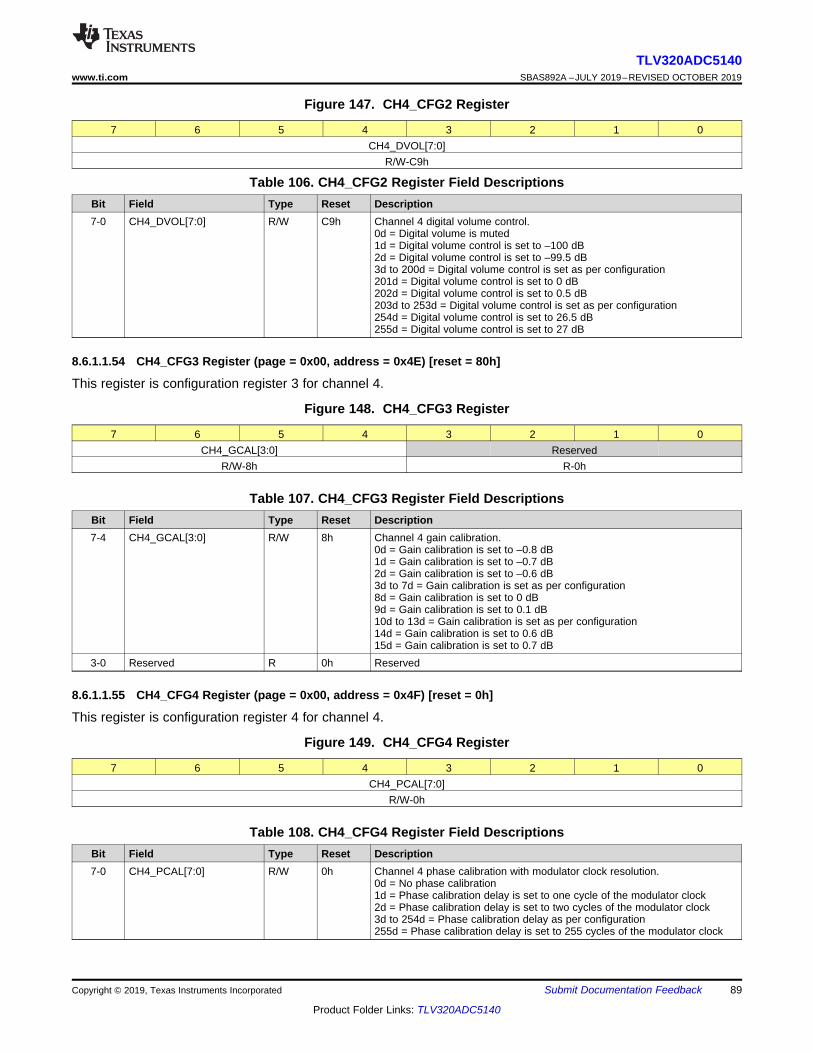
89
TLV320ADC5140www.ti.com SBAS892A –JULY 2019–REVISED OCTOBER 2019
Product Folder Links: TLV320ADC5140
Submit Documentation FeedbackCopyright © 2019, Texas Instruments Incorporated
Figure 147. CH4_CFG2 Register
7 6 5 4 3 2 1 0CH4_DVOL[7:0]
R/W-C9h
Table 106. CH4_CFG2 Register Field DescriptionsBit Field Type Reset Description7-0 CH4_DVOL[7:0] R/W C9h Channel 4 digital volume control.
0d = Digital volume is muted1d = Digital volume control is set to –100 dB2d = Digital volume control is set to –99.5 dB3d to 200d = Digital volume control is set as per configuration201d = Digital volume control is set to 0 dB202d = Digital volume control is set to 0.5 dB203d to 253d = Digital volume control is set as per configuration254d = Digital volume control is set to 26.5 dB255d = Digital volume control is set to 27 dB
8.6.1.1.54 CH4_CFG3 Register (page = 0x00, address = 0x4E) [reset = 80h]
This register is configuration register 3 for channel 4.
Figure 148. CH4_CFG3 Register
7 6 5 4 3 2 1 0CH4_GCAL[3:0] Reserved
R/W-8h R-0h
Table 107. CH4_CFG3 Register Field DescriptionsBit Field Type Reset Description7-4 CH4_GCAL[3:0] R/W 8h Channel 4 gain calibration.
0d = Gain calibration is set to –0.8 dB1d = Gain calibration is set to –0.7 dB2d = Gain calibration is set to –0.6 dB3d to 7d = Gain calibration is set as per configuration8d = Gain calibration is set to 0 dB9d = Gain calibration is set to 0.1 dB10d to 13d = Gain calibration is set as per configuration14d = Gain calibration is set to 0.6 dB15d = Gain calibration is set to 0.7 dB
3-0 Reserved R 0h Reserved
8.6.1.1.55 CH4_CFG4 Register (page = 0x00, address = 0x4F) [reset = 0h]
This register is configuration register 4 for channel 4.
Figure 149. CH4_CFG4 Register
7 6 5 4 3 2 1 0CH4_PCAL[7:0]
R/W-0h
Table 108. CH4_CFG4 Register Field DescriptionsBit Field Type Reset Description7-0 CH4_PCAL[7:0] R/W 0h Channel 4 phase calibration with modulator clock resolution.
0d = No phase calibration1d = Phase calibration delay is set to one cycle of the modulator clock2d = Phase calibration delay is set to two cycles of the modulator clock3d to 254d = Phase calibration delay as per configuration255d = Phase calibration delay is set to 255 cycles of the modulator clock
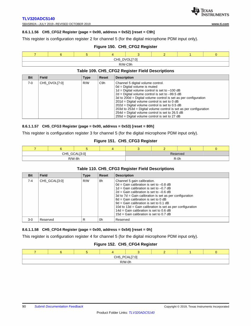
90
TLV320ADC5140SBAS892A –JULY 2019–REVISED OCTOBER 2019 www.ti.com
Product Folder Links: TLV320ADC5140
Submit Documentation Feedback Copyright © 2019, Texas Instruments Incorporated
8.6.1.1.56 CH5_CFG2 Register (page = 0x00, address = 0x52) [reset = C9h]
This register is configuration register 2 for channel 5 (for the digital microphone PDM input only).
Figure 150. CH5_CFG2 Register
7 6 5 4 3 2 1 0CH5_DVOL[7:0]
R/W-C9h
Table 109. CH5_CFG2 Register Field DescriptionsBit Field Type Reset Description7-0 CH5_DVOL[7:0] R/W C9h Channel 5 digital volume control.
0d = Digital volume is muted1d = Digital volume control is set to –100 dB2d = Digital volume control is set to –99.5 dB3d to 200d = Digital volume control is set as per configuration201d = Digital volume control is set to 0 dB202d = Digital volume control is set to 0.5 dB203d to 253d = Digital volume control is set as per configuration254d = Digital volume control is set to 26.5 dB255d = Digital volume control is set to 27 dB
8.6.1.1.57 CH5_CFG3 Register (page = 0x00, address = 0x53) [reset = 80h]
This register is configuration register 3 for channel 5 (for the digital microphone PDM input only).
Figure 151. CH5_CFG3 Register
7 6 5 4 3 2 1 0CH5_GCAL[3:0] Reserved
R/W-8h R-0h
Table 110. CH5_CFG3 Register Field DescriptionsBit Field Type Reset Description7-4 CH5_GCAL[3:0] R/W 8h Channel 5 gain calibration.
0d = Gain calibration is set to –0.8 dB1d = Gain calibration is set to –0.7 dB2d = Gain calibration is set to –0.6 dB3d to 7d = Gain calibration is set as per configuration8d = Gain calibration is set to 0 dB9d = Gain calibration is set to 0.1 dB10d to 13d = Gain calibration is set as per configuration14d = Gain calibration is set to 0.6 dB15d = Gain calibration is set to 0.7 dB
3-0 Reserved R 0h Reserved
8.6.1.1.58 CH5_CFG4 Register (page = 0x00, address = 0x54) [reset = 0h]
This register is configuration register 4 for channel 5 (for the digital microphone PDM input only).
Figure 152. CH5_CFG4 Register
7 6 5 4 3 2 1 0CH5_PCAL[7:0]
R/W-0h
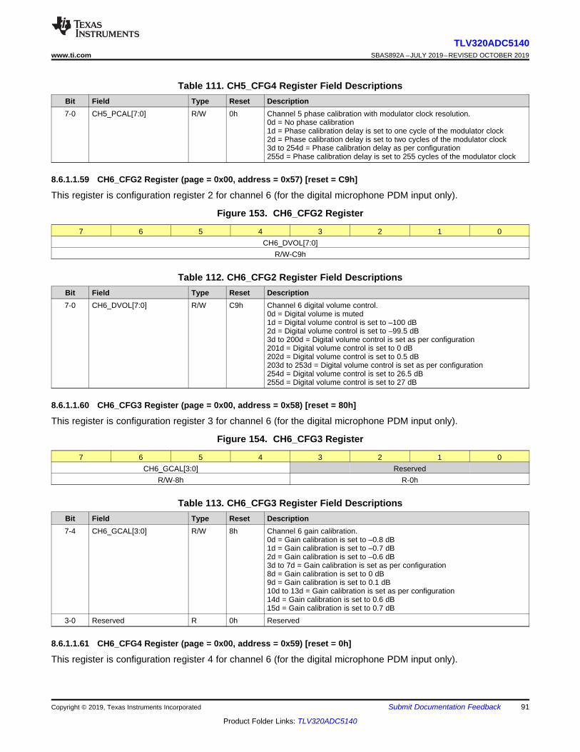
91
TLV320ADC5140www.ti.com SBAS892A –JULY 2019–REVISED OCTOBER 2019
Product Folder Links: TLV320ADC5140
Submit Documentation FeedbackCopyright © 2019, Texas Instruments Incorporated
Table 111. CH5_CFG4 Register Field DescriptionsBit Field Type Reset Description7-0 CH5_PCAL[7:0] R/W 0h Channel 5 phase calibration with modulator clock resolution.
0d = No phase calibration1d = Phase calibration delay is set to one cycle of the modulator clock2d = Phase calibration delay is set to two cycles of the modulator clock3d to 254d = Phase calibration delay as per configuration255d = Phase calibration delay is set to 255 cycles of the modulator clock
8.6.1.1.59 CH6_CFG2 Register (page = 0x00, address = 0x57) [reset = C9h]
This register is configuration register 2 for channel 6 (for the digital microphone PDM input only).
Figure 153. CH6_CFG2 Register
7 6 5 4 3 2 1 0CH6_DVOL[7:0]
R/W-C9h
Table 112. CH6_CFG2 Register Field DescriptionsBit Field Type Reset Description7-0 CH6_DVOL[7:0] R/W C9h Channel 6 digital volume control.
0d = Digital volume is muted1d = Digital volume control is set to –100 dB2d = Digital volume control is set to –99.5 dB3d to 200d = Digital volume control is set as per configuration201d = Digital volume control is set to 0 dB202d = Digital volume control is set to 0.5 dB203d to 253d = Digital volume control is set as per configuration254d = Digital volume control is set to 26.5 dB255d = Digital volume control is set to 27 dB
8.6.1.1.60 CH6_CFG3 Register (page = 0x00, address = 0x58) [reset = 80h]
This register is configuration register 3 for channel 6 (for the digital microphone PDM input only).
Figure 154. CH6_CFG3 Register
7 6 5 4 3 2 1 0CH6_GCAL[3:0] Reserved
R/W-8h R-0h
Table 113. CH6_CFG3 Register Field DescriptionsBit Field Type Reset Description7-4 CH6_GCAL[3:0] R/W 8h Channel 6 gain calibration.
0d = Gain calibration is set to –0.8 dB1d = Gain calibration is set to –0.7 dB2d = Gain calibration is set to –0.6 dB3d to 7d = Gain calibration is set as per configuration8d = Gain calibration is set to 0 dB9d = Gain calibration is set to 0.1 dB10d to 13d = Gain calibration is set as per configuration14d = Gain calibration is set to 0.6 dB15d = Gain calibration is set to 0.7 dB
3-0 Reserved R 0h Reserved
8.6.1.1.61 CH6_CFG4 Register (page = 0x00, address = 0x59) [reset = 0h]
This register is configuration register 4 for channel 6 (for the digital microphone PDM input only).
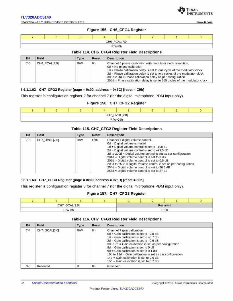
92
TLV320ADC5140SBAS892A –JULY 2019–REVISED OCTOBER 2019 www.ti.com
Product Folder Links: TLV320ADC5140
Submit Documentation Feedback Copyright © 2019, Texas Instruments Incorporated
Figure 155. CH6_CFG4 Register
7 6 5 4 3 2 1 0CH6_PCAL[7:0]
R/W-0h
Table 114. CH6_CFG4 Register Field DescriptionsBit Field Type Reset Description7-0 CH6_PCAL[7:0] R/W 0h Channel 6 phase calibration with modulator clock resolution.
0d = No phase calibration1d = Phase calibration delay is set to one cycle of the modulator clock2d = Phase calibration delay is set to two cycles of the modulator clock3d to 254d = Phase calibration delay as per configuration255d = Phase calibration delay is set to 255 cycles of the modulator clock
8.6.1.1.62 CH7_CFG2 Register (page = 0x00, address = 0x5C) [reset = C9h]
This register is configuration register 2 for channel 7 (for the digital microphone PDM input only).
Figure 156. CH7_CFG2 Register
7 6 5 4 3 2 1 0CH7_DVOL[7:0]
R/W-C9h
Table 115. CH7_CFG2 Register Field DescriptionsBit Field Type Reset Description7-0 CH7_DVOL[7:0] R/W C9h Channel 7 digital volume control.
0d = Digital volume is muted1d = Digital volume control is set to –100 dB2d = Digital volume control is set to –99.5 dB3d to 200d = Digital volume control is set as per configuration201d = Digital volume control is set to 0 dB202d = Digital volume control is set to 0.5 dB203d to 253d = Digital volume control is set as per configuration254d = Digital volume control is set to 26.5 dB255d = Digital volume control is set to 27 dB
8.6.1.1.63 CH7_CFG3 Register (page = 0x00, address = 0x5D) [reset = 80h]
This register is configuration register 3 for channel 7 (for the digital microphone PDM input only).
Figure 157. CH7_CFG3 Register
7 6 5 4 3 2 1 0CH7_GCAL[3:0] Reserved
R/W-8h R-0h
Table 116. CH7_CFG3 Register Field DescriptionsBit Field Type Reset Description7-4 CH7_GCAL[3:0] R/W 8h Channel 7 gain calibration.
0d = Gain calibration is set to –0.8 dB1d = Gain calibration is set to –0.7 dB2d = Gain calibration is set to –0.6 dB3d to 7d = Gain calibration is set as per configuration8d = Gain calibration is set to 0 dB9d = Gain calibration is set to 0.1 dB10d to 13d = Gain calibration is set as per configuration14d = Gain calibration is set to 0.6 dB15d = Gain calibration is set to 0.7 dB
3-0 Reserved R 0h Reserved
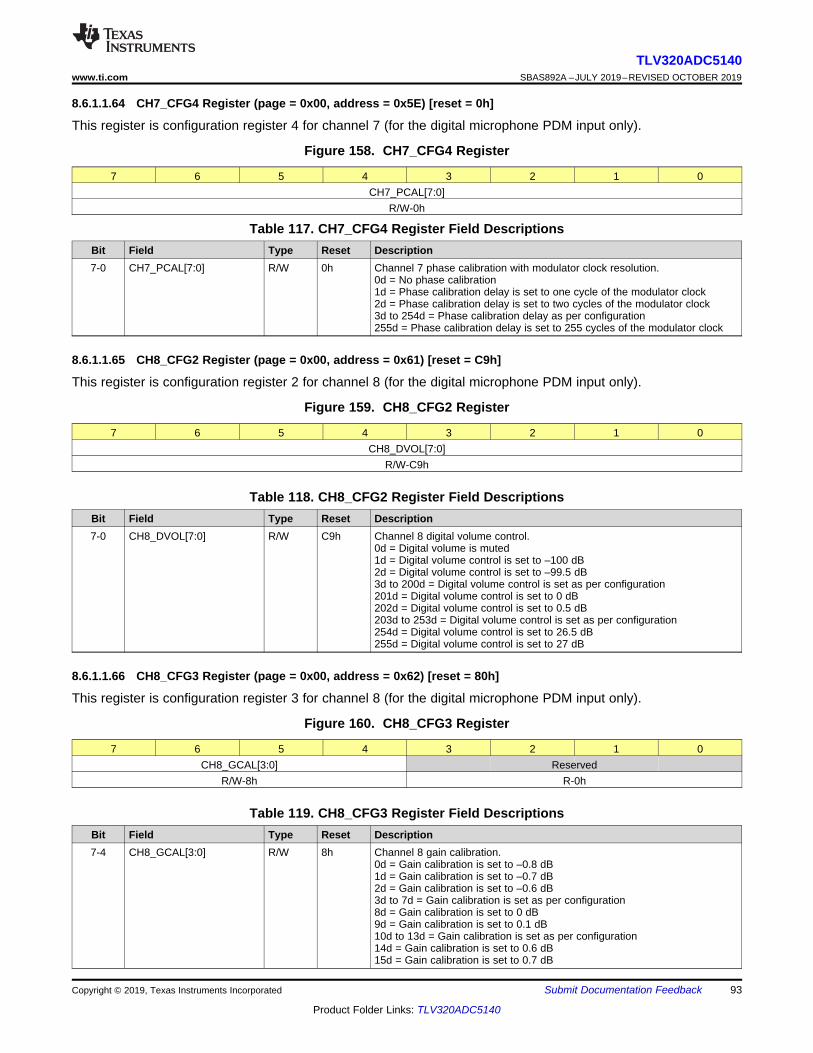
93
TLV320ADC5140www.ti.com SBAS892A –JULY 2019–REVISED OCTOBER 2019
Product Folder Links: TLV320ADC5140
Submit Documentation FeedbackCopyright © 2019, Texas Instruments Incorporated
8.6.1.1.64 CH7_CFG4 Register (page = 0x00, address = 0x5E) [reset = 0h]
This register is configuration register 4 for channel 7 (for the digital microphone PDM input only).
Figure 158. CH7_CFG4 Register
7 6 5 4 3 2 1 0CH7_PCAL[7:0]
R/W-0h
Table 117. CH7_CFG4 Register Field DescriptionsBit Field Type Reset Description7-0 CH7_PCAL[7:0] R/W 0h Channel 7 phase calibration with modulator clock resolution.
0d = No phase calibration1d = Phase calibration delay is set to one cycle of the modulator clock2d = Phase calibration delay is set to two cycles of the modulator clock3d to 254d = Phase calibration delay as per configuration255d = Phase calibration delay is set to 255 cycles of the modulator clock
8.6.1.1.65 CH8_CFG2 Register (page = 0x00, address = 0x61) [reset = C9h]
This register is configuration register 2 for channel 8 (for the digital microphone PDM input only).
Figure 159. CH8_CFG2 Register
7 6 5 4 3 2 1 0CH8_DVOL[7:0]
R/W-C9h
Table 118. CH8_CFG2 Register Field DescriptionsBit Field Type Reset Description7-0 CH8_DVOL[7:0] R/W C9h Channel 8 digital volume control.
0d = Digital volume is muted1d = Digital volume control is set to –100 dB2d = Digital volume control is set to –99.5 dB3d to 200d = Digital volume control is set as per configuration201d = Digital volume control is set to 0 dB202d = Digital volume control is set to 0.5 dB203d to 253d = Digital volume control is set as per configuration254d = Digital volume control is set to 26.5 dB255d = Digital volume control is set to 27 dB
8.6.1.1.66 CH8_CFG3 Register (page = 0x00, address = 0x62) [reset = 80h]
This register is configuration register 3 for channel 8 (for the digital microphone PDM input only).
Figure 160. CH8_CFG3 Register
7 6 5 4 3 2 1 0CH8_GCAL[3:0] Reserved
R/W-8h R-0h
Table 119. CH8_CFG3 Register Field DescriptionsBit Field Type Reset Description7-4 CH8_GCAL[3:0] R/W 8h Channel 8 gain calibration.
0d = Gain calibration is set to –0.8 dB1d = Gain calibration is set to –0.7 dB2d = Gain calibration is set to –0.6 dB3d to 7d = Gain calibration is set as per configuration8d = Gain calibration is set to 0 dB9d = Gain calibration is set to 0.1 dB10d to 13d = Gain calibration is set as per configuration14d = Gain calibration is set to 0.6 dB15d = Gain calibration is set to 0.7 dB
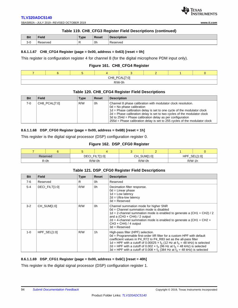
94
TLV320ADC5140SBAS892A –JULY 2019–REVISED OCTOBER 2019 www.ti.com
Product Folder Links: TLV320ADC5140
Submit Documentation Feedback Copyright © 2019, Texas Instruments Incorporated
Table 119. CH8_CFG3 Register Field Descriptions (continued)Bit Field Type Reset Description3-0 Reserved R 0h Reserved
8.6.1.1.67 CH8_CFG4 Register (page = 0x00, address = 0x63) [reset = 0h]
This register is configuration register 4 for channel 8 (for the digital microphone PDM input only).
Figure 161. CH8_CFG4 Register
7 6 5 4 3 2 1 0CH8_PCAL[7:0]
R/W-0h
Table 120. CH8_CFG4 Register Field DescriptionsBit Field Type Reset Description7-0 CH8_PCAL[7:0] R/W 0h Channel 8 phase calibration with modulator clock resolution.
0d = No phase calibration1d = Phase calibration delay is set to one cycle of the modulator clock2d = Phase calibration delay is set to two cycles of the modulator clock3d to 254d = Phase calibration delay as per configuration255d = Phase calibration delay is set to 255 cycles of the modulator clock
8.6.1.1.68 DSP_CFG0 Register (page = 0x00, address = 0x6B) [reset = 1h]
This register is the digital signal processor (DSP) configuration register 0.
Figure 162. DSP_CFG0 Register
7 6 5 4 3 2 1 0Reserved DECI_FILT[1:0] CH_SUM[1:0] HPF_SEL[1:0]
R-0h R/W-0h R/W-0h R/W-1h
Table 121. DSP_CFG0 Register Field DescriptionsBit Field Type Reset Description7-6 Reserved R 0h Reserved5-4 DECI_FILT[1:0] R/W 0h Decimation filter response.
0d = Linear phase1d = Low latency2d = Ultra-low latency3d = Reserved
3-2 CH_SUM[1:0] R/W 0h Channel summation mode for higher SNR0d = Channel summation mode is disabled1d = 2-channel summation mode is enabled to generate a (CH1 + CH2) / 2and a (CH3 + CH4) / 2 output2d = 4-channel summation mode is enabled to generate a (CH1 + CH2 +CH3 + CH4) / 4 output3d = Reserved
1-0 HPF_SEL[1:0] R/W 1h High-pass filter (HPF) selection.0d = Programmable first-order IIR filter for a custom HPF with defaultcoefficient values in P4_R72 to P4_R83 set as the all-pass filter1d = HPF with a cutoff of 0.00025 × fS (12 Hz at fS = 48 kHz) is selected2d = HPF with a cutoff of 0.002 × fS (96 Hz at fS = 48 kHz) is selected3d = HPF with a cutoff of 0.008 × fS (384 Hz at fS = 48 kHz) is selected
8.6.1.1.69 DSP_CFG1 Register (page = 0x00, address = 0x6C) [reset = 40h]
This register is the digital signal processor (DSP) configuration register 1.
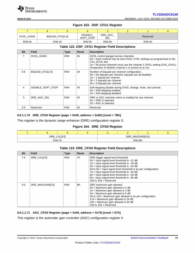
95
TLV320ADC5140www.ti.com SBAS892A –JULY 2019–REVISED OCTOBER 2019
Product Folder Links: TLV320ADC5140
Submit Documentation FeedbackCopyright © 2019, Texas Instruments Incorporated
Figure 163. DSP_CFG1 Register
7 6 5 4 3 2 1 0
DVOL_GANG BIQUAD_CFG[1:0] DISABLE_SOFT_STEP
DRE_AGC_SEL Reserved
R/W-0h R/W-2h R/W-0h R/W-0h R/W-0h
Table 122. DSP_CFG1 Register Field DescriptionsBit Field Type Reset Description7 DVOL_GANG R/W 0h DVOL control ganged across channels.
0d = Each channel has its own DVOL CTRL settings as programmed in theCHx_DVOL bits1d = All active channels must use the channel 1 DVOL setting (CH1_DVOL)irrespective of whether channel 1 is turned on or not
6-5 BIQUAD_CFG[1:0] R/W 2h Number of biquads per channel configuration.0d = No biquads per channel; biquads are all disabled1d = 1 biquad per channel2d = 2 biquads per channel3d = 3 biquads per channel
4 DISABLE_SOFT_STEP R/W 0h Soft-stepping disable during DVOL change, mute, and unmute.0d = Soft-stepping enabled1d = Soft-stepping disabled
3 DRE_AGC_SEL R/W 0h DRE or AGC selection when is enabled for any channel.0d = DRE is selected1d = AGC is selected
2-0 Reserved R/W 0h Reserved
8.6.1.1.70 DRE_CFG0 Register (page = 0x00, address = 0x6D) [reset = 7Bh]
This register is the dynamic range enhancer (DRE) configuration register 0.
Figure 164. DRE_CFG0 Register
7 6 5 4 3 2 1 0DRE_LVL[3:0] DRE_MAXGAIN[3:0]
R/W-7h R/W-Bh
Table 123. DRE_CFG0 Register Field DescriptionsBit Field Type Reset Description7-4 DRE_LVL[3:0] R/W 7h DRE trigger signal level threshold.
0d = Input signal level threshold is –12 dB1d = Input signal level threshold is –18 dB2d = Input signal level threshold is –24 dB3d to 6d = Input signal level threshold is as per configuration7d = Input signal level threshold is –54 dB8d = Input signal level threshold is –60 dB9d = Input signal level threshold is –66 dB10d to 15d = Reserved
3-0 DRE_MAXGAIN[3:0] R/W Bh DRE maximum gain allowed.0d = Maximum gain allowed is 2 dB1d = Maximum gain allowed is 4 dB2d = Maximum gain allowed is 6 dB3d to 10d = Maximum gain allowed is as per configuration11d = Maximum gain allowed is 24 dB12d = Maximum gain allowed is 26 dB13d to 15d = Reserved
8.6.1.1.71 AGC_CFG0 Register (page = 0x00, address = 0x70) [reset = E7h]
This register is the automatic gain controller (AGC) configuration register 0.
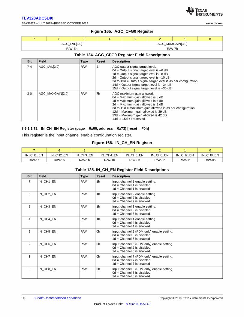
96
TLV320ADC5140SBAS892A –JULY 2019–REVISED OCTOBER 2019 www.ti.com
Product Folder Links: TLV320ADC5140
Submit Documentation Feedback Copyright © 2019, Texas Instruments Incorporated
Figure 165. AGC_CFG0 Register
7 6 5 4 3 2 1 0AGC_LVL[3:0] AGC_MAXGAIN[3:0]
R/W-Eh R/W-7h
Table 124. AGC_CFG0 Register Field DescriptionsBit Field Type Reset Description7-4 AGC_LVL[3:0] R/W Eh AGC output signal target level.
0d = Output signal target level is –6 dB1d = Output signal target level is –8 dB2d = Output signal target level is –10 dB3d to 13d = Output signal target level is as per configuration14d = Output signal target level is –34 dB15d = Output signal target level is –36 dB
3-0 AGC_MAXGAIN[3:0] R/W 7h AGC maximum gain allowed.0d = Maximum gain allowed is 3 dB1d = Maximum gain allowed is 6 dB2d = Maximum gain allowed is 9 dB3d to 11d = Maximum gain allowed is as per configuration12d = Maximum gain allowed is 39 dB13d = Maximum gain allowed is 42 dB14d to 15d = Reserved
8.6.1.1.72 IN_CH_EN Register (page = 0x00, address = 0x73) [reset = F0h]
This register is the input channel enable configuration register.
Figure 166. IN_CH_EN Register
7 6 5 4 3 2 1 0IN_CH1_EN IN_CH2_EN IN_CH3_EN IN_CH4_EN IN_CH5_EN IN_CH6_EN IN_CH7_EN IN_CH8_EN
R/W-1h R/W-1h R/W-1h R/W-1h R/W-0h R/W-0h R/W-0h R/W-0h
Table 125. IN_CH_EN Register Field DescriptionsBit Field Type Reset Description7 IN_CH1_EN R/W 1h Input channel 1 enable setting.
0d = Channel 1 is disabled1d = Channel 1 is enabled
6 IN_CH2_EN R/W 1h Input channel 2 enable setting.0d = Channel 2 is disabled1d = Channel 2 is enabled
5 IN_CH3_EN R/W 1h Input channel 3 enable setting.0d = Channel 3 is disabled1d = Channel 3 is enabled
4 IN_CH4_EN R/W 1h Input channel 4 enable setting.0d = Channel 4 is disabled1d = Channel 4 is enabled
3 IN_CH5_EN R/W 0h Input channel 5 (PDM only) enable setting.0d = Channel 5 is disabled1d = Channel 5 is enabled
2 IN_CH6_EN R/W 0h Input channel 6 (PDM only) enable setting.0d = Channel 6 is disabled1d = Channel 6 is enabled
1 IN_CH7_EN R/W 0h Input channel 7 (PDM only) enable setting.0d = Channel 7 is disabled1d = Channel 7 is enabled
0 IN_CH8_EN R/W 0h Input channel 8 (PDM only) enable setting.0d = Channel 8 is disabled1d = Channel 8 is enabled
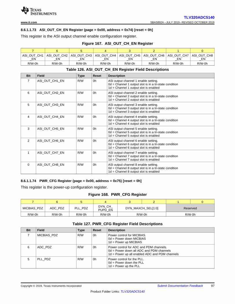
97
TLV320ADC5140www.ti.com SBAS892A –JULY 2019–REVISED OCTOBER 2019
Product Folder Links: TLV320ADC5140
Submit Documentation FeedbackCopyright © 2019, Texas Instruments Incorporated
8.6.1.1.73 ASI_OUT_CH_EN Register (page = 0x00, address = 0x74) [reset = 0h]
This register is the ASI output channel enable configuration register.
Figure 167. ASI_OUT_CH_EN Register
7 6 5 4 3 2 1 0ASI_OUT_CH1
_ENASI_OUT_CH2
_ENASI_OUT_CH3
_ENASI_OUT_CH4
_ENASI_OUT_CH5
_ENASI_OUT_CH6
_ENASI_OUT_CH7
_ENASI_OUT_CH8
_ENR/W-0h R/W-0h R/W-0h R/W-0h R/W-0h R/W-0h R/W-0h R/W-0h
Table 126. ASI_OUT_CH_EN Register Field DescriptionsBit Field Type Reset Description7 ASI_OUT_CH1_EN R/W 0h ASI output channel 1 enable setting.
0d = Channel 1 output slot is in a tri-state condition1d = Channel 1 output slot is enabled
6 ASI_OUT_CH2_EN R/W 0h ASI output channel 2 enable setting.0d = Channel 2 output slot is in a tri-state condition1d = Channel 2 output slot is enabled
5 ASI_OUT_CH3_EN R/W 0h ASI output channel 3 enable setting.0d = Channel 3 output slot is in a tri-state condition1d = Channel 3 output slot is enabled
4 ASI_OUT_CH4_EN R/W 0h ASI output channel 4 enable setting.0d = Channel 4 output slot is in a tri-state condition1d = Channel 4 output slot is enabled
3 ASI_OUT_CH5_EN R/W 0h ASI output channel 5 enable setting.0d = Channel 5 output slot is in a tri-state condition1d = Channel 5 output slot is enabled
2 ASI_OUT_CH6_EN R/W 0h ASI output channel 6 enable setting.0d = Channel 6 output slot is in a tri-state condition1d = Channel 6 output slot is enabled
1 ASI_OUT_CH7_EN R/W 0h ASI output channel 7 enable setting.0d = Channel 7 output slot is in a tri-state condition1d = Channel 7 output slot is enabled
0 ASI_OUT_CH8_EN R/W 0h ASI output channel 8 enable setting.0d = Channel 8 output slot is in a tri-state condition1d = Channel 8 output slot is enabled
8.6.1.1.74 PWR_CFG Register (page = 0x00, address = 0x75) [reset = 0h]
This register is the power-up configuration register.
Figure 168. PWR_CFG Register
7 6 5 4 3 2 1 0
MICBIAS_PDZ ADC_PDZ PLL_PDZ DYN_CH_PUPD_EN DYN_MAXCH_SEL[1:0] Reserved
R/W-0h R/W-0h R/W-0h R/W-0h R/W-0h R/W-0h
Table 127. PWR_CFG Register Field DescriptionsBit Field Type Reset Description7 MICBIAS_PDZ R/W 0h Power control for MICBIAS.
0d = Power down MICBIAS1d = Power up MICBIAS
6 ADC_PDZ R/W 0h Power control for ADC and PDM channels.0d = Power down all ADC and PDM channels1d = Power up all enabled ADC and PDM channels
5 PLL_PDZ R/W 0h Power control for the PLL.0d = Power down the PLL1d = Power up the PLL
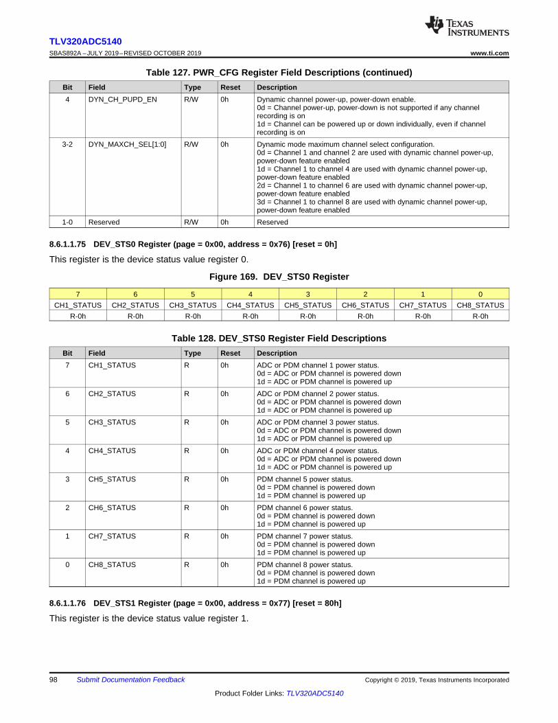
98
TLV320ADC5140SBAS892A –JULY 2019–REVISED OCTOBER 2019 www.ti.com
Product Folder Links: TLV320ADC5140
Submit Documentation Feedback Copyright © 2019, Texas Instruments Incorporated
Table 127. PWR_CFG Register Field Descriptions (continued)Bit Field Type Reset Description4 DYN_CH_PUPD_EN R/W 0h Dynamic channel power-up, power-down enable.
0d = Channel power-up, power-down is not supported if any channelrecording is on1d = Channel can be powered up or down individually, even if channelrecording is on
3-2 DYN_MAXCH_SEL[1:0] R/W 0h Dynamic mode maximum channel select configuration.0d = Channel 1 and channel 2 are used with dynamic channel power-up,power-down feature enabled1d = Channel 1 to channel 4 are used with dynamic channel power-up,power-down feature enabled2d = Channel 1 to channel 6 are used with dynamic channel power-up,power-down feature enabled3d = Channel 1 to channel 8 are used with dynamic channel power-up,power-down feature enabled
1-0 Reserved R/W 0h Reserved
8.6.1.1.75 DEV_STS0 Register (page = 0x00, address = 0x76) [reset = 0h]
This register is the device status value register 0.
Figure 169. DEV_STS0 Register
7 6 5 4 3 2 1 0CH1_STATUS CH2_STATUS CH3_STATUS CH4_STATUS CH5_STATUS CH6_STATUS CH7_STATUS CH8_STATUS
R-0h R-0h R-0h R-0h R-0h R-0h R-0h R-0h
Table 128. DEV_STS0 Register Field DescriptionsBit Field Type Reset Description7 CH1_STATUS R 0h ADC or PDM channel 1 power status.
0d = ADC or PDM channel is powered down1d = ADC or PDM channel is powered up
6 CH2_STATUS R 0h ADC or PDM channel 2 power status.0d = ADC or PDM channel is powered down1d = ADC or PDM channel is powered up
5 CH3_STATUS R 0h ADC or PDM channel 3 power status.0d = ADC or PDM channel is powered down1d = ADC or PDM channel is powered up
4 CH4_STATUS R 0h ADC or PDM channel 4 power status.0d = ADC or PDM channel is powered down1d = ADC or PDM channel is powered up
3 CH5_STATUS R 0h PDM channel 5 power status.0d = PDM channel is powered down1d = PDM channel is powered up
2 CH6_STATUS R 0h PDM channel 6 power status.0d = PDM channel is powered down1d = PDM channel is powered up
1 CH7_STATUS R 0h PDM channel 7 power status.0d = PDM channel is powered down1d = PDM channel is powered up
0 CH8_STATUS R 0h PDM channel 8 power status.0d = PDM channel is powered down1d = PDM channel is powered up
8.6.1.1.76 DEV_STS1 Register (page = 0x00, address = 0x77) [reset = 80h]
This register is the device status value register 1.
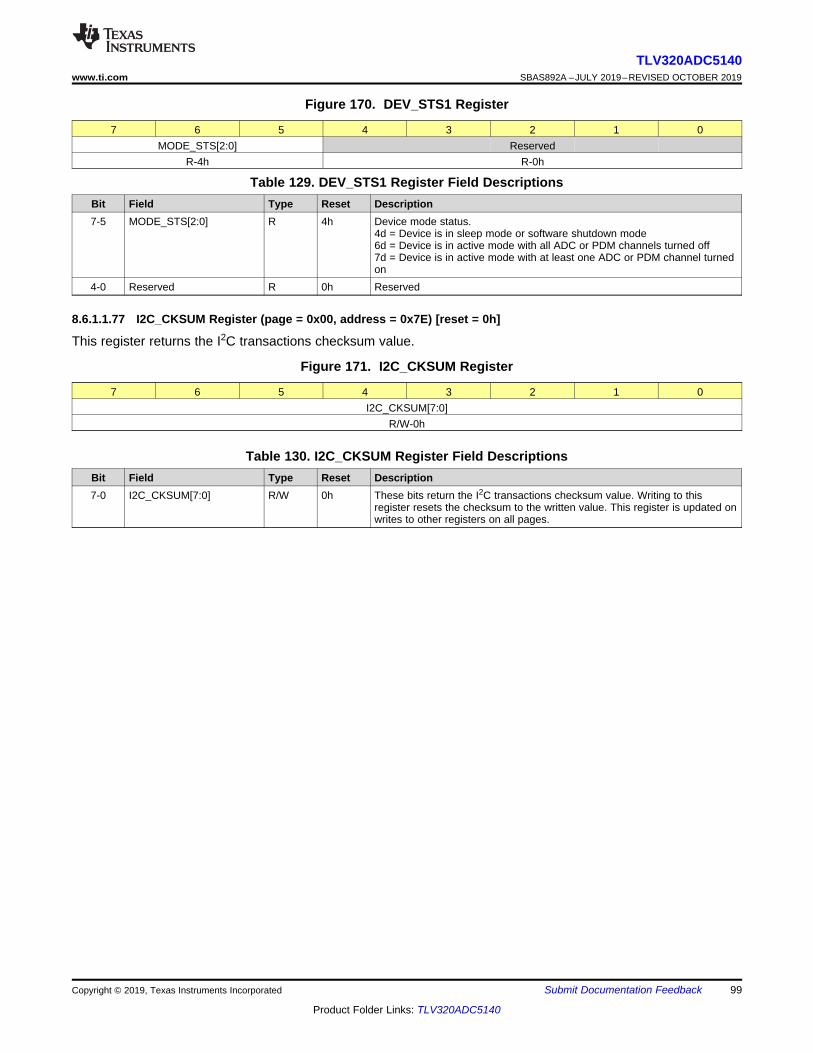
99
TLV320ADC5140www.ti.com SBAS892A –JULY 2019–REVISED OCTOBER 2019
Product Folder Links: TLV320ADC5140
Submit Documentation FeedbackCopyright © 2019, Texas Instruments Incorporated
Figure 170. DEV_STS1 Register
7 6 5 4 3 2 1 0MODE_STS[2:0] Reserved
R-4h R-0h
Table 129. DEV_STS1 Register Field DescriptionsBit Field Type Reset Description7-5 MODE_STS[2:0] R 4h Device mode status.
4d = Device is in sleep mode or software shutdown mode6d = Device is in active mode with all ADC or PDM channels turned off7d = Device is in active mode with at least one ADC or PDM channel turnedon
4-0 Reserved R 0h Reserved
8.6.1.1.77 I2C_CKSUM Register (page = 0x00, address = 0x7E) [reset = 0h]
This register returns the I2C transactions checksum value.
Figure 171. I2C_CKSUM Register
7 6 5 4 3 2 1 0I2C_CKSUM[7:0]
R/W-0h
Table 130. I2C_CKSUM Register Field DescriptionsBit Field Type Reset Description7-0 I2C_CKSUM[7:0] R/W 0h These bits return the I2C transactions checksum value. Writing to this
register resets the checksum to the written value. This register is updated onwrites to other registers on all pages.
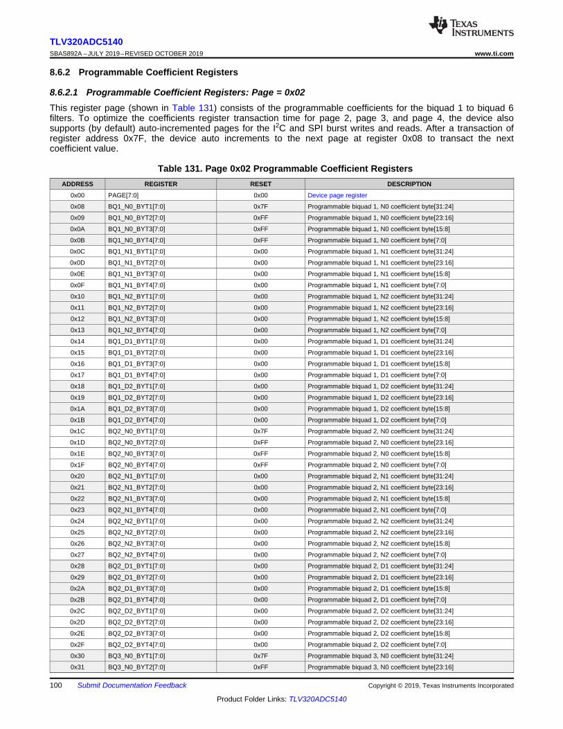
100
TLV320ADC5140SBAS892A –JULY 2019–REVISED OCTOBER 2019 www.ti.com
Product Folder Links: TLV320ADC5140
Submit Documentation Feedback Copyright © 2019, Texas Instruments Incorporated
8.6.2 Programmable Coefficient Registers
8.6.2.1 Programmable Coefficient Registers: Page = 0x02This register page (shown in Table 131) consists of the programmable coefficients for the biquad 1 to biquad 6filters. To optimize the coefficients register transaction time for page 2, page 3, and page 4, the device alsosupports (by default) auto-incremented pages for the I2C and SPI burst writes and reads. After a transaction ofregister address 0x7F, the device auto increments to the next page at register 0x08 to transact the nextcoefficient value.
Table 131. Page 0x02 Programmable Coefficient RegistersADDRESS REGISTER RESET DESCRIPTION
0x00 PAGE[7:0] 0x00 Device page register
0x08 BQ1_N0_BYT1[7:0] 0x7F Programmable biquad 1, N0 coefficient byte[31:24]
0x09 BQ1_N0_BYT2[7:0] 0xFF Programmable biquad 1, N0 coefficient byte[23:16]
0x0A BQ1_N0_BYT3[7:0] 0xFF Programmable biquad 1, N0 coefficient byte[15:8]
0x0B BQ1_N0_BYT4[7:0] 0xFF Programmable biquad 1, N0 coefficient byte[7:0]
0x0C BQ1_N1_BYT1[7:0] 0x00 Programmable biquad 1, N1 coefficient byte[31:24]
0x0D BQ1_N1_BYT2[7:0] 0x00 Programmable biquad 1, N1 coefficient byte[23:16]
0x0E BQ1_N1_BYT3[7:0] 0x00 Programmable biquad 1, N1 coefficient byte[15:8]
0x0F BQ1_N1_BYT4[7:0] 0x00 Programmable biquad 1, N1 coefficient byte[7:0]
0x10 BQ1_N2_BYT1[7:0] 0x00 Programmable biquad 1, N2 coefficient byte[31:24]
0x11 BQ1_N2_BYT2[7:0] 0x00 Programmable biquad 1, N2 coefficient byte[23:16]
0x12 BQ1_N2_BYT3[7:0] 0x00 Programmable biquad 1, N2 coefficient byte[15:8]
0x13 BQ1_N2_BYT4[7:0] 0x00 Programmable biquad 1, N2 coefficient byte[7:0]
0x14 BQ1_D1_BYT1[7:0] 0x00 Programmable biquad 1, D1 coefficient byte[31:24]
0x15 BQ1_D1_BYT2[7:0] 0x00 Programmable biquad 1, D1 coefficient byte[23:16]
0x16 BQ1_D1_BYT3[7:0] 0x00 Programmable biquad 1, D1 coefficient byte[15:8]
0x17 BQ1_D1_BYT4[7:0] 0x00 Programmable biquad 1, D1 coefficient byte[7:0]
0x18 BQ1_D2_BYT1[7:0] 0x00 Programmable biquad 1, D2 coefficient byte[31:24]
0x19 BQ1_D2_BYT2[7:0] 0x00 Programmable biquad 1, D2 coefficient byte[23:16]
0x1A BQ1_D2_BYT3[7:0] 0x00 Programmable biquad 1, D2 coefficient byte[15:8]
0x1B BQ1_D2_BYT4[7:0] 0x00 Programmable biquad 1, D2 coefficient byte[7:0]
0x1C BQ2_N0_BYT1[7:0] 0x7F Programmable biquad 2, N0 coefficient byte[31:24]
0x1D BQ2_N0_BYT2[7:0] 0xFF Programmable biquad 2, N0 coefficient byte[23:16]
0x1E BQ2_N0_BYT3[7:0] 0xFF Programmable biquad 2, N0 coefficient byte[15:8]
0x1F BQ2_N0_BYT4[7:0] 0xFF Programmable biquad 2, N0 coefficient byte[7:0]
0x20 BQ2_N1_BYT1[7:0] 0x00 Programmable biquad 2, N1 coefficient byte[31:24]
0x21 BQ2_N1_BYT2[7:0] 0x00 Programmable biquad 2, N1 coefficient byte[23:16]
0x22 BQ2_N1_BYT3[7:0] 0x00 Programmable biquad 2, N1 coefficient byte[15:8]
0x23 BQ2_N1_BYT4[7:0] 0x00 Programmable biquad 2, N1 coefficient byte[7:0]
0x24 BQ2_N2_BYT1[7:0] 0x00 Programmable biquad 2, N2 coefficient byte[31:24]
0x25 BQ2_N2_BYT2[7:0] 0x00 Programmable biquad 2, N2 coefficient byte[23:16]
0x26 BQ2_N2_BYT3[7:0] 0x00 Programmable biquad 2, N2 coefficient byte[15:8]
0x27 BQ2_N2_BYT4[7:0] 0x00 Programmable biquad 2, N2 coefficient byte[7:0]
0x28 BQ2_D1_BYT1[7:0] 0x00 Programmable biquad 2, D1 coefficient byte[31:24]
0x29 BQ2_D1_BYT2[7:0] 0x00 Programmable biquad 2, D1 coefficient byte[23:16]
0x2A BQ2_D1_BYT3[7:0] 0x00 Programmable biquad 2, D1 coefficient byte[15:8]
0x2B BQ2_D1_BYT4[7:0] 0x00 Programmable biquad 2, D1 coefficient byte[7:0]
0x2C BQ2_D2_BYT1[7:0] 0x00 Programmable biquad 2, D2 coefficient byte[31:24]
0x2D BQ2_D2_BYT2[7:0] 0x00 Programmable biquad 2, D2 coefficient byte[23:16]
0x2E BQ2_D2_BYT3[7:0] 0x00 Programmable biquad 2, D2 coefficient byte[15:8]
0x2F BQ2_D2_BYT4[7:0] 0x00 Programmable biquad 2, D2 coefficient byte[7:0]
0x30 BQ3_N0_BYT1[7:0] 0x7F Programmable biquad 3, N0 coefficient byte[31:24]
0x31 BQ3_N0_BYT2[7:0] 0xFF Programmable biquad 3, N0 coefficient byte[23:16]
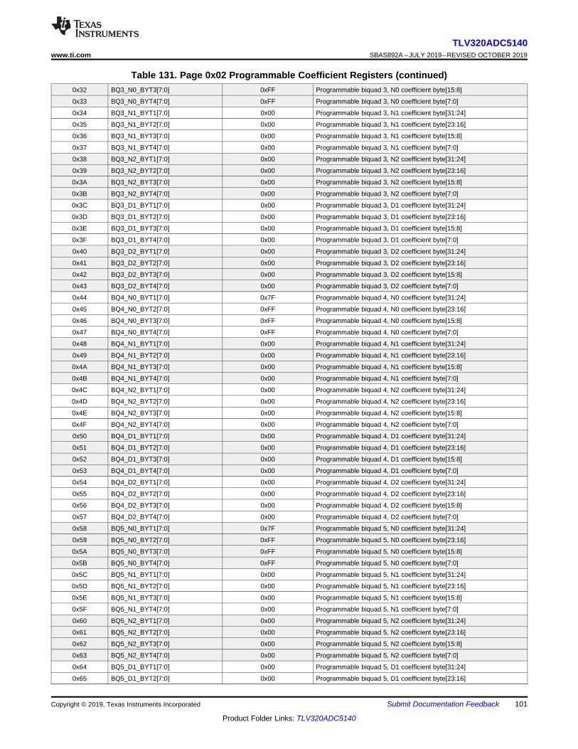
101
TLV320ADC5140www.ti.com SBAS892A –JULY 2019–REVISED OCTOBER 2019
Product Folder Links: TLV320ADC5140
Submit Documentation FeedbackCopyright © 2019, Texas Instruments Incorporated
Table 131. Page 0x02 Programmable Coefficient Registers (continued)0x32 BQ3_N0_BYT3[7:0] 0xFF Programmable biquad 3, N0 coefficient byte[15:8]
0x33 BQ3_N0_BYT4[7:0] 0xFF Programmable biquad 3, N0 coefficient byte[7:0]
0x34 BQ3_N1_BYT1[7:0] 0x00 Programmable biquad 3, N1 coefficient byte[31:24]
0x35 BQ3_N1_BYT2[7:0] 0x00 Programmable biquad 3, N1 coefficient byte[23:16]
0x36 BQ3_N1_BYT3[7:0] 0x00 Programmable biquad 3, N1 coefficient byte[15:8]
0x37 BQ3_N1_BYT4[7:0] 0x00 Programmable biquad 3, N1 coefficient byte[7:0]
0x38 BQ3_N2_BYT1[7:0] 0x00 Programmable biquad 3, N2 coefficient byte[31:24]
0x39 BQ3_N2_BYT2[7:0] 0x00 Programmable biquad 3, N2 coefficient byte[23:16]
0x3A BQ3_N2_BYT3[7:0] 0x00 Programmable biquad 3, N2 coefficient byte[15:8]
0x3B BQ3_N2_BYT4[7:0] 0x00 Programmable biquad 3, N2 coefficient byte[7:0]
0x3C BQ3_D1_BYT1[7:0] 0x00 Programmable biquad 3, D1 coefficient byte[31:24]
0x3D BQ3_D1_BYT2[7:0] 0x00 Programmable biquad 3, D1 coefficient byte[23:16]
0x3E BQ3_D1_BYT3[7:0] 0x00 Programmable biquad 3, D1 coefficient byte[15:8]
0x3F BQ3_D1_BYT4[7:0] 0x00 Programmable biquad 3, D1 coefficient byte[7:0]
0x40 BQ3_D2_BYT1[7:0] 0x00 Programmable biquad 3, D2 coefficient byte[31:24]
0x41 BQ3_D2_BYT2[7:0] 0x00 Programmable biquad 3, D2 coefficient byte[23:16]
0x42 BQ3_D2_BYT3[7:0] 0x00 Programmable biquad 3, D2 coefficient byte[15:8]
0x43 BQ3_D2_BYT4[7:0] 0x00 Programmable biquad 3, D2 coefficient byte[7:0]
0x44 BQ4_N0_BYT1[7:0] 0x7F Programmable biquad 4, N0 coefficient byte[31:24]
0x45 BQ4_N0_BYT2[7:0] 0xFF Programmable biquad 4, N0 coefficient byte[23:16]
0x46 BQ4_N0_BYT3[7:0] 0xFF Programmable biquad 4, N0 coefficient byte[15:8]
0x47 BQ4_N0_BYT4[7:0] 0xFF Programmable biquad 4, N0 coefficient byte[7:0]
0x48 BQ4_N1_BYT1[7:0] 0x00 Programmable biquad 4, N1 coefficient byte[31:24]
0x49 BQ4_N1_BYT2[7:0] 0x00 Programmable biquad 4, N1 coefficient byte[23:16]
0x4A BQ4_N1_BYT3[7:0] 0x00 Programmable biquad 4, N1 coefficient byte[15:8]
0x4B BQ4_N1_BYT4[7:0] 0x00 Programmable biquad 4, N1 coefficient byte[7:0]
0x4C BQ4_N2_BYT1[7:0] 0x00 Programmable biquad 4, N2 coefficient byte[31:24]
0x4D BQ4_N2_BYT2[7:0] 0x00 Programmable biquad 4, N2 coefficient byte[23:16]
0x4E BQ4_N2_BYT3[7:0] 0x00 Programmable biquad 4, N2 coefficient byte[15:8]
0x4F BQ4_N2_BYT4[7:0] 0x00 Programmable biquad 4, N2 coefficient byte[7:0]
0x50 BQ4_D1_BYT1[7:0] 0x00 Programmable biquad 4, D1 coefficient byte[31:24]
0x51 BQ4_D1_BYT2[7:0] 0x00 Programmable biquad 4, D1 coefficient byte[23:16]
0x52 BQ4_D1_BYT3[7:0] 0x00 Programmable biquad 4, D1 coefficient byte[15:8]
0x53 BQ4_D1_BYT4[7:0] 0x00 Programmable biquad 4, D1 coefficient byte[7:0]
0x54 BQ4_D2_BYT1[7:0] 0x00 Programmable biquad 4, D2 coefficient byte[31:24]
0x55 BQ4_D2_BYT2[7:0] 0x00 Programmable biquad 4, D2 coefficient byte[23:16]
0x56 BQ4_D2_BYT3[7:0] 0x00 Programmable biquad 4, D2 coefficient byte[15:8]
0x57 BQ4_D2_BYT4[7:0] 0x00 Programmable biquad 4, D2 coefficient byte[7:0]
0x58 BQ5_N0_BYT1[7:0] 0x7F Programmable biquad 5, N0 coefficient byte[31:24]
0x59 BQ5_N0_BYT2[7:0] 0xFF Programmable biquad 5, N0 coefficient byte[23:16]
0x5A BQ5_N0_BYT3[7:0] 0xFF Programmable biquad 5, N0 coefficient byte[15:8]
0x5B BQ5_N0_BYT4[7:0] 0xFF Programmable biquad 5, N0 coefficient byte[7:0]
0x5C BQ5_N1_BYT1[7:0] 0x00 Programmable biquad 5, N1 coefficient byte[31:24]
0x5D BQ5_N1_BYT2[7:0] 0x00 Programmable biquad 5, N1 coefficient byte[23:16]
0x5E BQ5_N1_BYT3[7:0] 0x00 Programmable biquad 5, N1 coefficient byte[15:8]
0x5F BQ5_N1_BYT4[7:0] 0x00 Programmable biquad 5, N1 coefficient byte[7:0]
0x60 BQ5_N2_BYT1[7:0] 0x00 Programmable biquad 5, N2 coefficient byte[31:24]
0x61 BQ5_N2_BYT2[7:0] 0x00 Programmable biquad 5, N2 coefficient byte[23:16]
0x62 BQ5_N2_BYT3[7:0] 0x00 Programmable biquad 5, N2 coefficient byte[15:8]
0x63 BQ5_N2_BYT4[7:0] 0x00 Programmable biquad 5, N2 coefficient byte[7:0]
0x64 BQ5_D1_BYT1[7:0] 0x00 Programmable biquad 5, D1 coefficient byte[31:24]
0x65 BQ5_D1_BYT2[7:0] 0x00 Programmable biquad 5, D1 coefficient byte[23:16]
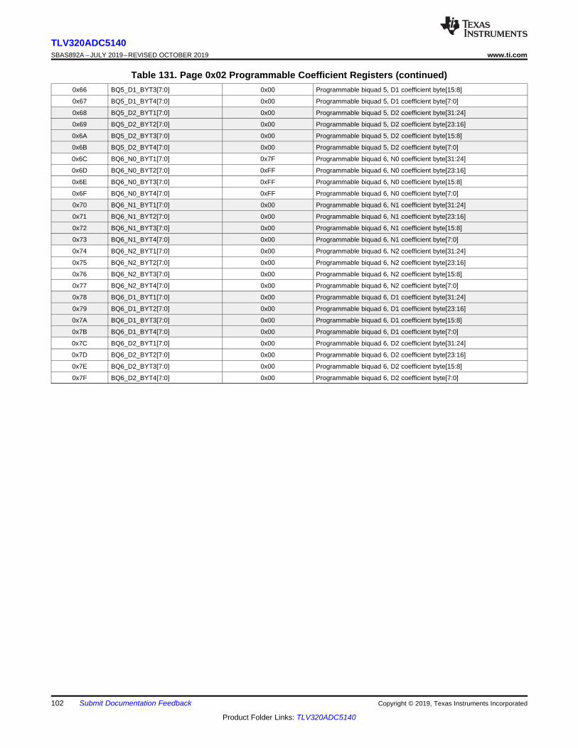
102
TLV320ADC5140SBAS892A –JULY 2019–REVISED OCTOBER 2019 www.ti.com
Product Folder Links: TLV320ADC5140
Submit Documentation Feedback Copyright © 2019, Texas Instruments Incorporated
Table 131. Page 0x02 Programmable Coefficient Registers (continued)0x66 BQ5_D1_BYT3[7:0] 0x00 Programmable biquad 5, D1 coefficient byte[15:8]
0x67 BQ5_D1_BYT4[7:0] 0x00 Programmable biquad 5, D1 coefficient byte[7:0]
0x68 BQ5_D2_BYT1[7:0] 0x00 Programmable biquad 5, D2 coefficient byte[31:24]
0x69 BQ5_D2_BYT2[7:0] 0x00 Programmable biquad 5, D2 coefficient byte[23:16]
0x6A BQ5_D2_BYT3[7:0] 0x00 Programmable biquad 5, D2 coefficient byte[15:8]
0x6B BQ5_D2_BYT4[7:0] 0x00 Programmable biquad 5, D2 coefficient byte[7:0]
0x6C BQ6_N0_BYT1[7:0] 0x7F Programmable biquad 6, N0 coefficient byte[31:24]
0x6D BQ6_N0_BYT2[7:0] 0xFF Programmable biquad 6, N0 coefficient byte[23:16]
0x6E BQ6_N0_BYT3[7:0] 0xFF Programmable biquad 6, N0 coefficient byte[15:8]
0x6F BQ6_N0_BYT4[7:0] 0xFF Programmable biquad 6, N0 coefficient byte[7:0]
0x70 BQ6_N1_BYT1[7:0] 0x00 Programmable biquad 6, N1 coefficient byte[31:24]
0x71 BQ6_N1_BYT2[7:0] 0x00 Programmable biquad 6, N1 coefficient byte[23:16]
0x72 BQ6_N1_BYT3[7:0] 0x00 Programmable biquad 6, N1 coefficient byte[15:8]
0x73 BQ6_N1_BYT4[7:0] 0x00 Programmable biquad 6, N1 coefficient byte[7:0]
0x74 BQ6_N2_BYT1[7:0] 0x00 Programmable biquad 6, N2 coefficient byte[31:24]
0x75 BQ6_N2_BYT2[7:0] 0x00 Programmable biquad 6, N2 coefficient byte[23:16]
0x76 BQ6_N2_BYT3[7:0] 0x00 Programmable biquad 6, N2 coefficient byte[15:8]
0x77 BQ6_N2_BYT4[7:0] 0x00 Programmable biquad 6, N2 coefficient byte[7:0]
0x78 BQ6_D1_BYT1[7:0] 0x00 Programmable biquad 6, D1 coefficient byte[31:24]
0x79 BQ6_D1_BYT2[7:0] 0x00 Programmable biquad 6, D1 coefficient byte[23:16]
0x7A BQ6_D1_BYT3[7:0] 0x00 Programmable biquad 6, D1 coefficient byte[15:8]
0x7B BQ6_D1_BYT4[7:0] 0x00 Programmable biquad 6, D1 coefficient byte[7:0]
0x7C BQ6_D2_BYT1[7:0] 0x00 Programmable biquad 6, D2 coefficient byte[31:24]
0x7D BQ6_D2_BYT2[7:0] 0x00 Programmable biquad 6, D2 coefficient byte[23:16]
0x7E BQ6_D2_BYT3[7:0] 0x00 Programmable biquad 6, D2 coefficient byte[15:8]
0x7F BQ6_D2_BYT4[7:0] 0x00 Programmable biquad 6, D2 coefficient byte[7:0]
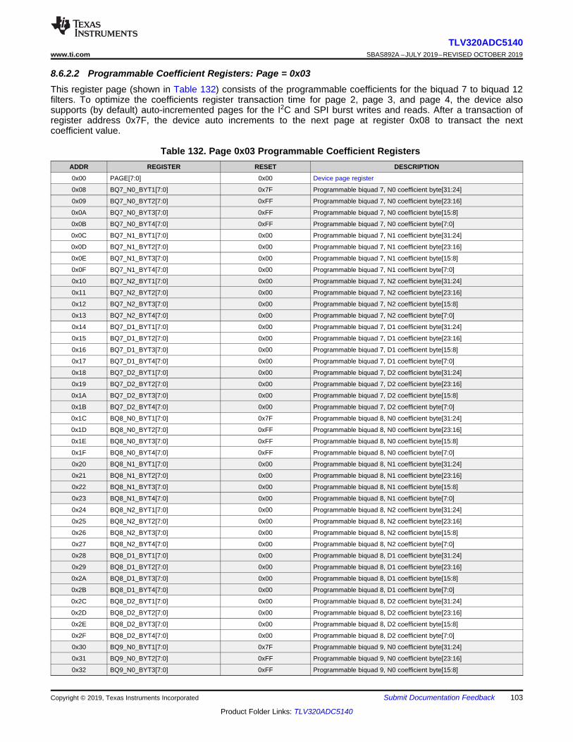
103
TLV320ADC5140www.ti.com SBAS892A –JULY 2019–REVISED OCTOBER 2019
Product Folder Links: TLV320ADC5140
Submit Documentation FeedbackCopyright © 2019, Texas Instruments Incorporated
8.6.2.2 Programmable Coefficient Registers: Page = 0x03This register page (shown in Table 132) consists of the programmable coefficients for the biquad 7 to biquad 12filters. To optimize the coefficients register transaction time for page 2, page 3, and page 4, the device alsosupports (by default) auto-incremented pages for the I2C and SPI burst writes and reads. After a transaction ofregister address 0x7F, the device auto increments to the next page at register 0x08 to transact the nextcoefficient value.
Table 132. Page 0x03 Programmable Coefficient RegistersADDR REGISTER RESET DESCRIPTION
0x00 PAGE[7:0] 0x00 Device page register
0x08 BQ7_N0_BYT1[7:0] 0x7F Programmable biquad 7, N0 coefficient byte[31:24]
0x09 BQ7_N0_BYT2[7:0] 0xFF Programmable biquad 7, N0 coefficient byte[23:16]
0x0A BQ7_N0_BYT3[7:0] 0xFF Programmable biquad 7, N0 coefficient byte[15:8]
0x0B BQ7_N0_BYT4[7:0] 0xFF Programmable biquad 7, N0 coefficient byte[7:0]
0x0C BQ7_N1_BYT1[7:0] 0x00 Programmable biquad 7, N1 coefficient byte[31:24]
0x0D BQ7_N1_BYT2[7:0] 0x00 Programmable biquad 7, N1 coefficient byte[23:16]
0x0E BQ7_N1_BYT3[7:0] 0x00 Programmable biquad 7, N1 coefficient byte[15:8]
0x0F BQ7_N1_BYT4[7:0] 0x00 Programmable biquad 7, N1 coefficient byte[7:0]
0x10 BQ7_N2_BYT1[7:0] 0x00 Programmable biquad 7, N2 coefficient byte[31:24]
0x11 BQ7_N2_BYT2[7:0] 0x00 Programmable biquad 7, N2 coefficient byte[23:16]
0x12 BQ7_N2_BYT3[7:0] 0x00 Programmable biquad 7, N2 coefficient byte[15:8]
0x13 BQ7_N2_BYT4[7:0] 0x00 Programmable biquad 7, N2 coefficient byte[7:0]
0x14 BQ7_D1_BYT1[7:0] 0x00 Programmable biquad 7, D1 coefficient byte[31:24]
0x15 BQ7_D1_BYT2[7:0] 0x00 Programmable biquad 7, D1 coefficient byte[23:16]
0x16 BQ7_D1_BYT3[7:0] 0x00 Programmable biquad 7, D1 coefficient byte[15:8]
0x17 BQ7_D1_BYT4[7:0] 0x00 Programmable biquad 7, D1 coefficient byte[7:0]
0x18 BQ7_D2_BYT1[7:0] 0x00 Programmable biquad 7, D2 coefficient byte[31:24]
0x19 BQ7_D2_BYT2[7:0] 0x00 Programmable biquad 7, D2 coefficient byte[23:16]
0x1A BQ7_D2_BYT3[7:0] 0x00 Programmable biquad 7, D2 coefficient byte[15:8]
0x1B BQ7_D2_BYT4[7:0] 0x00 Programmable biquad 7, D2 coefficient byte[7:0]
0x1C BQ8_N0_BYT1[7:0] 0x7F Programmable biquad 8, N0 coefficient byte[31:24]
0x1D BQ8_N0_BYT2[7:0] 0xFF Programmable biquad 8, N0 coefficient byte[23:16]
0x1E BQ8_N0_BYT3[7:0] 0xFF Programmable biquad 8, N0 coefficient byte[15:8]
0x1F BQ8_N0_BYT4[7:0] 0xFF Programmable biquad 8, N0 coefficient byte[7:0]
0x20 BQ8_N1_BYT1[7:0] 0x00 Programmable biquad 8, N1 coefficient byte[31:24]
0x21 BQ8_N1_BYT2[7:0] 0x00 Programmable biquad 8, N1 coefficient byte[23:16]
0x22 BQ8_N1_BYT3[7:0] 0x00 Programmable biquad 8, N1 coefficient byte[15:8]
0x23 BQ8_N1_BYT4[7:0] 0x00 Programmable biquad 8, N1 coefficient byte[7:0]
0x24 BQ8_N2_BYT1[7:0] 0x00 Programmable biquad 8, N2 coefficient byte[31:24]
0x25 BQ8_N2_BYT2[7:0] 0x00 Programmable biquad 8, N2 coefficient byte[23:16]
0x26 BQ8_N2_BYT3[7:0] 0x00 Programmable biquad 8, N2 coefficient byte[15:8]
0x27 BQ8_N2_BYT4[7:0] 0x00 Programmable biquad 8, N2 coefficient byte[7:0]
0x28 BQ8_D1_BYT1[7:0] 0x00 Programmable biquad 8, D1 coefficient byte[31:24]
0x29 BQ8_D1_BYT2[7:0] 0x00 Programmable biquad 8, D1 coefficient byte[23:16]
0x2A BQ8_D1_BYT3[7:0] 0x00 Programmable biquad 8, D1 coefficient byte[15:8]
0x2B BQ8_D1_BYT4[7:0] 0x00 Programmable biquad 8, D1 coefficient byte[7:0]
0x2C BQ8_D2_BYT1[7:0] 0x00 Programmable biquad 8, D2 coefficient byte[31:24]
0x2D BQ8_D2_BYT2[7:0] 0x00 Programmable biquad 8, D2 coefficient byte[23:16]
0x2E BQ8_D2_BYT3[7:0] 0x00 Programmable biquad 8, D2 coefficient byte[15:8]
0x2F BQ8_D2_BYT4[7:0] 0x00 Programmable biquad 8, D2 coefficient byte[7:0]
0x30 BQ9_N0_BYT1[7:0] 0x7F Programmable biquad 9, N0 coefficient byte[31:24]
0x31 BQ9_N0_BYT2[7:0] 0xFF Programmable biquad 9, N0 coefficient byte[23:16]
0x32 BQ9_N0_BYT3[7:0] 0xFF Programmable biquad 9, N0 coefficient byte[15:8]
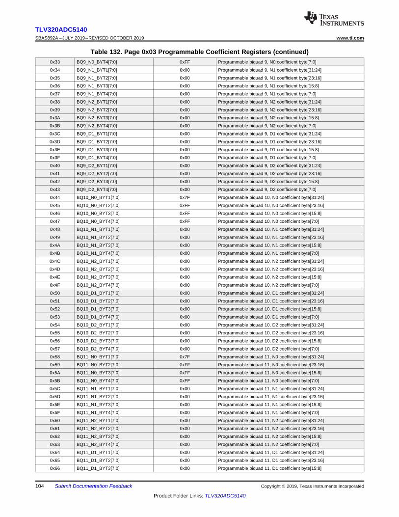
104
TLV320ADC5140SBAS892A –JULY 2019–REVISED OCTOBER 2019 www.ti.com
Product Folder Links: TLV320ADC5140
Submit Documentation Feedback Copyright © 2019, Texas Instruments Incorporated
Table 132. Page 0x03 Programmable Coefficient Registers (continued)0x33 BQ9_N0_BYT4[7:0] 0xFF Programmable biquad 9, N0 coefficient byte[7:0]
0x34 BQ9_N1_BYT1[7:0] 0x00 Programmable biquad 9, N1 coefficient byte[31:24]
0x35 BQ9_N1_BYT2[7:0] 0x00 Programmable biquad 9, N1 coefficient byte[23:16]
0x36 BQ9_N1_BYT3[7:0] 0x00 Programmable biquad 9, N1 coefficient byte[15:8]
0x37 BQ9_N1_BYT4[7:0] 0x00 Programmable biquad 9, N1 coefficient byte[7:0]
0x38 BQ9_N2_BYT1[7:0] 0x00 Programmable biquad 9, N2 coefficient byte[31:24]
0x39 BQ9_N2_BYT2[7:0] 0x00 Programmable biquad 9, N2 coefficient byte[23:16]
0x3A BQ9_N2_BYT3[7:0] 0x00 Programmable biquad 9, N2 coefficient byte[15:8]
0x3B BQ9_N2_BYT4[7:0] 0x00 Programmable biquad 9, N2 coefficient byte[7:0]
0x3C BQ9_D1_BYT1[7:0] 0x00 Programmable biquad 9, D1 coefficient byte[31:24]
0x3D BQ9_D1_BYT2[7:0] 0x00 Programmable biquad 9, D1 coefficient byte[23:16]
0x3E BQ9_D1_BYT3[7:0] 0x00 Programmable biquad 9, D1 coefficient byte[15:8]
0x3F BQ9_D1_BYT4[7:0] 0x00 Programmable biquad 9, D1 coefficient byte[7:0]
0x40 BQ9_D2_BYT1[7:0] 0x00 Programmable biquad 9, D2 coefficient byte[31:24]
0x41 BQ9_D2_BYT2[7:0] 0x00 Programmable biquad 9, D2 coefficient byte[23:16]
0x42 BQ9_D2_BYT3[7:0] 0x00 Programmable biquad 9, D2 coefficient byte[15:8]
0x43 BQ9_D2_BYT4[7:0] 0x00 Programmable biquad 9, D2 coefficient byte[7:0]
0x44 BQ10_N0_BYT1[7:0] 0x7F Programmable biquad 10, N0 coefficient byte[31:24]
0x45 BQ10_N0_BYT2[7:0] 0xFF Programmable biquad 10, N0 coefficient byte[23:16]
0x46 BQ10_N0_BYT3[7:0] 0xFF Programmable biquad 10, N0 coefficient byte[15:8]
0x47 BQ10_N0_BYT4[7:0] 0xFF Programmable biquad 10, N0 coefficient byte[7:0]
0x48 BQ10_N1_BYT1[7:0] 0x00 Programmable biquad 10, N1 coefficient byte[31:24]
0x49 BQ10_N1_BYT2[7:0] 0x00 Programmable biquad 10, N1 coefficient byte[23:16]
0x4A BQ10_N1_BYT3[7:0] 0x00 Programmable biquad 10, N1 coefficient byte[15:8]
0x4B BQ10_N1_BYT4[7:0] 0x00 Programmable biquad 10, N1 coefficient byte[7:0]
0x4C BQ10_N2_BYT1[7:0] 0x00 Programmable biquad 10, N2 coefficient byte[31:24]
0x4D BQ10_N2_BYT2[7:0] 0x00 Programmable biquad 10, N2 coefficient byte[23:16]
0x4E BQ10_N2_BYT3[7:0] 0x00 Programmable biquad 10, N2 coefficient byte[15:8]
0x4F BQ10_N2_BYT4[7:0] 0x00 Programmable biquad 10, N2 coefficient byte[7:0]
0x50 BQ10_D1_BYT1[7:0] 0x00 Programmable biquad 10, D1 coefficient byte[31:24]
0x51 BQ10_D1_BYT2[7:0] 0x00 Programmable biquad 10, D1 coefficient byte[23:16]
0x52 BQ10_D1_BYT3[7:0] 0x00 Programmable biquad 10, D1 coefficient byte[15:8]
0x53 BQ10_D1_BYT4[7:0] 0x00 Programmable biquad 10, D1 coefficient byte[7:0]
0x54 BQ10_D2_BYT1[7:0] 0x00 Programmable biquad 10, D2 coefficient byte[31:24]
0x55 BQ10_D2_BYT2[7:0] 0x00 Programmable biquad 10, D2 coefficient byte[23:16]
0x56 BQ10_D2_BYT3[7:0] 0x00 Programmable biquad 10, D2 coefficient byte[15:8]
0x57 BQ10_D2_BYT4[7:0] 0x00 Programmable biquad 10, D2 coefficient byte[7:0]
0x58 BQ11_N0_BYT1[7:0] 0x7F Programmable biquad 11, N0 coefficient byte[31:24]
0x59 BQ11_N0_BYT2[7:0] 0xFF Programmable biquad 11, N0 coefficient byte[23:16]
0x5A BQ11_N0_BYT3[7:0] 0xFF Programmable biquad 11, N0 coefficient byte[15:8]
0x5B BQ11_N0_BYT4[7:0] 0xFF Programmable biquad 11, N0 coefficient byte[7:0]
0x5C BQ11_N1_BYT1[7:0] 0x00 Programmable biquad 11, N1 coefficient byte[31:24]
0x5D BQ11_N1_BYT2[7:0] 0x00 Programmable biquad 11, N1 coefficient byte[23:16]
0x5E BQ11_N1_BYT3[7:0] 0x00 Programmable biquad 11, N1 coefficient byte[15:8]
0x5F BQ11_N1_BYT4[7:0] 0x00 Programmable biquad 11, N1 coefficient byte[7:0]
0x60 BQ11_N2_BYT1[7:0] 0x00 Programmable biquad 11, N2 coefficient byte[31:24]
0x61 BQ11_N2_BYT2[7:0] 0x00 Programmable biquad 11, N2 coefficient byte[23:16]
0x62 BQ11_N2_BYT3[7:0] 0x00 Programmable biquad 11, N2 coefficient byte[15:8]
0x63 BQ11_N2_BYT4[7:0] 0x00 Programmable biquad 11, N2 coefficient byte[7:0]
0x64 BQ11_D1_BYT1[7:0] 0x00 Programmable biquad 11, D1 coefficient byte[31:24]
0x65 BQ11_D1_BYT2[7:0] 0x00 Programmable biquad 11, D1 coefficient byte[23:16]
0x66 BQ11_D1_BYT3[7:0] 0x00 Programmable biquad 11, D1 coefficient byte[15:8]
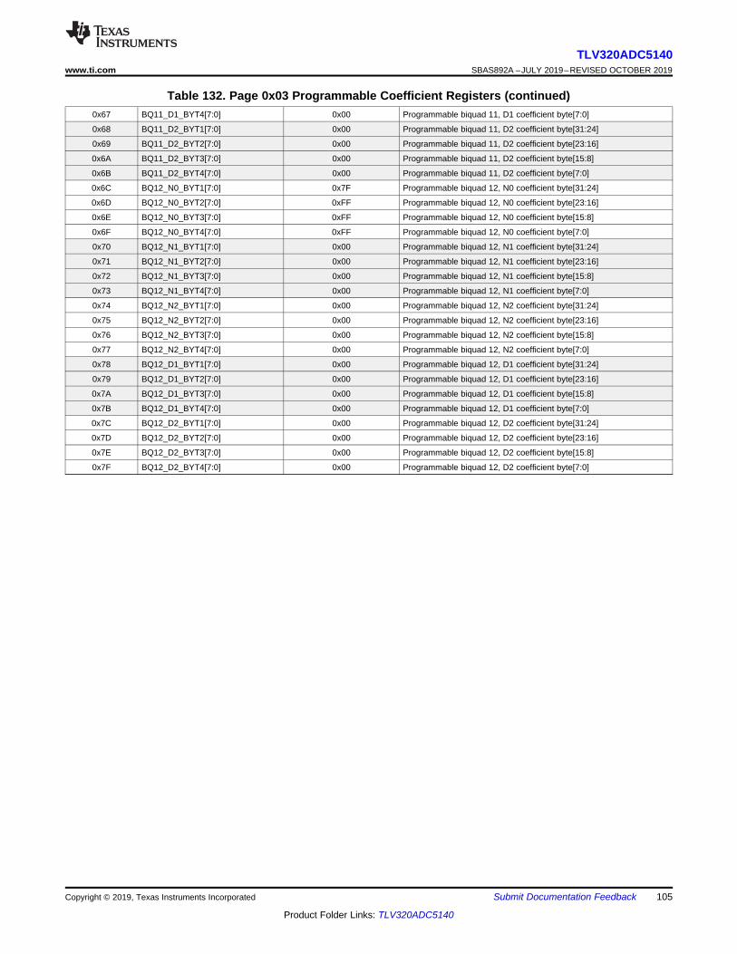
105
TLV320ADC5140www.ti.com SBAS892A –JULY 2019–REVISED OCTOBER 2019
Product Folder Links: TLV320ADC5140
Submit Documentation FeedbackCopyright © 2019, Texas Instruments Incorporated
Table 132. Page 0x03 Programmable Coefficient Registers (continued)0x67 BQ11_D1_BYT4[7:0] 0x00 Programmable biquad 11, D1 coefficient byte[7:0]
0x68 BQ11_D2_BYT1[7:0] 0x00 Programmable biquad 11, D2 coefficient byte[31:24]
0x69 BQ11_D2_BYT2[7:0] 0x00 Programmable biquad 11, D2 coefficient byte[23:16]
0x6A BQ11_D2_BYT3[7:0] 0x00 Programmable biquad 11, D2 coefficient byte[15:8]
0x6B BQ11_D2_BYT4[7:0] 0x00 Programmable biquad 11, D2 coefficient byte[7:0]
0x6C BQ12_N0_BYT1[7:0] 0x7F Programmable biquad 12, N0 coefficient byte[31:24]
0x6D BQ12_N0_BYT2[7:0] 0xFF Programmable biquad 12, N0 coefficient byte[23:16]
0x6E BQ12_N0_BYT3[7:0] 0xFF Programmable biquad 12, N0 coefficient byte[15:8]
0x6F BQ12_N0_BYT4[7:0] 0xFF Programmable biquad 12, N0 coefficient byte[7:0]
0x70 BQ12_N1_BYT1[7:0] 0x00 Programmable biquad 12, N1 coefficient byte[31:24]
0x71 BQ12_N1_BYT2[7:0] 0x00 Programmable biquad 12, N1 coefficient byte[23:16]
0x72 BQ12_N1_BYT3[7:0] 0x00 Programmable biquad 12, N1 coefficient byte[15:8]
0x73 BQ12_N1_BYT4[7:0] 0x00 Programmable biquad 12, N1 coefficient byte[7:0]
0x74 BQ12_N2_BYT1[7:0] 0x00 Programmable biquad 12, N2 coefficient byte[31:24]
0x75 BQ12_N2_BYT2[7:0] 0x00 Programmable biquad 12, N2 coefficient byte[23:16]
0x76 BQ12_N2_BYT3[7:0] 0x00 Programmable biquad 12, N2 coefficient byte[15:8]
0x77 BQ12_N2_BYT4[7:0] 0x00 Programmable biquad 12, N2 coefficient byte[7:0]
0x78 BQ12_D1_BYT1[7:0] 0x00 Programmable biquad 12, D1 coefficient byte[31:24]
0x79 BQ12_D1_BYT2[7:0] 0x00 Programmable biquad 12, D1 coefficient byte[23:16]
0x7A BQ12_D1_BYT3[7:0] 0x00 Programmable biquad 12, D1 coefficient byte[15:8]
0x7B BQ12_D1_BYT4[7:0] 0x00 Programmable biquad 12, D1 coefficient byte[7:0]
0x7C BQ12_D2_BYT1[7:0] 0x00 Programmable biquad 12, D2 coefficient byte[31:24]
0x7D BQ12_D2_BYT2[7:0] 0x00 Programmable biquad 12, D2 coefficient byte[23:16]
0x7E BQ12_D2_BYT3[7:0] 0x00 Programmable biquad 12, D2 coefficient byte[15:8]
0x7F BQ12_D2_BYT4[7:0] 0x00 Programmable biquad 12, D2 coefficient byte[7:0]
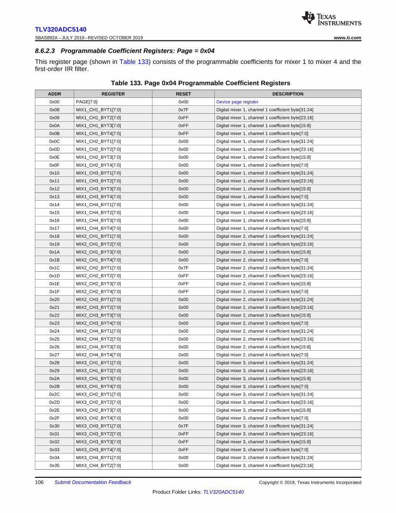
106
TLV320ADC5140SBAS892A –JULY 2019–REVISED OCTOBER 2019 www.ti.com
Product Folder Links: TLV320ADC5140
Submit Documentation Feedback Copyright © 2019, Texas Instruments Incorporated
8.6.2.3 Programmable Coefficient Registers: Page = 0x04This register page (shown in Table 133) consists of the programmable coefficients for mixer 1 to mixer 4 and thefirst-order IIR filter.
Table 133. Page 0x04 Programmable Coefficient RegistersADDR REGISTER RESET DESCRIPTION
0x00 PAGE[7:0] 0x00 Device page register
0x08 MIX1_CH1_BYT1[7:0] 0x7F Digital mixer 1, channel 1 coefficient byte[31:24]
0x09 MIX1_CH1_BYT2[7:0] 0xFF Digital mixer 1, channel 1 coefficient byte[23:16]
0x0A MIX1_CH1_BYT3[7:0] 0xFF Digital mixer 1, channel 1 coefficient byte[15:8]
0x0B MIX1_CH1_BYT4[7:0] 0xFF Digital mixer 1, channel 1 coefficient byte[7:0]
0x0C MIX1_CH2_BYT1[7:0] 0x00 Digital mixer 1, channel 2 coefficient byte[31:24]
0x0D MIX1_CH2_BYT2[7:0] 0x00 Digital mixer 1, channel 2 coefficient byte[23:16]
0x0E MIX1_CH2_BYT3[7:0] 0x00 Digital mixer 1, channel 2 coefficient byte[15:8]
0x0F MIX1_CH2_BYT4[7:0] 0x00 Digital mixer 1, channel 2 coefficient byte[7:0]
0x10 MIX1_CH3_BYT1[7:0] 0x00 Digital mixer 1, channel 3 coefficient byte[31:24]
0x11 MIX1_CH3_BYT2[7:0] 0x00 Digital mixer 1, channel 3 coefficient byte[23:16]
0x12 MIX1_CH3_BYT3[7:0] 0x00 Digital mixer 1, channel 3 coefficient byte[15:8]
0x13 MIX1_CH3_BYT4[7:0] 0x00 Digital mixer 1, channel 3 coefficient byte[7:0]
0x14 MIX1_CH4_BYT1[7:0] 0x00 Digital mixer 1, channel 4 coefficient byte[31:24]
0x15 MIX1_CH4_BYT2[7:0] 0x00 Digital mixer 1, channel 4 coefficient byte[23:16]
0x16 MIX1_CH4_BYT3[7:0] 0x00 Digital mixer 1, channel 4 coefficient byte[15:8]
0x17 MIX1_CH4_BYT4[7:0] 0x00 Digital mixer 1, channel 4 coefficient byte[7:0]
0x18 MIX2_CH1_BYT1[7:0] 0x00 Digital mixer 2, channel 1 coefficient byte[31:24]
0x19 MIX2_CH1_BYT2[7:0] 0x00 Digital mixer 2, channel 1 coefficient byte[23:16]
0x1A MIX2_CH1_BYT3[7:0] 0x00 Digital mixer 2, channel 1 coefficient byte[15:8]
0x1B MIX2_CH1_BYT4[7:0] 0x00 Digital mixer 2, channel 1 coefficient byte[7:0]
0x1C MIX2_CH2_BYT1[7:0] 0x7F Digital mixer 2, channel 2 coefficient byte[31:24]
0x1D MIX2_CH2_BYT2[7:0] 0xFF Digital mixer 2, channel 2 coefficient byte[23:16]
0x1E MIX2_CH2_BYT3[7:0] 0xFF Digital mixer 2, channel 2 coefficient byte[15:8]
0x1F MIX2_CH2_BYT4[7:0] 0xFF Digital mixer 2, channel 2 coefficient byte[7:0]
0x20 MIX2_CH3_BYT1[7:0] 0x00 Digital mixer 2, channel 3 coefficient byte[31:24]
0x21 MIX2_CH3_BYT2[7:0] 0x00 Digital mixer 2, channel 3 coefficient byte[23:16]
0x22 MIX2_CH3_BYT3[7:0] 0x00 Digital mixer 2, channel 3 coefficient byte[15:8]
0x23 MIX2_CH3_BYT4[7:0] 0x00 Digital mixer 2, channel 3 coefficient byte[7:0]
0x24 MIX2_CH4_BYT1[7:0] 0x00 Digital mixer 2, channel 4 coefficient byte[31:24]
0x25 MIX2_CH4_BYT2[7:0] 0x00 Digital mixer 2, channel 4 coefficient byte[23:16]
0x26 MIX2_CH4_BYT3[7:0] 0x00 Digital mixer 2, channel 4 coefficient byte[15:8]
0x27 MIX2_CH4_BYT4[7:0] 0x00 Digital mixer 2, channel 4 coefficient byte[7:0]
0x28 MIX3_CH1_BYT1[7:0] 0x00 Digital mixer 3, channel 1 coefficient byte[31:24]
0x29 MIX3_CH1_BYT2[7:0] 0x00 Digital mixer 3, channel 1 coefficient byte[23:16]
0x2A MIX3_CH1_BYT3[7:0] 0x00 Digital mixer 3, channel 1 coefficient byte[15:8]
0x2B MIX3_CH1_BYT4[7:0] 0x00 Digital mixer 3, channel 1 coefficient byte[7:0]
0x2C MIX3_CH2_BYT1[7:0] 0x00 Digital mixer 3, channel 2 coefficient byte[31:24]
0x2D MIX3_CH2_BYT2[7:0] 0x00 Digital mixer 3, channel 2 coefficient byte[23:16]
0x2E MIX3_CH2_BYT3[7:0] 0x00 Digital mixer 3, channel 2 coefficient byte[15:8]
0x2F MIX3_CH2_BYT4[7:0] 0x00 Digital mixer 3, channel 2 coefficient byte[7:0]
0x30 MIX3_CH3_BYT1[7:0] 0x7F Digital mixer 3, channel 3 coefficient byte[31:24]
0x31 MIX3_CH3_BYT2[7:0] 0xFF Digital mixer 3, channel 3 coefficient byte[23:16]
0x32 MIX3_CH3_BYT3[7:0] 0xFF Digital mixer 3, channel 3 coefficient byte[15:8]
0x33 MIX3_CH3_BYT4[7:0] 0xFF Digital mixer 3, channel 3 coefficient byte[7:0]
0x34 MIX3_CH4_BYT1[7:0] 0x00 Digital mixer 3, channel 4 coefficient byte[31:24]
0x35 MIX3_CH4_BYT2[7:0] 0x00 Digital mixer 3, channel 4 coefficient byte[23:16]
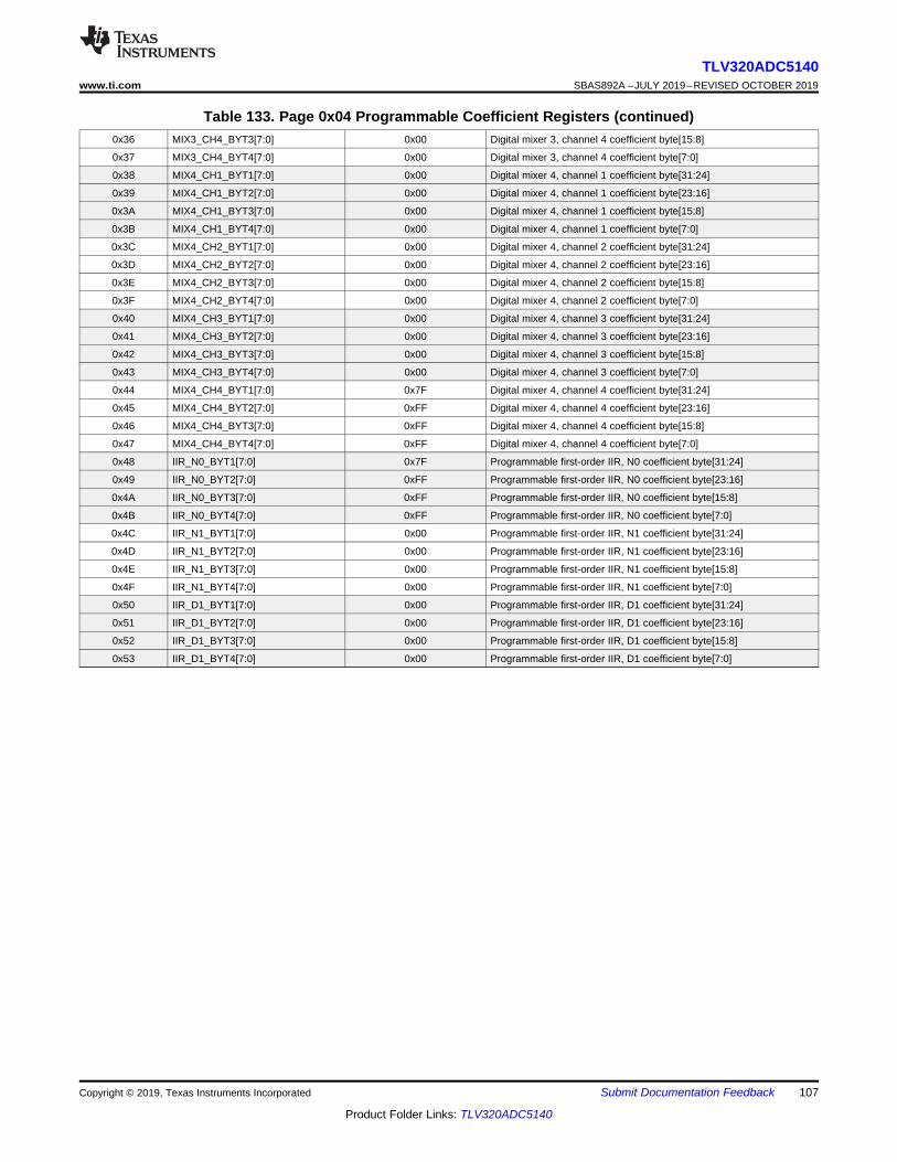
107
TLV320ADC5140www.ti.com SBAS892A –JULY 2019–REVISED OCTOBER 2019
Product Folder Links: TLV320ADC5140
Submit Documentation FeedbackCopyright © 2019, Texas Instruments Incorporated
Table 133. Page 0x04 Programmable Coefficient Registers (continued)0x36 MIX3_CH4_BYT3[7:0] 0x00 Digital mixer 3, channel 4 coefficient byte[15:8]
0x37 MIX3_CH4_BYT4[7:0] 0x00 Digital mixer 3, channel 4 coefficient byte[7:0]
0x38 MIX4_CH1_BYT1[7:0] 0x00 Digital mixer 4, channel 1 coefficient byte[31:24]
0x39 MIX4_CH1_BYT2[7:0] 0x00 Digital mixer 4, channel 1 coefficient byte[23:16]
0x3A MIX4_CH1_BYT3[7:0] 0x00 Digital mixer 4, channel 1 coefficient byte[15:8]
0x3B MIX4_CH1_BYT4[7:0] 0x00 Digital mixer 4, channel 1 coefficient byte[7:0]
0x3C MIX4_CH2_BYT1[7:0] 0x00 Digital mixer 4, channel 2 coefficient byte[31:24]
0x3D MIX4_CH2_BYT2[7:0] 0x00 Digital mixer 4, channel 2 coefficient byte[23:16]
0x3E MIX4_CH2_BYT3[7:0] 0x00 Digital mixer 4, channel 2 coefficient byte[15:8]
0x3F MIX4_CH2_BYT4[7:0] 0x00 Digital mixer 4, channel 2 coefficient byte[7:0]
0x40 MIX4_CH3_BYT1[7:0] 0x00 Digital mixer 4, channel 3 coefficient byte[31:24]
0x41 MIX4_CH3_BYT2[7:0] 0x00 Digital mixer 4, channel 3 coefficient byte[23:16]
0x42 MIX4_CH3_BYT3[7:0] 0x00 Digital mixer 4, channel 3 coefficient byte[15:8]
0x43 MIX4_CH3_BYT4[7:0] 0x00 Digital mixer 4, channel 3 coefficient byte[7:0]
0x44 MIX4_CH4_BYT1[7:0] 0x7F Digital mixer 4, channel 4 coefficient byte[31:24]
0x45 MIX4_CH4_BYT2[7:0] 0xFF Digital mixer 4, channel 4 coefficient byte[23:16]
0x46 MIX4_CH4_BYT3[7:0] 0xFF Digital mixer 4, channel 4 coefficient byte[15:8]
0x47 MIX4_CH4_BYT4[7:0] 0xFF Digital mixer 4, channel 4 coefficient byte[7:0]
0x48 IIR_N0_BYT1[7:0] 0x7F Programmable first-order IIR, N0 coefficient byte[31:24]
0x49 IIR_N0_BYT2[7:0] 0xFF Programmable first-order IIR, N0 coefficient byte[23:16]
0x4A IIR_N0_BYT3[7:0] 0xFF Programmable first-order IIR, N0 coefficient byte[15:8]
0x4B IIR_N0_BYT4[7:0] 0xFF Programmable first-order IIR, N0 coefficient byte[7:0]
0x4C IIR_N1_BYT1[7:0] 0x00 Programmable first-order IIR, N1 coefficient byte[31:24]
0x4D IIR_N1_BYT2[7:0] 0x00 Programmable first-order IIR, N1 coefficient byte[23:16]
0x4E IIR_N1_BYT3[7:0] 0x00 Programmable first-order IIR, N1 coefficient byte[15:8]
0x4F IIR_N1_BYT4[7:0] 0x00 Programmable first-order IIR, N1 coefficient byte[7:0]
0x50 IIR_D1_BYT1[7:0] 0x00 Programmable first-order IIR, D1 coefficient byte[31:24]
0x51 IIR_D1_BYT2[7:0] 0x00 Programmable first-order IIR, D1 coefficient byte[23:16]
0x52 IIR_D1_BYT3[7:0] 0x00 Programmable first-order IIR, D1 coefficient byte[15:8]
0x53 IIR_D1_BYT4[7:0] 0x00 Programmable first-order IIR, D1 coefficient byte[7:0]
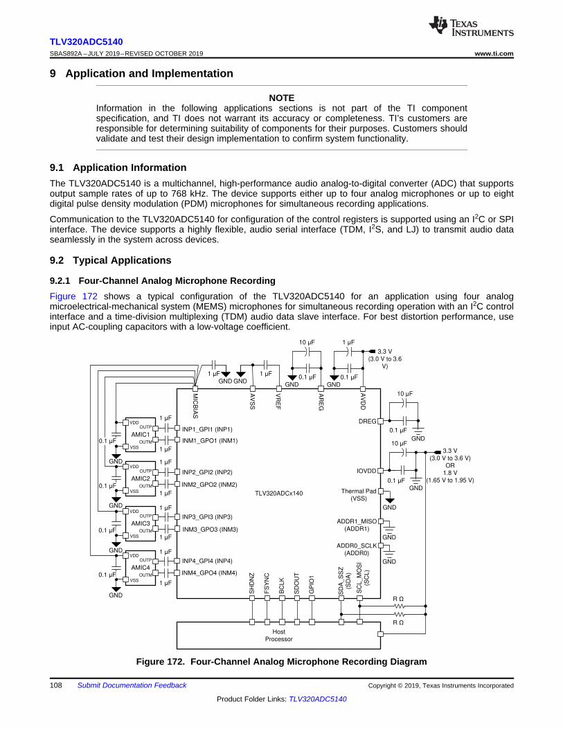
1 F
1 F
1 F
1 F
1 F
1 F
1 F
1 F
3.3 V
(3.0 V to 3.6 V)
OR
1.8 V
(1.65 V to 1.95 V)
3.3 V
(3.0 V to 3.6
V)
TLV320ADCx140
INP1_GPI1 (INP1)
INM1_GPO1 (INM1)
GND
GND
GND
GND
MIC
BIA
S
AV
SS
VR
EF
GND
1 F
AR
EG
0.1 F
GND
1 F
GND
10 F
AV
DD
1 F
DREG
10 F
GND
0.1 F
0.1 F
INP2_GPI2 (INP2)
INM2_GPO2 (INM2)
INP3_GPI3 (INP3)
INM3_GPO3 (INM3)
INP4_GPI4 (INP4)
INM4_GPO4 (INM4)
Host
Processor
IOVDD
GND
Thermal Pad
(VSS)
GND
ADDR1_MISO
(ADDR1)
GND
ADDR0_SCLK
(ADDR0)
GND
SC
L_M
OS
I
(SC
L)
SD
A_
SS
Z
(SD
A)
R
R
GP
IO1
SD
OU
T
BC
LK
FS
YN
C
SH
DN
Z
10 F
AMIC1
OUTP
OUTM
VDD
VSS
AMIC2
OUTP
OUTM
VDD
VSS
AMIC3
OUTP
OUTM
VDD
VSS
AMIC4
OUTP
OUTM
VDD
VSS
GND
0.1 F
0.1 F
0.1 F
0.1 F
0.1 F
108
TLV320ADC5140SBAS892A –JULY 2019–REVISED OCTOBER 2019 www.ti.com
Product Folder Links: TLV320ADC5140
Submit Documentation Feedback Copyright © 2019, Texas Instruments Incorporated
9 Application and Implementation
NOTEInformation in the following applications sections is not part of the TI componentspecification, and TI does not warrant its accuracy or completeness. TI’s customers areresponsible for determining suitability of components for their purposes. Customers shouldvalidate and test their design implementation to confirm system functionality.
9.1 Application InformationThe TLV320ADC5140 is a multichannel, high-performance audio analog-to-digital converter (ADC) that supportsoutput sample rates of up to 768 kHz. The device supports either up to four analog microphones or up to eightdigital pulse density modulation (PDM) microphones for simultaneous recording applications.
Communication to the TLV320ADC5140 for configuration of the control registers is supported using an I2C or SPIinterface. The device supports a highly flexible, audio serial interface (TDM, I2S, and LJ) to transmit audio dataseamlessly in the system across devices.
9.2 Typical Applications
9.2.1 Four-Channel Analog Microphone RecordingFigure 172 shows a typical configuration of the TLV320ADC5140 for an application using four analogmicroelectrical-mechanical system (MEMS) microphones for simultaneous recording operation with an I2C controlinterface and a time-division multiplexing (TDM) audio data slave interface. For best distortion performance, useinput AC-coupling capacitors with a low-voltage coefficient.
Figure 172. Four-Channel Analog Microphone Recording Diagram
109
TLV320ADC5140www.ti.com SBAS892A –JULY 2019–REVISED OCTOBER 2019
Product Folder Links: TLV320ADC5140
Submit Documentation FeedbackCopyright © 2019, Texas Instruments Incorporated
Typical Applications (continued)9.2.1.1 Design RequirementsTable 134 lists the design parameters for this application.
Table 134. Design ParametersKEY PARAMETER SPECIFICATION
AVDD 3.3 VAVDD supply current consumption > 23 mA (PLL on, four-channel recording, fS = 48 kHz)IOVDD 1.8 V or 3.3 VMaximum MICBIAS current 10 mA (MICBIAS voltage is the same as AVDD)
9.2.1.2 Detailed Design ProcedureThis section describes the necessary steps to configure the TLV320ADC5140 for this specific application. Thefollowing steps provide a sequence of items that must be executed in the time between powering the device upand reading data from the device or transitioning from one mode to another mode of operation.1. Apply power to the device:
a. Power-up the IOVDD and AVDD power supplies, keeping the SHDNZ pin voltage lowb. The device now goes into hardware shutdown mode (ultra-low-power mode < 1 µA)
2. Transition from hardware shutdown mode to sleep mode (or software shutdown mode):a. Release SHDNZ only when the IOVDD and AVDD power supplies settle to the steady-state operating
voltageb. Wait for at least 1 ms to allow the device to initialize the internal registersc. The device now goes into sleep mode (low-power mode < 10 µA)
3. Transition from sleep mode to active mode whenever required for the recording operation:a. Wake up the device by writing to P0_R2 to disable sleep modeb. Wait for at least 1 ms to allow the device to complete the internal wake-up sequencec. Override default configuration registers or programmable coefficients value as required (this step is
optional)d. Enable all desired input channels by writing to P0_R115e. Enable all desired audio serial interface output channels by writing to P0_R116f. Power-up the ADC, MICBIAS, and PLL by writing to P0_R117g. Apply FSYNC and BCLK with the desired output sample rates and the BCLK to FSYNC ratio
This specific step can be done at any point in the sequence after step a.
See the Phase-Locked Loop (PLL) and Clock Generation section for supported sample rates and theBCLK to FSYNC ratio.
h. The device recording data are now sent to the host processor via the TDM audio serial data bus4. Transition from active mode to sleep mode (again) as required in the system for low-power operation:
a. Enter sleep mode by writing to P0_R2 to enable sleep modeb. Wait at least 6 ms (when FSYNC = 48 kHz) for the volume to ramp down and for all blocks to power
downc. Read P0_R119 to check the device shutdown and sleep mode statusd. If the device P0_R119_D7 status bit is 1'b1 then stop FSYNC and BCLK in the systeme. The device now goes into sleep mode (low-power mode < 10 µA) and retains all register values
5. Transition from sleep mode to active mode (again) as required for the recording operation:a. Wake up the device by writing to P0_R2 to disable sleep modeb. Wait for at least 1 ms to allow the device to complete the internal wake-up sequencec. Apply FSYNC and BCLK with the desired output sample rates and the BCLK to FSYNC ratiod. The device recording data are now sent to the host processor via the TDM audio serial data bus

110
TLV320ADC5140SBAS892A –JULY 2019–REVISED OCTOBER 2019 www.ti.com
Product Folder Links: TLV320ADC5140
Submit Documentation Feedback Copyright © 2019, Texas Instruments Incorporated
6. Repeat step 4 and step 5 as required for mode transitions7. Assert the SHDNZ pin low to enter hardware shutdown mode (again) at any time8. Follow step 2 onwards to exit hardware shutdown mode (again)
9.2.1.2.1 Example Device Register Configuration Script for EVM Setup
This section provides a typical EVM I2C register control script that shows how to set up the TLV320ADC5140 in afour-channel analog microphone recording mode with differential inputs.
# Key: w 98 XX YY ==> write to I2C address 0x98, to register 0xXX, data 0xYY# # ==> comment delimiter## The following list gives an example sequence of items that must be executed in the time# between powering the device up and reading data from the device. Note that there are# other valid sequences depending on which features are used.## See the TLV320ADC5140EVM user guide for jumper settings and audio connections.## Differential 4-channel : INP1/INM1 - Ch1, INP2/INM2 - Ch2, INP3/INM3 - Ch3 and INP4/INM4 - Ch4# FSYNC = 44.1 kHz (Output Data Sample Rate), BCLK = 11.2896 MHz (BCLK/FSYNC = 256)################################################################### Power up IOVDD and AVDD power supplies keeping SHDNZ pin voltage LOW# Wait for IOVDD and AVDD power supplies to settle to steady state operating voltage range.# Release SHDNZ to HIGH.# Wait for 1ms.## Wake-up device by I2C write into P0_R2 using internal AREGw 98 02 81## Enable Input Ch-1 to Ch-4 by I2C write into P0_R115w 98 73 F0## Enable ASI Output Ch-1 to Ch-4 slots by I2C write into P0_R116w 98 74 F0## Power-up ADC, MICBIAS and PLL by I2C write into P0_R117w 98 75 E0## Apply FSYNC = 44.1 kHz and BCLK = 11.2896 MHz and# Start recording data by host on ASI bus with TDM protocol 32-bits channel wordlength
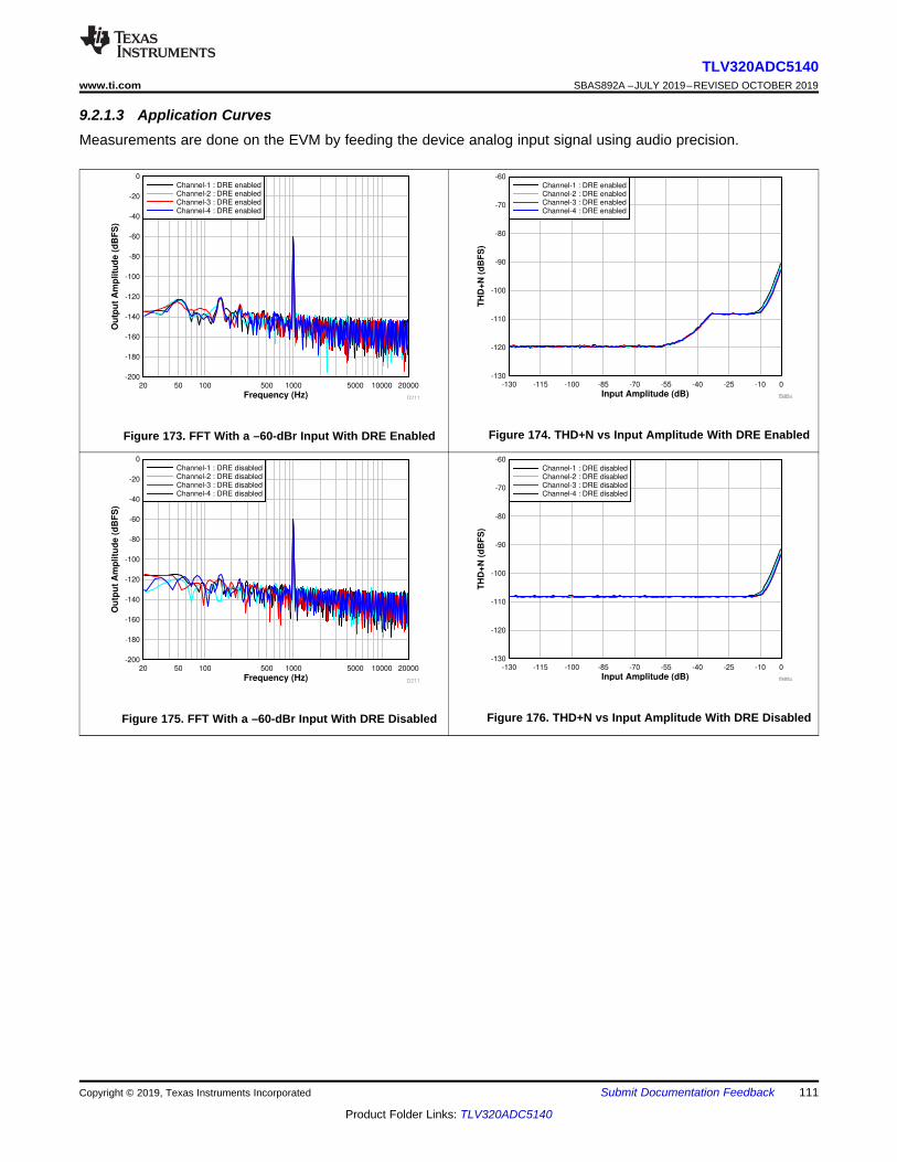
Frequency (Hz)
Ou
tpu
t A
mp
litu
de (
dB
FS
)
20 50 100 500 1000 5000 10000 20000
-200
-180
-160
-140
-120
-100
-80
-60
-40
-20
0
D211
Channel-1 : DRE disabled
Channel-2 : DRE disabled
Channel-3 : DRE disabled
Channel-4 : DRE disabled
Input Amplitude (dB)
TH
D+
N (
dB
FS
)
-130 -115 -100 -85 -70 -55 -40 -25 -10 0
-130
-120
-110
-100
-90
-80
-70
-60
THD+D201
Channel-1 : DRE disabled
Channel-2 : DRE disabled
Channel-3 : DRE disabled
Channel-4 : DRE disabled
Frequency (Hz)
Ou
tpu
t A
mp
litu
de (
dB
FS
)
20 50 100 500 1000 5000 10000 20000
-200
-180
-160
-140
-120
-100
-80
-60
-40
-20
0
D211
Channel-1 : DRE enabled
Channel-2 : DRE enabled
Channel-3 : DRE enabled
Channel-4 : DRE enabled
Input Amplitude (dB)
TH
D+
N (
dB
FS
)
-130 -115 -100 -85 -70 -55 -40 -25 -10 0
-130
-120
-110
-100
-90
-80
-70
-60
THD+D201
Channel-1 : DRE enabled
Channel-2 : DRE enabled
Channel-3 : DRE enabled
Channel-4 : DRE enabled
111
TLV320ADC5140www.ti.com SBAS892A –JULY 2019–REVISED OCTOBER 2019
Product Folder Links: TLV320ADC5140
Submit Documentation FeedbackCopyright © 2019, Texas Instruments Incorporated
9.2.1.3 Application CurvesMeasurements are done on the EVM by feeding the device analog input signal using audio precision.
Figure 173. FFT With a –60-dBr Input With DRE Enabled Figure 174. THD+N vs Input Amplitude With DRE Enabled
Figure 175. FFT With a –60-dBr Input With DRE Disabled Figure 176. THD+N vs Input Amplitude With DRE Disabled
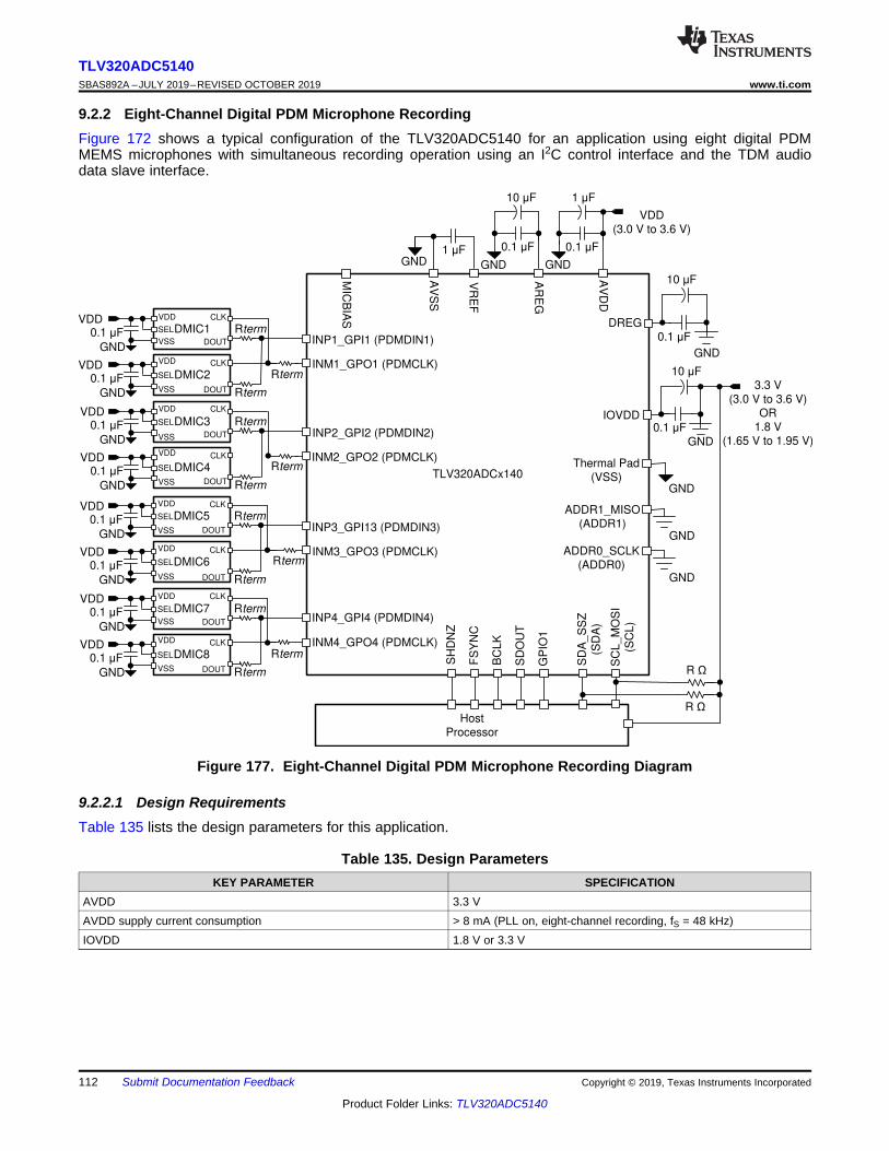
3.3 V
(3.0 V to 3.6 V)
OR
1.8 V
(1.65 V to 1.95 V)
0.1 F
TLV320ADCx140
DMIC1DOUT
CLKVDD
VSS INP1_GPI1 (PDMDIN1)
INM1_GPO1 (PDMCLK)
GND
MIC
BIA
S
Host
Processor
SC
L_M
OS
I
(SC
L)
SD
A_
SS
Z
(SD
A)
R
R
GP
IO1
SD
OU
T
BC
LK
FS
YN
C
SH
DN
Z
SEL Rterm
Rterm
INP2_GPI2 (PDMDIN2)
INM2_GPO2 (PDMCLK)Rterm
INP3_GPI13 (PDMDIN3)
INM3_GPO3 (PDMCLK)
INP4_GPI4 (PDMDIN4)
INM4_GPO4 (PDMCLK)
VDD
Rterm
Rterm
AV
SS
VR
EF
GND1 F
AR
EG
GND
10 F
AV
DD
1 F
0.1 F
GND
0.1 F
VDD
(3.0 V to 3.6 V)
Thermal Pad
(VSS)GND
ADDR1_MISO
(ADDR1)GND
ADDR0_SCLK
(ADDR0)GND
DREG
GND
IOVDD
GND
10 F
0.1 F
0.1 F
10 F
0.1 F DMIC2
DOUT
CLKVDD
VSSGND
SELVDD
Rterm
0.1 F DMIC3DOUT
CLKVDD
VSSGND
SEL RtermVDD
0.1 F DMIC4DOUT
CLKVDD
VSSGND
SELVDD
Rterm
0.1 F DMIC5DOUT
CLKVDD
VSSGND
SEL RtermVDD
0.1 F DMIC6
DOUT
CLKVDD
VSSGND
SELVDD
Rterm
0.1 F DMIC7DOUT
CLKVDD
VSSGND
SEL RtermVDD
0.1 F DMIC8
DOUT
CLKVDD
VSSGND
SELVDD
Rterm
112
TLV320ADC5140SBAS892A –JULY 2019–REVISED OCTOBER 2019 www.ti.com
Product Folder Links: TLV320ADC5140
Submit Documentation Feedback Copyright © 2019, Texas Instruments Incorporated
9.2.2 Eight-Channel Digital PDM Microphone RecordingFigure 172 shows a typical configuration of the TLV320ADC5140 for an application using eight digital PDMMEMS microphones with simultaneous recording operation using an I2C control interface and the TDM audiodata slave interface.
Figure 177. Eight-Channel Digital PDM Microphone Recording Diagram
9.2.2.1 Design RequirementsTable 135 lists the design parameters for this application.
Table 135. Design ParametersKEY PARAMETER SPECIFICATION
AVDD 3.3 VAVDD supply current consumption > 8 mA (PLL on, eight-channel recording, fS = 48 kHz)IOVDD 1.8 V or 3.3 V
113
TLV320ADC5140www.ti.com SBAS892A –JULY 2019–REVISED OCTOBER 2019
Product Folder Links: TLV320ADC5140
Submit Documentation FeedbackCopyright © 2019, Texas Instruments Incorporated
9.2.2.2 Detailed Design ProcedureThis section describes the necessary steps to configure the TLV320ADC5140 for this specific application. Thefollowing steps provide a sequence of items that must be executed in the time between powering the device upand reading data from the device or transitioning from one mode to another mode of operation.1. Apply power to the device:
a. Power up the IOVDD and AVDD power supplies, keeping the SHDNZ pin voltage lowb. The device now goes into hardware shutdown mode (ultra-low-power mode < 1 µA)
2. Transition from hardware shutdown mode to sleep mode (or software shutdown mode):a. Release SHDNZ only when the IOVDD and AVDD power supplies settle to the steady-state operating
voltageb. Wait for at least 1 ms to allow the device to initialize the internal registers initializationc. The device now goes into sleep mode (low-power mode < 10 µA)
3. Transition from sleep mode to active mode whenever required for the recording operation:a. Wake up the device by writing to P0_R2 to disable sleep modeb. Wait for at least 1 ms to allow the device to complete the internal wake-up sequencec. Override the default configuration registers or programmable coefficients value as required (this step is
optional)d. Configure channel 1 to channel 4 (CHx_INSRC) for the digital microphone as the input source for
recordinge. Configure GPO1 to GPO4 (GPOx_CFG) as the PDMCLK outputf. Configure GPI1 to GPI4 (GPI1x_CFG) as PDMDIN1 to PDMDIN4, respectivelyg. Enable all desired input channels by writing to P0_R115h. Enable all desired audio serial interface output channels by writing to P0_R116i. Power-up the ADC and PLL by writing to P0_R117j. Apply FSYNC and BCLK with the desired output sample rates and the BCLK to FSYNC ratio
This specific step can be done at any point in the sequence after step a.
See the Phase-Locked Loop (PLL) and Clock Generation section for supported sample rates and theBCLK to FSYNC ratio.
k. The device recording data is now sent to the host processor using the TDM audio serial data bus4. Transition from active mode to sleep mode (again) as required in the system for low-power operation:
a. Enter sleep mode by writing to P0_R2 to enable sleep modeb. Wait at least 6 ms (when FSYNC = 48 kHz) for the volume to ramp down and for all blocks to power
downc. Read P0_R119 to check the device shutdown and sleep mode statusd. If the device P0_R119_D7 status bit is 1'b1 then stop FSYNC and BCLK in the systeme. The device now goes into sleep mode (low-power mode < 10 µA) and retains all register values
5. Transition from sleep mode to active mode (again) as required for the recording operation:a. Wake up the device by writing to P0_R2 to disable sleep modeb. Wait at least 1 ms to allow the device to complete the internal wake-up sequencec. Apply FSYNC and BCLK with the desired output sample rates and the BCLK to FSYNC ratiod. The device recording data are now sent to the host processor using the TDM audio serial data bus
6. Repeat step 4 and step 5 as required for mode transitions7. Assert the SHDNZ pin low to enter hardware shutdown mode (again) at any time8. Follow step 2 onwards to exit hardware shutdown mode (again)
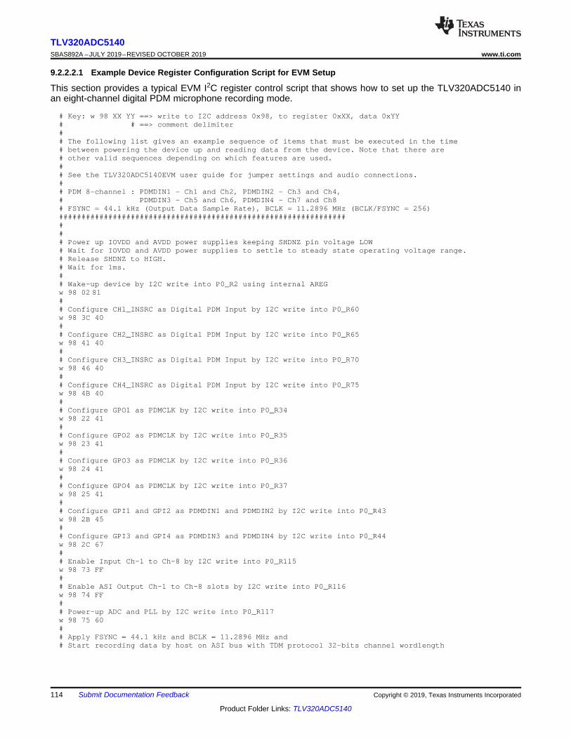
114
TLV320ADC5140SBAS892A –JULY 2019–REVISED OCTOBER 2019 www.ti.com
Product Folder Links: TLV320ADC5140
Submit Documentation Feedback Copyright © 2019, Texas Instruments Incorporated
9.2.2.2.1 Example Device Register Configuration Script for EVM Setup
This section provides a typical EVM I2C register control script that shows how to set up the TLV320ADC5140 inan eight-channel digital PDM microphone recording mode.
# Key: w 98 XX YY ==> write to I2C address 0x98, to register 0xXX, data 0xYY# # ==> comment delimiter## The following list gives an example sequence of items that must be executed in the time# between powering the device up and reading data from the device. Note that there are# other valid sequences depending on which features are used.## See the TLV320ADC5140EVM user guide for jumper settings and audio connections.## PDM 8-channel : PDMDIN1 - Ch1 and Ch2, PDMDIN2 - Ch3 and Ch4,# PDMDIN3 - Ch5 and Ch6, PDMDIN4 - Ch7 and Ch8# FSYNC = 44.1 kHz (Output Data Sample Rate), BCLK = 11.2896 MHz (BCLK/FSYNC = 256)################################################################### Power up IOVDD and AVDD power supplies keeping SHDNZ pin voltage LOW# Wait for IOVDD and AVDD power supplies to settle to steady state operating voltage range.# Release SHDNZ to HIGH.# Wait for 1ms.## Wake-up device by I2C write into P0_R2 using internal AREGw 98 02 81## Configure CH1_INSRC as Digital PDM Input by I2C write into P0_R60w 98 3C 40## Configure CH2_INSRC as Digital PDM Input by I2C write into P0_R65w 98 41 40## Configure CH3_INSRC as Digital PDM Input by I2C write into P0_R70w 98 46 40## Configure CH4_INSRC as Digital PDM Input by I2C write into P0_R75w 98 4B 40## Configure GPO1 as PDMCLK by I2C write into P0_R34w 98 22 41## Configure GPO2 as PDMCLK by I2C write into P0_R35w 98 23 41## Configure GPO3 as PDMCLK by I2C write into P0_R36w 98 24 41## Configure GPO4 as PDMCLK by I2C write into P0_R37w 98 25 41## Configure GPI1 and GPI2 as PDMDIN1 and PDMDIN2 by I2C write into P0_R43w 98 2B 45## Configure GPI3 and GPI4 as PDMDIN3 and PDMDIN4 by I2C write into P0_R44w 98 2C 67## Enable Input Ch-1 to Ch-8 by I2C write into P0_R115w 98 73 FF## Enable ASI Output Ch-1 to Ch-8 slots by I2C write into P0_R116w 98 74 FF## Power-up ADC and PLL by I2C write into P0_R117w 98 75 60## Apply FSYNC = 44.1 kHz and BCLK = 11.2896 MHz and# Start recording data by host on ASI bus with TDM protocol 32-bits channel wordlength
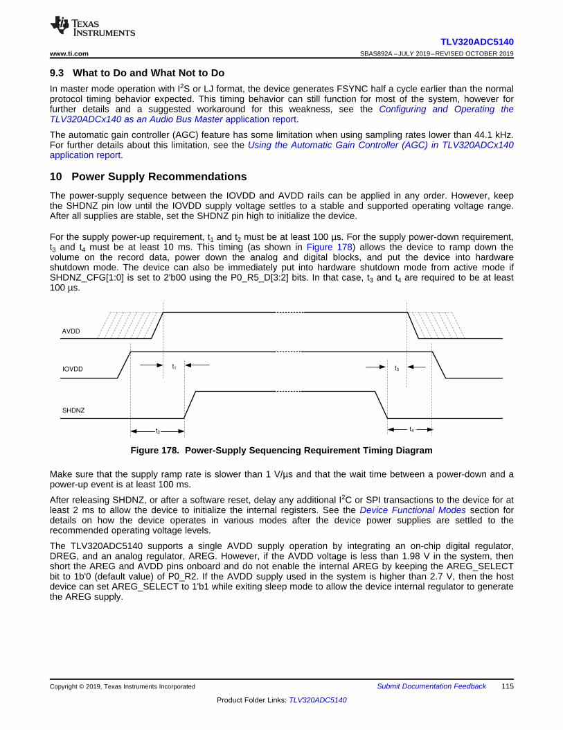
AVDD
IOVDD
SHDNZ
t1
t2
t3
t4
115
TLV320ADC5140www.ti.com SBAS892A –JULY 2019–REVISED OCTOBER 2019
Product Folder Links: TLV320ADC5140
Submit Documentation FeedbackCopyright © 2019, Texas Instruments Incorporated
9.3 What to Do and What Not to DoIn master mode operation with I2S or LJ format, the device generates FSYNC half a cycle earlier than the normalprotocol timing behavior expected. This timing behavior can still function for most of the system, however forfurther details and a suggested workaround for this weakness, see the Configuring and Operating theTLV320ADCx140 as an Audio Bus Master application report.
The automatic gain controller (AGC) feature has some limitation when using sampling rates lower than 44.1 kHz.For further details about this limitation, see the Using the Automatic Gain Controller (AGC) in TLV320ADCx140application report.
10 Power Supply RecommendationsThe power-supply sequence between the IOVDD and AVDD rails can be applied in any order. However, keepthe SHDNZ pin low until the IOVDD supply voltage settles to a stable and supported operating voltage range.After all supplies are stable, set the SHDNZ pin high to initialize the device.
For the supply power-up requirement, t1 and t2 must be at least 100 µs. For the supply power-down requirement,t3 and t4 must be at least 10 ms. This timing (as shown in Figure 178) allows the device to ramp down thevolume on the record data, power down the analog and digital blocks, and put the device into hardwareshutdown mode. The device can also be immediately put into hardware shutdown mode from active mode ifSHDNZ_CFG[1:0] is set to 2'b00 using the P0_R5_D[3:2] bits. In that case, t3 and t4 are required to be at least100 µs.
Figure 178. Power-Supply Sequencing Requirement Timing Diagram
Make sure that the supply ramp rate is slower than 1 V/µs and that the wait time between a power-down and apower-up event is at least 100 ms.
After releasing SHDNZ, or after a software reset, delay any additional I2C or SPI transactions to the device for atleast 2 ms to allow the device to initialize the internal registers. See the Device Functional Modes section fordetails on how the device operates in various modes after the device power supplies are settled to therecommended operating voltage levels.
The TLV320ADC5140 supports a single AVDD supply operation by integrating an on-chip digital regulator,DREG, and an analog regulator, AREG. However, if the AVDD voltage is less than 1.98 V in the system, thenshort the AREG and AVDD pins onboard and do not enable the internal AREG by keeping the AREG_SELECTbit to 1b'0 (default value) of P0_R2. If the AVDD supply used in the system is higher than 2.7 V, then the hostdevice can set AREG_SELECT to 1'b1 while exiting sleep mode to allow the device internal regulator to generatethe AREG supply.
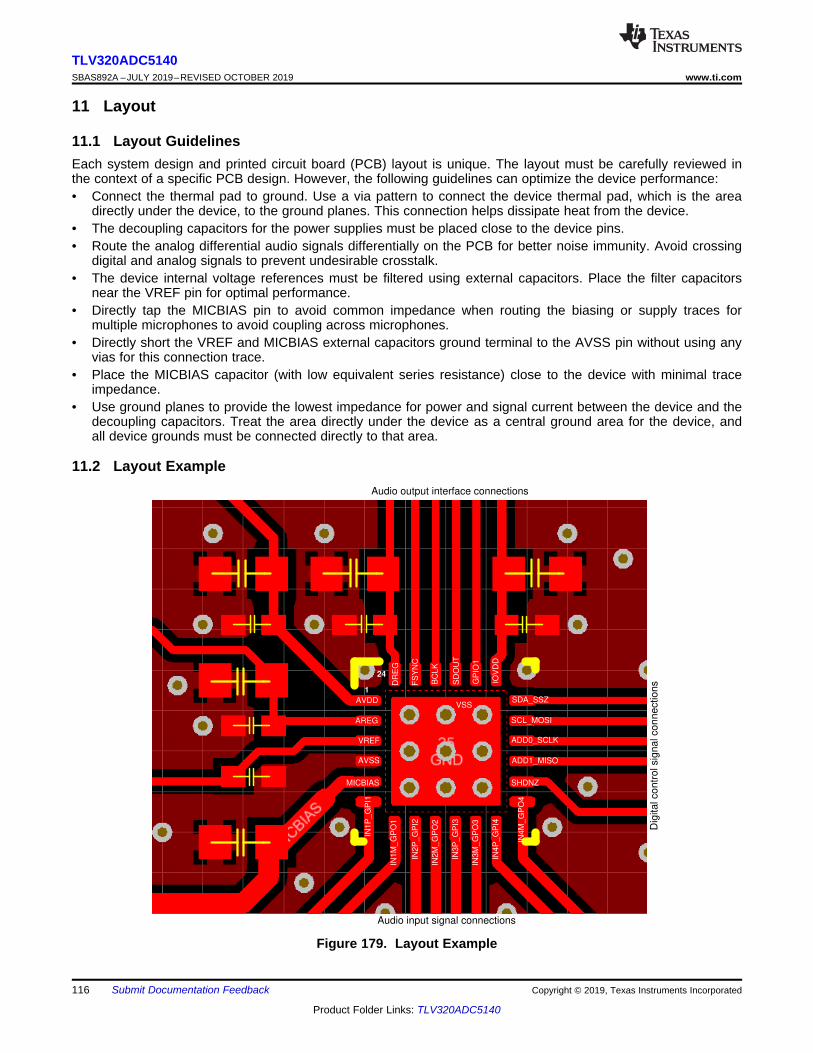
1
24
AVDD
AREG
VREF
AVSS
MICBIAS
IN1P
_G
PI1
IN1
M_
GP
O1
IN2
P_G
PI2
IN2
M_
GP
O2
IN3P
_G
PI3
IN3
M_
GP
O3
IN4
P_G
PI4
IN4M
_G
PO
4
SHDNZ
ADD1_MISO
ADD0_SCLK
SCL_MOSI
SDA_SSZ
IOV
DD
GP
IO1
SD
OU
T
BC
LK
FS
YN
C
DR
EG
Audio output interface connections
Dig
ita
l co
ntr
ol sig
na
l co
nn
ectio
ns
Audio input signal connections
VSS
116
TLV320ADC5140SBAS892A –JULY 2019–REVISED OCTOBER 2019 www.ti.com
Product Folder Links: TLV320ADC5140
Submit Documentation Feedback Copyright © 2019, Texas Instruments Incorporated
11 Layout
11.1 Layout GuidelinesEach system design and printed circuit board (PCB) layout is unique. The layout must be carefully reviewed inthe context of a specific PCB design. However, the following guidelines can optimize the device performance:• Connect the thermal pad to ground. Use a via pattern to connect the device thermal pad, which is the area
directly under the device, to the ground planes. This connection helps dissipate heat from the device.• The decoupling capacitors for the power supplies must be placed close to the device pins.• Route the analog differential audio signals differentially on the PCB for better noise immunity. Avoid crossing
digital and analog signals to prevent undesirable crosstalk.• The device internal voltage references must be filtered using external capacitors. Place the filter capacitors
near the VREF pin for optimal performance.• Directly tap the MICBIAS pin to avoid common impedance when routing the biasing or supply traces for
multiple microphones to avoid coupling across microphones.• Directly short the VREF and MICBIAS external capacitors ground terminal to the AVSS pin without using any
vias for this connection trace.• Place the MICBIAS capacitor (with low equivalent series resistance) close to the device with minimal trace
impedance.• Use ground planes to provide the lowest impedance for power and signal current between the device and the
decoupling capacitors. Treat the area directly under the device as a central ground area for the device, andall device grounds must be connected directly to that area.
11.2 Layout Example
Figure 179. Layout Example
117
TLV320ADC5140www.ti.com SBAS892A –JULY 2019–REVISED OCTOBER 2019
Product Folder Links: TLV320ADC5140
Submit Documentation FeedbackCopyright © 2019, Texas Instruments Incorporated
12 Device and Documentation Support
12.1 Documentation Support
12.1.1 Related DocumentationFor related documentation see the following:• Texas Instruments, Multiple TLV320ADCx140 Devices With a Shared TDM and I2C Bus application report• Texas Instruments, Configuring and Operating the TLV320ADCx140 as an Audio Bus Master application
report• Texas Instruments, TLV320ADCx140 Sampling Rates and Programmable Processing Blocks Supported
application report• Texas Instruments, TLV320ADCx140 Programmable Biquad Filter Configuration and Applications application
report• Texas Instruments, TLV320ADCx140 Operation for Low-Power Critical Applications application report• Texas Instruments, TLV320ADCx140 Power Consumption Matrix Across Various Usage Scenarios
application report• Texas Instruments, TLV320ADCx140 Integrated Analog Antialiasing Filter and Flexible Digital Filter
application report• Texas Instruments, Using the Automatic Gain Controller (AGC) in TLV320ADCx140 application report• Texas Instruments, Using the Dynamic Range Enhancer (DRE) in TLV320ADC5140/6140 application report• Texas Instruments, TLV320ADCx140 Evaluation module user's guide• Texas Instruments, PurePath™ Console Graphical Development Suite for Audio System Design and
Development
12.2 Receiving Notification of Documentation UpdatesTo receive notification of documentation updates, navigate to the device product folder on ti.com. In the upperright corner, click on Alert me to register and receive a weekly digest of any product information that haschanged. For change details, review the revision history included in any revised document.
12.3 Community ResourcesTI E2E™ support forums are an engineer's go-to source for fast, verified answers and design help — straightfrom the experts. Search existing answers or ask your own question to get the quick design help you need.
Linked content is provided "AS IS" by the respective contributors. They do not constitute TI specifications and donot necessarily reflect TI's views; see TI's Terms of Use.
12.4 TrademarksBurr-Brown, PurePath, E2E are trademarks of Texas Instruments.All other trademarks are the property of their respective owners.
12.5 Electrostatic Discharge CautionThis integrated circuit can be damaged by ESD. Texas Instruments recommends that all integrated circuits be handled withappropriate precautions. Failure to observe proper handling and installation procedures can cause damage.
ESD damage can range from subtle performance degradation to complete device failure. Precision integrated circuits may be moresusceptible to damage because very small parametric changes could cause the device not to meet its published specifications.
12.6 GlossarySLYZ022 — TI Glossary.
This glossary lists and explains terms, acronyms, and definitions.
118
TLV320ADC5140SBAS892A –JULY 2019–REVISED OCTOBER 2019 www.ti.com
Product Folder Links: TLV320ADC5140
Submit Documentation Feedback Copyright © 2019, Texas Instruments Incorporated
13 Mechanical, Packaging, and Orderable InformationThe following pages include mechanical, packaging, and orderable information. This information is the mostcurrent data available for the designated devices. This data is subject to change without notice and revision ofthis document. For browser-based versions of this data sheet, refer to the left-hand navigation.
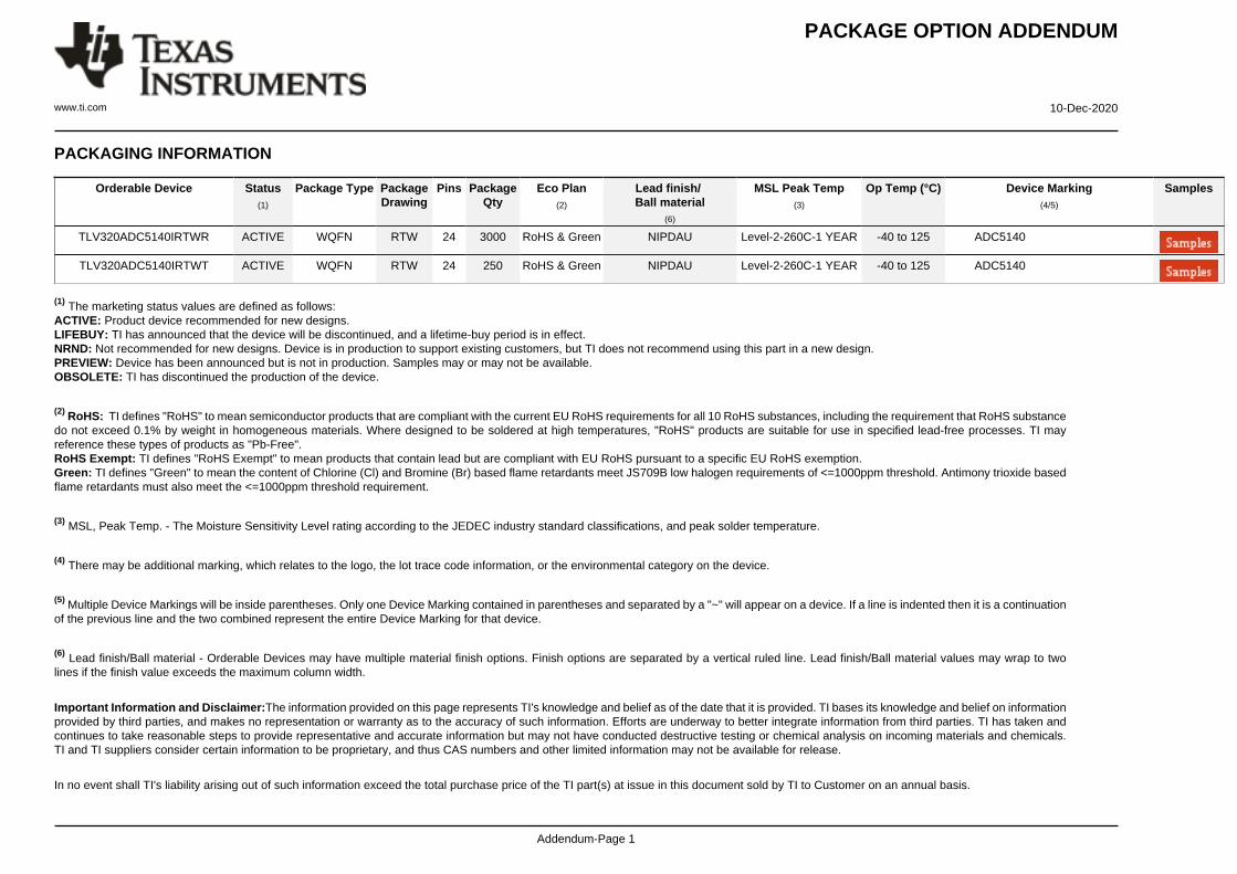
PACKAGE OPTION ADDENDUM
www.ti.com 10-Dec-2020
Addendum-Page 1
PACKAGING INFORMATION
Orderable Device Status(1)
Package Type PackageDrawing
Pins PackageQty
Eco Plan(2)
Lead finish/Ball material
(6)
MSL Peak Temp(3)
Op Temp (°C) Device Marking(4/5)
Samples
TLV320ADC5140IRTWR ACTIVE WQFN RTW 24 3000 RoHS & Green NIPDAU Level-2-260C-1 YEAR -40 to 125 ADC5140
TLV320ADC5140IRTWT ACTIVE WQFN RTW 24 250 RoHS & Green NIPDAU Level-2-260C-1 YEAR -40 to 125 ADC5140
(1) The marketing status values are defined as follows:ACTIVE: Product device recommended for new designs.LIFEBUY: TI has announced that the device will be discontinued, and a lifetime-buy period is in effect.NRND: Not recommended for new designs. Device is in production to support existing customers, but TI does not recommend using this part in a new design.PREVIEW: Device has been announced but is not in production. Samples may or may not be available.OBSOLETE: TI has discontinued the production of the device.
(2) RoHS: TI defines "RoHS" to mean semiconductor products that are compliant with the current EU RoHS requirements for all 10 RoHS substances, including the requirement that RoHS substancedo not exceed 0.1% by weight in homogeneous materials. Where designed to be soldered at high temperatures, "RoHS" products are suitable for use in specified lead-free processes. TI mayreference these types of products as "Pb-Free".RoHS Exempt: TI defines "RoHS Exempt" to mean products that contain lead but are compliant with EU RoHS pursuant to a specific EU RoHS exemption.Green: TI defines "Green" to mean the content of Chlorine (Cl) and Bromine (Br) based flame retardants meet JS709B low halogen requirements of <=1000ppm threshold. Antimony trioxide basedflame retardants must also meet the <=1000ppm threshold requirement.
(3) MSL, Peak Temp. - The Moisture Sensitivity Level rating according to the JEDEC industry standard classifications, and peak solder temperature.
(4) There may be additional marking, which relates to the logo, the lot trace code information, or the environmental category on the device.
(5) Multiple Device Markings will be inside parentheses. Only one Device Marking contained in parentheses and separated by a "~" will appear on a device. If a line is indented then it is a continuationof the previous line and the two combined represent the entire Device Marking for that device.
(6) Lead finish/Ball material - Orderable Devices may have multiple material finish options. Finish options are separated by a vertical ruled line. Lead finish/Ball material values may wrap to twolines if the finish value exceeds the maximum column width.
Important Information and Disclaimer:The information provided on this page represents TI's knowledge and belief as of the date that it is provided. TI bases its knowledge and belief on informationprovided by third parties, and makes no representation or warranty as to the accuracy of such information. Efforts are underway to better integrate information from third parties. TI has taken andcontinues to take reasonable steps to provide representative and accurate information but may not have conducted destructive testing or chemical analysis on incoming materials and chemicals.TI and TI suppliers consider certain information to be proprietary, and thus CAS numbers and other limited information may not be available for release.
In no event shall TI's liability arising out of such information exceed the total purchase price of the TI part(s) at issue in this document sold by TI to Customer on an annual basis.
PACKAGE OPTION ADDENDUM
www.ti.com 10-Dec-2020
Addendum-Page 2
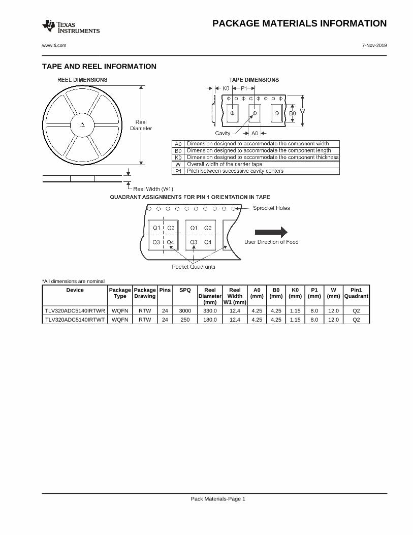
TAPE AND REEL INFORMATION
*All dimensions are nominal
Device PackageType
PackageDrawing
Pins SPQ ReelDiameter
(mm)
ReelWidth
W1 (mm)
A0(mm)
B0(mm)
K0(mm)
P1(mm)
W(mm)
Pin1Quadrant
TLV320ADC5140IRTWR WQFN RTW 24 3000 330.0 12.4 4.25 4.25 1.15 8.0 12.0 Q2
TLV320ADC5140IRTWT WQFN RTW 24 250 180.0 12.4 4.25 4.25 1.15 8.0 12.0 Q2
PACKAGE MATERIALS INFORMATION
www.ti.com 7-Nov-2019
Pack Materials-Page 1
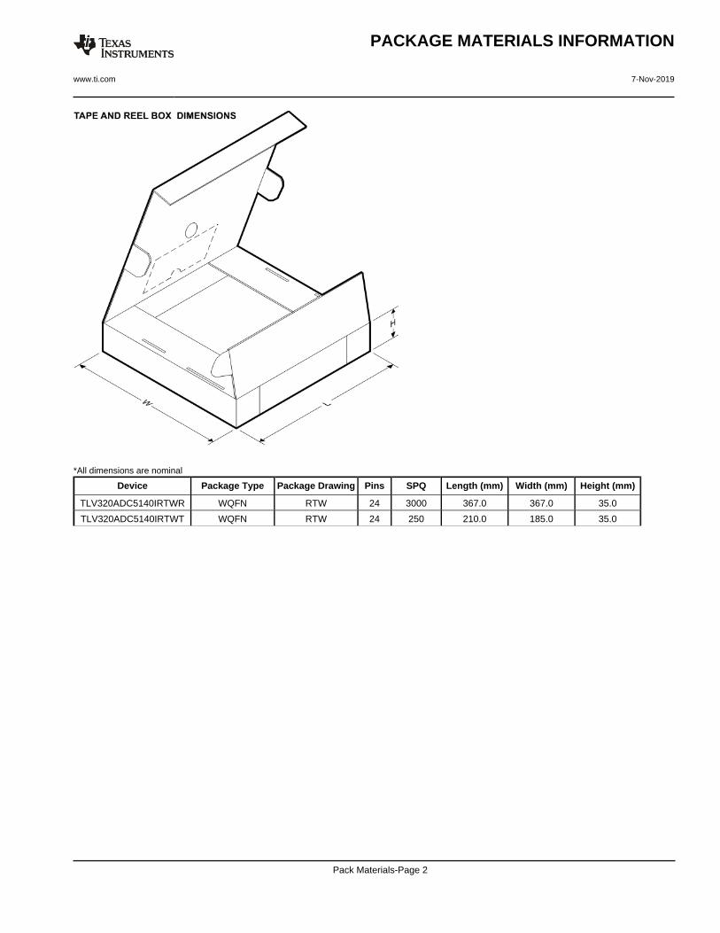
*All dimensions are nominal
Device Package Type Package Drawing Pins SPQ Length (mm) Width (mm) Height (mm)
TLV320ADC5140IRTWR WQFN RTW 24 3000 367.0 367.0 35.0
TLV320ADC5140IRTWT WQFN RTW 24 250 210.0 185.0 35.0
PACKAGE MATERIALS INFORMATION
www.ti.com 7-Nov-2019
Pack Materials-Page 2
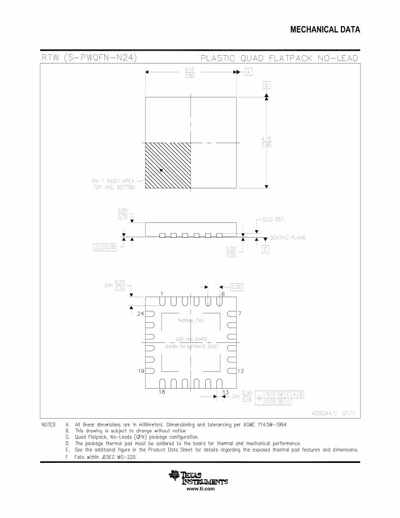

IMPORTANT NOTICE AND DISCLAIMER
TI PROVIDES TECHNICAL AND RELIABILITY DATA (INCLUDING DATASHEETS), DESIGN RESOURCES (INCLUDING REFERENCE DESIGNS), APPLICATION OR OTHER DESIGN ADVICE, WEB TOOLS, SAFETY INFORMATION, AND OTHER RESOURCES “AS IS” AND WITH ALL FAULTS, AND DISCLAIMS ALL WARRANTIES, EXPRESS AND IMPLIED, INCLUDING WITHOUT LIMITATION ANY IMPLIED WARRANTIES OF MERCHANTABILITY, FITNESS FOR A PARTICULAR PURPOSE OR NON-INFRINGEMENT OF THIRD PARTY INTELLECTUAL PROPERTY RIGHTS.These resources are intended for skilled developers designing with TI products. You are solely responsible for (1) selecting the appropriate TI products for your application, (2) designing, validating and testing your application, and (3) ensuring your application meets applicable standards, and any other safety, security, or other requirements. These resources are subject to change without notice. TI grants you permission to use these resources only for development of an application that uses the TI products described in the resource. Other reproduction and display of these resources is prohibited. No license is granted to any other TI intellectual property right or to any third party intellectual property right. TI disclaims responsibility for, and you will fully indemnify TI and its representatives against, any claims, damages, costs, losses, and liabilities arising out of your use of these resources.TI’s products are provided subject to TI’s Terms of Sale (www.ti.com/legal/termsofsale.html) or other applicable terms available either on ti.com or provided in conjunction with such TI products. TI’s provision of these resources does not expand or otherwise alter TI’s applicable warranties or warranty disclaimers for TI products.
Mailing Address: Texas Instruments, Post Office Box 655303, Dallas, Texas 75265Copyright © 2020, Texas Instruments Incorporated