Embed Size (px)
Citation preview

TlBr raw material purification, crystal growth, annealing, detector fabrication and characterisation for gamma-ray
detector applications
Vasilij Kozlov
Laboratory of Inorganic Chemistry
Department of Chemistry
Faculty of Science
University of Helsinki
Finland
Academic Dissertation
To be presented, with the permission of the Faculty of Science of the University of Helsinki, for public criticism in Auditorium A110 of the Department of Chemistry, A. I. Virtasen Aukio 1, on March 12th 2010 at 12 o’clock noon.
Helsinki, 2010
brought to you by COREView metadata, citation and similar papers at core.ac.uk
provided by Helsingin yliopiston digitaalinen arkisto

ii
Supervisor Prof. Markku Leskelä
Laboratory of Inorganic Chemistry
Department of Chemistry
University of Helsinki
Helsinki, Finland
Reviewers Prof. Stanislav Pospisil
Institute of Experimental and Applied Physics
Czech Technical University in Prague
Czech Republic
Dr. Keitaro Hitomi
Department of Electronics
Tohoku Institute of Technology
Japan
Opponent Prof. Juozas Vaitkus
Department of Semiconductor Physics,
Institute of Materials Science and Applied Research
Vilnius University
Lithuania
© Vasilij Kozlov 2010
ISBN 978-952-92-6915-0 (paperback)
ISBN 978-952-10-6104-2 (PDF version)
http://ethesis.helsinki.fi
Yliopistopaino
Helsinki 2010
iii
Abstract The research reported in this thesis dealt with single crystals of thallium bromide grown
for gamma-ray detector applications. The crystals were used to fabricate room temperature
gamma-ray detectors. Routinely produced TlBr detectors often are poor quality. Therefore,
this study concentrated on developing the manufacturing processes for TlBr detectors and
methods of characterisation that can be used for optimisation of TlBr purity and crystal
quality.
The processes under concern were TlBr raw material purification, crystal growth,
annealing and detector fabrication. The study focused on single crystals of TlBr grown from
material purified by a hydrothermal recrystallisation method. In addition, hydrothermal
conditions for synthesis, recrystallisation, crystal growth and annealing of TlBr crystals were
examined. The final manufacturing process presented in this thesis deals with TlBr material
purified by the Bridgman method. Then, material is hydrothermally recrystallised in pure
water. A travelling molten zone (TMZ) method is used for additional purification of the
recrystallised product and then for the final crystal growth. Subsequent processing is similar
to that described in the literature.
In this thesis, literature on improving quality of TlBr material/crystal and detector
performance is reviewed. Aging aspects as well as the influence of different factors
(temperature, time, electrode material and so on) on detector stability are considered and
examined. The results of the process development are summarised and discussed. This thesis
shows the considerable improvement in the charge carrier properties of a detector due to
additional purification by hydrothermal recrystallisation. As an example, a thick (4 mm) TlBr
detector produced by the process was fabricated and found to operate successfully in gamma-
ray detection, confirming the validity of the proposed purification and technological steps.
However, for the complete improvement of detector performance, further developments in
crystal growth are required.
The detector manufacturing process was optimized by characterisation of material and
crystals using methods such as X-ray diffraction (XRD), polarisation microscopy, high-
resolution inductively coupled plasma mass (HR-ICPM), Fourier transform infrared (FTIR),
ultraviolet and visual (UV-Vis) spectroscopy, field emission scanning electron microscope
(FESEM) and energy-dispersive X-ray spectroscopy (EDS), current-voltage (I-V) and
capacity voltage (CV) characterisation, and photoconductivity, as well direct detector
examination.
iv
Preface The experimental work presented in this thesis was done in the Laboratory of Inorganic
Chemistry at the University of Helsinki during the years 2000-2008. The work has been
funded by the European Space Agency (ESA) and Finnish Research Programme for Space
Research (ANTARES), and supported by the University of Helsinki, the Academy of Finland,
the Finnish National Technology Agency (TEKES) and the Finnish Inorganic Materials
Chemistry Graduate Program.
Firstly, I wish to thank my supervisor, Prof. Markku Leskelä, for the opportunity to work
with him in the field of materials science, and for providing the topic for this research. His
expert advice and guidance during the work gave new perspectives to my project. I am
grateful to my co-workers from Oxford Instruments Analytical Oy (Finland) for their support
and help in creating the TMZ installation and degassing system, and especially to Heikki
Sipilä, Seppo Nenonen and Hans Andersson for fruitful talks, meetings and collaboration.
Long term cooperation with Heikki Sipilä resulted in productive discussions with great impact
on the experimental work.
I would also like to sincerely thank the entire personnel of the Inorganic Chemistry
Laboratory for helpful discussions and technical assistance. Ilpo Mutikainen and Jarno
Kansikas are acknowledged for their quick guidance and technical solutions for many
problems. I’d like to express my gratitude to Marianna Kemell, Marko Vehkamäki and Mikko
Heikkilä for their patient help in imaging with SEM, deposition of metallic electrodes and
XRD 2��� scan measurements, respectively. I’d like to also express appreciation to Jaana
Valo for her interest in the topic and general discussions. I am especially grateful to
collaborators from the Institute of Chemistry (Vienna, Austria) and particularly to Thomas
Prohaska for performing the ICPMS measurements and trace element analysis. Vladimir
Gostilo and his colleagues (Bruker Baltic, Latvia) are thanked for their cooperation with
sample production and measurement of detector properties. I’d like to express gratitude to
Igorj Lisitsky and his co-workers (GIREDMET, Russia) for supplying TlBr raw material and
a series of samples, and to Pasi Kostamo (HUT, Finland) for fruitful collaboration.
Finally, I want to embrace my wonderful family, especially my wife Natalia, my children
Irina and Peter, and our mummi – they all encouraged and gave me additional strength to
perform this work. Also, many thanks to our dog Lordik, whose bright life and emotions
charged me during the whole process of this work.
Espoo/Helsinki, 17 August 2009 Vasilij Kozlov
v
List of Original Publications This thesis is based on 7 original publications, which are referred in the text by Roman
numerals.
I V. Kozlov, M. Leskelä, T. Prohaska, G. Schultheis, G. Stingeder, H. Sipilä, TlBr
crystal growth, purification and characterisation, Nucl. Instr. and Meth. A 531 (2004) 165 –
173.
II V. Kozlov, M. Leskelä and H. Sipilä, Annealing and characterisation of TlBr
crystals for detector applications, Nucl. Instr. and Meth. A 546 (2005) 200 – 204.
III V. Kozlov, M. Leskelä, M. Kemell, H. Sipilä, Effects of polishing and etching on
TlBr single crystals, Nucl. Instr. and Meth. A 563(1) (2006) 58 – 61.
IV V. Kozlov, M. Leskelä, M. Vehkamäki, H. Sipilä, Effects of metallisation of TlBr
single crystals for detector applications, Nucl. Instr. and Meth. A 573 (2007) 212 – 215.
V V. Kozlov, M. Kemell, M. Vehkamäki, M. Leskelä, Degradation effects in TlBr
single crystals under prolonged bias voltage, Nucl. Instr. and Meth. A 576 (2007) 10 – 14.
Va V. Kozlov, M. Kemell, M. Vehkamäki, M. Leskelä, Erratum to "Degradation
effects in TlBr single crystals under prolonged bias voltage" [Nucl. Instr. and Meth. A 576
(2007) 10–14], Nucl. Instr. and Meth. A 602 (2009) 625.
VI V. Kozlov, H. Andersson, V. Gostilo, M. Leskela, A. Owens, M. Shorohov, H.
Sipila, Improved process for the TlBr single-crystal detector, Nucl. Inst. and Meth. A 591/1
(2008) 209-212.
VII V. Kozlov, H. Andersson, V. Gostilo, M. Kemell, P. Kostamo, M. S. Kouznetsov,
M. Leskelä, H. Lipsanen, I. S. Lisitsky, M. Shorohov and H. Sipilä, Improvements and
problems of Bridgman–Stockbarger method for fabrication of TlBr single crystal detectors,
Nucl. Instr. and Meth. A 607 (2009) 126–128.
The original publications are printed with the permission of the Elsevier company.
vi
Related conference presentations by the same author V. Kozlov, M. Leskelä, T. Prohaska, G. Shultheis, G. Stingeder and H. Sipilä, TlBr crystal growth, purification
and characterisation, 5th International Workshop on Radiation Imaging Detectors, Riga, Latvia, 7-11 September 2003, Abstract Book, p. 50 (talk).
V. Kozlov, M. Leskelä, and H. Sipilä, Characterisation of TlBr crystals for detector applications, The 6th International Workshop on Radiation Imaging Detectors, Glasgow, Scotland, 25-29 July 2004, Abstracts, p.33 (talk).
V. Kozlov, M. Leskelä, M. Kemell, H. Sipilä, Effects of polishing and etching on TlBr single crystals, 7th International Workshop on Radiation Imaging Detectors, ESRF, Grenoble, France, 4-7 July 2005, Programme and Abstracts, p. 103 (poster).
V. Kozlov, M. Leskelä, M. Vehkamäki, H. Sipilä, Effects of metallization of TlBr single crystals for detector applications, 7th International Conference on Position Sensitive Detectors, University of Liverpool, 12-16 September 2005, Conference Programme, p. 21 (talk).
V. Kozlov, M. Leskelä, M. Kemell, M. Vehkamäki, Degradation effects in TlBr single crystals under prolonged bias voltage, 8th International Workshop on Radiation Imaging Detectors, Pisa, Italy, 2-6 July 2006, Programme and Abstracts, p. 37 (talk).
V. Kozlov, H. Andersson, M. Leskelä, H. Sipilä, Improved process for the detector grade TlBr single crystals, 2006 IEEE Room-Temperature Semiconductor Detector (RTSD) Workshop, October 30 - November 3, San Diego, CA, US, R06-27 (poster).
V. Kozlov, H. Andersson, V. Gostilo, M. Leskelä, M. Shorohov, H. Sipilä, A. Owens, Improved process for the TlBr single crystal detector, 9th International Workshop on Radiation Imaging Detectors, Erlangen, Germany, 22-26 July 2007, Abstracts, p. 42 (poster).
V. Kozlov, H. Andersson, V. Gostilo, P. Kostamo, M. S. Kouznetsov, M. Leskelä, H. Lipsanen, I. S. Lisitsky, M. Shorohov and H. Sipilä, Improved Bridgman-Stockbarger method for the TlBr single crystal detector, The 10th International Workshop on Radiation Imaging Detectors, June 29 - July 3, 2008, Helsinki, Finland, Abstract Book, p. 89 (poster).
Publications relevant to the current field of study N. Darovskikh, E. I. Zabidarov, V. I. Kozlov, G. A. Krutov, A. I. Kurbakov, A. A. Loshmanov, E. E. Rubinova,
V. A. Trunov, Investigations of monocrystalline structure perfections by means of a gamma-diffractometer, Preprint LINP, # 614, 1980. (rus)
V. I. Kozlov, A. A. Loshmanov, A. L. Malyshev, V. A. Trunov, V. A. Ulianov, The small-angle scattering of neutrons on the type A zeolite at its thermal destruction, Preprint LINP, # 862, 1983. (rus)
G. Gukasov, I. A. Zobkalo, V. I. Kozlov, V. P. Plakhty, Search for the effects of P-parity non-conservation in the crystals with the spiral magnetic structure, Preprint LINP, # 896, 1983. (rus)
V. I. Fedorov, A. G. Gukasov, V. Kozlov, S. V. Maleyev, V. P. Plakhty, I. A. Zobkalo, Interaction between the spin chirality and the elastic torsion, Physics Letters A 224 (1997) 372-378.
V. Kozlov, M. Leskelä, M. Kuznetsov, and I.S. Lisitsky, TlBr crystal characterisation using x-ray rocking curve method, 18th Nordic Structural Chemistry Meeting, Gustavelund Conference Center, Tuusula, Helsinki, Finland, 11-13 June 2004, Programme-Abstracts, p. P10 (poster).
P. Kostamo, M. Shorohov, V. Gostilo, H. Sipilä, V. Kozlov, I. Lisitsky, M. Kuznetsov, A. Lankinen, A.N. Danilewsky, H. Lipsanen, M. Leskelä, Characterization of TlBr for X-ray and �-ray detector applications, Nucl. Instr. and Meth. A 607/1 (2009) 129-131.

vii
List of Abbreviations
�G Free energy of Gibbs
μ Carrier mobility � Trapping time constant
Tl Vacancy in Tl site of lattice
ATR Attenuated total reflectance CERAC Trade mark of company
CHEMPUR Trade mark of company CSD Compound semiconductor detector
E Electric field E μ � Mean drift length before trapping
EB Electron beam EDS Energy-dispersive X-ray spectroscopy
Eg BandgapEPR Electron paramagnetic resonance
(FE)-SEM (Field emission) scanning electron microscope (FT)IR (Fourier transform) infrared spectroscopy
FWHM Full width at half maximum GIREDMET State Institute of rear earth metals (Russia)
HR-ICPMS High-resolution inductively coupled plasma mass spectrometry HSC HSC Chemistry 5.1 for Windows, software
I-V Voltage-current characteristics KRS-5 Mixture of TlBr and TlI: Br (46%) and I (54%)55
mp Melting point ND No data
PDF Powder diffraction file PTFE Polytetrafluorethylen
SIMS Secondary ion mass spectrometry TMZ Travelling molten zone
UV-Vis Ultraviolet and visual spectroscopy XRD X-ray diffraction methods

viii
Table of contents Abstract.............................................................................................................................iii
Preface .............................................................................................................................. iv List of Original Publications............................................................................................... v
Publications relevant to the current field of study .......................................................... vi List of Abbreviations........................................................................................................vii
Table of contents.............................................................................................................viii
1 Introduction.................................................................................................................... 1
2 Background.................................................................................................................... 3
2.1 Chemical properties ................................................................................................ 3 2.1.1 Electronic configuration and oxidation states of thallium ................................ 3 2.1.2 Tl(I) chemistry................................................................................................ 4 2.1.3 Tl(I) – Tl(III) mixed halides ............................................................................ 5 2.1.4 Tl(I) halides and impurities ............................................................................. 5
2.2 Physical properties.................................................................................................. 7 2.2.1 History............................................................................................................ 7 2.2.2 Criteria for the compound semiconductor as a gamma-ray detector ................. 9 2.2.3 Quality of industrial TlBr .............................................................................. 12
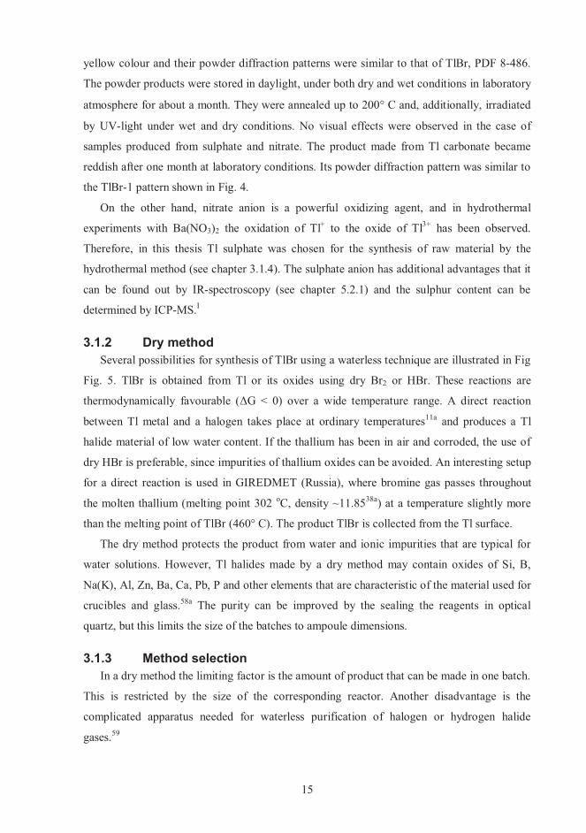
3 TlBr purification, crystal growth and annealing ............................................................ 13
3.1 TlBr raw material ................................................................................................. 13 3.1.1 Wet method .................................................................................................. 13
3.1.1.1 Aging effects......................................................................................... 14 3.1.1.2 Precursor effects.................................................................................... 14
3.1.2 Dry method................................................................................................... 15 3.1.3 Method selection........................................................................................... 15 3.1.4 Hydrothermal synthesis................................................................................. 16
3.2 Purification........................................................................................................... 17 3.2.1 Thermodynamics of separation and modelling .............................................. 18 3.2.2 Recrystallisation from vapour ....................................................................... 20 3.2.3 Recrystallisation from the molten state.......................................................... 21
3.2.3.1 Bridgman-Stockbarger method.............................................................. 21 3.2.3.2 Zone refinement .................................................................................... 22
3.2.4 Hydrothermal recrystallisation from solution ................................................ 24 3.2.5 Combination of purification methods ............................................................ 25
3.3 Crystal growth...................................................................................................... 26 3.3.1 Crystal perfection.......................................................................................... 26 3.3.2 Crystal growth from melt .............................................................................. 27
3.3.2.1 Crystal pulling....................................................................................... 27 3.3.2.2 Bridgman method.................................................................................. 27 3.3.2.3 Zone melting ......................................................................................... 29
3.3.3 Crystal growth from vapour .......................................................................... 30 3.3.4 Growth from solution.................................................................................... 31
3.3.4.1 Low-temperature methods..................................................................... 32
ix
3.3.4.2 Hydrothermal growth ............................................................................ 33
3.4 Annealing ............................................................................................................. 34 3.4.1 Types of annealing........................................................................................ 34 3.4.2 Processes associated with annealing.............................................................. 36
3.4.2.1 Strain-anneal method............................................................................. 36 3.4.2.2 Annealing of amorphous materials ........................................................ 37 3.4.2.3 Effects of impurities .............................................................................. 37
3.4.3 Annealing of single crystals of TlBr.............................................................. 38
4 TlBr detector fabrication .............................................................................................. 40
4.1 Slice preparation................................................................................................... 40
4.2 Chemical cutting and polishing............................................................................. 41 4.3 Etching ................................................................................................................. 42
4.4 Crystal orientation ................................................................................................ 44 4.5 Electrode deposition ............................................................................................. 46
4.5.1 Electrode choice and design .......................................................................... 46 4.5.2 Types of deposition....................................................................................... 47 4.5.3 Surface quality.............................................................................................. 48 4.5.4 Metal – Tl halide interactions........................................................................ 48 4.5.5 Metal – Tl halide interface stability............................................................... 50 4.5.6 Electro aging of the metal-TlBr interface ...................................................... 53
5 Characterisation methods ............................................................................................. 56
5.1 Microscope imaging techniques............................................................................ 57 5.1.1 Light polarisation microscopy....................................................................... 57 5.1.2 Field emission scanning electron microscopy (FE-SEM)............................... 58
5.2 Optical spectral methods....................................................................................... 60 5.2.1 FTIR spectra ................................................................................................. 61
5.3 X-ray diffraction methods (XRD) ......................................................................... 64 5.3.1 Penetration depth .......................................................................................... 65 5.3.2 Data collection and specimen displacement................................................... 66 5.3.3 Full width at half medium FWHM ................................................................ 66 5.3.4 Rocking curve method .................................................................................. 67
5.4 Electrical characterisation ..................................................................................... 69 5.5 Elemental analysis ................................................................................................ 69
Conclusion........................................................................................................................... 70
References ........................................................................................................................... 73

1
1 Introduction Among wide bandgap semiconductor materials single crystals of TlBr (2.68 eV) are the
most promising for use in room temperature gamma-ray detectors.1 The high stopping-power
of its elements [Zeff = (81+35)/2 = 58] and its density (7.56 g/cm3) make it unique and suitable
for space astrophysics, medicine and military applications. Unfortunately, TlBr is toxic and
soft, and both these properties considerably impede the development of TlBr as single
crystals. In addition, the use of TlBr crystals for gamma-ray detectors is still limited by the
quality of this material.2 Two characteristics of TlBr material, purity and crystal quality,
which are attributes of gamma-ray detectors,3 are still far from perfect.I, II
The aim of this thesis was to obtain the single crystals of high-purity and highest crystal
quality, which were suitable for X-ray and gamma-ray detection. When the experimental
work of this thesis was started, TlBr detectors were known to perform poorly, and their
mobility-lifetime products (μ�) were still impurity limited.4 Therefore, optical grade material,
which is purified by commonly used methods, crystallisation from vapour and melt, was
firstly applied for gamma-ray detectors. However, the produced detectors showed low
performance,I because material aimed for optics is not good enough for radiation detectors.51
The purity of TlBr could be improved in the zone refining process, since increasing the
number of refining passes from 20 to 50, increases resistivity and μ� by an order of
magnitude.5 On the other hand, the performance of TlBr material purified by 200-300 passes
has been limited by crystal imperfections that probably is originated during crystal growth
or/and detector fabrication.6 Thus, purity and crystal quality of TlBr are the most important
problems in the detector manufacturing process.
Two basic concepts were used in this thesis for solving these problems. For purification,
in addition to traditional methods used for obtaining optical grade materials, the
crystallisation from water solutions was applied. The basis of this is that TlBr samples
produced by melt methods and from water solutions were different with respect to impurity
composition, and removing soluble components was effective in pure water.I For crystal
quality improving, the annealing was used during the manufacturing process, because TlBr as
extremely soft material easily became damaged and contaminated.
Different methods were used for the preparation of high-purity TlBr material and single
crystals made from it. Since TlBr is sparingly soluble in water, the hydrothermal conditions
were applied. In general, the use of the hydrothermal method for synthesis, recrystallisation,
2
crystal growth and annealing is innovation for TlBr, the details of which are considered in
corresponding chapters.
This thesis consists of 7 publications and a summary text, in which the factors affecting
the purity of the TlBr material, crystal quality, and detector performance were studied. In
paper I, TlBr single crystals of different origins were studied by trace element analysis, and
hydrothermal methods were for the first time used for purification purpose. In paper II,
different types of annealing were used to improve the crystal quality of TlBr crystals; and
annealing effects on the electrical, optical and X-ray response properties were studied as well.
The effect on crystal quality of mechanical and chemical treatments, which are typically used
for detector fabrication, was studied in paper III. Different electrode materials and their roles
in TlBr-metal interfaces were described and examined in paper IV. Degradation of TlBr
devices and their electrical stability under prolonged bias voltage were studied in paper V.
The results of papers I-V were used in improvement of the total process for the TlBr
single-crystal detector, as it was reported77 and described in paper VI. The complete
improvement of detector performance was shown to require further developments in crystal
growth of TlBr. Several improvements in Bridgman-Stockbarger method and corresponding
failures in detector performance were discussed and analysed in paper VII.
The summary text of the thesis is organised as follows. In chapter 2 Background, the
properties of Tl halides and general information relevant to gamma-ray detectors are
considered and reviewed. TlBr purity and crystal quality are the most important
characteristics for room temperature gamma-ray detectors. Therefore, in this work special
attention has been paid to these qualities during TlBr purification, crystal growth and
annealing (chapter 3), as well, during detector fabrication (chapter 4). These characteristics
are also followed and treated in chapter 5, where instrumental methods used for optimisation
of the total manufacturing process are summarised. The summary text does not contain
separate chapters for literature review and experiments. These topics are included in the other
chapters. The results of the work and view to the future developments and applications of
TlBr single crystal detectors are presented in chapter Conclusion.

3
2 Background
2.1 Chemical properties Several specific features of the element thallium influence the chemical behaviour of TlBr
during the detector manufacturing process, and they are considered below.
2.1.1 Electronic configuration and oxidation states of thallium As expected from the electronic configuration (s2p1) of elements in Group 13, the great
majority of the compounds of Group 13 elements contain the element in oxidation state 3+.
However, the univalent state becomes progressively more stable as one descends down the
group7a and Tl(I) compounds are numerous.7c For thallium chemistry the Tl(I) – Tl(III)
relationship is a dominant feature.8 This phenomenon is associated with the so-called
Sidgwick inert electron pair effect.9 The term refers to the resistance of a pair of s electrons to
participation in covalent bond formation,8 and is much more pronounced for the heavier 6s2-
elements Hg, Tl, Pb and Bi, which form stable compounds with an oxidation state two units
less than would be expected. A more complete discussion of the inert electron pair effect is
given in Ref.10a For thallium, the 6s-shell stabilises Tl(I) compounds, which often resemble
the corresponding compounds of the alkali metals.7c
Although the oxidation state 3+ is less stable for thallium than for higher members of
Group 13, when all three electrons of thallium are used, the bonding is always covalent.7b
When the ionic character is pronounced for Tl(I) compounds, the impurity-admixture of
oxidation state 3+ should be considered as well. For example, when oxygen, nitrogen, or
sulphur bind to organic groups and also to Tl(I), the Tl-X bond appears to be more covalent
than the bond to alkali metal ions in similar compounds.8b
In solutions, complexation increases the probability of the Tl3+ state. As expected from the
high positive value of the redox potential (see Eq. 1), the Tl+ state is quite stable in aqueous
solutions. However, the potential decreases to +0.770 V in 1M HCl solution, due to the
presence of the complexing anion Cl-, which stabilises Tl3+ more than Tl+.8b
Tl3+ + 2e = Tl+, +1.26 V in 1M of HClO4 (Eq. 1)
The next trend influencing the Tl+/Tl3+ ratio in aqueous chemistry is the extensive
hydrolysis of Tl(III) ion to TlOH2+, from which it becomes the colloidal oxide even at pH
values from 1 to 2.5.8b In this work, the hydrolysis of Tl(I) was studied under hydrothermal
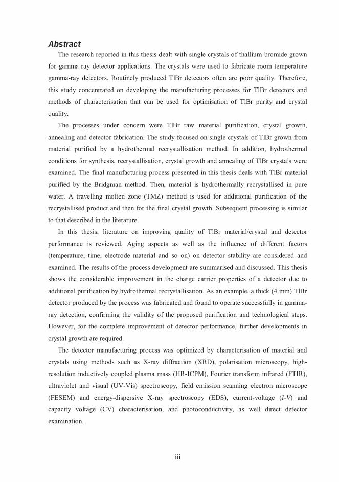
conditions. A black precipitate of Tl2O3 formed easily in alkali solutions (see Fig. 1). The
reaction was found to be favoured by increasing the temperature and/or pH. The minimum pH
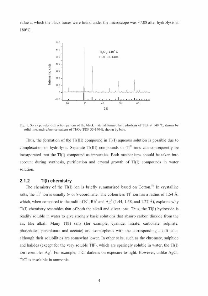
4
value at which the black traces were found under the microscope was ~7.08 after hydrolysis at
180�C.
20 30 40 50 60
-100
0
100
200
300
400
500
600
700
Tl2O3, 140o C
PDF 33-1404
Inte
nsity
, cnt
s
2�
Fig. 1. X-ray powder diffraction pattern of the black material formed by hydrolysis of TlBr at 140 oC, shown by solid line, and reference pattern of Tl2O3 (PDF 33-1404), shown by bars.
Thus, the formation of the Tl(III) compound in Tl(I) aqueous solution is possible due to
complexation or hydrolysis. Separate Tl(III) compounds or Tl3+-ions can consequently be
incorporated into the Tl(I) compound as impurities. Both mechanisms should be taken into
account during synthesis, purification and crystal growth of Tl(I) compounds in water
solution.
2.1.2 Tl(I) chemistry The chemistry of the Tl(I) ion is briefly summarized based on Cotton.8b In crystalline
salts, the Tl+ ion is usually 6- or 8-coordinate. The colourless Tl+ ion has a radius of 1.54 Å,
which, when compared to the radii of K+, Rb+ and Ag+ (1.44, 1.58, and 1.27 Å), explains why
Tl(I) chemistry resembles that of both the alkali and silver ions. Thus, the Tl(I) hydroxide is
readily soluble in water to give strongly basic solutions that absorb carbon dioxide from the
air, like alkali. Many Tl(I) salts (for example, cyanide, nitrate, carbonate, sulphate,
phosphates, perchlorate and acetate) are isomorphous with the corresponding alkali salts,
although their solubilities are somewhat lower. In other salts, such as the chromate, sulphide
and halides (except for the very soluble TlF), which are sparingly soluble in water, the Tl(I)
ion resembles Ag+. For example, TlCl darkens on exposure to light. However, unlike AgCl,
TlCl is insoluble in ammonia.

5
The photosensitivity of Tl is used in scintillation radiation detectors, which are made from
alkali halide crystals. Incorporation of Tl(I) halides into alkali halides gives rise to new
absorption and emission bands, thus, salts activated with thallium become phosphors. The
NMR signals of Tl(I) and Tl(III) are readily detected both in solutions and in solids. The
resonances are very sensitive to the environment and have large solvent-dependent shifts. For
Tl+ it is possible to correlate shifts with solvating ability.
2.1.3 Tl(I) – Tl(III) mixed halides Thallium (I) halides are quite stable. Tl(III) compounds are reduced to Tl(I) compounds in
solution and decompose with heating. However, thallium readily gives rise to intermediate
compounds which contain both Tl(I) and Tl(III).11a The action of bromine and chlorine on the
Tl(I) halide yields the Tl(III) compound, but well-defined intermediate compounds may be
isolated, as shown in Eq. 2:
Tl(I) [Tl(III)A4] = 2 TlA2 and Tl(I)3 [Tl(III)A6] = 2 Tl2A3, (Eq. 2)
where A is Cl or Br.7d Bromine gives these type of compounds more easily than chlorine. The
tri-iodide compound, however, is Tl(I)I�I2, but in water solution there is an equilibrium
between two isomeric forms of the tri-iodide: Tl(I) [I�I2] <=> Tl(III) [I]3.11b Therefore, the
formation of intermediate compounds can occur in Tl(I) halides if oxidant impurities are
present or can be formed during synthesis, purification or crystal growth from the vapour or
molten state.
2.1.4 Tl(I) halides and impurities One of the most important impurities in Tl halides is thallium itself which has been
oxidized during processing by the mechanisms described above. The oxidation can occur due
to environmental conditions, tools and materials used, or oxidant impurities present during
processing. The oxidised impurity can be in the form of a Tl(III) substance or Tl(I)-Tl(III)
intermediate compound, or the Tl3+-ion can be directly incorporated in a host lattice. If a
Tl(III) compound decomposes, the corresponding compound of Tl(I) contaminates the
thallium halide, as in case of Tl2O3, which is reduced to Tl2O during thermo-treatment.
A second source of impurities is the substitution of ions in the host lattice. Ions, which are
in the same oxidation state and with a radius similar to that of the ion they are replacing,
substitute easily for each other, since they produce less distortion of the lattice. Thus, the Tl+-
ion, which has radii of 1.50 Å in NaCl-type or 1.59 Å in CsCl-type lattices34b, can be replaced
by alkali, silver (see 2.1.2) and ammonium ions. Tl+ is a rather large ion and many other
cations can occupy its place. Substitution with ions in other oxidation states also inserts
6
vacancies because electro-neutrality must be maintained. For example, one Cd2+Tl Tl Br-
2
substitutes for two TlBr. Halide anions can substitute for each other, which is a serious purity
problem for Tl halides. Since Cl-, Br- and I- anions are large ions with the radii of 1.81 Å, 1.96
Å and 2.2 Å,34b respectively, many other anions and molecular groups can be incorporated
into the halide lattice.12 Impurity phenomena and theoretical explanations based on molecular
vibrations in crystals have been considered by Decius and Hexter.13a
The next source of impurities is the processing of a Tl halide in water solutions, where
insoluble compounds contaminate it. The elements of insoluble halides are located near one
another in the periodic table and act similarly chemically, particularly if their oxidation states
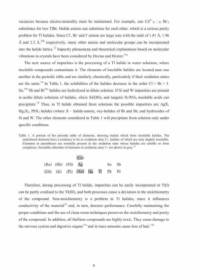
are the same.14 In Table 1, the solubilities of the halides decrease in the order Cl > Br > I.
Sn,15b Sb and Bi15c halides are hydrolysed in dilute solution. If Si and W impurities are present
in acidic dilute solutions of halides, silicic Si(OH)4 and tungstic H2WO4 insoluble acids can
precipitate.14 Thus, in Tl halide obtained from solutions the possible impurities are AgX,
Hg2X2, PbX2 halides (where X – halide-anion), oxy-halides of Bi and Sb, and hydroxides of
Si and W. The other elements considered in Table 1 will precipitate from solution only under
specific conditions.
Table 1. A portion of the periodic table of elements, showing metals which form insoluble halides. The underlined elements have a tendency to be in oxidation state 2+, halides of which are only slightly insoluble. Elements in parentheses are normally present in the oxidation state whose halides are soluble or form complexes. Insoluble chlorides of elements in oxidation state 1+ are shown in grey.14
(Cu)
(Ru) (Rh) (Pd) Ag Sn Sb
(Os) (Ir) (Pt) (Au) Hg Tl Pb Bi
Therefore, during processing of Tl halide, impurities can be easily incorporated or Tl(I)
can be partly oxidised to the Tl(III), and both processes cause a deviation in the stoichiometry
of the compound. Non-stoichiometry is a problem in Tl halides, since it influences
conductivity of the material16 and, in turn, detector performance. Carefully maintaining the
proper conditions and the use of clean room techniques preserves the stoichiometry and purity
of the compound. In addition, all thallium compounds are highly toxic. They cause damage to
the nervous system and digestive organs11a and in trace amounts cause loss of hair.15a
7
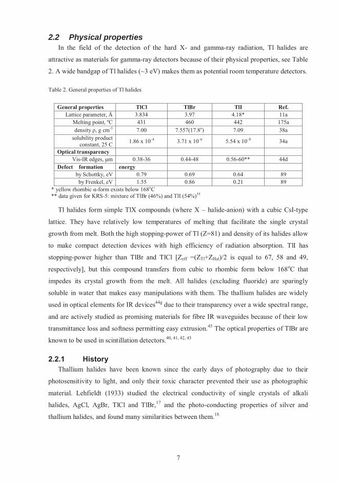
2.2 Physical properties In the field of the detection of the hard X- and gamma-ray radiation, Tl halides are
attractive as materials for gamma-ray detectors because of their physical properties, see Table
2. A wide bandgap of Tl halides (~3 eV) makes them as potential room temperature detectors.
Table 2. General properties of Tl halides
General properties TlCl TlBr TlI Ref. Lattice parameter, Å 3.834 3.97 4.18* 11a
Melting point, ºC 431 460 442 175adensity �, g cm-3 7.00 7.557(17.8o) 7.09 38a
solubility product constant, 25 C 1.86 x 10⁻⁴ 3.71 x 10⁻⁶ 5.54 x 10⁻⁸ 34a
Optical transparency Vis-IR edges, m 0.38-36 0.44-48 0.56-60** 44d
Defect formation energyby Schottky, eV 0.79 0.69 0.64 89by Frenkel, eV 1.55 0.86 0.21 89
* yellow rhombic -form exists below 168oC** data given for KRS-5: mixture of TlBr (46%) and TlI (54%)55
Tl halides form simple TlX compounds (where X – halide-anion) with a cubic CsI-type
lattice. They have relatively low temperatures of melting that facilitate the single crystal
growth from melt. Both the high stopping-power of Tl (Z=81) and density of its halides allow
to make compact detection devices with high efficiency of radiation absorption. TlI has
stopping-power higher than TlBr and TlCl [Zeff =(ZTl+ZHal)/2 is equal to 67, 58 and 49,
respectively], but this compound transfers from cubic to rhombic form below 168oC that
impedes its crystal growth from the melt. All halides (excluding fluoride) are sparingly
soluble in water that makes easy manipulations with them. The thallium halides are widely
used in optical elements for IR devices44g due to their transparency over a wide spectral range,
and are actively studied as promising materials for fibre IR waveguides because of their low
transmittance loss and softness permitting easy extrusion.45 The optical properties of TlBr are
known to be used in scintillation detectors.40, 41, 42, 43
2.2.1 History Thallium halides have been known since the early days of photography due to their
photosensitivity to light, and only their toxic character prevented their use as photographic
material. Lehfieldt (1933) studied the electrical conductivity of single crystals of alkali
halides, AgCl, AgBr, TlCl and TlBr,17 and the photo-conducting properties of silver and
thallium halides, and found many similarities between them.18

8
A halide crystal counter was first described in Van Heerden’s dissertation19 (1945), which
showed that silver chloride crystals at low temperature may detect gamma rays and - / �-
particles. Hofstadter1 (1947), knowing about Lehfieldt’s work, then extended Van Heerden’s
work to the Tl(I) halides. He found that, if mixed crystal TlBr0.4I0.6 (~KRS-5) was properly
prepared and annealed, it was able to detect gamma-radiation of Ra. He suggested the same
result for pure thallium bromide and thallium iodide. In 1949 Hofstadter published his work
on crystal counters using theoretical approaches20 to experiments with halide crystals.3 At that
time, halide compounds were thought to be the most promising materials for gamma-ray
detection, and nobody understood that the elemental semiconductors (Si and Ge) were
available for this purpose.
During the same time, in the field of semiconductor physics, Bardeen and Brattain (1948)
discovered the Ge transistor21 and described the nature of its contacts,22 and Shockley and
Pearson23 considered theoretically and studied experimentally conductance modulation by
surface charges. In 1949 McKay24 used Bardeen and Brattain’s results for making a barrier
layer in germanium and very successfully measured -ray pulses of Po. During the further
rapid development of the Ge and Si semiconductor industry, in fact, they were anticipated to
be primary radiation detectors.2 The compound semiconductors, such as the alkali-metal
halides, CdTe, CdZnTe and HgI2, received very little attention until the 1960s.25
At that time the optics industry was developing Tl halide materials for IR and night vision
devices. Therefore, optical transmittance and clarity were the main parameters for
optimization, for which other characteristics, such as purity and crystal quality, were
sacrificed. After the 1960s, progress in fabrication of compound semiconductor detectors
(CSDs) has been incremental.26 Nowadays, with regular missions into space, studies of the
universe generated the problem of cosmic ray detection without the use of special cryogenic
systems. As a result, attention once again turned to wide bandgap CSDs. CdTe, CdZnTe and
HgI2 radiation detectors were made commercially available; however, the individual devices
were mostly restricted to small sizes.26 Such quality factors as micro-crystallinity, high defect
densities, purity and stoichiometric imbalances considerably limited the carrier transport
properties of compound semiconductors.2
For future planetary and astrophysics missions, the development of high-resolution
imaging X-ray spectrometers is needed. Silicon-based imaging detectors are already well
developed, but their efficiency is limited in practice to 20 keV.27 Therefore, the search for and
improvement of CSD materials for the energy range 30-500 keV and higher, and for

9
specialized applications in which Ge, Si or scintillation detectors are unsuitable, is a current
task for CSD development.
2.2.2 Criteria for the compound semiconductor as a gamma-ray detector Since Hofstadter’s work,3 many researchers have formulated the requirements for
materials to be used as gamma and X-ray detectors. The material characteristics28 are
restricted by the type of radiation, detector construction, and limitations of measuring
techniques. The detection of various types of radiation by CSDs has been carefully considered
in the classical works of Dearnaley29 and Bertolini.30 There are several reviews25, 31, 32 of
materials for radiation detectors at elevated temperatures, from which some general criteria
for CSDs are summarised in Table 3.
Prince and Polishuk emphasised that a CSD should be a large uniform single crystal
without polarisation effects, and that the mobility-trap time product μ� should be stable over
operating temperatures. Among other features, they mentioned that a detector has to be low
cost, reproducible, reliable, and resistant to environmental conditions, with the 1st stage of a
preamplifier being included with the detector’s package.25 The CSD must be capable of
operating in the energy range 50 – 100 keV and have about 2% FWHM resolution.31
Table 3. Material and device requirements for gamma-ray CSDs to be used at elevated temperatures.
Evaluation parameter (1967)25 (1968),30 (1975)32
Depletion depths > 1mm Active area > 1 cm2
Thickness … ~2 mm Material high Z Z~40Bandgap Eg, eV > 1.3 ~1Min carrier mobility μ, cm2/(V s) 100 100μ �, cm2/V 10-5
Ionised dopant density, cm-3 < 1012 � 5x10¹¹
Trapping centre density … � 5x1012 cm-3
Temperature range, oC -50 to 300 Contacts non-injecting non-injecting Noise Noise free Leakage current < 10-5 A
In a simplified model of CSD in Fig. 2, a planar detector is operated by applying a voltage
across contacts on opposite sides of the device. Ionising radiation (gamma rays or charged
particles) produces at the absorption point a compact plasma cloud of the excited electron-
hole pairs in proportion to the energy of the radiation deposited in the detector. For a period of
time known as the plasma time, the plasma is inactive under the applied voltage, since any
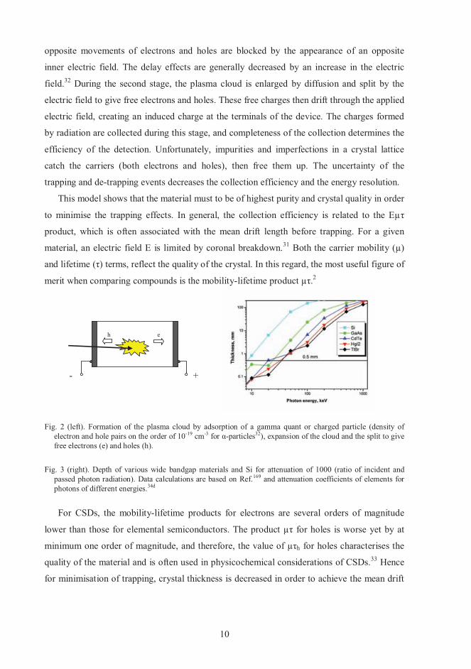
10
opposite movements of electrons and holes are blocked by the appearance of an opposite
inner electric field. The delay effects are generally decreased by an increase in the electric
field.32 During the second stage, the plasma cloud is enlarged by diffusion and split by the
electric field to give free electrons and holes. These free charges then drift through the applied
electric field, creating an induced charge at the terminals of the device. The charges formed
by radiation are collected during this stage, and completeness of the collection determines the
efficiency of the detection. Unfortunately, impurities and imperfections in a crystal lattice
catch the carriers (both electrons and holes), then free them up. The uncertainty of the
trapping and de-trapping events decreases the collection efficiency and the energy resolution.
This model shows that the material must to be of highest purity and crystal quality in order
to minimise the trapping effects. In general, the collection efficiency is related to the Eμ�
product, which is often associated with the mean drift length before trapping. For a given
material, an electric field E is limited by coronal breakdown.31 Both the carrier mobility (μ)
and lifetime (�) terms, reflect the quality of the crystal. In this regard, the most useful figure of
merit when comparing compounds is the mobility-lifetime product μ�.2
Fig. 2 (left). Formation of the plasma cloud by adsorption of a gamma quant or charged particle (density of electron and hole pairs on the order of 10-19 cm-3 for -particles32), expansion of the cloud and the split to give free electrons (e) and holes (h).
Fig. 3 (right). Depth of various wide bandgap materials and Si for attenuation of 1000 (ratio of incident and passed photon radiation). Data calculations are based on Ref.169 and attenuation coefficients of elements for photons of different energies.34d
For CSDs, the mobility-lifetime products for electrons are several orders of magnitude
lower than those for elemental semiconductors. The product μ� for holes is worse yet by at
minimum one order of magnitude, and therefore, the value of μ�h for holes characterises the
quality of the material and is often used in physicochemical considerations of CSDs.33 Hence
for minimisation of trapping, crystal thickness is decreased in order to achieve the mean drift
+-
eh

11
length of holes. For example, a thin crystal and a high electric field were used in the first Ge
detector.24
Thus, the quality of the material limits the maximum detector thickness, which is
determined by the mean drift length of holes. For many wide bandgap materials, a thickness
of 0.5 mm is mostly technically attainable. On the other hand, the attenuation of radiation
depends on material thickness (h) as exp(-μ�h), where μ is the mass attenuation coefficient
and � is material density. The attenuation efficiency of wide bandgap materials has been
evaluated by several authors.6, 35, 36 Plotted for a thickness of 0.5 mm it increases from Si to
GaAs, CdTe, HgI2 and TlBr.176 The depths of these high-Z materials presented in Fig. 3 as a
function of a photon energy at fixed 1000-fold attenuation show that the 0.5-mm thickness
limit should be considerably increased for hard X- and gamma-rays. Thus, improved quality
of materials is needed in order to make detectors of high energy photons.
The next problem is connected to the energy bandgap Eg: CSDs with a larger bandgap
have lower dark current and higher spectroscopic resolution,37 but they tend to have relatively
small carrier mobilities due to greater polar lattice carrier scattering.31 For room-temperature
radiation CSDs, the lower limit for Eg is set to ~1.4 eV, since in materials with a smaller
bandgap the carriers are thermally generated at room temperature. The highest bandgap is set
to ~3.5 eV, since for larger bandgap materials an increase in energy is required for the
electron-hole formation. Larger Eg values may also allow large values for the electrical
resistivity (R), allowing the application of larger electrical fields (E). However, in CSDs the
value of R itself depends additionally on stoichiometry, purity and the possible mixed
oxidation state of the metal in the compound, for example in halides of Tl+ and Tl3+, Pb2+ and
Pb4+, and Hg+ and Hg2+. 33
In a recent review on compound semiconductor radiation detectors, various wide bandgap
materials and the influence of their characteristics on detection and detector performance are
summarised and analysed.2 The wide bandgap is important for space astrophysics because it
allows device operation at near room temperature using a Peltier cooler. Among wide
bandgap semiconductor materials, single crystal TlBr (2.68 eV ) was chosen for the current
work. The high stopping power and density38a of TlBr make this material the leader among
other materials in completeness of gamma-ray absorption, as it is shown in Fig. 3. Both these
properties could be utilised in the kinds of compact and mobile devices that are needed for
express analysis and military applications. Moreover, the completeness of absorption could
decrease the dose deposited in a patient during X-/ gamma-ray medical courses. The recent
achievement of an inter-pixel resistance of ~500 G� with a gap of 100μm between the

12
electrodes at 50V in a small-format TlBr array39 makes TlBr an attractive material for
manufacturing a compact 2D-array detector in the field of hard X-ray imaging spectroscopy.
The high transparency of TlBr over a wide spectral range is utilised as well in this field, and
several scintillation and photo detectors using TlBr have been successfully manufactured.40, 41,
42, 43 Therefore, TlBr is a promising material for X-ray and gamma-ray room temperature
detectors, with many potential applications.
2.2.3 Quality of industrial TlBr As noted previously, the quality of Tl halides was improved for decades to enhance optical
transmittance. Tl halides transmit light over a wide range of visible and IR spectra (Table 2).
The short wavelength boundary has been found to be dependent on bandgap (Eg) of the
material, and long wavelength transmittance is limited by vibrations of the crystal lattice.44b
Attenuation and scattering losses have been studied in optical fibre materials45, 46, 47 since
these losses are, for example in KRS-5, three orders of magnitude above the intrinsic bulk
absorption at 10 m.47 The losses have been associated with impurity absorption45 and as well
with residual strain resulting from the manufacturing process.46 The most rational
parametrisation and numerical estimations of this problem have been done by Lines.48, 49
Experimental absorption coefficients in the long wavelength region are some what higher
than expected based on theory. When an impurity is built into the host lattice, scattering of
phonons increases, as a result, the attenuation of light enlarges with increasing impurity
content. When the concentration approaches the limit for a given impurity, its further increase
causes the formation of inclusions as a separate phase. At this stage, since local tension occurs
around the inclusions, the built-in impurities are forced out from lattice positions into the area
with higher tension. The lattice becomes more perfect and its absorption coefficient decreases,
but now Rayleigh scattering takes place on the inclusions.44c Further increasing the impurity
concentration produces visual effects and even degradation of the material.50 More details
about impurity effects and annealing are given in chapter 3.4.
Since the equilibrium between the amount of the impurity in the lattice and the formation
of inclusions depends on temperature, thermal treatments of the host material are optimised
for given impurities in order to maximise the optical transmittance.44c Instead of developing
methods of material purification, this method is used in the industry for improving clarity of
Tl halide optics. For example, several TlBr crystals used in our studies were grown with a
temperature drop of about 100 degrees between liquid and solid phases.51 These crystals

13
preserved the excess of impurities frozen in the lattice in a meta-stable state. More details
about these crystals are given in chapter 3.3.2.2.
In general, TlBr crystals produced for optics do not fit to requirements of gamma-ray
detectors because of impurities frozen in the lattice and strains caused by high temperature
gradients during the solidification. TlBr purity and crystal quality are the most important
characteristics for room temperature gamma-ray detectors, see chapter 2.2.2, above. In this
work special attention was paid to these qualities and they were studied during TlBr
purification, crystal growth and annealing as well during hydrothermal and aging treatments,
as described in next chapter 3.
3 TlBr purification, crystal growth and annealing
3.1 TlBr raw material Thallium halides are sparingly soluble in water (see Table 2), so the easiest way to obtain
halides is a precipitation reaction between the cation Tl+ and a corresponding anion A-: Tl+ +
A- => TlA �.7a With water solutions the method is quite flexible and widely used in industry.
Soluble sulphate and nitrate of thallium are conventionally combined with a salt or acid of the
corresponding halide. However, the routine operations removing by-product ions of the
mother solution, such as a decantation or a filtration, are not sufficient for the production of
optical grade material, because during the precipitation, thallium halides easily capture
impurities of Ag, Pb, Cu and Cd.52a Water itself as an impurity influences the properties of Tl
halides,53 therefore, synthesis methods are often classified as “wet” or “dry” based on the
presence or absence of water.
3.1.1 Wet methodIn order to improve optical properties of Tl halides, it has been recommended that reagents
of maximum purity be used for synthesis, for example, electrochemical grade Tl and its
nitrate as precursors for the precipitation reaction.52a In the case of a reaction with acid, excess
acid should be neutralised, for example, by alkali solution, but this increases the possibility of
hydrolysis of Tl+ to Tl3+ in subsequent operations, as described in chapter 2.1.1. The stability
of TlBr detectors is a current problem, therefore the aging and precursor effects on stability of
TlBr raw material were studied in this work.
14
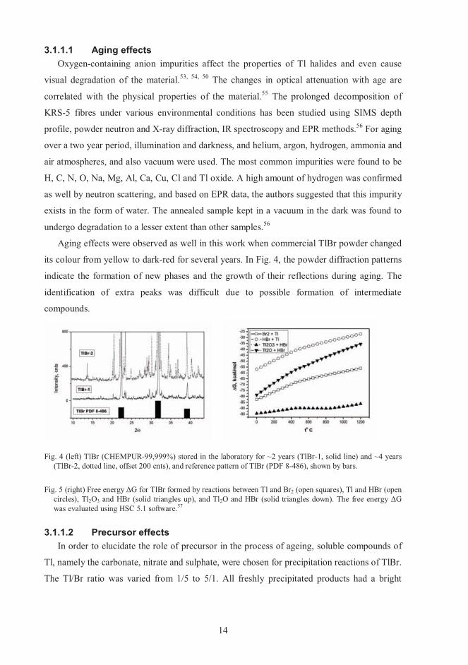
3.1.1.1 Aging effects Oxygen-containing anion impurities affect the properties of Tl halides and even cause
visual degradation of the material.53, 54, 50 The changes in optical attenuation with age are
correlated with the physical properties of the material.55 The prolonged decomposition of
KRS-5 fibres under various environmental conditions has been studied using SIMS depth
profile, powder neutron and X-ray diffraction, IR spectroscopy and EPR methods.56 For aging
over a two year period, illumination and darkness, and helium, argon, hydrogen, ammonia and
air atmospheres, and also vacuum were used. The most common impurities were found to be
H, C, N, O, Na, Mg, Al, Ca, Cu, Cl and Tl oxide. A high amount of hydrogen was confirmed
as well by neutron scattering, and based on EPR data, the authors suggested that this impurity
exists in the form of water. The annealed sample kept in a vacuum in the dark was found to
undergo degradation to a lesser extent than other samples.56
Aging effects were observed as well in this work when commercial TlBr powder changed
its colour from yellow to dark-red for several years. In Fig. 4, the powder diffraction patterns
indicate the formation of new phases and the growth of their reflections during aging. The
identification of extra peaks was difficult due to possible formation of intermediate
compounds.
Fig. 4 (left) TlBr (CHEMPUR-99,999%) stored in the laboratory for ~2 years (TlBr-1, solid line) and ~4 years (TlBr-2, dotted line, offset 200 cnts), and reference pattern of TlBr (PDF 8-486), shown by bars.
Fig. 5 (right) Free energy �G for TlBr formed by reactions between Tl and Br2 (open squares), Tl and HBr (open circles), Tl2O3 and HBr (solid triangles up), and Tl2O and HBr (solid triangles down). The free energy �Gwas evaluated using HSC 5.1 software.57
3.1.1.2 Precursor effects In order to elucidate the role of precursor in the process of ageing, soluble compounds of
Tl, namely the carbonate, nitrate and sulphate, were chosen for precipitation reactions of TlBr.
The Tl/Br ratio was varied from 1/5 to 5/1. All freshly precipitated products had a bright
15
yellow colour and their powder diffraction patterns were similar to that of TlBr, PDF 8-486.
The powder products were stored in daylight, under both dry and wet conditions in laboratory
atmosphere for about a month. They were annealed up to 200� C and, additionally, irradiated
by UV-light under wet and dry conditions. No visual effects were observed in the case of
samples produced from sulphate and nitrate. The product made from Tl carbonate became
reddish after one month at laboratory conditions. Its powder diffraction pattern was similar to
the TlBr-1 pattern shown in Fig. 4.
On the other hand, nitrate anion is a powerful oxidizing agent, and in hydrothermal
experiments with Ba(NO3)2 the oxidation of Tl+ to the oxide of Tl3+ has been observed.
Therefore, in this thesis Tl sulphate was chosen for the synthesis of raw material by the
hydrothermal method (see chapter 3.1.4). The sulphate anion has additional advantages that it
can be found out by IR-spectroscopy (see chapter 5.2.1) and the sulphur content can be
determined by ICP-MS.I
3.1.2 Dry methodSeveral possibilities for synthesis of TlBr using a waterless technique are illustrated in Fig
Fig. 5. TlBr is obtained from Tl or its oxides using dry Br2 or HBr. These reactions are
thermodynamically favourable (�G < 0) over a wide temperature range. A direct reaction
between Tl metal and a halogen takes place at ordinary temperatures11a and produces a Tl
halide material of low water content. If the thallium has been in air and corroded, the use of
dry HBr is preferable, since impurities of thallium oxides can be avoided. An interesting setup
for a direct reaction is used in GIREDMET (Russia), where bromine gas passes throughout
the molten thallium (melting point 302 oC, density ~11.8538a) at a temperature slightly more
than the melting point of TlBr (460° C). The product TlBr is collected from the Tl surface.
The dry method protects the product from water and ionic impurities that are typical for
water solutions. However, Tl halides made by a dry method may contain oxides of Si, B,
Na(K), Al, Zn, Ba, Ca, Pb, P and other elements that are characteristic of the material used for
crucibles and glass.58a The purity can be improved by the sealing the reagents in optical
quartz, but this limits the size of the batches to ampoule dimensions.
3.1.3 Method selectionIn a dry method the limiting factor is the amount of product that can be made in one batch.
This is restricted by the size of the corresponding reactor. Another disadvantage is the
complicated apparatus needed for waterless purification of halogen or hydrogen halide
gases.59
16
Thallium halides produced by wet methods are basically less clean than those made by dry
methods. For example, removal of mother solution from the powder product includes
filtration, decantation, washing and rinsing with pure water and organic solvents, then drying
and re-loading. These routine operations that take away by-product ions add the impurities
associated with ambient conditions (for example, dust) and instruments used. A second source
of impurities is the precipitation process.60 During the mixing of reagents, super-saturation
with respect to solubility is created locally and randomly over the solution. Here, amorphous
particles containing solution are formed in a local excess of ions. This charged and non-
structured phase easily adsorbs by-product ions of the mother solution and other impurities.
During nucleation the impurities are incorporated into the solid, and further crystallisation
builds them into the host lattice. Thus, impurities and solvent appear to be captured by
precipitated crystals, and this process is different from so-called co-precipitation, where
impurity ions that are compatible with the corresponding host ions are built in the host lattice
according to a distribution coefficient.
The first problem, contamination from vessels and air, can be diminished by the use of
modern instruments developed for the semiconductor industry. Instruments made from
plastics and ceramics, ultra-filtration of solutions, and clean room atmosphere help avoid
ambient and instrumental impurities. The second problem, ions and water captured by
precipitate, is mostly resolved by classical methods: by recrystallisation from water solution
or by sublimation in a stream of dry N2.61 An attempt to solve both problems was made, as
described below, by using hydrothermal synthesis.
3.1.4 Hydrothermal synthesis In this work, the term ‘hydrothermal’ is applied to synthesis of TlBr because equilibrium
for the synthesis reaction given in Eq. 3 was achieved under hydrothermal conditions. In Fig.
6, the solid reagents Tl2SO4 and NH4Br were mixed inside a PTFE vessel in a clean glove
box. The mixture was digested under hydrothermal conditions in pure water. The reagent
quantities were selected so that the product TlBr was totally dissolved under the equilibrium
conditions of the reaction
Tl2SO4 + 2NH4Br 2TlBr + (NH4)2SO4, at 150oC. (Eq. 3)
The mixture was then slowly cooled to produce TlBr seed crystals inside the mother solution
without amorphous phase formation so that impurity capturing by nucleation was minimised
and only a co-precipitation of impurities and mother solution ions took place. After taking

17
solution and solid samples, Sm and S, the residual crystals were recrystallised in fresh pure
water under similar conditions, and solution and solid samples, SRs and SR, were taken again.
Elemental analysisI for solid samples S and SR, and for single crystals, which were
synthesised by the dry method and purified and grown with the melt technique,51 showed that
the sample S, just after synthesis, had twice the impurities of the average melt grown sample.
The sample SR recrystallised from S was two times more pure than the average melt sample
and only two times less pure than the cleanest melt sample. Thus, the relatively simple
operation of a hydrothermal synthesis with recrystallisation produces high quality material,
which can be just as pure as the material purified and grown by melt methods.
Synthesis and growth: Solution sample: Sm
Solid sample: S
Recrystallisation:
Solution sample: SRs
Solid sample: SR
Fig. 6 Hydrothermal synthesis and recrystallisation of TlBr, and samples taken for trace element analysis.I
Reagent’s quality: Tl2SO4 - 99.995% and NH4Br - 99.999% (CERAC). Abr.: HQ Water – high quality sub-boiled water.
3.2 Purification The TlBr material synthesised needs further purification before it is suitable for detectors.
Samples treated by ‘dry’ or ‘wet’ methods contain considerable mass amounts of S, P, Na, Si
and Ca,I the elements being typical for both techniques. In this thesis the purification is
studied by re-crystallisation of the host material from vapour (recrystallisation by
sublimation), or from the molten state (by freezing), or from solution. Each recrystallisation
Tl2SO4solid
NH4Brsolid
solution t = 175o C
------------------- => TlBr solid
~800 mg, 20� C
HQ Water ~60 g
solution t = 175o C
---------------- => TlBr solid
~600 mg, 20� C
HQ Water ~60 g

18
method is characterised by its own medium and temperature range, therefore, the extent of
separation of the same component by different methods will be distinct.
3.2.1 Thermodynamics of separation and modelling From classical thermodynamics62 it follows that two phases (1 and 2) at equilibrium have
equal chemical potentials, 1 = 2, for a given species. So
o1 + RT ln C1 = o2 + RT ln C2, (Eq. 4)
where o is the standard chemical potential of the corresponding phase, depending on species,
medium and temperature; and C is concentration of the species in mole per volume units, or
its partial pressure in gas phase. Rearranging the equation gives
C1 / C2 = exp[(o2 - o1) / RT] = k(T), (Eq. 5)
where the coefficient k(T), known as distribution coefficient between two phases, depends on
the standard conditions of given species and temperature. Thus, during the separation process
at fixed temperature, impurity concentrations, C1 and C2, change in both phases so that one
phase is depleted and the other is enriched with an impurity according to the constant ratio
C1/C2.
For practical separation of impurities, the values of their distribution coefficients are
needed in order to design a process in which the final solid will contain the impurities at
acceptable levels. Experimental measurement of the ratio Csolid / Cliq. is complicated because
of the difficulty of directly measuring Cliq. in the fluid, where diffusion and convection
processes take place. And in a solid, the impurity is non-uniformly distributed along the ingot
due to the collection or depletion process and, in addition, across the ingot due to radial
gradients that exist at the crystallisation front. Therefore, modelling is the only method to
estimate the distribution coefficient k. A ‘simple’ setup for sample growth and determination
of k has been given by Pfann,68a where a series of Csolid values of impurities is determined by
analysis of cross-section samples (thus, radial distribution is ignored). Then, k is deduced
from the obtained Csolid and the original impurity concentration Co:
Csolid = Model(k, Co). (Eq. 6)
The measured value of k is affected by many factors. The impurity distribution depends on
the rate of solidification,69 which at large values destroys the equilibrium between solid and
liquid phases. In a fluid, diffusion and convective mixing result in an effective distribution
coefficient keff, which is between the equilibrium value and unity.69, 70 The theory of
contributions of fluid motion and diffusion to the distribution coefficient71 and further its
examination in Ge by a radioactive isotope method have showed that the incorporation of
19
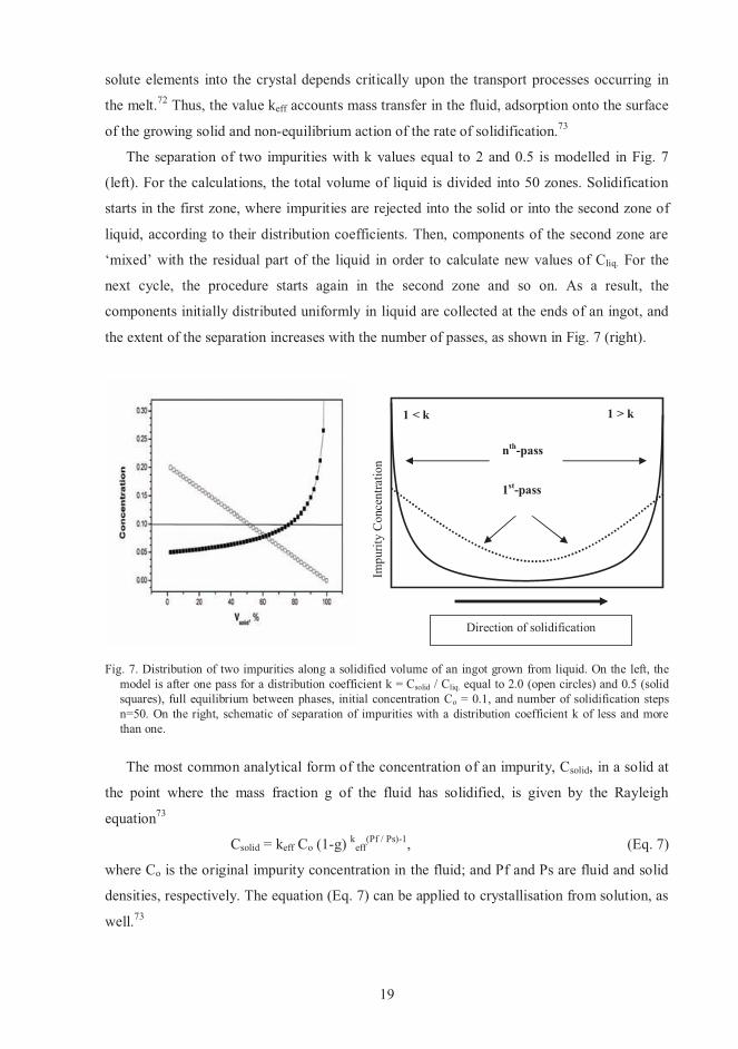
solute elements into the crystal depends critically upon the transport processes occurring in
the melt.72 Thus, the value keff accounts mass transfer in the fluid, adsorption onto the surface
of the growing solid and non-equilibrium action of the rate of solidification.73
The separation of two impurities with k values equal to 2 and 0.5 is modelled in Fig. 7
(left). For the calculations, the total volume of liquid is divided into 50 zones. Solidification
starts in the first zone, where impurities are rejected into the solid or into the second zone of
liquid, according to their distribution coefficients. Then, components of the second zone are
‘mixed’ with the residual part of the liquid in order to calculate new values of Cliq. For the
next cycle, the procedure starts again in the second zone and so on. As a result, the
components initially distributed uniformly in liquid are collected at the ends of an ingot, and
the extent of the separation increases with the number of passes, as shown in Fig. 7 (right).
Fig. 7. Distribution of two impurities along a solidified volume of an ingot grown from liquid. On the left, the model is after one pass for a distribution coefficient k = Csolid / Cliq. equal to 2.0 (open circles) and 0.5 (solid squares), full equilibrium between phases, initial concentration Co = 0.1, and number of solidification steps n=50. On the right, schematic of separation of impurities with a distribution coefficient k of less and more than one.
The most common analytical form of the concentration of an impurity, Csolid, in a solid at
the point where the mass fraction g of the fluid has solidified, is given by the Rayleigh
equation73
Csolid = keff Co (1-g) keff(Pf / Ps)-1, (Eq. 7)
where Co is the original impurity concentration in the fluid; and Pf and Ps are fluid and solid
densities, respectively. The equation (Eq. 7) can be applied to crystallisation from solution, as
well.73
Impu
rity
Con
cent
ratio
n
Direction of moving of solid-liquid f
1 > k 1 < k
nth-pass
1st-pass
Direction of solidification
20
A single crystal growth can be used for purification, since the well-formed crystal is
growing at equilibrium between solid-liquid phases, when keff is near the equilibrium value k.
The single crystal is less contaminated by impurities than, for example, the powder crystals.
This approach is widely used in Bridgman-Stockbarger51 and zone refinement techniques for
purification of TlBr from the molten state.
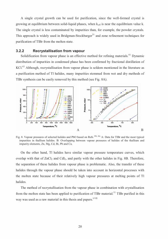
3.2.2 Recrystallisation from vapour Solidification from vapour phase is an effective method for refining materials.61 Dynamic
distribution of impurities in condensed phase has been confirmed by fractional distillation of
KCl.63 Although, recrystallisation from vapour phase is seldom mentioned in the literature as
a purification method of Tl halides, many impurities stemmed from wet and dry methods of
TlBr synthesis can be easily removed by this method (see Fig. 8A).
A B
Fig. 8. Vapour pressures of selected halides and PbO based on Refs.38b, 44e A: Data for TlBr and the most typical impurities in thallium halides. B: Overlapping between vapour pressures of halides of the thallium and impurity elements, Zn, Mg, Cd, Bi, Pb and Cu.
On the other hand, Tl halides have similar vapour pressure temperature curves, which
overlap with that of ZnCl2 and CdI2, and partly with the other halides in Fig. 8B. Therefore,
the separation of these halides from vapour phase is problematic. Also, the transfer of these
halides through the vapour phase should be taken into account in horizontal processes with
the molten state because of their relatively high vapour pressures at melting points of Tl
halides.
The method of recrystallisation from the vapour phase in combination with crystallisation
from the molten state has been applied to purification of TlBr material.51 TlBr purified in this
way was used as a raw material in this thesis and papers.I-VII

21
3.2.3 Recrystallisation from the molten state In purification methods based on recrystallisation from the molten state, the host material
serves as liquid solvent in the molten state and as solute in the solid state. Compatibility of
impurities with liquid and solid host is a factor for impurity distribution between phases.
Therefore, the radii of impurity ions and their oxidation states play a role in separation of
impurities during recrystallisation from the melt. Possibly the first work and modelling on this
topic was done in 1947, when rejection of K and Cu ions was studied during crystal growth of
NaCl.64 In alkali halide crystals, the enthalpy of mixing and anion environment of the first
coordination sphere were the primary parameters affecting the distribution coefficient of Cd2+,
which was calculated and measured (experimental data in parentheses) in NaF – 0.006
(0.007), NaCl – 0.014 (0.017), NaBr – 0.10 (0.09) and NaI – 0.38 (ND).65
Data on distribution coefficients of different elements in Tl halides are limited. Average
impurity distribution coefficients were found for TlCl and TlBr (in parenthesis) for the
following elements: Cu – 0.009 (0.006), Ag – 0.004 (0.006), Pb – 0.04 (0.05), S (sulphate) -
<1 (<1), O (Tl2O) - <1 (<1), Fe – <1 (ND), Cd - <1 (ND). It was mentioned that Tl2O moved
to the end of an ingot less effectively than a sulphate impurity.52a Distribution of Li, Ca, Cr,
Fe, Cu and Ba as impurities along a TlBr ingot purified by the zone refining technique was
studied using ICP-MS in the work of Oliveira et. al.66 From that data, the authors deduced
distribution coefficients for Li (0.161), Ba (0.284) and Cr (0.238).67
3.2.3.1 Bridgman-Stockbarger method In the Bridgman-Stockbarger method, the raw material is sealed into a quartz/glass
ampoule with the appropriate inert atmosphere or vacuum. The seed crystal is located at the
neck of the ampoule. A temperature stair with a gradient on the order of 10oC/cm or steeper is
created inside the vertical oven and the material inside ampoule passes several times from the
molten to the solid state, the seed being always in the cold part of the oven.74a
The Bridgman-Stockbarger method is often called ‘directed crystallisation’,51 when it is
used for purification with higher rate of crystallisation than is needed for single crystal
growth. The method can be used in horizontal setups as well. However, an optimal rate of
crystallisation for Tl halides was 3 mm/h (typical for single crystals) and the best purification
was obtained in vertical mode, which the authors explained as being due to the difference in
density between the melt and foreign particles.52a
The distribution of an impurity along the polycrystalline ingot for one pass is illustrated in
Fig. 9A, where water is collected by the melt and, therefore, is moved by the crystallisation
22
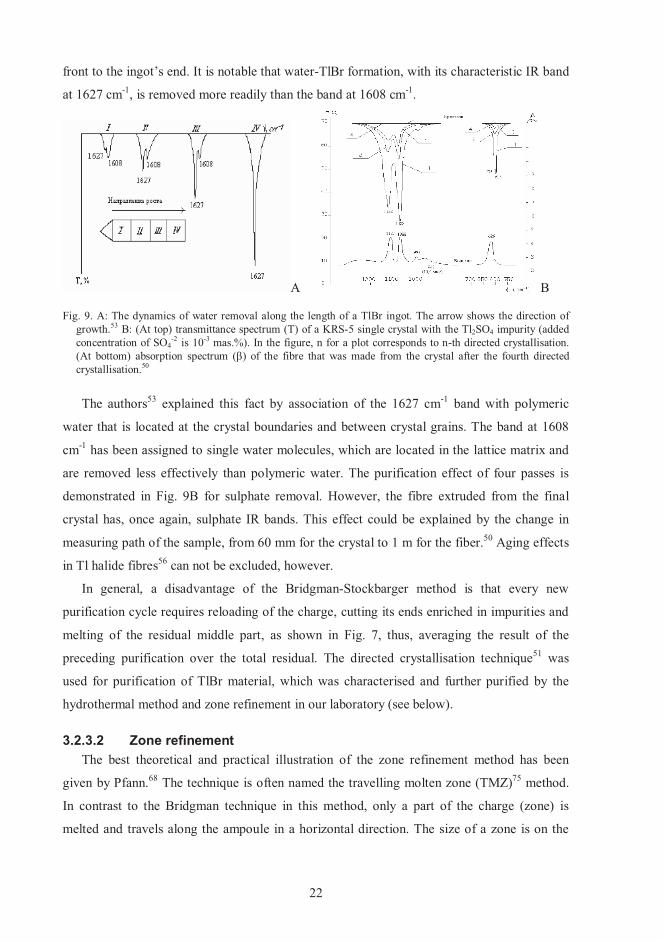
front to the ingot’s end. It is notable that water-TlBr formation, with its characteristic IR band
at 1627 cm-1, is removed more readily than the band at 1608 cm-1.
A B
Fig. 9. A: The dynamics of water removal along the length of a TlBr ingot. The arrow shows the direction of growth.53 B: (At top) transmittance spectrum (T) of a KRS-5 single crystal with the Tl2SO4 impurity (added concentration of SO4
-2 is 10-3 mas.%). In the figure, n for a plot corresponds to n-th directed crystallisation. (At bottom) absorption spectrum (�) of the fibre that was made from the crystal after the fourth directed crystallisation.50
The authors53 explained this fact by association of the 1627 cm-1 band with polymeric
water that is located at the crystal boundaries and between crystal grains. The band at 1608
cm-1 has been assigned to single water molecules, which are located in the lattice matrix and
are removed less effectively than polymeric water. The purification effect of four passes is
demonstrated in Fig. 9B for sulphate removal. However, the fibre extruded from the final
crystal has, once again, sulphate IR bands. This effect could be explained by the change in
measuring path of the sample, from 60 mm for the crystal to 1 m for the fiber.50 Aging effects
in Tl halide fibres56 can not be excluded, however.
In general, a disadvantage of the Bridgman-Stockbarger method is that every new
purification cycle requires reloading of the charge, cutting its ends enriched in impurities and
melting of the residual middle part, as shown in Fig. 7, thus, averaging the result of the
preceding purification over the total residual. The directed crystallisation technique51 was
used for purification of TlBr material, which was characterised and further purified by the
hydrothermal method and zone refinement in our laboratory (see below).
3.2.3.2 Zone refinement The best theoretical and practical illustration of the zone refinement method has been
given by Pfann.68 The technique is often named the travelling molten zone (TMZ)75 method.
In contrast to the Bridgman technique in this method, only a part of the charge (zone) is
melted and travels along the ampoule in a horizontal direction. The size of a zone is on the
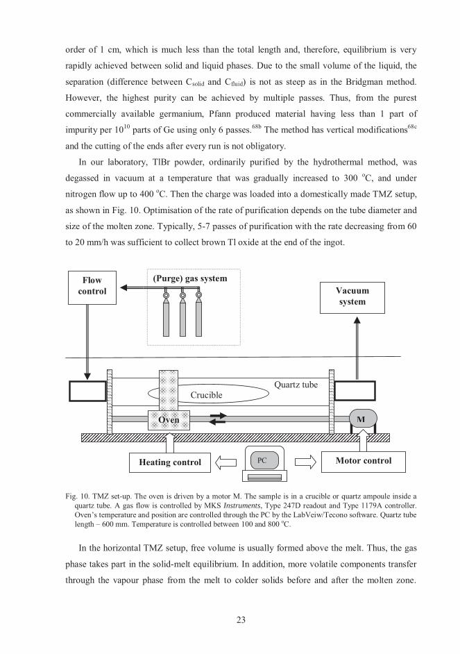
23
order of 1 cm, which is much less than the total length and, therefore, equilibrium is very
rapidly achieved between solid and liquid phases. Due to the small volume of the liquid, the
separation (difference between Csolid and Cfluid) is not as steep as in the Bridgman method.
However, the highest purity can be achieved by multiple passes. Thus, from the purest
commercially available germanium, Pfann produced material having less than 1 part of
impurity per 1010 parts of Ge using only 6 passes.68b The method has vertical modifications68c
and the cutting of the ends after every run is not obligatory.
In our laboratory, TlBr powder, ordinarily purified by the hydrothermal method, was
degassed in vacuum at a temperature that was gradually increased to 300 oC, and under
nitrogen flow up to 400 oC. Then the charge was loaded into a domestically made TMZ setup,
as shown in Fig. 10. Optimisation of the rate of purification depends on the tube diameter and
size of the molten zone. Typically, 5-7 passes of purification with the rate decreasing from 60
to 20 mm/h was sufficient to collect brown Tl oxide at the end of the ingot.
Fig. 10. TMZ set-up. The oven is driven by a motor M. The sample is in a crucible or quartz ampoule inside a quartz tube. A gas flow is controlled by MKS Instruments, Type 247D readout and Type 1179A controller. Oven’s temperature and position are controlled through the PC by the LabVeiw/Tecono software. Quartz tube length – 600 mm. Temperature is controlled between 100 and 800 oC.
In the horizontal TMZ setup, free volume is usually formed above the melt. Thus, the gas
phase takes part in the solid-melt equilibrium. In addition, more volatile components transfer
through the vapour phase from the melt to colder solids before and after the molten zone.
MOven
Crucible
Motor control PCHeating control
Vacuum system
Flow control
(Purge) gas system
Quartz tube
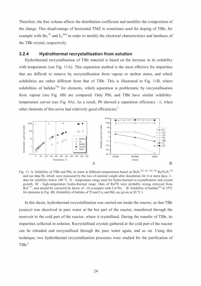
24
Therefore, the free volume affects the distribution coefficient and modifies the composition of
the charge. This disadvantage of horizontal TMZ is sometimes used for doping of TlBr, for
example with Br276 and I2,44a in order to modify the electrical characteristics and hardness of
the TlBr crystal, respectively.
3.2.4 Hydrothermal recrystallisation from solution Hydrothermal recrystallisation of TlBr material is based on the increase in its solubility
with temperature (see Fig. 11A). This separation method is the most effective for impurities
that are difficult to remove by recrystallisation from vapour or molten states, and which
solubilities are rather different from that of TlBr. This is illustrated in Fig. 11B, where
solubilities of halides34a for elements, which separation is problematic by recrystallisation
from vapour (see Fig. 8B) are compared. Only PbI2 and TlBr have similar solubility-
temperature curves (see Fig. 8A). As a result, Pb showed a separation efficiency ~1, when
other elements of this series had relatively good efficiencies.I
A B
Fig. 11. A: Solubility of TlBr and PbI2 in water at different temperatures based on Refs,38a, 38c, 34f, 52b Ref7a/b,100
and our data Ht, which were measured by the loss of nutrient weight after dissolution for 4 or more days. I - data for solubility below 100 oC. II - temperature range used for hydro-thermal re-crystallisation and crystal growth. III - high-temperature hydro-thermal range. Data of Ref7b were probably wrong retrieved from Ref.177, and should be corrected by factor of ~10 (compare with Cor7b). B: Solubility of halides34a at 25oCfor elements in Fig. 8B. (Solubility of halides of Tl and Cu, and BiI3 are given at 20 oC.)
In this thesis, hydrothermal recrystallisation was carried out inside the reactor, so that TlBr
(source) was dissolved in pure water at the hot part of the reactor, transferred through the
reservoir to the cold part of the reactor, where it crystallised. During the transfer of TlBr, its
impurities collected in solution. Recrystallised crystals gathered at the cold part of the reactor
can be reloaded and recrystallised through the pure water again, and so on. Using this
technique, two hydrothermal recrystallisation processes were studied for the purification of
TlBr.I

25
During the first process shown in Fig. 6 a small amount of TlBr was totally dissolved at
hydrothermal conditions. Recrystallised crystals were formed by cooling of the solution. In
the second recrystallisation process a large amount of TlBr was transferred through the pure
water due to the temperature gradient inside the reactor. The ratio of amounts of material in
the second to the first process was ~10. Based on trace element analysis, the degree of
purification obtained from the process was evaluated for separate element by the ratio of its
concentrations before and after the process.I The efficiency of the overall process can be
evaluated based on the ratio of the sums of concentrations of all elements. Evaluated in this
way, the average purity of TlBr was improved by a factor of ~4 in the first process and by a
factor of ~2 in the second process.
3.2.5 Combination of purification methods The combination of purification methods allows acceleration of the refining process. For
example, a sequence using distillation and solidification from melt has been used for
purification of alkali halides63 and Tl halides.51 The efficiency of using a combination of
different methods can be illustrated by Cl- and I- anions, which are hardly removed from TlBr
during crystallisation, whether from the molten state or from vapour. Thallium halides have
similar characters in molten and solid state, and easily form solid solutions with each other.44a
These compounds have similar vapour pressure temperature curves, and therefore their
separation from vapour phase is also problematic (see Fig. 8B). On the other hand, solubilities
of TlCl and TlI are one order of magnitude greater and one order of magnitude less,
respectively, than that of TlBr (see Table 2 and Fig. 11B). Therefore, during the
recrystallisation of TlBr from water solutions, TlCl dissolves and remains in the solution, and
TlI stays undissolved.
In this thesis, a combination of purification methods was applied to TlBr material, which
was purified by 5-7 cycles of distillation and solidification from melt. Then, a single crystal
was grown by the Bridgman method. This single crystal was hydrothermally recrystallised by
dissolving it in pure water, then 5 purification runs were done using TMZ.
This sequence of purification steps and further crystal growth supplied the crystal with the
mobility-lifetime product (μ�) estimated as 3.3x10⁻⁴ cm2/V (for electrons).77 This value was
one order of magnitude better than the value 3x10⁻⁵ cm2 V-1, which was obtained by Olschner
et. al.,6 for 200-300 passes of a molten zone.

26
3.3 Crystal growth Crystal growth is an attractive subject for many researchers. It is an art and a science,78 a
laboratory practice79 and an industry technique.80 The growth can be done from solutions,81
liquids,82 melts,83 high-temperature solutions84 and in gels.85 One of the best classifications of
crystal growth methods is based on the medium from which the growth is carried out.86 Thus,
there are techniques for crystal growth from melt, vapour and solution.
3.3.1 Crystal perfection Temperature has a primary effect on the quality of the growing crystal due to the entropy
disordering factor S(->max):
G(->min) = H(->min) – T S(->max). (Eq. 8)
The process of crystal structure formation (ordering) is characterised by the minimisation of
enthalpy H and the minimum total gain in Gibbs free energy (G).87a Thus, ordering and
disordering forces contribute to different extents to the process of crystallisation, resulting in
the incorporation of point defects into the lattice:
nmin = N exp(-Ed / kT), (Eq. 9)
where N is the total number of possible sites, Ed is defect formation energy and nmin is
minimum (or more) number of defects, the so-called perfection limit. The value nmin for TlBr
plotted in Fig. 12 is about one order of magnitude higher for Schottky than for Frenkel point
defects, although the latter should be corrected by the factor �nis, where nis is the total number
of interstitial positions.87a The probability of defect formation by the Frenkel mechanism is
low at low temperatures because the Tl halides have ionic radius ratios of cation to anion
(Rc/Ra) close to the stability limit value88 of 0.732 for CsCl-type structure: 0.878, 0.811 and
0.723 for TlCl, TlBr and TlI, respectively. So the CsCl-type structure becomes stable for Tl
iodide only at temperatures higher than 168 oC (see Table 2).
During crystallisation at high temperatures a certain fraction of defects is frozen into the
lattice due to the limitation of the diffusion rate.87a Thus, the plots in Fig. 12 determine the
thermodynamic limits of defect concentration according to the crystal growth temperature.
For example, accordingly to the Schottky defect values, the growth from solution at 100oC
and 200oC is 40 000 and 400 times, respectively, more preferable than growth from melt.
However, no crystal growth method for TlBr approaches the perfection limit due to the
properties of TlBr and techniques used.
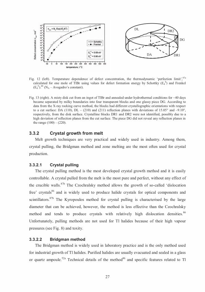
27
Fig. 12 (left). Temperature dependence of defect concentration, the thermodynamic ‘perfection limit’,87a
calculated for one mole of TlBr using values for defect formation energy by Schottky (EdS) and Frenkel
(EdF).89 (NA – Avogadro’s constant).
Fig. 13 (right). A misty disk cut from an ingot of TlBr and annealed under hydrothermal conditions for ~40 days became separated by milky boundaries into four transparent blocks and one glassy piece DG. According to data from the X-ray rocking curve method, the blocks had different crystallographic orientations with respect to a cut surface: DA (110), DL – (210) and (211) reflection planes with deviations of 15.05� and –9.10�,respectively, from the disk surface. Crystalline blocks DR1 and DR2 were not identified, possibly due to a high deviation of reflection planes from the cut surface. The piece DG did not reveal any reflection planes in the range (100) – (220).
3.3.2 Crystal growth from melt Melt growth techniques are very practical and widely used in industry. Among them,
crystal pulling, the Bridgman method and zone melting are the most often used for crystal
production.
3.3.2.1 Crystal pulling The crystal pulling method is the most developed crystal growth method and it is easily
controllable. A crystal pulled from the melt is the most pure and perfect, without any effect of
the crucible walls.87b The Czochralsky method allows the growth of so-called ‘dislocation
free’ crystals86 and is widely used to produce halide crystals for optical components and
scintillators.87b The Kyropoulos method for crystal pulling is characterised by the large
diameter that can be achieved, however, the method is less effective than the Czochralsky
method and tends to produce crystals with relatively high dislocation densities.86
Unfortunately, pulling methods are not used for Tl halides because of their high vapour
pressures (see Fig. 8) and toxity.
3.3.2.2 Bridgman method The Bridgman method is widely used in laboratory practice and is the only method used
for industrial growth of Tl halides. Purified halides are usually evacuated and sealed in a glass
or quartz ampoule.52a Technical details of the method86 and specific features related to Tl
DA DR1
DL DR2
DG

28
halides51 are well described. The growth rate depends on the minimum crystal dimension L as
1/ Ln, where n is between 1 and 2. For L~10 mm, rates are usually in the range of 1–10 mm/h,
the values being larger for materials with higher thermal conductivity.86 Several
disadvantages of the method, however, are summarised below.
Many problems with the Bridgman method stem from the direct contact between the
crystal and the crucible material.87b Adhesion and differences in thermal expansion
coefficients produce stress in the growing crystal and initiate secondary grain nucleation on
crucible walls,37 resulting in the formation of separate crystals inside the ingot,20 as shown in
Fig. 13 for TlBr. Secondary nucleation and twinning can be minimised by the use of a
horizontal method.86 However, the extraction of the grown crystal from the crucible may
result in its cracking.87b
The second problem is connected with purity requirements. The crucible selected must be
appropriate and not produce contamination.86 In the Bridgman method, impurity distribution
is not uniform along the growing ingot (see in Fig. 7) and the problem is made worse by
insufficient mixing in the molten zone.87b
The next problem is to obtain and maintain the desired temperature distribution. Thermal
conductivity of the crucible should be less than that of the material grown.86 Temperature
gradients before the crystallisation front are responsible for the radial non-uniformity of a
crystal, twinning and seed formation. The temperature in the liquid in front of the crystallising
face is often locally increased by about 60 degrees51 in order to improve solid-liquid
equilibration by means of convectional mixing of the liquid. But this operation considerably
increases the temperature gradient between solid-liquid phases, and creates laminar liquid
flows that result in additional tensions in the cooling crystal. Defects, impurities and
imperfections are more quickly frozen into the crystal lattice and number of defects in the
lattice becomes further away from the perfection limit (Eq. 9).
In Fig. 14, the single crystal of TlBr is grown without the formation of separate crystals
shown in Fig. 13. However, the irregular distribution of temperature, cooling tensions in the
crystal and tensions stemming from the walls of the crucible result in strain and non-
uniformity in the single crystal. Non-uniform zones can also be revealed by etching.III It
should be noted that cutting and polishing effects are involved as well.
In general, non-uniformity in the Bridgman method originates from temperature gradients
during the crystallisation and from the walls of the crucible during cooling. Adhesion of the
crystal to the crucible material creates additional problems with blocking and cracking of the
ingot. Recent attempts to decrease the adhesion and improve the crystallisation front shape
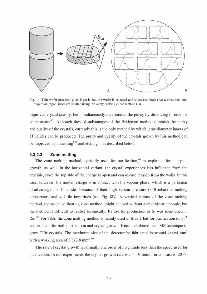
29
A B
Fig. 14. TlBr wafer processing: an ingot is cut, the wafer is oriented and slices are made (A); a cross-sectional map of an ingot: slices are studied using the X-ray rocking curve method (B).
improved crystal quality, but simultaneously deteriorated the purity by dissolving of crucible
components.VII Although these disadvantages of the Bridgman method diminish the purity
and quality of the crystals, currently this is the only method by which large diameter ingots of
Tl halides can be produced. The purity and quality of the crystals grown by this method can
be improved by annealingI, II and etching,III as described below.
3.3.2.3 Zone melting The zone melting method, typically used for purification,68 is exploited for a crystal
growth, as well. In the horizontal variant, the crystal experiences less influence from the
crucible, since the top side of the charge is open and can release tension from the walls. In this
case, however, the molten charge is in contact with the vapour phase, which is a particular
disadvantage for Tl halides because of their high vapour pressure (~10 mbar) at melting
temperature and volatile impurities (see Fig. 8B). A vertical variant of the zone melting
method, the so-called floating zone method, might be used without a crucible or ampoule, but
the method is difficult to realise technically. Its use for production of Si was mentioned in
Ref.86 For TlBr, the zone melting method is mainly used in Brazil, but for purification only,66
and in Japan for both purification and crystal growth. Hitomi exploited the TMZ technique to
grow TlBr crystals. The maximum size of the detector he fabricated is around 4x4x4 mm3
with a working area of 3.8x3.8 mm2.90
The rate of crystal growth is normally one order of magnitude less than the speed used for
purification. In our experiments the crystal growth rate was 5-10 mm/h, in contrast to 20-60
M13(1)4(2)Set22
Sqrt
(Cou
nts
)
0
1 0
1 00
2 00
3 00
4 00
5 00
6 00
7 00
8 00
9 00
1 000
1 100
1 2001 3001 4001 500
1 6001 7001 8001 900
Thet a - Sca le
6.2 7 8 9 10
11 12 13
14 15 16
17
Thet a - Sca le
6.2 7 8 9 1 0 11 1 2 13 1 4 15 1 6 17
Set22
M13(1)4(1) Set22
Sqrt
(Cou
nts
)
01
1 0
1 00
2 00
3 00
4 00
5 00
6 00
7 00
8 00
9 00
1 000
1 100
1 200
1 300
Thet a - Sca le
5.7 6 7 8 9 10 11
12
13 14 15
16 17
Thet a - Sca le
5.7 6 7 8 9 10 1 1 12 1 3 14 1 5 16 1 7
Set2 2
M13(1)3(3) Set45
Sqrt
(Cou
nts
)
0
1 0
1 00
2 00
3 00
4 00
5 00
6 00
7 00
8 00
9 00
1 000
1 100
1 2001 300
1 4001 5001 6001 7001 800
Thet a - Sca le
9 10 11 12
13
14 15 16
17 18 19 20
Thet a - Sca le
9 10 1 1 12 1 3 14 15 16 1 7 18 1 9 20
set4 5
M13(1)3(2) Set45new
Sqrt
(Cou
nts
)
0
1 0
1 00
1 000
2 00
3 00
4 00
5 00
6 00
2 000
Thet a - Sca le
8 9 10
11 12
13 14 15 16 17
18 19
Thet a - Sca le
8 9 10 1 1 12 1 3 14 1 5 16 1 7 18 19
M13( 1) 3(2) Set45 new
M13(1)3(1)Set67
Sqrt
(Cou
nts
)
0
1 0
1 00
2 00
3 00
4 00
5 00
6 00
7 00
8 00
9 00
1 000
1 100
1 200
1 3001 400
1 5001 600
Thet a - Sca le
5.1 6 7 8 9 10 11
12 13 14
15 16
17
Thet a - Sca le
5.1 6 7 8 9 10 11 12 1 3 14 15 16 17
Set67
M13(1)2(3) Set22
Sqrt
(Cou
nts
)
01
1 0
1 00
2 00
3 00
4 00
5 00
6 00
7 00
8 00
9 00
1 000
1 100
1 200
Thet a - Sca le
7.6 8 9 10 11
12
13 14 15 16 17
18
19
Thet a - Sca le
7.6 8 9 1 0 11 12 13 14 1 5 16 17 1 8 19
Set2 2
M13(1)2(2) Set45
Sqrt
(Cou
nts
)
01
1 0
1 00
2 00
3 00
4 00
5 00
6 00
7 00
8 00
9 00
1 000
1 100
1 200
1 300
1 400
Thet a - Sca le
9.1
10
11 12 13 14 15
16
17 18 19 20
Thet a - Sca le
9.1 10 11 12 13 14 1 5 16 1 7 18 1 9 20
Set 45
M13(1)2(1)Set67
Sqrt
(Cou
nts
)
0
1
1 0
1 00
2 00
3 00
4 00
5 00
6 00
7 00
8 00
9 00
1 000
1 100
Thet a - Sca le
3.1 4 5 6 7 8 9 10
11
12
13
14
Thet a - Sca le
3.1 4 5 6 7 8 9 10 11 1 2 13 14
Set 67
M13(1)1(2)set00
Sqrt
(Cou
nts
)
0
1
1 0
1 00
2 00
3 00
4 00
5 00
6 00
7 00
8 00
9 00
1 000
Thet a - Sca le
13.2
14 15 16
17 18 19 20
21 22 23 24
25
Thet a - Sca le
13.2 1 4 15 1 6 17 1 8 19 2 0 21 2 2 23 2 4 25
Set0 0
M13(1)1(1) Set45
Sqrt
(Cou
nts
)
0
1
1 0
1 00
2 0
3 0
4 05 06 0
2 00
3 00
4 00
5 00
6 00
Thet a - Sca le
10.2
11
12 13 14
15 16 17
18 19 20 21
22
Thet a - Sca le
1 0.2 11 1 2 13 1 4 15 1 6 17 18 1 9 20 21 22
Set 45

30
mm/h used for purification. The maximum size of a detector fabricated in our laboratory was
around 7x6x4 mm3 with an electrode diameter of 3 mm.77
The smaller diameter of ingots grown by TMZ in comparison with the Bridgman method
is a current disadvantage for TMZ. However, application of the floating zone method and
development of a narrow zone heater might improve the purity and crystal quality of the TlBr
to the extent that the total cross section of an ingot would be available for detector fabrication.
This is supported by recent successful fabrication of a 4-mm detector77, VI and possibility to
grow the ingot of high quality (see Fig. 29A) that is lower than industrial Si only by factor 3
(intensity: 34 vs 90 Kcnts; FWHM: 0.094 vs 0.034).178
3.3.3 Crystal growth from vapour In general, crystal growth from vapour is more easily treated theoretically than crystal
growth from a condense phase, since vapour comes more quickly than a fluid into equilibrium
with a solid and the role of intermolecular forces in gas phase is negligible.91 Crystals grown
by this method should be free of effects from the crucible walls. For Tl halides, vapour
growth is used for purification.61, 51 There are no reports in the literature of growth of Tl
halide single crystals from gas phase, possibly due to the lower productivity of this method in
comparison with crystal growth from the melt.
However, the method is used for the production of Tl halide films. Kondo et al. have
produced uniform amorphous TlBr101 and TlCl92 films condensed from gas phase on a
metallic surface at cryogenic temperature, and they observed a well-defined transformation to
crystalline phase at low temperatures. These films are clear and, therefore, the effect of
crystallisation on their optical absorption near the UV fundamental edge has been studied.93 In
TlCl1-xBrx films, crystallisation is affected by chemical disorder, as shown by UV absorption
measurements.94 A method for preparation of uniform amorphous films of mixed metal
halides by means of two-source evaporation was recently described.95 The thin films have a
thickness of 300-500 nm and could be utilised for UV and soft X-ray detection.
In this work, condensation of TlBr vapour was studied on an Al surface heated to above
room temperature. At temperatures below 150 oC, the crystalline films formed were uniform
and transparent. If a sample was under a temperature gradient, the film had a thickness
gradient that monotonically followed the temperature gradient of the substrate.
At temperatures above 150 oC, metallic Tl drops formed on Al surface that was confirmed
by microscope and XRD studies. The corresponding reaction could be written as follows:
Al (metal) + 3 TlBr (g) = AlBr3 (g) + 3 Tl (dispersion) (Eq. 10)
31
with �G = -44.4 kcal at 150 oC.57 The �G of this reaction becomes positive only at
temperature above 900 oC, but the reaction below 150 oC is possibly inhibited by an Al oxide
film on its surface. The �G of the reaction between the Al oxide and TlBr, given as follows:
Al2O3 + 6 TlBr(g) = 2 AlBr3(g) + 3 Tl2O, (Eq. 11)
has reasonably positive values (184.6 kcal at 150 oC57). On the other hand, the reaction (Eq.
10) is ‘accelerated’ by AlBr3, which easily escapes from the reaction zone because of its high
vapour pressure, which is about 40 mm of Hg at 150 oC.38b
TlBr films grown from vapour on an Al surface are no thicker than ~500 nm. Prolonged
growth results in the formation of an opaque polycrystalline layer on the Al surface. In
general, the deposition of TlBr from the gas phase onto various metals is a useful technique
for making TlBr (film) – metal interfaces.
3.3.4 Growth from solution Solution growth techniques are attractive because of the low ‘perfection limit’ (see Fig.
12) and ‘freedom’ of the growth (compare with effects of crucible walls in the Bridgman
method, Fig. 13 and Fig. 14B). Based on temperature and pressure used, the solution growth
methods are conventionally divided into the low-temperature, hydrothermal and high-
temperature methods. The first two are used in this work and discussed below. The high
temperature method is sometimes called ‘flux growth’, because high temperature melts of
salts are used as solvents. There are a few Tl halide – nitrate systems,96 where the solubility of
the halides is comparable to that in water. Liquid-phase epitaxy and electrolysis are typical
solution methods.86 Liquid-phase epitaxy has not been used for TlBr, whereas the formation
of TlBr adlayers was observed and studied on Au, Ag and Pt electrodes.97, 98, 99 Growth from
gel can also be a promising method, since Tl iodide crystals with a size of ~1 mm grown by
this method have been reported.85
A subsystem for classification of solution growth methods is often based on the method
for achieving supersaturation of the solution: cooling, temperature gradient and solvent
evaporation. The last technique is not suitable for Tl halides, since they are sparingly
dissolved in water at room temperature, and therefore the productivity of this method is low.
Solubility is a necessary attribute for crystal growth by a solution method. The solubility
of TlBr in water increases considerably with temperature: it is only 0.05% at 20 �C, 0.5% at
~94 oC and it is already about 5 % at 250 oC. The plot of solubility in Fig. 11A is divided in
three parts: a low-temperature area below 100 �C (I) and a hydrothermal area with stable (II)
and unstable (III) crystal growth of TlBr.
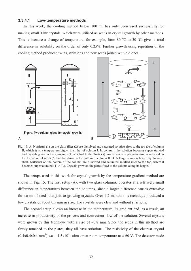
32
3.3.4.1 Low-temperature methods In this work, the cooling method below 100 �C has only been used successfully for
making small TlBr crystals, which were utilised as seeds in crystal growth by other methods.
This is because a change of temperature, for example, from 80 oC to 30 oC, gives a total
difference in solubility on the order of only 0.25%. Further growth using repetition of the
cooling method produced twins, striations and new seeds joined with old ones.
A B
Fig. 15. A: Nutrients (1) on the glass filter (2) are dissolved and saturated solution rises to the top (3) of column II, which is at a temperature higher than that of column I. In column I the solution becomes supersaturated and crystals grow on the glass rods (4) attached to the floats (5). An excess of super-saturation is released on the formation of seeds (6) that fall down to the bottom of column II. B: A long column is heated by the outer shell. Nutrients on the bottom of the column are dissolved and saturated solution rises to the top, where it becomes supersaturated (T2 > T1). Crystals grow on the plates fixed to the column along its length.
The setups used in this work for crystal growth by the temperature gradient method are
shown in Fig. 15. The first setup (A), with two glass columns, operates at a relatively small
difference in temperatures between the columns, since a larger difference causes extensive
formation of seeds that join to growing crystals. Over 1-2 months this technique produced a
few crystals of about 0.5 mm in size. The crystals were clear and without striations.
The second setup allows an increase in the temperature, its gradient and, as a result, an
increase in productivity of the process and convection flow of the solution. Several crystals
were grown by this technique with a size of ~0.8 mm. Since the seeds in this method are
firmly attached to the plates, they all have striations. The resistivity of the clearest crystal
(0.4x0.4x0.4 mm3) was ~1.5x10¹¹ ohm�cm at room temperature at ± 60 V. The detector made
T1
T2
33
from this crystal by Bruker Baltic (Latvia) can resolve all necessary spectral lines, however its
spectral characteristics are unstable.
3.3.4.2 Hydrothermal growth The hydrothermal method allows water, high temperature and pressure to produce effects
that are not attainable under ambient condition. The Earth itself is a huge high pressure and
high temperature vessel,102 in which diamonds, quartz and other crystalline minerals are
synthesised and grown. A comprehensive review on the hydrothermal formation of silicates
was published already in 1913.103 Complete information on pressure-volume-temperature
relations in water was given by Kennedy104 in 1950. In this work, hydrothermal bombs were
used in order to increase the solubility of TlBr above 100 oC. Maximum values of pressure
and temperature were limited by the properties of the used bomb to ~ 25 bars and 225 oC at a
bomb filling of ~60%.
Cooling and temperature gradient methods were used for achieving supersaturation of the
solution. The seeds were placed on the levels above the solution, and after dissolving the
nutrient and approaching the equilibrium state (for ~4-6 days) the bomb was inverted from
top to bottom. Alternatively, overheating and cooling to the required temperature were used
for seed formation. As shown in Fig. 11A, the optimal temperature range for crystal formation
and growth was zone II, which is between 100 – 190 oC, since at higher temperatures the
crystals grew easily with rounded shapes and faces, resembling more closely clear icicles than
well shaped crystals. Also, the crystal quality of the ‘icicles’ was too low to create x-ray
diffraction reflections. All crystals grown by the temperature gradient method had a large
number of striations, like crystals grown at the low temperatures in Fig. 15B. Therefore, the
method was used for recrystallisation (purification) purposes.
Crystals of better quality were grown from solution during prolonged crystal growth by
the hydrothermal cooling method. In a typical example, saturated solution at 200 �C was
slowly cooled to 180 oC, in order to form seeds and achieve supersaturation. Then prolonged
cooling to 140 oC was done over the course of 40 days. At these conditions the concentration
of TlBr changed from 2.3% to 1.1%, and the crystals grew to ~1 mm size and more.
Unfortunately, the repetition of this technique gave striations on the crystals, or crystals that
were joined, or crystals that looked like stairways. One of the crystals grown by this method
(3x3x0.4 mm3) had a resistivity of ~1.5x10¹¹ ohm�cm at room temperature at +70 V. The
detector made by Bruker Baltic from this crystal was able to count gamma-ray photons, but
not to resolve, all spectral lines.
34
3.4 Annealing Single crystals of TlBr grown from the molten state by the Bridgman method (chapter
3.3.2.2) are strained basically due to the effects of the crucible walls and the cooling regime.
The applied stress easily generates dislocations in the cooling crystal. The motion of
dislocation in shear (like the motion of a vacancy) is the movement of a corresponding line of
atoms for only one interatomic distance or less. Thus, the stress required to move a
dislocation is several orders of magnitude smaller than the stress required to shear one entire
plane of atoms simultaneously over another in a perfect crystal.105 The different dislocations
accumulated during cold work create stress fields that interact strongly and lock the
dislocations into metastable configurations. The crystal becomes harder, and externally
applied stress should be sufficient to make dislocations move through the opposing stress
fields of other dislocations.105 The crystal has gained extra free energy from the work done on
it. Metastable configurations undergo spontaneous changes to reduce the extra free energy,
which is reflected, for example, in strain aging.106
Besides hardening, other properties, such as resistivity and rate of dissolution, are changed
in worked material.107 The broadening of X-ray diffraction lines in strained material has long
been the only method for the study of worked material and its annealing on the micro-scale
level. Annealing removes strains, improves the quality of the crystal and restores the
properties of the material.106 Annealing has a clearing effect on opaque crystals, shown for
TlBr in Fig. 13, where the hidden block structure of an ingot becomes visible. In this thesis,
effects of hydrothermal as well as various other annealing conditions on TlBr properties were
studied in papers I – III.
3.4.1 Types of annealing Annealing is known from ancient times and is widely associated with a heat treatment of a
worked material in order to make it softer. In general, the process consists of heating the
material to a definite temperature, keeping it at this temperature for the required time and
cooling at a controlled rate. Sometimes annealing includes a thermo-treatment with the use of
additional mechanical action. The result of the process is evaluated by measuring the
materials or by observation under a microscope. During the last hundred years, development
of X-ray diffraction methods has allowed the detection of fine effects of annealing and, thus,
insights into its mechanism.106 As a result, an understanding of the mechanisms of the
annealing process became possible on the microscopic level. The action of annealing depends

35
on applied stress and the temperature regime. Both these factors can be used to differentiate
the following types of annealing processes.106
Recrystallisation, or primary recrystallisation, is a process in which new crystals grow
from nuclei and replace the strained ones. The orientations of these new crystals are
independent of the strained crystals. Therefore, the growth is incoherent and results in the
advance of large-angle boundaries separating the new crystals from their surroundings.106
When the growing crystals have consumed all the strained material, they continue to grow
by consuming each other; this process is called grain growth. In specimens that have already
undergone primary recrystallisation after severe cold working, secondary recrystallisation
takes place at a higher temperature. During this recrystallisation a few grains grow
abnormally rapidly and become many times larger than the average grain.106
Thus, recrystallisation is associated with large-angle boundaries and, in general, is
observed to take place in a temperature range of 50 – 80 % of the melting temperature (Tmelt
K) of the material.108 For example, for TlBr (Tmelt = 733 K), this interval corresponds to 94 –
313 oC. In highly stressed KRS-5 material (Tmelt = 683 K) made by extrusion to fibres, grain
growth occurs with annealing above 50 oC,47 which corresponds to 47% of T melt.
Worked crystals can be repaired by the recovery process, preserving the orientation of the
crystal without its recrystallisation. The structure of the material, the annealing temperature
and the deformation type have primary effects on the recovery procedure. In cubic metals,
recovery usually only partly removes the work hardening, while hexagonal metal crystals
deformed in tension by basal slip can recover their original softness completely and do not
recrystallised.106 In general, recovery takes place at lower temperatures than recrystallisation.
Since point defects (vacancies) are more mobile than dislocations, their role is more important
at lower temperatures.107 At higher temperature, appreciable diffusion occurs and allows the
dislocations to move into a configuration of lower energy. Several dislocations will come
together and annihilate one another or combine to form a single dislocation.105 The energy per
dislocation in a grain boundary is less than for isolated dislocations, therefore, the excess free
energy of grain boundaries should be a driving force for crystallisation.86
The mechanism of dislocation movement and its elimination is explained by so-called the
strain-induced boundary migration. The boundary, present initially in a lightly worked grain,
migrates and causes the volume of material swept by it to become a strain-free continuation of
the grain from which the boundary originated. The orientation of a strained crystal varies
from point to point and so the strain-free additions which grow at different places along its
36
boundary have slightly different orientations from one another. As a result, when they join
together small-angle boundaries are formed between them.106
Because various crystal imperfections affect to a different extent the properties of
materials, the recovery of different properties with temperature occurs to different degrees and
non-simultaneously. Non-completeness of a recovery is often reflected in its definition as the
process of decreasing the amount and changing the distribution of point defects and
dislocations.107 In general, the recovery process is characterised by small-angle boundaries
and lower temperatures than recrystallisation.106 Therefore for TlBr, the recovery process can
be observed at room temperature.
The process of polygonisation was first studied on bent single crystals of Zn, Al, Mg and
NaCl. This process is characterised by small-angle grain boundaries and takes place in bent
crystals at temperatures well above that at which the material softens. A bent crystal contains
the excess edge dislocations of one sign106 that are more or less uniformly distributed on
parallel slip planes. In the process of annealing, dislocations on different slip lines line up one
above the other and form a small-angle grain boundary. The energy per dislocation is reduced
when the dislocations are so arranged.105
Polygonisation has features similar to recrystallisation in terms of the temperature, at
which it can occur, and it is similar to the recovery process in the terms of the small-angle
grain boundaries. However, polygonisation takes place only in bent crystals. In Tl halide
ingots grown by the Bridgman method, there are several points on the cylindrical surface
which are stuck to the walls of the crucible. The contraction forces create bent fields in 3D-
space during ingot cooling. Thus, polygonisation can take place throughout the annealing of
Tl halide crystals.
3.4.2 Processes associated with annealing The variety of annealing processes based on applying mechanical stress and heat
separately is enlarged by their combination, and/or by changing the environmental conditions
(gas medium or solution), or by operation of external forces (for example, electric fields).
3.4.2.1 Strain-anneal method A modification of the recrystallisation method as a strain-anneal method is used for so-
called solid-phase crystal growth (compare with strain-induced boundary migration, above)
The idea behind the method is to make the re-growth occurs inside the bulk of the material
during annealing so that the inner single crystal experiences minimum contamination from
crucible material and/or a reactive atmosphere. The material is heated to about half the

37
absolute melting temperature, where it is not brittle. Then, the material is subjected to strain
on the order of 1 - 10%. Annealing is carried out in a temperature range of 50 – 95 % of T melt,
a temperature gradient across the sample being considered an advantage. The rates of growth
are usually fast: 5 - 50 mm/h can be expected. The driving force for the process is the excess
free energy attributed to dislocations or clusters of dislocations and grain boundaries.86
3.4.2.2 Annealing of amorphous materials A solid in an amorphous (glassy) state has a higher free energy than in the form of a single
crystal. Solid-phase crystal growth is the crystallisation of glassy material that can be
accelerated by heating. The amorphous material is obtained, for example, from melt with a
high temperature gradient by rapid quenching. The method used for production of films is
known as solid-phase epitaxy. In films, selective crystallisation can be induced. Due to the
amorphous starting state, the highest doping densities can be achieved by this method.86
In Tl halides, crystallisation from an amorphous state in films occurs at low temperatures.
The amorphous phase is obtained on the substrate, which is kept at the temperature of liquid
nitrogen or oxygen. During heating, the crystallisation observed by optical absorption
spectroscopy takes place in a narrow temperature interval, near 95 K for TlBr,101 99 K for
TlCl,92 120 K for TlI93 and 138 K (maximum) for a mixture of TlCl (60 %) and TlBr (40%).94
According to an electron diffraction study both, a normal structure of CsCl-type and abnormal
structure of NaCl-type (rocksalt), were observed in TlBr and TlCl during heating. However,
the abnormal structure disappeared well before room temperature was reached.109
3.4.2.3 Effects of impurities During annealing, impurities are attracted to the region of tension around a dislocation and
migrate to it, because distortion around the dislocation is reduced if host atoms stressed by
dislocation are replaced by corresponding (larger or smaller) impurity atoms. The rate of the
process is limited by diffusion and consistent with the Cottrell’s time law of strain aging in
the stress field.105 Therefore, addition of impurities is often used in order to stop strain-
induced boundary migrations during annealing and stabilise the material and avoid grain
creeping during aging. On the other hand, grain growth can be expected if impurities are
removed.86
Thus, during annealing, the impurities, dislocations and boundaries migrate outside the
crystal, which become more perfect and clean inside. This effect has been described in
plastically deformed crystals105, 106 and, independently, in optical materials44c (see chapter

38
2.2.3). In TlBr, the crystal perfection effect of annealing has been shown in paper I, and the
clearance of crystal blocks is illustrated in Fig. 13.
If a DC voltage is applied, electro-annealing, as solid-state electrolysis, removes
impurities. Heating is applied to raise the sample temperature to 55-90 % of the absolute
melting temperature. To be effective, solid-state electrolysis should involve large current
densities (several amperes or even hundreds of amperes per square centimetre). The removal
of impurities stimulates grain growth, rates of which can approach 3 – 50 mm/h.86 The
electro-annealing method seems to be effective for purity and crystal quality improvement of
TlBr. However already at temperatures comparable with room temperature, the diffusion of
own ions of TlBr becomes remarkable, and in a TlBr detector, the process produces agingV
and polarisation2, 40 effects, which are considered in chapter 4.5.6.
3.4.3 Annealing of single crystals of TlBr In this thesis, annealing of single crystals of TlBr was studied in papers I-III and annealed
crystals were used in IV-VII. The annealing process was limited to a temperature of 200 oC in
vacuum and 300 oC under a protected atmosphere because some volatility of material was
observed at higher temperatures. In pure water, annealing was restricted to 225 oC by the
configuration of the hydrothermal system used. The lowest temperature of annealing was
higher than 100 oC (51% of T melt). Thus, thermal treatments took place in that temperature
range where during the recovery process the recrystallisation was also possible.
The annealing effects were evaluated using the X-ray rocking curve method, IR
transmittance and I-V measurements, and under polarised light. The effect of an Ar
atmosphere and hydrothermal conditions on crystal quality was studied on the series of slices
produced from the same ingot,II as shown in Fig. 14. Typically, annealing results in a decrease
of FWHM of an X-ray reflection peak and elimination of the satellite peak that can be
associated with deformation of the crystal (see Fig. 16a). Perfection of the crystal quality
improves the electrical, optical and X-ray detection properties.II Annealing makes TlBr
samples more transparent (see Fig. 13). Optically isotropic cubic TlBr crystals become
anisotropic when under stress,113c therefore, removal of boundaries and non-uniformities can
be observed directly under polarised light (see Fig. 17). Evaluation of annealing effects
between different samples and types of annealing processes can be done using an improving
factor of annealing, which is calculated as a ratio of FWHM before annealing to FWHM after
annealing. In Fig. 16b, accordingly to the improving factors, annealing at higher temperature
seems to be more effective for improving quality.

39
However, at higher temperatures the recrystallisation becomes more probable when
material is stressed and contains impurities. Impurities are subtracted by the lattice and, being
collected at boundaries, terminate the boundary’s movement during the annealing (see chapter
3.4.2.3). For example, after annealing at 300 oC the TlBr samples, which contained impurities
of Ca, Si and Cl, the rocking curves were resolved into several sharp overlapping peaks, IR
absorption became abnormally large, and kaleidoscopic spots under polarised light were
enlarged, but did not vanish.VII Thus, the annealing regime has to be optimised for every new
series of samples.
5 6 7 8 9 10 11 12 13 14 15 16 17 18 19 20
0
200
400
600
800
1000
SourceSet67
13(1) 2(1)2�=39.134
Hydrothermal Annealing, 150oC
An04Set55
Inte
nsity
, cnt
s
� scan angle
a b
Fig. 16. Annealing effects on X-ray rocking curves of TlBr crystals. (a) Hydrothermal annealing in pure water for 5 days at 150 oC (represented by red curve) results in a decrease of FWHM of a broaden (111)-reflection and elimination of the satellite peak (black curve). (b) FWHM improving factors of annealing under Ar atmosphere (99,9999%, 1 bar, 200 oC – open black circles), or under hydrothermal conditions in pure water at 150 oC (closed blue squares) and 225 oC (closed red triangles).
a b c
Fig. 17. Polarisation microscope images of machine polished sample. A non-annealed sample is intensely coloured and kaleidoscopic as indicated in semi-dark (a) and bright (b) positions during rotation under polarised light. The sample annealed at 200 oC is uniformly coloured without kaleidoscopic effects.
The sample actively interacts with the environment through the surface, so that doping of
the material as well as its properties can be changed during annealing. For example, an iodine
atmosphere increases the hardness of TlBr,44a and annealing under Br2 changes the
stoichiometry under the surface and, as a result, the electrical characteristics of the TlBr
40
crystal.76 Annealing in pure water was more effective than annealing under Ar atmosphere,II
since an impurity can move into solution due to the difference between its chemical potential
in TlBr and in water. The removal of impurities through the sample surface was confirmed by
IR reflection spectra.I This advantage of hydrothermal treatment over thermal annealing was
often used for preparation of clean surfaces of the single crystal during annealing.
In general, annealing of TlBr contains the features of the recovery and recrystallisation
processes, the latter being accelerated by high temperature and presence of strains and
impurities. Recovery annealing decreases the strain and number of boundaries in the crystal
and makes it more uniform and pure. Since these factors drastically affect the carrier transport
characteristics of a crystal,20 the proper annealing of a strained crystal can make it suitable for
use in a radiation counter.1
4 TlBr detector fabrication TlBr detector fabrication includes cutting the ingot into slices, polishing and etching,
deposition of electrodes and packing of the detector into a safe case with a preamplifier and
cooler. Crystal quality and electrical parameters of slices are controlled during the fabrication
process. The operations are often followed by annealing. The detector fabrication was done in
collaboration with GIREDMET (Russia), Bruker Baltic (Latvia) and Oxford Instruments
Analytical Oy (Finland).
4.1 Slice preparation The cutting and polishing operations during slice preparation damage the soft sample.114
Different mechanical and chemical treatments of the TlBr wafer have been shown115 to affect
its performance as a radiation detector. Therefore, in this work, polishing and etching were
carried out after cut operations in order to remove damaged material, and then an annealing
was applied in order to eliminate strains introduced by the mechanical work.I-III The crystal
and surface quality were tested by the X-ray rocking curve method, optical and SEM
microscopy, and under polarised light. The effects of polishing and etching on the properties
of TlBr single crystals were studied in paper III.
TlBr is extremely soft material (Knoop hardness of 12 kg/mm2 – about the same hardness
as refrigerated butter2) and the cutting operation deeply damages the TlBr crystal.III This
problem is known for many soft materials, and different cut methods, including chemical
methods, have been tested to try to solve the problem. One example is tellurium, which is
harder than thallium bromide by factor ~4 (Mohs value of Te is 2.3, which corresponds to ~50

41
on the Knoop scale38d). Abrasive wheel, wire and airjet, and cleavage and spark discharge
methods have all been tested for tellurium.114 The first three methods produce considerable
smearing of the diffraction spots in Laue back-reflection X-ray photographs. Cleavage causes
much less structural damage, but this method can only be used for cleavage planes, which are
not present in TlBr.116 Spark cutting does not create noticeable structural damage, but the
resulting surface is grooved and unsuitable for optical or electrical studies.114 TlBr crystals are
cut with a diamond saw,66 razor blade75 or wire saw,117 which damages the surface layer to a
minimal depth.118
Polishing is used in order to remove damaged material after cutting, to clean the surface of
contamination and to flatten the surface. Since TlBr is a viscous, sticky material, during a
mechanical treatment the slices are glued to a special hard substrate in order to avoid
deformation,118 and alumina abrasives are used for lapping and polishing.117, 119 TlBr under
moving abrasive resembles a viscous liquid. When the material is polished, areas of
compression and expansion are formed in front of and behind the moving abrasive grain,
respectively. TlBr particles, which are produced by polishing, stick to each other and to some
grains. As a result, channels (see Fig. 17) and waves (see Fig. 18a) are formed on the surface
of a crystal. Deep tracks and damaged areas that are most typical for machine polishingIII can
be avoid ed by manual polishing,6 which was used in this work.
4.2 Chemical cutting and polishing The process of making the TlBr slices with an abrasive results in deep structural damage
to a depth of ~1.7 mm.III This destruction cannot completely be removed by heat treatment.
Therefore, chemical procedures for cutting and polishing that have been developed for soft
Te114 were applied for TlBr. During a ‘solvent cutting procedure’, a horizontal thread
impregnated with solvent was passed over the surface of the sample. Water, sulphuric acid,
and a mixture of hydrogen bromide acid with hydrogen peroxide were used as solvents.
Water, a weak solvent, was non-effective. Acids were aggressive to the thread, which was
quickly torn.
For chemical polishing, a flat glass plate was placed in a Petri dish and covered with
appropriate solvent. The sample was then moved continuously over the surface of the glass,
the suede, cloth or filter paper. Pure water, ethanol solutions and a mixture of HBr with H2O2
were used as polishing solvents. This technique produced smooth surfaces without crowning
and, in comparison to the mechanical treatment with abrasive materials, decreased the FWHM
and increased the intensity of X-ray rocking curves by factors of ~6 and ~7, respectively.III
42
In general, slicing of TlBr using a solvent saw is currently limited by lack of a suitable
thread and solvent. The solvents used are aggressive and their combination with TlBr is toxic.
Chemical polishing procedures permit to avoid mechanical damage to the material and, in this
work, these operations were used as a final phase after mechanical polishing.
4.3 Etching Due to interaction of the sample with environment during annealing, the etching figures
appear on the surface, revealing the dislocation lines, pits, surface imperfections and non-
uniform areas.III Etching is used to remove contamination, by-products of the polishing and
damaged parts of the crystal.66, 117, 119, III The dissolving activity of the solution determines the
etching result. At high dissolving rates, parts of the surface that stand out in relief are
dissolved more quickly than smooth and concave areas (smooth etching). As a result, the
coarse surface becomes smooth and with appropriate reagents mirror-like faces can even be
produced. Smooth etching is useful for finalising the slicing process before electrode
deposition. In contrast, at law dissolving rates, parts of the material under different stresses or
with different imperfections and deviations from stoichiometry are dissolved at different rates
(relief etching). As a result, on the smooth surface the relief areas appear, if the sample is non-
uniform.
Among the smooth etching agents, hot saturated nitric and sulphuric acids dissolve the Tl
halides,52b the process being difficult to control. The oxidation process of Tl+ to Tl3+ with
bromine is more easily managed. Bromine methanol solutions are often used during detector
fabrication,117, 119 since they produce smooth surfaces.66 Another recipe is a freshly prepared
mixture of HBr and H2O2 (5:1), which takes away the residual abrasive, removes the TlBr
powder and smoothly dissolves as a damaged as well non-disturbed bulk layers. Chemical
polishing and etching with this solution applied to a TlBr single crystal which has already
been treated with abrasive materials increased the intensity of X-ray rocking curves by a
factor of ~100.III
Decreasing temperature and/or dilution of the smooth etching solution slow down its
activity and convert the process to relief one. The same effect is observed when a limited
amount of etching solution is used (‘hungry etching’ shown in Fig. 18a). Also, less active
solvents can be used for relief etching. Hot water and water-alcohol solutions readily dissolve
TlBr. For example, sinking the crystal of TlBr into boiling water for several seconds causes
the blocks and separate crystals to become visible in reflected light. In hydrothermal

43
annealing, the slightly dissolving conditions produce on the sample surface characteristic
etching zones, channels and pits, as shown in Fig. 19.
Imperfections result also in higher volatility of areas adjacent to the imperfection. At
moderate rates of sublimation, a pseudo-equilibrium exists between vapour and the sample,
and the more damaged and imperfect areas of the material sublimate faster. This selective
sublimation, called thermal etching, reveals the grain structure120 and results in some quite
characteristic figures being produced on the different crystallographic planes.114, 121
The symmetry of each etch figure appearing in a crystal face should conform to the
symmetry elements of the point group normal to that crystal face. Furthermore, the relations
between the shapes and positions of etch figures on the various faces of a crystal should
conform to the symmetry relations of these faces.122 The shapes and orientations of the
etching pits might be used as hints to the internal symmetry.123 The correct determination of
the point group symmetry to which a crystal belongs can be often made if etch figures are
carefully interpreted.124 Several etching solvents at different concentrations should be used, as
a single solvent may produce misleading effects. For the same reason, solvent molecules
having only axial symmetry must be avoided.123
a b
Fig. 18. (a) A worked TlBr crystal after smooth etching was additionally etched in ~0.5 ml of a mixture of HBr and H2O2 (hungry etching). (b) Then, thermal etching was carried out at 300 oC in N2.
The final form of the pits has been explained by the difference in growth/dissolving
velocities between the faces with various hkl indices.122 This approach, based on descriptions
of end forms of a crystal after dissolving,81 does not provide a reason for the higher activity in
the sample area (cluster) around the lattice imperfection. For example, when the crystal is
etched by solvent, the cluster is dissolved slowly, the edges of the pits being sharp (Fig. 19B);
in thermal etching, the cluster explosively sublimates and the edges of the pits are broken.III

44
Additional information about forms and symmetry of etching pits has been summarised by
Buckley.81
A B
Fig. 19. Hydrothermal etching of the (111)-plane of TlBr: the formation of a channel (A) from a line of three-fold pitsIII (B).
A real view of the pit depends on the orientation of a crystallographic plane relatively to
the sample surface, which cuts the cluster. Visual distortion also increases at higher indices of
a cluster's face. As pits are formed at the sites of imperfections on the etched surface, the
density of pits characterises the crystal quality.114 The distribution of pits reveals a number of
details about the nature of defect allocation,125 so that the lines of etch pits are formed at the
sites where dislocations meet the surface (see Fig. 18b).
In general, etching is used to remove surface contamination and damaged layers of the
crystal. Relief etching of different planes of a crystal results in discovery of non-uniform
areas and quite characteristic etch figures, whose shape, density and distribution over the
surface can supply information about the quality of the crystal and the nature of
imperfections. In this work, hydrothermal and thermal etching procedures were additionally
used for identification of non-uniform areas of TlBr single crystals and characterisation of the
symmetry of the etching pits.III
4.4 Crystal orientation The drift velocity of carriers depends upon the orientation of the electric field relative to
the crystal lattice.32 Therefore, the slicing process requires a precise orientation of cut-off
surfaces with respect to crystallographic axes of a single crystal. For the orientation of large
ingots, mathematical approaches and machining techniques have been developed in the
semiconductor industry.87c In research laboratories, several simple methods can be used for
rapid orientation of a crystal before its cutting.

45
Since the rates of dissolution in non-equivalent directions are not the same, the dissolution
method can be used for determination of the symmetry of the crystal and its orientation.122
The method applied to a TlBr crystal shows development of the edge and faces of a cubic
structure from the cylindrical form of the ingot (see Fig. 20). The second way by which
dissolution of a crystal provides symmetry information is the etch figures considered in
chapter 4.3. The axes and faces of the pits correspond to those of a crystal and, thus, the
crystal can be properly oriented for slicing.
Fig. 20 The effect of the dissolution method on a TlBr ingot: the development of a cubic shape from the cylindrical ingot during dissolution under hydrothermal conditions in pure water for ~5 days.
Although many properties of cubic Tl halides are isotropic, the plastic properties and
character of destruction depend on the crystallographic orientation of the crystal. In KRS-5
during compression of the crystal in the [100]-direction, the slip takes place along the (110)-
planes.44f This anisotropic property of deformation is utilised for identification of the
crystallographic plane on the surface of the crystal by the so-called punch-pattern method. In
this method, the surface of a crystal is lightly pricked with a needle that produces the ‘star’
figures, which are specific for each crystallographic plane. The figures have been tabulated as
patterns126 that can be used for rough (5-10o) orientation of a crystal.
Correct setting of the required crystallographic plane may be done using the X-ray rocking
curve method that is described in chapter 5.3. A problem often arises from the large volume of
the ingot that can not be freely positioned inside the diffractometer's compartment. In this
case, dissolving or punch methods can be used for rough crystal orientation and making the
wafers. The final slicing is done using precise determination of the orientation by the rocking
curve method.
46
4.5 Electrode deposition Properties of electrical contacts have a primary role in the performance of semiconductor
gamma radiation detectors.127 Metallisation of a dielectric TlBr material with different metals
has specific features.IV Polarisation and degradation effects during prolonged detector
biasingV and ageing processes128, 129, 130 take place on electrodes. The processes associated
with electrodes and their deposition are summarised below.
4.5.1 Electrode choice and design The actual detector application determines the electrode materials. The detector can be
equipped with ohmic or blocking (Schottky) contacts. The metal-semiconductor interface
properties depend on the metal's work function, the semiconductor’s band gap, and the type
and concentration of major carrier. The barrier height between ionic compounds and metals
was found to be directly proportional to the electro-negativity of the corresponding metal that
would be used for the detector’s design.131
By application of blocking contacts to a crystal with relatively high trapping, the leakage
current can be decreased, which significantly improves the energy resolution of the device.24
However, the depletion layer for such a device is on the order of a few hundred microns, so
the device can not operate well for gamma rays, whose penetration into the detector is
considerably deeper than this layer. Moreover, in blocking contact devices, there is practically
no de-trapping mechanism for freeing charges within the forbidden band.127
For operation with gamma rays and, particularly, for hard gamma rays, ohmic contacts
applied to high resistivity materials are an alternative to blocking contacts. The resistivity can
be increased by application of materials with a higher bandgap and/or by the use of high-
quality materials, i.e. materials with a high μ� (mobility-lifetime product) for both electrons
and holes. In addition, p-type detectors have a higher resistivity than n-type detectors, due to
the higher mobility of electrons than holes. In a p-detector with ohmic contacts, the holes
freely enter and exit the bulk through the contacts, thus the leakage current is less noisy and
the detector has higher resolution.127
In general, different electrode materials can be routinely used for making either ohmic or
blocking contacts with either p- or n-type detectors. The final choice is based on the given
application and existing equipment, so that for proper detector operation, different contact
materials should be used for the positive and negative bias.127 There is a thorough summary of
contact resistance and Schottky barriers that can be used for detector design.132
47
4.5.2 Types of deposition The way in which the electrode can be deposited depends on the nature of the electrode
material. In general, chemical, physical vapour, metallurgical and glue methods of deposition
are used for the metallisation of semiconductors. In the chemical method, a metal layer is
formed on the substrate as a result of a chemical reaction. By this method, noble metals may
be deposited as a thin film. For example, gold deposited on a TlBr slice from a chloroauric
acid forms a 100–200 Å thick film.118 The method is easily combined with chemical
purification and etching of the surface, so that metal is directly deposited on the clean surface,
the interaction with ambient atmosphere being excluded. However, the thinness of gold films
obtained by this method has caused technological problems for wirebonding,118 and
application of the method to Tl halides is not much studied and has mostly been ignored by
researchers.
Physical vapour deposition methods are the most common techniques used for making
electrodes. Many metals form smooth metal films with a thickness of about 0.5 m by the
vacuum deposition method.116 However, for gamma-ray applications, thinner metal layers are
needed and, therefore, sputtering and electron beam (EB) deposition methods could be
preferable for production of 10-100 nm thick films in a highly controllable manner. On the
TlBr substrate, 20-50 nm Al, Cr, Ni, Pd and Ti can be easily deposited using an EB
evaporator. The films are smooth and stable.IV, V
The metallurgical depositing methods can be applied with metals that have a melting point
below that of TlBr, which is 460 oC. Actually, the limit is about 300 oC, above which the
vapour pressure of TlBr has to be taken into account. The method has been used for making
point contacts from In and Sn.IV The resulting films were thick but reliable. With an
appropriate temperature and annealing time, a compound intermediate between the molten
metal and the TlBr crystal surface can be formed (see chapter 4.5.5).
A glue method of electrode painting is convenient for rapidly producing contacts in cases
where only an evaluation of crystal quality is of interest. The method is based on the gluing
and protective properties of a third substance, which makes the mechanical contacts between
the TlBr crystal and metallic particles spread inside glue. Several commercially available
epoxy, polymer and paste mixtures with Al, Ag and graphite particles were used in this work.
Additionally, conducting glue can be used for the protection of a deposited electrode118 and
fixation of a mechanical contact between an electrode and wire (wirebonding).
48
4.5.3 Surface quality The metal-TlBr interface is formed due to adhesion, diffusion of metal and substrate, or
formation of an intermediate compound.IV Formation of contacts strictly depends on the
surface purity of the substrate and its crystal quality. For example, pre-treatment procedures
before deposition typically included etching (chapter 4.3), washing with HBr and ethanol, and
degassing under a vacuum of 5x10⁻⁶ - 5x10⁻⁷ mbar for 3 h or more.IV, V In case of impurities
and incomplete degassing, TlBr interfaces with Fe and Ni quickly became black. In EB
deposition, where a high vacuum is required, the use of metals with good gettering ability,
such as Ti and Cr, gave smooth and bright layers.IV
Good crystal quality of the surface is important for adhesion and stability of the deposited
layer. A cleavage method routinely used for preparation of clean and non-damaged crystal
faces produces coarse torn surfaces in the case of Tl halides, even below room temperature.116
For the study of adhesion and stability of metal electrodes, clean surfaces were produced by
cut-off a layer less than 0.1 mm thick from a crystal directly under depositing metal vapour in
a vacuum chamber.116, 129 However, this operation could deeply damage the crystal, although
it might improve adhesionIII and should provide good ohmic contact due to high
recombination rates.132 But the damage also produces a net of deep splits that prevents the use
of thin electrodes. Also, an electrode on damaged material and damaged material itself are
less stable at ambient conditions.128, 129, 130
Thus, in the case of ohmic contacts a compromise between the extent of damage, stability
and electrical requirements should be found. On the other hand, for the blocking electrodes
the highest crystal quality is needed. In any case, the best surface purity and required crystal
quality after mechanical treatments can be achieved by the use of chemical polishing and
etching (chapter 4.2 and 4.3, respectively) and then by careful degassing.
4.5.4 Metal – Tl halide interactionsThe adhesive interaction at the film-substrate interface can be mechanical, physical or
chemical, accordingly to the nature of the binding forces. In mechanical joining, fluid material
fills the trenches, holes or pores of a coarse substrate surface. After fluid solidification, the
interface becomes mechanically anchored. The fluid and substrate work as a ‘key and lock’.
When the interaction is physical, the adhesion (physiosorption) is realised by dispersive van
der Waals forces between molecules with closed electronic shells. In addition, the formation
of charges across the film/substrate interface and diffusion process can take part in the

49
physical interaction. In chemical interactions (chemisorption), primary covalent, ionic and
metallic bonds contribute to adhesion.133
“Pure” mechanical, chemical and physical bindings are rarely achieved. For example, in a
mechanical interaction, if the fluid material is a metal, a physical adhesion often takes place;
if the fluid is glue, chemical bonding can occur, as well. Physical adsorption forces between
metals and alkali-halides are usually weak, since ionic compounds have closed electronic
shells. However, in the case of thallium (I) halides, the free inert electron pair of thallium
tends to take part in covalent bonding (see chapter 2.1) and therefore, chemisorption
phenomena contribute to physiosorption of different metals on a Tl halide surface.116a
A physical interaction is often observed between interface surfaces even in the case where
chemical bonding is expected. In this case, chemisorption might be activated by the post-
deposition annealing that is often used for improving interface quality. Since the melting point
of Tl halides is around 450 oC (see Table 2), physical adhesion is expected with refractory
metals.IV For example, gold metal, which is also resistant to ambient conditions, is widely
used as an electrode for TlBr detectors.39, 134
Physical diffusion, accelerated by temperature and aging time, promotes the penetration of
atoms of one material into another. The interface is spread out by inter-diffusion into the third
dimension, and the boundary gets smeared. This type of film-substrate junction is known as a
diffusion interface.133 Due to the different inter-diffusion rates of atoms the interface shifts,135
which is known as the Kirkendall effect.133 In a chemical interaction, diffusion creates an
intermediate compound layer or multilayer structure. The structure, being a separate phase
under stress between the film and substrate, is often brittle.133
In turn, the nature of interface bonding is difficult to analyse because of the mixed
character of the interactions involved, effects of temperature and aging. Moreover, approaches
involving the nature of bonding are difficult to test because of the lack of a broadly applicable
method for quantitatively measuring adhesion.133 Element depth profiling might schematically
supply information about the type of interaction across the metal–substrate interface.IV
Several profiling techniques are available at this time. Starting from the work of Ziegler et
al.,136 neutron depth profiling (NDP) has been commonly used for characterising light element
distribution near the surface. The Rutherford Back Scattering (RBS) method has been used for
the determination of depth distributions of heavy elements in lighter compound
semiconductors.137 Dynamic Secondary Ion Mass Spectroscopy (Dynamic SIMS) is capable
of profiling all elements58b and has been used for analysis of KRS-5.56

50
4.5.5 Metal – Tl halide interface stability The study of the effect of adhesion on film quality, durability, and environmental stability
has more pragmatic meaning than academic approaches based on the atomic binding
energy.133 Adhesion strength, intermolecular interactions, stability and ambient induced
processes have been studied for different metal films on various halide crystals.116, 129 In Tl
halide interfaces, adhesion strength has been shown to depend on van der Waals interactions,
chemisorption forces being added to this interaction when the free energy (�G) of the metal–
Tl halide interface is positive.116b Unfortunately, crystal imperfections and surface
contamination and defects have not permitted correlations between theory and experiment to
be made.
The adhesion stability of metal films on a Tl halide crystal has been shown to correlate
with the difference between the normal oxidation potentials of Tl and the electrode metal (M),
�E(Tl, M).129a, 138 In Table 4, metals are classified into three groups according to values of
�E(Tl, M). In the first group, �E(Tl, M) is reasonably positive and metals react with halides
during deposition just in vacuum. In the second group, �E(Tl, M) is around zero and
interfaces are stable. Metals of third group have negative �E(Tl, M) values, but their
interfaces, although stable in vacuum, are unstable at ambient conditions.129a
Instability in first group originates from direct chemical reactions between the metal (M)
and TlBr (Eq. 12) when the corresponding free energy �G is negative:
M + nTlBr = MBrn + nTl (Eq. 12)
The reaction with Mg and Mn, which standard �Go is negative, takes place already during
deposition. An ~500-nm thick layer of Al made by an electrically heated evaporator on the
hot TlBr crystal (small positive �Go) peels off just after deposition.116 However, a 40-nm
thick layer obtained by EB deposition on a TlBr substrate cooled to approximately room
temperature is stable.IV Al-TlBr interfaces, which are prepared by TlBr vapour deposition on
Al-foil at temperatures below 150 oC (see chapter 3.3.3), are also stable. TlBr thin films stick
strongly to substrate and stay attached for several years. When the temperature of the
substrate is above 150 oC, Al actively reacts with TlBr (see Eq.10). Thus, in case of the Al-
TlBr interface, a variation in the process parameters (temperature, vacuum and layer
thickness) gives different results: well-formed films with good adhesion or films that peel off,
or a chemical reaction and total interface decomposition. In this work, both a TlBr film on Al
substrate and an Al film on a TlBr crystal were stable, if they were obtained by EB deposition
on the substrates at temperatures below 100 oC.

51
Tabl
e 4.
Par
amet
ers o
f met
als (
M) o
n Tl
Br su
bstra
te.
Met
al
mp,
oC
E
N
Ten
sile
st
reng
th
Stab
ility
O
x/R
ed
E, V
�E
(Tl,
M),
VM
+ n
TlB
r =
MB
r n +
nT
l �G
oA
dditi
onal
Ref
s
Mg
649
1.31
XBa
d M
g2+/M
g-2
.372
2.03
6M
g +
2TlB
r = M
gBr 2
+ 2
Tl
-169
.989
138,
139
Al
660
1.61
Pe
el o
ff
Bad
(Goo
d)
Al3+
/Al
-1
.662
1.
326
Al +
3Tl
Br =
AlB
r 3 +
3Tl
15
.208
138,
139
, IV
Mn
1244
1.55
XBa
d M
n2+/M
n -1
.185
0.
849
Mn
+ 2T
lBr =
MnB
r 2 +
2Tl
-3
5.29
413
8, 1
39
Ti16
601.
5418
Goo
d Ti
+ 4
TlBr
= T
iBr 4
+ 4
Tl
80.9
1813
9, IV
, V
Zn
419
1.65
13Zn
2+/Z
n
-0.7
620.
4258
Zn +
2Tl
Br =
ZnB
r 2 +
2Tl
25
.25
Cr
1857
1.66
14G
ood
Cr3+
/Cr
-0.7
440.
408
Cr +
3Tl
Br =
CrB
r 3 +
3Tl
13
1.19
613
8, 1
39, I
V
Ga
29.8
1.81
Ga3+
/Ga
-0.5
490.
213
Ga(
l) +
3TlB
r = G
aBr 3
+ 3
Tl
143.
636
Fe(I
I)15
351.
8323
Goo
d Fe
2+/F
e -0
.447
0.11
1Fe
+ 2
TlBr
= F
eBr 2
+ 2
Tl
102.
678
139,
IV
Cd
321
1.69
36C
d2+/C
d
-0.4
030.
067
Cd
+ 2T
lBr =
CdB
r 2 +
2Tl
39
.537
In
157
1.78
18G
ood
In3+
/In
-0.3
380.
0022
In +
3Tl
Br =
InBr
3 + 3
Tl
137.
803
138,
140
, 139
, IV
Tl
304
1.80
(Bad
) Tl
+ /Tl
-0.3
360
111,
141
, IV
C
o 14
951.
8822
Goo
d C
o2+/C
o
-0.2
8-0
.056
Co
+ 2T
lBr =
CoB
r 2 +
2Tl
13
4.5
138,
139
Ni
1453
1.91
22A
tm
(goo
d)
Ni2+
/Ni
-0
.257
-0
.079
Ni +
2Tl
Br =
NiB
r 2 +
2Tl
14
1.69
613
8, 1
39, I
V
Sn
232
1.96
6(g
ood)
Sn
2+/S
n -0
.138
-0
.198
5Sn
+ 2
TlBr
= S
nBr 2
+ 2
Tl
107.
328
140,
IV
Pb
328
1.80
29Pb
2+/P
b
-0.1
26
-0.2
098
Pb +
2Tl
Br =
PbB
r 2 +
2Tl
75
.079
140
Fe(I
II)
1535
1.
8323
Atm
Fe
3+/F
e
-0.0
37
-0.2
99Fe
+ 3
TlBr
= F
eBr 3
+ 3
Tl
265.
745
139,
IV
Cu
1083
1.90
24A
tm
Cu2+
/Cu
0.
3419
-0
.677
9C
u +
2TlB
r = C
uBr 2
+ 2
Tl
213.
818
138,
139
A
g96
21.
9327
Atm
A
g+/A
g 0.
7996
-1
.135
6A
g +
TlBr
= A
gBr +
Tl
70.9
714
2, 1
38, 1
43, 1
30, 1
44, 1
39
Hg
-39
1.90
Hg2+
/Hg
0.
851
-1.1
87H
g +
2TlB
r = H
gBr 2
+ 2
Tl
183.
631
Pd15
542.
20(g
ood)
Pd
2+/P
d
0.95
1 -1
.287
Pd +
2Tl
Br =
PdB
r 2 +
2Tl
24
7.08
777
Pt
1772
2.20
Pt2+
/Pt
1.18
-1.5
16Pt
+ 2
TlBr
= P
tBr 2
+ 2
Tl
277.
26A
u10
642.
4027
Atm
A
u3+/
Au
1.49
8 -1
.834
Au
+ 3T
lBr =
AuB
r3 +
3Tl
50
2.71
113
8, 1
39, 9
0, 3
9, 1
34
Com
men
ts.
EN: P
aulin
g’s e
lect
rone
gativ
ities
.34e T
ensi
le st
reng
th (M
N/m
2 ) of 0
.5-
m th
ick
film
s was
mea
sure
d fo
r the
TlB
r sur
face
pre
pare
d by
cutti
ng in
a v
acuu
m.11
6a
Stab
ility
fact
ors:
Bad
- ch
emic
al re
actio
n (X
); G
ood
- sta
ble;
Atm
- un
stabl
e un
der a
tmos
pher
e129 (in
par
enth
eses
- re
sults
of t
his w
ork
and
pape
r IV
). O
x/Re
d: o
xidi
zed/
redu
ced
M-s
peci
es, n
orm
al p
oten
tial o
f whi
ch is
giv
en u
nder
E, V
58c ;�
E(Tl
, M):
diffe
renc
e be
twee
n E(
Tl) a
nd E
(M).
M +
nTl
Br =
MBr
n + n
Tl: p
ossi
ble
reac
tion
for w
hich
�G
o , kJ/
mol
, is c
alcu
late
d.57
Add
ition
al R
efs a
re g
iven
for M
dep
osite
d on
hal
ide
crys
tals
. M
– u
nder
lined
met
als a
re c
orro
ded
unde
r atm
osph
eric
cond
ition
s. D
ata
for t
he m
ost s
tabl
e in
terf
aces
are
show
n in
gre
y.

52
Metals of second group (shown in Table 4 in grey) have normal potentials around the Tl
potential and a positive �Go for reactions corresponding to Eq. 12. Therefore, the reactions
are thermodynamically unfavourable, and M-TlBr interfaces are stable. These tendencies
increase in the third group, where �Go is more positive and �E(Tl, M) becomes more
negative129a towards the end of Table 4. However, there are several possible reasons for
interface instability under atmospheric conditions.
Firstly, there is the aging of the separate interface components, TlBr and metal itself,
which are exposed to ambient conditions. The aging of TlBr gives the hydrogen and carbon
oxide compounds described in chapter 3.1. Corrosion of the electrode metals Fe, Tl, Ni and
Cu takes place under atmosphere conditions, thus the use of these metals is limited. Secondly,
in so-called ambient induced reactions,129 the electrode material of the third group participates
in the interaction between atmospheric components and TlBr as a catalyst and/or forms
intermediate compounds. The reaction products can include Cl, S and C from the
atmosphere.130
In addition to the metals studied in Ref.,116, 129 Ga, Tl and Hg are appended to Table 4 as
metals able in the fused state to make contact with solid TlBr, and Pd and Pt are appended as
alternatives to gold. In the deposition of metals in the molten state on a TlBr single crystal,
indium and tin interfaces are stable. Thallium quickly forms a brittle intermediate layer.IV Pd-
TlBr interfaces,77 as well as those with Ni and Fe,IV are stable under ambient conditions if
they are made and stored under clean and dry conditions.
In semiconductor devices, the intermediate layer is unique because it may provide a
reliable and reproducible Schottky barrier.131 In order to form intermediate compounds, In, Tl
and Sn in the molten state at a temperature of ~310 oC were examined on the surface of TlBr
single crystals.IV Indium easily develops an intermediate layer. The device shown in Fig. 21
after deposition of the opposite electrode at a lower temperature demonstrated rectifier
properties. Thallium in the molten state forms on the surface of TlBr a dark-brown layer more
readily than indium. However, all attempts to make a good contact by the melting method
failed, because the layer was brittle. The prolonged annealing at 300 oC initiated TlBr
evaporation and formation of a thick mixed Tl-TlBr compound with an extremely coarse
surface. Molten tin forms good contacts with a TlBr crystal without formation of an
intermediate layer. Therefore, low and high temperature contacts were similar and no rectifier
effects were found in this case. Possibly a higher temperature is needed for Sn-TlBr
intermediate compound formation, but this could stimulate TlBr evaporation.IV

53
a b c
Fig. 21. Indium.-TlBr-Indium interfaces. Schematic view (a), Indium on the bottom side after annealing at 310oC(b). Indium-drop on the top-side of TlBr (c).
a b c
Fig. 22. Channel tree formation inside a sample under a prolonged electric field: focusing on the top (a), middle (b) and bottom (c) of the sample. Electric field of ~2 kV/cm, Ag-paste electrodes (magnification: 10x10, bright field.
In general, the interaction between a metal and substrate produces interfaces in which
bonding of the surfaces occurs by mechanical, physical, chemisorption or diffusion
mechanisms. A temperature increase can change the mechanism of primary bonding from one
to another. Deposition at elevated temperatures and post-annealing used to improve adhesion
and enforce diffusion can also initiate chemical reactions. If volatile products are formed, the
film peels off. The metal-thallium exchange reaction Eq. 12 destroys the interface. A special
case of chemical interaction is formation of an intermediate layer as a third phase between an
electrode and substrate.
4.5.6 Electro aging of the metal-TlBr interface The metal-TlBr interface becomes less stable under applied voltage. TlBr-based X-ray
detectors tend to be short-lived. Time dependence of the electrical parameters of radiation
detectors has been termed detector polarisation.2, 40 The phenomenon is expressed as a steady
drift of the peak position during the measurement of pulse–height spectra.40 Suppressing
polarisation phenomena improves detector performance in TlBr detectors.141 The degradation
of the metal-TlBr interface under prolonged biasing or ‘electro aging’V has been studied by
TlBr
In
In

54
electrical,111 photoelectrical,110, 145 XRD, SEM and EDSV methods. The polarisation problem
may be considered on the following levels.
Firstly, a TlBr crystal, as dielectric material surrounded by electrodes, is a capacitor.
Under applied voltage its plates collect negative and positive charges from the external
circuit.146 In a TlBr crystal, as in a semiconductor, the field induced inside it moves the holes
and electrons towards the corresponding electrodes. An excess of electrons and holes at the
electrodes creates a field which is opposite to the applied one, i.e. electrode polarisation,
caused by the electrons and holes.
Secondly, degradation of the TlBr ionic crystal has been proposed to be caused by ionic
current.110 The corresponding activation energies determined from the pressure and
temperature dependencies of the ionic conductivities112 and from the temperature and
frequency dependencies of resistance111 are equal to 0.785 eV and 0.8 eV, respectively. The
ionic current becomes noticeable at temperatures higher than 250 oK.111 This temperature
limit can possibly be increased for more pure TlBr, since impurities increase reasonably the
level of conduction curves of alkali, silver and thallium halides.17 Under applied voltage, Tl+
and Br- ions are accumulated at the cathode and the anode in TlBr detectors, respectively,141
and decrease the electric field inside the detector, i.e. create electrode polarisation caused by
ions.
The contribution of cations and anions to conductivity is expressed in terms of transport
numbers148 (or transference number in electrochemistry149). Positive ions are found to account
for most, but not all, of the conductivity of the alkali halides. The transport numbers are
functions of temperature, and the role of negative ions increases with temperature. On the
other hand, the positive ion transport numbers for silver halides are very close to 1.0 at room
temperature and also at higher temperatures.148 In thallium halides, the dominant charge
carrier is believed to be the anion at temperatures of 350-700 K.112, 150, 151 For pure TlBr, the
anion transport number at 527 oK is 0.9 with the relatively great error (0.1) being due to the
unfavourable mechanical properties of TlBr.152 At the same time, during prolonged electro-
biasing at temperatures below 330 oK, the total electric charge passing through the Al-TlBr-
Tl-Al metal-insulator-metal system corresponds to the amount of Tl layer, which has been
explained by the electro diffusion of the Tl+ ion as the primary carrier.111 Therefore, it is quite
rational to suggest that the role of cations and anions in TlBr changes with temperature as
their mobility and transport numbers are different in different temperature regions. As a result,
gram-equivalent concentrations of the movable ions in the vicinity of a cathode and anode are,

55
like in liquid electrolytes, not equal.149 Thus, ionic polarisation of negative and positive
electrodes is not equal, either.
Thirdly, the passage of the ionic current through the crystal is followed by electrochemical
reactions with ion discharging. The Tl+ cation takes an electron from external circuit through
the cathode, giving a cation vacancy. The metallic thallium produced is collected at the
cathode metal. Additionally, the anion vacancy of Br- has been suggested to capture the
cathode electron141 which is, in fact, an electron trap. At the anode the Br- ion can discharge
giving bromine gas and an anion vacancy; also, the anode metal M can “be dissolved”,
producing an Mz+ cation in the Tl+ ion position (annihilation of cation vacancy) or in an
interstitial location. Additionally, it is reasonable to suggest that the electron captured by the
anion vacancy can be freed into the external circuit through the anode.
The device could be a reversible charge accumulator, but if gaseous Br2 is formed, the
anode peels off the crystal. Hopefully, discharge reactions take place with different potentials.
For example, in aqueous solutions the reduction reaction for thallium Tl+ + e- = Tl, has a
potential of -0.336 V, and for bromine the reaction Br2 + 2e- = 2Br- has a potential of + 1.0873
V.34g For this reason, bromine evolution is less probable and some kind of reversibility can be
observed. If the applied voltage is switched off, the device works as a charged accumulator
and an opposite current is registered for several days due to the reverse process, for example,
Tl -> Tl+ + e-. In experiments on detector degradation, 46% of initial detector performance
was recovered one hour after switching off the detector bias and removing the X-ray source.40
Thus, the third type of electrode polarisation is caused, in fact, by electrochemical reactions.
Fourthly, passage of the current through the detector stimulates third party reactions. For
example, a titanium cathode in a pair with metallic Tl formed during Tl+ discharging is
intensively oxidised.V The corrosion of Ti makes the degradation of the Ti cathode
irreversible. Next, bromine, as a product of electrolysis, can form a compound with the anode
metal, see for example Ref.141 This precipitate decreases the contact area and, as a result,
electrode performance. Material quality is very significant for electro aging. In Fig. 22, the
chemical reaction starting at the crystal face penetrates into the bulk of the material probably
along crystal block boundaries and imperfections in the direction of the applied electric field.
The process path appears as a system of channels at different depths in the crystal.110 The
process is possibly similar to so-called electro-migration in semiconductors.132 When a more
perfect sample is employed, no indication of any burning effects are observed in TlBr even at
higher electric fields.IV Thus, the formation of third party compounds at the metal-TlBr
interface and inside the crystal cause irreversible degradation of the detector.

56
It is desirable to make devices equipped with electrodes that are free of chemical
polarisation and electrode degradation. Inert electrodes such as Au and Pd are often used in
order to avoid degradation reactions. However, the formation of gold bromine complexes at
the anode was suggested by Hitomi.141 In order to avoid polarisation associated with the
passage of ionic current, Tl-electrodes have been used. The device in steady state collects the
metallic Tl on the Tl cathode, when Tl+-ions enter from the Tl anode into the bulk and
discharge at the opposite Tl cathode.141 The Tl electrode, in turn, is covered by Al111 or Au141
in order to protect it from oxidation. A reported Au-Tl-TlBr-Tl-Au device was free of
significant polarisation phenomena for ~30 h, although the resolution was lower than for a
less stable Au-TlBr-Au device.141
In order to suppress polarisation phenomena and Tl deposition on the cathode, Hitomi153
changed alternatively the DC voltage. However, ionic current is similar to a hidden leakage
current, which decreases the device resolution.37, 127 Moreover, the devices are not protected
against the anodic reaction
Br- + Tl(anode) = TlBr(powder) + e, (Eq. 13)
according to which the TlBr powder formed will destroy the Tl-anode – TlBr (single crystal)
interface. Another approach to this problem is to increase crystal hardness by doping crystals
with ingredients that can lock dislocations and vacancies in place. However, such an attempt
with In+ and Pb2+ led to degradation of the electrical, optical and detector properties of
TlBr.154 The use of the purest TlBr with the highest crystal quality and a lowering of the
temperature of the device to below the level of noticeable ionic current seems to be the only
solution to suppressing the polarisation effects associated with the ionic current and to make
the gamma-ray detector more durable.
5 Characterisation methods Several instrumental methods were used for optimisation of the single crystal
manufacturing and detector fabrication. For evaluation and characterisation of the material
properties, the following methods were most effective: imaging techniques using a light
polarisation microscope and a Field emission scanning electron microscopy (FE-SEM);
optical spectroscopy including ultraviolet and visible (UV-Vis) and Fourier transform infrared
spectroscopy (FTIR); X-ray diffraction methods (XRD) including powder, rocking curve and
single crystal diffraction techniques; electrical characterisation involving voltage-current (I-
V), photocurrent, current-time, capacitance and electro-aging measurements; elemental

57
analysis with high-resolution inductively coupled plasma mass spectrometry (HR-ICPMS)
and energy-dispersive X-ray analysis (EDS).
5.1 Microscope imaging techniques Imaging techniques are powerful tools for visualising the details of an object. Due to
focusing systems and the penetration ability of radiation, depth information is represented in
images, as well. Topological contrast is achieved by shadowing using different modes of
illumination/irradiation (incident angle) singly or in combination.155a
For routinely obtaining relief views of samples, LEITZ WETZLAR (Germany) and Nikon
INSTRULAB (Japan) light microscopes were used with lateral illumination.I-VII A
preliminary evaluation of the crystal quality was carried out using the polarisation microscope
LOMO MPS-2U4.2 (USSR)II-IV, VI and OLYMPUS SYSTEM MICROSCOPE BX51 shipped
with an OLYMPUS Digital SLR Camera E-500.VII The last device was used for preparation
of the photos in this monograph. The surface morphology was examined in more detail with
an electron microscope Hitachi S-4800 FE-SEM.III, V, VII
5.1.1 Light polarisation microscopy In a cubic system, to which TlBr is assigned based on its CsCl-type lattice, the refractive
index is the same along all directions of propagation.113a The high order of symmetry of cubic
crystals results in cancellation of the directional effect of neighbouring dipoles, just as does
the random arrangement in a liquid.113b However, solid isotropic media, when strained,
acquire to some extent the optical properties of anisotropic crystals.113c If the sample is placed
on a microscope stage between fully crossed polarisers and displays one or more colours, it
has more than one refractive index. If the colours are spotty, the sample has some kind of
strain birefringence or/and internal block disorientation. For anisotropic materials, stage
rotation may show pleochroism, a change in the colour of the spots that is seen as bright
flashes from separate areas of a crystal during rotation.155b
Strained Tl halides are coloured under polarised light, and this property has been used for
determining the effects of annealing on strain in KRS-5.1 A direct correlation made between
strain fields and birefringence produced under a polarising microscope47 has established the
stress-optical effect, �n = q�, where �n is the change in refractive index, q is the stress-optic
coefficient and � is the residual stress.46 In this work, observations of TlBr under polarised
light were used to determine the non-uniformities in samples during the total device process,
as in the case of the abrasive treatment shown in Fig. 17, in which the morphological details,
such trenches from polishing and their relative size, can be further evaluated.

58
5.1.2 Field emission scanning electron microscopy (FE-SEM) The image in FE-SEM is produced by secondary electrons, which originate from the
several upper tens of nanometres of the material under study. Due to the properties of
electrons, not only crystal topology can be studied, but defects, magnetic domains, resistance
and electrically charged regions can be revealed as well. The resolution in an FE-SEM image
can be as low as 1 nm. FE-SEM images better represent the 3D-space (topology) of a
specimen than optical images.156a The efficiency of topological contrast depends on the angle
between the striking beam and the surface. If the instrument contains an energy dispersive X-
ray spectrometer, the mapping of elements can be carried out. This additional information,
covering a sample depth from several nanometres to the micrometer range, depends on the
primary beam energy and particular physical process providing the contrast.155a Thus, FE-
SEM has many advantages for uniformity analysis in semiconductors.
a b c
d e f
g h i
Fig. 23. SEM images of TlBr waste-material formed during the hydrothermal growth: (a) glassy TlBr material and (b) a broken crystal with rounded corner (c). (d) is another view of crystal (b) with a hole magnified in (e). View of the surface inside (f) and outside (g) the hole (e). Further magnification of (g): dark spots (h) surrounded by ‘white’ balls (i).
Conventionally, there are two types of images in the SEM: secondary electron (SE) and
backscattered electron (BSE) images. The SE is scattered by an inelastic mechanism at
energies less than ~ 50 eV. The elastic scattering is responsible for the production of BSE at
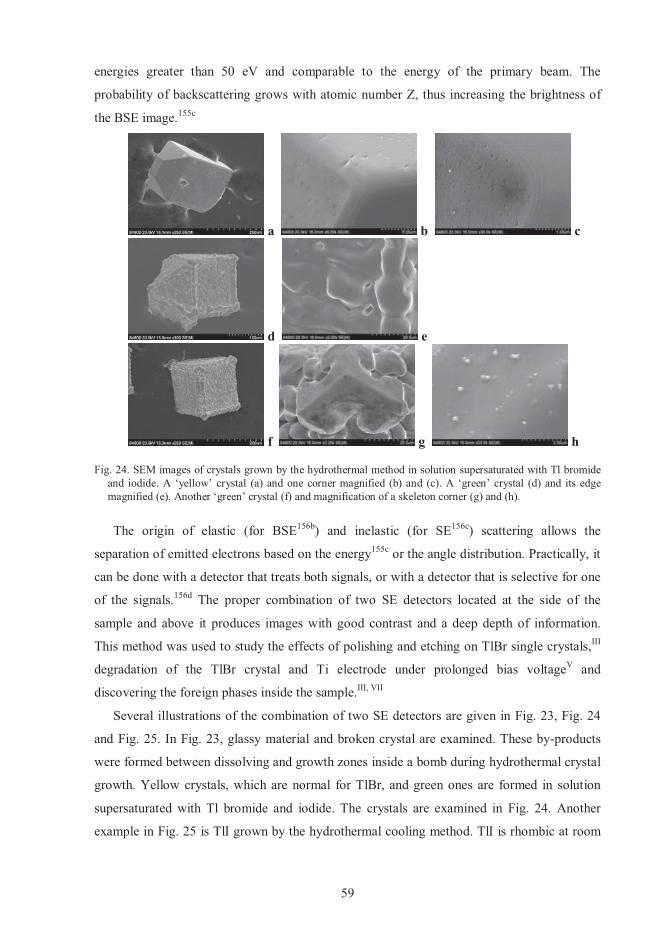
59
energies greater than 50 eV and comparable to the energy of the primary beam. The
probability of backscattering grows with atomic number Z, thus increasing the brightness of
the BSE image.155c
a b c
d e
f g h
Fig. 24. SEM images of crystals grown by the hydrothermal method in solution supersaturated with Tl bromide and iodide. A ‘yellow’ crystal (a) and one corner magnified (b) and (c). A ‘green’ crystal (d) and its edge magnified (e). Another ‘green’ crystal (f) and magnification of a skeleton corner (g) and (h).
The origin of elastic (for BSE156b) and inelastic (for SE156c) scattering allows the
separation of emitted electrons based on the energy155c or the angle distribution. Practically, it
can be done with a detector that treats both signals, or with a detector that is selective for one
of the signals.156d The proper combination of two SE detectors located at the side of the
sample and above it produces images with good contrast and a deep depth of information.
This method was used to study the effects of polishing and etching on TlBr single crystals,III
degradation of the TlBr crystal and Ti electrode under prolonged bias voltageV and
discovering the foreign phases inside the sample.III, VII
Several illustrations of the combination of two SE detectors are given in Fig. 23, Fig. 24
and Fig. 25. In Fig. 23, glassy material and broken crystal are examined. These by-products
were formed between dissolving and growth zones inside a bomb during hydrothermal crystal
growth. Yellow crystals, which are normal for TlBr, and green ones are formed in solution
supersaturated with Tl bromide and iodide. The crystals are examined in Fig. 24. Another
example in Fig. 25 is TlI grown by the hydrothermal cooling method. TlI is rhombic at room
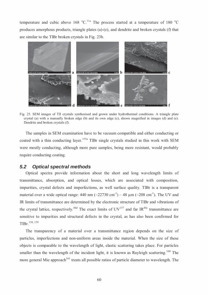
60
temperature and cubic above 168 oC.11a The process started at a temperature of 180 oC
produces amorphous products, triangle plates (a)-(e), and dendrite and broken crystals (f) that
are similar to the TlBr broken crystals in Fig. 23b.
a b c
d e f
Fig. 25. SEM images of TlI crystals synthesised and grown under hydrothermal conditions. A triangle plate crystal (a) with a manually broken edge (b) and its own edge (c), shown magnified in images (d) and (e). Dendrite and broken crystals (f).
The samples in SEM examination have to be vacuum compatible and either conducting or
coated with a thin conducting layer.155a TlBr single crystals studied in this work with SEM
were mostly conducting, although more pure samples, being more resistant, would probably
require conducting coating.
5.2 Optical spectral methods Optical spectra provide information about the short and long wavelength limits of
transmittance, absorption, and optical losses, which are associated with composition,
impurities, crystal defects and imperfections, as well surface quality. TlBr is a transparent
material over a wide optical range: 440 nm (~22730 cm-1) – 48 μm (~208 cm-1). The UV and
IR limits of transmittance are determined by the electronic structure of TlBr and vibrations of
the crystal lattice, respectively.44d The exact limits of UV157 and far IR44c transmittance are
sensitive to impurities and structural defects in the crystal, as has also been confirmed for
TlBr.158, 159
The transparency of a material over a transmittance region depends on the size of
particles, imperfections and non-uniform areas inside the material. When the size of these
objects is comparable to the wavelength of light, elastic scattering takes place. For particles
smaller than the wavelength of the incident light, it is known as Rayleigh scattering.160 The
more general Mie approach161 treats all possible ratios of particle diameter to wavelength. The

61
result of scattering is directly observed in a baseline of optical spectra as deviations from
100% of transmittance. Since polishing of the surface can be controlled to within several
nanometres, the effect of surface roughness is larger in UV-Vis than in IR spectra. This is
particularly valid for TlBr materials, whose softness does not permit to produce crystal faces
of high quality, and therefore, transmittance of TlBr samples in the visible region is
decreased. In Fig. 26, the effect of transmittance reduction is much greater for Vis than for IR
spectra. The transmittance UV-edges of the samples match each other, since the crystals have
been cut from the same part of an ingot. However, their base line levels vary considerably due
to low surface quality, as also indicated by the Vis-reflectance spectra.
Fig. 26. Transmittance (T, thick lines) and reflectance (R, thin lines) UV-Vis spectra (left) and IR transmittance base line (right) of TlBr crystalline samples of series Lis27.
In this thesis, the quality of the TlBr samples was examined by UV-Vis transmittance and
reflectance spectra recorded using a HITACHI U-2000 Spectrophotometer.VII Transmittance
and impurity control in the IR range was done by measuring spectra with a Perkin Elmer
Spectrum One spectrometer equipped with a Universal ATR Diamond/ZnSe unitI and Perkin
Elmer FT-IR system Spectrum GX.VII
5.2.1 FTIR spectra A second phenomenon affecting transparency is absorption due to impurities built into the
lattice. When the impurity is a molecule or anion, it has absorption bands that are specific to
that group, which can be easily determined by the IR spectroscopy.162 Transmittance spectra
are used for quantitative determination of relatively large amounts of impurities distributed
over the material bulk. The attenuated total reflectance (ATR) technique allows determination
of trace amounts of impurities. The physical basis of ATR leads to a limited penetration of the
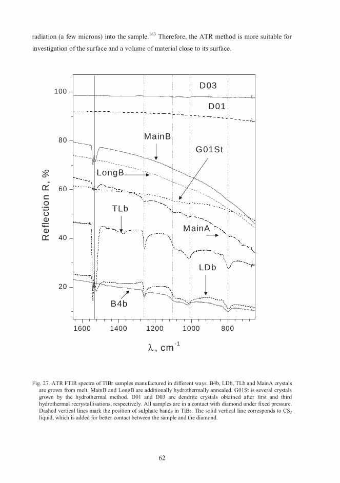
62
radiation (a few microns) into the sample.163 Therefore, the ATR method is more suitable for
investigation of the surface and a volume of material close to its surface.
Fig. 27. ATR FTIR spectra of TlBr samples manufactured in different ways. B4b, LDb, TLb and MainA crystals are grown from melt. MainB and LongB are additionally hydrothermally annealed. G01St is several crystals grown by the hydrothermal method. D01 and D03 are dendrite crystals obtained after first and third hydrothermal recrystallisations, respectively. All samples are in a contact with diamond under fixed pressure. Dashed vertical lines mark the position of sulphate bands in TlBr. The solid vertical line corresponds to CS2liquid, which is added for better contact between the sample and the diamond.
1600 1400 1200 1000 800
20
40
60
80
100
B4b
LDb
TLb
MainA
G01StMainB
LongB
D03
D01
Ref
lect
ion
R, %
� , cm-1
63
Interpolation of ATR results to the whole sample volume should take into account any
possible impurity depth profile near the surface, for example, due to aging.56 In Fig. 27, the
ATR FTIR method is used for qualitative characterisation of TlBr samples made by different
methods. The samples are dissimilar as shown by base level behaviour, as well as by sulphate
content. However, the origins of these differences, whether they be crystal growth, treatment
or aging, is not clear, because the method only characterises the material near its surface.
Due to impurities inside the lattice of a Tl halide, the experimental value of the coefficient
of bulk absorption (10-5 cm-1 at �=10,6 �m) is three order less than the theoretical value.53
The key impurities, which are introduced by the manufacturing processes, decomposition
reactions of by-product and ageing, are oxides of sulphur, carbon, nitrogen, chlorine and
hydrogen. Their typical IR frequencies are 1200 and 620 cm-1 (for SO4-2), 1400-1500 cm-1
(for CO3-2), 2100 cm-1 (for NCO-), 960 cm-1 (for ClO3
-), 1380 and 830 cm-1 (for NO3-), and
1600-1700 cm-1 and 3200-3600 cm-1 (for H2O).44c Sulphate,50, 164 nitrate54 and water53
impurities, and their derivatives are considered the most deleterious with respect to the
transparency of Tl halides and their aging. Due to the effects of the crystal field,162 the
absorption bands may split, or become hidden; lines active only in Raman spectroscopy often
become active in IR spectra, and vice versa. For example, the orientation effects of a nitrate
group inside the lattice can change the intensities and appearance of the bands in an IR-
spectrum after annealing.54 The absorption bands of water, as well as nitrate and sulphate
ions, in different solids are summarised in Table 5, Table 6, Table 7. Assignments used for the
bands are made according to Nakamoto.162
In general, water in lattices absorbs at 3550-3200 cm-1 (symmetric 1 anti-symmetric 3
OH stretching) and at 1630-1600 cm-1 (HOH bending 2).162b Additional bands at ~600 cm-1
and ~500 cm-1 observed in Tl halides are suggested to be caused by TlnOm impurities formed
by the reaction of water with the Tl halide.53
Table 5. Vibrational frequencies of water (C2v) in solid crystals.
Crystal 1 3 2 (?Tl2O) (?Tl4O2) Ref Solid 3400 3220 1620 162aTlCl 3345 1641 644 - 53Tl(Cl,Br) 3344 1644 645 507 53TlBr 3370 1630 604 469 53Tl(Br,I) 3380 1628 594 462 53
In sodium and potassium nitrates, the nitrate ion is planar.162c By analogy with the lattices
of NaCl and CsCl, in which the impurity NO31--ion has been studied, the impurity bands in
TlBr can be assigned. Additional bands at 1190 cm-1 and 824 cm-1 observed in TlBr are

64
suggested to be caused by either NO2-1 or by the formation of complexes that are more
complicated than the NO31--ion. The intensity of the 4 band is proposed to be small.54
Table 6. Vibrational frequencies of the nitrate ion (planar) in solid crystals. Frequencies 1 and 2 are Raman (R) and IR active, respectively.
Crystal IR/R 1(A1´) 2(A2´´) 3(E´) 4(E´) RefNa[NO3] IR 831 1405 692 162cNa[NO3] R 1068 1385 724 162cK[NO3] IR 828 1370 695 162cK[NO3] R 1049 1390 716 162cTlBr IR 835 1373 weak? 54
Impurities of sulphur and its compounds (S, S2-, SO32-, SO4
2-) are often found in optical
materials, since source materials and reagents used during the manufacturing process, as well
as air, contain them. The most probable form of sulphur in Tl halides is the sulphate ion.50
The free sulphate ion has the symmetry point group Td. Only 3 and 4 frequencies are IR-
active. However, a reduction of the symmetry, for example by coordination,162e inside the
lattice can cause the vibrations to degenerate and activate Raman modes in the infrared
spectrum. The appearance of additional lines and their splitting is explained by the formation
of pairs between sulphate ions and a metal, defect or impurity.164 The process may be
dynamic, since the number and intensity of the bands is not reproduced from sample to
sample with the same composition.50
Table 7. Vibrational frequencies of sulphate ion (tetrahedral) in solid crystals. Only frequencies �3 and �4 are IR active.
Crystal 1 2 3 4 Ref[SO4]2- 983 450 1105 611 162dTlCl-TlBr ~960, 997 1090, 1130 626 50*TlBr-TlI 997 1106, 1149, 1163 628 44c* TlBr 800 1010, 1100, 1260 Fig. 27
* - assignments were not made
5.3 X-ray diffraction methods (XRD) Material characterisation by the use of X-ray diffraction methods has been known since
the discovery of the wave character of X-ray radiation by Max von Laue in 1912.165 The
powder diffraction method was devised independently in 1916 by Debye and Scherrer and in
1917 by Hull.166 After Klug and Alexander,124 the powder diffraction method became a
routine technique for identification of compounds and impurities and their quantification.
Data collection has been considerably simplified by computer-based instruments, which are
supplied with software packages for rather tedious data reduction. Instrumentation and

65
experimental procedures have been widely developed for different forms of substances, i.e.
for single crystals,125 powders167, 165, 166 and thin films.168
In this work, a Philips powder diffractometer (PW1710/00) supplied with PC-APD
software (PW1877/42) was used for phase purity testing of TlBr,I the identification of
reaction by-products and localisation of impurities forming their own phases.IV, V A D8
Advanced Bruker X-ray diffractometer was used for the orientation of single crystals of TlBr
and their quality control by the rocking curve method.I-VII. For 2��� scans was used a
PANalytical X'Pert Pro MPD X-ray diffractometer.178
5.3.1 Penetration depthX-rays are absorbed in materials by photo-electric effect, and are scattered by elastic
Rayleigh and inelastic Compton mechanisms. As in optics, total attenuation follows the
Bouguer–Lambert–Beer law for a given wavelength �: I(d) = Io exp(-μ � d), where d is the
length of the path of the X-rays inside the material, � is its density and μ is the mass
attenuation coefficient. The coefficient μ can be computed from the composition of the
material: μ = � ci μi, where ci is the mass proportion of a chemical element i, and μi is its
attenuation coefficient.169
The significance of absorption coefficients to diffraction experiments is that only a part of
the material is represented in diffraction patterns. The thickness of the ‘work’ layer
(penetration depth) depends on the wavelength of the X-rays and the angle at which the
incident beam strikes the sample (�). Penetration depth Pd of TlBr in the range 20o - 70o of 2�
is 2.5 μm and 8.2 μm for reflections from (100)- and (300)-planes, respectively (Table 8).
Thus, as in the case of ATR FTIR, XRD methods can characterise a relatively thin layer of the
TlBr crystal, in which surface effects have a clear contribution.
Table 8. X-ray penetration depth Pd (μm) for 98% contribution to the diffracted beam (I(d) / Io) for TlBr, TlI and, for comparison, for Si and some metallic electrode materials. Cu-radiation (K1) at incident angle �.Calculations performed using the program Diffrac-plus, AbsorbDX V.1.1.4 (Bruker Advanced X-ray solutions).
�� Pd (TlBr) Pd (TlI) Pd (Si) Pd (Pd) Pd (Au) Pd (Ti) Pd (Al) 20 2.450 1.922 24.370 1.397 0.863 4.647 26.180 45 5.399 4.235 53.070 3.080 1.902 8.037 57.690 70 8.093 6.347 80.490 4.616 2.851 12.050 86.460 90 9.977 7.825 99.230 5.690 3.515 14.850 106.600 150 13.630 10.690 135.600 7.773 4.801 20.290 145.600 180 14.110 11.070 140.300 8.048 4.971 21.000 150.700
66
5.3.2 Data collection and specimen displacement The collection of the data with a counting detector, which sums the integer number of
counts per fixed time interval, follows the probability distribution p of the Poisson random
variable n: p(n, μ) = exp(-μ) μn / n!, where n (here) is number of counts and μ is the average
number of counts or a signal level. In a Poisson distribution, the statistical standard deviation
� is directly connected with the mean μ: �2 = μ.170 So, a relative error is about �/μ = μ-1/2.
Thus, in order to decrease the relative error by factor K, the signal level μ or time of the data
collection should be increased by factor K2. Although modern searching programs can find
peaks on a coarse background with criteria less than 1�, Poisson’s approach helps with
planning the data collection experiment in order to have reliable peaks.
For XRD data reduction the programs require precise values, for example, of peak
positions, with an error often less than a scanning step (0.02o of 2� in the indexing program
TREOR). Approximately half of the error in peak location is due to instrumental error.171 The
discrepancy in 2� peak position, the specimen-displacement error, is by far the largest of the
errors found in XRD powder data.167a Even in the case where the sample holder itself can be
accurately referenced to a machined surface on the goniometer, due to the different
attenuation coefficients of the sample and reference material it is difficult to set the sample
into the correct position. Since a Si-standard is commonly used for instrument alignment, for
TlBr samples this creates a problem, because the penetration depth for TlBr is ten times
smaller than for Si (Table 8).
The specimen-displacement error can be expressed as follows165a: �(2�) = 2 S cos(�) / R,
where S is the displacement of the specimen from the focusing circle with radius R. The error
can be eliminated by the use of an internal standard. A typical procedure includes the fitting
of peak positions of the standard, and then correction of the sample pattern using the S value
obtained.172 However, for a slice of a single crystal of TlBr, for which only one of a few
reflections can be registered, the only way to decrease the effect of the specimen-
displacement error is careful instrument alignment followed by variation of its Z (vertical) -
coordinate.
5.3.3 Full width at half medium FWHM The width of the peak characterises crystalline quality of the crystal. The origins of the
broadening of peaks are crystallite domains (whose size is designated �) and strain (�). The
first term is usually associated with variation in the domain sizes and their disorientation.
Lattice strain � represents variable displacements of atoms from their sites in the idealised

67
crystal structure caused by dislocations, vacancies, interstitials, foreign atoms and similar
defects. Strained crystals are often composed of elastically strained micro-domains separated
by plastically-deformed regions of high defect density.167b Two determination methods for the
line broadening � have been described: (1) � + b = B and (2) �2 + b2 = B2, where b is
instrument broadening and B is the width of the observed diffraction line at its half-intensity
maximum, also known as FWHM. The first definition (1) is often associated with size effects,
while the second is related to the strain.
The crystalline size broadening �� is expressed by the Scherrer equation: �� = K �/ (� cos
�), where K is the domain shape factor, � is the wavelength, � is the average crystallite size,
and � is the Bragg angle. The peak breadth �� due to stress is related to the residual strain � by
�� = 4� tg �.165b The strain � can also be expressed as mean lattice distortion �d/d, where d is
the lattice parameter.173 The difference in angular dependence of size and strain broadenings
is the basis for size-strain analysis, which assists in separation of �� and �� fractions in the
common broadening (B – b). For slices of TlBr single crystals, this analysis is difficult to
carry out since only one or a few reflection planes (for example, (110) and (220)) are detected
in a 2�-scan. Actually, disorientation between cut-off surface and reflection plane complicate
this problem. Therefore, in this work, crystal quality was mainly studied by the rocking curve
method.
5.3.4 Rocking curve method The broadening effects, both due to size and strain, generally produce a symmetric
broadening around the original peak position.165b This permits study of how perfect the stack
of hkl-planes of a given reflection over the sample is by scanning with the X-ray tube and
detector fixed relative to each other at the original 2�hkl angle (see Fig. 28). This is done for
every turn of the sample around the z-axis in the xy-plane. When, after a sequence of turns
around the z-axis, a scattering vector Shkl reaches the yz-plane, the intensity maximum of the
original peak will be recorded during the �-scan (Fig. 29A).
If the stack of planes is broken (domains) or/and bent (strains), the local disorientations of
planes of the stack will produce a splitting of the original peak and redistribution of its
intensity over the �-scan (Fig. 16 and Fig. 14B). Thus, step rotation over the z-axis and �-
scans result in the detection of several peaks, each having its the own - and �- orientation
with respect to the xyz-system. In fact, the -angle characterises the deviation of a reflection
plane from the slice’s surface during the cutting and polishing procedures. Both �- and -
angles characterise the disorientation between Shkl-vectors in 3D space. The rocking curve

68
method (�-scan) can be enhanced by variation of 2� that is the same as 2�-scans with series
of � fixed (see Fig. 29B).178 Thus, information about a domain size and strain in a crystal can
be extracted (compare chapter 5.3.3).
Fig. 28. Bruker setup for recording X-ray rocking curves, the xy-plane is fixed on a work table. The sample is positioned on an xy-flat surface of the diffractometer. A scattering vector S of a reflection hkl-plane forms a -angle to the z-axis and its S´-projection onto the xy-plane forms the �-angle to the x-axis. The X-ray source tube and detector fixed at 2�hkl are scanned over the angle � in the yz-plane (rocking curve �-scan).
TMZ21-Ing-An60
Sqr
t (C
ount
s)
0
100
1000
1e4
2000
3000
4000
5000
6000
2e4
3e4
Theta - Scale
8.7
8.8
8.9
9.0
9.1
9.2
9.3
9.4
9.5
9.6
9.7
9.8
9.9
10.0
10.1
10.2
10.3
10.4
10.5
10.6
10.7
10.8
10.9
11.0
11.1
11.2
11.3
11.4
11.5
11.6
11.7
11.8
11.9
12.0
12.1
12.2
12.3
12.4
12.5
12.6
12.7
12.8
12.9
13.0
13.1
13.2
13.3
13.4
13.5
13.6
13.7
13.8
13.9
14.0
14.1
14.2
14.3
14.4
14.5
14.6
14.7
14.8
Theta - Scale8.7 9 10 11 12 13 14
th=11.700 °
A B
Fig. 29. An X-ray study of a crystal grown by the TMZ method.178 (A) A rocking curve of the ingot’s area, which is free of strains [FWHM(�) = 0.1]. (B) 2��� scans of the slice N11 that was polished, etched and annealed [FWHM(�) = ~ (0.2+0.3)].
The X-ray rocking curve method has several limitations. The first is related to the
penetration depth, which is shown for several substances in Table 8. Secondly, the irradiated
area of the sample varies with �-scan as w/sin(�), where w is the beam thickness. Thirdly, an
�-scan is limited by geometry to angles of 0o to 2�o (see Fig. 28), and the diffractometer
construction often decreases additionally these limits.
x
y
zShkl
S´
2hkl
x-ray source detector
69
5.4 Electrical characterisation For improving the performance of the TlBr detector, preliminary electrical
characterisations of TlBr crystals are carried out in order to establish electrical parameters
(resistivity, capacitance, leakage current and temperature limits) for future use of the crystals
as detectors. There are two factors to be taken into account. The first one is quality of the
surface and electrodes, since they serve as the current supply, signal collectors and radiation
window. The interactions between the TlBr surface and metallic electrode are considered in
chapter 4, and the effects of metallisationIV and degradationV on TlBr single crystals have also
been studied. The second factor is related to the TlBr crystal electrode system, which is a
capacitor and therefore a time delay is used during the voltage sweeping.
For the electrical characterisation a Keithley 2400 Series Sourcemeter I-V and Agilent/HP
4155A semiconductor parameter analyzerVII were used. Frequency dependence of capacitance
and C–V curves were measured with a Precision LCR Meter HP4284A (Hewlett Packard).III, V
Beckman (Modell 2400) or Perkin Elmer MPF-44A spectrophotometers were used for
obtaining a photo-response from crystals.II, III, V The X-ray response of the TlBr crystals was
studied using Cu-radiation from a Philips X-ray diffractometer, PW1710/00.II, IV MULTI-
POWER/SPECTRUM (Bruker Baltic)147 was used for characterisation of the TlBr crystals as
detectors.VI, VII
5.5 Elemental analysis An inductively Coupled Plasma Mass Spectrometry (HR-ICPMS ELEMENT, Finnigan
MAT, Bremen/Germany, equipped with a microconcentric nebulizer MCN-100, CETAC
Tech., Omaha/USA) was used for the trace element analysis. The method permitted
simultaneous determination of Al, As, Bi, Ca, Co, Cr, Cu, Fe, Mg, Na, Nb, Ni, P, Pb, Pd, Pt,
S, Sb, Si, V and Zn in crystals of TlBr and its solutions.I The analysis was done by totally
dissolving the samples. The sample preparation steps and subsequent measurements were
performed under clean room conditions. The detection limits were between 0.001 and
0.01ng/ml, depending on the element, with a dynamic range of more than eight orders of
magnitude. The details of trace element analysis with ICPMS have been described in Ref.174
The elemental composition was also studied by energy-dispersive X-ray spectroscopy
(EDS) analysis using an Oxford INCA350 EDS connected to a Hitachi S-4800 FESEM.III, V,
VII The instrument is supplied with software for spectrum collection, peak identification and
quantitative analysis. The instrument allows point analysis, line scanning and elemental
mapping of the image obtained by SEM. Since chemical analysis is performed by measuring
70
the energy and intensity distribution of the x-ray signal generated by a focused electron beam,
the depth depends on the energy and incident angle of the beam, properties the material being
examined and energy of the X-ray radiation (see Table 8). The minimum size for point
analysis is associated with a minimum probe current. For example, a 20-nm probe diameter
has been estimated for conventional 20 kV voltage and a minimum 10 pA probe current.156f,
The EDS system coupled with SEM was used in this work to provide information concerning
non-uniformity of the sample on the elemental scale.III, V, VII
Conclusion In the field of gamma-ray detection there is a great need for high performance detectors
that work at ambient conditions. The applications that need these detectors range from
medical and military to astrophysical. A single crystal of TlBr is a promising candidate for
gamma-ray detection at room temperature because of its high stopping power, density and
wide bandgap (chapter 2). However, this material has less developed technology for crystal
growth and purification than, say, that for Si and Ge detectors. As a result, purity and crystal
quality are the main problems of TlBr crystals as detectors.I, II Therefore, the technological
processes for TlBr detector manufacturing were studied with respect to obtaining the best
purity for TlBr and the highest quality of TlBr crystals.
The improvement of purity and crystal quality was the central topic in published papersI-
VII and in chapters 3 and 4. In chapter 3.1, wet and dry methods of synthesis of TlBr, as raw
material, were studied and compared. Precursors were shown to have the drastic effects on
quality of material and its aging. The hydrothermal method for TlBr synthesis was proposed
for better purityI. Purification methods by recrystallisation from vapour, molten state and
water solutionsI were considered in chapter 3.2. A combination of wet (hydrothermal) and dry
(Bridgman and TMZ) methods of purification was shown to be successful for obtaining high
quality crystals.77, VI
Various methods for crystal growth were summarised in chapter 3.3. Crystals grown from
water solutions by the hydrothermal method were small, but available for production of the
counting gamma-ray detectors. The crystal growth from melts currently is the only method by
which large ingots of Tl halides can be produced. Bridgman and TMZ methods were studied
and used for growth of large crystals of TlBr. Basically, non-uniformity of TlBr crystals
grown from melt was shown to stem from the walls of the crucible. In Bridgman method,
recent attempts to decrease the adhesion by increasing the temperature of melt deteriorated
also the purity of a crystal by dissolving the crucible components.VII Thus, the problem of
71
interaction of an ingot and crucible material persists. In the horizontal TMZ method, crystals
grown were less stressed than in the Bridgman method possibly due to releasing tension from
the walls through the top surface which was open.178 Crystal quality can be improved by
annealingI, II (chapter 3.4). Various annealing processes were used in this work to decrease the
strains and number of boundaries in the crystal and make it more uniform and pure. The
annealing improved electrical characteristics as well.II
During TlBr detector fabrication (chapter 4) cutting and polishing the crystals were
showed to make pronounced and deep structural surface damage.III Chemical polishing and
etching were used and chemical cutting was proposed in order to avoid mechanically
damaging the material and to clean its surface. Metallisation effects were demonstrated to
depend on the metal and deposition conditions.IV The stability of TlBr-metal interfaces was
influenced to much extent by an ionic current, which produced degradation of the TlBr crystal
and metallic electrodes.V The use of the purest TlBr of highest crystal quality and lowering of
the temperature of the device below the level of noticeable ionic current seems to be the only
solution for suppressing the polarisation effects associated with an ionic current and making
the gamma-ray detector more durable.
In this thesis, the technological stages, such as preparation of TlBr raw material, crystal
growth, annealing and detector fabrication, were optimised using various instrumental
characterisation methods (chapter 5). Different technological processes were studied by
elemental analysis of corresponding samples using HR-ICPMS.I The FTIR method was
reviewed and used to determine the impurity molecules or anions that were built into the
lattice. The ATR-FTIR technique was applied for qualitative characterisation of raw material
and single crystals of TlBr.I Also, FTIR base lines were used for the characterisation of
quality of the samples.VII, 178 A polarisation microscope was used to determine the extent of
non-uniformity in crystals.II-IV, VI, VII The study of the surface morphology was carried out with
SEM, and the elemental composition of irregularities observed was studied using an EDS
system.III, V, VII The phase purity characterisation of TlBr was done using X-ray powder
diffraction.I, IV The effects of technological operations on the quality of single crystals were
studied by the X-ray rocking curve method.I-VII Characterisation of electrical properties of
TlBr single crystals was carried out by measuring I-V curves, photocurrent, current-time
(electro-aging) and capacitance characteristics.I-V, VII Final qualitative characterisation of a
crystal as a detector was done using gamma ray spectroscopy methods.77, VI, VII
The central concept for this thesis was to recrystallise TlBr from water solution in a chain
of routine purification methods. This significantly improved the detector performance. A
72
second approach was the use of annealing methods for improving the crystal quality and
purity. The innovation in this thesis was the use of the hydrothermal method for the synthesis,
purification, annealing and crystal growth of TlBr. These techniques allowed detector-grade
TlBr single crystals to be produced.77, VI The best crystal had parameters, the mobility-lifetime
product for electrons of 3.3x10⁻⁴ cm2/V and resistivity of 2.9x10¹²�� cm (at -20 oC), which
were approached using only hydrothermal recrystallisation and seven TMZ passes.
Looking ahead, the crystal growth, annealing and TlBr detector fabrication techniques
could be developed for making non-strained and pure crystals of TlBr. Future steps should
solve the existing problems such as adhesion to crucible material, strain-less treatment of
samples, and develop new technological stages, for example to use the electrochemical
methods for purification. The study of non-stoichiometry in TlBr and its doping will allow to
make p- and n-type materials that could be used in a creation of diode structures, and thus, to
decrease the leakage current in TlBr detectors. The other problem is an ionic current and its
interaction with electrode material. The formation of barriers to the ionic current and
electrochemical reaction on the electrode could make the TlBr detector more durable.

73
ReferencesRef.
Num. Publication
1 R. Hofstadter, Thallium Halide Crystal Counter, Phys. Rev. 72(11) (1947) 1120. 2 A. Owens, A. Peacock, Compound semiconductor radiation detectors, Nucl.
Instr. and Meth. A 531 (2004) 18. 3 R. Hofstadter, Crystal counters - II, Nucleonics 4(5) (1949) 29. 4 F. Olschner, M. Toledo-Quinones, K. S. Shah, J. C. Lund, Charge carrier
transport properties in thallium bromide crystals used as radiation detectors, IEEE Trans. Nucl. Sci. 37(3) (1990) 1162.
5 K. S. Shah, F. Olschner, L. P. Moy, J. C. Lund, M. R. Squillante, Chracterization of thallium bromide nuclear detectors, Nucl. Instr. and Meth. A 299 (1990) 57.
6 F. Olschner, K. S. Shah, J. C. Lund, J. Zhang, K. Daley, S. Medrick, M. R. Squillante, Thallium bromide semiconductor X-ray and gamma-ray detectors, Nucl. Instr. and Meth. A 322 (1992) 504.
7 P. J. Durrant, B. Durrant, Introduction to advanced Inorganic chemistry, Longmans, (1962): a - p. 487; b - p. 557; c - p. 558; d - p. 561.
8 F. A. Cotton, G. Wilkinson, C. A. Murillo, M. Bochmann, Advanced inorganic chemistry, 6th ed., John Wiley & Sons, Inc., (1999), p. 175; b - p. 204 and ibid.
9 N. V. Sidgwick, Variable valence, Inst. intern. chimic Solvay (1928). 10 A. J. Downs (ed.), Chemistry of Aluminium, Gallium, Indium and Thallium,
Blackie Academic & Professional, London, 1993: a - pp. 11-12, 39-46, 111-118. 11 H. Remy, Treatise on Inorganic Chemistry, v. 1, Elsevier Publishing Company
(1956): a - p. 381 and ibid.; b - p. 385 and ibid. 12 W. C. Price, W. F. Sherman and G. R. Wilkinson, Infra-red studies on
polyatomic ions isolated in alkali-halide lattices, Spectrochimica Acta, 16 (1960) 663.
13 John Courtney Decius and Robert Maurice Hexter, Molecular Vibrations in Crystals, McGRAW-HILL INTERNATIONAL BOOK COMPANY, New York, 1977: a – p. 289 and ibid.
14 Alan F. Clifford, Inorganic Chemistry of Qualitative Analysis, Prentice-Hall, Inc., Englewood Cliffs, N. J., 1961, p. 81 and ibid.
15 F. A. Cotton and G. Wilkinson, , Advanced inorganic chemistry (a comprehensive text), Advanced inorganic chemistry, 2nd ed., Interscience Publishers, John Wiley & Sons, New York, London, Sydney, 1968: a - p. 453; b - p. 467; c - p. 495.
16 Per Kofstad, Nonstoichiometry, diffusion and electrical conductivity in binary metal oxides, New York : Wiley, 1972
17 W. Lehfeldt, Electric conductivity of single crystals, Z. Physik 85 (1933) 717. 18 W. Lehfeldt, Electron conduction in crystals of silver and thallium halides,
Nachr. Ges. Wiss. Gottingen Math. physik. Klasse, Fachgruppe II (1935), 1 1711.
19 P. J. Van Heerden, The crystal counter, Dissertation, Utrecht University, 1945. 20 R. Hofstadter, Crystal counters - I, Nucleonics 4(4) (1949) 2. 21 J. Bardeen and W. H. Brattain, The Transistor, A Semi-Conductor Triode, Phys.
Rev. 74(2) (1948) 230. 22 W. H. Brattain and J. Bardeen, Nature of the forward current in germanium point
contacts, Phys. Rev. 74(2) (1948) 231.
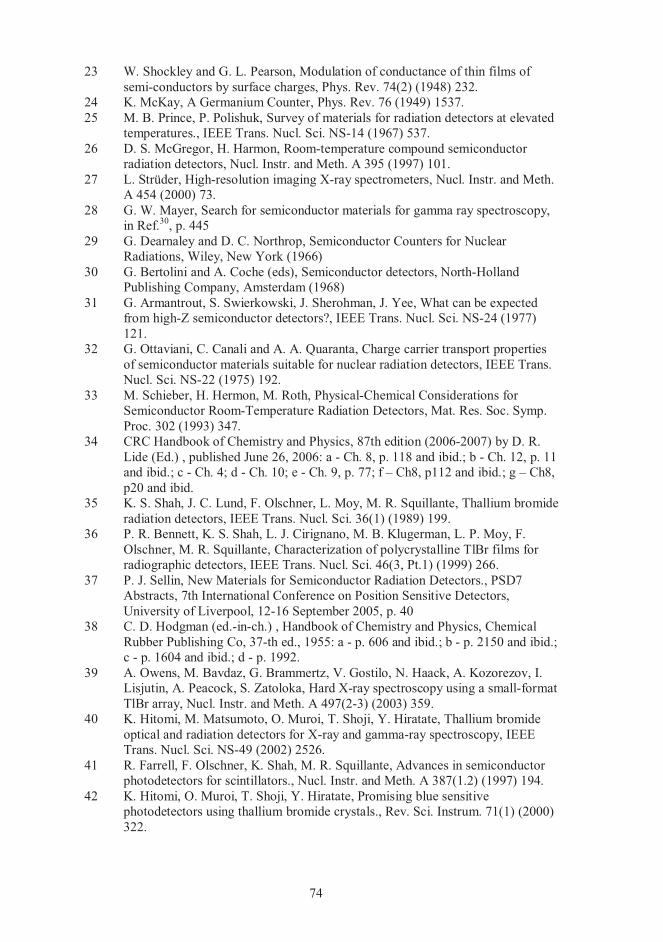
74
23 W. Shockley and G. L. Pearson, Modulation of conductance of thin films of semi-conductors by surface charges, Phys. Rev. 74(2) (1948) 232.
24 K. McKay, A Germanium Counter, Phys. Rev. 76 (1949) 1537. 25 M. B. Prince, P. Polishuk, Survey of materials for radiation detectors at elevated
temperatures., IEEE Trans. Nucl. Sci. NS-14 (1967) 537. 26 D. S. McGregor, H. Harmon, Room-temperature compound semiconductor
radiation detectors, Nucl. Instr. and Meth. A 395 (1997) 101. 27 L. Strüder, High-resolution imaging X-ray spectrometers, Nucl. Instr. and Meth.
A 454 (2000) 73. 28 G. W. Mayer, Search for semiconductor materials for gamma ray spectroscopy,
in Ref.30, p. 445 29 G. Dearnaley and D. C. Northrop, Semiconductor Counters for Nuclear
Radiations, Wiley, New York (1966) 30 G. Bertolini and A. Coche (eds), Semiconductor detectors, North-Holland
Publishing Company, Amsterdam (1968) 31 G. Armantrout, S. Swierkowski, J. Sherohman, J. Yee, What can be expected
from high-Z semiconductor detectors?, IEEE Trans. Nucl. Sci. NS-24 (1977) 121.
32 G. Ottaviani, C. Canali and A. A. Quaranta, Charge carrier transport properties of semiconductor materials suitable for nuclear radiation detectors, IEEE Trans. Nucl. Sci. NS-22 (1975) 192.
33 M. Schieber, H. Hermon, M. Roth, Physical-Chemical Considerations for Semiconductor Room-Temperature Radiation Detectors, Mat. Res. Soc. Symp. Proc. 302 (1993) 347.
34 CRC Handbook of Chemistry and Physics, 87th edition (2006-2007) by D. R. Lide (Ed.) , published June 26, 2006: a - Ch. 8, p. 118 and ibid.; b - Ch. 12, p. 11 and ibid.; c - Ch. 4; d - Ch. 10; e - Ch. 9, p. 77; f – Ch8, p112 and ibid.; g – Ch8, p20 and ibid.
35 K. S. Shah, J. C. Lund, F. Olschner, L. Moy, M. R. Squillante, Thallium bromide radiation detectors, IEEE Trans. Nucl. Sci. 36(1) (1989) 199.
36 P. R. Bennett, K. S. Shah, L. J. Cirignano, M. B. Klugerman, L. P. Moy, F. Olschner, M. R. Squillante, Characterization of polycrystalline TlBr films for radiographic detectors, IEEE Trans. Nucl. Sci. 46(3, Pt.1) (1999) 266.
37 P. J. Sellin, New Materials for Semiconductor Radiation Detectors., PSD7 Abstracts, 7th International Conference on Position Sensitive Detectors, University of Liverpool, 12-16 September 2005, p. 40
38 C. D. Hodgman (ed.-in-ch.) , Handbook of Chemistry and Physics, Chemical Rubber Publishing Co, 37-th ed., 1955: a - p. 606 and ibid.; b - p. 2150 and ibid.; c - p. 1604 and ibid.; d - p. 1992.
39 A. Owens, M. Bavdaz, G. Brammertz, V. Gostilo, N. Haack, A. Kozorezov, I. Lisjutin, A. Peacock, S. Zatoloka, Hard X-ray spectroscopy using a small-format TlBr array, Nucl. Instr. and Meth. A 497(2-3) (2003) 359.
40 K. Hitomi, M. Matsumoto, O. Muroi, T. Shoji, Y. Hiratate, Thallium bromide optical and radiation detectors for X-ray and gamma-ray spectroscopy, IEEE Trans. Nucl. Sci. NS-49 (2002) 2526.
41 R. Farrell, F. Olschner, K. Shah, M. R. Squillante, Advances in semiconductor photodetectors for scintillators., Nucl. Instr. and Meth. A 387(1.2) (1997) 194.
42 K. Hitomi, O. Muroi, T. Shoji, Y. Hiratate, Promising blue sensitive photodetectors using thallium bromide crystals., Rev. Sci. Instrum. 71(1) (2000) 322.

75
43 K. Hitomi, O. Muroi, T. Shoji, Y. Hiratate, H. Ishibashi, M. Ishii, Thallium bromide photodetectors for scintillation detection., Nucl. Instr. and Meth. A 448(3) (2000) 571.
44 S. V. Bogdanov (ed.), Crystals of Thallium Halides (Production, properties and application), "Nauka", Sibirskoe otdelenie, Novosibrsk, 1989: a - p. 20; b - p. 29 and ibid.; c - p. 31 and ibid.; d - p. 45 and ibid.; e - p. 8; f - p. 19; g - p. 66.
45 D. A. Pinnow, A. L. Gentile, A. G. Standlee, A. J. Timper, L. M. Hobrock, Polycrystalline fiber optical waveguides for infrared transmission, Appl. Phys. Lett. 33(1) (1978) 28.
46 J. A. Harrington, A. G. Standlee, Attenuation at 10.6 um in loaded and unloaded polycrystalline KRS-5 fibers, Appl. Opt. 22(19) (1983) 3073.
47 A. L. Gentile, Infrared Fiber Optical Materials, in Fiber Optics: Advances in Research and Development, B. Bendow and S. S. Mitra, Eds (Plenum, New York, 1979) 105.
48 M. E. Lines, Scattering losses in optic fiber materials, I. A new parametrization, J. Appl. Phys. 55(11), 1 June (1984) 4052.
49 M. E. Lines, Scattering losses in optic fiber materials, II. Numerical estimates, J. Appl. Phys. 55(11), 1 June (1984) 4058.
50 I. S. Lisitskii, V. F. Golovanov, V. G. Plotnichenko, Effect of oxygen-containing anion impurities on spectral transparency of thallium halogenide crystals, Part III. sulfate ions, Tsvetnye Metally 11 (2001) 73.
51 M. S. Kouznetsov, I. S. Lisitsky, S. I. Zatoloka, V. V. Gostilo, Development of the technology for growing TlBr detector crystals, Nucl. Instr. and Meth. A 531 (2004) 174.
52 K. A. Bolshakov (ed.), Chemistry and technology of rare and scattered elements, 2-nd ed., Visshaja Shkola, Moskva, 1 (1976): a - p. 359 and ibid.; b - p. 332.
53 I. S. Lisitskii, V. F. Golovanov, A. B. Chapyzhnikov, V. G. Plotnichenko, Effect of oxygen-containing anionic impurities on spectral clarity of thallium halogenide crystals, Part I. Water molecules, Tsvetnye Metally 8 (2001) 79.
54 I. S. Lisitskii, V. F. Golovanov, V. G. Plotnichenko, A. B. Chapyzhnikov, The effect of oxygen-containing anionic impurities on spectral clarity of thallium halogenide crystals, Part II. Nitrate ions, Tsvetnye Metally 9-10 (2001) 66.
55 J. A. Wysocki, R. N Schwartz, A. G. Standlee, R. G. Wilson, A. R. Williams, Aging effects in extruded polycrystalline thallium bromo-iodide fibers, Proc. SPIE-Int. Soc. Opt. Eng. 843 (1988) 94.
56 J. A. Wysocki, R. G. Wilson, A. G. Standlee, A. C. Pastor, R. N. Schwartz, A. R. Williams , G.-D. Lei, L. Kevan, Aging effects in bulk and fiber TlBr-TlI, J. Appl. Phys. 63(9) (1988) 4365.
57 HSC Chemistry 5.1 for Windows, Chemical Reaction and Equilibrium Software with Extensive Thermochemical Database, ver. 5.1 , Outokumpu Research Oy.
58 D. R. Lide (ed.-in-ch.) , CRC Handbook of Chemistry and Physics, CRC Press, 82-nd ed. (2001-2002): a - Ch12-p. 228 and ibid.; b - Ch12-p. 1; c - Ch.8 p.21 and ibid.
59 G. MULLER und G. GNAUCK, Reinste Gase, VEB Deutscher Verlag der Wissenschaften, Berlin 1965 (in German).
60 U. G. Frolov, Course of the colloid chemistry, Kemia, Moskva, 1982, p. 270 and ibid. (in Russian).
61 G. Brauer, Handbuch der Präparativen Anorganischen Chemie, Ferdinand Enke Verlag Stuttgart (1954), p. 654 and ibid.

76
62 J. Waser, Basic Chemical Thermodynamics, W.A. Benjamin, Inc., New York (1966), p. 145 and ibid.
63 H. Kanzaki, K. Kido, Purification of Alkali Halide Crystals through Fractional Distillation and Normal Freezing, J. Phys. Soc. Japan 15 (1960) 529.
64 R. McFee, Foreign Ion Rejection in the Growth of Sodium Chloride Single Crystals from the Melt, J. Chem. Phys. 15 (1947) 856.
65 O. L. Kreinin and K. M. Rozin, Distribution coefficients of divalent impurities in alkali halide crystals, Crystallography 18(2) (1973) 432 (in Russian).
66 I. B. Oliveira, F. E. Costa, J. F. D. Chubaci, M. M. Hamada, Purification and preparation of TlBr crystals for room temperature radiation detector applications, IEEE Trans. Nucl. Sci. 51(3, Pt. 3) (2004) 1224.
67 C. H. Mesquita, I. B. Oliveira, J. F. D. Chubaci, M. M. Hamada, Multielementar segregation coefficient of thallium bromide impurities from inductively coupled plasma mass spectroscopy measurements, (un-published).
68 W. Pfann, Zone melting, John Wiley, New York (1966): a - p. 18; b - p. 100; c - p. 48.
69 W. A. Tiller, K. A. Jackson, J. W. Rutter, B. Chalmers, The Redistribution of Solute Atoms during the Solidification of Metals, Acta Met. 1 (1953) 428.
70 W. G. Pfann, Comment on paper by Tiller, Jackson, Rutter and Chalmers, Acta Met. 1 (1953) 763.
71 J. A. Burton, R. C. Prim, W. P. Slichter, The Distribution of Solute in Crystals Grown from the Melt. Part I. Theoretical, J. Chem. Phys. 21 (1953) 1987.
72 J. A. Burton, E. D. Kolb, W. P. Slichter, J. D. Struthers, Distribution of Solute in Crystals Grown from the Melt. Part II. Experimental, J. Chem. Phys. 21 (1953) 1991.
73 B. L. Karger, L. R. Snyder, C. Horvath, An Introduction to Separation Science, A Wiley-Interscience publication, John Wiley & Sons, Inc. (1973), p. 312.
74 C. Berry, W. West, F. Moser, Silver Halides, in Ref. [78] p. 214; a - p. 227. 75 K. Hitomi, O. Muroi, T. Shoji, T. Suehiro, Y. Hiratate, Room temperature x- and
gamma-ray detectors using thallium bromide crystals., Nucl. Instr. and Meth. A 436(1.2) (1999) 160.
76 H. Kitaguchi, K. Amemiya, K. Yokoi, Y. Ueno, K. Tsuchiya, N. Yanagita, S. Kojima, K. Hitomi, T. Shoji, Semiconductor Radiation Detector and Radiation Detection Apparatus, US Pat. Appl. 2006/0065847 A1.
77 V. Kozlov, H. Andersson, M. Leskelä, H. Sipilä, Improved Process for the Detector Grade TlBr Single Crystals, 2006 IEEE Room-Temperature Semiconductor Detector (RTSD) Workshop, October 30 - November 3, San Diego, CA, US, R06-27.
78 J. J. Gilman (ed.), The Art and Science of Growing Crystals, John Wiley & Sons, Inc. (1963).
79 I. Tarján and M. Mátrai (eds.), Laboratory manual on crystal growth, Akadémiai Kiadó, Budapest (1972).
80 K. Nassau, Crystal growth techniques (in Technique of inorganic chemistry), John Wiley & Sons, Inc. (1968).
81 H. E. Buckley, Crystal Growth, John Wiley & Sons, Inc., New York, Chapman & Hall, Ltd., London (1951), p310 and ibid.
82 J. C. Brice, The growth of crystals from liquids, Amsterdam : North-Holland (1973).
83 J. C. Brice, The growth of crystals from the melt, Amsterdam : North-Holland (1965).
77
84 D. Elwell, H. J. Scheel, Crystal Growth from High-Temperature Solutions, Academic Press, London, New York, San Francisco (1975).
85 H. K. Henisch, Crystal Growth in Gels, The Pennsylvania State University Press.86 J. C. Brice, Crystal Growth, Ullman's Encyclopedia of Industrial Chemistry, 5-th
Ed, VCH A8, p. 99. 87 H. J. Scheel, T. Fukuda, Crystal Growth Technology, John Wiley & Sons Ltd
(2003): a - p. 16 and ibid.; b - p. 511 and ibid.; c - p. 548 and ibid. 88 H. Krebs, Grundzüge der Anorganischen Kristallchemie, Ferdinand Enke Verlag
Stuttgart, 1968. 89 A. K. Shukla, S. Radmas and C. N. R. Rao, Formation energies of Schottky and
Frenkel defects in thallium halides, J. Phys. Chem. Solids, 34(4) (1973) 761. 90 K. Hitomi, O. Muroi, M. Matsumoto, T. Shoji, Y. Hiratate, Large-volume
thallium bromide detectors for gamma-ray spectroscopy, IEEE Trans. Nucl. Sci. NS-48 (2001) 2313
91 N. Cabrera and R. V. Coleman, Theory of Crystal Growth from the Vapor, in Ref. [78] p. 3.
92 S. Kondo, T. Iton, T. Saito, M. Mekata, Well Defined Amorphous to Crystalline Transformation of Cold Condensed TlCl Films, Solid State Communications, 78(6) (1991) 557.
93 S. Kondo and M. Nakano, Optical Absorption near the Fundamental Edge in Amorphous Thallous Halides, J. Phys. Soc. Japan, 61(11) (1992) 4255.
94 S. Kondo, N. Yamagishi, T. Saito, Effects of Chemical Disorder on Crystallization Behavior in Amorphous TlCl1-xBrx Films Studied by UV Absorption Measurements, J. Phys. Soc. Japan, 67(1) (1998) 353.
95 S. Kondo, H. Tanaka, T. Saito, A simple method for preparing uniform amorphous films of mixed metal halides by means of two-source evaporation., Journal of Physics D: Applied Physics 33(22) (2000) 2973.
96 E. A. Secco, Heats of solution of TlI in TlNO3 and TlBr in TlI crystals. Phase diagrams of TlNO3-TlI and TlBr-TlI systems., Solid State Communications 115(8) (2000) 397.
97 R. R. Adzic, J. X. Wang, Bromide Adsorption Induced Formation of Thallium Bromide Adlayers with Varying Composition and Structure on the Au(111) Electrode Surface., J. Phys. Chem. B 102(33) (1998) 6305.
98 R. R. Adzic, J. X. Wang, Structure of Active Phases during the Course of Electrocatalytic Reactions, Journal of Physical Chemistry B 104(5) (2000) 869.
99 R. R. Adzic, J. X. Wang, Structures of surface adlayers and oxygen reduction kinetics., Solid State Ionics 150 (2002) 105.
100 A. Seidell (ed.) , Solubilities of inorganic and metal-organic compounds, 3-rd ed., D. Van Nostrand company, Inc. Vol.1 (1940) 1538, p. 1538.
101 S. Kondo, T. Iton, T. Saito, M. Mekata, Amorphous to Crystalline Transformation of Cold Condensed TlBr Films, J. Phys. Soc. Japan, 60(8) (1991) 2764.
102 M. Takano, Y. Takeda, O. Ohtaka, High pressure synthesis of solids, Encyclopedia of Inorganic Chemistry, p. 1372.
103 G. W. Morey, P. Niggli, The hydrothermal formation of silicates, J. Am. Chem. Soc. 35 (1913) 1086.
104 G. C. Kennedy, Pressure-Volume-Temperature relations in water at elevated temperatures and pressures, Am. J. Sci. 248 (1950) 540.
105 W. T. Read, Dislocations in Crystals, McGraw-Hill Book Company, Inc., 1953.

78
106 A. H. Cottrell, Dislocations and Plastic Flow in Crystals, in The International Series of Monographs on Physics, Oxford, at the Clarendon Press, 1958, p. 180 and ibid.
107 Recovery of metals, article in, Dictionary of Physical Encyclopaedia, v. 3, Soviet Encyclopedia, Moscow, 1963 (in Russian).
108 P. I. Poluhin, G. Ja. Gun, A. M. Galkin, Resistance of metals and alloys to plastic deformation (handbook), 2nd ed., Moskva, Metallurgija, 1983, p. 9 (in Russian)
109 M. Blackman and I. H. Khan, The polymorphism of thallium and other halides at low temperatures, Proc. Phys. Soc., London PPSOA, 77 (1961) 471.
110 J. Vaitkus, V. Gostilo, R. Jasinskaite, A. Mekys, A. Owens, S. Zatoloka, A. Zindulis, Investigation of degradation of electrical and photoelectrical properties in TlBr crystals, Nucl. Instr. and Meth. A 531 (2004) 192.
111 J. Vaitkus, J. Banys, V. Gostilo, S. Zatoloka, A. Mekys, J. Storasta, A. Zindulis, Influence of electronic and ionic processes on electrical properties of TlBr crystals., Nucl. Instr. and Meth. A 546(1-2) (2005) 188.
112 G. A. Samara, Pressure and temperature dependences of the ionic conductivities of the thallous halides TlCl, TlBr and TlI, Phys. Rev. B 23(2) (1981) 575.
113 N. H. Hartshorne, A. Stuart, Crystals and the Polarising Microscope , Edward Arnold (Publishers) Ltd., London 4-th ed. (1970): a - p. 19; b - p. 138; c - p. 101.
114 M. El Azab, C. R. McLaughlin, C. H. Champness, Preparation and characterization of tellurium surfaces, J. Crystal Growth, 28 (1975) 1.
115 I. B. Oliveira, F. E. Costa, P. K. Kiyohara, M. M. Hamada, Influence of crystalline surface quality on TlBr radiation detector performance, IEEE Trans. Nucl. Sci. (2005), 52(5, Pt. 3), 2058.
116 S. A. Varchenya, A. A. Simanovsky, S. V. Stolyarova, G. P. Upit, Adhesion phenomena on metal film /halide crystal (juvenile contact), I. Adhesion strength and intermolecular interaction, Latv. PSR Zinat. Akad., Fiz. Inst., Preprint LAFI-067, Salaspils (1984) 1-38 (in Russian): a - p. 11 and ibid.; b - p. 30.
117 K. Hitomi, M. Matsumoto, O. Muroi, T. Shoji, Y. Hiratate, Characterization of thallium bromide crystals for radiation detector applications., Journal of Crystal Growth 225(2-4) (2001) 129.
118 V. Gostilo, D. Gryaznov, I. Lisjutin, Technological limitations and processing-generated defects at the development of pixel and strip arrays, Nucl. Instr. and Meth. A 487(1-2) (2002) 13.
119 K. Hitomi, T. Murayama, T. Shoji, T. Suehiro, Y. Hiratate, Improved spectrometric characteristics of thallium bromide nuclear radiation detectors., Nucl. Instr. and Meth. A 428(2.3) (1999) 372.
120 G. V. Bunton, S. Weintroub, Chemical and thermal etching of antimony, J. Crystal Growth 2(2) (1968) 91.
121 S. Ahmed, S. Weintroub, The chemical and thermal etching of tellurium single crystals, J. Crystal Growth, 8 (1971) 299.
122 Martin J. Buerger, Elementary crystallography , John Wiley and Sons, Inc. (New York London Sydney), 3d ed., 1965, p 176 and ibid.
123 C. W. Bunn, Chemical Crystallography, 2nd ed., Oxford University Press, 1961, p. 55.
124 Harold P. Klug and Leroy E. Alexander. , X-ray diffraction procedures, John Wiley & Sons, Inc., 1954 (new ed.: 1974, Wiley, New York) pp. 47-48.
125 C. Giacovazzo (ed.), Fundamentals of crystallography, International Union of Crystallography, Oxford, University Press (1992) p. 624.

79
126 A. Smakula, M. W. Klein, The Plastic Deformation and Crystal Orientation of Thallium Halides, Journal of the Optical Society of America 39(6) (1949) 445.
127 U. Lachish, The role of contacts in semiconductor gamma radiation detectors, Nucl. Instr. and Meth. A 403 (1998) 417.
128 A. A. Simanovsky, S. V. Stolyarova and G. P. Upit, Ambient-induced diffusion in metal film/halide systems, Thin Solid Films 97 (1982) 301.
129 S. A. Varchenya, A. A. Simanovsky, S. V. Stolyarova, G. P. Upit, Adhesion phenomena on metal film /halide crystal (juvenile contact), II. Adhesion stability and ambient induced processes, Latv. PSR Zinat. Akad., Fiz. Inst., Preprint LAFI-068, Salaspils, 1984 (in Russian): a - p. 38 and ibid.
130 S. V. Stolyarova, A. Simanovskis, V. N. Kovalev, S. Varchena, Ambient-induced interface reactions and adhesion failure in the silver/thallium monobromide-thallium iodide system., Thin Solid Films 177 (1989) 181.
131 S. M. Sze, Physics of Semiconductor Devices, 2nd ed., John Wiley and Sons, Inc., 1981, p. 276 and ibid.
132 D. K. Schroder , Semiconductor Material and Device Characterization, 2nd ed., John Wiley & Sons, Inc., 1998, p. 133 and ibid.
133 Milton Ohring, Materials Science of Thin Films / Deposition and Structure, 2nd ed., Academic Press, 2002, p. 764 and ibid.
134 T. Onodera, K. Hitomi, T. Shoji, Spectroscopic performance and long-term stability of thallium bromide radiation detectors, Nucl. Instr. and Meth. A568(1) (2006) 433.
135 A. D. Smigelskas, E. O. Kirkendall, Zinc diffusion in a brass., Am. Inst. Mining Met. Engrs., Inst. Metals Div., Metals Technol. (1946), 13(No. 7, Tech. Pub. No. 2071).
136 J. F. Ziegler, G. W. Cole and J. E. E. Baglin, Technique for determining concentration profile of boron impurities in substrates, J. Appl. Phys., 43 (9) 1972 p. 3809-
137 Jonatan Slotte, Diffusion of impurities and vacancies in compound semiconductors, Acta Polytechnica Scandinavica No.222 (1999) 67.
138 A. A. Simanovsky, S. V. Stolyarova and G. P. Upit, Adhesion stability of thin metal film-thallium bromide-iodide systems, Poverkhnost 11 (1985) 58 (in Russian).
139 S. Stolyarova, A. Simanovskis, Y. Nemirovsky, Degradation mechanisms and stability forecasting for adhesion contacts of metal films with binary dielectric substrates., Proceedings of the Annual Meeting of the Adhesion Society (1996), 19th 218-221.
140 J. Maniks, A. A. Simanovskii, Joining of optical materials with metallic coatings used as the bonding layers, Adgez. Rasplavov Paika Mater. 24 (1990) 61.
141 K. Hitomi, T. Shoji, Y. Niizeki, A method for suppressing polarization phenomena in TlBr detectors, Nucl. Instr. and Meth. A 585 (2008) 102.
142 S. V. Stolyarova, A. A. Simanovskii, M. Lubane, G. Upit, Atmosphere-induced adhesion failure of silver films on thallium bromide iodide., Latv. PSR Zinat. Akad. Vestis, Fiz. Teh. Zinat. Ser. (1982), (5) 34.
143 S. V Stolyarova, Effect of the crystal surface state on the development of diffusion and adhesion processes in the silver condensate-thallium bromide-thallium iodide system. , Latv. PSR Zinat. Akad. Vestis, Fiz. Teh. Zinat. Ser. (1984), (5) 32.

80
144 S. V. Stolyarova, A. A. Simanovskii, S. Varcena, Adhesion and solid-phase reactions at the silver condensate interface with thallium bromide iodide., Adgez. Rasplavov Paika Mater. 18 (1987) 19.
145 V. Kazukauskas, A. Jurgilaitis, A. Ziminskij, V. Gostilo, M. Shorohov, Photoelectrical properties of TlBr related to ionic transport and presence of defects, Abstract Book, The 10th International Workshop on Radiation Imaging Detectors, June 29 -July 3, 2008, Helsinki, Finland, p 60.
146 S. Dimitrijev, Understanding Semiconductor Devices, Oxford University Press, 2000, p.73
147 http://www.bruker-baltic.lv/spectrometric_device_multispectrum_eng.html 148 F. C. Brown, The physics of solids / Ionic crystals, lattice vibrations, and
imperfections , New York Benjamin, 1967, p. 300 and ibid. 149 S. Glasstone, Textbook of Physical Chemistry, D. Van Nostrand Company, Inc.,
2nd ed., 1946, p. 910. 150 R. J. Friauf, Diffusion Process in TlCl, Z. Naturforsch., 26a (1971) 1210 151 R. J. Friauf, Ionic conductivity of Thallium Chloride, J. Phys. Chem. Solids, 18
(1961) 203. 152 P. Herrmann, Fehlordnungserscheinungen in festem Thalliumbromid, Z. Phys.
Chem. (Leipzig), 227 (1964) 338. 153 K. Hitomi, Y. Kikuchi, T. Shoji, K. Ishii, Improvement of Energy Resolutions in
TlBr detectors, Abstract Book, The 10th International Workshop on Radiation Imaging Detectors, June 29 -July 3, 2008, Helsinki, Finland, p 58.
154 Y. Dmitriev, L. J. Cirignano, K. S. Shah, The effect of doping on X-ray response of TlBr crystals, Nucl. Instr. and Meth. A 594(2) (2008) 206.
155 C. R. Brundle, C. A. Evans, Jr., S. Wilson (eds), Encyclopedia of Materials Characterization (Surfaces, Interfaces, Thin Films), BUTTERWORTH-HEINEMANN - MANNING, 1992: a - p. 57 and ibid.; b - p. 65; c - p. 72.
156 J. I. Goldstein, C. E. Lyman, D. E. Newbury, E. Lifshin, P. Echlin, L. Sawyer, D. C. Joy, J. R. Michael, Scanning Electron Microscopy and X-Ray Microanalysis, 3rd ed., Springer Science & Business Media, Inc., 2003: a - p. 2 and ibid.; b - p. 75 and ibid.; c - p. 97; d - p. 125 and ibid.; f - p. 297 and ibid.
157 M. V. Kurik, Urbach Rule, Phys. Stat. Sol. A8 (1971) 9. 158 L. Grigorjeva, D. Millers, M. Shorohov, I. S. Lisitskii, M. S. Kuznetsov, S.
Zatoloka, V. Gostilo, Optical investigations of TlBr detector crystals, Nucl. Instr. and Meth. A 531 (2004) 197.
159 M. Shorohov, L. Grigorjeva, D. Millers, Optical properties and spectrometric performance of TlBr detector crystals, Nucl. Instr. and Meth. A 563(1) (2006) 78.
160 S. Chakraborti, Verification of the Rayleigh scattering cross section, American Journal of Physics 75 (2007) 824.
161 M. Mishchenko, L. Travis, A. Lacis, Scattering, Absorption, and Emission of Light by Small Particles, Cambridge University Press, 2002.
162 K. Nakamoto, Infrared and Raman Spectra of Inorganic and Coordination Compounds, A Wiley-Interscience Publication, John Wiley & Sons, New York, Chichester, Brisbane, Toronto, 3rd ed. (1978): a - p. 119; b - p. 227; c - p. 129; d - p. 142; e - p. 239.
163 Joachim Oelichmann, Surface and depth-profile analysis using FTIR spectroscopy, Fresenius Z. Anal. Chem. 333 (1989) 353.
81
164 L. Grigorjeva, J. Zakis, D. Millers, K. Preceniece, Thermal processing and irradiation influence to SO4-2 -ion vibration spectra in thallium halides, LATVIJAS PSR ZINÄTNU AKADEMIJAS VESTIS 3 (1988) 50.
165 R. Jenkins and R. L. Snyder, Introduction to X-ray Powder Diffraction (in series of Chemical Analysis, v. 138), John Wiley & Sons, Inc., New York, 1996: a - p. 194; b - p. 89 and ibid.
166 J. I. Langford and D. Louêr, Powder Diffraction, Rep. Prog. Phys. (printed in the UK) 59 (1996) 131.
167 D. L. Bish & J. E. Post (editors), Modern Powder Diffraction, Reviews in Mineralogy, vol.20, Mineralogical Society of America, Washington, DC, (1989): a – Ch. 2, R. Jenkins, Instrumentation, p. 26 and ibid.; b – Ch. 7, D. K Smith, Computer analysis of diffraction data, p. 203.
168 Václav Holý, Ullrich Pietsch, Tilo Baumbach, High-Resolution X-Ray Scattering from Thin Films and Multilayers, Springer, Verlag, Berlin, Heidelberg, New York, 1999.
169 Leonid V. Azároff, Elements of X-ray crystallography, McGRAW-HILL BOOK COMPANY, 1968, p. 95 and ibid.
170 Ronald E. Walpole and Raymond H. Myers, Probability and statistics for engineers and scientists, The Macmillan Company, 1972, p. 95 and ibid.
171 R. L. Snyder, X-Ray diffraction, in: "Materials Science and Technology - a Comprehensive Treatment", R. W. Cahn, P. Haasen, and E. J. Kramer (Eds), VCH Verlagsgesellschaft mbH, Weinheim, FRG. (1992), vol. 2, Ch. 4, p. 316.
172 V. Kozlov, M. Leskelä and I. Mutikainen, Peak Position Correction using Specimen-Displacement Approach in Bragg-Brentano Powder Diffractometer Environment , The 9th symposium on Inorganic and Analytical Chemistry, Helsinki (1996), Programme and Abstracts, p. 38.
173 Topas, ver. 2.1 (software), User’s Manual, Diffrac-plus, Bruker advanced X-ray solutions, p. 69 and ibid.
174 C. Latkoczy, T. Prohaska, G. Stingeder, W. W. Wenzel, Simultaneous multi-element analysis of trace elements in soil samples by means of high-resolution inductively coupled plasma sector field mass spectrometry (SF-ICP-MS), Fresenius J. Anal. Chem. (2000) 368:256-262.
175 N. N. Greenwood and Earnshaw, Chemistry of the elements, 2nd ed., Butterworth-Heinemann (1998): a - p. 241.
176 P. J. Sellin, Thick film compound semiconductors for X-ray imaging applications, Nucl. Instr. and Meth. A 563 (2006) 1-8.
177 A. Benrath, F. Gjedebo, B.Schiffers and H. Wunderlich, Über die Löslichkeit von Salzen und Salzgemischen in Wasser bei Temperaturen oberhalb von 100o.I., Z. Anorg. Allg. Chem. 231 (1937) 285.
178 V. Kozlov, P. Kostamo, M. Leskelä, H. Lipsanen, Improved purification and TlBr single crystal growth for the detector applications, Book of Abstracts, 11th
International Workshop on Radiation Imaging Detectors, June 28 – July 2, 2009, Prague, Czech Republic, p. II-65.