Embed Size (px)
Citation preview

3.3 V
3.3 V
TLA2024
AIN0
AIN1
AIN3
Mux
Oscillator
PGA12-Bit û¯
ADC
VoltageReference
GND
VDD
I2CInterface
SDA
ADDR
SCL
AIN2
3.3 V
I2C BusAnalog Output Temperature
Sensor IC
Current Sense Amplifier
RSHUNT
Power Supply Monitoring
RBIAS
Thermistor
3.3 V
Copyright © 2017, Texas Instruments Incorporated
Product
Folder
Order
Now
Technical
Documents
Tools &
Software
Support &Community
An IMPORTANT NOTICE at the end of this data sheet addresses availability, warranty, changes, use in safety-critical applications,intellectual property matters and other important disclaimers. PRODUCTION DATA.
TLA2021, TLA2022, TLA2024SBAS846 –NOVEMBER 2017
TLA202x Cost-Optimized, Ultra-Small, 12-Bit, System-Monitoring ADCs
1
1 Features1• Industry’s Lowest-Cost 12-Bit Delta-Sigma ADCs• Ultra-Small X2QFN Package: 2 mm × 1.5 mm• Highly Integrated:
– 4 Single-Ended or 2 Differential Inputs Makethe TLA2024 the Industry’s Highest ChannelDensity ADC (0.75 mm² per Channel)
– PGA (TLA2022 and TLA2024 Only)– Voltage Reference– Oscillator
• Low Current Consumption: 150 µA• Wide Supply Range: 2 V to 5.5 V• Programmable Data Rate: 128 SPS to 3.3 kSPS• I2C™ Compatible Interface:
– Supports Standard-Mode and Fast-Mode– Three Pin-Selectable I2C Addresses
• Operating Temperature Range: –40°C to +85°C
2 Applications• Personal Electronics:
– TVs, Tablets, Cell Phones– Wearables– Drones, Toys
• Home and Kitchen Appliances• Building Automation:
– HVACs, Smoke Detectors• Battery Voltage and Current Monitoring• Temperature Sensing• Battery-Powered, Portable Instrumentation
3 DescriptionThe TLA2021, TLA2022, and TLA2024 devices(TLA202x) are easy-to-use, low-power, 12-bit delta-sigma (ΔΣ) analog-to-digital converters (ADCs)targeted for any type of system-monitoringapplications (such as supply or battery voltagesupervision, current sensing, or temperaturemeasurements). Offered in an ultra-small, leadless,10-pin X2QFN package, the TLA2021 and TLA2022are single-channel ADCs while the TLA2024 featuresa flexible input multiplexer (MUX) with two differentialor four single-ended input measurement options.
The TLA202x integrate a voltage reference andoscillator. Additionally, the TLA2022 and TLA2024include a programmable gain amplifier (PGA) withselectable input ranges from ±256 mV to ±6.144 V,enabling both large- and small-signal measurements.
The TLA202x communicate via an I2C-compatibleinterface and operate in either continuous or single-shot conversion mode. The devices automaticallypower down after one conversion in single-shotconversion mode, significantly reducing powerconsumption during idle periods.
All of these features, along with a wide operatingsupply voltage range, make the TLA202x suitable forpower- and space-constrained, system-monitoringapplications.
Device Information(1)
PART NUMBER PACKAGE BODY SIZE (NOM)TLA2021
X2QFN (10) 1.50 mm × 2.00 mmTLA2022TLA2024
(1) For all available packages, see the orderable addendum atthe end of the data sheet.
System-Monitoring Application Example

2
TLA2021, TLA2022, TLA2024SBAS846 –NOVEMBER 2017 www.ti.com
Product Folder Links: TLA2021 TLA2022 TLA2024
Submit Documentation Feedback Copyright © 2017, Texas Instruments Incorporated
Table of Contents1 Features .................................................................. 12 Applications ........................................................... 13 Description ............................................................. 14 Revision History..................................................... 25 Device Comparison Table ..................................... 36 Pin Configuration and Functions ......................... 37 Specifications......................................................... 4
7.1 Absolute Maximum Ratings ...................................... 47.2 ESD Ratings.............................................................. 47.3 Recommended Operating Conditions....................... 47.4 Thermal Information .................................................. 47.5 Electrical Characteristics........................................... 57.6 I2C Timing Requirements.......................................... 67.7 Typical Characteristics .............................................. 7
8 Detailed Description .............................................. 88.1 Overview ................................................................... 88.2 Functional Block Diagrams ....................................... 88.3 Feature Description................................................... 98.4 Device Functional Modes........................................ 128.5 Programming........................................................... 13
8.6 Register Maps ......................................................... 179 Application and Implementation ........................ 19
9.1 Application Information............................................ 199.2 Typical Application .................................................. 23
10 Power Supply Recommendations ..................... 2410.1 Power-Supply Sequencing.................................... 2410.2 Power-Supply Decoupling..................................... 24
11 Layout................................................................... 2511.1 Layout Guidelines ................................................. 2511.2 Layout Example .................................................... 26
12 Device and Documentation Support ................. 2712.1 Device Support...................................................... 2712.2 Related Links ........................................................ 2712.3 Receiving Notification of Documentation Updates 2712.4 Community Resources.......................................... 2712.5 Trademarks ........................................................... 2712.6 Electrostatic Discharge Caution............................ 2712.7 Glossary ................................................................ 27
13 Mechanical, Packaging, and OrderableInformation ........................................................... 28
4 Revision HistoryNOTE: Page numbers for previous revisions may differ from page numbers in the current version.
DATE REVISION NOTESNovember 2017 * Initial release.

1ADDR
2NC
3GND
4AIN0
5A
IN1
6 AIN2
7 AIN3
8 VDD
9 SDA
10S
CL
Not to scale
1ADDR
2NC
3GND
4AIN0
5A
IN1
6 NC
7 NC
8 VDD
9 SDA
10S
CL
Not to scale
3
TLA2021, TLA2022, TLA2024www.ti.com SBAS846 –NOVEMBER 2017
Product Folder Links: TLA2021 TLA2022 TLA2024
Submit Documentation FeedbackCopyright © 2017, Texas Instruments Incorporated
5 Device Comparison Table
DEVICE RESOLUTION(Bits)
MAXIMUM SAMPLERATE(SPS)
INPUT CHANNELS,DIFFERENTIAL(Single-Ended)
PGA INTERFACE
TLA2021 12 3300 1 (1) No I2CTLA2022 12 3300 1 (1) Yes I2CTLA2024 12 3300 2 (4) Yes I2C
6 Pin Configuration and Functions
TLA2021 and TLA2022 RUG Package10-Pin X2QFN
Top View
TLA2024 RUG Package10-Pin X2QFN
Top View
(1) Float unused analog inputs, or tie unused analog inputs to GND.
Pin FunctionsPIN
TYPE DESCRIPTIONNAME
TLA2021,TLA2022 TLA2024
ADDR 1 1 Digital input I2C slave address select pin. See the I2C Address Selection section for details.
AIN0 4 4 Analog input Analog input 0 (1)
AIN1 5 5 Analog input Analog input 1 (1)
AIN2 — 6 Analog input Analog input 2 (1)
AIN3 — 7 Analog input Analog input 3 (1)
GND 3 3 Supply Ground
NC 2, 6, 7 2 — No connect; always leave floating
SCL 10 10 Digital input Serial clock input. Connect to VDD using a pullup resistor.
SDA 9 9 Digital I/O Serial data input and output. Connect to VDD using a pullup resistor.
VDD 8 8 Supply Power supply. Connect a 0.1-µF, power-supply decoupling capacitor to GND.

4
TLA2021, TLA2022, TLA2024SBAS846 –NOVEMBER 2017 www.ti.com
Product Folder Links: TLA2021 TLA2022 TLA2024
Submit Documentation Feedback Copyright © 2017, Texas Instruments Incorporated
7 Specifications
(1) Stresses beyond those listed under Absolute Maximum Ratings may cause permanent damage to the device. These are stress ratingsonly, which do not imply functional operation of the device at these or any other conditions beyond those indicated under RecommendedOperating Conditions. Exposure to absolute-maximum-rated conditions for extended periods may affect device reliability.
7.1 Absolute Maximum Ratings (1)
MIN MAX UNITPower-supply voltage VDD to GND –0.3 7
VAnalog input voltage AIN0, AIN1, AIN2, AIN3 GND – 0.3 VDD + 0.3Digital input voltage SDA, SCL, ADDR GND – 0.3 7Input current Continuous, any pin except power-supply pins –10 10 mA
TemperatureJunction, TJ –40 125
°CStorage, Tstg –60 125
(1) JEDEC document JEP155 states that 500-V HBM allows safe manufacturing with a standard ESD control process.(2) JEDEC document JEP157 states that 250-V CDM allows safe manufacturing with a standard ESD control process.
7.2 ESD RatingsVALUE UNIT
V(ESD) Electrostatic dischargeHuman-body model (HBM), per ANSI/ESDA/JEDEC JS-001 (1) ±2000
VCharged-device model (CDM), per JEDEC specification JESD22-C101 (2) ±500
(1) AINP and AINN denote the selected positive and negative inputs. On the TLA2024, AINx denotes one of the four available analog inputs.(2) This parameter expresses the full-scale range of the ADC scaling. No more than VDD + 0.3 V or 5.5 V (whichever is smaller) must be
applied to this device. See the Full-Scale Range (FSR) and LSB Size section more information.
7.3 Recommended Operating Conditionsover operating ambient temperature range (unless otherwise noted)
MIN NOM MAX UNITPOWER SUPPLY
VDD to GND 2 5.5 VANALOG INPUTS (1)
FSR Full-scale input voltage range (2)
(VIN = VAINP – VAINN) ±0.256 ±6.144 V
V(AINx) Absolute input voltage GND VDD VDIGITAL INPUTS
Digital input voltage GND 5.5 VTEMPERATURETA Operating ambient temperature –40 85 °C
(1) For more information about traditional and new thermal metrics, see the Semiconductor and IC Package Thermal Metrics applicationreport.
7.4 Thermal Information
THERMAL METRIC (1)TLA202x
UNITRUG (X2QFN)10 PINS
RθJA Junction-to-ambient thermal resistance 245.2 °C/WRθJC(top) Junction-to-case (top) thermal resistance 69.3 °C/WRθJB Junction-to-board thermal resistance 172.0 °C/WψJT Junction-to-top characterization parameter 8.2 °C/WψJB Junction-to-board characterization parameter 170.8 °C/WRθJC(bot) Junction-to-case (bottom) thermal resistance N/A °C/W

5
TLA2021, TLA2022, TLA2024www.ti.com SBAS846 –NOVEMBER 2017
Product Folder Links: TLA2021 TLA2022 TLA2024
Submit Documentation FeedbackCopyright © 2017, Texas Instruments Incorporated
(1) This parameter expresses the full-scale range of the ADC scaling. No more than VDD + 0.3 V or 5.5 V (whichever is smaller) must beapplied to this device. See the Full-Scale Range (FSR) and LSB Size section for more information.
(2) Best-fit INL; covers 99% of full-scale.(3) Includes all errors from onboard PGA and voltage reference.
7.5 Electrical Characteristicsminimum and maximum specifications apply from TA = –40°C to +85°C; typical specifications are at TA = 25°C; allspecifications are at VDD = 3.3 V, data rate = 128 SPS, and FSR = ±2.048 V (unless otherwise noted)
PARAMETER TEST CONDITIONS MIN TYP MAX UNITANALOG INPUT
Common-mode input impedance
FSR = ±6.144 V (1) 10
MΩFSR = ±4.096 V (1), FSR = ±2.048 V 6FSR = ±1.024 V 3FSR = ±0.512 V, FSR = ±0.256 V 100
Differential input impedance
FSR = ±6.144 V (1) 22
MΩFSR = ±4.096 V (1) 15FSR = ±2.048 V 4.9FSR = ±1.024 V 2.4FSR = ±0.512 V, ±0.256 V 710 kΩ
SYSTEM PERFORMANCEResolution (no missing codes) 12 Bits
DR Data rate 128, 250, 490, 920, 1600, 2400, 3300 SPSData rate variation All data rates –10% 10%
INL Integral nonlinearity (2) 1 LSBOffset error ±1 LSBOffset drift 0.01 LSB/°CGain error (3) 0.05%Gain drift (3) 10 ppm/°C
PSRR Power-supply rejection ratio 85 dBCMRR Common-mode rejection ratio 90 dBDIGITAL INPUT/OUTPUTVIL Logic input level, low GND 0.3 VDD VVIH Logic input level, high 0.7 VDD 5.5 VVOL Logic output level, low IOL = 3 mA GND 0.15 0.4 V
Input leakage current GND < VDigital Input < VDD –10 10 µAPOWER SUPPLY
IVDD Supply currentPower-down 0.5
µAOperating 150
PD Power dissipationVDD = 5 V 0.9
mWVDD = 3.3 V 0.5VDD = 2 V 0.3

tBUF
tLOW
1 / fSCL
1st clock cycle
tSU;STA tHD;STA
Sr9th clock
tVD;ACK
70%30%
tSU;STO
P S
70%30%
9th clocktHD;STA
S
70%
30%SDA
SCL
tf tr
tftHD;DAT
tr
tSU;DAT
70%30%
tVD;DAT
tHIGH
. . .cont.
. . .cont.
SDA
SCL
6
TLA2021, TLA2022, TLA2024SBAS846 –NOVEMBER 2017 www.ti.com
Product Folder Links: TLA2021 TLA2022 TLA2024
Submit Documentation Feedback Copyright © 2017, Texas Instruments Incorporated
7.6 I2C Timing Requirementsover operating ambient temperature range and VDD = 2 V to 5.5 V (unless otherwise noted)
MIN MAX UNIT
STANDARD-MODE
fSCL SCL clock frequency 10 100 kHz
tLOW Pulse duration, SCL low 4.7 µs
tHIGH Pulse duration, SCL high 4.0 µs
tHD;STAHold time, (repeated) START condition.After this period, the first clock pulse is generated. 4 µs
tSU;STA Setup time, repeated START condition 4.7 µs
tHD;DAT Hold time, data 0 µs
tSU;DAT Setup time, data 250 ns
tr Rise time, SCL, SDA 1000 ns
tf Fall time, SCL, SDA 250 ns
tSU;STO Setup time, STOP condition 4.0 µs
tBUF Bus free time, between STOP and START condition 4.7 µs
tVD;DAT Valid time, data 3.45 µs
tVD;ACK Valid time, acknowledge 3.45 µs
FAST-MODE
fSCL SCL clock frequency 10 400 kHz
tLOW Pulse duration, SCL low 1.3 µs
tHIGH Pulse duration, SCL high 0.6 µs
tHD;STAHold time, (repeated) START condition.After this period, the first clock pulse is generated. 0.6 µs
tSU;STA Setup time, repeated START condition 0.6 µs
tHD;DAT Hold time, data 0 µs
tSU;DAT Setup time, data 100 ns
tr Rise time, SCL, SDA 20 300 ns
tf Fall time, SCL, SDA 300 ns
tSU;STO Setup time, STOP condition 0.6 µs
tBUF Bus free time, between STOP and START condition 1.3 µs
tVD;DAT Valid time, data 0.9 µs
tVD;ACK Valid time, acknowledge 0.9 µs
Figure 1. I2C Timing Requirements

Temperature (qC)
Dat
a R
ate
Err
or (
%)
-40 -20 0 20 40 60 80 100-6
-4
-2
0
2
4
6VDD = 5 VVDD = 3 VVDD = 2 V
Temperature (qC)
Ope
ratin
g C
urre
nt (P
A)
-40 -20 0 20 40 60 80 1000
50
100
150
200
250
VDD = 5 VVDD = 3 VVDD = 2 V
Temperature (qC)
Pow
er-D
own
Cur
rent
(P
A)
-40 -20 0 20 40 60 80 1000
0.5
1
1.5
2
2.5
3VDD = 5 VVDD = 3 VVDD = 2 V
7
TLA2021, TLA2022, TLA2024www.ti.com SBAS846 –NOVEMBER 2017
Product Folder Links: TLA2021 TLA2022 TLA2024
Submit Documentation FeedbackCopyright © 2017, Texas Instruments Incorporated
7.7 Typical Characteristicsat FSR = ±2.048 V and DR = 128 SPS (unless otherwise noted)
Figure 2. Operating Current vs Temperature Figure 3. Power-Down Current vs Temperature
Figure 4. Data Rate vs Temperature

SCL
SDA
ADDR
TLA2021
AIN1
GND
AIN0
VDD
I2CInterface
12-Bitû¯ ADC
VoltageReference
Oscillator
Copyright © 2017, Texas Instruments Incorporated
SCL
SDA
ADDR
TLA2022
AIN1
GND
AIN0
VDD
I2CInterface 12-Bit
û¯ ADC
VoltageReference
Oscillator
Copyright © 2017, Texas Instruments Incorporated
PGA
SCL
SDA
ADDR
TLA2024
I2CInterface
12-Bitû¯ ADC
VoltageReference
Oscillator
Copyright © 2017, Texas Instruments Incorporated
PGA
GND
VDD
Mux
AIN1
AIN2
AIN0
AIN3
8
TLA2021, TLA2022, TLA2024SBAS846 –NOVEMBER 2017 www.ti.com
Product Folder Links: TLA2021 TLA2022 TLA2024
Submit Documentation Feedback Copyright © 2017, Texas Instruments Incorporated
8 Detailed Description
8.1 OverviewThe TLA202x are a family of very small, low-power, 12-bit, delta-sigma (ΔΣ) analog-to-digital converters (ADCs).The TLA202x consist of a ΔΣ ADC core with an internal voltage reference, a clock oscillator, and an I2Cinterface. The TLA2022 and TLA2024 also integrate a programmable gain amplifier (PGA). Figure 5, Figure 6,and Figure 7 show the functional block diagrams of the TLA2024, TLA2022, and TLA2021, respectively.
The TLA202x ADC core measures a differential signal, VIN, that is the difference of VAINP and VAINN. Theconverter core consists of a differential, switched-capacitor ΔΣ modulator followed by a digital filter. Thisarchitecture results in a very strong attenuation of any common-mode signals. Input signals are compared to theinternal voltage reference. The digital filter receives a high-speed bitstream from the modulator and outputs acode proportional to the input voltage.
The TLA202x have two available conversion modes: single-shot and continuous-conversion. In single-shotconversion mode, the ADC performs one conversion of the input signal upon request, stores the conversionvalue to an internal conversion register, and then enters a power-down state. This mode is intended to providesignificant power savings in systems that only require periodic conversions or when there are long idle periodsbetween conversions. In continuous-conversion mode, the ADC automatically begins a conversion of the inputsignal as soon as the previous conversion is complete. The rate of continuous conversion is equal to theprogrammed data rate. Data can be read at any time and always reflect the most recently completed conversion.
8.2 Functional Block Diagrams
Figure 5. TLA2024 Block Diagram
Figure 6. TLA2022 Block Diagram Figure 7. TLA2021 Block Diagram
VDD
GND
AIN0
VDD
GND
AIN1
VDD
GND
AIN2
VDD
GND
AIN3
AINP
AINN
GND
TLA2024
Copyright © 2017, Texas Instruments Incorporated
9
TLA2021, TLA2022, TLA2024www.ti.com SBAS846 –NOVEMBER 2017
Product Folder Links: TLA2021 TLA2022 TLA2024
Submit Documentation FeedbackCopyright © 2017, Texas Instruments Incorporated
8.3 Feature Description
8.3.1 MultiplexerFigure 8 shows that the TLA2024 contains an analog input multiplexer (MUX). Four single-ended or twodifferential signals can be measured. Additionally, AIN0 and AIN1 can be measured differentially to AIN3. Themultiplexer is configured by bits MUX[2:0] in the configuration register. When single-ended signals are measured,the negative input of the ADC is internally connected to GND by a switch within the multiplexer.
Figure 8. Input Multiplexer
The TLA2021 and TLA2022 do not have an input multiplexer and can either measure one differential signal orone single-ended signal. For single-ended measurements, connect the AIN1 pin to GND externally. Insubsequent sections of this data sheet, AINP refers to AIN0 and AINN refers to AIN1 for the TLA2021 andTLA2022.
Electrostatic discharge (ESD) diodes connected to VDD and GND protect the TLA202x analog inputs. Keep theabsolute voltage on any input within the range shown in Equation 1 to prevent the ESD diodes from turning on.
GND – 0.3 V < V(AINX) < VDD + 0.3 V (1)
If the voltages on the analog input pins can potentially violate these conditions, use external Schottky diodes andseries resistors to limit the input current to safe values (see the Absolute Maximum Ratings table).

tSAMPLE
ON
OFF
S1
S2
OFF
ON
EquivalentCircuit
fMOD = 250 kHz
ZCM
ZDIFF
ZCM
AINN
AINP
0.7 V
0.7 V
S1
S1
CA1
CB
CA2
S2
S2
0.7 V
0.7 VAINN
AINP
10
TLA2021, TLA2022, TLA2024SBAS846 –NOVEMBER 2017 www.ti.com
Product Folder Links: TLA2021 TLA2022 TLA2024
Submit Documentation Feedback Copyright © 2017, Texas Instruments Incorporated
Feature Description (continued)8.3.2 Analog InputsThe TLA202x use a switched-capacitor input stage where capacitors are continuously charged and thendischarged to measure the voltage between AINP and AINN. The frequency at which the input signal is sampledis referred to as the sampling frequency or the modulator frequency (fMOD). The TLA202x have a 1-MHz internaloscillator that is further divided by a factor of 4 to generate fMOD at 250 kHz. The capacitors used in this inputstage are small, and to external circuitry, the average loading appears resistive. Figure 9 shows this structure.The capacitor values set the resistance and switching rate. Figure 10 shows the timing for the switches inFigure 9. During the sampling phase, switches S1 are closed. This event charges CA1 to VAINP, CA2 to VAINN, andCB to (VAINP – VAINN). During the discharge phase, S1 is first opened and then S2 is closed. CA1 and CA2 thendischarge to approximately 0.7 V and CB discharges to 0 V. This charging draws a very small transient currentfrom the source driving the TLA202x analog inputs. The average value of this current can be used to calculatethe effective impedance (Zeff), where Zeff = VIN / IAVERAGE.
Figure 9. Simplified Analog Input Circuit
Figure 10. S1 and S2 Switch Timing
The common-mode input impedance is measured by applying a common-mode signal to the shorted AINP andAINN inputs and measuring the average current consumed by each pin. The common-mode input impedancechanges depending on the full-scale range, but is approximately 6 MΩ for the default full-scale range. InFigure 9, the common-mode input impedance is ZCM.
The differential input impedance is measured by applying a differential signal to the AINP and AINN inputs whereone input is held at 0.7 V. The current that flows through the pin connected to 0.7 V is the differential current andscales with the full-scale range. In Figure 9, the differential input impedance is ZDIFF.
Consider the typical value of the input impedance. Unless the input source has a low impedance, the TLA202xinput impedance may affect the measurement accuracy. For sources with high-output impedance, buffering maybe necessary. Active buffers introduce noise, offset, and gain errors. Consider all of these factors in high-accuracy applications.
The clock oscillator frequency drifts slightly with temperature; therefore, the input impedances also drift. For mostapplications, this input impedance drift is negligible and can be ignored.

11
TLA2021, TLA2022, TLA2024www.ti.com SBAS846 –NOVEMBER 2017
Product Folder Links: TLA2021 TLA2022 TLA2024
Submit Documentation FeedbackCopyright © 2017, Texas Instruments Incorporated
Feature Description (continued)
(1) This parameter expresses the full-scale range of the ADC scaling. Do not apply more than VDD + 0.3 V to this device.
8.3.3 Full-Scale Range (FSR) and LSB SizeA programmable gain amplifier (PGA) is implemented before the ΔΣ ADC of the TLA2022 and TLA2024. The full-scale range is configured by bits PGA[2:0] in the configuration register and can be set to ±6.144 V, ±4.096 V,±2.048 V, ±1.024 V, ±0.512 V, or ±0.256 V. Table 1 shows the FSR together with the corresponding LSB size.Equation 2 shows how to calculate the LSB size from the selected full-scale range.
LSB = FSR / 212 (2)
Table 1. Full-Scale Range and Corresponding LSB SizeFSR LSB SIZE
±6.144 V (1) 3 mV±4.096 V (1) 2 mV±2.048 V 1 mV±1.024 V 0.5 mV±0.512 V 0.25 mV±0.256 V 0.125 mV
The FSR of the TLA2021 is fixed at ±2.048 V.
Analog input voltages must never exceed the analog input voltage limits given in the Absolute Maximum Ratingstable. If a VDD supply voltage greater than 4 V is used, the ±6.144-V full-scale range allows input voltages toextend up to the supply. Although in this case (or whenever the supply voltage is less than the full-scale range) afull-scale ADC output code cannot be obtained. For example, with VDD = 3.3 V and FSR = ±4.096 V, onlysignals up to VIN = ±3.3 V can be measured. The code range that represents voltages |VIN| > 3.3 V is not used inthis case.
8.3.4 Voltage ReferenceThe TLA202x have an integrated voltage reference. An external reference cannot be used with these devices.Errors associated with the initial voltage reference accuracy and the reference drift with temperature are includedin the gain error and gain drift specifications in the Electrical Characteristics table.
8.3.5 OscillatorThe TLA202x have an integrated oscillator running at 1 MHz. No external clock can be applied to operate thesedevices. The internal oscillator drifts over temperature and time. The output data rate scales proportionally withthe oscillator frequency.
8.3.6 Output Data Rate and Conversion TimeThe TLA202x offer programmable output data rates. Use the DR[2:0] bits in the configuration register to selectoutput data rates of 128 SPS, 250 SPS, 490 SPS, 920 SPS, 1600 SPS, 2400 SPS, or 3300 SPS.
Conversions in the TLA202x settle within a single cycle, which means the conversion time equals 1 / DR.

12
TLA2021, TLA2022, TLA2024SBAS846 –NOVEMBER 2017 www.ti.com
Product Folder Links: TLA2021 TLA2022 TLA2024
Submit Documentation Feedback Copyright © 2017, Texas Instruments Incorporated
8.4 Device Functional Modes
8.4.1 Reset and Power-UpThe TLA202x reset on power-up and set all bits in the configuration register to the respective default settings.The TLA202x enter a power-down state after completion of the reset process. The device interface and digitalblocks are active, but no data conversions are performed. The initial power-down state of the TLA202x relievessystems with tight power-supply requirements from encountering a surge during power-up.
The TLA202x respond to the I2C general-call reset command. When the TLA202x receive a general-call resetcommand (06h), an internal reset is performed as if the device is powered up.
8.4.2 Operating ModesThe TLA202x operate in one of two modes: continuous-conversion or single-shot. The MODE bit in theconfiguration register selects the respective operating mode.
8.4.2.1 Single-Shot Conversion ModeWhen the MODE bit in the configuration register is set to 1, the TLA202x enter a power-down state, and operatein single-shot conversion mode. This power-down state is the default state for the TLA202x when power is firstapplied. Although powered down, the devices respond to commands. The TLA202x remain in this power-downstate until a 1 is written to the operational status (OS) bit in the configuration register. When the OS bit isasserted, the device powers up in approximately 25 µs, resets the OS bit to 0, and starts a single conversion.When conversion data are ready for retrieval, the OS bit is set to 1 and the device powers down again. Writing a1 to the OS bit while a conversion is ongoing has no effect. To switch to continuous-conversion mode, write a 0to the MODE bit in the configuration register.
8.4.2.2 Continuous-Conversion ModeIn continuous-conversion mode (MODE bit set to 0), the TLA202x perform conversions continuously. When aconversion is complete, the TLA202x place the result in the conversion data register and immediately beginanother conversion. When writing new configuration settings, the currently ongoing conversion completes withthe previous configuration settings. Thereafter, continuous conversions with the new configuration settings start.To switch to single-shot conversion mode, write a 1 to the MODE bit in the configuration register or reset thedevice.

13
TLA2021, TLA2022, TLA2024www.ti.com SBAS846 –NOVEMBER 2017
Product Folder Links: TLA2021 TLA2022 TLA2024
Submit Documentation FeedbackCopyright © 2017, Texas Instruments Incorporated
8.5 Programming
8.5.1 I2C InterfaceThe TLA202x use an I2C-compatible (inter-integrated circuit) interface for serial communication. I2C is a 2-wire,open-drain communication interface that allows communication of a master device with multiple slave devices onthe same bus through the use of device addressing. Each slave device on an I2C bus must have a uniqueaddress. Communication on the I2C bus always takes place between two devices: one acting as the master andthe other as the slave. Both the master and slave can receive and transmit data, but the slave can only read orwrite under the direction of the master. The TLA202x always act as I2C slave devices.
An I2C bus consists of two lines: SDA and SCL. SDA carries data and SCL provides the clock. Devices on theI2C bus drive the bus lines low by connecting the lines to ground; the devices never drive the bus lines high.Instead, the bus wires are pulled high by pullup resistors; thus, the bus wires are always high when a device isnot driving the lines low. As a result of this configuration, two devices do not conflict. If two devices drive the bussimultaneously, there is no driver contention.
See the I2C-Bus Specification and User Manual from NXP Semiconductors™ for more details.
8.5.1.1 I2C Address SelectionThe TLA202x have one address pin (ADDR) that configures the I2C address of the device. The ADDR pin canconnect to GND, VDD, or SCL (as shown in Table 2), which allows three different addresses to be selected withone pin. At the start of every transaction, that is between the START condition (first falling edge of SDA) and thefirst falling SCL edge of the address byte, the TLA202x decode its address configuration again.
Table 2. ADDR Pin Connection and Corresponding Slave AddressADDR PIN CONNECTION SLAVE ADDRESS
GND 1001 000VDD 1001 001SCL 1001 011
8.5.1.2 I2C Interface SpeedThe TLA202x support I2C interface speeds up to 400 kbit/s. Standard-mode (Sm) with bit rates up to 100 kbit/s,and fast-mode (Fm) with bit rates up to 400 kbit/s are supported. Fast-mode plus (Fm+) and high-speed mode(Hs-mode) are not supported.
8.5.1.3 Serial Clock (SCL) and Serial Data (SDA)The serial clock (SCL) line is used to clock data in and out of the device. The master always drives the clock line.The TLA202x cannot act as a master and as a result can never drive SCL.
The serial data (SDA) line allows for bidirectional communication between the host (the master) and the TLA202x(the slave). When the master reads from a TLA202x, the TLA202x drives the data line; when the master writes toa TLA202x, the master drives the data line.
Data on the SDA line must be stable during the high period of the clock. The high or low state of the data linecan only change when the SCL line is low. One clock pulse is generated for each data bit transferred. When inan idle state, the master should hold SCL high.

S
SDA
SCL
P
1 - 7 8 9 1 - 8 9 1 - 8 9
ADDRESS R/W ACKfrom slave
DATA DATA ACKfrom receiver
STARTCondition
STOPCondition
A6 ± A0 D7 ± D0 D7 ± D0
ACKfrom receiver
14
TLA2021, TLA2022, TLA2024SBAS846 –NOVEMBER 2017 www.ti.com
Product Folder Links: TLA2021 TLA2022 TLA2024
Submit Documentation Feedback Copyright © 2017, Texas Instruments Incorporated
8.5.1.4 I2C Data Transfer ProtocolFigure 11 shows the format of the data transfer. The master initiates all transactions with the TLA202x bygenerating a START (S) condition. A high-to-low transition on the SDA line while SCL is high defines a STARTcondition. The bus is considered to be busy after the START condition.
Following the START condition, the master sends the 7-bit slave address corresponding to the address of theTLA202x that the master wants to communicate with. The master then sends an eighth bit that is a data directionbit (R/W). An R/W bit of 0 indicates a write operation, and an R/W bit of 1 indicates a read operation. After theR/W bit, the master generates a ninth SCLK pulse and releases the SDA line to allow the TLA202x toacknowledge (ACK) the reception of the slave address by pulling SDA low. In case the device does notrecognize the slave address, the TLA202x holds SDA high to indicate a not acknowledge (NACK) signal.
Next follows the data transmission. If the transaction is a read (R/W = 1), the TLA202x outputs data on SDA. Ifthe transaction is a write (R/W = 0), the host outputs data on SDA. Data are transferred byte-wise, mostsignificant bit (MSB) first. The number of bytes that can be transmitted per transfer is unrestricted. Each bytemust be acknowledged (via the ACK bit) by the receiver. If the transaction is a read, the master issues the ACK.If the transaction is a write, the TLA202x issues the ACK.
The master terminates all transactions by generating a STOP (P) condition. A low-to-high transition on the SDAline while SCL is high defines a STOP condition. The bus is considered free again tBUF (bus-free time) after theSTOP condition.
Figure 11. I2C Data Transfer Format
8.5.1.5 TimeoutThe TLA202x offer a I2C timeout feature that can be used to recover communication when a serial interfacetransmission is interrupted. If the host initiates contact with the TLA202x but subsequently remains idle for 25 msbefore completing a command, the TLA202x interface is reset. If the TLA202x interface resets because of atimeout condition, the host must abort the transaction and restart the communication again by issuing a newSTART condition.
8.5.1.6 I2C General-Call (Software Reset)The TLA202x respond to the I2C general-call address (0000 000) if the R/W bit is 0. The devices acknowledgethe general-call address and, if the next byte is 06h, the TLA202x reset the internal registers and enter a power-down state.

S = START condition
P = STOP condition
A = acknowledge (SDA low)
A = not acknowledge (SDA high)
From master to slave
From slave to master
S SLAVE ADDRESS W A REGISTER POINTER A
REGISTER DATA (MSB)
REGISTER DATA (LSB) PA A
S SLAVE ADDRESS W A REGISTER POINTER A
S SLAVE ADDRESS R A REGISTER DATA (MSB) REGISTER DATA (LSB) A PA(1)
P
15
TLA2021, TLA2022, TLA2024www.ti.com SBAS846 –NOVEMBER 2017
Product Folder Links: TLA2021 TLA2022 TLA2024
Submit Documentation FeedbackCopyright © 2017, Texas Instruments Incorporated
8.5.2 Reading and Writing Register DataThe host can read the conversion data register from the TLA202x, or read and write the configuration registerfrom and to the TLA202x, respectively. The value of the register pointer (RP), which is the first data byte after theslave address of a write transaction (R/W = 0), determines the register that is addressed. Table 3 shows themapping between the register pointer value and the register that is addressed.
Register data are sent with the most significant byte first, followed by the least significant byte. Within each byte,data are transmitted most significant bit first.
Table 3. Register Pointer (RP)REGISTER POINTER
(Hex) REGISTER
00h Conversion data register01h Configuration register
8.5.2.1 Reading Conversion Data or the Configuration RegisterRead the conversion data register or configuration register as shown in Figure 12 by using two I2Ccommunication frames. The first frame is an I2C write operation where the R/W bit at the end of the slaveaddress is 0 to indicate a write. In this frame, the host sends the register pointer that points to the register to readfrom. The second frame is an I2C read operation where the R/W bit at the end of the slave address is 1 toindicate a read. The TLA202x transmits the contents of the register in this second I2C frame. The master canterminate the transmission after any byte by not acknowledging or issuing a START or STOP condition.
When repeatedly reading the same register, the register pointer does not need to be written every time againbecause the TLA202x store the value of the register pointer until a write operation modifies the value.
(1) The master can terminate the transmission after the first byte by not acknowledging.
Figure 12. Reading Register Data
8.5.2.2 Writing the Configuration RegisterWrite the configuration register as shown in Figure 13 using a single I2C communication frame. The R/W bit atthe end of the salve address is 0 to indicate a write. The host first sends the register pointer that points to theconfiguration register, followed by two bytes that represent the register content to write. The TLA202xacknowledge each received byte.
Figure 13. Writing Register Data
Figure 14 provides a legend for Figure 12 and Figure 13.
Figure 14. Legend for the I2C Sequence Diagrams

7FF0h
Outp
ut C
ode
-FS 0 +FS
Input Voltage VIN
7FE0h
0010h
0000h
8000h
FFF0h
8010h
-FS2 - 1
11
211
+FS2 - 1
11
211
. . .
. . .
. . .. . .
16
TLA2021, TLA2022, TLA2024SBAS846 –NOVEMBER 2017 www.ti.com
Product Folder Links: TLA2021 TLA2022 TLA2024
Submit Documentation Feedback Copyright © 2017, Texas Instruments Incorporated
8.5.3 Data FormatThe TLA202x provide 12 bits of data in binary two's-complement format that is left-justified within the 16-bit dataword. A positive full-scale (+FS) input produces an output code of 7FF0h and a negative full-scale (–FS) inputproduces an output code of 8000h. The output clips at these codes for signals that exceed full-scale. Table 4summarizes the ideal output codes for different input signals. Figure 15 shows code transitions versus inputvoltage.
(1) Excludes the effects of noise, INL, offset, and gain errors.
Table 4. Input Signal Versus Ideal Output CodeINPUT SIGNAL
VIN = (VAINP – VAINN) IDEAL OUTPUT CODE (1)
≥ +FS (211 – 1) / 211 7FF0h+FS / 211 0010h
0 0000h–FS / 211 FFF0h≤ –FS 8000h
Figure 15. Code Transition Diagram
NOTESingle-ended signal measurements, where VAINN = 0 V and VAINP = 0 V to +FS, only usethe positive code range from 0000h to 7FF0h. However, because of device offset, theTLA202x can still output negative codes in case VAINP is close to 0 V.

17
TLA2021, TLA2022, TLA2024www.ti.com SBAS846 –NOVEMBER 2017
Product Folder Links: TLA2021 TLA2022 TLA2024
Submit Documentation FeedbackCopyright © 2017, Texas Instruments Incorporated
8.6 Register MapsThe TLA202x have two registers that are accessible through the I2C interface using the register pointer (RP). Theconversion data register contains the result of the last conversion and the configuration register changes theTLA202x operating modes and queries the status of the device. Table 5 lists the access codes for the TLA202x.
Table 5. TLA202x Access Type CodesAccess Type Code DescriptionR R ReadR-W R/W Read or writeW W Write-n Value after reset or the default value
8.6.1 Conversion Data Register (RP = 00h) [reset = 0000h]The 16-bit conversion data register contains the result of the last conversion in binary two's-complement format.Following power-up, the conversion data register clears to 0, and remains at 0 until the first conversion iscomplete.
Figure 16. Conversion Data Register
15 14 13 12 11 10 9 8D11 D10 D9 D8 D7 D6 D5 D4R-0h R-0h R-0h R-0h R-0h R-0h R-0h R-0h
7 6 5 4 3 2 1 0D3 D2 D1 D0 RESERVED
R-0h R-0h R-0h R-0h R-0h
Table 6. Conversion Data Register Field DescriptionsBit Field Type Reset Description
15:4 D[11:0] R 000h 12-bit conversion result
3:0 Reserved R 0h Always reads back 0h
8.6.2 Configuration Register (RP = 01h) [reset = 8583h]The 16-bit configuration register controls the operating mode, input selection, data rate, and full-scale range.
Figure 17. Configuration Register
15 14 13 12 11 10 9 8OS MUX[2:0] PGA[2:0] MODE
R/W-1h R/W-0h R/W-2h R/W-1h7 6 5 4 3 2 1 0
DR[2:0] RESERVEDR/W-4h R/W-03h

18
TLA2021, TLA2022, TLA2024SBAS846 –NOVEMBER 2017 www.ti.com
Product Folder Links: TLA2021 TLA2022 TLA2024
Submit Documentation Feedback Copyright © 2017, Texas Instruments Incorporated
(1) This parameter expresses the full-scale range of the ADC scaling. Do not apply more than VDD + 0.3 V to this device.
Table 7. Configuration Register Field DescriptionsBit Field Type Reset Description15 OS R/W 1h Operational Status or Single-Shot Conversion Start
This bit determines the operational status of the device. OS can only be writtenwhen in a power-down state and has no effect when a conversion is ongoing.When writing:0 : No effect1 : Start a single conversion (when in a power-down state)When reading:0 : The device is currently performing a conversion1 : The device is not currently performing a conversion (default)
14:12 MUX[2:0] R/W 0h Input Multiplexer Configuration (TLA2024 only)These bits configure the input multiplexer.These bits serve no function on the TLA2021 and TLA2022 and are always set to000.000 : AINP = AIN0 and AINN = AIN1 (default)001 : AINP = AIN0 and AINN = AIN3010 : AINP = AIN1 and AINN = AIN3011 : AINP = AIN2 and AINN = AIN3100 : AINP = AIN0 and AINN = GND101 : AINP = AIN1 and AINN = GND110 : AINP = AIN2 and AINN = GND111 : AINP = AIN3 and AINN = GND
11:9 PGA[2:0] R/W 2h Programmable Gain Amplifier Configuration (TLA2022 and TLA2024 Only)These bits set the FSR of the programmable gain amplifier.These bits serve no function on the TLA2021 and are always set to 010.000 : FSR = ±6.144 V (1)
001 : FSR = ±4.096 V (1)
010 : FSR = ±2.048 V (default)011 : FSR = ±1.024 V100 : FSR = ±0.512 V101 : FSR = ±0.256 V110 : FSR = ±0.256 V111 : FSR = ±0.256 V
8 MODE R/W 1h Operating ModeThis bit controls the operating mode.0 : Continuous-conversion mode1 : Single-shot conversion mode or power-down state (default)
7:5 DR[2:0] R/W 4h Data RateThese bits control the data rate setting.000 : DR = 128 SPS001 : DR = 250 SPS010 : DR = 490 SPS011 : DR = 920 SPS100 : DR = 1600 SPS (default)101 : DR = 2400 SPS110 : DR = 3300 SPS111 : DR = 3300 SPS
4:0 Reserved R/W 03h Always write 03h

1-k to 10-k Pullup Resistors
Copyright © 2017, Texas Instruments Incorporated
1
2
3
4
ADDR
GND
AIN0
AIN1
SCL
SDA
VDD
AIN3
AIN2
NC
7
6
5
8
Device
SDA
SCL
Microcontroller orMicroprocessorWith I2C Port
9
VDD
10
VDD
0.1 F
19
TLA2021, TLA2022, TLA2024www.ti.com SBAS846 –NOVEMBER 2017
Product Folder Links: TLA2021 TLA2022 TLA2024
Submit Documentation FeedbackCopyright © 2017, Texas Instruments Incorporated
9 Application and Implementation
NOTEInformation in the following applications sections is not part of the TI componentspecification, and TI does not warrant its accuracy or completeness. TI’s customers areresponsible for determining suitability of components for their purposes. Customers shouldvalidate and test their design implementation to confirm system functionality.
9.1 Application InformationThe following sections give example circuits and suggestions for using the TLA202x in various applications.
9.1.1 Basic Interface ConnectionsFigure 18 shows the principle I2C connections for the TLA202x.
Figure 18. Typical Interface Connections of the TLA202x
The TLA202x interface directly to standard-mode or fast-mode I2C controllers. Any microcontroller I2C peripheral,including master-only and single-master I2C peripherals, operates with the TLA202x. The TLA202x do notperform clock-stretching (that is, the devices never pull the clock line low), so this function does not need to beprovided for unless other clock-stretching devices are present on the same I2C bus.
Pullup resistors are required on both the SDA and SCL lines because I2C bus drivers are open-drain. The size ofthese resistors depends on the bus operating speed and capacitance of the bus lines. Higher-value resistorsyield lower power consumption when the bus lines are pulled low, but increase the transition times on the bus,which limits the bus speed. Lower-value resistors allow higher interface speeds, but at the expense of higherpower consumption when the bus lines are pulled low. Long bus lines have higher capacitance and requiresmaller pullup resistors to compensate. Do not use resistors that are too small because the bus drivers may beunable to pull the bus lines low.
See the I2C-Bus Specification and User Manual from NXP Semiconductors for more details on pullup resistorsizing.

1-k to 10-k Pullup Resistors
VDD
1
2
3
4
ADDR
GND
AIN0
AIN1
SCL
SDA
VDD
AIN3
AIN2
NC
9
7
6
10
5
8
Device
1
2
3
4
ADDR
GND
AIN0
AIN1
SCL
SDA
VDD
AIN3
AIN2
NC
9
7
6
10
5
8
Device
1
2
3
4
ADDR
GND
AIN0
AIN1
SCL
SDA
VDD
AIN3
AIN2
NC
9
7
6
10
5
8
Device
SDA
SCL
Microcontroller orMicroprocessorWith I2C Port
VDD
Copyright © 2017, Texas Instruments Incorporated
20
TLA2021, TLA2022, TLA2024SBAS846 –NOVEMBER 2017 www.ti.com
Product Folder Links: TLA2021 TLA2022 TLA2024
Submit Documentation Feedback Copyright © 2017, Texas Instruments Incorporated
Application Information (continued)9.1.2 Connecting Multiple DevicesUp to three TLA202x devices can be connected to a single I2C bus by using different address pin configurationsfor each device. Use the address pin to set the TLA202x to one of three different I2C addresses. Figure 19shows an example with three TLA202x devices on the same I2C bus. One set of pullup resistors is required perbus line. The pullup resistor values may need to decrease to compensate for the additional bus capacitancepresented by multiple devices and increased line length.
NOTE: The TLA202x power and input connections are omitted for clarity. The ADDR pin selects the I2C address.
Figure 19. Connecting Multiple TLA202x Devices
RFLT
CSE
RFLT
CDIF
RFLT
+
±
VDIF
+
±
VCM
+
±
VSE
SCL
SDA
ADDR
TLA2024
I2CInterface
12-Bitû¯ ADC
VoltageReference
Oscillator
PGA
GND
VDD
Mux
AIN1
AIN2
AIN0
AIN3
Copyright © 2017, Texas Instruments Incorporated
CCM
CCM
21
TLA2021, TLA2022, TLA2024www.ti.com SBAS846 –NOVEMBER 2017
Product Folder Links: TLA2021 TLA2022 TLA2024
Submit Documentation FeedbackCopyright © 2017, Texas Instruments Incorporated
Application Information (continued)9.1.3 Single-Ended Signal MeasurementsThe TLA2021 and TLA2022 can measure one single-ended signal, and the TLA2024 up to four single-endedsignals. To measure single-ended signals with the TLA2021 and TLA2022, connect AIN1 to GND externally. TheTLA2024 measures single-ended signals by properly configuring the MUX[2:0] bits (settings 100 to 111) in theconfiguration register. Figure 20 shows a single-ended connection scheme for the TLA2024 highlighted in red (adifferential connection scheme is shown in green). The single-ended signal range is from 0 V up to the positivesupply or +FS (whichever is lower). Negative voltages cannot be applied to these devices because the TLA202xcan only accept positive voltages with respect to ground. Only the code range from 0000h to 7FF0h (or a subsetthereof in case +FS > VDD) is used in this case.
Figure 20. Filter Implementation for Single-Ended and Differential Signal Measurements
The TLA2024 also allows AIN3 to serve as a common point for measurements by appropriately setting theMUX[2:0] bits. AIN0, AIN1, and AIN2 can all be measured with respect to AIN3. In this configuration, the usablevoltage and code range, respectively, is increased over the single-ended configuration because negativedifferential voltages are allowed when GND < V(AIN3) < VDD. Assume the following settings for example: VDD =5 V, FSR = ±2.048 V, AINP = AIN0, and AINN = AIN3 = 2.5 V. In this case, the voltage at AIN0 can swing fromV(AIN0) = 2.5 V – 2.048 V to 2.5 V + 2.048 V using the entire full-scale range.
9.1.4 Analog Input FilteringAnalog input filtering serves two purposes:1. Limits the effect of aliasing during the ADC sampling process2. Attenuates unwanted noise components outside the bandwidth of interest
In most cases, a first-order resistor capacitor (RC) filter is sufficient to completely eliminate aliasing or to reducethe effect of aliasing to a level within the noise floor of the sensor. A good starting point for a system design withthe TLA202x is to use a differential RC filter with a cutoff frequency set somewhere between the selected outputdata rate and 25 kHz. Make the series resistor values as small as possible to reduce voltage drops across theresistors caused by the device input currents to a minimum. However, the resistors should be large enough tolimit the current into the analog inputs to less than 10 mA in the event of an overvoltage. Then choose thedifferential capacitor value to achieve the target filter cutoff frequency. Common-mode filter capacitors to GNDcan be added as well, but should always be at least ten times smaller than the differential filter capacitor.
Figure 20 shows an example of filtering a differential signal (AIN0, AIN1), and a single-ended signal (AIN3).Equation 3 and Equation 4 show how to calculate the filter cutoff frequencies (fCO) in the differential and single-ended cases, respectively.
fCO DIF = 1 / (2π · 2 · RFLT · CDIF) (3)fCO SE = 1 / (2π · RFLT · CSE) (4)

S = START condition
P = STOP condition
A = acknowledge (SDA low)
A = not acknowledge (SDA high)
From master to slave
From slave to master
S SLAVE ADDRESS (1001 000) W A REGISTER POINTER (00h) A
S SLAVE ADDRESS (1001 000) R A CONVERSION DATA (MSB) CONVERSION DATA (LSB) A PA
P
S SLAVE ADDRESS (1001 000) R A CONFIGURATION DATA (MSB) CONFIGURATION DATA (LSB) A PA
S SLAVE ADDRESS (1001 000) W A REGISTER POINTER (01h) A
CONFIGURATION DATA (85h)
CONFIGURATION DATA (C0h) PA A
22
TLA2021, TLA2022, TLA2024SBAS846 –NOVEMBER 2017 www.ti.com
Product Folder Links: TLA2021 TLA2022 TLA2024
Submit Documentation Feedback Copyright © 2017, Texas Instruments Incorporated
Application Information (continued)9.1.5 Duty Cycling To Reduce Power ConsumptionFor applications where power consumption is critical, the TLA202x support duty cycling that yield significantpower savings by periodically requesting high data rate readings at an effectively lower data rate. For example,an TLA202x in power-down state with a data rate set to 3300 SPS can be operated by a microcontroller thatinstructs a single-shot conversion every 7.81 ms (128 SPS). A conversion at 3300 SPS requires approximately0.3 ms, so the TLA202x enters power-down state for the remaining 7.51 ms. In this configuration, the TLA202xconsume approximately 1/25th the power that is otherwise consumed in continuous-conversion mode. The dutycycling rate is arbitrary and is defined by the master controller.
9.1.6 I2C Communication Sequence ExampleThis section provides an example of an I2C communication sequence between a microcontroller (the master) anda TLA2024 (the slave) configured with a slave address of 1001 000 to start a single-shot conversion andsubsequently read the conversion result.1. Write the configuration register as shown in Figure 21 to configure the device (for example, write MUX[2:0] =
000, PGA[2:0] = 010, MODE = 1, and DR[2:0] = 110) and start a single-shot conversion (OS = 1):
Figure 21. Write the Configuration Register
2. Wait at least t = 1 / DR ± 10% for the conversion to complete.
Alternatively, poll the OS bit for a 1 as shown in Figure 22 to determine when the conversion result is readyfor retrieval. This option does not work in continuous-conversion mode because the OS bit always reads 0.
Figure 22. Read the Configuration Register to Check for OS = 1
3. Then, as shown in Figure 23, read the conversion data register:
Figure 23. Read the Conversion Data Register
4. Start a new single-shot conversion by writing a 1 to the OS bit in the configuration register.
To save time, a new conversion can also be started (step 4) before reading the conversion result (step 3).Figure 24 lists a legend for Figure 21 to Figure 23.
Figure 24. Legend for the I2C Sequence Diagrams

3.3 V
3.3 V
0.1 F
TLA2024
AIN0
AIN1
AIN3
Mux
Oscillator
PGA12-Bit û¯
ADC
VoltageReference
GND
VDD
I2CInterface
SDA
ADDR
SCL
AIN2
100
0.47 F
100
0.47 F
3.3 V
1.8 V
I2C Bus
Copyright © 2017, Texas Instruments Incorporated
1-k to 10-k Pullup Resistors
23
TLA2021, TLA2022, TLA2024www.ti.com SBAS846 –NOVEMBER 2017
Product Folder Links: TLA2021 TLA2022 TLA2024
Submit Documentation FeedbackCopyright © 2017, Texas Instruments Incorporated
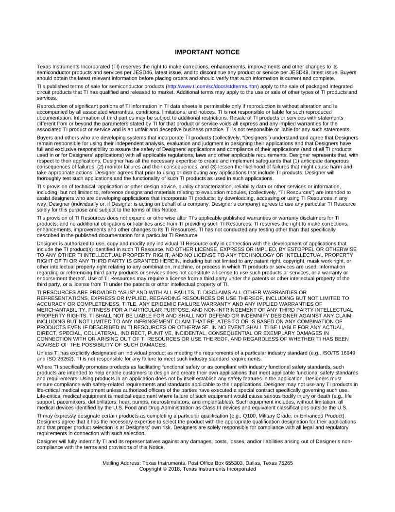
9.2 Typical ApplicationThis application example describes how to use the TLA2024 to monitor two different supply voltage rails in asystem. Figure 25 shows a typical implementation for monitoring two supply voltage rails.
Figure 25. Monitoring Two Supply Voltage Rails Using the TLA2024
9.2.1 Design RequirementsTable 8 lists the design requirements for this application.
Table 8. Design RequirementsDESIGN PARAMETER VALUEDevice supply voltage 3.3 VVoltage rails to monitor 1.8 V, 3.3 VMeasurement accuracy ±0.5%
Update rate 1 ms per rail
9.2.2 Detailed Design ProcedureThe analog inputs, AIN0 and AIN3, connect directly to the supply voltage rails that are monitored through RCfilter resistors. Small filter resistor values of 100 Ω are chosen to reduce voltage drops, and therefore offseterrors, caused by the input currents of the TLA2024 to a minimum. Filter capacitors of 0.47 µF are chosen to setthe filter cutoff frequencies at 3.39 kHz. In order to get one reading from each of the two supplies within 2 ms, adata rate of 2400 SPS is selected. The device is set up for single-ended measurements using MUX[2:0] settings100 and 101. A FSR = ±4.096 V is selected to measure the 3.3-V rail. The same FSR can also be used tomeasure the 1.8-V rail or the FSR can be set to FSR = ±2.048 V.

1
2
3
4
VDD
ADDR
GND
AIN0
AIN1
SCL
SDA
VDD
AIN3
AIN2
Device
NC
9
7
6
10
5
8
0.1 F
Temperature (qC)
Mea
sure
men
t Err
or (
%)
-40 -20 0 20 40 60 80 100-0.1
-0.075
-0.05
-0.025
0
0.025
0.05
0.075
0.1
3.3 V rail monitor1.8 V rail monitor
24
TLA2021, TLA2022, TLA2024SBAS846 –NOVEMBER 2017 www.ti.com
Product Folder Links: TLA2021 TLA2022 TLA2024
Submit Documentation Feedback Copyright © 2017, Texas Instruments Incorporated
9.2.3 Application CurveThe measurement results in Figure 26 show that the two supplies can be measured with ±0.5% accuracy overthe complete operating ambient temperature range without any offset or gain calibration.
Figure 26. Measurement Error vs Temperature
10 Power Supply RecommendationsThe device requires a single unipolar supply (VDD) to power the analog and digital circuitry of the device.
10.1 Power-Supply SequencingWait approximately 50 µs after VDD is stabilized before communicating with the device to allow the power-upreset process to complete.
10.2 Power-Supply DecouplingGood power-supply decoupling is important to achieve optimum performance. As shown in Figure 27, VDD mustbe decoupled with at least a 0.1-µF capacitor to GND. The 0.1-µF bypass capacitor supplies the momentarybursts of extra current required from the supply when the device is converting. Place the bypass capacitor asclose to the power-supply pin of the device as possible using low-impedance connections. Use multilayerceramic chip capacitors (MLCCs) that offer low equivalent series resistance (ESR) and inductance (ESL)characteristics for power-supply decoupling purposes. For very sensitive systems, or for systems in harsh noiseenvironments, avoid using vias to connect the capacitors to the device pins for better noise immunity. The use ofmultiple vias in parallel lowers the overall inductance and is beneficial for connections to ground planes.
Figure 27. TLA202x Power-Supply Decoupling

Device Microcontroller
Signal
Conditioning
(RC Filters
and
Amplifiers)
Supply
Generation
Connector
or Antenna
Ground Fill orGround Plane
Optional: S
plit
Gro
und
CutGround Fill or
Ground Plane
Optional: S
plit
Gro
und C
ut
InterfaceTransceiver
Ground Fill orGround Plane
Ground Fill orGround Plane
25
TLA2021, TLA2022, TLA2024www.ti.com SBAS846 –NOVEMBER 2017
Product Folder Links: TLA2021 TLA2022 TLA2024
Submit Documentation FeedbackCopyright © 2017, Texas Instruments Incorporated
11 Layout
11.1 Layout GuidelinesEmploy best design practices when laying out a printed-circuit board (PCB) for both analog and digitalcomponents. For optimal performance, separate the analog components such as ADCs, amplifiers, references,digital-to-analog converters (DACs), and analog MUXs from digital components such as microcontrollers,complex programmable logic devices (CPLDs), field-programmable gate arrays (FPGAs), radio frequency (RF)transceivers, universal serial bus (USB) transceivers, and switching regulators. Figure 28 shows an example ofgood component placement. Although Figure 28 provides a good example of component placement, the bestplacement for each application is unique to the geometries, components, and PCB fabrication capabilities. Thatis, there is no single layout that is perfect for every design and careful consideration must always be used whendesigning with any analog component.
Figure 28. System Component Placement
The following points outline some basic recommendations for the layout of the TLA202x to get the best possibleperformance of the ADC. A good design can be ruined with a bad circuit layout.
• Separate the analog and digital signals. To start, partition the board into analog and digital sections where thelayout permits. Route digital lines away from analog lines to prevent digital noise from coupling back intoanalog signals.
• Fill void areas on signal layers with ground fill.• Provide good ground return paths. Signal return currents flow on the path of least impedance. If the ground
plane is cut or has other traces that block the current from flowing right next to the signal trace, the groundplane must find another path to return to the source and complete the circuit. If the ground plane is forced intoa larger path, there is an increased chance of signal radiation. Sensitive signals are more susceptible to EMIinterference.
• Use bypass capacitors on supplies to minimize high-frequency noise. Do not place vias between bypasscapacitors and the active device. For best results, place the bypass capacitors on the same layer as close aspossible to the active device.
• Consider the resistance and inductance of the routing. Input traces often have resistances that react with theinput bias current and cause an added error voltage. Reduce the loop area enclosed by the source signal andthe return current to minimize the inductance in the path.
• For best input combinations with differential measurements, use adjacent analog input lines such as AIN0,AIN1 and AIN2, AIN3. The differential capacitors must be of high quality. The best ceramic chip capacitorsare C0G (NPO) capacitors, which have stable properties and low-noise characteristics.

SC
L
SD
A
AIN0AIN1
SCLSDA
VDD
AIN3
AIN2
1
GND
Device
AIN2
VDD
10
9
4
5
6
7
8
Vias connect to either bottom layer or an internal plane. The bottom layer or internal plane are dedicated GND planes
AD
DR
3
1
2 NC
ADDRAIN3
AIN
0
AIN
1
26
TLA2021, TLA2022, TLA2024SBAS846 –NOVEMBER 2017 www.ti.com
Product Folder Links: TLA2021 TLA2022 TLA2024
Submit Documentation Feedback Copyright © 2017, Texas Instruments Incorporated
11.2 Layout Example
Figure 29. TLA2024 X2QFN Package
27
TLA2021, TLA2022, TLA2024www.ti.com SBAS846 –NOVEMBER 2017
Product Folder Links: TLA2021 TLA2022 TLA2024
Submit Documentation FeedbackCopyright © 2017, Texas Instruments Incorporated
12 Device and Documentation Support
12.1 Device Support
12.1.1 Third-Party Products DisclaimerTI'S PUBLICATION OF INFORMATION REGARDING THIRD-PARTY PRODUCTS OR SERVICES DOES NOTCONSTITUTE AN ENDORSEMENT REGARDING THE SUITABILITY OF SUCH PRODUCTS OR SERVICESOR A WARRANTY, REPRESENTATION OR ENDORSEMENT OF SUCH PRODUCTS OR SERVICES, EITHERALONE OR IN COMBINATION WITH ANY TI PRODUCT OR SERVICE.
12.2 Related LinksThe table below lists quick access links. Categories include technical documents, support and communityresources, tools and software, and quick access to order now.
Table 9. Related Links
PARTS PRODUCT FOLDER ORDER NOW TECHNICALDOCUMENTS
TOOLS &SOFTWARE
SUPPORT &COMMUNITY
TLA2021 Click here Click here Click here Click here Click hereTLA2022 Click here Click here Click here Click here Click hereTLA2024 Click here Click here Click here Click here Click here
12.3 Receiving Notification of Documentation UpdatesTo receive notification of documentation updates, navigate to the device product folder on ti.com. In the upperright corner, click on Alert me to register and receive a weekly digest of any product information that haschanged. For change details, review the revision history included in any revised document.
12.4 Community ResourcesThe following links connect to TI community resources. Linked contents are provided "AS IS" by the respectivecontributors. They do not constitute TI specifications and do not necessarily reflect TI's views; see TI's Terms ofUse.
TI E2E™ Online Community TI's Engineer-to-Engineer (E2E) Community. Created to foster collaborationamong engineers. At e2e.ti.com, you can ask questions, share knowledge, explore ideas and helpsolve problems with fellow engineers.
Design Support TI's Design Support Quickly find helpful E2E forums along with design support tools andcontact information for technical support.
12.5 TrademarksE2E is a trademark of Texas Instruments.I2C, NXP Semiconductors are trademarks of NXP Semiconductors.All other trademarks are the property of their respective owners.
12.6 Electrostatic Discharge CautionThis integrated circuit can be damaged by ESD. Texas Instruments recommends that all integrated circuits be handled withappropriate precautions. Failure to observe proper handling and installation procedures can cause damage.
ESD damage can range from subtle performance degradation to complete device failure. Precision integrated circuits may be moresusceptible to damage because very small parametric changes could cause the device not to meet its published specifications.
12.7 GlossarySLYZ022 — TI Glossary.
This glossary lists and explains terms, acronyms, and definitions.

28
TLA2021, TLA2022, TLA2024SBAS846 –NOVEMBER 2017 www.ti.com
Product Folder Links: TLA2021 TLA2022 TLA2024
Submit Documentation Feedback Copyright © 2017, Texas Instruments Incorporated
13 Mechanical, Packaging, and Orderable InformationThe following pages include mechanical, packaging, and orderable information. This information is the mostcurrent data available for the designated devices. This data is subject to change without notice and revision ofthis document. For browser-based versions of this data sheet, refer to the left-hand navigation.

PACKAGE OPTION ADDENDUM
www.ti.com 28-Dec-2017
Addendum-Page 1
PACKAGING INFORMATION
Orderable Device Status(1)
Package Type PackageDrawing
Pins PackageQty
Eco Plan(2)
Lead/Ball Finish(6)
MSL Peak Temp(3)
Op Temp (°C) Device Marking(4/5)
Samples
TLA2021IRUGR ACTIVE X2QFN RUG 10 3000 Green (RoHS& no Sb/Br)
CU NIPDAU Level-1-260C-UNLIM -40 to 85 9AZ
TLA2021IRUGT ACTIVE X2QFN RUG 10 250 Green (RoHS& no Sb/Br)
CU NIPDAU Level-1-260C-UNLIM -40 to 85 9AZ
TLA2022IRUGR ACTIVE X2QFN RUG 10 3000 Green (RoHS& no Sb/Br)
CU NIPDAU Level-1-260C-UNLIM -40 to 85 19J
TLA2022IRUGT ACTIVE X2QFN RUG 10 250 Green (RoHS& no Sb/Br)
CU NIPDAU Level-1-260C-UNLIM -40 to 85 19J
TLA2024IRUGR ACTIVE X2QFN RUG 10 3000 Green (RoHS& no Sb/Br)
CU NIPDAU Level-1-260C-UNLIM -40 to 85 9IJ
TLA2024IRUGT ACTIVE X2QFN RUG 10 250 Green (RoHS& no Sb/Br)
CU NIPDAU Level-1-260C-UNLIM -40 to 85 9IJ
(1) The marketing status values are defined as follows:ACTIVE: Product device recommended for new designs.LIFEBUY: TI has announced that the device will be discontinued, and a lifetime-buy period is in effect.NRND: Not recommended for new designs. Device is in production to support existing customers, but TI does not recommend using this part in a new design.PREVIEW: Device has been announced but is not in production. Samples may or may not be available.OBSOLETE: TI has discontinued the production of the device.
(2) RoHS: TI defines "RoHS" to mean semiconductor products that are compliant with the current EU RoHS requirements for all 10 RoHS substances, including the requirement that RoHS substancedo not exceed 0.1% by weight in homogeneous materials. Where designed to be soldered at high temperatures, "RoHS" products are suitable for use in specified lead-free processes. TI mayreference these types of products as "Pb-Free".RoHS Exempt: TI defines "RoHS Exempt" to mean products that contain lead but are compliant with EU RoHS pursuant to a specific EU RoHS exemption.Green: TI defines "Green" to mean the content of Chlorine (Cl) and Bromine (Br) based flame retardants meet JS709B low halogen requirements of <=1000ppm threshold. Antimony trioxide basedflame retardants must also meet the <=1000ppm threshold requirement.
(3) MSL, Peak Temp. - The Moisture Sensitivity Level rating according to the JEDEC industry standard classifications, and peak solder temperature.
(4) There may be additional marking, which relates to the logo, the lot trace code information, or the environmental category on the device.
(5) Multiple Device Markings will be inside parentheses. Only one Device Marking contained in parentheses and separated by a "~" will appear on a device. If a line is indented then it is a continuationof the previous line and the two combined represent the entire Device Marking for that device.

PACKAGE OPTION ADDENDUM
www.ti.com 28-Dec-2017
Addendum-Page 2
(6) Lead/Ball Finish - Orderable Devices may have multiple material finish options. Finish options are separated by a vertical ruled line. Lead/Ball Finish values may wrap to two lines if the finishvalue exceeds the maximum column width.
Important Information and Disclaimer:The information provided on this page represents TI's knowledge and belief as of the date that it is provided. TI bases its knowledge and belief on informationprovided by third parties, and makes no representation or warranty as to the accuracy of such information. Efforts are underway to better integrate information from third parties. TI has taken andcontinues to take reasonable steps to provide representative and accurate information but may not have conducted destructive testing or chemical analysis on incoming materials and chemicals.TI and TI suppliers consider certain information to be proprietary, and thus CAS numbers and other limited information may not be available for release.
In no event shall TI's liability arising out of such information exceed the total purchase price of the TI part(s) at issue in this document sold by TI to Customer on an annual basis.

TAPE AND REEL INFORMATION
*All dimensions are nominal
Device PackageType
PackageDrawing
Pins SPQ ReelDiameter
(mm)
ReelWidth
W1 (mm)
A0(mm)
B0(mm)
K0(mm)
P1(mm)
W(mm)
Pin1Quadrant
TLA2021IRUGR X2QFN RUG 10 3000 180.0 8.4 1.75 2.25 0.65 4.0 8.0 Q1
TLA2021IRUGT X2QFN RUG 10 250 180.0 8.4 1.75 2.25 0.65 4.0 8.0 Q1
TLA2022IRUGR X2QFN RUG 10 3000 180.0 8.4 1.75 2.25 0.65 4.0 8.0 Q1
TLA2022IRUGT X2QFN RUG 10 250 180.0 8.4 1.75 2.25 0.65 4.0 8.0 Q1
TLA2024IRUGR X2QFN RUG 10 3000 180.0 8.4 1.75 2.25 0.65 4.0 8.0 Q1
TLA2024IRUGT X2QFN RUG 10 250 180.0 8.4 1.75 2.25 0.65 4.0 8.0 Q1
PACKAGE MATERIALS INFORMATION
www.ti.com 8-May-2018
Pack Materials-Page 1

*All dimensions are nominal
Device Package Type Package Drawing Pins SPQ Length (mm) Width (mm) Height (mm)
TLA2021IRUGR X2QFN RUG 10 3000 203.0 203.0 35.0
TLA2021IRUGT X2QFN RUG 10 250 203.0 203.0 35.0
TLA2022IRUGR X2QFN RUG 10 3000 203.0 203.0 35.0
TLA2022IRUGT X2QFN RUG 10 250 203.0 203.0 35.0
TLA2024IRUGR X2QFN RUG 10 3000 203.0 203.0 35.0
TLA2024IRUGT X2QFN RUG 10 250 203.0 203.0 35.0
PACKAGE MATERIALS INFORMATION
www.ti.com 8-May-2018
Pack Materials-Page 2


IMPORTANT NOTICE
Texas Instruments Incorporated (TI) reserves the right to make corrections, enhancements, improvements and other changes to itssemiconductor products and services per JESD46, latest issue, and to discontinue any product or service per JESD48, latest issue. Buyersshould obtain the latest relevant information before placing orders and should verify that such information is current and complete.TI’s published terms of sale for semiconductor products (http://www.ti.com/sc/docs/stdterms.htm) apply to the sale of packaged integratedcircuit products that TI has qualified and released to market. Additional terms may apply to the use or sale of other types of TI products andservices.Reproduction of significant portions of TI information in TI data sheets is permissible only if reproduction is without alteration and isaccompanied by all associated warranties, conditions, limitations, and notices. TI is not responsible or liable for such reproduceddocumentation. Information of third parties may be subject to additional restrictions. Resale of TI products or services with statementsdifferent from or beyond the parameters stated by TI for that product or service voids all express and any implied warranties for theassociated TI product or service and is an unfair and deceptive business practice. TI is not responsible or liable for any such statements.Buyers and others who are developing systems that incorporate TI products (collectively, “Designers”) understand and agree that Designersremain responsible for using their independent analysis, evaluation and judgment in designing their applications and that Designers havefull and exclusive responsibility to assure the safety of Designers' applications and compliance of their applications (and of all TI productsused in or for Designers’ applications) with all applicable regulations, laws and other applicable requirements. Designer represents that, withrespect to their applications, Designer has all the necessary expertise to create and implement safeguards that (1) anticipate dangerousconsequences of failures, (2) monitor failures and their consequences, and (3) lessen the likelihood of failures that might cause harm andtake appropriate actions. Designer agrees that prior to using or distributing any applications that include TI products, Designer willthoroughly test such applications and the functionality of such TI products as used in such applications.TI’s provision of technical, application or other design advice, quality characterization, reliability data or other services or information,including, but not limited to, reference designs and materials relating to evaluation modules, (collectively, “TI Resources”) are intended toassist designers who are developing applications that incorporate TI products; by downloading, accessing or using TI Resources in anyway, Designer (individually or, if Designer is acting on behalf of a company, Designer’s company) agrees to use any particular TI Resourcesolely for this purpose and subject to the terms of this Notice.TI’s provision of TI Resources does not expand or otherwise alter TI’s applicable published warranties or warranty disclaimers for TIproducts, and no additional obligations or liabilities arise from TI providing such TI Resources. TI reserves the right to make corrections,enhancements, improvements and other changes to its TI Resources. TI has not conducted any testing other than that specificallydescribed in the published documentation for a particular TI Resource.Designer is authorized to use, copy and modify any individual TI Resource only in connection with the development of applications thatinclude the TI product(s) identified in such TI Resource. NO OTHER LICENSE, EXPRESS OR IMPLIED, BY ESTOPPEL OR OTHERWISETO ANY OTHER TI INTELLECTUAL PROPERTY RIGHT, AND NO LICENSE TO ANY TECHNOLOGY OR INTELLECTUAL PROPERTYRIGHT OF TI OR ANY THIRD PARTY IS GRANTED HEREIN, including but not limited to any patent right, copyright, mask work right, orother intellectual property right relating to any combination, machine, or process in which TI products or services are used. Informationregarding or referencing third-party products or services does not constitute a license to use such products or services, or a warranty orendorsement thereof. Use of TI Resources may require a license from a third party under the patents or other intellectual property of thethird party, or a license from TI under the patents or other intellectual property of TI.TI RESOURCES ARE PROVIDED “AS IS” AND WITH ALL FAULTS. TI DISCLAIMS ALL OTHER WARRANTIES ORREPRESENTATIONS, EXPRESS OR IMPLIED, REGARDING RESOURCES OR USE THEREOF, INCLUDING BUT NOT LIMITED TOACCURACY OR COMPLETENESS, TITLE, ANY EPIDEMIC FAILURE WARRANTY AND ANY IMPLIED WARRANTIES OFMERCHANTABILITY, FITNESS FOR A PARTICULAR PURPOSE, AND NON-INFRINGEMENT OF ANY THIRD PARTY INTELLECTUALPROPERTY RIGHTS. TI SHALL NOT BE LIABLE FOR AND SHALL NOT DEFEND OR INDEMNIFY DESIGNER AGAINST ANY CLAIM,INCLUDING BUT NOT LIMITED TO ANY INFRINGEMENT CLAIM THAT RELATES TO OR IS BASED ON ANY COMBINATION OFPRODUCTS EVEN IF DESCRIBED IN TI RESOURCES OR OTHERWISE. IN NO EVENT SHALL TI BE LIABLE FOR ANY ACTUAL,DIRECT, SPECIAL, COLLATERAL, INDIRECT, PUNITIVE, INCIDENTAL, CONSEQUENTIAL OR EXEMPLARY DAMAGES INCONNECTION WITH OR ARISING OUT OF TI RESOURCES OR USE THEREOF, AND REGARDLESS OF WHETHER TI HAS BEENADVISED OF THE POSSIBILITY OF SUCH DAMAGES.Unless TI has explicitly designated an individual product as meeting the requirements of a particular industry standard (e.g., ISO/TS 16949and ISO 26262), TI is not responsible for any failure to meet such industry standard requirements.Where TI specifically promotes products as facilitating functional safety or as compliant with industry functional safety standards, suchproducts are intended to help enable customers to design and create their own applications that meet applicable functional safety standardsand requirements. Using products in an application does not by itself establish any safety features in the application. Designers mustensure compliance with safety-related requirements and standards applicable to their applications. Designer may not use any TI products inlife-critical medical equipment unless authorized officers of the parties have executed a special contract specifically governing such use.Life-critical medical equipment is medical equipment where failure of such equipment would cause serious bodily injury or death (e.g., lifesupport, pacemakers, defibrillators, heart pumps, neurostimulators, and implantables). Such equipment includes, without limitation, allmedical devices identified by the U.S. Food and Drug Administration as Class III devices and equivalent classifications outside the U.S.TI may expressly designate certain products as completing a particular qualification (e.g., Q100, Military Grade, or Enhanced Product).Designers agree that it has the necessary expertise to select the product with the appropriate qualification designation for their applicationsand that proper product selection is at Designers’ own risk. Designers are solely responsible for compliance with all legal and regulatoryrequirements in connection with such selection.Designer will fully indemnify TI and its representatives against any damages, costs, losses, and/or liabilities arising out of Designer’s non-compliance with the terms and provisions of this Notice.
Mailing Address: Texas Instruments, Post Office Box 655303, Dallas, Texas 75265Copyright © 2018, Texas Instruments Incorporated